theoretical background - shodhganga
TRANSCRIPT
Chapter 4
Theoretical background
4.1 Peripheral Component Interconnect Bus. 784.2 AVR 8 – bit Microcontroller family. 1164.3 PCI Interfacing chip. 1254.4 Microcontroller Programming Protocols – SPI and JTAG. 129
78
Chapter 4 Theoretical Background
The theoretical aspect of the devices and technologies used in the research
work is to be discussed before proceeding towards designing of the PCI bus
card. This chapter gives detail description of the following major topics that
are to be concentrated on.
Peripheral Component Interconnect Bus.
AVR 8 – bit Microcontroller family.
PCI Interfacing chip.
Microcontroller Programming Protocols – SPI and JTAG.
4.1 Peripheral Component Interconnect Bus.
4.1.1 About the PCI-SIG group and evolution of PCI bus
Formed in 1992, the PCI-SIG is the industry organization chartered to develop
and manage the PCI standard. With over 900 members, the PCI-SIG
effectively places ownership and management of the PCI specifications in the
hands of the developer community. A Board of Directors comprised of nine
people, each elected by the membership, leads the PCI-SIG.
The PCI-SIG is chartered to:
Maintain the forward compatibility of all PCI revisions or addenda
Contribute to both the establishment of PCI as an industry-wide
standard and to the technical longevity of the PCI architecture
Maintain the PCI specification as a simple, easy-to-implement, stable
technology that supports the spirit of its design
The PCI-SIG fulfills its charter by continuing to promote innovation and evolve
the PCI standard to meet the industry's needs. Through interoperability
testing, technical support, seminars and industry events, the PCI-SIG enables
its members to generate competitive and quality products.
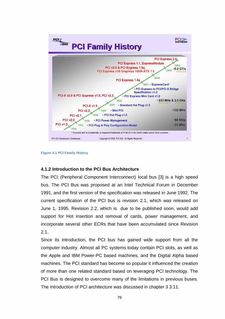
The figure 4.1 shows the evolution of PCI Bus family history.
79
Figure 4.1 PCI Family History
4.1.2 Introduction to the PCI Bus Architecture
The PCI (Peripheral Component Interconnect) local bus [3] is a high speed
bus. The PCI Bus was proposed at an Intel Technical Forum in December
1991, and the first version of the specification was released in June 1992. The
current specification of the PCI bus is revision 2.1, which was released on
June 1, 1995. Revision 2.2, which is due to be published soon, would add
support for Hot insertion and removal of cards, power management, and
incorporate several other ECRs that have been accumulated since Revision
2.1.
Since its introduction, the PCI bus has gained wide support from all the
computer industry. Almost all PC systems today contain PCI slots, as well as
the Apple and IBM Power-PC based machines, and the Digital Alpha based
machines. The PCI standard has become so popular it influenced the creation
of more than one related standard based on leveraging PCI technology. The
PCI Bus is designed to overcome many of the limitations in previous buses.
The introduction of PCI architecture was discussed in chapter 3 3.11.
80
The major benefits of using PCI are:
High speed
The PCI bus can transfer data at a peak rate of 132MBytes/sec using the
current 32 bit data path and a 33MHz clock speed. Future implementations
featuring a 64 bit data path and 66MHz clock speed may transfer data as fast
as 524MBytes/sec. Even at its basic mode, PCI delivers more than tenfold the
performance levels offered by its predecessor in the PC world, the ISA bus.
Expandability
The PCI bus can be expanded to a large number of slots using PCI to PCI
bridges. The bridge units connect separate small PCI buses to form a single,
unified, hierarchical bus. When traffic is local to each bus, more than one bus
may be active concurrently. This allows load balancing, while still allowing any
PCI Master on any bus to access any PCI Target on any other PCI bus.
Low Power
Motherboards can lower their power requirement by reducing the clock rate as
low as 0Hz (DC). All PCI compliant cards are required to operate in all
frequency ranges from 0Hz to 33MHz.
Automatic Configuration
All PCI compliant cards are automatically configured. There is no need to set
up jumpers to set the card's I/O address, IRQ number, or DMA channel
number. The PCI BIOS software is responsible for probing all the PCI cards in
a system, and assigning resources to every card, as required.
Future expansion
The PCI specification can support future systems by incorporating features
such as an optional 64 bit address space, and 66MHz bus speed. The
specification defines enough reserved fields in all the bus definitions
(configuration space registers, bus commands, and addressing modes), that
any unforeseen enhancement will not hinder compatibility with present
systems.
Portability

81
By incorporating the (optional) OpenBoot standard, any device with OpenBoot
Firmware can boot systems containing any microprocessor and O/S. Even
without OpenBoot, it is common to see drivers for many video cards and SCSI
controller for multiple CPU architectures and operating systems.
Complex memory hierarchy support
The PCI Bus supports advanced features such as bus snooping to allow
cache coherency to be kept even with multiple bus masters, and a locking
mechanism to support semaphores.
Interoperability with existing standards
The PCI Bus allows interoperability with existing ISA cards by supporting
subtractive decoding of addresses (allowing addresses not decoded by PCI
cards to be routed to an ISA backplane). The standard also supports the fixed
legacy addresses for VGA cards and IDE controllers (required for system
boot). Another feature supporting backward compatibility allows different
devices to respond to different I/O byte addresses even if they share the
same 32 bit word.
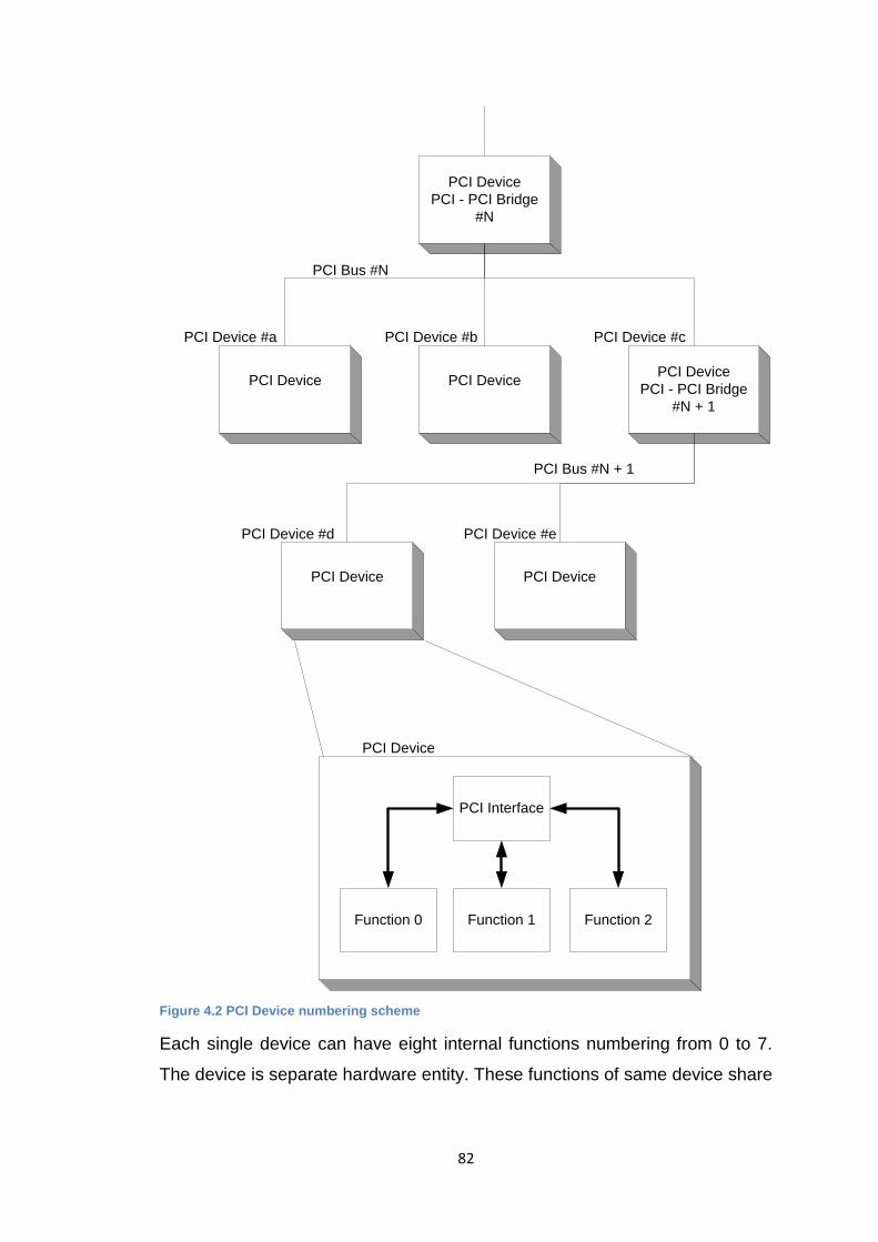
The PCI device can be identified by its functions and device numbering as
shown in figure 4.2
82
PCI Device
PCI - PCI Bridge
#N
PCI DevicePCI Device
PCI Device
PCI - PCI Bridge
#N + 1
PCI DevicePCI Device
PCI Interface
Function 2Function 1Function 0
PCI Device
PCI Bus #N
PCI Bus #N + 1
PCI Device #a
PCI Device #ePCI Device #d
PCI Device #cPCI Device #b
Figure 4.2 PCI Device numbering scheme
Each single device can have eight internal functions numbering from 0 to 7.
The device is separate hardware entity. These functions of same device share
83
the same PCI bus. A specific function is selected by ‗Bus number/Device
number/Function number‘
The PCI (Peripheral Component Interconnect) local bus is a high-performance
connection between motherboard components and expansion boards. It was
first proposed at an Intel Technical Forum in December 1991, and the first
version of the specification was released in June 1992. The PCI Steering
Committee members who developed the initial version of the specification
were Compaq, DEC, IBM, Intel, and NCR. In June 1992, PCI became an
open industry standard controlled by the newly formed PCI SIG (PCI Special
Interest Group). In April 1993, revision 2.0 of the PCI specification was
released.
Vendor support for the PCI standard has been widespread. Apple has
announced that it will support the PCI bus in a future version of its PowerPC
RISC Macintosh. (Note that first-generation PowerPC Macs will use the
NuBus to support existing NuBus peripheral boards.) DEC intends to support
PCI in its Alpha-based systems, and the company's high-speed DECchip
210066 RISC processor implements a PCI interface on the chip itself. This
kind of support, in addition to that from many vendors of 80x86-based
systems, paves the way for PCI to become a universally accepted component
interconnect and expansion-bus standard.
The motivation for PCI was the fact that PC I/O architecture was so slow in
relation to the processor that further improvements in processor technology
would not have produced any noticeable improvements in overall system
performance. PCI removes systems designers from the processor treadmill by
isolating the I/O subsystem from the processor/memory/cache subsystem.
A fundamental part of a PCI design is the PCI-to-host bridge chip that
connects the PCI bus to the processor's local bus. PCI peripherals are then
connected directly to the PCI bus. Once a host bridge chip is available, a new
processor has access to all available PCI components. This allows the PCI
bus standard to be processor independent.
When a new processor becomes available, only the PCI-to-host bridge chip
needs to be replaced; the rest of the system remains unchanged. PCI is a
component- and board-level bus; other I/O buses, such as a SCSI bus, can
be included in a PCI system with a controller chip or a board that interfaces to
84
the PCI bus. Designers of I/O components such as graphics, SCSI, or LAN
controllers can now concentrate on improving the performance of their
products instead of continually redesigning their products for different
processor speeds and bus types.
Although processors are quickly moving past 33-MHz operation, the PCI bus
is defined to operate only up to 33 MHz. The processor speed can be faster
than the PCI bus speed, however, because the host-to-PCI bridge isolates the
processor bus from the PCI bus. The bridge chip can contain buffering to
enhance performance and bus utilization. This is especially useful when using
a processor, such as the 486, that doesn't support burst writes. Since the PCI
bus does support burst writes, the host bridge can buffer a nonburst write
from the processor and present it to the PCI bus as a burst write. A bridge
might contain other system-support logic, such as for a cache controller or for
handling the PCI bus's centralized arbitration mechanism.
PCI won't replace the standard expansion buses that are popular today, but
instead it will complement them. These expansion buses are added to a PCI
system by the inclusion of a PCI-to-expansion bus bridge chip. The standard
expansion buses (e.g., ISA, EISA, Micro Channel, and NuBus) are lower in
performance, but they provide for maximum system expandability for less-
demanding peripherals.
4.1.3 PCI Bus Design
The design goals of the PCI bus standard were threefold. First, it would
produce a low-cost, high-performance local-bus interface. Second, it would
provide automatic configuration of components and add-in boards. Finally, the
design would have the versatility to support future generations of peripherals.
The cost and size of connectors, chips, and motherboard traces increase as
the number of pins needed to implement a bus increases. The PCI standard
reduces costs by using a multiplexed address and data bus that reduces the
pin count and size of the components. A PCI target (which is defined later)
can be implemented with only 47 pins, and a PCI master can be implemented
with only 49 pins.
Despite the small number of lines, this setup can manage bus addressing,
data transfer, arbitration logic, and interface control. The figure "PCI Interface
Signals" lists the PCI bus pins, with both the required and optional pins

85
shown. Note that the optional pins provide support for a cache and atomic
operations. Other optional pins implement a 64-bit bus, giving the PCI
standard a growth path for future systems.
Two sizes of add-in boards are specified: a standard length (about 12 inches
long) and a short length (about 7 inches long). Note that the PCI bus is limited
to 10 loads. Chips on the motherboard take up one load each, and add-in
boards in PCI slots consume two loads each. For example, if devices on the
motherboard consume four loads, this leaves six loads available, allowing
three PCI slots. Too much loading can cause signals to violate timing
specifications, which leads to system failures.
PCI Universal Card 32/64 bit
----------------------------------------------------------------
| PCI Component Side (side B) |
| |
| |
| optional |
| ____ mandatory 32-bit pins 64-bit pins _____|
|___| |||||||--|||||||||||||||||--|||||||--||||||||||||||
^ ^ ^ ^ ^ ^ ^ ^
b01 b11 b14 b49 b52 b62 b63 b94
PCI 5V Card 32/64 bit
| optional |
| ____ mandatory 32-bit pins 64-bit pins _____|
|___| ||||||||||||||||||||||||||--|||||||--||||||||||||||
PCI 3.3V Card 32/64 bit
| optional |
| ____ mandatory 32-bit pins 64-bit pins _____|
|___| |||||||--||||||||||||||||||||||||||--||||||||||||||
Figure 4.3 Universal PCI Slot
The PCI specification defines two types of connectors that may be
implemented at the system board level: One for systems that implement 5
Volt signaling levels, and one for systems that implement 3.3 Volt signaling
86
levels. In addition, PCI systems may implement either the 32-bit or 64-bit
connector. Most PCI buses implement only the 32-bit portion of the connector
which consists of pins 1 through 62. Advanced systems which support 64-bit
data transfers implement the full PCI bus connector which consists of pins 1
through 94. Three types of add-in boards may be implemented: "5 Volt add-in
boards" include a key notch in pin positions 50 and 51 to allow them to be
plugged only into 5 Volt system connectors. "3.3 Volt add-in boards" include a
key notch in pin positions 12 and 13 to allow them to be plugged only into 3.3
Volt system connectors. "Universal add-in boards" include both key notches to
allow them to be plugged into either 5 Volt or 3.3 Volt system connectors.
To accommodate the industry's shift from 5-V signals to 3.3-V signals, PCI
also defines a 3.3-V PCI specification. PCI add-in boards and slots are keyed
so that 5-V boards plug only into corresponding 5-V PCI slots and 3-V boards
plug only into 3-V slots. The PCI SIG is encouraging add-in board vendors to
design "universal" boards that operate at both voltages and can plug into
either a 5- or a 3.3-V PCI slot (see the figure 4.3).
PCI defines three types of address space: memory, I/O, and configuration.
Configuration space is a 256-byte area inside each PCI device that contains
information about the device. Such information includes the type code, which
indicates whether the device controls a mass-storage unit, a network
interface, a display, or other hardware. Multifunction devices are supported,
as long as there is only one physical connection to the PCI bus, such as one
chip that supports both SCSI and Ethernet. The configuration space also
contains the PCI control, status, and latency timer registers; the location of the
device's expansion ROM; and the base-address registers. At power-up, the
system scans the configuration space of all devices on the PCI bus and then
assigns each device a unique base address and an interrupt level.
A PCI device's expansion ROM contains code to initialize the device, or
devices. The ROM's contents are arranged in little-endian (i.e., Intel) format,
but there's nothing in the design to prohibit other processors from making use
of the information. The ROM can contain different code images that initialize
the device for different processor architectures. PCI provides true plug-and-
play; the system takes care of hardware configuration automatically. A user
just plugs in a board, and it works.
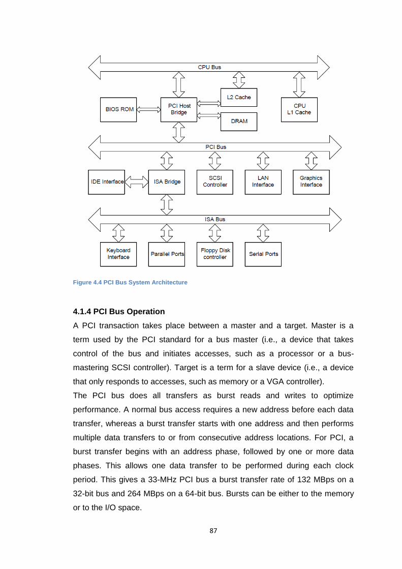
87
Figure 4.4 PCI Bus System Architecture
4.1.4 PCI Bus Operation
A PCI transaction takes place between a master and a target. Master is a
term used by the PCI standard for a bus master (i.e., a device that takes
control of the bus and initiates accesses, such as a processor or a bus-
mastering SCSI controller). Target is a term for a slave device (i.e., a device
that only responds to accesses, such as memory or a VGA controller).
The PCI bus does all transfers as burst reads and writes to optimize
performance. A normal bus access requires a new address before each data
transfer, whereas a burst transfer starts with one address and then performs
multiple data transfers to or from consecutive address locations. For PCI, a
burst transfer begins with an address phase, followed by one or more data
phases. This allows one data transfer to be performed during each clock
period. This gives a 33-MHz PCI bus a burst transfer rate of 132 MBps on a
32-bit bus and 264 MBps on a 64-bit bus. Bursts can be either to the memory
or to the I/O space.
88
PCI burst transfers have an indefinite length, whereas most other
architectures have a limited, fixed burst length. PCI bursts continue until the
master or target requests the transfer to end or until a higher-priority device
needs to use the bus. Each PCI device has a latency timer that defines the
longest period of time that that device is allowed to use the PCI bus. This
timer is accessed through the configuration space and is programmed by the
processor. The processor can optimize overall system performance by
intelligently programming the latency timers of all devices on the PCI bus.
The master specifies the type of burst transaction by using bus commands.
Another way to improve the performance of any bus running at a particular
speed is to reduce its overhead, which is time that the bus is in use but data is
not being transferred. When a PCI device wants to access the PCI bus, it
must request use of the bus from the central arbiter (which can be located in
the PCI-to-host chip) by using its REQ (request) signal. The arbiter uses its
GNT (grant) signal to allow the device to use the bus. On most buses in use
today, the arbitration process takes up cycles that could be spent transferring
data. PCI eliminates this loss by allowing the arbitration for the next access to
occur while the current access is still in progress.
The PCI bus can transfer data 32 bits or 64 bits at a time. The optional signals
REQ64 and ACK64 allow a 64-bit master to ask if a target is capable of 64-bit
data transfers. A 64-bit transfer occurs only if a master asks for a 64-bit
transfer and a target responds that it can do such transfers.
A PCI master can support 32- or 64-bit addressing regardless of whether it
supports a 32- or a 64-bit data path. Since a master might not be able to look
at a target's configuration space, a master that supports 64-bit addressing
doesn't always know if a target supports 32- or 64-bit addressing. Therefore,
the master must be able to present an address in a format that either type of
target can accept. The master addresses 32- or 64-bit devices capable of 64-
bit addressing by issuing a dual-address-cycle command.
To implement such a command, during the first address cycle the master first
drives the lower 32 bits of the 64-bit address on the lower 32 bits of the bus,
and the upper 32 bits of the 64-bit address on the upper 32 bits of the bus.
During the second address cycle, the upper 32 bits of the 64-bit address are
driven again, but this time on the lower 32 bits of the bus.
89
A 64-bit target will take in the full 64 bits of the address on the first clock cycle,
ignore the second address phase, and decode the 64-bit address with no
additional delay. A 32-bit target must wait an additional clock cycle to receive
the full 64-bit address, since it is transferred in two 32-bit portions. Targets
that support only 32-bit addressing are mapped into the lower 32 bits (4 GB)
of address space, so they can be accessed by masters that support 32- or 64-
bit addressing transparently.
4.1.5 The PCI Bus Signal Description
The PCI Bus is a multiplexed, synchronous, 32 bit bus. A minimal PCI target
interface consists of 47 signals, while a master or master/target interface
requires a minimum of 49 signals. The following paragraphs summarize the
PCI signals. It is not intended to be a PCI design reference, only to illustrate
very generally how PCI works. In order to design a fully compliant PCI card,
please refer to the PCI standard [(PCISIG, 1995)].
4.1.5.1 Signal types
The PCI standard defines a few signal types:
t/s
Tri State. Signals of this type are shared bus signals and may be driven
by only one driver at a time. The rest of the bus peripherals should tri-
state signals of this type when not in use. When one driver stops driving
a t/s signal, a new driver must wait at least one cycle before it can drive the
same signal. This is called bus turnaround and is used to prevent any
case where two or more drivers are trying to drive the same line.
Example: AD[31:0], /C/BE[3:0], PAR, /REQ, /GNT, AD[63:32],
/C/BE[7:4], PAR64.
s/t/s
Sustained Tri-State. Signals of this type are tri state signals. The
difference between these signals and normal t/s signals is that any driver
driving these signals must drive them high for at least one cycle before tri-
stating them. By driving the signal high, the line is charged so when it is tri-
90
stated one cycle later, it will stay high. This allows rapid switching from one
driver to another, without undefined logic levels in between.
Example: /FRAME , /TRDY , /IRDY , /STOP ,/LOCK , /DEVSEL ,
/PERR , /REQ64 , /ACK64 .
o/d
Open Drain. Signals of this type are wired-ORed. Multiple drivers may
drive this signal to a low state. When no driver is driving the signal, a pull-up
resistor is used to keep it in the high state.
Example: SERR , /INTA , INTB , INTC , INTD .
in
Input. Signals of this type are always input.
Example: CLK, /RST , IDSEL, TCK, TDI, TMS, TRST .
out
Output. Signals of this type are always output.
Example: TDO.
4.1.5.2 System Signals
CLK
All the PCI Bus signals are fully synchronized to the PCI Clock signal, CLK.
RST
This is the PCI Bus reset signal. It is asynchronous to the PCI clock signal.
4.1.5.3 Address/Data and Command
AD[31:0] t/s
This is the multiplexed address/data bus. All PCI transactions begins by a
Master driving the address on the 1st cycle. When the Master is doing a read
transaction, the 2nd cycle is a turnaround cycle in which the Master tri-states
the bus and the target enables it‘s data buffers to drive the results on the bus.
The actual data is transferred only beginning on the 3rd cycle onwards. When
a Master is doing a write transaction, it can begin driving the write data on the
2nd cycle, because no turnaround cycle is needed (the bus does not change
direction).
C/BE [3:0] t/s
91
These are dual function pins, and are always driven by the Master. During the
1st cycle, when AD[31:0] is driving the address, C/BE [3:0] is driving the bus
command (Memory read, Memory
write, etc.). When AD[31:0] is driving the data, C/BE [3:0] drive the byte
enable for each byte lane on the data bus. During a write transaction, the
Master drives C/BE [3:0] with information specifying which byte lanes contain
valid data. During a read transaction, the Master drives C/BE [3:0] with
information specifying which byte lanes are requested by the master.
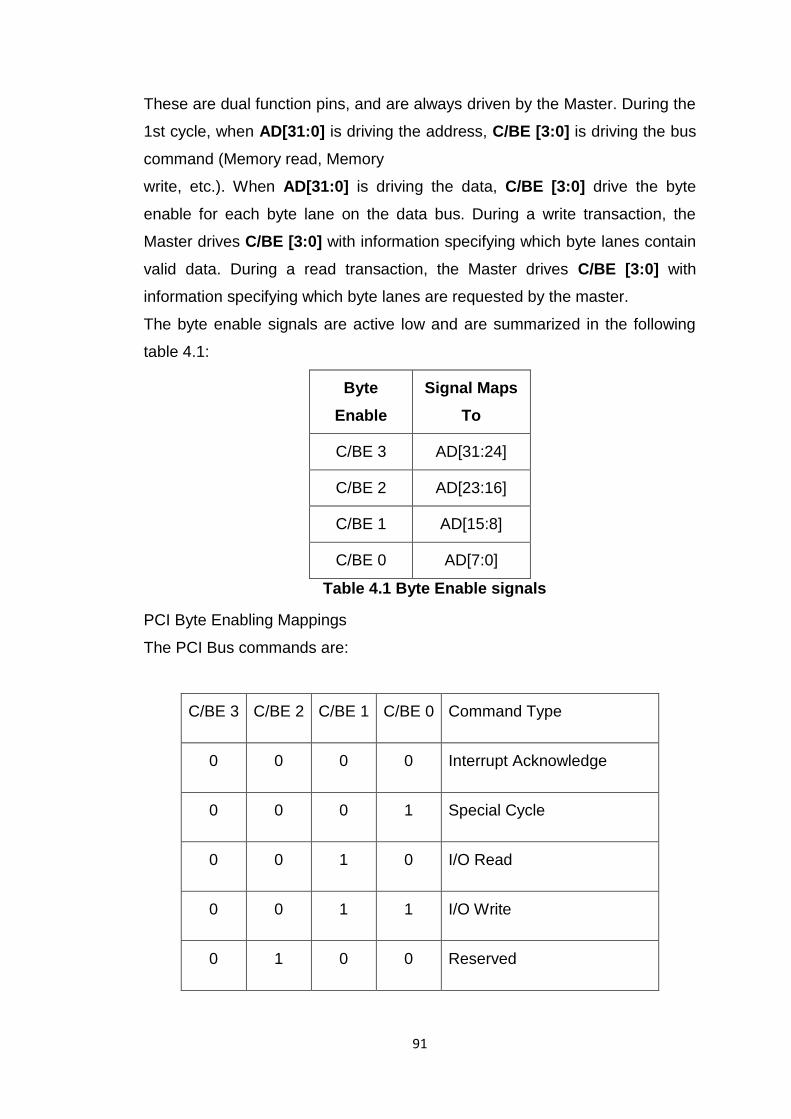
The byte enable signals are active low and are summarized in the following
table 4.1:
Byte
Enable
Signal Maps
To
C/BE 3 AD[31:24]
C/BE 2 AD[23:16]
C/BE 1 AD[15:8]
C/BE 0 AD[7:0]
Table 4.1 Byte Enable signals
PCI Byte Enabling Mappings
The PCI Bus commands are:
C/BE 3 C/BE 2 C/BE 1 C/BE 0 Command Type
0 0 0 0 Interrupt Acknowledge
0 0 0 1 Special Cycle
0 0 1 0 I/O Read
0 0 1 1 I/O Write
0 1 0 0 Reserved
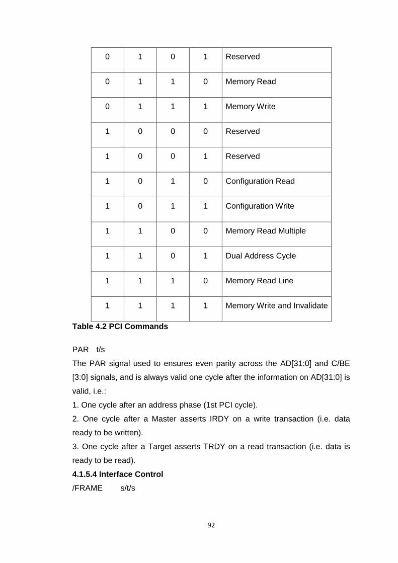
92
0 1 0 1 Reserved
0 1 1 0 Memory Read
0 1 1 1 Memory Write
1 0 0 0 Reserved
1 0 0 1 Reserved
1 0 1 0 Configuration Read
1 0 1 1 Configuration Write
1 1 0 0 Memory Read Multiple
1 1 0 1 Dual Address Cycle
1 1 1 0 Memory Read Line
1 1 1 1 Memory Write and Invalidate
Table 4.2 PCI Commands
PAR t/s
The PAR signal used to ensures even parity across the AD[31:0] and C/BE
[3:0] signals, and is always valid one cycle after the information on AD[31:0] is
valid, i.e.:
1. One cycle after an address phase (1st PCI cycle).
2. One cycle after a Master asserts IRDY on a write transaction (i.e. data
ready to be written).
3. One cycle after a Target asserts TRDY on a read transaction (i.e. data is
ready to be read).
4.1.5.4 Interface Control
/FRAME s/t/s

93
The /FRAME signal is used to start a PCI transaction. When the PCI bus is
Idle, /FRAME is high. When a Master begins a new PCI transaction, /FRAME
is driven low. /FRAME is kept low during all the transaction, until (but not
including) the last data item transferred. When a Master read or writes the last
data item in a burst access cycle, /FRAME will be driven high when IRDY is
driven low for the last time.
/IRDY s/t/s
/IRDY is used by the Master to indicate its readiness to perform data transfer
on a word by word basis. When a Master is reading data, it will drive /IRDY
high, until it can accept a data word. The Master will then drive /IRDY low on
the same cycle it samples the data from the Target. When a Master is writing
data, it will drive /IRDY high until AD[31:0] contains a valid data word to be
written. It will then drive /IRDY low on the same cycle AD[31:0] is valid for
write. The actual data transfer will take place only when both /IRDY and
TRDY are active. Once driven low, /IRDY cannot be driven high until the
current bus transaction is done (i.e. /TRDY or STOP also driven low).
TRDY s/t/s
/TRDY is used by the Target to indicate its readiness to perform data transfer
on a word by word basis. When a Target is accepting data (Master writing
data), it will drive /TRDY high until it can accept the data word. The Target will
then drive /TRDY low on the same cycle it samples the data item from
AD[31:0]. When a Target is supplying data (Master reading data), it will drive
/TRDY high until it can drive AD[31:0] with the requested data. The Target will
then drive /TRDY low on the same cycle it drives the requested data item on
AD[31:0]. The actual data transfer will take place only when both /IRDY and
/TRDY are active. Once driven low, /TRDY cannot be driven high until data is
transferred (i.e. IRDY also driven low).
DEVSEL s/t/s
/DEVSEL is used by the Target to acknowledge the Master it is handling the
current bus cycle. When a Master begins a read/write transaction, it drives
/FRAME low on the 1st cycle, together with the requested address on
AD[31:0]. All the Targets on the bus recognize the beginning of a new
transaction by /FRAME going low, and compare the address on AD[31:0] with
their base address registers. The Master expects one Target, who‘s address
94
range contains the address driven on AD[31:0] to respond with a low DEVSEL
within 4 clock cycles. If no target responds within 4 cycles, the Master
assumes that no Target exists on the bus at the specified address, and the
transaction is aborted by the Master.
IDSEL in
/IDSEL / is used by the Master to perform system configuration. A target will
accept a configuration transaction only when /IDSEL is driven high on the 1st
cycle. Since every PCI slot has a unique /IDSEL line, every slot can be
uniquely accessed even before it's configured1. Empty PCI slots can be
identified since no /DEVSEL would be driven as a response to a configuration
access for that slot.
STOP s/t/s
/STOP is used by the Target to end the current burst read or write transaction.
If a Master samples /STOP low during a data word transfer, it must disconnect
the bus and end the transaction. The state of /TRDY and /DEVSEL while
STOP was driven indicates the termination type: Disconnect with data,
Disconnect without data, Target retry , or Target abort.
4.1.5.5 Arbitration
REQ t/s2
/REQ is used only by bus Masters. When a Master wants to begin a
transaction, it must first acquire the bus by driving /REQ low. All the /REQ
lines from all the PCI slots supporting bus masters are connected to a central
PCI Bus Arbiter, which will grant the bus only to one PCI Master at a time.
GNT t/s
/GNT is used only by bus Masters. /GNT is driven low by the central PCI Bus
Arbiter to the PCI Bus Master when the Master is granted the use the shared
PCI bus. /GNT lines are unique to every PCI slot supporting bus Masters.
When a Bus Master receives /GNT low, it is allowed to access the PCI bus
1The PCI standard does not define a standard way in which a Master can drive a specific IDSEL line! On
most PC based platforms, each slot has its IDSEL line connected through a resistor to one of the AD lines,
usually beginning with AD16 for the 1st slot. A Master will select the specific slot configuration space by
making sure it drives an address enabling only a single card with IDSEL. Driving more than one card with
IDSEL will cause bus clashes when both cards drives DEVSEL , trying to accept the cycle, and may even
lead to hardware malfunctions. 2 Notice that both REQ and GNT are marked as t/s. This is because the signals must be tri stated when the
PCI bus is reset.
95
only after the current cycle taking place is ended. This is indicated by both
/FRAME and /IRDY being high.
4.1.5.6 Error Reporting
PERR s/t/s
/PERR is used by a PCI card to report parity errors on the data phase. /PERR
is driven by the Master during a data read, and by the Target during a data
write. /PERR timing is one cycle after PAR is driven with a valid value. (PAR
is driven by the Target during a data read, and by the Master during a data
write). Reporting parity error via /PERR is optional, and can be turned off by
clearing a control bit in the Target or Master configuration space. Also notice
that address phase parity errors should not be reported with /PERR.
SERR o/d
/SERR is used by the Target or the Master to signal a system error condition,
such as parity error during a transaction address phase (The 1st cycle, when
the address is transmitted). Unlike /PERR, /SERR can be driven by any PCI
target at any time since it is open drain. It is pulled high by a resistor located
on the motherboard, or on another central resource. /SERR should be used
with care, since on most system today it is meant to indicate a fatal system
error which might imply a system reset!
4.1.5.7 64 Bit Extension
The following signals exist only on 64 bit PCI cards or slots. The signals are
available on a secondary connector, similar to the ISA 16 bit extension of the
XT bus. Using 64 bit cards on 32 bit slots (in 32 bit mode of course) is
permitted, as well as using 32 bit cards in 64 bit slots.
AD[63:32] t/s
AD[63:32] are used to hold the extra 32 data bits during 64 bit data transfer,
and to hold the extra 32 address bits when accessing a resource located in
the 64 bit memory space.
C/BE [7:4] t/s
During the address phase of a 64 bit PCI transaction, C/BE [7:4] are unused.
During the data phase, the C/BE [7:4] lines are used just like the C/BE [3:0]
lines, indicating which byte lanes are valid.
PAR64 t/s
96
/PAR64 is used in the same was as PAR, but contains the parity only for the
AD[63:32] and C/BE [7:4] lines. It obeys the same timing rules as PAR.
REQ64 s/t/s
/REQ64 is used by a 64 bit master to request a 64 bit cycle. It obeys the same
timing rules as the /FRAME signal.
ACK64 s/t/s
/ACK64 is used by the target to accept a request for a 64 bit cycle. It obeys
the same timing rules as the /DEVSEL signal.
4.1.5.8 Bus Snooping
The bus snooping lines allows a PCI bus master containing a write back
cache to maintain the data coherency on systems with multiple bus masters.
For example, Bus master ―A‖ contains a modified copy of memory location ―X‖
on his write back cache. In the same time, other bus masters may
independently try to modify memory location ―Y‖, sharing the same cache line
as memory location ―X‖. Since the cache logic writes back to memory whole
cache lines, Bus master ―A‖ must write back it's modified copy of the cache
line before the other master can write location ―Y‖, because otherwise any
new value for ―Y‖ would be overwritten when Bus master ―A‖ would write back
its modified cache line containing ―X‖.
SDONE in/out3
SDONE is used by a bus master containing a write back cache to signal the
currently addresses target not to acknowledge the current cycle until the
master finishes searching for the specified address in its write back cache.
SDONE Will be high during the search, and low on the 1st cycle the search is
completed.
SBO in/out
/SBO is driven high during the snoop address search (see above). If the
address requested is cached in the local write back cache and is dirty, SBO
will go low on the same cycle SDONE goes high, to signal a back-off
command to the target, so the modified cache line can be flushed. If /SBO
goes high when SDONE goes high, the requested address is not in the
master‘s cache, and the cycle can continue normally.
3 SDONE and SBO are in for PCI targets and out for PCI masters.
97
4.1.5.9 JTAG (IEEE 1149.1)
JTAG is an IEEE standard defining a serial bus for system testing. JTAG is
used by many chip vendors for:
1. Board testing A PCB connectivity netlist can be verified by bypassing the
output and input logic on the chip's I/O pads and drive out test values. By
chaining all the chips on a PCB with JTAG, it is possible to test the PCB
connectivity after manufacturing or during maintenance by driving values
through an I/O pin using the JTAG port of the source chip, and reading those
values on another I/O pin using the JTAG port on the target chip.
2. Software debugging of Microprocessors Most new microprocessors
supports JTAG for the use of a background debug mode. This mode allows
reading and writing internal CPU registers, inserting breakpoints, single
stepping the CPU and even get a limited back trace. (For example, some
members of the Motorola 683XX family). This gives designers most of the
capabilities of an expensive ICE at fraction of the price.
3. In-System-Programming of programmable logic devices
Most of the large pin count FPGAs and CPLDs today use PQFP packages
which are soldered directly to the board during manufacturing. When using
multiple chips it is very expensive to program these chips on a programmer. It
is also impossible to reprogram the devices once they are soldered. Instead,
CPLDs and FPGA chips are soldered to the board while they are still blank,
and are chained together on the board by a JTAG chain. A single JTAG
connector on the board can then be used to program all the chips without
using an expensive and unreliable PQFP adapter for off-board chip
programming. Unfortunately, the PCI committee never defied a standard way
to access the JTAG port on the PCI motherboard, nor did it define the JTAG
bus topology. Because of this, only a few PCI designs supported the JTAG
pins on the PCI connector. Some motherboard manufacturers has even went
as far as violating the PCI spec and using the JTAG lines for an entirely
different purpose such as Video sideband signals!
TDI
TDI is a Test Input pin, and it is used to shift data and instructions into the
JTAG port.
TDO
98
TDO is used to shift data out from the JTAG port.
TCK
TCK is the JTAG clock. It is used to control the data shifting in and out of the
JTAG port.
TMS
TMS is used to select the JTAG mode.
TRST
TRST is used to reset the JTAG port.
4.1.6 The PCI Bus Commands
As we have seen in section 4.1.5.3, the PCI Bus has defined 12 different
commands and reserved 4 commands. The following paragraph contains a
very short description of all the PCI Bus commands. We will take a closer look
at the commands later, in section 4.1.9.
Memory Read
A Memory Read command is used by a PCI bus master to read one or more
memory locations from a PCI bus target. It is recommended that Masters use
this command when reading less than one cache line.
Memory Read Line
This command is the same as the Memory Read command, with the
exception that the bus master is intending to read at least a cache line. This is
a hint to the Target, which may use this hint to prefetch more data in advance,
or it may choose to ignore it and treat this command in the same way as the
Memory Read command. It is recommended that Masters use this command
when reading between 1 to 2 cache lines.
Memory Read Multiple
This command is the same as the Memory Read command, with the
exception that the bus master is guaranteed to read one or more cache lines.
This is a hint to the target, which may use this hint to prefetch more data in
advance, or it may choose to ignore it and treat this command in the same
way as the Memory Read command. It is recommended that Masters use this
command when reading 2 or more cache lines.
Memory Write
A Memory Write command is used by a PCI Bus master to write one or more
memory locations to a PCI target.
99
Memory Write and Invalidate
This command is the same as the Memory Write command, with the
exception that the Master is guaranteed to write one or more whole cache
lines. This command is used to disable the snooping mechanism, because
writing an entire cache line means that any dirty data located in any cache is
now invalid and shouldn‘t be written back. When using this command, the
master must never write incomplete cache lines.
I/O Read
An I/O Read command is used by a PCI bus master to read the one or more
I/O locations from a PCI target.
I/O Write
An I/O Write command is used by a PCI bus master to write one or more I/O
locations to a PCI target.
Configuration Read
A Configuration Read command is used by a PCI bus master to read one or
more Configuration registers from a PCI target.
Configuration Write
A Configuration Write command is used by a PCI bus master to write one or
more Configuration registers to a PCI target.
Interrupt Acknowledge
This command is used by X86 platforms to pass the interrupt acknowledge
cycles needed when a CPU communicates with a 8259 Programmable
Interrupt Controller. The X86 family chips has only one INTR line, and the PCI
is using the Interrupt Acknowledge cycle to notify the CPU which IRQ line has
been activated. In most PCI based PC motherboards, the PCI chips are NOT
on the PCI Bus, and all the Interrupt Acknowledge cycles appear on the CPU
local bus and not on the PCI Bus.
Special Cycle
The Special Cycle command is used to send an event to all the PCI Bus
targets. The event is identified by an event code, which is allocated by the PCI
SIG. Predefined events includes the X86 shutdown and halt events. Unlike
other cycles, Special cycles are not acknowledged by the PCI bus targets, i.e.
DEVSEL is not asserted for this cycle.
Dual Address Cycle

100
A Dual Address Cycle is used to access a 64 bit address on 32 bit PCI slots.
A Dual Address Cycle command is sent together with the upper 32 address
bits on AD[31:0] followed by the required command (Memory or I/O R/W).
4.1.7 The PCI Address structure
The PCI bus recognizes 3 types of address spaces: Memory, I/O and
Configuration. In the following paragraph we will discuss these addresses
spaces and describe the way an address is constructed for the different PCI
commands.
4.1.7.1 Memory address space
The Memory address space is the main address space used by PCI cards. A
PCI memory address is 32 bit wide, or optionally, 64 bit wide. 64 bit
addresses may be generated either by a 64 bit wide PCI bus master and 64
bit wide PCI target (plugged on a 64 bit wide PCI backplane!), but can also be
generated in a 32 bit PCI slot when the Dual Address Cycle command is
used. The PCI SIG recommends all the resources occupied by a device to be
mapped into the PCI memory space.
During memory read/write commands, the address is interpreted according to
the following rules:
AD[31:2] Longword address in the 4GB Memory address space. Since
only longword addresses are allowed, target address are always aligned on a
longword boundary, i.e. it is impossible to have one target on address 1000h,
and a different target on address 1001h.
AD[1:0] Address increment mode, which defines how the next address in
a burst sequence is calculated.
The address increment modes are indicated the following table 4.3:
AD[1:0] Mode Description
00 Linear
increment
mode
The next word‘s address in the burst will be the next
sequential address in memory after the current
address.
01 Reserved
10 Cacheline
wrap mode
Same as Linear increment mode, but when the
cacheline boundary is crossed, the next address
wraps around to the beginning of the cacheline. When
101
the burst length reaches the cacheline size, the next
address is incremented by the cache line size into the
same cacheline position in the next cacheline.
11 Reserved
Table 4.3 PCI addressing mode for memory read/write commands
4.1.7.2 I/O address space
The PCI I/O address space is 32 bit wide, but most system does not support
more than 16 bits of I/O addresses. The PCI I/O address space is used mostly
for backward compatibility with legacy hardware on X86 based systems, and
is not recommended for new designs. On most systems, I/O access is slower
than memory access, and I/O space is severely limited in the PC architecture.
Note: On PCI implementations where no I/O instruction exists, I/O space
cycles may be generated by a special mechanism, such as mapping part of
the I/O space into a predefined memory area.
During I/O read/write commands, AD[31:0] contains the byte address in the
4GB I/O space. It is possible to have I/O targets on a byte boundary. This is
really important when more than one peripheral may share addresses on a
word boundary. Since data is still transferred by longwords, a target must
check the individual byte enables and disconnect when a Master tries to
access bytes outside the Target‘s address space.
For Example:
Master drives an I/O write transaction with AD[31:0] = 379h. If the next data
word is written with C/BE [3:0] = 0000b, it means bytes 378h to 37bh are
meant to be written. Since 378h is below the requested Target I/O address, it
must disconnect without accepting the data!.
This can be summarized in the next table:
AD[1:0] C/BE [3] C/BE [2] C/BE [1] C/BE [0]
00b X X X X
01b X X X 1
10b X X 1 1
11b X 1 1 1
Table 4.4 Legal CBE [3:0] and AD[1:0] combinations for I/O read/write commands

102
4.1.7.3 Configuration address space
The configuration address space is a very small memory area, 256 bytes
long, that is unique for every PCI bus/device/function triplet in the system. The
PCI standard defines a standard header that uses the first 64 bytes of the
header, and keeps the remaining 192 bytes user defined. Configuration space
is accessed when a configuration command is sent to a card while its IDSEL
line is active. Unlike other bussed PCI signals, IDSEL is uniquely driven into
each card (a star topology), so when a card is selected by an active IDSEL
signal, it is the only active card in that cycle.
During configuration read/write commands, the address field can be
interpreted in one of two ways.
Configuration Type 0 is issued from a master which is on the same bus as the
target. Configuration Type 1 is issued by a PCI Master trying to access
configuration space on a PCI device hidden behind one or more PCI to PCI
bridges. Type 1 requests are intercepted by bridge devices, which may turn it
into a Type 0 request on the secondary bus, or forward it if the secondary bus
is not the final destination bus. Configuration Type 0:
AD[31:11] These lines are ignored. As we mentioned above, AD[31:16] are
used in some designs to generate IDSEL.
AD[10:8] Function Number. A single PCI card may incorporate multiple
functions, each with it‘s own configuration space. Since each
function has a separate configuration space, it can be
configured by a separate driver. This is very important when
multiple legacy cards are integrated on a new card, and it is
desired to keep the old drivers (for software compatibility).
AD[7:2] Configuration register number. This specifies one of 64 Long
words. Only the first 16 registers are defined by the PCI
standard. The rest are user defined.
AD[1:0] Always 00b.
Configuration Type 1:
AD[31:11] Reserved.
AD[23: 16] Bus Number.
AD[15:11] Device Number.
AD[10:8] Function Number.
103
AD[7:2] Configuration register number.
AD[1:0] Always 01b.
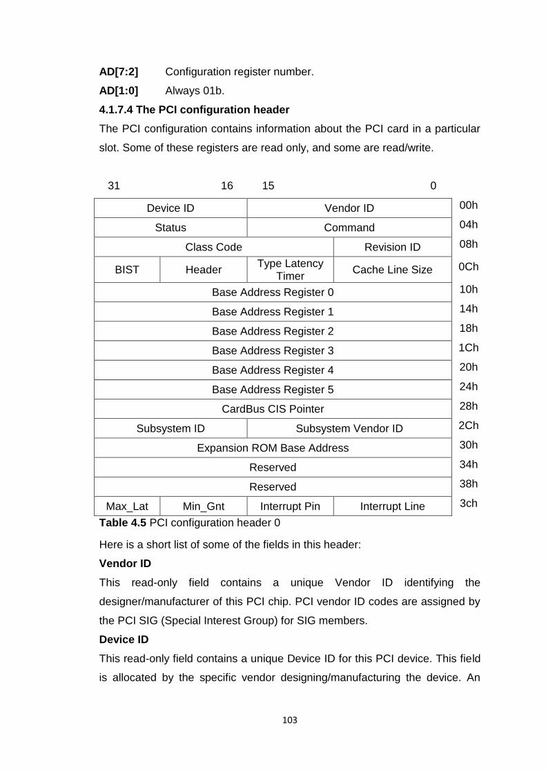
4.1.7.4 The PCI configuration header
The PCI configuration contains information about the PCI card in a particular
slot. Some of these registers are read only, and some are read/write.
31 16 15 0
Device ID Vendor ID 00h
Status Command 04h
Class Code Revision ID 08h
BIST Header Type Latency
Timer Cache Line Size 0Ch
Base Address Register 0 10h
Base Address Register 1 14h
Base Address Register 2 18h
Base Address Register 3 1Ch
Base Address Register 4 20h
Base Address Register 5 24h
CardBus CIS Pointer 28h
Subsystem ID Subsystem Vendor ID 2Ch
Expansion ROM Base Address 30h
Reserved 34h
Reserved 38h
Max_Lat Min_Gnt Interrupt Pin Interrupt Line 3ch
Table 4.5 PCI configuration header 0
Here is a short list of some of the fields in this header:
Vendor ID
This read-only field contains a unique Vendor ID identifying the
designer/manufacturer of this PCI chip. PCI vendor ID codes are assigned by
the PCI SIG (Special Interest Group) for SIG members.
Device ID
This read-only field contains a unique Device ID for this PCI device. This field
is allocated by the specific vendor designing/manufacturing the device. An
104
operating system could use the Device ID and Vendor ID fields to select a
specific device driver for this chip.
Command
This read/write field contains a 16 bit command register. Some of the bits in
this register are reserved, and some are optional. Bits which are not
implemented, must be read-only, and return 0 on read. Here is a short
explanation of all the different bits in this register in table 4.6.
Bit Location Description
0 I/O space enable. Writing 1 enables the device response to I/O space
access. Defaults to 0 after RST . If device has no I/O, this bit must be
hardwired to 0.
1 Memory space enable. Writing 1 enables the device response to
Memory space access. Defaults to 0 after RST . If the device is not
memory mapped, this bit must be hardwired to 0.
2 Master Enable. Writing 1 enables bus master behavior. Defaults to 0
after RST . If this is a target only device, this bit must be hardwired to
0.
3 Special Cycle Enable. Writing 1 enables response to special cycles.
Defaults to 0 after RST . If special cycles are not used, this bit must be
hardwired to 0.
4 MWI Enable. Writing 1 allows a bus master to use the Memory Write
and Invalidate command. Writing 0 forces the use of Memory Write
command. Defaults to 0 after RST . If the master does not support
MWI, this bit must be hardwired to 0.
5 VGA Palette snooping enable. When 1, device must snoop VGA
palette access (i.e. snoop data on bus, but do not respond). When 0,
treat like normal addresses. If device is not VGA compatible, this bit
must be hardwired to 0.
6 Parity error enable. When 0, Ignore parity errors. When 1, do normal
parity error action. If parity checking not supported, this bit must be
hardwired to 0. Devices that do not check for parity errors must still
generate correct parity.
7 Address/Data stepping enable. If device does address/data stepping,
105
this bit must be hardwires to 1. If device does not do address/data
stepping, this bit must be hardwires to 0. If device can optionally do
address/data stepping, this bit must be read/write, and default to 1
after RST ..
8 SERR Enable. When 1, SERR generation is enabled. When 0, no
SERR is generated. Defaults to 0 after RST . Can‘t be hardwired to 0
if SERR not supported.
9 Fast back to back Enable. When 1, master is allowed to generate fast
back to back cycles to different targets. When 0, master is allowed to
generate fast back to back cycles only to the same targets. This bit is
initialized by the BIOS to 1 if all targets are fast back-to-back capable.
Defaults to 0 after RST .
15:10 Reserved. Must return 0 on read.
Table 4.6 PCI Command configuration register
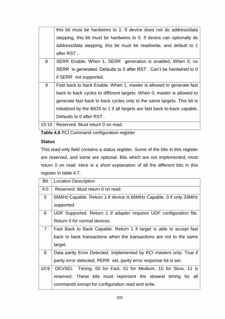
Status
This read-only field contains a status register. Some of the bits in this register
are reserved, and some are optional. Bits which are not implemented, must
return 0 on read. Here is a short explanation of all the different bits in this
register in table 4.7.
Bit Location Description
4:0 Reserved. Must return 0 on read.
5 66MHz Capable. Return 1 if device is 66MHz Capable, 0 if only 33MHz
supported.
6 UDF Supported. Return 1 if adapter requires UDF configuration file.
Return 0 for normal devices.
7 Fast Back to Back Capable. Return 1 if target is able to accept fast
back to back transactions when the transactions are not to the same
target.
8 Data parity Error Detected. Implemented by PCI masters only. True if
parity error detected, PERR set, parity error response bit is set.
10:9 DEVSEL Timing. 00 for Fast, 01 for Medium, 10 for Slow, 11 is
reserved. These bits must represent the slowest timing for all
commands except for configuration read and write.
106
11 Signaled Target Abort. Set by a target when it terminated a cycle with a
target abort.
12 Received Target Abort. Set by a master when it detected a cycle
ending with a target abort. All masters must implement this bit.
13 Received Master Abort. Set by a master when it detected a cycle
ending with a master abort. All masters must implement this bit.
14 Signaled System Error. Set if device asserted SERR . Must be
implemented only by device capable of generating SERR .
15 Detected parity Error. Set if parity error detected. Must be set on error
even if parity error handling (bit 6) is disabled.
Table 4.7 PCI Status configuration register
Revision ID
This read-only field contains a unique Revision ID for this PCI device. This
field is used to identify different versions of the same chip. For example, if
different revisions of the chip contained different bugs, a device driver
software could use the Revision ID field to select different workarounds to
bypass different chip bugs.
Class Code
This read-only field contains a field describing the device type. Some of the
device types identify specific types of devices which can then be programmed
by a generic device driver (for example, IDE interface, VGA card, PCI to PCI
bridge). Some other codes describe a device type, but still require a specific
device driver. (A SCSI controller, for example). For a list of class codes please
see Appendix .
Cache Line Size
This read/write field is filled by the BIOS or the operating system by the CPU
cache line size. This information is used by master and target devices if they
support burst transfers in cacheline wrap mode.
Latency Timer
This read/write field is used to initialize the PCI master latency timer. The
latency timer is initialized each time the PCI master device is granted the bus,
and begins a countdown when its GNT line is deasserted. When the latency
timer expires, the master must terminate its burst. This field can be read-only

107
for masters that does not support burst longer than two words, but must be
less than 16. Actually, not all the bits of this register must be implemented.
One or more bits (beginning with the least significant bit) can be made to
return 0 instead, reducing the timer‘s granularity.
Header Type
This read-only field contains a unique header type code in bits 6:0. Currently
defined values are 0 for the standard PCI header, 1 for PCI to PCI bridge
header, and 2 for PCI to CardBus bridge header. Header type codes of 3 and
above are reserved. The header type controls the layout of the configuration
addresses in the range 10h to 3Fh.
Bit 7 of the header type field specifies whether this device is a multi function
device. A value of 1 denotes a multi function device.
BIST
This read/write field controls Built-In Self Test for devices supporting this
feature. If not used, this field must contain 0.
Bit Name Name Description
7 BIST
Capable
Return 1 if device supports BIST, 0 otherwise.
6 Start BIST Write 1 to start BIST. Device will reset bit back to 0 when
BIST complete.
5:4 Reserved Must return 0
3:0 Completion Code Return 0 when completes with no errors. Non-zero
values are device specific errors.
Table 4.8 PCI BIST configuration register
Base Address Register 0 through Base Address Register 5
These read/write fields are initialized by the BIOS or operating system by
writing the desired base address where the PCI device is to be located in the
PCI memory map. A PCI device may use one or more base address registers.
CardBus CIS Pointer
This read-only field is used by devices which are both PCI and CardBus
compatible. It is used to point to the Card Information Structure for the
CardBus card. Subsystem Vendor ID, Subsystem ID These read-only fields
are used to identify a specific product using a generic PCI chip. This field can
be used by device drivers to take advantage of specific features in some
cards using generic PCI chips. Subsystem Vendor ID values are assigned by
108
the PCI SIG. Subsystem ID values are unique for every Subsystem Vendor
ID. This field is optional in PCI 2.1, but required according to Microsoft‘s PC97
and PCI 2.2 (to be released soon). It must contains 0 if not used. When
implemented by a PCI chip, there is usually a way to set this field externally,
most of the time through an external memory chip connected to the PCI
device. These way PCI board vendors can set this without making their own
PCI device.
Expansion ROM base Address
This is a special type of Base Address Register pointing to the card‘s
expansion ROM. Expansion ROMs are optional, and may contain additional
information about the card, boot code (in more than one executable format, as
well as the architecture independent OpenBoot format).
Interrupt Line
This read-write field is initialized by the BIOS or Operating system, and will
contain a system specific value identifying which hardware interrupt has been
assigned to this card. This value is not used by the card itself, but rather by
the driver and operating system which reads this field to determine which
interrupt vector has been assigned for the device. This field is not used by
devices not using interrupts.
Interrupt Pin
This read-only field defines which interrupt pin is used by this device. The
values contained this field are 1 to 4, corresponding to INTA to INTD .
Devices not using interrupts should put 0 in this field.
Min_Gnt, Max_Lat
These read-only fields are used by the BIOS to calculate the desired value for
the latency timer of this device. The Min Gnt field measures, in 250us units,
the minimum burst length this device requires. The Max_Lat field describes, in
250us units, how often the device requires access to the PCI Bus.
4.1.8 Basic PCI Cycles
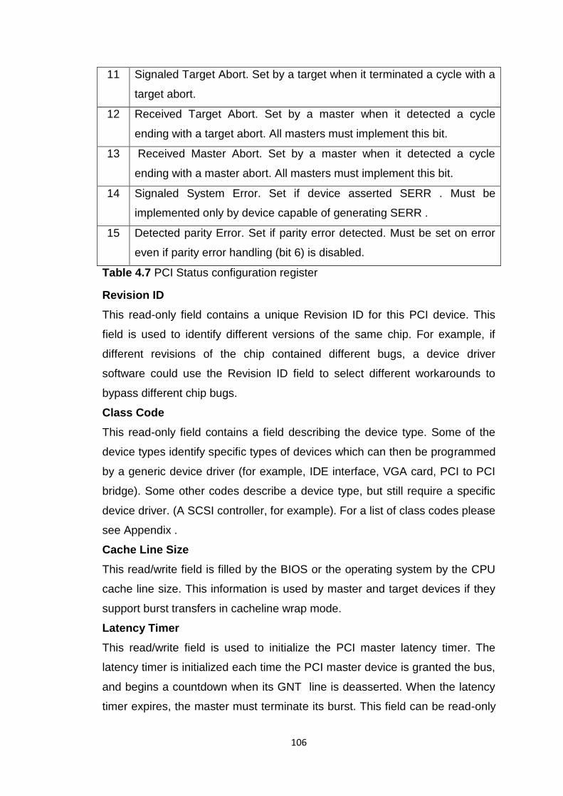
4.1.8.1 PCI Memory or I/O Read Cycle
The following timing diagram demonstrates a typical PCI memory or I/O burst
read transaction.
1. At Clock 0 the Master begins the transaction by driving FRAME low,
the requested address on AD[31:0], and the requested command on C/BE
109
[3:0] (I/O Read, Memory Read, Memory Read Line, or Memory Read
Multiple).
2. At Clock 1 the Target responds by asserting DEVSEL low. Since clock
1 is used for bus turnaround on read transaction (Master stops driving
AD[31:0], Target starts driving AD[31:0]), actual data transfer must begin
only on cycle 2, so TRDY and IRDY must be high, since no data is available
yet.
3. At clock 2 both IRDY and TRDY are low, so the 1st data word is read
(D0).
4. At clock 3 the Master is not ready to accept the new word, since IRDY
is high. The Target is ready to transfer the next word since TRDY is low.
Since not both are low, no data is transferred.
5. At clock 4 the master is able to receive data again, since IRDY is low,
and the 2nd data word is transferred. Since FRAME was high during this last
cycle, both the Master and the Target end the cycle.
6. At clock 5 the Target tri-states AD[31:0] (turnaround), and drives TRDY
high. The Master also drives IRDY high. This is done since IRDY and TRDY
are sustained-tri-state lines, and must be driven high for one cycle prior to tri-
stating them. This is done in order to charge the line, which will cause it to
stay at a high level even after it is tri stated.
Figure 4.5 PCI Memory and I/O read cycle
110
4.1.8.2 PCI Memory or I/O Write Cycle
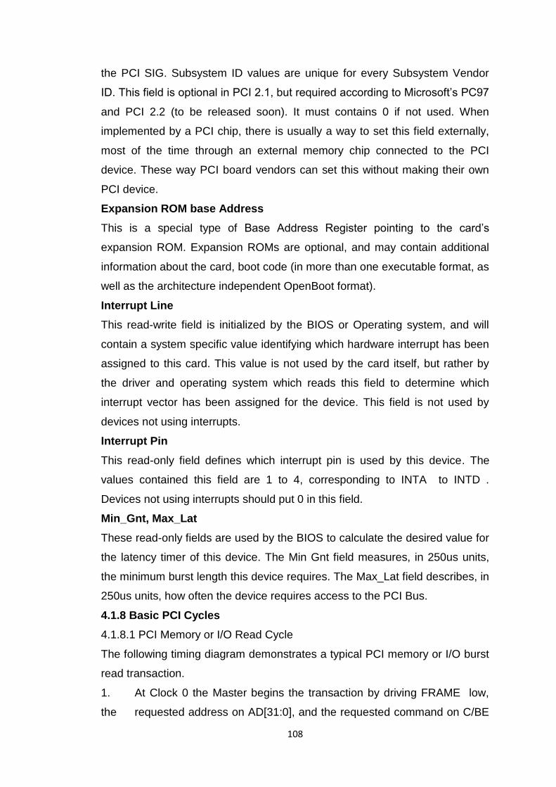
The following timing diagram demonstrates a typical PCI memory or I/O burst
read transaction.
1. At Clock 0 the Master begins the transaction by driving FRAME low,
the requested address on AD[31:0], and the requested command on C/BE
[3:0] (I/O Write, Memory Write, or Memory Write Line).
2. At Clock 1 the Target responds by asserting DEVSEL low. Since this is
a write transaction, the master keeps driving AD[31:0] (this time with
data), and no bus turnaround cycle is needed. IRDY is driven low to
indicate data is ready for write. Since the Target is driving TRDY high, it is not
ready to accept the data. C/BE [3:0] are loaded with the appropriate byte
enables.
3. At clock 2 both IRDY and TRDY are low, so the 1st data word is written
(D0).
4. At clock 3 the Master is not ready to send a new word (as indicated by
the invalid content of AD[31:0]), so IRDY is driven high. The Target is ready
to accept the next word since TRDY is low, but since IRDY is high, no data
transfer takes place.
5. At clock 4 the master is able to write data again, since IRDY is low,
and data is transferred. Since FRAME was high during this last cycle, both the
Master and the Target end the cycle.
6. At clock 5 the Target drives TRDY and DEVSEL high. The Master also
drives IRDY high. It may even start a new transaction right now (this is called
back to back transfers, when there are no turnaround cycles between multiple
transactions. Back-to-back transfers can only happen after a write transaction,
when no turnaround cycles are needed).
111
Figure 4.6 PCI Memory and I/O write cycle
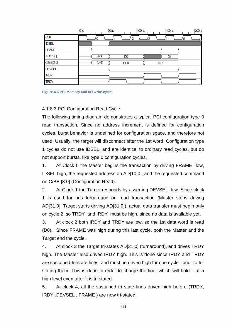
4.1.8.3 PCI Configuration Read Cycle
The following timing diagram demonstrates a typical PCI configuration type 0
read transaction. Since no address increment is defined for configuration
cycles, burst behavior is undefined for configuration space, and therefore not
used. Usually, the target will disconnect after the 1st word. Configuration type
1 cycles do not use IDSEL, and are identical to ordinary read cycles, but do
not support bursts, like type 0 configuration cycles.
1. At Clock 0 the Master begins the transaction by driving FRAME low,
IDSEL high, the requested address on AD[10:0], and the requested command
on C/BE [3:0] (Configuration Read).
2. At Clock 1 the Target responds by asserting DEVSEL low. Since clock
1 is used for bus turnaround on read transaction (Master stops driving
AD[31:0], Target starts driving AD[31:0]), actual data transfer must begin only
on cycle 2, so TRDY and IRDY must be high, since no data is available yet.
3. At clock 2 both IRDY and TRDY are low, so the 1st data word is read
(D0). Since FRAME was high during this last cycle, both the Master and the
Target end the cycle.
4. At clock 3 the Target tri-states AD[31:0] (turnaround), and drives TRDY
high. The Master also drives IRDY high. This is done since IRDY and TRDY
are sustained-tri-state lines, and must be driven high for one cycle prior to tri-
stating them. This is done in order to charge the line, which will hold it at a
high level even after it is tri stated.
5. At clock 4, all the sustained tri state lines driven high before (TRDY,
IRDY , DEVSEL , FRAME ) are now tri-stated.
112
Figure 4.7 PCI Configuration Read cycle
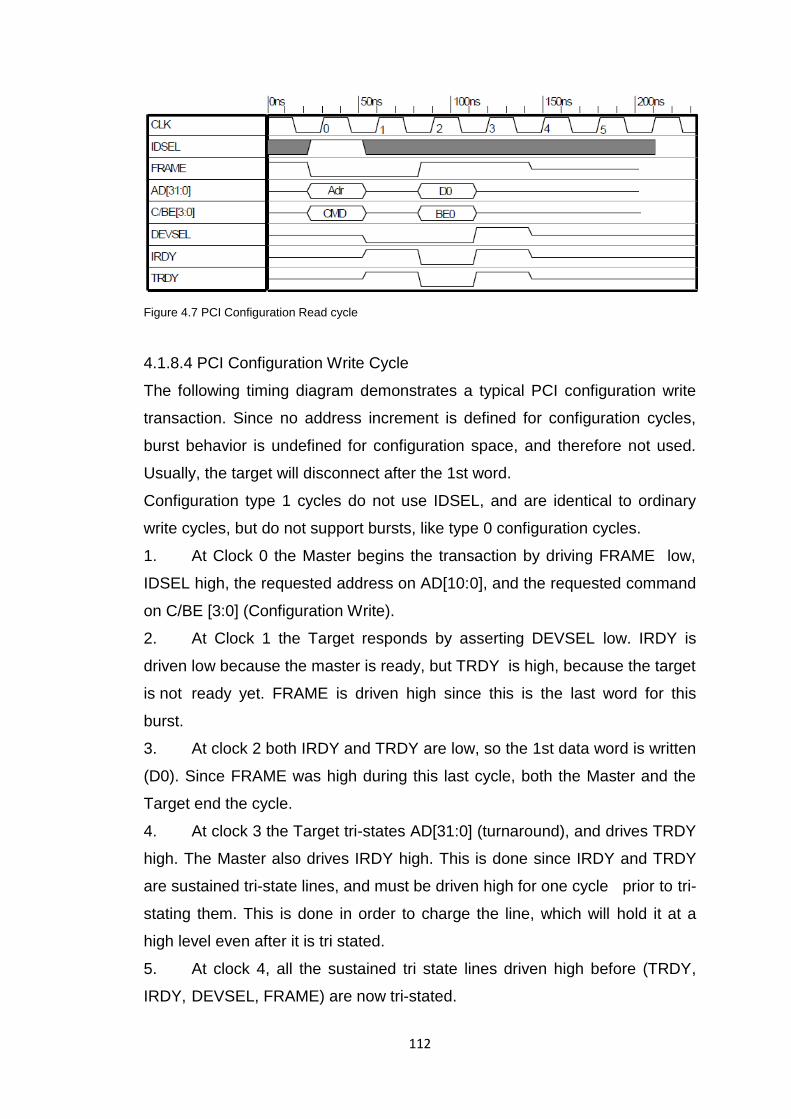
4.1.8.4 PCI Configuration Write Cycle
The following timing diagram demonstrates a typical PCI configuration write
transaction. Since no address increment is defined for configuration cycles,
burst behavior is undefined for configuration space, and therefore not used.
Usually, the target will disconnect after the 1st word.
Configuration type 1 cycles do not use IDSEL, and are identical to ordinary
write cycles, but do not support bursts, like type 0 configuration cycles.
1. At Clock 0 the Master begins the transaction by driving FRAME low,
IDSEL high, the requested address on AD[10:0], and the requested command
on C/BE [3:0] (Configuration Write).
2. At Clock 1 the Target responds by asserting DEVSEL low. IRDY is
driven low because the master is ready, but TRDY is high, because the target
is not ready yet. FRAME is driven high since this is the last word for this
burst.
3. At clock 2 both IRDY and TRDY are low, so the 1st data word is written
(D0). Since FRAME was high during this last cycle, both the Master and the
Target end the cycle.
4. At clock 3 the Target tri-states AD[31:0] (turnaround), and drives TRDY
high. The Master also drives IRDY high. This is done since IRDY and TRDY
are sustained tri-state lines, and must be driven high for one cycle prior to tri-
stating them. This is done in order to charge the line, which will hold it at a
high level even after it is tri stated.
5. At clock 4, all the sustained tri state lines driven high before (TRDY,
IRDY, DEVSEL, FRAME) are now tri-stated.
113
Figure 4.8 PCI Configuration Write cycle
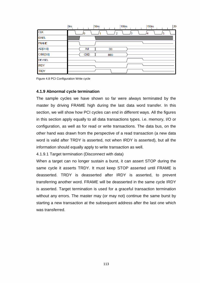
4.1.9 Abnormal cycle termination
The sample cycles we have shown so far were always terminated by the
master by driving FRAME high during the last data word transfer. In this
section, we will show how PCI cycles can end in different ways. All the figures
in this section apply equally to all data transactions types. i.e. memory, I/O or
configuration, as well as for read or write transactions. The data bus, on the
other hand was drawn from the perspective of a read transaction (a new data
word is valid after TRDY is asserted, not when IRDY is asserted), but all the
information should equally apply to write transaction as well.
4.1.9.1 Target termination (Disconnect with data)
When a target can no longer sustain a burst, it can assert STOP during the
same cycle it asserts TRDY. It must keep STOP asserted until FRAME is
deasserted. TRDY is deasserted after IRDY is asserted, to prevent
transferring another word. FRAME will be deasserted in the same cycle IRDY
is asserted. Target termination is used for a graceful transaction termination
without any errors. The master may (or may not) continue the same burst by
starting a new transaction at the subsequent address after the last one which
was transferred.
114
Figure 4.9 Target Disconnect with data
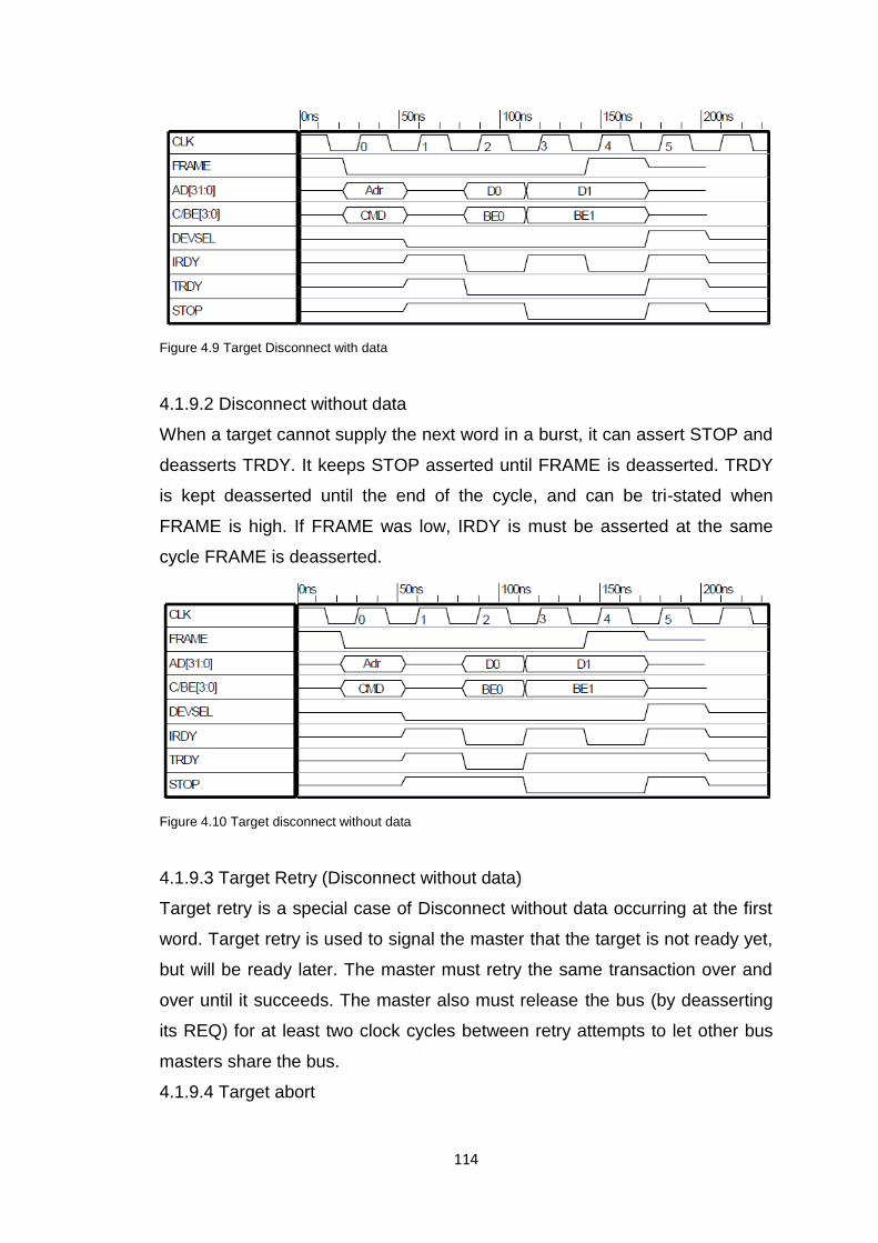
4.1.9.2 Disconnect without data
When a target cannot supply the next word in a burst, it can assert STOP and
deasserts TRDY. It keeps STOP asserted until FRAME is deasserted. TRDY
is kept deasserted until the end of the cycle, and can be tri-stated when
FRAME is high. If FRAME was low, IRDY is must be asserted at the same
cycle FRAME is deasserted.
Figure 4.10 Target disconnect without data
4.1.9.3 Target Retry (Disconnect without data)
Target retry is a special case of Disconnect without data occurring at the first
word. Target retry is used to signal the master that the target is not ready yet,
but will be ready later. The master must retry the same transaction over and
over until it succeeds. The master also must release the bus (by deasserting
its REQ) for at least two clock cycles between retry attempts to let other bus
masters share the bus.
4.1.9.4 Target abort
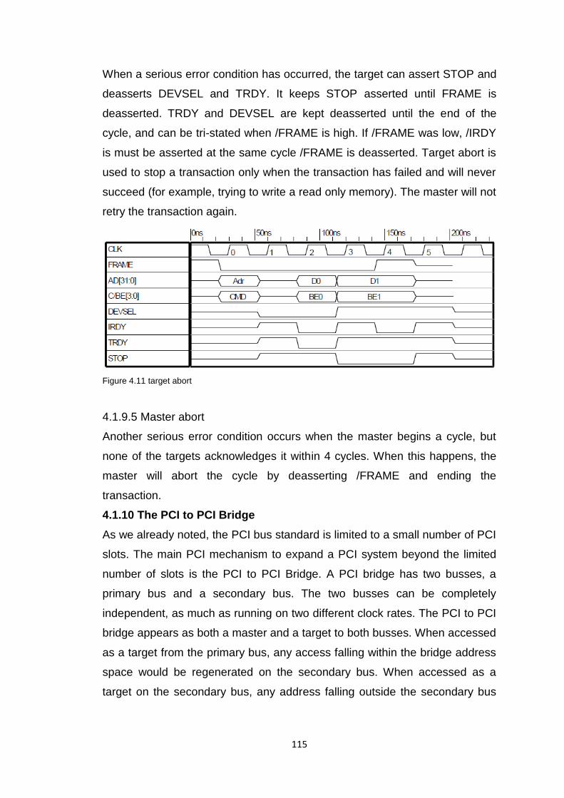
115
When a serious error condition has occurred, the target can assert STOP and
deasserts DEVSEL and TRDY. It keeps STOP asserted until FRAME is
deasserted. TRDY and DEVSEL are kept deasserted until the end of the
cycle, and can be tri-stated when /FRAME is high. If /FRAME was low, /IRDY
is must be asserted at the same cycle /FRAME is deasserted. Target abort is
used to stop a transaction only when the transaction has failed and will never
succeed (for example, trying to write a read only memory). The master will not
retry the transaction again.
Figure 4.11 target abort
4.1.9.5 Master abort
Another serious error condition occurs when the master begins a cycle, but
none of the targets acknowledges it within 4 cycles. When this happens, the
master will abort the cycle by deasserting /FRAME and ending the
transaction.
4.1.10 The PCI to PCI Bridge
As we already noted, the PCI bus standard is limited to a small number of PCI
slots. The main PCI mechanism to expand a PCI system beyond the limited
number of slots is the PCI to PCI Bridge. A PCI bridge has two busses, a
primary bus and a secondary bus. The two busses can be completely
independent, as much as running on two different clock rates. The PCI to PCI
bridge appears as both a master and a target to both busses. When accessed
as a target from the primary bus, any access falling within the bridge address
space would be regenerated on the secondary bus. When accessed as a
target on the secondary bus, any address falling outside the secondary bus
116
address range would be regenerated on the primary bus. Notice that the
secondary bus will not respond to configuration type 0 commands.
Very large PCI systems may have up to 255 busses arranged this way. The
PCI to PCI Bridge has a slightly different configuration header, called header
type 1. The header structure, as well as the register description is listed
below. PCI to PCI Bridge are complex devices and we cannot cover all their
functions. For a complete specifications of the PCI to PCI Bridge devices,
please refer to [3].
4.2 AVR 8 – bit Microcontroller family.
The AVR enhanced RISC microcontrollers [1] are based on a new RISC
architecture that has been developed to take advantage of semiconductor
integration and software capabilities of the 1990's. The AVR is a family of
RISC microcontrollers from Atmel. The AVR architecture, first conceived by
two electronic engineering students at the Norwegian Institute of Technology
(NTH), has been refined and developed by Atmel Norway, in a division
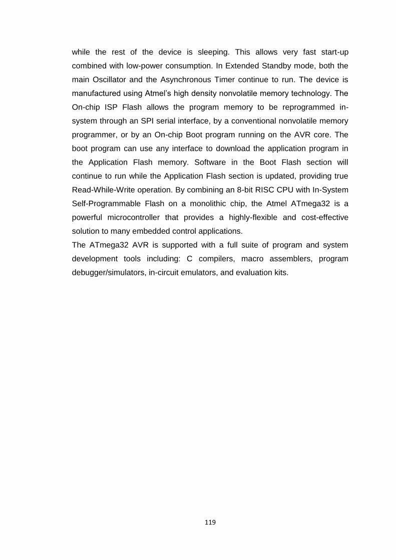
founded by the chip's architects. A block diagram of the AVR architecture is
given in figure 4.14. The memory sizes and peripherals indicated in the figure
4.12 are for the ATmega32 microcontroller.
The key benefits of AVR family of microcontrollers are:
High performance.
Low power consumption.
High code density.
Outstanding memory technology.
High integration.
The main purpose to use AVR is the scalability of the family. The devices
ranges from 1to 256KB, pin count ranges from 8 to 100, full code
compatibility, pin/feature compatible family and single set of development
tools. Any member is either a subset or superset of other family members of
the AVR microcontroller family.
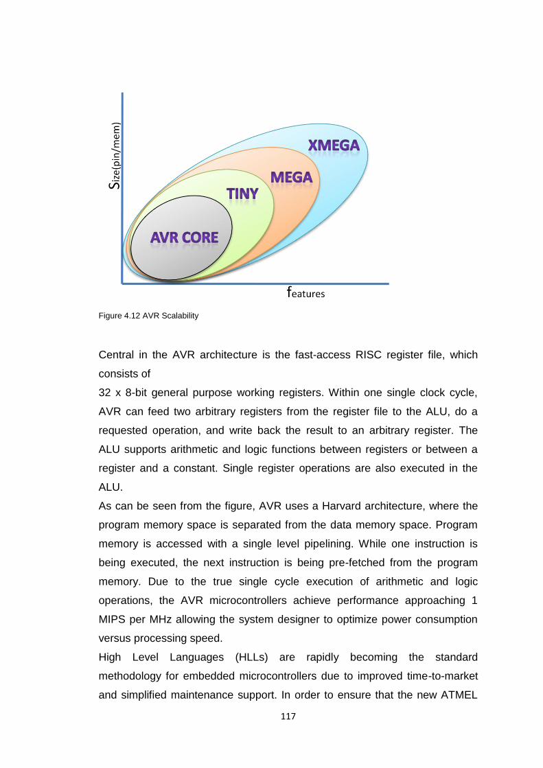
117
Figure 4.12 AVR Scalability
Central in the AVR architecture is the fast-access RISC register file, which
consists of
32 x 8-bit general purpose working registers. Within one single clock cycle,
AVR can feed two arbitrary registers from the register file to the ALU, do a
requested operation, and write back the result to an arbitrary register. The
ALU supports arithmetic and logic functions between registers or between a
register and a constant. Single register operations are also executed in the
ALU.
As can be seen from the figure, AVR uses a Harvard architecture, where the
program memory space is separated from the data memory space. Program
memory is accessed with a single level pipelining. While one instruction is
being executed, the next instruction is being pre-fetched from the program
memory. Due to the true single cycle execution of arithmetic and logic
operations, the AVR microcontrollers achieve performance approaching 1
MIPS per MHz allowing the system designer to optimize power consumption
versus processing speed.
High Level Languages (HLLs) are rapidly becoming the standard
methodology for embedded microcontrollers due to improved time-to-market
and simplified maintenance support. In order to ensure that the new ATMEL
118
AVR family of microcontrollers was well suited as a target for C compiler, the
external C compiler development was started before the AVR architecture and
instruction set were completed. During the initial development of the C
compiler, several potential improvements in the AVR were identified and
implemented. The result of this cooperation between the compiler developer
and the AVR development team is a microcontroller for which highly efficient,
high performance code is generated.
About ATmega32
The AVR core combines a rich instruction set with 32 general purpose
working registers. All the 32 registers are directly connected to the Arithmetic
Logic Unit (ALU), allowing two independent registers to be accessed in one
single instruction executed in one clock cycle. The resulting architecture is
more code efficient while achieving throughputs up to ten times faster than
conventional CISC microcontrollers.
The ATmega32 provides the following features: 32K bytes of In-System
Programmable Flash Program memory with Read-While-Write capabilities,
1024 bytes EEPROM, 2K byte SRAM, 32 general purpose I/O lines, 32
general purpose working registers, a JTAG interface for Boundary-scan, On-
chip Debugging support and programming, three flexible Timer/Counters with
compare modes, Internal and External Interrupts, a serial programmable
USART, a byte oriented Two-wire Serial Interface, an 8-channel, 10-bit ADC
with optional differential input stage with programmable gain (TQFP package
only), a programmable Watchdog Timer with Internal Oscillator, an SPI serial
port, and six software selectable power saving modes. The Idle mode stops
the CPU while allowing the USART, Two-wire interface, A/D Converter,
SRAM, Timer/Counters, SPI port, and interrupt system to continue
functioning. The Power-down mode saves the register contents but freezes
the Oscillator, disabling all other chip functions until the next External Interrupt
or Hardware Reset. In Power-save mode, the Asynchronous Timer continues
to run, allowing the user to maintain a timer base while the rest of the device
is sleeping.
The ADC Noise Reduction mode stops the CPU and all I/O modules except
Asynchronous Timer and ADC, to minimize switching noise during ADC
conversions. In Standby mode, the crystal/resonator Oscillator is running
119
while the rest of the device is sleeping. This allows very fast start-up
combined with low-power consumption. In Extended Standby mode, both the
main Oscillator and the Asynchronous Timer continue to run. The device is
manufactured using Atmel‘s high density nonvolatile memory technology. The
On-chip ISP Flash allows the program memory to be reprogrammed in-
system through an SPI serial interface, by a conventional nonvolatile memory
programmer, or by an On-chip Boot program running on the AVR core. The
boot program can use any interface to download the application program in
the Application Flash memory. Software in the Boot Flash section will
continue to run while the Application Flash section is updated, providing true
Read-While-Write operation. By combining an 8-bit RISC CPU with In-System
Self-Programmable Flash on a monolithic chip, the Atmel ATmega32 is a
powerful microcontroller that provides a highly-flexible and cost-effective
solution to many embedded control applications.
The ATmega32 AVR is supported with a full suite of program and system
development tools including: C compilers, macro assemblers, program
debugger/simulators, in-circuit emulators, and evaluation kits.
120
Figure 4.13 Block Diagram of ATmega32
121
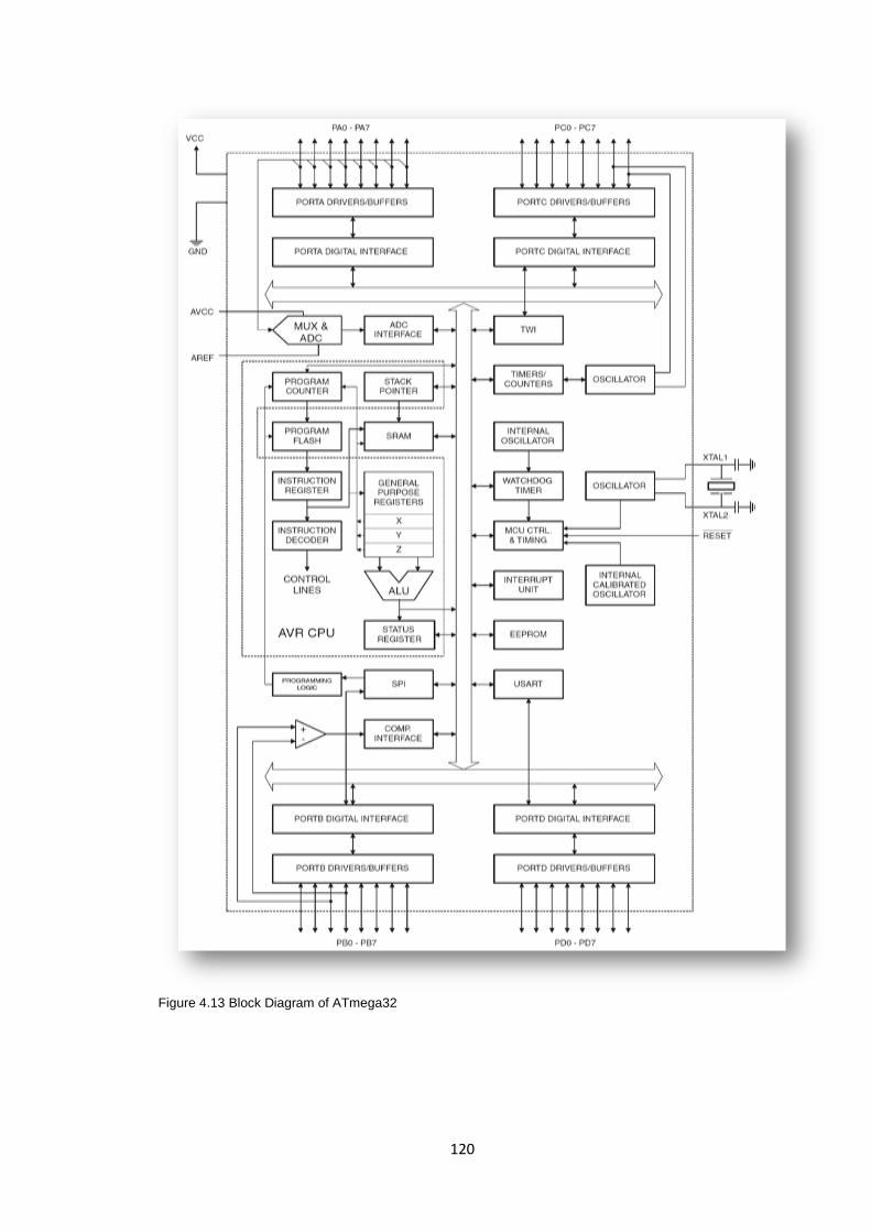
Figure 4.14 Pinout of ATmega32
AVR CPU Core
Introduction This section discusses the AVR core architecture in general.
The main function of the CPU core is to ensure correct program execution.
The CPU must therefore be able to access memories, perform calculations,
control peripherals, and handle interrupt
Architectural Overview
In order to maximize performance and parallelism, the AVR uses a Harvard
architecture with separate memories and buses for program and data.
Instructions in the program memory are executed with a single level
pipelining. While one instruction is being executed, the next instruction is pre-
fetched from the program memory. This concept enables instructions to be
executed in every clock cycle. The program memory is In-System
Reprogrammable Flash memory.
The fast-access Register File contains 32 x 8-bit general purpose working
registers with a single clock cycle access time. This allows single-cycle
Arithmetic Logic Unit (ALU) operation. In a typical ALU operation, two
operands are output from the Register File, the operation is executed, and the
result is stored back in the Register File – in one clock cycle.
Six of the 32 registers can be used as three 16-bit indirect address register
pointers for
Data Space addressing – enabling efficient address calculations. One of
these address pointers can also be used as an address pointer for look up
122
tables in Flash Program memory. These added function registers are the 16-
bit X-, Y-, and Z-register, described later in this section.
The ALU supports arithmetic and logic operations between registers or
between a constant and a register. Single register operations can also be
executed in the ALU. After an arithmetic operation, the Status Register is
updated to reflect information about the result of the operation.
Program flow is provided by conditional and unconditional jump and call
instructions, able to directly address the whole address space. Most AVR
instructions have a single 16-bit word format. Every program memory address
contains a 16- or 32-bit instruction.
Program Flash memory space is divided in two sections, the Boot program
section and the Application Program section. Both sections have dedicated
Lock bits for write and read/write protection. The SPM instruction that writes
into the Application Flash memory section must reside in the Boot Program
section.
During interrupts and subroutine calls, the return address Program Counter
(PC) is stored on the Stack. The Stack is effectively allocated in the general
data SRAM, and consequently the Stack size is only limited by the total
SRAM size and the usage of the SRAM. All user programs must initialize the
SP in the reset routine (before subroutines or interrupts are executed). The
Stack Pointer SP is read/write accessible in the I/O space. The data SRAM
can easily be accessed through the five different addressing modes supported
in the AVR architecture.
The memory spaces in the AVR architecture are all linear and regular memory
maps. A flexible interrupt module has its control registers in the I/O space with
an additional global interrupt enable bit in the Status Register. All interrupts
have a separate interrupt vector in the interrupt vector table. The interrupts
have priority in accordance with their interrupt vector position. The lower the
interrupt vector address, the higher the priority.
The I/O memory space contains 64 addresses for CPU peripheral functions
as Control Registers, SPI, and other I/O functions. The I/O Memory can be
accessed directly, or as the Data Space locations following those of the
Register File, $20 - $5F.

123
Figure 4.15 Block Diagram of the AVR MCU Architecture
JTAG Interface and On-chip Debug System
Features
• JTAG (IEEE std. 1149.1 Compliant) Interface
• Boundary-scan Capabilities According to the IEEE std. 1149.1 (JTAG)
Standard
• Debugger Access to:
– All Internal Peripheral Units
– Internal and External RAM
– The Internal Register File
– Program Counter
– EEPROM and Flash Memories
– Extensive On-chip Debug Support for Break Conditions, Including
– AVR Break Instruction
– Break on Change of Program Memory Flow
– Single Step Break
124
– Program Memory Breakpoints on Single Address or Address Range
– Data Memory Breakpoints on Single Address or Address Range
• Programming of Flash, EEPROM, Fuses, and Lock Bits through the JTAG
Interface
• On-chip Debugging Supported by AVR Studio®
Overview The AVR IEEE std. 1149.1 compliant JTAG interface can be used
for
• Testing PCBs by using the JTAG Boundary-scan capability
• Programming the non-volatile memories Fuses and Lock bits
• On-chip Debugging
Boot Loader Support – Read-While-Write Self-Programming
The Boot Loader Support provides a real Read-While-Write Self-Programming
mechanism for downloading and uploading program code by the MCU itself.
This feature allows flexible application software updates controlled by the
MCU using a Flash-resident Boot Loader program. The Boot Loader program
can use any available data interface and associated protocol to read code and
write (program) that code into the Flash memory, or read the code from the
Program memory. The program code within the Boot Loader section has the
capability to write into the entire Flash, including the Boot Loader memory.
The Boot Loader can thus even modify itself, and it can also erase itself from
the code if the feature is not needed anymore. The size of the Boot Loader
memory is configurable with Fuses and the Boot Loader has two separate
sets of Boot Lock bits which can be set independently. This gives the user a
unique flexibility to select different levels of protection.
Features
• Read-While-Write Self-Programming
• Flexible Boot Memory size
• High Security (Separate Boot Lock Bits for a Flexible Protection)
• Separate Fuse to Select Reset Vector
• Optimized Page(1) Size
• Code Efficient Algorithm
• Efficient Read-Modify-Write Support
The Instruction set of AVR microcontroller is included in the Appendix.
125
4.3 PCI Interfacing Chip (MCS9835CV)
The MCS9835 is a PCI based dual-channel high performance UART with
enhanced bi-directional parallel controller. The MCS9835 offers 16-Byte
transmit and receive FIFOs for each UART channel and a 16-Byte FIFO for
the printer channel. The MCS9835 performs serial-to-parallel conversions on
data received from a peripheral device, and parallel-to-serial conversions on
data received from its CPU. In addition, MCS9835 fully supports the existing
Centronics printer interface as well as PS/2, EPP, and ECP modes.
The MCS9835 is ideally suited for PC applications, such as high speed COM
ports and parallel ports. The MCS9835 is available in a 128-pin QFP package.
It is fabricated using an advanced submicron CMOS process to achieve low
drain power and high-speed requirements.
The MCS9835 can be used in both 3.3V and 5V PCI signaling environments.
The MCS9835 is a pin-compatible replacement for the previous Nm9835. The
Nm9835 is no longer offered. It was only warranted for use with a 5V power
supply, and was only intended to operate in 5V PCI signaling environments.
The MCS9835‘s new RoHS ―Lead Free‖ package and 3.3V or 5V operation
make it a much more flexible device that is better suited for new designs.

126
Figure 4.16 Block diagram of MCS9835CV
PCI Bus Operation:
The execution of PCI Bus transactions take place in broadly five stages:
address phase; transaction claiming; data phase(s); final data transfer; and
transaction completion.
Address Phase:
Every PCI transaction starts with an address phase, one PCI clock period in
duration. During the address phase the initiator (also known as the current
Bus Master) identifies the target device (via the address) and type of
transaction (via the command). The initiator drives the 32-bit address onto the
Address/Data Bus, and a 4-bit command onto the Command/Byte-Enable
Bus. The initiator also asserts the /FRAME signal during the same clock cycle
to indicate the presence of valid address and transaction information on those
buses. The initiator supplies the starting address and command type for one
PCI clock cycle. The target generates the subsequent sequential addresses
127
for burst transfers. The Address/Data Bus becomes the Data Bus, and the
Command/Byte-Enable Bus becomes the Byte-Enable Bus for the remainder
of the clock cycles in that transaction. The target latches the address and
command type on the next rising edge of PCI clock, as do all other devices on
that PCI bus. Each device then decodes the address and determines whether
it is the intended target, and also decodes the command to determine the type
of transaction.
Claiming the Transaction:
When a device determines that it is the target of a transaction, it claims the
transaction by asserting /DEVSEL.
Data Phase(s):
The data phase of a transaction is the period during which a data object is
transferred between the initiator and the target. The number of data Bytes to
be transferred during a data phase is determined by the number of
Command/Byte-Enable signals that are asserted by the initiator during the
data phase. Each data phase is at least one PCI clock period in duration. Both
initiator and target must indicate that they are ready to complete a data phase.
If not, the data phase is extended by a wait state of one clock period in
duration. The initiator and the target indicate this by asserting /IRDY and
/TRDY respectively and the data transfer is completed at the rising edge of
the next PCI clock.
Transaction Duration:
The initiator, as stated earlier, gives only the starting address during the
address phase. It does not tell the number of data transfers in a burst transfer
transaction. The target will automatically generate the addresses for
subsequent Data Phase transfers. The initiator indicates the completion of a
transaction by asserting /IRDY and de-asserting /FRAME during the last data
transfer phase. The transaction does not actually complete until the target has
also asserted the /TRDY signal and the last data transfer takes place. At this
point the /TRDY and /DEVSEL are de-asserted by the target.
Transaction Completion:
When all of nIRDY, nTRDY, nDEVSEL, and nFRAME are in the inactive state
(high state), the bus is in idle state. The bus is then ready to be claimed by
another Bus Master.
128
PCI Resource Allocation
PCI devices do not have ―Hard-Wired‖ assignments for memory or I/O Ports
like ISA devices do. PCI devices use ―Plug & Play‖ to obtain the required
resources each time the system boots up. Each PCI device can request up to
six resource allocations. These can be blocks of memory (RAM) or blocks of
I/O Registers. The size of each resource block requested can also be
specified, allowing great flexibility. Each of these resource blocks is accessed
by means of a Base- Address-Register (BAR). As the name suggests, this is a
pointer to the start of the resource. Individual registers are then addressed
using relative offsets from the Base-Address-Register contents. The important
thing to note is: plugging the same PCI card into different machines will not
necessarily result in the same addresses being assigned to it. For this reason,
software (drivers, etc.) must always obtain the specific addresses for the
device from the PCI System. Each PCI device is assigned an entry in the PCI
System‘s shared ―Configuration Space‖. Every device is allocated 256 Bytes
in the Configuration Space. The first 64 Bytes must follow the conventions of
a standard PCI Configuration ―Header‖. There are several pieces of
information the device must present in specific fields within the header to
allow the PCI System to properly identify it. These include the Vendor-ID,
Device-ID and Class-Code. These three fields should provide enough
information to allow the PCI System to associate the correct software driver
with the hardware device. Other fields can be used to provide additional
information to further refine the needs and capabilities of the device. As part
of the Enumeration process (discovery of which devices are present in the
system) the Base- Address-Registers are configured for each device. The
device tells the system how many registers (etc.) it requires, and the system
maps that number into the system‘s resource space, reserving them for
exclusive use by that particular device. No guarantees are made that any two
requests for resources will have any predictable relationship to each other.
Each PCI System is free to use its own allocation strategy when managing
resources.
For detail information the datasheet attached may be referred.
129
4.4 Microcontroller Programming Protocols – SPI and JTAG.
The microcontrollers have programmable flash memory and EEPROM
memory that can be programmed using common techniques mentioned
below:
Programming Interfaces
In System Programming (ISP)
High Voltage Serial Programming (HVSP)
Parallel Programming (PP)
JTAG Programming (JTAG Prog)
PDI Programming on selected devices (PDI)
Debuging Interfaces
JTAG (JTAG)
debugWIRE (dW)
PDI on selected devices (PDI)
All of the above mentioned have different physical and logical
implementations. The Flash program memories, boot code memory,
EEPROM memory, fuse bits, lock protection bits can only be programmed
using the above techniques. The AVR microcontrollers have programmable
flash memory and EEPROM that can be programmed while it is in the product
using ISP technique. This is called In System Programming technique. Also
they can also be programmed with the firmware running inside them, while the
product is running is normal application. This is called In Application
Programming technique.
For programming the AVR we require application software that will take the
user input, one programming system to program the AVR with computer
interface and the target AVR.
For example, take AVR Studio software for user input, AVR Dragon as
programmer/debugger and ATmega128 as target microcontroller. At present,
the PCI card is developed to be using JTAG interface for programming and
debugging, detail discussion about JTAG physical and logical extension is
given and short discussion about SPI programming is also described.
130
4.4.1 JTAG Interface
JTAG is commonly used to debug embedded systems and to program
hardware devices. Companies like Atmel often provide JTAG interfaces on
their products because of its popularity in industry. The full form of JTAG is
Joint Test Action Group, the team of over 200 software companies, test and
system vendor started in mid 80‘s. The standard was sanctioned by IEEE as
Std. 1149.1 Test Access Port and Boundary Scan Architecture in 1990. The
main focus of this standard was to build test facilities and testing points into
chips and ensure compatibility among the compatible ICs.
Figure 4.16 shows a block diagram of the JTAG interface and the On-chip
Debug system including TAP Controller. The TAP Controller is a 16 state
machine controlled by the TCK and TMS signals and controls the operation of
Boundary scan circuitry, JTAG programming circuitry, or On-chip Debug
system. The TAP Controller selects either the JTAG Instruction Register or
one of several Data Registers as the scan chain (Shift Register) between the
TDI input and TDO output. The Instruction Register holds JTAG instructions
controlling the behavior of a Data Register. The ID-Register, Bypass Register,
and the Boundary-scan Chain are the Data Registers used for board-level
testing. The JTAG Programming Interface (actually consisting of several
physical and virtual Data Registers) is used for JTAG Serial Programming via
the JTAG interface. The Internal Scan Chain and Break Point Scan Chain are
used for On-chip Debugging only.

131
Figure 4.17 Block Diagram of JTAG peripheral in AVR(from datasheet).
The JTAG interface is accessed through four of the AVR‘s pins. In JTAG
terminology, these pins constitute the Test Access Port – TAP. These pins
are:
TMS: Test Mode Select. This pin is used for navigating through the TAP-
controller state machine.
TCK: Test Clock. JTAG operation is synchronous to TCK.
TDI: Test Data In. Serial input data to be shifted in to the Instruction Register
or Data Register (Scan Chains).
TDO: Test Data Out. Serial output data from Instruction register or Data
Register.
The state transitions depicted in Figure 4.17 depend on the signal present on
TMS (shown adjacent to each state transition) at the time of the rising edge at
TCK. The initial state after a Power-On Reset is Test-Logic-Reset. The LSB is
shifted in and out first for all Shift Registers.
132
Assuming Run-Test/Idle is the present state, a typical scenario for using the
JTAG interface is:
1. At the TMS input, apply the sequence 1, 1, 0, 0 at the rising edges of
TCK to enter the Shift Instruction Register – Shift-IR state. While in this state,
shift the four bits of the JTAG instructions into the JTAG Instruction Register
from the TDI input at the rising edge of TCK. The TMS input must be held low
during input of the 3 LSBs in order to remain in the Shift-IR state. The MSB of
the instruction is shifted in when this state is left by setting TMS high. While
the instruction is shifted in from the TDI pin, the captured IR-state 0x01 is
shifted out on the TDO pin. The JTAG Instruction selects a particular Data
Register as path between TDI and TDO and controls the circuitry surrounding
the selected Data Register.
2. Apply the TMS sequence 1, 1, 0 to re-enter the Run-Test/Idle state.
The instruction is latched onto the parallel output from the Shift Register path
in the Update-IR state. The Exit-IR, Pause-IR, and Exit2-IR states are only
used for navigating the state machine.
3. At the TMS input, apply the sequence 1, 0, 0 at the rising edges of
TCK to enter the Shift Data Register – Shift-DR state. While in this state,
upload the selected Data Register (selected by the present JTAG instruction
in the JTAG Instruction Register) from the TDI input at the rising edge of TCK.
In order to remain in the Shift-DR state, the TMS input must be held low
during input of all bits except the MSB. The MSB of the data is shifted in when
this state is left by setting TMS high. While the Data Register is shifted in from
the TDI pin, the parallel inputs to the Data Register captured in the Capture-
DR state is shifted out on the TDO pin.
4. Apply the TMS sequence 1, 1, 0 to re-enter the Run-Test/Idle state. If the
selected Data Register has a latched parallel-output, the latching takes place
in the Update-DR state. The Exit-DR, Pause-DR, and Exit2-DR states are
only used for navigating the state machine.
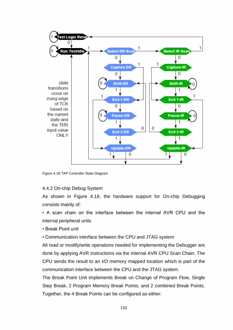
133
Figure 4.18 TAP Controller State Diagram
4.4.2 On-chip Debug System
As shown in Figure 4.18, the hardware support for On-chip Debugging
consists mainly of:
• A scan chain on the interface between the internal AVR CPU and the
internal peripheral units
• Break Point unit
• Communication interface between the CPU and JTAG system
All read or modify/write operations needed for implementing the Debugger are
done by applying AVR instructions via the internal AVR CPU Scan Chain. The
CPU sends the result to an I/O memory mapped location which is part of the
communication interface between the CPU and the JTAG system.
The Break Point Unit implements Break on Change of Program Flow, Single
Step Break, 2 Program Memory Break Points, and 2 combined Break Points.
Together, the 4 Break Points can be configured as either:
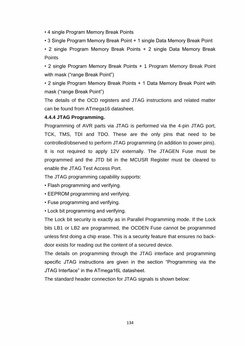
134
• 4 single Program Memory Break Points
• 3 Single Program Memory Break Point + 1 single Data Memory Break Point
• 2 single Program Memory Break Points + 2 single Data Memory Break
Points
• 2 single Program Memory Break Points + 1 Program Memory Break Point
with mask (―range Break Point‖)
• 2 single Program Memory Break Points + 1 Data Memory Break Point with
mask (―range Break Point‖)
The details of the OCD registers and JTAG instructions and related matter
can be found from ATmega16 datasheet.
4.4.4 JTAG Programming.
Programming of AVR parts via JTAG is performed via the 4-pin JTAG port,
TCK, TMS, TDI and TDO. These are the only pins that need to be
controlled/observed to perform JTAG programming (in addition to power pins).
It is not required to apply 12V externally. The JTAGEN Fuse must be
programmed and the JTD bit in the MCUSR Register must be cleared to
enable the JTAG Test Access Port.
The JTAG programming capability supports:
• Flash programming and verifying.
• EEPROM programming and verifying.
• Fuse programming and verifying.
• Lock bit programming and verifying.
The Lock bit security is exactly as in Parallel Programming mode. If the Lock
bits LB1 or LB2 are programmed, the OCDEN Fuse cannot be programmed
unless first doing a chip erase. This is a security feature that ensures no back-
door exists for reading out the content of a secured device.
The details on programming through the JTAG interface and programming
specific JTAG instructions are given in the section ―Programming via the
JTAG Interface‖ in the ATmega16L datasheet.
The standard header connection for JTAG signals is shown below:
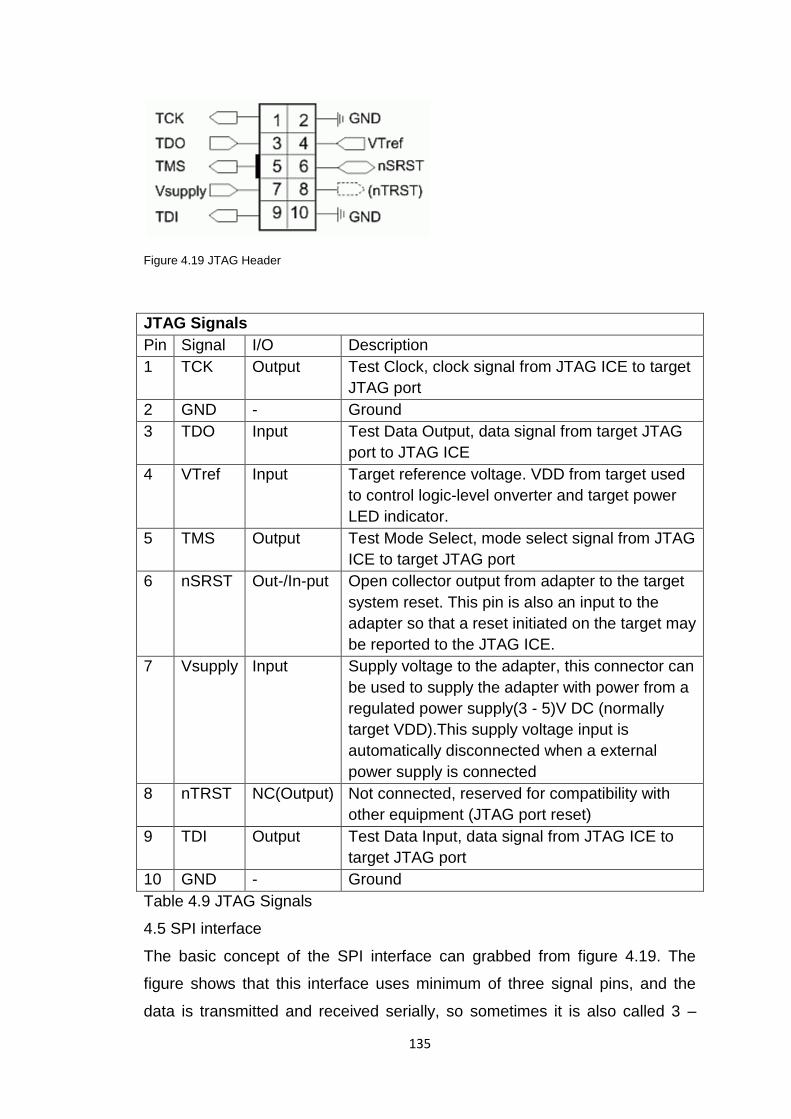
135
Figure 4.19 JTAG Header
JTAG Signals
Pin Signal I/O Description
1 TCK Output Test Clock, clock signal from JTAG ICE to target
JTAG port
2 GND - Ground
3 TDO Input Test Data Output, data signal from target JTAG
port to JTAG ICE
4 VTref Input Target reference voltage. VDD from target used
to control logic-level onverter and target power
LED indicator.
5 TMS Output Test Mode Select, mode select signal from JTAG
ICE to target JTAG port
6 nSRST Out-/In-put Open collector output from adapter to the target
system reset. This pin is also an input to the
adapter so that a reset initiated on the target may
be reported to the JTAG ICE.
7 Vsupply Input Supply voltage to the adapter, this connector can
be used to supply the adapter with power from a
regulated power supply(3 - 5)V DC (normally
target VDD).This supply voltage input is
automatically disconnected when a external
power supply is connected
8 nTRST NC(Output) Not connected, reserved for compatibility with
other equipment (JTAG port reset)
9 TDI Output Test Data Input, data signal from JTAG ICE to
target JTAG port
10 GND - Ground
Table 4.9 JTAG Signals
4.5 SPI interface
The basic concept of the SPI interface can grabbed from figure 4.19. The
figure shows that this interface uses minimum of three signal pins, and the
data is transmitted and received serially, so sometimes it is also called 3 –

136
wire interface. This interface is originally developed by Motorola, but now it is
standard serial interface for three wire communication. This same interface is
used with maximum types of memory cards lik SD/MMC and different
graphical LCD displays.
Figure 4.20 Master Slave interface for SPI
The SPI module allows a duplex, synchronous, serial communication between
the MCU and peripheral devices. Software can poll the SPI status flags or the
SPI operation can be interrupt driven.
The SPI includes these distinctive features:
Master mode and slave mode
Bi-directional mode
Slave select output
Mode fault error flag with CPU interrupt capability
Double-buffered data register
Serial clock with programmable polarity and phase
Control of SPI operation during wait mode
The list of name and description of all pins including inputs and outputs that
do, or may, connect off chip. The SPI module has a total of 4 external pins.
1 MOSI
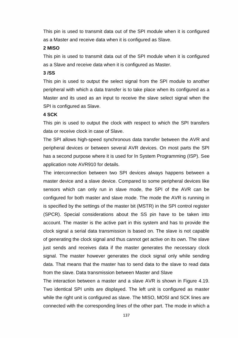
137
This pin is used to transmit data out of the SPI module when it is configured
as a Master and receive data when it is configured as Slave.
2 MISO
This pin is used to transmit data out of the SPI module when it is configured
as a Slave and receive data when it is configured as Master.
3 /SS
This pin is used to output the select signal from the SPI module to another
peripheral with which a data transfer is to take place when its configured as a
Master and its used as an input to receive the slave select signal when the
SPI is configured as Slave.
4 SCK
This pin is used to output the clock with respect to which the SPI transfers
data or receive clock in case of Slave.
The SPI allows high-speed synchronous data transfer between the AVR and
peripheral devices or between several AVR devices. On most parts the SPI
has a second purpose where it is used for In System Programming (ISP). See
application note AVR910 for details.
The interconnection between two SPI devices always happens between a
master device and a slave device. Compared to some peripheral devices like
sensors which can only run in slave mode, the SPI of the AVR can be
configured for both master and slave mode. The mode the AVR is running in
is specified by the settings of the master bit (MSTR) in the SPI control register
(SPCR). Special considerations about the SS pin have to be taken into
account. The master is the active part in this system and has to provide the
clock signal a serial data transmission is based on. The slave is not capable
of generating the clock signal and thus cannot get active on its own. The slave
just sends and receives data if the master generates the necessary clock
signal. The master however generates the clock signal only while sending
data. That means that the master has to send data to the slave to read data
from the slave. Data transmission between Master and Slave
The interaction between a master and a slave AVR is shown in Figure 4.19.
Two identical SPI units are displayed. The left unit is configured as master
while the right unit is configured as slave. The MISO, MOSI and SCK lines are
connected with the corresponding lines of the other part. The mode in which a
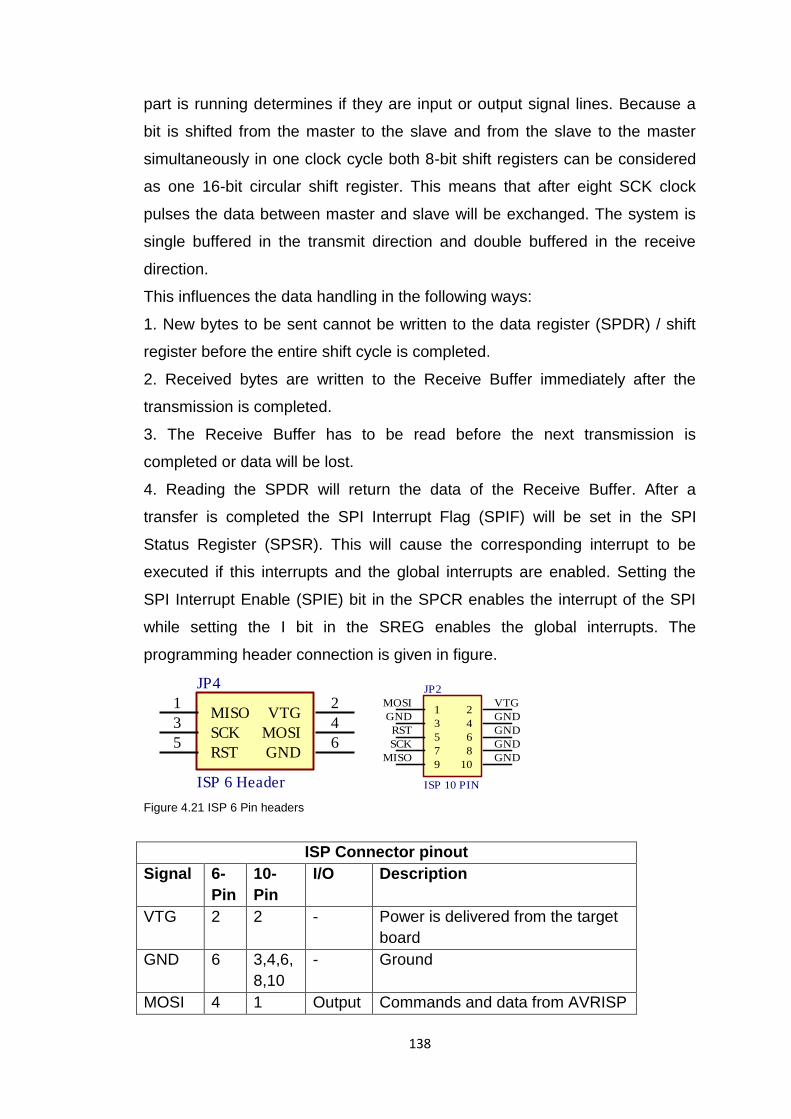
138
part is running determines if they are input or output signal lines. Because a
bit is shifted from the master to the slave and from the slave to the master
simultaneously in one clock cycle both 8-bit shift registers can be considered
as one 16-bit circular shift register. This means that after eight SCK clock
pulses the data between master and slave will be exchanged. The system is
single buffered in the transmit direction and double buffered in the receive
direction.
This influences the data handling in the following ways:
1. New bytes to be sent cannot be written to the data register (SPDR) / shift
register before the entire shift cycle is completed.
2. Received bytes are written to the Receive Buffer immediately after the
transmission is completed.
3. The Receive Buffer has to be read before the next transmission is
completed or data will be lost.
4. Reading the SPDR will return the data of the Receive Buffer. After a
transfer is completed the SPI Interrupt Flag (SPIF) will be set in the SPI
Status Register (SPSR). This will cause the corresponding interrupt to be
executed if this interrupts and the global interrupts are enabled. Setting the
SPI Interrupt Enable (SPIE) bit in the SPCR enables the interrupt of the SPI
while setting the I bit in the SREG enables the global interrupts. The
programming header connection is given in figure.
Figure 4.21 ISP 6 Pin headers
ISP Connector pinout
Signal 6-
Pin
10-
Pin
I/O Description
VTG 2 2 - Power is delivered from the target
board
GND 6 3,4,6,
8,10
- Ground
MOSI 4 1 Output Commands and data from AVRISP
MISO1
VTG2
SCK3
MOSI4
RST5
GND6
JP4
ISP 6 Header
1MOSI
2VTG
3GND
4GND
5RST
6GND
7SCK
8GND
9MISO
10GND
JP2
ISP 10 PIN

139
to target AVR
MISO 1 9 Input Data from target AVR to AVRISP
SCK 3 7 Output Serial Clock, Controlled by
AVRISP
RESET 5 5 Output Reset. Controlled by AVRISP
Table 4.10 ISP Signals
More on SPI interface and its block diagram will be found on the datasheet of
ATmega128 or ATmega16L.