theoretical efficiency of multiplier devices · theoretical efficiency of multiplier devices ......
TRANSCRIPT
Second International Symposium on Space Terahertz Technology Page 197
THEORETICAL EFFICIENCY OF MULTIPLIER DEVICES
Timo J. Tolmunen and Margaret A. FrerkingJet Propulsion Laboratory
California Institute of Technology
Pasadena, California 91109, U.S.A.
Abstract
During the past few years, several new devices have been proposed for use in frequencymultipliers at millimeter and submillimeter wavelengths. Candidate diodes include a
quantum well diode, a single barrier varactor, a barrier-intrinsic-N diode, a delta-dopedvaractor and a high electron mobility varactor. In comparison to the conventional Schottkyvaractor, these new diodes have some potential advantages in their characteristics, such as astronger nonlinearity or a special-symmetry, which make them very attractive for millimeterand submillimeter wave frequency multiplication. This paper gives an overview of thesenovel devices and their potential benefits in comparison to the conventional Schottky-barriervaractor. Their performance has been analyzed theoretically in various low and high order
multipliers for 200 GHz and 1 THz.
Introduction
Basic scientific research including radio astronomy, remote sensing of the atmosphere,plasma diagnostics and laboratory spectroscopy has long been the primary application forshorter millimeter and submillimeter wave technology. More recently this spectral rangeis also being considered for space-borne radar and communication systems. Fundamentallocal oscillator sources available today for low-noise heterodyne receiver systems includetube oscillators, gas lasers and solid-state sources. The tube oscillators and lasers can coverfrequencies well above 1. THz, but especially for space-borne applications, these sources

Page 198 Second International Symposium on Space Terahertz Technology
require considerable improvement to reduce size or to increase lifetime and reliability. Solid-state sources such as Gunn oscillators do not have these disadvantages, but operate only upto about 200 GHz. Therefore, frequency multipliers are needed to achieve higher frequencies.
The standard "workhorse", the GaAs Schottky-barrier varactor multiplier, is exten-sively used for signal generation at millimeter and submillimeter wavelengths. Althoughthere are still some incomplete areas in the study and optimization of this diode, such as thebehaviour of the CV characteristics close to the built-in potential or the effect of multipliercooling, the Schottky varactor has shown to be an efficient device, both theoretically andexperimentally [1,2] at millimeter and lower submillimeter wavelengths. However, consider-able improvement is still required at frequencies over 500 GHz in order to fulfill input powerrequirements of mixer devices.
While standard Schottky varactor technology is still maturing, several novel diodeshave been proposed for use as multipliers at millimeter and submillimeter wavelengths.These diodes include a quantum well diode [3], a single barrier varactor {4}, a BIN diode(barrier-intrinsic-a+ ) {5}, a delta-doped varactor [6] and a high electron mobility varactor
[7]-
In comparison to the Schottky varactor, these new diodes have some potential advan-tages in their characteristics, such as a stronger nonlinearity or a special-symmetry, whichmake them very attractive for millimeter and submillimeter wave frequency multiplication.Stronger nonlinearities allow more efficient harmonic generation with smaller input signallevels, and more efficient higher-order harmonic generation with unoptimized idler termina-tions.
By using a device having a symmetric C-V curve or an antisymmetric I-V curve, onlyodd-harmonics are generated. Therefore, there is no need for an idler termination in the caseof a frequency tripler. Similarly a frequency quintupler requires only one idler terminationat the 3rd harmonic for optimum operation. Schottky varactors, or other devices, havingasymmetric curves generally require an idler termination at each intermediate harmonicfrequency.
This paper gives a brief overview of these novel diodes and their theoretical performanceas multipliers at millimeter and submillimeter wavelengths. All of these diodes areconsiderably less mature than the conventional Schottky varactor. Therefore, there shouldbe opportunity for device optimization for each application.
c=1 + 02€/qNdw2)iVii'
asCO
(1)
Second International Symposium on Space Terahertz Technology Page 199
Devices
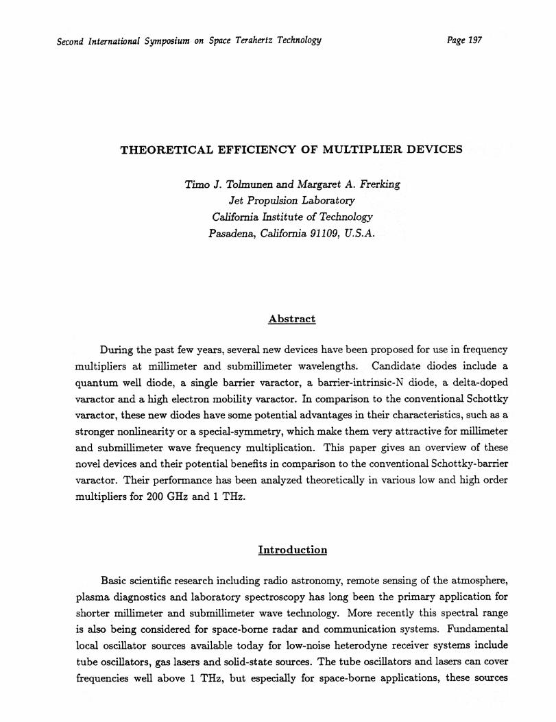
The quantum well diode (QWD) has been the subject of theoretical and experimentalstudies since 1970 [8]. Its high speed [9] and the negative differential resistance make itattractive for millimeter-wave oscillators and its highly nonlinear antisymmetric .r-V curve issuitable for frequency multiplication. The quantum well diode has a thin (20-60 A) undopedlayer (well) sandwiched between two thin barriers (10-50 A) of material having a largerband-gap than the well (Fig. la). This structure acts as a resonator which exhibits peaksin electron transmission (current) at certain values of incident electron energy (voltage).Therefore, the QWD has regions of negative differential resistance when the voltage is justgreater than the resonance.
In addition to a voltage-dependent resistance (Fig. 1b), the quantum well diode has ahighly nonlinear capacitance related to the epitaxial layers exterior to the barriers. Under theassumption that no current flows through the device, the capacitance can be approximated
where Co is the zero-bias capacitance, which depends on the diode area A and the totalthickness of the double barrier structure w (w = 2wbarrier wweti), € is the dielectricconstant, q is the electron charge, Nd is the doping concentration outside the barriers andvi is the junction voltage. If the epitazdal layer width and doping concentration is equalin both sides of the double barrier structure, the C-V curve is symmetric and can generateonly odd harmonics without external biasing. Quantum well diodes have been demonstratedas a tripler to 200 GHz [10]. The tripling mechanism has since been determined to bethe nonlinear C-V characteristic rather than the 1 .-V characteristic. Recent capacitance
measurements of the quantum-well diodes have revealed that the C-V curve is less nonlinearat small voltages and exhibits an extra peak in the capacitance at voltages close to thenegative differential resistance (Fig. 1c) [11].
Theoretically the resistive multiplication is far less efficient than the reactive and itoften merely decreases the device performance as a multiplier. Therefore, it is reasonableto suppress the effects of the nonlinear resistance, if this is possible. The structure of thequantum well diode can be modified by replacing the well and dual barriers with a singlebarrier which is thick enough (150-200 A) for suppressing the current flow through thedevice. The resulting diode, a single barrier varactor (SBV) [4], has a theoretical capacitancewhich is symmetric and follows Eq. (1) (Fig. 1c). This makes the SBV (also called quantum
Depletion Region
Well
Depletion Region
InGaAs
InAlAsInGaAsInAlAs
InGaAs
GaAs/AlAs15-45-15 A4—um—diam
InGaAs/AlAs23-47-23 A3—um—diam
Page 200 Second International Symposium on Space Terahertz Technology
—2 —1 0 1 2DIODE VOLTAGE [V]
-2 -1.5 -1 -0.5 0 0.5 1 1.5 2-2.5 4.5 -1 -0.5 0 0.5 1 1.5 2VOLTAGE (V) VOLTAGE (V)
Figure 1. a) Structure of the quantum well diode. In a single barrier varactor only one barrier isused between epitaxial layers. This barrier is made thick enough in order to suppress the current flowthrough the device. b) Examples of measured I-V curves of quantum well diodes. c) Theoreticaland experimental C-V curve of a quantum well (left) and a single barrier varactor diode (right).The theoretical curve of the quantum well diode is based on a more detailed model which takes intoaccount current flow through the device.
Second International Symposium on Space Terahertz Technology Page 201
barrier varactor, QBV) very attractive in millimeter wave multiplier applications.
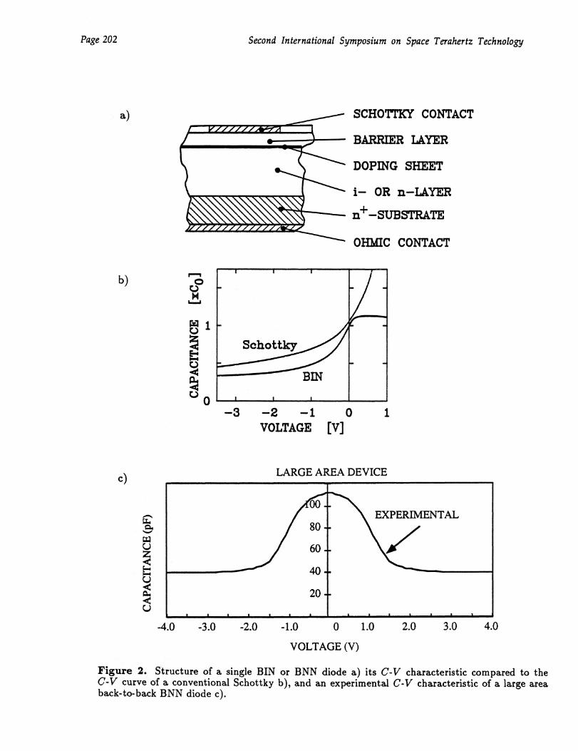
The Barrier-Intrinsic-N (BIN) diode has been proposed as an improved varactor diodefor harmonic multiplication [5]. Unlike quantum well diodes or single barrier varactors whichconsist of a heterostructure and two ohmic contacts as terminals, the BIN diode is essentiallya Schottky varactor with an unique doping profile that yields a sharper C-V characteristic.The diode consists of a Schottky-contact, a barrier layer (thickness d i ), a sheet doping layerand an intrinsic layer (thickness d 2 ) on a highly doped substrate (Fig. 2a). Generally, thediode may be designed so that at zero or low reverse bias, the sheet doping layer is justbarely depleted and the capacitance is
eACmax - • (2)
di
As the reverse voltage increases the depletion region switches to d i + d2 . Because furtherincrease of the bias has no effect on the capacitance due to the high doping of the substrate,the minimum capacitance can be expressed as
Cmin d1 e+Ad2 (3)
Therefore, a single BIN diode has an asymmetric C-V curve (Fig. 2b) which is sharperthan that of the Schottky varactor. By contacting two diodes back-to-back, a symmetric"pulse"-like curve results (Fig. 2c). More importantly, the back-to-back BIN is an inherentlyplanar device having both terminal contacts on the same surface. This is an advantageousfeature, especially for space-borne applications.
Due to the intrinsic layer, the series resistance of the BIN diode is relatively high, whichresults in a low cut-off frequency. In a modification of the BIN diode, the EiNN (barrier-n-n+ ) or delta-doped varactor structure [6,14 a moderately-doped layer is used instead ofthe intrinsic layer to decrease the resistance in the undepleted epita.xial layer.
A high electron mobility varactor is another inherently planar diode which incorporatesthe proven performance of a standard Schottky varactor technology with the electron prop-erties of the two-dimensional electron gas formed, e.g in a GaAs/AlGaAs heterostructure. Inthese structures the electrons have higher mobility than in conventional varactors, especiallyif the device is cooled [7]. The high electron mobility varactor consists of a Schottky-contactfollowed by a two-dimensional electron gas (2-DEG) modulation region (Fig. 3). By apply-
ing a reverse bias to the anode contact, the 2-DEG in the modulation region will becomedepleted near the Schottky-contact, reducing contact capacitance. As the bias is furtherincreased, more of the layer will be depleted. The geometry of the structure results in asheet-like variable capacitor which has an inversely logarithmic dependence on voltage.
ANIII 111 re At/ArAll -4,0%
0
674 1
E-1
C.)'44
C.)
r••■■■
EXPERIMENTAL00 —
80 —
60 —
40 —
20 —
Page 202 Second International Symposium on Space Terahertz Technology
SCHOTTKY CONTACT
BARRIER LAYER
DOPING SHEET
- OR n-LAYER
n+-SUBSTRATE1:44/12FAIrdirArArArAPFAVAIr A-211•41V
OHMIC CONTACT
17:1
04
-3 -2 -1 0 1VOLTAGE [11]
LARGE AREA DEVICE
-3.0 -2.0 -1.0 0 1.0 2.0 3.0 4.0
VOLTAGE (V)
Figure 2. Structure of a single BIN or BNN diode a) its C-V characteristic compared to theC-V curve of a conventional Schottky b), and an experimental C-V characteristic of a large areaback-to-back BNN diode c).

a)
10
Second International Symposium on Space Terahertz Technology Page 203
—20 —10BIAS VOLTAGE [V]
Figure 3. Structure of the high electron mobility varactor a) and its C-V characteristic b).
The equivalent circuit of each diode described above is similar to that of the Schottkyvaractor. It consists of a parallel combination of a voltage-dependent capacitance andconductance, in series with a frequency (and voltage) dependent resistance. For the presentwork the simulations were carried out using this diode model and a modified version of the
large signal analysis program by Siegel and Kerr [13].
Multipliers for 200 GHz
For diodes having an asymmetric C-V curve, the basic multiplier configuration is a
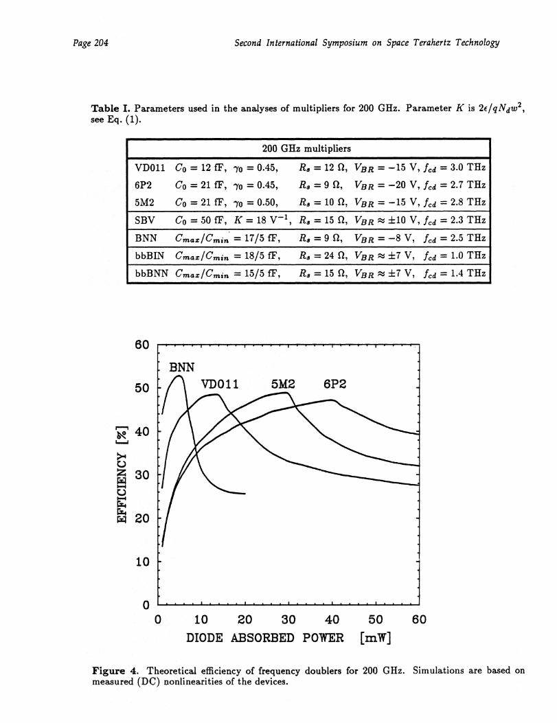
doubler. Fig. 4 illustrates the theoretical efficiency of a delta-doped varactor or BNN andthree Schottky varactor (6P2 and 5M2 by University of Virginia and VD011 by FarranTechnology) doublers for 200 GHz. Although the nominal diode parameters (Table I) arerather different, the dynamic cut-off frequency is almost equal, which results in the samepeak-efficiency. This peak is reached with a voltage swing from near forward conduction
10
I
50
Page 204 Second International Symposium on Space Terahertz Technology
Table I. Parameters used in the analyses of multipliers for 200 GHz. Parameter K is 2€1qNdw2,see Eq. (1).
200 Gliz multipliers
VD011 Co = 12 IF, 'yo = 0.45 Rs = 12 1/, VBR = —15 V, fa = 3.0 THz
6P2 Co = 21 IF, -yo = 0.45 Rs = 9 Si, VBR = —20 V, .f.cd = 2.7 Tflz
5M2 Co = 21 IF, -yo = 0.50 118 = 10 n, VBR = —15 V, icd = 2.8 THz
SBV Co = 50 if, K = 18 V-1 , Rs = 15 n, VBR P4 ±10 V, fcd = 2.3 THz
BNN Cmaz/Cmin * = 17/5 if', Rs = 9 S/, VBR = — 8 V, efcci = 2.5 THz
bbBIN Cmax/Cmin = 18/5 if, Rs = 24 12, VBR'',.= ±7 V, icd = 1.0 THz
bbBNN Cmax/Cmin = 15/5 if, R. = 15 12, VBR ,'kd, ±7 V, icd = 1.4 THz
60
BNN
10 20 30 40 50 60
DIODE ABSORBED POWER [mW]
Figure 4. Theoretical efficiency of frequency doublers for 200 GHz. Simulations are based onmeasured (DC) nonlinearities of the devices.
60 —
SBV7 BNN 15V
10 V6 V 6P2
50
10
Second International Symposium on Space Terahertz Technology Page 205
to the break-down. These diodes can handle more input power, but due to the forwardconduction, multiplication then becomes partly resistive which results in a decrease inefficiency. For diode absorbed power, below the peak, the efficiency is determined by thestrength of the non-linearity. Hence, the BNN or delta-doped varactor results in excellentperformance if the input power level is relatively low.
In general the input power level for peak efficiency is a function of the zero-bias
capacitance of a diode. For example, a Schottky varactor having a small area and hencea small Co is favorable for applications where input power is limited. Small capacitanceresults in high input impedance and hence larger voltage swing across the diode for a giveninput power. Therefore, the break-down voltage limit is reached with rather small inputpower levels. When higher input power levels are available, a larger capacitance is a betterchoice, especially if the nonlinearity is sharper (5M2) or break-down limit is higher (6P2).
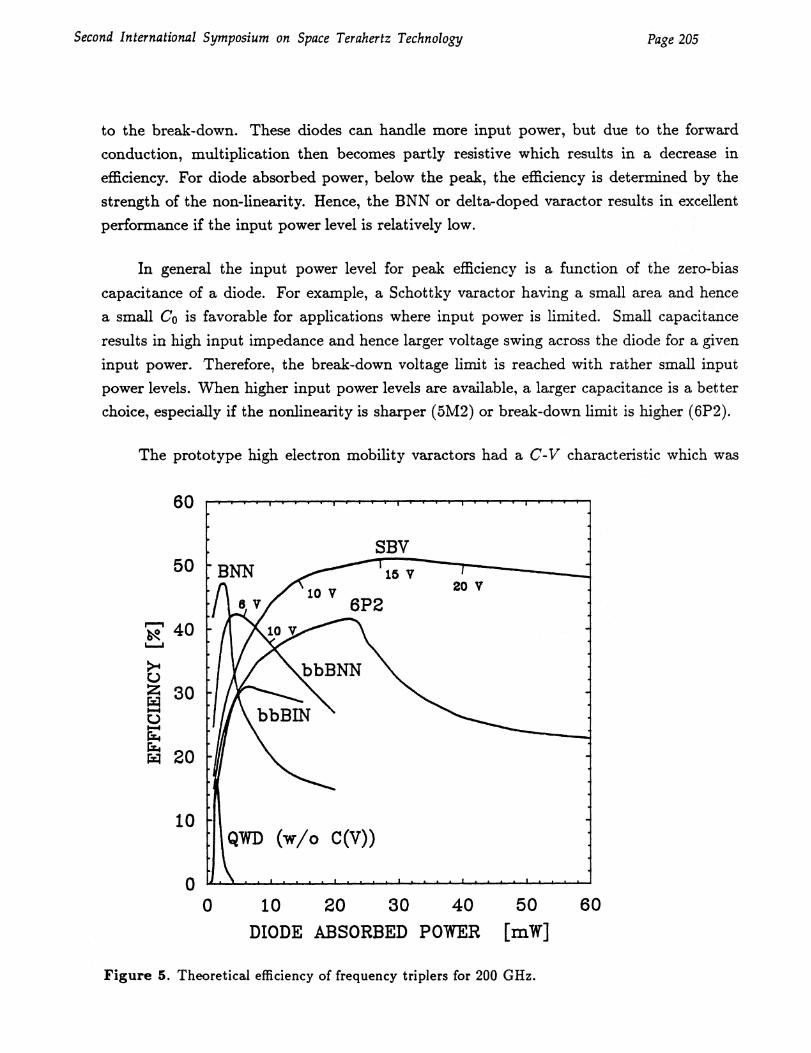
The prototype high electron mobility varactors had a C-V characteristic which was
0 10 20 30 40 50 60
DIODE ABSORBED POWER [mW]
Figure 5. Theoretical efficiency of frequency triplers for 200 GIlz.
Page 206 Second International Symposium on Space Terahertz Technology
sli'ghtly less nonlinear than that of the conventional Schottky varactor [7]. This was partlydue to rather large parasitic capacitance related to the structure. However, it is expected
that a reduction of this parasitic capacitance will result in a curve which is as steep as thatof the conventional Schottky [14]. This together with a measured high break-down voltage[7] make this device very attractive especially for applications, where the input power level
is high.
Comparison of triplers to 200 GHz is shown in Fig. 5. Below the peak, where themultiplication is purely reactive, the theoretical tripling efficiency of the 6P2 and the BNNor delta-doped varactor is close to their doubling efficiency. This is because the input
impedance of a tripler for 200 GHz is higher than the impedance of a doubler for the sameoutput frequency, causing more efficient capacitance modulation. This partly "compensates"additional losses in the diode series resistance at the idler frequency. However, because agood idler termination is crucial for the operation of both devices, degradation of efficiencywill be more severe in practice, due to the difficulty of arranging separate tuning for each
harmonic.
The need for an idler can be avoided using a device having a symmetric C-V curve,such as a single barrier varactor (SBV) or back-to-back BNN (bbBNN). If there is no currentleakage through the single barrier varactor, its highly nonlinear C-V curve together with ahigh dynamic cut-off frequency, results in an excellent 3rd harmonic generation without theneed of an idler. As a hypothetical extreme, a similar size ( 4-pm-diam.) quantum welldiode (Q\VD) was analyzed assuming that multiplication is purely resistive (Experimentally,
the voltage variable capacitance dominates the multiplication). The dramatic difference
between resistive and reactive multiplication can be seen in Fig. 5. Despite the highly
nonlinear I-V curve of the quantum well diode, its theoretical performance for varistor
operation is much less than the varactor's performance.
The back-to-back BIN (bbBIN), also has a sharp symmetric C-V curve, but its ratherlow dynamic cut-off frequency decreases the conversion efficiency. A doped version, a back-to-back BNN, has a lower series resistance and therefore higher cut-off frequency. This resultsin better performance at moderate pump power. Doping in the epitaxial layer degrades thesharpness of the C-V curve so that the efficiency at low pump power is reduced.
Experimentally, the efficiencies available from multipliers will be lower due to resistive
losses, which in the 200-Gliz range in a well-made waveguide mount are typically around
1.5-2 dB, with an additional 0.5-1 dB for each idler frequency. The efficiency will furtherdecrease due to the difficulty to provide the device with optimum terminations at eachharmonic frequency. For the best performance, the diode should be matched at the input

20
Second International Symposium on Space Terahertz Technology Page 207
Table II. Parameters used in the analysis of the multipliers for 1000 Gliz.
1 THz multipliers
2T2 Co = 5.5 fF, Pyo = 0.45, Rs = 12 n VBR= —10 V, .fcd = 5.8 THz
SBV Co = 15 fF, K = 18 V- 1 , Rs = 20 S/ VBR;•`1, ±10 V, icd = 5.0 Tliz
QWD(C) Co = 50 fF, K = 112 V-1 , R, = 20 n VBR .,:i ±3 V
BNN Cmax/Cmin = 4.5/1.2 if, R, = 17 S/ VBR= — 8 V, icd = 5.7 Tllz
bbBIN Cmax/Cmin = 7.5/2.1 if, Rs = 40 a VBR 'At% ±5 V, fcd = 1.4 Tliz
, bbBNN Cmax/Cmin = 5.6/2.0 IF, li, = 20 n, VBR",,s ±5 V, icd = 2.6 Tllz ,
and output frequency, and terminated at the idler(s) with an inductance which resonates
with the average capacitance at that particular frequency. At harmonic frequencies higherthan the output an optimum termination is an open circuit, because other terminations
5 10 15 20DIODE ABSORBED POWER [In-W]
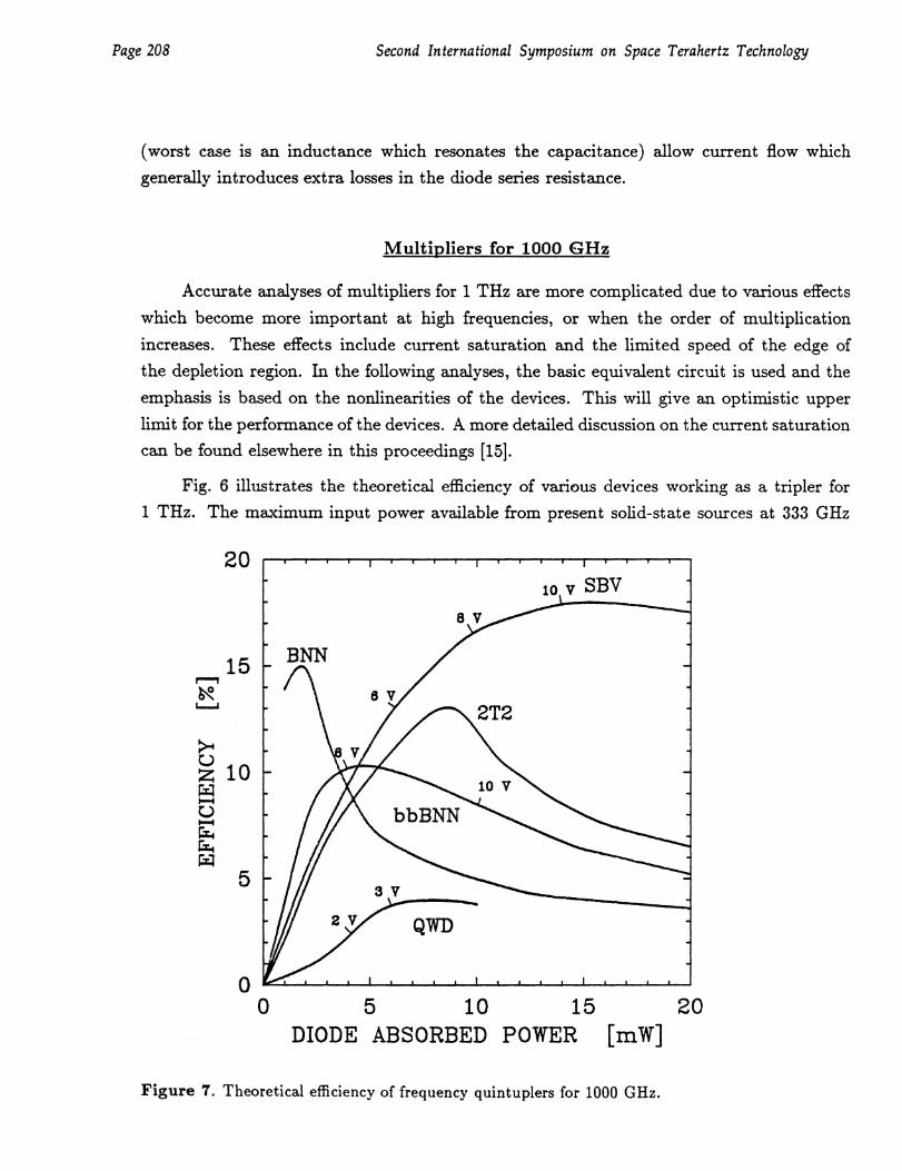
Figure 6. Theoretical efficiency of frequency triplers for 1000 Gllz.
Page 208 Second International Symposium on Space Terahertz Technology
(worst case is an inductance which resonates the capacitance) allow current flow whichgenerally introduces extra losses in the diode series resistance.
Multipliers for 1000 GHz
Accurate analyses of multipliers for 1 THz are more complicated due to various effects
which become more important at high frequencies, or when the order of multiplicationincreases. These effects include current saturation and the limited speed of the edge ofthe depletion region. In the following analyses, the basic equivalent circuit is used and the
emphasis is based on the nonlinearities of the devices. This will give an optimistic upperlimit for the performance of the devices. A more detailed discussion on the current saturationcan be found elsewhere in this proceedings [15].
Fig. 6 illustrates the theoretical efficiency of various devices working as a tripler for1 THz. The maximum input power available from present solid-state sources at 333 GHz
20
0 5 10 15 20DIODE ABSORBED POWER [rnW]
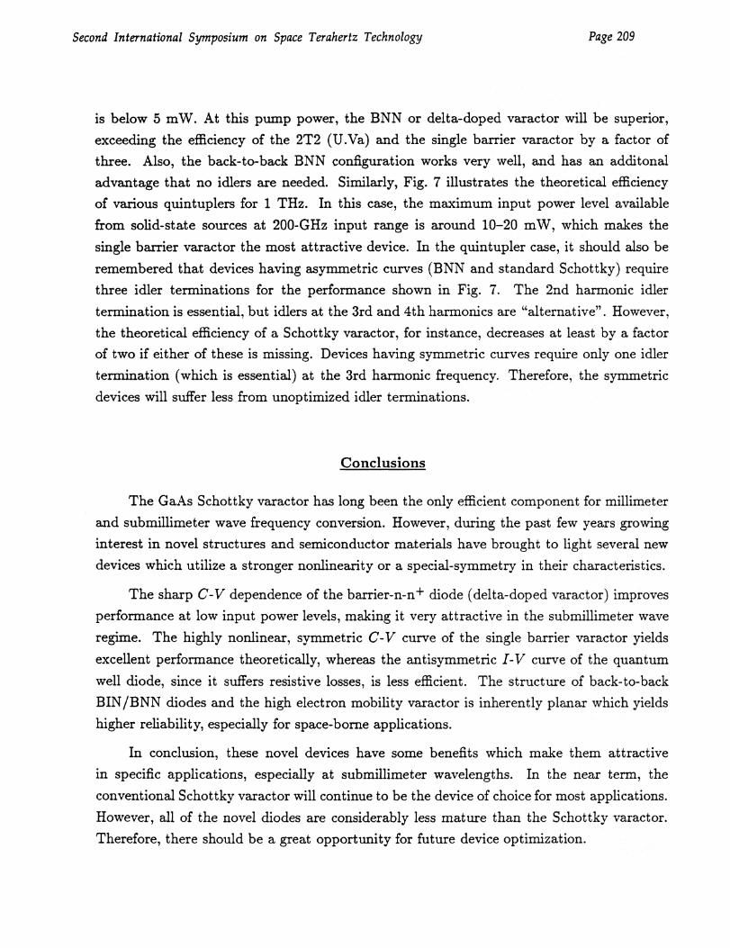
Figure 7. Theoretical efficiency of frequency quintuplers for 1000 Gllz.
Second International Symposium on Space Terahertz Technology Page 209
is below 5 mW. At this pump power, the BNN or delta-doped varactor will be superior,exceeding the efficiency of the 2T2 (U.Va) and the single barrier varactor by a factor ofthree. Also, the back-to-back BNN configuration works very well, and has an additonaladvantage that no idlers are needed. Similarly, Fig. 7 illustrates the theoretical efficiencyof various quintuplers for 1 THz. In this case, the maximum input power level available
from solid-state sources at 200-GHz input range is around 10-20 mW, which makes the
single barrier varactor the most attractive device. In the quintupler case, it should also beremembered that devices having asymmetric curves (BNN and standard Schottky) requirethree idler terminations for the performance shown in Fig. 7. The 2nd harinonic idlertermination is essential, but idlers at the 3rd and 4th harmonics are "alternative". However,the theoretical efficiency of a Schottky varactor, for instance, decreases at least by a factorof two if either of these is missing. Devices having symmetric curves require only one idlertermination (which is essential) at the 3rd harmonic frequency. Therefore, the symmetricdevices will suffer less from unoptimized idler terminations.
Conclusions
The GaAs Schottky varactor has long been the only efficient component for millimeterand submillimeter wave frequency conversion. However, during the past few years growinginterest in novel structures and semiconductor materials have brought to light several newdevices which utilize a stronger nonlinearity or a special-symmetry in their characteristics.
The sharp C-V dependence of the barrier-n-n+ diode (delta-doped varactor) improvesperformance at low input power levels, making it very attractive in the submillimeter wave
regime. The highly nonlinear, symmetric C-V curve of the single barrier varactor yields
excellent performance theoretically, whereas the antisymmetric I-V curve of the quantum
well diode, since it suffers resistive losses, is less efficient. The structure of back-to-backBIN/BNN diodes and the high electron mobility varactor is inherently planar which yieldshigher reliability, especially for space-borne applications.
In conclusion, these novel devices have some benefits which make them attractivein specific applications, especially at submillimeter wavelengths. In the near term, theconventional Schottky varactor will continue to be the device of choice for most applications.However, all of the novel diodes are considerably less mature than the Schottky varactor.Therefore, there should be a great opportunity for future device optimization.
Page 210 Second International Symposium on Space Terahertz Technology
Acknowledgements
The research described in this paper was performed by the Center for SpaceMicroelectronics, Jet Propulsion Laboratory, California Institute of Technology and wassponsored by the National Aeronautics and Space Administration, Office of Aeronautics,
Exploration, and Technology. The authors wish to thank P. Batelaan, T. Crowe, E. Kollberg,
U. Lieneweg, .1. Maserjian, B. Peatman, D. Rutledge and P. Siegel for valuable discussions.
References
[1] N. Erickson, "High effieciency submillimeter frequency multipliers." 1990 IEEE
MTT-S International Microwave Symposium Digest, 1301-1304, 1990.
{2) T. Tolmunen, "High-efficiency Schottky-varactor frequency multipliers at millimeterwaves." Helsinki University of Technology, Radio Laboratory, Report 5180, 1989. (Partlypublished in Int. J. of Infrarecl and Millimeter Waves, Vol. 8, 1987, pp. 1313-1353 and Vol.10, 1989 pp. 475-518.)
{3} T.C.L.G. Sollner, W.D. Goodhue, P.E. Tannenwald, C.D. Parker and D.D. Peck,"Resonant tunneling through quantum wells at frequencies up to 2.5 THz." App/. Phys.Lett., Vol. 43, 588-590, (1983).
[4] E. Kollberg, A. Rydberg, "Quantum-barrier-varactor diodes for high-efficiencymillimeter wave multipliers,"Electron. Lett., Vol. 25, No. 25, 1696-1697, (1989).
{5} U. Lieneweg, B.R. Hancock, J. Maserjian, "Barrier-Intrinsic-N + (BIN) diodes fornear-millimeter wave generation", Conference Digest for the Twelft International Conferenceon Infrared and Millimeter Waves, 6-7, 1987.
[6] B.J. Rizzi, T.W. Crowe, and W.C.B. Peatman, "A 8-doped varactor diode forsubmillimeter wavelengths", Conference digest for the 15th International Conference onInfrared and Millimeter Waves, SPIE Cat. No. 90-50878, pp 478-480, 1990.
[7]W.C.B. Peatman and T.W. Crowe, "A high electron mobility varactor." Conferencedigest for the 15th International Conference on Infrared and Millimeter Waves, SPIE Cat.No. 90-50878, pp 473-474, 1990.
[8] L. Esaki and R. Tsu, "Superlattice and negative differential conductivity insemiconductors,"IBM J. Res. Develop., Vol. 24, 61-65, (1970).
[9] E.R. Brown T.C.L.G. Saner, C.D. Parker, W.D. Goodhue and C.L. Chen,
Second International Symposium on Space Terahertz Technology Page 211
"Oscillations up to 420 GHz in GaAs/AlAs resonant tunneling diodes," Appl. Phys. Lett.,
Vol. 55, 1777-1779, (1989).
[10]P.D. Batelaan and M.A. Frerking, "Quantum well multipliers," Conference Digestfor the Twelfth International Conference on Infrared and Millimeter Waves 14-15, 1987.
[11] O. Bork, T.J. Tolmunen, M.A. Frerking, 3.13. Hacker and D.B. Rutledge,
"S parameter measurements of quantum well diodes." Conference digest for the 15th
International Conference on Infrared and Millimeter Waves SPIE Cat. No 90-50878,pp. 251-253, 1990.
[12]U. Lieneweg, T. Tolmunen, M. Frerking and J. Maserjian," Design of planar var-actor frequency multiplier devices with blocking barriers," Second International Symposiumon Space Terahertz Technology, this proceedings.
[13]P.11. Siegel, A.R. Kerr and W. Hwang, "Topics in the optimization of millimeter-wave mixers," NASA Technical Paper 2287, 512 p., 1984.
[14]Private discussions with B. Peatman, U.Va.
{15] E. Kollberg, T. Tolmunen, M. Frerking, 3. East, "Current Saturation in
Submillimeter Wave Varactors," Second International Symposium on Space TerahertzTechnology, this proceedings.