theoretical investigation of gain-clamped semiconductor optical amplifiers using the amplified...
TRANSCRIPT

1DtecawgsiitSpali(tg
fppocs(o(popc
Xin-Hong Jia Vol. 23, No. 12 /December 2006 /J. Opt. Soc. Am. B 2503
Theoretical investigation of gain-clampedsemiconductor optical amplifiers
using the amplified spontaneous emissioncompensating effect
Xin-Hong Jia
School of Physics, Sichuan Normal University, Chengdu 610068, China
Received April 19, 2006; revised September 3, 2006; accepted September 3, 2006; posted September 8, 2006 (Doc. ID 70055)
The theoretical model on gain-clamped semiconductor optical amplifiers (GC-SOAs) based on compensatinglight has been constructed. Using this model, the effects of insertion position and peak reflectivity of the fiberBragg grating (FBG) on the gain clamping and noise figure (NF) characteristics of GC-SOA are analyzed. Theresults show that the effect of the FBG insertion position on gain clamping is slight, but the lower NF can beobtained for input FBG-type GC-SOA; when the FBG peak wavelength is designed to close the signal wave-length, the gain clamping and NF characteristics that can be reached are better. Further study shows that,with the increased peak reflectivity of the FBG, the critical input power is broadened and the gain tends to bevaried slowly; the larger bias current is helpful to raise gain and decrease the noise figure but is harmful to again flatness characteristic. © 2006 Optical Society of America
OCIS codes: 250.5980, 050.2770.
rsgsctlcrcbltTb
2TSul
Sat
wN
. INTRODUCTIONue to the properties of broadband—high gain, better in-
egration, lower cost, etc.—semiconductor optical amplifi-rs (SOAs) have considerable potential for use in opticalommunication systems such as being used as in-linemplifiers1–5 and high-speed optical switches.6,7 In denseavelength-division-multiplexing (DWDM) networks, theain saturation of the conventional SOAs would lead toerious interchannel cross talk and signal distortion ands regarded as the main limit factor to further expand thenput dynamic range and system capability.6,8 In contrast,he gain-clamped semiconductor optical amplifier (GC-OA) is paid special attention to because of the higher in-ut saturation power.9–16 In the GC-SOA, carrier densitynd optical gain are stabilized by introducing lasing oscil-ation near the signal wavelength. Often, the gain clamp-ng can be realized by the distributed Bragg reflectorDBR) attached to the ends of the active section9–12 or byhe distributed feedback (DFB) structure inside the wave-uide layer.13,14
However, the channel transmission rate is restrictedrom the relaxation oscillation (RO).9,10 In fact, this im-act also occurs in gain-clamped erbium-doped fiber am-litude (EDFA) (GC-EDFA) based on the lasing effect. Tovercome this disadvantage, a kind of novel gain-lamping scheme based on compensating light isuggested.17,18 In this configuration, a fiber Bragg gratingFBG) is inserted near an end of the conventional EDFAr SOA to reflect the amplified spontaneous emissionASE), and the gain clamping can be achieved by the com-ensating effect between the signal and the ASE. Basedn the previous work, this paper has constructed a com-rehensive theoretical model of the GC-SOA based on theompensating effect by using the traveling-wave and car-
0740-3224/06/122503-8/$15.00 © 2
ier rate equations, and the systematic numerical analy-is on the influence of device parameters on the GC-SOAain and noise figure (NF), is also performed. The resultshow that the effect of the FBG insertion position on gainlamping is slight but the lower NF can be obtained forhe input FBG-type GC-SOA; when the FBG peak wave-ength is designed to close the signal wavelength, the gainlamping and noise figure characteristics that can beeached are better. Further study shows that, with the in-reased FBG peak reflectivity, the critical input power isroadened and the gain tends to be varied slowly; thearger bias current is helpful to raise gain and decreasehe NF but is harmful to a gain flatness characteristic.hese results may provide an instructive insight and areeneficial for the device design and optimization.
. THEORETICAL MODELhe schematics of the input and output FBG-type GC-OAs are shown in Fig. 1, where the optical isolator issed to ensure the single-direction traveling for the signal
ight.The signal optical field inside the active layer of the
OA can be expressed by the sum of forward wave Asigf
nd backward wave Asigb , which obey the following
raveling-wave equations,19
dAsigf
dz= �− i� +
1
2��g��sig,N� − ���Asig
f , �1a�
dAsigb
dz= �i� −
1
2��g��sig,N� − ���Asig
b , �1b�
here � is the confinement factor, � is the loss coefficient,is the carrier density, � and g�� N�, respectively, ac-
sig sig006 Optical Society of America

c�ld
wrt
c
wotwSpo
i
o
wttS
tdgsbcwassP
wRwe
w
g
w
d
waatAd
wlc
dsgs
Fm
2504 J. Opt. Soc. Am. B/Vol. 23, No. 12 /December 2006 Xin-Hong Jia
ount for the signal central frequency and gain coefficient,=2�n�sig/c is the propagation constant, c is the light ve-
ocity in vacuum, and n is the effective mode refractive in-ex, which can be expressed by
n = n0 +dn
dNN, �2�
here n0 is the effective refractive index at the zero car-ier injection, and dn /dN denotes the variation slope ofhe refractive index with respect to the carrier density.
Forward and backward waves satisfy the boundaryonditions as below
z = 0: Asigf �0� = �1 − R1��sig�Asig
i �0� + �R1��sig�Asigb �0�,
�3a�
z = L: Asigb �L� = �R2��sig�Asig
f �L�,
Asigt �L� = �1 − R2��sig�Asig
f �L�, �3b�
here Asigi and Asig
t are the input and transmitted signalptical fields, R1��� and R2��� express the effective reflec-ivities for the front and back facets of the GC-SOA,hich are determined by the facet reflectivities of theOA and the structure parameters of the FBG. For sim-licity, the frequency dependences of them take the formf
nput FBG type:
R1��� = Rmax exp�−�� − �0�2
��2 � + cons tan t,
R2��� = cons tan t, �4a�
utput FBG type:
R1��� = cons tan t,
R2��� = Rmax exp�−�� − �0�2
��2 � + cons tan t, �4b�
here Rmax is the peak reflectivity, �0 is the peak reflec-ion frequency, and �� is used to characterize the reflec-ion bandwidth. In this paper, the facet reflectivity of theOA is taken to be 4.0�10−5.12
ig. 1. (a) Schematic of the input FBG-type GC-SOA. (b) Sche-atic of the output FBG-type GC-SOA.
Although the spontaneous emission noise generated byhe amplifier together with the signal wave takes part inraining the available carriers and helps saturate theain, it is not necessary to treat it as a coherent lightince it distributes itself continuously over a relativelyroad band of wavelengths [�200 nm can be reached ifarrier densities attain up to several �1018 cm−3 (Ref. 3)]ith random phases. The same treatment method canlso be found in Refs. 11 and 19–22. Under this circum-tance, the ASE power spectra can also be written as theum of the forward wave PASE
f ��� and backward wave
ASEb ���, which are found to satisfy20
dPASEf ���
dz= ��g��,N� − ��PASE
f ��� + Rsp��,N�, �5a�
dPASEb ���
dz= − ��g��,N� − ��PASE
b ��� − Rsp��,N�, �5b�
here g�� ,N� the ASE gain coefficient at frequency �,sp�� ,N� is the power spectra of the ASE coupled into theaveguide mode per unit and is related to the stimulatedmission rate Rs�� ,N� as19,23
Rsp��,N� = �Rs��,N�h�, �6�
here h� is the photon energy.The boundary conditions of the ASE power spectra are
iven by
z = 0: PASEf �0,�� = R1���PASE
b �0,��, �7a�
z = L: PASEb �L,�� = R2���PASE
f �L,��,
PASEt �L,�� = �1 − R2����PASE
f �L,��, �7b�
here PASEt �L ,�� is the transmitted ASE power spectra.
Under the steady state, the carrier rate equation can beescribed by24
I
qV = ��N�N�z� +�g��sig,N�Psig�z�
Acrossh�sig
+ 2 �g��,N�PASE�z,��
Acrossh�d�, �8�
here I is the biasing current, q is the electron charge, Vnd Across are the active-layer volume and cross-sectionalrea, Psig= Asig
f 2+ Asigb 2 is the total signal power, the fac-
or 2 originates from the two polarization states of theSE, and ��N� is the nonstimulated recombination rate,efined by24
��N� = A + BN + CN2, �9�
here A ,B ,C are the nonradiative recombination, bimo-ecular radiative recombination, and Auger recombinationoefficients, respectively.
Considering the broadband ASE spectra, the depen-ence of material gain on the frequency and carrier den-ity must be included more precisely. The gain coefficientcan be calculated by the difference of stimulated emis-
ion rate R and stimulated absorption rate R (Ref. 19),
s s
w
wlt
ceffitss
wC
rc
wS
sf
S
LAV�
�
nn
d
TECT
Am
m
m
�
ABC
Xin-Hong Jia Vol. 23, No. 12 /December 2006 /J. Opt. Soc. Am. B 2505
g��,N� = Rs��,N� − Ra��,N�, �10a�
ith
Rs��,N� =c2
4�2�3/2n12�2� 2memhh
�me + mhh��3/2
�Eg/h
� ��� −Eg�N�
hfc�����1 − f������
�� 2T0
1 + �2�T0�2��� − ��2�d��, �10b�
Ra��,N� =c2
4�2�3/2n12�2� 2memhh
�me + mhh��3/2
�Eg/h
� ��� −Eg�N�
hf������1 − fc�����
�� 2T0
1 + �2�T0�2��� − ��2�d��, �10c�
here n1 is the refractive index of the InGaAsP activeayer, = �Arad+BN�−1 is the radiative recombination life-ime, Arad is the linear radiative recombination
Table 1. Device Structure and Mater
ymbol Parame
Active layer
cross Active layer cross-Active layerConfinemen
0 Peak wavelength of the e 3 dB bandwidth of the eq
1 Refractive index of the I
0 Equivalent refractive ininjecti
n /dN Differential of the equivawith respect to the
Active layer te
g0 Bandgap energy witho
BGR Bandgap shrinka
0 Mean lifetime for the coheelectrons with th
rad Linear radiative recom
e Effective mass of the elecband
hh Effective mass of the heavband
lh Effective mass of the lighband
Loss coeffiNonradiative recombi
Bimolecular radiative recAuger recombinat
aReference 12.bReference 18.cReference 20.
oefficient,19 me and mhh are the effective masses of thelectron and heavy hole, T0 represents the mean lifetimeor the coherent interaction of electrons with the opticaleld, fc��� and f���� are the Fermi–Dirac distributions ofhe electron and hole, which can be evaluated by the Nils-on approximation.24 The carrier-dependent bandgaphrinkage is also taken into account24:
Eg�N� = Eg0 − CBGRN1/3, �11�
here Eg0 is the bandgap without carrier injection, andBGR is the bandgap shrinkage coefficient.The NF is a crucial parameter to estimate the deterio-
ation degree of input signal-to-noise ratio (SNR), whichan be defined as
NF =SNRin
SNRout, �12a�
here SNRin and SNRout represent the input and outputNRs, respectively.To calculate NF, we split the SOA length L into M equal
ections from the input end, assume each section is uni-orm, then,12
arameters Used in the Calculations
Value
h 500 �mal area 2�10−13 m2
e 1�10−16 m3
r 0.4489a
ent reflectivity 1551.8 nmnt reflectivity 0.35 nmP active layer 3.5705a
thout carrier 3.2353a
fractive indexr density
−1.3410−26 m−3b
ture 297 Kier injection 0.78 eVc
fficient 9.0�10−11 eV m3b
teraction of theal field
1 psb
n coefficient 1.0�10 s−1b
the conduction 4.1�10−32 kgb
in the valence 4.19�10−3 kgb
in the valence 5.06�10−32 kgb
20 cm−1
coefficient 3.5�108 s−1
tion coefficient 5.6�10−16 m3 s−1
fficient 3.0�10−41 m6 s−1
ial P
ter
lengtsectionvolumt factoquivaluivale
nGaAsdex wionlent recarriemperaut carrge coerent ine opticbinatiotronin
y hole
t hole
cientnationombinaion coe

wttb
wi
assaebsdt(bcrml1a
3TtcflN
AoAFNas=pvnconF�h
btaasAttHFstttFt
Fvw=vw=
2506 J. Opt. Soc. Am. B/Vol. 23, No. 12 /December 2006 Xin-Hong Jia
NF = NF1 +NF2 − 1
G1+
NF3 − 1
G1G2+ ¯ +
NFM − 1
G1G2 ¯ GM−1,
�12b�
here Gj=exp���g�j ,��−��l� �j=1,2, . . . ,M� is the gain ofhe jth subsection, l is the spatial step size, while NFj ishe NF of the jth subsection, which can be expressedy11,12,14
NFj =2nsp�j,���Gj − 1�
Gj+
1
Gj, �12c�
here nsp�j ,�� is the well-known spontaneous emissionnversion factor of the jth subsection, defined as11,12,14
nsp�j,�� =�Rs�j,��
�Rs�j,�� − �Ra�j,�� − �. �12d�
Combining Eqs. (1)–(11), substituting the optical powernd carrier density of each subsection with the corre-ponding averaged values, the self-consistent numericalolution on the longitudinal distribution of optical fieldnd carrier density can be computed by applying the it-ration method. The NF characteristic of the GC-SOA cane analyzed from Eq. (12). In the calculation, the ASEpectrum is sliced into K segments, where the frequency-omain step size is taken to be the integral multiple tohe cavity mode interval,12 thus the integrations in Eqs.8) and (10) can be evaluated by add operations. It shoulde noted that, the precision and validity of this averagingan be improved by increasing M and K. Our simulationesults have shown that if M and K, respectively, approxi-ates to 50 and 200 or more for the conventional SOA
ength (i.e., 500 �m) and the ASE spectrum range (520–1570 nm is selected in this simulation), the carriernd optical field distributions remain unchanged.
. RESULTS AND DISCUSSIONhe device structure and material parameters used inhis simulation are listed in Table 1. In the following dis-ussion, the influences of the insertion position, peak re-ectivity of the FBG, and biasing current on the gain andF of the GC-SOA will be reviewed in detail.
. Influence of the Fiber Bragg Grating Insertion Positionn the Gain-Clamped Semiconductor Opticalmplifier Performanceigures 2(a) and 2(b) show the variations of the gain andF with the input power for the conventional SOA, inputnd output FBG-type GC-SOA, respectively, where theignal wavelength sig=1545 nm, Rmax=0.6, and I100 mA. To be easily understood, the power spectra out-uts of the ASE of the input FBG-type GC-SOA for thearious input powers Pin are also plotted in Fig. 3 (the sig-al light is not included in this figure). From Fig. 2(a), itan be seen that, with the increased input power, the gainf the conventional SOA gradually saturates by accompa-ying the carrier depletion (curve a); after inserting theBG, if the input power is lower than its critical value �−5 dBm�, the SOA gain is clamped at �20 dB, which ex-ibits a better linear amplification characteristic (curves
and c). The features can be explained from Fig. 3: Withhe increased signal input power, the carriers in the SOActive layer are depleted, and the stimulated emissionnd spontaneous emission rates are weakened corre-pondingly. As a consequence, the forward and backwardSE powers tend to be reduced, which makes the carriers
end to be recovered in turn. It is this compensating effecthat stabilizes the total photons and carriers in the SOA.owever, if the input power (0 and 10 dBm are selected inig. 3) exceeds the critical value, the carrier depletion iso strong that the ASE power is decreased drastically,hus the compensating effect between the signal light andhe ASE is weakened significantly, and the gain charac-eristic reveals the same trend with conventional SOA.rom Fig. 2(a), it can also be found that, the difference of
he gain between the input and output FBG-type SOA is
ig. 2. (a) Variations of gain with the input power for the con-entional SOA, input FBG-type, and output FBG-type GC-SOA,here the signal wavelength sig=1545 nm, Rmax=0.6, and I100 mA. (b) Variations of NF with the input power for the con-entional SOA, input FBG-type, and output FBG-type GC-SOA,here the signal wavelength sig=1545 nm, Rmax=0.6, and I100 mA.

saflfa
pGrGowtbiltpiptapi
aog
vcsilaFAaPsrmtqnwbpt
F=
Xin-Hong Jia Vol. 23, No. 12 /December 2006 /J. Opt. Soc. Am. B 2507
light. The answer is that, once other system parametersre fixed, the FBG insertion position only has evident in-uence on carriers and optical field distributions (see the
ollowing discussion), but the averaged carrier densitynd optical field energy have no visible discrepancy.From Fig. 2(b), it can also be seen that if the input
ower is limited within the critical value the NF of theC-SOA decreases with the increased input power (this
elationship is especially evident for the output FBG-typeC-SOA, but is slight for the input FBG-type GC-SOA);nce the critical value is reached, the NF is increasedith the increased input power. This can be attributed to
he fact that the NF of the GC-SOA is mainly determinedy the spontaneous emission inversion factor at the SOAnput end from Eq. (12) (approximates to N / �N−N0�).11 Asong as the input power is under critical value, the varia-ion of the averaged carrier density along the signalropagation direction is smaller, while the optical energys converged to the output end owing to the amplificationrocess. Therefore, the carrier density is concentrated onhe GC-SOA input end with the increased input power,nd the spontaneous emission inversion factor at the in-ut end as well as the NF reveal decreased tendency. Butf the input power is too large, the depletion of the aver-
ig. 3. Power spectra outputs of the ASE of the input FBG-typ10 dBm, (c) P =0 dBm, and (d) P =10 dBm.
in inged carrier density is obvious. As a result, the spontane-us emission inversion factor and NF are enhancedradually.
Figure 2(b) also demonstrates that, similar to the con-entional SOA, when the input power is lower than itsritical value, the NF of the input FBG-type GC-SOA ismaller ��5 dB�, whereas the output FBG-type GC-SOAs opposite (from �8 dB down to �5 dB). For input powerarger than the critical value, the curves in Fig. 2(b) arelmost identical. This phenomenon can be illustrated byig. 4, which depicts the longitudinal distributions of theSE power, signal power, and carrier density for the inputnd output FBG-type GC-SOA, where the input powerin=−20 dBm, other data are the same as in Fig. 2. Ashown in Fig. 4(a), for the input FBG-type GC-SOA, theeflection of the ASE is stronger at the input end, whichakes the forward ASE power at the input end larger
han the backward ASE power at the output end. Conse-uently, after experiencing the similar gain with the sig-al light because of gain clamping [see Fig. 2(a)], the for-ard ASE power at the output end is stronger than theackward ASE power at the input end, i.e., the ASE totalower is mainly concentrated at the output end. In addi-ion, Fig. 4(b) indicates that the FBG insertion position
OA for various input powers Pin, where (a) Pin=20 dBm, (b) Pin
e GC-S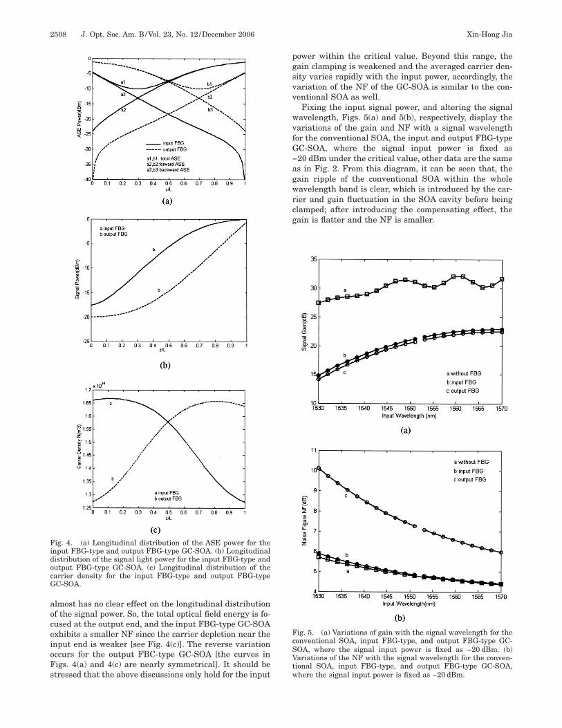
aoceioFs
pgsvv
wvfG−agwrcg
FidocG
FcSVtw
2508 J. Opt. Soc. Am. B/Vol. 23, No. 12 /December 2006 Xin-Hong Jia
lmost has no clear effect on the longitudinal distributionf the signal power. So, the total optical field energy is fo-used at the output end, and the input FBG-type GC-SOAxhibits a smaller NF since the carrier depletion near thenput end is weaker [see Fig. 4(c)]. The reverse variationccurs for the output FBC-type GC-SOA [the curves inigs. 4(a) and 4(c) are nearly symmetrical]. It should betressed that the above discussions only hold for the input
ig. 4. (a) Longitudinal distribution of the ASE power for thenput FBG-type and output FBG-type GC-SOA. (b) Longitudinalistribution of the signal light power for the input FBG-type andutput FBG-type GC-SOA. (c) Longitudinal distribution of thearrier density for the input FBG-type and output FBG-typeC-SOA.
ower within the critical value. Beyond this range, theain clamping is weakened and the averaged carrier den-ity varies rapidly with the input power, accordingly, theariation of the NF of the GC-SOA is similar to the con-entional SOA as well.
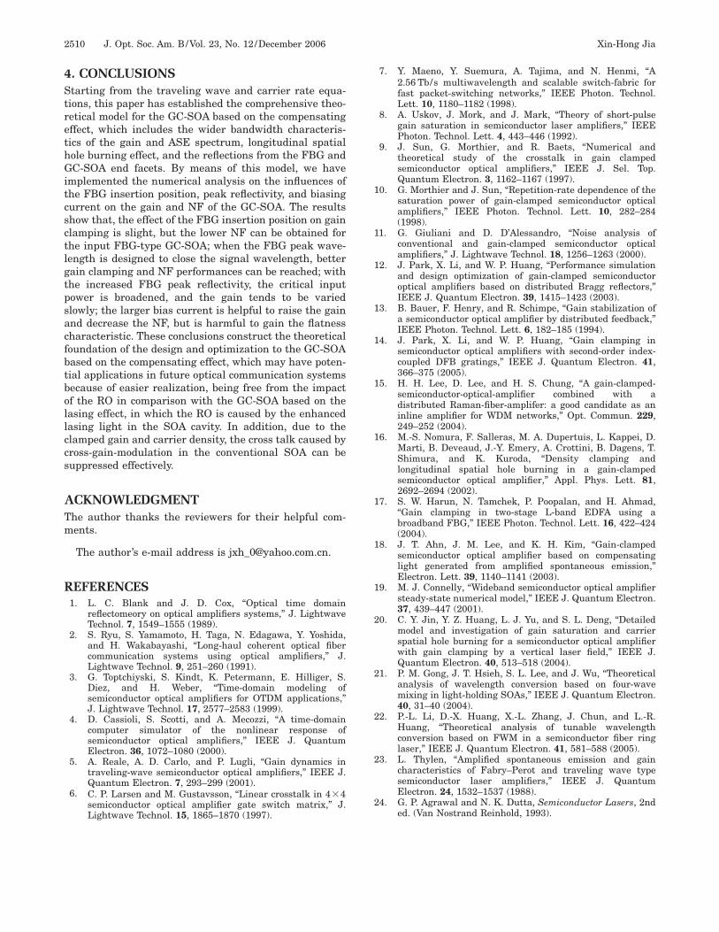
Fixing the input signal power, and altering the signalavelength, Figs. 5(a) and 5(b), respectively, display theariations of the gain and NF with a signal wavelengthor the conventional SOA, the input and output FBG-typeC-SOA, where the signal input power is fixed as20 dBm under the critical value, other data are the sames in Fig. 2. From this diagram, it can be seen that, theain ripple of the conventional SOA within the wholeavelength band is clear, which is introduced by the car-
ier and gain fluctuation in the SOA cavity before beinglamped; after introducing the compensating effect, theain is flatter and the NF is smaller.
ig. 5. (a) Variations of gain with the signal wavelength for theonventional SOA, input FBG-type, and output FBG-type GC-OA, where the signal input power is fixed as −20 dBm. (b)ariations of the NF with the signal wavelength for the conven-ional SOA, input FBG-type, and output FBG-type GC-SOA,here the signal input power is fixed as −20 dBm.

BoAAFwflid0rvpditTobg
cGtpvtvwiSdabstmrs
CGFttuwbalmitdbtllF
F
FFou
Xin-Hong Jia Vol. 23, No. 12 /December 2006 /J. Opt. Soc. Am. B 2509
. Influence of the Fiber Bragg Grating Peak Reflectivityn the Gain-Clamped Semiconductor Opticalmplifier Performancefter considering the smaller noise figure for the inputBG-type GC-SOA, in Fig. 6, the variations of its gainith the input power for the various equivalent peak re-ectivities are given, where the used data are the same as
n Fig. 2. Under the system parameter given above, thisiagram indicates that, for peak reflectivity taken to be.1, the critical input power is �−11 dBm, and the gainipple is �5 dB for the input power under the criticalalue; but for peak reflectivity up to 0.9, the critical inputower is increased to �−3 dBm, while the gain ripplerops to �2 dB. The above analyses imply that, the widernput dynamic range and enhanced gain flat characteris-ic can be obtained by selecting larger peak reflectivity.he reason is that, for larger peak reflectivity, as a resultf the increased total ASE power, the compensating effectetween the signal and the ASE is intensified, and theain clamping is also strengthened.
From Fig. 6, it can also be observed that, with the in-reased FBG peak reflectivity, the gain variation of theC-SOA tends to be more and more smooth, which shows
hat the gain clamping can be achieved as long as the ASEower within the FBG bandwidth is augmented to somealue; it has no clear effect on the gain clamping to con-inue to increase the ASE power after exceeding thisalue. In other words, the ASE within the FBG band-idth acts as a seed light. The effect of the peak reflectiv-
ty on the NF characteristics of the input FBG-type GC-OA, though not shown here, shows no obviousifference. Also, the simulation to the gain and NF char-cteristics of the GC-SOA for various FBG reflectionandwidths were performed, which displays the similarmooth variation with the effect of the FBG peak reflec-ivity. In fact, as confirmed from Fig. 3, it is the induce-ent function by the ASE inside the FBG bandwidth that
esults in the automatic compensating effect between theignal and the ASE within the overall gain bandwidth.
ig. 6. Variations of gain with the input power for the inputBG-type GC-SOA for various equivalent peak reflectivities.
. Influence of the Biasing Current on theain-Clamped Semiconductor Optical Amplifierigures 7(a) and 7(b), respectively, plot the variations of
he gain and NF with the input power for the input FBG-ype GC-SOA under various biasing currents, where thesed data are the same as in Fig. 2. It can be found that,ith the increased biasing current, the signal gain risesecause of the supplemented averaged carrier number,nd the falling spontaneous emission inversion factoreads to the decreased NF. Furthermore, the gain ripple is
ore and more intense. Since the larger biasing currentncreases, both photons and carriers this causes the dras-ic fluctuation of the carriers along the SOA active layeruring their interaction. This longitudinal spatial holeurning16 can lead to considerable gain fluctuation. Fromhe practical point of view, the ideal gain clamping andower NF can be acquired only if the biasing current is se-ected appropriately.
ig. 7. (a) Variations of gain with the input power for the inputBG-type GC-SOA under various biasing currents. (b) Variationsf the NF with the input power for the input FBG-type GC-SOAnder various biasing currents.
4StrethGitcsctlgtpsacfbtbollccs
ATm
R
1
1
1
1
1
1
1
1
1
1
2
2
2
2
2
2510 J. Opt. Soc. Am. B/Vol. 23, No. 12 /December 2006 Xin-Hong Jia
. CONCLUSIONStarting from the traveling wave and carrier rate equa-ions, this paper has established the comprehensive theo-etical model for the GC-SOA based on the compensatingffect, which includes the wider bandwidth characteris-ics of the gain and ASE spectrum, longitudinal spatialole burning effect, and the reflections from the FBG andC-SOA end facets. By means of this model, we have
mplemented the numerical analysis on the influences ofhe FBG insertion position, peak reflectivity, and biasingurrent on the gain and NF of the GC-SOA. The resultshow that, the effect of the FBG insertion position on gainlamping is slight, but the lower NF can be obtained forhe input FBG-type GC-SOA; when the FBG peak wave-ength is designed to close the signal wavelength, betterain clamping and NF performances can be reached; withhe increased FBG peak reflectivity, the critical inputower is broadened, and the gain tends to be variedlowly; the larger bias current is helpful to raise the gainnd decrease the NF, but is harmful to gain the flatnessharacteristic. These conclusions construct the theoreticaloundation of the design and optimization to the GC-SOAased on the compensating effect, which may have poten-ial applications in future optical communication systemsecause of easier realization, being free from the impactf the RO in comparison with the GC-SOA based on theasing effect, in which the RO is caused by the enhancedasing light in the SOA cavity. In addition, due to thelamped gain and carrier density, the cross talk caused byross-gain-modulation in the conventional SOA can beuppressed effectively.
CKNOWLEDGMENThe author thanks the reviewers for their helpful com-ents.
The author’s e-mail address is [email protected].
EFERENCES1. L. C. Blank and J. D. Cox, “Optical time domain
reflectomeory on optical amplifiers systems,” J. LightwaveTechnol. 7, 1549–1555 (1989).
2. S. Ryu, S. Yamamoto, H. Taga, N. Edagawa, Y. Yoshida,and H. Wakabayashi, “Long-haul coherent optical fibercommunication systems using optical amplifiers,” J.Lightwave Technol. 9, 251–260 (1991).
3. G. Toptchiyski, S. Kindt, K. Petermann, E. Hilliger, S.Diez, and H. Weber, “Time-domain modeling ofsemiconductor optical amplifiers for OTDM applications,”J. Lightwave Technol. 17, 2577–2583 (1999).
4. D. Cassioli, S. Scotti, and A. Mecozzi, “A time-domaincomputer simulator of the nonlinear response ofsemiconductor optical amplifiers,” IEEE J. QuantumElectron. 36, 1072–1080 (2000).
5. A. Reale, A. D. Carlo, and P. Lugli, “Gain dynamics intraveling-wave semiconductor optical amplifiers,” IEEE J.Quantum Electron. 7, 293–299 (2001).
6. C. P. Larsen and M. Gustavsson, “Linear crosstalk in 4�4semiconductor optical amplifier gate switch matrix,” J.
Lightwave Technol. 15, 1865–1870 (1997).7. Y. Maeno, Y. Suemura, A. Tajima, and N. Henmi, “A2.56 Tb/s multiwavelength and scalable switch-fabric forfast packet-switching networks,” IEEE Photon. Technol.Lett. 10, 1180–1182 (1998).
8. A. Uskov, J. Mork, and J. Mark, “Theory of short-pulsegain saturation in semiconductor laser amplifiers,” IEEEPhoton. Technol. Lett. 4, 443–446 (1992).
9. J. Sun, G. Morthier, and R. Baets, “Numerical andtheoretical study of the crosstalk in gain clampedsemiconductor optical amplifiers,” IEEE J. Sel. Top.Quantum Electron. 3, 1162–1167 (1997).
0. G. Morthier and J. Sun, “Repetition-rate dependence of thesaturation power of gain-clamped semiconductor opticalamplifiers,” IEEE Photon. Technol. Lett. 10, 282–284(1998).
1. G. Giuliani and D. D’Alessandro, “Noise analysis ofconventional and gain-clamped semiconductor opticalamplifiers,” J. Lightwave Technol. 18, 1256–1263 (2000).
2. J. Park, X. Li, and W. P. Huang, “Performance simulationand design optimization of gain-clamped semiconductoroptical amplifiers based on distributed Bragg reflectors,”IEEE J. Quantum Electron. 39, 1415–1423 (2003).
3. B. Bauer, F. Henry, and R. Schimpe, “Gain stabilization ofa semiconductor optical amplifier by distributed feedback,”IEEE Photon. Technol. Lett. 6, 182–185 (1994).
4. J. Park, X. Li, and W. P. Huang, “Gain clamping insemiconductor optical amplifiers with second-order index-coupled DFB gratings,” IEEE J. Quantum Electron. 41,366–375 (2005).
5. H. H. Lee, D. Lee, and H. S. Chung, “A gain-clamped-semiconductor-optical-amplifier combined with adistributed Raman-fiber-amplifer: a good candidate as aninline amplifier for WDM networks,” Opt. Commun. 229,249–252 (2004).
6. M.-S. Nomura, F. Salleras, M. A. Dupertuis, L. Kappei, D.Marti, B. Deveaud, J.-Y. Emery, A. Crottini, B. Dagens, T.Shimura, and K. Kuroda, “Density clamping andlongitudinal spatial hole burning in a gain-clampedsemiconductor optical amplifier,” Appl. Phys. Lett. 81,2692–2694 (2002).
7. S. W. Harun, N. Tamchek, P. Poopalan, and H. Ahmad,“Gain clamping in two-stage L-band EDFA using abroadband FBG,” IEEE Photon. Technol. Lett. 16, 422–424(2004).
8. J. T. Ahn, J. M. Lee, and K. H. Kim, “Gain-clampedsemiconductor optical amplifier based on compensatinglight generated from amplified spontaneous emission,”Electron. Lett. 39, 1140–1141 (2003).
9. M. J. Connelly, “Wideband semiconductor optical amplifiersteady-state numerical model,” IEEE J. Quantum Electron.37, 439–447 (2001).
0. C. Y. Jin, Y. Z. Huang, L. J. Yu, and S. L. Deng, “Detailedmodel and investigation of gain saturation and carrierspatial hole burning for a semiconductor optical amplifierwith gain clamping by a vertical laser field,” IEEE J.Quantum Electron. 40, 513–518 (2004).
1. P. M. Gong, J. T. Hsieh, S. L. Lee, and J. Wu, “Theoreticalanalysis of wavelength conversion based on four-wavemixing in light-holding SOAs,” IEEE J. Quantum Electron.40, 31–40 (2004).
2. P.-L. Li, D.-X. Huang, X.-L. Zhang, J. Chun, and L.-R.Huang, “Theoretical analysis of tunable wavelengthconversion based on FWM in a semiconductor fiber ringlaser,” IEEE J. Quantum Electron. 41, 581–588 (2005).
3. L. Thylen, “Amplified spontaneous emission and gaincharacteristics of Fabry–Perot and traveling wave typesemiconductor laser amplifiers,” IEEE J. QuantumElectron. 24, 1532–1537 (1988).
4. G. P. Agrawal and N. K. Dutta, Semiconductor Lasers, 2nded. (Van Nostrand Reinhold, 1993).