thermal design considerations for tas5805m class-d audio
TRANSCRIPT
1SLAA880–January 2019Submit Documentation Feedback
Copyright © 2019, Texas Instruments Incorporated
Thermal design considerations for TAS5805M Class-D audio amplifier
Application ReportSLAA880–January 2019
Thermal design considerations for TAS5805M Class-Daudio amplifier
Ella Zhang, Jacky Wang
ABSTRACTThe TAS5805M is a high-efficiency, stereo, closed-loop Class-D audio amplifier that can be used in manyapplications such as Smart Speakers, televisions, and so forth. In some real use cases, there are stillthermal problems in large-output power situations if the design is not carefully considered. Properparameter selection is critical to meet the desired thermal performance in the customer's applications. Thisapplication report discusses some key factors to be considered in the TAS5805M thermal design, such asswitching frequency, modulation modes, and PCB layout.
Contents1 Class-D Audio Amplifier Overview......................................................................................... 22 Power Losses Considerations in Class-D Audio Amplifier ............................................................ 33 PCB Layout Considerations............................................................................................... 104 Summary .................................................................................................................... 125 References .................................................................................................................. 12
List of Figures
1 Typical Block Diagram of Class-D Audio Amplifier...................................................................... 22 Explanation for MOSFET Switching Loss ................................................................................ 33 Explanation for MOSFET Gate Loss ...................................................................................... 44 Efficiency vs. Output Power in Different Switching Frequency (BD Mode) .......................................... 45 PWM Voltage Waveform (50% Duty-Cycle).............................................................................. 56 PWM Voltage Waveform (50% Duty-Cycle).............................................................................. 57 PWM Voltage Waveform (50% Duty-Cycle).............................................................................. 68 PWM Voltage Waveform (50% Duty-Cycle).............................................................................. 69 1SPW Mode in Large Output Condition .................................................................................. 710 Efficiency vs. Output Power with Different Modulation Mode (Fsw = 768 kHz) ..................................... 811 Efficiency vs. Output Power with Different PVDD (1SPW Mode) ..................................................... 812 Efficiency vs. Output Power with Different Output Filter (BD mode, Fsw = 384 kHz) .............................. 913 A Good Example of IC Placement ....................................................................................... 1014 An Example of a Radial Cut .............................................................................................. 1115 An Example of a Circular Cut ............................................................................................ 1116 Layout Example of TAS5805M (Stereo BTL with Ferrite Bead) ..................................................... 12

Comparator
+
+±
±
Ramp
Signal In
Demodulate through low-pass
filter
PWM Modulator
Signal Out
Class-D Audio Amplifier Overview www.ti.com
2 SLAA880–January 2019Submit Documentation Feedback
Copyright © 2019, Texas Instruments Incorporated
Thermal design considerations for TAS5805M Class-D audio amplifier
TrademarksPowerPAD is a trademark of Texas Instruments.All other trademarks are the property of their respective owners.
1 Class-D Audio Amplifier OverviewFigure 1 shows the Class-D audio amplifier. This amplifier is a switching amplifier that consists of a pulsewidth modulator, a power stage, and an output filter. The output of a Class-D amplifier is a PWM (pulse-width-modulation) switched signal with duty cycle that is modulated with audio signal. Compared withtraditional Class-AB audio amplifier, the efficiency of the Class-D amplifier has been significantlyimproved. In some real cases, Class-D audio amplifiers still have thermal problems when the design is notgood enough. The thermal performance is mainly influenced by power losses and heat dissipation.
To achieve better thermal performance, the power losses in the Class-D audio amplifier power stage mustbe taken into consideration since the Class-D audio amplifier efficiency is related to MOSFET total powerlosses. These power losses are the results of MOSFET conduction, switching, and gate charge losses.Power loss is mainly correlated with efficiency. Generally speaking, the efficiency of a Class-D audioamplifier is mainly influenced by the output filter and its ripple current, switching frequency, and power lossfrom the power stage.
Heat dissipation is mainly affected by PCB layout. PCB contributes up to 80-90% of heat dissipation forthermally attached devices. The tips of PCB layout for TAS5805M is discussed in this application report.
Figure 1. Typical Block Diagram of Class-D Audio Amplifier
This report uses TAS5805M as an example to discuss thermal design considerations in Class-D audioamplifiers. The report analyzes the thermal problems in TAS5805M from two aspects: power losses andheat dissipation. To reduce power losses, some factors need to be taken into account, such as switchingfrequency, modulation mode, and output filter selection of TAS5805M. Thermal performance is alsorelated to heat dissipation. For better thermal performance, the PCB layout must be designed properly tominimize the thermal impedance and achieve the best balance of thermal and electrical electromagneticperformance.

� �gate GS SW G TOTP V Q¦ u u
� �GS2 GDSW IN OUT SW¦
I
Q QP =V I
�u u u
www.ti.com Power Losses Considerations in Class-D Audio Amplifier
3SLAA880–January 2019Submit Documentation Feedback
Copyright © 2019, Texas Instruments Incorporated
Thermal design considerations for TAS5805M Class-D audio amplifier
2 Power Losses Considerations in Class-D Audio Amplifier
2.1 PWM Control Scheme ConsiderationsThe Class-D audio amplifier is a switching amplifier that consists of a pulse width modulator. When talkingabout PWM control scheme in TAS5805M, there are two main factors to be considered:• PWM switching frequency• Modulation mode
Different selections of switching frequency and modulation mode influences MOSFET power losses andripple current flowing through LC filter. Large inductor ripple current causes power losses in inductor DCRand decreases efficiency accordingly.
2.2 PWM Switching Frequency SelectionIn the Class-D audio amplifier, PWM switching frequency mainly influences the MOSFET losses andinductor losses. To achieve higher efficiency, MOSFET losses must be taken into consideration.MOSFET-related power loss is composed of conduction loss, switching loss, and gate-drive loss. Theconduction loss is mainly related to Rdson of the MOSFET in the Class D audio amplifier. The conductionloss is independent with switching frequency, but switching loss and gate-drive loss increase linearly withincreasing switching frequency. It takes a finite amount of time for the MOSFET to turn on and off.Figure 2 shows that the switching loss comes from the dynamic voltages and currents, which theMOSFETs must handle during the time it takes to turn on or off. Equation 1 shows that the MOSFETswitching losses are a function of load current, power supply, and switching frequency.
(1)
Where VIN = VDS (drain-to-source voltage), IOUT = ID (drain current), fsw is the switching frequency, QGS2and QGD depend on the time the driver takes to charge the MOSFET, and I is the gate current
Figure 2. Explanation for MOSFET Switching Loss
Figure 3 shows that the MOSFET gate losses are caused by the energy required to charge and dischargethe MOSFET gate. These are both turn-on and turn-off gate losses. Equation 2 shows that the gate drivelosses are frequency dependent and are also a function of the gate capacitance of the MOSFETs. Whenturning the MOSFET on and off, the higher the switching frequency, the higher the gate-drive losses.Gate-drive losses are another reason why efficiency decreases as the switching frequency increases.
(2)
Where the QG(TOT) is the turn-on and turn-off gate losses. VGS is the drain-to-source voltage.

Output power (W)
Effi
cien
cy
0 5 10 15 20 250
10%
20%
30%
40%
50%
60%
70%
80%
90%
fbd-
768 kHz384 kHz
Charging/DischargingGate Capactitance
Power Losses Considerations in Class-D Audio Amplifier www.ti.com
4 SLAA880–January 2019Submit Documentation Feedback
Copyright © 2019, Texas Instruments Incorporated
Thermal design considerations for TAS5805M Class-D audio amplifier
Figure 3. Explanation for MOSFET Gate Loss
Besides the MOSFET losses, the switching frequency also influences the ripple current flow through thepost LC filter. The ripple current causes power losses in the inductor. Higher switching frequency meansyou need a smaller inductor value and a lower ripple current in the inductor. Switching frequency bothinfluences ripple losses and MOSFET losses. When talking about power losses, consider which is themajor factor in the current situation, the MOSFET losses or the ripple current.
At free-air room temperature 25°C, the following measurements are made using TAS5805M EVM board.Output power is measured by Audio Precision. All measurements are taken with PVDD = 16 V, speakerload = 6 Ω. The device PWM frequency is set to 384 kHz and 768 kHz, respectively, in BD Modulation.Spread Spectrum is enabled. The output filter is configured as LC filter (10 µH+0.68 µF). Figure 4 showsthe test results.
Figure 4 shows that when output power is greater than about 14 W, the efficiency of 384 kHz is higherthan 768 kHz. When output power is small, the power losses are mainly dominated by ripple current as768 kHz switching frequency has smaller ripple current than 384 kHz, and the efficiency are higher too.When output power is large, the power losses are mainly dominated by MOSFET losses, and switchinglosses are smaller with lower switching frequency.
Figure 4. Efficiency vs. Output Power in Different Switching Frequency (BD Mode)

peak _ currentSW
PVDDI
8 L ¦
u u
peak _ currentSW
PVDD / 2 1I
L 4 ¦ u
u
peak _ currentPVDD / 2
I tL
G
-0.5*PVDD
0.5*PVDD
0 V
PVDD
0.5*PVDD
0 V
www.ti.com Power Losses Considerations in Class-D Audio Amplifier
5SLAA880–January 2019Submit Documentation Feedback
Copyright © 2019, Texas Instruments Incorporated
Thermal design considerations for TAS5805M Class-D audio amplifier
2.3 Modulation Mode SelectionDifferent modulation modes also influence Class-D audio amplifier efficiency. TAS5805M has threedifferent modulation modes:• BD modulation• 1SPW modulation• Hybrid modulation
In BD mode, Class-D audio amplifiers produce a common-mode voltage of PVDD/2 after the L-C filter atidle status, which is the average value of the 50% duty-cycle PWM switching waveform in the BTL, asshown in Figure 5. The maximum voltage across the inductor is PVDD / 2 and the minimum voltage isminus PVDD / 2. Figure 6 shows the inductor voltage and current waveforms. In traditional Class-D audioamplifiers, it is typically necessary to pass the modulated PWM signal through a low pass filter to extractthe audio content. The low pass filter generally consists of a series inductor and a capacitor to ground. Intraditional Class-D audio amplifiers the positive (OUT+) and the negative (OUT–) outputs are always outof phase, with 50% duty cycle when no input signal is applied. As a result, the full output voltage is appliedto the load at all times, producing relatively high current and high power dissipation in the load if no filter isused.
Figure 5. PWM Voltage Waveform (50% Duty-Cycle)
Figure 6. PWM Voltage Waveform (50% Duty-Cycle)
Use Equation 3, Equation 4, and Equation 5 to find the peak ripple current in BD mode at idle status.
(3)
(4)
(5)
The 1SPW mode alters the BD modulation scheme in order to achieve higher efficiency with a slightdefect in THD+N. In Low Idle Current mode, the outputs operate at approximately 17% modulation duringidle conditions. When an audio signal is applied, one output decreases and one increases. Thedecreasing output signal quickly rails to ground. The result is that only one output is switching during amajority of the audio cycle. Efficiency is improved in this mode due to the reduction of switching losses.The duty-cycle is lower in 1SPW mode than in BD mode. For example, if you use the 15% duty-cycle, thecommon-mode voltage after the LC filter is 0.15 × PVDD, as shown in Figure 7. Figure 8 shows themaximum voltage across the inductor is 0.85 × PVDD and the minimum voltage is –0.15 × PVDD.

peak _ currentSW
51 PVDDI
800 L ¦
u
peak_currentSW
0.85 PVDD 1I = 0.075
L ¦
uu
peak_current0.85 PVDD
I = tLu
G
0.85*PVDD
0 V
0.15*PVDD -1
+1
0 A
0.075/Fsw
PVDD
0 V
0.15*PVDD
Power Losses Considerations in Class-D Audio Amplifier www.ti.com
6 SLAA880–January 2019Submit Documentation Feedback
Copyright © 2019, Texas Instruments Incorporated
Thermal design considerations for TAS5805M Class-D audio amplifier
Figure 7. PWM Voltage Waveform (50% Duty-Cycle)
Figure 8. PWM Voltage Waveform (50% Duty-Cycle)
Use Equation 6, Equation 7, and Equation 8to find the peak ripple current in 1SPW mode at idle.
(6)
(7)
(8)
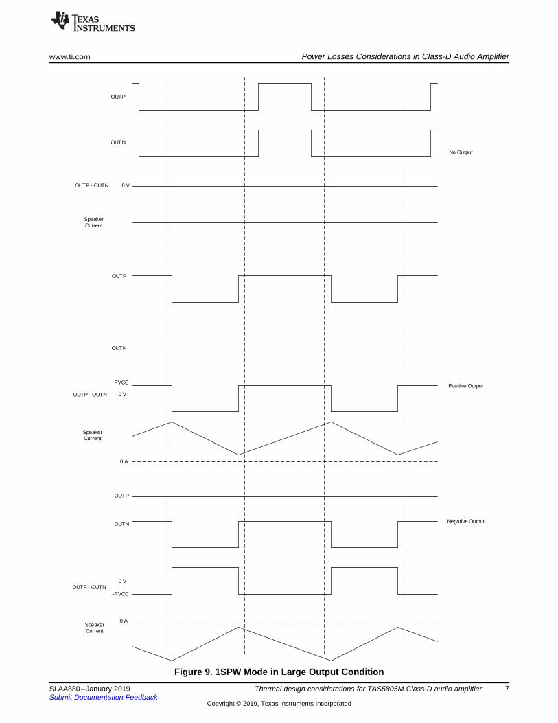
The 1SPW mode has lower ripple current on the inductors than BD mode and makes higher efficiency.Figure 9 shows one of the OUTP and OUTN stops switching during large output condition in 1SPW mode.The result is that only one output is switching during a majority of the audio cycle. Efficiency is alsoimproved in this mode due to the reduction of switching losses.
OUTP
OUTN
0 V
OUTP
OUTN
PVCC
0 V
0 A
OUTP
OUTN
-PVCC
0 A
0 V
OUTP - OUTN
SpeakerCurrent
OUTP - OUTN
SpeakerCurrent
SpeakerCurrent
OUTP - OUTN
Negative Output
Positive Output
No Output
www.ti.com Power Losses Considerations in Class-D Audio Amplifier
7SLAA880–January 2019Submit Documentation Feedback
Copyright © 2019, Texas Instruments Incorporated
Thermal design considerations for TAS5805M Class-D audio amplifier
Figure 9. 1SPW Mode in Large Output Condition

Output Power (W)
Effi
cien
cy (
%)
0 5 10 15 20 250
10%
20%
30%
40%
50%
60%
70%
80%
90%
fbd-
PVDD=12 VPVDD=16 VPVDD=24 V
Output Power (W)
Effi
cien
cy
0 5 10 15 20 250
10%
20%
30%
40%
50%
60%
70%
80%
90%
fbd-
1SPWBD
Power Losses Considerations in Class-D Audio Amplifier www.ti.com
8 SLAA880–January 2019Submit Documentation Feedback
Copyright © 2019, Texas Instruments Incorporated
Thermal design considerations for TAS5805M Class-D audio amplifier
Figure 10 compares the efficiency of different modulation mode. The result is tested with LC filter (10 µH +0.68 µF) and the switching frequency is 768 kHz. The 1SPW mode has lower ripple current on theinductors than BD mode in idle condition and makes higher efficiency. Only one output is switching duringthe majority of the audio cycle in a large output condition, therefore, it can also improve the efficiency.
Figure 10. Efficiency vs. Output Power with Different Modulation Mode (Fsw = 768 kHz)
Figure 11 shows PVDD, which is an important factor for thermal design. The efficiency of TAS5805Mdecreases with the increase of PVDD. When PVDD > 19 V, use 1SPW rather than BD, considering theefficiency. In summary, the efficiency of 1SPW is higher than BD mode and it is suggested you choose1SPW mode in large output condition. In addition, a larger load means better efficiency.
Figure 11. Efficiency vs. Output Power with Different PVDD (1SPW Mode)
2.4 Output Filter SelectionSwitching outputs of Class-D audio amplifiers produce harmonics that extend to several hundred MHz, butthe Federal Communications Commission (FCC) has imposed limits on radiated emissions at frequenciesbetween 30 MHz and 1 GHz. It is necessary to filter a Class-D amplifier output to comply with ElectroMagnetic Compliance, or EMC. Ferrite beads and LC filter can be used to meet the FCC limits in theTAS5805M. In many cases, ferrite bead filters can attenuate the high frequencies in the output of Class-Daudio amplifiers, but ferrite beads have little effect on lower frequency signals. The load has the full PWMsignal across its terminals, causing a high-frequency current to pass through the load, which leads to highpower dissipation and thermal problem. To meet the FCC limits and reduce power dissipation, it is highlyrecommended to choose lower switching frequency (384 kHz) and BD mode in ferrite bead cases.
In LC filter cases, speaker impedance includes inductance, but it is primarily resistive, whereas an LC filteris almost purely reactive. An LC filter with a cutoff frequency less than the Class-D switching frequencyallows the switching current to flow in the filter instead of the load. The filter has less resistance but higherimpedance at the switching frequency than the speaker, resulting in less power dissipation, thereforeincreasing efficiency.

Output Power (W)
Effi
cien
cy (
%)
0 5 10 15 20 250
10%
20%
30%
40%
50%
60%
70%
80%
90%
fbd-
di Vdt L
www.ti.com Power Losses Considerations in Class-D Audio Amplifier
9SLAA880–January 2019Submit Documentation Feedback
Copyright © 2019, Texas Instruments Incorporated
Thermal design considerations for TAS5805M Class-D audio amplifier
Ripple current is defined as the alternating current flowing through the output inductor of a Class-Damplifier. If LC filter is not designed properly, it also causes a large current to pass through the load, whichleads to high power dissipation, poor efficiency, and potential speaker damage. High power dissipationcauses thermal problems. In a BTL configuration, the total power dissipation due to the ripple current mustbe considered for both sides of the output bridge. The ripple current through an inductor is defined as:
where• di /dt = rate of change in inductor current• V = voltage across the inductor• L = inductance (9)
Equation 9 shows that the larger value inductors in the output filter make lower ripple current. Lower ripplecurrent is desired in BD modulation amplifiers to reduce loss across the RDS (of the output FETs and theDCR of the output inductors on). Inductor DCR is the series electrical resistance of the wire used to makethe windings in an inductor. Although the DCR is usually low, at high output current, the DCR cancontribute considerable power losses for the audio signal. In 384 kHz switching frequency, it isrecommended that choose at least 10 µH inductor in LC filter. See the LC Filter Design application reportfor details. Increasing the inductance reduces the output ripple current, and better efficiency is generallyobserved. With 384 kHz switching frequency, select 22 µH + 0.68 µF or 15 µH + 0.68 µF or 10 µH + 0.68µF as the output filter (Speaker Load = 8 Ω/6 Ω), this helps reduce power dissipation. When choosing 768kHz as the TAS5805M switching frequency, you can choose a smaller inductor value during the inductorselection. It is highly recommended to select 10 µH + 0.68 µF or 4.7 µH +0.68 µF as the output filter.
The output filter also influences the efficiency of TAS5805M, as shown in Figure 12. The TAS5805M is setto 384 kHz and BD mode. Ferrite beads cause a high-frequency current to pass through the load, whichleads to high power dissipation and thermal problem. An LC filter allows the switching current to flow inthe filter instead of the load and has better thermal performance. To achieve better thermal performance, itis highly recommended that use LC filter as output filter when the output power is larger than 210 W. Ferritebeads are often used in portable device with small output power.
Figure 12. Efficiency vs. Output Power with Different Output Filter (BD mode, Fsw = 384 kHz)

PCB Layout Considerations www.ti.com
10 SLAA880–January 2019Submit Documentation Feedback
Copyright © 2019, Texas Instruments Incorporated
Thermal design considerations for TAS5805M Class-D audio amplifier
3 PCB Layout ConsiderationsCompared with Class-AB audio amplifier, the efficiency of the Class-D amplifier has significantly improved.When the output power of Class D audio amplifier is large, there can be a thermal problem in certaincircumstances. Device performance can be affected by high temperature, so it is important to understandand control the temperature during operation. The goal of the PCB design is to minimize the thermalimpedance. The following tips must be followed to achieve better thermal performance:• Avoid placing other heat producing components or structures near the amplifier.• If possible, use a higher layer count PCB to provide more heat sinking capability for the device.• Thickness of copper and layers of PCB have great effect on thermal performance. For the EVM board,
it is 4 layers and 2Oz copper.
Place the Class-D audio amplifier away from the edge of the PCB when possible to ensure that the heatcan travel away from the device on all four sides. In a soldered PowerPAD™ device, the heat travels fromthe die, through the die attach, to the die pad, through the solder and into the PCB where it is dissipatedinto the air. Center the IC in the ground plane and ground the PowerPAD with thermal vias. Figure 13shows you an example of the correct placement. The thermal vias creates low thermal resistance from thePowerPAD to the ground plane for best heat transfer. With the IC centered, all paths through PCB copperfor heat have reasonably low thermal resistance and good thermal radiating area.
Figure 13. A Good Example of IC Placement
Avoid cutting off the flow of heat from the Class D audio amplifier to the surrounding areas with traces orstrings. Radial or nearly radial cuts allow heat to flow, as shown in Figure 14. Radial or nearly radial cutsdo not block paths for heat. They let heat flow between them, away from the IC. A circular cut disconnectsthe copper inside the cut from the copper outside the cut.

www.ti.com PCB Layout Considerations
11SLAA880–January 2019Submit Documentation Feedback
Copyright © 2019, Texas Instruments Incorporated
Thermal design considerations for TAS5805M Class-D audio amplifier
Figure 14. An Example of a Radial Cut
Heat flow to the copper outside the circular cut is reduced, so the copper outside cannot conduct muchheat. A circular cut increases thermal resistance of the PCB and makes the IC run hotter, as shown inFigure 15.
Figure 15. An Example of a Circular Cut

Summary www.ti.com
12 SLAA880–January 2019Submit Documentation Feedback
Copyright © 2019, Texas Instruments Incorporated
Thermal design considerations for TAS5805M Class-D audio amplifier
For the TAS5805M thermal pad, which connects electrically and thermally to the PowerPAD™ of theTAS5805M device, it is important that it is big enough for heat to pass. By increasing the number of vias,as shown in the Figure 16, we can improve thermal performance of the TAS5805M. The vias can carry theheat from the device through to the layers of the PCB. Vias is present a low thermal-impedance path fromthe device into the PCB. Then, the heat travels away from the device and into the surrounding structuresand air. Vias must be arranged in columns, which extend in a line radially from the heat source to thesurrounding area. Ensure that vias do not cut off power current flow from the power supply through theplanes on internal layers. If needed, remove some vias that are farthest from the TAS5805M device toopen up the current path to and from the device.
Figure 16. Layout Example of TAS5805M (Stereo BTL with Ferrite Bead)
4 SummaryThe TAS5805M is a high-efficiency Class-D audio amplifier, but there are still thermal problems in largeoutput power situations. The efficiency of a TAS5805M is mainly influenced by the output filter, switchingfrequency and PCB layout. Points to be remembered to achieve better thermal performance:• In a Class-D audio amplifier, PWM switching frequency mainly influences the MOSFET losses and
inductor losses. Lower PWM switching frequency with large inductor to improve thermal performance.• LC filter can achieve better thermal performance than Ferrite Bead in large output situation.• Place the TAS5805M device away from the edge of the PCB and avoid cutting off the flow of heat from
the TAS5805M device to the surrounding areas with traces or via strings.
5 References• TAS5805M 23-W, Inductor-Less, Digital Input, Stereo, Closed-Loop Class-D Audio A data sheet• Minimize Idle Current in Portable Audio With TAS5805M Hybrid Mode application report• LC Filter Design application report• Filter-Free™ Class-D Audio Amplifiers application report

IMPORTANT NOTICE AND DISCLAIMER
TI PROVIDES TECHNICAL AND RELIABILITY DATA (INCLUDING DATASHEETS), DESIGN RESOURCES (INCLUDING REFERENCEDESIGNS), APPLICATION OR OTHER DESIGN ADVICE, WEB TOOLS, SAFETY INFORMATION, AND OTHER RESOURCES “AS IS”AND WITH ALL FAULTS, AND DISCLAIMS ALL WARRANTIES, EXPRESS AND IMPLIED, INCLUDING WITHOUT LIMITATION ANYIMPLIED WARRANTIES OF MERCHANTABILITY, FITNESS FOR A PARTICULAR PURPOSE OR NON-INFRINGEMENT OF THIRDPARTY INTELLECTUAL PROPERTY RIGHTS.These resources are intended for skilled developers designing with TI products. You are solely responsible for (1) selecting the appropriateTI products for your application, (2) designing, validating and testing your application, and (3) ensuring your application meets applicablestandards, and any other safety, security, or other requirements. These resources are subject to change without notice. TI grants youpermission to use these resources only for development of an application that uses the TI products described in the resource. Otherreproduction and display of these resources is prohibited. No license is granted to any other TI intellectual property right or to any thirdparty intellectual property right. TI disclaims responsibility for, and you will fully indemnify TI and its representatives against, any claims,damages, costs, losses, and liabilities arising out of your use of these resources.TI’s products are provided subject to TI’s Terms of Sale (www.ti.com/legal/termsofsale.html) or other applicable terms available either onti.com or provided in conjunction with such TI products. TI’s provision of these resources does not expand or otherwise alter TI’s applicablewarranties or warranty disclaimers for TI products.
Mailing Address: Texas Instruments, Post Office Box 655303, Dallas, Texas 75265Copyright © 2019, Texas Instruments Incorporated