thermal diodes based on near-field … thermal diodes based on near-field radiation michal lipson...
TRANSCRIPT

AFRL-RY-WP-TR-2015-0163
THERMAL DIODES BASED ON NEAR-FIELD RADIATION Michal Lipson
Cornell University OCTOBER 2015 Final Report
Approved for public release; distribution unlimited. See additional restrictions described on inside pages
STINFO COPY
AIR FORCE RESEARCH LABORATORY SENSORS DIRECTORATE
WRIGHT-PATTERSON AIR FORCE BASE, OH 45433-7320 AIR FORCE MATERIEL COMMAND
UNITED STATES AIR FORCE

NOTICE AND SIGNATURE PAGE
Using Government drawings, specifications, or other data included in this document for any purpose other than Government procurement does not in any way obligate the U.S. Government. The fact that the Government formulated or supplied the drawings, specifications, or other data does not license the holder or any other person or corporation; or convey any rights or permission to manufacture, use, or sell any patented invention that may relate to them. This report is the result of contracted fundamental research deemed exempt from public affairs security and policy review in accordance with SAF/AQR memorandum dated 10 Dec 08 and AFRL/CA policy clarification memorandum dated 16 Jan 09. This report is available to the general public, including foreign nationals. AFRL-RY-WP-TR-2015-0163 HAS BEEN REVIEWED AND IS APPROVED FOR PUBLICATION IN ACCORDANCE WITH ASSIGNED DISTRIBUTION STATEMENT. // Signature// // Signature// MARK J. PACER, Program Manager ROSS W. DETTMER, Chief Devices for Sensing Branch Devices for Sensing Branch Aerospace Components & Subsystems Division Aerospace Components & Subsystems Division // Signature// JASON V. PAUL, MAJOR, USAF Deputy Division Chief Aerospace Components & Subsystems Division Sensors Directorate This report is published in the interest of scientific and technical information exchange, and its publication does not constitute the Government’s approval or disapproval of its ideas or findings. *Disseminated copies will show “//Signature//” stamped or typed above the signature blocks.

REPORT DOCUMENTATION PAGE Form Approved OMB No. 0704-0188
The public reporting burden for this collection of information is estimated to average 1 hour per response, including the time for reviewing instructions, searching existing data sources, searching existing data sources, gathering and maintaining the data needed, and completing and reviewing the collection of information. Send comments regarding this burden estimate or any other aspect of this collection of information, including suggestions for reducing this burden, to Department of Defense, Washington Headquarters Services, Directorate for Information Operations and Reports (0704-0188), 1215 Jefferson Davis Highway, Suite 1204, Arlington, VA 22202-4302. Respondents should be aware that notwithstanding any other provision of law, no person shall be subject to any penalty for failing to comply with a collection of information if it does not display a currently valid OMB control number. PLEASE DO NOT RETURN YOUR FORM TO THE ABOVE ADDRESS.
1. REPORT DATE (DD-MM-YY) 2. REPORT TYPE 3. DATES COVERED (From - To) October 2015 Final 31 January 2014 – 31 July 2015
4. TITLE AND SUBTITLE THERMAL DIODES BASED ON NEAR-FIELD RADIATION
5a. CONTRACT NUMBER FA8650-14-1-7406
5b. GRANT NUMBER
5c. PROGRAM ELEMENT NUMBER 61101E
6. AUTHOR(S)
Michal Lipson 5d. PROJECT NUMBER
1000 5e. TASK NUMBER
N/A 5f. WORK UNIT NUMBER
Y0ZF 7. PERFORMING ORGANIZATION NAME(S) AND ADDRESS(ES) 8. PERFORMING ORGANIZATION
Cornell University 373 Pine Tree Road Ithaca, NY 14850-2820
REPORT NUMBER AFRL-RY-WP-TR-2015-0163
9. SPONSORING/MONITORING AGENCY NAME(S) AND ADDRESS(ES) 10. SPONSORING/MONITORING Air Force Research Laboratory Sensors Directorate Wright-Patterson Air Force Base, OH 45433-7320 Air Force Materiel Command United States Air Force
Defense Advanced Research Projects Agency 675 North Randolph Street Arlington, VA 22203-2114
AGENCY ACRONYM(S) AFRL/RYDD
11. SPONSORING/MONITORING AGENCY REPORT NUMBER(S)
AFRL-RY-WP-TR-2015-0163 12. DISTRIBUTION/AVAILABILITY STATEMENT
Approved for public release; distribution unlimited 13. SUPPLEMENTARY NOTES
This material is based on research sponsored by Air Force Research Laboratory (AFRL) and the Defense Advanced Research Agency (DARPA) under agreement number FA8650-14-1-7406. The U.S. Government is authorized to reproduce and distribute reprints for Governmental purposes notwithstanding any copyright notation thereon. The views and conclusions contained herein are those of the authors and should not be interpreted as necessarily representing the official policies or endorsements, either expressed or implied, of Air Force Research Laboratory (AFRL) and the Defense Advanced Research Agency (DARPA) or the U.S. Government. This report is the result of contracted fundamental research deemed exempt from public affairs security and policy review in accordance with SAF/AQR memorandum dated 10 Dec 08 and AFRL/CA policy clarification memorandum dated 16 Jan 09. Report contains color.
14. ABSTRACT The objectives of this work were to demonstrate a thermal rectification phenomenon: non-reciprocal heat transfer between two structures. This effect could be used to maintain the temperature of a device at a lower temperature than its surrounding, unaffected from neighboring hotspots. We proposed to demonstrate experimentally thermal rectification of >40% based on our recent demonstration of near-field heat transfer. Simulation with alumina, silica and platinum coated nano-beams showing ~65% rectification was achieved. The demonstration of thermal rectification >40% between the two nano-membranes was not achieved but potential avenues identified. The current platform, with slight modifications in the deposited layers on the nano-beam surface, is suitable to obtain required separation for near field heat transfer and eventually thermal rectification of >40%.
15. SUBJECT TERMS
nano-membranes, thermal rectification, diodes, near-field radiation 16. SECURITY CLASSIFICATION OF: 17. LIMITATION
OF ABSTRACT: SAR
18. NUMBER OF PAGES
48
19a. NAME OF RESPONSIBLE PERSON (Monitor) a. REPORT Unclassified
b. ABSTRACT Unclassified
c. THIS PAGE Unclassified
Mark Pacer 19b. TELEPHONE NUMBER (Include Area Code)
N/A Standard Form 298 (Rev. 8-98)
Prescribed by ANSI Std. Z39-18

i Approved for public release; distribution unlimited.
TABLE OF CONTENTS Section Page List of Figures ................................................................................................................................. ii 1.0 Summary and Importance of Main Achievements .............................................................. 1
2.0 Technical Details of Main Achievement ............................................................................. 3
3.0 Milestones Achieved During the Project ........................................................................... 15
4.0 References .......................................................................................................................... 17
Appendix: Publications ................................................................................................................ 18
List of Acronyms, Abbreviations, and Symbols ........................................................................... 43

ii Approved for public release; distribution unlimited.
List of Figures
Figure Page Figure 1: Schematic and Theoretical Prediction ............................................................................ 3 Figure 2: (a) SEMs of the Device and (b) False Color SEM of the Nano-beams Cross Section Prior to Substrate Removal ................................................................................................ 4 Figure 3: (a) Measured Temperature and (b) Heat Transfer Power ............................................... 5 Figure 4: Schematic Representation of the Operation Principle of a Thermal Rectifier ............... 6 Figure 5: (a) Measurement of the Phonon Resonances of SiC and Comparison with Theory and (b) Predicted Surface Energy Density of our Deposited SiC Film, Compared to that of SiO2, which was the Material used in our Previous Platform ......................................... 7 Figure 6: Improved Mechanical Design for Near-field Rectification Measurement ..................... 8 Figure 7: SEM Showing Detrimental Bending of the Device when Fabricated in 130 nm Thick Silicon Carbide ..................................................................................................................... 9 Figure 8: SEM of the Fabricated Device Based on a Si3N4 Mechanical Support Coated with SiC .......................................................................................................................................... 9 Figure 9: Measured MEMS Displacement as a Function of the Voltage on the MEMS Actuators ....................................................................................................................................... 10 Figure 10: (a) Measurement of Near-field Heat Transfer as a Function of the Distance Between the Nano-beams (the far-field limit is included in the inset (log scale)) and (b) Minimum Achieved Gap (red) and Enhancement over Far-field (blue) as a Function of the Heated Beam Temperature ................................................................................................. 11 Figure 11: Normalized Rectification as a Function of Film Thickness for Measured Damping Coefficient of our Polycrystalline SiC (Γ = 9.5 cm-1) ................................................... 12 Figure 12: Heat Transfer between Thin Pt and SiO2 as a Function of Pt Film Thickness for Two Different Temperatures and Normalized by Black Body ............................................... 13 Figure 13: (a) Multilayer Stack of Materials on Two Nano-beam Surfaces for Efficient Heat Transfer and (b) Angled Evaporation of Currently Fabricated Nano-beams to allow the Required Multilayer Stack on the Inner Heat Exchanging Surfaces ...................................... 13 Figure 14: Heat Transfer Spectrum for the Structure Shown in Figure 12a with 40nm Gap ...................................................................................................................................... 14

1 Approved for public release; distribution unlimited.
1.0 Summary and Importance of Main Achievements
In this final report we summarize the work done towards demonstration of rectification, various milestones achieved during the process, and the current status of the work. During the first part of this project we designed and demonstrated a platform for measurement of near-field radiative heat transfer on-chip. A strong on-chip radiative heat transfer was shown using a novel geometrical configuration of two parallel suspended nano-beams with silicon nitride core. The distance between the two nano-beams was tuned electrostatically and the heat transfer was measured using an integrated platinum resistor. We demonstrated 107 nW/K of background heat conduction on the nano-beams, thermally isolated from environment with <20 nm precision in position control. (Milestones achieved: I.1, I.2, I.3, and I.4) Later, in the second part, we performed simulations and found that silicon carbide (SiC) nano-beam could allow near-field rectification of heat transfer. We proposed to coast one of the nano-beam in our design with thin layer of silicon oxide. A thin layer of silicon oxide would induce frequency shift in the silicon carbide surface resonance and provide required asymmetry for thermal rectification. We developed a process for plasma enhanced chemical vapor deposition (PECVD) deposition of SiC and showed that high temperature annealed plasma deposited microcrystalline SiC exhibits phonon resonance at that same frequency as expected for single crystal silicon carbide. However, the plasma resonance of our microcrystalline SiC was found to be three times more damped than its single crystal counterpart. Further, simulations were performed to determine the influence of this damping on the rectification behavior. In the third and fourth part of the project, we performed detailed simulations for heat rectification between nano-beams made of microcrystalline SiC. We also presented an upgraded design of our mechanical platform that is better suited for near-field rectification experiment. The initial design had several limitations like mechanical asymmetries, material stress, lower operating temperature, and broad surface plasmon polarition resonance due to silica coating on nano-beams. These limitations had to be rectified in order to achieve <50 nm gap, avoid performance confusion between thermal rectification and mechanical asymmetries, allow higher temperature capabilities and eventually have efficient thermal rectification. The design, after required rectification, is fabricated using our developed polycrystalline silicon carbide. The fabrication processes are modified to reduce stress bending issues. With the new platform we demonstrate near-field radiative heat transfer that is 82X stronger than the far field limit. (Milestones achieved: II.1, II.2, and II.3) In the last part of the project, measurements for thermal rectification are performed on the new platform having silicon nitride nano-beams coated with thin layer of silicon carbide. Poor rectification is observed and simulations using the experimentally obtained damping rate of surface plasmon resonance for SiC confirm this inefficiency. The simulations show that the rectification for silicon carbide nano-beams is just 7%. Afterwards, we have performed detailed simulations to explore various material platforms and geometries to achieve proposed rectifications efficiency. Simulations show promising results with alumina, silica, and platinum coated silicon nitride nano-beams having 66-80% rectification. This proposed platform requires minimal change in our fabrication procedure developed during the entire project. Alumina,

2 Approved for public release; distribution unlimited.
silica, and platinum can be deposited on our already fabricated silicon nitride nano-beams coated silicon carbide to perform this experiment. (Milestones achieved: III.1 and III.2)

3 Approved for public release; distribution unlimited.
2.0 Technical Details of Main Achievement
We show strong near-field radiative heat transfer in a novel on-chip geometrical configuration of two parallel suspended nano-beams where the distance between the beams can be tuned electrostatically. Our geometrical configuration is shown in Figure 1a while Figure 1c shows a cross section scheme of a mobile and sensing beam. We use silicon dioxide (SiO2) for its surface phonon polariton resonances, at 495 cm-1 and 1160 cm-1, known to allow near-field heat transfer. Silicon nitride (Si3N4) is used solely for mechanical purposes. We use platinum (Pt) resistors both as resistive heaters and as thermometers to measure the amount of heat transfer. The gap between the two nano-beams is tuned using a monolithically integrated micro-electromechanical system (MEMS) actuator (see Figure 1a). Electrostatic actuation is chosen for its negligible power consumption, and hence negligible parasitic heat generation. When an actuation voltage is applied, the electric field across the two actuation capacitors induces an attraction force that brings the suspended part of the actuator closer to the fixed heated beam (see Figure 1b). When this occurs, the heat transfer between the nano-beams is expected to be drastically enhanced as shown in Figure 1d.
Figure 1: Schematic and Theoretical Prediction (a) Schematic (not to scale) and electrical circuit of the two nano-beams system integrated with
the MEMS actuator, (b) Schematic (not to scale) of the MEMS displacement, (c) Schematic representation of heat transfer between two nano-beams – a fixed and a mobile one. At small gap, evanescent surface polariton resonances at the SiO2 surfaces couple to enable near-field
radiative heat transfer between the nano-beams. Si3N4 is used for mechanical purposes, while Pt is used both as a resistive heater and a temperature sensor, (d) Theoretical prediction of the heat
transfer between two nano-beams of 200 µm length, and 500 nm x 1.1 µm cross section. The SiO2 thickness in this case is 100 nm.

4 Approved for public release; distribution unlimited.
The structure is fabricated using conventional nanofabrication processes, which consist of low pressure chemical vapor deposition (LPCVD) of SiO2 and Si3N4, and electron-beam evaporation of platinum resistors and aluminum electrical contacts. The aluminum layer is chosen to be much thicker (250 nm) than the platinum layer (60 nm), such that the resistance of the aluminum contracts is negligible compared with the platinum resistors. The scanning electron micrograph (SEM) images of the device in top view (Figure 2a) and the cross section of the fabricated silicon nitride nano-beams pre-release (Figure 2b) is shown.
Figure 2: (a) SEMs of the Device and (b) False Color SEM of the Nano-beams Cross Section Prior to Substrate Removal
The fabricated MEMS platform is found to allow precise control of the nano-beam displacement over 500 nm with ±10 nm accuracy. Measurements of temperature changes as a function of nano-beam separation clearly indicate that near-field heat transfer is the dominant thermal transport mechanism between the nano-beams. In the heat transfer experiment, the gap between the nano-beams is progressively reduced using the MEMS actuator, while a constant voltage of Vfix = 0.22 V is supplied to heat up the fixed (sensing) nano-beam. The temperatures of both nano-beams calculated from variation of electrical resistance of platinum resistors as a function of their separation distance is shown in Figure 3a. As the gap decreases, the temperature of the fixed heated beam diminishes slightly as it loses heat to the mobile beam. More importantly, the temperature of the mobile sensing beam increases by almost a factor 5 (from Tmob = 3 K to Tmob = 14.7 K). Such increase is a clear indication that as the gap decreases, near-field effects, rather than conduction through the substrate, dominate heat transfer between the nano-beams. The near-field heat transfer power is extracted from our temperature measurements and is found to be 8 times stronger than substrate conduction, and 7 times stronger than the far-field radiation limit. By solving the thermal circuit of the experiment using the knowledge of background heat conduction of the fixed and mobile beams along with the estimated temperature data from Figure 3a, heat transfer between nano-beams is obtained (see Figure 3b). More details related to the experiment and measurement can be found in our publication based on this work [1-2].

5 Approved for public release; distribution unlimited.
Figure 3: (a) Measured Temperature and (b) Heat Transfer Power (a) Measured temperature (relative to room temperature) of the fixed heated beam (Tfix) and the
mobile sensing beam (Tmob) as a function of their separation distance with constant heating voltage supplied to the fixed beam and sensing current to the mobile beam. (b) Heat transfer
power between the nano-beams as a function of their separation distance. Substrate conduction is found to account for less than 15% of the total heat transfer at the smallest gap.
In order to achieve efficient rectification, we need to have a material with narrower surface plasmon resonance. Silicon carbide has been proposed in various theoretical work as a good candidate for thermal rectification platform [3]. Simulations were carried out to understand if silicon carbide nano-beams would allow radiative heat transfer rectification in near-field. For achieving thermal rectification it was found that having silica layer on one of the nano-beam would induce the frequency shift in silicon carbide resonance and ensure the required asymmetry. Thermal rectification mechanism due to misaligned surface plasmon resonance is illustrated schematically in Figure 4.

6 Approved for public release; distribution unlimited.
Figure 4: Schematic Representation of the Operation Principle of a Thermal Rectifier Based on misaligned surface waves between two silica coated silicon carbide nano-beams.
Different oxide coating thicknesses allow for the initial misalignment between the surface waves. In order to be able to fabricate a structure with silicon carbide, we had to develop our expertise for its deposition. We developed a process for PECVD of SiC from silane (SiH4) and methane (CH4) gas precursors, followed by annealing at 1050 oC for 90 minutes. Systematic optimization for refractive index of deposited films was carried out as a function of silane percentage in the mixture. It is found that 4.5% silane in the mixture is the optimum point to achieve minimum refractive index and a stoichiometric film. Away from the optimum point, the refractive index increases for excess silicon and carbon. Refer to earlier quarterly report for more details. We also measured the phonon resonance of our films by recording their infrared transmission spectrum at 70 degree angle of incidence using a Fourier transform infrared spectrometer. As shown in Figure 5a, our film exhibits the same main narrow phonon resonances bands than reported in the literature for single crystal silicon carbide. The experimental peaks are however about three times wider than the theoretical ones. This broadening is most likely a damping effect caused by phonon scattering at the grain boundaries of the microcrystalline film. From this measured phonon resonance, permittivity of our deposited films is extracted which is then used to predict the surface thermal energy spectrum. We have found that surface energy density our deposited SiC is five times narrower than that of silica which could be beneficial to near-field thermal rectification (refer to Figure 5b).

7 Approved for public release; distribution unlimited.
Figure 5: (a) Measurement of the Phonon Resonances of SiC and Comparison with Theory and (b) Predicted Surface Energy Density of our Deposited SiC Film, Compared to that of
SiO2, which was the Material used in our Previous Platform Simulation studies were undertaken to see thermal rectification between silicon carbide nano-beams coated with silica and the effect of resonance damping as seen in measured plasmon resonance. The simulations performed by Sanford, using full 3D finite element modelling show that ideal silica thickness for rectification (at 100 nm separation) is 5 nm, for which we expect 20% rectification. The rectification is found to be linear with temperature, such that a higher temperature bias would allow the targeted 40% rectification. It is observed in the simulations that having silica films thinner than optimum thickness would lead to insufficient shift in surface resonance while, thicker films would lead to attenuation of surface resonance of coated silicon carbide beam. Either of which is detrimental for thermal rectification. In order to perform the rectification experiment with silicon carbide nano-beams coated with thin film of silica we had to improve our mechanical platform presented earlier in the quarterly report. In the earlier described platform, the minimum gap achieved was 250 nm, while ≤100 nm of gap is required to achieve our milestone II.1. The platform also needs to be perfectly symmetric in order to avoid any non-symmetrical effect that could lead to false rectification signal. We also need to achieve temperature as high as 600 K to perform 40% rectification. This is not possible with the current design of platinum resistors having aluminum contact pads that limit higher than 400 K operating temperatures. The new platform design now provides solution to all these issues. The platinum-resistors are now made more resistive by improved geometry and five times wider contacts to reduce contract resistance. The stress induced deformation (see Figure 8 in first quarterly report), is reduced by having perfectly straight and parallel beams to balance material tensile stress which would prevent deformation upon structural release. Also, the nano-beams are now exactly identical with each having a MEMS actuator as opposed to our initial asymmetric design of having a fixed and a mobile beam (see Figure 6). This would save us from measurement contamination due to asymmetrical effects leading to false conclusions.

8 Approved for public release; distribution unlimited.
Figure 6: Improved Mechanical Design for Near-field Rectification Measurement The beams are now perfectly parallel to avoid contract points that prevented closing the gap
below 250 nm with the original platform (see Figure 8 in first quarterly report). The system is also perfectly symmetric, in order to avoid spurious false rectification signals from asymmetries
in the system. Platinum is now the only metal used, such that we should achieve higher temperature than with the previous platform (first quarterly report), which included aluminum.
We proceeded to the first fabrication attempt of the new structure design presented above in Figure 6. At first, a thin film microcrystalline silicon carbide (130 nm) is deposited on a silicon wafer with our developed process followed by annealing and then patterning in fluorine chemistry. The platinum electrical circuitry is then made on top using chrome as adhesion layer. Finally, a 5 nm thin silica layer is deposited on one of the nano-beams to enable rectification capability. Although we could successfully fabricate and release the structure (Figure 7a), we found that our developed silicon carbide was not good enough for the intended mechanical use. Our silicon carbide film thickness is limited to <150 nm due to inherent stress making thicker films prone to cracking. At lesser thickness, the structure is not stiff enough and consequently suffers from bending. This bending is believed to be caused by a strong stress gradient within the film. The

9 Approved for public release; distribution unlimited.
bending causes an out-of-plane displacement of the comb drives teeth (see Figure 7b) which are consequently not interdigitated anymore and unable to actuate the structure.
Figure 7: SEM Showing Detrimental Bending of the Device when Fabricated in 130 nm Thick Silicon Carbide
To circumvent this problem, we further modified our design and fabrication process. We now use a mechanical structure made of silicon nitride on which a silicon carbide coating is applied (Figure 8). The fabricated structure shown in Figure 8 is 350 nm thick and roughly 20 times stiffer than previous structure in silicon carbide. The stiffness of material scales up as (thickness)3. Although our system now includes other materials, we expect the heat transfer to be mediated mainly by silicon carbide which constitutes the inner part of the nano-beams.
Figure 8: SEM of the Fabricated Device Based on a Si3N4 Mechanical Support Coated with SiC
(Rather than SiC only in the previous quarterly report) We find that the mechanical actuation mechanism functions well on this newer implementation of the device, as opposed to the structure that suffered from stress bending in the previous quarterly reports. We measure the MEMS displacement as a function of the voltage applied on the MEMS actuator. This measurement is presented in Figure 9, where we see that the actuator displacement is able to cover the full gap (1500 nm) between the two structures. The displacement is measured by optical microscopy and by the image treatment algorithm explained in first quarterly report.

10 Approved for public release; distribution unlimited.
Figure 9: Measured MEMS Displacement as a Function of the Voltage on the MEMS Actuators
We achieve 82X enhancement of heat transfer compared with the far-field limit (Figure 10a). Moreover, we are able to maintain an enhancement greater than 20X for temperatures as high as 725 K (Figure 10b). These results meet milestone II.1 amply in term of enhancement. Moreover, the very high temperature achieved will be fundamental to achieving milestone III.3 since, as indicated in the third quarterly report, we expect to need a temperature greater than 600 K to reach this milestone. The work towards these milestones is reported in our recent publication [4-5]. Heat transfer experiments are performed at room temperature in a high vacuum (9 x 10⁻⁵
torr) electrical probe stations. The MEMS voltage (VMEMS) is swept to bring the two nano-beams together while constant heating (VHeat) and sensing (VSens) voltages are supplied to each of the two nano-beams. The time interval between each MEMS voltage increment (50 ms) is several times larger than the thermal response time of the system (7 ms), such that all measurements are in steady state. VSens is kept much lower than VHeat, such that the power supplied to the sensing beam is always at least 25 times lower than the power supplied to the heated beam (PHeat). These constant voltages are also used to measure the temperature of the two beams, through the variation their electrical resistance (R) as ΔR/R = TCR x ΔT, where TCR = 0.00166 K-1
is the measured temperature coefficient of resistance of platinum. The measured temperature data are converted to normalized heat transfer power (q, in W/K) using:
11 Approved for public release; distribution unlimited.
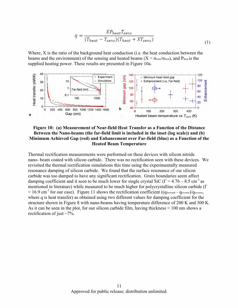
(1)
Where, X is the ratio of the background heat conduction (i.e. the heat conduction between the beams and the environment) of the sensing and heated beams (X = σsens/σheat), and Pheat is the supplied heating power. These results are presented in Figure 10a.
Figure 10: (a) Measurement of Near-field Heat Transfer as a Function of the Distance Between the Nano-beams (the far-field limit is included in the inset (log scale)) and (b)
Minimum Achieved Gap (red) and Enhancement over Far-field (blue) as a Function of the Heated Beam Temperature
Thermal rectification measurements were performed on these devices with silicon nitride nano- beam coated with silicon carbide. There was no rectification seen with these devices. We revisited the thermal rectification simulations this time using the experimentally measured resonance damping of silicon carbide. We found that the surface resonance of our silicon carbide was too damped to have any significant rectification. Grain boundaries seem affect damping coefficient and it seen to be much lower for single crystal SiC (Γ = 4.76 – 8.5 cm-1
as mentioned in literature) while measured to be much higher for polycrystalline silicon carbide (Γ = 16.9 cm-1
for our case). Figure 11 shows the rectification coefficient ((qforward – qreverse)/qreverse, where q is heat transfer) as obtained using two different values for damping coefficient for the structure shown in Figure 8 with nano-beams having temperature difference of 200 K and 300 K. As it can be seen in the plot, for our silicon carbide film, having thickness < 100 nm shows a rectification of just ~7%.

12 Approved for public release; distribution unlimited.
Figure 11: Normalized Rectification as a Function of Film Thickness for Measured Damping Coefficient of our Polycrystalline SiC (Γ = 9.5 cm-1)
As a comparison, the plot with lower damping coefficient (Γ = 9.5 cm-1) is also plotted, to show effect of reduced damping on rectification.
The design was revisited in the last part of the project to explore new materials that would fit our requirement of having lower resonance damping, narrower surface resonance, temperature dependent permittivity, better mechanical stability and offering higher operating temperatures. Currently, the known materials that have quite large temperature dependence is SiC, however our experimental data indicates that using polycrystalline SiC is not good for rectification due to its higher resonance damping. Other materials include VO2 which is incompatible with current fabrication processes and metals which had not been explored until now and are known to show temperature dependence [6]. Also to target a near field rectification which requires heat flow larger than n2 we need to use polar materials like SiO2, Si3N4, doped Si, Al2O3 etc., some of which have very little T-dependence (e.g. SiO2) and hence unsuitable for our application. Simulations were done to compute heat transfer between SiC and metal which showed considerable improvement in rectification. Some of the combinations that showed promising numbers of thermal rectification coefficient with thin metal film are SiC-Au (1.15), SiC-Pd (1.19), SiC-Ni (1.03), and SiC- Pt (0.92). However, it was found that part of heat transfer in these systems was due to non-resonance part of SiC at wavelengths where it is weakly lossy. This would require us to significantly modify our device dimensions to ensure total absorption of waves and hence heat transfer. A better approach to use Pt and SiO2 films where the magnitude of heat transfer is seen to be about 2 times higher than SiC and Pt. Also, it is found that magnitude of transfer power is higher for thinner metal films at resonance as compared to bulk metal (see Figure 12).
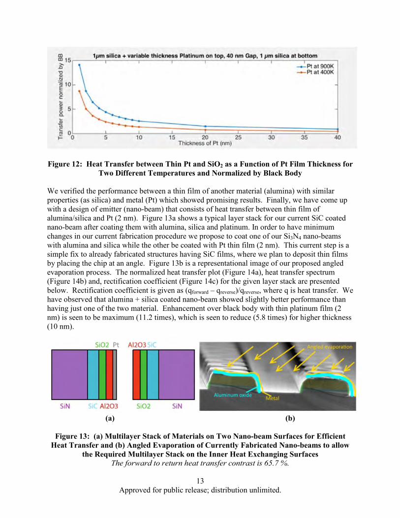
13 Approved for public release; distribution unlimited.
Figure 12: Heat Transfer between Thin Pt and SiO2 as a Function of Pt Film Thickness for
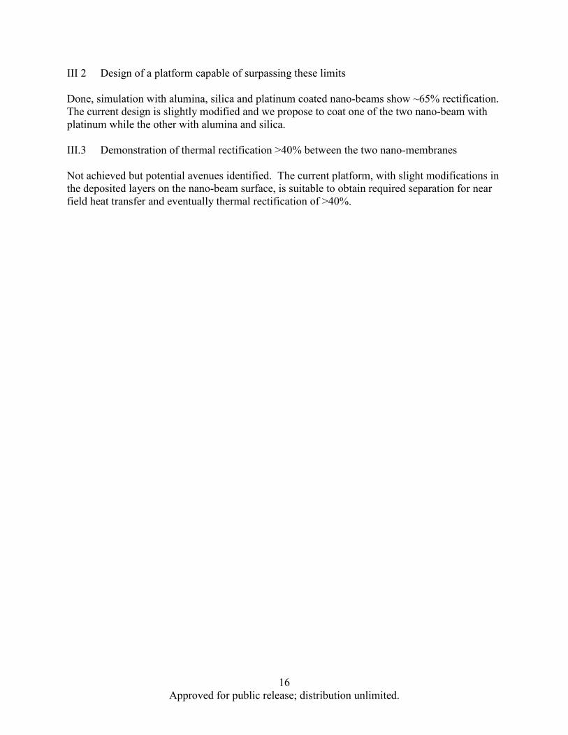
Two Different Temperatures and Normalized by Black Body We verified the performance between a thin film of another material (alumina) with similar properties (as silica) and metal (Pt) which showed promising results. Finally, we have come up with a design of emitter (nano-beam) that consists of heat transfer between thin film of alumina/silica and Pt (2 nm). Figure 13a shows a typical layer stack for our current SiC coated nano-beam after coating them with alumina, silica and platinum. In order to have minimum changes in our current fabrication procedure we propose to coat one of our Si3N4 nano-beams with alumina and silica while the other be coated with Pt thin film (2 nm). This current step is a simple fix to already fabricated structures having SiC films, where we plan to deposit thin films by placing the chip at an angle. Figure 13b is a representational image of our proposed angled evaporation process. The normalized heat transfer plot (Figure 14a), heat transfer spectrum (Figure 14b) and, rectification coefficient (Figure 14c) for the given layer stack are presented below. Rectification coefficient is given as (qforward – qreverse)/qreverse, where q is heat transfer. We have observed that alumina + silica coated nano-beam showed slightly better performance than having just one of the two material. Enhancement over black body with thin platinum film (2 nm) is seen to be maximum (11.2 times), which is seen to reduce (5.8 times) for higher thickness (10 nm).
(a) (b)
Figure 13: (a) Multilayer Stack of Materials on Two Nano-beam Surfaces for Efficient
Heat Transfer and (b) Angled Evaporation of Currently Fabricated Nano-beams to allow the Required Multilayer Stack on the Inner Heat Exchanging Surfaces
The forward to return heat transfer contrast is 65.7 %.

14 Approved for public release; distribution unlimited.
Figure 14: Heat Transfer Spectrum for the Structure Shown in Figure 12a
with 40nm Gap (a) Normalized heat transfer spectrum for two different temperatures, (b) Comparison of heat
transfer with black body, and (c) Forward to return heat transfer ratio.

15 Approved for public release; distribution unlimited.
3.0 Milestones Achieved During the Project
6 Months I.1 Design nano-membranes to exhibit thermal background conductance <200 nW/K Done, we have achieved 107 nW/K experimentally I.2 Fabricate nano-membranes Done, see experimental results I.3 Demonstrate background heat conduction of suspended nano-membranes <200 nW/K Done, we have achieved 107 nW/K experimentally I.4 Demonstration of suspended nano-membranes thermally isolated from the environment with <200 nW/K background conductance, and position controlled <20 nm precision Done, we achieved 10.5 nm precision positioning experimentally (see discussion related to Figure 5) 12 Months II.1 Demonstration of near-field heat transfer 20 times stronger than the far-field limit Done, 84X enhancement at low temperature and >20X for temperatures up to 725 K II.2 Determine the expected rectification dependence with gap between Silicon Carbide nano-beams Done, gap below 100 nm is needed to achieve >40% rectification together with milestone II.1 II.3 Optimize the thickness of a thin SiO2 coating one of the Silicon Carbide nano-beams to maximize rectification Done, 5 nm is the ideal thickness for 100 nm gap 18 Months III.1 Determine the fundamental limits to radiative rectification of the current platform based on the experimental results (Stanford) Done, no rectification was seen with the current platform due to high damping of resonance from SiC
16 Approved for public release; distribution unlimited.
III 2 Design of a platform capable of surpassing these limits Done, simulation with alumina, silica and platinum coated nano-beams show ~65% rectification. The current design is slightly modified and we propose to coat one of the two nano-beam with platinum while the other with alumina and silica. III.3 Demonstration of thermal rectification >40% between the two nano-membranes Not achieved but potential avenues identified. The current platform, with slight modifications in the deposited layers on the nano-beam surface, is suitable to obtain required separation for near field heat transfer and eventually thermal rectification of >40%.

17 Approved for public release; distribution unlimited.
4.0 References
[1] Lipson et al., CLEO: 2014 Post deadline Paper Digest, OSA Technical Digest (online), paper FTh5A.8. [2] Lipson et al., Nano Letters, v. 14, p. 6971 (2014). [3] Fan et al., J. Appl. Phys. 112, 024304 (2012). [4] Lipson et al., CLEO: 2015, OSA Technical Digest (online), paper FTh4E.1. [5] Lipson et al., arXiv:1509.08005 (2015). [6] Boltasseva et al., Adv. Mater., 25: 3264 (2013).

18 Approved for public release; distribution unlimited.
Appendix: Publications

19 Approved for public release; distribution unlimited.
FTh5A.8.pdf CLEO Postdeadline Papers © 2014 OSA
Demonstration of Strong Near-Field Radiative Heat
Transfer between Nanostructures Raphael St-Gelais,1 Biswajeet Guha,1 Linxiao Zhu,2 Shanhui Fan,2 and Michal Lipson*,1,3
1School of Electrical and Computer Engineering, Cornell University, Ithaca, New York 14853,
United States 2Ginzton Laboratory, Stanford University, Stanford, California 94305, United States
3Kavli Institute at Cornell for Nanoscience, Cornell University, Ithaca, New York 14853, United States * e-mail: [email protected]
Abstract: We demonstrate near-field radiative heat transfer between nanostructures and show that it dominates over other on-chip conduction channels. The measured heat transfer behavior matches the predictions of boundary element method simulations for parallel nanobeams. OCIS codes: (240.5420) Polaritons; (290.6815) Thermal Emission; (350.4238) Nanophotonics and photonic crystals.
Recently, there has been a growing interest in controlling radiative heat flow in the near-field [1], for applications in energy generation (e.g., thermophotovoltaics) and energy extraction (e.g., refrigeration mechanisms). Near-field heat transfer occurs when objects supporting surface phonon-polaritons (e.g., SiO2, SiC) or infrared plasmon-polaritons (e.g., doped silicon) are brought to submicron separation, such that their surface modes can evanescently couple and transfer heat with a magnitude that can significantly exceed the blackbody limit.
It has been shown theoretically that near-field thermal control can enable extreme functionalities including thermal transistors and thermal diodes, however these thermal elements would only be relevant to actual systems if shown to occur in integrated nanostructures with arbitrary geometries—where other conduction channels might dominate—rather than in semi-infinite or spherical geometries. To date, near-field radiative heat transfer has only been demonstrated using macroscopic objects (i.e., one or two semi-infinite surfaces [1-4] or a large probe tip approximated to a sphere [5]).
Here we demonstrate strong near-field radiative heat transfer between two integrated micromechanical nanostructures with novel geometries, and show that the heat transfer can be strong enough to dominate over other conduction channels, even on a fully integrated platform. The nanostructures are composed of two suspended SiO2 coated nanobeams (Fig. 1 a). The suspension mechanism is designed to minimize their background heat conduction, and to enable tuning of their separation distance using a microelectromechanical (MEMS) actuator (Fig. 1 b, c).
The structure is fabricated using chemical vapor deposition of the layers forming the beams, and e-beam
evaporation of the metals forming the heater, sensor and actuator. XeF2 etching is used to undercut the silicon substrate and release the structure. Si3N4 is used for mechanical purposes as its tensile residual stress (~ 950 MPa) allow for very long suspended structures [6] (200 µm for the two nanobeams and the four MEMS suspension springs). SiO2 is used for its previously demonstrated ability to support surface-phonon polaritons, and hence to allow near-field heat transfer. Al (250 nm) contacts are chosen to be thicker than the

20 Approved for public release; distribution unlimited.
Pt resistors (80 nm), such that the overall electrical resistance is dominated by Pt (~ 800 Ω). The fabricated structure is presented in Fig. 2.
Our results clearly indicate that, as the gap between the nanobeams reduces; near-field heat transfer
becomes dominant, overcoming any parasitic substrate conduction by more than a factor of four. During the experiment, constant heating current (1.67 × 10⁻⁴ A) and sensing current (10-6 A) are applied respectively to the fixed (heater) and mobile (sensor) beams. As the gap is tuned, changes of the electrical resistance of the Pt resistors are converted to temperature using a 0.0039 K-1 temperature coefficient of resistance for Pt. A separate experiment was also used to calibrate the temperature of the sensing beams for the initial 555 nm gap. The temperature of the heater beam relative to room temperature (∆Theater) was ramped from 0 to 100 K, while the temperature of the sensing beam (∆Tsensor) was measured. This calibration data was used to fix the initial values of ∆Tsensor = 2 K and ∆Theater = 75.5 K in Fig. 3 (a). One can see in Fig. 3 (a) that as the gap decreases from 555 nm to 100 nm, ∆Tsensor increases by more than a factor of four from 2 to 9 K. This strong gap dependence indicates that the heat conduction between the beams is dominated by near-field effects rather than parasitic background conduction (which are not gap dependent).
Fig. 2. (a) Scanning electron micrographs of a released device. (b) False color cross section of two nanobeams prior to substrate removal.
We show that in this novel geometry, the heat transfer is inversely proportional to the distance (d) between the nanobeams—which matches well with the 1/d1.68 exponential behavior predicted by boundary element method (BEM) simulations. Using conventional equivalent thermal circuit models and the background conductances of the fixed (400 nW/K) and mobile beam (235 nW/K), the heat transfer coefficient between the nanobeams (σ) is extracted from the heater temperature data of Fig. 3 (a). In Fig. 3 (b), this heat transfer coefficient is fitted to a σ = A/dα+C relation where A and C are the fit parameters and α = 1.68 is fixed. The constant C is included in the fit to account for background (Bgnd) heat conduction through the substrate and yields C = 4.0 nW/K. The α = 1.68 exponent is obtained by BEM simulations where the nanobeams cross sections can be approximated either as rectangles or as 250 nm radius cylinders with no noticeable difference (for gaps between 50 and 625 nm). The fit corresponds well with the experimental results considering a ± 15 nm uncertainty on the initial gap between the nanobeams (included as error bars in Fig 3 b).
Fig. 3. (a) Temperature (relative to room temperature ~ 293 K) of the mobile sensor beam (∆Tsensor) and the fixed heater beam (∆Theater) as a function of the gap between them. (b) Heat transfer coefficient between the nanobeams as a function of gap.
We presented the first demonstration of near-field radiative heat transfer between two nanoscale objects and showed that, even when integrated on the same chip, this heat transport mechanism can dominate over other heat conduction channels. We expect our results to have important implications in the development of practical applications of near-field heat transfer, such as thermal rectifiers and switches.

21 Approved for public release; distribution unlimited.
1. E. Rousseau, A. Siria, G. Jourdan, S. Volz, F. Comin, J. Chevrier, and J.-J. Greffet, "Radiative heat transfer at the nanoscale," Nat
Photon 3, 514-517 (2009). 2. A. Kittel, W. Müller-Hirsch, J. Parisi, S.-A. Biehs, D. Reddig, and M. Holthaus, "Near-field Heat transfer in a scanning thermal
microscope," Phys Rev Lett 95, 224301 (2005). 3. S. Shen, A. Narayanaswamy, and G. Chen, "Surface phonon polaritons mediated energy transfer between nanoscale gaps," Nano
Lett 9, 2909-2913 (2009). 4. R. S. Ottens, V. Quetschke, S. Wise, A. A. Alemi, R. Lundock, G. Mueller, D. H. Reitze, D. B. Tanner, and B. F. Whiting,
"Near-field radiative heat transfer between macroscopic planar surfaces," Phys Rev Lett 107, 014301 (2011). 5. B. Guha, C. Otey, C. B. Poitras, S. Fan, and M. Lipson, "Near-field radiative cooling of nanostructures," Nano Lett 12, 4546-4550 (2012). 6. M. Poot, and H. X. Tang, "Broadband nanoelectromechanical phase shifting of light on a chip," Appl Phys Lett 104, - (2014).

22 Approved for public release; distribution unlimited.
FTh4E.1.pdf CLEO:2015 © OSA 2015
Near-Field Radiative Heat Transfer between Integrated Nanostructures using Silicon Carbide
Raphael St-Gelais,1 Linxiao Zhu,2 Biswajeet Guha,1 Shanhui Fan,2 and Michal Lipson*,1,3
1School of Electrical and Computer Engineering, Cornell University, Ithaca, New York 14853, United States 2Ginzton Laboratory, Stanford University, Stanford, California 94305, United States
3Kavli Institute at Cornell for Nanoscience, Cornell University, Ithaca, New York 14853, United States * e-mail: [email protected]
Abstract: We present the first experimental demonstration near-field radiative heat transfer using silicon carbide. We achieve a 110× near-field enhancement, relative to the far-field limit, of the radiative heat transfer between integrated nanostructures. OCIS codes: (240.5420) Polaritons; (290.6815) Thermal Emission; (350.4238) Nanophotonics and photonic crystals.
Near-field radiative heat transfer recently attracted growing interest for applications such as thermal control [1, 2] and thermophotovoltaic energy generation [3, 4]. It occurs when objects supporting surface phonon-polaritons (e.g., SiO2, SiC) or infrared plasmon-polaritons are brought to submicron separation, such that their surface modes can evanescently couple. This coupling enables a radiative transfer of heat that can exceed the far-field blackbody limit by several orders of magnitude, while occurring over a relatively narrow frequency range.
To date, most experimental demonstrations of surface phonon mediated near-field heat-transfer relied on SiO2 as a material platform (e.g., [5-7]), which has limited potential applications due to its relatively broad and multi- frequency surface resonance spectrum. Silicon carbide, on the other hand, has a single narrowband surface resonance peak, which also present the advantage of varying dynamically as a function of temperature [1]. These features make SiC a material of choice for the design frequency tailored near-field thermal emitters [4, 8], and for thermal control devices such as thermal rectifiers [1].
Here we present the first experimental demonstration near-field radiative heat transfer using silicon carbide. We use plasma-deposited SiC to cover the side walls of two parallel nanobeams (see Fig 1 a). These nanobeams are integrated on a microelectromechanical (MEMS) platform (Fig. 1 b), similar to the one previously reported [7], that allow precise tuning of the distance between the nanobeams and measurement of the heat transfer. Platinum resistors on top of the beams are used both as resistive heaters and as temperature sensors. Si3N4 is used for mechanical purposes, as its tensile stress allow for long suspended nanostructures, while SiO2 is used solely as a protective coating for Si3N4 during structural release. The fabrication process of the device, except for deposition of silicon carbide, is the same as in [7].
Fig. 1. (a) False color cross-section view of the silicon carbide coated nanobeams prior to structural release. (b) Top view of structurally released
nanobeams integrated with the MEMS actuation mechanism. We characterize plasma deposited silicon carbide and predict a significantly narrower near-field heat transfer
spectrum than with the usual SiO2 material platforms. Amorphous SiC is deposited over the nanobeams by plasma enhanced chemical vapor deposition (PECVD) from SiH4 and CH4 gas precursors. It is then anisotropically etched, such that carbide is present only on the side walls of the nanobeams (see Fig. 1 a). The substrate is subsequently annealed at 1050 °C for 90 minutes to enable the formation of a microcrystalline SiC phase [9]. The mid-infrared permittivity of annealed SiC is extracted from the mid-infrared transmission spectrum at 70° grazing incidence of a

23 Approved for public release; distribution unlimited.
FTh4E.1.pdf CLEO:2015 © OSA 2015
120 nm thick film deposited on a blank silicon wafer. From this measurement, we find that the permittivity of the deposited material is described remarkably well by a Lorentz-Drude dispersion model, ε(ω) = ε∞ + ε∞(ωL
2 – ωT2) / (ωT
2 – ω2 – iΓω), with ωL = 955 cm-1, ωT = 790 cm-1, Γ = 17 cm-1, and ε∞ = 7.1. Using this permittivity we expect, in the general case of two parallel plates [10], a 4.5× narrower near-field heat transfer spectrum than using the permittivity of SiO2 [11]. We also expect narrower spectra for virtually any other geometry, although we have not yet investigated specific cases.
Our silicon carbide coating is found to enable strong near-field radiative heat transfer between two integrated nanobeams, showing a 110× near-field enhancement of heat transfer relative to the far-field limit. During the experiment, a constant 0.4 V heating voltage is applied to one of the nanobeams, while a constant 50 mV sensing voltage is applied to the other beam. The voltage across the MEMS actuators is then swept from 0 to 140 V to bring the two nanobeams closer together (see Fig. 2 a), while simultaneously measuring the nanobeams temperatures from the change of their electrical resistance [7]. The normalized radiative power transferred (Fig. 2 c) is then calculated from the measured nanobeam temperatures (Fig. 2 b). The gap values are obtained from the voltage applied on the MEMS actuator and by fitting the experimental heat transfer data to simulated values. These simulations are obtained by the Fourier modal method [7, 12], for a 145 K temperature difference between the beams. The simulated values are also fitted along the vertical axis to account for parasitic heat conduction through the substrate (~ 2 nW/K). The far-field limit is obtained by simulating the power radiated in the far-field by the silicon carbide surface of one of our nanobeam (0.79 nW/K), which is considered to be at ∆T = 185 K above room temperature.
Fig. 2. (a) Schematic representation of the experiment (not to scale). (b) Temperature, relative to ambient, of the heated (∆Thot) and the sensing
(∆Tcold) beams as a function of their separation distance (c) Normalized heat transfer power between two 200 µm long nanobeams as a function of their separation distance.
We showed that plasma-deposited SiC can enable strong near-field radiative heat transfer. We also achieved a
110× near-field enhancement of heat transfer, which is unprecedented for integrated nanostructures. These achievements should contribute to the development of thermal control [1] and thermo photovoltaic [4] devices.
1. C. R. Otey, W. T. Lau, and S. Fan, "Thermal Rectification through Vacuum," Phys Rev Lett 104, 154301 (2010). 2. P. Ben-Abdallah and S.-A. Biehs, "Near-Field Thermal Transistor," Phys Rev Lett 112, 044301 (2014). 3. S. Basu, Z. M. Zhang, and C. J. Fu, "Review of near-field thermal radiation and its application to energy conversion," Int J Energ Res
33, 1203-1232 (2009). 4. A. Narayanaswamy and G. Chen, "Surface modes for near field thermophotovoltaics," Applied Physics Letters 82, 3544-3546 (2003). 5. E. Rousseau, A. Siria, G. Jourdan, S. Volz, F. Comin, J. Chevrier, and J.-J. Greffet, "Radiative heat transfer at the nanoscale," Nat
Photon 3, 514-517 (2009). 6. S. Shen, A. Narayanaswamy, and G. Chen, "Surface phonon polaritons mediated energy transfer between nanoscale gaps," Nano Lett
9, 2909-2913 (2009). 7. R. St-Gelais, B. Guha, L. Zhu, S. Fan, and M. Lipson, "Demonstration of Strong Near-Field Radiative Heat Transfer between
Integrated Nanostructures," Nano Letters (2014). 8. M. Francoeur, M. Pinar Mengüç, and R. Vaillon, "Spectral tuning of near-field radiative heat flux between two thin silicon carbide
films," Journal of Physics D: Applied Physics 43, 075501 (2010). 9. L. Calcagno, P. Musumeci, F. Roccaforte, C. Bongiorno, and G. Foti, "Crystallization process of amorphous silicon–carbon alloys,"
Thin Solid Films 411, 298-302 (2002). 10. K. Joulain, J.-P. Mulet, F. Marquier, R. Carminati, and J.-J. Greffet, "Surface electromagnetic waves thermally excited: Radiative heat
transfer, coherence properties and Casimir forces revisited in the near field," Surface Science Reports 57, 59-112 (2005). 11. R. Kitamura, L. Pilon, and M. Jonasz, "Optical constants of silica glass from extreme ultraviolet to far infrared at near room
temperature," Appl. Opt. 46, 8118-8133 (2007). 12. C. R. Otey, L. Zhu, S. Sandhu, and S. Fan, "Fluctuational electrodynamics calculations of near-field heat transfer in non-planar
geometries: A brief overview," J Quant Spectrosc RA 132, 3-11 (2014).

24 Approved for public release; distribution unlimited.
Demonstration of Strong Near-Field Radiative Heat Transfer between Integrated Nanostructures Raphael St-Gelais,† Biswajeet Guha,† Linxiao Zhu,‡ Shanhui Fan,‡ and Michal Lipson*,†,§
†School of Electrical and Computer Engineering, Cornell University, Ithaca, New York 14853, United States ‡Ginzton Laboratory, Stanford University, Stanford, California 94305, United States §Kavli Institute at Cornell for Nanoscience, Cornell University, Ithaca, New York 14853, United States S Supporting Information
Recently there has been a growing interest in controlling radiative heat transfer in the near-field, 1-11 for applications in thermal miscroscopy, 12-14 thermophotovoltaic energy generation, 15-18 noncontact cooling, 19,20 and heat flow control. 21-28 Near-field heat transfer occurs when objects supporting surface phonon-polaritons (e.g., SiO2 and SiC) or infrared plasmon-polaritons (e.g., doped silicon) are brought to submicron separation, such that their surface modes can evanescently couple. This heat transfer occurs over a narrow frequency range (as opposed to the broadband nature of solid state conduction) and can exceed the blackbody limit by several orders of magnitude. It has been shown theoretically that near-field heat transfer can enable active functionalities such as thermal rectifiers, 21-23, 25-27 thermal transistors, 28 and thermal switches; 24 however, these devices would only be relevant to actual systems if shown to occur in integrated geometries, where unfortunately other conduction channels might dominate, rather than in macroscopic object. To date, near-field heat transfer has only been shown using macroscopic objects, i.e., one or two semi-infinite surfaces, 7,8,10-15,19 or a large probe tip approximated as a sphere. 20 Scaling up these macroscopic geometries to an actual thermal circuit composed of several components would be extremely challenging since even a single thermal transistor requires at least two near-field heat transfer junctions. On-chip integration is therefore necessary for the development of several applications. Moreover, miniaturization could eventually yield fundamental performance advantages over macroscopic experiments. For example,
nanopatterned objects can significantly relax the distance requirement for efficient near-field heat transfer between two objects, 9 while size-induced discretization of thermal modes could allow ultrahigh contrast rectification of heat transfer. 27 Here we show strong near-field radiative heat transfer in a novel on-chip geometrical configuration of two parallel suspended nanobeams where the distance between the beams can be tuned electrostatically. Our geometrical configuration is shown in Figure 1a. We use silicon dioxide (SiO2) for its surface phonon polariton resonances, at 495 and 1160 cm-1, shown to allow near-field heat transfer. 7,8,11,20 Silicon nitride (Si3N4) is used solely for mechanical purposes as its tensile residual stress (~950 MPA) allows for long suspended nanobeams that are thermally isolated from the substrate. We use platinum (Pt) resistors both as resistive heaters and as thermometers to measure the amount of heat transfer. The gap between the two nanobeams is tuned using a monolithically integrated microelectromechanical (MEMS) actuator (see Figure 2a). Electrostatic actuation is chosen for its negligible power consumption and hence negligible parasitic heat generation. When an actuation voltage is applied, the electric field across the two actuation capacitors induces an attraction force that brings the suspended part of the actuator closer to the fixed heated beam (see Figure 2b). The design of the MEMS, in particular the use of deposited metal electrodes over a nitride mechanical platform, was inspired in part by ref Received: August 22, 2014 Revised: October 30, 2014 Published: November 24, 2014
Letter
pubs.acs.org/NanoLett
ABSTRACT: Near-field heat transfer recently attracted growing interest but was demonstrated experimentally only in macro- scopic systems. However, several projected applications would be relevant mostly in integrated nanostructures. Here we demon- strate a platform for near-field heat transfer on-chip and show that it can be the dominant thermal transport mechanism between integrated nanostructures, overcoming background substrateconduction and the far-field limit (by factors 8 and 7,respectively). Our approach could enable the development of active thermal control devices such as thermal rectifiers and transistors.
S

25 Approved for public release; distribution unlimited.
Figure 1. (a) Schematic representation of the experiment. At small gap, evanescent surface polariton resonances at the SiO2 surfaces couple to enable near-field radiative heat transfer between the nanobeams. Si3N4 is used for mechanical purposes, while Pt is used both as a resistive heater and a temperature sensor. (b) Theoretical prediction of the heat transfer between two nanobeams of 200 μm length and 500 nm × 1.1 μm cross-section. The SiO2 thickness in this case is 100 nm.
Figure 2. (a) Schematic (not to scale) and electrical circuit of the two- nanobeam system integrated with the MEMS actuator. (b) Schematic (not to scale) of the MEMS displacement. (c) Scanning electron micrographs (SEM) of the device. (d) False color SEM of the nanobeam cross section prior to substrate removal.
29. To tune the gap continuously while avoiding electrostatic pull-in effect, the gap between the electrodes of the actuation capacitors (3 μm) is designed to be more than three times larger than the maximum possible displacement (given by the gap between the nanobeams, designed to be 700 nm). The length of the fixed beam, the mobile sensing beam, and each of the four MEMS suspension springs is 200 μm. Such large dimensions are required to minimize the mechanical stiffness of the suspension springs and hence to allow full range displacement with an actuation voltage below 200 V. These large dimensions are also beneficial to the thermal isolation of the nanobeams (i.e., to the minimization of the background thermal heat conduction between the nanobeams and the substrate). The simulated heat transfer power between the nanobeams presents a drastic enhancement of heat transfer in the near-field (see Figure 1b). The near-field simulation in Figure 1b is performed using a Fourier modal method based on the fluctuational electrodynamics formalism,30,31 considering beams of 200 μm length and 500 nm × 1.1 μm cross section (including a 100 nm thick SiO2 coating). The temperature difference between the nanobeams is 130 K (as in our experimental results), with the mobile sensing beam maintained at room temperature. Repeating the near-field simulation while replacing the Si3N4 core with SiO2 shows that the Si3N4 core has a negligible effect on the heat transfer compared with a beam that would be made entirely of SiO2. The insensitivity of heat transfer to the core material results from the surface wave nature of the SiO2 surface phonon-polariton that dominates heat transfer at small gaps. In the gap range of Figure 1b, the heat transfer power approximately scales as 1/gap1.68. At much smaller distances (i.e., distances much smaller than the beam dimensions), we expect the heat transfer to be proportional to 1/gap2, as for parallel plates.19 The far-field value in Figure 1b is the total far-field emission, integrated over all directions and all frequencies, for a nanobeam maintained at 130 K above room temperature. This value is calculated by the Fourier modal analysis method for a periodic array of nanobeams with a periodicity much larger than the size of nanobeams, such that they do not interact with each other. The structure is fabricated using conventional nano- fabrication processes, which consist of low pressure chemical vapor deposition (LPCVD) of SiO2 and Si3N4, and electron- beam evaporation of platinum resistors and aluminum electrical contacts. The fabrication process begins with the successive deposition of 100 nm of SiO2, 300 nm of Si3N4, and 100 nm of SiO2 on a virgin silicon wafer. The MEMS and nanobeams are then defined by deep ultraviolet lithography and etched in CHF3 + O2 chemistry using an inductively coupled plasma reactive ion etching (ICP-RIE) reactor. Following this etch step, a third layer of SiO2 is deposited, again by LPCVD, in order to conformally cover the sidewalls of the etched structures. This layer is then anisotropically etched (using the same ICP-RIE chemistry) to clear the bottom of the

26 Approved for public release; distribution unlimited.
trenches for subsequent isotropic release, while leaving some SiO2 on the sidewalls of the nanobeams (see the final nanobeams cross section in Figure 2d). Platinum and aluminum are then successively deposited over the defined structure by electron beam evaporation and lift-off. The aluminum layer is chosen to be much thicker (250 nm) than the platinum layer (60 nm), such that the resistance of the aluminum contacts is negligible compared with the platinum resistors. The higher electrical conductivity of aluminum, relative to platinum, also contributes to make the resistance of the aluminum contacts negligible. The structure is finally released in XeF2 gas isotropic etching of silicon. Release holes are included on the larger parts of the MEMS (see Figure 2c) to facilitate the isotropic release step. The fabricated MEMS platform is found to allow precise control of the nanobeam displacement over 500 nm with ±10 nm accuracy. The displacement of the MEMS actuator as a function of the applied voltage is measured using a custom- made image processing algorithm coupled with optical microscopy. Optical images of the MEMS are taken at a 50× magnification (see Figure 3a) for different actuation voltages.
Figure 3. (a) Optical images of the MEMS displacement at actuation voltages of 0 (left) and 116 V (right). The images are treated by our image processing algorithm to extract the MEMS displacement. (b) Measured MEMS displacement as a function of the actuation voltage. The cubic spline interpolation is used to convert actuation voltages to displacement values. The relative position of the two beams is then extracted by fitting Gaussian distributions over the nanobeam images. This fitting algorithm is repeated and averaged over all cross-section slices of each image file (i.e., over each vertical slice of the nanobeams in Figure 3a). The measured displacement of the mobile nanobeam is presented in Figure 3b, which shows smooth and continuous control of the MEMS position as a function of the applied voltage. The uncertainty on the measured displacement arises from the precision of the image processing algorithm (±5.5 nm) and from the uncertainty on the scale of the image (67.8 ± 0.7 nm/pixel). The detailed calculation of these uncertainty values is presented in Supporting Information S1. It should be
noted that, although we can measure the relative displacement of the MEMS with great accuracy, our knowledge of the absolute distance between the two nanobeams suffers from greater uncertainty due to our difficulty in evaluating the initial beam separation distance (d0 = 740 nm). Although d0 is fixed by design, it changes significantly upon release due to internal material stress and must therefore be evaluated from scanning electron micrographs of the released device. We also note that the maximum achieved displacement in Figure 3b is slightly below 500 nm, while the initial gap is around 740 nm, which means that the minimum achievable gap is in the 200−250 nm range. The reason why the gap cannot be reduced further is not fundamental and is detailed in Supporting Information S2. Measurements of temperature changes as a function of nanobeam separation clearly indicate that near-field heat transfer is the dominant thermal transport mechanism between the nanobeams. All heat transfer experiments are carried in vacuum at a pressure of 1.5 × 10⁻⁴ Torr. The electrical measurements are performed using an Agilent B1500A semiconductor device parameter analyzer. In the heat transfer experiment, the gap between the nanobeams is progressively reduced using the MEMS actuator, while a constant voltage of Vfix = 0.22 V is supplied to heat up the fixed nanobeam (which translates to 33 μW of electrical power at the initial beam separation). Meanwhile, the temperature of the mobile sensing beam is measured using a 10 μA sensing current (which translates to 0.12 μW electrical power, more than 2 orders of magnitude lower than the heating power applied to the fixed beam). To ensure that the system is in its steady state at each measurement point, a 0.2 s delay is included between the MEMS actuation voltage setting and the temperature readout. This delay is orders of magnitude larger than the thermal time constants of the fixed heated beam (1.3 ms) and the mobile sensing beam (7.4 ms). Those time constants were measured in a separated experiment by applying a step voltage variation to the nanobeam resistors while measuring their transient current. The temperatures of both nanobeams are calculated from the measured electrical resistance (R) of their platinum resistors, which changes as ΔR/R = TCR × ΔT, where the temperature coefficient of resistance (TCR) is 0.00181 K-1. The TCR value was calibrated separately by measuring the resistance of a device placed on a hot plate ramped from 20 to 150 °C. The temperature (relative to room temperature) of both the fixed heated beam and the mobile sensing beam, as a function of their separation distance, is presented in Figure 4. As the gap decreases, the temperature of the fixed heated beam diminishes slightly as it loses heat to the mobile beam. More importantly, the temperature of the mobile sensing beam increases by almost a factor of 5 (from Tmob = 3 K to Tmob = 14.7 K). Such increase is a clear indication that as the gap decreases, near-field effects, rather than conduction through the substrate, dominate heat transfer between the nanobeams (substrate conduction should indeed be gap independent).

27 Approved for public release; distribution unlimited.
Figure 4. Measured temperature (relative to room temperature) of the fixed heated beam (Tfix) and the mobile sensing beam (Tmob) as a function of their separation distance. In this case, a constant heating voltage is supplied to the fixed beam, while only a sensing current is supplied to the mobile beam. The near-field heat transfer power is extracted from our temperature measurements and is found to be 8 times stronger than substrate conduction and 7 times stronger than the far- field radiation limit. We can convert the temperature data of Figure 4 to heat transfer power values (q) using eq 1, which is obtained by solving the equivalent thermal circuit of the experiment (as is routinely done for on-chip thermal transport experiments32).
In eq 1, q is the power transfer (in Watt/K) normalized by the temperature difference between the beams, Tfix and Tmob are, respectively, the temperature of the fixed heated beam and the mobile sensing beam, and X = σmob/σfix is the ratio of the background heat conductions of the nanobeams. For each nanobeam, the background heat conduction between the beam and the substrate (i.e., σmob and σfix) is determined by applying a ramping electrical power to the beam while simultaneously measuring its temperature (i.e., its electrical resistance). The inverse of the slope of this temperature vs electrical power measurement yields the background conduction, in units of Watt/K. We obtain conduction values of σfix = 237 nW/K and σmob = 107 nW/K for the fixed heated beam and the mobile sensing beam, respectively. Using these values and the temperature data of Figure 4, we obtain the heat transfer power as a function of the nanobeam separation (see Figure 5). In Figure 5, the horizontal error bars correspond to the error on the measurement of the MEMS displacement (see Figure 3). Vertical error bars are not visible, as they are determined by the very high resolution of the Agilent device parameter analyzer. The theory curve is the same as in Figure 1, but is now translated horizontally and vertically to best fit the experimental data. The horizontal translation is included to account from our uncertainty on the initial distance (d0) between the beams (see discussion related to Figure 3 and the MEMS displacement measurement), while the vertical translation accounts for spurious conduction of heat through the substrate. The translation that best fits the experimental data is +49 nm horizontally and +1.49
nW/K vertically. After fitting, the theory is found to correspond closely with the experimental data. Slight discrepancies between theory and measurements most likely arise from deviation of the beam cross-section from the perfectly rectangular shape considered in the simulations (see Figure 2d). The 1.49 nW/K susbtrate conduction obtained from the fit is included in Figure 5, from which we note that spurious substrate conduction account for less than 12% of the total heat transfer at the smallest gap. The far-field radiation limit (1.7 nW/K) is also included in Figure 5 in order to illustrate the strong enhancement of heat transfer in the near- field compared to the far-field value. The far-field emission is obtained by the same Fourier modal method used in Figure 1.
Figure 5. Heat transfer power between the nanobeams as a function of their separation distance. Substrate conduction is found to account for less than 15% of the total heat transfer at the smallest gap. Near-field heat transfer is also found to be 7 times stronger than the far-field limit (1.7 nW/K above the substrate conduction, for the current geometry and temperatures). We have presented the first demonstration of near-field radiative heat transfer between two integrated nanostructures and shown that near-field radiation can be the dominant heat transport channel between these structures, even on a fully integrated platform. The approach, based on nanobeam integration with MEMS actuation, could enable the development of new near-field thermal control devices, such as thermal rectifiers and thermal transistors. ASSOCIATED CONTENT Supporting Information (1) Uncertainty on the MEMS displacement measurement. (2) Discussion on the minimum achievable nanobeam separation. (3) Supplemental calibration of the temperature measurement. This material is available free of charge via the Internet at http://pubs.acs.org. AUTHOR INFORMATION Corresponding Author *E-mail: [email protected]. Notes The authors declare no competing financial interest.

28 Approved for public release; distribution unlimited.
ACKNOWLEDGMENTS The authors gratefully acknowledge Clayton Otey for using some of his codes for the calibrations of the numerical simulations presented here. The authors gratefully acknowledge support from DARPA for award FA8650-14-1-7406 supervised by Dr. Avram Bar-Cohen. This work made use of the Cornell Center for Materials Research Shared Facilities, which are supported through the NSF MRSEC program (DMR- 1120296), and of the Cornell NanoScale Facility, a member of the National Nanotechnology Infrastructure Network, which is supported by the National Science Foundation (Grant ECCS-0335765). R.S.-G. holds a postdoctoral fellowship from the Fonds de recherche du Quebec−Nature et Technologies. REFERENCES (1) Polder, D.; Van Hove, M. Phys. Rev. B 1971, 4 (10), 3303−3314. (2) Loomis, J. J.; Maris, H. J. Phys. Rev. B 1994, 50 (24), 18517−18524. (3) Pendry, J. B. J. Phys.: Condens. Matter 1999, 11 (35), 6621. (4) Fu, C. J.; Zhang, Z. M. Int. J. Heat Mass Transfer 2006, 49 (9− 10), 1703−1718. (5) Volokitin, A. I.; Persson, B. N. J. Rev. Mod. Phys. 2007, 79 (4), 1291−1329. (6) Francoeur, M.; Mengüc, M. P.; Vaillon, R. Appl. Phys. Lett. 2008, 93 (4), 043109. (7) Rousseau, E.; Siria, A.; Jourdan, G.; Volz, S.; Comin, F.; Chevrier, J.; Greffet, J.-J. Nat. Photon. 2009, 3 (9), 514−517. (8) Shen, S.; Narayanaswamy, A.; Chen, G. Nano Lett. 2009, 9 (8), 2909−2913. (9) Rodriguez, A. W.; Ilic, O.; Bermel, P.; Celanovic, I.; Joannopoulos, J. D.; Soljacic, 2011, 107 (11), 114302. M.; Johnson, S. G. Phys. Rev. Lett. 2011, 107 (11), 114302. (10) Kralik, T.; Hanzelka, P.; Zobac, M.; Musilova, V.; Fort, T.;Horak, M. Phys. Rev. Lett. 2012, 109 (22), 224302. (11) Shi, J.; Li, P.; Liu, B.; Shen, S. Appl. Phys. Lett. 2013, 102 (18), 183114. (12) Kittel, A.; Müller-Hirsch, W.; Parisi, J.; Biehs, S.-A.; Reddig, D.; Holthaus, M. Phys. Rev. Lett. 2005, 95 (22), 224301. (13) De Wilde, Y.; Formanek, F.; Carminati, R.; Gralak, B.; Lemoine, P.-A.; Joulain, K.; Mulet, J.-P.; Chen, Y.; Greffet, J.-J. Nature 2006, 444 (7120), 740−743. (14) Jones, A. C.; Raschke, M. B. Nano Lett. 2012, 12 (3), 1475−1481. (15) DiMatteo, R. S.; Greiff, P.; Finberg, S. L.; Young-Waithe, K. A.; Choy, H. K. H.; Masaki, M. M.; Fonstad, C. G. Appl. Phys. Lett. 2001, 79 (12), 1894−1896. (16) DiMatteo, R.; Greiff, P.; Seltzer, D.; Meulenberg, D.; Brown, E.;Carlen, E.; Kaiser, K.; Finberg, S.; Nguyen, H.; Azarkevich, J. In Micron-gap Thermophotovoltaics (MTPV), Sixth Conference on
Thermophotovoltaic Generation of Electricity: TPV6; AIP Publishing: Melville, NY, 2004; pp 42−51. (17) Laroche, M.; Carminati, R.; Greffet, J.-J. J. Appl. Phys. 2006, 100 (6), 063704. (18) Basu, S.; Zhang, Z. M.; Fu, C. J. Int. J. Energy Res. 2009, 33 (13), 1203−1232. (19) Ottens, R. S.; Quetschke, V.; Wise, S.; Alemi, A. A.; Lundock, R.; Mueller, G.; Reitze, D. H.; Tanner, D. B.; Whiting, B. F. Phys. Rev. Lett. 2011, 107 (1), 014301. (20) Guha, B.; Otey, C.; Poitras, C. B.; Fan, S.; Lipson, M. Nano Lett. 2012, 12 (9), 4546−4550. (21) Otey, C. R.; Lau, W. T.; Fan, S. Phys. Rev. Lett. 2010, 104 (15), 154301. (22) Basu, S.; Francoeur, M. Appl. Phys. Lett. 2011, 98 (11), 113106. (23) Iizuka, H.; Fan, S. J. Appl. Phys. 2012, 112 (2), 024304. (24) Zhu, L.; Otey, C. R.; Fan, S. Appl. Phys. Lett. 2012, 100 (4), 044104. (25) Wang, L. P.; Zhang, Z. M. Nanoscale Microscale Thermophys. Eng. 2013, 17 (4), 337−348. (26) Park, K.; Zhang, Z. Front. Heat Mass Transfer 2013, 4 (1), 013001. (27) Zhu, L.; Otey, C. R.; Fan, S. Phys. Rev. B 2013, 88 (18), 184301. (28) Ben-Abdallah, P.; Biehs, S.-A. Phys. Rev. Lett. 2014, 112 (4), 044301. (29) Poot, M.; Tang, H. X. Appl. Phys. Lett. 2014, 104 (6), 061101. (30) Lussange, J.; Guerout, R.; Rosa, F. S. S.; Greffet, J. J.; Lambrecht, A.; Reynaud, S. Phys. Rev. B 2012, 86 (8), 085432. (31) Otey, C. R.; Zhu, L.; Sandhu, S.; Fan, S. J. Quant. Spectrosc. Radiat. Transfer 2014, 132 (0), 3−11. (32) Chang, C. W.; Okawa, D.; Majumdar, A.; Zettl, A. Science 2006, 314 (5802), 1121−1124.

29 Approved for public release; distribution unlimited.
,
Near-field radiative heat transfer between nanostructures in the deep sub-wavelength regime
Raphael St-Gelais,1,2 Linxiao Zhu,3 Shanhui Fan,3 and Michal Lipson*,1,2
1School of Electrical and Computer Engineering, Cornell University, Ithaca, New York 14853, United States 2Department of Electrical Engineering, Columbia University, New York, New York 10027, United States
3Ginzton Laboratory, Stanford University, Stanford, California 94305, United States * e-mail: [email protected]
Introductory paragraph Radiative heat transfer between parallel objects separated by deep sub-wavelength distances and subject to large thermal gradients (>100 K) could enable breakthrough technologies for electricity generation1-5 and thermal transport control6-8. However, thermal transport in this regime has never been achieved experimentally due to the difficulty of maintaining large thermal gradients over nm-scale distances while avoiding other heat transfer mechanism such as conduction. Previous experimental measurement between parallel planes 1,9-13 were limited to distances greater than 500 nm11 (with a 20 K thermal gradient), which is much larger than the theoretically predicted distance (<100 nm) required for most applications1-8. Here we show near- field radiative heat transfer between parallel nanostructures in the deep sub-wavelength regime using high precision micro electromechanical (MEMS) displacement control. We also exploit the high mechanical stability of structures under high tensile stress to minimize thermal buckling effects and maintain small separations at large thermal gradients. We achieve an enhancement of heat transfer of almost two orders of magnitude relative to the far-field limit, which corresponds to a 54 nm separation. We also achieve a high temperature gradient (260 K) between the cold and hot surfaces while maintaining a ~100 nm distance. Main text Radiative heat transfer between objects separated by deep sub-wavelength distances can exceed the conventional laws of thermal radiation14,15, while being concentrated over a quasi- monochromatic frequency range16. This heat transfer occurs through evanescent coupling of thermally excited surface resonances, and consequently scales inversely with separation (as 1/dα where α is a geometry dependent factor). The separation (d) at which this regime occurs depends on the geometry of the system and on the materials involved, but it is generally around 200 nm for identical parallel structures relying on surface phonon resonances17. For applications such as electricity generation and thermal control, the two materials involved are non-identical, such that resonant coupling is less efficient and separations <100 nm are typically required3,18. The unique features of heat transfer in the deep sub-wavelength regime (i.e., large magnitude and quasi-monochromatic spectral distribution) could allow high efficiency generation of electricity from heat1,3-5 and novel thermal control devices6,8. For example, near-field heat transfer between a hot thermal emitter and a cold photovoltaic cell could allow energy generation with a greater efficiency (>30% for a T = 600 K heat source5) than using either thermoelectric generator or single junction solar photovoltaic cells. It is also predicted that engineering the surface resonance frequencies of parallel structures could allow novel thermal control devices such as thermal rectifiers6,7 or thermal transistors8.

30 Approved for public release; distribution unlimited.
OO w2 -w2-irw
These applications rely on radiative heat transfer between parallel structures in the deep sub- wavelength regime, and on a high temperature gradient between them, neither of which have been achieved experimentally. Near-field enhancement of heat transfer was demonstrated between parallel plates using active parallelism control10,12,13, or mechanical spacers1,9,11. The smallest separation achieved in these experiments is 500 nm11 (with a 20 K thermal gradient), which is small enough to overcome the far-field blackbody radiation limit, but not enough to reach the deep sub-wavelength regime where the heat flux is effectively concentrated around a single frequency17. Furthermore, the highest temperature gradient (∆T) achieved in these experiments is 85 K9 (for a 1.6 µm separation), which is relatively small, especially for energy generation applications where the generated power and the efficiency (η) both scale with the temperature gradient (e.g., ηCarnot = ∆T/Thot). In sphere-plane geometries19-21, distances as low as 20 nm21 were achieved, which is close to the distance where the deep sub-wavelength regime occurs (typically 10-20 nm)20. However, this configuration allows near-field heat transfer only over a small area at the tip of the sphere, and is hence not practical for energy generation applications where the power is proportional to the area. Here we show radiative heat transfer in the deep sub-wavelength regime between two parallel structures using precise positioning with integrated microelectromechanical actuators (MEMS). Our system relies on parallel nanobeams monolithically integrated with electrostatic comb drive actuators (Fig. 1). These actuators allow precise displacement control, limited in theory to sub- nm precision by Brownian motion and by actuation voltage uncertainty (see supplementary information S3). Their power consumption is also low (<30 pW in the ON state), more than three orders of magnitude lower than the typical heating power applied to the system. We rely on the surface phonon-polariton resonance of SiC to create the surface waves responsible for near field heat transfer. Note that although there has been a lot of theory work on near-field heat transfer with thin SiC films2,6,22-24, no experimental work has been reported. We use silicon carbide deposited by plasma enhanced chemical vapor deposition (PECVD) and annealed to create a microcrystalline (µ-SiC) phase (see methods). We characterize the infrared permittivity (ε) of µ-SiC for the first time and find it to be well described by a Lorentz-Drude relation (equation 1) that has a sharper infrared resonance than most commonly used SiO2:
E(w) = E (1 + wL-wT ), (1)
T
with ωT = 789 cm-1, ωL = 956 cm-1, ε ∞ = 8, Γ = 20 cm-1 (see characterization and extended discussion in supplementary information S1.)
We simulate the heat transfer between the nanobeams using a Fourier modal method based on the fluctuational electrodynamics formalism25,26 and we predict that the deep sub-wavelength regime occurs at distances <200 nm. The exact geometry of the nanobeams considered for this simulation is presented in supplementary information S2. For distances smaller than 200 nm (see Fig 1 b) the simulated results follow the typical 1/dα law that is characteristic of the deep sub- wavelength regime. The geometry dependent factor α = 1.75 in this case is intermediate between the parallel plate case (α = 2) and the sphere-plane case (α = 1.5). The simulations also show that heat transfer in the deep sub-wavelength regime is quasi-monochromatic (see Fig 1 c) and centered around the ε(ω) = -1 surface phonon resonance frequency of SiC (937 cm-1).

31 Approved for public release; distribution unlimited.
Figure 1 (a) Schematic of the device geometry (not to scale) and operation principle. (b) Simulated radiative heat transfer between two nanobeams as a function of the distance. The hot beam is set at T = 10 K above room temperature. The deep sub-wavelength regime occurs for beam separation below 200 nm, where the heat transfer begin to scale as 1/d1.75 (c) Simulated heat transfer spectrum between the nanobeams at two different separation. For d = 50 nm, the heat transfer is concentrated mainly around the SiC surface resonance (near ω = 937 cm-1). The secondary peak (at ω = 844 cm-1) results from a contribution of Si3N4 to the heat transfer. (d) False color scanning electron micrograph (SEM) of the device after structural release. (e) SEM false color cross section view of the nanobeams prior to structural release. In order to achieve experimentally very small distances over large areas, it is critical that the two surfaces are completely parallel. Therefore no buckling should occur under changes of temperature. We prevent buckling by designing the beams such that they preserve the high tensile stress of silicon nitride (~900 MPa) after structural release (see Fig. 1 a). This stress prevents thermal bimorph effect from causing buckling that would catastrophically impact the minimum achievable distance in our system at high temperatures (see Fig. 2). Our design also suppresses stress induced deformation that prevented us from reaching the deep sub-wavelength regime with our previous platform27.

32 Approved for public release; distribution unlimited.
Figure 2 (a) Schematic of nanobeam buckling due to thermal bimorph effect. (b) Simulated buckling of a doubly clamped, 600 µm long, bi-material beam made of Si3N4 (300 nm thick) and Pt (50 nm thick). In order to measure the heat transfer, the beams are brought together by sweeping the voltage supplied to the MEMS actuator (see VMEMS in Fig. 1 a) while the temperature of the heated beam (Theat) and the sensing beam (Tsens) are measured (see Methods). The result of this scan is presented in Fig. 3 (b), where the inset shows the transition between near-field and contact regimes. The displacement of the nanobeams as a function of the MEMS voltage is also measured in a separate experiment (supplementary information S3) and presented in Fig 3 (a). The experimental data of Fig 3 is converted to normalized heat transfer power (q, in W/K) using
(2) where (X = σsens/σheat) is the ratio of the background heat conduction (σ) of the two nanobeams, and Pheat is the supplied heating power. From the symmetry of the system, X ≈ 1 for scans of relatively low temperature amplitude such as in Fig 3 (b).

33 Approved for public release; distribution unlimited.
Figure 3 (a) Measured and fitted displacement of the nanobeams as a function of the voltage on the MEMS actuator. (b) Temperature of the heated beam (Theat) and the sensing beam (Tsens) as a function of the voltage on the MEMS actuator.
The measured heat transfer agrees well with the simulated values. In Fig 4 (a), the experimental heat transfer power is plotted and compared with the simulated data (which is fitted vertically and horizontally, see methods). At gaps larger than ∼150 nm, the experimental values are slightly larger than the simulated ones. This could be caused by larger infrared material absorption coefficient (of, e.g., Si3N4) than considered in the simulations, which would increase the contribution of propagating wave to the heat transfer. This increase causes the deep sub- wavelength regime to occur at <150 nm distances, rather than <200 nm in the simulated data (Fig 1 b). At gaps smaller than 150 nm, the experimental data matches the simulation more closely, and small deviations between simulation and experiments are visible only in the logarithmic scale inset in Fig. 4 (a). These are likely caused by the inability of the polynomial fit to perfectly match the experimental MEMS displacement in Fig 3 (a), or by slightly different experimental conditions between the MEMS displacement measurement (supplementary information S3) and the heat transfer measurement.

34 Approved for public release; distribution unlimited.
Figure 4 (a) Measured and simulated heat transfer between the nanobeams as a function of separation. The inset shows the same result, in logarithmic scale. (b) Minimum gap (i.e., before the beam come into contact) and maximum enhancement (relative to the far-field limit) achieved as a function of the heated beam temperature. This figure shows our ability to maintain the beam separation in the deep sub-wavelength regime (gap < 150 nm) for beam temperatures as high as 720 K. The error bars are calculated from the uncertainty on the thermal coefficient of resistance and the effective beam interaction length (see supplementary information S2). (c) Near-field heat transfer intensity (power per unit area) as a function of the temperature of the heated beam. The area is taken as the inner SiC surface of the nanobeams. We achieve an 82× enhancement of heat transfer over the far-field limit and are able to maintain the nanobeams in the deep sub-wavelength regime for temperature gradients as high as 260 K. The highest heat transfer value achieved in Fig 4 (a) is 34 nW/K, which is 82× larger than the beam far-field radiation limit (0.42 nW/K). We define this limit as the maximum power that the SiC surface of the nanobeam can radiate to the far-field, at a given temperature (see Methods). This enhancement corresponds to a 54 nm gap between the nanobeams, which is well within the deep sub-wavelength regime (<150 nm). The measurement of Fig 4 (a) is repeated for different temperatures of the heated beam. In Fig 4 (b), the minimum achieved gap (i.e. the smallest near- field gap achieved before the beams come into contact with each other) is reported as a function of the heated beam temperature. The minimum achieved near-field gap is found to increase slightly

35 Approved for public release; distribution unlimited.
with temperature. This is most likely due to thermal buckling that occurs despite the large stiffness of the nanobeams. The increase is indeed consistent with the simulated buckling presented in Fig 2. We reach the deep sub-wavelength regime (i.e. distance <150 nm) with heated beam temperatures as high as 720 K (i.e. 425 K above room temperature). In this case the temperature gradient between the beams is 260 K (see supplementary information S4). Such high thermal gradient translates to a high (>6 W/cm2
, see Fig 4 c) net energy flux which, for applications such as energy generation, is often more crucial than the relative enhancement itself.
We achieved the first demonstration of near-field radiative heat transfer between parallel objects in the deep sub-wavelength regime and at high temperature gradient. This nanoscale approach offers a clear path towards applications of near-field heat transfer such as near-field thermophotovolatic energy generation. We also note that our approach could be scaled up to a larger effective area by simply arraying several nanobeams (atop, e.g., a photovoltaic cell) and by individually controlling their out-of-plane displacement using MEMS actuators. Methods Microcrystalline Silicon Carbide (µ-SiC) deposition Amorphous silicon carbide is first deposited in by plasma enhanced chemical vapor deposition (PECVD) from silane (SiH4) and methane (CH4) gas precursors in a 1:20 ratio and with argon as a dilution gas. The film is then annealed in argon atmosphere at 1100 °C for 90 minutes to grow a microcrystalline phase28. The silane/methane concentration ratio was optimized by measuring the refractive index of the film by ellipsometry after the anneal process. The 1:20 ratio yields a 2.53 refractive index (at λ = 1500 nm), which is very close to the theoretical value (2.57). Higher or lower ratio both lead to higher refractive index, which is consistent with the growth of silicon or carbon clusters during annealing of non-stoichiometric films. Device fabrication A SiO2/Si3N4/SiO2 film stack is first deposited on a conventional silicon wafer by low pressure chemical vapor deposition (LPCVD). The structure is then defined by deep-UV lithography and anisotropically etched in fluorine chemistry. SiC is then deposited over the structure by PECVD an annealed at 1100 °C to grow the µ-SiC phase. SiC is anisotropically etched in fluorine chemistry, such that µ-SiC remains only on the nanobeam sidewalls. Platinum heaters and metal contact are deposited be electron beam evaporation and lift-off using a chrome adhesion layer. The device is finally released by undercutting the silicon substrate in XeF2 chemistry. Experimental condition & procedure The heat transfer experiments are performed at room temperature in a high vacuum (9 ×10⁻⁵ torr) electrical probe station. Electrical measurements are performed using an Agilent B1500 semiconductor parameter analyzer. The MEMS voltage (VMEMS) is swept to bring the two nanobeams together while constant heating (VHeat) and sensing (VSens) voltages are supplied to each of the two nanobeams. The time interval between each MEMS voltage increment (50 ms) is several times larger than the thermal response time of the system (7 ms), such that all measurements are in steady state. VSens is kept much lower than VHeat, such that the power supplied to the sensing beam is always at least 25 times lower than the power supplied to the heated beam (PHeat). These constant

36 Approved for public release; distribution unlimited.
voltages are also used to measure the temperature of the two beams, through the variation their electrical resistance (R) as ∆R/R = TCR × ∆T, where TCR = 0.00166 K-1 is the measured temperature coefficient of resistance of platinum (see next section). Temperature coefficient of resistance measurement The temperature coefficient of resistance (TCR) of Platinum is measured by placing the device on a hot plate ramped from room temperature to 100 °C. We observe that the TCR differs greatly after the device is used at high temperature for the first time. For this reason, prior to TCR measurement, a heating voltage (VHeat) 10% higher than the one used for the highest temperature point in Fig 4 (b, c) is supplied to the device under vacuum and held for 5 minutes until the current (and hence the electrical resistance) stabilizes. After this procedure, the device is placed on a hot plate ramped from room temperature to 100 °C and the resistance is measured at every 3 °C increment. We find that the thermal coefficient of resistance is 0.00125 K-1 before the annealing procedure and TCR = 0.00166 K-1 after. We estimate a ±5% error on this value from the repeatability of the measurement.
Fitting procedure In Fig 3 (a) the measured displacement as a function of the MEMS voltage is fitted using an 8th order polynomial. The fitted function is subsequently used to convert the MEMS voltage to displacement values. The polynomial order is chosen iteratively to be high enough to match the experimental points well, while being low enough to minimize spurious oscillation between the experimental points. In Fig 4 (a) the experimental and theoretical data are fitted together in two different ways. Firstly, the experimental data is translated horizontally to account for the uncertainty on the initial gap between the nanobeams (i.e., the relative displacement of the beam is well known from Fig 3 (a), but the exact initial separation is unknown). The initial gap that best fit the experimental results is 1529 nm, close to the designed 1500 nm value. Secondly, the experimental data is translated vertically to account for parasitic heat conduction through the substrate. The translation that best fits the experiment is 1 nW/K, which is negligible compared to the achieved radiative heat achieved at the smallest gap (34 nW/K). Far-field limit calculation We define the far-field limit as the maximum power that can be radiated to the far-field by the inner Silicon Carbide part of the heated nanobeam. This calculation is performed using the Fourier modal method25,26. The far-field temperature in this simulation is set to room temperature (293 K).

37 Approved for public release; distribution unlimited.
List of supplemental material S1 – Microcrystalline silicon carbide (-SiC) infrared characterization S2 – System dimensions S3 – MEMS displacement measurement and theoretical precision limit S4 – High temperature experimental data Acknowledgements The authors gratefully acknowledge support from DARPA for award FA8650-14-1-7406 supervised by Dr. Avram Bar-Cohen. This work made use of the Cornell Center for Materials Research Shared Facilities, which are supported through the NSF MRSEC program (DMR- 1120296), and of the Cornell NanoScale Facility, a member of the National Nanotechnology Infrastructure Network, which is supported by the National Science Foundation (Grant ECCS-0335765). R.S.-G. held subsequent postdoctoral fellowships from the Fonds de recherche du Québec−Nature et Technologies, and from the Natural Sciences and Engineering Research Council of Canada (NSERC) during this work. Competing financial interest The authors declare no competing financial interests. References
1 DiMatteo, R. S. et al. Enhanced photogeneration of carriers in a semiconductor via coupling across a nonisothermal nanoscale vacuum gap. Applied Physics Letters 79, 1894-1896, (2001).
2 Narayanaswamy, A. & Chen, G. Surface modes for near field thermophotovoltaics. Applied Physics Letters 82, 3544-3546, (2003).
3 Laroche, M., Carminati, R. & Greffet, J.-J. Near-field thermophotovoltaic energy conversion. J Appl Phys 100, 063704, (2006).
4 Park, K., Basu, S., King, W. P. & Zhang, Z. M. Performance analysis of near-field thermophotovoltaic devices considering absorption distribution. Journal of Quantitative Spectroscopy and Radiative Transfer 109, 305-316, (2008).
5 Ilic, O., Jablan, M., Joannopoulos, J. D., Celanovic, I. & Solja?i, M. Overcoming the black body limit in plasmonic and graphene near-field thermophotovoltaic systems. Optics Express 20, A366-A384, (2012).
6 Otey, C. R., Lau, W. T. & Fan, S. Thermal rectification through vacuum. Phys Rev Lett 104, 154301 (2010).
7 Wang, L. P. & Zhang, Z. M. Thermal rectification enabled by near-rield radiative heat transfer between intrinsic silicon and a dissimilar material. Nanosc Microsc Therm 17, 337-348, (2013).
8 Ben-Abdallah, P. & Biehs, S.-A. Near-field thermal transistor. Phys Rev Lett 112, 044301 (2014). 9 Hu, L., Narayanaswamy, A., Chen, X. & Chen, G. Near-field thermal radiation between two closely spaced
glass plates exceeding Planck’s blackbody radiation law. Applied Physics Letters 92, 133106, (2008). 10 Ijiro, T. & Yamada, N. Near-field radiative heat transfer between two parallel SiO2 plates with and without
microcavities. Applied Physics Letters 106, (2015). 11 Ito, K., Miura, A., Iizuka, H. & Toshiyoshi, H. Parallel-plate submicron gap formed by micromachined
low-density pillars for near-field radiative heat transfer. Applied Physics Letters 106, 083504, (2015). 12 Kralik, T. et al. Strong near-Field enhancement of radiative heat transfer between metallic surfaces. Phys
Rev Lett 109, 224302 (2012). 13 Ottens, R. S. et al. Near-field radiative heat transfer between macroscopic planar surfaces. Phys Rev Lett
107, 014301 (2011). 14 Cravalho, E. G., Tien, C. L. & Caren, R. P. Effect of small spacings on radiative transfer between two
dielectrics. Journal of Heat Transfer 89, 351-358, (1967). 15 Polder, D. & Van Hove, M. Theory of radiative heat transfer between closely spaced bodies. Phys Rev B 4,
3303-3314 (1971). 16 Shchegrov, A. V., Joulain, K., Carminati, R. & Greffet, J.-J. Near-field spectral effects due to
electromagnetic surface excitations. Physical Review Letters 85, 1548-1551 (2000). 17 Mulet, J.-P., Joulain, K., Carminati, R. & Greffet, J.-J. Enhance radiative heat transfer at nanometric

38 Approved for public release; distribution unlimited.
distances Microscale Thermophysical Engineering 6, 209-222, (2002). 18 Iizuka, H. & Fan, S. Rectification of evanescent heat transfer between dielectric-coated and uncoated
silicon carbide plates. J Appl Phys 112, 024304, (2012). 19 Shen, S., Narayanaswamy, A. & Chen, G. Surface phonon polaritons mediated energy transfer between
nanoscale gaps. Nano Lett 9, 2909-2913, (2009). 20 Rousseau, E. et al. Radiative heat transfer at the nanoscale. Nat Photon 3, 514-517, (2009). 21 Song, B. et al. Enhancement of near-field radiative heat transfer using polar dielectric thin films. Nat Nano
10, 253-258, (2015). 22 Francoeur, M., Mengüç, M. P. & Vaillon, R. Near-field radiative heat transfer enhancement via surface
phonon polaritons coupling in thin films. Appl Phys Lett 93, 043109, (2008). 23 Miller, O. D., Johnson, S. G. & Rodriguez, A. W. Effectiveness of thin films in lieu of hyperbolic
metamaterials in the near field. Physical Review Letters 112, 157402 (2014). 24 Basu, S., Yang, Y. & Wang, L. Near-field radiative heat transfer between metamaterials coated with silicon
carbide thin films. Applied Physics Letters 106, 033106, (2015). 25 Lussange, J. et al. Radiative heat transfer between two dielectric nanogratings in the scattering approach.
Phys Rev B 86, 085432 (2012). 26 Otey, C. R., Zhu, L., Sandhu, S. & Fan, S. Fluctuational electrodynamics calculations of near-field heat
transfer in non-planar geometries: A brief overview. J Quant Spectrosc RA 132, 3-11, (2014). 27 St-Gelais, R., Guha, B., Zhu, L., Fan, S. & Lipson, M. Demonstration of strong near-field radiative heat
transfer between integrated nanostructures. Nano Letters (2014). 28 Calcagno, L., Musumeci, P., Roccaforte, F., Bongiorno, C. & Foti, G. Crystallization process of amorphous
silicon–carbon alloys. Thin Solid Films 411, 298-302, (2002).

39 Approved for public release; distribution unlimited.
Supplementary Information: Near-field radiative heat transfer between nanostructures in
the deep sub-wavelength regime Raphael St-Gelais,1,2 Linxiao Zhu,3 Shanhui Fan,3 and Michal Lipson*,1,2
1School of Electrical and Computer Engineering, Cornell University, Ithaca, New York 14853, United States
2Department of Electrical Engineering, Columbia University, New York, New York 10027, United States 3Ginzton Laboratory, Stanford University, Stanford, California 94305, United States
* e-mail: [email protected]
S1 – Microcrystalline silicon carbide (µ-SiC) infrared characterization We characterize the infrared permittivity of µ-SiC by measuring the absorption of a 120 nm thick film deposited on a conventional silicon substrate. The film is deposited and annealed following the procedure described in Methods. We measure the absorption at 20 degrees grazing incidence using a Fourier transform infrared spectrometer (Bruker Hyperion). At grazing (rather than normal) incidence, measurements are sensitive to absorption from longitudinal optical phonons (LO), as well as from transverse optical (TO) phonons (which are usually the only ones visible in normal incidence spectra.) From this measurement (see Fig S1 a) we are able to fit the absorption of the film using conventional one-dimensional optical multilayer calculations and a Lorentz-Drude model for the complex permittivity of µ-SiC,
(S1) where ωL and ωT are the LO and TO phonon frequencies, ε∞ is the baseline permittivity, and Γ is the phonon damping factor. For the simulation, we set the refractive index of the substrate to nSi = 3.42, since silicon is transparent in this frequency range. The numbers that best fit the simulations are ωT = 789 cm-1, ωL = 956 cm-1, ε ∞ = 8, and a damping factor (Γ = 20 cm-1) that is 5 times larger than what is reported for single crystal silicon carbide [S1]. Although the damping parameter is larger than for single crystal SiC, µ-SiC can still be expected to yield narrower near- field heat transfer spectra than SiO2, which is currently the most widely used material for near- field heat transfer experiments. In Fig S1 (b), we compare the local density of states (LDOS),
(S2) at surfaces of µ-SiC and SiO2, and find that µ-SiC can be expected to yield a 5.5× narrower heat transfer frequency distribution than SiO2. For this simulation, permittivity of SiO2 is taken from [S2].

40 Approved for public release; distribution unlimited.
Figure S1. (a) Measured and fitted infrared absorption spectra of a 120 nm thin µ-SiC film on silicon at 20 degree grazing incidence. (b) Comparison of the local density of states at the surfaces of µ-SiC and SiO2. S2 – System dimensions The cross section dimensions of the nanobeam considered for the near-field simulations are presented in Fig. S2. The dimensions of the MEMS are presented in Fig. S3. From the dimensions in Fig. S3, we estimate a 25% uncertainty on the effective beam interaction length due to the length difference between the beams parallel regions (200 µm) and the heater length (155 µm).
Figure S2. Beam cross-section considered for the simulations.

41 Approved for public release; distribution unlimited.
Figure S3. Main dimensions of the MEMS structure (drawing not to scale). S3 – MEMS displacement measurement and theoretical precision limit The MEMS displacement as a function of the applied voltage is measured by placing the device on an electrical probe station equipped with a high magnification (50X) microscope. The displacement is measured as a function of the voltage applied on the MEMS actuator using an image treatment algorithm that fits Gaussian functions over each optical image of the nanobeams. The displacement is then evaluated by calculating the centroid of the fitted Gaussian functions. The highest measured displacement sensitivity of the MEMS (see main paper, Fig 3 a) is 65 nm/V when the nanobeams are almost in contact (i.e., close to Vcontact = 155 V). The resolution of Agilent B1500 voltage source being 10 mV, this translates to a 0.65 nm resolution limit on the MEMS displacement. Fundamentally, the resolution on the MEMS displacement would eventually be limited by thermal mechanical motion (xrms) given by [S3]:
(S3) where K is the mechanical stiffness of the structures, which we estimate to 1-2 N/m. In this case, and considering the highest temperature used in our experiments, the amplitude of thermal mechanical vibration would be around 0.1 nm RMS. S4 – High temperature experimental data Figure S4 presents the same temperature experimental data as in the main manuscript (Fig. 3 b), but for the highest temperature used in this work. At the smallest gap between the nanobeams (before contact), the thermal gradient is 261 K.

42 Approved for public release; distribution unlimited.
We note that in this case the two curves are asymmetric. This is caused by a higher background conduction (σ) of the heated beam compared to the background conduction of the sensing beam (i.e. X = σsens/σheat ≠ 1, unlike for the low temperature scan in Fig 3 b). In the present case the ratio is X = 0.28. This is most likely caused by a higher far-field radiation of the heated MEMS compared to the sensing one when the temperature difference is very high.
Figure S4. Measured temperature of the heated and sensing beam as a function of the MEMS voltage for the highest temperature scan performed in this work. References [S1] Palik, E. D. Handbook of optical constants of solids. Vol. 3 (Academic press, 1998) [S2] Kitamura, R., Pilon, L. & Jonasz, M. Optical constants of silica glass from extreme ultraviolet to far infrared at near room temperature. Appl. Opt. 46, 8118-8133, doi:10.1364/ao.46.008118 (2007). [S3] Gabrielson, T. B. Mechanical-thermal noise in micromachined acoustic and vibration sensors. Electron Devices, IEEE Transactions on 40, 903-909, doi:10.1109/16.210197 (1993).
43 Approved for public release; distribution unlimited.
List of Acronyms, Abbreviations, and Symbols
ACRONYM DESCRIPTION CH4 methane LPCVD low pressure chemical vapor deposition MEMS micro-electromechanical system PECVD plasma enhanced chemical vapor deposition Pt platinum SEM scanning electron micrograph Si3N4 silicon nitride SiC silicon carbide SiH4 silane SiO2 silicon dioxide Tfix fixed heated beam Tmob mobile sensing beam