thermodynamics in chip processing terry ring. silicon wafers
TRANSCRIPT

Thermodynamics in Chip Processing
Terry Ring


Silicon Wafers

Chip Feature Scaling

Moore’s Law
• please see http://developer.intel.com/update/archive/issue2/focus.htm

What is a semiconductor?
• Conductor– Metal
• Insulator– Ceramic (oxides)
• Semiconductor– Diamond– Silicon– Germanium– Gallium Arsenide– Host of others

Intrinsic Silicon
• Silicon has four valence electrons. When a group of Silicon atoms bond together to produce a pure lattice structure, the material is referred to as Intrinsic Silicon.
Si
Si
Si
Si
Si
Si
Si
Si
Si

Silicon Doping
• This pure silicon configuration (intrinsic silicon) is a poor conductor because none of its electrons are available to serve as carriers of electric charge.
• The fabrication of integrated circuits requires that the substrate (the wafer surface) be somewhat conductive.
• This process is known as doping. Boron (B), Phosphorus (P), and Arsenic (As) are the most common dopant atoms used in the industry.

3
LiLithium
6.941
11
NaSodium
22.99
19
KPotassium
39.10
37
RbRubidium
85.47
55
CsCesium
132.9
87
FrxFrancium
(223)
4
BeBeryllium
9.012
12
MgMagnesium
24.31
20
CaCalcium
40.08
38
SrStrontium
1.008
56
BaBarium
137.3
88
Raxradium
226.0
21
ScScandium
44.96
39
YYttrium
88.91
57
LaLanthanum
138.9
89
AcxActinium
(227)
22
TiTitanium
47.90
40
ZrZirconium
91.22
72
HfHafnium
178.5
104
Unqx(261) 105
Unpx(262)
73
TaTantalium
180.9
41
NbNiobium
92.91
23
VVanadium
50.94 24
CrChromium
52.00
42
MoMolybdenum
95.94
74
WTungsten
183.9
106
Unhx(263) 107
Unsx(262)
75
ReRhenium
186.2
43
TcxTechnetium
98.91
25
MnManganese
54.94 26
FeIron
55.85
44
RuRuthenium
101.1
76
OsOsmium
190.2
108
Unox(265) 109
Unex(266)
77
IrIridium
192.2
45
RhRhodium
102.9
27
CoCobalt
58.93 28
NiNickel
58.71
46
PdPalladium
106.4
78
PtPlatinum
195.1 79
AuGold
197.0
47
AgSilver
107.9
29
CuCopper
63.55 30
ZnZinc
65.37
48
CdCadmium
112.4
80
HgMercury
200.6 81
TlThallium
204.4
49
InIndium
114.8
31
GaGallium
69.72
13
AlAluminum
26.98
5
BBoron
10.81 6
CCarbon
12.01
14
SiSilicon
28.09
32
GeGermanium
72.59
50
SnTin
118.7
82
PbLead
207.2 83
BiBismuth
209.0
51
SbAntimony
121.8
33
AsArsenic
74.92
15
PPhosphorous
30.97
7
NNitrogen
14.01 8
OOxygen
16.00
16
SSulfur
32.06
34
SeSelenium
78.96
52
TeTellurium
127.6
84
PoxPolonium
(210) 85
AtxAstatine
(210)
53
IIodine
126.0
35
BrBromine
79.90
17
ClChlorine
35.45
9
FFluorine
19.00 10
NeNeon
20.18
2
HeHelium
4.003
18
ArArgon
39.95
36
KrKrypton
83.80
54
XeXenon
131.1
86
RnxRadon
(222)
(1)*I A
(2)II A
(3)III B
(4)IV B
(5)V B
(12)II B
(11)I B
(7)VII B
(6)VI B
(13)III A
(14)IV A
(15)V A
(16)VI A
(17)VII A
(18)NobleGases
VIII B(10)(8) (9)
1
HHydrogen
1.008
58
CeCerium
140.1
90
ThxThorium
232.0
59
PrPraseodymium
140.9
91
PaxProtactinium
231.0
60
NdNeodymium
144.2
92
UxUranium
238.0
61
PmxPromethium
(147)
93
NpxNeptunium
237.0
62
SmSamarium
150.4
94
PuxPlutonium
(244)
63
EuEuropium
152.0
95
AmxAmericium
(243) 96
CmxCurium
(247)
64
GdGadolinium
157.3 65
TbTerbium
158.9
97
BkxBerkelium
(247) 98
CfxCalifornium
(251)
66
DyDysprosium
162.5
99
EsxEinsteinium
(254)
67
HoHolmium
164.9
100
FmxFermium
(257)
68
ErErbium
167.3
101
MdxMendelevium
(258)
69
TmThulium
168.9
102
NoxNobelium
(255) 103
LrxLawrencium
(256)
70
YbYtterbium
173.0 71
LuLutetium
175.0
Lanthanides
Actinides
1
HHydrogen
1.008
RepresentativeElements
TransitionElements
Inner-TransitionElements
NobleGases
Atomic Number
Name of Element
Aymbol of Element
Atomic Weight
x: All isotopes are radioactive.
( ) Indicates mass number of isotope with longest known half-life.
* Number in ( ) heading each column represents the group designation recommended by the ACS Committee on Nomenclature.
The Periodic Table of Elements
1
2
3
4
5
6
7
Period

Dopant Chemistry
• By looking at the Periodic Table, we can determine the number of electrons that Boron and Phosphorus have in their outer orbit.
B P

Si Si Si
Si Si Si
Si P Si
N-Type
P

P-Type
Si Si Si
Si Si Si
Si B Si
B

One Die or Chip
Anatomy of a Anatomy of a Memory ChipMemory Chip

Building Blocks of Building Blocks of
the DRAM memory the DRAM memory
cellcell

READ+

WRITE-_

Basic DRAM memory cell - Basic DRAM memory cell - 1T1T
C olum n or B itline
Ro
w o
r W
ord
line
Capacitor
Transistor

DRAM memory ArrayDRAM memory Array

MOSFET-Gate, Source, Drain Metal-Oxide-Semiconductor-Field-Effect-Transistors
• A MOSFET is composed of three main components; a gate, a source, and a drain. The gate is a physical structure built on the wafer surface to control the opening and closing of a source-to-drain channel. To create this structure, a metal and oxide layer are formed on a semiconductor surface (MOS). The source and drain regions are just highly doped, shallow pockets in the wafer surface next to the gate.

The Transistor(continued)
• Doing the dishes requires that we access a
Source (or reservoir) of water.
• Channel (or pipe) connects the reservoir to the
sink. Don’t want a continuous flow of water to
our drain (or sink). . .
• Need a gate (or valve) to block the water flow.
ReservoirWater
Channel
Gate
Source
Drain
Sink
ClosedGate Reservoir
Water
Gate
Source
Drain
Sink
OpenGate External
Energy(voltage)

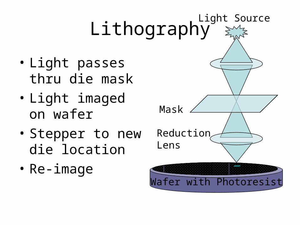
Lithography
• Light passes thru die mask
• Light imaged on wafer
• Stepper to new die location
• Re-imageWafer with Photoresist
Mask
Light Source
ReductionLens

MS&E vs ChE
• How is a Materials Science and Engineering Education Different from Chemical Engineering Education?– Focus on Solids Processing
• What Crystal Structure
– Higher Purity Materials– Impurities Control Properties
• Semiconductors• Grain Boundaries
– Where atoms are in structure determines properties

Where Thermodynamics Comes into Chip Processing
• Evaporation Rate during Spin Coating• Evaporation Rate during Photoresist Drying• Metal Physical Deposition• Chemical Vapor Deposition
– Feed of TEOS– Rxn of TEOS
• Etching - SiF4 vapor pressure
• CMP Solution Equilibria– Dissolution/Precipitation

Lithography
• Light passes thru die mask
• Light imaged on wafer
• Stepper to new die location
• Re-imageWafer with Photoresist
Mask
Light Source
ReductionLens

PhotoLythography
PhotoResist UV light=193 nm 80 nm Line
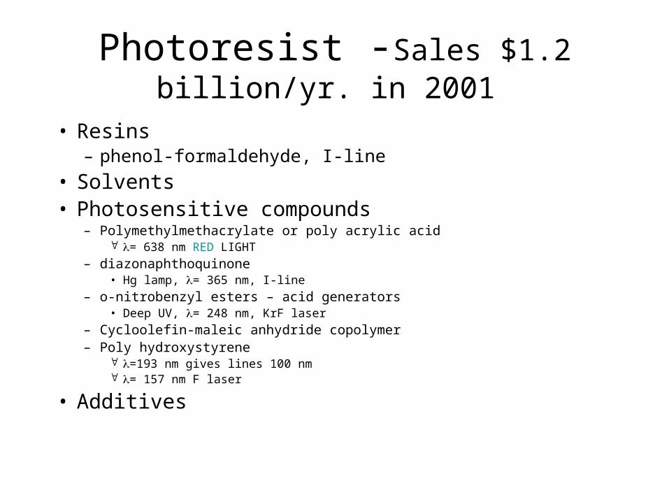
Photoresist -Sales $1.2 billion/yr. in 2001
• Resins– phenol-formaldehyde, I-line
• Solvents• Photosensitive compounds
– Polymethylmethacrylate or poly acrylic acid = 638 nm RED LIGHT
– diazonaphthoquinone• Hg lamp, = 365 nm, I-line
– o-nitrobenzyl esters – acid generators• Deep UV, = 248 nm, KrF laser
– Cycloolefin-maleic anhydride copolymer– Poly hydroxystyrene
=193 nm gives lines 100 nm = 157 nm F laser
• Additives

Photoresist
• Spin Coat wafer
• Dry solvent out of film
• Expose to Light
• Develop
• Quench development
• Dissolve resist (+) or developed resist (-)

Spin Coating
• Cylindrical Coordinates– Navier-Stokes– Continuity

Newtonian Fluid-non-evaporating
2/1
22
322
32
0
22
2
3
41)(
)0(..
3
1
)(3
),(@0
0@0
.'.
thhth
solution
hthCB
hrrr
qrrrt
h
thdzvq
trhaz
v
zv
sCB
rz
v
oo
o
h
r
r
r
r
If hois a constant film is uniformFor thin films, h -1 t-1/2

Evaporation Model - Heuristic Model
• CN non-volatile, CV volatile
• e = evaporation rate of volatile component
– ei = kMA(Psolvent-I - 0)• q = flow rate

Evaporation Rate
• What is Psolvent-i in a mixture?
– Other solvents and non-volatile components
• fil = fi
v equilibrium condition
– fiv =yiP
– fil = γ i xi Pi
sat
– ln γ i =GiE/(RT)

Vapor Pressure of 2 solvent mix
• P =Σ γ i xi Pisat = γ 1 x1 P1
sat + γ 2 x2 P2sat
• y1 =P1/P= γ 1 x1 P1sat /(γ 1 x1 P1
sat + γ 2 x2 P2sat )
• Pisat obtained from Normal Boiling Point & Heat of
vaporization (Claperon Equation)
• Eqs 12.10 a Margules equation, GE/(x1x2RT)=A21X1+A12X2 1 x1 T exp 1 x1 2 A12 2 A21 A12 x1
Tln Psat d
d
HV T( )
Rg T2
2 x2 T exp 1 x2 2 A21 2 A12 A21 x2

See MathCad Example
• Vapor Pressure of Solvent Mix.mcd
• Binary Solvent Mixture
• Ternary mixture of Solvent plus Non-volatile Resin

Next StepDissolve Edge of Photoresist
• So that no sticking of wafer to surfaces takes place– Wafers are stored in a rack on edge
• So that no dust or debris attaches to wafers
Wafer with Photoresist

How would you set up this problem?
• fil = fi
s equilibrium condition– fi
s = γsi zi fs
i
– fil = γl
i xi fli same a previous example of solvent mix
– ln γl i =GiE/(RT) same a previous example of solvent mix
• γli xi fl
i = zi γsi fs
i
• γli xi = zi γs
i Ψi Chapter 14
• Ψi = exp{(ΔHisl/R)[(1/Tm) - (1/T)]} Chapter 14
• ΔHisl =Heat of fusion, Tm melting temperature
• zi γsi=1 for ideal solid (misicible)
• zi= mole fraction of mix in solid
Break
• Second lecture is next
• What did we learn
• Calculate the partial pressure– Used to calculate the evaporation rate of a
component of a solvent mixture
• Calculate the solubility of a solid in a solvent mixture

Lecture 2
• Metal Deposition on the wafer– Wires to connect the transistors and
capacitors • To each other• To outside world
– 2 Mb memory chip has– > 1 km of wire– 8 layers of wiring on top

Deposition Methods
• Growth of an oxidation layer• Spin on Layer• Chemical Vapor Deposition (CVD)
– Heat = decomposition T of gasses– Plasma enhanced CVD (lower T process)
• Physical Deposition– Vapor Deposition– Sputtering

Physical Vapor Deposition
• Evaporation from Crystal (metal)
• Deposition on Wall

Physical Deposition Reactor
• Wafers in Carriage (Quartz)
• Carrier Gasses enter• Pumped out via
vacuum system• Furnace
– Metal evaporated– Sublimation
• No liquid phase
Vacuum
Furnace
Chamber at lower Temp
P
V
s l v

Deposition Rate
• Ratei = Km A {Pi(TF) - Pi(TC)}
• What is the sublimation partial pressure of metal as a function of temperature?
• fiv = fi
s equilibrium condition
– fis = γs
i zi fsi= γs
i zi Pisat exp[VMi(P - Pi
sat)/(RT)]» Poynting Factor
– fiv =yiP


Metal Saturation Pressure
• Sublimation Vapor Pressure– Claperon Equation
• ΔHS is the heat of sublimation
• ΔHS = ΔHF + ΔHV
– solid to liquid then liquid to vapor
Tln Psat d
d
HS T( )
Z Rg T2

MathCad File
• Sublimation Vapor Pressure of Alloy.mcd