theses and dissertations thesis collection and dissertations thesis collection 1986-03 testing...
TRANSCRIPT

Calhoun: The NPS Institutional Archive
Theses and Dissertations Thesis Collection
1986-03
Testing methods for integrated circuit chips
Betoner, Zafer
http://hdl.handle.net/10945/22144


DUDLEY KHOX LIBRARY
NAV/VL P' r.lGHADUATE SCHOOL
MONTEREY. CALIFORNIA 93943-3002


NAVAL POSTGRADUATE SCHOOL
Monterey, California
• THESI (/)
FOFTESTING METHODS
i INTEGRATED CIRCUIT CHIPS
by
Zafer Betoner
.
March 1986
Thesis Advi s o r : M. L. Cotton
AjDprovecl for public release; distribution is unlimited
T226031


fCURirv CLASSIFICATION OP TMIS PCkGE
REPORT DOCUMENTATION PAGE
3 REPORT SECURITY CLASSIFICATION
UNCLASSIFIEDlb. RESTRICTIVE MARKINGS
a SECURITY CLASSIFICATION AUTHORITY
b. DECLASSIFICATION /DOWNGRADING SCHEDULE
3 DISTRI9UTION/AVAILA8ILITY Of REPORT Approved forpublic release; distribution isunlimited
PERFORMING ORGANIZATION REPORT NUMB£R(S) 5 MONITORING ORGANIZATION REPORT NUMB£R(S)
a. NAME OF PERFORMING ORGANIZATION
^aval Postgraduate School6b OFFICE SYMBOL
(If applicable)
62
7a NAME OF MONITORING ORGANIZATION
Naval Postgraduate School
-. ADDRESS (Cry, State, and ZIP Code)
tonterey, California 93943-50007b ADDRESS (Gfy, State, and ZIP Code)
Monterey, California 93943-5000
i NAME OF FUNDING/SPONSORINGORGANIZATION
8b OFFICE SYMBOL(If applicable)
9 PROCUREMENT INSTRUMENT IDENTIFICATION NUMBER
ADDRESS (Gfy, Sfafe. and ZIP Code) 10 SOURCE OF FUNDING NUMBERS
PROGRAMELEMENT NO
PROJECTNO
TASKNO
WORKACCESS
UNITION NO
TITLE (Include Security Classification)
TESTING METHODS FOR INTEGRATED CIRCUIT CHIPS
PERSONAL AUTHOR(S)
jafer Betonera TYPE OF REPORT
Master's Thesis13b TIME COVEREDFROM TO
U DATE OF REPORT (Year. Month, Day)
86 March 2715 PAGE COUNT
84SUPPLEMENTARY NOTATION
COSAfi CODES
FIELD GROUP SUB-GROUP
18 SUBJECT TERMS [Continue on reverse if necessary and identify by block number)IC Testing; Functional Test; Test Methods;Functional Tests
ABSTRACT (Continue on reverse if necessary and identify
Provision for the functional t
nvolves as much design effort ahe hardware requirements for teThis research investigates thehip testing. Available approacoted. Methods of communicationevice under test are examined aontroller
.
Two candidate approaches are seneral-purpose processor with sontroller and (2) a custom VLSIhe device under test. As a resroposed
by block number)
esting of fabricated VLSI chips frequentlys the original chip design itself. Oftensting involve a large expense.logical and functional requirements for
hes are examined and their capabilitiesbetween the test controller and the
s well as logical structure of the test
elected for comparison. (1) A standardtandard bus interface serves as the testtest controller interfacing directly to
ult , a test system architecture is
D 5'^'3U'!'!ON / AVAILABILITY OF ABSTRACTS .'m;la$sifieD'''jnl!mited D same as rpt
121 ABSTRACT SECURITY CLASSIFICATION
Qdtic usersI
UNCLASSIFIED) ".,:.ME OF RESP0NSI3LE INDIVIDUAL
rof M. L. Cottoni22b TELEPHONE (/nc/ude Area Code)
i ( 408)646-237722c OFFICE SYM30'.
62CcIf FORM 1473, 34 MAR 33 APR edition may be used Lintil exnausted
All other editions are obsoleteSECURITY CLASSIFICATION OF "r-iiS PAGE

Approved for public release; distribution is unlimited.
Testing MethodsFor Integrated Circuit Chips
by
Zafer BetonerLt. J. G. , Turkish Navy
B. S. , Turkish Naval Academy, 1978
Submitted in partial fulfillment of therequirements for the degree of
MASTER OF SCIENCE IN ELECTRICAL ENGINEERING
from the
NAVAL POSTGRADUATE SCHOOLMarch 1986

ABSTRACT
Provision for the functional testing of fabricated VLSI
chips frequently involves as much design effort as the orig-
inal chip design itself. Often the hardware requirements for
testing involve a large expense.
This research investigates the logical and functional
requirements for chip testing. Available approaches are
examined and their capabilities noted. Methods of communica-
tion between the test controller and the device under test
are examined as well as logical structure of the test
controller.
Two candidate approaches are selected for comparison.
(1) A standard general-purpose processor with standard bus
interface serves as the test controller and (2) a custom
VLSI test controller interfacing directly to the device
under test. As a result, a test system architecture is
proposed.

TABLE OF CONTENTS
I. INTRODUCTION 10
II. CONCEPT OF TESTING VLSI CIRCUIT CHIPS 13
A. DESIGN VERIFICATION 13
B. TEST GENERATION AND VERIFICATION 13
1. Fault Simulation and Fault Models .... 15
2. Stuck-At Model 18
3. D Algorithm 20
C. DESIGN FOR TESTABILITY 21
1. Ad Hoc Testing 22
2. Structured Design for Testability .... 22
3. Built-in Test And Self-test 25
D. SIGNATURE ANALYSIS 28
1. Signature Analyzing 28
2. Advantages 31
3. Disadvantages 32
4. Other Techniques 32
E. CAD/CAT .. 33
1. System Aspects 34
2. Software Development 34
3. Hardware Selection 35
4. CAD Impact on Design 35
F. TEST EQUIPMENT AND METHODS 37
G. TEST SOFTWARE 43
H. ECONOMY OF TESTING 46
III. REQUIREMENTS FOR TESTING 48
A. FUNCTIONAL TEST STRATEGY 48
B. WHY FUNCTIONAL TEST 49
C. USING SIMULATION DATA AS TEST ANDREFERENCE VECTORS 50

NAVAL POSiii-iuAjJUATE SCHOOLMONTEREY. CALIFORNIA 93943-8002
D. BASIC CHARACTERISTICS OF A FUNCTIONALTESTER .51
IV. FOCUS ON TWO BASIC APPROACHES 53
A. GENERAL PURPOSE MICROPROCESSOR AND BUSINTERFACE 53
1. Objective 53
2. Discussion 53
3. Katz ' s Design Frame 56
4. Results and Analysis 57
B. A CUSTOM VLSI TEST CONTROLLER AND BUSINTERFACE 59
1. Statement of Design Goal 59
2. Major Components 61
3. Structural Floor Plan 62
4. Functional Specification 62
5. Results and Further Directions 65
V. PROPOSED TEST SYSTEM ARCHITECTURE 67
A. HARDWARE DESIGN CONSIDERATIONS OF TESTER ... 67
1. Controller 69
2. Memory Boards 70
3. Programmable Clocks 71
4. Interfaces • 72
B. SUMMARY 72
C. DISCUSSION .'
. . 73
VI. CONCLUSION 76
LIST OF REFERENCES 78
INITIAL DISTRIBUTION LIST 83

LIST OF TABLES
1. REPRESENTATIVE PHYSICAL FAILURES IN ICS 16
2. PARAMETERS FOR CLASSIFYING FAULTS IN DIGITALSYSTEMS 17
3. SOME FEATURES OF 8086 AND 68000 54
4. TECHNICAL FACTORS FOR VARIOUS BUSES 55
5. CELLS USED IN DESIGN OF TESTER 63

LIST OF FIGURES
1.
1
Combinational Circuit 10
1.
2
Sequential Circuit 11
2. 1 Test for input stuck at fault 19
2.2 Shift Register Latch 23
2.3 Typical LSSD Chip 24
2.4 BILBO Usage 27
2.5 BILBO Circuitry 27
2.6 A Linear Feedback Shift Register 29
2. 7 Use of Signature Analysis Tool 30
2. 8 Compact Testing 31
2.
9
VISTA Software Overview 35
2. 10 VISTA Hardware Configuration ' .... 36
2. 11 Simple Test System 38
2. 12 Hardware Approach to IC Testing 39
2. 13 Microprogrammed IC Tester 41
2. 14 VLSI Tester Block Diagram 42
2. 15 CAT System-Software Overview 43
2.16 The ICTEST System ...-.... • 45
2. 17 Basic Flow of Test Process 46
3.1 Automated Tester for VLSI .514. 1 Microprocessor Based Test System 53
4.2 ISBC 86/12A Block Diagram 57
4. 3 The Design Frame 58
4.
4
Master Slave Configuration 59
4. 5 Functional Diagram of IC Tester 60
4. 6 An Example Memory Subsystem 61
4. 7 Floor Plan of Tester 64
4. 8 Final Layout of IC Tester 66
5. 1 Proposed Test System 68

5. 2 Configuration of Functional Tester 59
5. 3 0M2 System Configuration 74
5. 4 Block Diagram of The Data Path Chip 75
8

ACKNOWLEDGEMENT
I would like to express my gratitude to my advisor
Professor Mitchell L. Cotton and my second reader Professor
Donald E. Kirk for their guidances and assistances. And, I
want to thank my wife Hulya, and my daugther Burcu for their
patience and support.

I. INTRODUCTION
The continued and rapid increase in the performance and
complexity of VLSI technology creates a challenge for the
design, development and test of integrated circuits.
This motivation attracts attention to the structured
design methods which make possible the implementation of
VLSI systems with little previous experience. There are
design validation tools available, e.g. , layout languages,
design rule checkers, circuit extractors and simulators.
These tools provide a simple way to simulate and verify the
design. On the other hand, designers have no widespread and
easy to use tools for debugging and testing when they
receive their chip. If prototype chips are to be used in
systems it is essential to verify that the designed chip
performs the intended function successfully. So the problem
of developing a methodology to test the circuits of VLSI
technology efficiently needs to be addressed.
Properly defined test vectors are applied to the inputs
of the device under test and outputs can be compared to a
stored correct response. The simplest testing idea is shown
in Figure 1.1 . In general, 2^ test vectors are required in
this case.
n
InDuts(Test vectors)
DEVICEUNDER TEST
(DUT)
n7^ ^
Outputs(Response vectors)
Figure 1. 1 Combinational Circuit.
10

The test vectors should be carefully selected if they
are to supply relevant information about a chip [ Ref . 1]. A
sequential circuit, as in Figure 1.2, is more difficult to
test, since the output of a sequential circuit network
depends not only on the present inputs but also on the
internal state of the circuit. The number of test vectors
required for this case are 2rn-m
1
1
1
— — — _ _ -_ _J
1
•
nCOMBINATIONAL
LOGIC
1.—1
—
1
Pre^e]State
1
1
1
1
1
1
1
1
r- /1
^
nt
^
Next i
State^
Memory( Flip-Flops
)
A
. >m
^ /
S T1
— - UD E V I
PCLK
C E U N D E R T E
Figure 1. 2 Sequential Circuit.
It is a fact that that test vectors may be generated and
results may be compared in a computer aided environment.
The rest of the chapters investigate testing methods and
systems for integrated circuit chips. In Chapter Two the
most popular and available approaches are examined. Their
11

advantages and disadvantages are noted. The main purpose of
this study is to set basic guidelines and decide on a useful
test strategy for an academic environment. Chapter Three
introduces the requirement of testing and explains why a
functional test strategy is chosen. In Chapter Four, two
candidate approaches for a tester are examined and results
are derived. The first one is a general purpose processor
with standard bus interface and serves as the test
controller. The second is a custom VLSI test controller
interfacing directly to the device under test. Chapter Five
proposes a test system architecture which includes all of
the considerations derived before. Conclusions and
recommendations are given in the last chapter.
12

II. CONCEPT OF TESTING VLSI CIRCUIT CHIPS
A. DESIGN VERIFICATION
Design Verification is a test process which is done
during the design. Following are two definitions of Design
Verification;
" Design Verification Testing involves the simulationof a set of input nodes with a known set of input testvectors and capture of vectors from a set of outputnodes to verify the logical integrity of a design. "
[Ref. 2]
" Design Verification (is the process of) estab-lishing that the logical design of a given digitalnetwork does not contain any timing problems v/hichcould prevent it from performing the intended func-tion under certain conditions. [Ref. 3]
Design Verification is performed to ensure that all
circuit characteristics are compatible, that required speci-
fications can be achieved, and to ensure that no major
design flaws remain. Simulation is employed to check for the
adequacy of the design. In general this may be accomplished
with assistance from a design automation system [ Ref. 4] .
It must be noticed that verification techniques and tools
are used during the design phase. The test capability we
wish to develop, which is different than design verifica-
tion testing, is to verify that the designed chip
accomplishes its intended function successfully.
B. TEST GENERATION AND VERIFICATION
Test generation is the process of searching for a
sequence of input test vectors which verify correct behavior
of the circuit. Test verification is concerned with finding
measures of effectiveness of a given set of test vectors.
13

Test generation is complicated by flip-flops, circuit
initialization needs, asynchronous circuits, indeterminate
states and non-functional inputs [ Ref . 5]. On the other
hand, a complete set of test vectors does not guarantee an
adequate test. All of these considerations should be
addressed when developing a test strategy and a test plan.
As stated in [Ref, 6] , test generation must consist of
three main activities:
1. Selecting a good descriptive model, at a suitablelevel, for the system under consideration. Such amodel should reflect the exact behavior of the systemin all its possible modes of operation.
2. Developing a fault model to define the types of faultsthat will be considered during test generation. Inselecting a fault model, the percentage of possiblefaults covered by the model should be maximized, andthe test costs associated with the use of the modelshould be minimized. A good fault model is usuallyfound as a result of a trade-off between them,
3. Generating tests to detect all the faults in the faultmodel. This part of test generation is the essentialpiece of the whole test process. Generating a testsequence to detect a certain fault in a digitalcircuit usually involves two problems. First, thefault must be excited; i.e, a certain test sequencemust be applied that will force a faulty value toappear at the fault location if the fault exists.Second, the test must be made sensitive to the fault;i. e. , the effect of the fault must propagate throughthe network to an observable output.
It is also important to locate the fault as well as
detecting it. The test strategy is going to be changed,
depending on whether it is desired simply to detect the
fault or both to detect and locate the fault.
The challenge of fault simulation and test verification
problems has received a lot of attention, and the task of
test generation has been partially overlooked. The use of a
random-number pattern generator and generation of a test
which detects a single failure shows the degree of underes-
timation of the iniportance of the test-generation process.
The manual generation of test patterns is a difficult, time-
consuming job even for moderate size circuits. The task of
14

fault simulation and test verification is a bookkeeping,
grading, direction-giving, and fault-dictionary-building
task. [ Ref . 7]
Fault simulation has been the goal of test generation,
yielding a quantitative measure of test effectiveness. In
other words, a test sequence is considered good if it can
detect a high percentage of the possible device under test
faults. It goes beyond logic and timing verification and is
a more complex process. Fault simulation must predict how a
circuit will, or can, fail and if this failure happens, the
test program must be comprehensive enough to find it.
[Ref. 5]
There are lots of algorithms, models and simulations
based on fault detection. Let us review them briefly.
1. Fault Simulation and Fault Models
Extensive studies have been made of the failures
occurring in integrated circuits. These are examined in
[Ref, 9]. This report states that failures have two major
sources: defects in the manufacturing process, and component
wearout. The frequency of occurrence and relative importance
of the various faults depends on the circuit type (TTL, ECL,
NMOS, CMOS, etc. ) and the manufacturing technology used.
Table 1 from [Ref, 9] summarizes the most common IC faults.
Given any physical fault mechanism in a circuit, it
is possible, at least in principle, to determine its effect
on the logical behavior of the circuit. As stated in [ Ref.
9] , there are several advantages to using logical fault
models instead of physical fault models:
1. Once we have a logical fault model that adequatelyreflects the physical failure modes of a circuit,fault analysis becomes a logical rather than a phys-ical problem.
2. It is possible to construct logical fault modelsthat are applicable to many different technologies,m which case fault analysis becomes relatively
15

TABLE 1
REPRESENTATIVE PHYSICAL FAILURES IN ICS
Package wiring faults
On-chip metalization ( aluminum) faults due to:
Corrosion
Electremigration
Microcracks
Bridging
Dielectric (silicon dioxide) faults due to:
Mask defects
Electrostatic discharge
Surface faults
Threshold shifts
Pattern sensitivity
Soft faults due to:
Alpha particles
Cosmic rays
technology-independent. This means that computerprograms tor fault simulation and test generationcan be written that do not lose their usefulness withchanges in technology.
3. Using logical fault models it may be possible toderive tests for faults whose physical" reason isunknown, or whose effect on circuit behavior is notcompletely understood.
16

A logical fault model often covers a large number ofdifferent physical faults, resulting in a substantialdecrease in the complexity of fault analysis.
Various criteria may be used for classifying both
physical and logical faults; Table 2 lists the most
important ones [ Ref . 9].
TABLE 2
PARAMETERS FOR CLASSIFYING FAULTS IN DIGITAL SYSTEMS
Variabi.lity with respect to time:
Permanent
Intermittent
Transient
Number of primitive faults that maly be
present simultaneously:
Single faults
Multiple faults
Effect on components
Effect on interconnections betweenL components
Effect on operating speed
Most of the studies have addressed the single stuck
fault. A commonly used fault model is the Stuck-At model. A
faulty gate input in a circuit is modeled as a Stuck-At-0
17

(S-A-0) or a Stuck-At-1 (S-A-1). When a certain number of
input test vectors are applied to a circuit, the percentage
fault coverage depends on the number of S-A-0 or S-A-1
faults that can be detected by the input test sequence as a
percentage of the total number of single faults that might
happen. Some other fault types are: multiple stuck-at
faults, delay faults, pattern sensitive faults and
short-circuit faults.
2. Stuck-At Model
This model does not take into account all possible
defects, but is a more global type of model. It assumes that
a logical gate input or output is fixed to either a logic
or a logic 1. For example, the faulty AND gate pictured in
Figure 2.1 (b) perceives the A input as 1, even if the logic
value is placed on the input.
The pattern applied to the fault free AND gate in
Figure 2.1 (a) has an output value of since the input is
on the A input and 1 on the B input. But the pattern in
Figure 2. 1 (b) shows an output of 1, since the A input is
perceived as a 1 even though a is applied to that input.
Therefore, the pattern shown in Figure 2.1 is a test for'
the A input, S-A-1, because the good machine
responds differently from the faulty machine. [ Ref . 8]
Techniques are available to decrease the complexity
of fault simulation, however, it is still a time consuming
and expensive task. It has been observed in [Ref. 8] that
the computer run time to do test generation and fault simu-
lation is approximately proportional to the number of logic
gates to the power of 3.
The problem with CMOS is that there are a number of
faults which could change a combinational network into a
sequential network. Therefore, the combinational patterns
are no longer effective in testing the circuit in all cases.
[Ref. 10,11]
18

1
B
(a) Fault Free A2^ Gate.
S-A-1
B
(b) Faulty M>:D Gate
Figure 2. 1 Test for input stuck at fault.
It was noted previously that single stuck-at fault
test sets seem to provide acceptable levels of fault
coverage for devices fabricated with current technology.
Advances in VLSI technology are rapidly changing circuit
characteristics, however, and it would be desirable to
anticipate the effect of these changes on the occurence of
multiple faults. During the fabrication process a single
surface defect or a variation in processing parameters can
cause multiple faults. The major problem in developing test
sets for multiple fault detection is the large number of
possible faults. For example, it is calculated in [ Ref . 12]
that if we have a circuit with only 10 nodes there are 20
single stuck-at faults, 180 double faults, 950 triple
faults, and 59048 possible stuck-at fault patterns. For
19

today's VLSI circuits, which may contain in excess of 100000
nodes, it can be easily seen that explicit test generation
for anything other than single faults is impractical.
In summary, fault simulation has some difficulties
in VLSI circuit applications. The increase in circuit
complexity makes the simulation of all gate-level faults
very time consuming. The gate level description of the VLSI
chip must be available and good documentation is required.
Consideration of only single stuck-at faults may be inade-
quate. Multiple faults, non-stuck type faults and suspended
temporarily at intervals type faults are important
but either difficult or impractical to process. [ Ref
.
9,11,12,13,14,15, 16]
3. D Algorithm
The D-algorithm is a method for generating a test
vector for a given fault. This algorithm, developed by Roth
at IBM, is probably the most widely used test generation
procedure [Ref. 17]. It is typically used with gate-level
circuit models and stuck faults. The D-algorithm attempts to
construct a sensitized path over which an error signal can
propagate from the fault location to an observable primary
output line. It systematically assigns values to lines asso-
ciated with each potential sensitized path until a valid
assignment is found, if one exists. Using a backtracking
approach based on the circuit structure, the D-algorithm
searches the space of possible test patterns for the given
fault. The method in its most general form can always find a
test or, in the case of an undetectable fault, prove that no
test pattern exists for it. [Ref. 9,17,18]
It is v/orth noting that the D-algorithm is particu-
larly well-suited to test generation for circuits designed
using LSSD (Level Sensitive Scan Design) and similar tech-
niques. A large number of practical test generation programs
and algorithms are based on the D-algorithm. [Ref. 9J
;o

With the vast increase in circuit density, the
ability to generate test patterns automatically and conduct
fault simulation with these patterns has decreased. As a
result, some manufacturers are skipping these more difficult
approaches and are accepting the risks of shipping a defec-
tive product. One general approach to reduce the cost of
testing is embodied in a collection techniques known as
Design for Testability. [ Ref . 8]
C. DESIGN FOR TESTABILITY
Design for testability is motivated by the need to
reduce the costs associated with testing and maintaining a
digital system over its working life. Major testability
considerations include test generation difficulty, test
sequence length, test application cost, fault coverage and
fault resolution. The costs are basically those of the
computer time required to run test pattern, personnel to
write the test pattern programs and test equipment [ Ref. 9]
.
The objective is to design circuits from the outset so
that test verification and test generation efforts are
limited in magnitude [ Ref. 10]
.
Testability relies on designer awareness of two concepts
called controllability and observability. Controllability is
the ability to set and reset every node internal to the
circuit. Observability is the ability to observe either
directly or indirectly the state of any node in the circuit.
There are programs that can compute controllability and
observability for a given circuit [Ref. 19,20].
Three basic approaches to design for testability are ad
hoc testing, a structured design approach, and self-test and
built-in testing.
21

1. Ad Hoc Testing
Common techniques involve partitioning large
sequential circuits and adding test points, but are not
directed at solving the general sequential problem. The use
of test and control points which attempt to improve local
observability and controllability is basic guideline. Ad
hoc techniques usually offer relief, and their cost is prob-
ably lower than the cost of the structured approaches. The
ad hoc approaches use partitioning, test points, bus-
structured design and signature analysis. [Ref. 8,10]
2. Structured Design for Testability
With the utilization of LSI and VLSI technology, it
has become apparent that even more care has to be taken in
the design stage in order to ensure testability and produce-
ability of digital circuits. Most structured design prac-
tices are built upon the concept that if the values in all
the latches can be controlled to any specific value and
observed with a very straightforward operation, then the
test generation, and possibly the fault task, can be reduced
to that of doing test generation and fault simulation for a
combinational logic network. It is stated in [Ref. 8] that
several companies have been dedicating significant amounts
of resources toward Structured Design for Testability. They
have recognized that unstructured designs lead to
unacceptable testing problems.
The most common techniques under structured design
concept are: LSSD (Level-Sensitive Scan Design), Scan Path,
Scan-set Logic Structures and Random Access Scan techniques
[Ref. 8,9,21,22]. We only review the most popular
approach -- IBM's LSSD discipline.
22

a. Level Sensitive Scan Design
With LSSD, the only type of storage element
(other than arrays) permitted in a logic design is the SRL
(shift register latch). Figure 2.2 from [ Ref . 22] shows a
typical SRL configuration. An SRL is a pair of polarity hold
latches with the output of the first latch, LI, permanently
connected to the data input of the second latch, L2. AIs
represent and-invert gates and Ns represent nor gates.
[Ref. 8,22]
Acm
1
L 1 —-11
1
1
Al
1
L21
1
j1
N
1
•1
^r\ ATA 1
Al.
N I
^ ^
1
*-L1
fACLK
—
N >>-<
>
Alrsj
NAl
1 1
i^
N
^ -L2'-''
! 1
••C CLK— N
1
I
1
Al N
1
11 J '
1 f " '
, • Lz
r
N+BCL
1_. J
Figure 2. 2 Shift Register Latch.
The LI latch can be set either by the system
data/clock or by the scan data/A clock because it functions
as a storage element during system operation and as a compo-
nent of the LSSD shift register during testing. All the SRLs
on a chip are connected into a shift register with the input
23

to the first SRL designated Scan Data In and the output of
the last SRL L2 latch designated Scan Data Out. In Figure
2.3 from [ Ref . 22] the dashed line represents the shift
path. Two chip inputs for the non-overlaping scan A and B
clocks are connected in common to the SRLs LI and L2. The
designer has lost the use of four chip pins and the circuits
required to implement the L2 latch and associated clock
drivers, but the connection of the SRLs into a shift
register in no way interferes with the normal functional
operation of the chip. The four pins and the L2 latches
enable the test system to control and retrieve the contents
of any storage element on the chip by a simple shift
technique.
SCAN DATA IN o-
A CLOCK o-
B CLOCK o-
PRIMARY INPUT o-
PRIMARY INPUT o-
PRIMARY INPUT o-
C1-A-
- A
LI
B— L2C2- LI
B—
i
CVA-
L1
CI— LI
B—
I
L2
PRIMARYOUTPUT
PRIMARYOUTPUT
-OiCAN DATA OUT
Figure 2.3 Typical LSSD Chip.
;4
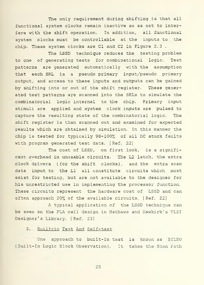
The only requirement during shifting is that all
functional system clocks remain inactive so as not to inter-
fere with the shift operation. In addition, all functional
system clocks must be controllable at the inputs to the
chip. These system clocks are CI and C2 in Figure 2.3 .
The LSSD technique reduces the testing problem
to one of generating tests for combinational logic. Test
patterns are generated automatically with the assumption
that each SRL is a pseudo primary input/pseudo primary
output, and access to these inputs and outputs can be gained
by shifting into or out of the shift register. These gener-
ated test patterns are scanned into the SRLs to simulate the
combinatorial logic internal to the chip. Primary input
stimuli are applied and system clock inputs are pulsed to
capture the resulting state of the combinatorial logic. The
shift register is than scanned out and examined for expected
results which are obtained by simulation. In this manner the
chip is tested for typically 98-100% of all DC stuck faults
with program generated test data. [ Ref . 22]
The cost of LSSD, on first look, is a signifi-
cant overhead in unusable circuits. The L2 latch, the extra
clock drivers (for the shift clocks), and the extra scan
data input to the LI all constitute circuits which must
exist for testing, but are not available to the designer for
his unrestricted use in implementing the processor function.
These circuits represent the hardware cost of LSSD and can
often approach 20% of the available circuits. [Ref. 22]
A typical application of the LSSD technique can
be seen on the PLA cell design in Mathews and Newkirk's VLSI
Designer's Library. [Ref. 23]
3. Built-in Test And Self-test
One approach to built-in test is known as BILBO
(Built-in Logic Block Observation). It takes the Scan Path
25

and LSSD concept and integrates it with the Signature
Analysis concept [ Ref . 24]. A 3-bit register is shown in
Figure 2.4 from [Ref. 10] with the associated circuitry. In
mode A (Cq = C, =1), the registers act as conventional
parallel registers. The a^ values are loaded into the L'^
, and the outputs are available on Q ^ . In mode B ( Cg = C,
= 0), the registers act as scan registers. In mode C ( C^ =
1, C^ = 0), the registers act as a signature analyzer or
pseudo-random sequence generator (PRSG). The registers are
reset if Cq = and C^ = 1. Thus a complete test generation
and observation arrangement can be implemented as shown in
Figure 2.5 , [Ref. 10]. The BILBO register on the left is
used as the pseudo-random sequence generator. Its outputs
are applied to the combinational circuitry. The combina-
tional circuitry response are stored in the BILBO register
on the right which is used as a signature analyzer. After a
certain number of patterns have been applied, the signature
is scanned out of the BILBO register and compared against
the actual data. [Ref. 8,10]
In LSSD or other structured design techniques, a
considerable amount of test data volume is involved with the
shifting in and out. With BILBO, if 100 patterns are run
between scan-outs, the test data volume may be reduced by
factor of 100. The overhead for this technique is higher
than for LSSD since about two EXCLUSIVE-OR' s must be used
per latch position. Also, there is more delay in the system
data path.
Other techniques that are going to be introduced
very briefly, are Syndrome Testing and Autonomous Testing.
In syndrome testing, which requires exhaustive testing, all
possible inputs are applied to the circuit and the number of
I's at the output are counted. The resultant value is
compared with that of a known good machine. Extra circuitry
26

MUX »•
<JV
::^>^-
.OGlC D.A3MAM FOR A 3 B^T BilBO
1d„
Figure 2. 4 BILBO Usage.
PSEUDO-RANDOMSEouE^:cEGENERATOR
COMBINATIONALCIRCUITRY
S I GNATUREANALYZER
-
Figure 2. 5 BILBO Circuitry.
includes a pattern generator, a counter, and a comparison
circuit. [ Ref . 8,10,25,26]
On the other hand, in the autonomous test approach,
modules are partitioned into small modules, which are then
tested exhaustively. [Ref. 8,10,15]
27

D. SIGNATURE ANALYSIS
Compact testing methods attempt to solve the problem of
analyzing and storing the large amount of response data
which is required for a good response generation. It is
possible to compact response data R into a form f(R) which
includes most of the fault information. This eliminates the
need for a large memory and additional circuit units.
A general form of a signature of the data a,b,c,... is
any function f ( a, b, c, . ..
) . This function can be used as
sufficient evidence of the presence of a particular data
set, just like a person's signature on a check. It's not
absolute proof of the presence of the data, however.
The signature analysis technique was introduced in 1977
[ Ref . 27]. This technique should only be used when it is
not feasible to compare test result data against actual
data. There is no advantage to using signature analysis if
the actual data is available at the same rate and in
synchronism with the data being tested. It is a useful
tool when properly utilized [Ref. 28].
Regarding the concept of design for testability, it
falls between the ad hoc and the structured approaches for
testable design. It is well-suited to bus structure archi-
tectures, in particular, those associated with microcom-
puters. The key to signature analysis is to design a
network which can excite itself. Such a network could be
microprocessor-based boards, since they can stimulate them-
selves using the intelligence of the processor driven by the
memory on the board [ Ref. 8] .
1. Sicrnature Analyzincr
The initial part of the approach is a linear feed-
back shift register (LFSR). An example of a 3-bit LFSR is
shown in Figure 2.6 . This linear feedback shift register
is made up of three latches. The upper exclusive-or gate
28

takes its inputs from the second and third bit in the shift
register and the result is the input to the first latch. A
LFSR counts for different initial values.
Figure 2.5 A Linear Feedback Shift Register.
For larger shift registers, the maximal length of
the linear feedback configurations can be obtained by
consulting tables in [ Ref . 29] to determine where to tap off
the LFSR to perform the exclusive-or function. Only
exclusive-or blocks can be used, since this preserves the
linearity. The Signature Analysis procedure is external to
the board and a probe is used to probe a particular net on
the board as shown in Figure 2.7.
Let us suppose a bit stream of length n is fed to a
serial data input line. There are 2^ possible combinations
of data streams and each one will be compressed to one of
the 2^ possible signatures. An LFSR has the property of
equally distributing the different combinations of data
streams over the different signatures [ Ref. 30] . For
example, for n = 3 each data stream will be mapped to a
distinctive signature (one-to-one mapping).
For n = 4 exactly two data streams will be mapped
to the same signature. Thus, for a particular data stream
29

Figure 2. 7 Use of Signature Analysis Tool.
(good response), there is only one other data stream (a
faulty output response) that will have the same signa-
ture; i.e, only one faulty response out of 2''" - 1 possible
faulty responses will not be detected.
In general, for any response data stream of
length n > 4, the probability of missing a faulty response
when using 3-bit signature analyzer is
r\-3,
Z -1 ^ z^Z^-i
for n >> 4
It has been shown that the probability of detecting
one or more errors is extremely high if a 16-bit LFSR is
used [ Ref . 6]
.
The question is: if there were errors present at one
or more points in the string of observations of that
particular net of the board, would the value stored in the
shift register (for each latch) be different than the one
30

TEST, PATTERNS
^DUT ^ RESPONSESR f(R)
ERRORSIGNALS
GOOD VJ
iRESPONSES\
(COMPRESSED)
Figure 2. 8 Compact Testing.
for the good machine ?. For each compression function f
shown in Figure 2. 8, there is a slight probability that a
response Rl different from the fault-free response RO which
will be compressed to a form equal to f(RO),i.e. , f(Rl) =
f(RO). If this happens, the fault causing the device under
test to produce Rl instead of RO won't be detected.
2. Advantages
The major advantage is that this approach does away
with the requirement for the actual data at the actual rate
and in synchronism, and the requirement for testing of
functionality. This reduces the cost [ Ref. 28]
.
The hardware to compute typical signature functions
is inexpensive, and can be fast, while at the same time
permitting the go/no-go decision to be made slowly at
software speeds [ Ref. 28]
.
31

3. Disadvantages
The major disadvantage of signature analysis is that
it is difficult to derive any information from the signature
beyond a yes/no decision. It is hard to diagnose failures
from the failing signature. Consequently, a failure in one
node will cause failures to be observed at any other nodes
[Ref. 28].
Most signature functions involve a tradeoff between
the probability of error detection and diagnostic capa-
bility. For example, transition count based functions
provide better diagnostic capabilities than the popular
polynomial function; the latter provides a higher prob-
ability of error detection, but knowing the logical distance
between the expected signature and the failing signature
unfortunately provides no knowledge about the distance
between the expected data and the failing data either in
time ( indicating when the failure might have occurred) or in
space (as to how wrong the failuring data was) [Ref. 28]. .
Another problem with signature analysis is the
volume of information that is contained in the signatures,
even though this is substantially less than the volume of
information . continued in the actual data stream itself. On a
device under test with 1000 nodes, this implies a similar
number of measurement [ Ref. 28] .
4. Other Techniques
There are extensions which use some other tech-
niques in combination with signature analysis. The scheme
proposed in [Ref. 31], called Pseudo-Exhaustive Testing
using Signature Analysis, provides a function independent
testing sequence for sequential machines. Signature and
Parity Testing Techniques can be combined to solve the error
masking problem which arises during the testing of multiple
output circuits. Encoding the contents of the compacting
32

LFSR device using linear block codes is done to recognize
combinations of parity faults in the multiple outputs of the
function [ Ref . 32].
Despite the possibility of missing an error which is
very small (on the order of 0.002 percent), the Signature
Analysis technique requires only very simple hardware
circuitry and a small amount of memory for storing the good
signatures. It is also not sensitive to the order of the
test pattern. Signature Analysis, like any other tool, has
its advantages and limitations but it is useful for testing
if properly applied and combined with other techniques.
E. CAD/CAT
Computer-Aided Design (CAD) of integrated circuits has
had various interpretations as a function of time and defi-
nition source. These interpretations range from use of
simple, interactive graphics and digitizing systems to indi-
vidual programs used for circuit or logic simulation, mask
layout, and data manipulation or reformatting. The computer
aids or tools provide the designer with a rapid and orderly
method for combining and evaluating design ideas and relieve
the designer of numerous routine and design steps. The use
of computer aids in the layout of IC masks essentially
proceeded along two approaches: interactive graphics systems
and automatic layout based on standard cells. Early interac-
tive graphic systems provided a method for capturing the
design by recording coordinate information by manually digi-
tizing and editing data. Methods for superimposing mask
layers, scaling, enlarging, contrasting, and reviewing the
results were expanded to provide fast, sophisticated drawing
commands for constructing, editing, and reproducing complex
figures. [ Ref. 33]
33

In developing VLSI systems with a CAD environment,
system engineering and information processing tasks of many
people must be coordinated. The coming generation of inte-
grated CAD environments is changing the work habits of indi-
vidual designers and operation of VLSI system development
organizations. On the other hand, overcoming the complexity
of advanced VLSI systems requires substantial effort in
organizing many people with increasingly specialized skills.
[Ref. 34]
Some unique CAD principles have been developed and
proven to be very effective when used in conjunction with
other engineering management concepts. As stated in [ Ref.
35] , a number of these principles are summarized below:
1. System Aspects
1. Successful CAD optimizes both individual programs andthe CAD system.
2. The overall CAD system has a higher productivity thanany individual program.
3. Consistent engineer interfaces are imperative.
4. A data base system can improve CAD operation, but anenormously large data base may make the system veryunwieldy and difficult to use.
5. An expert-system may be complex, but a simpler systemmay have only limited usefulness.
2. Software Development
1. The support and tuning of programs are often largertasks than the original development task.
2. Interfacing and debugging is never complete.
3. There is a minimum level of CAD support required,irrespective of the number of people using theprogram.
4. Onlv develop a program if it makes a majorcontribution.
5. Expect programs to change and eventually die.
6. Make sure when starting a project that the capabilitywill be needed when the project is concluded.
34

3. Hardware Selection
There is no ODtimum computer for CAD;it would not be optimum m six months.
if there were,
2. Hardware costs less than software.
3. Distributed computing means moremachine communication.
than machine to
4. CAD Impact on Design
1. CAD must be user driven. CAD must support the presentuser while developing for "Che future.
2. The CAD activity is not a good controller of thedesign process and cannot effectively mediate betweendesigners.
Design iscreativityapproaches.
a creative process and the designers'often leads to differences m design
Engineers stoD verifying and optimizing their projectonly when it is too painful to 'continue.
A5JSPtanonoN
1-
1'.M.r:n
LL'-iR,nsr»«c
1
•
UATX,re — i
PWJCCSS'AeRionoN
Figure 2.9 VISTA Software Overview.
Sophisticated CAD systems have been developed. As a
typical example of CAD for VLSI we provide an overview of
the VISTA (VLSI Simulation Test and Artwork) system which
was introduced in [ Ref 35] . Most of the principles above
were experimentally generated through the experience of
35

designing and implementing the VISTA system whose software
configuration is shown in Figure 2.9 from [ Ref . 35]. A
VISTA workstation consists of a physically small computer
with approximately 1/4 the CPU power of the midi-computers
being used. Each workstation is connected to four intelli-
gent terminals ( Figure 2. 10 ) two of which are color
graphic stations. The entire VISTA CAD system may be run on
the workstation as well as on the larger midi computers.
Larger mainframes are used for batch jobs which consume
extensive computer time. The system is extremely flexible
allowing a user to share computer resources as well as
files. [Ref. 35]
ONC o tMMr
\.OCM. NOOCS
Hinrrttfto woi C0M*Hjrc»S
1
uiMCl siMA>na« MO oCMnonaa m^a
Figure 2. 10 VISTA Hardware Configuration.
The design methodology of' custom VLSI devices,
however, may yield data for test use and may also allow the
device designer to use that data in a semiautomatic manner
on low-volume prototype devices. A successful Computer-Aided
Testing (CAT) system recognizes that design data exists in
many forms during the IC design lifecycle. While device
designers may not have a test background, the test expertise
may be shared by extracting functional pattern data from the
IC design flow and transferring it to the appropriate
36

production test and/or benchtop debuging equipment. Usually
this means capturing the test vectors that were used during
logic simulation and reusing them for test purposes. This
ensures that prototype IC devices can be functionally veri-
fied with the same test patterns used during logic simula-
tion. In CAT design, extendability of the system into other
simulation and testing environments is an important consid-
eration. A properly designed, intermediate pattern format
standard would allow a CAT system to grow into new simula-
tion and test environments without impacting an existing
system. A new logic simulator or piece of test equipment can
be supported by developing a format-conversion program
without re-doing major portions of the existing system. This
concept is important when testing organizations support a
variety of IC design methodologies. [ Ref . 36]
F. TEST EQUIPMENT AND METHODS
Circuit complexity, a large number of inputs, clock
signals and outputs, or the multitude of possible states may
make manual testing prohibitively time-consuming. In general
it will be necessary to use a computer to exercise the chip.
A simple test system is illustrated in Figure 2. 11 .
Properly defined test vectors, provided by the
computer's output port, are applied to the input of the
device under test. The response vector of the device under
test is compared to a stored correct response by the
computer which is programmed to respond with an error
message upon detecting deviation from the expected pattern.
[Ref. 1]
A minimal test system could consist of a general purpose
test board with a tristate driver and read buffer connected
to each pin, a couple of latches to store the state of
the input and/or output variable at each pin, and a
communication interface to the computer. [ Ref. 1]
37

Memory
Input
port
CPU
-J
Output
port
COMPUTER
''rroan^ vgctJf
'TT'tntir'*! v^^or
Clip
ouput
DEMCE U'^T}ER TEST
input
Figure 2. 11 Simple Test System.
A software-based testing system might not be fast enough
to capture some quickly changing response vectors, or it may
have trouble exercising a complex device which may require
some minimum clock rates for proper operation. Higher speed
performance can be obtained with a parallel link to the
computer. ( If the excitation vector is wider than the typical
8 or 16 bit link to the host computer, the vector may be
transmitted in several pieces and assembled in a set of
registers on the interface board). Even higher I/O vector
speeds can be obtained by moving more functions from
software into hardware. An improved tester could use
38

semiconductor memory to store the excitation (test) and
response vectors of a whole test sequence. The captured
response vector can later be analyzed at a slower rate.
[Ref. 1,37]
i
Sequencer 1'''.!t!3!:7f
^
. -rru^ Cr^p
ouiput
DEVICEL"N'DER
TE5T
Chip
input
1
Result
RAMInput
port
— —
x-n'm E\c:unon
R.\MOuiTDut
pon--, ^, _ .
i
COMPIjIHR
-•
IC'Ihis'IhK
•
1
Figure 2. 12 Hardware Approach to IC Testing.
The tester shown in Figure 2.12 from [Ref. 1] is a
peripheral device to the host computer. The two advantages
39

of self contained testing hardware are: first it allows
higher testing speeds and second it frees the computer to
perform other tasks while testing is in progress. The exci-
tation or test vector for the device under test can be
understood as a set of control words emanating from a
computer's control unit, with the result vector out of the
device acting as a condition vector to this control unit.
The tester thus takes the form of a microprogrammed
controller. A tester based on this principle can exercise
very complex devices due to its inherent ability to make
logical decisions based on some of the results. When the
test is concluded, relevant results are as before stored in
a result RAM, and the host computer is signaled to fetch
them. This kind of tester can be adapted to new tasks by
changing the microcode stored in the excitation RAM shown in
Figure 2. 13. The tester may even do suitable branching
dependent on the outcome of a few preliminary tests.
[Ref. 1]
Almost any computer or microcomputer can be used as the
host. The only requirement is that it has an accessible I/O
port. The control unit for the tester could be built using
one of the fast bipolar bit-slice microprocessors. The
proper custom made interface board between the chip and the
test system has to be built and the test routines have to be
written. [ Ref. 1]
One example of a VLSI test architecture is a ZSOOl-based
single board computer with some additional memory and logic,
and an interface to the device under test ( Figure 2. 14 from
[Ref. 38] ). The process involves creating a test program
using the device assembler on a host computer. The program
is downloaded to the VLSI tester where it executes. The
results are captured in a trace memory and are sent back to
the host. The host software then translates the results into
40

. "irojinucn
— f-.'DI ,,
^Uu
\\\SK CONTROI ! F,R
HOSTCOMPUTER
-'
1
1
tdd/es'
EXCITATION RAM1
*Ti:4
cDco'ot *ora
P.peiiae Reiiscer
J L,,,,._.. DEMCEL^DERTEST
iexiici;ejcs'j'j
1
i
coQiTDt word
1JAJLJULi
Progran-jT.aDle Cocki —
-rr-ron -"rr.rr
1
resua .«xr
RESULT RAM
-9^..f ,. ^MT-tn ,
- IC TESTERi
Figure 2. 13 Microprogrammed IC Tester.
a device-oriented test pattern. The operating system allows
the user to load programs to and from a host computer, to
execute programs and to display or edit device under test
41

PSIN'TER01S< DRIVES.
ETC
BUFFER
ASYNCLOGIC
HOSTCOMPUTER
i^
. PS:32
DISruATCRT
CONTROLCRT
ZBCXX)
SINGLE BOARDCOMPUTER
^
SYSTEMINTERFACE
OUTPERIPHERALS
DUT
SYSTEMADDRESS DATA
BUS
TRACEMEMORY4K > 64
COMPAREME MQRV1?ii ^ « 8
PATTERNVtMORY DUT
PROGRAM ASYNC S-'S-'EM
4K . 16 Of CONTROL CONTROLAt. . 3?
Figure 2. 14 VLSI Tester Block Diagram.
registers, memory and test results, and to compare or move
memory blocks. [ Ref . 38]
42

G. TEST SOFTWARE
Testing complex LSI and especially VLSI circuits
requires the generation of a large number of test vectors.
To address these problems, a test software system has been
developed and introduced in [ Ref . 39] . The test software
system consists of three software elements shown in Figure
2. 5 . The first element of the system is the Test Vector
Assembler. It accepts symbolic microcode written in a
register transfer language with many higher level
constructs. These higher level constructs allow the auto-
matic generation of large numbers of test vectors from very
short and simple specifications.
Symbolic
-^Blntry Tfst
CRT l-'NE
CONSOLE PRINTER
TEST
EDITOR
TEST
VECTOR
ac:embler
TEST
VECTOR
SIMULATOR
TEST
VECTOR
EXERCISERMlcrocodt Mlcrocodt V»c tori
->
—
;
i".. J
DUT
Figure 2. 15 CAT System-Software Overview.
The second element of the test software system is the
Test Vector Simulator which contains a software model of the
device under test data paths and storage elements. The model
computes the next state and output configuration of the
device under test based on its current state and the test
43

vectors applied. As a result, the test vectors specified in
the binary microcode are augmented with the corresponding
expected responses, thus completing the test vectors.
The third element of the test software system is the
Test Vector Exerciser software. This program facilitates
interactive control of the actual execution of the test. It
also has special features to aid the test engineer in
performing fault isolation and diagnosis.
The test software system is implemented on an Intel
microcomputer development system computer which is the basis
for an in-house LSI/VLSI test system, the QTS-IV. The
computer itself is based around an Intel 8080 microprocessor
with 64K bytes of memory, dual single density floppy disks,
CRT/keyboard, line printer and integrated circuit test head.
All programs are written in PL/M, an Intel language, and
they run under the ISIS- 1 1 Operating System. [ Ref . 39]
Besides software systems, there are modern test
languages. The extensions that make the following high level
languages into test languages are discussed and introduced
in [Ref. 40,41,42,43,44]. Pascal can be extended for test
pattern generation and special purpose controller program-
ming which are tasks that are specific to ATE. Pascal-T is
also a test language that permits unlimited control of test
functions while retaining the ease-of-use features of a high
level language. PLT (Programming Language for Testers),
designed by IBM, allows the user to perform functional
testing of a product in an event driven mode at the
functional speed of the product [ Ref. 44] .
ICTEST is an algorithmic language for describing
functional tests of digital integrated circuits [Ref. 45].
The test stimulus and response specification is high level,
with the ICTEST system handling the translation into a test
vector. The idea behind the ICTEST system structure shown in
Figure 2. 16 is to unify testing and simulation. The designer
44

writes one test description that can be compiled for any of
the functional simulators and testers in the system.
Currently, tests target to either of two simulators or three
testers.
(^ ICTEST )
(^INTERFACi)
(Esimj ( Tsim)
fMinimal^ /
^Tester J \
MediumA^ Testery
C TEK ^
Mask Data - Packaged Chips
Figure 2. 16 The ICTEST System.
ICTEST itself, the interface programs, and the esim and
tsim switch level simulators run on a VAX-11/780, The VAX
communicates with the testers over serial links. The MINIMAL
tester can test 40-pin devices at a maximum of 1000 drive or
sense operations per second; the MEDIUM tester, 80 pins at
100000 operations per second; the TEK tester, 64 pins at
5000000 operations per second, all pins simultaneously.
ICTEST is an embedding of testing features in the C
language. C is an Algol-like language which is similar to
Pascal. The full power of C is available for describing
tests algorithmically. [ Ref . 45]
45

H. ECONOMY OF TESTING
In general there is always the possibility that a chip
doesn't function as desired. This must be detected through
testing and, if caused by a design flaw, the chip has to be
refabricated and retested. These steps are illustrated in
Figure 2. 17 .
ass
False
jDIAGNOSIS
I
M-REFABRICATE
Figure 2. 17 Basic Flow of Test Process.
There have been some studies concerned with modeling
this process by using algebraic equations [ Ref.
46,47,48,49,50]. The purpose is to determine the effective-
ness of the process and fault coverage of the tester, and to
estimate cost or throughput.
If the cost is $0. 30 to detect a fault at the chip
level, then it would cost $3 to detect that same fault when
46

it was embedded at the board level; $30 when it is embedded
at the system level. With VLSI and the inadequacy of auto-
matic test generation and fault simulation, there is consid-
erable difficulty in obtaining a satisfactory level of
testability. Thus, if a fault can be detected at the chip or
board level, then significantly larger cost per fault can be
avoided at subsequent levels [ Ref . 8]
.
The drop in costs and the increase in throughput occur
as detected faults drop no matter what kind of method is
used [Ref. .46]. On the other hand, faults are not easily
controlled, so much effort has to be spent to reduce them.
Test program development has become an increasingly
complex and time consuming task and development costs are
primarily dependent on programmer and machine time invest-
ments. A remote program management approach has been
proposed to save in manpower and test system utilization.
The benefits and disadvantages of this programming approach
are discussed in [Ref. 51].
Programmer effectiveness and selection of test strategy
are also critical issues for testing. Important productivity
gains can be made in a test organization by improving
programmer effectiveness and selecting a best test strategy
can provide maximum return on investment. These are studied
and quantified in [Ref. 52,53].
It is recommended that critical circuit paths and area
of possible marginal performance be clearly stated prior to
testing. This is contrary to the common belief that only by
revealing such areas of potential weakness is reliable
testing demonstrated. Knowledge concerning possible circuit
limitations allows tests to focus more on these areas while
still providing general tests of circuit functionality. In
this way, the overall effectiveness of testing can be
improved and the cost decreased.
47

III. REQUIREMENTS FOR TESTING
We have considered the most popular currently available
approaches and some systems for testing of integrated
circuits. It is observed that the functional test strategy
is an appropriate approach in an academic environment which
produces a few designs a year. This is why the introduction
of the functional testing approach was left to this chapter.
After examining the functional test strategy, it will be
explained why we decided to use this approach.
A. FUNCTIONAL TEST STRATEGY
Functional testing is basically a test strategy which
attempts to verify correct functional operation of a digital
circuit according to its specifications. A complete test can
be generated considering only the desired operation of a
good system. What is expected from the functional testing
approach is that complex systems can be quickly tested to
see if they perform their intended functions. Functional
faults with respect to functional specifications can be
tested by using a representation of a circuit higher than
its gate level. (We have not encountered any clear and
strong attempts to formalize functional testing). Generally
speaking, functional testing is the differentiation of
faulty integrated circuits from good circuits which satisfy
their functional requirements. An integrated circuit can be
functionally tested by stimulating it with a carefully
defined input test sequence and than comparing its response
with a stored correct sequence.
43
B. WHY FUNCTIONAL TEST
The exhaustive testing approach and the other methods
derived from it often require an unacceptable amount of test
time and memory space to go through all possible steps. A
circuit with 24 inputs and 32 bits of memory has 2^^ or
approximately 4 x 10^ different internal states. There are
2^^ or approximately 16 x 10^ possible input patterns. An
exhaustive test would require approximately 7 x 10*° test
vectors. V7ith the capability of 10 million test steps ( 10
MHz) per second, it would take more than 200 years. Thus,
exhaustive testing is good for only small systems.
Fault simulation and fault modeling techniques are very
useful in describing physical failures in small and medium
scale circuits (especially TTL). However, today's circuits
on a chip may not have a simple correspondence with gate
level logical descriptions. There are many cases where
failures cannot be represented by the stuck-at models [ Ref
.
10] . Representation of a single faulty circuit which has no
simple gate level correspondence would require a large
number of gates. On the other hand, stuck-at models are the
only computationally efficient and quantitative measure of
test effectiveness [Ref. 14]. But when we consider today's
complex LSI/VLSI circuitry this method is time consuming and
requires detailed gate level descriptions of circuits. Since
a detailed circuit description of a chip is often not avail-
able, functional testing becomes important. '
Signature Analysis seems a more economical and attrac-
tive way to perform testing because of data compression and
the requirement of very simple circuitry. Even though the
volume of information contained in this method is less than
the actual data stream itself, it still implies time
consuming measurements.
Once we agree on the functional test strategy which is
the best for our environment under today's circumstances, we
49

can first examine ways of using simulation data as test
and reference vectors and then consider possible basic
characteristics of a functional tester.
C. USING SIMULATION DATA AS TEST AND REFERENCE VECTORS
One way to extract test and reference data vectors is to
drive a tester with ESIM files which are generated during
the design layout phase. This approach, illustrated in
Figure 3.1, is designed and implemented (except for the
communication and hardware interfaces between microcomputer
and tester) in [ Ref . 54] as a thesis project. The ESIM
files for a particular VLSI circuit consist of pin designa-
tions, initialization vectors, clocking sequences, test
inputs and the corresponding output vectors. Test data from
ESIM files are extracted by an "Extract Test Data" software
subsystem. This software program is implemented on a
VAX-11/780 computer system in order not to be restricted by
the memory capability of a microcomputer. This program
changes the available node data into the test vector format,
and writes out these vectors into an external file. This
data file is then converted into the microcomputer operating
system data format and then transferred to an 8" floppy
disk.
The VLSI circuit is simulated either from test files or
from data entered through the keyboard interactively. After
initialization of the tester and the device under test, each
test vector is applied to the device under test and the
resulting response is compared with the given reference
vector.
This method is useful but it is limited by a test
capability that can only test VLSI circuits for which
corresponding ESIM files exist.
50

^ , Test Results
SimulationVector
TTcj-im Ha-hs Pi1*a N.
Microcomputer> 7
Keyboardy*
^
Teste1
. J
Idut
Figure 3. 1 Automated Tester for VLSI.
D. BASIC CHARACTERISTICS OF A FUNCTIONAL TESTER
A typical test plan indicates five basic sequences of
actions as below;
1. Generate the (next) test vector
2. Transmit the vector from tester to device under test.
3. Process the test vectors through the device undertest.
4. Transmit the response from device under test to someresponse analysis circuit or tester.
5. Deduce the received response.
A sequence of these steps may be executed once for every
test vector and every step is executed in one clock cycle.
Keeping this basic plan in mind the most significant
required characteristics of a tester are:
51

1. Sufficient test speed -- A test system with high speedmemory buffering facilitates applying the test vectorsto the device under test. A test system should alsobe capable of testing circuits at their original oper-ating speed.
2. Sufficient number of I/O pins -- As an example the Oiyi2
data path chip has 64 pins [ Ref . 55]. Many of today'sVLSI chips have more than 300 pins.
3. High speed memory buffering with sufficient depth.Today's CMOS memory RAMs have access times of about: 55nanoseconds. The depth must allow one to apply testvectors to the device under test without interruptioncaused by the need of memory reloading.
4. Accurate timing : The timing accuracy must satisfy adelay time of 500 ps or less. The master test clockgenerator circuit and other clock circuits in thetester should be designed to give this accuracy.
5. Ability to provide clocks to the device under test.
6. Ability to synchronize the device under test to thetester. Thisas possible oftester. This may be accomplished by designing as much
the tester with custom VLSI circuits.
-
7. Avoid noise and skew problems which affect testerspeed.
8. Expandability and flexibility. The tester can beeasily reconfigured to improve its capabilities aswell as to satisfy future requirements.
52

IV. FOCUS ON TWO BASIC APPROACHES
Having agreed on the functional test strategy which is
the best for our environment under today's circumstances, we
can start to examine two candidate approaches to design a
functional test system. Chapters Two and Three provide the
basic guidelines.
A. GENERAL PURPOSE MICROPROCESSOR AND BUS INTERFACE
1. Objective
The purpose of this section is to examine the
capabilities of a system shown in Figure 4. 1 and to deter-
mine its hardware and interface requirements.
MicroProcessor
BusInterface <; > DUT
Figure 4. 1 Microprocessor Based Test System.
2. Discussion
The microprocessor controls the complete test
process. The bus interface provides necessary connections
between microprocessor and device under test. We have
chosen two well known microprocessors for comparison. They
are the Intel 8085 and the Motorola 58000. Table 3 lists
53

some of their features and the buses which support either or
both of these microprocessors are listed in Table 4 .
TABLE 3
SOME FEATURES OF 8086 AND 58000
8085 58000
word size( data/instruction) 16/15 15/15
direct addressirange (words)
ng1 MBytes 15 MBytes
max clock freq.( MHz/phases) 5/1 8/1
on chip clock yes no
DMA capability yes yes
package size(pins) 40 54
The test system could operate as fast as the
execution of memory fetch and output write followed by an
input read and memory write. These steps take 40 clock
periods for the 8085 and 40 clock periods in the absolute
addressing mode for the 68000. For only 15-bit test vectors,
a maximum test frequency of approximately 125 KHz for an
Intel 8086 operating at 5 MHz is achievable. This translates
to approximately 200 KHz for an Motorola 68000 operating at
8 MHz. Test vectors of 64-bits would require four of the
previous cycles for each test cycle, indicating a maximum
test frequency of approximately 30-50 KHz. These figures are
dominant and no further calculation is necessary since the
buses are not slower than these data transfer soeeds. Some
54
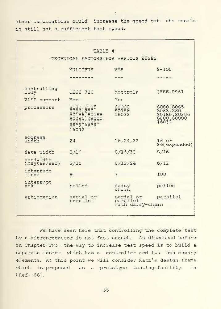
other combinations could increase the speed but the result
is still not a sufficient test speed.
TABLE 4
TECHNICAL FACTORS FOR VARIOUS BUSES
MULTIBUS VME S-100
controllingbody IEEE 786 Motorola IEEE-P961
VLSI support Yes Yes
processors 8080,80858086, Z8080186,8018880286, Z800068000,68006802,68081603^
680008018616032
8080,80858088, Z8080186,802866800.680001603^
addresswidth 24 16,24,32 16 or
24( expanded)
data width 8/16 8/16/32 8/16
bandwidth(MBytes/sec) 5/10 6/12/24 6/12
interruptlines 8 7 100
interruptack polled daisy
chainpolled
arbitration serial orparallel
serial orparallelwith daisy-
parallel
•chain
We have seen here that controlling the complete test
by a microprocessor is not fast enough. As discussed before
in Chapter Two, the way to increase test speed is to build a
separate tester which has a controller and its own memory
elements. At this point we will consider Katz ' s design frame
which is proposed as a prototype testing facility in
[Ref. 56].
55

3. Katz ' s Design Frame
When a fabricated chip is received, it is not easy
to communicate with it. It must be supported for memory and
communications. As stated in [ Ref . 55] , there is a need for
standard design frames for which a user's circuit easily
becomes a prototype system by inserting it into the frame.
The design frame must provide system capabilities like
memory, I/O ports, timers, standard bus, etc. This makes the
testing and debugging of fabricated chips very easy and
saves time.
Katz ' s design frame is based on the Intel iSBC
86/12A single board computer whose architecture is shown in
Figure 4.2, [Ref. 57J . The standard board contains an 8086
microprocessor, 32K bytes of dynamic RAM, three programmable
I/O ports, an RS-232 interface, programmable timers, an
interrupt controller, provision for 15K bytes of ROM, and.
Multibus interface control logic [ Ref. 57] . A feature of the
iSBC 86/12A is that the memory is dual ported between micro-
processor and the Multibus so that a master 8086 on one
board can deposit and examine the memory contents on a slave
board.
Katz ' s design frame is a cannibalized iSBC 85/12A
board and a bus controller that emulates the 8086 's own bus
interface unit [Ref. 56]. The 8086 is simply removed and
the user circuit/bus controller combination chip is plugged
into the 8086 socket as shown in Figure 4.3 from [Ref. 56].
The bus controller acknowledges request signals and gener-
ates bus control signals that are identical to those of the
8086. The other subsystem on the board (I/O ports, memory
chips, Multibus controller, etc. ) behave as though they
are interfaced with an 8086.
56

r^Ts
m
/V>,
II
^ s
'>
\
•'.::.:v.r
/'1
\
n
Figure 4.2 ISBC 86/12A Block Diagram.
As shown in Figure 4. 4, a master slave configuration
of two boards communicating through the Multibus seems prom-
ising as a test system. The master board can download data
into the slave's memory and read data placed in the memoryby the slave. This makes it possible to test fabricatedchips.
4. Results and Analysis
Using the design frame approach provides a testerwith a maximum test speed of approximately 90 KHz. A 6-byte
instruction queue provides pre-fetching and reduces the
instruction cycle. This is why little improvement is
observed in speed. Since the 8086 has 40 pins and the bus
controller uses 12 of them, the tester would have 28 test
57

uuuuu
titt t ittt
USERCIRCUIT
DESIGN FRAME DIE
I 40 PIN DIP—
^
—/n-^
iHi tf t t t l t in tt ti t f ^ f 1 1 1 i
;
•; f
Figure 4. 3 The Design Frame.
pins. The iSBC board has 32K x 8 bits RAM and it is also
expandable to 64K bytes with the iSBC 300 32K bytes
Multimodule RAM option. The power requirement is about 55
Watts. [ Ref . 57]
The advantage of this approach is the capability of
easily communicating externally through the Multibus. In
this way the tester can be interfaced to a design station.
But the test speed and the number of test pins on this
tester are not sufficient.
58

DUT and Bus Controller
SLAVE
OMULTIBUS
<^
8086
Figure 4. 4 Master Slave Configuration.
B. A CUSTOM VLSI TEST CONTROLLER AND BUS INTERFACE
Let us now consider another approach. During a course on
a VLSI design a simplified design of an integrated circuit
tester was developed to reveal the advantages and
disadvantages of this approach.
1. Statement of Design Goal
The goal is to design an integrated circuit tester
using nMOS technology by implementing the simplest testing
approach: apply properly defined test or excitation vectors
to the device under test and compare the outputs to a stored
correct response. A simplified diagram of the tester is
shown in Figure 4.5 All major components are available from
Mathews and Newkirk' s designer's library [ Ref . 23].
59

MUX
/4 /i
CONTROLLER(PLA)
>i
'' 4_i
EXICTATIONRAM
4x8
next addresi;
condition select
condition vector
initial.
interrupt
write
vector
control word
RESULT RAM
4x4
result
vector
1 from/ < HOST
COMPUTER
1 to-4——> HOST
COMP.
8 from/ < HOST
COMP.
excitation 4/ >
"7
1^ >
toDUT
4 from—i—< DUT
4 to-4—\ HOST
' -^ COMP.
Figure 4. 5 Functional Diagram of IC Tester.
60

2. Major Components
There are two basic components in this design;
memory cells and a pla cell.
Memory Cell :
The memory RAM is composed of three cells which are
an Address cell, an InterfacePair cell and a RamPair cell
( Figure 4. 6 )
.
RamPair ( 28 x 33 )
Read from RamPair: B^q has to be precharged and when
the Readbar input is clocked the inverted value stored in
ram cell appears on B'^ .
Write into it: B (^ is driven to the desired value
and Writebar is clocked.
Dr i ve
s
i r
\0
X"
J-CK
O.
^ bGnse
^ Precharge
^ Wr I T ejDor
^ Read_bar
Figure 4. 6 An Example Memory Subsystem.
51

InterfacePair ( 33 x 128)
This cell provides the circuitry necessary for the
outside world to access the ram cell. InterfacePair
precharges B^q during first clock phase. It reads out during
the second clock phase when Sense is clocked and writes in
during the second clock phase when Drive is clocked.
Address ( 24 x 137 )
This is a driver for the Read and Write control
lines. Address qualifies the Readbar and Writebar clocks
with the Selbar line and provides supperbuf fered drive.
Pla Cell :
The pla cell is used to implement the controller,
which is a simple sequencer in this case. All the inputs and
outputs are clocked.
3. Structural Floor Plan
The cells used in this design are listed in Table 5
and the floor plan of the tester is shown in Figure 4. 7. The
system has a total of 32 interconnection pads. The boundary
of the chip is 1186 by 1035. The pla controller and RAMs are
placed in the middle. PadMux pads are used is to reduce the
number of pads required. A PadMux cell acts like an input
pad when its OUT/INbar input is low, and like an output pad
when OUT/INbar is high. The final layout of the tester is
shown in Figure 4. 8 .
The power consumption of this design is estimated by
power estimation program (Powerest). Its estimated average
power is 99. 36 mWatts and the maximum power is 178. 98
mWatts.
4. Functional Specification
The host computer loads the desired 8 bit long
vector into the excitation RAM. After this is done, the host
62

TABLE 5
CELLS USED IN DESIGN OF TESTER
Name Size Amount Cif No:
PadGndPadVddPadOut4Padln4Padr^ux
100 X80 X
100 X100 X100 X
106100145106180
111
209
206207204205282
RamPairInterfaceAddress
28 X33 X24 X
33128137
2468
505506503
InvSB4 20 X 42 1 234
Pla 148 X 79 1 501
computer initializes the controller. The excitation RAM
supplies the next address and enables the controller to
sequence through testing. A 4-bit vector is applied to the
input of the device under test. A 4-bit result vector from
the device under test is stored in the result RAM. Nand
gates are used to implement the multiplexer. It is used to
detect the case when all bits of the result vector are low.
If the condition select bit is programmed to be high at any
desired sequence of testing, this high signal enables the
multiplexer. So whenever the result vector bits are all low
after the multiplexer is enabled, the output of the multi-
plexer terminates the testing sequence. Either in this
condition, or when the test sequence is completed, the
controller interrupts the host computer. The host computer
gets the result vectors from result RAM , analyzes the
results and makes a decision about the device under test.
The only testing simulation done was the test of
writing into and reading out of the RAMs. (Complete func-
tional behavior of the tester depends on the interfaces with
53

'"'** ^•«ln*. ••«ln*j
1»lfllnfc
1
•01»<.
l«ll 142) I*t J ItOl (Mrltt J ,.r..».r,., lon.ti
••ai-*
»aacn<
lianta 1
(•taOut*»•«««
(Mlf)
i
Address ?J^^••IM ••«««
Il(il«)1 l«'Oul)
'••Ir** Interface
ic;)
<C1) ' I"/Out 1
^«In*
-"',E.,
(CT) ?LA ^ l»-Q,.ll
»ialr^•
ICS) [ l-/Ogtl
'•Oli» Address ......
(C«l1
^irc
'••11^ RAM Interface Hol"«
(CSI.
->ITC
( Inl
,
•«ln«
-11 It
^•«MWM
tail
'•Mm!
lall
^•«1M »»«I«4 ^«|n4
•cu> CAS • €»B •CO
(Maatfl (^racncrial (lanialCl./OuO
1
( Ii»/Owl 1
Figure 4. 7 Floor Plan of Tester.
64

the host computer, and the device under test is very
complicated to simulate). Simulation results, however, show
that the RAMs are functioning correctly.
5. Results and Further Directions
This tester has approximately 1 MHz test speed, 4
bits memory depth and 9 I/O pins. This methodology is
effective but not practical from the application point of
view. On the other hand, it can be easly expanded. The
multiplexing idea can be extended to a desired complexity.
The RAM dimensions can be increased to a desired size by
iterating more memory cells.
However, we note that it is really not desirable to
design a complete tester as a custom VLSI circuit. The
tester circuit itself will be complex and hard to test. It
also violates flexibility and expandability requirements.
It is observed that a better way is to design a controller
and other necessary internal interface circuits as a custom
VLSI circuit. Separate high speed CMOS RAMs can be used as
excitation and result memories . This increases flexibility
and makes tester speed depend on basically the access time
of the memory.
65

»3I
^qr
ITI2i
is;
lE:
^ilB^^:^!.! 'I ;: i-\
X Jl b «r—< t^-S
a
tx
rrrr—j- H t-j- i' ^
Figure 4. 8 Final Layout of IC Tester.
65

V. PROPOSED TEST SYSTEM ARCHITECTURE
So far two testing approaches have been examined and
operating characteristics have been derived, A test system
architecture will now be proposed to meet these guidelines.
The logical structure of the controller and interface
requirements between the tester and device under test will
be examined. The speed, memory depth and the number of the
I/O pins of the tester are basic considerations.
A system configuration of the proposed test system is
presented in Figure 5. 1 . A controller, memory board,
programmable clocks, pipeline registers, and device under
test board are parts of the tester. It is a combination of
two basic approaches. The microcomputer can be a Z-100 or
IBM PC and the microprocessor can be an Intel iSBC 86/12A
single board computer. The microcomputer provides the oppor-
tunity for a high-level interface with the other portions of
the tester and through the ethernet to other computer-aided
design systems. This allows, for example, test programs to
be written in high-level languages and a menu-driven user
interface. This is the basic picture of the proposed test
system architecture. First the functional tester of the
system will be presented and then the presentation of the
system will be completed with a scenario based on test
consideration for the 0M2 Data Path Chip designed at Caltech
[Ref. 55] .
A, HARDWARE DESIGN CONSIDERATIONS OF TESTER
A possible logical configuration of the functional
tester is shown in Figure 5. 2 , The tester can communicate
with the microprocessor via the Multibus, The microprocessor
67

ETHERNET
MICRO /v-
COMPUTER \j-
PROGRAI-IMABLE
CLOCKS-:>
-:>MICROPROCESSOR
7T
MEMORY BOARD
±^
CONTROLLER
li-, >
PIPELINE
-> DEVICEUNDERTEST
Figure 5. 1 Proposed Test System.
downloads test vectors into the excitation RAM before the
test phase. The test phase is considered as the process of
applying test vectors and receiving response vectors without
interruption. The microprocessor initializes the controller
to start the test phase. Before getting into more detail let
us examine the basic blocks.
68

ARBITRATIONLOGIC
7>T\
-^
y
MULTIBUSINTERFACE
I
TIMINGANDCONTROLLOGIC
Tf
EXCITATION
RAM
RESULT
RAM
If
<Jl
PIPELINE REGISTERS
ITPROGRAMMABLE
CLOCPCS
^TULTIBUSDATATPJ'.NSCEIVER
<Z
^->
CONTROLLER
TF
MULTIBUS
^-y
m<l-H
oPI
Dm
>n
Figure 5. 2 Configuration of Functional Tester.
1. Controller
The controller must provide at least three
functions. First is the the generation of control signals
for the timing and control logic circuit and the device
under test interface circuit. The second function is address
generation for the memory RAM. The third is generation of an
69

interrupt signal to the microprocessor when the test phase
is completed.
The required control signals from the controller are
addresses for the RAM, start test phase signal, interrupt
signals to the microcomputer, the strobe signal to pipeline
registers, RAM write and read signals, and so on. Complex
address generation to provide branching and conditioning is
not considered here. Simple address generation will be
sufficient for our purposes. Since it is possible to create
test vectors using high level language programs on a micro-
computer, trying to make logical decisions based on some
results during the test phase would only cause confusion and
complexity. At least at the begining, straightforward
address generation is preferred. The controller can be
designed as a PLA implementation of a finite state machine.
2. Memory Boards
Memory boards buffer the data vectors prior to
transfer to and from the host computer and the device under
test. As discussed before, there must be two different
memory blocks. The first one is the excitation or test
vector RAM and the other is the result RAM. Typical commer-
cially available 2K x 8 bits CMOS random access memory
elements have approximately 55 nanoseconds of read and write
cycle time. As a first approximation, this means that an 18
MHz test speed is possible. During the test phase, the
write signal to the excitation RAM and the read signal to
the result RAM may be inhibited by control signals. This
makes the excitation RAM a read only memory and the result
RAM a write only memory during the test phase. So test
vectors could be applied to the device under test and result
vectors could be written into the result RAM without
interruption.
70
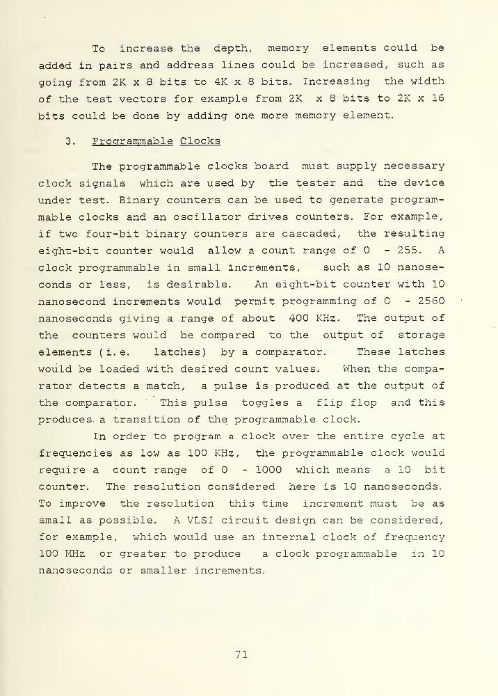
To increase the depth, memory elements could be
added in pairs and address lines could be increased, such as
going from 2K x 8 bits to 4K x 8 bits. Increasing the width
of the test vectors for example from 2K x 8 bits to 2K x 16
bits could be done by adding one more memory element.
3. Procrrammable Clocks
The programmable clocks board must supply necessary
clock signals which are used by the tester and the device
under test. Binary counters can be used to generate program-
mable clocks and an oscillator drives counters. For example,
if two four-bit binary counters are cascaded, the resulting
eight-bit counter would allow a count range of - 255. A
clock programmable in small increments, such as 10 nanose-
conds or less, is desirable. An eight-bit counter with 10
nanosecond increments would permit programming of - 2560
nanoseconds giving a range of about 400 KHz. The output of
the counters would be compared to the output of storage
elements (i.e. latches) by a comparator. These latches
would be loaded with desired count values. When the compa-
rator detects a match, a pulse is produced at the output of
the comparator. This pulse toggles a flip flop and this
produces, a transition of the programmable clock.
In order to program a clock over the entire cycle at
frequencies as low as 100 KHz, the programmable clock would
require a count range of - 1000 which means a 10 bit
counter. The resolution considered here is 10 nanoseconds.
To improve the resolution this time increment must be as
small as possible. A VLSI circuit design can be considered,
for example, which would use an internal clock of frequency
100 MHz or greater to produce a clock programmable in 10
nanoseconds or smaller increments.
71

4. Interfaces
The first consideration here is the interface of
device under test to the tester. Connecting test data lines
coming from memory RAMs to device under test is possible by
using pipeline registers. Typically, the set-up and propaga-
tion delay time of an SN74373 is approximately 15 nanose-
conds. This is important because the speed of the tester is
also dependent on this delay as well as memory access time
and the address generation time for memory.
The device under test interface board should allow
routing any of the data lines received from RAMs, program-
mable clock lines, Vdd, and GND to any pin of the device
under test. The device under test interface and pipeline
registers can be designed together as a custom VLSI circuit.
An arbitration logic circuit must simply allow the
Multibus and the controller to share memory address lines
and separate address lines from the Multibus interface
circuit and connect them to the controller before a test
phase is started.
The timing and control logic circuit must provide
all signals necessary to control the dynamic RAM (i.e. read
and write signals, etc. ), a refresh timer and perhaps
refresh counter. For instance, one of the functions of the
Intel 8202 Dynamic RAM Controller is to provide these
control signals [ Ref . 58].
B. SUMMARY
The expected characteristics and capabilities of the
proposed test system can be summarized as follows. The
maximum possible test speed would be approximately 10 MHz.
As stated before, approximately 55 nanosecond memory access
time, approximately 15 nanosecond delay time of pipeline
registers, and about 25 nanosecond address generation time
72
J

make the 10 MHz approximate test speed possible. Memory
depth could be expanded up to IM byte since 20 bit address
lines are available. Up to 128 test pins could be provided.
These figures are good enough for our purposes. For example,
with such a tester it would be possible to test the 16 bit
0M2 data path chip, [ Ref . 55], which will be discussed next.
C. DISCUSSION
Testing of the 0M2 data path chip can be accomplished by
this proposed test system. The 0M2 16 bit data path chip
contains 16 registers, an ALU, and a 16 bit shifter, and is
designed as part of an LSI computer system, ( Figure 5.
3
from [Ref. 55] ). The data path chip performs most of the
data manipulation functions for the system. The operations
are performed as directed by sequences of control microin-
structions, which are fetched from a microcode memory
using addresses generated by the controller chip.
The 0M2 data path chip has two data ports for
communication with the external system and a communication
path to the controller chip. A block diagram of the 0M2 data
path chip is shown in Figure 5.4 from [Ref. 55]. The data
ports are tristate with either internal or external control.
Communication with the controller consists of a 16 bit
literal port and a single flag bit. Seven control bits
come directly from the microcode memory. [Ref. 55]
The data path chip has 64 pins, and runs on a single
clock, generating ^^ and ^^ internally. When the clock is
high, the internal buses transfer data. When the clock is
low, the ALU is performing its operations. Microcode bits
enter the data chip the phase before that code is to be
executed. Therefore, the bus transfer code enters the data
path chip v/hen the clock is low, and the ALU code enters
73

Liicr.i 1 port f-lji;s
Biiv A'
|. 1
• \'
Ill ( )hI
,
Lett
pon Mcmnr> StiitlcrRiL'ht
port\LL
In ( ),,!
,
—-
1 1- -'
Hiis a
Figure 5. 3 0M2 System Configuration.
when the clock is high. The minimum required total clock
period is about 135 nanosecond. [ Ref . 55]
Three programming examples are given and the program
steps are listed in [Ref. 55]. The first is a 16 bit
integer multiplication, second is parity generation, and the
third shows how the data path can compute its own instruc-
tion. These programs would be used for functional test
vector generation. Necessary high level and assembly
language programs can be written to create a test vector
data file, download it to the tester, perform testing, get
the result data from the tester, and deduce the results.
The proposed functional tester could provide a 135
nanoseconds clock to the device under test and perform the
testing of the 0M2 data path chip.
74

IMIS
< > C oiilrolicr
\1k ro^ddc
iiK-nK)r\
I'O
()\12 djljJlip <—>
< *"
mi.-rn(ir\< >
Mtnmry
Figure 5. 4 Block Diagram of The Data Path Chip.
75

VI. CONCLUSION
Testing an integrated circuit chip is as important as
designing it. If the designed chip is to be used in systems,
it is essential to verify that it performs the intended
function. This aspect must always be kept in mind during the
design phase.
There have been a great number of studies on testing. In
this thesis these methods were examined with consideration
given to a university environment. It has been decided that
a functional test strategy is the appropriate approach in an
academic environment. The use of Esim files, which are
generated during the design phase, as test and reference
data vectors is recommended.
However, understanding other current methods is still
necessary. For example,. student designers should study
Design For Testability methods and use them wherever appro-
priate. These methods not only reduce the effort of test
generation and make automatic test generation possible, but
also increase the observability and controllability of the
chip. The LSSD ( Level Sensitive Scan Design) method fits
well with a two-phase clocking scheme and provides access to
signals that normally are not visible without using a large
number of extra pins.
After stating basic characteristics of a functional
tester, two approaches were examined for designing a func-
tional test system. It was observed in the first approach
that controlling the complete test by a microprocessor is
not fast enough. The second approach is faster and more
reliable. Under the guidelines of this investigation, a test
system architecture was proposed. Its 10 Mliz test speed, 1
Mbyte memory depth, 10 nanosecond clock generation accuracy
and 123 test pins provide a feasible tester. These
76

characteristics are adequate for our purposes, and allow, for
example, a 16 bit LSI data path chip to be tested.
77

LIST OF REFERENCES
Hon, R. W. and Sequin, C. H. , A Guide to LSIImplementation > 2d ed. , XEROX Palo Alto ResearchCenter, 1980.
Hallenbeck, J. J. and Stock, G. N. , "DesignVerification Testing of VLSI Prototype Circuits, " VLSIDesign , pp. 78-81, April 1985.
Thomson, E. W. , "Simulation-A Tool In An IntegratedTesting Environment, 1980 IEEE Test Conference . pp.7-12, November 1980.
4. Solecky, P. and Panko, R. L. , "Test DataVerification-Not Just The Final Step For Test DataBefore Release For Production Testing, " 18th DesignAutomation Conference , pp. 881-889, 1981.
5. Wilson, B. R. and Hnatek, E. R. , "Problems Encounteredin Developing VLSI Test Programs for COT, " IEEE 1984International Test Conference , pp. 778-788, OctoberT^^^:
6. Abadir, M. S. and Reghbati, H. K. , "LSI TestingTechniques," IEEE MICRO , pp. 34-51, February 1983.
7. Kovijanic^ P. E. . "A New Look At Test Generation andVerification, " 14th Design Automation Conference , pp.58-63, June 1977:
8. Williams, T. H. and Parker, K. P. , "Design forTestabili ty-A Survey," Proceedings of The IEEE, v. 71,n. 1, pp. 98-112, January 1983.
9. Aerospace Corporation, El Segundo, CA. EngineeringGroup Report SD-TR-83-20, State-of-the-Art Assessmentof Testing and Testabi lity oT Custom LSI ./VLSICircuits , by M. A. Breuer 6c Associates and A. J7Carlan, October 1982.
10. Weste, N. and Eshraghian, K. , Principles of CMOS VLSIDesign , A System Perspective Addison- Wesley, Reading,MA, 1985.
~~''
11. El-zig, Y. M. and Cloutier, R. J. , "Functional LevelTest Generation for Stuck-Ooen Faults in CMOS VLSI,"1981 lESE Test Conference , pp. 536-546, October 1981.
12. Hughes, J. L. A. and McCluskey, E. J. , "An Analysis ofThe Multiple Fault Detection Capabilities of SingleStuck-At Fault Test Sets," 1984 TEES Test Conference,pp. 52-58, October 1984.
78

13. Savir, J. and Roth, J. P. , "Testing For, andDistinguishing Between Failures, Proc . 12thInternational Symposium on Fault-Tolerant Computing ,
pp. 165-172, 19^2
14. McCluskey, E. J. and Clegg, F. W. , "Fault Equivalencein Combinational Logic Networks, " IEEE Trans . Copm .
,
V. C-20, n. 11, pp. 1286-1293, November 1971.
15. McCluskey, E. J. and Bozorgui-Nesbat , S. , "Design forAutonomous Test," IEEE Trans . on Comp . , v. C-30, n.11, pp. 866-875, November 1981'.
16. McCluskey, E. J. , "Verification Testing APseudoexhaustive Test Technique," IEEE Trans . Comp .
,
V. C-33, n. 6, pp. 541-546, June 1984.
17. Roth, J. P. , "Diagnosis of Automata Failures: ACalculus and A Method," IBM Journal of Res. andDevel . , V. 10, pp. 278-291, October 1956.
18. Breuer, M. A. and Friedman, A. D. , Diagnosis andReliable Design of Digital Systems , Woodland Hills,California, Computer Science Press, 1976.
19. Somenzi, F. , Gai , S. , Mezzalama< M. , and Prinetto, P. ,
"Testing Strategy and Technique for Macro-BasedCircuits," IEEE Transaction on Computers . v. C-34, n.1, pp. 85-89, January 1985.
20. Brglez. F. , Pownall, P. , and Hum, R. , "Applications ofTestability Analysis: From ATPG to Critical Delay PathTracing," 1982 IEEE Test Conference . pp. 705-712,November 1982.
21. McCluskey, E. J. , "A Survey of Design for TestabilityScan Techniques," VLSI Design , pp. 38-61, December1984.
22. Stolte, L. A. and Berglund, N. C. , "Design forTestability of The IBM System/38," on 1979 IEEE TestConference , pp. 255-262, October 197^
23. Newkirk, J. and Mathews, R. , The VLSI Designer'
s
Library . Addison-Wesley, MA, 1983.
24. Koenemann, B. , Mucha, J. , and Zwiehoff , G. , "Built-inLogic Block Observation Techniques," 1979 IEEE TestConference . pp. 37-41, October 1979.
25. Savir, J. , "Syndrome-Testable Design of CombinationalCircuits, lEEii, Trans . on Computers , v. C-29, pp.442-451, June~T9HU:
79

25. Savir, J. , Syndrome-Testing of Syndrome-UntestableCombinational Circuits, IEEE Trans . on Computers , v.C-30, pp. 606-608, August 1981.
27. "Signature Analysis," Hewlett-Packard J., v. 28, n. 9,May 1977.
28. Bhaskar, K. S. , "Signature Analysis: Yet AnotherPerspective," 1982 IEEE Test Conference , pp. 132-134,November 1982.
29. Peterson, W. W. and Welson, E. J. , "Error CorrectingCodes," MIT Press, Cambridge, MA, 1972.
30. Nagid- H. J. , "Testing a Microprocessor Product UsingSignature Analysis," Proc . Semiconductor Test Svmp .
,
pp. 159-169, 1978.
31. Hassan, S. Z. and McCluskey, E. J. , Pseudo-ExhaustiveTesting of Sequential Machines Using SignatureAnalysis," 1984 IEEE Test Conference , pp. 320-326,October 1984^
32. Carter, W. C. , "Signature Testing with GuaranteedBounds for Fault Coverage," 1982 IEEE Test Conference .
pp. 75-82, November 1982.
33. Daniel, M. E. and Gwyn, C. W. , "CAD Systems for ICDesign, " IEEE Trans . on Computer-Aided Design ofIntegrated Circuits and System , v. CAD-1 , n"] IT, pp.2-12; January 1982.
34. Scacchi, W. , Gasser, L. , and Gerson, E. M. , "Problemsand Strategies in Organizing Computer-Aided DesignV^ork, " IEEE International Conference on Computer-AidedDesign , pp. 162-167 , September 1983.
35. Weil. P. B. . Daseking, H. W. , and Gardner, R. I.
,
"System Design and Management of VISTA," IEEEInternational Conference on Computer-Aided Design , pp.22-23, September 1983.
36. Broughton, R. S. and Brashler, M. G. , "The Future IsNow: Extending CAE Into Test of Custom VLSI," 1984IEEE Test Conference , pp. 462-465, October 1984.
37. Burke, A. J. , "Software Convergence of Test ProgramParameters," 1984 IEEE Test Conference , pp. 118-122,October 1984.
38. \7atkins, S. Liu. K. , Srift, M. , and Patrie, R. "C:An Important Tool for Test Sottware Development, 1984IEEE Test Conference , pp. 636-640, October 1984.
80

39. Nickel, V. V. and Rosenberg, P. A. , An InnovativeInteractive System to Generate Testware," 1980 IEEETest Conference , pp. 321-325, November 1980.
40. Pasturel, M. , "What Makes Pascal A Modern TestLanguage," 1980 IEEE Test Conference , pp. 326-336,November 1980.
41. Stewens, A. K, , "Structured Programming And The ICTest Engineer," 1982 IEEE Test Conference , pp.495-498, November 1982.
42. Mahoney, R. C. , "A Common Pascal Test Language Realityor Pipedream." 1982 IEEE Test Conference, pp. 509-513,November 1982.
43. Horn, J. and Ranga, H, , "Pascal-T: A Device Engineer'sProgramming Language, 1980 IEEE Test Conference , pp.331-337, November 1980.
44. Kizis, R. E. and Herberg, R. T. , "PLT Language andLanguage Processing System," 1980 IEEE TestConference , pp. 338,345, November 1980.
45. Watson, I, M. , Newkirk, J. A. , Mathews, R. , and Boyle,D. B. , A Unified System for Functional Testing andSimulation of Digital ICs," 1982 IEEE Test Conference ,
pp. 499-502, November 1982.
46. Taschioglu, K. P. , "Applying Quality Curves forEconomic Comparison of Alternative Test Strategies, "
1981 IEEE Test Conference , pp. 331-339, October 1981.
47. Myers, M. A. ," I vs Y: A Ouantiative Analysis of
The Trade-offs Between Higher Capital Investment andHigher Yield In PCB Testing, " 1984 IEEE TestConference , pp. 8-19, October 1984.
48. Varma, P. , Ambler, A. P. , and Baker, K. , "An Analysisof The Economics of Self-Test,"^ 1984 IEEE TestConference , pp. 20-30, October 1984.
49. Pittman, J. S. and Bruce, W. C. , "Test Logic EconomicConsiderations in A Commercial VLSI Chip Environment,
"
1984 IEEE Test Conference , pp. 31-39, October 1984.
50. Jacob, G. W. , "ATE Throughput Prediction For TestPlanning," 1980 IEEE Test Conference . pp. 203-209,November 1980.
51. Illes, G. , "Test System Remote Program Management,"1982 IEEE Test Conference , pp. 558-564, October 1982.
52. Stewart, D. , "Improving The Effectivenes of Board TestProgrammers," 1982 IEEE Test Conference . pp. 565-568,October 1982.
81

53. Faran, J. J. Jr. , Selection of Test Strategy For BestReturn on Investment, 1980 IEEE Test Conference , pp.213-218, November 1980.
54. Tariq, S. , System Design of Automated VLSI TestStation and Implementation of Selected System AspectsMSEE Thesis^ Air Force Institute ot Technology WrightPatterson Air Force Base, Ohio, December 1984.
55. Mead, C. and Conway, L. , Introduction to VLSI Systems2d ed. , Addison-Wesley, Reading, MA, I9ST3.
56. Katz, R. Hfor VLSI CComputer Sy
57. OEM Systems Handbook . Intel Corporation, 1984.
58. The 8086 Family User'
s
Manual, Intel Corporation, 1979,
82
J

INITIAL DISTRIBUTION LIST
No. Copies
1. Library, Code 0142 2Naval Postgraduate SchoolMonterey, California 93943
2. Defense Technical Information Center 2Cameron StationAlexandria, Virginia 22304-6145
3. Professor Mitchell L. Cotton, Code 62Cc 1Department of Electrical andComputer Engineering,Naval Postgraduate SchoolMonterey, California 93943
4. Professor Donald E. Kirk, Code 62Ki 1Department of Electrical andComputer Engineering,Naval Postgraduate SchoolMonterey, California 93943
5. Department Chairman, Code 62Rr 1Department of Electrical andComputer Engineering,Naval Postgraduate SchoolMonterey, California 93943
6. Deniz Kuwetleri Komutanligi 5Bakanliklar,Ankara/TURKEY
7. Deniz Harp Okulu 1Tuzla, Istanbul/TURKEY
8. Zafer Betoner 2Bahariye Cad. Kuzukestanesi Sok. No: 7/8Kadikoy, Istanbul/TURKEY
83


^*^B 2172SZ
ThesisB45883 Betonerc.l Testing methods for
integrated circuitchips.
Thesis
B45883C.I
9" r?^ r
BetonerTesting methods for
integrated circuit
chips.
