thesis kraner impedance spectroscopy nyquist
TRANSCRIPT

UNIVERSITAT LINZJOHANNES KEPLER JKU
Measurement of charge carrier mobility andcharge carrier concentration of organic
photovoltaic diodes under in situ light soakingconditions and varying temperatures
MASTERARBEIT
zur Erlangung des akademischen Grades
Master of Science MSc
im Masterstudium
Micro- and Nano Technology
Eingereicht von:
Stefan Kraner
Personenkennzeichen:
0819003015
Angefertigt am:
Institut fur physikalische Chemie in Linz
Beurteilung:
Mag.Dr.o.Univ.-Prof. Serdar N. SariciftciProf. Dr. Beat Ruhstaller
Betreuung:
Dr. Matthew White
Linz, 24. Mai 2011
Eidesstattliche Erklarung
Ich erklare an Eides statt, dass ich die vorliegende Masterarbeit selbststandig und ohne fremdeHilfe verfasst, andere als die angegebenen Quellen und Hilfsmittel nicht benutzt bzw. diewortlich oder sinngemaß entnommenen Stellen als solche kenntlich gemacht habe.
Linz, am 24. Mai 2011Stefan Kraner
2
Kurzfassung
In dieser Arbeit wurde die Ladungstragerkonzentration, die Ladungstragermobilitat und dieLeitfahigkeit von Poly(3-hexylthiophene-2,5-diyl) (P3HT) Dioden und P3HT-PCBM (Phenyl-C61-butyric acid methyl ester) bulk heterojunction (BHJ) Solarzellen gemessen. P3HT:PCBMist ein weit verbreitetes OPV Materialsystem. Die Messungen wurden bei verschiedenen Tem-peraturen und variierender Beleuchtung durchgefuhrt. Die Mobilitat wurde mit der CELIV-(charge extraction by linear increasing voltage) und mit der space charge limited current (SCLC)Methode bestimmt, wahrend die Ladungstragerkonzentration mit CELIV und uber eine Im-pedanzmessung (Mott-Schottky Diagram) gemessen wurde. Die Leitfahigkeit konnte mit einerabgewandelten 4 Punkte Messung ermittelt werden.
In der P3HT Diode haben die Mobilitatsmessungen mit CELIV oder SCLC ahnliche Resultateergeben. Durch eine permanente Beleuchtung des Filmes erhoht sich die Mobilitat geringfugig.Gegenuber der Ladungstragerkonzentration im Dunkeln, ist sie bei permanenter Beleuchtungmit einer Lichtintensitat von 5 mW/cm2 (ca. 5 % der Strahlungsleistung der Sonne) mehr alsdoppelt so gross. Wird die Lichtintensitat weiter erhoht, bleibt wegen den fehlenden Akzeptor-molekulen die Ladungstragerkonzentration in der P3HT Diode konstant. Die Konsistenz derMessungen wurde mit der Formel σ = enµ uberpruft (σ = Leitfahigkeit, e = Elementarladung,n = Ladungstragerkonzentration, µ = Mobilitat). Die gemessene Leitfahigkeit stimmt gut mitder berechneten Leitfahigkeit uberrein. Die 2 bis 5 mal hohere gemessene Leitfahigkeit kannteilweise auf die unterschiedlichen verwendeten Geometrien der Filme zuruckgefuhrt werden.
In der P3HT-PCBM BHJ Solarzelle haben die Mobilitaten, gemessen mit CELIV und SCLC,ahnliche Werte. Zwei Solarzellen, eine wurde innerhalb und die andere ausserhalb der Glove-box rotationsbeschichtet, haben ein unterschiedliches Verhalten der Mobilitat. Wird der Filmin der Glovebox beschichtet, erhoht sich, wie beim P3HT Film, bei steigenden Temperatu-ren oder Lichtintensitaten auch die Mobilitat. Wird der P3HT-PCBM Film ausserhalb derGlovebox beschichtet, und dadurch dem Sauerstoff exponiert, fuhren hohere Lichtintensitatenzu niedrigeren Mobilitaten. Erhoht man die Lichtintensitat auf die Solarzelle steigt die La-dungstragerkonzentration, da die erzeugten Ladungstrager separiert werden konnen. Mit einerBeleuchtung und bei einer maximaler Effizienz der Solarzelle, ist die berechnete Dicke der Ver-armungszone gleich Null. Damit befindet sich die Absorberschicht nicht im elektrischen Feldder Verarmungszone. Dies wiederum unterstutzt die Annahme, dass der Ladungstragertrans-port in einer Solarzelle vom Diffusionsstrom dominiert wird. Im Dunkeln ist die berechnete undgemessene Leitfahigkeit unerklarlicherweise stark unterschiedlich. Mit einer Beleuchtung von5 mW/cm2 stimmt die gemessene Leitfahigkeit gut mit der berechneten Leitfahigkeit uberrein.
3

Abstract
Charge carrier mobility, charge carrier concentration and conductivity were measured on aPoly(3-hexylthiophene-2,5-diyl) (P3HT) diode and on a P3HT-PCBM (Phenyl-C61-butyricacid methyl ester) bulk heterojunction (BHJ) device. P3HT:PCBM is a commonly used mate-rial system in organic photovoltaic (OPV) devices. The measurements were done at differenttemperatures and varying light conditions. The mobility of the charge carriers was measuredwith the charge extraction by linear increasing voltage (CELIV) and with the space chargelimited current (SCLC) method. The charge carrier concentration was measured by CELIVand impedance (Mott-Schottky plot). The conductivity was measured by a modified 4 wireconductivity technique.
The mobility in a P3HT device measured by CELIV and SCLC gives similar results. Perma-nent illumination does slightly increase the mobility. Compared to the dark, the charge carrierconcentration in a P3HT device more than doubles with a small light intensity of 5 mW/cm2
(ca. 5 % of one sun). Due to the missing acceptor molecules (PCBM), further increasing thelight intensity does not increase the charge carrier concentration anymore. To check the consis-tency of the different measurements equation σ = enµ (σ=conductivity, e =elementary charge,n =charge carrier concentration, µ=mobility) was used to calculate the conductivities. Themeasured conductivities at different temperatures are in a good agreement with the calculatedconductivities. The 2 to 5 times higher measured conductivitiy could partially be attributedto the different device geometries.
In the P3HT-PCBM BHJ solar cell (SC) the mobility, measured by SCLC and CELIV, is in asimilar range. Two solar cells, one spin coated in the glovebox, the other outside the glovebox,have an opposite mobility behavior. Spin coating inside the glovebox leads to the same mobilitybehavior as in the P3HT device, higher temperature or higher light intensity induces highermobility. The solar cell, spin coated outside the glovebox, and thus is more exposed to oxygen,acts opposite regarding illumination behavior. Higher light intensity induces lower mobility.Since photo generated charges are separated in the OPV device, irradiance of 5 mW/cm2
generates 5-10 times more charges than in the dark and increases with higher light intensities.The calculated depletion layer thickness under illumination and at the maximum power pointof the SC is zero. Thus the bulk is not affected by the electric field of the depletion layer. Thismay support the idea, that the charge transport in an OPV device is diffusion dominated. Thecalculated conductivities in the dark are 50-80 times lower than the measured conductivities,which can not be explained. With 5 mW/cm2 light intensity the measured conductivities arein a good agreement with the calculated conductivity, like in the P3HT device.
4

Acknowledgment
I want to thank all the members of the LIOS group for the support during my stay at LIOS.Special thanks go to my supervisor Dr. Matthew White, who always took time to answer myquestions and also introduced me in the lab and with the lab equipment. I also want to thankProf.N.S. Sariciftci, who gave me the opportunity to work at LIOS and gain experience fromthe knowledge of his group.
Special thanks go also to European Science Foundation (ESF) for funding this work within theactivity entitled: New Generation of Organic based Photovoltaic Devices.
5

Contents
1 Introduction 10
1.1 Motivation . . . . . . . . . . . . . . . . . . . . . . . . . . . . . . . . . . . . . . . 10
1.2 Theoretical background . . . . . . . . . . . . . . . . . . . . . . . . . . . . . . . . 11
1.2.1 Bulk heterojunction solar cell . . . . . . . . . . . . . . . . . . . . . . . . 11
1.2.2 Space charge limited current . . . . . . . . . . . . . . . . . . . . . . . . . 12
1.2.3 4 wire conductivity . . . . . . . . . . . . . . . . . . . . . . . . . . . . . . 13
1.2.4 Impedance measurements . . . . . . . . . . . . . . . . . . . . . . . . . . 14
1.2.4.1 Impedance spectroscopy . . . . . . . . . . . . . . . . . . . . . . 14
1.2.4.2 Mott Schottky plot . . . . . . . . . . . . . . . . . . . . . . . . . 15
1.2.5 CELIV . . . . . . . . . . . . . . . . . . . . . . . . . . . . . . . . . . . . . 18
2 Experimental details 20
2.1 Devices . . . . . . . . . . . . . . . . . . . . . . . . . . . . . . . . . . . . . . . . 20
2.1.1 Materials . . . . . . . . . . . . . . . . . . . . . . . . . . . . . . . . . . . 20
2.1.1.1 P3HT . . . . . . . . . . . . . . . . . . . . . . . . . . . . . . . . 20
2.1.1.2 PCBM . . . . . . . . . . . . . . . . . . . . . . . . . . . . . . . . 21
2.1.1.3 ITO . . . . . . . . . . . . . . . . . . . . . . . . . . . . . . . . . 21
2.1.1.4 PEDOT:PSS . . . . . . . . . . . . . . . . . . . . . . . . . . . . 21
6

CONTENTS 7
2.1.2 Production procedure . . . . . . . . . . . . . . . . . . . . . . . . . . . . . 22
2.1.3 P3HT device . . . . . . . . . . . . . . . . . . . . . . . . . . . . . . . . . 23
2.1.4 P3HT:PCBM bulk-heterojunction device . . . . . . . . . . . . . . . . . . 23
2.1.5 P3HT device for conductivity measurements . . . . . . . . . . . . . . . . 24
2.1.6 P3HT:PCBM bulk-heterojunction device for conductivity measurements 27
2.2 Equipment . . . . . . . . . . . . . . . . . . . . . . . . . . . . . . . . . . . . . . . 28
2.2.1 Small chamber . . . . . . . . . . . . . . . . . . . . . . . . . . . . . . . . 28
2.2.2 Cryostat . . . . . . . . . . . . . . . . . . . . . . . . . . . . . . . . . . . . 30
2.2.3 Apparatus . . . . . . . . . . . . . . . . . . . . . . . . . . . . . . . . . . . 31
3 Behavior of pure P3HT films 34
3.1 IV behavior of P3HT films . . . . . . . . . . . . . . . . . . . . . . . . . . . . . . 34
3.2 Mobility in P3HT films . . . . . . . . . . . . . . . . . . . . . . . . . . . . . . . . 35
3.2.1 Mobility dependence on temperature . . . . . . . . . . . . . . . . . . . . 35
3.2.2 Mobility dependence on illumination intensity . . . . . . . . . . . . . . . 37
3.2.3 Mobility dependence on bias voltage . . . . . . . . . . . . . . . . . . . . 38
3.3 Charge carrier concentration in P3HT films . . . . . . . . . . . . . . . . . . . . 40
3.3.1 Charge carrier concentration dependence on bias voltage . . . . . . . . . 40
3.3.2 Charge carrier concentration dependence on temperature . . . . . . . . . 41
3.3.2.1 Measured by impedance . . . . . . . . . . . . . . . . . . . . . . 41
3.3.2.2 Measured by CELIV . . . . . . . . . . . . . . . . . . . . . . . . 42
3.3.3 Charge carrier concentration dependence on light . . . . . . . . . . . . . 43
3.3.4 Depletion layer thickness dependencies . . . . . . . . . . . . . . . . . . . 45
3.3.5 Impedance spectroscopy . . . . . . . . . . . . . . . . . . . . . . . . . . . 45
CONTENTS 8
3.4 Conductivity of P3HT films . . . . . . . . . . . . . . . . . . . . . . . . . . . . . 47
3.4.1 IV behavior in P3HT device . . . . . . . . . . . . . . . . . . . . . . . . . 47
3.4.2 Conductivity in P3HT device . . . . . . . . . . . . . . . . . . . . . . . . 48
3.4.3 Comparison of conductivities in P3HT device . . . . . . . . . . . . . . . 49
3.5 P3HT film measurement summary . . . . . . . . . . . . . . . . . . . . . . . . . . 50
4 Behavior of P3HT:PCBM bulk-heterojunction films 52
4.1 IV behavior in P3HT:PCBM films . . . . . . . . . . . . . . . . . . . . . . . . . . 52
4.2 Mobility in P3HT:PCBM films . . . . . . . . . . . . . . . . . . . . . . . . . . . 53
4.2.1 Mobility dependence on temperature . . . . . . . . . . . . . . . . . . . . 53
4.2.2 Mobility dependence on illumination intensity . . . . . . . . . . . . . . . 55
4.2.3 RC time constant in CELIV measurement . . . . . . . . . . . . . . . . . 55
4.3 Charge carrier concentration in P3HT:PCBM films . . . . . . . . . . . . . . . . 56
4.3.1 Charge carrier concentration dependence on temperature . . . . . . . . . 56
4.3.2 Charge carrier concentration dependence on light . . . . . . . . . . . . . 58
4.3.3 Depletion layer thickness dependencies . . . . . . . . . . . . . . . . . . . 59
4.4 Conductivity of P3HT:PCBM films . . . . . . . . . . . . . . . . . . . . . . . . . 59
4.4.1 IV behavior in P3HT:PCBM device . . . . . . . . . . . . . . . . . . . . . 60
4.4.2 Conductivity in P3HT:PCBM device . . . . . . . . . . . . . . . . . . . . 60
4.4.3 Comparison of conductivities in P3HT:PCBM device . . . . . . . . . . . 62
4.5 P3HT:PCBM film measurement summary . . . . . . . . . . . . . . . . . . . . . 63
5 Conclusions 65
5.1 Suggestions for further research . . . . . . . . . . . . . . . . . . . . . . . . . . . 67

CONTENTS 9
6 Appendix 68
6.1 list of abbreviations . . . . . . . . . . . . . . . . . . . . . . . . . . . . . . . . . . 68
Chapter 1
Introduction
1.1 Motivation
Efficient harvesting of solar energy is one of the great scientific and industrial challenges oftoday. Environmental, social, and economic factors all motivate this push.
Organic solar cells are a promising possibility to achieve low production cost and extremelyhigh production rates. Organic solar cells are either based on small molecules or polymers.Both technologies can be processed on plastic as a substrate. This reduces the productioncosts, and since the active layer is only a few hundred nanometers thick, it does not affectthe overall price significantly. Polymer based solar cells can be produced with solution processtechnologies. High speed production similar to newspaper production lines are possible. Thehighest efficiency of 8.3 % was achieved from Konarka Technologies Inc. in 2011. Nevertheless,the efficiency is still far below the inorganic solar cells with efficiencies up to 42.8 %, achievedby two scientists at the University of Delaware. The disadvantage of the organic solar cells isthe low efficiency and the limited long term stability.
In the field of polymer solar cells the bulk heterojunction is the current design to achieve thehighest efficiencies with organic films. In this thesis, the current laboratory standard materialsused in bulk heterojunction OPV devices are investigated. Several different techniques areused to characterize charge carrier concentration, mobility and the overall conductivity undervarying temperature and light conditions. Using multiple techniques allows for independentconfirmation of the results, and furthermore to check the consistency between the differentmeasurement systems. A thorough understanding of the temperature and illumination depen-dence of the charge carrier behavior helps clarify how the devices function, and what can bedone to improve them, in order to get higher efficiencies.
10
CHAPTER 1. INTRODUCTION 11
1.2 Theoretical background
1.2.1 Bulk heterojunction solar cell
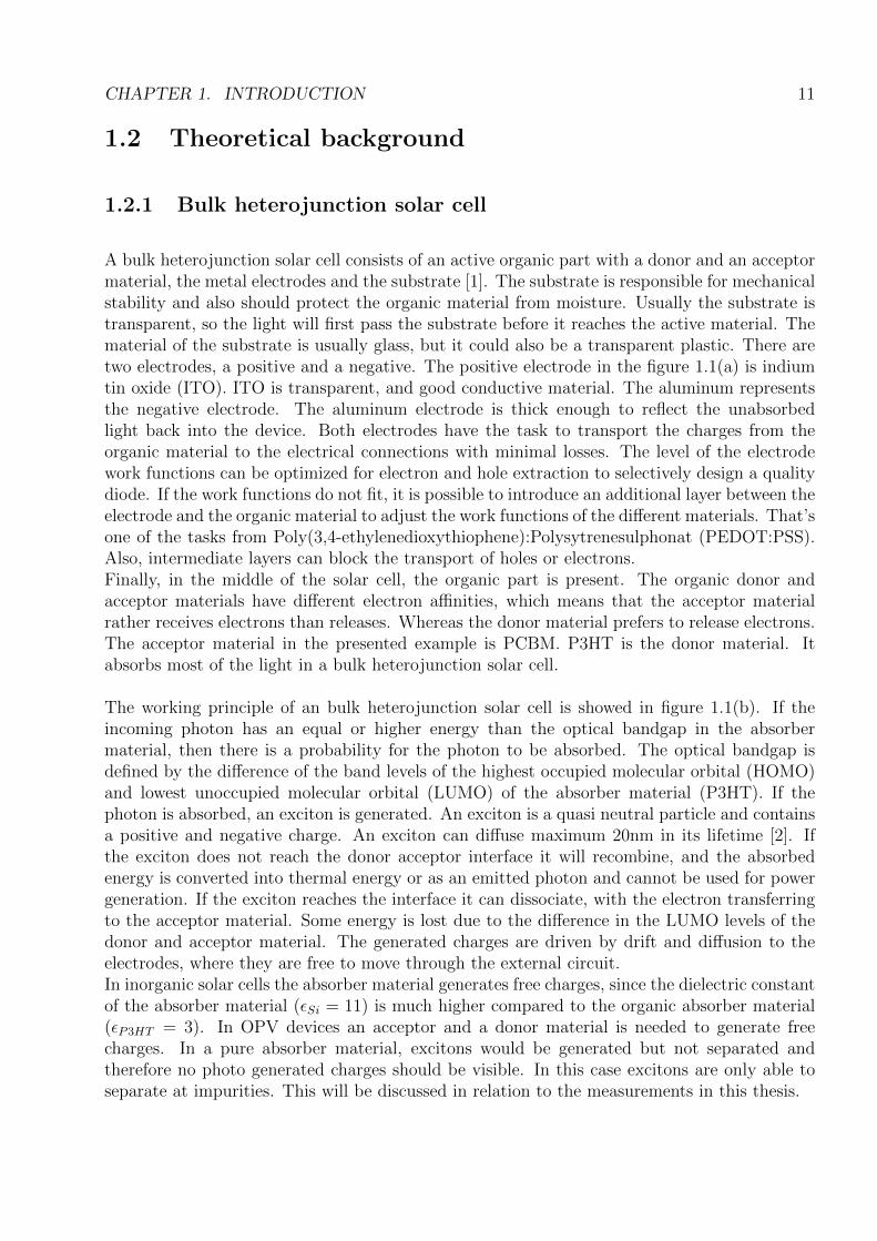
A bulk heterojunction solar cell consists of an active organic part with a donor and an acceptormaterial, the metal electrodes and the substrate [1]. The substrate is responsible for mechanicalstability and also should protect the organic material from moisture. Usually the substrate istransparent, so the light will first pass the substrate before it reaches the active material. Thematerial of the substrate is usually glass, but it could also be a transparent plastic. There aretwo electrodes, a positive and a negative. The positive electrode in the figure 1.1(a) is indiumtin oxide (ITO). ITO is transparent, and good conductive material. The aluminum representsthe negative electrode. The aluminum electrode is thick enough to reflect the unabsorbedlight back into the device. Both electrodes have the task to transport the charges from theorganic material to the electrical connections with minimal losses. The level of the electrodework functions can be optimized for electron and hole extraction to selectively design a qualitydiode. If the work functions do not fit, it is possible to introduce an additional layer between theelectrode and the organic material to adjust the work functions of the different materials. That’sone of the tasks from Poly(3,4-ethylenedioxythiophene):Polysytrenesulphonat (PEDOT:PSS).Also, intermediate layers can block the transport of holes or electrons.Finally, in the middle of the solar cell, the organic part is present. The organic donor andacceptor materials have different electron affinities, which means that the acceptor materialrather receives electrons than releases. Whereas the donor material prefers to release electrons.The acceptor material in the presented example is PCBM. P3HT is the donor material. Itabsorbs most of the light in a bulk heterojunction solar cell.
The working principle of an bulk heterojunction solar cell is showed in figure 1.1(b). If theincoming photon has an equal or higher energy than the optical bandgap in the absorbermaterial, then there is a probability for the photon to be absorbed. The optical bandgap isdefined by the difference of the band levels of the highest occupied molecular orbital (HOMO)and lowest unoccupied molecular orbital (LUMO) of the absorber material (P3HT). If thephoton is absorbed, an exciton is generated. An exciton is a quasi neutral particle and containsa positive and negative charge. An exciton can diffuse maximum 20nm in its lifetime [2]. Ifthe exciton does not reach the donor acceptor interface it will recombine, and the absorbedenergy is converted into thermal energy or as an emitted photon and cannot be used for powergeneration. If the exciton reaches the interface it can dissociate, with the electron transferringto the acceptor material. Some energy is lost due to the difference in the LUMO levels of thedonor and acceptor material. The generated charges are driven by drift and diffusion to theelectrodes, where they are free to move through the external circuit.In inorganic solar cells the absorber material generates free charges, since the dielectric constantof the absorber material (εSi = 11) is much higher compared to the organic absorber material(εP3HT = 3). In OPV devices an acceptor and a donor material is needed to generate freecharges. In a pure absorber material, excitons would be generated but not separated andtherefore no photo generated charges should be visible. In this case excitons are only able toseparate at impurities. This will be discussed in relation to the measurements in this thesis.

CHAPTER 1. INTRODUCTION 12
GLAS
ITOPEDOT:PSS
P3HT / PCBM
ALU
Light
V
1.
2.
3.
5.
5.
4b.
(a) (b)
4a.
Figure 1.1: a) Intersection of a bulk heterojunction solar cell. b) Concept of the functionality of an organic solarcell: 1.Light with energy E = hν, 2.Exciton generation, 3.Exciton diffusion, 4a.Exciton dissociation, 4b.Excitonrecombination, 5.Charge drift and diffusion to specific electrodes
According to the diffusion length of about 20 nm, the donor and acceptor material shouldinterpenetrate each other in the nanometer scale, to keep a low probability for the recombinationof the exciton. The separated charges also have a lifetime. If the thickness of the film is toohigh, the charges will recombine before they reach the electrodes. Therefore, the thicknessof the device is limited by the mobility of the carriers in the organic semiconductor. In thindevices, on the other hand, many photons are not absorbed. Thus, there is a optimum to find,between high absorption rate and low recombination rate for separated charges. The systemcan be optimized by increasing the carrier mobility [3] and the optical absorption coefficient ofthe materials.
1.2.2 Space charge limited current
With the space charge limited current (SCLC) method, one can calculate the mobility of aorganic semiconductor with a simple IV curve. The SCLC is a description of a behavior of thevoltage dependence on the current in a semiconductor. SCLC occurs when the charge carrierconcentration is larger than the doping level or the free carriers in a semiconductor. This canhappen by injecting charge carriers into the device. This current is dominated by the appliedfield, what one calls a drift current. The high charge carrier concentration affects the electricfield distribution, which makes a feedback loop between the field and the current. This feedbackmechanism is described in the relation 1.1 and is called the Mott-Gurney law.
J =9εsµV
2
8L3(1.1)

CHAPTER 1. INTRODUCTION 13
V is the applied voltage, J the SCLC, L is the thickness of the film, µ the mobility and εs is thepermittivity of the semiconductor. It has been shown that SCLC can also be used for mobilitymeasurement of organic diodes [4]. It is under discussion, that the mobility µ depends on theelectric field [5], which is not considered in the Mott-Gurney law. In this thesis the originalMott-Gurney law will be used for comparison to the other techniques.
1.2.3 4 wire conductivity
A modified 4 wire conductivity measurement technique is used in this thesis to measure theconductivity of a thin film. Here the standard 4 wire technique will be introduced.
In order to measure a device accurately, it is important to make sure that the measured physicalproperties are independent of the used setup. The simplest way to measure the resistance (R) ofa device is with 2 contacting wires. By sourcing a current (I) one can measure the voltage (V ).After Ohms law R = V
Ithe resistance can be calculated. 2 wire conductivity measurements
can be accurate, but there are some issues.
V
A
R2
R5
R1
R3
R4
Figure 1.2: Electrical equivalent circuit of a 4 wire conductivity measurement
Figure 1.2 shows an equivalent circuit diagram of a 4 wire setup. R1 represents the resistanceof interest. R2 and R5 includes the resistances of the cables to the current source A and thecontact resistances from the wire to the devices. R3 and R4 refer also to the resistances of thecontacts to the device and the cables to the voltage meter. In order to measure the resistanceR1, the power supply (A) should regulate the sourced current accurately. This would makethe voltage over the device independently of R2 and R5. To measure to voltage drop over R1independently of R3 and R4, the internal resistance of the voltage meter (V ) should be infinite.In practice one can choose a voltage meter with a very high internal resistance or at least muchhigher than R1. With this configuration the calculated value of R1 is almost independent ofR2−R5, which is the purpose and advantage of the 4 wire conductivity measurement.
CHAPTER 1. INTRODUCTION 14
1
ρ= σ = enµ (1.2)
In equation 1.2 it is shown, that the reciprocal value from the resistivity (ρ) is the conductivity(σ). The conductivity depends on the charge carrier concentration (n) and on the mobility(µ) of charge carriers itself. By measuring σ, n and µ the consistency of the used measurementmethods can be proven, since e is the elementary charge and thus constant.
1.2.4 Impedance measurements
The impedance of a device can be investigated by applying a small signal AC voltage in additionto a DC bias. This allows for the full, frequency dependent, characterization of the resistances,capacitances and inductances that may be acting within the device.A resistance does not depend on the applied frequency. If a device does have a capacitive orinductive behavior the measured impedance depends on the applied frequency of the voltage.This dependence is readable in the phase shift between the voltage and the current signal.Mathematically this additional information is included in a complex number, which is theimpedance (Z). In formula 1.3 θ is the angle between voltage and current signal. R is the realpart of the complex number and the resistance, X the reactance, and V and I here also referto voltage and current but in a complex number.
Z = |Z|ejθ = R + jX =V
I(1.3)
Zc =1
jωC(1.4)
Formula 1.4 reflects the impedance of an ideal capacitor. Where ω = 2πf is the angularfrequency of the alternating current and C the capacitance. The advantage of the complexnumbers are, Ohms and Kirchhoffs law can also be used, not only in direct current (DC),but also in alternating current (AC).
Measuring the impedance is typically done frequency dependent, and is then called impedancespectroscopy. But it can also be done at different bias voltages. This means, one applies aDC offset on the device and modulate on the bias a small alternating voltage, which gives theinformation of the impedance at a specific bias (or offset) voltage. In this thesis diodes will bemeasured. Diodes have non linear IV characteristic and it is possible to interpret and find outdifferent physical parameters by varying the frequency or bias of the applied voltage.
1.2.4.1 Impedance spectroscopy
As mentioned, in impedance spectroscopy the impedance is measured at various frequencies.The interpretation of the measured results can be done in different ways. Here we interpret

CHAPTER 1. INTRODUCTION 15
the results by fitting the measured values with a theoretical equivalent circuit. This circuit cancontain resistors and capacitors. It has to be mentioned, that infinite equivalent models canreflect the same impedance behavior. To interpret the measured results it makes sense that theequivalent circuit model has components with a physical meaning to the the device under test.
Rp
Rs
Cp
Re(Z)
-Im(Z)
(a) (b)
RsRp
ω
Figure 1.3: (a) example for an equivalent curcuit. (b) Nyquist diagram of the equivalent circuit
In figure 1.3(a) an equivalent circuit diagram is shown with a series resistor (Rs), parallelresistor (Rp) and a parallel capacitor (Cp). The impedance spectrum of this circuit is shown infigure 1.3(b), as the so called Nyquist diagram, where the x axis is the real part and the y axisis the imaginary part of the complex impedance. One can read out of this diagram that dueto the negative half circle, there is one capacitor in the circuit with a parallel resistor with thevalue Rp. Since there is a gap between the half circle and the imaginary axis, a series resistor(Rs) which has the size of the gap is present as well. ω is the angular frequency and increasesfrom the right to the left.
1.2.4.2 Mott Schottky plot
A semiconductor has a charge carrier concentration which effects the distribution of the electricfields within the device. If the carrier concentration is within a certain range, then a Schottkycontact is formed at a metal-semiconductor interface and a built-in potential is present. Both,the charge carrier concentration (N) and the built-in potential (ψbi) at a Schottky contact canbe measured and calculated. The used theory will be introduced here.
A Schottky contact consist of a metal and a semiconductor. The Fermi level (EF in figure1.4(a)) of a p-type semiconductor is lower than the Fermi level of the metal in a Schottkydiode. Which means, that the electron energy level with a occupation probability of 50 % ina p-type semiconductor is lower than in the metal. In order to get a Schottky contact with a

CHAPTER 1. INTRODUCTION 16
n-type semiconductor, the Fermi level of a n-type semiconductor is higher than the Fermi levelof the metal. eφm in figure 1.4(a) stays for the workfunction of the metal and is the differencebetween the Fermi level of the metal and the vacuum level. eψi refers to ionization energy andeφp refers to the difference of the valence band (EV ) and the Fermi level of the semiconductor.e is the elementary charge.
(a) (b)
Evac
eΦm
eΦp
EC
EFEV eΨbi
EC
EFEV
W
p typeregion
metallicregion
eΨi
Figure 1.4: Energy band diagram of a p-type Schottky contact. Metal and semiconductor in separated system(a) and in connected system (b).
If there is a contact between the metal and the semiconductor, charges will move across theinterface to provide an equilibrium uniform Fermi Level (figure 1.4(b)). In the semiconductorregion close to the contact are no mobile charges anymore. This region is called depletionlayer and has the width W . This system of a semiconductor and a metal in contact is called aSchottky contact and acts like a diode. By applying a positive voltage on the semiconductorside the depletion layer gets smaller and the current gets higher, this is the so called forwardbias. By applying a negative voltage the depletion layer gets bigger, and the current getssmaller, which means, the diode works in the reverse bias regime. The potential differencebetween the Fermi levels is the contact potential or built-in potential ψbi = ψi − φm − φp. Thedepletion layer width (W ) is defined by equation 1.5 [6]:
W =
√√√√2εseN
(Ψbi − V −
kT
e
)(1.5)
• εs: Permittivity of the semiconductor
• V : Applied potential or voltage
• kTe
: Correction factor for majority-carrier distribution tails [7].
• k: Boltzmann constant
• N : Charge carrier concentration in the semiconductor

CHAPTER 1. INTRODUCTION 17
In the following we take a look to the electric field and charge carrier distribution in the film.The material we use in this thesis are organic materials, which do not have to be doped,because the conduction bands or LUMO levels are different in the p-type (donor) and n-type(acceptor) semiconductors, whereby the charge separation is forced. With the assumption, thatthe intrinsic charges are distributed uniformly, the charge carrier concentration N is constant,see 1.5(a). Based on the Poisson equation 1.6, the integration of the charge carrier concentrationgives the electric field (1.5(b)) and the integration of the electric field gives the potential overthe film thickness (1.5(c)).
− d2ψ(x)
dx2=dE(x)
dx=N(x)
εs(1.6)
• ψ: Potential
• E: Electric field
• x: Distance perpendicular to the substrate
• N : Charge carrier density
(a)
NA
W
x
charge density
(b)
W
x
electricfield
p typeregion
metallicregion
(c)
Ψbi
W
x
Ψ
00
Figure 1.5: Ideal Schottky contact with a depletion layer thickness W , (a) space-charge distribution, (b) electric-field distribution, (c) potential distribution where ψbi is the built-in potential.
This potential can be used to derive the energy bands (1.4(b)). The derivation for the depletionlayer thickness is based on the Poisson equation. In a Schottky diode the metal has a very highcharge carrier concentration, and thus one can imagine that the depletion width is very small,almost zero and has not to be considered. However, the depletion layer calculations refer tothe semiconductor.
The capacitance (C) can be measured by impedance with various bias voltages. C is calculatedfrom the impedance by an equivalent circuit model with a capacitor and a parallel resistor.
C−2 =2(ψbi − V )
A2eεε0N(1.7)
V is the applied bias voltage and A the area of the capacitor. A series resistance is usuallynot taken into account, but if one measures Mott Schottky plot at frequencies higher than 100kHz, corrections need to bee made [8]. Measuring the capacitance over bias voltages showed

CHAPTER 1. INTRODUCTION 18
in C−2 plot gives a straight line, which is a good indication for a present Schottky contact [9].The extrapolated intersection with the bias axis gives the built-in potential (ψbi), whereas theslope of the line gives the charge carrier concentration with equation 1.8 which is derived from1.7.
N = − 2
A2eεε0 · slope(1.8)
1.2.5 CELIV
Charge extraction by linear increasing voltage (CELIV) is a method to measure charge carrierconcentration (N), conductivity (σ) and mobility (µ) [10]. The method can be used for highand low conductive semiconductors. The idea is to apply a linear increasing voltage (V ) onthe reverse connected device and measure the current response over the time by an oscilloscope(see figure 1.6).
GLAS
ITOPEDOT:PSS
P3HT / PCBM
ALU
Light/Laser
Oscilloscope
(a)
I
Function generator
V
tA
Vmax
Vofftdel tpulseLightpulse
I
t
tmax
j(0)
ΔjQe
(b)
Figure 1.6: CELIV measurement setup. In picture (a): connection diagram. The device is connected in reversedirection to run the diode in reverse bias. (b): the function generator creates the voltage ramp (A) and theoscilloscope measures the current response.
The device needs to have a blocking contact (for example a Schottky contact), otherwise chargesare injected and the current pulse is affected or even not visible anymore. If the active organicmaterial would have no free charge carriers, the current response would look rectangular withthe height j(0) = C
Vmax−Vofftpulse
, which represents a capacitive behavior with the geometric capac-
itance (C) from the diode. Free charges in the active layer begin to move, due to the increasingelectric field and are finally extracted at the electrodes. The extracted charges are responsiblefor the additional peak on j(0), while the time tmax gives information about mobility µ (seeequation 1.9) of the extracted charges. d is the thickness of the film and Qe represents the totalamount of extracted charges which is the dashed area in figure 1.6(b). With the volume of thefilm, the charge carrier concentration can be determined.
CHAPTER 1. INTRODUCTION 19
With formula 1.9 one can calculate the mobility. This formula is valid at low light intensitiesand with uniformly photo generated charge carriers, which means, an absorption dependencewithin the film thickness is not considered. Also, equation (1.9) is based on the drift current.A possible diffusion current, specially under illumination, is not considered.
µ =2d2
3At2max
[1 + 0.36 ∆j
j(0)
] (1.9)
The determination of conductivity directly by CELIV will not be used in this thesis.
Chapter 2
Experimental details
2.1 Devices
This chapter introduces the used materials and shows the production procedure of the measureddevices.
2.1.1 Materials
2.1.1.1 P3HT
Poly(3-hexylthiophene-2,5-diyl) (P3HT) is a conjugated polymer, see figure 2.1. It is a com-monly used polymer in organic solar cells and acts as the light absorbing and hole transportingmaterial. P3HT has a high solubility and due to the alkyl-groups a high potential crystallinity.The degree of crystallinity is affected by the regioregularity of the polymer. A regioregularP3HT usually has a regioregularity of minimum 90 %. The higher the regioregularity, thehigher the cristallinity. It was also recognized that higher molecular weight leads to a red shiftin the absorbtion spectrum and to higher hole mobility [11][12].
P3HT is a conjugated polymer with a thiophene backbone. The carbon atoms in the thiophenerings are sp2 hybridized, and thus form a π-bond with the neighbor carbon atoms. In thepolymer the π-bonds form a π-band which is called the highest occupied molecular orbital(HOMO). In this π-band the electrons are delocalized. The bandgap of thiophenes is build bytransition from the aromatic into the quinoid structure. Impurities in the polymer act like ap-type doping and are giving pure P3HT a electrical conductivity.
The used P3HT is from Rieke: 4002-E and has a regioregularity of at least 90 %. The averagemolecular weight is 50000 g/mol. The LUMO level is 3.2 eV and the HOMO level is at
20

CHAPTER 2. EXPERIMENTAL DETAILS 21
Figure 2.1: Organic molecules used in solar cells: Regioregular P3HT, PCBM, PEDOT:PSS
5.1 eV [13]. The hole mobility in P3HT depends on different factors and lies between 10−5 and10−2 cm2/V s [5][2]. The electron mobility is negligible small [3].
2.1.1.2 PCBM
Phenyl-C61-butyric acid methyl ester (PCBM) is a fullerene based molecule (figure 2.1). Itcontains a Bucky-ball (C60), and to make it soluble the methyl-ester group is attached. PCBMis a n-type material and can take up to six electrons. It also has a π-band, but the electronsare moving in the π∗-band, or LUMO. The mobility in PCBM is between 2 · 10−3 and 2 · 10−2
cm2/V s [3]. The hole mobility is negligible small. The HOMO level is 6.1 eV and the LUMOlevel is 4.4 eV [13].In this thesis the PCBM from Solenne 99 % is used.
2.1.1.3 ITO
Indium tin oxide (ITO) is a transparent conductive oxide. In an organic solar cell at leastone electrode has to be transparent in order to absorb the light in the active layer. It is quitecommon in opto-electronics to use ITO. In this thesis the ITO was bought already on the glassfrom Kintec. It has a sheet resistance of 15 Ω/sq. The work function is 4.9 eV.
2.1.1.4 PEDOT:PSS
Poly(3, 4 − ethylenedioxythiophene) : Polysytrenesulphonat (PEDOT:PSS) is a conductingconjugated polymer (figure 2.1). PEDOT:PSS is used to improve the extraction propertiesbetween the ITO and the P3HT and to smooth out the ITO film. The layer thickness is usuallyless than 100 nm and thus transparent. In this thesis the PEDOT:PSS VP AI 4083 fromCLEVIOS is used, which has a work function of 4.8-5.2 eV [14]. The resistivity lies between500− 5000 Ωcm.

CHAPTER 2. EXPERIMENTAL DETAILS 22
2.1.2 Production procedure
The solar cell and the P3HT diode are produced with following procedure. Deviations to theprocedure are mentioned in text of the specific devices.
The first step is to cut the glass. Usually the devices at LIOS (Linz Institute for Organic SolarCells) have a size of about 14 mm x 14 mm x 1 mm. The ITO has to be etched in the areaof the aluminum contacts. Therefore the rest of the device has to be protected by a tape.The etching process with a 37 % concentrated HCL (hydrochloric acid) solution takes 5minby an ITO thickness of 150 nm, and the HCL can be reused several times. The next step isto clean the glass. The cleaning process was done in a ultrasonic bath in acetone for 10minand in isopropanol for 10 min. Now the layers can be spin coated on the device. First thePEDOT:PSS is filtered by a PES membrane with 0.45 µm pores and then spin coated twiceby a speed of 4000 rpm for 40 s. After removal the PEDOT:PSS with distilled water from thecontact areas (figure 2.2(a)) the device has to be annealed at 120 C for 10 min to remove theresidual water in the film.
(a) (b) (c)
Figure 2.2: Production steps of a device. (a) Spin coat PEDOT:PSS on etched ITO(yellow). (b) Spin coatorganic material and remove the edges. (c) Evaporate aluminum electrodes
The organic material for a solar cell contains a mix of PCBM and P3HT. This materials aredissolved in chlorobenzene. The solution concentration lies between 10 and 30 mg/ml. Thesolutions in this thesis are made with 30 mg/ml, and the mixing ratio between PCBM andP3HT was made 1:1. In order to get a good solution, the mix should be stirred with a stir barfor at least 1h. Now the organic material can be spin coated with a speed between 800 rpmand 1500 rpm. The devices in this thesis are spin coated with 800 rpm. The organic materialat the contacts has to be removed as well. This can be done with acetone, toluol or it can bescratched off with a sharp knife. A sharp knife is usually used when the spin coat process wasdone in the glovebox. In this thesis the organic films are spin coated in the glovebox. Now thealuminum electrodes with a thickness of 100 nm are evaporated. Specially in a solar cell it isimportant to make a last annealing step to improve the degree of crystallinity in the organicfilm. The annealing step is done at 120 C for 10 min. The device is finished (figure 2.2(c)).

CHAPTER 2. EXPERIMENTAL DETAILS 23
2.1.3 P3HT device
GLA
SS
- 1mm
ITO
- 150nmP
ED
OT
:PS
S - 40nm
P3H
T - 230nm
ALU
- 100nm
Light
Energy bandsin the used materials
4.9 eV5.2 eV
3.2 eV
4.2 eV
5.1 eV
Evac
Energy banddiagram of device
Figure 2.3: Thickness, work functions, electron affinity and energy band diagram of the P3HT device
The device for measurements with pure P3HT is shown in figure 2.3. As a general understand-ing, PEDOT:PSS on ITO forms an ohmic contact with the P3HT, whereas the P3HT formsa Schottky contact with aluminum and thus has a depletion layer [15]. The energy bands inthe P3HT layer show a dotted line, which refers to the p-type doping level. The dotted linein the energy band diagram represents the Fermi level. The thicknesses of the different layers,measured with an atomic force microscope (AFM) are also shown. The active area of the diodeis roughly 0.1 cm2, and measured for each individual device. The production steps of the deviceare documented in chapter 2.1.2. In this device no final annealing step was made.
2.1.4 P3HT:PCBM bulk-heterojunction device
Here the BHJ SC is introduced. The active film consists of an intermixing P3HT and PCBMbulk, which will be measured with the different techniques.

CHAPTER 2. EXPERIMENTAL DETAILS 24
GLA
SS
- 1mm
ITO
- 150nmP
ED
OT
:PS
S - 40nm
P3H
T/ P
CB
M - 160nm
ALU
- 100nm
Light
4.9 eV5.2 eV
3.2 eV
4.2 eV
5.1 eV
Evac
4.4 eV
6.1 eV
Energy bandsin the used materials
Figure 2.4: Thickness, work functions and electron affinities of an organic solar cell.
In figure 2.4, we see the thicknesses of the films and there work functions respectively electronaffinities. The active area is 0.11 cm2 and has a thickness of 160 nm. The concept of the BHJsolar cell is introduced in chapter 1.2.1. This device was spin coated outside the glovebox.
2.1.5 P3HT device for conductivity measurements
To measure the conductivity in low conductive materials, like P3HT, a new technique is intro-duced in this section. The device is designed to, not only measure the conductivity, but alsothe mobility and charge carrier concentration at equal temperature and degradation conditions.With equation σ = enµ the relation between conductivity(σ), mobility(µ) and charge carrierconcentration(n) is defined. Each parameter will be measured by itself and should complementeach other. In this chapter the device is introduced to measure the mobility by CELIV, thecharge carrier concentration by impedance and the conductivity by a modified 4 wire conductiv-ity measurement. This measurements are done in the cryostat (figure 2.11), in order to controlthe temperature accurately and to prevent any doping by oxygen, since the cryostat works invacuum.

CHAPTER 2. EXPERIMENTAL DETAILS 25
0.5mm
6mmITO
PEDOT:PSS
ITO
(a) Top view
(c) Zoom & intersection through the device
(b) 3D view
Glass - 1mm
ITO - 150nm
Organic layer - 320nm
Aluminum - 100nm
PEDOT:PSS - 40nm
0.5mm
I
V
Device for impedance and CELIV measurements
Device for modified 4 wire measurement
Figure 2.5: Device assembly for impedance, CELIV and modified 4 wire conductivity measurements. (a) Devicewithout organic film and without electrodes. (b) Final device with a diode and a resistance for the modified4 wire conductivity measurement. (c) Intersection of layers for modified 4 wire conductivity measurement andthe connection diagram
To measure mobility, charge carrier concentration and conductivity a device with a special ITOshape is used. In figure 2.5(a) the ITO and the PEDOT:PSS on the glass substrate is shown.The gap of 0.5 mm is used to measure the voltage drop over the organic layer with a modified4 wire measurement technique. The device for impedance and CELIV measurements is anorganic diode between the aluminum and ITO layer. In picture 2.5(c) the connection diagramfor the modified 4 wire conductivity measurement by a zoom of the intersection is shown, wherethe current is sourced on the top aluminum contacts and the voltage is measured at the ITOcontacts. The conductivity of the ITO contacts are much higher than from the measured P3HT.Thus, the voltage drop from the measured material in the gap of 0.5 mm is measured. Withthe intersection area (A = filmthickness · gapwidth(6mm)), the length (l = 0.5 mm) of thegap and the measured resistance (R = V/I) over the gap, the conductivity can be measuredby equation 2.1.
σ =l
R · A(2.1)
For example, with a measured resistance of 1 GΩ and a film thickness of 200 nm the conductivitywould be 4.16 ·10−6Ω−1cm−1.A contact resistance between the ITO and the measured material, for example P3HT, is notconsidered. Since P3HT and ITO makes a quasi ohmic contact and the measured resistance isin the Giga ohm regime, the contact resistance between ITO and the measured material shouldnot affect the measured resistance significantly.
Mobility, charge carrier concentration and conductivity are geometry independent values, thus
CHAPTER 2. EXPERIMENTAL DETAILS 26
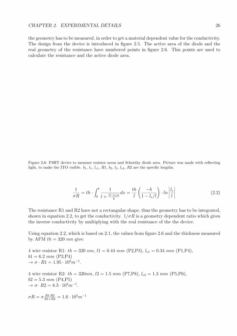
the geometry has to be measured, in order to get a material dependent value for the conductivity.The design from the device is introduced in figure 2.5. The active area of the diode and thereal geometry of the resistance have numbered points in figure 2.6. This points are used tocalculate the resistance and the active diode area.
Figure 2.6: P3HT device to measure resistor areas and Schottky diode area. Picture was made with reflectinglight, to make the ITO visible. b1, l1, le1, R1, b2, l2, le2, R2 are the specific lengths.
1
σR= th ·
∫ b
0
1
l + (l−le)xb
dx =th
l
(−b
1− le/l
)· ln
∣∣∣∣∣ lel∣∣∣∣∣ (2.2)
The resistance R1 and R2 have not a rectangular shape, thus the geometry has to be integrated,shown in equation 2.2, to get the conductivity. 1/σR is a geometry dependent ratio which givesthe inverse conductivity by multiplying with the real resistance of the the device.
Using equation 2.2, which is based on 2.1, the values from figure 2.6 and the thickness measuredby AFM th = 320 nm give:
4 wire resistor R1: th = 320 nm, l1 = 0.44 mm (P2,P3), le1 = 0.34 mm (P1,P4),b1 = 6.2 mm (P3,P4)→ σ ·R1 = 1.95 · 105m−1.
4 wire resistor R2: th = 320nm, l2 = 1.5 mm (P7,P8), le2 = 1.3 mm (P5,P6),b2 = 5.3 mm (P4,P5)→ σ· R2 = 8.3 · 105m−1.
σR = σ R1·R2R1+R2
= 1.6 · 105m−1

CHAPTER 2. EXPERIMENTAL DETAILS 27
With the factor σR, measuring the resistance R gives thus the conductivity of the material.The area of the Schottky diode is defined by points 10-13 (figure 2.6) and is = 0.1 cm2.
2.1.6 P3HT:PCBM bulk-heterojunction device for conductivity mea-surements
The layout of the solar cell device is almost the same as the layout used in the P3HT device inlast chapter. In this device no parallel resistors are needed to calculate the conductivity by 4wire technique, because the bulk does is not touch the horizontal electrode and therefore notsignificantly contribute to the measured resistance.
y
x
1 2
34
5
6
7
89
10
11
12
Sch
ottk
y -
diod
e
4 w
ire r
esis
tanc
e
Figure 2.7: Picture of solar cell device. The picture was taken with reflecting light, to make the ITO layervisible. The active area of the Schottky-diode and the 4 wire resistor are shown with there coordinates in x andy axis.
Using equation 2.2, the values from figure 2.7 and the thickness measured by AFM th = 220nm give:
4 wire resistor: th = 220 nm, l = 0.55mm(P1, P2), le = 0.47mm(P3, P4), b1 = 5.7mm(P2, P3)→ σ ·R = 4.03 · 105m−1.
The area of the Schottky diode is defined by points 5-12 (figure 2.7) and is = 0.13 cm2.
CHAPTER 2. EXPERIMENTAL DETAILS 28
2.2 Equipment
In this chapter the used equipment is introduced. Chambers are needed to prevent variationsin the measured quantities due to oxygen exposure. Either the chamber can be filled withnitrogen or argon (small chamber), or the chamber has to be evacuated (cryostat).
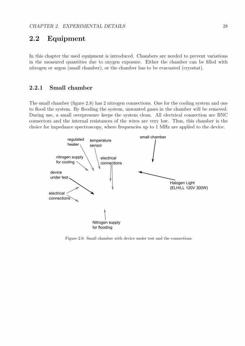
2.2.1 Small chamber
The small chamber (figure 2.8) has 2 nitrogen connections. One for the cooling system and oneto flood the system. By flooding the system, unwanted gases in the chamber will be removed.During use, a small overpressure keeps the system clean. All electrical connection are BNCconnectors and the internal resistances of the wires are very low. Thus, this chamber is thechoice for impedance spectroscopy, where frequencies up to 1 MHz are applied to the device.
device under test
small chamber
Halogen Light(ELH/LL 120V 300W)
electrical connections
electrical connections
nitrogen supplyfor cooling
temperature sensor
regulatedheater
Nitrogen supplyfor flooding
Figure 2.8: Small chamber with device under test and the connections
CHAPTER 2. EXPERIMENTAL DETAILS 29
Impedance or CELIV equipment
HighLow
Chamber filled with N2
Multimeter Fluke 289
Temp Current
Si photodiodeHamamatsu S1787
Thermo-coupleTyp K
Halogen Light Bulb/ divine lighting ELH/LL 120V 300W
device under test
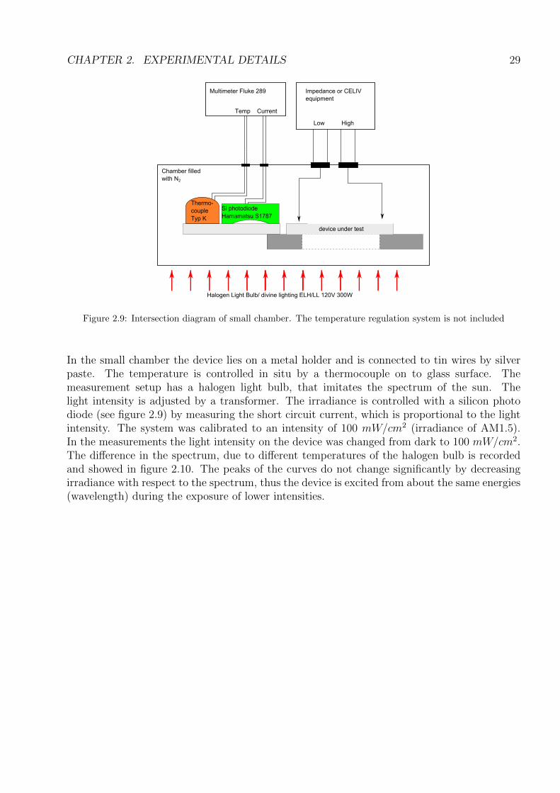
Figure 2.9: Intersection diagram of small chamber. The temperature regulation system is not included
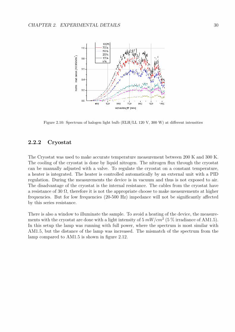
In the small chamber the device lies on a metal holder and is connected to tin wires by silverpaste. The temperature is controlled in situ by a thermocouple on to glass surface. Themeasurement setup has a halogen light bulb, that imitates the spectrum of the sun. Thelight intensity is adjusted by a transformer. The irradiance is controlled with a silicon photodiode (see figure 2.9) by measuring the short circuit current, which is proportional to the lightintensity. The system was calibrated to an intensity of 100 mW/cm2 (irradiance of AM1.5).In the measurements the light intensity on the device was changed from dark to 100 mW/cm2.The difference in the spectrum, due to different temperatures of the halogen bulb is recordedand showed in figure 2.10. The peaks of the curves do not change significantly by decreasingirradiance with respect to the spectrum, thus the device is excited from about the same energies(wavelength) during the exposure of lower intensities.
CHAPTER 2. EXPERIMENTAL DETAILS 30
Figure 2.10: Spectrum of halogen light bulb (ELH/LL 120 V, 300 W) at different intensities
2.2.2 Cryostat
The Cryostat was used to make accurate temperature measurement between 200 K and 300 K.The cooling of the cryostat is done by liquid nitrogen. The nitrogen flux through the cryostatcan be manually adjusted with a valve. To regulate the cryostat on a constant temperature,a heater is integrated. The heater is controlled automatically by an external unit with a PIDregulation. During the measurements the device is in vacuum and thus is not exposed to air.The disadvantage of the cryostat is the internal resistance. The cables from the cryostat havea resistance of 30 Ω, therefore it is not the appropriate choose to make measurements at higherfrequencies. But for low frequencies (20-500 Hz) impedance will not be significantly affectedby this series resistance.
There is also a window to illuminate the sample. To avoid a heating of the device, the measure-ments with the cryostat are done with a light intensity of 5 mW/cm2 (5 % irradiance of AM1.5).In this setup the lamp was running with full power, where the spectrum is most similar withAM1.5, but the distance of the lamp was increased. The mismatch of the spectrum from thelamp compared to AM1.5 is shown in figure 2.12.

CHAPTER 2. EXPERIMENTAL DETAILS 31
Window for deviceillumination
Electrical connection
Vacuumconnection
Si reference photodiode
Cryostat
Inlet for liquidNitrogen
Shutter to protect thedevice from unwanted irradiance
Connections for temperature control
Valve to adjust the nitrogen flow
Figure 2.11: Cryostat and his connections
Figure 2.12: Spectrum of halogen lamp ELH 120V and from AM1.5
2.2.3 Apparatus
The vacuum pump is connected to the cryostat and it achieves a vacuum of about 4 ·10−5 mbar.The cryostat is not directly visible in figure 2.13. The device in the cryostat is illuminated fromthe Halogen light bulb. The distance from the light source to the device in figure 2.13 is

CHAPTER 2. EXPERIMENTAL DETAILS 32
Source Measure UnitKeithley 236
Labview forimpedance measurements
CryostatOxford instrumentOptistat DNV
LCR MeterHP 4284A
ElectrometerKeithley 6514
Halogen light bulbELH 120V
Labview forCELIV measurements
OscilloscopeTektronixTDS 754C
Trans-former0-230V
Pulse generatorStanford Research SystemsDG535
Function generatorAgilent 33250A
MultimeterFluke 289
Temperatur control Oxford instrumentITC 502S
Pfeiffer vacuumpumpDCU
Figure 2.13: Test equipment for impedance, CELIV and 4 wire conductivity measurements
adjusted to have 5 mW/cm2 intensity on the device, this is controlled by a reference silicondiode. The temperature control unit regulates the current from the heater in the cryostat, andreads the information from the temperature sensor in the cryostat to regulate a user definedtemperature. For impedance measurements the LCR meter is used. The LCR meter worksin 4 wire mode and is directly connected to the cryostat. An external LabView program canbe used to define a measurement procedure. The program was defined to make measurementsbetween 20 Hz and 1 MHz and between -2 V and +2 V.
The CELIV setup is connected like in figure 1.6. The function generator, which is triggeredby the pulse generator, applies a positive ramp on the negative connection from the device(aluminum electrode). The positive connection of the device (ITO electrode) is connected tothe oscilloscope. The internal resistance of 50 Ω works as a shunt. Thus, the oscilloscopeshows a voltage which is proportional to the current through the device. Both, the functiongenerator and the oscilloscope are grounded, this is where to current flows back to the functiongenerator. Additionally there is a laser system (Continuum Surelite OPO Plus 355 nm). Thelaser is pointing on the device. The pulse generator controls the timing to the laser and to thefunction generator. All pieces of equipment are connected over GPIB to the LabView software,from where all necessary parameters can be adjusted.

CHAPTER 2. EXPERIMENTAL DETAILS 33
For the modified 4 wire conductivity measurements, the current is sourced by the Keithley236 (see figure 2.13). To use the Keithley 236 was necessary, because of sourcing in the nanoampere range, since the film resistance is in the giga ohm range. To measure the voltage drop, aVoltage meter with a very high internal resistance is needed. An electrometer like the Keithley6514 with an almost infinite resistance was used.
The Keithley 236 was also used to measure the IV characteristics of the device, here one appliesdifferent voltages on the device and measures the current response.
Chapter 3
Behavior of pure P3HT films
In this chapter a pure P3HT film (see 2.1.1.1) will be investigated with different measurementtechniques.
3.1 IV behavior of P3HT films
In this section IV measurements with the Schottky device, introduced in section 2.1.3, measuredin the small chamber (2.2.1) are shown.In according to Campbell [16], the Trap-Free-Space-Charge-Limited-Current (TFSCLC) theoryin organic materials can be used, if the hole injection electrode ITO is treated by either a plasmaor by a PEDOT:PSS layer, as in this device. Organic diodes show an ohmic behavior at a lowpositive voltage, and a SCLC behavior at higher positive voltage. Here we use the Mott-Gurneylaw (equation 1.1), where the temperature and E-field dependence of the mobility is not takeninto account.
34
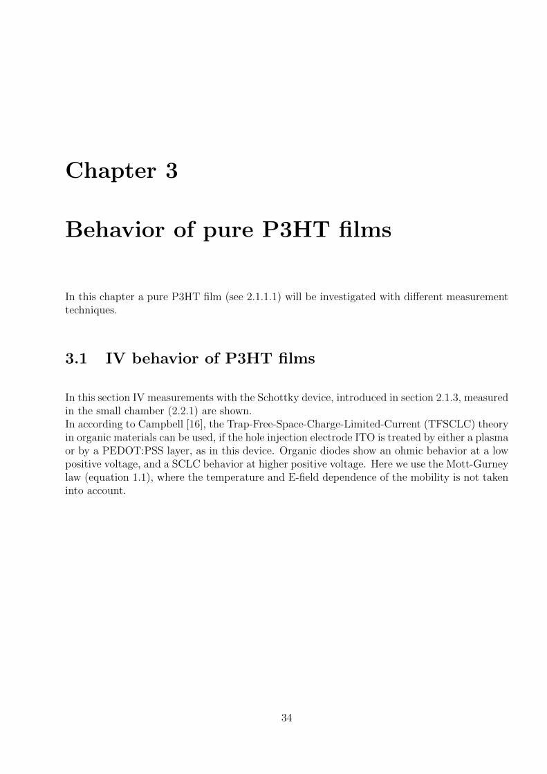
CHAPTER 3. BEHAVIOR OF PURE P3HT FILMS 35
(a) (b)
Figure 3.1: IV measurements of the pure P3HT device. (a) IV in log scale (inset in linear scale). (b) IV curvewith corresponding SCLC model fit.
The IV curves (3.1(a)) show a lower current in the dark. A small open circuit voltage of about0.25 V at a light intensity of 100 mW/cm2 (equal to AM1.5) is also recognizable. Thus thepure P3HT device works as a solar cell under illumination. The measured IV characteristicsand the corresponding fits to the SCLC model are shown in figure 3.1(b). At 20 C a built-inpotential of 1.2 V and a mobility of 27·10−5 cm2/V s is calculated. At -30 C the built-inpotential increases to 1.5 V, whereas the mobility decreases to 5 ·10−5cm2/V s. The mobilityis lower at -30 C, since the mobility in organic devices depend on the hopping process, whichis temperature dependent [17].
3.2 Mobility in P3HT films
The CELIV technique was used to investigate how the mobility in the P3HT device dependson the temperature, the continuous white-light illumination and on different bias voltages. Forall the measurements in this chapter, the mobility was calculated with equation 1.9. A laserpulse of 355 nm was used to create additional charge carriers on top of the white light, for thePhoto-CELIV measurements.
3.2.1 Mobility dependence on temperature
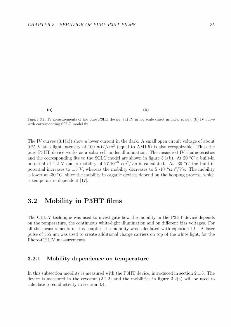
In this subsection mobility is measured with the P3HT device, introduced in section 2.1.5. Thedevice is measured in the cryostat (2.2.2) and the mobilities in figure 3.2(a) will be used tocalculate to conductivity in section 3.4.
CHAPTER 3. BEHAVIOR OF PURE P3HT FILMS 36
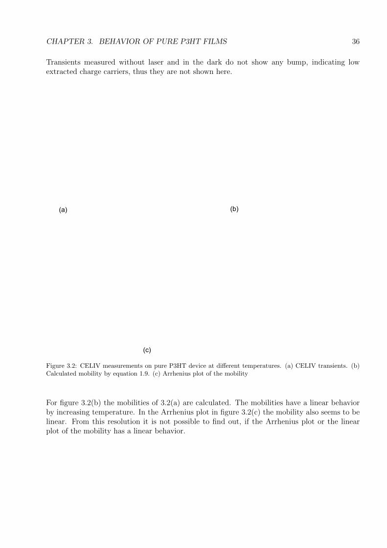
Transients measured without laser and in the dark do not show any bump, indicating lowextracted charge carriers, thus they are not shown here.
(a) (b)
(c)
Figure 3.2: CELIV measurements on pure P3HT device at different temperatures. (a) CELIV transients. (b)Calculated mobility by equation 1.9. (c) Arrhenius plot of the mobility
For figure 3.2(b) the mobilities of 3.2(a) are calculated. The mobilities have a linear behaviorby increasing temperature. In the Arrhenius plot in figure 3.2(c) the mobility also seems to belinear. From this resolution it is not possible to find out, if the Arrhenius plot or the linearplot of the mobility has a linear behavior.
CHAPTER 3. BEHAVIOR OF PURE P3HT FILMS 37
3.2.2 Mobility dependence on illumination intensity
In this subsection mobility measurements with the Schottky device, introduced in section 2.1.3,measured in the small chamber (2.2.1) are investigated.
(a) (b)
(c)
Figure 3.3: CELIV measurements on a P3HT device. (a) Mobility dependence on light at 20 C. (b) Mobilitydependence on light at -30 C. (c) Mobility overview at different temperatures and with/without laser
Classical CELIV curves are shown in figure 3.3(a). At -8 µs the laser is flashing. Positive andnegative charges are created over the whole film. Without a special device construction it isnot possible to distinguish between the extraction of holes and electrons. But if the deviceis thick enough, photo generated charges are not anymore in the bulk, but at the surface,which makes it possible to differ between holes and electrons. The bulk of the device has athickness of 230nm and thus the assumption of uniformly photo generated charges in the bulkis a good approximation. Therefore, we can not distinguish between hole and electron mobility,but it is generally accepted that the holes in pure P3HT film mainly contribute to the chargetransport [3]. An external DC bias is applied to minimize the electric field in the film prior tothe extraction pulse. At 0 µs the ramp starts. Due to the increasing voltage the depletion layer

CHAPTER 3. BEHAVIOR OF PURE P3HT FILMS 38
gets bigger and the holes are extracted by the ITO electrode. After equation 1.9, the time ofthe extraction peak gives the mobility.
The specific mobilities are shown calculated in the legend of figure 3.3(a) and 3.3(b) or in theoverview 3.3(c). One can recognize, the higher the illumination the higher the mobility. But, thelocal temperature of the film may increase upon illumination, and the higher the temperature,the higher the mobility. Even when we measure the surface temperature with a thermocouple,it is difficult to know, whether the mobility increase comes from higher illumination or highertemperature of the film. With a laser pulse the mobility gets lower compared to the transientswithout laser pulse.The charge carrier concentration (area below the bump) gets lower with higher light intensity.This is contrary to the expectations, since at least the same amount of charges should be photogenerated at higher light intensities. This phenomenon requires more investigation.
In figure 3.3(b) at -30 C the mobility dependence looks similar. Increasing the light intensityinduces higher mobility, although the mobility at 100 mW/cm2 (light intensity of one sun) isequal to the mobility in the dark. Without accurately knowing film temperature it is difficultto make any conclusion with high illuminated films. But we can see in this graph a agreementof the mobility with and without laser. The mobility at 1 sun with a laser pulse is 0.56 · 10−4
cm2/V s compared to 0.52 ·10−4 cm2/V s without laser pulse. And also the mobility in the darkwith 0.56 · 10−4cm2/V s is similar. At -30 C the mobility is not dependent on the laser pulseand at 20C the mobility is dependent on the laser pulse.
The current at 20 µs at 100 mW/cm2 and 20 C is 3.3 mA/cm2 and with a capacitor area ofA = 0.105 cm2 the real current is 0.33 mA. This current can be used in equation C = i dt
dU=
i/ramp = 0.33mA/(4.95V/20µs) = 1.33nF , which is the geometric capacitance of the diode.The thickness of the capacitor can be calculated by d = εε0A/C = 209 nm with ε = 3. This isin a good agreement with the thickness of the film measured by AFM (230 nm).
To summarize, the mobility in P3HT increases towards higher temperatures. Mobility dependson different permanent light intensities, probably due to the increasing temperature of the film.At 20 C the mobility gets lower with a laser pulse, whereas at -30 C the laser pulse does notaffect the mobility significantly.
3.2.3 Mobility dependence on bias voltage
In this subsection the mobility of the holes in the P3HT film, introduced in section 2.1.3,dependent on the applied bias and on the slope from the applied ramp will be measured anddiscussed. The device was measured in the small chamber (2.2.1).
CELIV transients with different bias voltages of 0 V and 0.95 V are shown in figure 3.4(a) and3.4(b). In picture 3.4(c) at a bias of 1.3 V, the diode is in forward bias, and we inject manycharge carriers into the film, which are visible in the negative current before the pulse begins.

CHAPTER 3. BEHAVIOR OF PURE P3HT FILMS 39
(a) (b)
(c)
Figure 3.4: Photo-CELIV measurements on a P3HT device at 20 C with different ramps and with: (a) Biasvoltage = 0 V, (b) Bias voltage = 0.95 V, (c) Bias voltage = 1.3 V
Mobilities Bias = 0V Bias = 0.95V Bias = 1.3VHigh slope 2.7 · 10−4cm2/V s 1.3 · 10−4cm2/V s 0.88 · 10−4cm2/V s
Middle slope 3.9 · 10−4cm2/V s 1.3 · 10−4cm2/V s 0.76 · 10−4cm2/V sLow slope 4.7 · 10−4cm2/V s 1.2 · 10−4cm2/V s 0.63 · 10−4cm2/V s
Table 3.1: Mobility dependence on bias voltage and on the slope of the voltage ramp
The mobility (table 3.1) seems to be dependent on the applied slope from the ramp and onthe bias voltage. The higher the bias, the lower the mobility. This may be because a higherbias voltage induces a smaller depletion layer (see in figure 3.9). And with a smaller depletionlayer one extracts more charges and it also takes more time (tmax) to extract them, becausethe mobile charges are distributed over a broader area in the film. The mobility calculations
CHAPTER 3. BEHAVIOR OF PURE P3HT FILMS 40
(equation 1.9) do not consider a depletion layer, one assumption is a uniform distribution ofmobile charges in the film.
At a bias of 0V the mobility decreases with a higher slope of the ramp (table 3.1). At a bias of1.3 V the mobility increases with a higher slope. But the mobility should not depend on theslope of the ramp, since we consider the ramp in equation 1.9. At a bias of 0.95 V the mobilityis almost independent on the slope of the voltage ramp. By measuring CELIV it is commonsense, to adjust the bias voltage to a value where the extracted charges before the ramp areminimized. This is how the bias voltage 0.95 V was defined in this CELIV measurements.
By using a bias voltage, which minimizes the extracted charges before the voltage ramp, themobility does not depend on the slope of the ramp.
3.3 Charge carrier concentration in P3HT films
3.3.1 Charge carrier concentration dependence on bias voltage
For this measurements the P3HT device (introduced here: 2.1.3) was used, which was measuredin the the small chamber (2.2.1).
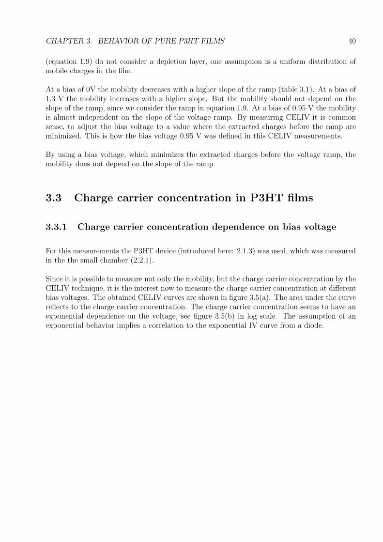
Since it is possible to measure not only the mobility, but the charge carrier concentration by theCELIV technique, it is the interest now to measure the charge carrier concentration at differentbias voltages. The obtained CELIV curves are shown in figure 3.5(a). The area under the curvereflects to the charge carrier concentration. The charge carrier concentration seems to have anexponential dependence on the voltage, see figure 3.5(b) in log scale. The assumption of anexponential behavior implies a correlation to the exponential IV curve from a diode.
CHAPTER 3. BEHAVIOR OF PURE P3HT FILMS 41
(a) (b)
Figure 3.5: Measuring charge carrier concentration by CELIV at 20 C, with a light intensity of 100 mW/cm2
and without a laser pulse. (a) CELIV Signal at different bias levels, where the area under the bump refers tothe charge carrier concentration. (b) Measured charge carrier concentration dependent on the bias voltage inlog scale.
The charge carrier concentration depends exponentially on the bias voltage. This gives riseto the assumption, that with CELIV one measures not only the intrinsic carriers but alsothe injected carriers. CELIV is not the appropriate technique to measure intrinsic chargecarrier concentration in low conductive materials, because with zero bias no visible charges areextracted and with a bias one probably extracts the injected charge carriers.
3.3.2 Charge carrier concentration dependence on temperature
3.3.2.1 Measured by impedance
In this subsection charge carrier concentration is measured with the P3HT device, introducedin section 2.1.5. The device is measured in the cryostat (2.2.2), and the charge carrier concen-trations will be used to calculate to conductivity in section 3.4.
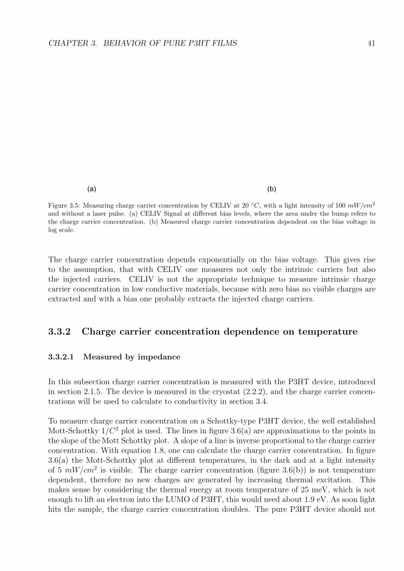
To measure charge carrier concentration on a Schottky-type P3HT device, the well establishedMott-Schottky 1/C2 plot is used. The lines in figure 3.6(a) are approximations to the points inthe slope of the Mott Schottky plot. A slope of a line is inverse proportional to the charge carrierconcentration. With equation 1.8, one can calculate the charge carrier concentration. In figure3.6(a) the Mott-Schottky plot at different temperatures, in the dark and at a light intensityof 5 mW/cm2 is visible. The charge carrier concentration (figure 3.6(b)) is not temperaturedependent, therefore no new charges are generated by increasing thermal excitation. Thismakes sense by considering the thermal energy at room temperature of 25 meV, which is notenough to lift an electron into the LUMO of P3HT, this would need about 1.9 eV. As soon lighthits the sample, the charge carrier concentration doubles. The pure P3HT device should not
CHAPTER 3. BEHAVIOR OF PURE P3HT FILMS 42
act like a photo diode, and charges should not be generated by light, since there is no acceptorin the bulk to separate the excitons. But charges can also be photo generated at impuritiesor at the junctions to the electrodes (see section 3.3.3), this likely causes the increase of thecharge carrier concentration under illumination.
(a)
(b)
Figure 3.6: Mott-Schottky plot of P3HT device at different temperatures and light intensities (a). Impedanceis measured at 110 Hz. From (a) charge carrier concentration is calculated and shown in (b) at differenttemperatures
The charge carrier concentration in a P3HT device does not depend on the temperature, anddoubles with an irradiance of 5 mW/cm2.
3.3.2.2 Measured by CELIV
In this subsection the carrier concentration is measured with the CELIV technique. The deviceis introduced in section 2.1.3, and was measured in the small chamber (2.2.1). The charge
CHAPTER 3. BEHAVIOR OF PURE P3HT FILMS 43
carrier concentrations will be used to calculate to conductivity in section 3.4.
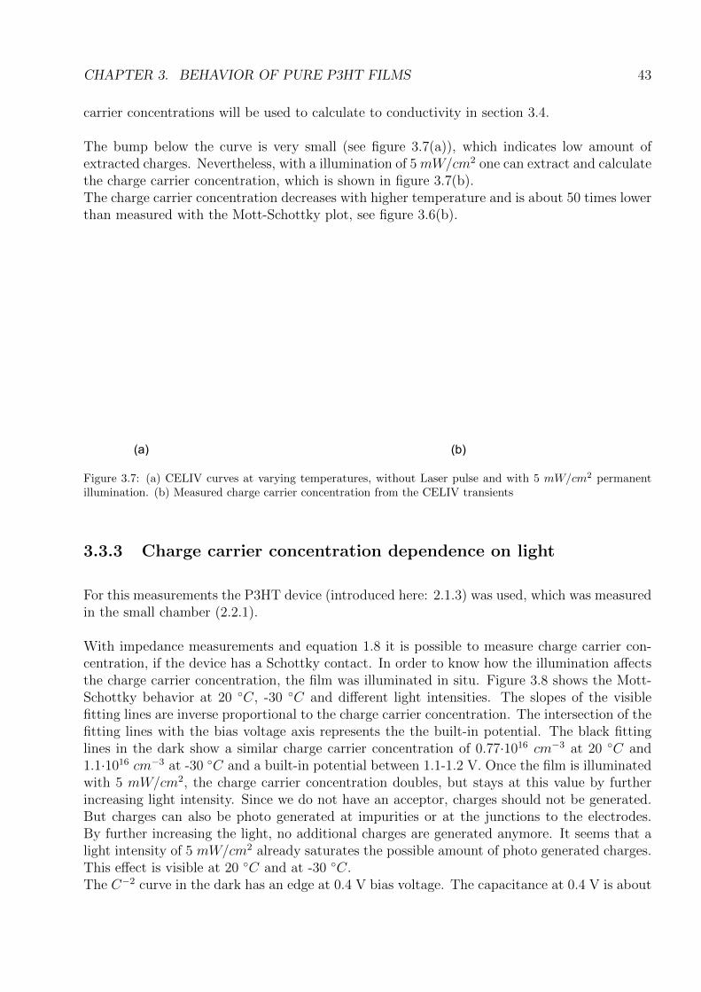
The bump below the curve is very small (see figure 3.7(a)), which indicates low amount ofextracted charges. Nevertheless, with a illumination of 5 mW/cm2 one can extract and calculatethe charge carrier concentration, which is shown in figure 3.7(b).The charge carrier concentration decreases with higher temperature and is about 50 times lowerthan measured with the Mott-Schottky plot, see figure 3.6(b).
(a) (b)
Figure 3.7: (a) CELIV curves at varying temperatures, without Laser pulse and with 5 mW/cm2 permanentillumination. (b) Measured charge carrier concentration from the CELIV transients
3.3.3 Charge carrier concentration dependence on light
For this measurements the P3HT device (introduced here: 2.1.3) was used, which was measuredin the small chamber (2.2.1).
With impedance measurements and equation 1.8 it is possible to measure charge carrier con-centration, if the device has a Schottky contact. In order to know how the illumination affectsthe charge carrier concentration, the film was illuminated in situ. Figure 3.8 shows the Mott-Schottky behavior at 20 C, -30 C and different light intensities. The slopes of the visiblefitting lines are inverse proportional to the charge carrier concentration. The intersection of thefitting lines with the bias voltage axis represents the the built-in potential. The black fittinglines in the dark show a similar charge carrier concentration of 0.77·1016 cm−3 at 20 C and1.1·1016 cm−3 at -30 C and a built-in potential between 1.1-1.2 V. Once the film is illuminatedwith 5 mW/cm2, the charge carrier concentration doubles, but stays at this value by furtherincreasing light intensity. Since we do not have an acceptor, charges should not be generated.But charges can also be photo generated at impurities or at the junctions to the electrodes.By further increasing the light, no additional charges are generated anymore. It seems that alight intensity of 5 mW/cm2 already saturates the possible amount of photo generated charges.This effect is visible at 20 C and at -30 C.The C−2 curve in the dark has an edge at 0.4 V bias voltage. The capacitance at 0.4 V is about
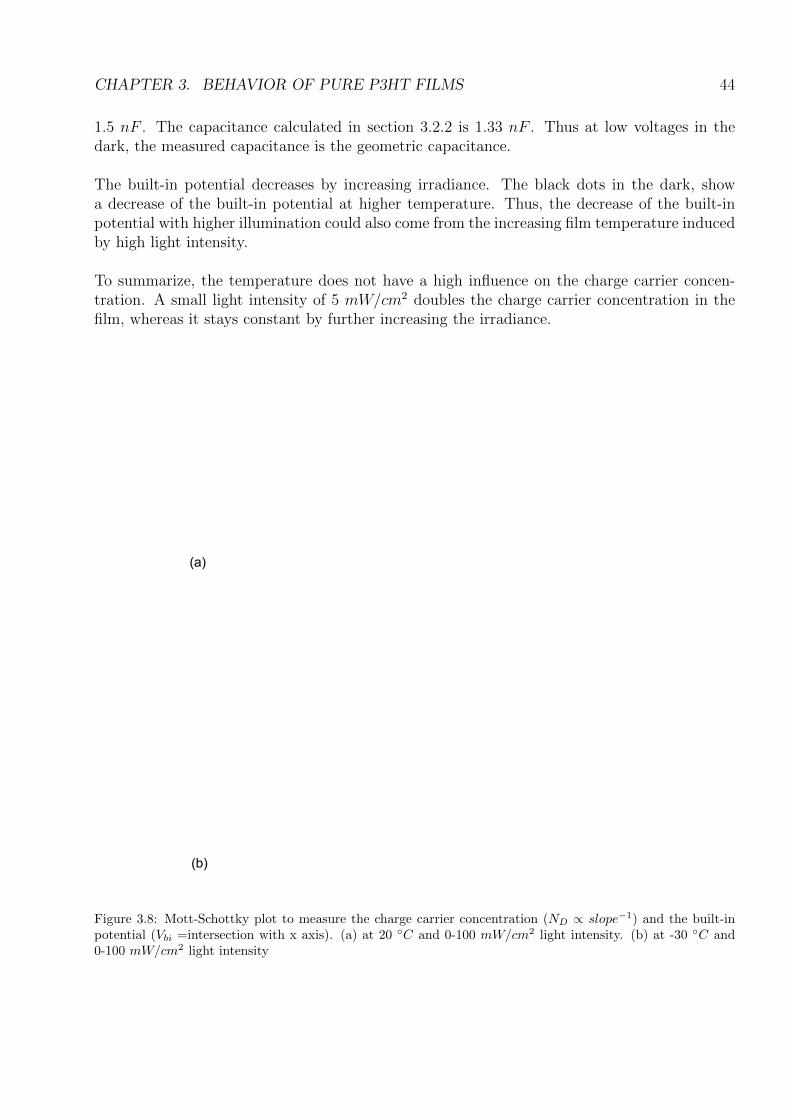
CHAPTER 3. BEHAVIOR OF PURE P3HT FILMS 44
1.5 nF . The capacitance calculated in section 3.2.2 is 1.33 nF . Thus at low voltages in thedark, the measured capacitance is the geometric capacitance.
The built-in potential decreases by increasing irradiance. The black dots in the dark, showa decrease of the built-in potential at higher temperature. Thus, the decrease of the built-inpotential with higher illumination could also come from the increasing film temperature inducedby high light intensity.
To summarize, the temperature does not have a high influence on the charge carrier concen-tration. A small light intensity of 5 mW/cm2 doubles the charge carrier concentration in thefilm, whereas it stays constant by further increasing the irradiance.
(a)
(b)
Figure 3.8: Mott-Schottky plot to measure the charge carrier concentration (ND ∝ slope−1) and the built-inpotential (Vbi =intersection with x axis). (a) at 20 C and 0-100 mW/cm2 light intensity. (b) at -30 C and0-100 mW/cm2 light intensity

CHAPTER 3. BEHAVIOR OF PURE P3HT FILMS 45
3.3.4 Depletion layer thickness dependencies
With the built-in potential and the charge carrier concentration from last section (3.3.3) onecan calculate the depletion layer thickness by using equation 1.5, which is dependent on thebias voltage. This equation is only valid, if the curve in the Mott-Schottky plot is linear. Theresults and the marked valid regions from this calculations are shown in figure 3.9 at differenttemperatures and illuminations.
valid region
Figure 3.9: Depletion layer thickness of a P3HT device over bias voltage at different temperatures and lightintensities. The valid region shows where the Mott-Schottky plot is linear
Measured by AFM the thickness of the film is 230 nm. The depletion layer in a Schottkydiode changes its thickness due to different bias voltages, and therefore the capacitance getslower, the bigger the depletion layer is. Once the depletion layer is thicker than the device, oneshould not observe any change in the capacitance. In the dark at negative bias in figure 3.9the depletion layer gets bigger than the thickness of the device, and the capacitance should notchange anymore. This, we can observe in figure 3.8. The still visible error may come from anerror of the measured active area. Also, the dielectric constant could be different from 3. Wealready got a smaller thickness of the film in CELIV measurement (209 nm), where we alsouses the same dielectric constant. Under light the thickness of the depletion layer is not biggerthan the real thickness of 230 nm, in the measured voltage range.
Measured by two completely different methods, AFM and Mott-Schottky plot, the thicknessof the film is very similar. The well established theory of Mott-Schottky to define the chargecarrier concentration and the depletion layer thickness seems to be accurate in a pure P3HTfilm.
3.3.5 Impedance spectroscopy
Impedance spectroscopy is a tool to find the equivalent circuit for a device. An equivalentcircuit model gives information about the resistance behavior.
CHAPTER 3. BEHAVIOR OF PURE P3HT FILMS 46
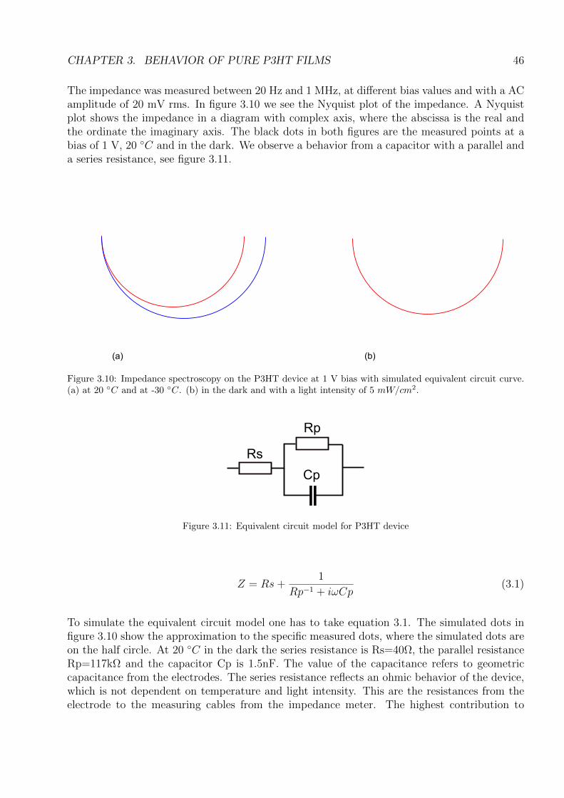
The impedance was measured between 20 Hz and 1 MHz, at different bias values and with a ACamplitude of 20 mV rms. In figure 3.10 we see the Nyquist plot of the impedance. A Nyquistplot shows the impedance in a diagram with complex axis, where the abscissa is the real andthe ordinate the imaginary axis. The black dots in both figures are the measured points at abias of 1 V, 20 C and in the dark. We observe a behavior from a capacitor with a parallel anda series resistance, see figure 3.11.
(a) (b)
Figure 3.10: Impedance spectroscopy on the P3HT device at 1 V bias with simulated equivalent circuit curve.(a) at 20 C and at -30 C. (b) in the dark and with a light intensity of 5 mW/cm2.
Rp
Rs
Cp
Figure 3.11: Equivalent circuit model for P3HT device
Z = Rs+1
Rp−1 + iωCp(3.1)
To simulate the equivalent circuit model one has to take equation 3.1. The simulated dots infigure 3.10 show the approximation to the specific measured dots, where the simulated dots areon the half circle. At 20 C in the dark the series resistance is Rs=40Ω, the parallel resistanceRp=117kΩ and the capacitor Cp is 1.5nF. The value of the capacitance refers to geometriccapacitance from the electrodes. The series resistance reflects an ohmic behavior of the device,which is not dependent on temperature and light intensity. This are the resistances from theelectrode to the measuring cables from the impedance meter. The highest contribution to

CHAPTER 3. BEHAVIOR OF PURE P3HT FILMS 47
the series resistance in the device is the ITO electrode. The parallel resistance is the ohmiccontribution from the film. It depends on the bias voltage, temperature and light intensity.In figure 3.10(a) the parallel resistance gets higher at lower temperatures. The same occursby irradiating the device, but the effect is much higher with light. The parallel resistance Rpdecreases from 117kΩ to 11kΩ with 5 mW/cm2.
At a forward bias voltage of 1V, small illumination of 5 mW/cm2 decreases the resistance ofthe film about a factor of 10. The resistance of the film also decreases with higher temperature.
3.4 Conductivity of P3HT films
In this section conductivity is measured and calculated with the P3HT device, introduced insection 2.1.5 and measured in the cryostat (2.2.2).
3.4.1 IV behavior in P3HT device
Following IV curves show the function of a device. In figure 3.12(a) the IV curve from thefurther used P3HT Schottky device and in (b) the modified 4 wire measurement resistance isshown. The linear IV behavior in figure (b) is a requirement for the 4 wire measurement, sinceit reflects a constant resistance over the whole voltage range.
(a) (b)
20°C, dark
Figure 3.12: IV curves of P3HT device. (a) Schottky diode. (b) IV curve from modified 4 wire measurement
CHAPTER 3. BEHAVIOR OF PURE P3HT FILMS 48
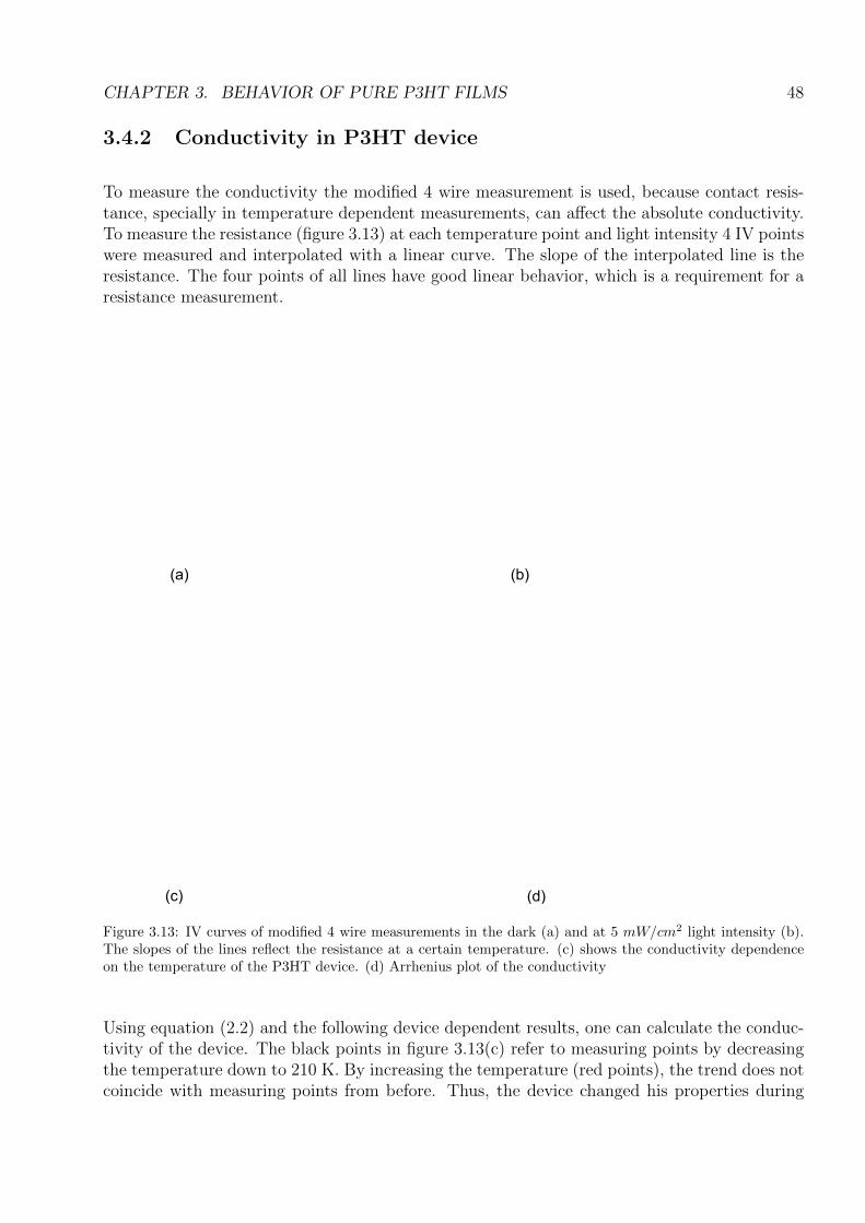
3.4.2 Conductivity in P3HT device
To measure the conductivity the modified 4 wire measurement is used, because contact resis-tance, specially in temperature dependent measurements, can affect the absolute conductivity.To measure the resistance (figure 3.13) at each temperature point and light intensity 4 IV pointswere measured and interpolated with a linear curve. The slope of the interpolated line is theresistance. The four points of all lines have good linear behavior, which is a requirement for aresistance measurement.
(a) (b)
(c) (d)
Figure 3.13: IV curves of modified 4 wire measurements in the dark (a) and at 5 mW/cm2 light intensity (b).The slopes of the lines reflect the resistance at a certain temperature. (c) shows the conductivity dependenceon the temperature of the P3HT device. (d) Arrhenius plot of the conductivity
Using equation (2.2) and the following device dependent results, one can calculate the conduc-tivity of the device. The black points in figure 3.13(c) refer to measuring points by decreasingthe temperature down to 210 K. By increasing the temperature (red points), the trend does notcoincide with measuring points from before. Thus, the device changed his properties during
CHAPTER 3. BEHAVIOR OF PURE P3HT FILMS 49
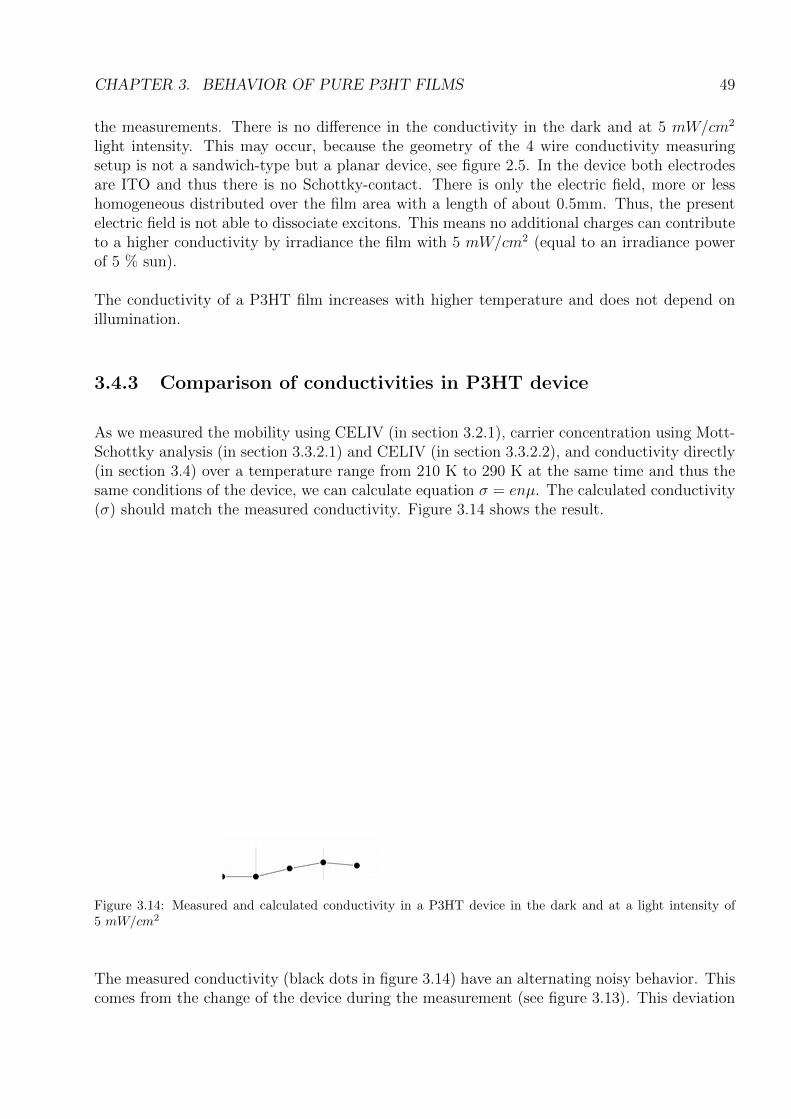
the measurements. There is no difference in the conductivity in the dark and at 5 mW/cm2
light intensity. This may occur, because the geometry of the 4 wire conductivity measuringsetup is not a sandwich-type but a planar device, see figure 2.5. In the device both electrodesare ITO and thus there is no Schottky-contact. There is only the electric field, more or lesshomogeneous distributed over the film area with a length of about 0.5mm. Thus, the presentelectric field is not able to dissociate excitons. This means no additional charges can contributeto a higher conductivity by irradiance the film with 5 mW/cm2 (equal to an irradiance powerof 5 % sun).
The conductivity of a P3HT film increases with higher temperature and does not depend onillumination.
3.4.3 Comparison of conductivities in P3HT device
As we measured the mobility using CELIV (in section 3.2.1), carrier concentration using Mott-Schottky analysis (in section 3.3.2.1) and CELIV (in section 3.3.2.2), and conductivity directly(in section 3.4) over a temperature range from 210 K to 290 K at the same time and thus thesame conditions of the device, we can calculate equation σ = enµ. The calculated conductivity(σ) should match the measured conductivity. Figure 3.14 shows the result.
Figure 3.14: Measured and calculated conductivity in a P3HT device in the dark and at a light intensity of5 mW/cm2
The measured conductivity (black dots in figure 3.14) have an alternating noisy behavior. Thiscomes from the change of the device during the measurement (see figure 3.13). This deviation

CHAPTER 3. BEHAVIOR OF PURE P3HT FILMS 50
is not visible in the calculated curves. The calculated curves are based on the Schottky diode.The Schottky diode did not change during the measurement, possibly due to shielding of thesemiconductor to the atmospheric conditions by the metal electrode.At 210 K the measured conductivity is 2 to 3 times higher than the calculated conductivity. Thecalculated curve at 5 mW/cm2 is higher compared to the curve in the dark, because the chargecarrier density doubles with 5 mW/cm2 light intensity. At 290 K the error factor betweencalculated and measured conductivity is 2 to 5. The calculated curve with the mobility andthe charge carrier concentration measured by CELIV (blue squares in figure 3.14) is about 100times lower than the measured conductivity. This comes mostly from the 50 times lower chargecarrier concentration measured with the CELIV technique.This difference in the conductivities can have several sources. First, the geometry of the deviceto measure 4 wire resistance and the geometry of the Schottky diode are very different. In theSchottky diode the charges move perpendicular to the substrate, whereas the charges in the 4wire setup move parallel to the substrate. The polymers in the P3HT can have preferences toorientate themselves with respect to the substrate. Usually the backbones of the polymer tendto crystallize parallel to the substrate. Thus, the conductivity in 4 wire measurement would behigher, which is the case. Due to the different geometry also the electric field is different. Theelectric field in the Schottky diode is about 3 orders of magnitude higher, because of the muchlower distance between the electrodes. But after Poole-Frenkel-type law the mobility increaseswith higher electric field, thus the conductivity in the Schottky diode should be higher, but itis lower.Another possible error could be the mobility determination by CELIV. The mobilities in CELIVwere higher if the laser was not in use. But, due to the low charge carrier concentration in P3HTthe visible peak in CELIV was difficult to define. This would mean that the photo generatedcharges do not have the same mobility as the intrinsic charges. Further, as soon charges arephoto-generated in the film, the diffusion current may contribute to the drift current. Butthe used equation for the mobility (1.9) is only based on the drift current, this could be anadditional error.
Measuring the conductivities at different temperatures give 2 to 5 times higher conductivitiesthan calculating the conductivities by determining the mobility with CELIV and the chargecarrier concentration by the Mott-Schottky plot. Because the mobility is higher at highertemperatures, the conductivity also increases with higher temperature. The low charge carrierconcentration from CELIV gives a 2 orders of magnitude lower conductivity.
3.5 P3HT film measurement summary
The mobilities, measured by CELIV and SCLC are listed in table 3.2. The mobility of thecharge carriers in a P3HT film is higher with higher temperature. This can be seen between20 C and -30 C. But also with a light intensity of 100 mW/cm2 the film gets warm, andshows a higher mobility. Mobility measured by SCLC and CELIV gives similar results and thesame trends, regarding temperature dependence. The measured mobility in the device for thecryostat is higher than in the device for the small chamber. The production procedure is the

CHAPTER 3. BEHAVIOR OF PURE P3HT FILMS 51
same, except the final annealing step in the device from the small chamber was accidentally notmade. Annealing causes a higher cristallinity of the P3HT, which leads to a higher mobility.This may explain the 3 times higher mobility.The charge carrier concentration in a P3HT device, see table 3.3, more than doubles with asmall light intensity of 5 mW/cm2, but by further increasing the light it stays more or less atthe same value. The charge carrier concentration is not dependent on the temperature. Thecharge carrier concentrations from the different devices are similar. Thus, the annealing stepdoes not affect the charge carrier concentration.
MobilitiesP3HT darksmall chamber
P3HT 100mW/cm2
small chamberP3HT darkcryostat
CELIV 20 C [10−4cm2/V s] 1.3 1.7 3CELIV -30 C [10−4cm2/V s] 0.56 0.56 1.8SCLC 20 C [10−4cm2/V s] 2.7 - -SCLC -30 C [10−4cm2/V s] 0.5 - -
Table 3.2: Measured mobilities with small chamber and cryostat, dependent on light and temperature
Charge carrierconcentration
P3HTdarksmallchamber
P3HT5mW/cm2smallchamber
P3HT100mW/cm2small cham-ber
P3HTdarkcryostat
P3HT5mW/cm2cryostat
20 C [1016cm−3] 0.7 1.9 1.7 0.8 1.6-30 C [1016cm−3] 0.97 1.9 2 0.8 1.6
Table 3.3: Measured charge carrier concentration with small chamber and cryostat, dependent on light andtemperature
Overall the mobility, measured with different techniques, and charge carrier concentration showgood and reproducible values and trends, regarding temperatures and illumination behavior.Where the used techniques, except the charge carrier concentration measurements by CELIV,show a good consistency with the conductivity measurements.

Chapter 4
Behavior of P3HT:PCBMbulk-heterojunction films
4.1 IV behavior in P3HT:PCBM films
In this section IV measurements with the BHJ device, introduced in section 2.1.4, measuredin the the small chamber (2.2.1) are shown. The IV curves (figure 4.1) show temperature andlight dependent behavior. The higher the light intensity, the higher the current in reverse bias,since more photo-generated charge carriers are available to participate in the current. At lowertemperatures the dark current and the current in forward bias is lower.
(a) (b)
Figure 4.1: IV curves of a BHJ solar cell. (a) different light intensities. (b) different temperatures
In figure 4.2 the mobility is calculated with the Mott-Gurney relation (1.1). At -30 C and at20 C the mobility is slightly lower with an illuminated film compared to the dark.With higher temperature the mobility gets higher. This is visible in the dark and with a white
52

CHAPTER 4. BEHAVIOR OF P3HT:PCBM BULK-HETEROJUNCTION FILMS 53
(a) (b)
Figure 4.2: IV curve in space charge limited current regime and specific calculated mobility. (a) in the dark.(b) with 100 mW/cm2 light intensity
light intensity of 100 mW/cm2.
4.2 Mobility in P3HT:PCBM films
4.2.1 Mobility dependence on temperature
In this section mobility is measured and calculated with a P3HT-PCBM device (introduced insection 2.1.6). The device is measured in the cryostat (2.2.2), and the mobility will be used tocalculate to conductivity in section 4.4.3.
The mobility of the charge carriers is measured by CELIV. In figure 4.3(a) the current transientsin the dark are shown. The higher the temperature, the more mobile charge carriers are availableand thus the peak is better recognizable. At 220 K the peak is very low and in this plot, it isdifficult to define the time from the peak (tmax), but with a higher zoom the peak can be defined.In figure 4.3(b), the illuminated film keeps the charge carrier concentration on a certain leveland therefore the peaks are good recognizable, also at low temperatures. The CELIV transientin a P3HT-PCBM device represents the sum of the extracted electrons and the extracted holes.Thus, the measured peak tmax gives the mobility somehow averaged between the mobilities ofthe two materials.

CHAPTER 4. BEHAVIOR OF P3HT:PCBM BULK-HETEROJUNCTION FILMS 54
(a) (b)
(c) (d)
Figure 4.3: CELIV measurements on organic solar cell in the dark (a) and with irradiance of 5 mW/cm2 (b).Calculated mobility at different temperatures in linear scale(c) and in the Arrhenius plot(d).
In figure 4.3(c) and 4.3(d) the mobility is calculated by equation 1.9. In 4.3(c) the mobility in thedark and at 5 mW/cm2 is shown temperature dependent. The mobility at room temperaturehas about the same value. At 220 K the mobility is 3 times higher with an illumination of5 mW/cm2 compared to the mobility in the dark. This may come from the dependence of themobility on the charge carrier concentration. The higher charge carrier concentration (the bumpunder the curve) induces a higher mobility. At room temperature this difference is not visibleanymore, this means, the contribution of the thermal generated charges at room temperatureis higher than the photo-generated charges at an irradiance of 5 mW/cm2.The noise or zig-zag behavior of the dark mobility curve comes from a change of the deviceduring the measurements. The temperature measurements were done in the order: 300 K, 280K, 260 K, 240 K, 230 K, 220 K, 225 K, 235 K, 250 K, 270 K, 290 K.
The higher the temperature the higher the mobility. Irradiance increased the mobility if thetemperature is below 290 K.

CHAPTER 4. BEHAVIOR OF P3HT:PCBM BULK-HETEROJUNCTION FILMS 55
4.2.2 Mobility dependence on illumination intensity
For the CELIV mobility measurements, the BHJ device (introduced in section 2.1.4) was used,which was measured in the the small chamber (2.2.1). As already mentioned, in the CELIVtransient the measured tmax represents an averaged mobility of the holes and electrons of P3HTand PCBM.Measuring the P3HT device, gives higher mobilities at higher temperatures. The mobilitiesin the solar cell (figure 4.4) have a similar temperature behavior. Higher temperature induceshigher mobilities. Except in the dark, the mobility stays at 1.2 · 10−4cm2/V s at -30 C and20 C. The mobility also decreases with higher irradiance, this can not be a temperature effectlike in the P3HT device, because with higher irradiance the temperature should be higher andthus the mobility higher. Therefore illumination does affect the mobility of the charge carriersin the device.
It has been theorized that increasing the charge carrier concentration will fill the low lyingstates, allowing for easier hopping dynamics [17]. The mobility is expected to increase withhigher carrier concentration. Figure 4.4 shows the measured data have an opposite trend, whichmay be due to the limits of the validity of equation 1.9 when ∆j is larger than j(0).
(a) (b)
Figure 4.4: CELIV transients to measure mobility at different light intensities. (a) at 20 C and (b) at -30 C
4.2.3 RC time constant in CELIV measurement
In CELIV measurement a voltage ramp is applied on a device and the current response ismeasured time dependent. In this section we calculate the influence of the RC contributionduring the measurement. RC means a series connection of resistor and capacitor. By applyinga ramp voltage on a RC circuit, the current response needs some time to keep up with thederivative of the voltage ramp. The time until the current could respond to the voltage rampcan be calculated. τ = RC, where τ is the so called time constant in unit seconds, R theresistor and C the capacitor. After the time of τ the current has reached 63.2 % of his finalvalue, and after 5τ the current has reached 99.3 % of his final value. Usually in electronic
CHAPTER 4. BEHAVIOR OF P3HT:PCBM BULK-HETEROJUNCTION FILMS 56
circuits one says, is the system slower than 5τ , then there is no time dependent contributionfrom the RC circuit. The time 5τ for the used CELIV setup by measuring an organic solar cellwill be calculated in this section.
In according to the film thickness of 160 nm the geometric capacitance is 1.83 nF. Rs containsthe series resistance of the device and the internal resistance of the oscilloscope, which is50 Ω. The series resistance of the device can be measured at high frequencies with impedancespectroscopy and is 27 Ω (not shown in this thesis). Based on this results we get:
5 τ = 5RC = 5 · (27 + 50)Ω · 1.83nF = 0.7µs
The time for the current response from zero to the maximum in an equivalent capacitor takesabout 0.7 µs. The CELIV transient is 20 µs long and the peak (tmax) usually between 2 µsand 5 µs. Thus RC does not affect significantly the tmax value, which is used to calculate themobility.
4.3 Charge carrier concentration in P3HT:PCBM films
4.3.1 Charge carrier concentration dependence on temperature
In this subsection the P3HT-PCBM device introduced in section 2.1.6 is used. The device ismeasured in the cryostat (2.2.2), and the charge carrier concentrations will be used to calculateto conductivity in section 4.4.3.
The Mott Schottky plot, in figure 4.5(a), shows the capacitance behavior of a solar cell. Thehigher the bias, the higher the capacitance, since the depletion layer gets smaller. The linesare approximations to the points in the slope of the Mott Schottky plot. A slope of a line isinversely proportional to the charge carrier concentration. With equation 1.8, one can calculatethe charge carrier concentration.Figure 4.5(b) shows the calculated charge carrier concentration at different temperatures inthe dark and with an irradiance of 5 mW/cm2. In the dark and under illumination the chargecarrier concentration gets lower with higher temperatures. Although in CELIV an oppositedependence of the charge carrier concentration on the temperature was recognized, see chapter4.2.1, where the area under the bump gets higher with higher temperatures. The charge carrierconcentration at 5 mW/cm2 irradiance is about 10 times higher than in the dark in the wholemeasured temperature range.

CHAPTER 4. BEHAVIOR OF P3HT:PCBM BULK-HETEROJUNCTION FILMS 57
(a)
(b)
Figure 4.5: Mott Schottky plot of a P3HT-PCBM solar cell (a) in the dark and at 5 mW/cm2. The calculatedcharge carrier concentrations (b) at different temperatures and light intensities.
Comparing the charge carrier concentrations of the solar cell with the P3HT device, one cansee at 5 mW/cm2 light intensity the P3HT device (figure 3.6) has a lower charge carrier concen-tration compared to the solar cell, but in the dark the charge carrier concentration is higher inthe P3HT device than in the solar cell. With illumination the charge carriers can be separatedat the junction and thus the solar cell has a higher charge carrier concentration. In the darkit is not clear, why the charge carrier concentration is smaller in solar cell than in the P3HTdevice. One can assume, that in the dark the charges in a P3HT-PCBM device mainly arepresent in the P3HT. It is understandable that the charge carrier concentration in the darkwould be lower by roughly a factor of 2, because a significant volume fraction of the bulk isoccupied by PCBM.
The charge carrier concentration gets smaller with higher temperatures. 5 mW/cm2 irradiancegenerates 10 times more charges than in the dark, and this factor is not temperature dependent.
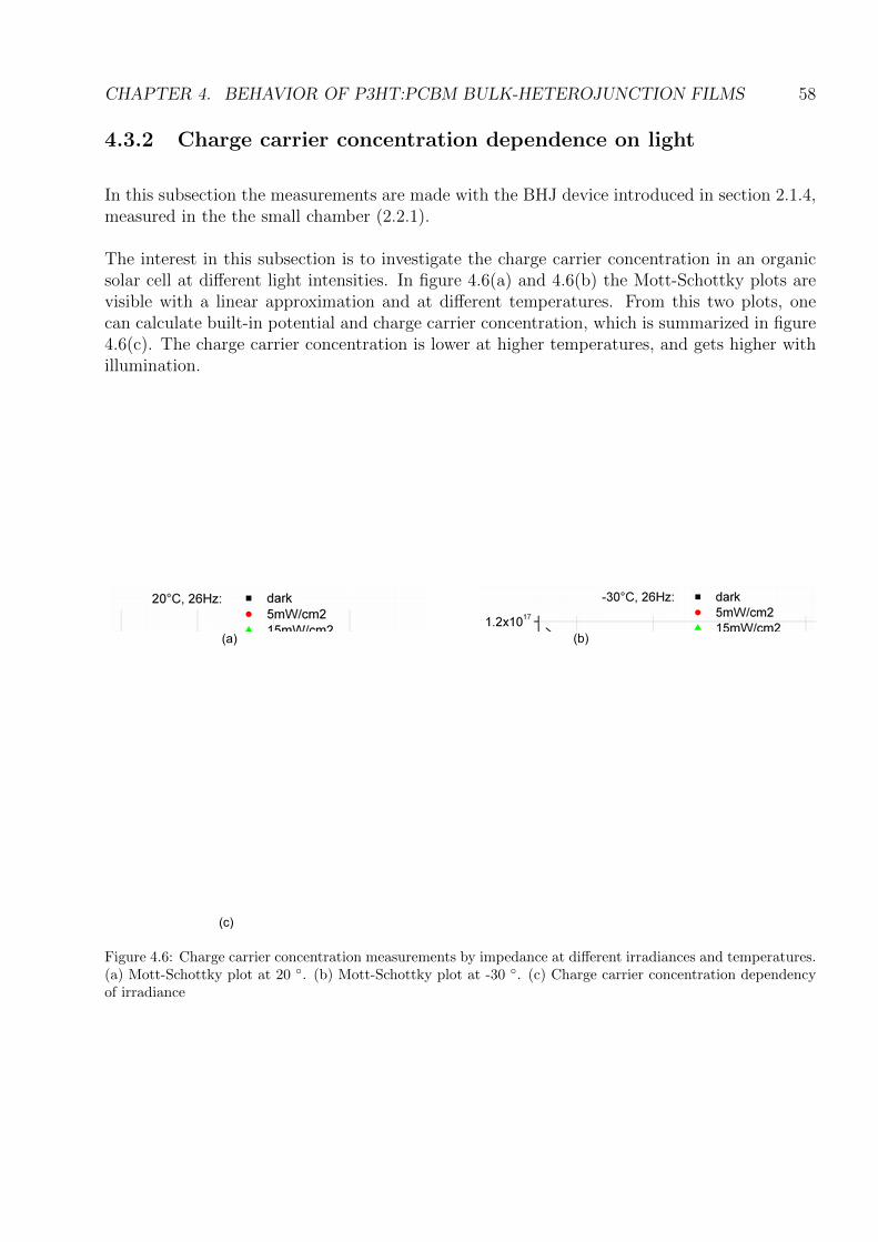
CHAPTER 4. BEHAVIOR OF P3HT:PCBM BULK-HETEROJUNCTION FILMS 58
4.3.2 Charge carrier concentration dependence on light
In this subsection the measurements are made with the BHJ device introduced in section 2.1.4,measured in the the small chamber (2.2.1).
The interest in this subsection is to investigate the charge carrier concentration in an organicsolar cell at different light intensities. In figure 4.6(a) and 4.6(b) the Mott-Schottky plots arevisible with a linear approximation and at different temperatures. From this two plots, onecan calculate built-in potential and charge carrier concentration, which is summarized in figure4.6(c). The charge carrier concentration is lower at higher temperatures, and gets higher withillumination.
(a) (b)
(c)
Figure 4.6: Charge carrier concentration measurements by impedance at different irradiances and temperatures.(a) Mott-Schottky plot at 20 . (b) Mott-Schottky plot at -30 . (c) Charge carrier concentration dependencyof irradiance

CHAPTER 4. BEHAVIOR OF P3HT:PCBM BULK-HETEROJUNCTION FILMS 59
4.3.3 Depletion layer thickness dependencies
Figure 4.7: Depletion layer thickness over bias voltage in a P3HT-PCBM organic solar cell at different temper-atures and irradiance.
After equation 1.5 the depletion layer thickness depends on the built-in potential and the chargecarrier concentration. The depletion layer thickness is shown in figure 4.7. At a voltage of 0.3V, which reflects the maximum power point of the IV curve, the thickness of the depletionlayer under illumination is zero. At -1.6 V in all conditions the depletion layer does not expandover geometric film thickness of 160 nm, yet. The higher the irradiance, the higher the chargecarrier concentration and thus the smaller the depletion layer. Also, due to higher charge carrierconcentrations at lower temperatures the depletion layer gets smaller.
At 0.3 V the thickness of the depletion layer in the film under illumination is almost zero. Thus,in a solar cell the bulk is not affected by the high electric field from the depletion layer. Thissupports the idea, that the charge transport in an organic solar cell may not be affected by theelectric field of the depletion layer and thus could be diffusion dominated, which is still underdiscussion.
4.4 Conductivity of P3HT:PCBM films
In this section conductivity is measured and calculated with a P3HT-PCBM device (introducedin section 2.1.6), which is measured in the cryostat (2.2.2).
CHAPTER 4. BEHAVIOR OF P3HT:PCBM BULK-HETEROJUNCTION FILMS 60
4.4.1 IV behavior in P3HT:PCBM device
The IV curve is shown first, to give information about working range of the device. Underillumination of one sun, the solar cell has a short circuit current of 4.4 mA/cm2, and opencircuit voltage of 0.58 V .
(a) (b)
Figure 4.8: IV curves of P3HT-PCBM solar cell. (a) Linear scale. (b) Logarithmic scale
4.4.2 Conductivity in P3HT:PCBM device
The conductivity in the P3HT-PCBM device is measured with the modified 4 wire technique(see figure 2.5 and device geometry 2.1.6). This has been done at different temperatures, inthe dark and with an irradiance of 5 mW/cm2. In figure 4.9(a) the voltage-current diagram isshown. Since the resistance should have a ohmic behavior, the measured points can be con-nected with a linear line. The slope of the line gives the resistance at the specific temperature.In figure 4.9(b) the same is shown, but with illumination. The voltage is still positive at zerocurrent. This means, in the second quadrant the device works as a solar cell. This is surprising,because the device is symmetric regarding used contact metals (see figure 2.5). There must besome unsymmetrical geometry which forces the separated charges to be collected rather at oneelectrode than at the other. The measured voltage still has a linear dependence on the current,thus the slope still gives the resistance.
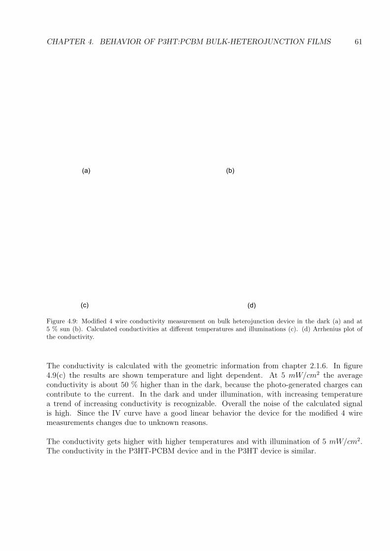
CHAPTER 4. BEHAVIOR OF P3HT:PCBM BULK-HETEROJUNCTION FILMS 61
(a) (b)
(c) (d)
Figure 4.9: Modified 4 wire conductivity measurement on bulk heterojunction device in the dark (a) and at5 % sun (b). Calculated conductivities at different temperatures and illuminations (c). (d) Arrhenius plot ofthe conductivity.
The conductivity is calculated with the geometric information from chapter 2.1.6. In figure4.9(c) the results are shown temperature and light dependent. At 5 mW/cm2 the averageconductivity is about 50 % higher than in the dark, because the photo-generated charges cancontribute to the current. In the dark and under illumination, with increasing temperaturea trend of increasing conductivity is recognizable. Overall the noise of the calculated signalis high. Since the IV curve have a good linear behavior the device for the modified 4 wiremeasurements changes due to unknown reasons.
The conductivity gets higher with higher temperatures and with illumination of 5 mW/cm2.The conductivity in the P3HT-PCBM device and in the P3HT device is similar.

CHAPTER 4. BEHAVIOR OF P3HT:PCBM BULK-HETEROJUNCTION FILMS 62
4.4.3 Comparison of conductivities in P3HT:PCBM device
As we measured the mobility using CELIV (in section 4.2.1), carrier concentration using Mott-Schottky analysis (in section 4.3.1), and conductivity directly (in section 4.4.2) over a tem-perature range from 215 K to 300 K at the same time and thus the same conditions of thedevice, we can calculate equation σ = enµ. The calculated conductivity (σ) should match themeasured conductivity. Figure 4.10 shows the result.
Figure 4.10: Measured and calculated conductivities from P3HT-PCBM heterojunction device at differenttemperatures, in the dark and under a light intensity of 5 mW/cm2.
The circle and the squares in figure 4.10 represent the measured conductivity, which is similarto the measured conductivity in pure P3HT (see 3.14). But here in the P3HT-PCBM devicea clear difference between the measured conductivity in the dark and under illumination isrecognizable. The measured conductivity under illumination is about 2 times higher. Thiscould come from a higher charge carrier concentration, shown in figure 4.5. The calculatedcurve at 5 mW/cm2 at 220 K is about 3 times smaller and at 300 K about 7 times smallerthan the measured conductivity. The mismatch gets bigger in the dark, where the calculatedconductivity is 50-80 times lower than the measured conductivity.At 290 K the conductivities of the P3HT device and the BHJ device is similar. But the chargecarrier concentration and the mobility in the P3HT-PCBM device is about 3 times lower at290 K than in the P3HT device. Thus the lower charge carrier concentrations and the lowermobilities contribute to the mismatch between the measured and calculated conductivities. Thereason of the mismatch requires more investigation.

CHAPTER 4. BEHAVIOR OF P3HT:PCBM BULK-HETEROJUNCTION FILMS 63
In the conductivity measurements holes may dominate the charge transport, since the 2 ITOelectrodes make a quasi ohmic contact to the HOMO of the P3HT. Whereas the PCBM as aelectron conductor has a higher LUMO level than the ITO work function, and thus can notcontribute to the charge transport in the dark.
The mismatch between calculated and measured conductivities is higher than in the P3HTdevice. In the dark the lower charge carrier concentration and the lower mobility is responsiblefor the 50-80 times lower conductivity. With a light intensity of 5 mW/cm2 the calculatedconductivity is 3 to 7 times too low.
4.5 P3HT:PCBM film measurement summary
The mobilities, measured by CELIV and SCLC are listed in table 4.1. In all conditions, highertemperature induces an equal or higher mobility. Mobility measured by SCLC shows similartrends like the mobility measured by CELIV. But the changes in the mobility due to differentlight intensities are higher in the CELIV mobility.
Mobilities
BHJdarksmallchamber
BHJ100mW/cm2
smallchamber
BHJdarkcryostat
BHJ5 mW/cm2
cryostat
CELIV 20 C [10−4cm2/V s] 1.2 0.34 1.1 1.1CELIV -30 C [10−4cm2/V s] 1.2 0.22 0.6 1SCLC 20 C [10−4cm2/V s] 4.5 4.3 - -SCLC -30 C [10−4cm2/V s] 3.9 3.2 - -
Table 4.1: Measured mobilities with small chamber and cryostat, dependent on light and temperature
Charge carrierconcentration
BHJdarksmallchamber
BHJ5 mW/cm2
smallchamber
BHJ15mW/cm2
smallchamber
BHJdarkcryostat
BHJ5 mW/cm2
cryostat
20 C [1016cm−3] 3.3 6.1 10 0.3 2.1-30 C [1016cm−3] 5.3 8.3 13 0.4 3.3
Table 4.2: Measured charge carrier concentration in solar cells with small chamber and with cryostat, dependenton light and temperature
In the bulk heterojunction solar cell, the charge carrier concentration increases with a higherlight intensity, due to the charge separation behavior of an organic solar cell (see table 4.2).Currently, the understanding for organic charge transport predicts a higher mobility at highertemperatures, and with higher charge carrier concentration the mobility should also be higher.In the solar cell measured in the cryostat this is the case. But in the solar cell measured in thesmall chamber the illumination behavior is opposite. The only difference in production of the

CHAPTER 4. BEHAVIOR OF P3HT:PCBM BULK-HETEROJUNCTION FILMS 64
devices is, the solar cell for the cryostat was spin coated inside the glovebox, whereas the solarcell for the small chamber was spin coated outside the glovebox and thus more oxygen dopingmay affect the device. Also, the charge carrier concentration from the small chamber solar cellis higher than from the device for the cryostat (see table 4.2). Based on this, oxygen dopingcould affect the behavior of the mobility in a BHJ solar cell. Also reported here [18].

Chapter 5
Conclusions
By using 5 different techniques, the charge carrier concentration, carrier mobility, and overallconductivity of P3HT and P3HT:PCBM systems have been investigated. The specific de-pendencies on background illumination and temperature have been explored. The varioustechniques give differing values, but show surprisingly good agreement for the wide range ofexperimental conditions used. Furthermore, the trends with temperature and illumination areconsistent with a few exceptions.
The mobilities measured by CELIV and SCLC give similar results in a P3HT device. Themobility in a P3HT device gets higher with increasing temperature. Permanent illuminationdoes slightly increase the mobility. The increase of the mobility due to illumination may comefrom an increasing temperature in the film. It has been recognized that a P3HT device underillumination at 20 C and with a previous laser pulse, for the CELIV technique, has a lowermobility than the same system without the laser pulse. Assuming no temperature effect fromthe laser pulse, the decrease may come from a higher charge carrier concentration.By using a bias voltage, which minimizes the extracted charges before the voltage ramp, themobility does not depend on the slope of the ramp.
The charge carrier concentration, measured by CELIV, in the P3HT device depends exponen-tially on the bias voltage. This gives rise to the assumption, that with CELIV one measures notonly the intrinsic carriers but also the injected carriers. CELIV is not the appropriate techniqueto measure intrinsic charge carrier concentration in low conductive materials, because with zerobias no visible charges are extracted and with a bias one extract the injected charge carriers.
65
CHAPTER 5. CONCLUSIONS 66
Measured by impedance, the charge carrier concentration in a P3HT device does not depend onthe temperature. But the charge carrier concentration more than doubles with a small whitelight intensity of 5 mW/cm2. By further increasing the light, the concentration stays more orless at the same value. Since we do not have an acceptor, charges should not be generated.But charges can also be photo generated at impurities or at the junctions to the electrodes.By further increasing the light, no additional charges are generated anymore. It seems that alight intensity of 5 mW/cm2 already saturates the possible amount of photo generated charges.This effect is visible at 20 C and at -30 C.
Using impedance spectroscopy by measuring the P3HT device, the approximation of the impedancein the Nyquist plot can be done with one half circle. This half circle refers to the geometriccapacitance of the device. At a forward bias voltage of 1 V, small illumination of 5 mW/cm2
decreases the parallel resistance of the equivalent circuit model 10 times. In the measuredrange, the resistance of the film also decreases with higher temperature.
The conductivity of a P3HT film increases with higher temperature. It does not depend on illu-mination, because the generated excitons can not dissociate, since there is no acceptor moleculein a pure P3HT film. Measuring the conductivities between 210 and 290 K gives 2 to 5 timeshigher conductivities than calculating the conductivities with relation σ = enµ, by determiningthe mobility with CELIV and the charge carrier concentration by the Mott-Schottky plot. Be-cause the mobility is higher at higher temperatures, the calculated conductivity also increaseswith higher temperature even though the carrier concentration remains relatively constant. Thelow charge carrier concentration from CELIV gives a 2 orders of magnitude lower conductivity.
The mobilities in the bulk heterojunction solar cell, measured by CELIV and SCLC, are higheror equal at 20 C compared to -30 C. Mobility measured by SCLC shows similar trendslike the mobility measured by CELIV. But the changes in the mobility due to different lightintensities are higher in the CELIV mobility.Currently, the understanding for organic charge transport predicts a higher mobility with highertemperatures and also with higher charge carrier concentrations. In the solar cell measured inthe cryostat this is the case. But in the solar cell measured in the small chamber the illuminationbehavior is opposite. The only difference in production of the devices is, the solar cell for thecryostat was spin coated inside the glovebox, whereas the solar cell for the small chamber wasspin coated outside the glovebox and thus more oxygen doping may affect the device. Also, thecharge carrier concentration from the small chamber solar cell is higher than from the devicefor the cryostat. Based on this, oxygen doping could affect the behavior of the mobility in aBHJ solar cell. Also reported here [18].
In the P3HT-PCBM device, the charge carrier concentrations gets higher with increasing lightintensities. But, the charge carrier concentration gets smaller with higher temperature. At 0.3 Vbias, and thus at the maximum power point of the solar cell, the thickness of the depletionlayer in the film under illumination is zero. Thus, in a solar cell the bulk is not affected by thehigh electric field from the depletion layer. This supports the idea, that the charge transportin an organic solar cell may not be affected by the electric field of the depletion layer and thuscould be diffusion dominated, which is still under discussion.
CHAPTER 5. CONCLUSIONS 67
Between 215 and 300 K, the measured conductivity in a solar cell gets higher with highertemperatures and with an illumination of 5 mW/cm2. The measured conductivity in the P3HT-PCBM solar cell and in the P3HT device is similar. The mismatch between calculated andmeasured conductivities is higher then in the P3HT device. With a light intensity of 5 mW/cm2
the calculated conductivity is 3 to 7 times too low compared to the measured conductivity. Inthe dark the lower charge carrier concentration and the lower mobility is responsible for the50-80 times lower calculated conductivity, thus in a solar cell either the measured conductivityis too high, or the measured mobility and charge carrier concentration is too low, or both.
5.1 Suggestions for further research
An interesting topic for further research would be, why the measured conductivity in an OPVdevice in the dark is 50 to 80 times different to the calculated one?Based on the results, that the depletion layer thickness in a illuminated solar cell is zero, inducesthe question how the electric field is distributed in the film. After the Poisson equation (1.6)the electric field is the derivative of the potential. Thus, because an illuminated solar cell hasa potential difference at the electrodes, there must also be an electric field in bulk. But howdoes it looks like?Another interesting investigation would be to measure charge carrier concentration, mobilityand conductivity of PCBM, to complete the picture beside the already measured P3HT andthe P3HT:PCBM BHJ device. This was not done yet, because pure PCBM films are not easyto produce and need a supporting matrix, like polystyrene (PS). First trials with a PCBM:PSmixtures were partially successful, but electrically not very stable.For further understanding of the physics in OPV devices, the recombination rate of the photo-generated charges could be measured at different permanent light intensities and temperatures.This can be done with the Photo-CELIV method, by changing the delay time of the Laserpulse.

Chapter 6
Appendix
6.1 list of abbreviations
HOMO = Highest occupied molecular orbital
LUMO = Lowest unoccupied molecular orbital
SCLC = Space charge limited current
PCBM = Phenyl-C61-butyric acid methyl ester
P3HT = Poly(3-hexylthiophene-2,5-diyl)
ITO = Indium tin oxide
CELIV = Charge extraction by linear increasing voltage
AFM = Atomic force microscope
BHJ SC = Bulk heterojunction solar cell
OPV = Organic photo voltaic
DOS = Density of states
Voc = Open circuit voltage
PS = Polystyrene
68

Bibliography
[1] C. Brabec, N. Sariciftci, and C. Hummelen, “Plastic solar cells,” Adv. Mater., vol. 11,pp. 15–26, 2001.
[2] H. Hoppe and N. Sariciftci, “Organic solar cells: An overview,” J. Mater. Res., vol. 19,pp. 1924–1945, 2004.
[3] J. Nakamura, K. Murata, and K. Takahashi, “Relation between carrier mobility and cellperformance in bulk heterojunction solar cells consisting of soluble polythiophene andfullerene derivatives,” Appl.Phys. Lett., vol. 87, p. 132105, 2005.
[4] A. Campbell, D. Bradley, and H. Antoniadis, “Trap-free, space-charge-limited currents ina polyfluorene copolymer using pretreated indium tin oxide as a hole injecting contact,”Synth. Met., vol. 122, p. 161, 1955.
[5] A. Mozer, N. Sariciftci, A. Pivrikas, R. Oesterbacka, G. Juska, L. Brassat, and H. B”assler,“Charge carrier mobility in regioregular poly(3-hexylthiophene) probed by transient con-ductivity techniques: A comparative study,” PHYSICAL REVIEW B, vol. 71, pp. 352141–352149, 2005.
[6] H. Michaelson, “Relation between an atomic electronegativity scale and the work function,”IBMJ, 1978.
[7] C. Garrett and W. Brattain, “Physical theory of semiconductor surfaces,” Phys.Rev.99,p. 376, 1955.
[8] A. Kavasoglu, N. Kavasoglu, and S. Oktik, “Simulation for capacitance correction fromnyquist plot of complex impedance voltage characteristics,” Solid State Electronics, vol. 52,p. 990, 2008.
[9] S. Sze and K. Kwok, Physics of Semiconductor Devices. Wiley - VCH, 2007.
[10] G. Juska, K. Arlauskas, M. Viliunas, and K. Genevicius, “Charge transport in p-conjugatedpolymers from extraction current transients,” Physical Review B, vol. 62, 2000.
[11] A. Zen, J. Pflaum, S. Hirschmann, W. Zhunang, F. Kaiser, U. Asawapirom, J. Rabe, andD. N. U. Scherf, “Effect of molecular weight and annealing of poly(3-hexylthiophene)s onthe performance of organic field-effect transistors,” Adv. Funct. Mater., vol. 14, p. 757,2004.
69
BIBLIOGRAPHY 70
[12] P. Schilinsky, U. Asawapirom, U. Scherf, M. Biele, and C. Brabec, “Influence of the molec-ular weight of poly(3-hexylthiophene) on the performance of bulk heterojunction solarcells,” Chem. Mater., vol. 17, p. 2175, 2005.
[13] D. Veldman, S. Meskers, and R. Janssen, “The energy of charge-transfer states inelectron donor-acceptor blends: insight into the energy losses in organic solar cells,”Adv.Funct.Material, vol. 19, pp. 1939–1948, 2009.
[14] T. Brown and et al. Appl. Phys. Lett., vol. 75, p. 1679, 1999.
[15] G. Garcia-Belmonte, A. Munar, E. Barea, J. Bisquert, I. Ugarte, and R. Pacios, “Chargecarrier mobility and lifetime of organic bulk heterojunctions analyzed by impedance spec-troscopy,” Organic Electronics, vol. 9, pp. 847–851, 2008.
[16] A. Campbell, D. Bradleya, and H. Antoniadis, “Trap-free, space-charge-limited currentsin a polyfluorene copolymer using pretreated indium tin oxide as a hole injecting contact,”Synthetic Metals, vol. 122, pp. 161–163, 2001.
[17] I. I. Fishchuk, A. Kadashchuk, J. Genoe, M. Ullah, H. Sitter, T. Singh, N. Sariciftci, andH. Baessler, “Temperature dependence of the charge carrier mobility in disordered organicsemiconductors at large carrier concentrations,” Physical Rev.B, vol. 81, p. 45202, 2010.
[18] J. Schafferhans, A. Baumann, A. Wagenpfahl, C. Deibel, and V. Dyakonov, “Oxygendoping of p3ht:pcbm blends: Influence on trap states, charge carrier mobility and solarcell performance,” Organic Electronics, vol. 11, pp. 1693–1700, 2010.