thin film components - passive plus
TRANSCRIPT
• Precision Resistors • Chip Attenuators
• Resistor Arrays • Patterned Substrates • Thermal Conductors
Thin Film Components

Standard Chip Resistors – PR Series
Thin Film Products
www.passiveplus.com +1 (631) 425-0938 [email protected]
Product Features
Part Numbering
P R T 1 35 – 20×20× 10 D 10000 J Q E W
Length &
Width (mils)
Thickness
Resistance
Tolerance
See Table
TCR
See Table
Termination
See Table
Resistance
Value
See Table
P =
Passive
Plus
Substrate
See Table
Power
Handling
See Table
Number
of
Resistors
Wire-bondable Thin Film Resistors
Operating frequencies from DC to 500 MHz
Can be used in Non-Magnetic Applications
Product Specifications
Resistance Range 0.5Ω to 35MΩ
Resistance Tolerance ±0.01% to ±20%, value dependent
Example shown: Standard Resistor, TaN resistive element, alumina substrate, case size 0.020” × 0.020” × 0.010”,
PdAu bonding pad, bottom side bare, resistance 1000 Ω ± 5%, 150 ppm TCR, regular trim, 100 mW max power
handling.
Resistor Style
R = Standard
(<500MHz)
Resistive
Material
See Table
Packaging
W = Waffle
Pack
The standard dimensional tolerance for length and width is ± 2 mils.
The standard dimensional tolerance for thickness is ± 1 mil.
Resistive Materials
Material Passivation
Sheet
Resistivity
(Ω/ Sq)
Abs.
Tolerance
Ratio
Tolerance
Tantalum
Nitride
(TaN)
Self
Passivating
Ta₂O₅
5 to 270From
±0.01%
From
±0.01%
NiChrome
(NiCr)SiO₂ 5 to 250
From
±0.01%
From
±0.01%
*Flip Chip – wire bondable or solderable
All parts are supplied in waffle packs. Other packaging may be
available. Contact PPI for additional packaging options.
PPISTDCHIPRESISTORDATA083021RevA

www.passiveplus.com +1 (631) 425-0938 [email protected]
Thin Film Products
Standard Chip Resistors – PR Series
Material Thickness Surface
Finish
Dielectric
Constant
(@ 1MHz)
Coefficient of
Thermal Expansion
(x 10⁶/ °C)
Thermal
Conductivity
(W/m*K)
Code
Alumina
(Al₂O₃)0.005" - 0.010" 2µ" - 3µ" 9.9
7
(25°C to < 300°C)26.9 35
Aluminum Nitride
(AlN)0.005" - 0.010" 6µ“ - 8µ" 8.0 – 9.1
4.6 - 5.7
(25°C to < 1000°C)170 28
Beryllium Oxide
(BeO)0.005" - 0.010" < 5µ" 6.76
9
(25°C to < 1000°C)285 25
Silicon (Si)
(with 12kÅ SiO₂)0.005" - 0.010" Chemical Polish
N/A
(SiO₂ K=1.38)
2.49 - 4.44
(25°C to < 1000°C)
149
(SiO₂ 1.38)22
Quartz
(Fused Silica)0.005" - 0.010"
60/40
Optical Polish3.826
0.55
(25°C to < 300°C)1.38 20
Substrate Materials
Tolerance B D F G H J K L M Q S
Code ± 0.1% ± 0.5% ± 1% ± 2% ± 3% ± 5% ± 10% ± 15% ± 20% ± 0.05% ± 0.01%
Resistance Tolerance Codes
Metallization Code
Top Side Bottom Side
Pd / Au A
Flip Chip
(Ti/Pt/Au)R
Pd/Au Ta/Pd/Au D
Terminations Power Handling Codes
Watts Code Watts Code
50 mW C 750 mW J
75 mW D 1.0 W K
100 mW E 1.4 W U
125 mW I 2.0 W L
150 mW F 2.8 W Y
200 mW O 3.0 W N
250 mW G 4.0 W P
350 mW M 5.0 W Q
400 mW R 6.0 W 2
500 mW H 10 W S
Temperature Coefficient of Resistance
Material±150
ppm/°C
±100
ppm/°C
±50
ppm/°C
±25
ppm/°C
±10
ppm/°C
±5
ppm/°C
Tantalum
Nitride
(TaN)
Q V W X Y Z
Standard Yes --- --- --- ---
NiChrome
(NiCr)--- --- Yes Standard Yes Yes
PPISTDCHIPRESISTORDATA083021RevA

Power Handling & Standard Resistance Ranges by Material and Case Size
Power Handling Resistance Range
Case Size Alumina Silicon AlN BeO Quartz
Min
(Ω )
Max
(Ω )
Alumina
(C-35)
Max
(Ω )
Silicon
(C-22)
Max
(Ω )
AlN
(C-28)
Max
(Ω )
BeO
(C-25)
Max
(Ω )
Quartz
(C-20)
mils
(inches) (C35) (C-22) (C-28) (C-25) (C-20)
12 x 9(0.012 x 0.009)
50 mW 50 mW 200 mW 400 mW 10 mW 1-3 25K 150K 25K 25K 150K
14 x 12(0.014 x 0.012)
100 mW 100 mW 400 mW 750 mW 20 mW 1-3 40K 200K 40K 40K 200K
20 x 10(0.020 x 0.010)
100 mW 100 mW 400 mW 750 mW 20 mW 1-3 60K 250K 60K 60K 250K
15 x 15(0.015 x 0.015)
100 mW 100 mW 400 mW 750 mW 20 mW 1-2 70K 500K 70K 70K 500K
20 x 20(0.020 x 0.020)
250 mW 250 mW 1.0 W 2.0 W 50 mW 1-2 125K 750K 125K 125K 750K
30 x 20(0.030 x 0.020)
250 mW 250 mW 1.0 W 2.0 W 50 mW 1-2 200K 1M 200K 200K 1M
40 x 20(0.040 x 0.020)
250 mW 250 mW 1.0 W 2.0 W 50 mW 1-2 250K 1.5M 250K 250K 1.5M
30 x 30(0.030 x 0.030)
250 mW 250 mW 1.0 W 2.0 W 50 mW 1-2 275K 2M 275K 275K 2M
35 x 35(0.035 x 0.035)
250 mW 250 mW 1.0 W 2.0 W 50 mW 1-2 300K 3M 300K 300K 3M
40 x 40(0.040 x 0.040)
350 mW 350 mW 1.4 W 2.8 W 70 mW 1-2 500K 5M 500K 500K 5M
50 x 25(0.050 x 0.025)
350 mW 350 mW 1.4 W 2.8 W 70 mW 1-2 300K 3M 300K 300K 3M
60 x 30(0.060 x 0.030)
500 mW 500 mW 2.0 W 4.0 W 100 mW 1-2 500K 6M 500K 500K 6M
50 x 50(0.050 x 0.050)
500 mW 500 mW 2.0 W 4.0 W 100 mW 1-2 700K 7M 700K 700K 7M
60 x 60(0.060 x 0.060)
500 mW 500 mW 2.0 W 4.0 W 100 mW 1-2 2M 15M 2M 2M 15M
80 x 50(0.080 x 0.050)
500 mW 500 mW 2.0 W 4.0 W 100 mW 1-2 2M 20M 2M 2M 20M
100 x 50(0.100 x 0.050)
500 mW 500 mW 2.0 W 4.0 W 100 mW 1-2 2.5M 25M 2.5M 2.5M 25M
120 x 60(0.120 x 0.060)
750 mW 750 mW 3.0 W 6.0 W 125 mW 1-2 3M 30M 3M 3M 30M
100 x 100(0.100 x 0.100)
750 mW 750 mW 3.0 W 6.0 W 125 mW 1-2 3.5M 35M 3.5M 3.5M 35M
Typical PPI commercial testing includes 100% visual inspection, 100% electrical testing with short time
overload, and TCR sampling.
Our parts meet or exceed additional MIL-PRF-55342 and MIL-STD-202 requirements.
Thin Film Products
Standard Chip Resistors – PR Series
www.passiveplus.com +1 (631) 425-0938 [email protected]
PPISTDCHIPRESISTORDATA083021RevA

General Properties
Operating Temperature -55°C to +150°C
Storage Temperature -65°C to +150°C
Operating Frequency DC to 500 MHz
Voltage Rating 100V maximum
Power Derating
(See Chart at Right)
Full power up to 70°C
Derated linearly to zero power at 150°C
Testing Performed Specification / Standard
Visual InspectionMIL-PRF-55342
MIL-STD-883
Mechanical Inspection MIL-PRF-55342
DC ResistanceMIL-PRF-55342
MIL-STD-202
Resistance Temperature Characteristics (TCR) MIL-PRF-55342
Short Time Overload MIL-PRF-55342
High Temperature Exposure MIL-PRF-55342
Thermal ShockMIL-PRF-55342
MIL-STD-202
Resistance to Bonding Exposure MIL-PRF-55342
Wire Bonding Integrity MIL-PRF-55342
Life TestMIL-PRF-55342
MIL-STD-202
Testing
Packaging
ESD waffle packs are standard. Film rings and gel pack packaging are available upon request.
Higher power ratings, additional sizes, and custom resistors available. Please contact [email protected].
Performance Specifications
Thin Film Products
www.passiveplus.com +1 (631) 425-0938 [email protected]
Standard Chip Resistors – PR Series
PPISTDCHIPRESISTORDATA083021RevA
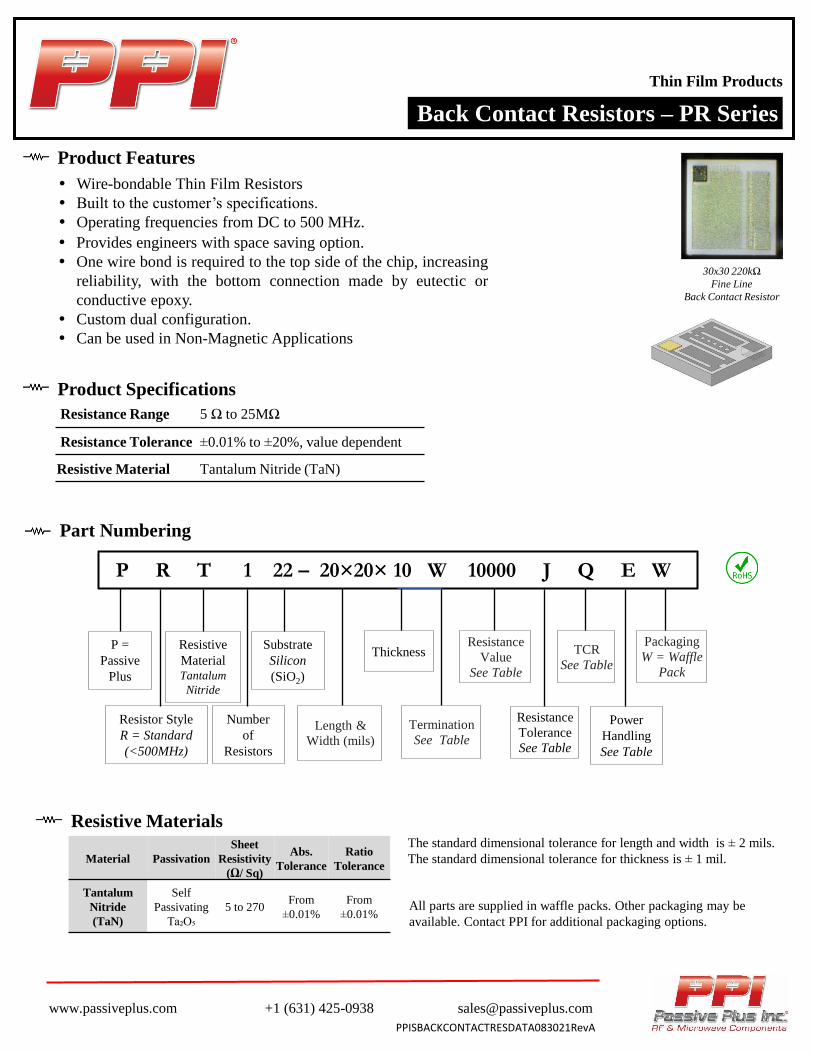
Back Contact Resistors – PR Series
Thin Film Products
www.passiveplus.com +1 (631) 425-0938 [email protected]
Product Features
Part Numbering
P R T 1 22 – 20×20× 10 W 10000 J Q E W
Length &
Width (mils)
Thickness
Resistance
Tolerance
See Table
TCR
See Table
Termination
See Table
Resistance
Value
See Table
P =
Passive
Plus
PPISBACKCONTACTRESDATA083021RevA
Substrate
Silicon
(SiO2)
Power
Handling
See Table
Number
of
Resistors
Product Specifications
Resistance Range 5 Ω to 25MΩ
Resistance Tolerance ±0.01% to ±20%, value dependent
Resistive Material Tantalum Nitride (TaN)
Resistor Style
R = Standard
(<500MHz)
Resistive
MaterialTantalum
Nitride
Packaging
W = Waffle
Pack
The standard dimensional tolerance for length and width is ± 2 mils.
The standard dimensional tolerance for thickness is ± 1 mil.
All parts are supplied in waffle packs. Other packaging may be
available. Contact PPI for additional packaging options.
Wire-bondable Thin Film Resistors
Built to the customer’s specifications.
Operating frequencies from DC to 500 MHz.
Provides engineers with space saving option.
One wire bond is required to the top side of the chip, increasing
reliability, with the bottom connection made by eutectic or
conductive epoxy.
Custom dual configuration.
Can be used in Non-Magnetic Applications
Resistive Materials
Material Passivation
Sheet
Resistivity
(Ω/ Sq)
Abs.
Tolerance
Ratio
Tolerance
Tantalum
Nitride
(TaN)
Self
Passivating
Ta₂O₅
5 to 270From
±0.01%
From
±0.01%
30x30 220kΩ
Fine Line
Back Contact Resistor

www.passiveplus.com +1 (631) 425-0938 [email protected]
Thin Film Products
Substrate Materials
Tolerance B D F G H J K L M Q S
Code ± 0.1% ± 0.5% ± 1% ± 2% ± 3% ± 5% ± 10% ± 15% ± 20% ± 0.05% ± 0.01%
Resistance Tolerance Codes
Terminations Power Handling Codes
Temperature Coefficient of Resistance
* Limit of ± 50mΩs
Back Contact Resistors – PR Series
Metallization Code
Top Side Bottom Side
TaN/Pd/Au Au W
Watts Code Watts Code
50 mW C 250 Mw G
75 mW D 350 mW M
100 mW E 400 mW R
125 Mw I 500 mW H
150 mW F 750 mW J
200 mW O 1.0 W K
Material Thickness Surface Finish
Dielectric
Constant
(@ 1MHz)
Coefficient of
Thermal Expansion
(x 10⁶/ °C)
Thermal
Conductivity
(W/m*K)
Code
Silicon (Si)
(with 12kÅ SiO₂)0.005" - 0.010" Chemical Polish
N/A
(SiO₂ K=1.38)
2.49 - 4.44
(25°C to < 1000°C)
149
(SiO₂ 1.38)22
Material±150
ppm/°C
±100
ppm/°C
±50
ppm/°C
±25
ppm/°C
±10
ppm/°C
±5
ppm/°C
Tantalum
Nitride
(TaN)
Q V W X Y Z
Standard Yes --- --- --- ---
NiChrome
(NiCr)--- --- Yes Standard Yes Yes
PPISBACKCONTACTRESDATA083021RevA

Power Handling & Standard Resistance Ranges by Material and Case Size
Typical PPI commercial testing includes 100% visual inspection, 100% electrical testing with short time
overload, and TCR sampling.
Our parts meet or exceed additional MIL-PRF-55342 and MIL-STD-202 requirements.
Thin Film Products
www.passiveplus.com +1 (631) 425-0938 [email protected]
Back Contact Resistors – PR Series
Power Handling Resistance Range
Case Size Silicon Min
(Ω )
Max
(Ω )
Silicon (C-22)mils (inches) (C-22)
12 x 9(0.012 x 0.009)
50 mW 1-3 150K
14 x 12(0.014 x 0.012)
100 mW 1-3 200K
20 x 10(0.020 x 0.010)
100 mW 1-3 250K
15 x 15(0.015 x 0.015)
100 mW 1-2 500K
20 x 20(0.020 x 0.020)
250 mW 1-2 750K
30 x 20(0.030 x 0.020)
250 mW 1-2 1M
40 x 20(0.040 x 0.020)
250 mW 1-2 1.5M
30 x 30(0.030 x 0.030)
250 mW 1-2 2M
35 x 35(0.035 x 0.035)
250 mW 1-2 3M
40 x 40(0.040 x 0.040)
350 mW 1-2 5M
50 x 25(0.050 x 0.025)
350 mW 1-2 3M
60 x 30(0.060 x 0.030)
500 mW 1-2 6M
50 x 50(0.050 x 0.050)
500 mW 1-2 7M
60 x 60(0.060 x 0.060)
500 mW 1-2 15M
80 x 50(0.080 x 0.050)
500 mW 1-2 20M
100 x 50(0.100 x 0.050)
500 mW 1-2 25M
120 x 60(0.120 x 0.060)
750 mW 1-2 30M
100 x 100(0.100 x 0.100)
750 mW 1-2 35M
PPISBACKCONTACTRESDATA083021RevA

General Properties
Operating Temperature -55°C to +150°C
Storage Temperature -65°C to +150°C
Operating Frequency DC to 500 MHz
Voltage Rating 100V maximum
Power Derating
(See Chart at Right)
Full power up to 70°C
Derated linearly to zero power at 150°C
Testing Performed Specification / Standard
Visual InspectionMIL-PRF-55342
MIL-STD-883
Mechanical Inspection MIL-PRF-55342
DC ResistanceMIL-PRF-55342
MIL-STD-202
Resistance Temperature Characteristics (TCR) MIL-PRF-55342
Short Time Overload MIL-PRF-55342
High Temperature Exposure MIL-PRF-55342
Thermal ShockMIL-PRF-55342
MIL-STD-202
Resistance to Bonding Exposure MIL-PRF-55342
Wire Bonding Integrity MIL-PRF-55342
Life TestMIL-PRF-55342
MIL-STD-202
Testing
PackagingESD waffle packs are standard. Film rings and gel pack packaging are available upon request.
Higher power ratings, additional sizes, and custom resistors available. Please contact [email protected].
Performance Specifications
Thin Film Products
www.passiveplus.com +1 (631) 425-0938 [email protected]
Back Contact Resistors – PR Series
PPISBACKCONTACTRESDATA083021RevA

Standard Edge Wrapped Chip Resistors – PR Series
Thin Film Products
www.passiveplus.com +1 (631) 425-0938 [email protected]
Product Features
Part Numbering
P R T 1 28 – 40×20× 10 N 200R0 G Q K W
Length &
Width (mils)
Thickness
Resistance
Tolerance
See Table
TCR
See Table
Termination
See Table
Resistance
Value
See Table
P =
Passive
Plus
PPISTDRESISTOREDGEDATA083021RevA
Substrate
See Table
Power
Handling
See Table
Number
of
Resistors
Product Specifications
Resistance Range 1 Ω to 3.5MΩ
Resistance Tolerance ±0.01% to ±20%, value dependent
Resistor Style
R = Standard
(<500MHz)
Resistive
Material
See Table
Packaging
W = Waffle
Pack
The standard dimensional tolerance for length and width is ± 2 mils.
The standard dimensional tolerance for thickness is ± 1 mil.
Resistive Materials
Material Passivation
Sheet
Resistivity
(Ω/ Sq)
Abs.
Tolerance
Ratio
Tolerance
Tantalum
Nitride
(TaN)
Self
Passivating
Ta₂O₅
5 to 270From
±0.01%
From
±0.01%
NiChrome
(NiCr)SiO₂ 5 to 250
From
±0.01%
From
±0.01%
All parts are supplied in waffle packs. Other packaging may be available.
Contact PPI for additional packaging options.
Half Wrap Full Wrap
20x10 392Ω
Full Wrap Resistor
Half wrap style chips have solid gold back contiguous with one pad, therefore
eliminating one wirebond
Full wrap style chips have both pads continue to the back side, allowing
elimination of all wirebonds
Can be used in Non-Magnetic Applications
Example shown below: Standard Resistor, TaN resistive element, AlN substrate, case size 0.040”
× 0.020” × 0.010”, dual edge wrap, resistance 200Ω ± 2%, 150 ppm TCR, 1.0 W max power
handling.

www.passiveplus.com +1 (631) 425-0938 [email protected]
Thin Film Products
Material Thickness Surface
Finish
Dielectric
Constant
(@ 1MHz)
Coefficient of
Thermal Expansion
(x 10⁶/ °C)
Thermal
Conductivity
(W/m*K)
Code
Alumina
(Al₂O₃)0.005" - 0.010" 2µ" - 3µ" 9.9
7
(25°C to < 300°C)26.9 35
Aluminum Nitride
(AlN)0.005" - 0.010" 6µ“ - 8µ" 8.0 – 9.1
4.6 - 5.7
(25°C to < 1000°C)170 28
Beryllium Oxide
(BeO)0.005" - 0.010" < 5µ" 6.76
9
(25°C to < 1000°C)285 25
Substrate Materials
Tolerance B D F G H J K L M Q S
Code ± 0.1% ± 0.5% ± 1% ± 2% ± 3% ± 5% ± 10% ± 15% ± 20% ± 0.05% ± 0.01%
Resistance Tolerance Codes
Terminations Power Handling Codes
Watts Code Watts Code
50 mW C 750 mW J
75 mW D 1.0 W K
100 mW E 1.4 W U
125 mW I 2.0 W L
150 mW F 2.8 W Y
200 mW O 3.0 W N
250 mW G 4.0 W P
350 mW M 5.0 W Q
400 mW R 6.0 W 2
500 mW H 10 W S
Temperature Coefficient of Resistance
* Limit of ± 50mΩs
Description Code Application Metallization
1 Side Wrap H Epoxy or Au/Sn Ta/Pd/Au
1 Side Wrap MEpoxy, Au/Sn or
Sn SolderTiW/Ni/Au
1 Side Wrap S Sn Solder Ball TiW/Ni/Au - solder dipped
2 Side Wrap J Epoxy or Au/Sn Ta/Pd/Au
2 Side Wrap NEpoxy, Au/Sn or
Sn SolderTiW/Ni/Au
2 Side Wrap T Sn Solder Ball TiW/Ni/Au - solder dipped
Material±150
ppm/°C
±100
ppm/°C
±50
ppm/°C
±25
ppm/°C
±10
ppm/°C
±5
ppm/°C
Tantalum
Nitride
(TaN)
Q V W X Y Z
Standard Yes --- --- --- ---
NiChrome
(NiCr)--- --- Yes Standard Yes Yes
Standard Edge Wrapped Chip Resistors – PR Series
PPISTDRESISTOREDGEDATA083021RevA

Power Handling & Standard Resistance Ranges by Material and Case Size
Power Handling Resistance Range
Case Size Alumina Silicon AlN BeO Quartz
Min
(Ω )
Max
(Ω )
Alumina
(C-35)
Max
(Ω )
Silicon
(C-22)
Max
(Ω )
AlN
(C-28)
Max
(Ω )
BeO
(C-25)
Max
(Ω )
Quartz
(C-20)
mils
(inches) (C35) (C-22) (C-28) (C-25) (C-20)
12 x 9(0.012 x 0.009)
50 mW 50 mW 200 mW 400 mW 10 mW 1-3 25K 150K 25K 25K 150K
14 x 12(0.014 x 0.012)
100 mW 100 mW 400 mW 750 mW 20 mW 1-3 40K 200K 40K 40K 200K
20 x 10(0.020 x 0.010)
100 mW 100 mW 400 mW 750 mW 20 mW 1-3 60K 250K 60K 60K 250K
15 x 15(0.015 x 0.015)
100 mW 100 mW 400 mW 750 mW 20 mW 1-2 70K 500K 70K 70K 500K
20 x 20(0.020 x 0.020)
250 mW 250 mW 1.0 W 2.0 W 50 mW 1-2 125K 750K 125K 125K 750K
30 x 20(0.030 x 0.020)
250 mW 250 mW 1.0 W 2.0 W 50 mW 1-2 200K 1M 200K 200K 1M
40 x 20(0.040 x 0.020)
250 mW 250 mW 1.0 W 2.0 W 50 mW 1-2 250K 1.5M 250K 250K 1.5M
30 x 30(0.030 x 0.030)
250 mW 250 mW 1.0 W 2.0 W 50 mW 1-2 275K 2M 275K 275K 2M
35 x 35(0.035 x 0.035)
250 mW 250 mW 1.0 W 2.0 W 50 mW 1-2 300K 3M 300K 300K 3M
40 x 40(0.040 x 0.040)
350 mW 350 mW 1.4 W 2.8 W 70 mW 1-2 500K 5M 500K 500K 5M
50 x 25(0.050 x 0.025)
350 mW 350 mW 1.4 W 2.8 W 70 mW 1-2 300K 3M 300K 300K 3M
60 x 30(0.060 x 0.030)
500 mW 500 mW 2.0 W 4.0 W 100 mW 1-2 500K 6M 500K 500K 6M
50 x 50(0.050 x 0.050)
500 mW 500 mW 2.0 W 4.0 W 100 mW 1-2 700K 7M 700K 700K 7M
60 x 60(0.060 x 0.060)
500 mW 500 mW 2.0 W 4.0 W 100 mW 1-2 2M 15M 2M 2M 15M
80 x 50(0.080 x 0.050)
500 mW 500 mW 2.0 W 4.0 W 100 mW 1-2 2M 20M 2M 2M 20M
100 x 50(0.100 x 0.050)
500 mW 500 mW 2.0 W 4.0 W 100 mW 1-2 2.5M 25M 2.5M 2.5M 25M
120 x 60(0.120 x 0.060)
750 mW 750 mW 3.0 W 6.0 W 125 mW 1-2 3M 30M 3M 3M 30M
100 x 100(0.100 x 0.100)
750 mW 750 mW 3.0 W 6.0 W 125 mW 1-2 3.5M 35M 3.5M 3.5M 35M
Typical PPI commercial testing includes 100% visual inspection, 100% electrical testing with short time
overload, and TCR sampling.
Our parts meet or exceed additional MIL-PRF-55342 and MIL-STD-202 requirements.
Thin Film Products
www.passiveplus.com +1 (631) 425-0938 [email protected]
Standard Edge Wrapped Chip Resistors – PR Series
PPISTDRESISTOREDGEDATA083021RevA

General Properties
Operating Temperature -55°C to +150°C
Storage Temperature -65°C to +150°C
Operating Frequency DC to 500 MHz
Voltage Rating 100V maximum
Power Derating
(See Chart at Right)
Full power up to 70°C
Derated linearly to zero power at 150°C
Testing Performed Specification / Standard
Visual InspectionMIL-PRF-55342
MIL-STD-883
Mechanical Inspection MIL-PRF-55342
DC ResistanceMIL-PRF-55342
MIL-STD-202
Resistance Temperature Characteristics (TCR) MIL-PRF-55342
Short Time Overload MIL-PRF-55342
High Temperature Exposure MIL-PRF-55342
Thermal ShockMIL-PRF-55342
MIL-STD-202
Resistance to Bonding Exposure MIL-PRF-55342
Wire Bonding Integrity MIL-PRF-55342
Life TestMIL-PRF-55342
MIL-STD-202
Testing
PackagingESD waffle packs are standard. Film rings and gel pack packaging are available upon request.
Higher power ratings, additional sizes, and custom resistors available. Please contact [email protected].
Performance Specifications
Thin Film Products
www.passiveplus.com +1 (631) 425-0938 [email protected]
Standard Edge Wrapped Chip Resistors – PR Series
PPISTDRESISTOREDGEDATA083021RevA

Microwave Chip Resistors – PM Series
Thin Film Products
www.passiveplus.com +1 (631) 425-0938 [email protected]
Product Features
Part Numbering
P M T 1 35 – 20×20× 10 A 10000 J Q E W
Length &
Width (mils)
Thickness
Resistance
Tolerance
See Table
TCR
See Table
Termination
See Table
Resistance
Value
See Table
P =
Passive
Plus
PPIMICROWAVERESDATA083021RevA
Substrate
See Table
Power
Handling
See Table
Number
of
Resistors
Product Specifications
Resistance Range 2 Ω to 5kΩ
Resistance
Tolerance±0.01% to ±20%, value dependent
VSWR DC to 10 GHz 10 to 20 GHz 20 to 60 GHZ
1.2:1 1.3:1 1.5:1
Resistor Style
M =
Microwave
Resistive
Material
See Table
Packaging
W = Waffle
Pack
The standard dimensional tolerance for length and width is ± 2 mils.
The standard dimensional tolerance for thickness is ± 1 mil.
Resistive Materials
Material Passivation
Sheet
Resistivity
(Ω/ Sq)
Abs.
Tolerance
Ratio
Tolerance
Tantalum
Nitride
(TaN)
Self
Passivating
Ta₂O₅
5 to 270From
±0.01%
From
±0.01%
NiChrome
(NiCr)SiO₂ 5 to 250
From
±0.01%
From
±0.01%
All parts are supplied in waffle packs. Other packaging may be
available. Contact PPI for additional packaging options.
Special microwave laser-trimming to ensure a tight tolerance at high frequencies
Compatible with flip-chip configurations
Operating frequencies up to 60 GHz; higher frequencies are available
Can be used in Non-Magnetic Applications
Example shown: Microwave Resistor, TaN resistive element, alumina substrate, case size 0.020” × 0.020” × 0.010”, PdAu bonding pad,
bottom side bare, resistance 1000 Ω ± 5%, 150 ppm TCR, microwave trim, 100 mW max power handling.

www.passiveplus.com +1 (631) 425-0938 [email protected]
Thin Film Products
Substrate Materials
Tolerance B D F G H J K L M Q S
Code ± 0.1% ± 0.5% ± 1% ± 2% ± 3% ± 5% ± 10% ± 15% ± 20% ± 0.05% ± 0.01%
Resistance Tolerance Codes
Terminations
Power Handling Codes
Temperature Coefficient of Resistance
Microwave Chip Resistors – PM Series
Material Thickness Surface Finish
Dielectric
Constant
(@ 1MHz)
Coefficient of
Thermal Expansion
(x 10⁶/ °C)
Thermal
Conductivity
(W/m*K)
Code
Alumina
(Al₂O₃)0.005" - 0.010" 2µ" - 3µ" 9.9
7
(25°C to < 300°C)26.9 35
Aluminum Nitride
(AlN)0.005" - 0.010" 6µ“ - 8µ" 8.0 – 9.1
4.6 - 5.7
(25°C to < 1000°C)170 28
Beryllium Oxide
(BeO)0.005" - 0.010" < 5µ" 6.76
9
(25°C to < 1000°C)285 25
Quartz
(Fused Silica)0.005" - 0.010"
60/40
Optical Polish3.826
0.55
(25°C to < 300°C)1.38 20
Metallization Code
Top Side Bottom Side
Pd / Au A
Flip Chip
(Ti/Pt/Au)R
Pd/Au Ta/Pd/Au D
Watts Code Watts Code Watts Code
10 mW A 350 mW M 4.0 W P
20 mW B 400 mW R 5.0 W Q
50 mW C 500 mW H 6.0 W Z
75 mW D 750 mW J 10 W S
100 mW E 1.0 W K 15 W T
125 mW I 1.4 W U 20 W V
150 mW F 2.0 W L 25 W W
200 mW O 2.8 W Y 30 W Z
250 mW G 3.0 W N 50 W X
40 W 1
Material±150
ppm/°C
±100
ppm/°C
±50
ppm/°C
±25
ppm/°C
±10
ppm/°C
±5
ppm/°C
Tantalum
Nitride
(TaN)
Q V W X Y Z
Standard Yes --- --- --- ---
NiChrome
(NiCr)--- --- Yes Standard Yes Yes
PPIMICROWAVERESDATA083021RevA

Power Handling & Standard Resistance Ranges by Material and Case Size
Typical PPI commercial testing includes 100% visual inspection, 100% electrical testing with short time
overload, and TCR sampling.
Our parts meet or exceed additional MIL-PRF-55342 and MIL-STD-202 requirements.
Thin Film Products
www.passiveplus.com +1 (631) 425-0938 [email protected]
Microwave Chip Resistors – PM Series
Standard Power Handling High Power Resistor Range
Case Size Alumina AlN BeO Quartz
Min
(Ω )
Max
(Ω)
Min
(Ω)
Max
(Ω)
Max
(Ω )
Alumina
(C-35)
Max
(Ω )
AlN
(C-28)
Max
(Ω )
BeO
(C-25)
mils
(inches) (C35) (C-28) (C-25) (C-20)
12 x 9(0.012 x 0.009)
50 mW 200 mW 400 mW 10 mW 4 500 --- --- --- --- ---
14 x 12(0.014 x 0.012)
100 mW 400 mW 750 mW 20 mW 3 750 --- --- --- --- ---
20 x 10(0.020 x 0.010)
100 mW 400 mW 750 mW 20 mW 3 1000 2 1000 250 mW 1.0 W 2.0 W
15 x 15(0.015 x 0.015)
100 mW 400 mW 750 mW 20 mW 4 1000 2 1000 250 mW 1.0 W 2.0 W
20 x 20(0.020 x 0.020)
250 mW 1.0 W 2.0 W 50 mW 2 1250 2 1000 500 mW 2.0 W 4.0 W
30 x 20(0.030 x 0.020)
250 mW 1.0 W 2.0 W 50 mW 2 2500 2 1000 500 mW 2.0 W 4.0 W
40 x 20(0.040 x 0.020)
250 mW 1.0 W 2.0 W 50 mW 2 3750 2 1000 750 mW 3.0 W 6.0 W
30 x 30(0.030 x 0.030)
250 mW 1.0 W 2.0 W 50 mW 2 2500 2 1000 750 mW 2.0 W 6.0 W
35 x 35(0.035 x 0.035)
250 mW 1.0 W 2.0 W 50 mW 2 3000 2 1000 1.0 W 4.0 W 6.0 W
40 x 40(0.040 x 0.040)
350 mW 1.4 W 2.8 W 70 mW 2 3750 2 1000 1.0 W 4.0 W 6.0 W
50 x 25(0.050 x 0.025)
350 mW 1.4 W 2.8 W 70 mW 3 5000 2 1000 1.0 W 4.0 W 6.0 W
60 x 30(0.060 x 0.030)
500 mW 2.0 W 4.0 W 100 mW 3 5000 2 1000 1.4 W 5.0 W 10.0 W
50 x 50(0.050 x 0.050)
500 mW 2.0 W 4.0 W 100 mW 2 5000 2 1000 1.4 W 5.0 W 10.0 W
60 x 60(0.060 x 0.060)
500 mW 2.0 W 4.0 W 100 mW 2 5000 2 1000 1.4 W 5.0 W 10.0 W
80 x 50(0.080 x 0.050)
500 mW 2.0 W 4.0 W 100 mW 2 5000 2 1000 2.8 W 10.0 W 15.0 W
100 x 50(0.100 x 0.050)
500 mW 2.0 W 4.0 W 100 mW 2 5000 2 1000 2.8 W 10.0 W 15.0 W
120 x 60(0.120 x 0.060)
750 mW 3.0 W 6.0 W 125 mW 2 5000 2 1000 2.8 W 10.0 W 15.0W
100 x 100(0.100 x 0.100)
750 mW 3.0 W 6.0 W 125 mW 2 5000 2 1000 2.8 W 10.0 W 15.0 W
PPIMICROWAVERESDATA083021RevA

General Properties
Operating Temperature -55°C to +150°C
Storage Temperature -65°C to +150°C
Operating Frequency DC to 500 MHz
Voltage Rating 100V maximum
Power Derating
(See Chart at Right)
Full power up to 70°C
Derated linearly to zero power at 150°C
Testing Performed Specification / Standard
Visual InspectionMIL-PRF-55342
MIL-STD-883
Mechanical Inspection MIL-PRF-55342
DC ResistanceMIL-PRF-55342
MIL-STD-202
Resistance Temperature Characteristics (TCR) MIL-PRF-55342
Short Time Overload MIL-PRF-55342
High Temperature Exposure MIL-PRF-55342
Thermal ShockMIL-PRF-55342
MIL-STD-202
Resistance to Bonding Exposure MIL-PRF-55342
Wire Bonding Integrity MIL-PRF-55342
Life TestMIL-PRF-55342
MIL-STD-202
Testing
Packaging
ESD waffle packs are standard. Film rings and gel pack packaging are available upon request.
Higher power ratings, additional sizes, and custom resistors available. Please contact [email protected].
Performance Specifications
Thin Film Products
www.passiveplus.com +1 (631) 425-0938 [email protected]
Microwave Chip Resistors – PM Series
PPIMICROWAVERESDATA083021RevA

Microwave Edge Wrapped Chip Resistors
Thin Film Products
www.passiveplus.com +1 (631) 425-0938 [email protected]
Product Features
Part Numbering
P M T 1 28 – 40×20× 10 N 200R0 G Q K W
Length &
Width (mils)
Thickness
Resistance
Tolerance
See Table
TCR
See Table
Termination
See Table
Resistance
Value
See Table
P =
Passive
Plus
PPIMICROWAVERESEDGEDATA083021RevA
Substrate
See Table
Power
Handling
See Table
Number
of
Resistors
Product Specifications
Resistance Range 2 Ω to 5kΩ
Resistance
Tolerance±0.5% to ±20%, value dependent
Resistor Style
M =
Microwave
Resistive
Material
See Table
Packaging
W = Waffle
Pack
The standard dimensional tolerance for length and width is ± 2 mils.
The standard dimensional tolerance for thickness is ± 1 mil.
Resistive Materials
Material Passivation
Sheet
Resistivity
(Ω/ Sq)
Abs.
Tolerance
Ratio
Tolerance
Tantalum
Nitride
(TaN)
Self
Passivating
Ta₂O₅
5 to 270From
±0.01%
From
±0.01%
NiChrome
(NiCr)SiO₂ 5 to 250
From
±0.01%
From
±0.01%
All parts are supplied in waffle packs. Other packaging may be
available. Contact PPI for additional packaging options.
Half Wrap Full Wrap
• Edge Wrap similar in construction to our standard surface mount
wrap resistors, with half wrap and full wrap styles available.
• The addition of a microwave design allows for operation at
frequencies up to 60 GHz.
• Can be used in Non-Magnetic Applications
Example shown below: Microwave Resistor, TaN resistive element, AlN substrate, case size 0.040” × 0.020” × 0.010”, dual edge wrap, resistance 200 Ω ± 2%, 150 ppm TCR, 1.0 W max power handling.

www.passiveplus.com +1 (631) 425-0938 [email protected]
Thin Film Products
Substrate Materials
Tolerance B D F G H J K L M Q S
Code ± 0.1% ± 0.5% ± 1% ± 2% ± 3% ± 5% ± 10% ± 15% ± 20% ± 0.05% ± 0.01%
Resistance Tolerance Codes
Terminations
Power Handling Codes
Temperature Coefficient of Resistance
Material Thickness Surface Finish
Dielectric
Constant
(@ 1MHz)
Coefficient of
Thermal Expansion
(x 10⁶/ °C)
Thermal
Conductivity
(W/m*K)
Code
Alumina
(Al₂O₃)0.005" - 0.010" 2µ" - 3µ" 9.9
7
(25°C to < 300°C)26.9 35
Aluminum Nitride
(AlN)0.005" - 0.010" 6µ“ - 8µ" 8.0 – 9.1
4.6 - 5.7
(25°C to < 1000°C)170 28
Beryllium Oxide
(BeO)0.005" - 0.010" < 5µ" 6.76
9
(25°C to < 1000°C)285 25
Watts Code Watts Code Watts Code
10 mW A 350 mW M 4.0 W P
20 mW B 400 mW R 5.0 W Q
50 mW C 500 mW H 6.0 W Z
75 mW D 750 mW J 10 W S
100 mW E 1.0 W K 15 W T
125 mW I 1.4 W U 20 W V
150 mW F 2.0 W L 25 W W
200 mW O 2.8 W Y 30 W Z
250 mW G 3.0 W N 50 W X
40 W 1
Metallization Application Code
1 Side Wrap Epoxy or Au/Sn H
1 Side Wrap Epoxy, Au/Sn, or Sn Solder M
1 Side Wrap Sn Solder Ball S
2 Side Wrap Epoxy or Au/Sn J
2 Side Wrap Epoxy, Au/Sn, or Sn Solder N
2 Side Wrap Sn Solder Ball T
Material±150
ppm/°C
±100
ppm/°C
±50
ppm/°C
±25
ppm/°C
±10
ppm/°C
±5
ppm/°C
Tantalum
Nitride
(TaN)
Q V W X Y Z
Standard Yes --- --- --- ---
NiChrome
(NiCr)--- --- Yes Standard Yes Yes
Microwave Edge Wrapped Chip Resistors
PPIMICROWAVERESEDGEDATA083021RevA

Power Handling & Standard Resistance Ranges by Material and Case Size
Typical PPI commercial testing includes 100% visual inspection, 100% electrical testing with short time
overload, and TCR sampling.
Our parts meet or exceed additional MIL-PRF-55342 and MIL-STD-202 requirements.
Thin Film Products
www.passiveplus.com +1 (631) 425-0938 [email protected]
Standard Power Handling High Power Resistor Range
Case Size Alumina AlN BeO Quartz
Min
(Ω )
Max
(Ω)
Min
(Ω)
Max
(Ω)
Max
(Ω )
Alumina
(C-35)
Max
(Ω )
AlN
(C-28)
Max
(Ω )
BeO
(C-25)
mils
(inches) (C35) (C-28) (C-25) (C-20)
12 x 9(0.012 x 0.009)
50 mW 200 mW 400 mW 10 mW 4 500 --- --- --- --- ---
14 x 12(0.014 x 0.012)
100 mW 400 mW 750 mW 20 mW 3 750 --- --- --- --- ---
20 x 10(0.020 x 0.010)
100 mW 400 mW 750 mW 20 mW 3 1000 2 1000 250 mW 1.0 W 2.0 W
15 x 15(0.015 x 0.015)
100 mW 400 mW 750 mW 20 mW 4 1000 2 1000 250 mW 1.0 W 2.0 W
20 x 20(0.020 x 0.020)
250 mW 1.0 W 2.0 W 50 mW 2 1250 2 1000 500 mW 2.0 W 4.0 W
30 x 20(0.030 x 0.020)
250 mW 1.0 W 2.0 W 50 mW 2 2500 2 1000 500 mW 2.0 W 4.0 W
40 x 20(0.040 x 0.020)
250 mW 1.0 W 2.0 W 50 mW 2 3750 2 1000 750 mW 3.0 W 6.0 W
30 x 30(0.030 x 0.030)
250 mW 1.0 W 2.0 W 50 mW 2 2500 2 1000 750 mW 2.0 W 6.0 W
35 x 35(0.035 x 0.035)
250 mW 1.0 W 2.0 W 50 mW 2 3000 2 1000 1.0 W 4.0 W 6.0 W
40 x 40(0.040 x 0.040)
350 mW 1.4 W 2.8 W 70 mW 2 3750 2 1000 1.0 W 4.0 W 6.0 W
50 x 25(0.050 x 0.025)
350 mW 1.4 W 2.8 W 70 mW 3 5000 2 1000 1.0 W 4.0 W 6.0 W
60 x 30(0.060 x 0.030)
500 mW 2.0 W 4.0 W 100 mW 3 5000 2 1000 1.4 W 5.0 W 10.0 W
50 x 50(0.050 x 0.050)
500 mW 2.0 W 4.0 W 100 mW 2 5000 2 1000 1.4 W 5.0 W 10.0 W
60 x 60(0.060 x 0.060)
500 mW 2.0 W 4.0 W 100 mW 2 5000 2 1000 1.4 W 5.0 W 10.0 W
80 x 50(0.080 x 0.050)
500 mW 2.0 W 4.0 W 100 mW 2 5000 2 1000 2.8 W 10.0 W 15.0 W
100 x 50(0.100 x 0.050)
500 mW 2.0 W 4.0 W 100 mW 2 5000 2 1000 2.8 W 10.0 W 15.0 W
120 x 60(0.120 x 0.060)
750 mW 3.0 W 6.0 W 125 mW 2 5000 2 1000 2.8 W 10.0 W 15.0W
100 x 100(0.100 x 0.100)
750 mW 3.0 W 6.0 W 125 mW 2 5000 2 1000 2.8 W 10.0 W 15.0 W
Microwave Edge Wrapped Chip Resistors
PPIMICROWAVERESEDGEDATA083021RevA

General Properties
Operating Temperature -55°C to +150°C
Storage Temperature -65°C to +150°C
Operating Frequency DC to 500 MHz
Voltage Rating 100V maximum
Power Derating
(See Chart at Right)
Full power up to 70°C
Derated linearly to zero power at 150°C
Testing Performed Specification / Standard
Visual InspectionMIL-PRF-55342
MIL-STD-883
Mechanical Inspection MIL-PRF-55342
DC ResistanceMIL-PRF-55342
MIL-STD-202
Resistance Temperature Characteristics (TCR) MIL-PRF-55342
Short Time Overload MIL-PRF-55342
High Temperature Exposure MIL-PRF-55342
Thermal ShockMIL-PRF-55342
MIL-STD-202
Resistance to Bonding Exposure MIL-PRF-55342
Wire Bonding Integrity MIL-PRF-55342
Life TestMIL-PRF-55342
MIL-STD-202
Testing
PackagingESD waffle packs are standard. Film rings and gel pack packaging are available upon request.
Higher power ratings, additional sizes, and custom resistors available. Please contact [email protected].
Performance Specifications
Thin Film Products
www.passiveplus.com +1 (631) 425-0938 [email protected]
Microwave Edge Wrapped Chip Resistors
PPIMICROWAVERESEDGEDATA083021RevA

Dual Chip Resistors – PD Series
Thin Film Products
www.passiveplus.com +1 (631) 425-0938 [email protected]
Product Features
Part Numbering
P D T – 35 – 30×30 – 10000–20000 – A J Q K
Length &
Width (mils)
Resistance
Tolerance
See Table
TCR
See Table
Termination
See Table
Resistance
for First & Second
Resistors
P =
Passive
Plus
PPIDUALCHIPRESDATA083021RevA
Resistance
Ratio
Substrate
See Table
Product Specifications
Resistor Style
See Table
Resistive
Material
See Table
Resistive Style
Code Style
D Dual Resistors
I Isolated Resistors
• Two resistors on a single chip area.
• Available styles are common or isolated node.
• The nature of this design lends itself to tightly matched TCR and electrical
tolerance, with resistance ratios within 0.01% possible (value dependent).
• Can be used in Non-Magnetic Applications
Isolated Node
Configuration
Common Node
Configuration
Resistance Range 2Ω - 1MΩ per resistor (Silicon or Quartz)
2Ω - 160kΩ per resistor (Al₂O₃, BeO, or AlN)
Resistance
Tolerance±0.01% to ±20% value dependent
Standard Size30 mil x 30 mil x 10 mil
0.03” x 0.03” x 0.01”
Resistive Materials
Material Passivation
Sheet
Resistivity
(Ω/ Sq)
Abs.
Tolerance
Ratio
Tolerance
Tantalum
Nitride
(TaN)
Self
Passivating
Ta₂O₅
5 to 270From
±0.01%
From
±0.01%
NiChrome
(NiCr)SiO₂ 5 to 250
From
±0.01%
From
±0.01%
All parts are supplied in waffle packs. Other packaging may be
available. Contact PPI for additional packaging options.

www.passiveplus.com +1 (631) 425-0938 [email protected]
Thin Film Products
Substrate Materials
Tolerance B D F G H J K L M Q S
Code ± 0.1% ± 0.5% ± 1% ± 2% ± 3% ± 5% ± 10% ± 15% ± 20% ± 0.05% ± 0.01%
Resistance Tolerance Codes
Terminations
Power Handling Range by Material
Temperature Coefficient of Resistance
Dual Chip Resistors – PD Series
Material Thickness Surface
Finish
Dielectric
Constant
(@ 1MHz)
Coefficient of
Thermal
Expansion
(x 10⁶/ °C)
Thermal
Conductivity
(W/m*K)
CodePower per
Resistor
Alumina
(Al₂O₃)0.005" - 0.010" 2µ" - 3µ" 9.9
7
(25°C to < 300°C)26.9 35 125 mW
Aluminum
Nitride (AlN)0.005" - 0.010" 6µ“ - 8µ" 8.0 – 9.1
4.6 - 5.7
(25°C to < 1000°C)170 28 500 mW
Beryllium Oxide
(BeO)0.005" - 0.010" < 5µ" 6.76
9
(25°C to < 1000°C)285 25 1 W
Silicon (Si)
(with 12kÅ SiO₂)0.005" - 0.010"
Chemical
Polish
N/A
(SiO₂ K=1.38)
2.49 - 4.44
(25°C to < 1000°C)
149
(SiO₂ 1.38)22 125 mW
Quartz
(Fused Silica)0.005" - 0.010"
60/40
Optical Polish3.826
0.55
(25°C to < 300°C)1.38 20 25 mW
Metallization Code
Top Side Bottom Side
Pd / Au A
Pd / Au Ta/Pd/Au D
Pd/ Au Au Sputtered K
Material±150
ppm/°C
±100
ppm/°C
±50
ppm/°C
±25
ppm/°C
±10
ppm/°C
±5
ppm/°C
Tantalum
Nitride
(TaN)
Q V W X Y Z
Standard Yes --- --- --- ---
NiChrome
(NiCr)--- --- Yes Standard Yes Yes
Case Size Alumina Silicon AlN BeO Quartz
mils
(inches) (C35) (C-22) (C-28) (C-25) (C-20)
30 x 30(0.030 x 0.030)
125 mW 125 mW 500 mW 1.0 W 25 mW
Resistance Ratio Codes
Tolerance To
Other ResistorsCode
±0.01% G
±0.05% H
±0.10% J
±0.25% K
±0.50% M
±1.00% N
No Ratio R
PPIDUALCHIPRESDATA083021RevA
General Properties
Operating Temperature -55°C to +150°C
Storage Temperature -65°C to +150°C
Operating Frequency DC to 500 MHz
Voltage Rating 100V maximum
Power Derating
(See Chart at Right)
Full power up to 70°C
Derated linearly to zero power at 150°C
Testing Performed Specification / Standard
Visual InspectionMIL-PRF-55342
MIL-STD-883
Mechanical Inspection MIL-PRF-55342
DC ResistanceMIL-PRF-55342
MIL-STD-202
Resistance Temperature Characteristics (TCR) MIL-PRF-55342
Short Time Overload MIL-PRF-55342
High Temperature Exposure MIL-PRF-55342
Thermal ShockMIL-PRF-55342
MIL-STD-202
Resistance to Bonding Exposure MIL-PRF-55342
Wire Bonding Integrity MIL-PRF-55342
Life TestMIL-PRF-55342
MIL-STD-202
Testing
Packaging
ESD waffle packs are standard. Film rings and gel pack packaging are available upon request.
Higher power ratings, additional sizes, and custom resistors available. Please contact [email protected].
Performance Specifications
Thin Film Products
www.passiveplus.com +1 (631) 425-0938 [email protected]
Dual Chip Resistors – PD Series
PPIDUALCHIPRESDATA083021RevA
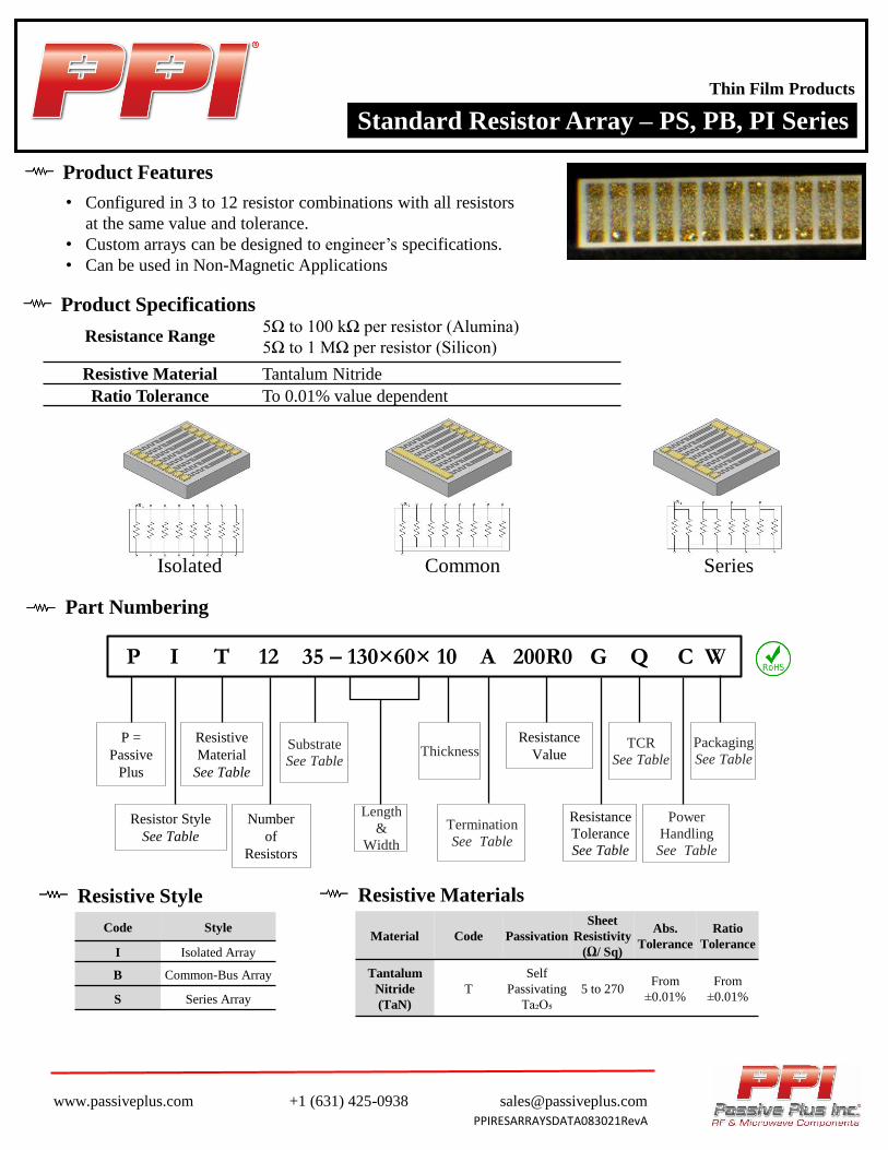
Standard Resistor Array – PS, PB, PI Series
Thin Film Products
www.passiveplus.com +1 (631) 425-0938 [email protected]
Product Features
Part Numbering
P I T 12 35 – 130×60× 10 A 200R0 G Q C W
Substrate
See Table
Resistance
Tolerance
See Table
TCR
See Table
Termination
See Table
Length
&
Width
P =
Passive
Plus
PPIRESARRAYSDATA083021RevA
Resistance
Value
Number
of
Resistors
Resistor Style
See Table
Resistive
Material
See Table
Resistive Style
Code Style
I Isolated Array
B Common-Bus Array
S Series Array
Resistive Materials
Material Code Passivation
Sheet
Resistivity
(Ω/ Sq)
Abs.
Tolerance
Ratio
Tolerance
Tantalum
Nitride
(TaN)
T
Self
Passivating
Ta₂O₅
5 to 270From
±0.01%
From
±0.01%
• Configured in 3 to 12 resistor combinations with all resistors
at the same value and tolerance.
• Custom arrays can be designed to engineer’s specifications.
• Can be used in Non-Magnetic Applications
Isolated Common Series
Thickness
Power
Handling
See Table
Packaging
See Table
Product Specifications
Resistance Range5Ω to 100 kΩ per resistor (Alumina)
5Ω to 1 MΩ per resistor (Silicon)
Resistive Material Tantalum Nitride
Ratio Tolerance To 0.01% value dependent

www.passiveplus.com +1 (631) 425-0938 [email protected]
Thin Film Products
Substrate Materials
Tolerance B D F G H J K L M Q S
Code ± 0.1% ± 0.5% ± 1% ± 2% ± 3% ± 5% ± 10% ± 15% ± 20% ± 0.05% ± 0.01%
Resistance Tolerance Codes
Terminations
Power Handling
Temperature Coefficient of Resistance
Metallization Code
Top Side Bottom Side
Pd / Au A
Pd / Au Ta/Pd/Au D
Pd/ Au Au Sputtered K
Material±150
ppm/°C
±100
ppm/°C
Tantalum
Nitride
(TaN)
Q V
Standard Yes
Recommended Substrates Code
99.6% Alumina (Al₂O₃) 35
Silicon (SiO₂) 20
Resistors 3 4 5 6 7 8 9 10 11 12
Length (mils)40
(0.04")
50
(0.05")
60
(0.06")
70
(0.07")
80
(0.08")
90
(0.09")
100
(0.10")
110
(0.11")
120
(0.12")
130
(0.13")
Width 60 mils (0.06") standard
Thickness 10 mils (0.01") standard
Power 50 mW/ Resistor standard
Packaging
Code Style
WWaffle Pack
(Standard)
G Gel Pack
All parts are supplied in waffle packs. Other packaging may be available.
Contact PPI for additional packaging options.
Standard Resistor Array – PS, PB, PI Series
PPIRESARRAYSDATA083021RevA

General Properties
Operating Temperature -55°C to +150°C
Storage Temperature -65°C to +150°C
Operating Frequency DC to 500 MHz
Voltage Rating 100V maximum
Power Derating
(See Chart at Right)
Full power up to 70°C
Derated linearly to zero power at 150°C
Testing Performed Specification / Standard
Visual InspectionMIL-PRF-55342
MIL-STD-883
Mechanical Inspection MIL-PRF-55342
DC ResistanceMIL-PRF-55342
MIL-STD-202
Resistance Temperature Characteristics (TCR) MIL-PRF-55342
Short Time Overload MIL-PRF-55342
High Temperature Exposure MIL-PRF-55342
Thermal ShockMIL-PRF-55342
MIL-STD-202
Resistance to Bonding Exposure MIL-PRF-55342
Wire Bonding Integrity MIL-PRF-55342
Life TestMIL-PRF-55342
MIL-STD-202
Testing
Packaging
ESD waffle packs are standard. Film rings and gel pack packaging are available upon request.
Higher power ratings, additional sizes, and custom resistors available. Please contact [email protected].
Performance Specifications
www.passiveplus.com +1 (631) 425-0938 [email protected]
Standard Resistor ArrayStandard Resistor Array – PS, PB, PI Series
Thin Film Products
PPIRESARRAYSDATA083021RevA
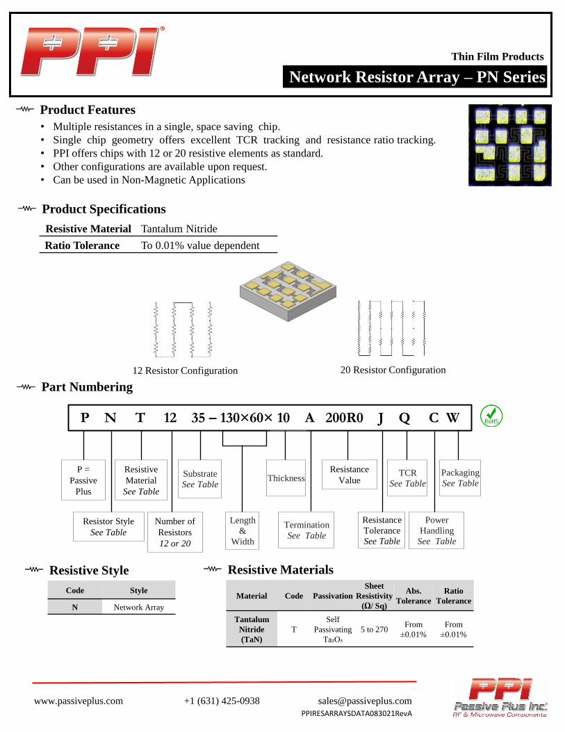
Network Resistor Array – PN Series
Thin Film Products
www.passiveplus.com +1 (631) 425-0938 [email protected]
Product Features
Part Numbering
P N T 12 35 – 130×60× 10 A 200R0 J Q C W
Substrate
See Table
Resistance
Tolerance
See Table
TCR
See Table
Termination
See Table
Length
&
Width
P =
Passive
Plus
Resistance
Value
Number of
Resistors
12 or 20
Resistor Style
See Table
Resistive
Material
See Table
Resistive Style
Code Style
N Network Array
Resistive Materials
Material Code Passivation
Sheet
Resistivity
(Ω/ Sq)
Abs.
Tolerance
Ratio
Tolerance
Tantalum
Nitride
(TaN)
T
Self
Passivating
Ta₂O₅
5 to 270From
±0.01%
From
±0.01%
Thickness
Power
Handling
See Table
Packaging
See Table
Product Specifications
• Multiple resistances in a single, space saving chip.
• Single chip geometry offers excellent TCR tracking and resistance ratio tracking.
• PPI offers chips with 12 or 20 resistive elements as standard.
• Other configurations are available upon request.
• Can be used in Non-Magnetic Applications
12 Resistor Configuration 20 Resistor Configuration
Resistive Material Tantalum Nitride
Ratio Tolerance To 0.01% value dependent
PPIRESARRAYSDATA083021RevA

www.passiveplus.com +1 (631) 425-0938 [email protected]
Thin Film Products
Substrate Materials
Tolerance J K M
Code ± 5% ± 10% ± 20%
Resistance Tolerance Codes
Terminations
Power Handling
Temperature Coefficient of Resistance
Metallization Code
Top Side Bottom Side
Pd / Au A
Pd / Au Ta/Pd/Au D
Pd/ Au Au Sputtered K
Material±150
ppm/°C
±100
ppm/°C
Tantalum
Nitride
(TaN)
Q V
Standard Yes
Packaging
Code Style
WWaffle Pack
(Standard)
G Gel Pack
All parts are supplied in waffle packs. Other packaging may be available.
Contact PPI for additional packaging options.
Material Thickness Surface Finish
Dielectric
Constant
(@ 1MHz)
Coefficient of
Thermal Expansion
(x 10⁶/ °C)
Thermal
Conductivity
(W/m*K)
Code
Alumina
(Al₂O₃)0.005" - 0.010" 2µ" - 3µ" 9.9
7
(25°C to < 300°C)26.9 35
Silicon (Si)
(with 12kÅ SiO₂)0.005" - 0.010" Chemical Polish
N/A
(SiO₂ K=1.38)
2.49 - 4.44
(25°C to < 1000°C)
149
(SiO₂ 1.38)22
Size 30 x 30
(0.030” x 0.030”)
Size 38 x 38
(0.038” x 0.038”)
Resistance Range:
Silicon 80 Ω to 240 kΩ 550Ω to 500 kΩ
Alumina 80 Ω to 50 kΩ 550Ω to 50 kΩ
Resistance DistributionR₁ to R₇ = Rᵼ / 8 R₁ to R₁₀ = Rᵼ / 110
R₈ to R₁₂ = Rᵼ / 40 R₁₁ to R₂₀ = Rᵼ / 11
250mW
Resistance Range
Network Resistor Array – PN Series
PPIRESARRAYSDATA083021RevA

General Properties
Operating Temperature -55°C to +150°C
Storage Temperature -65°C to +150°C
Operating Frequency DC to 500 MHz
Voltage Rating 100V maximum
Power Derating
(See Chart at Right)
Full power up to 70°C
Derated linearly to zero power at 150°C
Testing Performed Specification / Standard
Visual InspectionMIL-PRF-55342
MIL-STD-883
Mechanical Inspection MIL-PRF-55342
DC ResistanceMIL-PRF-55342
MIL-STD-202
Resistance Temperature Characteristics (TCR) MIL-PRF-55342
Short Time Overload MIL-PRF-55342
High Temperature Exposure MIL-PRF-55342
Thermal ShockMIL-PRF-55342
MIL-STD-202
Resistance to Bonding Exposure MIL-PRF-55342
Wire Bonding Integrity MIL-PRF-55342
Life TestMIL-PRF-55342
MIL-STD-202
Testing
PackagingESD waffle packs are standard. Film rings and gel pack packaging are available upon request.
Higher power ratings, additional sizes, and custom resistors available. Please contact [email protected].
Performance Specifications
Thin Film Products
www.passiveplus.com +1 (631) 425-0938 [email protected]
PPIRESARRAYSDATA083021RevA
Network Resistor Array – PN Series

Attenuators – PAT Series
Thin Film Products
www.passiveplus.com +1 (631) 425-0938 [email protected]
Product Features
Part Numbering
P A T S 35 – 50×50× 10 A 3R00 F Q G W
Material
See Table
Attenuation
Tolerance
See Table
TCR
See Table
Bond Pad
Metallization
See Table
Length
&
Width
P =
Passive
Plus
PPIATTENUATORSDATA083021RevA
Attenuation
(dB)
Attenuator
Type
See Table
Attenuator
Resistive
Metallization
See Table
Thickness
Power
Handling
See Table
Packaging
See Table
• Reduces amplitude or power of a signal by a known value. This is
achieved with very little distortion of the signal, maintaining accuracy up to 40 GHz.
• Attenuators are available with or without center Taps
• Single wraps of the ground pad to a full gold backside available
• Additional Attenuator configurations, including balanced attenuators
and triple wrap attenuators, are available as custom parts
• Can be used in Non-Magnetic Applications
Attenuator Top Contact Attenuator, Single Pad Wrap Attenuator, 3-Sided Wrap
Resistive Metallizations
Code Material Passivation
Sheet
Resistivity
(Ω/ Sq)
Abs.
Tolerance
Ratio
Tolerance
T
Tantalum
Nitride
(TaN)
Self
Passivating
Ta₂O₅
5 to 270From
±0.01%
From
±0.01%
Attenuator Type
Code Description
S T-Pattern

www.passiveplus.com +1 (631) 425-0938 [email protected]
Thin Film Products
Materials
Power HandlingTemperature Coefficient of Resistance
Packaging
Code Style
WWaffle Pack
(Standard)
G Gel Pack
All parts are supplied in waffle packs. Other packaging may
be available. Contact PPI for additional packaging options.
Tolerance Code
±0.1dB (-0.5 to -6.0dB) F
±0.2dB (-6.5 to -24.5dB) G
Attenuation Tolerance
Power Code
250mW G
1.0W K
2.0W L
8.0W R
16.0W Y
Power Ratings assume proper
heat sinking is used.TCR Availability Code
±150ppm Standard Q
±100ppm Optional V
Power (W) Value
(LxWxT)
Dimensions (mils)Al₂O₃ AlN BeO Min Max
CODE 35 28 25
50x50x10 250mW 1W 2W 0.5dB 24.5dB
80x60x15 250mW 1W 2W 0.5dB 24.5dB
150x120x25 2W 8W 16W 0.5dB 24.5dB
Metallization Code
Top Only A
Single Wrap, Full GRD Plane M
Flip Chip R
3-sided Wrap X
Bond Pad Metallizations
Attenuators – PAT Series
PPIATTENUATORSDATA083021RevA

General Properties
Operating Temperature -55°C to +150°C
Storage Temperature -65°C to +150°C
Operating Frequency DC to 500 MHz
Voltage Rating 100V maximum
Power Derating
(See Chart at Right)
Full power up to 70°C
Derated linearly to zero power at 150°C
Testing Performed Specification / Standard
Visual InspectionMIL-PRF-55342
MIL-STD-883
Mechanical Inspection MIL-PRF-55342
DC ResistanceMIL-PRF-55342
MIL-STD-202
Resistance Temperature Characteristics (TCR) MIL-PRF-55342
Short Time Overload MIL-PRF-55342
High Temperature Exposure MIL-PRF-55342
Thermal ShockMIL-PRF-55342
MIL-STD-202
Resistance to Bonding Exposure MIL-PRF-55342
Wire Bonding Integrity MIL-PRF-55342
Life TestMIL-PRF-55342
MIL-STD-202
Testing
Packaging
ESD waffle packs are standard. Gel pack packaging also available. Film rings are available upon request for Top
Contact Attenuators only. Please contact PPI for availability.
Higher power ratings, additional sizes, and custom resistors available. Please contact [email protected].
Performance Specifications
Thin Film Products
www.passiveplus.com +1 (631) 425-0938 [email protected]
Attenuators – PAT Series
PPIATTENUATORSDATA083021RevA

Thin Film Products
www.passiveplus.com +1 (631) 425-0938 [email protected]
Product Features
Part Numbering
P TC0 28 100×50×40 N W
Metallization
See Table
Length, Width &
Thickness
See Parts
Characterization
Table
P =
Passive
Plus
PPITHERMALCONDUCTORDATA101321RevA
Material
See Table
Thermal
Conductor
Packaging
See Table
Thermal Conductors – PTC Series
With the increase in heat dissipation from microelectronics devices and the
reduction in overall form factors, thermal management becomes a more and
more important element of electronic product design.
PPI’s Thermal conductors are a passive heat exchanger that transfers the heat
generated by an electronic device to a thermal ground plane or any specific
thermal point where it gets dissipated away from the device.
Our thermal conductors are available in a variety of sizes including standard EIA
case sizes and are constructed using Aluminum Nitride (ALN) or Beryllium
Oxide (BeO).
Product Features
• High Thermal Conductivity
• Low Thermal Resistance
• Low Capacitance
• One piece construction
• RoHS Compliant
• EIA case sizes
• More efficient thermal management
• GaN Power Amplifiers
• High RF Power Amplifiers
• Filters
• Synthesizers
• Switch Mode Power Supplies
• Pin & Laser Diodes
Applications
Functional Applications
• Between active device & adjacent ground planes
• Specific contact pad to case
• Contact pad to contact pad
• Direct component contact to via pad or trace
• Edges fully metalized
Example shown below: Thermal Conductor, AlN, 1005, thickness (40 mils), Platinum/Gold (Pt/Au),
Waffle Pack

www.passiveplus.com +1 (631) 425-0938 [email protected]
Thin Film Products
Parts Characterizations
Packaging
Code Style
WWaffle Pack
(Standard)
G Gel Pack
All parts are supplied in waffle packs. Other packaging may
be available. Contact PPI for additional packaging options.
Metallizations
Termination Code Termination Materials
N* Platinum/Gold (Pt/Au)
X Platinum/Silver (Pt/Ag)
*Recommended
Case Size
Length
(L)
mils / (inches)
Width
(W)
mils / (inches)
Thickness
(T)
mils /
(inches)
Terminal
(t)
Thermal Resistance (°C/W)Thermal Conductivity
(mW/°C)
AlN BeO AlN BeO
030230 ± 2 20 ± 2 20 10
19 12 53 81(.770 ± .051) (.510 ± .0510) (.020 ± .002) -0.25
040240 ± 2 20 ± 2 20 10
25 16 40 61(1.020 ± .051) (.510 ± .0510) (.020 ± .002) -0.25
050550 ± 2 50 ± 2 25 15
10 7 100 153(1.270 ± .051) (1.270 ± .051) (.025 ± .002) -0.38
060360 ± 2 30 ± 2 25 15
20 13 50 76(1.52 ± .051) (.760 ± .051) (.025 ± .002) -0.38
080580 ± 2 50 ± 2 40 20
10 7 100 153(2.030 ± .051) 1.270 ± .051) (.040 ± .002) -0.51
1005100 ± 2 50 ± 2 40 20
13 8 77 122(2.54 ± .051) (1.27 ± .051) (.040 ± .002) -0.51
1020100 ± 2 200 ± 2 40 20
3 2 320 508(2.540 ± .051) (5.080 ± .051) (.040 ± .002) -0.51
1111110 ± 2 110 ± 2 40 20
7 4 153 240(2.790 ± .051) (2.790 ± .051) (.040 ± .002) -0.51
2010195 ± 10 195 ± 10 60 30
10 6 100 159(4.950 ± .254) (2.410 ± .254) (.060 ± .002) -0.77
2525240 ± 10 250 ± 10 60 40
4 3 240 380(6.100 ± .254) (6.350 ± .254) (.060 ± .002) -1.02
3725370 ± 10 245 ± 10 60 50
6 4 160 254(9.400 ± .254) (6.220 ± .254) (.060 ± .002) -1.27
3737365 ± 10 375 ± 10 60 50
4 3 240 380(9.270 ± .254) (9.530 ± .254) (.060 ± .002) -1.27
Thermal Conductors – PTC Series
AlN BeO
CODE 28 25
Materials
PPITHERMALCONDUCTORDATA101321RevA

General Properties
Operating Temperature -55°C to +150°C
Storage Temperature -65°C to +150°C
Insulation Resistance 1012 Ω min at 25°C
Testing Performed Specification / Standard
Visual InspectionMIL-PRF-55342
MIL-STD-883
Mechanical Inspection MIL-PRF-55342
DC ResistanceMIL-PRF-55342
MIL-STD-202
Resistance Temperature Characteristics (TCR) MIL-PRF-55342
Short Time Overload MIL-PRF-55342
High Temperature Exposure MIL-PRF-55342
Thermal ShockMIL-PRF-55342
MIL-STD-202
Resistance to Bonding Exposure MIL-PRF-55342
Wire Bonding Integrity MIL-PRF-55342
Life TestMIL-PRF-55342
MIL-STD-202
Testing
Higher power ratings, additional sizes, and custom resistors available. Please contact [email protected].
Performance Specifications
Thin Film Products
www.passiveplus.com +1 (631) 425-0938 [email protected]
Thermal Conductors – PTC Series
PPITHERMALCONDUCTORDATA101321RevA

Product Features
• High Thermal Conductivity
• Low Thermal Resistance
• Low Capacitance
• Less Resistive & Capacitive losses
• RoHS Compliant
• EIA case sizes
• More efficient thermal management
• Microwave Circuit
Resonant elements
• Electrical Power &
Electronic Devices
Applications Functional Applications
• Choking, Blocking, Attenuating,
or filtering/smoothing high
frequency noise
• Storing & transferring energy in
power converters
• Creates tuned oscillators or LC
“tank” circuits
• Impedance matching
Part Numbering
Spiral Inductors
www.passiveplus.com +1 (631) 425-0938 [email protected]
P L S 20 – 50×50×10 A 28R00 B W
Style:
Spiral
Length & Width (mils)
See Parts Characterization
Table
Packaging
See Table
Protective
Coating
See Table
Metallization
See Table
Inductor
PPISubstrate
See Table
PPI Spiral Inductors consist of a thin film gold spiral patterned on a substrate for use in
a wide variety of uses, including storing electrical energy in the form of magnetic
energy, in frequencies from DC to RF.
An optional polyimide coating over the coil is available for increased resistance to
scratches or shorts. Non-conductive epoxy is recommended as a mounting method,
backside metallization is also available. A second corner pad is provided for easy
wire-bonding from the center pad for edge-contact mounting.
50x50 Spiral Inductor
Inductance
(nH)
Thin Film Products
Other inductance values, DC resistance values, substrates,
geometries, metallizations, and custom inductors are available.
PPISPIRALINDUCTORSDAT083021RevA
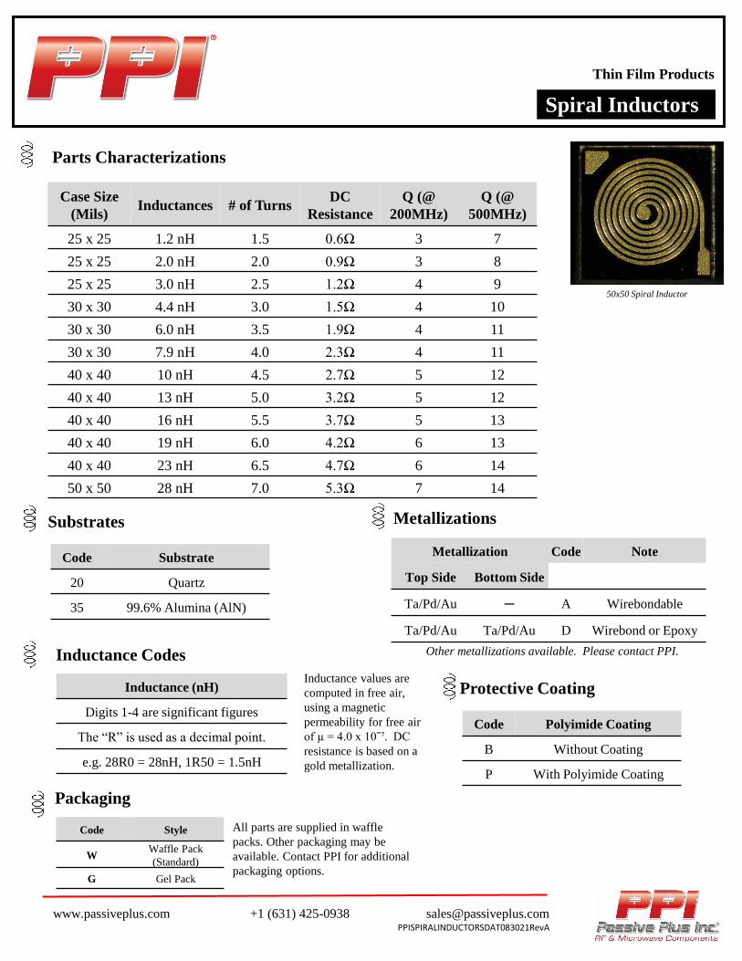
Parts Characterizations
Case Size
(Mils)Inductances # of Turns
DC
Resistance
Q (@
200MHz)
Q (@
500MHz)
25 x 25 1.2 nH 1.5 0.6Ω 3 7
25 x 25 2.0 nH 2.0 0.9Ω 3 8
25 x 25 3.0 nH 2.5 1.2Ω 4 9
30 x 30 4.4 nH 3.0 1.5Ω 4 10
30 x 30 6.0 nH 3.5 1.9Ω 4 11
30 x 30 7.9 nH 4.0 2.3Ω 4 11
40 x 40 10 nH 4.5 2.7Ω 5 12
40 x 40 13 nH 5.0 3.2Ω 5 12
40 x 40 16 nH 5.5 3.7Ω 5 13
40 x 40 19 nH 6.0 4.2Ω 6 13
40 x 40 23 nH 6.5 4.7Ω 6 14
50 x 50 28 nH 7.0 5.3Ω 7 14
Inductance values are
computed in free air,
using a magnetic
permeability for free air
of µ = 4.0 x 10ˉ⁷. DC
resistance is based on a
gold metallization.
50x50 Spiral Inductor
www.passiveplus.com +1 (631) 425-0938 [email protected]
Spiral Inductors
Thin Film Products
Inductance Codes
Inductance (nH)
Digits 1-4 are significant figures
The “R” is used as a decimal point.
e.g. 28R0 = 28nH, 1R50 = 1.5nH
Packaging
Code Style
WWaffle Pack
(Standard)
G Gel Pack
All parts are supplied in waffle
packs. Other packaging may be
available. Contact PPI for additional
packaging options.
Substrates
Code Substrate
20 Quartz
35 99.6% Alumina (AlN)
Metallizations
Metallization Code Note
Top Side Bottom Side
Ta/Pd/Au A Wirebondable
Ta/Pd/Au Ta/Pd/Au D Wirebond or Epoxy
Other metallizations available. Please contact PPI.
Protective Coating
Code Polyimide Coating
B Without Coating
P With Polyimide Coating
PPISPIRALINDUCTORSDAT083021RevA

General Properties
Operating Temperature -55°C to +150°C
Storage Temperature -65°C to +150°C
Operating Frequency DC to 500 MHz
Insulation Resistance 10¹²Ω ∙ min at 25°C
Testing Performed Specification / Standard
Visual InspectionMIL-PRF-55342
MIL-STD-883
Mechanical Inspection MIL-PRF-55342
DC ResistanceMIL-PRF-55342
MIL-STD-202
High Temperature Exposure MIL-PRF-55342
Thermal ShockMIL-PRF-55342
MIL-STD-202
Resistance to Bonding Exposure MIL-PRF-55342
Wire Bonding Integrity MIL-PRF-55342
Life TestMIL-PRF-55342
MIL-STD-202
Testing
Additional sizes and custom inductors available. Please contact [email protected].
Performance Specifications
50x50 Spiral Inductor
www.passiveplus.com +1 (631) 425-0938 [email protected]
Spiral Inductors
Thin Film Products
PPISPIRALINDUCTORSDAT083021RevA

Headquarters: New York, USA