thin films: processing & characterization application to...
TRANSCRIPT

1
Thin films: processing & characterization
Application to functional complex oxides
LMGP - UMR CNRS/INPG 5628INPG-Minatec 3 parvis L. Néel, BP25738016 [email protected]
Catherine DUBOURDIEUCNRS
OUTLINE
• Introduction• Thin films• Why do we need to control the growth at nanometer scale ?
•Thin films deposition methods
• Substrates: nature, preparation…
• Thin films characterizations
• Thin films of multiferroic compounds

2
Film (= layer)
Substrate
Thin films : t < 1 m
For microelectronic applications: usually t < 100 nm
T >> 1 m : coating
Amorphous
HfO2 on Si (001)
Epitaxial film
La0.7Sr0.3MnO3on SrTiO3 (001)Polycristalline film
SrTiO3on Si (001)
From Chem. Vap. Deposition 5 (1), 7 (1999)
Al203 300 nm on Si wafers with trench structures
TiN on patterned substrates
The substrate can be non-planar (in such a case, conformal coverage is required)

3
-Protective coating (diffusion barrier, corrosion protection…)
- Mechanical …
- Microelectronic applications
- Optics
…
Application of films
Complex oxides (electron correlated systems):
- High-Tc superconductors
- Ferroelectrics
- Magnetic, magnetoresistive
- Multiferroics…
Integrated circuits: oxides with high permittivity
LaMnO3 (AF/I)
La0.7Sr0.3MnO3 (FM/M)
ABO3
Dielectrics LaAlO3, SrTiO3 …Ferroelectrics BaTiO3, PbTiO3 …Pyroelectrics LiNbO3 …Ferromagnets SrRuO3, La0.7Sr0.3MnO3 …Conductors SrRuO3 , LaNiO3 …Magnetoresistive La0.7Sr0.3MnO3 …Semiconductors Nb-doped SrTiO3…Superconductors YBa2Cu3O7 , (La,Sr)2CuO4 ……
Complex oxides: large variety of physical properties
Crystalline structures:Perovskite or perovskite-relatedSpinelPyrochloreRock saltFluoriteLayered structures e.g. Ruddlessen-Popper…

4
Coupling between spin, orbital, charge and lattice (static and dynamics effects)
<---> Strong impact of an external excitation (H, E, h …) on these interactions
Great potential for applications - Memories (MRAM, Fe-RAM…) - CMOS - Sensors - Actuators - Catalysts …
Spin
Charge Orbital
Lattice
Fundamental physics - Understand coupling between order parameters - Determine characteristic lengths of the system (including domains size) - Understand size effects on the properties: when dimension(s) become(s) of the order of a
characteristic length, physical properties change
Complex oxides: (strongly) correlated electron systems
Materials (<--> properties) engineering using the large number of possible spin, orbital, chargeand lattice interactions (competing effects, cooperating effects…)
Thin films: Strain (lattice is strongly impacted by strain) Interface with substrate
Heterostructures: Multilayers,Nanostructured oxides
Strain Interfaces between oxides Proximity effects …
SubstrateSubstrate
Substrate
Spin
Charge Orbital
Lattice
Thin films: properties engineering
~10 Å
Need to control growth at unit-cell scale

5
SiGaAs
Ge
SiC
Semiconductors:
Engineering of properties (charge carrier, band gap…)
through doping, solid solution…
Oxides: Engineering of properties also possible !!
C.H. Ahn, J.M. T risone, J. Mannhart
Nature 424, 1015 (2003)
Silicon
drainsource
Dielectric
oxideGate electrode
(poly-Si or metal)
Spacer
MOS field-effect transistor (MOS-FET):
L
Pitch
Cox = 0 rox
tox
6
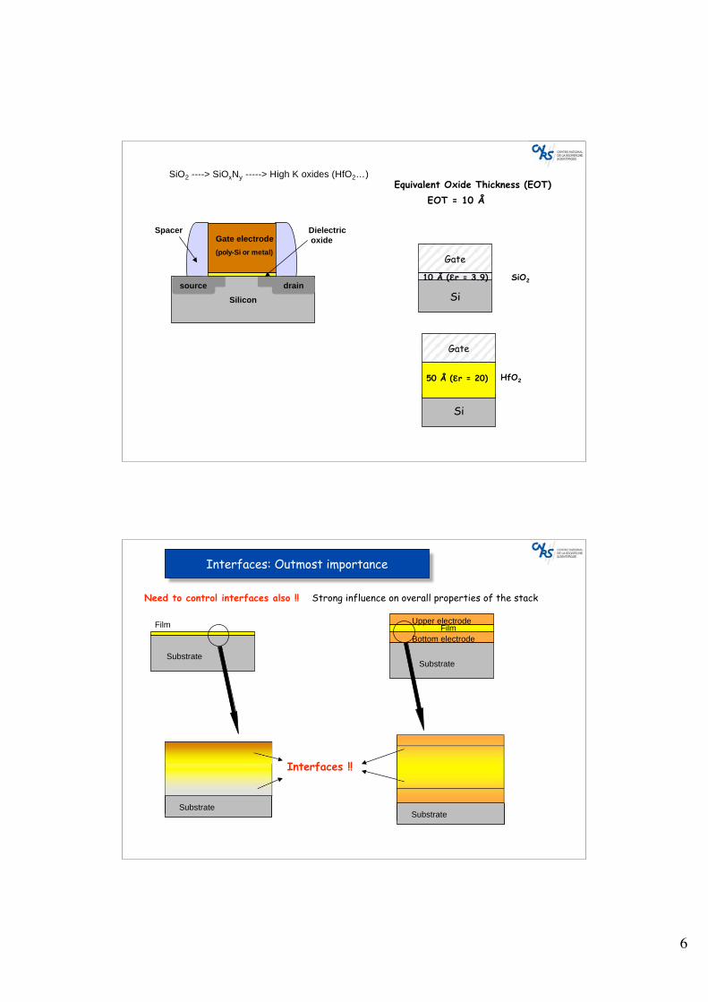
SiO2 ----> SiOxNy -----> High K oxides (HfO2…)
Silicon
drainsource
Dielectric
oxideGate electrode
(poly-Si or metal)
Spacer
Si
Gate
50 Å ( r = 20)
Equivalent Oxide Thickness (EOT)
EOT = 10 Å
Si
Gate
10 Å ( r = 3.9)
HfO2
SiO2
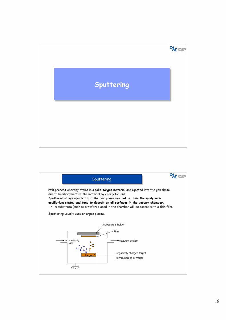
Substrate
Film
Interfaces !!
Substrate
Film
Substrate
Upper electrode
Bottom electrode
Substrate
Interfaces: Outmost importance
Need to control interfaces also !! Strong influence on overall properties of the stack

7
Si
Gate
50 Å ( r = 20)
Si
Gate
15 Å ( r = 20)7 Å ( r = 3.9)
HfO2HfO2SiO2
Equivalent Oxide Thickness (EOT)
EOT = 10 Å
Interfaces: Outmost importance
SiO2 (Silicate ? Silicide ?)
Silicon
drainsource
Gate electrode
Spacer
SiO2 ----> SiOxNy -----> High K
Lower interface:
- Chemical stability with Si
- Electrical compatibility
If HfO2 directly on Si : severe degradation of mobility
----> SiO2 (~ 5 Å) necessary
Interfacial defects have high impact on carrier mobility in channel
High K oxide
Silicon
Interfaces: Outmost importance

8
High K oxide
HfSixOy or HfO2
SiOxNY
Hf-Si-O-N
Silicon
drainsource
Gate
electrode
Spacer
Upper interface:
- Chemical stability with poly-Si or with metal ?
ZrO2 reacts with poly-Si
HfO2 stable with poly-Si
- Electrical compatibility ?
Poly-Si replaced by metal gate
Capping of metal in order to avoid oxygen diffusion
Tuning of metal work function with additives in high K or
with additional layer on top of high KMetal
Poly-Si
Poly-Si
Interfaces: Outmost importance
Interfaces: Outmost importance
Multilayers: succession of interfaces ---> Properties may arise from the interfaces
Herbert Kroemer, Nobel Price lecture 2000:
About semiconductors heterostructures: “…the interface is the device”
InP
InP
Alternance of
InGaAlAs/InP
QWs: InGaAlAs/InGaAs
SiGaAs
Ge
SiC

9
Oxides superlattices:
Field-effects
Recovery of ferroelectricity in (PbTiO3 / SrTiO3)n for ultrathin PbTiO3 layer: J.M. Triscone & M. Dawbers
…
C.H. Ahn, Science 284, 1153 (1999)
C.H. Ahn, J.M. T risone, J. Mannhart
Nature 424, 1015 (2003)
Substrate
Synthesis of thin films:main techniques
Physical Vapor Deposition (PVD) : MBE, laser ablation, sputtering
Chemical Vapor Deposition (CVD), Atomic Layer Deposition (ALD)

10
Molecular Beam Epitaxy (MBE)
Molecular Beam Deposition (MBD)
Epitaxy: “Above” (epi) and “in an ordered manner” (taxis)
In solid-source MBE, ultra-pure elements (such as gallium and arsenic) are heated in separate quasi-knudsen effusion cells until they begin to slowly evaporate. The evaporated elements then condense onthe wafer, where they may react with each other.Example: Ga and As ---> gallium arsenide single-crystal
The term "beam" means that evaporated atoms do not interact with each other or any other vacuumchamber gases until they reach the wafer, due to the long mean free paths of the beams.
Other variations include gas-source MBE, which resembles chemical vapor deposition.
MBE takes place in high vacuum or ultra high vacuum (10-11 Torr) ---> slow deposition rate---> requires stringent control of impurities
Computer controlled shutters in front of each furnace allow a precise control of the thickness of each layer.
Intricate structures of layers of different materials may be fabricated this way. Such control has allowedthe development of structures where the electrons can be confined in space, giving quantum wells or evenquantum dots. Such layers are now a critical part of many modern semiconductor devices, includingsemiconductor lasers and light-emitting diodes.
Molecular beam Epitaxy (MBE)Molecular beam Deposition (MBD)

11
Molecular beam epitaxy: developed in the 1960’s - need for making new crystalline materials for semi-conductors applications (concept of two layers with different semiconductors by H. Kroemer in the 50’s) .
Mostly at IBM (in Yorktown Heights, NY) and Bell Laboratories (in Murray Hill, NJ), 1968-1973
John R. Arthur Jr. and Alfred Y. Cho
A. Cho honoured with US National Medal of Technology (announced June 14th 2007 by Alcatel-Lucent)
Leo Esaki and Ray Tsu at IBM: concept known as superlattice (“a valuable area of investigation in the field of semiconductors”)
“MBE deserves a place in the history books”, by W. Patrick MCCRAY, Nature Nanotechnology May 2007, p.259
MBE played a central role in the growth and development of nanoscience and nanotechnology
Molecular beam Epitaxy (MBE)
InP
InP
Alternance ofInGaAlAs/InP
Molecular beam Epitaxy (MBE)

12
Molecular beam Epitaxy (MBE)
Introduction chamber
CryopumpValve
Transfer chamber
Ionic Pump
Growth chamber

13
Ga
AlMn
N
SiGrowth chamber
Introduction chamberTransfer chamber
Sapphire substrate
20 cm GaNMixing zone
Molecular beam Epitaxy (MBE)
RHEED (Reflection High Energy Electron Diffraction) is often used for in situ monitoring the growth
RHEED monitoring during Molecular beam Epitaxy (MBE)

14
RHEED monitoring during Molecular beam Epitaxy (MBE)
Applications to oxides:
Need oxygen source for growing oxides: atomic oxygen usually used (differential pumping system)
Atomic sources (effusion cells) or ceramic which are evaporated using electron-beam guns
Quite widely used for high-K oxides research (G. Hollinger at INL-Lyon, J. Fompeyrine IBM Zürich, T.Schroeder IHP Germany, Osten Germany, G. Norga Italy, M. Fanciulli Italy, D. Schlom USA…)
Complex oxides films and heterostructures:
J.P. Locquet at IBM ZürichD. Schlom USA…
Molecular beam Epitaxy (MBE)

15
Pulsed Laser Deposition (PLD)
Pulsed laser deposition works by an ablation process ( PVD technique) .High power pulsed laser beam is focused inside a vacuum chamber to strike a target of thedesired composition. Material is then vaporized from the target and deposited as a thin filmon a substrate facing the target.
This process can occur in ultra high vacuum or in the presence of a background gas, such asoxygen which is commonly used when depositing oxides to fully oxygenate the depositedfilms.
Pulsed laser deposition

16
While the basic-setup is simple relative to many other deposition techniques, the physicalphenomena of laser-target interaction and film growth are quite complex.
When the laser pulse is absorbed by the target, energy is first converted to electronicexcitation and then into thermal, chemical and mechanical energy resulting in evaporation,ablation, plasma formation... The ejected species expand into the surrounding vacuum in theform of a plume containing many energetic species including atoms, molecules, electrons,ions, clusters, particulates and molten globules, before depositing on the typically hotsubstrate.
A plume ejected from a SrRuO3 target duringpulsed laser deposition
Pulsed laser deposition
1960: T.H. Maiman constructed the first optical maser using a rod of ruby as the lasing medium
1962: Breech and Cross used ruby laser to vaporize and excite atoms from a solid surface
1965: Smith and Turner used a ruby laser to deposit thin films -> very beginning of PLD technique development
However, the deposited films were still inferior to those obtained by other techniques such aschemical vapor deposition and molecular beam epitaxy.
Early 1980’s: a few research groups (mainly in the former USSR) achieved remarkable resultson manufacturing of thin film structures utilizing laser technology.
1987: Dijkkamp and Venkatesan prepared thin films of YBa2Cu3O7 by PLD
In the 1990’s: development of new laser technology, such as lasers with high repetition rateand short pulse durations, made PLD a very competitive tool for the growth of thinfilms withcomplex stoichiometry.
Pulsed laser deposition
http://pulsedlaser.net

17
Pulsed laser deposition
Applications to oxides:
Need oxygen source for growing oxides: not in ultrahigh vacuumCeramic target(s) needed - several targets can be usedExcimer laser ( = 248 nm)RHEED: need differential pumping system because of “elevated” background pressure due to oxygen
Widely used in laboratories (transfer of the target composition to the film composition, control ofdeposited thickness, more simple than MBE to set up)
Drawback: generate particles
18
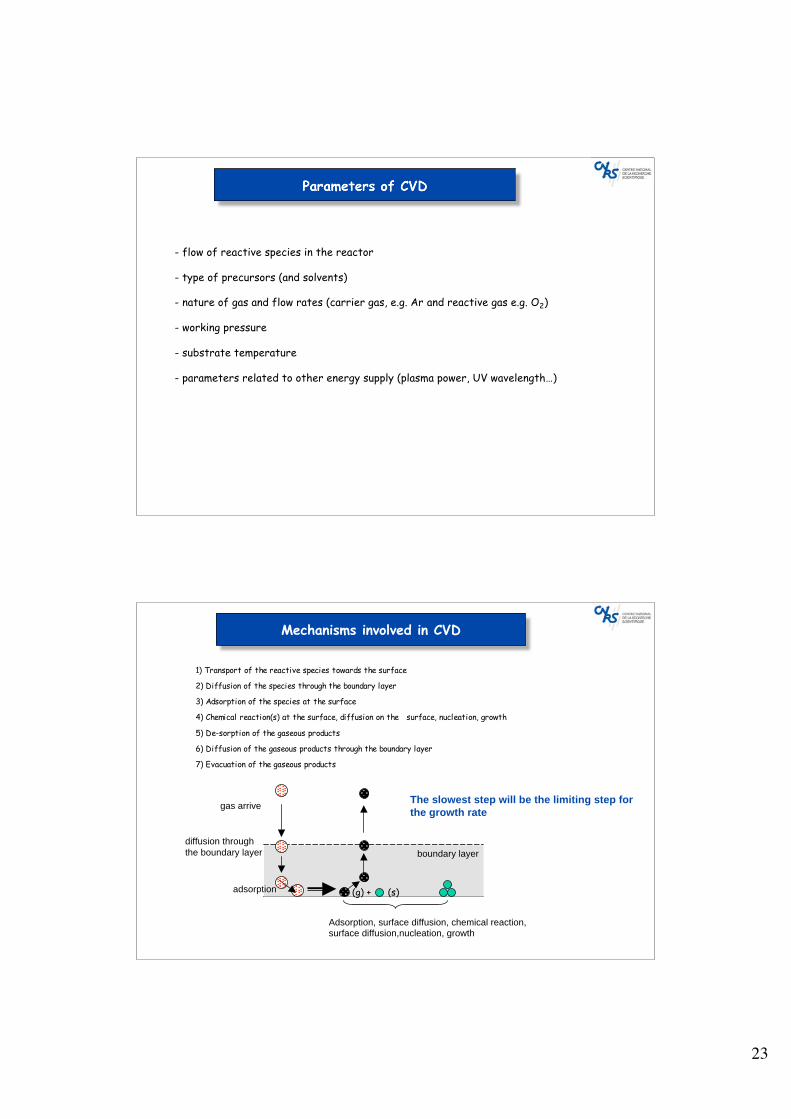
Sputtering
PVD process whereby atoms in a solid target material are ejected into the gas phasedue to bombardment of the material by energetic ions.Sputtered atoms ejected into the gas phase are not in their thermodynamicequilibrium state, and tend to deposit on all surfaces in the vacuum chamber.--> A substrate (such as a wafer) placed in the chamber will be coated with a thin film.
Sputtering usually uses an argon plasma.
Target
Substrate’s holder
Film
Ar sputtering
gas Vacuum system
Negatively charged target
(few hundreds of Volts)
Ar+
Sputtering

19
Standard physical sputtering is driven by momentum exchange between the ions andatoms in the material, due to collisions (Behrisch 1981, Sigmund 1987).
Analogy with atomic billiards: the ion (cue ball) strikes a large cluster of close-packedatoms (billiard balls).
Energy of impinging ions: < 10 eV: elastic backscatting of the ions
10 à 1000 eV: sputtering of the target
> 1000eV: ions implantation
The number of atoms ejected from the surface per incident particle is called the sputteryield and is an important measure of the efficiency of the sputtering process.
Sputter yield depends on: - the energy of the incident ions (>> 10 eV) , which depends ontarget gun’s bias voltageAr gas pressure
- the masses of the ions and of target atoms- the binding energy of atoms in the solid
Sputtering
Various techniques are used to modify the plasma properties (especially its iondensity) in order to optimize the sputtering conditions:
Negative bias of the target
RF sputtering: alternating current for biasing insulating target
Magnetron: confinement of the plasma in the vicinity of the target
off-axis target: avoid sputtering of the film
Sputtering

20
Reactive sputtering: a reactive gas is added to the usual Ar sputtering plasma to shiftcompound-film stoichiometry in sputtering from a compound target or to deposit acompound from a metallic target.
1) Arise from a tendency for the electronegative elements to become depleted incompound sputtering. Although both elements must leave the surface at the targetcomposition ratio in steady state, the sticking coefficient of the electronegativeelement at the substrate is likely to be lower resulting in a sub-stoechiometric deposit
-- > addition of an appropriate amount of that element to the supply flow of sputtering gas
2) A small amount of oxygen or nitrogen is mixed with the plasma-forming gas. After thematerial is sputtered from the target, it reacts with this gas, so that the deposited filmis a different material, i.e. an oxide or nitride of the target material.
Ex : Ti target + nitrogen : TiN formation
Sputtering
Sputtering
Applications to oxides:
Ceramic target(s) or metallic target + oxygen - several targets can be used (shutters)
Widely used in laboratories (transfer of the target composition to the film composition however notsystematic)

21
Chemical Vapor Deposition
Chemical routes: Classification
Substrate
Condensation of the
precursor
(lquid or solid)
Nothing
ALD CVD
Adsorption
IncorporationReaction in
heterogeneous
phase
Reaction in
homogeneous phase
T Tevap.T < Tevap.powder
Gazeous phase
Solid precursorSolid precursor in a solvant
Liquid precursor
Liquid phase Liquid phase
aerosol/spray
Pyrosol MOD Sol gel(atm pressure) (atm. pressure)
dip coating
spin coating
aerosol
Evaporationsublimators
bubblers
injection into an evaporator
aerosol in an evaporator
...
CVD

22
Gas A ------> Solid B + Gas C
kT (hw…)
Heterogeneous phase reaction(s) (gas/surface)
Deposition of a solid film on a heated surface via chemical reaction(s)
Source systemGeneration of the
gas phase
Transport of the gas and distribution
exhaustReaction zone
Chemical vapor deposition (CVD)
Chemical vapor deposition (CVD)
Different issues with CVD:
Type of source : how can I generate the gas phase ? (it depends on the precursors)
How to promote the reactions : - thermal (resistive, inductive, radiative (IR) heating)- plasma (PE-CVD)- UV- laser
Working pressure : atmospheric pressure (APCVD) or low pressure (LPCVD)
Design of the reactor (vertical, horizontal, cold or hot walls, orientation of the substraterelatively to the gas flow, optical ports for in situ characterization….)
23
Parameters of CVD
- flow of reactive species in the reactor
- type of precursors (and solvents)
- nature of gas and flow rates (carrier gas, e.g. Ar and reactive gas e.g. O2)
- working pressure
- substrate temperature
- parameters related to other energy supply (plasma power, UV wavelength…)
Mechanisms involved in CVD
1) Transport of the reactive species towards the surface
2) Diffusion of the species through the boundary layer
3) Adsorption of the species at the surface
4) Chemical reaction(s) at the surface, diffusion on the surface, nucleation, growth
5) De-sorption of the gaseous products
6) Diffusion of the gaseous products through the boundary layer
7) Evacuation of the gaseous products
(g) + (s)
Adsorption, surface diffusion, chemical reaction, surface diffusion,nucleation, growth
gas arrive
diffusion through
the boundary layer
adsorption
boundary layer
The slowest step will be the limiting step for
the growth rate

24
Mechanisms of the CVD process
Log (growth rate)
1/T
Kinetic
Diffusion
Reactions in homogeneous phase
Growth controlled by surface : the growth rate is limited by the kinetic of the chemical reactions
---> highly dependent on surface temperature
Growth controlled by diffusion : the growth rate is limited by the income of the reactive species at the surface
(diffusion in the boundary layer) ---- > not very dependent on surface temperature
Chemical reactions used in CVD
Thermal decomposition : AB(g) ----> A(s) + B(g) SiH4(g) ----> Si(s) + 2 H2(g)
(pyrolysis) Al(OC3H7)3 ----> Al2O3 + CxHy + H2O
Al(C4H9)3 ----> Al + 3 C4H8+ 3/2 H2
Reduction : 2 AX(g) + H2(g) ----->2A(s) + 2 HX(g) SiCl4(g) + 2 H2(g) ----> Si(s) + 4 HCl(g)
WF6(g) + 2 H2(g) ----> W(s) + 6 HF(g) 3 NbCl5(g) + GeCl4(g) + 19/2 H2(g) ----> Nb3Ge(s) +19 HCl(g)
Oxydation : 2 AX(g) + O2(g) ----> 2AO(s) + X2(g) SiH4(g) + O2(g) ----> SiO2(s) + 2 H2(g) SiH4(g) + 2 O2(g) ----> SiO2(s) + 2 H2O(g) Zn(C2H5)2 + 7 O2(g) ----> ZnO(s) + 4 CO2+ 5H2O(g)
Polymerisation : n AB ----> (AB)n Si2(CH3)6O ----> _(Si(CH3)2O)n_
Any chemical reaction which imply one or several gaseous reactive species and that can lead tothe desired solid (with gaseous by-products)

25
Hydrolysis : AX(g) + H2O(g) ----> AO(s) + HX(g) SiCl4(g) + 2H2O (g) ----> SiO2(s) + 4 HCl(g) (CO2 + H2)
Nitridation : AX(g) + NH3(g) ----> AN(s) + HX(g) 3 SiCl4(g) + 4 NH3(g) ----> Si3N4(s) + 12 HCl(g)GaCl + NH3(g) ----> GaN + H2(g)+ HCl(g)
Carburation : AX4(g) + CH4(g) ----> AC(s) +4 HX(g) SiCl4 (g )+ CCl4 (g )+4H2 (g) ----> SiC(s) + 8HCl(g)
Reactions of synthesis between two (or more) volatile compounds
hydride + halide, OM + hydride, OM+OM... Ga(CH3)3(g) + AsH3 ----> GaAs (s) + 3 CH4(g) Cd(CH3)2 + H2Se(g) ----> CdSe (s) + 2 CH4(g)
Combined reactions ...
Chemical reactions used in CVD
Crucial point for the CVD process
Precursors :
Gas ex. : SiH4(g) -------> Si(s) + 2 H2(g)
Liquid need to be evaporated
Solid need to be evaporatedHow to perform the evaporation ??
Objective: stable gas phase
Gas phase generation

26
Gas phase generation: classical ways
Solid precursor
The gas phase is controlled by: - source temperature - pressure - carrier gas flow rate - amount of precursor (surface)
Alumina boat
Evaporation rate vs T° for Y(tmhd)3, Ba(tmhd)2 and Cu(tmhd)2
The evaporation rate depends strongly on theevaporation temperature
Precursor powder
Gas phase generation: classical ways
Liquid precursor: Bubblers
The gas phase is controlled by: - bubbler temperature - bubbler pressure - carrier gas flow rate - amount of liquid
MFCAr
Bubbler heater Liquid precursor
Ar + precursor vapor

27
Precursors requirements
- Volatility as high as possible (minimizing of evaporation temperature) with high vapor
pressure (for reasonable growth rate)
- Adequate temperature window between evaporation and decomposition (thus Tvap < 300°C)
- Thermal stability (no decomposition during heating)
- By-products of the reactions must be gaseous
- Toxicity, environmental and safety issues, handling, storage (shelf life), price...
With classical sources, it is difficult to:
- control the vapor flow at low pressure
- obtain a high vapor pressure
- use thermally unstable precursors
Example : superconducting oxide YBa2Cu3O7 (first results with CVD in 1988)
Precursor for Y, Ba, Cu ?
Halides : evaporation temperature too high (> 800°C)
Organometallic molecules: lower evaporation temperature (< 250°C)
-diketonates
M(2,2,6,6 tetramethyl 3,5 heptane dionate)n = M(tmhd) n
Gas phase generation:organometallic precursors for oxide deposition
tmhd ligand

28
Y
H
C(CH3)3
OO
C
CC(H3C)3C
H C(CH3)3
O
O
C
C
C
(H3C)3CO
OC
C C
C(CH3)3
C
(CH3)3
H
Y
H
C(CH3)3
OO
C
CC
OO
C
CC(H3C)3C
H C(CH3)3
O
O
C
C
C
(H3C)3CO
OC
C C
C(CH3)3
C
(CH3)3
H
Y(tmhd)3
- Bad thermal stability
- Sensitivity to humidity
- Evaporation temperature close to the decomposition temperature
Drift of the vapor pressure during deposition !!!
QUESTION
How to generate a stable gas phase from unstable precursors ?
- Maintain precursors at room temperature
- Evaporate micro-quantities of precursors in a “flash” manner
Innovative sources for the generation of the gas phase
Some precursors (especially for Ba, Sr, Ca and Rare-earth) exhibit:

29
Ar
“flash” evaporation of the precursors
Solid sources (solid precursor) :
- solid stick introduced in a sharp thermal gradient
Innovative sources
Liquid sources (liquid precursor ou solid precursor dissolved in a solvent)
- delivery of the liquid in an evaporator via - a micro-pump- a syringe- a liquid mass flow
- an injector
- a aerosol
drawback : mixing of powders difficult to control
Alternative source : injection source (LMGP-CNRS)
Micro-valve
Glass container
Pressurisation under Ar
Injection of micro-quantities of liquid in an evaporator (T ~ 250°C)
- “flash” evaporation
- liquid precursor maintained at room temperature
CNRS (LMGP) 1993 - 1994 patents - licenced by CNRS to AIXTRON(France, Europe, USA)
30
substrate
4.0
4.5
5.0
5.5
6.0
0 500 1000 1500 2000
Pre
ssio
n
(Torr
)
Temps
Début de l'injection
régime transitoire
Injection : pulsed regime (pressure oscillations)
Alternative source : injection source (LMGP-CNRS)
Control of the gas phase in injection-CVD
REACTIVES SPECIES FLOW RATE IN GAS PHASE CONTROLLED BY:
- injection frequency (~ 0.1 to few Hz)
- opening time (~ 1 ms / 10 ms)
- dilution of precursors solution
- solvent (viscosity)
- differential pressure between liquid contained and evaporator
remember : for classical source this control is performed through : evaporation temperaturepressurecarrier gas flow

31
Advantages of this injection delivery scheme
- Thermally unstable precursors can be used (precursors maintained at room T°. under an inert gas / flash volatilisation)
- Deposition of complex oxides : unique liquid solution can be used (mixture in a single cocktail of several precursors)
stability of the gas phase composition
- Large growth rate range possible
- No dead volume : growth stops as injection is stopped
- Sequential use of several injectors
growth of heterostructures, multilayers

32
Alternative source : injection source - other examples
Liquid injection system based on mass-flow controllersH.J. Boer, Solid State Technology, March 1996, p. 149
out
Evaporator
Liquid flow valve
Liquid flow meterMFC
Gas
Gas/liquidmix
Bronkhorst system
Continuous injection of liquid into the evaporator
Modelling of CVD
Need to simultaneously model both the complex chemistry and the complex fluid flow
Chemistry:Need to know the reactions pathways and the kinetic constant of the different reactions
---> difficult to identify all the reactions (for a simple case os Si, the number ofsimultaneous homogenous and heterogeneous reactions is of a few tens)
kinetic of the reactions: for homogenous reaction : Arrhenius-type lawfor heterogenesous reaction: more difficult to determine and model
Unimolecular reaction (dissociation, isomerisation)
Bi-molecular reaction CH4 + .H <--> .CH3 + H2
.H + CH3C6H5 <--> C6H6 + .CH3
.H + C2H4 <--> .C2H5
See papers from M. Pons, M. Allendorf, and also Sandia laboratory
33
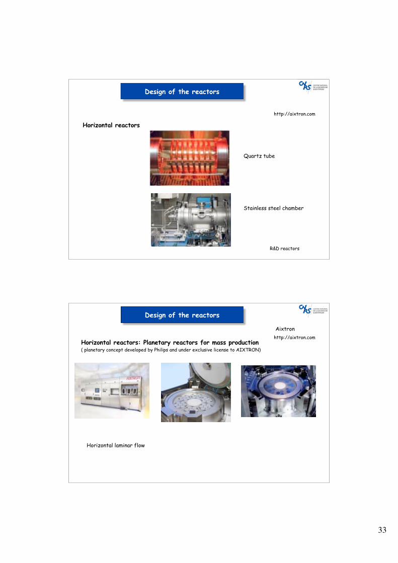
Design of the reactors
http://aixtron.com
Horizontal reactors
R&D reactors
Quartz tube
Stainless steel chamber
Design of the reactors
http://aixtron.comHorizontal reactors: Planetary reactors for mass production( planetary concept developed by Philips and under exclusive license to AIXTRON)
Horizontal laminar flow
Aixtron

34
http://www.thomasswan.co.uk/
Thomas Swan
Design of the reactors
Vertical reactors
A showerhead is used for the precursor gas distribution
200-300 mm MOCVD equipment for oxide deposition
ST / LETI-CEA
35
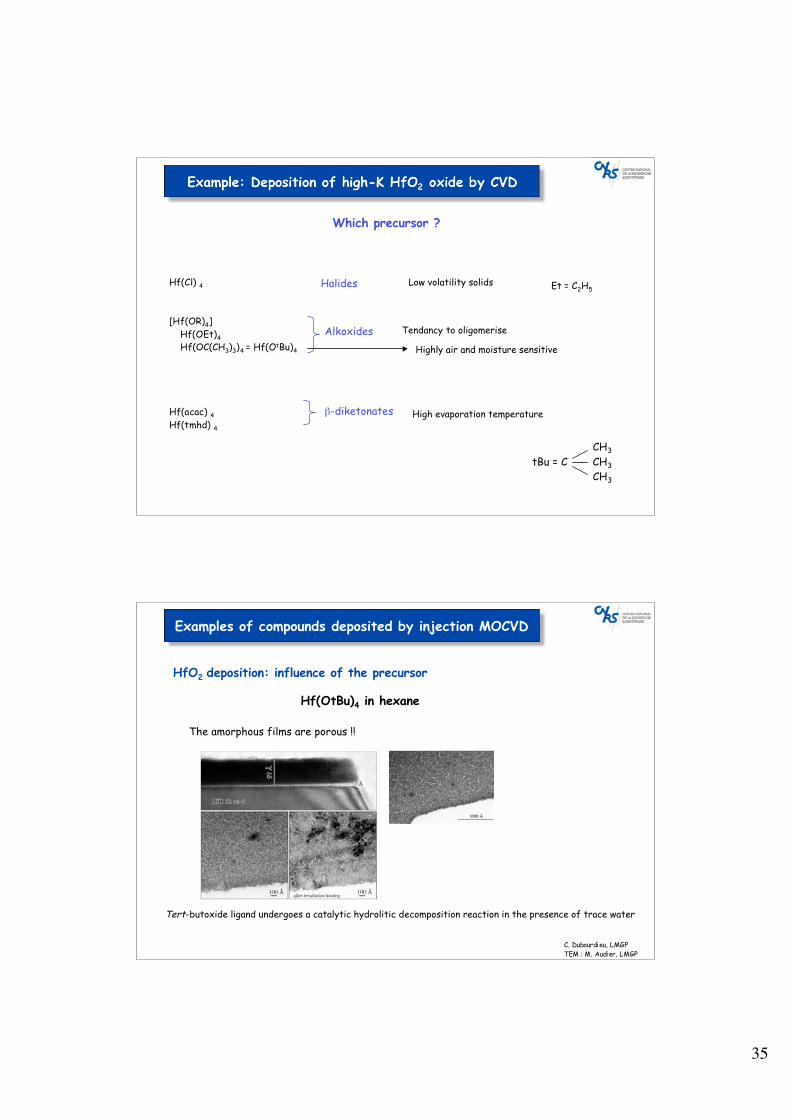
Example: Deposition of high-K HfO2 oxide by CVD
Which precursor ?
Hf(Cl) 4
[Hf(OR)4] Hf(OEt)4
Hf(OC(CH3)3)4 = Hf(OtBu)4
Hf(acac) 4Hf(tmhd) 4
CH3
tBu = C CH3
CH3
Alkoxides
-diketonates
Halides Low volatility solids
Tendancy to oligomerise
Highly air and moisture sensitive
Et = C2H5
High evaporation temperature
Examples of compounds deposited by injection MOCVD
HfO2 deposition: influence of the precursor
Hf(OtBu)4 in hexane
The amorphous films are porous !!
Tert-butoxide ligand undergoes a catalytic hydrolitic decomposition reaction in the presence of trace water
C. Dubourdieu, LMGPTEM : M. Audier, LMGP

36
Example: Deposition of high-K HfO2 oxide by CVD
C. Dubourdieu, LMGPTEM : G. Van Tendeloo, EMAT, Anvers
Which precursor ?
Hf(NMe2)4 : high sensitivity to moisture Mp = ~75oC
Hf(NEt2)4 : high sensitivity to moisture Mp = ~42oC
Hf(OtBu)2(dmae)2 : low sensitivity to moisture Mp = ~75oC
Hf(OtBu)2(mmp)2 : low sensitivity to moisture Mp = ~75oC
CH3
NMe2 = N CH3
CH2CH3
NEt2 = N CH2CH3
dmae = OCH2CH2N
CH3
CH3mmp = OC CH2OCH3
CH3
CH3
Amides
Alkoxide + dmae or mmp
Highly reactive in air
Example: Deposition of HfO2 by CVD
Precursor : Hf(OtBu)2(mmp)2
Solvent: Octane
Temperature: 350°CTotal pressure: 0.13 kPaAr + O2 (PO2 = 0.09 kPa)
C. Dubourdieu, LMGPTEM : G. Van Tendeloo, EMAT, Anvers
Ts = 350°C
Control of the thickness via theinjected volume of precursor
0
20
40
60
80
100
0.00 0.20 0.40 0.60 0.80 1.00 1.20 1.40
350°C
500°C
Th
ickn
ess
(Å)
V injected (ml)
178 Å/ml
55 Å/ml
0.2 nm/s
0.7 nm/s

37
Deposition of HfO2: effect of the reactive species flow rate
Decrease of the reactive speciesflow impinging on the substrate
Decrease of the interfacial layer thickness
C. Dubourdieu, LMGPTEM : G. Van Tendeloo, EMAT, Anvers
Example: Deposition of HfO2 by CVD
Epitaxial films of complex oxides
La0.7Sr0.3MnO3on SrTiO3 (001)
Example: Deposition of CMR manganites
-diketonates
Evaporation Temp. 250°C
Ts = 700°C
P = 5 Torr (Ar + O2)
PO2 = 1/3 Ptot
C. Dubourdieu, LMGP
G. Van Tendeloo, EMAT, Anvers
38
C. Dubourdieu, LMGP
TEM: G. Van Tendeloo (EMAT, Anvers)
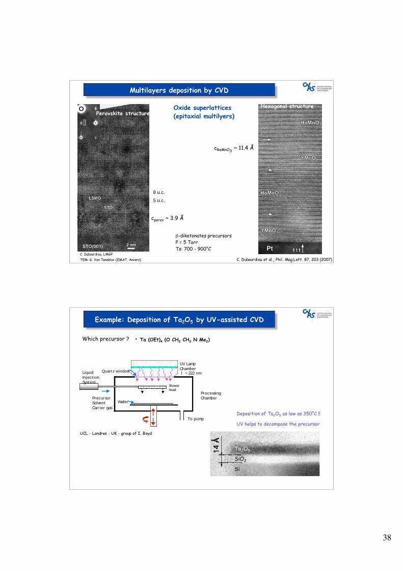
Multilayers deposition by CVD
Oxide superlattices(epitaxial multilyers)
cReMnO3 ~ 11.4 Å
Perovskite structure
cperov ~ 3.9 Å
Hexagonal structure
-diketonates precursorsP = 5 TorrTs: 700 - 900°C
5 u.c.
8 u.c.
C. Dubourdieu et al., Phil. Mag.Lett. 87, 203 (2007)
Example: Deposition of Ta2O5 by UV-assisted CVD
• Ta (OEt)4 (O CH2 CH2 N Me2)Which precursor ?
UV Lamp
Chamber
Processing
Chamber
To pump
l = 222 nm
Shower
head
Liquid
Injection
System
Precursor
Solvent
Carrier gas
Quartz window
Wafer
UCL - Londres - UK - group of I. Boyd
Si
SiO2
Ta2O5
Deposition of Ta2O5 as low as 350°C !!
UV helps to decompose the precursor
39
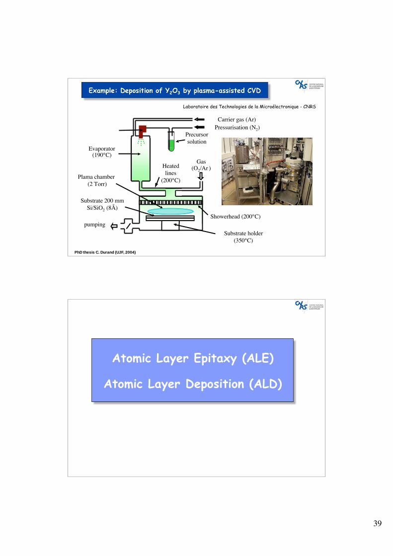
Laboratoire des Technologies de la Microélectronique - CNRS
Substrate 200 mmSi/SiO2 (8Å)
Plama chamber (2 Torr)
Substrate holder(350°C)
Showerhead (200°C)pumping
Heatedlines
(200°C)
Pressurisation (N2) Carrier gas (Ar)
Evaporator(190°C)
Gas(O2/Ar )
Precursorsolution
PhD thesis C. Durand (UJF, 2004)
Example: Deposition of Y2O3 by plasma-assisted CVD
Atomic Layer Epitaxy (ALE)
Atomic Layer Deposition (ALD)

40
Atomic Layer Deposition (ALD) or Atomic Layer Epitaxy (ALE)
T. Suntola, J. Antson, A. Pakkala and S. Lindfors, SID 1980 Digest (1980) 108
Extracted from : Nanostructures at Atomic Layer AccuracyReprint from : High Technology in Finland, 1997
Sequential exposure of the substrate surface to different precursors
In-between pulses of precursors: purge of the reactor with an inert gaz
Cycle de croissance : - pulse of precursor A- purge- pulse of precursor B- purge
Ideally: growth is self-limited by saturation of the surface(self-limited by adsorption à la surface)
the thickness of the film is directly proportional to the number of cycles
Advantages:Simple and precise control (in principle) of the thickness of the filmsUniformity over large surfacesConformal coverage over very large aspect ratio (1:50)Low temperature depositionNanolaminates (multilayers) deposition
Limitations (or particularities):Low growth rates (100-300 nm/h)
BUT : high productivity since simultaneous depostiion on a large number of wafers is possible (of large area)ex : 82 glass substrates of 155x265 mm2 simultaneously covered in a ALD reactor at Planar International for electroluminescent displays
Main applications: Electroluminescent displays
Solar cells
Microelectronic : synthesis of high K dielectrics, diffusion barriers and electrodes)
commercially used in the fabrication of magnetic read-heads (for insulating layers, mainly Al2O3) as well as for flat panels
Atomic Layer Deposition (ALD)

41
Compounds synthesized by ALD
Oxides
Dielectrics : TiO2, Ta2O5, ZrO2, HfO2, Al2O3, Nb2O5, SrTiO3, BaTiO3, Y2O3, MgO, CeO2
nano-laminates ex : Ta2O5,/HfO2
Transparent conducting / In2O3, In2O3:Sn (ITO), In2O3:F, In2O3:Zr, SnO2, SnO2:Sb, ZnO, ZnO:Al, Ga2O3
Semiconductors
Superconductors YBa2Cu3O7
Fluorides CaF2, SrF2, ZnF2
Nitrides NbN, TiN, TaN, MoN, AlN, GaN, InN, SiNx
III-V compounds GaAs, AlAs, InP, GaP, InAs, AlxGa1-xAs, GaxIn1-xAs,GaxIn1-xP
II-VI compounds ZnS, ZnSe, ZnTe, ZnS1-xSex, CaS, SrS, BaS, CdS, CdTe, MnTe, HgTe,
Hg1-xCdxTe,Cd1-xMnxTe
ZnS:M (M = Mn, Tb, Tm), CaS:M (M = Eu, Ce, Tb, Pb), SrS:M (M = Ce, Pb, Tb)
Elements Si, Ge, Cu
Others : La2S3, PbS, In2S3, CuGaS2, SiC
M. Ritala, Applied Surface Science 112, 223-230 (1997)
From Infineon (web source)
Atomic Layer Deposition (ALD): examples of realisationconformal coverage - aspect ratio 1:60 !

42
From Infineon (web source)
Atomic Layer Deposition (ALD): examples of realisationnanolaminates + conformal coverage
Example: growth of Ta2O5 by ALD
Cycle : pulse of Ta(OC2H5)5 - carrier gas N2
purge N2
pulse of H2O
purge N2
Effect of the pulse time of H2Oon the growth rate
Effet of the substrate temperatureon the growth rate Thickness / number of cycles
K. Kukli, M. Ritala, M. Leskelä, Journal of the Electrochemical Society 142 (5), 1670 (1995)
precursor supplied aloneCVD
43
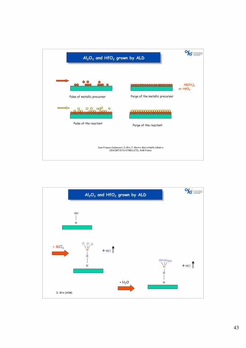
Al2O3 and HfO2 grown by ALD
Jean-François Dalencourt, D. Blin, F. Martin, Marie-Noëlle Séméria(CEA/DRT/DTS/STME/L2TI), ASM France
Pulse of metallic precursor Purge of the metallic precursor
Al(CH3)3or HfCl4
Pulse of the reactant Purge of the reactant
Si
OH
Si
O
M
Cl Cl Cl
+ HCl+ MCl4
Si
O
M
OH OHOH
+ HCl
+ H2O
D. Blin (ASM)
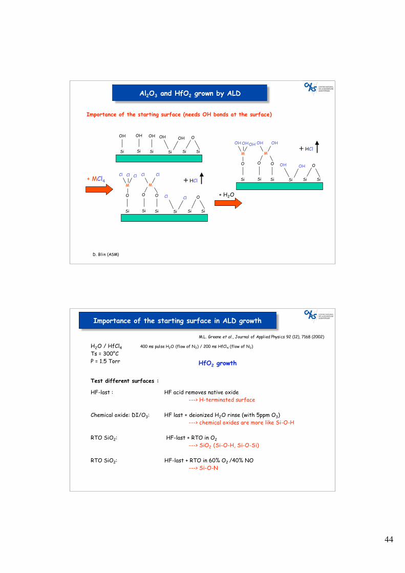
Al2O3 and HfO2 grown by ALD
44
Si
OH
Si
OH
Si
OH
Si
OHOH
Si
O
Si
Si
O
Si
O
Si
O
Si
ClCl
Si
O
Si
M
Cl Cl Cl
M
Cl Cl+ HCl+ MCl4 Si
O
Si
O
Si
O
Si
OHOH
Si
O
Si
M
OH OHOH
M
OH OH+ HCl
+ H2O
D. Blin (ASM)
Al2O3 and HfO2 grown by ALD
Importance of the starting surface (needs OH bonds at the surface)
Importance of the starting surface in ALD growth
M.L. Greene et al., Journal of Applied Physics 92 (12), 7168 (2002)
H2O / HfCl4 400 ms pulse H2O (flow of N2) / 200 ms HfCl4 (flow of N2)
Ts = 300°CP = 1.5 Torr
Test different surfaces :
HF-last : HF acid removes native oxide ---> H-terminated surface
Chemical oxide: DI/O3: HF last + deionized H2O rinse (with 5ppm O3)---> chemical oxides are more like Si-O-H
RTO SiO2: HF-last + RTO in O2
---> SiO2 (Si-O-H, Si-O-Si)
RTO SiO2: HF-last + RTO in 60% O2 /40% NO---> Si-O-N
HfO2 growth

45
M.L. Greene et al., Journal of Applied Physics 92 (12), 7168 (2002)
Importance of the starting surface in ALD growth
HfO2 growth on different starting surfaces : HF-last, chemical SiO2 oxide, RTOSiO2 , RTNO Si-O-N...
Importance of the starting surface in ALD growth
Slope of linear regression fit to the chemical oxide data:
1.26 ±0.01 x 10¹⁴ Hf/cm2/cycle
Maximum HfO2 coverage per ALD cycle : 9.15x10¹⁴ HfO2/cm2
Only 14% coverage is achieved per cycle
Steric hindrance or lack of reactive sites result in only partial monolayer growth per cycle

46
C. F. Hermann et al., APL 87, 123110 (2005)
ALD and nanomaterials
Coating of carbon nanotubes
Substrate:Nature, orientation, preparation, surface
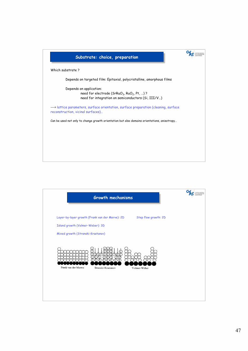
47
Which substrate ?
Depends on targeted film: Epitaxial, polycristalline, amorphous films
Depends on application:need for electrode (SrRuO3, RuO2, Pt, …) ?need for integration on semiconductors (Si, III/V…)
---> lattice parameters, surface orientation, surface preparation (cleaning, surfacereconstruction, vicinal surfaces)…
Can be used not only to change growth orientation but also domains orientations, anisotropy…
Substrate: choice, preparation
Growth mechanisms
Layer-by-layer growth (Frank van der Merve): 2D Step flow growth: 2D
Island growth (Volmer-Weber): 3D
Mixed growth (Stranski-Krastanov)

48
Films growth
Growth of crystalline surfaces at atomic scale :
(W. Kossel, Nachr. Ges. Göttingen, math-phys. Klasse, (1927) 135)
TLK (ou TSK) model : Terrace-Ledge-Kink (or Terrace-Step-Kink)
Terrasse - Lisière (marche) - Cran
t < tcrit
Buffer layer(can have graded composition)
Dislocations
Epitaxy: Growth of a single crystal (A) on a single crystalline substrate (B)
A=B homoepitaxyA B heteroepitaxy
- Choose substrate of same crystalline structure (e.g. perovskite) and with small latticemismatch (aA-aB)/aB
- If mismatch too large: use sacrificial buffer layer where relaxation will takes place withdislocations formation
- Case of epitaxial phase stabilization
A
B
Both film and substrate are strained

49
RMnO3 : “perovskite structure” (Pnma) RMnO3 : hexagonal structure
Ce Pr Nd Pm Sm Eu Gd Tb Dy Ho Er Tm Yb Lu
La Y
As thin films: find appropriate substrate <---> epitaxial stabilization
As bulk : stabilization of hexagonalDyMnO3 (synthesis at 1600°C andquenching )No other case reported to our knowledge
1/2R2O3 + 1/2Mn2O3 <---> RMnO3
-70
-60
-50
-40
-30
1.05 1.10 1.15 1.20
Gf (R
Mn
O3)
kJ/
mo
l
r ionique
(Å)
LuHo
Dy
La
GdEu
Sm
he
xa
go
na
le
ph
as
e
perovskite phase
T. Atsumi et al., J. Alloys and Compounds 238, 35 (1996)
Epitaxial phase stabilisation
RMnO3 : “perovskite structure” (Pnma) RMnO3 : hexagonal structure
Ce Pr Nd Pm Sm Eu Gd Tb Dy Ho Er Tm Yb Lu
La Y
Choice of substrate of high importance <---> epitaxial stabilisation
YSZ (111)Pt (111)Si (111)
YMnO3 hexagonalYMnO3 hexagonal
Substrate of perovskite structure(SrTiO3, LaAlO3)
YMnO3 perovskiteEpitaxial stabilisation
Epitaxial phase stabilisation for cubic YMnO3

50
RMnO3 : “perovskite structure” (Pnma) RMnO3 : hexagonal structure
Ce Pr Nd Pm Sm Eu Gd Tb Dy Ho Er Tm Yb Lu
La Y
Choice of substrate of high importance <---> epitaxial stabilisation
Substrate of perovskite structure(SrTiO3, LaAlO3)
DyMnO3 perovskiteDyMnO3 perovskite
DyMnO3 hexagonalEpitaxial stabilisation
(111) YSZ, (111) MgO(111) Pt, (111) Si
Epitaxial phase stabilisation for hexagonal DyMnO3
Hexagonal structure over the entire film ’s thickness
Critical thickness > 70 nm
Critical thickness of the order of 25 nm
(for t > tc, the perovskite phase grows)
DyMnO3
EuMnO3
C. Dubourdieu, LMGP -) A. Bossak, PhD thesis, INPG (2003)TEM : H.W. Zandbergen, Delft universityCollaboration with the group of A. Kaul, Moscow
A. Bossak, et al., J.of Mater. Chem. 12 (N4), 800 (2002)
Epitaxial phase stabilisation for hexagonal DyMnO3 and EuMnO3
I.E. Graboy et al., Chemistry of Materials 15, 2632 (2003)

51
TS =500ºC
TS =550ºC
STO substrate 15inj.
TS =600ºC
STO substrate
STO substrate 5 inj. 10 inj. 50 inj
50 inj.
50 inj. 10 inj.5 inj.
5 inj.
In situ study of iron oxide growth: epitaxial stabilisation of -Fe2O3
-Fe2O3
-Fe2O3 + -Fe2O3
* SrTiO3 : TiO2- or SrO-terminated surface
M. Kawasaki, K. Takahashi, T. Maeda, R. Tsuchiya, M. Shinohara, O. Ishiyama, T. Yonesawa, M. Yoshimoto,and H. Koinuma, Atomic Control of the SrTiO3 Crystal Surface, Science 266, 1540 (1994)
Substrate preparation - substrate surface: SrTiO3
HF-buffered solutions (etching) + annealing
--> termination may have a strong impact on growth of oxide

52
1 um
Courtesy Ramesh
1 m
Morphological phasediagram for SrRuO3 /
SrTiO3 (001)
• Terrace width and flux areimportant
Hong et al. PRL 95, 095501 (2005).
Y.-H. Chu, Q. Zhan, L.W. Martin, et al. Adv. Mater. 18, 2307 (2006)
Ste
p-B
un
chin
g G
row
thS
tep
-Flo
w G
row
th
Controlling Domains in BFO/SRO/DSO
SrRuO3 BiFeO3
SrRuO3 BiFeO3
1 m
1 m
1 m
1 m
Courtesy Ramesh
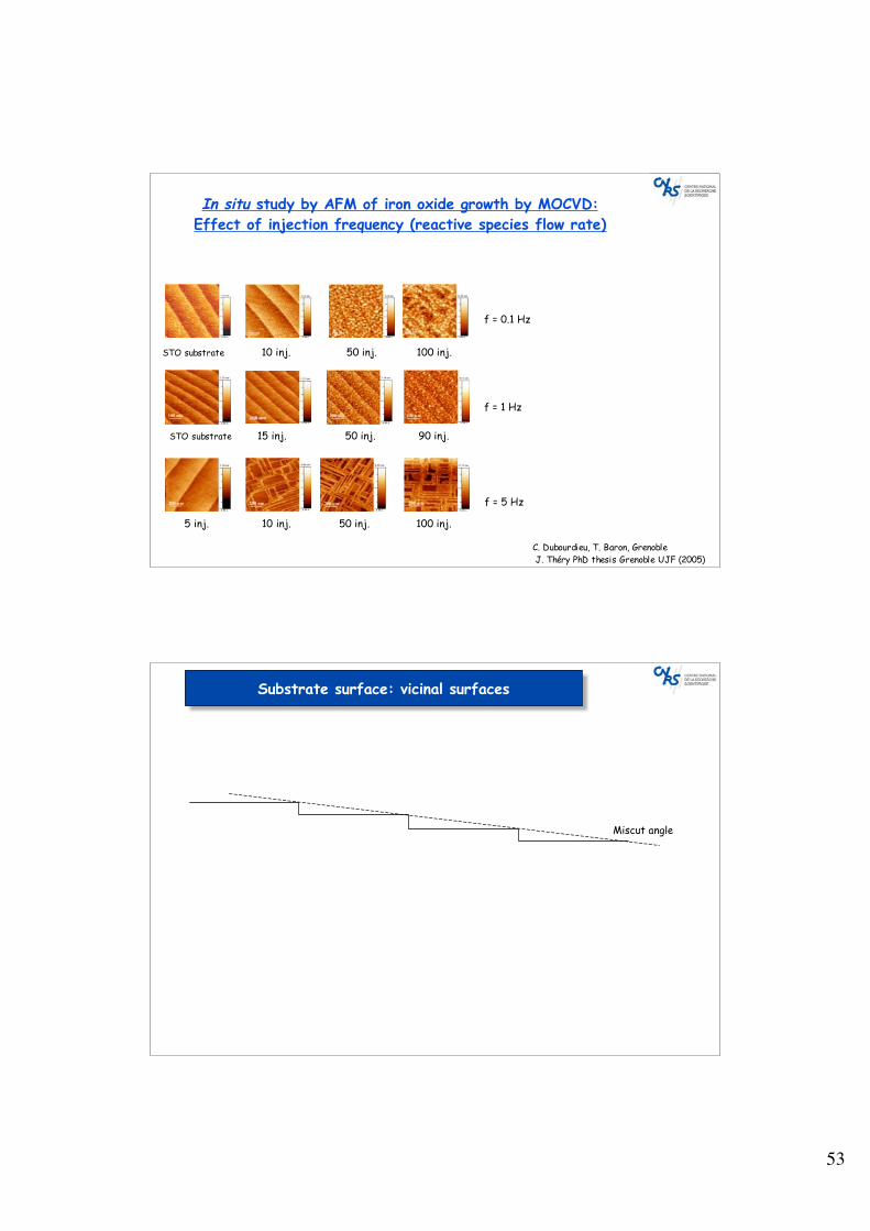
53
f = 0.1 Hz
f = 1 Hz
f = 5 Hz
5 inj. 10 inj. 50 inj. 100 inj.
15 inj. 50 inj. 90 inj.STO substrate
STO substrate 10 inj. 50 inj. 100 inj.
In situ study by AFM of iron oxide growth by MOCVD:Effect of injection frequency (reactive species flow rate)
C. Dubourdieu, T. Baron, Grenoble J. Théry PhD thesis Grenoble UJF (2005)
Substrate surface: vicinal surfaces
Miscut angle

54
= 0° and = 0° = 0.5° and = 0° = 1° and = 0° = 3° and = 45°
[001]
[010]
[100]
• By varying the vicinal angle of the substrate,we can induce drastic changes to theferroelectric domain structure
• We can effectively engineer BFO(001) to haveany type of domain structure we want
• Drawback Surface morphology is rougher
Controlling Domains – Vicinal Substrates
Courtesy Ramesh
Substrate surface: vicinal surfaces
Substrate surface orientation
* (001) SrTiO3: non polar BiFeO3 on SrTiO3 (001): what’s happen at the interface ??
(BiO)+ / (FeO2)- on (SrO) / ( TiO2) planes
* (001) LaAlO3: (LaO)+ / (AlO2)- polar planes: when stacking SrTiO3 with LaAlO3: how do charges distribute at interfaces ?? (H. Hwang et al.)
(110) LaAlO3: non polar surface
* Different surface orientation can be used to modify magnetic anisotropy for example (J. Fontcuberta)
55
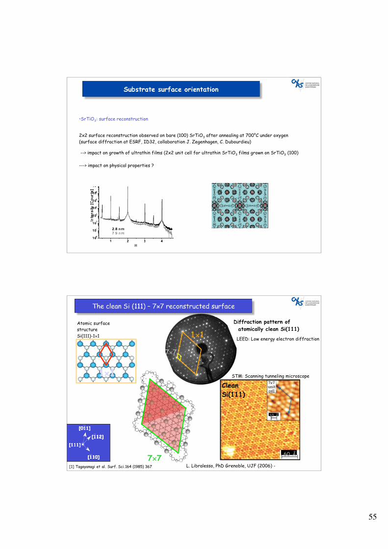
•SrTiO3: surface reconstruction
2x2 surface reconstruction observed on bare (100) SrTiO3 after annealing at 700°C under oxygen(surface diffraction at ESRF, ID32, collaboration J. Zegenhagen, C. Dubourdieu)
--> impact on growth of ultrathin films (2x2 unit cell for ultrathin SrTiO3 films grown on SrTiO3 (100)
---> impact on physical properties ?
Substrate surface orientation
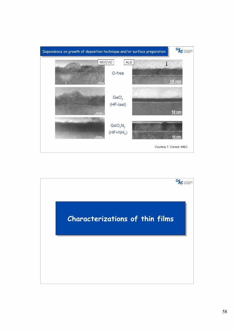
The clean Si (111) – 7 7 reconstructed surface
Diffraction pattern of atomically clean Si(111)
1 1
Atomic surfacestructureSi(111)-1 1
11 11
7 7
7 7
[111]
[110]
[112]
[011]
[111]
[110][110]
[112][112]
[011][011]
[1] Tagayanagi et al. Surf. Sci.164 (1985) 367
LEED: Low energy electron diffraction
CleanSi(111)
60 Å
10 Å
STM: Scanning tunneling microscope
L. Libralesso, PhD Grenoble, UJF (2006) -

56
2D smooth layers
Undisturbed Si(111) - 7 7 around the islands Pr2O3 : 2D triangular islands
STM study with increasing Pr2O3 film coverage
Homogenous island size : 150-20O Å Balance step flow + layer by layer growth
1.8 Å
200 Å
3.6 Å
400 Å 400 Å
12 Å
120 Å60 Å
L. Libralesso, PhD Grenoble, UJF (2006) -
STM
60 Å
LEED pattern (53eV)of Si(001) after
e-beam heating @ 1250°C
1 1
2 11 2
LEED
The clean Si (001) – 2 1 reconstructed surface
Si (001): 2x1 reconstructed surface
Growth of Pr2O3 on Si (001)
Baresubstrate
90° domains
90° domains
L. Libralesso, PhD Grenoble, UJF (2006) -

57
Courtesy T. Conard, IMEC
ALD of ZrO2 on HF-last Si: islands growth
Dependence of growth on surface preparation
Courtesy T. Conard, IMEC
Growth of HfO2 on Ge substrate
Dependence of growth on deposition technique and/or surface preparation
58
Courtesy T. Conard, IMEC
Dependence on growth of deposition technique and/or surface preparation
Characterizations of thin films

59
Substrate
FilmThickness
Composition (cations and oxygen content) - elemental profiles
Domains structure
Crystalline structure (average, distortions) - amorphous
Cations valence - Nature of bondings
Defects (vacancies, dislocations, twinnings…)
Substrate
Interfaces !!Nature of the interfaces
(composition, thickness….)
Physico-chemical & micro(nano)structural characterizationof thin films
mesoscopic, micrometric, nanometric
Thickness measurement : not trivial !
Mask part of the film: measure step height
X-ray reflectometry (XRR)
X-ray diffraction: fringes
Ellipsometry (spectroscopic): need optical properties of the materials
Transmission electron microscopy (destructive !)
XPS
…
Thickness determination

60
Composition measurement : not trivial
Energy Dispersive X-ray spectrometry (EDX) , Wavelength Dispersive X-ray spectroscopy (WDS): requires etalonsX-ray Fluorescence
X-ray photoelectron spectroscopy (XPS) or ESCA (Electron spectroscopy for composition analysis): Surface analysisComposition determination requires precise calibration from known composition sample analysis
Secondary Ions Mass Spectrometry (SIMS)
Rutherford Backscattering Spectrometry (RBS): no etalon
Oxygen stoichiometry: can not be precisely determined in thin films
However, oxygen stoichiometry drives/influences oxides properties !!!
(SrTiO3: becomes semiconducting if oxygen deficient…)
Composition determination
Crystalline structure determination
X-ray diffraction (reciprocal space mapping, various scans configurations…)For surfaces (interfaces): surface diffraction (need for synchrotron source)
Infra-red and Raman spectroscopies: very powerful to discriminate between different crystallinestructure and/or to evidence small lattice distortions that can sometimes not be detected by X-raydiffraction

61
Inte
nsi
ty (
arb
. u
nit
s)
LSMO3 6
/STO9 0
LSMO1 0 0
/STO9 0
LSMO2 1 0
/STO9 0
B
D
(b)
(a)
A
C
E
***
Raman spectroscopy:
e LSMO ~ 30/40 Å : orthorhombic
e LSMO ~ 100 Å : rhombohedral
(bulk structure)
J. Kreisel et al., J. Phys.: Cond Matter 14, (2002)
Raman spectroscopy:
10-4
10-3
10-2
10-1
100
101
55 60 65 70 75
I (a
.u.)
2 (deg.)
-1
-2
-3
-4-5
+1
+2
+3
+4
/2 scans at ESRF
X-ray diffraction (ESRF) /2 scans
d-spacings (out of plane)roughness at interfacesInterdiffusion
M. Nemoz et al., J. Appl. Phys. 100, 124110 (2006)
Crystalline structure ?
(La0.7Sr0.3MnO3/SrTiO3)15
Binding energy (eV)
No
rma
lize
d in
ten
sit
y
XPS analysis : determination of bonds and atoms environment - chemical selectivity
Y-O-Si / SiO2/Si stack
Growth of SiO2 and silicate favoredfor low species flow rate
SiO2: Si4+
Yttrium silicate: Si3+

62
A
AB
BCA
AB
BStacking fault
Twins
Dislocations
Defects identification
(dislocations, twins, GB, oxygen or cation vacancies, impurities…)
Optical microscopy
Transmission electron microscopy (local probe)
X-ray topography
EPR
…
YMnO3 / YSZ (111)HoMnO3 / Pt (111)
G. Van Tendeloo, EMAT, AnversC. Dubourdieu, LMGP

63
DyMnO32 nm
Blocks can beusually consideredas obtained by therotation by /3 andshift by ~c/6 (oronly shift by ~c/3)
Antiphase boundaries canbe generated by substratesteps and they can be alsoannihilated on stackingfaults
H.W. Zandbergen, Delft University - C. Dubourdieu, LMGP - A. Kaul Moscow (PhD of A. Bossak, INPG (2003))
Need to combine several characterization techniques
Different interactions (electrons/matter, ions/matter, photons/matter…)
Different probing lengths
Average information / local information

64
Many groups - see presentation of R. Ramesh (Monday) for an overview of state of the art research on BiFeO3
Group of R. Ramesh, Berkeley, US
J. Wang et al., Science 299, 1719 (2003)J. Wang et al. , Science 307, 1203b (2005)and many others !!! (lecture on Monday)
Group of A. Barthélémy & A. Fert, UMR CNRS-Thalès, Palaiseau, France
H. Bea, et al., Appl. Phys. Lett. 87, 072508 (2005), H. Béa et al., Appl. Phys. Lett. 88, 062502 (2005), H. Bea et al., Phys. Rev. B 74,020101(R) (2006) and much more…
M.G. Blamire, J.F. Scott, N.D. Mathur, Cambridge, UK: W. Eerenstein, et al. Science 307,1203a (2005)
Japanese group: K. Y. Yun, M. Noda, M. Okuyama, Appl. Phys. Lett. 83, 3981 (2003), K.Y. Yun, M. Noda, M. Okuyama, H. Saeki, H.Tabata, K. Saito, J. Appl. Phys. 96, 3399, (2004)
All PLD
BiFeO3 thin films
Chemical solution deposition: S. Iakovlev, C. H. Solterbeck, M. Kuhnke, M. Es-Souni, J. Appl. Phys. 97, 094901 (2005)
Sol gel: X. Qiet al., J. Mag. Mag. Mat. 283, 415 (2004)
Sputtering: Y. H. Lee et al., Electrochem. Solid-State Lett. 8, F55 (2005)
C. Ternon et al., Thin Solid Films 515, 481 (2006)
MOCVD:
Ramesh et al.: S.Y. Yang et al., Appl. Phys. Lett. 87, 102903 (2005) ----- > Monday lecture
C. Dubourdieu, LMGP - Grenoble J. Théry et al.,Proceedings of the Electrochem. Soc., Silicon Nitride and silicon dioxide thin insulating films anf other
emerginig dielectrics VIII, p. 498, (2005)J. Théry, et al., Chemical Vapor Deposition 13, 232 (2007)
BiFeO3 thin films

65
Bi-rich film
0.0
0.5
1.0
1.5
2.0
0.0 0.5 1.0 1.5 2.0 2.5
Bi/F
e m
ola
r ra
tio
in f
ilm (
Rf)
Bi/Fe molar ratio in solution (Rs)
Bi(mmp)3: R
f = 0.78 R
s
Bi(tmhd))3: R
f = 0.43 R
s
-100
-50
0
50
100
-10000 -5000 0 5000 10000
Mag
netizatio
n (em
u/c
m3)
Magnetic field (Oe)
XPS: Fe2+ presentFe3+ has multiple binding environment
Under-oxidised -Fe2O3 ?
BiFeO3 by MOCVD: difficult control of stoichiometry
Bi precursor highly sensitive to air ---> difficult control of stoichiometry
J. Théry et al. , Chemical Vapor Deposition 13, 232 (2007)
J. Dho, M.G. Blamire, Cambridge
J. Fontcuberta, Barcelona
K. Dörr, Halle
T. Noh, Seoul, Korea
N. Fujimura, Japan
C. Dubourdieu, France…
Exchange bias experiments (first papers in 2005)
Still many open questions for ReMnO3 thin films
Phase transitions in thin films ? Ordering temperatures ? Domains size … ?
Magnetoelectric effect ? (first order ME effect not possible in bulk)
Dependence of polarization on film thickness ? (possible enhancement of polarization through strain ?)
What governs leakage currents ?…
YMnO3, ReMnO3 thin films

66
C. Dubourdieu et al., Phil. Mag.Lett. 87, 203 (2007)
Bi2FeCrO6:
Ab initio calculation indicate multiferroism :
P. Baettig and N.A. Spalding, “Ab initio prediction of a multiferroic with large polarisation and magnetization”, Applied Physic Letters86, 012505 (2005)
Predicted to be multiferroic (P ~ 80 C/cm2)--- > attempts to prepare this compound as thin films
Group of A. Pignolet, INRS, Montreal, Canada
R. Nechache et al., “Growth, structure and properties of epitaxial thin films of first principles predicted multiferroic Bi2FeCrO6, Appl. Phys. Lett. 89, 102902 (2006)
A. Pignolet et al., “Epitaxial thin films of multiferroic with B-site cationic order”, Archiv - Cond. Matter
PLD films (Ts = 680°C, 9 mTorr O2) - post deposition anneal at 400°C
Fe3+/Cr3+ cation ordering necessary !!
Sr2FeMoO6: half metallic (fully spin-polarized), with Tc (ferromagnetic/paramagnetic) larger than room
temperature
Double-perovskite structure thin films

67
Bi2NiMnO6:
M. Sakai et al., , “Multiferroic thin film of with ordered double perovskite structure”, Appl. Phys. Lett. 90, 072903 (2005)
PLD films (Ts = 630°C, 0.4 Torr) - post deposition anneal at 450°C
Ferromagnetic behavior with Tc ~ 100 K and ferroelectric behavior with P ~ 5 C/cm2
Double-perovskite structure thin films
Tremendous progress in deposition techniques: sub-nanometer control of the growth of thin films
Crucial role of interfaces in the final properties: need to be precisely controlled
Physico-chemical characterization requires the combination of different techniques probing thesample at different scales and using different interaction types
(high-K oxides research field has triggered the development of suited metrologies)
Possibility to develop oxide heterostructures for new properties that will arise from interfaceseffects and from tailoring of charges, orbitals and spins couplings
Just the beginning as compared to the semiconductor heterostructures field !!
New phenomena will certainly come up in the future for oxides heterostructures
Combining oxides and semiconductors: take advantage of both --> new heterostructures
Conclusions and perspectives: