thin layers of transition metal oxides tjipke hibma materials science centre, university of...
Post on 20-Dec-2015
218 views
TRANSCRIPT
THIN LAYERS OF TRANSITION METAL OXIDES
Tjipke HibmaMaterials Science Centre, University of Groningen, The Netherlands
Contents
• Introduction to thin film deposition• Atomic layer-by-layer growth - Stoichiometry - Surface “chemistry” - Epitaxy - Morphology - Thickness
• Manipulation of properties, a few examples
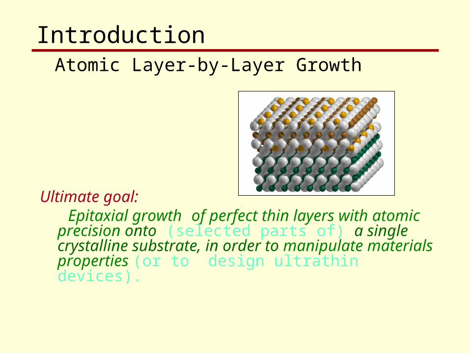
Ultimate goal: Epitaxial growth of perfect thin layers with
atomic precision onto (selected parts of) a single crystalline substrate, in order to manipulate materials properties (or to design ultrathin devices).
IntroductionAtomic Layer-by-Layer Growth
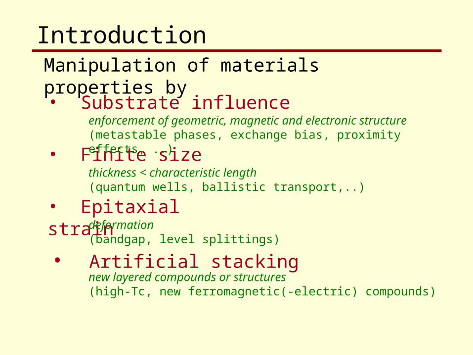
• Substrate influence
• Finite size
• Epitaxial strain
• Artificial stacking
enforcement of geometric, magnetic and electronic structure (metastable phases, exchange bias, proximity effects, ..)
thickness < characteristic length(quantum wells, ballistic transport,..)
deformation(bandgap, level splittings)
new layered compounds or structures(high-Tc, new ferromagnetic(-electric) compounds)
IntroductionManipulation of materials properties by
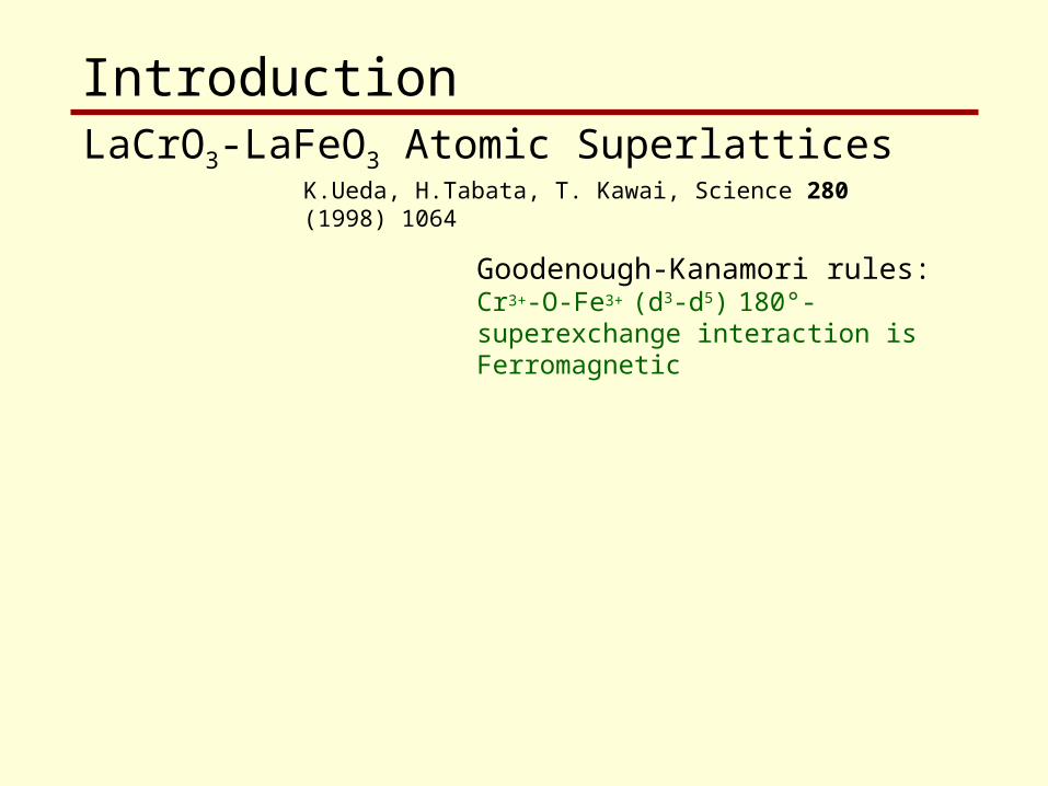
K.Ueda, H.Tabata, T. Kawai, Science 280 (1998) 1064
Goodenough-Kanamori rules:Cr3+-O-Fe3+ (d3-d5) 180°-superexchange interaction is Ferromagnetic
LaCrO3-LaFeO3 Atomic Superlattices
Introduction
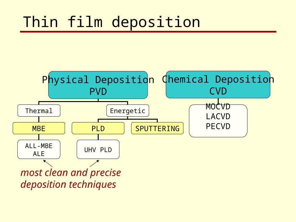
Physical DepositionPVD
Thermal Energetic
MBE PLD SPUTTERING
ALL-MBEALE
UHV PLD
Chemical DepositionCVD
MOCVDLACVDPECVD
Thin film deposition
most clean and precise deposition techniques
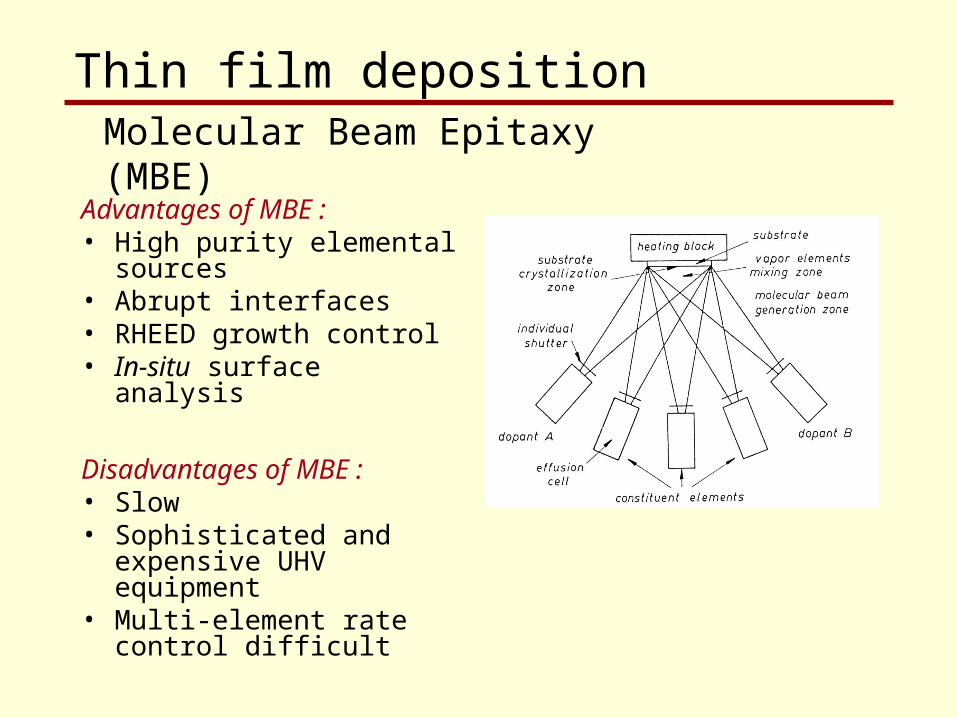
Advantages of MBE :• High purity elemental
sources• Abrupt interfaces • RHEED growth control • In-situ surface analysis
Disadvantages of MBE : • Slow• Sophisticated and
expensive UHV equipment
• Multi-element rate control difficult
Thin film depositionMolecular Beam Epitaxy (MBE)
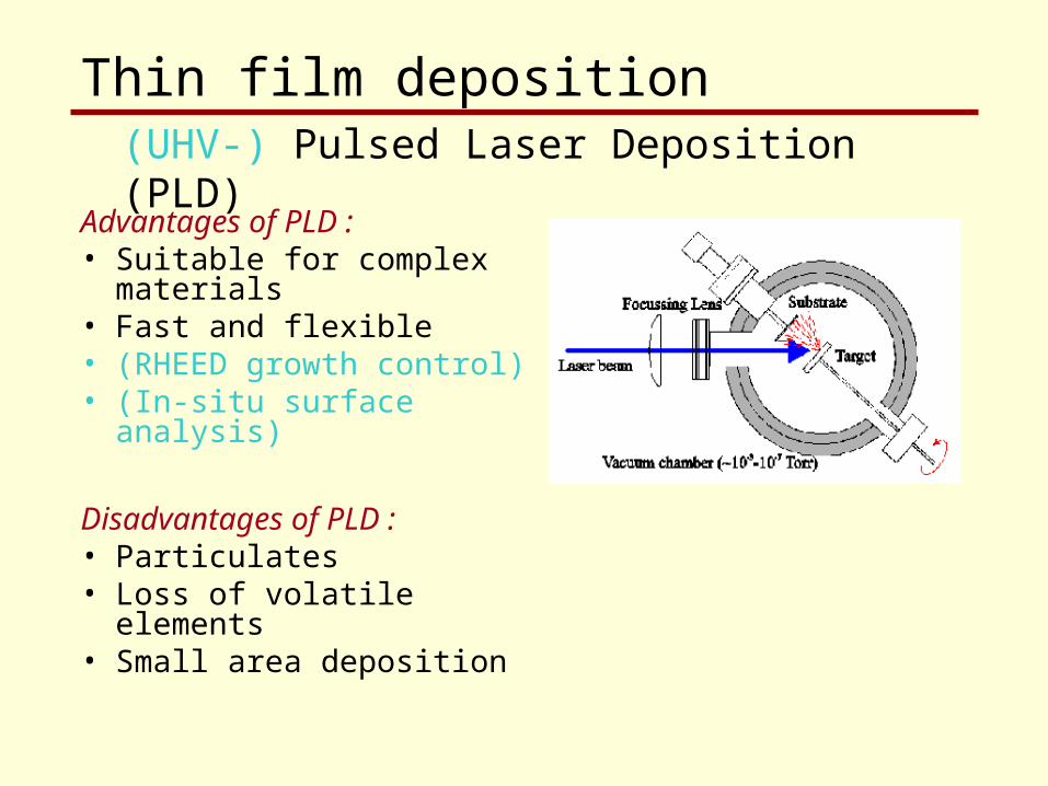
Advantages of PLD :• Suitable for complex
materials • Fast and flexible• (RHEED growth control) • (In-situ surface analysis)
Disadvantages of PLD : • Particulates• Loss of volatile elements• Small area deposition
Thin film deposition(UHV-) Pulsed Laser Deposition (PLD)
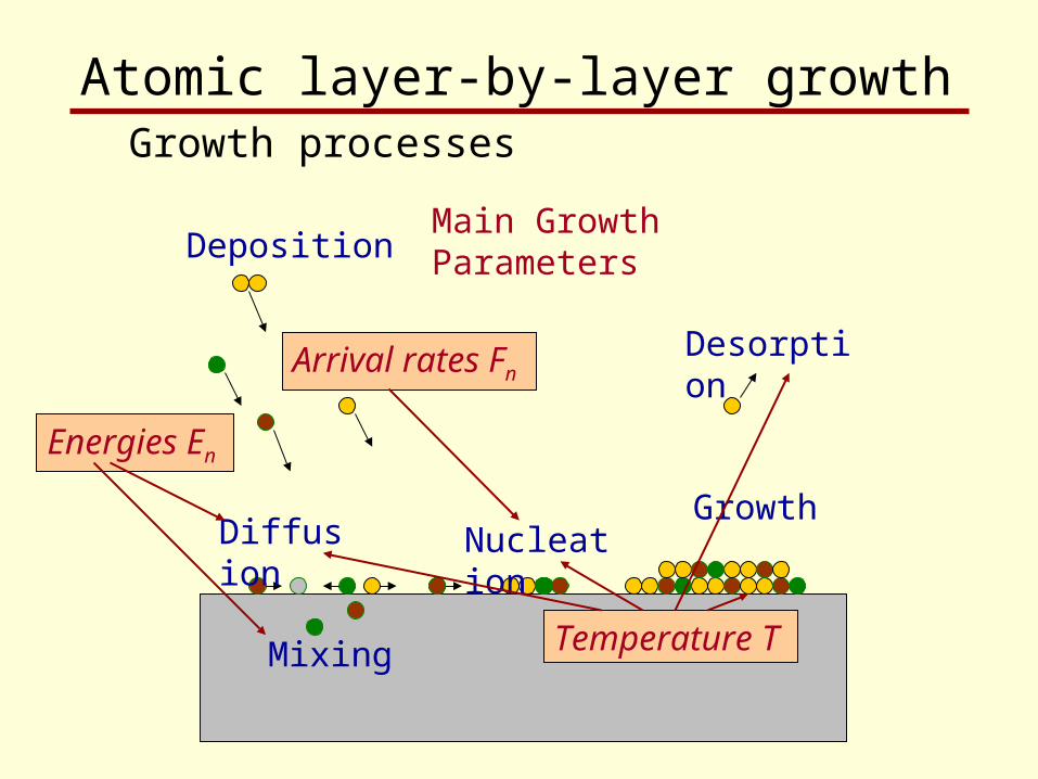
Deposition
Diffusion NucleationGrowth
Desorption
Mixing
Arrival rates Fn
Temperature T
Main Growth Parameters
Energies En
Atomic layer-by-layer growthGrowth processes
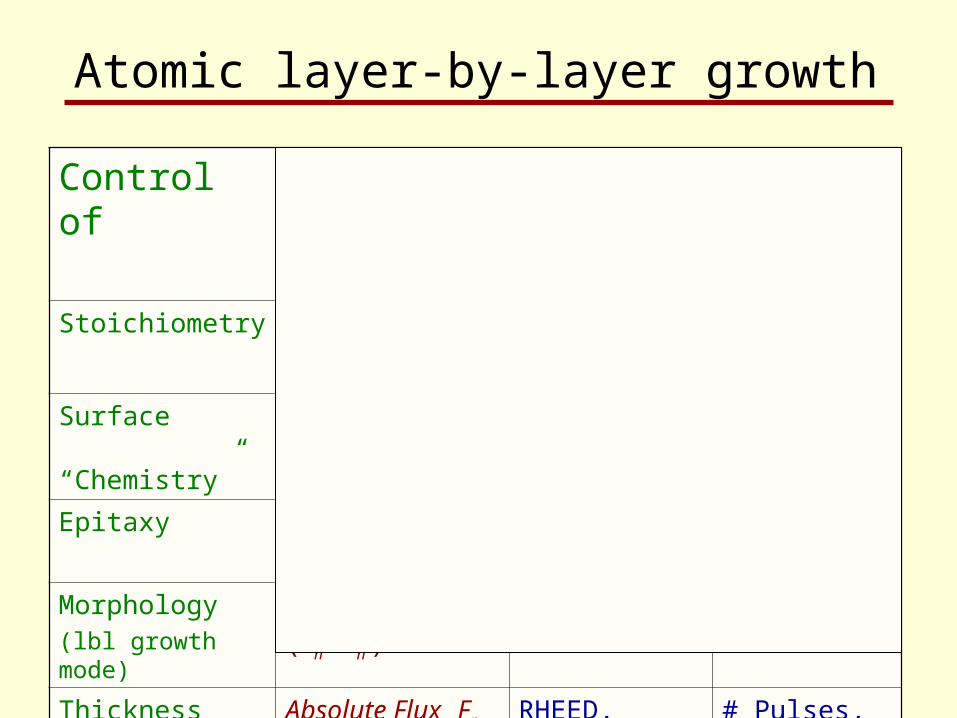
Control of GrowthParameters
MBE PLD
Stoichiometry Relative Flux FnDifficult for n>2, ALL-MBE
Loss of volatile components.
Surface “Chemistry”
Temperature T Energies En
Tsubstrate
thermal <0.1 eV
Tsubstrate
0.1-10eV (Pback)
Epitaxy Substrate
Morphology(lbl growth mode)
Nucleation rate(Fn/Dn )
RHEED (RHEED)
Thickness(nr of layers)
Absolute Flux Fn RHEED, ALE
# Pulses,(RHEED)
Atomic layer-by-layer growth
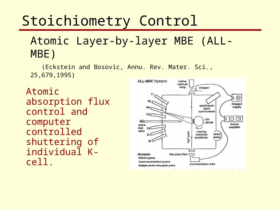
Atomic Layer-by-layer MBE (ALL-MBE) (Eckstein and Bosovic, Annu. Rev. Mater. Sci., 25,679,1995)
Stoichiometry Control
Atomic absorption flux control and computer controlled shuttering of individual K-cell.
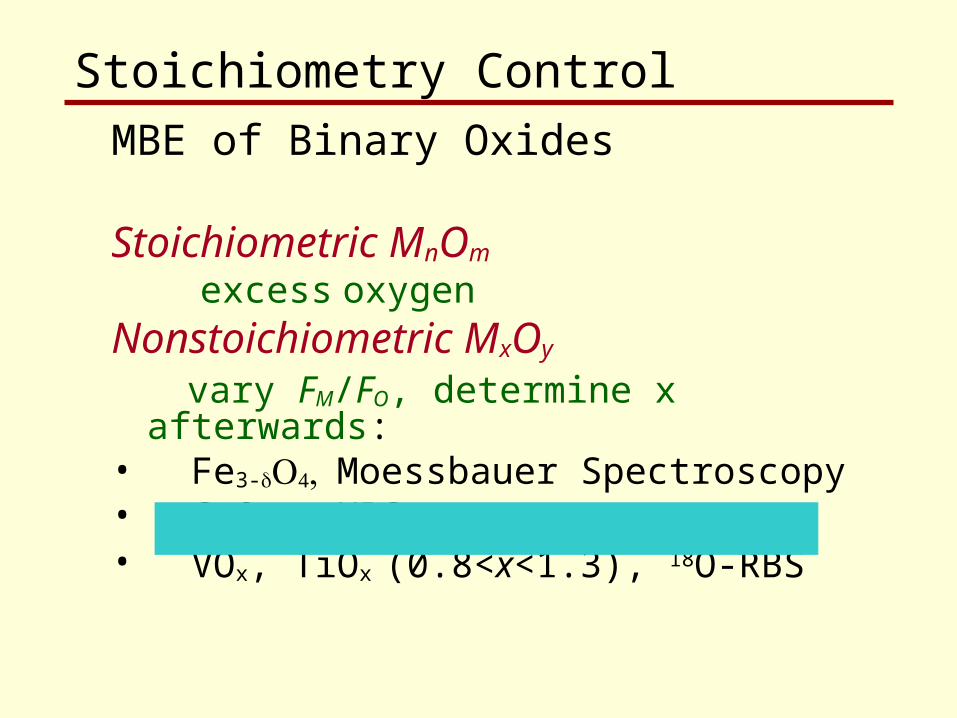
MBE of Binary Oxides
Stoichiometric MnOm
excess oxygen Nonstoichiometric MxOy
vary FM/FO, determine x afterwards:• Fe3-Moessbauer Spectroscopy• CrOx , XPS• VOx, TiOx (0.8<x<1.3), 18O-RBS
Stoichiometry Control
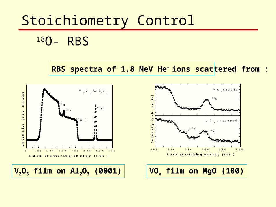
0 1 0 0 2 0 0 3 0 0 4 0 0 5 0 0 6 0 0 7 0 0
V2
O3
/ A l2
O3
2 7 A l
1 6 O1 8 O
5 1 V
In
te
ns
ity
(a
rb
.un
its
)
B a c k s c a t t e r i n g e n e r g y ( k e V )
2 0 0 2 2 0 2 4 0 2 6 0 2 8 0 3 0 0
1 6 O 1 8 O
V Ox
u n c a p p e d
In
te
ns
ity
(a
rb
. u
nit
s)
B a c k s c a t t e r i n g e n e r g y ( k e V )
1 8 O
V Ox
c a p p e d
V2O3 film on Al2O3 (0001) VOx film on MgO (100)
RBS spectra of 1.8 MeV He+ ions scattered from :
18O- RBS
Stoichiometry Control
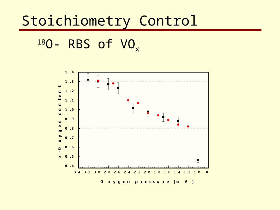
3 4 3 2 3 0 2 8 2 6 2 4 2 2 2 0 1 8 1 6 1 4 1 2 1 0 8
0 . 4
0 . 5
0 . 6
0 . 7
0 . 8
0 . 9
1 . 0
1 . 1
1 . 2
1 . 3
1 . 4
x-
Ox
yg
en
co
nt
en
t
O x y g e n p r e s s u r e ( m V )
Stoichiometry Control18O- RBS of VOx
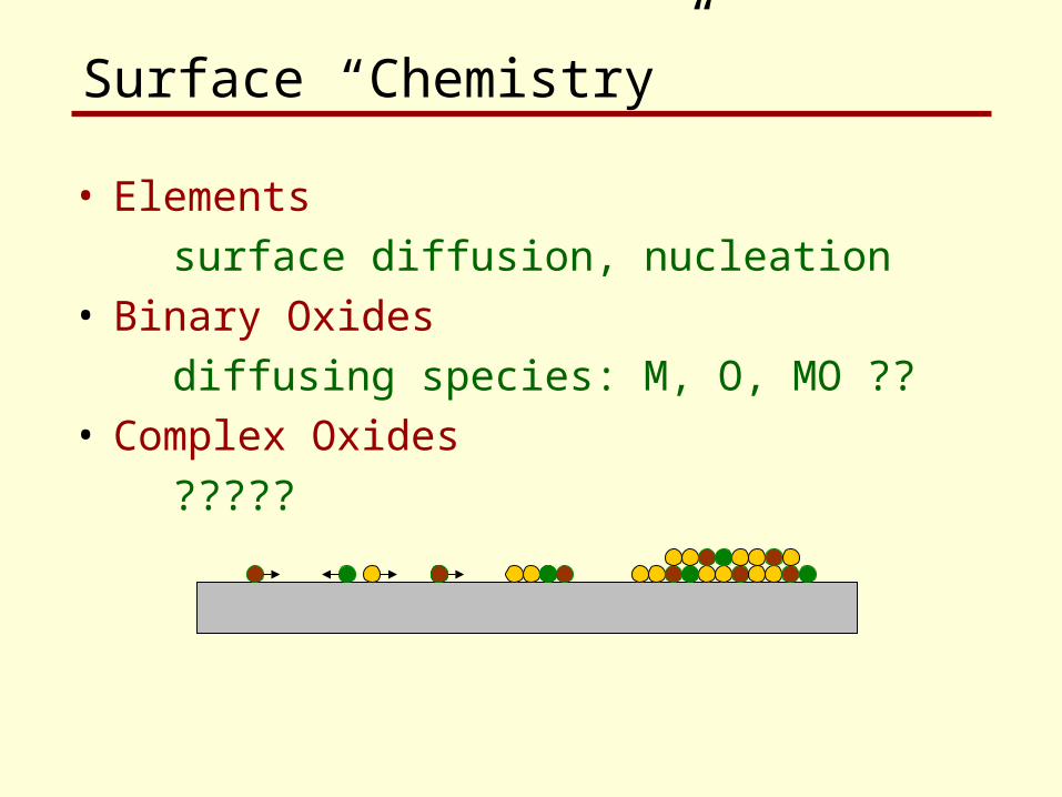
• Elements surface diffusion, nucleation• Binary Oxides diffusing species: M, O, MO ??• Complex Oxides ?????
Surface “Chemistry”
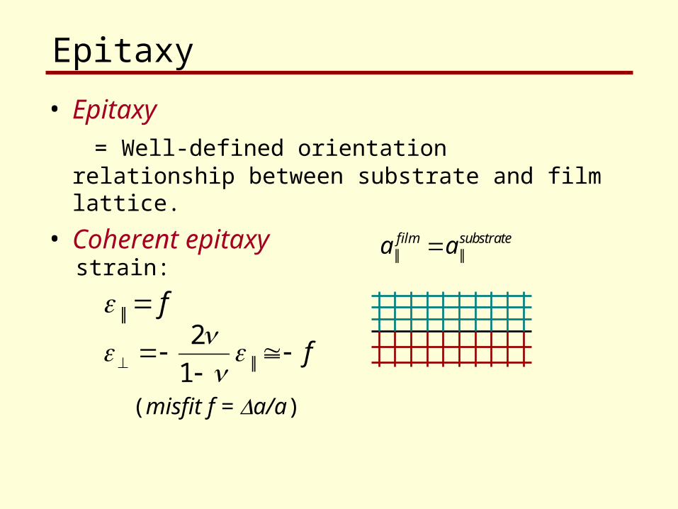
• Epitaxy = Well-defined orientation relationship
between substrate and film lattice.
• Coherent epitaxya afilm substrate
|| ||strain:
|| f
(misfit f = a/a)
Epitaxy
2
1 || f
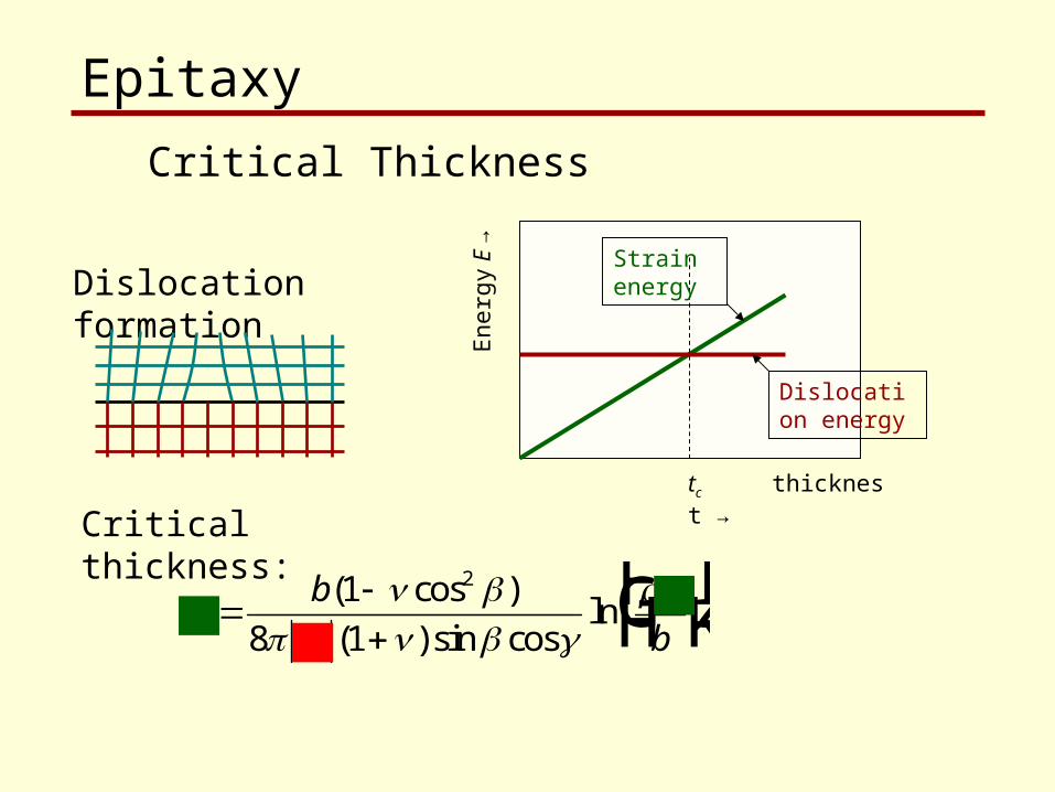
Dislocation formation
Critical thickness:
tb
f
t
bco
c
FHG
IKJ
( cos )
( ) sin cosln
1
8 1
2
Epitaxy
Critical Thickness
Dislocation energy
Strain energy
tc thicknes t →Energ
y E
→
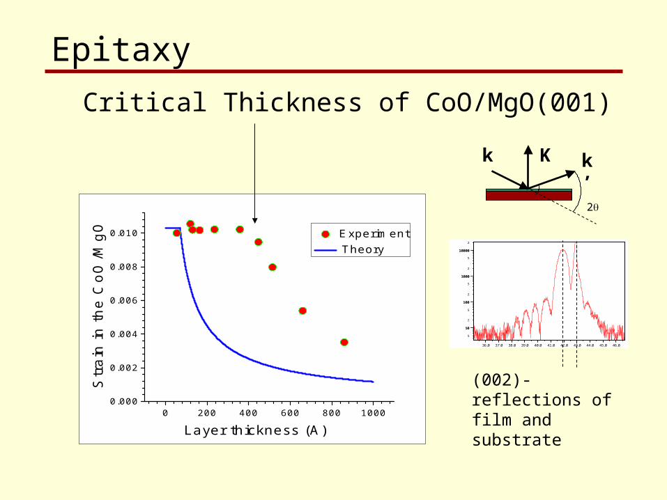
Epitaxy
Critical Thickness of CoO/MgO(001)
0 200 400 600 800 10000.000
0.002
0.004
0.006
0.008
0.010
Str
ain
in t
he
Co
O/M
gO
Layer thickness (A)
Experiment Theory
36.0 37.0 38.0 39.0 40.0 41.0 42.0 43.0 44.0 45.0 46.0
5
10
2
5
100
2
5
1000
2
5
10000
2
(002)- reflections of film and substrate
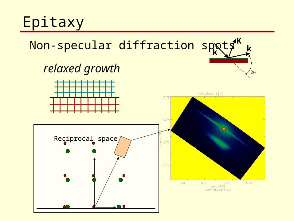
k k’K
2
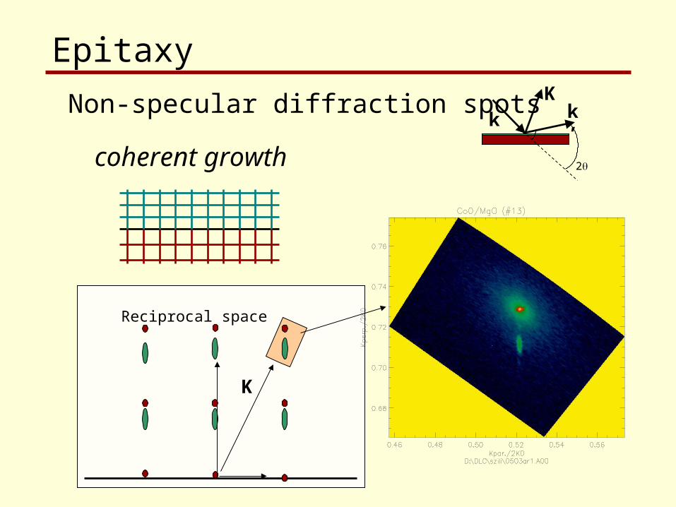
Reciprocal space
K
coherent growth
Epitaxy
Non-specular diffraction spotsk k’
K
2
Reciprocal space
Epitaxy
Non-specular diffraction spots
relaxed growth
k k’K
2
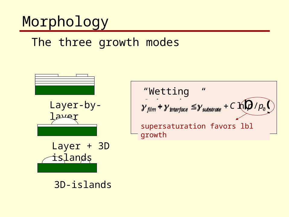
Layer-by-layer
Layer + 3D islands
3D-islands
The three growth modes
“Wetting Criterion” film erface substrate C p p int ln / 0b gsupersaturation favors lbl growth
Morphology
film erface substrate int
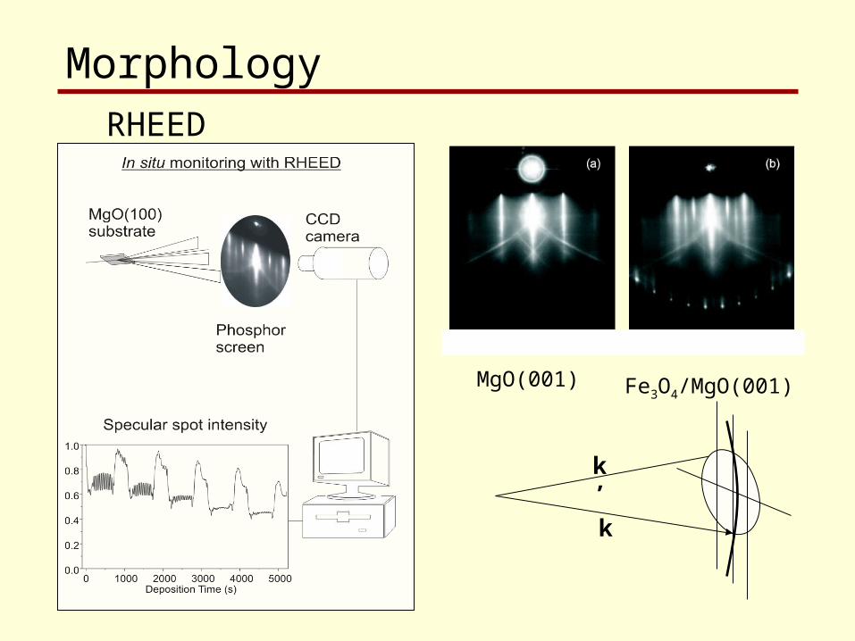
MgO(001) Fe3O4/MgO(001)
MorphologyRHEED
k
k’
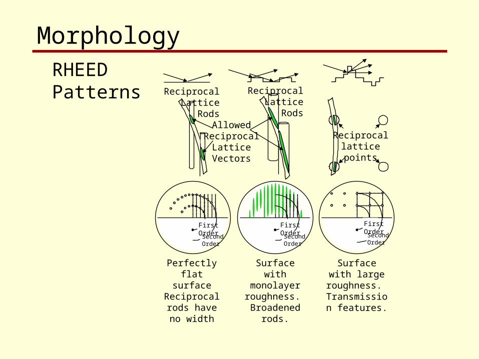
ReciprocalLattice
Rods
Reciprocallatticepoints
Perfectly flat surface
Reciprocal rods have no
width
Surface with monolayer roughness. Broadened
rods.
Surface with large
roughness. Transmission
features.
ReciprocalLattice
RodsAllowed
ReciprocalLattice Vectors
FirstOrderSecondOrder
FirstOrderSecondOrder
FirstOrderSecondOrder
MorphologyRHEEDPatterns
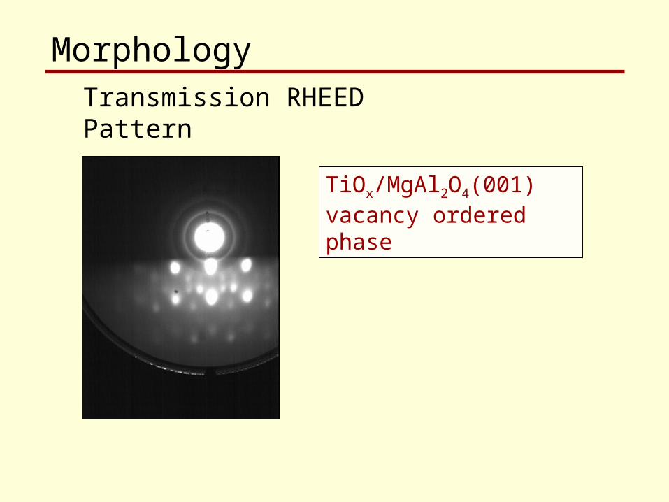
TiOx/MgAl2O4(001)vacancy ordered phase
MorphologyTransmission RHEED Pattern
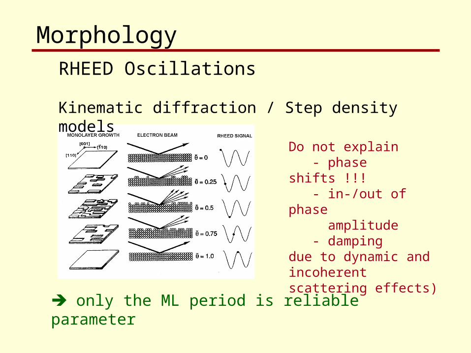
Kinematic diffraction / Step density models
Do not explain - phase shifts !!! - in-/out of phase amplitude - damping due to dynamic and incoherent scattering effects)
only the ML period is reliable parameter
MorphologyRHEED Oscillations
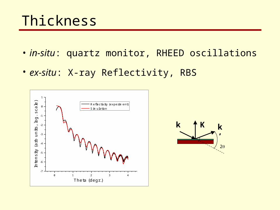
Thickness
• in-situ: quartz monitor, RHEED oscillations
• ex-situ: X-ray Reflectivity, RBS
0 1 2 3 4-7
-6
-5
-4
-3
-2
-1
0
1
Inte
nsity
(ar
b un
its,
log.
sca
le)
Theta (degr.)
Reflectivity (experiment) Simulation
k k’K
2
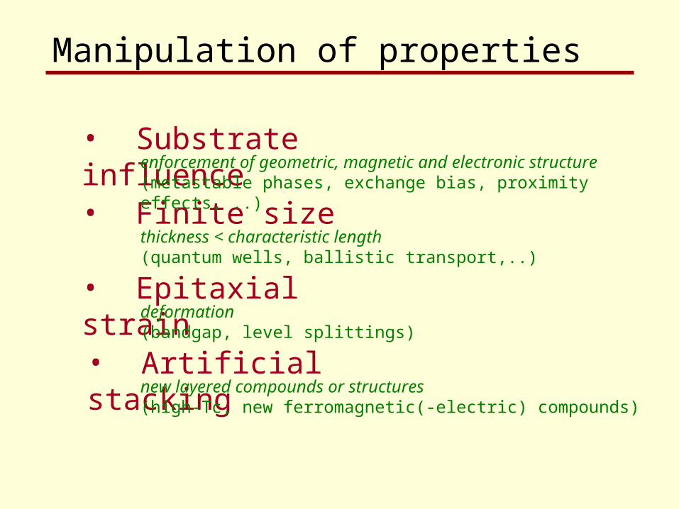
• Substrate influence
• Finite size
• Epitaxial strain
• Artificial stacking
enforcement of geometric, magnetic and electronic structure (metastable phases, exchange bias, proximity effects, ..)
thickness < characteristic length(quantum wells, ballistic transport,..)
deformation(bandgap, level splittings)
new layered compounds or structures(high-Tc, new ferromagnetic(-electric) compounds)
Manipulation of properties
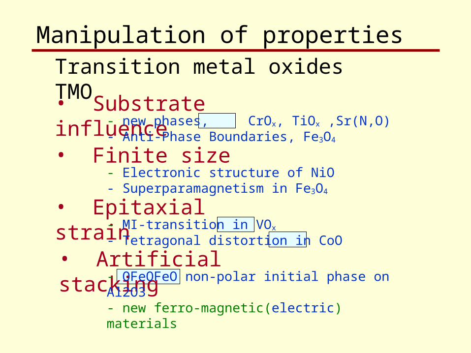
• Substrate influence
• Finite size
• Epitaxial strain
• Artificial stacking
- new phases, CrOx, TiOx ,Sr(N,O)- Anti-Phase Boundaries, Fe3O4
- Electronic structure of NiO- Superparamagnetism in Fe3O4
- MI-transition in VOx
- Tetragonal distortion in CoO
- OFeOFeO non-polar initial phase on Al2O3- new ferro-magnetic(electric) materials
Manipulation of propertiesTransition metal oxides TMO
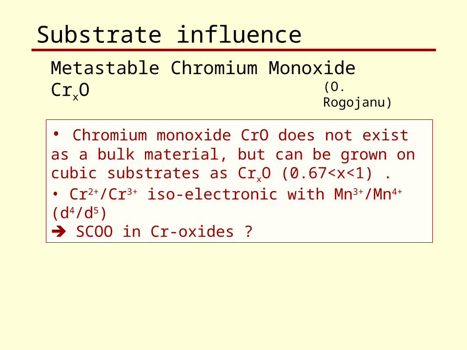
• Chromium monoxide CrO does not exist as a bulk material, but can be grown on cubic substrates as CrxO (0.67<x<1) .• Cr2+/Cr3+ iso-electronic with Mn3+/Mn4+ (d4/d5) SCOO in Cr-oxides ?
(O. Rogojanu)
Substrate influence Metastable Chromium Monoxide CrxO
ab
c
xy
z
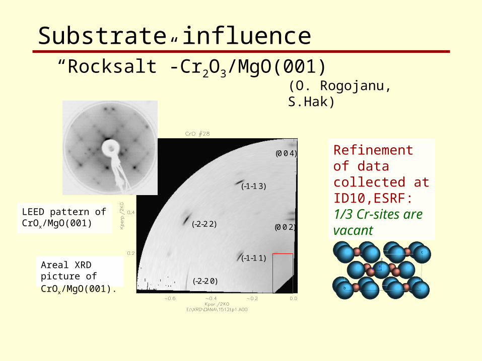
Areal XRD picture of CrOx/MgO(001).
LEED pattern of CrOx/MgO(001)
(-1-1 1)
(0 0 2) (-2-2 2)
(-1-1 3)
(-2-2 0)
(0 0 4) Refinement of data collected at ID10,ESRF:1/3 Cr-sites are vacant
(O. Rogojanu, S.Hak)“Rocksalt”-Cr2O3/MgO(001)
Substrate influence
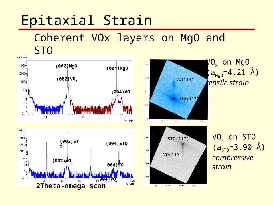
VOx on STO(aSTO=3.90 Å)compressive strain
MgO(113)MgO(113)
VO(113)
(002)MgO
(002)VOx
(004)MgO
(004)VOx
(002)VOx
(004)VOx
(002)STO (004)STO
VO(113)
STO(113)
2Theta-omega scan
VOx on MgO(aMgO=4.21 Å) tensile strain
Epitaxial Strain Coherent VOx layers on MgO and STO
(004)VOx
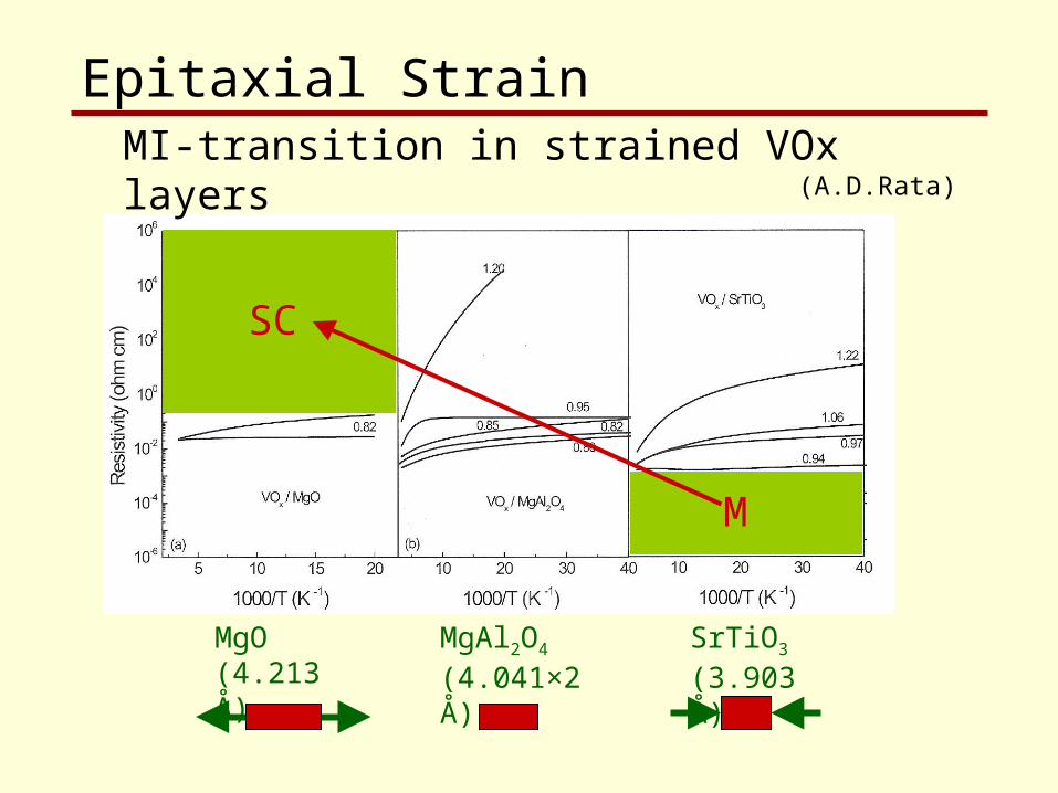
(A.D.Rata)
SrTiO3
(3.903 Å)MgAl2O4
(4.041×2 Å)
MgO(4.213 Å)
M
SC
Epitaxial Strain MI-transition in strained VOx layers
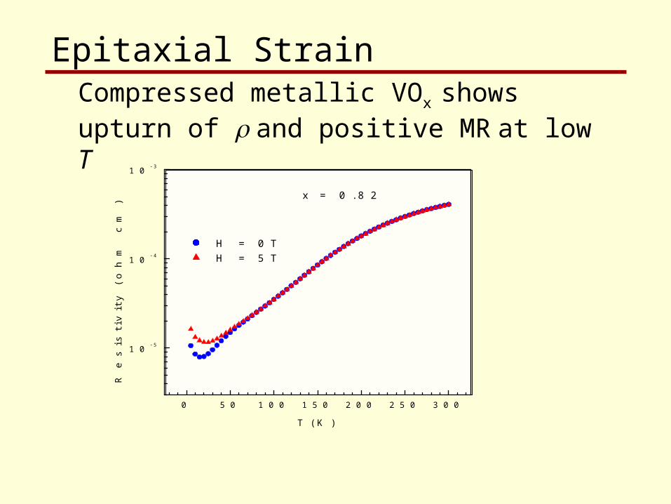
0 5 0 1 0 0 1 5 0 2 0 0 2 5 0 3 0 0
1 0 - 5
1 0 - 4
1 0 - 3
x = 0 . 8 2
H = 0 T H = 5 T
Re
sis
tiv
ity
(o
hm
cm
)
T ( K )
Epitaxial Strain Compressed metallic VOx shows upturn of and positive MR at low T
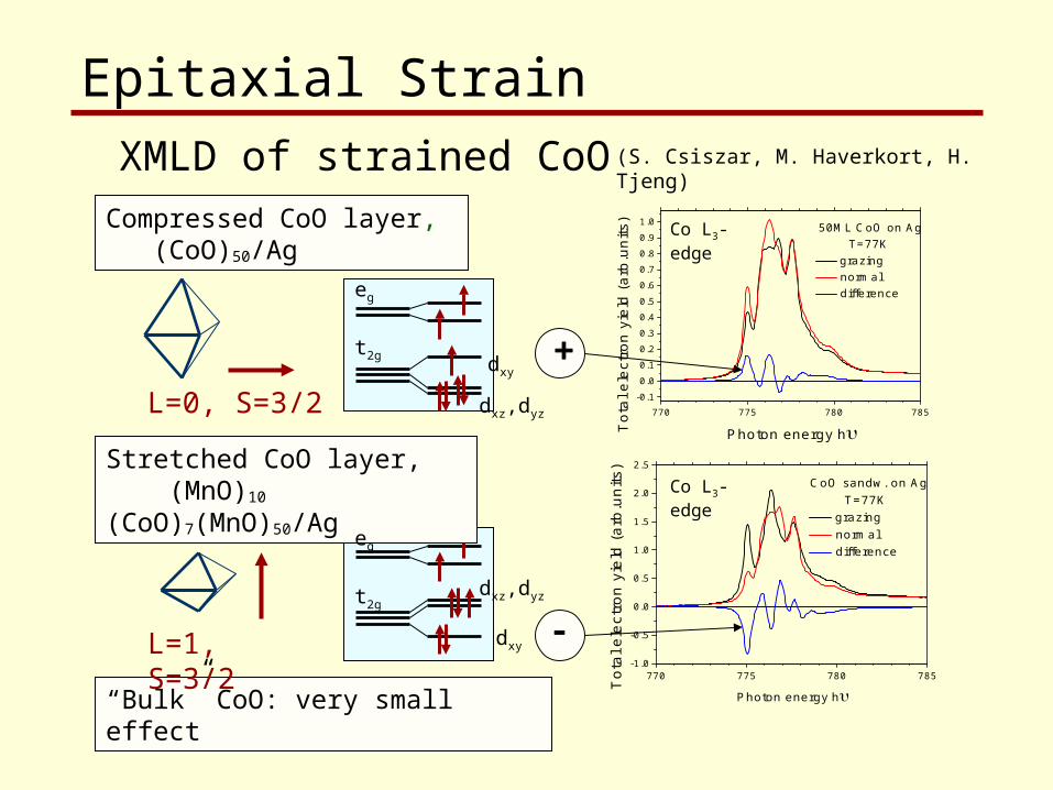
770 775 780 785-0.1
0.0
0.1
0.2
0.3
0.4
0.5
0.6
0.7
0.8
0.9
1.0
T
otal
ele
ctro
n yi
eld
(arb
.uni
ts)
Photon energy h
50ML CoO on AgT=77K
grazing normal difference
770 775 780 785-1.0
-0.5
0.0
0.5
1.0
1.5
2.0
2.5
T
ota
l ele
ctro
n y
ield
(a
rb.u
nits
)
Photon energy h
CoO sandw. on AgT=77K
grazing normal difference
Compressed CoO layer, (CoO)50/Ag
Stretched CoO layer, (MnO)10 (CoO)7(MnO)50/Ag
“Bulk” CoO: very small effect
L=1, S=3/2
L=0, S=3/2
Epitaxial Strain XMLD of strained CoO (S. Csiszar, M. Haverkort, H. Tjeng)
Co L3-edge
Co L3-edge
t2g
t2g
eg
eg
dxz,dyz
dxz,dyz
dxy
dxy
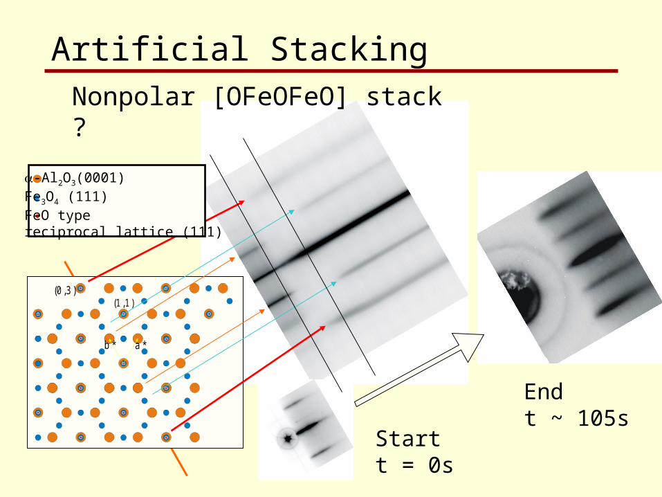
(0 ,3)(1 ,1)
b * a *
Endt ~ 105s
-Al2O3(0001)Fe3O4 (111)FeO typereciprocal lattice (111)
Artificial Stacking Nonpolar [OFeOFeO] stack ?
Startt = 0s
Final remarks
• The ideal of atomic layer-by-layer growth can be approached using MBE and UHV-PLD techniques.
However,
• Control of stoichiometry, completeness and structure of atomic layer during growth is still unsatisfactory.
• Knowledge of surface “chemistry” is almost fully lacking.
• Postgrowth characterisation of composition and structure is a tedious and tough job.
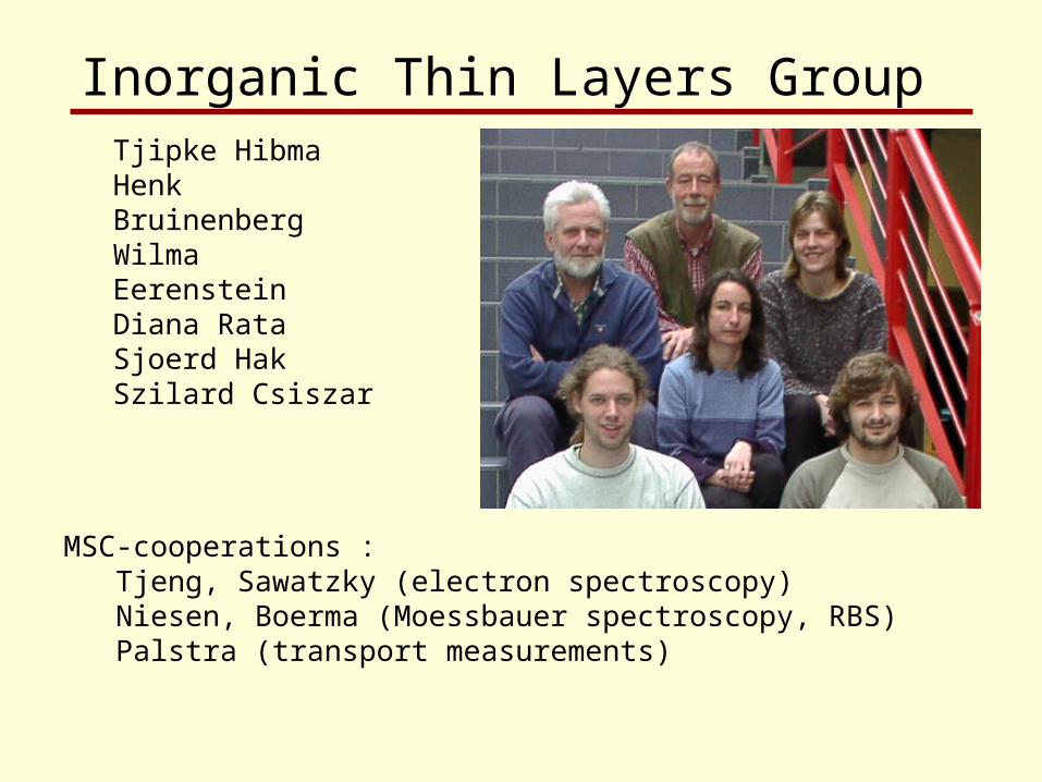
Tjipke HibmaHenk BruinenbergWilma EerensteinDiana RataSjoerd HakSzilard Csiszar
MSC-cooperations : Tjeng, Sawatzky (electron spectroscopy) Niesen, Boerma (Moessbauer spectroscopy, RBS) Palstra (transport measurements)
Inorganic Thin Layers Group