this document has been reproduced from … · uric las g3/33 31843 final report ... to damage from...
TRANSCRIPT

N O T I C E
THIS DOCUMENT HAS BEEN REPRODUCED FROM MICROFICHE. ALTHOUGH IT IS RECOGNIZED THAT
CERTAIN PORTIONS ARE ILLEGIBLE, IT IS BEING RELEASED IN THE INTEREST OF MAKING AVAILABLE AS MUCH
INFORMATION AS POSSIBLE
https://ntrs.nasa.gov/search.jsp?R=19810019817 2018-06-25T08:39:00+00:00Z

(NASA-CR-161827) CHARGE INJECTION DEVICE N81 -1$355EVALUATION HARDWARE PiLdl Report (BendixCorp.) 17 p HC A011+if Air 1 CSCL U9C
uric lasG3/33 31843
FINAL REPORTCHARGE INJECTIONDEVICE EVALUATION
HARDWARE
CONTRACT NO.NAS 8-33740
Prepared for:
George C. MarshallSpace Flight CenterAlabama 35812
April 30, 1981
^^^^ 16^ 89c'
A UG 1981
v, RECEI VEDco Nft
Alft sn Fm
rD&r
THE BENDIX CORPORATIONGUIDANCE SYSTEMS DIVISION
TETERBORO, NEW JERSEY 07608
V,& - -

1.0 INTRODUCTION
Star trackers typically employ photomultiplier/image
dissector type devices as detection sensors. These
devices are large and bulky, adding weight and volume
to end-item physical characteristics. They require
thousands of volts bias for proper operation, thereby
necessitating use of proper protection at the detector
tube and power supply level to guard against potential,
catastrophic arcing problems in a space environment. They
require magnetic shielding and a shutter mechanism for
photocathode protection against possible sunlight damage.
Better versatility and flexibility would be achieved if
solid state detectors could be utilized as alternate devices.
They are small and light, requiring only a few volts
reverse bias at almost zero power. They do not need magnetic
shielding of any kind and they have sufficient sensitivity
characteristics to make them candidates for star sensor
applications and, most important, they are not susceptible
to damage from high light levels. They can survive when
the sun is focussed directly onto them and can tolerate
being heated by such means to several hundred degrees
centigrade without permanent damage. Charge Injection
Devices (CID's) appear to promise this capability.
2.0 OBJECTIVE
The objective of this effort was to develop a versatile
test tool to evaluate candidate CID detectors. This
resulted in the design and fabrication of a microprocessorr based system which provides maximum testing flexibility via
f '

L'
fr
software reconfiguration. This system has the capability to
evaluate a charge injection device (CID) and to characterize
its performance. The construction and operation of the Ci!1
offers several significant advantages over the various CCD
configurations currently available. Among these advantages
are:
o Less sophisticated manufacturing processes required
than for CCD's. Results in potentially lower
fabrication costs and higher yields.
o Virtually no obscuration (i.e., dead zones) between
pixels (interline transfer CCD3 have 50`b) results
in high optical gain and no distortion of the inter-
polation function.
o No image smearing during readout (as in frame transfer
CCD's) allows continuous exposure without shettering
the optical input.
o High resistance to blooming due to optical overload
permits detection of dim targets near bright sources.
o Nigh transfer efficiencies (i.e., >0.999) not required
due to low (by several orders of magnitude compared
to CCD's) number of transfer operations required to
read a pixel.
o Insensitivity to transfer efficiency variations
provides improved tolerance to degradation mechanisms
(e.g., radiation).
2

13.0 CHARGE INJECTION DEVICE (CID) CONFIGURATION
The CID is organized as an array of 128 by 128 picture
elements (pixels). A 30um pixel spacing provides an active
photosensitive area of about 0.145 sq. cm . A simplified
CID layout is shown in Figure 1.
The array is divided into 1024 blocks, each consisting of4x4 pixels. Any given block is selected via on -chiphorizontal (column) and vertical (row) shift registers.
Enable lines (E1 through E4) transfer signal charge for a
single column from pixel collection sites to corresponding
output sites. Signals from all four rows are available
simultaneously (parallel outputs) for processing.
` Subsequent rows are read-out by first returning the signal
j charge for the current row back to the collection site and
{ then transferring the signal for the next row. This non-
destructive readout method is continued until all of theiI desired blocks have been interrogated. At this point, all
of the signal charge in the entire array is injected into
the substrate to reset the collection sites for the next1
integration period'(frame.).
The above CID readout method is but one of several possible
alternatives made available by the configuration of the
device to by evaluated. This, in part, is due to the
relatively large number of control lines brought to the
external pinout.
Due to its unique timing and voltage level requirements,
evaluation of the CID in a previously constructed CCD
breadboard was not possible without extensive modification.
3

#2V Q 0 o 1 2Y 05 04 03 02 01 Vq0
r-------0cvo RVD
----ti RVG
E E2
- `V
VIN ID IG HIN
ROUT
FIGURE 1
128 X 128 CID CONFIGURATION
4
Li

Furthermore, the exploration of various readout methods
and processing techniques may require additional complex
circuitry. Thus a separate CID breadboard, under the
control of a microprocessor, will provide a more expedient
approach to device evaluation.
4.0 CID BREADBOARD
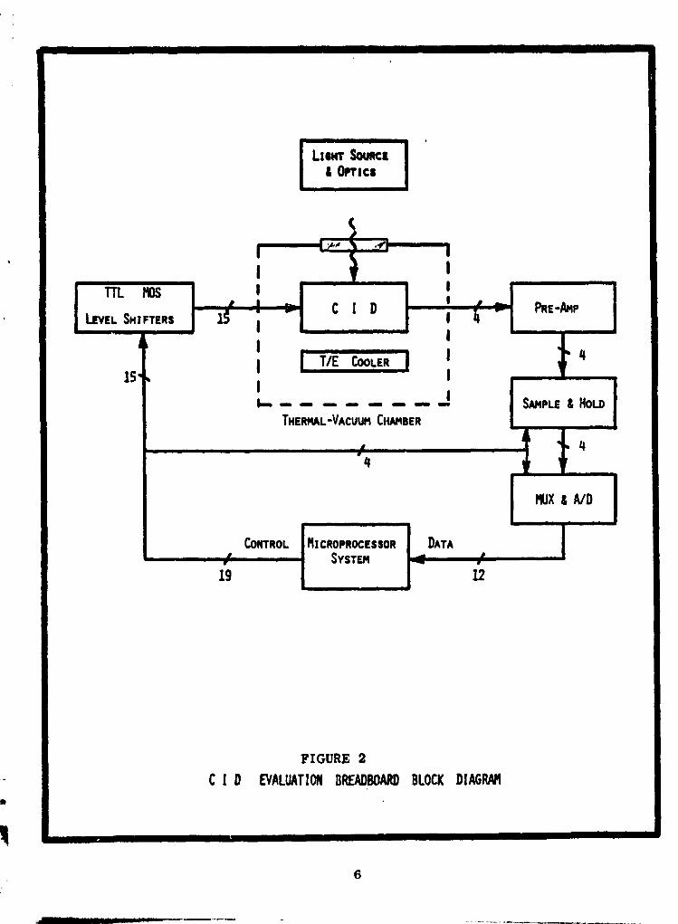
A block diagram of the CID breadboara is shown in Figure 2.
The micro-processor (VP) based test configuration provides
maximum flexibility to explore various CID readout and
signal processing techniques.
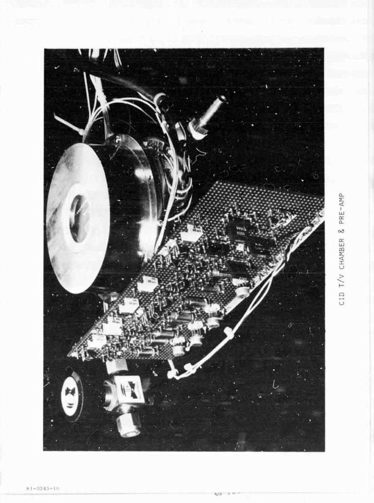
The CID is housed in a small thermal-vacuum chamber to
provide a controlled temperature environment. An optical
window on the chamber passes light from an external test
source/imaging assembly to the photo-sensitive array. The
control signals required to operate the CID are generated
by the microprocessor under software control. Level shifters
are required to convert the TTL logic levels to appropriate
MOS values.
The signal processing electronics consist of four high
gain, low-noise preamplifiers, companion sample-and-hold
(S/H) circuits and a multiplexed analog-to-digital ( A /D)
converter. This configuration is necessary to convert
the parallel CID output to a serial VP input.
C5
Emoa
a
I ^TTL MOS 1 1
LEVEL SNIFTERS is' C I D
1
1WE COOLER
15 I
— — — — — -w mom 1
THERMAL-VACUUM CHAMBER
is4
PRE-AMP
4
SAMPLE i HOLD
4
MUX i A/D
CONTROL MICROPROCESSORkt"
12
SYSTEM
19
FIGURE 2
C I D EVALUATION BREADBOARD BLOCK DIAGRAM
8

mQOWQQWw
ZO
F-a
JQW
Q
ORICUNAL PAGE IS
' dF N)''R QUALITY
Hi-0345-6
, I

MICROPROCESSOR
The CID evaluation breadboard incorporates a microprocessor
to perform three distinct tasks: 1. CID/Electronics control,
2. Data Collection, 3. Data Processing. Control and
collection operations are shared during a given test in
real time whereas processing is performed "off-line" after
sufficient data is collected.
A block diagram of the microprocessor and support equipment
is shown in Figure 3. A single board computer (Rockwell
AIM65) utilizes a 6502 microprocessor operating at one
megahertz. Buildin serial I/O is used for communication
with a CRT terminal and printer during software development.
! Since the worst case memory requirement for data storage is
16K bytes, this exceeds the 4K on-board capability. A
memory extension was added to provide a total of 32K ofdata and programming space. The memory extension board
(DRAM) also provides the additional programmable I/O Ports
(6522's) required for the conti3l signals.
A graphics board generates a visual represent»tion of the
CID perceived image and provides a means of interactive
communication between operator and machine (keyboard input
is part of the main CPU board).
r
V9

a
th
t^ O
M
i
—A
tit {5
A W W }
W
H
V
VH
r+ r
d ' A
10

i
SOFTWARE
The CID evaluation software consiats of an "executive" and
supporting subroutines. A menu approach presents a list
of options for the operator to consider (see Figure 4).
This allows for convenient control over data collection
^ and data processing operations.
The bulk of the software is written in a high level language
(i.e., BASIC) to minimize initial development time and to
simplify the implementation of program modifications down-
stream. Time-critical operations, of course, are written
in machine code. This includes all CID control and data
gathering functions.
TIME CONSIDERATIONS
Although a microprocessor based system offers maximum
flexibility with minimum hardware, this advantage is often
gained at the expense of operating speed. The design of the
CID control software must therefore consider methods to
minimize pixel readout time.
During the readout cycle the microprocessor operates the
control lines to the CID, sample-and-hold, multiplexer and
analog-to-digital converter. In addition, it mast read
the data from the A /D and perform limited processing.
Figure 5 illustrates one approach of reading the four rows
of one column of a selected block. First, the signals from
1 all four rows are gated to the output lines ( previously
t reset) by enabling the apXr z-griate column. Next, the signals
11

p
isEr
12

a
0-
am rWN
t7
W ^a ^py J
W Ovra
V
N
• O
O WQ W
O ^NO STu.-1
W ^
H
OW
^ •+ O O H ^V y
N
=lmO LU' O
t^I
JW^ S H— 1 .o O x
J
WI
l
^ O
T D
N O
I
o r
^I
4.i
W
aM
N
Tu ^W
~W
tm
OO
rH
h
I
ee
so
ac
ire
i^
1 ^.
H ^ '^ ^ t0 o u^ =
13

L.
are stored by the sample-and-hold circuits after a vum
of pre-amp time constraints have elapsed. At this poi
the column line is disabled, transferring the signal
charge back to the collection sites. The IG line is
pulsed to reset the CID output lines to the reference
voltage for the next readout cycle.
A combination multiplexer and analog-to-digital converter
1
module is used to read the signals from each sample-and-
hold and provide a 12 bit digital output to the micro-
processor. Control signals are required to reset the
imultiplexer channel pointer and initiate each conversion
1
cycle. The module is configured such that the channel
pointer is automatically advanced after each conversion.
Since the microprocessor has an 8-bit data bus, the 12-bit
data is split into two byte segments. Thus two sel rate
input operations are required per pixel. In addition, the
baseline signal processing scheme incorporates noise reduc-
tion by averaging successive readings of the same pixel
(see logic flow diagram in Figure 6). Rather than store
each reading separately and processing it later, significant
savings in memory and even execution time is realized by
maintaining a 2 byte running sum per row during the data
collection operation.
Also shown in Figure 5 is the timing associated with the
microprocessor machine code. Operating with a one megahertz
clock, the 6502 UP execution times vary from two microseconds
for an immediate accumulator load to six microseconds
identical for each of the four rows, resulting in a column
c
14

C
I21CR^!' St:ANMERTO S Dm IRID
sLocir-
-
I4
CLEAR Pg ZERO DATASPACE ,INIT PTRS I
COUNTERS
owl 14
ENABLE COLUMN
READ { ROY3 !eFORM RUNNING SUM
IN Pit ZEROI^tIT
COLUMN PTR
iNO FINISHED
N READSf?
INCREMENT E.'^iOYPLEMTCOLR N Y8S P` ZERO
EDATA
NO FINISHED4 COLUM"
YES
FIRST YESREAD
NO (BLOCt: READ COMPLETE)
MOVE DATAFROM P` ZERO
TO PERM STORAGE
FIGURE 6
READ-ONE-BLOCK LOGIC FLOW DIAGRAM
15

1
read time of 194 microseconds (or 48 microseconds per pixel).
Since additional time is required for setup operations
(i.e., injection of previous signal, block and column
selection. etc.) it is anticipated that the minimum time
to read an entire array (1024 blocks) is less than
t 800 milliseconds.
I
f
lS
s