this presentation addresses the basics of signal ...€¦ · the basics of digital modulation:...
TRANSCRIPT

© Agilent Technologies, Inc M6-1
This presentation addresses the basics of signal generation, key signal specifications, and
applications of test signals.
We will also show how signal generators are taken beyond general purpose applications
to simulating advanced signals with impairments, interference, signal capture, and
waveform correction.

© Agilent Technologies, Inc. M6-2
Slide 2
This paper first takes a brief looks at the historical and current factors driving the need to create
test signals.
From there, the subject of signal sources is divided into these sections: Generating and Simulating
signals, Signal Generators, and Signal Simulation Solutions. In the Generating Signals sections, the
basics of analog and vector modulation will be discussed. The Signal Generator section will delve
into the block diagram, specifications, and applications.
The Signal Simulation Solutions sections will show how signal generators simulate advanced
signals with impairments, interference, signal capture and playback, and waveform correction.
Let’s begin!
© Agilent Technologies, Inc. M6-3
Slide 3
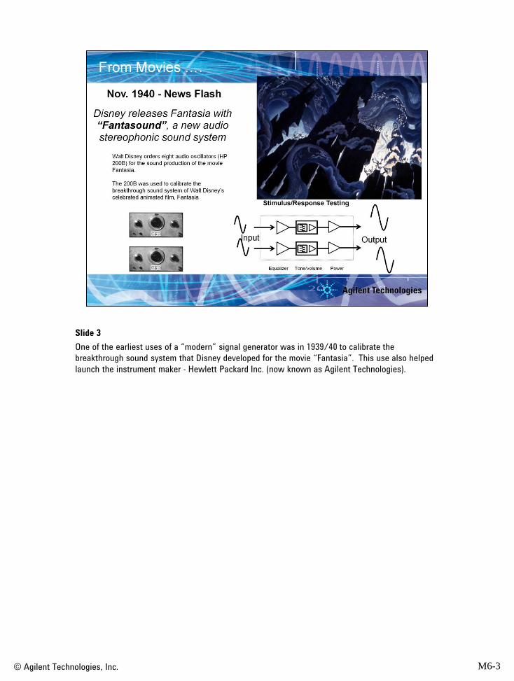
One of the earliest uses of a “modern” signal generator was in 1939/40 to calibrate the
breakthrough sound system that Disney developed for the movie “Fantasia”. This use also helped
launch the instrument maker - Hewlett Packard Inc. (now known as Agilent Technologies).

© Agilent Technologies, Inc. M6-4
Slide 4
Today’s use of signal generators includes the design, testing and maintenance of radar
transmitters and receivers. The signal generator’s functionality and performance is able to
simulate various blocks of the radar system.

© Agilent Technologies, Inc. M6-5
Slide 5
Even though communication devices have gone digital, the need to test the transmitters and
receivers remains, even as the requirements become more complex.
© Agilent Technologies, Inc M6-6
Slide 6
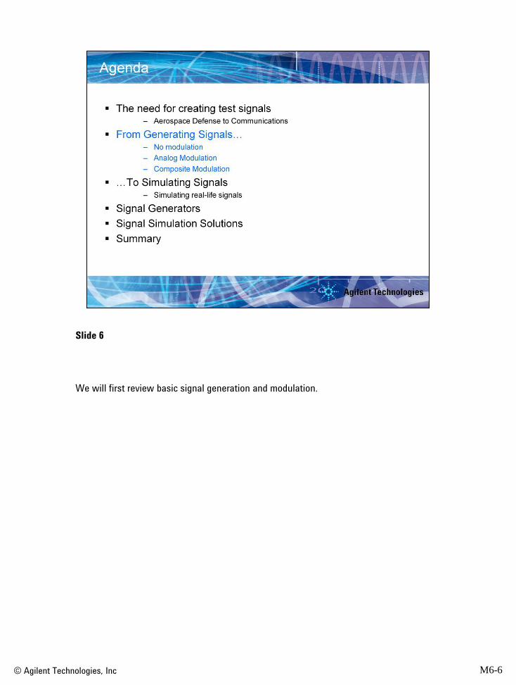
We will first review basic signal generation and modulation.

© Agilent Technologies, Inc M6-7
Slide 7
A basic signal with no modulation is that of a sine wave and is usually referred to as a continuous
wave (CW) signal. A basic signal source produces sine waves.
Ideally, the sine wave is perfect. In the frequency domain, it is viewed as a single line at some
specified frequency. Specifications tend to deal with deviations from this perfect sine wave in both
amplitude and frequency of the signal.
We generally refer to CW signals that are less than 6 GHz to be RF signals, those from 6 GHz to
less than 70 GHz to be microwave signals, and those greater than 70 GHz to millimeter signals.
© Agilent Technologies, Inc M6-8
Slide 8
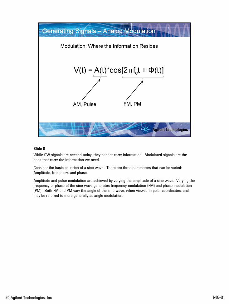
While CW signals are needed today, they cannot carry information. Modulated signals are the
ones that carry the information we need.
Consider the basic equation of a sine wave. There are three parameters that can be varied:
Amplitude, frequency, and phase.
Amplitude and pulse modulation are achieved by varying the amplitude of a sine wave. Varying the
frequency or phase of the sine wave generates frequency modulation (FM) and phase modulation
(PM). Both FM and PM vary the angle of the sine wave, when viewed in polar coordinates, and
may be referred to more generally as angle modulation.

© Agilent Technologies, Inc M6-9
Slide 9
In amplitude modulation, the modulating signal varies the amplitude of the carrier. The modulating signal carries the information. Amplitude modulation can be represented by this equation where fc is the carrier, fm is the modulation frequency and m is the depth of modulation, also referred to as the modulation index. The depth of modulation is defined as the ratio of the peak of the modulating signal to the peak of the carrier signal. When the depth of modulation is expressed as a percentage, the modulation is referred to as linear AM. When the depth of modulation is expressed in "dB", the modulation is referred to as logarithmic AM.
The spectrum of an AM signal contains several sidebands. These sidebands are created from the sum and difference of the carrier frequency and the modulation frequency.

© Agilent Technologies, Inc M6-10
Slide 10
AM signals are used in AM Radio, to emulate the radiation pattern of an antenna, and in early digital communications - transmitting 1s and 0s.
© Agilent Technologies, Inc M6-11
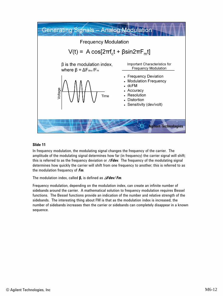
Slide 11
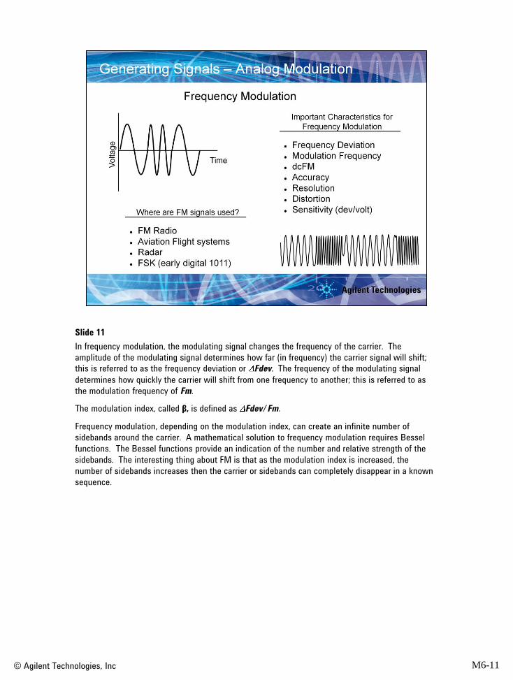
In frequency modulation, the modulating signal changes the frequency of the carrier. The
amplitude of the modulating signal determines how far (in frequency) the carrier signal will shift;
this is referred to as the frequency deviation or Fdev. The frequency of the modulating signal
determines how quickly the carrier will shift from one frequency to another; this is referred to as
the modulation frequency of Fm.
The modulation index, called β, is defined as Fdev/Fm.
Frequency modulation, depending on the modulation index, can create an infinite number of
sidebands around the carrier. A mathematical solution to frequency modulation requires Bessel
functions. The Bessel functions provide an indication of the number and relative strength of the
sidebands. The interesting thing about FM is that as the modulation index is increased, the
number of sidebands increases then the carrier or sidebands can completely disappear in a known
sequence.
© Agilent Technologies, Inc M6-12
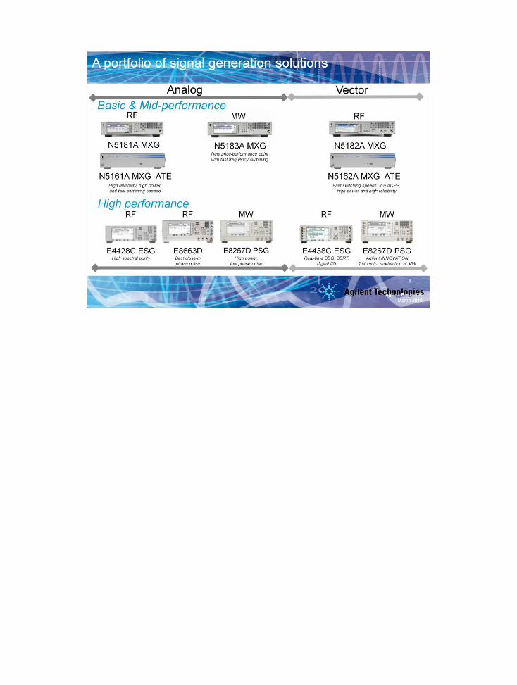
Slide 11
In frequency modulation, the modulating signal changes the frequency of the carrier. The
amplitude of the modulating signal determines how far (in frequency) the carrier signal will shift;
this is referred to as the frequency deviation or Fdev. The frequency of the modulating signal
determines how quickly the carrier will shift from one frequency to another; this is referred to as
the modulation frequency of Fm.
The modulation index, called β, is defined as Fdev/Fm.
Frequency modulation, depending on the modulation index, can create an infinite number of
sidebands around the carrier. A mathematical solution to frequency modulation requires Bessel
functions. The Bessel functions provide an indication of the number and relative strength of the
sidebands. The interesting thing about FM is that as the modulation index is increased, the
number of sidebands increases then the carrier or sidebands can completely disappear in a known
sequence.

© Agilent Technologies, Inc M6-13
Slide 13
Phase modulation is very similar to frequency modulation. The modulating signal causes the
phase of the carrier to shift. The amplitude of the modulating signal determines the phase
deviation. The modulation index, β, is defined as the phase deviation of the carrier. Notice that
the rate of the phase modulation does not enter into a calculation of β. The spectrum modulation
components are spaced as with FM and are determined by the rate of phase modulation, but β will
not change if the rate of phase modulation is varied. If β doesn't change, the shape of the
spectrum doesn't change: only the component spacing changes. This is really the only way of
differentiating analog FM from analog PM.

© Agilent Technologies, Inc M6-14
Slide 14
PM signals also have been used in early digital communication systems (transmitting 1’s and 0’s)
and in radars.
© Agilent Technologies, Inc M6-15
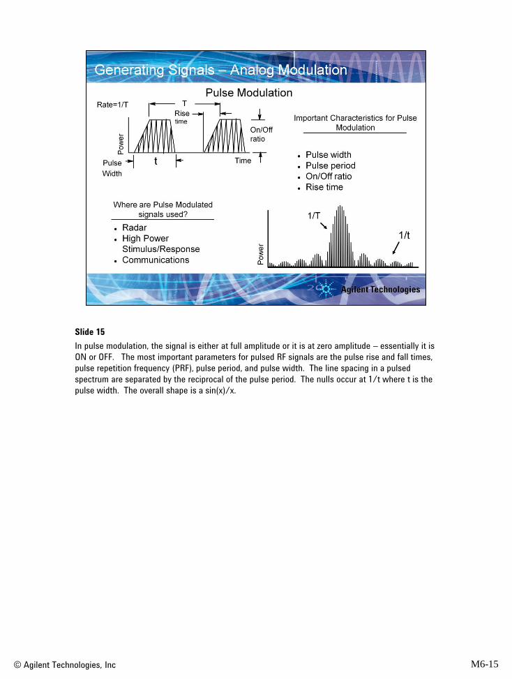
Slide 15
In pulse modulation, the signal is either at full amplitude or it is at zero amplitude – essentially it is
ON or OFF. The most important parameters for pulsed RF signals are the pulse rise and fall times,
pulse repetition frequency (PRF), pulse period, and pulse width. The line spacing in a pulsed
spectrum are separated by the reciprocal of the pulse period. The nulls occur at 1/t where t is the
pulse width. The overall shape is a sin(x)/x.

© Agilent Technologies, Inc M6-16
Slide 16
Pulse modulation is important in both communications and radar applications. In communications,
the baseband modulation signal is essentially a pulse and the upconverted signal may be time
multiplexed (turned on and off rapidly).
© Agilent Technologies, Inc M6-17
Slide 17
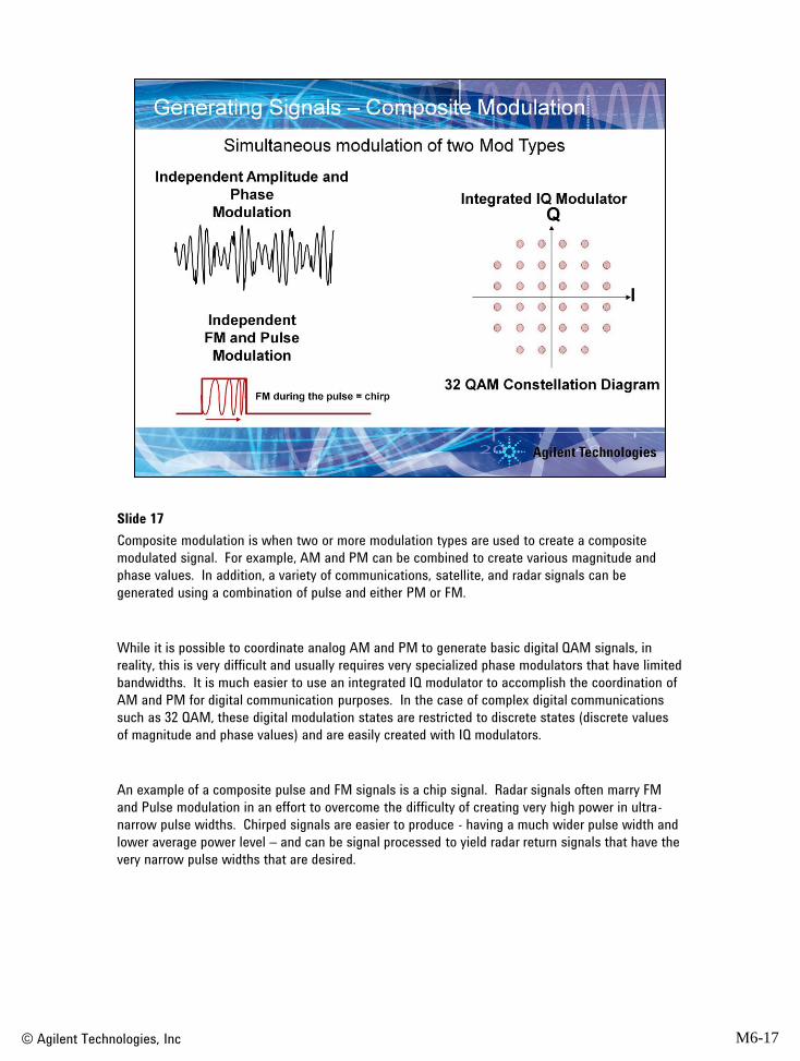
Composite modulation is when two or more modulation types are used to create a composite
modulated signal. For example, AM and PM can be combined to create various magnitude and
phase values. In addition, a variety of communications, satellite, and radar signals can be
generated using a combination of pulse and either PM or FM.
While it is possible to coordinate analog AM and PM to generate basic digital QAM signals, in
reality, this is very difficult and usually requires very specialized phase modulators that have limited
bandwidths. It is much easier to use an integrated IQ modulator to accomplish the coordination of
AM and PM for digital communication purposes. In the case of complex digital communications
such as 32 QAM, these digital modulation states are restricted to discrete states (discrete values
of magnitude and phase values) and are easily created with IQ modulators.
An example of a composite pulse and FM signals is a chip signal. Radar signals often marry FM
and Pulse modulation in an effort to overcome the difficulty of creating very high power in ultra-
narrow pulse widths. Chirped signals are easier to produce - having a much wider pulse width and
lower average power level – and can be signal processed to yield radar return signals that have the
very narrow pulse widths that are desired.

© Agilent Technologies, Inc M6-18
Slide 18
Let’s take a look at the composite modulation of magnitude (amplitude) and phase. The phasor
(vector) notation provides a convenient way of measuring how the sine wave is changing over time
and the display of a vector is commonly referred to as a polar display.
When displaying a modulated signal, the carrier is used as the reference signal for any modulation
and so a phase of 0 degrees is selected as having no modulation. The rotation of the phasor is
referenced to the carrier frequency, therefore the phasor will only rotate if its frequency (or phase)
is different from that of the carrier.
© Agilent Technologies, Inc M6-19
Slide 19
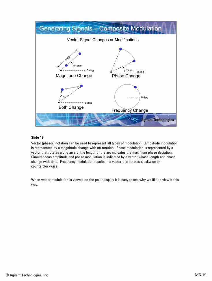
Vector (phasor) notation can be used to represent all types of modulation. Amplitude modulation
is represented by a magnitude change with no rotation. Phase modulation is represented by a
vector that rotates along an arc; the length of the arc indicates the maximum phase deviation.
Simultaneous amplitude and phase modulation is indicated by a vector whose length and phase
change with time. Frequency modulation results in a vector that rotates clockwise or
counterclockwise.
When vector modulation is viewed on the polar display it is easy to see why we like to view it this
way.

© Agilent Technologies, Inc M6-20
Slide 20
When we describe the vectors in digital modulation, we typically don’t use magnitude and phase
values. The polar plane can very easily be mapped to a rectangular format (with horizontal and
vertical axis) called the I-Q plane: I (In-phase) and Q (Quadrature). The I axis lies on the zero
degree phase reference, and the Q axis is rotated by 90 degrees. The signal vector’s projection
onto the I axis is the “I” component and the projection onto the Q axis is its “Q” component.
I/Q diagrams are particularly useful because they mirror the way most digital communications
signals are created using an I/Q modulator. Independent DC voltages (I and Q components)
provided to the input of an I/Q modulator correlate to a composite signal with a specific amplitude
and phase at the modulator output. Conversely, the amplitude and phase of a modulated signal
sent to an I/Q demodulator, will correspond to discrete DC values at the demodulator’s output.
© Agilent Technologies, Inc M6-21
Slide 21
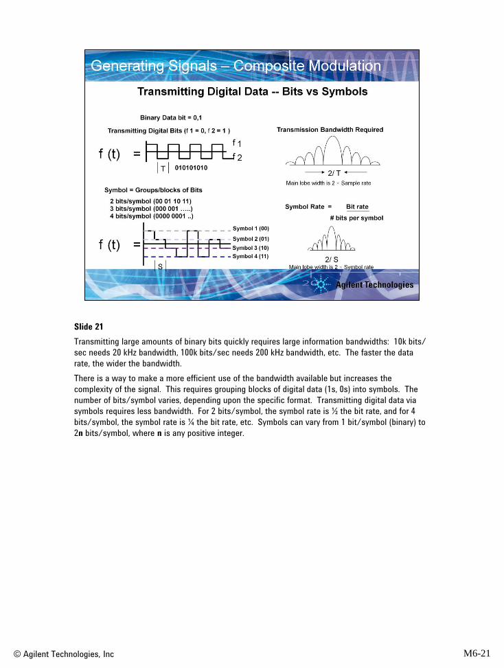
Transmitting large amounts of binary bits quickly requires large information bandwidths: 10k bits/
sec needs 20 kHz bandwidth, 100k bits/sec needs 200 kHz bandwidth, etc. The faster the data
rate, the wider the bandwidth.
There is a way to make a more efficient use of the bandwidth available but increases the
complexity of the signal. This requires grouping blocks of digital data (1s, 0s) into symbols. The
number of bits/symbol varies, depending upon the specific format. Transmitting digital data via
symbols requires less bandwidth. For 2 bits/symbol, the symbol rate is ½ the bit rate, and for 4
bits/symbol, the symbol rate is ¼ the bit rate, etc. Symbols can vary from 1 bit/symbol (binary) to
2n bits/symbol, where n is any positive integer.
© Agilent Technologies, Inc M6-22
Slide 22
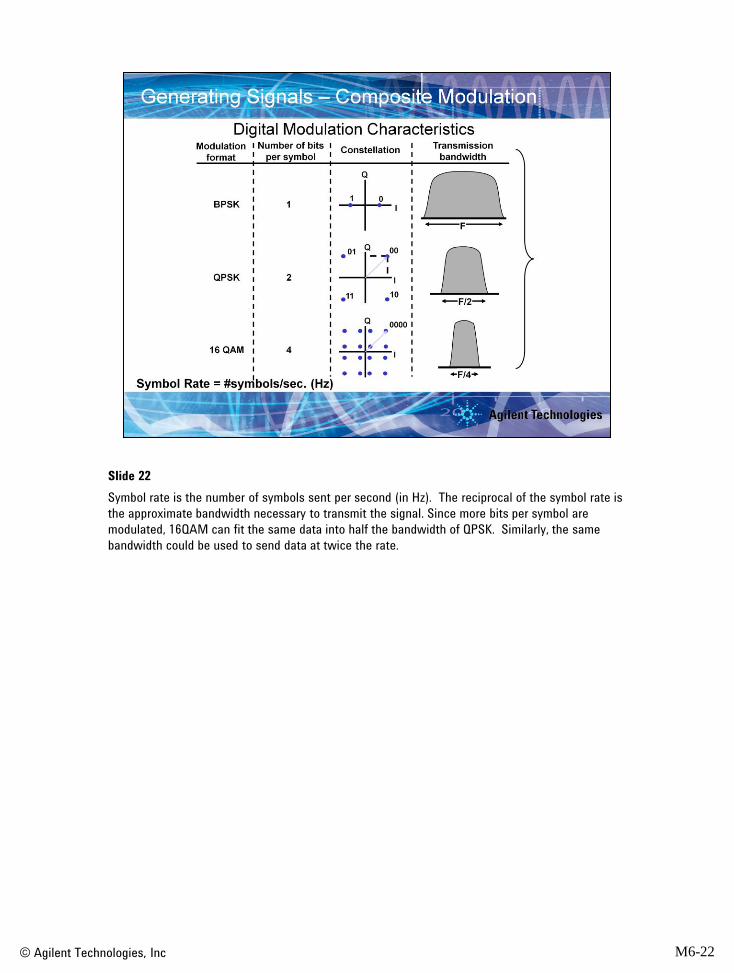
Symbol rate is the number of symbols sent per second (in Hz). The reciprocal of the symbol rate is
the approximate bandwidth necessary to transmit the signal. Since more bits per symbol are
modulated, 16QAM can fit the same data into half the bandwidth of QPSK. Similarly, the same
bandwidth could be used to send data at twice the rate.
© Agilent Technologies, Inc M6-23
Slide 23
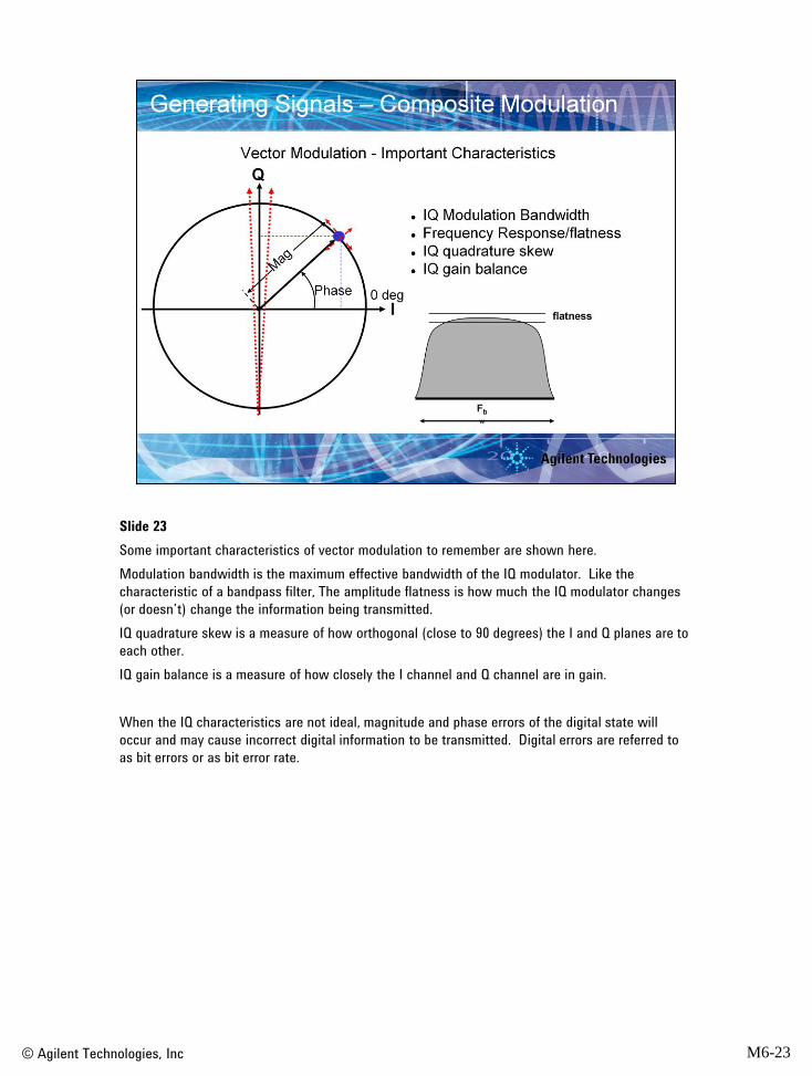
Some important characteristics of vector modulation to remember are shown here.
Modulation bandwidth is the maximum effective bandwidth of the IQ modulator. Like the
characteristic of a bandpass filter, The amplitude flatness is how much the IQ modulator changes
(or doesn’t) change the information being transmitted.
IQ quadrature skew is a measure of how orthogonal (close to 90 degrees) the I and Q planes are to
each other.
IQ gain balance is a measure of how closely the I channel and Q channel are in gain.
When the IQ characteristics are not ideal, magnitude and phase errors of the digital state will
occur and may cause incorrect digital information to be transmitted. Digital errors are referred to
as bit errors or as bit error rate.

© Agilent Technologies, Inc M6-24
Slide 24
The most common use of IQ or vector modulation is in modern digital communications. Because
of the large modulation bandwidths and the ease of creating composite modulated signals, it is
also used in modern radar systems.

© Agilent Technologies, Inc M6-25
Slide 25
Now we are going to explore signal simulation.
© Agilent Technologies, Inc M6-26
Slide 26
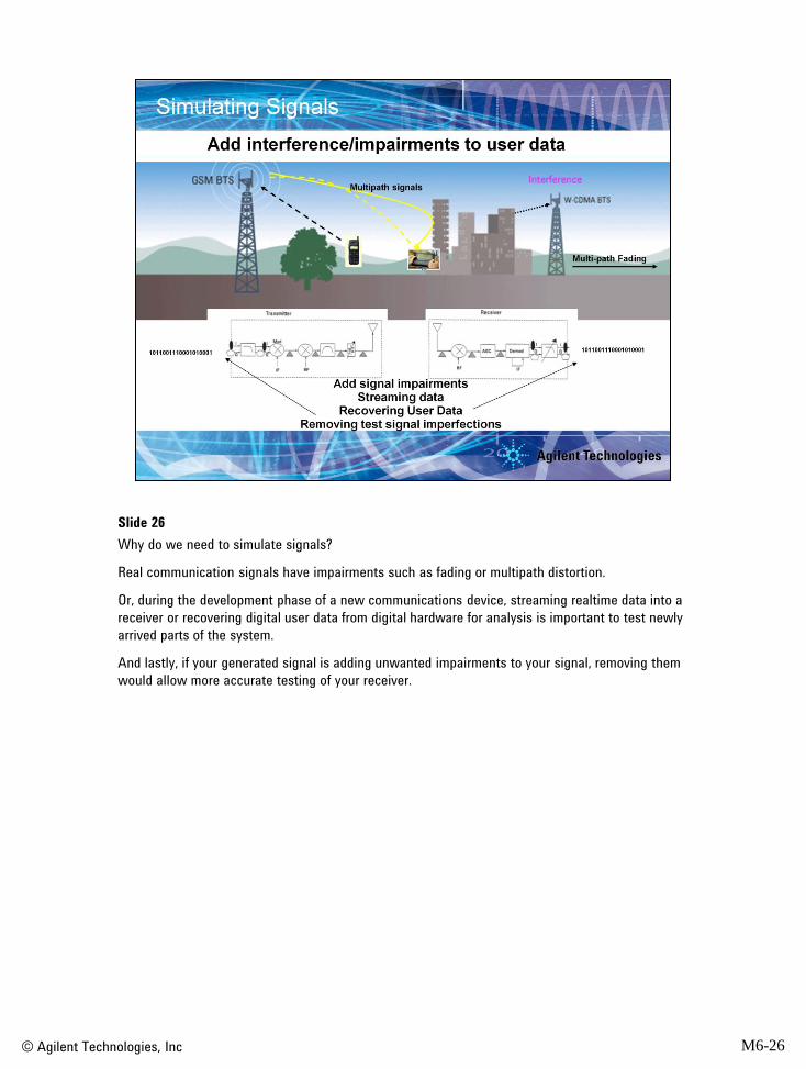
Why do we need to simulate signals?
Real communication signals have impairments such as fading or multipath distortion.
Or, during the development phase of a new communications device, streaming realtime data into a
receiver or recovering digital user data from digital hardware for analysis is important to test newly
arrived parts of the system.
And lastly, if your generated signal is adding unwanted impairments to your signal, removing them
would allow more accurate testing of your receiver.
© Agilent Technologies, Inc M6-27
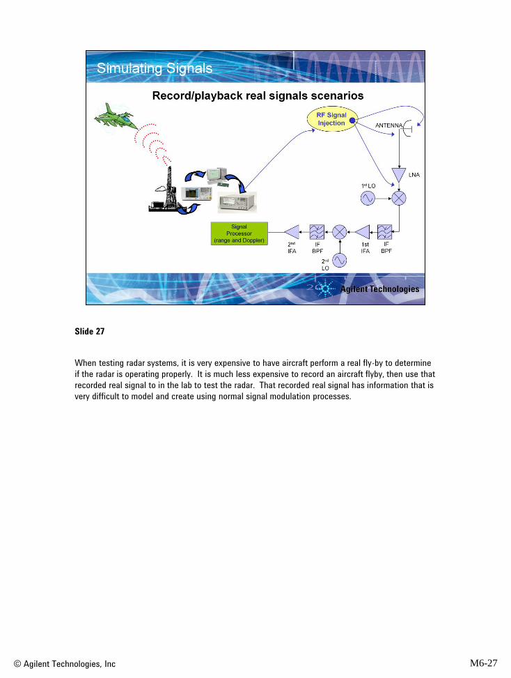
Slide 27
When testing radar systems, it is very expensive to have aircraft perform a real fly-by to determine
if the radar is operating properly. It is much less expensive to record an aircraft flyby, then use that
recorded real signal to in the lab to test the radar. That recorded real signal has information that is
very difficult to model and create using normal signal modulation processes.

© Agilent Technologies, Inc M6-28
Slide 28
Now we are going to examine signal generator block diagrams, specifications,
applications.

© Agilent Technologies, Inc M6-29
Slide 29
This is a list of general categories for different types of signals. A signal generator’s capabilities
increase as you progress from cw to analog and vector signals.

© Agilent Technologies, Inc M6-30
Slide 30
The above block diagram provides greater detail for an RF CW source.
The reference section’s reference oscillator determines the accuracy of the Source’s output frequency. The important characteristics are the short term stability (phase noise) and the long term stability (or the aging rate). The reference section supplies a sine wave with a known frequency to phase-locked loop (PLL) in the synthesizer section.
The synthesizer section is responsible for producing a sine wave at the desired frequency. The VCO (voltage controlled oscillator) produces the less accurate sine wave. The PLL maintains the output frequency at the desired setting which translates the frequency accuracy of the reference oscillator to the output of the VCO.
The synthesizer section supplies a stable frequency to the output section. The output section determines the overall amplitude range and accuracy of the source. Amplitude range is determined by the available amplification and attenuation. Amplitude accuracy, or level accuracy, is maintained by monitoring the output power and continuously adjusting the power as needed.
Let's take a look at each section in more detail.

© Agilent Technologies, Inc M6-31
Slide 31
The heart of the reference section is the reference oscillator. The reference oscillator must be
inexpensive, extremely stable and adjustable over a narrow range of frequencies. A stable
reference oscillator will ensure that the frequency output of the source remains accurate in
between calibrations. By comparing the reference oscillator to a frequency standard, such as a
Cesium oscillator, and adjusting as needed, the source can be calibrated with an output that is
traceable.
Of all materials today, crystalline quartz best meets these criteria. The fundamental frequency of
quartz is affected by several parameters: aging, temperature, and line voltage. Over time, the
stress placed on a quartz crystal will affect the oscillation frequency. Temperature changes cause
changes in the crystal structure which affect the oscillation frequency. The piezoelectric nature of
quartz is also affected by the electric fields created inside the source by the line voltage.
To improve the performance of quartz, temperature compensation circuitry is used to limit the
variations in output frequency that result from variations in the operating temperature. Crystals
with such compensation are referred to as Temperature Compensated crystal oscillators or
TCXO's. OCXO's are crystals that have been placed in an Oven Controlled environment. This
environment maintains a constant temperature and provides shielding from the effects of line
voltage. The stability for both TCXO's and OCXO's is tabulated above.
Many sources also provide an external input that may be used to lock the oscillator to an external
or house reference. The source, however, does not require an external reference.

© Agilent Technologies, Inc M6-32
Slide 32
In the synthesizer, a VCO produces an output frequency for an input voltage. A simple VCO can be constructed from a varactor, a voltage-variable capacitor commonly made from a reverse-biased pn junction diode. The capacitance across the diode decreases as the reverse bias to the diode increases. When placed in an oscillator circuit, the tunable capacitor enables the output oscillation to be tuned. This output is inherently unstable so a PLL is required to maintain frequency stability.
Most of the VCO output is sent to the output section of the source. A portion of the VCO output is divided to a lower frequency and compared to the signal supplied by the reference section using the phase detector. The output of the phase detector will be a dc offset with an error signal. The dc offset represents the constant phase difference between the 5 MHz signal from the reference and the 5 MHz signal from the Frac-N divide circuit. The error signal represents unwanted frequency drift. The output of the phase detector is filtered and amplified to properly drive the VCO. If the VCO does not drift, there will be (almost) no error signal at the output of the phase detector and the control voltage to the VCO will not change. If the VCO drifts upwards (or downwards), the error signal at the output of the phase detector will adjust the VCO output downwards (or upwards) to maintain a stable frequency output.
© Agilent Technologies, Inc M6-33
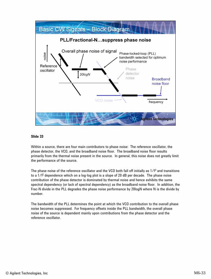
Slide 33
Within a source, there are four main contributors to phase noise: The reference oscillator, the
phase detector, the VCO, and the broadband noise floor. The broadband noise floor results
primarily from the thermal noise present in the source. In general, this noise does not greatly limit
the performance of the source.
The phase noise of the reference oscillator and the VCO both fall off initially as 1/f3 and transitions
to a 1/f2 dependence which on a log-log plot is a slope of 20 dB per decade. The phase noise
contribution of the phase detector is dominated by thermal noise and hence exhibits the same
spectral dependency (or lack of spectral dependency) as the broadband noise floor. In addition, the
Frac-N divide in the PLL degrades the phase noise performance by 20logN where N is the divide by
number.
The bandwidth of the PLL determines the point at which the VCO contribution to the overall phase
noise becomes suppressed. For frequency offsets inside the PLL bandwidth, the overall phase
noise of the source is dependent mainly upon contributions from the phase detector and the
reference oscillator.

© Agilent Technologies, Inc M6-34
Slide 34
The output section maintains amplitude or level accuracy by measuring the output power and compensating for deviations from the set power level. The ALC driver digitizes the detector output and compares the digitized signal to a look-up table to provide the appropriate modulator drive such that the detected power becomes equivalent to the desired power. Frequently, external losses from cabling and switching between the output of the signal source and the device under test (DUT) attenuate the signal. Another look-up table that compensates for external losses can be input to extend the automatic leveling to the input of the DUT.
With no output attenuation applied, the source amplitude is at a maximum determined by the power amp and the loss between the output of the amp and the output connector. The main source of loss is the output attenuator. The output attenuator will introduce a finite amount of loss even when the attenuation is set to 0 dB. The purpose of the output attenuator is to reduce the output power in a calibrated and repeatable fashion. Today attenuators are available that provide output ranges from +23 dBm (no attenuation applied to the source) to -127 dBm (maximum attenuation applied). There are two types of attenuators that are commonly used: mechanical and solid state.
Mechanical attenuators introduce very little loss between the output of the power amp and the output connector. Thus a high output power can be achieved without over-driving the output amplifier. Operating at low drive levels reduces the level of harmonics generated by the source. Mechanical attenuators do, however, have finite lifetimes. A typical mechanical attenuator will live for five million cycles. For an ATE application in which the power level is changed every two seconds, the attenuator will fail after about a year.

© Agilent Technologies, Inc M6-35
Slide 35
The block diagram of a microwave CW source is similar to that of an RF CW source; each has the
same three basic sections. There are differences, however. Although the reference section only
has one reference oscillator, two signals are supplied to the synthesizer section from the reference
section.
The output frequency of the synthesizer section is generated from a Yttrium-iron-garnet (YIG)
oscillator which is tuned with a magnetic field. The feedback mechanism that ensures frequency
stability is a phase locked loop; however, in addition to the fractional-N divide, harmonic sampling
is used to divide the output frequency.

© Agilent Technologies, Inc M6-36
Slide 36
Understanding source specifications is critical when determining the appropriate source for an
application. For CW sources, the specifications are generally divided into three broad categories:
Frequency, amplitude (or output), and spectral purity.
Range, resolution, and accuracy are the main frequency specifications. Range specifies the range
of output frequencies that the source can produce. Resolution is the smallest frequency
increment. The accuracy of a source is affected by two parameters: The stability of the reference
oscillator and the amount of time that has passed since the source was last calibrated.
A typical (but very good) reference oscillator may have an aging rate of 0.152ppm (parts-per-
million) per year. The aging rate indicates how far the reference will drift (either up or down) from
its specified value. At 1 GHz, a source that has not been calibrated for one year with an aging rate
of 0.152ppm per year will be within 152 Hz of its specified output frequency.

© Agilent Technologies, Inc M6-37
Slide 37
Range, accuracy, resolution, switching speed, and reverse power protection are the main amplitude
specifications. The range of a source is determined by the maximum output power and the
amount of internal attenuation built into the source. The resolution of a source indicates the
smallest amplitude increment. Switching speed is a measure of how fast the source can change
from one amplitude level to another.
Sources are often used to test transceivers. Because transceivers have transmitters, the
connection between a source and the transceiver could conduct a signal from the device being
tested to the output connector of the source. Reverse power protection prevents transmitter
signals from damaging the source.
© Agilent Technologies, Inc M6-38
Slide 38
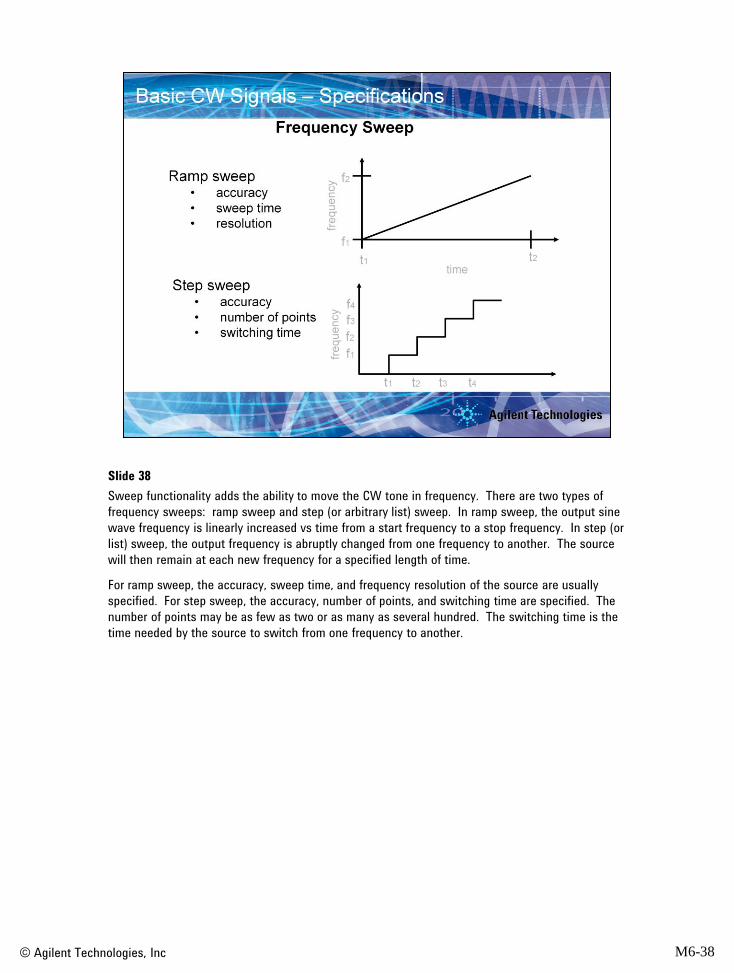
Sweep functionality adds the ability to move the CW tone in frequency. There are two types of
frequency sweeps: ramp sweep and step (or arbitrary list) sweep. In ramp sweep, the output sine
wave frequency is linearly increased vs time from a start frequency to a stop frequency. In step (or
list) sweep, the output frequency is abruptly changed from one frequency to another. The source
will then remain at each new frequency for a specified length of time.
For ramp sweep, the accuracy, sweep time, and frequency resolution of the source are usually
specified. For step sweep, the accuracy, number of points, and switching time are specified. The
number of points may be as few as two or as many as several hundred. The switching time is the
time needed by the source to switch from one frequency to another.

© Agilent Technologies, Inc M6-39
Slide 39
Amplitude specifications also impacts the sweeping capability of the CW source. In a frequency
sweep, the output power will vary by no more than the flatness specification throughout the
sweep. In addition, the output power is also constrained to remain within the level accuracy
specification of the source. For example, consider a source with a level accuracy of +/- 1.0 dB and
a flatness specification of +/- 0.7 dB. If the output is set to 0 dBm, the actual output could really
be as high a 1 dBm or as low as -1 dBm. If the actual output is 1 dBm, during the sweep, the
power can only drift downward by the 0.7 dB, the flatness specification; the power cannot drift
above 1 dBm because the ALC will constrain the power to remain within 1 dB of the set level of 0
dBm.
CW sources can also sweep its power level in addition to their frequency. When sweeping power,
the sweep range will determine possible range of output powers. The slope range will determine
how quickly the source can sweep from one power to another. In place of a power slope, some
sources allow the user to specify the number of points in the power sweep and the dwell time.
Source match is generally specified in standing wave ratio (SWR) which is really just a measure of
how close the source output is to 50 ohms. The value of SWR can range between one and infinity.
Some of the power from a source with a SWR greater than one, when connected to a 50 ohm load,
will be reflected back to the source which sets up the standing waves.
© Agilent Technologies, Inc M6-40
Slide 40
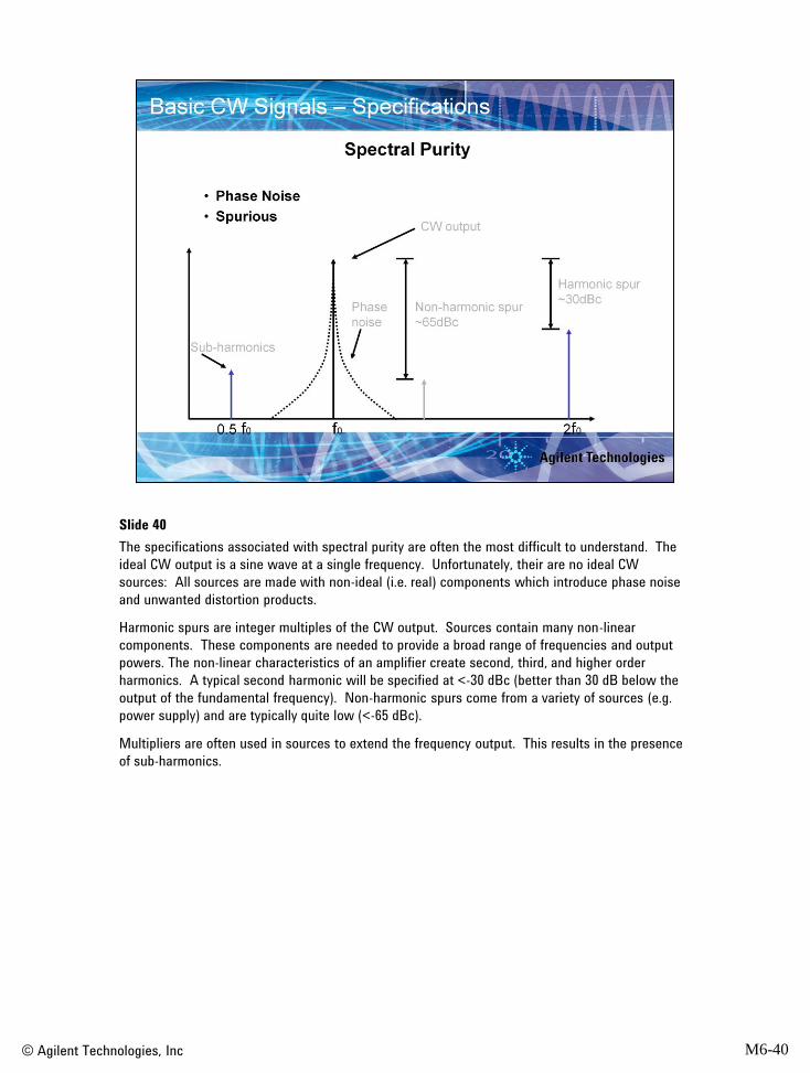
The specifications associated with spectral purity are often the most difficult to understand. The
ideal CW output is a sine wave at a single frequency. Unfortunately, their are no ideal CW
sources: All sources are made with non-ideal (i.e. real) components which introduce phase noise
and unwanted distortion products.
Harmonic spurs are integer multiples of the CW output. Sources contain many non-linear
components. These components are needed to provide a broad range of frequencies and output
powers. The non-linear characteristics of an amplifier create second, third, and higher order
harmonics. A typical second harmonic will be specified at <-30 dBc (better than 30 dB below the
output of the fundamental frequency). Non-harmonic spurs come from a variety of sources (e.g.
power supply) and are typically quite low (<-65 dBc).
Multipliers are often used in sources to extend the frequency output. This results in the presence
of sub-harmonics.
© Agilent Technologies, Inc M6-41
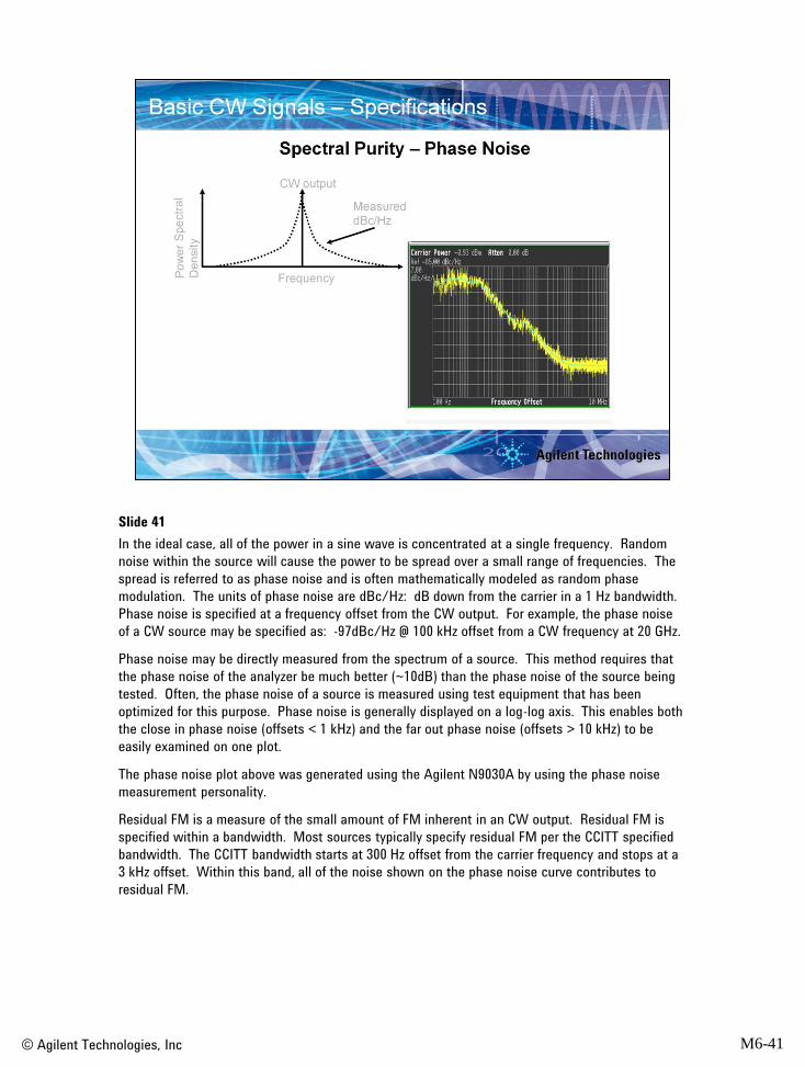
Slide 41
In the ideal case, all of the power in a sine wave is concentrated at a single frequency. Random
noise within the source will cause the power to be spread over a small range of frequencies. The
spread is referred to as phase noise and is often mathematically modeled as random phase
modulation. The units of phase noise are dBc/Hz: dB down from the carrier in a 1 Hz bandwidth.
Phase noise is specified at a frequency offset from the CW output. For example, the phase noise
of a CW source may be specified as: -97dBc/Hz @ 100 kHz offset from a CW frequency at 20 GHz.
Phase noise may be directly measured from the spectrum of a source. This method requires that
the phase noise of the analyzer be much better (~10dB) than the phase noise of the source being
tested. Often, the phase noise of a source is measured using test equipment that has been
optimized for this purpose. Phase noise is generally displayed on a log-log axis. This enables both
the close in phase noise (offsets < 1 kHz) and the far out phase noise (offsets > 10 kHz) to be
easily examined on one plot.
The phase noise plot above was generated using the Agilent N9030A by using the phase noise
measurement personality.
Residual FM is a measure of the small amount of FM inherent in an CW output. Residual FM is
specified within a bandwidth. Most sources typically specify residual FM per the CCITT specified
bandwidth. The CCITT bandwidth starts at 300 Hz offset from the carrier frequency and stops at a
3 kHz offset. Within this band, all of the noise shown on the phase noise curve contributes to
residual FM.
© Agilent Technologies, Inc M6-42
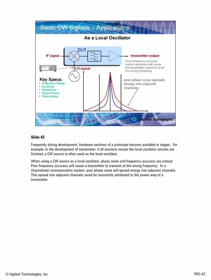
Slide 42
Frequently during development, hardware sections of a prototype become available in stages. For
example, in the development of transmitter, if all sections except the local oscillator section are
finished, a CW source is often used as the local oscillator.
When using a CW source as a local oscillator, phase noise and frequency accuracy are critical.
Poor frequency accuracy will cause a transmitter to transmit at the wrong frequency. In a
channelized communication system, poor phase noise will spread energy into adjacent channels.
This spread into adjacent channels could be incorrectly attributed to the power amp of a
transmitter.
© Agilent Technologies, Inc M6-43
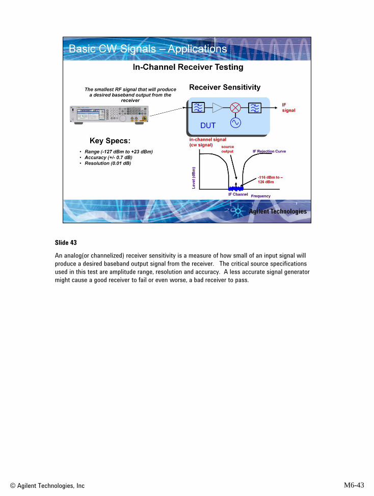
Slide 43
An analog(or channelized) receiver sensitivity is a measure of how small of an input signal will
produce a desired baseband output signal from the receiver. The critical source specifications
used in this test are amplitude range, resolution and accuracy. A less accurate signal generator
might cause a good receiver to fail or even worse, a bad receiver to pass.
© Agilent Technologies, Inc M6-44
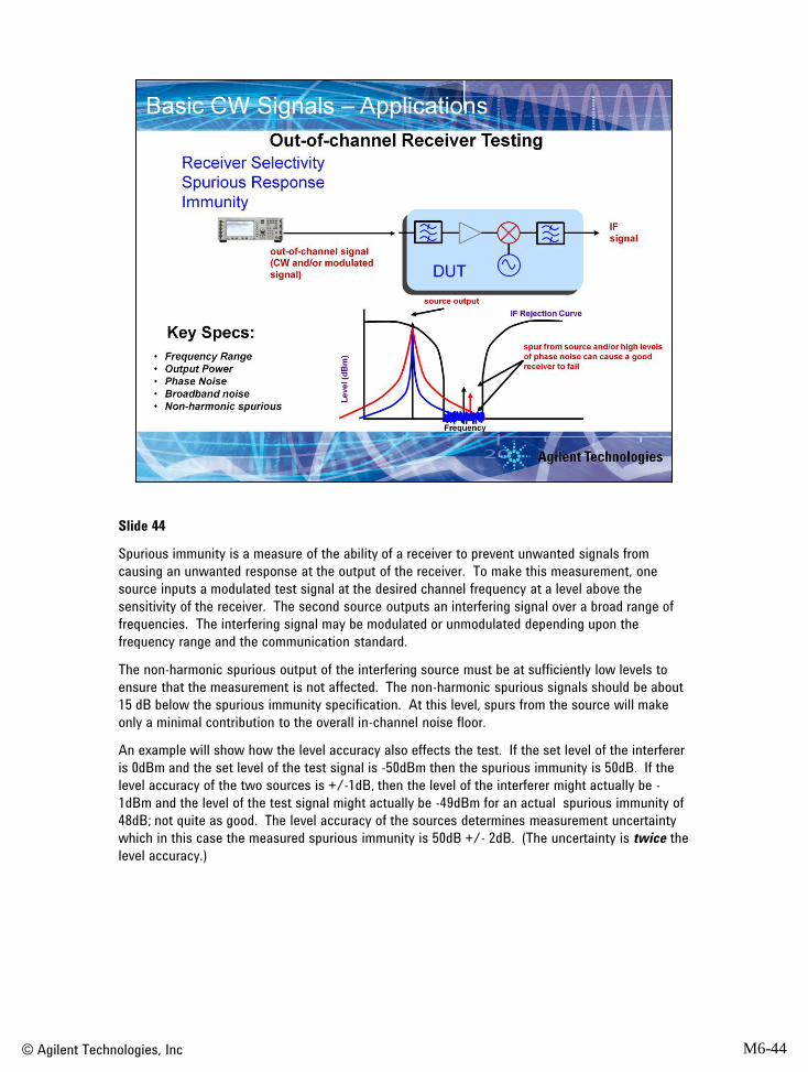
Slide 44
Spurious immunity is a measure of the ability of a receiver to prevent unwanted signals from
causing an unwanted response at the output of the receiver. To make this measurement, one
source inputs a modulated test signal at the desired channel frequency at a level above the
sensitivity of the receiver. The second source outputs an interfering signal over a broad range of
frequencies. The interfering signal may be modulated or unmodulated depending upon the
frequency range and the communication standard.
The non-harmonic spurious output of the interfering source must be at sufficiently low levels to
ensure that the measurement is not affected. The non-harmonic spurious signals should be about
15 dB below the spurious immunity specification. At this level, spurs from the source will make
only a minimal contribution to the overall in-channel noise floor.
An example will show how the level accuracy also effects the test. If the set level of the interferer
is 0dBm and the set level of the test signal is -50dBm then the spurious immunity is 50dB. If the
level accuracy of the two sources is +/-1dB, then the level of the interferer might actually be -
1dBm and the level of the test signal might actually be -49dBm for an actual spurious immunity of
48dB; not quite as good. The level accuracy of the sources determines measurement uncertainty
which in this case the measured spurious immunity is 50dB +/- 2dB. (The uncertainty is twice the
level accuracy.)
© Agilent Technologies, Inc M6-45
Slide 45
Third order intercept, or TOI, is a common amplifier measurement made by using two CW sources
which are combined at the input of an amplifier (DUT). The frequencies of each source are slightly
offset from each other and yet still inside the bandwidth of the amplifier. The non-linearities of an
amplifier will produce third order mixing products: fL = 2f1 - f2 and fU = 2f2 - f1 where f1 and f2 are
the output frequencies of the two sources.
Spurious signals from the CW sources can corrupt the measurement. When selecting an
appropriate source, the non-harmonic spurious levels should be well below the third order products
produced by the amplifier under test.
The test system can also introduce sources of error. Whenever two signals are input to a
combiner, the non-linearities of the sources will create intermodulation products. The
intermodulation products, when using a simple combiner, are created by the ALC of the source.
The signal from the first source passes through the resistive combiner network and into the
second source output with a 6 dB loss and the loss associated with the output attenuation of the
second source. Because the two sources are at different frequencies, the sum of the two signals
has an AM component equal to the difference frequency. For difference frequencies that are
within the bandwidth of the ALC, the ALC of the second source sees this additional power and
tries to level the output by adding AM. The intermodulation products created by the test system
are at the same frequencies as those created by the amplifier under test.
Intermodulation products can be reduced either through better isolation of the signal sources or by
suppressing the power that transfers from one source to the other wit a circulator.
© Agilent Technologies, Inc M6-46
Slide 46
Similar to IMD testing of amplifiers, IMD testing of receivers is testing the IMD immunity of the
entire receiver. The same source specifications are important.

© Agilent Technologies, Inc M6-47
Slide 47
The major application of sweeping CW generators is stimulus-response testing, or to find the
swept response of the DUT. Frequency sweeps are done to determine the frequency response of
devices. Power sweeps, typically done on amplifiers, measure linearity and saturation levels.
When measuring the frequency response of a device, the following sweeper specifications are
important:
Specification Effect
Frequency Accuracy center frequency and bandwidth of the device under test
(DUT)
Output Power (Level) gain or loss
Flatness flatness
Speed test cost
residual FM ability to test high Q devices
Frequency response measurements are made on many types of devices including amplifiers, filters,
and mixers. For a more detailed explanation of these types of measurements, see the Network
Analysis Back to Basics paper.
© Agilent Technologies, Inc M6-48
Slide 48
Now we are going to examine the effect of adding analog modulation to the basic generator.

© Agilent Technologies, Inc M6-49
Slide 49
The block diagram of an analog signal generator does not differ greatly from that of a CW
generator. Instead of altering the blocks of the source, there are additional components that allow
the source to modulate the carrier.
The FM and PM inputs are to the frequency control block of the synthesizer in order to modulate
the carrier. To change the frequency or phase of the signal generator, this FM or PM input signal
is applied to the VCO. This signal, in addition to the reference oscillator signal, creates the FM or
PM signal.
To create AM, the AM signal needs to be applied to the ALC driver block. The ALC driver will
convert the voltages from the AM input into amplitude changes in the carrier through the ALC
modulator.
To create pulse modulation, a pulse input is added and that signal is applied to a pulse modulator,
which is in the output path of the signal.

© Agilent Technologies, Inc M6-50
Slide 50
In addition to the AM, FM, PM and pulse modulation capability being added to the CW source, an
internal modulation generator can also be added. Having an internal modulation generator
provides convenience and simplifies test setups.

© Agilent Technologies, Inc M6-51
Slide 51
Harmonic distortion testing requires an in-channel modulated signal. Any harmonics related to the
modulation signal in the baseband output may indicate a bad receiver. Since any distortion of the
input modulated signal will reflect in the output measurement, it is critical to have a modulated
signal that has low distortion. The example given here shows that for a receiver specification of
5% distortion and a 10 dB test margin requirement on the signal generator, the signal generator
must have lower than 1.58% modulation distortion for its modulated output signal.
© Agilent Technologies, Inc M6-52
Slide 52
When creating a composite modulation signal such as a chirped pulse, the key signal generator modulation specifications are FM deviation and rate, pulse rate, pulse width and pulse rise time.

© Agilent Technologies, Inc M6-53
Slide 53
Now we are going to examine the effect of adding vector modulation to the generator.
© Agilent Technologies, Inc M6-54
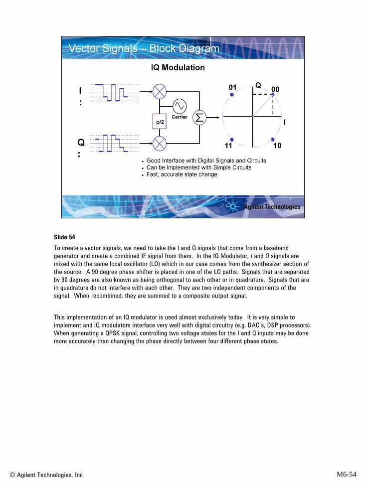
Slide 54
To create a vector signals, we need to take the I and Q signals that come from a baseband
generator and create a combined IF signal from them. In the IQ Modulator, I and Q signals are
mixed with the same local oscillator (LO) which in our case comes from the synthesizer section of
the source. A 90 degree phase shifter is placed in one of the LO paths. Signals that are separated
by 90 degrees are also known as being orthogonal to each other or in quadrature. Signals that are
in quadrature do not interfere with each other. They are two independent components of the
signal. When recombined, they are summed to a composite output signal.
This implementation of an IQ modulator is used almost exclusively today. It is very simple to
implement and IQ modulators interface very well with digital circuitry (e.g. DAC’s, DSP processors).
When generating a QPSK signal, controlling two voltage states for the I and Q inputs may be done
more accurately than changing the phase directly between four different phase states.

© Agilent Technologies, Inc M6-55
Slide 55
A vector signal generator is created by adding an IQ modulator to the basic CW block diagram of a
signal generator. In this configuration, the generation of the I and Q signals are done externally to
the vector signal generator.
© Agilent Technologies, Inc M6-56
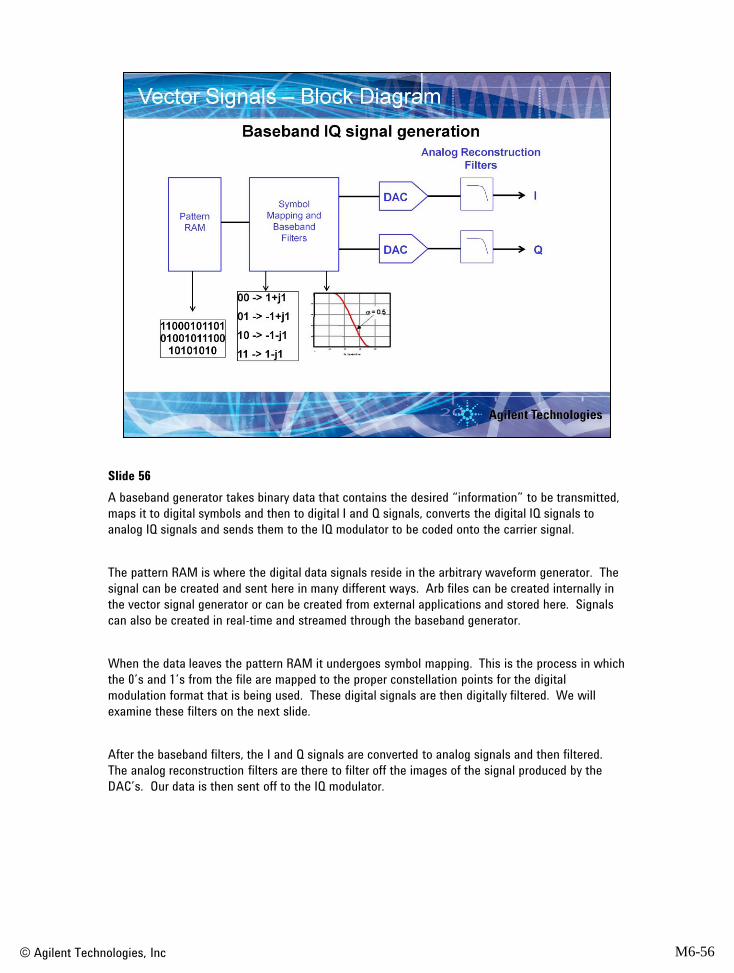
Slide 56
A baseband generator takes binary data that contains the desired “information” to be transmitted,
maps it to digital symbols and then to digital I and Q signals, converts the digital IQ signals to
analog IQ signals and sends them to the IQ modulator to be coded onto the carrier signal.
The pattern RAM is where the digital data signals reside in the arbitrary waveform generator. The
signal can be created and sent here in many different ways. Arb files can be created internally in
the vector signal generator or can be created from external applications and stored here. Signals
can also be created in real-time and streamed through the baseband generator.
When the data leaves the pattern RAM it undergoes symbol mapping. This is the process in which
the 0’s and 1’s from the file are mapped to the proper constellation points for the digital
modulation format that is being used. These digital signals are then digitally filtered. We will
examine these filters on the next slide.
After the baseband filters, the I and Q signals are converted to analog signals and then filtered.
The analog reconstruction filters are there to filter off the images of the signal produced by the
DAC’s. Our data is then sent off to the IQ modulator.
© Agilent Technologies, Inc M6-57
Slide 57
In the baseband generator there are 2 sets of filters. These filters are sometimes confused with
one another and so let’s take a brief look at the baseband filters. After the symbol mapping but
before the DAC’s is a set of filters called the baseband filters. These filters reside here mainly to
limit the bandwidth of the I and Q symbols. If no filters were placed in the path, the bandwidth of
the symbols would be theoretically infinite. However, most of the relevant information can be had
from the main lobe of the signal so we filter the signal to limit it’s bandwidth. Limiting the BW in
the frequency domain also smooths the transitions in the time domain, as can be seen in the slide.
The baseband filters can be many types and have different attributes that must be set in a signal
generator. You must first select the filter type. Common filter types are Root Raised Cosine,
Gaussian, and Rectangular. Next you must select the filter Alpha. This determines the sharpness
of the filter slope. For a "brick-wall" filter, alpha=0, and the estimated occupied bandwidth
= symbol rate. A filter this sharp is not realizable in the physical world and will ring
excessively. More common filters will range in alpha from .1 to .5.

© Agilent Technologies, Inc M6-58
Slide 58
For convenience, the I and Q signals can be generated by internally adding the baseband IQ
generator to the signal generator.
© Agilent Technologies, Inc M6-59
Slide 59
There are numerous applications for vector signal generators and to go through them all would
take much too long. We will take a look at four very common vector signal applications.
© Agilent Technologies, Inc M6-60
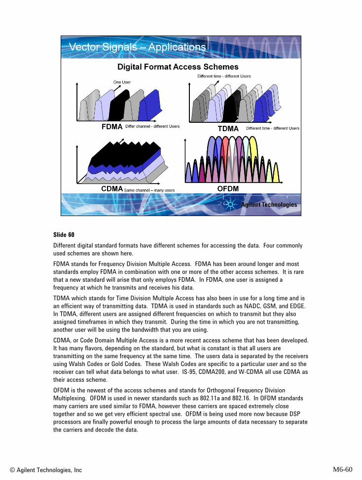
Slide 60
Different digital standard formats have different schemes for accessing the data. Four commonly
used schemes are shown here.
FDMA stands for Frequency Division Multiple Access. FDMA has been around longer and most
standards employ FDMA in combination with one or more of the other access schemes. It is rare
that a new standard will arise that only employs FDMA. In FDMA, one user is assigned a
frequency at which he transmits and receives his data.
TDMA which stands for Time Division Multiple Access has also been in use for a long time and is
an efficient way of transmitting data. TDMA is used in standards such as NADC, GSM, and EDGE.
In TDMA, different users are assigned different frequencies on which to transmit but they also
assigned timeframes in which they transmit. During the time in which you are not transmitting,
another user will be using the bandwidth that you are using.
CDMA, or Code Domain Multiple Access is a more recent access scheme that has been developed.
It has many flavors, depending on the standard, but what is constant is that all users are
transmitting on the same frequency at the same time. The users data is separated by the receivers
using Walsh Codes or Gold Codes. These Walsh Codes are specific to a particular user and so the
receiver can tell what data belongs to what user. IS-95, CDMA200, and W-CDMA all use CDMA as
their access scheme.
OFDM is the newest of the access schemes and stands for Orthogonal Frequency Division
Multiplexing. OFDM is used in newer standards such as 802.11a and 802.16. In OFDM standards
many carriers are used similar to FDMA, however these carriers are spaced extremely close
together and so we get very efficient spectral use. OFDM is being used more now because DSP
processors are finally powerful enough to process the large amounts of data necessary to separate
the carriers and decode the data.

© Agilent Technologies, Inc M6-61
Slide 61
In a signal generator, the combination of the baseband generator and the IQ modulator produce a
digitally modulated signal. The filtering and modulation type are determined by the shape of the
baseband waveforms.
To accurately simulate a digital modulated signal, however, the signal generator must do more
than just output the proper modulation. Most digital communication formats, in an effort to
conserve bandwidth, have some access scheme and the signal generator must be capable of
simulating that access scheme.
For example, a GSM signal is a popular cellular technology that has multiple users on the same
frequency. There are different timeslots that must be configured with the proper symbol rate,
modulation type, and burst profiles. The timeslots themselves must also have the proper framing
data so that a GSM receiver will recognize the incoming signal.

© Agilent Technologies, Inc M6-62
Slide 62
The sensitivity of a receiver is the lowest possible signal level that can be reliably detected and is
one of the key specifications for a receiver. For digital receivers, sensitivity is defined as the level
of the received signal that produces a specified bit error rate (BER) when the signal is modulated
with a specified psuedo-random binary sequence (PRBS) of data. In R&D testing, they will actually
determine what that level is. In manufacturing test, they will simply set the power of the signal
generator to the specified power level and determine whether or not the BER passes or fails. This
takes much less time.
© Agilent Technologies, Inc M6-63
Slide 63
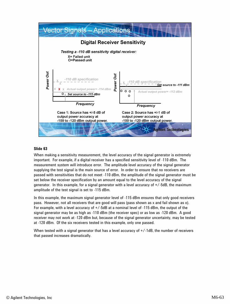
When making a sensitivity measurement, the level accuracy of the signal generator is extremely
important. For example, if a digital receiver has a specified sensitivity level of -110 dBm. The
measurement system will introduce error. The amplitude level accuracy of the signal generator
supplying the test signal is the main source of error. In order to ensure that no receivers are
passed with sensitivities that do not meet -110 dBm, the amplitude of the signal generator must be
set below the receiver specification by an amount equal to the level accuracy of the signal
generator. In this example, for a signal generator with a level accuracy of +/-5dB, the maximum
amplitude of the test signal is set to -115 dBm.
In this example, the maximum signal generator level of -115 dBm ensures that only good receivers
pass. However, not all receivers that are good will pass (pass shown as x and fail shown as o).
For example, with a level accuracy of +/-5dB at a nominal level of -115 dBm, the output of the
signal generator may be as high as -110 dBm (the receiver spec) or as low as -120 dBm. A good
receiver may not work at -120 dBm but, because of the signal generator uncertainty, may be tested
at -120 dBm. Of the six receivers tested in this example, only one passed.
When tested with a signal generator that has a level accuracy of +/-1dB, the number of receivers
that passed increases dramatically.

© Agilent Technologies, Inc M6-64
Slide 64
Sometimes you need to measure the receiver sensitivity before all of the hardware blocks are
available. Normally, BER measurements are only possible when the entire receiver is available
because to measure the BER you need all of the baseband processing to enable you access to the
payload data. Newer hardware and software development within test equipment now allows you
to measure the BER when only portions of the receiver is available.
This new technique is called Connected Solutions. With this technique, simulation software and
the test equipment must work together to be able to make the measurement. When making a BER
measurement, you must know what is created in the signal generator and you must be able to
compare that data to the data that is sent through the DUT. So the same simulation software that
creates the input waveform must also accept the post-DUT waveform and make the measurement.
In this measurement, we create a signal with the simulation tool and send it to the arbitrary
waveform generator (AWG) of the vector signal generator. This signal is played through the DUT
and captured with a signal analyzer. This captured waveform is then sent back to the simulation
tool to be analyzed. The interfaces that you use for this new kind of measurement can be RF, IF,
Analog IQ, or Digital IQ.

© Agilent Technologies, Inc M6-65
Slide 65
Adjacent and alternate channel selectivity measures the receiver's ability to process a desired
signal while rejecting a strong signal in an adjacent channel or alternate channel. An adjacent or
alternate channel selectivity test setup is shown above.
One signal generator inputs a test signal at the desired channel frequency at a level above the
sensitivity of the receiver. The second signal generator outputs either the adjacent channel signal,
offset by one channel spacing, or the alternate channel signal, offset by two channel spacings.
The output of the out-of-channel signal is increased until the sensitivity is degraded to a specified
level.
Frequency and amplitude (level) accuracy and the spectral characteristics of the test and
interfering signal are important.
Poor frequency accuracy will cause the signals to be either too close or too far from each other
and from the filter skirts. This can have the effect of appearing to improve or degrade the receiver
performance.
We saw how level accuracy can affect the sensitivity measurement of a receiver. With two
signals, the problems associated with inaccurate signals are compounded.
The SSB phase noise of the interfering signal is a very critical spectral characteristic. The test is a
measure of the performance of the receiver's IF filters. As the signal in the adjacent-channel is
increased, the rejection of the IF filter outside the passband is eventually exceeded. If the phase
noise energy inside the passband is detected, the receiver may appear to fail the test.
High levels of spurs can also degrade the selectivity measurement of a receiver. Signal generator
spurs that fall within the passband of the receiver will contribute to the overall noise level in the

passband.
© Agilent Technologies, Inc. 2007 M6-65

© Agilent Technologies, Inc M6-66
Slide 66
In a digital transmitter, adjacent channel power is mainly a function of the non-linear
characteristics of amplifiers used in the design. The in-channel digitally modulated signal spans a
certain bandwidth in frequency. Remember that amplifiers with multiple input signals can create
intermodulation distortion products so that with the many frequencies present in a digitally
modulated signal, these out-of-channel distortion products look like increased noise. This out-of-
channel non-linear intermodulation distortion for a digitally modulated signal is often referred to as
spectral re-growth.
Spectral regrowth for an digitally modulated signal is determined by measuring its adjacent
channel power. Adjacent channel power ratio is the ratio of the power in the spectral regrowth
sidebands to the power in the main channel.
When measuring an amplifier, the spectral regrowth, or ACPR performance, of the signal generator
should be less than that of the amplifier under test. The lower the ACPR performance of the signal
generator, the more accurately the ACP can be measured on the DUT. To minimize the
contribution of the vector signal generator, choose one with ACP that is approximately > 10 dB
lower in ACP than the ACP you are trying to measure.
© Agilent Technologies, Inc M6-67
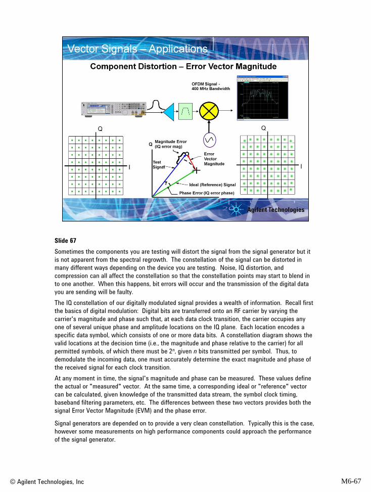
Slide 67
Sometimes the components you are testing will distort the signal from the signal generator but it
is not apparent from the spectral regrowth. The constellation of the signal can be distorted in
many different ways depending on the device you are testing. Noise, IQ distortion, and
compression can all affect the constellation so that the constellation points may start to blend in
to one another. When this happens, bit errors will occur and the transmission of the digital data
you are sending will be faulty.
The IQ constellation of our digitally modulated signal provides a wealth of information. Recall first
the basics of digital modulation: Digital bits are transferred onto an RF carrier by varying the
carrier's magnitude and phase such that, at each data clock transition, the carrier occupies any
one of several unique phase and amplitude locations on the IQ plane. Each location encodes a
specific data symbol, which consists of one or more data bits. A constellation diagram shows the
valid locations at the decision time (i.e., the magnitude and phase relative to the carrier) for all
permitted symbols, of which there must be 2n, given n bits transmitted per symbol. Thus, to
demodulate the incoming data, one must accurately determine the exact magnitude and phase of
the received signal for each clock transition.
At any moment in time, the signal's magnitude and phase can be measured. These values define
the actual or "measured" vector. At the same time, a corresponding ideal or "reference" vector
can be calculated, given knowledge of the transmitted data stream, the symbol clock timing,
baseband filtering parameters, etc. The differences between these two vectors provides both the
signal Error Vector Magnitude (EVM) and the phase error.
Signal generators are depended on to provide a very clean constellation. Typically this is the case,
however some measurements on high performance components could approach the performance
of the signal generator.

© Agilent Technologies, Inc M6-68
Slide 68
Using EVM as a metric, that same 400 MHz OFDM signal measured in the I/Q plane yields –30 dB
(or 3.3%) EVM. Although the constellation appears quite clean visually, the poor performance is
clearly visible in the error vector spectrum measurement. The performance increasingly degrades
as the band edges are approached. By convention, EVM is reported as a percentage of the ideal
peak signal level, usually defined by the constellation's corner states.
EVM and phase error are the two principal parameters for evaluating the quality of a digitally
modulated signal.

© Agilent Technologies, Inc M6-69
Slide 69
Now we are going to see how simulating real life signals will ease the testing burden.
© Agilent Technologies, Inc M6-70
Slide 70
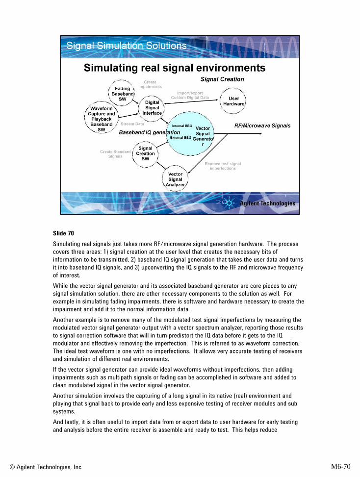
Simulating real signals just takes more RF/microwave signal generation hardware. The process
covers three areas: 1) signal creation at the user level that creates the necessary bits of
information to be transmitted, 2) baseband IQ signal generation that takes the user data and turns
it into baseband IQ signals, and 3) upconverting the IQ signals to the RF and microwave frequency
of interest.
While the vector signal generator and its associated baseband generator are core pieces to any
signal simulation solution, there are other necessary components to the solution as well. For
example in simulating fading impairments, there is software and hardware necessary to create the
impairment and add it to the normal information data.
Another example is to remove many of the modulated test signal imperfections by measuring the
modulated vector signal generator output with a vector spectrum analyzer, reporting those results
to signal correction software that will in turn predistort the IQ data before it gets to the IQ
modulator and effectively removing the imperfection. This is referred to as waveform correction.
The ideal test waveform is one with no imperfections. It allows very accurate testing of receivers
and simulation of different real environments.
If the vector signal generator can provide ideal waveforms without imperfections, then adding
impairments such as multipath signals or fading can be accomplished in software and added to
clean modulated signal in the vector signal generator.
Another simulation involves the capturing of a long signal in its native (real) environment and
playing that signal back to provide early and less expensive testing of receiver modules and sub
systems.
And lastly, it is often useful to import data from or export data to user hardware for early testing
and analysis before the entire receiver is assemble and ready to test. This helps reduce

development costs by finding design problems much earlier in the development process.
© Agilent Technologies, Inc. 2007 M6-70
© Agilent Technologies, Inc M6-71
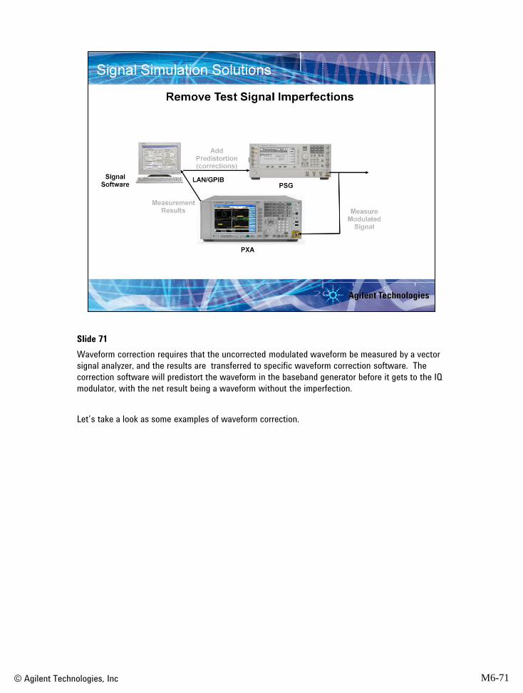
Slide 71
Waveform correction requires that the uncorrected modulated waveform be measured by a vector
signal analyzer, and the results are transferred to specific waveform correction software. The
correction software will predistort the waveform in the baseband generator before it gets to the IQ
modulator, with the net result being a waveform without the imperfection.
Let’s take a look as some examples of waveform correction.

© Agilent Technologies, Inc M6-72
Slide 72
One imperfection of a vector signal generator will be the amplitude flatness of the IQ modulator. A
modulated signal will exhibit a certain amount of amplitude tilt, ripple and roll off across the
passband of the modulation bandwidth.
© Agilent Technologies, Inc M6-73
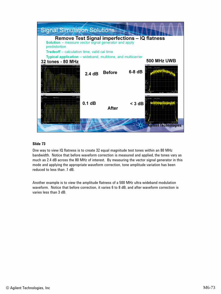
Slide 73
One way to view IQ flatness is to create 32 equal magnitude test tones within an 80 MHz
bandwidth. Notice that before waveform correction is measured and applied, the tones vary as
much as 2.4 dB across the 80 MHz of interest. By measuring the vector signal generator in this
mode and applying the appropriate waveform correction, tone amplitude variation has been
reduced to less than .1 dB.
Another example is to view the amplitude flatness of a 500 MHz ultra wideband modulation
waveform. Notice that before correction, it varies 6 to 8 dB, and after waveform correction is
varies less than 3 dB.

© Agilent Technologies, Inc M6-74
Slide 74
In-band IMD refers to the intermodulation products that fall within the channel bandwidth
of the generated signal. This type of distortion is particularly undesirable since it cannot
be filtered and directly interferes with the signal of interest. Similar to removing carrier
feedthrough, this predistortion technique generates a canceling tone at the IMD
frequency that is 180 degrees out of phase with the distortion product. This approach
uses a spectrum analyzer to measure the IMD of the original test stimulus. Then based on
these measurements, a predistorted waveform is created to remove the in-band, as well
as the out-of-band IMD products. As shown in the before and after predistortion
measurements, exceptional distortion suppression is achievable. For this test stimulus,
over 40 dB improvement was obtained.

© Agilent Technologies, Inc M6-75
Slide 75
Remember back in Slide 68, we viewed a spectral measurement of an OFDM signal that spanned
400 MHz? In this situation there are many frequency dependent components that will add or
subtract from constant group delay over that bandwidth. In this example, we used EVM as a
measure of how constant the group delay is. Before any correction is applied we measure 3.3%
EVM and most of this variation is at the edges of the band. By measuring and applying corrections
to the vector signal generator, EVM has been reduced (improved) from 3.3% to 2%. Notice that
the majority of the improvement is around the band edges of the modulated signal.
© Agilent Technologies, Inc M6-76
Slide 76
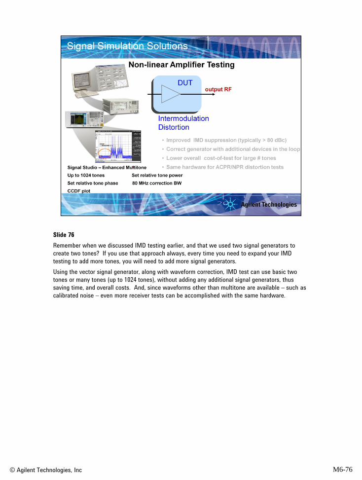
Remember when we discussed IMD testing earlier, and that we used two signal generators to
create two tones? If you use that approach always, every time you need to expand your IMD
testing to add more tones, you will need to add more signal generators.
Using the vector signal generator, along with waveform correction, IMD test can use basic two
tones or many tones (up to 1024 tones), without adding any additional signal generators, thus
saving time, and overall costs. And, since waveforms other than multitone are available – such as
calibrated noise – even more receiver tests can be accomplished with the same hardware.

77
78

79

80

© Agilent Technologies, Inc M6-81
Slide 78
The cost of operating a radar test range with live targets is incredibly expensive. By
recording signals and playing them back on a vector signal generator in the lab you save
time and money. Using the right hardware, unique waveforms can be captured in the field
and played back in the laboratory.
The file format must be converted to binary in order to be compatible with Baseband
Studio for waveform capture and playback. A free utility is available from Agilent to
facilitate this conversion.
The PXA with Option B1X (160MHz Analysis Bandwidth, 14 Bit ADC, 75 db spurious free
dynamic range) can make the following recordings;
1. At 160MHz span the PXA makes a 3 second recording.
2. At 1MHz span the PXA makes a 200 second recording.

© Agilent Technologies, Inc M6-82
Slide 80
84
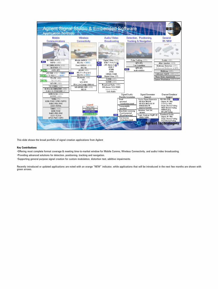
This slide shows the broad portfolio of signal creation applications from Agilent
Key Contributions
•Offering most complete format coverage & meeting time-to-market window for Mobile Comms, Wireless Connectivity, and audio/video broadcasting.
•Providing advanced solutions for detection, positioning, tracking and navigation.
•Supporting general purpose signal creation for custom modulation, distortion test, additive impairments.
Recently introduced or updated applications are noted with an orange “NEW” indicator, while applications that will be introduced in the next few months are shown with green arrows.

© Agilent Technologies, Inc. 2007 M6-86

© Agilent Technologies, Inc M6-87