this report was prepared as an account of work sponsored by …
TRANSCRIPT

This report was prepared as an account of work sponsored by an agency of the United States Government. Neither the United States Government nor any agency thereof, nor any of their employees, makes any warranty, express or implied, or assumes any legal liability or responsibility for the accuracy, completeness, or usefulness of any information, apparatus, product, or process disclosed, or represents that its use would not infringe privately owned rights. Reference herein to any specific commercial product, process, or service by trade name, trademark, manufacturer, or otherwise, does not necessarily constitute or imply its endorsement, recommendation, or favoring by the United States Government or any agency thereof. The views and opinions of authors expressed herein do not necessarily state or reflect those of the United States Government or any agency thereof.

1
Quantum Information Science
Factual Document for the Office of Basic Energy
Sciences at the Department of Energy
Prepared for the Basic Energy Sciences Roundtables on
Opportunities for Basic Research for Next-Generation Quantum Systems October 30–31, 2017
Opportunities for Quantum Computing in Chemical and Materials Sciences October 31–November 1, 2017
D. J. Dean, ORNL E. Dumitrescu, ORNL S. Economou, Virginia Tech P. G. Evans, ORNL T. Humble, ORNL S. Jesse, ORNL S. Kais, Purdue S. Kalinin, ORNL B. Lawrie, ORNL
P. Lougovski, ORNL T. Maier, ORNL F. Mohiyaddin, ORNL B. Monroe, University of Maryland W. D. Oliver, Massachusetts Institute of Technology
R. Pooser, ORNL M. Saffman, University of Wisconsin–Madison
October 19, 2017

2
Table of Contents Introduction .............................................................................................................................. 3
Principles of Quantum Computing ......................................................................................... 6
Materials for Quantum Computing Devices ........................................................................ 10 Trapped Ions ..................................................................................................................................... 10 Neutral Atoms .................................................................................................................................. 11 Silicon Spins ...................................................................................................................................... 13 Superconducting Nanowires .............................................................................................................. 16 Superconducting Qubits .................................................................................................................... 18 Color Center Spins ............................................................................................................................ 21 Photonic Quantum Computing .......................................................................................................... 23
Quantum Computing Interconnects .................................................................................... 28
Atom-by-Atom Manipulation for Building Quantum Devices ............................................ 30
Scientific Applications of Quantum Computing ................................................................. 32 Computational Chemistry .................................................................................................................. 32 Computational Materials Science ...................................................................................................... 34 Correlated Electron Systems.............................................................................................................. 34 Classical Challenges ........................................................................................................................... 34 Quantum Promise ............................................................................................................................. 35 Quantum Challenges and Outlook ..................................................................................................... 35
Quantum Characterization and Control .............................................................................. 37 Quantum Sensing with Squeezed Light .............................................................................................. 37 Squeezed Light Generation ............................................................................................................... 38 Characterization and Control of Material Dynamics with Entanglement ............................................. 38 Quantum Magnetometry .................................................................................................................. 39 Coherence in Quantum Matter .......................................................................................................... 40 Managing Coherence between Quantum Light and Quantum Matter ................................................. 41 Coherent Photon-Phonon Interactions .............................................................................................. 41 Atomic Sensing and Simulation.......................................................................................................... 41
Glossary of Terms ................................................................................................................... 43
References ............................................................................................................................. 45

3
IntroductionFor decades, scientists have known that devices to store and manipulate information in quantum physical systems such as atoms or photons would provide radical new capabilities in computing, communication, and sensing. These novel capabilities include speed-ups in scientific calculations of quantum materials and chemical systems, enhanced resolution in imaging and detection systems, and greater security for encrypted communication systems. Building these devices requires a detailed understanding of how quantum materials behave, accurate knowledge of how to integrate them, and high-fidelity control of the physical qubits that store information. These goals are fundamental research challenges for materials synthesis, fabrication, and characterization; and the science of quantum information intersects heavily with ongoing basic research into materials science, chemistry, and quantum physics. These systems represent state-of-the-art approaches to building and controlling the basic physical elements of quantum information. Research into quantum sensing and quantum communication strongly leverages these advances for next-generation technologies, e.g., measurements beyond the Heisenberg limit, while applications of quantum computing (QC) as a platform for understanding future quantum material systems highlight its potential for advanced scientific discovery.
As existing computing technologies approach fundamental limits to continued scalability, QC has emerged as a profoundly different and powerful way of computing. By exploiting the novel laws of quantum physics, QC promises to open new scientific and industrial frontiers by transforming some hard, conventional computing problems into tractable and scalable forms. However, the development of practical QC technology is a grand challenge requiring significant advances in material science, device physics, hardware and system engineering, and computer science.
Quantum bits (qubits) are the basic physical building blocks of any future quantum computer or coprocessor. A handful of different technologies have been pursued in recent years to demonstrate qubits. While each of these technologies shows promise, qubits of sufficiently high quality and quantity to perform large-scale QC remain an elusive goal. QC requires many qubits that can be initialized into predefined quantum states, manipulated to process information, and measured to extract computational results. In addition, qubits must reliably store the prepared quantum state between successive operations. The effectiveness of a qubit for these tasks therefore depends on the fundamental physical interactions between the qubit and its local environment, particularly the electric, magnetic, and phonon environments. Despite progress to minimize these unwanted interactions, current state-of-the-art efforts cannot measure, model, or predict the qubit environment with sufficient accuracy to enable the large-scale fabrication of high-quality qubits needed for mission-scale QC.
Another difficulty is that the best qubits developed to date must be individually addressed and controlled under extremely low temperature and high vacuum. These extreme environments introduce significant challenges to transmitting signals in and out of qubit registers with high bandwidth, high spatial density, high integrity, and high mechanical robustness while crossing large thermal gradients. These engineering challenges have only begun to be addressed.
Finally, there are significant open questions regarding how to use qubits effectively as computational resources. As basic units of information, qubits obey logical rules that are very different from those governing conventional bits and often unintuitive. Consequently, nascent quantum programming models are quite different from traditional computer programming models and not nearly as well understood. Moreover,

4
some core quantum algorithms show significant promise for computational speedups for physical science applications, such as electronic structure calculations for materials and chemistry, but these algorithms have been worked out for only a small set of problems with practical interest. Pending real-world applications do not yet define the interplay between quantum and traditional computation; and the broader understanding of quantum and traditional programming models, as well as quantum and conventional computing hardware, is lacking.
This factual status document for Quantum Information Science has been developed for the Department of Energy Office of Science, Basic Energy Sciences (BES). The following are several seminal or key references for interested readers; the reference section gives a more exhaustive, but still not complete, list of important papers in this area.
1. J. I. Cirac, P. Zoller, “Quantum computations with cold trapped ions,” Phys. Rev. Lett. 74, 4091 (1995).
2. C. Monroe and J. Kim, “Scaling the ion trap quantum processor,” Science 339, 1164 (2013).
3. M. Saffman, T. G. Walker, and K. Mølmer, “Quantum information with Rydberg atoms,” Rev. Mod. Phys. 82, 2313 (2010).
4. B. E. Kane, “A silicon-based nuclear spin quantum computer,” Nature 393, 133 (1998).
5. C. D. Hill, E. Peretz. S. J. Hile, M. G. House, M. Fuechsle, S. Rogge, M. Y. Simmons and L.C.L. Hollenberg, “A surface code quantum computer in silicon,” Sci. Adv. 1, 9 (2015).
6. J. L. O’Brien, A. Furusawa, and J. Bucolic, “Photonic quantum technologies,” Nat. Photonics 3, 687 (2009).
7. R. Ascender and H. J. Briegel. “A One-Way Quantum Computer,” Phys. Rev. Lett. 86, 5188 (2001).
8. D. M. Eigler and E. K. Schweizer, “Positioning single atoms with a scanning
tunneling microscope,” Nature 344, 524 (1990).
9. K. Morgenstern, N. Lorente, and K. H. Rieder, “Controlled manipulation of single atoms and small molecules using the scanning tunnelling microscope,” Phys. Status Solidi B–Basic Solid State Phys. 250, 1671 (2013).
10. I. Kassal, S. P. Jordan, P. J. Love, M. Mohseni, and A. Aspuru-Guzik, “Polynomial-time quantum algorithm for the simulation of chemical dynamics,” Proc. Nat. Acad. Sci. 105, 18681 (2008).
11. A. Aspuru-Guzik, A. D. Dutoi, P. J. Love, and M. Head-Gordon, “Simulated quantum computation of molecular energies,” Science 309, 1704 (2005).
12. R. Somma, G. Ortiz, J. E. Gubernatis, E. Knill, and R. Laflamme, “Simulating physical phenomena by quantum networks,” Phys. Rev. A 65, 042323 (2002).
13. G. Ortiz, J. E. Gubernatis, E. Knill, and R. Laflamme, “Quantum algorithms for fermionic simulations,” Phys. Rev. A 64, 022319 (2001).
14. J. Biamonte, P. Wittek, N. Pancotti, P. Rebentrost, N. Wiebe, and S. Lloyd, “Quantum machine learning,” Nature 549, 195 (2017).
15. R. Babbush, D. W. Berry, I. D. Kivlichan, A. Y. Wei, P. J. Love, and A. Aspuru-Guzik, “Exponentially more precise quantum simulation of fermions in second quantization,” New J. Phys. 18, 033032 (2016).
16. F. A Zwanenburg, A. S. Dzurak, A. Morello, M. Y. Simmons, L.C.L. Hollenberg, G. Klimeck, S. Rogge, S. N. Coppersmith, and M. A. Eriksson, “Silicon quantum electronics,” Rev. Mod. Phys. 85, 961 (2013).
17. M. Veldhorst, C. H. Yang, J. C. C. Hwang, Huang, J. P. Dehollain, J. T. Muhonen, S. Simmons, A. Laucht, F. E. Hudson, K. M. Itoh, A. Morello, and A. S. Dzurak, “A two-

5
qubit logic gate in silicon,” Nature 526, 410 (2015).
18. D. Wecker, M. B. Hastings, N. Wiebe, B. K. Clark, C. Nayak, and M. Troyer, “Solving strongly correlated electron models on a quantum computer,” Phys. Rev. A 92, 062318 (2015).
19. W. D. Oliver and P. D. Welander, MRS Bulletin 18, 816 (2013)
20. G. Windlin, “Quantum information processing with superconducting circuits: a review,” Rep. Prog. Phys. 80, 106001 (2017)

6
Principles of Quantum Computing The fundamental principles of QC stem from the theory of quantum mechanics. Quantum mechanics was developed in the early 20th century to explain the behavior of a wide variety of physical systems including nuclei, atoms, electrons, and photons, as well as novel condensed matter and macromolecular systems. Among the many essential quantum concepts that impact QC are superposition, entanglement, and the uncertainty principle, i.e., intrinsic randomness that appears in quantum mechanical measurements. The application of those ideas to the theory of information led to the development of quantum information theory, from which QC originates, as well as other potential application areas such as quantum communication and quantum sensing.
In quantum information theory, the principle of superposition is used to construct new representations of information. Conventional computing is formulated using a binary representation of data and instructions, in which a register element r stores a bit b that may take on either of two values, b0 or b1. By comparison, QC also requires a physical element r to store information; but the quantum register element may now take the value of a quantum bit, or qubit, q. The qubit q expresses a superposition of binary states, e.g., value(r) = q = αb0 + βb1, in which the basis states b0 and b1 represent the quantum two-level system. For example, an electron prepared in a well-defined superposition of the orthogonal spin-up and spin-down states represents a qubit, while the electron itself represents the register. Formally, the qubit is a superposition over a complex 2-dimensional (2D) vector space with normalized coefficients, i.e., |α|2 + |β|2 = 1. This leads to a diagrammatic representation for the possible values of a qubit given as the surface of the unit sphere, the Bloch sphere. As shown in Figure 1, the opposing north and south poles of the sphere represent the classical limits of b0 = 0 and b1 = 1, respectively, while every point on the surface corresponds to a possible qubit value q.
Figure 1. The Bloch sphere illustrates the infinite set of possible values for a qubit q as the surface of the unit ball, while opposing poles of the sphere identify the classical limits of binary values b0 = 0 and b1 = 1. In practice, qubits can be realized by preparing superpositions of quantum two-level systems such as the spin-up and spin-down states of an electron. | Image courtesy of Travis Humble, Oak Ridge National Laboratory
An immediate extension of the superposition principle is to the case of more than a single quantum register element. The simplest example is a set of n independent qubits, for which each register element ri stores a value qi that is independent of any other. However, quantum mechanics permits another possibility in which multiple register elements may collectively store superpositions over multiple binary values. This phenomenon, known as “entanglement,” is a form of information that cannot be reproduced by conventional bits. The qubit register elements must remain independently addressable, but the information that they store can no longer be expressed piecewise, i.e., value(r1r2) ≠ value(r1) value(r2). For example, two qubits may be

7
entangled so that they are both in the b0 state or both in the b1 state but exclude any possibility of anti-correlated values. The implications of entanglement were central to the Einstein, Podolsky, and Rosen (EPR) paradox, which conjectured the incompleteness of quantum mechanics. EPR argued that the apparent non-local correlations between the properties of otherwise independent physical systems violated notions of locality and reality. However, Bell has since established experimental conditions to verify the existence of entanglement which have been used extensively by the QC community.
Superposition and entanglement lead to an important conceptual difference regarding how to interpret the value of a register in QC. Observing a qubit by measurement in the original basis results in a projection of the quantum state to either the b0 or b1 values. This transition from a qubit to a bit is the “collapse of the wave function” induced by measurement. The implication is that the qubit q is not a physical observable. Instead, a superposition state q = αb0 + βb1 must be interpreted with respect to the probability of observing either b0 to b1, which are defined as p0 = |α|2 and p1 = |β |2, respectively. Either of these two outcomes may be observed following measurement, and the exact measurement results cannot be predicted for any arbitrary qubit. Rather, the probabilities p0 and p1 provide the likelihood that a given outcome will be observed. In practice, practitioners of QC have learned to use this intrinsic randomness to advantage. For example, the collapse induced by measurement is useful for preparing register elements in well-defined initial states and reading out conventional binary values following a sequence of operations.
Computing with qubits requires controlling the quantum mechanical interactions between register elements. Several computational models support the implementation of universal QC, and all use different methods to transform quantum registers. The first is the gate model of QC, which applies discrete transformations called “gates” to the register elements. Formally, gates define fixed
transformations of the quantum state by controlling the short-time dynamics of the register, and a gate may act on either a single or multiple register elements. When laid out as an ordered sequence, the gates define a circuit that can express higher functionality, such as addition, multiplication, and so on. In practice, gates are implemented by driving Hamiltonian dynamics with sequences of externally applied fields. Alternatively, the adiabatic QC continuously controls the register dynamics using gradual modifications to Hamiltonian interactions. By slowly driving the dynamics, the register value can be transformed from one equilibrium configuration to another in which the initial and final configurations define the desired computation. A third model for quantum computation is topological QC, which implements computational transformations by controlling the topological order of register elements. The basis for this approach is the non-abelian exchange statistics that arise when pairs of anyonic quasiparticles are braided. Anyonic quasiparticles arise in 2D systems and demonstrate spin-statistics that generalize the concepts of bosonic and fermionic systems. Exchanges between non-abelian anyons induce non-trivial state transformations termed “braiding.” Braiding represents permutations on register elements that are formed from pairs of the anyonic quasiparticles. A key feature of this model is that the computation is stored in the degenerate ground state of the anyonic system, which offers intrinsic protection against erroneous transformations.
Realizing any of these models for QC depends on the ability to manipulate individual atoms, molecules, electrons, excitations, and photons. Reports from workshops held in 2014 and 2016 describe many of the materials and chemistry frontiers that will empower QC [1, 1a]. The idealization of a qubit as a two-level system is not easily realized in nature because of coupling with the surrounding quantum systems through various forms of electromagnetic forces. A great deal of effort has been focused on finding quantum physical systems that can be isolated from their

8
environments yet controlled with sufficient precision to perform reliable computations. Alongside state-of-the-art efforts in nanofabrication and device physics, a common approach to reduce errors is based on thermodynamic control. This approach uses cryogenic refrigeration and ultra-high vacuum to isolate register elements from as much as thermal noise as possible. Shielding from stray radiation, such as magnetic fields, is also important. In addition to these coarse-grained efforts, fine-grain control over quantum physical interactions is important for inhibiting quantum dynamics that lead to possible errors. Quantum control plays an important role in designing and operating the applied fields used to implement quantum instruction. This role includes methods for noise cancellation and error mitigation that take into account well-characterized noise sources and device physics.
Alongside physical efforts to engineer against noise, QC also makes use of quantum error correction methods that can recover from faults acquired during computation. These require redundant encoding of the stored information, which increases the number of physical resources required as well as the complexity of carrying out individual instructions. Bounds for the amount of error correction required to achieve fault-tolerant quantum computation are known to increase with the level of intrinsic noise in each gate. Therefore, substantial value is placed on minimizing the amount of intrinsic noise in physical registers to levels that can support fault-tolerant operations with minimal quantum error correction overhead.
On the path to realizing fault-tolerant quantum processors, a pre-threshold processor is a device consisting of qubits with physical error rates above the noise level required for fault-tolerant operation. These pre-threshold devices would rapidly fail if scaled up in number of qubits because of the buildup of errors brought on by decoherence and noise at the physical level.
However, the physical error rate is not the only limiting factor, as device architecture may also
restrict scalability. The concern arises that the design of pre-threshold processors may not be suitable to implement fault-tolerant quantum error–corrected operations. The emerging requirement is that enough qubits with sufficiently low physical error rates must be placed in close enough proximity and with sufficient flexibility to interconnect them as required by the error correction code and fault-tolerant protocols. Current quantum processors are therefore pre-threshold devices that do not yet implement error-corrected instruction operating below threshold.
The principles of QC arise prominently in developing applications for digital and analog quantum simulation. Whereas the revolutionary principles of quantum mechanics have provided breakthroughs in the understanding of physics at very small scales for nearly a century, these theories quickly grow in complexity and can become unwieldy. Feynman offered the early insight that the scientific models for atoms, molecules, and photons may be more efficiently represented by using other quantum mechanical systems to do these calculations. There are currently two approaches to realizing Feynman’s insight of solving the Schrödinger equation more efficiently. The first is digital quantum simulation, which solves the Schrödinger equation using a discretized approximation of the time-evolution operator. The approach of digital quantum simulation first makes use of efficient methods for constructing the system Hamiltonian and then efficiently decomposing the time-evolution operator into a sequence of well-defined instructions. These instructions are applied to the register in order to carry out a specific simulation sequence. Processors that support digital quantum simulation can, in principle, also support the execution of other quantum instruction sequences. By contrast, analog quantum simulation uses the interactions between register elements to simulate the continuous-time dynamics generated by a defined Hamiltonian. The efficiency of this method lies in direct implementation of Schrödinger’s equation. However, executing these instructions requires specific implementations of

9
the Hamiltonian which may not suffice for general-purpose QC. For either digital or analog quantum simulation, the resulting computational state represents the many-body wave function characterizing the system of interest. Subsequent evaluations may then use the wave function to
compute, e.g., expectation values of the simulated systems.
In the following sections, we describe the current status of each of these elements, beginning with hardware realizations of qubits and ending with a brief survey of applications relevant to BES.

10
Materials for Quantum Computing Devices In this section, we describe several realizations of qubits that have been recently developed and deployed.
Trapped Ions Trapped ions are qubit standards and among the leading technologies to build a quantum computer [2]. Atomic ion qubits are the basis for the most highly performing atomic clocks [3], and they can be replicated with an accuracy that cannot be matched in any other physical system. Moreover, through optical absorption and fluorescence techniques, trapped ion qubits can be initialized and measured with near-perfect efficiency. High-fidelity entangling gate operations are available through control fields that modulate the electrical repulsion between the atomic ions [4]. Controlled qubit operations with dozens of trapped ion qubits have been demonstrated in the laboratory with a room-temperature apparatus. Trapped ion technology is now being developed at a modular level with high-level considerations in gate co-design, and quantum software is beginning to guide the scaling to much larger systems.
The typical ion trap geometry for quantum information purposes is the linear radio frequency (rf) Paul trap, in which nearby electrodes hold static and dynamic electrical potentials that lead to an effective harmonic confinement of the ions [2,4]. When ions are laser-cooled to very low temperatures in such a trap, the ions form a linear crystal of qubits with the Coulomb repulsion balancing the external confinement force. An advanced chip-based, ion trap structure is shown in Figure 2. Ions are typically loaded into traps by creating a neutral atomic flux of the desired particle and ionizing them once in the trapping volume. Ions can remain confined for months, and lifetimes are often limited by the level of vacuum. Elastic collisions with residual background gases occur roughly once per hour per ion at typical ultrahigh-vacuum pressures (∼10−11 torr) and do not necessarily eject the ion. Cryogenic chambers at 4 K can virtually eliminate these collision events by further reducing the background pressure.
Figure 2. Photograph of the Sandia HOA (high optical access) microfabricated linear trap. The long slot at the center has 96 electrodes that allow the suspension of atomic ions at an altitude of 80 µm above the slot. The inset is a superimposed image of a 50-ion chain. The balance between confinement and Coulomb repulsion results in typical ion-ion spacings of 5 µm, allowing the individual optical addressing of the qubits with an array of tightly focused laser beams. | Image courtesy of Sandia National Laboratories
11
Appropriate atomic ion species should have a strong closed optical transition that allows for laser cooling of the motion, qubit state initialization, and efficient qubit readout. This rules out almost anything other than simple atomic ions with a lone outer electron, such as the alkaline earths (Be+, Mg+, Ca+, Sr+, and Ba+) and particular transition metals (Zn+, Hg+, Cd+, and Yb+). Qubits are represented by two stable electronic levels within each ion, corresponding to bit values 0 and 1. In many cases, these “atomic clock” qubit levels are first-order insensitive to magnetic fields and can exhibit coherence times in excess of 1000 seconds [5]. The qubits can be initialized and measured through standard optical pumping and state-dependent fluorescence techniques with fidelities exceeding 99.9% per qubit.
The motion of many trapped ions is coupled through the Coulomb interaction, and a natural way to implement entangling quantum logic gates between ions in a crystal is to use the motion as an intermediary by applying qubit state– dependent optical or microwave dipole forces to the ion (or ions) [4, 6,7]. Single-qubit gate fidelities greater than 99.99% have been demonstrated with trapped ion qubits, and multi-qubit entangling operations with fidelities greater than 99.9% have been achieved in the laboratory [8,9]. Experiments have commanded complete control of up to seven trapped ion qubits, with the availability of quantum gates between every possible pair of qubits [10,11]. In related experiments involving 50–200 trapped ion qubits, quantum simulations have allowed the global implementation of qubit couplings to simulate problems in quantum magnetism and other strongly interacting physical models [12,13]. One feature of the control of a module of trapped atomic ion qubits is that their connectivity can be complete and reconfigurable [10,11]. This allows potential applications to be easily adapted to any qubit graph in the trapped ion system.
Methods for scaling beyond ~100 trapped ion qubits use a multiplexed architecture called the “quantum charge-coupled device” (QCCD) [14]. It
involves the sequential entanglement of small numbers of ions through their collective motion in a single chain and the classical shuttling of individual ions between different trapping zones to propagate the entanglement. The QCCD architecture requires exquisite control of the ion positions during shuttling and may require additional atomic ion species to act as “refrigerator” ions to quench the excess motion from shuttling operations. Rudimentary versions of the QCCD idea have been used in many quantum information applications, such as teleportation and small quantum algorithms [4]; and recent experiments have shown the reliable, repeatable, and coherent shuttling of ion qubits over millimeter distances in microseconds [15] and through complex 2D junctions.
Neutral Atoms Neutral atom quantum computation is based on encoding qubits in hyperfine ground states of neutral atoms that are trapped in optical lattices, or arrays of magnetic traps in an ultra-high–vacuum environment. There are several attractive features of a neutral atom approach: (1) Hyperfine ground states are well isolated from the environment and have excellent coherence properties, with 7 s demonstrated in 2016 [16]. (2) Atoms are identical, natural qubits, so there is no additional overhead associated with calibrating and monitoring the phase evolution of inequivalent, engineered qubits. (3) Neutral atoms in their ground state have extremely weak interactions at few-micron separation and therefore serve as excellent qubit memories [17]. (4) Using Rydberg states, the atoms become strongly interacting [17], enabling entangling gates and multi-qubit gates, which are efficient for implementation of algorithms and error correction [18, 19]. (5) It is relatively straightforward to entangle atoms with optical photons, opening the prospect of distributed QC and quantum networking [20]. Atoms can also be used to provide interfaces to superconducting qubits [21] and thereby mediate networking of superconducting processors.

12
There are serious challenges that remain to be overcome for neutral atoms to be a viable approach for QC. Optical traps are typically limited to not more than an equivalent trap depth of a few millikelvin. Trapped atoms are therefore lost owing to collisions with untrapped background atoms. Vacuum-limited lifetimes of several minutes are common; but for continuous operation of a neutral atom quantum computer, atom reloading must be incorporated. Reloading has been demonstrated on a small scale [22], but not yet in a way that leaves the quantum information of neighboring qubits undisturbed. Loading of atoms into a trap array is stochastic and provides only 50–90% filling fractions. A completely filled subarray can then be prepared using atom rearrangement. This has been shown to work well with fully filled arrays of ~50 qubits prepared in a fraction of a second [23, 24], but it adds experimental complexity.
State preparation is performed with high fidelity using optical pumping and high-fidelity measurements that rely on the imaging of internal state–dependent resonance fluorescence. Although essentially perfect discrimination of the qubit states has been demonstrated, for example in Xia et al. [25], there are two outstanding challenges associated with these measurements.
First, measurements are not site specific, since scattered photons can be absorbed by neighboring atoms, thereby corrupting the qubit state. This is problematic for measurement-based error correction. Several possible solutions have been put forward, including shelving and a two-species approach [26]; but crosstalk-free measurement has not yet been demonstrated. Second, almost all measurements to date have relied on a lossy protocol that has poor scaling because atom reloading is required half of the time, on average, after the measurement. Loss-free, or at least very low-loss measurements have been demonstrated, but only on single atoms or small arrays [27, 28, 29, 30]. Lossless measurements need to be demonstrated on large arrays to prove scalability.
High-fidelity single qubit gates have been demonstrated in 1-dimensional (1D) [31], 2D [25], and 3-dimensional (3D) [16] arrays of up to about 50 qubits with gate times ranging from sub-microseconds [31] to a few hundred microseconds [16] and randomized benchmarking fidelity of close to 0.999. Two-qubit CNOT gates and two-qubit entanglement using Rydberg interactions [32] have been demonstrated by a few groups. The best results to date demonstrate a Bell state fidelity of 0.73 [33] and a post-selected (against atom loss) fidelity of 0.81 [34]. The low two-qubit gate fidelity currently limits the utility of a neutral atom approach and remains a significant hurdle. Recent theory has shown that Bell state fidelity of 0.9999 –0.99999 should be possible [35, 36], but an experimental demonstration is still missing.
All neutral atom qubit experiments to date have used heavy alkali atoms, either rubidium or cesium. Alkaline earths and lanthanides provide some intriguing opportunities for improved performance but remain relatively less developed.
If a high-fidelity, two-qubit gate can be demonstrated; atom reloading can be incorporated into an array experiment; and crosstalk-free, lossless measurements can be performed, then neutral atoms will have great potential for scalability [37, 38]. Either a 10,000 qubit 2D array or a million qubit 3D array would occupy an area only 0.5 mm on a side. Taking advantage of this scaling potential will require developments in lasers and beam scanning optics. Higher laser power, probably approaching several tens of watts, will be needed for large arrays. An alternative is magnetic trap arrays, but this approach is less well developed [39]. Another challenge is fast beam scanning to individual qubit sites. A variety of technologies are available [40], but none have adequate time-bandwidth product to take full advantage of very large qubit arrays. Further development of beam scanning technology would benefit neutral atom QC progress.

13
Silicon Spins Spins in silicon are attractive candidates for qubits because of their compactness, spanning length-scales of few tens of nanometers; long spin relaxation and spin coherence times of several seconds; and similar fabrication techniques to those used in the silicon microelectronics industry. The past 5 years have witnessed advancements in demonstrating single- and two-qubit operations with silicon spin qubits on two major platforms: (1) electron and nuclear spins of donor impurities embedded into a silicon lattice and (2) electron spins in electrostatically defined silicon quantum dots. The following subsections describe the two platforms, including their implementation, recent results, advantages, drawbacks, and challenges.
Donor (31P) spins in silicon The use of the nuclear and electronic spin states of atomic donors such as 31P for qubits was first suggested by Kane in 1998 [41]. Each of these two-level systems is capable of encoding a qubit of information, while single-qubit operations correspond with controlling the spin state applying a global oscillating magnetic field on spin resonance. The control frequency of each qubit is determined by the hyperfine coupling between the nuclear and electronic spin states and can be electrically tuned by applying static fields from nearby gate electrodes. Two-qubit operations are performed by tuning the spin exchange coupling between nearby donor electrons using additional gate electrodes.
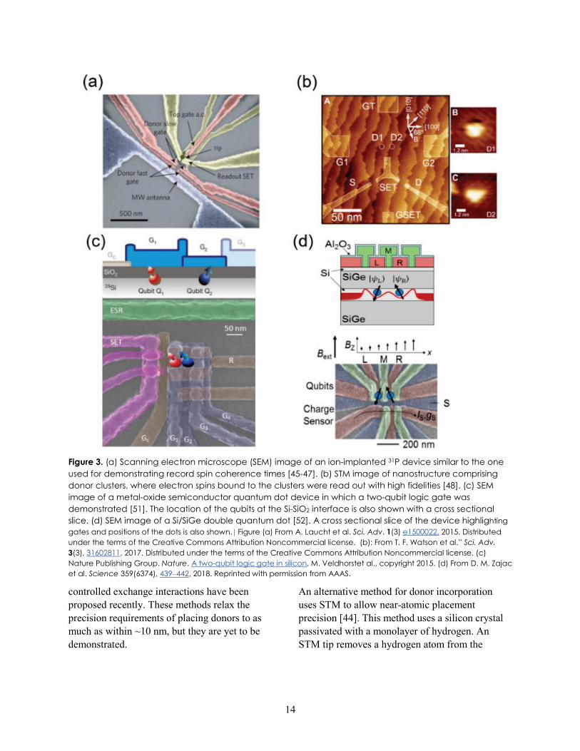
There are two popular methods of controllably incorporating the atomic donors into the bulk silicon substrate needed for the Kane proposal and its recent variants [42, 43]: (1) ion implantation, and (2) scanning tunneling microscopy (STM). In the first technique, donors are ion-implanted into a silicon substrate coated with a thermally grown thin (~10 nm) oxide. Implantation is augmented with methods that allow counting each donor that enters the silicon substrate [44]. Device fabrication then deposits aluminum gates on the oxide layer to electrostatically control the donor orbital and spin
energy levels. This also aids in the creation of charge reservoirs, as required for single-electron transistors, at the Si-SiO2 interface for reading out the donor electron spin (Figure 3) [44]. Al2O3 (grown by oxidation of gates) electrically isolates gates that are stacked above each other. A microwave antenna is placed near the donor, which generates oscillating magnetic fields for controlling the donor spins. Recent progress includes
1. Readout and control of both the electron and nuclear spins of single 31P donors in ion-implanted devices [44]
2. Extension of the coherence times of 31P qubits to several seconds with isotopic purification and advanced filtering techniques [45]
3. Electrical modulation of the hyperfine coupling and resonance frequency of 31P spins [46]
4. Demonstration of a quantum memory with the 31P nuclear spin acting as a memory for the electron spin qubit [47].
The ions are implanted with high energy into the lattice, leading to “straggle,” or placement inaccuracies, that can be as large as 10 nm, which is on the order of critical feature sizes in the Kane device architecture. Recall that the Kane proposal required exchange coupling between two donor electrons for two-qubit gate operation. This electron-electron coupling is extremely sensitive to the position and separation between donors, necessitating precise donor placement accuracy (within 1 nm) and/or tunability by several orders of magnitude [44]. In prior experimental demonstrations, several donors were implanted near the gates to overcome straggle, so that few donors were in the appropriate positions for their spins to be read out and controlled. Although this approach is sufficient for demonstrating single- and two-qubit gate operation, scaling up such devices to several qubits is impractical when it is reliant on the exchange coupling. Alternate methods of coupling two donor qubits via the magnetic or electric dipoles of the electrons [42, 43], microwave resonators [43], and hyperfine
14
Figure 3. (a) Scanning electron microscope (SEM) image of an ion-implanted 31P device similar to the one used for demonstrating record spin coherence times [45-47]. (b) STM image of nanostructure comprising donor clusters, where electron spins bound to the clusters were read out with high fidelities [48]. (c) SEM image of a metal-oxide semiconductor quantum dot device in which a two-qubit logic gate was demonstrated [51]. The location of the qubits at the Si-SiO2 interface is also shown with a cross sectional slice. (d) SEM image of a Si/SiGe double quantum dot [52]. A cross sectional slice of the device highlighting gates and positions of the dots is also shown. | Figure (a) From A. Laucht et al. Sci. Adv. 1(3) e1500022, 2015. Distributed under the terms of the Creative Commons Attribution Noncommercial license. (b): From T. F. Watson et al.” Sci. Adv. 3(3), 31602811, 2017. Distributed under the terms of the Creative Commons Attribution Noncommercial license. (c) Nature Publishing Group. Nature. A two-qubit logic gate in silicon, M. Veldhorstet al., copyright 2015. (d) From D. M. Zajac et al. Science 359(6374), 439–442, 2018. Reprinted with permission from AAAS.
controlled exchange interactions have been proposed recently. These methods relax the precision requirements of placing donors to as much as within ~10 nm, but they are yet to be demonstrated.
An alternative method for donor incorporation uses STM to allow near-atomic placement precision [44]. This method uses a silicon crystal passivated with a monolayer of hydrogen. An STM tip removes a hydrogen atom from the
15
surface where a 31P atom needs to be incorporated. Phosphene gas is then diffused onto the substrate so that the 31P atoms bind with the silicon atoms underneath. The remaining hydrogen atoms are removed from the surface, and an overgrowth of silicon is then epitaxially grown. Highly doped 31P regions fabricated with this method may also be created in the plane with the qubit donors to constitute electrodes for qubit readout and readout. Recent advancements realized with STM-incorporated donors include
• demonstration of a single-atom transistor [44]
• realization of nanowires less than three atoms wide [44]
• high-fidelity readout of electrons bound to clusters of 31P atoms [48]
• observation of exchange coupling between electrons in 31P clusters
• spin control of electrons in 31P clusters.
Although STM offers near-atomic donor placement accuracy, it is not entirely deterministic with regard to the number of donors that end up being incorporated at each location. As a result, experiments on these nanostructures are conducted on electrons bound to clusters (1–of donors (Figure 3b). Scaling up such devices also leads to uncertainties in the exchange coupling among the electrons bound to adjacent clusters, necessitating high tunability. Additionally, the low thermal budget in the STM method complicates the growth of a high-quality insulating oxide close to the plane that contains the donor, and it has so far hindered the ability to electrostatically control donors through metal gates on the top. Efforts to realize STM-incorporated qubits and gates in 3D arrays, in the absence of an oxide, are ongoing.
Silicon dots An alternative silicon qubit technology uses quantum dots electrostatically induced at a material interface, such as Si-SiO2 or Si-SiGe, with gate electrodes. The spin of the electron in the dot encodes quantum information and is
controlled via electric or magnetic spin resonance. Charge reservoirs are defined at the interface to read out the qubits. Two-qubit operations are performed with the exchange coupling between dot electrons, which can also be electrostatically modified. Such dots have the advantage of being extremely tunable using voltages applied to the gate electrodes that define them. There are two popular pathways for implementing quantum dot silicon spin qubits: (1) metal-oxide-semiconductor (MOS) quantum dots and (2) Si-SiGe quantum dots. In MOS quantum dots, aluminum gates are deposited on a silicon substrate coated with a thin (~10 nm) oxide. The gates are biased appropriately to induce quantum dots at the Si-SiO2 interface (Figure 3c) [44]. Qubit control is via spin resonance from magnetic fields generated by a microwave antenna near the dot. Recent advancements with MOS quantum dots include
• full control of electron number (1–25) in the dot [44]
• spectroscopy and tunability of orbital (valley) energy states in the dot by several 100 µeV with electric field [49]
• readout and control of the electron spin qubit in the dot [50]
• demonstration of two-qubit gate operation with tunable exchange couplings [51]
Compared with donors with electrons naturally bound by the 31P Coulomb potential, quantum dots require more gates to confine and control the dot electron. This leads to increased material strain arising from the mismatch between the thermal expansion coefficients of silicon and aluminum. Cooling the device down to milli-Kelvin temperatures for operation alters the lattice potential and the position of the electrons and may induce accidental dots at the interface. Replacing aluminum with polysilicon can reduce strain, as silicon and polysilicon have more similar thermal coefficients. Additionally, the excited valley-orbital energy states in MOS quantum dots are closer to the ground orbital states (by several

16
100 µeV) compared with those in 31P donors (~10 MeV) [44]. The excited states can potentially accelerate the relaxation of donor electron spin qubits via spin-orbit coupling [49]. This issue can be mitigated, as the separation between the splitting between valley states is tunable with electric fields and has been shown to exceed 700 µeV in experimental dot devices [49]. Theory predicts valley splitting also to be severely depressed by the surface roughness at the interface, as well as by electric field [49]. A challenge with MOS dots as well as ion-implanted donors is the variability (more than 0.5 V) of the device threshold voltage due to uncontrolled defects and charges at the Si-SiO2 interface. All the above parameters (strain, roughness, and defects) depend on fabrication processes and vary between devices, thereby affecting the qubit reproducibility.
For Si-SiGe quantum dots, the device topology is as follows: a linearly graded SiGe buffer substrate is epitaxially grown on top of a silicon wafer. The buffer is then polished before the growth of a 200 nm thick Si0.7Ge0.3 layer, an 8 nm thick silicon quantum well, a 50 nm thick Si0.7Ge0.3 spacer, and an ~2 nm thick silicon cap [52]. Aluminum gates are deposited on the silicon cap and biased to induce the dot in the quantum well (Figure 3d). A cobalt micro-magnet is integrated on the chip and produces a magnetic field gradient. The electron is electrostatically shifted back and forth within the field gradient, thereby experiencing an oscillating magnetic field, which results in electrically driven spin resonance and control. Recent results with Si-SiGe quantum dots include realization of a single-electron spin qubit in the dot, controlled electrically with gate voltages [53], (2) demonstration of a CNOT gate between two electron spins in the dots [52], and (3) a two-qubit programmable quantum processor capable of performing the Deutsch-Jozsa and Grover algorithm [54]. A significant challenge in Si-SiGe quantum dots is the low valley splitting (a few tens of µeV), which is much smaller than in MOS quantum dots. The presence of the low-lying valley-orbit state leads to fast decoherence of the
spin qubits and is dependent on strain, defects, and step edges in the quantum wells [44].
Although silicon qubits offer the promise of similar fabrication methods to those used in the semiconductor industry, atomic details (such as defects, donor placement errors, strain, and surface roughness) that affect the quality and reproducibility of qubits have been unaddressed so far by the industry. To scale up current demonstrations to a several-qubit quantum processor, these atomic details must be addressed and their variation in and between devices must be minimized; doing so will require extensive fabrication capabilities, along with device and material characterization techniques.
Superconducting Nanowires Majorana zero modes (commonly referred to as Majorana fermions because of historic connections with the self-conjugate elementary fermionic particles proposed by Ettore Majorana in 1937) are emergent non-abelian quasiparticles that serve as their own antiparticles. Majorana fermions offer a promising route to realization of the non-abelian anyons required by the topological QC model [55]. Unlike fermions or bosons, whose multi-particle wavefunctions respectively acquire a phase of −1 or +1 under particle exchange, Majorana modes are Ising type non-abelian anyons whose mutual exchanges perform non-trivial quantum operations on their joint states. The quantum state of a collection of Majorana fermions is determined by the braiding configuration of the many particles’ space-time paths. The world lines of Majoranas form braids that are determined solely by topology and cannot be easily deformed by localized perturbations or fluctuations. Majorana-based qubit technologies aim to harness these exotic quantum statistics to perform topological computations that are naturally invariant under local perturbations.
The fundamental connection between physics and topology underpins the non-abelian character of Majorana modes and is central to their experimental realization, their role in fault-tolerant
17
quantum computations and toward analog quantum simulations. A series of important breakthroughs have led to the use of superconducting platforms for the development of Majorana qubits. After the original discovery of non-abelian physics in the fractional quantum Hall effect, an equivalence between the Moore-Read (Pfaffian) quantum Hall state and that of a p-wave superconductor (hereinafter referred to as a topological superconductor) was soon established [56,57]. Proposals to engineer effective p-wave superconductors with heterostructure devices involving common materials, such as superconducting substrates and either topological insulators [58] or strong spin-orbit coupled semiconductors [59], brought the prospect of realizing Majorana modes closer to reality.
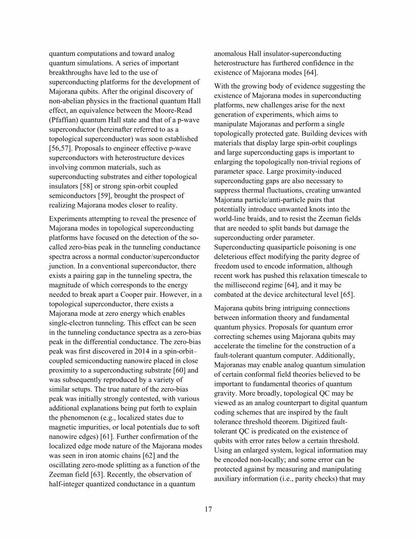
Experiments attempting to reveal the presence of Majorana modes in topological superconducting platforms have focused on the detection of the so-called zero-bias peak in the tunneling conductance spectra across a normal conductor/superconductor junction. In a conventional superconductor, there exists a pairing gap in the tunneling spectra, the magnitude of which corresponds to the energy needed to break apart a Cooper pair. However, in a topological superconductor, there exists a Majorana mode at zero energy which enables single-electron tunneling. This effect can be seen in the tunneling conductance spectra as a zero-bias peak in the differential conductance. The zero-bias peak was first discovered in 2014 in a spin-orbit–coupled semiconducting nanowire placed in close proximity to a superconducting substrate [60] and was subsequently reproduced by a variety of similar setups. The true nature of the zero-bias peak was initially strongly contested, with various additional explanations being put forth to explain the phenomenon (e.g., localized states due to magnetic impurities, or local potentials due to soft nanowire edges) [61]. Further confirmation of the localized edge mode nature of the Majorana modes was seen in iron atomic chains [62] and the oscillating zero-mode splitting as a function of the Zeeman field [63]. Recently, the observation of half-integer quantized conductance in a quantum
anomalous Hall insulator-superconducting heterostructure has furthered confidence in the existence of Majorana modes [64].
With the growing body of evidence suggesting the existence of Majorana modes in superconducting platforms, new challenges arise for the next generation of experiments, which aims to manipulate Majoranas and perform a single topologically protected gate. Building devices with materials that display large spin-orbit couplings and large superconducting gaps is important to enlarging the topologically non-trivial regions of parameter space. Large proximity-induced superconducting gaps are also necessary to suppress thermal fluctuations, creating unwanted Majorana particle/anti-particle pairs that potentially introduce unwanted knots into the world-line braids, and to resist the Zeeman fields that are needed to split bands but damage the superconducting order parameter. Superconducting quasiparticle poisoning is one deleterious effect modifying the parity degree of freedom used to encode information, although recent work has pushed this relaxation timescale to the millisecond regime [64], and it may be combated at the device architectural level [65].
Majorana qubits bring intriguing connections between information theory and fundamental quantum physics. Proposals for quantum error correcting schemes using Majorana qubits may accelerate the timeline for the construction of a fault-tolerant quantum computer. Additionally, Majoranas may enable analog quantum simulation of certain conformal field theories believed to be important to fundamental theories of quantum gravity. More broadly, topological QC may be viewed as an analog counterpart to digital quantum coding schemes that are inspired by the fault tolerance threshold theorem. Digitized fault-tolerant QC is predicated on the existence of qubits with error rates below a certain threshold. Using an enlarged system, logical information may be encoded non-locally; and some error can be protected against by measuring and manipulating auxiliary information (i.e., parity checks) that may
18
be corrupted by local interactions. Although leading conventional qubit platforms have performed initial proof-of-principle experiments demonstrating a small patch of a quantum error-correcting code, a Majorana qubit is intrinsically immune to some local perturbations. A Majorana qubit is therefore on equal footing with a logical qubit that has been redundantly encoded into hundreds of conventional qubits.
In addition to their beneficial role for QC, the physics of interacting Majorana modes has proved to be an interesting field of study in modern condensed matter physics. As illuminated by Kitaev, studying fermion and spin models from the perspective of their Majorana components sheds new light on strongly interacting systems and has broadened our understanding of many-body physics. Theoretical studies have shown that coulomb interactions may enhance the topologically non-trivial parameter regimes in which Majorana particles are experimentally realized [66]. Further, systems consisting of large numbers of randomly interacting Majorana modes have recently been found to exhibit emergent conformal symmetries thought to be connected to AdS/conformal field theory (CFT) models [67]. Interestingly, setups consisting of 2D substrates or nanowire networks, practically identical those described earlier, have been proposed as analog simulator devices for the Sanchdev-Ye-Kitaev model [68] of external black holes in 2D anti-de Sitter space. [68]. In the near future, devices based on these proposals could be used to perform otherwise intractable quantum simulations that double as benchmarking protocols—evaluating the ensemble properties of large collections of Majorana qubits, similar to the manner in which randomized benchmarking currently estimates average error rates for collections of conventional qubits.
Superconducting Qubits Superconducting qubits are coherent artificial atoms assembled from electrical circuit elements. Its lithographic scalability, compatibility with
microwave control, and operability at nanosecond time scales all converge to make the superconducting qubit a highly attractive candidate for the constituent logical elements of a quantum information processor. Over the past decade, spectacular improvement in the manufacturing and control of these devices has moved superconducting qubits from the realm of scientific curiosity to the threshold of technical reality.
Superconducting qubits are anharmonic oscillators that feature transition frequencies of around 5 GHz. The following are their main features:
• Lithographic scalability. Superconducting qubits are fabricated on silicon wafers using many of the same tools commonly employed in semiconductor manufacturing. One can envision very large-scale integration of superconducting qubits.
• Nanosecond-scale gate operations. Superconducting qubits feature transition frequencies of ~5 GHz and typical gate times of 10 ns. Microwave technologies like arbitrary waveform generators, analog-to-digital converters, and I-Q modulators/demodulators— items commonly associated with current cell phone technologies—are applicable to superconducting qubits
• “Moore’s Law”–like improvements in coherence times over the past 15 years. Present-day qubits feature coherence times in the 10–100 us range, a five orders-of-magnitude improvement since the first demonstration in 1999.
• Millikelvin operation. Since 1 GHz corresponds to around 50 mK (and, therefore, 5 GHz corresponds to 250 mK), superconducting qubits must be operated in a dilution refrigerator environment capable of achieving ~ 20 mK temperatures to minimize thermal excitation of the excited state.
19
State of the art To date, the most advanced superconducting qubit demonstrations feature linear chains of 10 qubits. Prototype error detection protocols have been demonstrated by University of California (UC) –Santa Barbara/Google, IBM, and Delft University of Technology (Delft). These demonstrations store quantum information in the superconducting qubits. An alternative approach used by the Schoelkopf group at Yale stores the quantum information in a microwave cavity, made slightly anharmonic by a the presence of a transmon qubit. This “resonator cat-state memory” has demonstrated a prototype error correction scheme as well.
The Massachusetts Institute of Technology (MIT) has advanced the use of passive error suppression via dynamical decoupling sequences. In this approach, the qubit lifetimes are improved through the use of pulse sequences, a time domain application of microwave pulses that can be viewed as noise filters in the frequency domain. “Noise spectroscopy” allows the noise spectral density seen by the qubit to be measured and analyzed to produce qubit pulses that will mitigate the noise. This approach is a filter engineering problem.
Superconducting qubits also feature advanced, quantum-limited measurement. UC–Berkeley has demonstrated advanced measurement techniques, including squeezing, frequency-multiplexed readout, and quantum trajectory demonstrations, that all leverage the high-fidelity readout possible with superconducting qubits. In addition, UC– Berkeley has designed a traveling wave parametric amplifier capable of near-quantum-limited performance over 4 GHz of bandwidth, enabling multi-qubit readout in an efficient manner. These devices contain up to 12,000 Josephson junctions and are fabricated at MIT’s Lincoln Laboratory.
A number of groups have demonstrated prototype quantum simulations, including digital simulations, analog simulations, and combinations of the two. UC Santa Barbara/Google, IBM, and
UC–Berkeley have demonstrated the simulation of small molecules using a variational eigensolver approach. MIT has simulated a condensed matter phenomenon called universal conductance fluctuations using multi-pass Landau-Zener transitions in a qubit. And Delft simulated the temporal behavior of ultra-strong coupling between a qubit and a resonator using a system that was not in the ultra-strong coupling limit.
Currently available quantum computers are insufficient to test some new algorithms, identify roadblocks to scalability, and address those issues. It is only with such testbeds that real progress can be made, because it is challenging to address hypothetical problems. Testbeds provide researchers access to physical hardware and real-world problems. It also enables researchers from other fields—e.g., computer science, engineering—to engage in the development of quantum computers.
Materials and fabrication-induced decoherence The problem of materials-induced decoherence in superconducting qubits was recently reviewed by Oliver and Welander, providing an overview of qubits and their sensitivity to materials-induced decoherence [69].
There is a general consensus within the community that understanding and further mitigating sources of decoherence in superconducting qubits (Figure 4) is critical to the development of more advanced circuits. Coherence times should be made as long as possible, as exceeding the thresholds for quantum error correction will considerably reduce redundant resource requirements. Both T1 and Tφ are related to the environmental noise seen by the qubit, as characterized by a spectral density, S (f), and much is known about this noise. For example, inhomogeneous dephasing arises from broadband, low-frequency (e.g., 1/ f –type) noise in the charge, flux, and critical current. However, although it is consistent with a bath of two-level fluctuators (or clusters of fluctuators), its

20
Figure 4. Elements of a Josephson junction for superconducting qubits. Top: various sources of noise in a superconducting qubit. Bottom: Close up of tunneling photonics. | Image from W. D. Oliver and P. B. Welander, Materials in superconducting quantum bits, MRS Bulletin 38(10), 816–825, 2013, copyright 2013 by Cambridge Core. Reproduced with permission
microscopic origin is not yet well understood. Energy relaxation occurs as a result of noise at the qubit frequency, S (f 01), and design modifications can change the device sensitivity to this noise in ways that are understood. However, although several mechanisms are known to exist (e.g., coupling to microscopic defects), their origin is not well understood. Mitigating these types of decoherence mechanisms ultimately reduces to two general approaches:
1. Reduce the qubit’s sensitivity to a given type of noise through design modification.
2. Identify and reduce the origin—the sources— of the noise through materials and fabrication improvements.
In practice, the coherence improvements over the past decade were made through a combination of improved designs, improved fabrication, and improved materials. From this perspective, there

21
remains an important role for materials and fabrication research to further improve qubit coherence times.
Color Center Spins Spins associated with localized optically active defects (color centers) have a host of desirable properties for potential applications in quantum information processing, including QC and communications, as well as related technologies such as quantum-enhanced sensing. Electronic spins in color centers typically feature long room-temperature spin coherence times (~milliseconds), a record among solid-state electron spin qubits. They also feature nuclear spins, with even longer coherence times, that can act as quantum memories or qubits. Being optically active, color centers can be used in quantum networks for communication and distributed QC, as well as in sensing with high spatial resolution and brightness.
The most well-known color center in the quantum information community is the negatively charged nitrogen vacancy (NV) center in diamond. Other interesting defects are the silicon-vacancy in diamond, various vacancy complexes in silicon carbide (SiC), and defects in 2D materials. These defects are briefly reviewed in the following subsections, including highlights and challenges.
NV center in diamond In the last decade or so, impressive progress has been achieved in experiments based on the NV center in diamond, which has a remarkably long coherence time of almost a millisecond at room temperature [70] and is addressable with both microwave and optical fields. NVs can occur naturally in diamond and can also be produced by ion implantation and subsequent annealing. Group theory and density functional theory work [71] have contributed toward understanding and exploiting this defect. Highlights from the large body of experimental work on the NV are briefly discussed below.
In addition to the long coherence time, high-fidelity initialization, single-qubit gates, and
readout are among the strengths of NV centers [72]. A challenge in these materials is coupling qubits to scale up the processor. Approaches to that end include photon-mediated (heralded) entanglement, integration into nanophotonic structures, and mechanical coupling.
Progress toward QC and communication protocols includes demonstrations of spin-photon entanglement [73] and, more recently, heralded spin-spin entanglement in an experiment with NV spins located in different labs, separated by a distance of more than 1 km [74].
Nuclear spins, which feature even longer coherence times, can also be exploited as qubits. The carbon-13 isotopes in the diamond crystal have I=1/2, while the nitrogen can have either I=1/2 (nitrogen-15) or I=1 (nitrogen-14). There have been demonstrations of using such nuclear spins as quantum memories, with experiments showing quantum information transfer between the electronic spin and the nuclear spin [75]. Use of the NV electronic spin to control more than one nuclear spins has also been shown [76]. A quantum processor consisting of three nuclear spins controlled through the electronic spin has been developed, and three-qubit error-correction was demonstrated [77].
One of the shortcomings of the NV in diamond is the low emission (~4%) into the zero phonon line and its sensitivity to electric fields and strain, which broaden its optical transition frequencies. Moreover, to couple NVs to photonic structures, they have to be placed near the surface, which additionally degrades the centers’ properties. Improving diamond crystal growth can mitigate some of these effects.
Silicon-vacancy complex in diamond An alternative color center is the negatively charged silicon-vacancy center, consisting of a silicon atom and two vacancies symmetrically positioned around it. This center emits about 80% into the zero phonon line. For use as a qubit, it provides an orbital doublet ground state as well as a spin of ½. Optical initialization and readout [78]

22
and coherent control [79] of this center have been demonstrated.
In addition, the Si-V center has inversion symmetry, which leads to a zero electric dipole moment. It is thus insensitive to electric fields in the lattice and, as a result, the ZPL emission line is narrow [80], leading to demonstrations of indistinguishable photons from remote Si-V emitters [81], an important feature for the development of quantum networks. Indeed, the first steps have been taken by integrating these defects into an optical resonator [82] and a photonic crystal cavity [83].
Beyond diamond The cost of diamond and the difficulty in fabricating diamond-based devices has motivated the quantum information processing community to explore materials beyond diamond as hosts of spin qubit color centers.
Silicon carbide defects SiC is a wide bandgap material that is technologically mature and has a number of desirable properties. These include the availability of a wide range of color centers with different electronic and spin structures and SiC’s low-cost growth at the wafer scale, high photon emission efficiency, emission frequencies at telecommunication wavelengths, and mature microfabrication. These properties can enable the development of quantum technologies such as quantum-enhanced sensors, including biosensors, emitters of quantum light, and nodes for quantum communication.
There are a large range of defects that occur naturally in SiC or that can be incorporated during growth. The general desirable properties shared by the defects that are relevant for quantum technology applications include a nonzero ground-state spin, long coherence times (~milliseconds) even at room temperature, optically induced spin polarization and readout, and coherent control. The SiC defects that are attracting the most attention for quantum information applications
include the silicon vacancy [84] and the silicon-carbon divacancy [85].
Coherent control of the spin states with lasers, magnetic fields, and even oscillating electric fields has been shown [84, 85, 86, 87, 88]. Coupling of distinct SiC defects for a scalable quantum processor or network can be achieved through integration of these defects to photonic circuits. There have been demonstrations of coupling to a photonic crystal cavity a divacancy in polytype SiC-3C [89] and a silicon vacancy in SiC-4H [90], with enhancement of the emission into the cavity mode. A related recent highlight includes the Purcell enhancement of only one of two closely spaced transitions [91]. Significant progress toward scalability also includes the development of an array of nanopillars containing single vacancy centers in 4H SiC [92]. In this experiment, the vacancies were created with electron beam irradiation of a commercially obtained substrate.
Among the challenges facing SiC-based quantum information processing is the need to develop higher-quality materials, especially 3C, which is the most compatible for photonic crystal structures but has lower-quality centers compared with the hexagonal polytypes 4H and 6H. Controlling the quality of the material also involves fewer unwanted defects, which cause decoherence of the qubit via fluctuating electric fields. Finally, understanding the role that inequivalent sites play in the optical properties of 4H silicon vacancy centers would also help open up a path toward the further development of these qubits.
Defects in 2D materials Recently, there has been an interest in point defects or quantum dots in 2D transition metal dichalcogenide materials [93]. Such structures can be generated by strain and can trap electrons or holes to be used as qubits. An attractive property of these systems is their 2D nature, which leads to enhanced photon extraction compared with 3D materials, in which the total internal reflection poses challenges for photonics and quantum

23
networks. The emission frequencies of these emitters can also be tuned with magnetic or electric fields, an important feature for indistinguishable photon emission and subsequent integration into quantum networks. Integration with photonic cavities and waveguides is also promising.
Finally, an additional attractive feature for scalability is the possibility of growing an array of quantum dots by depositing the 2D material onto an array of nanopillars. This was recently demonstrated via the deterministic creation of arrays of hundreds of quantum emitters in WSe2, emitting in the visible spectrum and demonstrating higher spectral stability than naturally occurring defects [94]. A disadvantage of 2D defects, however, is that they require low temperature; and their spin coherence times are much shorter than those of diamond and SiC defects. The nature of the defects/quantum dots is also not well understood, and the spin and optical properties need to be significantly improved for use in a scalable quantum processor.
Photonic Quantum Computing The research and development of photonic QC is typically divided into two major approaches, discrete variable (DV) and continuous variable (CV). In the DC approach, individual photons serve as qubits. Small-scale demonstrations of basic quantum algorithms have been demonstrated in photonics (including Grover’s algorithm, homomorphic encryption, machine learning, surface code demonstrations, and various simulators); but these schemes are currently not scalable because many basic operations, including photon creation and two-qubit gates, are nondeterministic. In the CV approach, quantum information is encoded in the amplitudes and phases of weak electromagnetic fields. This approach eliminates the nondeterminism of state preparation and two-qubit gate operations, but it faces a different challenge in that extremely strong optical nonlinearities are needed to implement some operations efficiently. Materials with extremely large and fast optical nonlinearities
would greatly benefit both DV and CV approaches to photonic computing. Other key technology needs for photonic QC include on-demand sources of identical photons and high-efficiency, high-speed photon counting detectors.
It is worth noting that in addition to their potential for quantum computation, photons are excellent carriers of quantum information because of their long coherence times and low interaction probabilities with other photons and matter. Indeed, optical transmission is currently the only highly reliable method of relaying quantum information between other types of qubits. Therefore, material advances that benefit photonic QC will also benefit quantum interconnects for matter-based qubits.
Discrete-variable photonics Recent and sustained work by many researchers worldwide has focused on developing scalable quantum photonics platforms using the tools and processes developed for integrated circuit manufacturing, as illustrated in Figure 5 [95]. Complementary metal-oxide semiconductor (CMOS) –compatible quantum photonics is the goal, with research thrusts in photon sources, photonic gates, and single-photon detection. The ideal photon source emits exactly one photon with well-defined spectrum and polarization, on demand with unit probability. Semiconductor quantum dots, nitrogen-vacancy centers in diamond, and defect sites in 2D materials have all been demonstrated as single-photon sources. Scalable photonic QC requires that single-photon sources be both bright and indistinguishable, a requirement that has been met very recently in semiconductor quantum dot systems embedded in micropillar photonic cavities [96]. These systems have the added advantage of being electrically pumped and are tunable over a narrow wavelength range. The best single-photon sources currently require operation at cryogenic temperatures, but advances in understanding the role of defects within the semiconductor lattice offer the promise of room-temperature operation [97]. The utilization of single quantum emitters, at least with

24
Figure 5. (a) Illustration of photonic waveguide modes for (b) silica-on-silicon waveguide architectures. (c) Chip-scale interferometers replace bulk optics components, and local phase change and heating elements can control the phase of each arm of the interferometer. | Adapted by permission from Nature Publishing Group, Nat. Photonics 3, 346–350, Manipulation of multiphoton entanglement in waveguide quantum circuits, Matthews et al., copyright 2009
semiconductor quantum dots, is compatible with CMOS-based silicon photonics architecture. Novel nanophotonic and plasmonic elements can be employed to increase—by orders of magnitude—optical coupling from quantum dot systems to photonic waveguides [98], demonstrating the promise of quantum plasmonic systems.
The most common methods of single-photon generation exploit spontaneous optical processes occurring in nonlinear media by which bright “pump” fields are converted into photon pairs. Spontaneous parametric down-conversion (SPDC) and spontaneous four-wave mixing (SFWM)—second-order χ(2) and third-order χ(3) processes, respectively—are typically used. These processes can be used to create either independent or maximally entangled photon pairs. Bulk optic implementations of such sources have been a workhorse in photonic QC for decades and have been used to perform small quantum computations
[99], test fundamental tenets of quantum mechanics [100], and teleport qubit states from a ground observatory to a low-orbit satellite [101].
Despite their widespread use, such sources do not provide a scalable approach to photonic QC. Experimental demonstrations typically generate photon pairs off-chip and couple to the photonic platform. This method is not scalable because of limitations on bulk optical photon generation and optical coupling losses. Additionally, the spontaneous nature of such sources means the success probability of creating an n-photon state decreases exponentially with n. The success probability can be increased by multiplexing a larger number of photon sources. Efforts are under way to identify novel multiplex switching to improve quantum photonic state generation [102]; however, the multiplexing approach is still loss-intolerant and resource-intensive [103].

25
Integrated and scalable on-chip solutions must therefore address the limitations of the single-photon generation process. Demonstrations of SPDC using sputter-grown AlN and AlGaAs have been reported in the literature [104], providing a mechanism to use common semiconductor materials in an effective way. Pair sources via SFWM have been demonstrated using a variety of silicon elements, including waveguides, micro-ring resonators, microdisks, and photonic crystals [105]. Silicon nitride waveguides exhibit χ(3) nonlinearities without the problems associated with two-photon absorption at high pump powers. However, SFWM approaches require efficient filtering of the strong pump beam without attenuation of the photon pairs. Progress on this front will require the development of novel heterostructures and metamaterial designs to realize effective pump filtering and polarization management. Passive elements—such as waveguides, splitters, and filters—that play a central role in quantum photonics are well understood. Challenges remain specifically in reducing propagation- and polarization-dependent losses. Propagation losses, at least at the single-photon level, result mainly from surface roughness on the waveguide sidewall, which is in turn exacerbated by the index contrast, Δn, of the waveguide material and surrounding environment. Techniques such as rapid thermal annealing and judicious waveguide design can reduce sidewall roughness and limit guided mode field overlap of the sidewall, respectively.
Commercial-off-the-shelf photonics technologies exist today that perform frequency and phase-shifting operations on optical signals. Typically, such technologies use bulk nonlinear optical elements pigtailed to optical circuits. Recent work using commercial off-the-shelf devices can be used to leverage alternative linear optical QC schemes, such as the proposed spectral linear-optical QC approach [106]. Current on-chip modulators and phase shifters, such as silicon micro-ring modulators [107], can reach gigahertz speeds but exhibit high optical loss. On the other hand, thermo-optic modulation in silicon and
dielectric waveguides exhibits no additional waveguide loss yet is relatively slow (~100 kHz) [108] compared with the thermal relaxation times required to cycle. Additional research on integrable nonlinear optical elements, particularly with ferroelectric materials, provides an alternate approach.
Continuous-variable quantum photonics The one-way model for QC proposed by Raussendorf and Briegel in 2000 [109] offers a direct path to scalability by requiring only single-qubit projective measurements performed on a cluster state (a highly entangled state of multiple qubits). Production of this entanglement resource requires the deterministic application of two-qubit gates, which is routine in the CV regime. The existence of a deterministic two-qubit gate in this scheme solves one of the largest problems with DV schemes and—combined with the ease of manipulating photonic qubits—has resulted in the largest collections of entangled qubits of any quantum information system (including both matter-based and photonics-based systems).
Significant advances in CV cluster state generation have been made in recent years. They have yielded 1,000,000 time-multiplexed modes sequentially entangled into a dual rail cluster state (as illustrated schematically in Figure 6 [110]) and an implementation of a cluster state in a frequency comb with more than 60 modes entangled simultaneously [111]. More recent work has proposed and provided a path toward scalable spatial multiplexing of entanglement in cluster states [112]. The elegance of these schemes—involving only beam splitter interactions and simple bipartite entanglement measurements—will probably see broad application in quantum optics and quantum information systems in the very near future, including in photonic interconnects and repeaters.
Recently, the first fault-tolerance threshold theoretically showed that 20.5 dB of quantum correlations are needed to achieve one-way fault

26
Figure 6. Schematic of temporally multiplexed, dual-rail, continuous variable cluster state. Optical parametric oscillators are used to generate a series of bipartite squeezed states, also known as Einstein-Podolsky-Rosen (EPR) states. An optical delay is used to delay half of those modes by the period T, and a balanced beam splitter interaction between the staggered EPR states is used to generate the extended EPR state, equivalent to a dual-rail cluster state, shown in (iv). | From APL Photonics 1, 060801, J.-I. Yoshikawa et al. (2016); used in accordance with the Creative Commons (CC BY) license.
tolerant quantum computation [113]. The optical parametric oscillators (OPOs) used to create recent CV cluster states have not yet reached this threshold because of the low single-pass gain and optical absorption present in OPO cavities. State-of-the-art OPO implementations of cluster states have demonstrated roughly 3 dB of quantum correlations. However, OPOs themselves are capable of producing more than 15 dB of quantum correlations when used to produce relatively few modes. Four-wave mixing in atomic vapor offers some promise of increased quantum correlations, but the current state of the art is limited to roughly 10 dB. The proximity of both systems to the fault tolerance threshold shows a potential path forward for scalable one-way fault-tolerant QC with continual technological improvements. Further, the current fault tolerance threshold was provided for a 0.1% logical error rate. A larger tolerable error rate (for commensurately shorter calculations) reduces this limit (18 dB is required for a 1% error rate, for instance). Further study into logical encoding schemes is needed, and these may further lower this threshold (as has been shown routinely for DV error correction codes). An additional challenge for the CV scheme has been the lack of mature quantum algorithms for use on the platform. However, this challenge is not fundamental and has been mitigated in recent years with new algorithms now being produced at a rapid pace.
Although two-qubit gates are not a challenge in CV systems, a universal gate set requires the ability to implement highly nonlinear optical processes. One approach is to induce effective nonlinearities via projective measurements, which collapse the wavefunction. Both photon–number resolving detection (which projects the photonic system into a Fock state) and photon number subtraction can be used to implement these gates. These measurement-induced nonlinearities satisfy the requirements for universality but are nondeterministic and hence do not constitute a scalable approach. Thus there is a need for materials with strong optical nonlinearities that could be used to implement the necessary gates.
Fundamental advances in the development of nonlinear optical materials are critical to further development in this area. Increased second- and third-order nonlinearities combined with reduced optical absorption would allow for improved quantum correlations in single-pass OPOs and in four-wave mixing platforms, allowing the fault tolerance threshold to be reached. Further, large third-order nonlinearities would allow direct, deterministic application of all the gates required for universal computing. Two likely avenues for these advances lie in the development of novel heterostructures and in the development of nonlinear nanophotonic media. The development of complex heterostructures for nonlinear

27
nonlinear photonics remains a nascent field, with the goal being to build novel structures with the desired nonlinear properties from the ground up, atom by atom, in microscopy systems. This requirement can leverage the designer materials paradigm currently under way in microscopy research at various national laboratories, with the goal being a low-loss implementation of the required quantum gate. An increasing body of work also points toward the utility of plasmonic nanostructures for quantum information processing [114]. The confinement of optical
fields to greater than five orders of magnitude below the diffraction limit enables significantly enhanced nonlinear efficiencies compared with traditional nonlinear materials. Unfortunately, optical losses associated with the metals typically used as plasmonic media limit the quantum correlations that can be achieved in nanoplasmonic nonlinear platforms. Emerging efforts aimed at leveraging alternative nanophotonic [115] and plasmonic [116] media point to low-loss implementations that can provide a path forward toward a universal gate set.

28
Quantum Computing Interconnects Qubit connectivity is important for reducing the overhead of quantum communications of qubits during quantum information processing (QIP). The concept of a quantum interconnect is an amalgamation of QIP primitives that enables the transfer of quantum information in quantum computers. Two main use cases for an interconnect are typically envisioned. First is quantum information exchange between dissimilar qubits. For example, ion trap qubits could be used to perform two-qubit gates, then converted to photonic qubits, which would then be sent into a dilution refrigerator where they would be stored in nuclear-spin qubit memories until needed. Here the conversion of quantum information to and from photonic qubits is facilitated by a transducer. The second use case is for implementing “long-range” qubit interactions across the quantum device, typically between qubits of the same type. Arbitrary long-range qubit connectivity within the same quantum device is highly desired to realize programmable many-body quantum systems. These systems comprise quantum simulators that permit the investigation of complex quantum systems that have interactions beyond nearest-neighbors. Such an interconnect may reduce qubit crosstalk by enabling greater separation between individual qubits while maintaining the long- and short-range qubit interactions.
A need for quantum interconnects [117, 118, 119] has long been recognized by the quantum information community. Several properties make photons quite attractive for implementing such quantum information interconnects. Popular matter-qubit systems such as trapped ions, neutral atoms, quantum dots, and single dopants in silicon can readily be coupled to optical photons. And superconducting qubits can be interfaced with optical photons via a host of transducer devices. Though photons may span a wide range of energies, they are easily manipulated by means of linear optical elements and do not require cryogenic and/or vacuum environments for operation. Moreover, when appropriate
wavelengths are used, photons can be readily sent and received through fiber networks to interconnect different QIP environments. In recent years, photon-based QIP has provided a versatile platform for a host of applications ranging from more general quantum communication and cryptography [120, 121] to QC and metrology [122, 123]. Accordingly, the photon represents the most effective carrier of quantum information over any but the shortest distances, although QC interconnects and more general quantum communication fiber networks are optimized differently.
Unfortunately, transmission of quantum information over “lossy” channels (even through nearest-neighbor interactions) results in nondeterministic qubit loss. Nondeterminism limits the number of sequential gates that may be performed for a desired probability of computation success. Since 1998 [124], there have been a variety of proposals for “quantum repeaters” to mitigate the problem of qubit loss. Although normally the problem is couched in terms of photonic qubit transmission over fiber-optical networks, the same concepts may be applied to other qubit types used in quantum computation. A comparison of the major quantum information transmission approaches and their relative strengths and weaknesses was recently given in Muralidharan et al. [125]. The highest performance is promised by the so-called “third generation” quantum repeaters; these use quantum error-correction–based teleportation at each repeater node, which theoretically can be fault tolerant with respect to loss and some types of operational errors [126]. As these repeaters can be made tolerant of loss, quantum information can in principle be transmitted with arbitrarily high efficiency. However, if the loss between repeater nodes reaches 50%, the channel capacity vanishes [127, 128], and quantum data transmission drops exponentially in the number of error-corrected repeater steps [126]. The quantum repeater analog to “quantum supremacy” in quantum
29
computation—namely, the use of quantum repeaters to realize performance better than that of other methods, for example, direct qubit transmission over optical fiber—has not been realized experimentally. At present, because of the increased complexity of error correction, most experimental work on quantum repeaters has focused on “first-generation” methods, which are elaborated upon below.
There are several technological gaps in the state-of-the-art first-generation photonic interconnect protocols (e.g., the MUSIQC architecture [129]). First-generation techniques are based on interference effects, which require indistinguishable photons. However, different qubit technologies couple to photons of distinct frequencies, thus generating frequency distinguishability. However, even for qubits of the same type, on the same chip, inhomogeneities of magnetic field and strain can cause frequency distinguishability. Quantum frequency conversion is often viewed as a potential remedy, and it has
received significant attention in the context of matching photonic wavelengths, e.g., to quantum memories [130]. Unfortunately, this approach requires additional resources, such as strong laser pumps and optical nonlinearities, that in turn, increase noise and complicate scalability. Second, existing first-generation repeaters use a “repeat until success” entanglement swapping technique that requires quantum memory, synchronization, and two-way classical communication. Finally, all present experimental schemes are based on constructing large distributed interferometers that must be phase-stabilized to perform high-fidelity entangling operations—an extremely challenging experimental task. Recently, a QIP protocol based on encoding quantum information into discrete spectral (frequency) modes has emerged [131]. It promises to remedy some of the drawbacks of the first-generation quantum repeaters. Although much progress has been made, there is a need for further development of theory and experiment to realize practical, quantum interconnects that scale beyond a few qubits.

30
Atom-by-Atom Manipulation for Building Quantum Devices The development of certain classes of solid state QC devices necessitates the ability to fabricate matter on the atomic scale. The first viable technology in this direction was enabled by STM. In that case, it was realized that the probe tip can induce the motion of loosely bound atoms on materials surfaces; and in some cases, the surface can be imaged before and after the manipulation, providing atomically resolved views of surface changes. The breakthrough came with the experiments of Don Eigler at IBM, who developed an approach to position the deposited atoms [132]. In the 25 years since this seminal work, the field has seen multiple advances in fabrication, basic physics, and societal impact. Some of the breakthrough concepts introduced by the Eigler group include quantum corrals [133] and molecular calculation cascades [134], opening pathways for probing the fundamental physics of quantum states in real space and molecular motion–based computational devices. Multiple other advances, including ultra-high-density storage [135] and holographic memories, have been reported. Many of these advances are summarized in a number of recent reviews [136, 137].
However, the fundamental limitation of STM-based fabrication is that in many cases it is limited to very low temperatures, with liquid helium being the norm; requires atomically flat clean surfaces; and has very limited throughput. At the same time, mainstream nanotechnology necessitates room-temperature stability (either at operational temperatures or in intermediate fabrication steps) and reasonably fast fabrication. This goal can be achieved via a combination of classical surface science techniques for the fabrication of atomically defined surfaces with STM manipulation and the approach brilliantly demonstrated by Michelle Simmons et al. [138, 139] and several other groups.
The alternative approach for high-resolution imaging of atomic structures is provided by
(scanning) transmission electron microscopy (STEM). The introduction of high-resolution aberration-corrected electron microscopy in the early 2000s revolutionized the field of condensed matter physics and materials science. Following the initial demonstration of single-atom sensitivity in electron energy loss spectroscopy and 3D imaging capability via focal series [141], the increased spatial resolution and sensitivity of STEM have enabled advances such as direct mapping of polarization [142, 143], plane octahedral tilts [144], and chemical strains [145, 146] and were recently extended to probe tilt systems in the z-direction [147]. The advances in quantification of STEM enabled quantifying and positioning of single vacancy centers [148] and are likely to lead to further breakthroughs.
However, a brief historical overview of e-beam, ion, and particle literature suggests that over the past three decades, these beams were found to induce significant modifications in the structure of solids. One example of such a process is beam-induced crystallization and amorphization. This area was actively explored in the 1980s and 1990s, and e-beam crystallization of a number of important semiconductors such as Si [149, 150, 151, 152] and GaAs [152, 153, 154] has been reported. Similarly, the beam can result in selective removal of material; and if integrated with beam-induced reactions, it can enable the fabrication of nanoscale structures, as summarized in recent reviews by Krasheninnikov [155], Gonzales-Martinez [156], and Jesse [157]. The associated mechanisms are discussed by, e.g., Jiang [158]. However, these beam fabrication processes primarily explored mesoscopic-level changes of materials structure, as limited by the electron microscopy platforms of the time. A number of groups have explored the potential of atomically focused beams for resist-based lithography [159, 160], now approaching 1 nm resolution, and e-beam deposition. However, in the vast majority of work to date, STEMs have been perceived only as imaging tools; and any beam-

31
induced modifications were viewed as undesirable beam damage.
In the past 5 years, the proliferation of high-resolution STEMs and their intrinsic propensity for beam-induced modifications in solids have led several groups to observe and report atomic-level beam-induced modifications, including phase transitions, vacancy creation, and atomic motion. Atomistic and nanoscale beam-induced phenomena include crystallization of amorphous material [161, 162, 163], elastic-plastic transitions [149], ferroelectric domain switching [164], phase
transitions [165, 166], vacancy formation and dynamics [167], creation of molecular bonds [168], inversion of bonds [169], atomic motion [170], erosion [155], and liquid electrochemistry [171]. What is remarkable is that these changes often involve one atom or small groups of atoms and can be monitored in real time with atomic-level resolution. This extremely broad range of well-defined beam-induced processes suggests tremendous potential for material science, chemistry, and nanofabrication.

32
Scientific Applications of Quantum Computing Computational Chemistry Within the world of chemistry, there are particularly difficult and extremely useful challenges toward which we have been striving since their conceptualization. They include manipulating matter on the atomic and molecular scales, economical solar splitting of water, and design of efficient and stable catalysts. A more fundamental problem linking each of those problems (and many more) is the generation of exact solutions to the Schrödinger equation. The importance of this problem is best stated by Paul Dirac: “the underlying physical laws necessary for the mathematical theory of a large part of physics and the whole of chemistry are thus completely known and the difficulty is only that the exact application of these laws leads to equations much too complicated to be soluble.” As the number of particles in the system to be described by a given formulation of the Schrödinger equation is increased, the dimensionality of the corresponding Hilbert space of solutions grows exponentially. This fact supports both that solving the Schrödinger equation is fundamentally hard, and that an increasing system size entails an exponentially larger amount of computational resources.
Because of the fundamental difficulty associated with generating exact solutions to the Schrödinger equation, the fields of quantum chemistry and atomic/molecular physics have largely depended on approximate solutions and corrections of increasing accuracy and computational requirements.
With all of these efforts and approximations, we retain the single fundamental problem associated with solutions to the Schrödinger equation: unachievable computational costs when the accuracy or size of the calculations is increased. As an example of the intractable difficulty of such problems, the full configuration interaction (FCI) calculation for a molecule as small as methanol (CH3OH) at a 6-31G level of theory (m = 18 electrons described with N = 50 basis functions)
requires 1017 configurations to build the total state space. This problem is impossible on a classical computer.
During the 1970s and 1980s, Feynman and others hypothesized that one could use a quantum mechanical system to perform calculations, the possibility of building QC devices, and the plausibility of simulating chemical and quantum mechanical systems using quantum mechanical computer systems. The use of quantum computers for chemical applications promises to have a revolutionary impact on nearly every subfield of chemical physics and all conceivable applications therein [172]. Although the promise of this technology is great, so are the challenges. It is important to note that this field is wide open, as no quantum algorithm to date has solved a classically intractable problem.
As quantum computers perform computational operations by means disparate from classical computers, quantum algorithms are capable of outperforming their classical counterparts in certain situations (and at times exponential speedups are possible). An example of such a situation is the factoring of large numbers and the simulation of quantum systems. Additionally, quantum computers are capable of performing discrete Fourier transforms exponentially faster than classical computers. Thus, any computational task that requires a Fourier transform can benefit from this quantum speed-up; e.g., exploiting it to perform discrete sine and cosine transforms has been proposed. Another recently proposed exploitation is a possible exponential speed-up in solving systems of linear equations. The expectation arising from the application of this technology to chemistry hinges on two factors:
The system may be mapped to a problem or (within acceptable accuracy) a series of finite quantum gates so that it is performable on a quantum computer/simulator.

33
Given item 1, the algorithm (through efficiency of programing) or system (through efficiency of resources) permits a speed-up from its classical analogue.
The following are some recent illustrative, example results relevant to applying QC to chemistry.
Based on the quantum phase estimation algorithm and Trotter decomposition for quantum evolution, a series of quantum algorithms for the evaluation of chemical rates and electronic ground state properties have been developed [173,174,172]. These algorithms required, as a means of operation, quantum state preparation, which initiated that field of study [175] and extended to excited states by methods of multi-state reference [176]. These results expanded the field to consider relativistic considerations [177] and non-Born-Oppenheimer quantum dynamics [175]. Novel algorithms designed for the simulation of sparse Hamiltonians marked the true promise of QC applications in chemical physics, as these methods decompose the Hamiltonian into a linear combination of simple unitary operators while using a truncated Taylor series for simulating Hamiltonian dynamics. Subsequent studies have applied this methodology toward both first quantization and second quantization methods and another real-space simulation method [178].
Another development is the application of the adiabatic QC model to treat important problems in quantum chemistry—such as electronic structure calculation, global optimization, and protein folding—by mapping the problem to an Ising type Hamiltonian. The basic idea of adiabatic QC is to define a Hamiltonian HP whose ground state encodes the solution of the computational problem. Then, a system in the ground state of some beginning Hamiltonian HB that is easy to solve classically is initiated, and the adiabatic evolution H(s) = (1-s)HB+sHP is performed. Here, 0<s<1 is a time parameter. The adiabatic evolution is governed by the Schrödinger equation for time-dependent Hamiltonians. The largest-scale
implementation of adiabatic QC to date is by D-wave systems. In this case, the physical process intended as the adiabatic evolution is more broadly called “quantum annealing.” The quantum processors manufactured by D-wave are essentially a transverse Ising model with tunable local fields and coupling coefficients. The research has been focused on using Gadget theory to reduce the k-local Hamiltonian to a 2-local Hamiltonian [179,180].
The concept of entanglement is paramount in QC, chemistry, physics, and biophysics. It can be defined through a seeming violation of a postulate of quantum mechanics. The concept is derivative of a fundamental postulate of quantum mechanics: the state space of a composite system is the tensor product of the component systems, e.g., Bell states or EPR pairs. As entanglement is a physical property, it should be quantifiable mathematically; this endeavor has led to a great many descriptors of entanglement [181]. In these cases of quantum entanglement, measurement outcomes on the subsystems are strongly correlated in some sense. Entanglement is capable of being used to measure interactions and correlations in quantum systems, e.g., the correlation energy in quantum chemistry and Shannon entropy. Determining the correlation energy for large chemical systems remains a challenging problem in quantum chemistry; However, by using various types of entanglement witnesses and measurements, we are able to recover electron-electron correlation [181,182] and show that configuration interaction wave functions violate the Bell inequality. There have also been several recent experimental and theoretical suggestions that entanglement can play important roles in natural phenomena, including these:
• The molecular wire role that certain protein complexes take on within photosynthetic complexes
• The use of nontrivial quantum effects to optimize biological problems during natural selection

34
• A possible quantum entanglement of a spin pair coupling with the Earth’s magnetic field to generate the avian magnetic compass
• A new proposal of quantum tunneling providing an inelastic energy transfer path in proteins permitting their activation, especially in olfaction.
• A new line of materials research possibly using quantum machine learning algorithms for molecular energy prediction, trained using databases of known energy spectra [183]
Computational Materials Science QC holds a great promise as a simulation-enabling technology for a myriad of applications in materials science. In addition, a better understanding of material properties at the microscopic (quantum) level is indisputably required to enable QC beyond small-scale lab demonstrations. Quantum many-body interactions dominate the modeling landscape at the microscopic level, and they tremendously increase material simulation complexity with classical computers. Although classical simulation techniques have drastically improved classical simulation capabilities, ultimately they all face the challenge of the exponential increase in computing resources with the size of a problem.
In recent years, the disruptive new field of quantum simulation has emerged, promising to enable simulations far beyond those that are classically tractable. In particular, scientific applications concerned with simulations of interacting fermions on a lattice are poised to reap the benefits of quantum simulations [184, 185, 186]. Mathematical models of interacting fermions naturally extend to describe vastly different physics, such as that of the correlated electron systems. This connection at the model level prompted many research groups in industry and academia to develop and analyze quantum simulation algorithms [187, 188, 189, 190] for the Fermi-Hubbard and the Hubbard-Holstein models
for applications in condensed matter physics and material science.
Correlated Electron Systems Correlated electron materials exhibit a host of interesting phenomena that arise from the strong electron-electron Coulomb interaction. In particular, electron interactions are responsible for magnetism, superconductivity, and quantum critical behavior. To understand these phenomena, one cannot treat the electrons as noninteracting particles in a mean field. The many-body dynamics arising from the interactions between the electrons must be explicitly considered.
The Fermi-Hubbard model is the standard model of correlated electron systems, in which one can study the behavior arising from many-body interactions. It is particularly relevant to cuprate high-temperature superconductors, for which the 2D Fermi-Hubbard model on a square lattice provides a minimal model for describing the physics of the single band that crosses the Fermi energy in these systems. Despite its apparent simplicity, the Fermi-Hubbard model cannot be solved exactly because of the exponential increase of the Hilbert space with system size (number of sites/electrons).
Classical numerical approaches to studying correlated electron systems as described by the Fermi-Hubbard model include techniques ranging from determinantal QMC [191] and exact diagonalization [192] to density matrix renormalization group [193] and dynamic cluster approximation (DCA) [194].
Classical Challenges The main limitation of classical simulation approaches is the exponential growth of the Hilbert space. In some cases, techniques such as determinant QMC and DCA reduce this complexity to algebraic growth; but this improvement is generally limited by the fermion sign problem [195]. The problem arises from mapping the d-dimensional quantum problem to
35
an equivalent d+1-dimensional classical problem and the resulting possibility of electronic configurations with a negative Boltzmann weight. This results in an exponential growth of the statistical error and hence simulation time, effectively restoring the exponential scaling of the original problem. Although this problem is absent in a few cases (for example, in the half-filled Fermi Hubbard model with 1 electron per site), it is generally found to become exponentially worse with increases in lattice size, electron interaction strength, and inverse temperature [196].
Quantum Promise In recent years, quantum algorithms for simulating the Fermi-Hubbard model on quantum hardware have emerged, promising to reduce the simulation complexity from exponential in the lattice size and inverse temperature, to just polynomial [184, 185, 186, 190]—even for cases in which the classical QMC algorithms scale exponentially as a result of the sign problem. Thus, these quantum algorithms can enable access to lower-temperature and larger cluster simulations, which cannot be handled by classical QMC methods. While classical DCA/QMC simulations have been used extensively to study low-temperature phenomena such as superconductivity and the pseudogap phase from which it emerges [197], quantum algorithms can enable more accurate simulations of these phenomena for larger lattice sizes and thus provide new insight [190]. For example, a true understanding of the pseudogap phase in the cuprates has been out of reach for classical simulations. Experimentally, this regime at weak hole doping is characterized by a low-temperature downturn of the bulk magnetic susceptibility and the opening of a partial spectral gap in the electronic excitations [198]. It has been found to host a number of interesting phenomena, including charge [199] and nematic [200] order, possibly coexisting with a Cooper pair-density wave [201]. However, the role these states and correlations play in the pseudogap and superconductivity remains unknown. A better and more detailed understanding of the fundamental origin of the
degeneracy of different states in the Fermi-Hubbard model could provide a deeper understanding of these questions. Since superconductivity emerges from the pseudogap state at lower temperatures, one must understand this state and its phenomena before one can have a true understanding of the origin of cuprate high-Tc superconductivity.
Many issues in the field of unconventional superconductivity are beyond the description of the “simple” Fermi-Hubbard model of interacting fermions. One typical example concerns the superconductivity observed in the FeSe monolayer grown on an SrTiO3 substrate [202]— the question of what causes the high transition temperature observed in this system remains open. It has been suggested that an additional coupling of the fermions to a forward scattering phonon could give rise to the replica bands observed in angle-resolved photoemission spectroscopy studies [203] and give an additional boost to the Tc. The microscopic description of this scenario is given by the Hubbard-Holstein model, in which interacting fermions are coupled to a bosonic phonon field. A recent study of quantum simulation algorithms has indicated that the Hubbard-Holstein model can be efficiently simulated using quantum hardware [204].
Quantum Challenges and Outlook The fact that a given quantum simulation algorithm is efficient in the information theoretic sense, however, does not guarantee that it can be readily performed on existing and near-term quantum hardware. Indeed, efficiency is only a necessary condition for implementation. Current and near-term quantum digital hardware is limited in the number of qubits (the simulation width is ~ 50 qubits) and in the circuit length (~10 gates). To put these numbers in perspective, until June 2017, the best known digital quantum algorithm for simulating the Fermi-Hubbard model [186] required a simulation length of thousands of gates. Moreover, for systems that include both local particle-particle interactions and particle-field interactions (such as the Hubbard-Holstein model,

36
in which fermions on a lattice interact with bosonic fields), neither analog nor digital quantum simulations can run on existing and near-term quantum hardware. Digital quantum algorithms would require simulation lengths of millions of gates to perform a simulation of the particle-field interactions. On the other hand, analog quantum algorithms may be used to efficiently simulate particle-field interactions, but they are disadvantaged by hardware implementation issues because of the local particle-particle interactions. The latter essentially require implementing a complex many-body Hamiltonian model in a
highly controllable manner—a task arguably as complex as building a universal quantum computer. Nevertheless, the outlook for quantum simulation algorithms appears to be very promising. Powered by the recent theoretical advances in reducing the runtime complexity of digital quantum simulation algorithms for quantum many-body systems [205] and the advent of hybrid digital-analog quantum simulation algorithms [204], current estimates of quantum resource requirements are within the reach of near-future experimental quantum devices.
37
Quantum Characterization and Control Increasingly, the ability to understand and control material properties at extreme scales requires quantum coherent interactions between light and matter. In particular, quantum sensors exploit quantum mechanical effects to obtain enhanced sensitivity over their classical counterparts. In the broadest definition, a quantum sensor can be any device that is used for detection of a physical phenomenon whose function can be described theoretically only by quantum mechanics. Examples include atomic interferometers such as those based on Bose-Einstein condensates, nitrogen-vacancy centers in diamond for magnetometry, atomic magnetometers, atomic clocks, and many metrological applications involving optical and microwave fields. As our understanding of quantum coherent interactions in materials improves, the ability to control those interactions will become increasingly important. Two promising avenues for such control include the use of designed quantum states of light to influence the evolution of electronic dynamics, and the bottom-up fabrication of heterostructures for specific quantum coherent applications.
Quantum Sensing with Squeezed Light Sensors that exploit quantum noise reduction, or squeezed light [206], have seen renewed interest in recent years as a growing number of devices that use optical readout—from gravitational wave detection to ultra-trace plasmonic sensing at the nanoscale—have approached their absolute limits of detection as defined by the Heisenberg uncertainty principle. At this limit, the noise is dominated by back action and the quantum statistics of light (the shot noise limit, or SNL, when coherent light is used). Simultaneously, many devices, including nanoscale sensors, have reached tolerance thresholds at which the power in the readout field can no longer be increased without increasing the noise, because of back action or thermal effects. Beyond these limits, squeezed light is required to further improve the
sensitivity of these platforms. In recent years, a growing number of sensors based on quantum noise reduction have been demonstrated [207– 219].
Quantum noise reduction, or “squeezing,” can be characterized by the ratio of the noise in a quantum state to the shot noise, or the noise of a coherent state, which is a minimum uncertainty state with noise dictated by the Heisenberg uncertainty principle. A coherent state saturates the Heisenberg inequality, ∆𝑋𝑋∆𝑃𝑃 ≥ ℏ/2, with ∆𝑋𝑋 = ∆𝑃𝑃. A squeezed state is also a minimum uncertainty state, but it allows for a more general form with ∆𝑋𝑋 = ℏ/2∆𝑃𝑃. Squeezed states can be generated using quantum optics techniques, such as optically pumping a nonlinear medium (including second- or third-order processes) to act as a nonlinear amplifier or oscillator. Squeezing can be generalized to more than one optical mode if the output of the nonlinear medium is nondegenerate. The noise in this amplifier can be derived in the interaction frame of the Heisenberg picture. In this frame, the interaction Hamiltonian for the case with degenerate pumping fields is (in the case of a third order nonlinear medium) 𝐻𝐻 = 𝑖𝑖ℏ𝜒𝜒(.)𝑎𝑎1
2𝑎𝑎32𝑎𝑎4𝑎𝑎4 + 𝐻𝐻. 𝐶𝐶., where 𝜒𝜒(.) is the
nonlinear coefficient, 𝑎𝑎4 is the pump field operator, and the subscripts s and i stand for the parametrically amplified fields called the signal and idler. Expressing the nonlinearity as a gain parameter, the noise of the output of such an amplifier relative to the SNL scales as 1/(2𝐺𝐺 − 1). That is, the larger the nonlinear gain, G, the lower the noise on the output fields, which translates to a larger signal to noise ratio when the outputs of the amplifier are used to transduce physical fields of interest (see Figure 7).
In recent years, quantum sensors have moved beyond simple lab curiosities, and several have exploited this noise reduction to produce practical, ubiquitous quantum sensors that break through the SNL to achieve state-of-the-art sensitivities beyond the capabilities of classical devices. For

38
Figure 7. A typical signal detected with quantum noise reduction. The noise floor due to quantum mechanical effects is well below the classical detector noise, which would otherwise obscure certain signals. | Image courtesy of Oak Ridge National Laboratory
example, several nanoscale quantum sensors have been demonstrated which exceed the sensitivity of state-of-the-art classical sensors in the ubiquitous field of surface plasmon resonance sensing [216,217,219,220]. In other cases, micro-electromechanical systems [210] such as those used in atomic force microscopes have had their noise levels reduced to below the shot noise level, paving the way for enhanced-resolution atomic force microscopy [215] by detecting small displacement signals such as those shown in Figure 7. Atomic magnetometers, which have already reached the sensitivity level of superconducting quantum interference devices, have been further improved with squeezed light [214]. Some of the most notable examples include the use of squeezed light to enhance gravitational wave detection via interferometry [207].
Squeezed Light Generation Squeezed light was first generated in 1985 by Slusher et al. using four-wave mixing in sodium vapor, with an initial measurement 0.3 dB below the vacuum noise [221]. Shortly thereafter, squeezed light was generated using the third-order Kerr nonlinearity of SiO2, using the second-order nonlinearity of a ferroelectric crystal, and in diode lasers driven by constant currents [222]. Today, four-wave-mixing in atomic vapor is routinely used to achieve squeezing on the order of 9 dB [223]; parametric down-conversion in optical parametric oscillators can generate squeezing
approaching 15 dB [224]; and ultra-short pulses in nonlinear fibers can generate polarization squeezing approaching 7 dB [225].
These techniques have found increasing applications in quantum sensing and one way quantum computing, but integrated chip-scale squeezed light sources would provide a significant step forward in the relevance of squeezed light. Squeezing of 2 dB has been recently observed in a monolithically integrated SiN ring resonator coupled to an SiN waveguide [226], and 0.2 dB of squeezing has been observed in a micromechanical resonator coupled to a nanophotonic cavity [227]. Significant advances in the development of low-loss materials with high optical nonlinearities are required to further improve these integrated squeezed light sources.
Characterization and Control of Material Dynamics with Entanglement The photo-excited dynamics of ambient systems are normally assumed to be classical, involving very fast decoherence of charge carriers and subsequent hopping transport, with radiative and non-radiative relaxation described by classical kinetics. A key discovery of coherent oscillations in exciton transport of the light-harvesting Fenna– Matthews–Olson (FMO) bacteriochlorophyll complex in 2007 has challenged this view [228], quickly triggering a wave of inquiry about the importance of quantum coherence at room temperature, in liquid and life-like environments, including proposals to perform quantum computation with plants [229]. Almost a decade later, questions regarding specific mechanisms and the importance of coherence in enhancing the efficiency of biological energy transport remain. In the FMO complex, it was shown that the time scale for energy transfer remains comparably large even in the absence of quantum correlations. However, the possibility of quantum coherent and even quantum entangled states existing in chromophore molecules in biological environments is now established in a handful of examples [230–233].
39
More generally, ultrafast dynamics in spectrally congested materials cannot be explored well by any existing classical technique because of the Fourier limit for energy and time. Broadband femtosecond spectroscopy techniques inevitably convolve neighboring electronic transitions in such materials, resulting in wavelength resolution worse than 100 nm for typical femtosecond laser excitation. Likewise, state-of-the-art molecular probes cannot fully characterize material dynamics when multiple femtosecond transitions are present within a narrow spectral bandwidth. Quantum spectroscopy leveraging energy-time entanglement promises the ability to unravel the spectral and temporal properties of materials with a combined resolution eight orders of magnitude beyond the Fourier limit. This capability is a result of the strong correlation in arrival times for entangled signal and idler fields and the strong anti-correlation in wavelength for the same fields.
The quantum correlations in entangled optical states are often quantified by measuring two-photon interference fringes. Two-photon absorption processes in atomic and solid-state media serve as an analog to coincidence measurements. As a result, absorption dynamics may be revealed by measuring the quantum interference of entangled photons as they probe materials [234]. Correlated light was first used to improve spectroscopic temporal resolution in 2004. In this seminal work, SPDC was used to generate quantum-correlated light fields for two-photon absorption spectroscopy of the 5S-5D transition in 85Rb, enabling a combined spectral and temporal resolution 2000 times beyond the Fourier limit for a classical source [235]. However, that approach relied on an isolated transition in a clean atomic system. A variety of spectroscopies using quantum states of light to describe coherent electronic dynamics have now been proposed [234,236–238] and demonstrated [239–243]. These initial experimental demonstrations of quantum correlated spectroscopy have shown a linear dependence on photon fluence for two-photon entangled [239– 241] and quadrature squeezed [242] states of light
compared with a quadratic dependence for classical states.
In contrast to these initial experiments, recent modeling has suggested that quantum coherent interactions between entangled states of light and electronic transitions can enable the mapping and control of electronic transition dynamics in complex materials with a combination of spectral and temporal resolution that exceeds the Fourier limit by at least several orders of magnitude [234, 236–238]. Additional progress in the control of the spectral and temporal properties of entangled states of light, in concert with synergistic efforts between quantum information science, physics, chemistry, and materials science, are critical to the further development of this field.
Quantum Magnetometry Magnetometry may be the most well developed field of quantum sensing. NV centers in diamond [249], atomic vapors [213, 214, 244], superconducting quantum interference devices (SQUIDs) [245, 246], and cold atoms [270] all leverage quantum mechanical effects to aid in ultra-trace magnetic field sensing. The ability to map magnetic fields with high spatial resolution and sub-femtoTesla magnetic field sensitivity is critical to basic scientific explorations of spin physics and magnetism in quantum materials and to the development of technologies ranging from magnetoencephalography to stand-off detection of dangerous materials.
Atomic magnetometry is a well-established approach to reaching femtoTesla magnetic field sensitivity for direct current and slowly varying magnetic fields with significantly reduced technical challenge and cost compared with SQUIDs [213, 214, 244]. In particular, spin exchange relaxation-free (SERF) atomic magnetometers use high densities of alkali atoms to achieve atomic collision rates that are orders of magnitude faster than the Larmor frequency ω0, resulting in a coherent precession frequency slower than ω0 in trace magnetic fields. That precession can be mapped onto the polarization of

40
optical probe fields in a compact magnetometry platform. Notably, multi-spatial-mode readout fields enable spatially resolved magnetic field sensing in atomic magnetometers, and operation near the D1 line in 85Rb makes these magnetometers compatible with squeezed light sources generated by four-wave mixing, enabling a further quantum enhancement in magnetic field sensitivity [214].
SQUIDs are now a highly commercialized magnetic field sensing platform [245, 246]. Relying on the Aharonov-Bohm phase imprinted on the superconducting wave function in a superconducting interferometer, they enable sub-femtoTesla magnetic field sensitivity with a phase-sensitive Josephson junction readout. While SQUIDs typically enable spatial resolution on the order of millimeters, further platform integration has enabled nanoscale magnetic field sensing [247,248] relevant to magnetic field, current, and thermal imaging of individual material domains.
The paramagnetic impurities arising from NV center defects in diamond provide a unique solid state platform for quantum sensing of magnetic fields. The large NV center densities achievable in diamond flakes provide a strong magnetic moment and ease of readout due to the optically accessible spin-triplet ground state. Although coherence lifetimes are typically 3 orders of magnitude less than those of atomic vapors (typically (O)ns vs (O)ms or longer), sensitivities may reach comparable levels on the order of ~100aT/√Hz [249]. To date, experimentally observed sensitivities of 200pT/√Hz have been realized [250].
Two main challenges limit the viability of NV centers for quantum magnetometry: limitations in the optical addressal and readout mechanisms due to the low absorption cross-section, and reduced coherence times due to NV center decoherence in heavily doped samples [252]. The key to addressing both of these challenges lies in the deterministic creation of aligned NV centers within the diamond host [253] and subsequent high-precision placement of the diamond within an appropriate sensor platform [254].
The formation of defect centers, including the NV, in diamond is not a well-understood process. Traditional methods have relied upon ion implantation of a substitutional atomic species, followed by annealing to create diffusive vacancy centers trapped by substitutional atoms. Yet recent work using density functional theory has questioned this approach [255], together with experimental work showing NV center formation using nitrogen implantation without annealing [256, 257]. Additional efforts in the mechanism of NV center formation, with subsequent improvements of controlled placement, will provide mechanisms for greatly improved quantum field sensing.
Coherence in Quantum Matter Coherent light-matter interactions are increasingly explored as a path toward understanding entanglement in quantum materials and leveraging entanglement for the control of quantum materials. The former may be achieved by characterizing the dynamic susceptibilities of quantum materials to describe the quantum Fisher information of many-body electronic states [258]. One example of the latter is the generation of entangled quasiparticles, including squeezed phonons [259], and the optical exploration of nonequilibrium lattice dynamics. However, the incoherent excitation of additional phonon modes has thus far limited the generation of highly squeezed phonon modes, and experiments aimed at generating quantum states of light with strongly correlated electronic materials likewise remain in a nascent stage as a result of unwanted incoherent interactions. Additional control over light–matter interactions may be enabled by fabricating heterostructures of optically active and strongly correlated materials. Heterostructures of superconductors and topological insulators may enable convenient platforms for entangling quantum states through the manipulation of Berry curvature. For example, one can imagine laterally controlling the superconducting state of a surface film to move or control a Majorana fermion at the interface between the superconductor and a skyrmion [260].

41
Managing Coherence between Quantum Light and Quantum Matter Controllable coherent interactions between quantum states of light and quantum materials are increasingly critical to improved understanding of and control over emergent phenomena. On the one hand, electronic correlations in quantum condensed matter may enable new sources of entangled and squeezed states of light. On the other hand, entangled and squeezed states of light may enable high-resolution interrogation and control of quantum condensed matter. The former leverages nonlinear interactions between photonic and phononic fields, for instance, to prepare quantum optical states of light. Quantum correlations in electronic materials may provide a new platform for the generation of quantum correlated photons with appropriately designed heterostructures to manage the light–matter interface. As an example of the latter, far infrared laser light may be used to measure the Berry curvature of graphene layers using the Faraday effect [261], and photon number statistics have been used to describe fluctuations in lattice dynamics [262]. Bell-like inequality violations have previously been observed in neutron interferometers [263], so neutron matter interactions may be mapped by monitoring the quantum state of a neutron probe. Neutron spin interferometry thus provides another potential path toward describing the quantum state of excitations in materials.
Coherent Photon-Phonon Interactions Phonons can be an important part of quantum matter—in superconductivity, in particular. Phonons can compete and often dominate quantum fluctuations or make them inconsequential. Thus, the ability to manipulate phonons offers the opportunity to realize new states of matter. An example is driven transient superconductivity. Heterostructures may be a convenient route toward designing the phonon
dispersion of materials. The periodicity of a superlattice leads to additional gaps of the dispersion curve. Phonons at the gaps are standing waves; thus, these engineered structures might provide a means to minimize entropy, leading to a concomitant increase of quantum coherence. Moreover, control over the photon-phonon interaction Hamiltonian has already been shown to enable the observation of lattice fluctuations below the vacuum noise floor [264], and leveraged to achieve transient superconductivity [265]. Generating squeezed phonon modes may also enable descriptions of the lattice dynamics associated with phase transitions in quantum materials that are otherwise hidden in the vacuum fluctuations of the lattice.
Atomic Sensing and Simulation Atomic interferometers that leverage interference between cold atoms or Bose-Einstein condensates (BECs) are an increasingly popular platform for a myriad of applications requiring precision sensing of physical fields [267]. Recent applications include gravimeters [268], gyroscopes [269], magnetometers [270], measurements of the fine structure constant [271], and tests of general relativity [272]. However, the ultimate precision capable with atom interferometers is limited by the quantum statistics that govern the noise in readout atom fields. In recent years, atomic interferometry has delved into the realm of quantum statistics to break below the SNL. In one example, a nonlinear atomic interferometer was used to reduce the noise floor below the SNL [273]. In other cases, spin squeezing reduced the noise floor up to 100 times below the classical limit [274]. Correlated atomic beams have also been directly synthesized [275] that share many fundamental quantum properties with entangled beams of light. One of the ultimate goals of such experiments is Heisenberg limited interferometry [276], in which the absolute limit to sensitivity is reached. However, any sensitivity between the SNL and the Heisenberg limit represents an improvement over the capabilities of classical sensors.

42
Beyond fundamental studies of physical constants and fields, BECs and cold atoms allow for the simulation of emergent phenomena in condensed matter physics on the one hand [277, 278]; and quasiparticles in condensed matter physics can be used to explore the physics of Bose Einstein condensation on the other hand [279]. An example of the former is crystallization with spontaneous breaking of continuous translation symmetry in BECs coupled to optical cavities, resulting in physics comparable to those of compliant lattices, frustration, dislocations, glass transitions, and supersolidity in a regime where quantum effects play a significant role [278]. Similarly, BECs in the presence of disorder created by laser speckle exhibit Anderson localization [277], and the Chern number of Hofstadter bands created in cold atoms in optical lattices has been measured [280]. These
atomic platforms provide a clean and highly tunable setting for probing quantum states of matter that are not easily accessible with condensed matter physics. Synergistic efforts aimed at simulating emergent properties of quantum materials with atomic systems are therefore critical to the development of the next generation of complex heterostructures.
Examples of these heterostructures include the Bose-Einstein condensation of exciton polaritons [279, 281] and magnons [282] Because the effective mass of these bosonic quasiparticles is roughly ten orders of magnitude smaller than that of atoms typically used to generate BECs, it is possible to observe Bose Einstein condensation at room temperature, enabling the observation of macroscopic quantum phenomena in widely available condensed matter platforms.

43
Glossary of Terms1 • Qubit: a unit of quantum information, the quantum analogue of the classical bit. A qubit is a two-state
quantum-mechanical system, such as the polarization of a single photon or a spin-1/2 fermionic system.
• Quantum computing: computation systems (quantum computers) that make direct use of quantum mechanical phenomena, such as superposition and entanglement, to perform operations on data.
• Quantum information science: an area of study based on the idea that information science depends on quantum effects in physics. It includes theoretical issues in computational models as well as more experimental topics in quantum physics, including what can and cannot be done with quantum information.
• Quantum superposition: a fundamental principle of quantum mechanics. It states that, much like waves in classical physics, any two (or more) quantum states can be added together (“superposed”) and the result will be another valid quantum state; and conversely, that every quantum state can be represented as a sum of two or more other distinct states. Mathematically, it refers to a property
• of solutions to the Schrödinger equation; since the Schrödinger equation is linear, any linear combination of solutions will also be a solution.
• Bloch sphere: a geometrical representation of the pure state space of a two-level quantum mechanical system (qubit); named after the physicist Felix Bloch.
• Entanglement: a physical phenomenon that occurs when pairs or groups of particles are generated or interact in ways such that the quantum state of each particle cannot be described independently of the others, even when the particles are separated by a large distance. Instead, a quantum state must be described for the system as a whole.
• Quantum decoherence times: measures of the loss of information in a qubit system. These are phenomenological quantities. T1 is an average transition time for a qubit prepared in state at energy E(+) to decay to a state with energy E(−), where the spin degeneracy has been split by an external magnetic field. T2 measures the dephasing time when quantum phases between two states in a qubit become random. T2* is a similar measure in a qubit ensemble.
• Lossy channels: loss of information during qubit readout to the classical world.
• mK (millikelvin): typical temperature scales needed for quantum computing operations.
• Anyon: a type of quasiparticle that occurs only in 2-dimensional systems.
• Universal QC: Any quantum algorithm can be expressed formally as a particular quantum Turing machine. Such Turing machines were first proposed in a 1985 article written by Oxford University physicist David Deutsch suggesting that quantum gates could function in a similar fashion to traditional digital computing binary logic gates [283].2
• Toffoli gate: a universal reversible logic gate. 1 Many of these definitions can be found either in the literature or in Wikipedia. 2 D. Deutsch, “Quantum theory, the Church-Turing principle and the universal quantum computer,” Proc. Royal Soc. London. A 400, 97 (1985).

44
• Quantum gate: In quantum computing, and specifically the quantum circuit model of computation, a quantum gate (or quantum logic gate) is a basic quantum circuit operating on a small number
• of qubits. It is the building block of quantum circuits, as classical logic gates are for conventional digital circuits.
45
References 1. J. Taylor, J. L. Sarrao, and C. Richardson, Materials Frontiers to Empower Quantum Computing, LA-UR-15-
24386, Los Alamos National Laboratory, http://permalink.lanl.gov/object/tr?what=info:lanl-repo/ lareport/LA-UR-15-24386; [1a] M.Wasielewski and A. Aspuru-Guzik, NSF Report on Quantum Information and Computation for Chemistry. Available at http://aspuru.chem.harvard.edu/2017/06/13/ quantum- information-and-computation-for-chemisty-br-nsf-worshop-report/, 2016
2. C. Monroe and J. Kim, “Scaling the ion trap quantum processor,” Science 339, 1164 (2013).
3. A. D. Ludlow, M. M. Boyd, J. Ye, E. Peik, and P. O. Schmidt, “Optical atomic clocks,” Rev. Mod. Phys. 87, 637 (2015).
4. R. Blatt and D. Wineland, “Entangled states of trapped atomic ions,” Nature 453, 1008 (2008).
5. P.T.H. Fisk, M. J. Sellars, M. A. Lawn, and C. Coles, “Accurate measurement of the 12.6 GHz clock transition in trapped 171Yb+ ions,” IEEE Trans. Ultrasonics, Ferroelectrics, and Frequency 44, 344 (1997).
6. J. I. Cirac, P. Zoller, “Quantum computations with cold trapped ions,” Phys. Rev. Lett. 74, 4091 (1995).
7. A. Sørensen and K. Mølmer, “Multipartite entanglement of hot trapped ions,” Phys. Rev. Lett. 82, 1971 (1999).
8. C. J. Ballance, T. P. Harty, N. M. Linke, M. A. Sepiol, and D. M. Lucas, “High-fidelity quantum logic gates using trapped-ion hyperfine qubits,” Phys. Rev. Lett. 117, 060504 (2016).
9. J. P. Gaebler, T. R. Tan, Y. Lin, Y. Wan, R. Bowler, A. C. Keith, S. Glancy, K. Coakley, E. Knill, and D. J. Wineland, “High-fidelity universal gate set for Be 9+ ion qubits,” Phys. Rev. Lett. 117, 060505 (2016).
10. S. Debnath, N. M. Linke, C. Figgatt, K. A. Landsman, K. Wright, and C. Monroe, “Demonstration of a small programmable quantum computer with atomic qubits,” Nature 536, 63 (2016).
11. N. M. Linke, D. Maslov, M. Roetteler, S. Debnath, C. Figgatt, K. A. Landsman, K. Wright, and C. Monroe, “Experimental comparison of two quantum computing architectures,” Proc. Natl. Acad. Sci. 114, 13 (2017).
12. J. G. Bohnet, B. C. Sawyer, J. W. Britton, M. L. Wall, A. M. Rey, M. Foss-Feig, and J J. Bollinger, “Quantum spin dynamics and entanglement generation with hundreds of trapped ions,” Science 352, 1297 (2016).
13. J. Zhang, G. Pagano, P. Hess, A. Kyprianidis, P. Becker, H. Kaplan, A. Gorshkov, Z.-X. Gong, and C. Monroe, “Observation of a many-body dynamical phase transition with a 53-qubit quantum simulator,” arXiv:1708.01044 (to appear in Nature) (2017).
14. D. Kielpinski, C. Monroe, and D. J. Wineland, “Architecture for a large-scale ion-trap quantum computer,” Nature 417, 709 (2002).
15. R. Bowler, J. Gaebler, Y. Lin, T. R. Tan, D. Hanneke, J. D. Jost, J. P. Home, D. Leibfried, and D. J. Wineland, “Coherent diabatic ion transport and separation in a multizone trap array,” Phys. Rev. Lett. 109, 080502 (2012).
16. Y. Wang, A. Kumar, T.-Y. Wu, and D. S. Weiss, “Single-qubit gates based on targeted phase shifts in a 3D neutral atom array,” Science 352, 1562 (2016).
17. M. Saffman, T. G. Walker, and K. Mølmer, “Quantum information with Rydberg atoms,” Rev. Mod. Phys. 82, 2313 (2010).
18. K. Mølmer, L. Isenhower, and M. Saffman, “Efficient Grover search with Rydberg blockade,” J. Phys. B: At. Mol. Opt. Phys. 44, 184016 (2011).
19. D. Crow, R. Joynt, and M. Saffman, “Improved error thresholds for measurement-free error correction,” Phys. Rev. Lett. 117, 130503 (2016).
20. A. Reiserer and G. Rempe, “Cavity-based quantum networks with single atoms and optical photons,” Rev. Mod. Phys. 87, 1379 (2015).

46
21. J. D. Pritchard, J. A. Isaacs, M. A. Beck, R. McDermott, and M. Saffman, “Hybrid atom-photon quantum gate in a superconducting microwave resonator,” Phys. Rev. A 89, 010301(R) (2014).
22. B. A. Dinardo and D. Z. Anderson, “A technique for individual atom delivery into a crossed vortex bottle beam trap using a dynamic 1d optical lattice,” Rev. Sci. Instrum. 87, 123108 (2016).
23. M. M. Endres, H. Bernien, A. Keesling, H. Levine, E. R. Anschuetz, A. Krajenbrink, C. Senko, V. Vuletic, Greiner, and M. D. Lukin, “Atom-by-atom assembly of defect-free one-dimensional cold atom arrays,” Science 354, 1024 (2016).
24. D. Barredo, S. de Les´el´euc, V. Lienhard, T. Lahaye, and A. Browaeys, “An atom-by-atom assembler of defect-free arbitrary two-dimensional atomic arrays,” Science 354, 1021 (2016).
25. T. Xia, M. Lichtman, K. Maller, A. W. Carr, M. J. Piotrowicz, L. Isenhower, and M. Saffman, “Randomized benchmarking of single-qubit gates in a 2D array of neutral atom qubits,” Phys. Rev. Lett. 114, 100503 (2015).
26. I. I. Beterov and M. Saffman, “Rydberg blockade, Förster resonances, and quantum state measurements with different atomic species,” Phys. Rev. A 92, 042710 (2015).
27. A. Fuhrmanek, R. Bourgain, Y. R. P. Sortais, and A. Browaeys, “Free-space lossless state detection of a single trapped atom,” Phys. Rev. Lett. 106, 133003 (2011).
28. M. J. Gibbons, C. D. Hamley, C.-Y. Shih, and M. S. Chapman, “Nondestructive fluorescent state detection of single neutral atom qubits,” Phys. Rev. Lett. 106, 133002 (2011).
29. M. Kwon, M. F. Ebert, T. G. Walker, and M. Saffman, “Parallel low-loss measurement of multiple atomic qubits,” arXiv:1706.09497 (to appear in Phys. Rev. Lett.) (2017).
30. M. Martinez-Dorantes, W. Alt, J. Gallego, S. Ghosh, L. Ratschbacher, Y. Völzke, and D. Meschede, “Non- destructive parallel readout of neutral atom registers in optical potentials,” arXiv:1706.00264 (2017).
31. C. Knoernschild, X. L. Zhang, L. Isenhower, A. T. Gill, F. P. Lu, M. Saffman, and J. Kim, “Independent individual addressing of multiple neutral atom qubits with a MEMS beam steering system,” Appl. Phys. Lett. 97, 134101 (2010).
32. D. Jaksch, J. I. Cirac, P. Zoller, S. L. Rolston, R. Côté, and M. D. Lukin, “Fast quantum gates for neutral atoms,” Phys. Rev. Lett. 85, 2208–2211 (2000).
33. K. Maller, M. T. Lichtman, T. Xia, Y. Sun, M. J. Piotrowicz, A. W. Carr, L. Isenhower, and M. Saffman, “Rydberg-blockade controlled-NOT gate and entanglement in a two-dimensional array of neutral-atom qubits,” Phys. Rev. A 92, 022336 (2015).
34. Y.-Y. Jau, A. M. Hankin, T. Keating, I. H. Deutsch, and G. W. Biedermann, “Entangling atomic spins with a Rydberg-dressed spin-flip blockade,” Nat. Phys. 12, 71 (2016).
35. L. S. Theis, F. Motzoi, F. K. Wilhelm, and M. Saffman, “A high fidelity Rydberg blockade entangling gate using shaped, analytic pulses,” Phys. Rev. A 94, 032306 (2016).
36. D. Petrosyan, F. Motzoi, M. Saffman, and K. Mølmer, “High-fidelity Rydberg quantum gate via a two-atom dark state,” arXiv:1708.00755 (2017).
37. M. Saffman, “Quantum computing with atomic qubits and Rydberg interactions: Progress and challenges,” J. Phys. B 49, 202001 (2016).
38. D. S. Weiss and M. Saffman, “Quantum computing with neutral atoms,” Phys. Today 70, 44 (2017).
39. S. Whitlock, R. Gerritsma, T. Fernholz, and R.J.C. Spreeuw, “Two-dimensional array of microtraps with atomic shift register on a chip,” New J. Phys. 11, 023021 (2009).
40. G.R.B.E. Römer and P. Bechtold, “Electro-optic and acousto-optic laser beam scanners,” Phys. Procedia 56, 29 (2014).

47
41. B. E. Kane, “A silicon-based nuclear spin quantum computer,” Nature 393, 133–137 (1998).
42. C. D. Hill, E. Peretz. S. J. Hile, M. G. House, M. Fuechsle, S. Rogge, M. Y. Simmons, and L.C.L. Hollenberg, “A surface code quantum computer in silicon,” Sci. Adv. 1, 9 (2015).
43. G. Tosi, F. A. Mohiyaddin, V. Schmitt, S. Tenberg, R. Rahman, G. Klimeck, and A. Morello, “Silicon quantum processor with robust long-distance qubit couplings,” Nat. Commun. 8, 450 (2017).
M. F. A Zwanenburg, A. S. Dzurak, A. Morello, M. Y. Simmons, L. C. L. Hollenberg, G. Klimeck, S. Rogge, S. M. Coppersmith, and M. A. Eriksson, “Silicon quantum electronics,” Rev. Mod. Phys. 85, 961 (2013).
44. J. T. Muhonen, J. P. Dehollain, A. Laucht, F. E. Hudson, R. Kalra, T. Sekiguchi, K. M. Itoh, D. N. Jamieson, J. C. McCallum, A. S. Dzurak, and A. Morello, “Storing quantum information for 30 seconds in a nanoelectronic device,” Nat. Nanotechnol. 9, 986–991 (2014).
45. A. Laucht, J. T. Muhonen, F. A. Mohiyaddin, R. Kalra, J. P. Dehollain, S. Freer, F. E. Hudson, M. Veldhorst, R. Rahman, G. Klimeck, K. M. Itoh, D. N. Jamieson, J. C. McCallum, A. S. Dzurak, and A. Morello, “Electrically controlling single-spin qubits in a continuous microwave field,” Sci. Adv. 1, 3, (2015).
46. S. Freer, S. Simmons, A. Laucht, J. T. Muhonen, R. Kalra, F. A. Mohiyaddin, F. E. Hudson, K. M. Itoh, J. C. McCallum, D. N. Jamieson, A. S. Dzurak, and A. Morello, “A single-atom quantum memory in silicon,” Quantum Sci. Technol. 2, 1 (2017).
47. T. F. Watson, B. Weber, Y. Hsueh, L. C. L. Hollenberg, R. Rahman, and M. Y. Simmons, “Atomically engineered electron spin lifetimes of 30 s in silicon.” Sci. Adv. 3, 3 (2017).
48. A. C. H. Yang, A. Rossi, R. Ruskov, N. S. Lai, F. A. Mohiyaddin, S. Lee, C. Tahan, G. Klimeck, A. Morello, and A. S. Dzurak, “Spin-valley lifetimes in a silicon quantum dot with tunable valley splitting,” Nat. Commun. 4, 2069 (2013).
49. M. Veldhorst, J. C. C. Hwang, C. H. Yang, A. W. Leenstra, B. de Ronde, J. P. Dehollain, J. T. Muhonen, F. E. Hudson, K. M. Itoh, A. Morello, and A. S. Dzurak, “An addressable quantum dot qubit with fault-tolerant control-fidelity,” Nat. Nanotechnol. 9, 981–985 (2014).
50. M. Veldhorst, C. H. Yang, J. C. C. Hwang, W. Huang, J. P. Dehollain, J. T. Muhonen, S. Simmons, A. Laucht, F. E. Hudson, K. M. Itoh, A. Morello, and A. S. Dzurak, “A two-qubit logic gate in silicon,” Nature 526, 410 (2015).
51. D. M. Zajac, A. J. Sigillito, M. Russ, F. Borjans, J. M. Taylor, G. Burkard, and J. R. Petta, Quantum CNOT gate for spins in silicon, arXiv preprint arXiv:1708.03530 (2017).
52. E. Kawakami, P. Scarlino, D. R. Ward, F. R. Braakman, D. E. Savage, M. G. Lagally, M. Friesen, S. N. Coppersmith, M. A. Eriksson, and L. M. K. Vandersypen, “Electrical control of a long-lived spin qubit in a Si/SiGe quantum dot,” Nat. Nanotechnol. 9, 666 (2014).
53. T. F. Watson, S. G. J. Philips, E. Kawakami, D. R. Ward, P. Scarlino, M. Veldhorst, D. E. Savage, M. G. Lagally, M. Friesen, S. N. Coppersmith, M. A. Eriksson, and L. M. K. Vandersypen, “A programmable two- qubit quantum processor in silicon,” arXiv preprint arXiv:1708.04214 (2017).
54. C. Nayak, S. H. Simon, A. Stern, M. Freedman, and S. D.Sarma, “Non-Abelian anyons and topological quantum computation,” Rev. Mod. Phys. 80, 1083 (2008)
55. S. D. Sarma, M. Freedman, and C. Nayak, “Majorana zero modes and topological quantum computation,” Nature Quantum Information 1, 15001 (2015).
56. N. Read and D. Green, “Paired states of fermions in two dimensions with breaking of parity and time-reversal symmetries and the fractional quantum Hall effect,” Phys. Rev. B 61, 10267 (2000).
57. A. Y. Kitaev, “Unpaired Majorana fermions in quantum wires,” Phys. Usp. 44, 131 (2001).

48
58. L. Fu and C. L. Kane, “Superconducting proximity effect and Majorana fermions at the surface of a topological insulator,” Phys. Rev. Lett. 100, 096407 (2008).
59. V. Mourik, K. Zuo, S. M. Frolov, S. R. Plissard, E. P. A. M. Bakkers, and L. P. Kouwenhoven, “Signatures of majorana fermions in hybrid superconductor-semiconductor nanowire devices,” Science 336, 1003, (2012).
60. T. D. Stanescu and S. Tweari, “Majorana fermions in semiconductor nanowires: Fundamentals, modeling, and experiment,” J. Phys. Condens. Matter 25, 233201 (2013).
61. C.W.J. Beenakker, “Search for Majorana fermions in superconductors,” Annu. Rev. Condens. Matter Phys. 4, 113 (2013).
62. S. Nadj-Perge, I. K. Drozdov, J. Li, H. Chen, S. Jeon, J. Seo, A. H. MacDonald, B. A. Bernevig, and A. Yazdani, “Observatio of Majorana fermions in ferromagnetic atomic chains on a superconductor,” Science 346, 602 (2014).
63. S. M. Albrecht, A. P. Higginbotham, M. Madsen, F. Kuemmeth, T. S. Jespersen, J. Nygard, P. Krogstrup, and C. M. Marcus, “Exponential protection of zero modes in Majorana islands,” Nature 531, 206 (2016).
64. T. Karzig, C. Knapp, R. M. Lutchyn, Parsa Bonderson, Matthew B. Hastings, C. Nayak, J. Alicea, K. Flensberg, S. Plugge, Y. Oreg, C. M. Marcus, and M. H. Freedman, “Scalable designs for quasiparticle- poisoning-protected topological quantum computation with Majorana zero modes,” Phys. Rev. B 95, 235305 (2017).
65. C.-K. Chiu, D. I. Pikulin, and M. Franz, “Proposed platform to study interaction-enabled topological phases with fermionic particles,” Phys. Rev. B 92, 241115(R) (2015).
66. J. Maldacena and D. Stanford, “Remarks on the Sachdev-Ye-Kitaev model,” Phys. Rev. D 94, 106002 (2016).
67. D. I. Pikulin and M. Franz, “Black hole on a chip: Proposal for a physical realization of the Sachdev-Ye-Kitaev model in a solid-state system,” Phys. Rev. X 7, 031006 (2017).
68. W. D. Oliver and P. B. Welander, “Materials in superconducting qubits,” MRS Bulletin 18, 816 (2013).
69. P. L. Stanwix, L. M. Pham, J. R. Maze, D. Le Sage, T. K. Yeung, P. Cappellaro, P. R. Hemmer, A. Yacoby, M. D. Lukin, and R. L. Walsworth, “Coherence of nitrogen-vacancy electronic spin ensembles in diamond,” Phys. Rev. B 82, 201201(R) (2010).
70. J. R. Maze, A. Gali, E. Togan, Y. Chu, A. Trifonov, E. Kaxiras, and M. D. Lukin, “Properties of nitrogen- vacancy centers in diamond: the group theoretic approach,” New J. Phys. 13, 025025, (2011).
71. R. Hanson and D. D. Awschalom, “Coherent manipulation of single spins in semiconductors,” Nature 453, 1043 (2008); L. Robledo, L. Childress, H. Bernien, B. Hensen, P. F. A. Alkemade, and R. Hanson, “High- fidelity projective read-out of a solid-state spin quantum register,” Nature 477, 574 (2011).
72. E. Togan, Y. Chu, A. S. Trifonov, L. Jiang, J. Maze, L. Childress, M. V. G. Dutt, A. S. Sorensen, P. R. Hemmer, A. S. Zibrov, and M. D. Lukin, “Quantum entanglement between an optical photon and a solid-state spin qubit,” Nature 730, 84 (2010).
73. B. Hensen, H. Bernien, A. E. Drau, A. Reiserer, N. Kalb, M.S. Blok, J. Ruitenberg, R. F. L. Vermeulen, R. N. Schouten, C. Abellan, W. Amaya, V. Pruneri, M. W. Mitchell, M. Markham, D. J. Twitchen, D. Elkouss, S. Wehner, T. H. Taminiau, R. Hanson, “Loophole-free Bell inequality violation using electron spins separated by 1.3 kilometres,” Nature 526, 682 (2015).
74. M. V. Gurudev Dutt, L. Childress, L. Jiang, E. Togan, J. Maze, F. Jelezko, A. S. Zibrov, P. R. Hemmer, M. D. Lukin, “Quantum register based on individual electronic and nuclear spin qubits in diamond,” Science 316, 1312 (2007).
75. T. H. Taminiau, J. Cramer, T. van der Sar, V. V. Dobrovitski, and R. Hanson, “Universal control and error correction in multi-qubit spin registers in diamond,” Nature Nanotechnol. 9, 171–176 (2014).
49
76. G.Waldherr, Y.Wang, S. Zaiser, M. Jamali, T. Schulte-Herbruggen, H. Abe, T. Ohshima, J. Isoya, J. F. Dur, P. Neumann and J. Wrachtrup, “Quantum error correction in a solid-state hybrid spin register,” Nature 506, 204 (2014); J. Cramer, N. Kalb, M. A. Rol, B. Hensen, M. S. Blok, M. Markham, D. J. Twitchen, R. Hanson, T. H. Taminiau, “Repeated quantum error correction on a continuously encoded qubit by real-time feedback,” Nat. Commun. 7, 11526 (2016).
77. L. J. Rogers, K. D. Jahnke, M. H. Metsch, A. Sipahigil, J. M. Binder, T. Teraji, H. Sumiya, J. Isoya, M. D. Lukin, P. Hemmer, and F. Jelezko, “All-optical initialization, readout, and coherent preparation of single silicon-vacancy spins in diamond,” Phys. Rev. Lett. 113, 263602 (2014).
78. B. Pingault, D.-D. Jarausch, C. Hepp, L. Klintberg, J. N. Becker, M. Markham, C. Becher and M. Atature, “Coherent control of the silicon-vacancy spin in diamond,” Nat. Commun. 8, 15579 (2017).
79. L. J. Rogers, K. D. Jahnke, T. Teraji, L. Marseglia, C. Muller, B. Naydenov, H. Schauffert, C. Kranz, J. Isoya, L. P. McGuinness and F. Jelezko “Multiple intrinsically identical single-photon emitters in the solid state,” Nat. Commun. 5, 4739 (2014).
80. A. Sipahigil, K. D. Jahnke, L. J. Rogers, T. Teraji, J. Isoya, A. S. Zibrov, F. Jelezko, and M. D. Lukin, “Indistinguishable photons from separated silicon-vacancy centers in diamond,” Phys. Rev. Lett. 113, 113602 (2014).
81. Hausmann, B. J. M. Hausmann, I. B. Bulu, P. B. Deotare, M. McCutcheon, V. Venkataraman, M. L. Markham, D. J. Twitchen, and M. Lončar, “Integrated high-quality factor optical resonators in diamond,” Nano Lett. 13, 1898 (2013).
82. J. Riedrich-Möller, C. Arend, C. Pauly, F. Mücklich, M. Fischer, S. Gsell, M. Schreck, and C. Becher, “Deterministic coupling of a single silicon-vacancy color center to a photonic crystal cavity in diamond,” Nano Lett. 14, 5281 (2014).
83. A. M. Widmann, S-Y. Lee, T. Rendler, N. T. Son, H. Fedder, S. Paik, L.-P. Yang, N. Zhao, S. Yang, I. Booker, A. Denisenko, M. Jamali, S. A. Momenzadeh, I. Gerhardt, T. Ohshim, A. Gali, E. Janz_en and J. Wrachtrup, “Coherent control of single spins in silicon carbide at room temperature,” Nat. Mater. 14, 164 (2014).
84. D. J. Christle, A. L. Falk, P. Andrich, P. V. Klimov, J. Ul Hassan, N. T. Son, E. Janzen, T. Ohshima and D. D. Awschalom, “Isolated electron spins in silicon carbide with millisecond coherence times,” Nat. Mater. 14, 160 (2014).
85. D. Riedel, F. Fuchs, H. Kraus, S. Vath, A. Sperlich, V. Dyakonov, A. A. Soltamova, P. G. Baranov, V. A. Ilyin, and G.V. Astakhov, “Resonant addressing and manipulation of silicon vacancy qubits in silicon carbide,” Phys. Rev. Lett. 109, 226402 (2012).
86. W. F. Koehl, B. B. Buckley, F. J. Heremans, G. Calusine and D. D. Awschalom, “Room temperature coherent control of defect spin qubits in silicon carbide,” Nature 479, 84 (2011).
87. P. V. Klimov, A. L. Falk, B. B. Buckley, and D. D. Awschalom, “Electrically driven spin resonance in silicon carbide color centers,” Phys. Rev. Lett. 112, 087601 (2014).
88. G. Calusine, A. Politi, and D. D. Awschalom, “Silicon carbide photonic crystal cavities with integrated color centers,” Appl. Phys. Lett. 105, 011123 (2014).
89. D. O. Bracher and E. L. Hu, “Fabrication of high q nanobeam photonic crystals in epitaxially grown 4H-SiC,” Nano Lett. 15, 6202 (2015).
90. D. O. Bracher, X. Zhang, and E. L. Hu, “Selective Purcell enhancement of two closely linked zero-phonon transitions of a silicon carbide color center,” arXiv:1609.03918 (2016).
91. M. Radulaski, M. Widmann, M. Niethammer, J. Linda Zhang, S.-Y. Lee, T. Rendler, K. G. Lagoudakis, N. Tien Son, E. Janzén, T. Ohshima, J. Wrachtrup, and J. Vučković, “Scalable quantum photonics with single color centers in silicon carbide,” Nano Lett. 17 (3), 1782–1786 (2017).

50
92. A. Srivastava, M. Sidler, A. V. Allain, D. S. Lembke, A. Kis, and A. Imamoglu, “Optically active quantum dots in monolayer WSe2,” Nat. Nanotechnol. 10, 491 (2015); Y.-M. He, G. Clark, J. R. Schaibley, Y. He, M.-M.-C. Chen, Y.-J. Wei, X. Ding, Q. Zhang, W. Yao, X. Xu, C.-Y. Lu, and J.-W. Pan, “Single quantum emitters in monolayer semiconductors,” Nat. Nanotechnol. 10, 497 (2015); M. Koperski, K. Nogajewski, A. Arora, V. Cherkez, P. Mallet, J.-Y. Veuillen, J. Marcus, P. Kossacki, and M. Potemski, “Single photon emitters in exfoliated WSe2 structures,” Nat. Nanotechnol. 10, 503 (2015); C. Chakraborty, L. Kinnischtzke, K. M. Goodfellow, R. Beams, and A. N. Vamivakas, “Voltage-controlled quantum light from an atomically thin semiconductor,” Nat. Nanotechnol. 10, 507 (2015).
93. C. Palacios-Berraquero, D. M. Kara, A. R.-P. Montblanch, M. Barbone, P. Latawiec, D. Yoon, A. K. Ott, M. Loncar, A. C. Ferrari and M. Atatüre, “Large-scale quantum-emitter arrays in atomically thin semiconductors,” Nat. Commun. 8, 15093 (2017).
94. J. L. O’Brien, A. Furusawa, and J. Vuckovic, “Photonic quantum technologies,” Nat. Photonics 3, 687–695 (2009).
95. N. Somaschi, V. Giesz, L. De Santis, J. C. Loredo, M. P. Almeida, G. Hornecker, S. L. Portalupi, T. Grange, C. Anton, J. Demory, C. Gomez, I Sanges, N. D. Lanzillotti-Kimuara, A. Lemaitre, A. Auffeves, A. G. White, L. Lanco, and P. Senellart, “Near-optimal single-photon sources in the solid state,” Nat. Photonics 10, 340 (2016).
96. A. M. Berhane, K.-Y. Jeong, Z. Bodrog, S. Fiedler, T. Schroder, N. V. Trivino, T. Palacois, A. Gali, M. Toth, D. Englund, and I. Aharonovich, “Bright room-temperature single-photon emission from defects in gallium nitride,” Adv. Mater. 29, 1605092 (2017).
97. T. T. Tran, D. Wang, Z.-Q. Xu, A. Yang, M. Toth, T. W. Odom, and I. Aharonovich, “Deterministic coupling of quantum emitters in 2D materials to plasmonic nanocavity arrays,” Nano Lett. 17, 2634 (2017).
98. H.-L. Huang, Q. Zhao, X. Ma, C. Liu, Z.-E. Su, X.-L. Wang, L. Li, N.-L. Liu, B. C. Sanders, C.-Y. Lu, and J.-W. Pan, “Experimental Blind Quantum Computing for a Classical Client,” Phys. Rev. Lett. 119, 050503 (2017).
99. M. Giustina, M. A. M. Versteegh, S. Wengerowsky, J. Handsteiner, A. Hochrainer, K. Phelan, F. Steinlechner, J. Kofler, J. Larsson, C. Abellán, W. Amaya, V. Pruneri, M. W. Mitchell, J. Beyer, T. Gerrits, A. E. Lita, L. K. Shalm, S.W. Nam, T. Scheidl, R. Ursin, B. Wittmann, A. Zeilinger, “Significant-Loophole-Free Test of Bell’s Theorem with Entangled Photons”, Phys. Rev. Lett., 115, 250401 (2015).
100. J.-G. Ren, P. Xu, H.-L. Yong et al., “Ground-to-satellite quantum teleportation,” Nature 549, 70 (2017).
101. C. Xiong, X. Zhang, Z. Liu, M. J. Collins, A. Mahendra, L.G. Helt, M. J. Steel, D.-Y. Choi, C. J. Chae, P. H. W. Leong, and B. J. Eggleton, “Active temporal multiplexing of indistinguishable heralded single photons,” Nat. Commun. 7, 10853 (2016).
102. Y. Li, P. C. Humphreys, G. J. Mendoza, and S. C. Benjamin, “Resource costs for fault-tolerant linear optical quantum computing,” Phys. Rev. X 5, 041007 (2015).
103. X. Guo, C. Zou, C. Schuck, H. Jung, R. Cheng, and H. X. Tang, “Parametric down-conversion photon-pair source on a nanophotonic chip,” Light Sci. Appl. 6, e16249 (2017).
104. M. D. Eisaman, F. Jingyun, A. Migdall, and S. V. Polyakov. “Invited review article: Single-photon sources and detectors.” Rev. Sci. Instrumen. 82, 071101 (2011).
105. J. M. Lukens, and P. Lougovski, “Frequency-encoded photonic qubits for scalable quantum information processing,” Optica 4, 8–16 (2017).
106. M. Gehl C. Long, D. Trotter, A. Starbuck, A. Pomerene, J. B. Wright, S. Melgaard, J. Siirola, A. L. Lentine, and C. DeRose, “Operation of high-speed silicon photonic micro-disk modulators at cryogenic temperatures,” Optica 4, 374 (2017).

51
107. N. C. Harris, Y. Ma, J. Mower, T. Baehr-Jones, D. Englund, M. Hochberg, and C. Galland, “Efficient, compact and low loss thermo-optic phase shifter in silicon,” Opt. Express 22, 10487 (2014).
108. R. Raussendorf and Hans J. Briegel. “A one-way quantum computer,” Phys. Rev. Lett. 86, 5188 (2001).
109. J.-I Yoshikawa, S. Yokoyama, T. Kaji, C. Sornphiphatphong, Y. Shiozawa, K. Makino, and A. Furusawa, “Generation of one-million-mode continuous-variable cluster state by unlimited time-domain multiplexing,” APL Photonics 1, 060801 (2016).
110. M. Chen, N. C. Menicucci, and O. Pfister. “Experimental realization of multipartite entanglement of 60 modes of the quantum optical frequency comb,” Phys. Rev. Lett. 112, 120505 (2014).
111. R. Pooser and J. Jing, “Continuous-variable cluster-state generation over the optical spatial mode comb,” Phys. Rev. A 90, 043841 (2014).
112. N. C. Menicucci, “Fault-tolerant measurement-based quantum computing with continuous-variable cluster states,” Phys. Rev. Lett. 112, 120504 (2014).
113. B. J. Lawrie, P. G. Evans, and R. C. Pooser, “Local surface plasmon mediated extraordinary optical transmission of multi-spatial-mode quantum noise reduction,” Phys. Rev. Lett. 110, 156802 (2013).
114. S. Jahani and Z. Jacob, “All-dielectric metamaterials,” Nat. Nanotechnol. 11, 23 (2016).
115. M. S. Tame, K. R. McEnery, S. K. Özdemir, J. Lee, S. A. Maier, and M. S. Kim, “Quantum plasmonics,” Nat. Phy. 9, 329 (2013).
116. S. Pirandola and S. L. Braunstein, “Physics: Unite to build a quantum internet,” Nature News 532, 169 (2016).
117. S. Tanzilli, W. Tittel, M. Halder, O. Alibart, P. Baldi, N. Gisin, and H. Zbinden, “A photonic quantum information interface,” Nature 437, 116 (2005).
118. H. J. Kimble, “The quantum network,” Nature, 453, 1023 (2008).
119. N. Gisin, G. Ribordy, W. Tittel, and H. Zbinden, “Quantum cryptography,” Rev. Mod. Phys. 74, 145 (2002).
120. H.-K. Lo, M. Curty, and K. Tamaki, “Secure quantum key distribution,” Nat. Photonics 8, 595 (2014).
121. M. A. Nielsen and I. L. Chuang, Quantum Computation and Quantum Information, 10th Anniversary Edition, Cambridge University Press, Cambridge, 2000.
122. V. Giovannetti, S. Lloyd, and L. Maccone, “Quantum-enhanced measurements: beating the standard quantum limit,” Science 306, 1330 (2004).
123. H.-J. Briegel, W. Dür, J. I. Cirac, and P. Zoller, “Quantum repeaters: the role of imperfect local operations in quantum communication,” Phys. Rev. Lett. 81, 5932 (1998).
124. S. Muralidharan, L. Li, J. Kim, N. Lütkenhaus, M. D. Lukin, and L. Jiang, “Optimal architectures for long distance quantum communication,” Sci. Rep. 6, 20463 (2016).
125. S. Muralidharan, J. Kim, N. Lütkenhaus, M. D. Lukin, and L. Jiang, “Ultrafast and fault-tolerant quantum communication across long distances,” Phys. Rev. Lett. 112, 250501 (2014).
126. C. H. Bennett, D. P. DiVincenzo, and J. A. Smolin, “Capacities of quantum erasure channels,” Phys. Rev. Lett. 78, 3217 (1997).
127. T. M. Stace, S. D. Barrett, and A. C. Doherty, “Thresholds for topological codes in the presence of loss,” Phys. Rev. Lett. 102, 200501 (2009).
128. C. Monroe, R. Raussendorf, A. Ruthven, K. R. Brown, P. Maunz, L.-M. Duan, and J. Kim, “Large-scale modular quantum-computer architecture with atomic memory and photonic interconnects,” Phys. Rev. A 89, 022317 (2014).
52
129. J. Lavoie, J. M. Donohue, L. G. Wright, A. Fedrizzi, and K. J. Resch, “Spectral compression of single photons,” Nat. Photonics 7, 366 (2013).
130. J. M. Lukens and P. Lougovski, “Frequency-encoded photonic qubits for scalable quantum information processing,” Optica 4, 8 (2017).
131. D. M. Eigler and E. K. Schweizer, “Positioning single atoms with a scanning tunneling microscope,” Nature 344, 524 (1990).
132. E. J. Heller, M. F. Crommie, C. P. Lutz, and D. M. Eigler, “Scattering and absorption of surface electron waves in quantum corrals,” Nature 369, 464 (1994).
133. A. J. Heinrich, C. P. Lutz, J. A. Gupta, and D. M. Eigler, “Molecule cascades,” Science 298, 1381 (2002).
134. F. Donati, S. Rusponi, S. Stepanow, C. Wackerlin, A. Singha, L. Persichetti, R. Baltic, K. Diller, F. Patthey, E. Fernandes, J. Dreiser, Z. Sljivancanin, K. Kummer, C. Nistor, P. Gambardella, and H. Brun, “Magnetic remanence in single atoms,” Science 352, 318 (2016).
135. K. Morgenstern, N. Lorente, and K. H. Rieder, “Controlled manipulation of single atoms and small molecules using the scanning tunnelling microscope,” Phys. Status Solidi B-Basic Solid State Phys. 250, 1671 (2013).
136. S. W. Hla, “Atom-by-atom assembly,” Rep. Prog. Phys. 77, 056502 (2014).
137. S. R. Schofield, N. J. Curson, M. Y. Simmons, F. J. Ruess, T. Hallam, L. Oberbeck, and R. G. Clark, “Atomically precise placement of single dopants in Si,” Phys. Rev. Lett. 91, 136104 (2003).
138. M. Fuechsle, J.A. Miwa, S. Mahapatra, H. Ryu, S. Lee, O. Warschkow, L.C.L. Hollenberg, G. Klimeck, and M. Y. Simmons “A single-atom transistor,” Nat. Nanotechnol. 7, 242 (2012).
139. M. Varela, S. D. Finday, A. R. Lupini, H. M. Cristen, A. Y. Borisevich, N. Dellby, O. L. Krivanek, P. D. Nellist, M. P. Oxley, L. J. Allen, and S. J. Pennycook, “Spectroscopic imaging of single atoms within a bulk solid,” Phys. Rev. Lett. 92, 095502 (2004).
140. A. Y. Borisevich, A. R. Lupini, and S. J. Pennycook, “Depth sectioning with the aberration-corrected scanning transmission electron microscope,” Proc. Nat. Acad. Sci. 103, 3044 (2006).
141. H. J. Chang, S. V. Kalinin, A. N. Morozovska, M. Huijben, Y.-H. Chu, P. Yu, R. Ramesh, E. A. Eliseev, G. S. Svechnikov, S. J. Pennycook and A. Y. Borisevich, “Atomically resolved mapping of polarization and electric fields across ferroelectric/oxide interfaces by Z-contrast imaging,” Adv. Mater. 23, 2474 (2011).
142. C. L. Jia, V. Nagarajan, J.-Q. He, L. Houben, T. Zhao, R. Ramesh, K. Urban, and R. Waser, “Unit-cell scale mapping of ferroelectricity and tetragonality in epitaxial ultrathin ferroelectric films,” Nat. Mater. 6, 64 (2007).
143. A. Y. Borisevich, H. J. Chang, M. Huijben, M. P. Oxley, S. Okamoto, M. K. Niranjan, J. D. Burton, E. Y. Tsymbal, Y. H. Chu, P. Yu, R. Ramesh, S. V. Kalinin, and S. J. Pennycook, “Suppression of octahedral tilts and associated changes in electronic properties at epitaxial oxide heterostructure interfaces,” Phys. Rev. Lett. 105, 087204 (2010).
144. Y. M. Kim, J. He, M. D. Biegalski, H. Ambaye, V. Lauter, H. M. Christen, S. T. Pantelides, S. J. Pennycook, S. V. Kalinin, and A. Y. Borisevch, “Probing oxygen vacancy concentration and homogeneity in solid-oxide fuel-cell cathode materials on the subunit-cell level,” Nat. Mater. 11, 888 (2012).
145. A. B. Yankovich, B. Berkels, W. Dahmen, P. Biven, S. I. Sanchez, S. A. Bradley, A. Li, I. Szlufarska, and P. M. Voyles, “Picometre-precision analysis of scanning transmission electron microscopy images of platinum nanocatalysts,” Nat. Commun. 5, 155 (2014).
146. Q. He, R. Ishikawa, A. R. Lupini, L. Qiao, E. J. Moon, O. Ovchinnikov, S. J. May, M. D. Biegalski, and A. Y. Borisevich, “Towards 3D mapping of BO6 octahedron rotations at perovskite heterointerfaces, unit cell by unit cell,” ACS Nano 9, 8412 (2015).

53
147. H. Kim, J. Y. Zhang, S. Raghavan, and S. Stemmer, “Direct observation of Sr vacancies in SrTiO3 by quantitative scanning transmission electron microscopy,” Phys. Rev. X 6, 041063 (2016).
148. S. Dai, J. Zhao, L. Xie, Y. Cai, N. Wang and J. Zhu, “Electron-beam-induced elastic-plastic transition in Si nanowires,” Nano Lett. 12, 2379 (2012).
149. D. Amkreutz, J. Muller, M. Schmidt, T. Hanel, and T. F. Schulze, “Electron-beam crystallized large grained silicon solar cell on glass substrate,” Prog. Photovoltaics 19, 937 (2011).
150. Z. L. Wang, N. Itoh, N. Matsunami, and Q. T. Zhao, “Ion-induced crystallization and amorphization at crystal/amorphous interfaces of silicon,” Nucl. Instrum. Methods Phys. Res. Sect. B-Beam Interact. Mater. Atoms 100, 493 (1995).
151. I. Jencic, M. W. Bench, I. M. Robertson, and M. A. Kirk, “Electron-beam-induced crystallization of isolated amorphous regions in Si, Ge, Gap, And GaAs,” J. Appl. Phys. 78, 974 (1995).
152. X. X. Yang, R. H. Wang, H. P. Yan, and Z. Zhang, “Low energy electron-beam-induced recrystallization of continuous GaAs amorphous foils,” Mater. Sci. Eng. B-Solid State Mater. Adv. Technol. 49, 5 (1997).
153. Z. C. Li, L. Liu, L. L. He, and Y. B. Xu, “Electron-beam induced nucleation and growth in amorphous GaAs,” Acta Metall. Sin. 39, 13 (2003).
154. A. V. Krasheninnikov and K. Nordlund, “Ion and electron irradiation-induced effects in nanostructured materials,” J. Appl. Phys. 107, 3318261(2010).
155. I. G. Gonzalez-Martinez, A. Bachmatiuk, V. Bezugly, J. Kunstmann, T. Gemming, Z. Liu, G. Cuniberti, and M. H. Rummeli, “Electron-beam induced synthesis of nanostructures: A review,” Nanoscale 8, 11340 (2016).
156. S. Jesse, A. Y. Borisevich, J. D. Fowlkes, A. R. Lupini, P. D. Rack, R. R. Unocic, B. G. Sumpter, S. V. Kalinin, A. Belianinov, and O. S. Ovchinnikova, “Directing matter: Toward atomic-scale 3D nanofabrication,” ACS Nano 10, 5600 (2016).
157. N. Jiang, “Electron beam damage in oxides: A review,” Rep. Prog. Phys. 79, 016501 (2016).
158. V. R. Manfrinato, J. Wen, L. Zhang, Y. Yang, R. G. Hobbs, B. Barker, D. Su, D. Zakharov, N. J. Zaluzec, D. J. Miller, E. A. Stach, and K. K. Berggren, “Determining the resolution limits of electron-beam lithography: Direct measurement of the point-spread function,” Nano Lett. 14, 4406 (2014).
159. V. R. Manfrinato, L. Zhang, D. Su, H. Duan, R. G. Hobbs, E. A. Stach, and K. K. Berggren, “Resolution limits of electron-beam lithography toward the atomic scale,” Nano Lett. 13, 1555 (2013).
160. S. Jesse, Q. He, A. R. Lupini, D. N. Leonard, M. P. Oxley, O. Ovchinnikov, R. R. Unocic, A. Tselev, M. Fuentes-Cabrera, B. G. Sumpter, S. J. Pennycook, S. V. Kalinin, and A. Y. Borisevich, “Atomic-level sculpting of crystalline oxides: Toward bulk nanofabrication with single atomic plane precision,” Small 1, 2048 (2015).
161. I. T. Bae, Y. W. Zhang, W. J. Weber, M. Higuchi, and L. A. Giannuzzi, “Electron-beam induced recrystallization in amorphous apatite,” Appl. Phys. Lett. 90, 2430779 (2007).
162. Y. Zhang, J. Lain, C. M. Wang, W. Jaing, R. C. Ewing, and W. J. Weber, “Ion-induced damage accumulation and electron-beam-enhanced recrystallization in SrTiO(3),” Phys. Rev. B 72, 094112 (2005).
163. J. L. Hart, S. Liu, A. C. Lang, A. Hubert, A. Zukauskas, C. Canalias, R. Beanland, A. M. Rappe, M. Arrednodo, and M. L. Taheri, “Electron-beam-induced ferroelectric domain behavior in the transmission electron microscope: Toward deterministic domain patterning,” Phys. Rev. B 94, 174104 (2016).
164. F. Cao, H. Zheng, S. Jia, X. Bai, L. Li, H. Sheng, S. Wu, W. Han, M. Li, G. Wen, J. Yu, and J. Wang, “Atomistic observation of phase transitions in calcium sulfates under electron irradiation,” J. Phys. Chem. C 119, 22244 (2015).

54
165. H. M. Zheng, J. B. Rivest, T. A. Miller, B. Sadtler, A. Lindenberg, M. F. Toney, L. W. Wang, C. Kisielowski, and A. P. Alivisatos, “Observation of transient structural-transformation dynamics in a Cu2S nanorod,” Science 333, 206 (2011).
166. H. P. Komsa, J. Kotakoski, S. Kurasch, O. Lehtinen, U. Kaiser, and A. V. Krasheninnikov, “Two-dimensional transition metal dichalcogenides under electron irradiation: Defect production and doping,” Phys. Rev. Lett. 109, 035503 (2012).
167. A. Markevich, S. Kurasch, O. Lehtinen, O. Reimer, X. Feng, K. Mullen, A. Turchanin, A. N. Khlobystov, U. Kaiser and E. Besley, “Electron beam controlled covalent attachment of small organic molecules to graphene,” Nanoscale 8, 2711 (2016).
168. Z. Q. Yang, L. Yin, J. Lee, W. Ren, H. M. Cheng, H. Ye, S. T. Pantelides, S. J. Pennycook, and M. F. Chisholm, “Direct observation of atomic dynamics and silicon doping at a topological defect in graphene,” Angew. Chem.-Int. Edit. 53, 8908 (2014).
169. R. Ishikawa, R. Mishra, A. R. Lupini, S. D. Findlay, T. Taniguchi, S. T. Pantelides, and S. J. Pennycook, “Direct observation of dopant atom diffusion in a bulk semiconductor crystal enhanced by a large size mismatch,” Phys. Rev. Lett. 113, 155501 (2014).
170. R. R. Unocic, A. R. Lupini, A. Y. Borisevich, D. A. Cullen, S. V. Kalinin, and S. Jesse, “Direct-write liquid phase transformations with a scanning transmission electron microscope,” Nanoscale 8, 15581 (2016).
171. S. Kais, “Quantum information for quantum chemistry,” Adv. Chem. Phys. 154, 1 (2014).
172. D. A. Lidar and H. Wang, “Calculating the thermal rate contact with exponential speedup on a quantum computer,” Phys. Rev. E 59, 2429 (1999).
173. A. Aspuru-Guzik, A. D. Dutoi, P. J. Love, and M. Head-Gordon, “Simulated quantum computation of molecular energies,” Science 309, 1704 (2005).
174. I. Kassal, S. P. Jordan, P. J. Love, M. Mohseni, and A. Aspuru-Guzik, “Polynomial-time quantum algorithm for the simulation of chemical dynamics,” Proc. Nat. Acad. Sci. 105, 18681 (2008).
175. Y. Wang, F. Dolde, J. Biamonte, R. Babbush, V. Bergholm, S. Yang, In. Jakobi, P. Neumann, A. Aspuru- Guzik, J. D. Whiteld, and J.Wrachtrup, “Quantum simulation of helium hydride cation in a solid-state spin register,” ACS Nano 9, 7769 (2015).
176. L. Veis, J. Visnak, T. Fleig, S. Knecht, T. Saue, L. Visscher, and J. Pittner, “Relativistic quantum chemistry on quantum computers,” Phys. Rev. A 85, 030304 (2012).
177. R. Babbush, D. W. Berry, I. D. Kivlichan, A. Y. Wei, P. J. Love, and A. Aspuru-Guzik, “Exponentially more precise quantum simulation of fermions in second quantization,” New J. Phys. 18, 033032 (2016).
178. R. Babbush, P. J. Love, and A. Aspuru-Guzik, “Adiabatic quantum simulation of quantum chemistry,” Sci. Rep. 4, 6603 (2014).
179. Y. Cao and S. Kais, “Efficient optimization of perturbative gadgets,” Quantum Inf. Comput. 17, 779 (2017).
180. S. Kais, “Entanglement, electron correlation and density matrices. Reduced-density-matrix mechanics: With application to many-electron atoms and molecules,” Adv. Chem. Phys. 134, 493 (2007).
181. Z. Huang and S. Kais, “Entanglement as measure of electron-electron correlation in quantum chemistry calculations,” Chem. Phys. Lett. 413, 1 (2005).
182. J. Biamonte, P. Wittek, N. Pancotti, P. Rebentrost, N. Wiebe, and S. Lloyd, “Quantum machine learning,” Nature 549, 195 (2017).
183. G. Ortiz, J. E. Gubernatis, E. Knill, and R. Laflamme, “Quantum algorithms for fermionic simulations,” Phys. Rev. A 64, 022319 (2001).
55
184. R. Somma, G. Ortiz, J. E. Gubernatis, E. Knill, and R. Laflamme, “Simulating physical phenomena by quantum networks,” Phys. Rev. A 65, 042323 (2002).
185. D. Wecker, M. B. Hastings, N. Wiebe, B. K. Clark, C. Nayak, and M. Troyer, “Solving strongly correlated electron models on a quantum computer,” Phys. Rev. A 92, 062318 (2015).
186. T. Byrnes, P. Recher, N. Y. Kim, S. Utsunomiya, and Y. Yamamoto, “Quantum simulator for the Hubbard model with long-range coulomb interactions using surface acoustic waves,” Phys. Rev. Lett. 99, 016405 (2007).
187. T. Esslinger, “Fermi-Hubbard physics with atoms in an optical lattice,” Annu. Rev. Condens. Matter Phys. 1, 129 (2010).
188. M. Boll, T. A. Hilker, G. Salomon, A. Omran, J. Nespolo, L. Pollet, I. Bloch, and C. Gross, “Spin- and density- resolved microscopy of antiferromagnetic correlations in Fermi-Hubbard chains,” Science 353, 1257 (2016).
189. P.-L. Dallaire-Demers and F. K. Wilhelm, “Method to efficiently simulate the thermodynamic properties of the Fermi-Hubbard model on a quantum computer,” Phys. Rev. A 93,032303 (2016).
190. R. R. dos Santos, “Introduction to quantum Monte Carlo simulations for fermionic systems,” Braz. J. Phys. 33, 36 (2003).
191. A. Weiße and H. Fehske, “Exact diagonalization techniques,” in Computational Many-Particle Physics, Springer Berlin Heidelberg, Berlin, Heidelberg, p. 529 (2008).
192. U. Schollwöck. “The density-matrix renormalization group,” Rev. Mod. Phys. 77, 259 (2005).
193. T. Maier, M. Jarrell, T. Pruschke, and M. Hettler, “Quantum cluster theories,” Rev. Mod. Phys. 77, 1027 (2005).
194. M. Troyer and U. Wiese, “Computational complexity and fundamental limitations to fermionic quantum Monte Carlo simulations,” Phys. Rev. Lett. 94, 170201 (2005).
195. E. Y. Loh, J. E. Gubernatis, R. T. Scalettar, S. R. White, D. J. Scalapino, and R. L. Sugar, “Sign problem in the numerical simulation of many-electron systems,” Phys. Rev. B 41, 9301 (1990).
196. T. A. Maier, M. Jarrell, T. C. Schulthess, P.R.C. Kent, and J. B. White, “Systematic study of d-wave superconductivity in the 2D repulsive Hubbard Model,” Phys. Rev. Lett. 95, 237001 (2005).
197. M. R. Norman, D. Pines, and C. Kallin, “The pseudogap: Friend or foe of high Tc?,” Adv. Phys. 54, 715 (2005).
198. A. R. Comin, A. Frano, M. M. Yee, Y. Yoshida, H. Eisaki, E. Schierle, E. Weschke, R. Sutarto, F. He, Soumyanarayanan, Y. He, M. Le Tacon, I. S. Elfimov, J. E. Hoffman, G. A. Sawatzky, B. Keimer, and A. Damascelli, “Charge order driven by Fermi-arc instability in Bi2Sr2=xLaxCuO6+d,” Science 343, 390 (2014).
199. K. Fujita, M. H. Hamidian, S. D. Edkins, C. K. Kim, Y. Kohsaka, M. Azuma, M. Takano, H. Takagi, H. Eisaki, S. Uchida, A. Allais, M. J. Lawler, E.-A. Kim, S. Sachdev, and J. C. Séamus-Davis, “Direct phase- sensitive identification of a d-form factor density wave in underdoped cuprates,” Proc. Nat. Acad. Sci. 111, E3026 (2014).
200. M. H. Hamidian, S. D. Edkins, S. H. Joo, A. Kostin, H. Eisaki, S. Uchida, M. J. Lawler, E.-A Kim, A. P. Mackenzie, K. Fujita, J. Lee, and J. C. Séamus Davis, “Detection of a Cooper-pair density wave in Bi2Sr2CaCu2O8+x,” Nature 532, 343 (2016).
201. Q.-Y. Wang, Z. Li, W.-H. Zhang, Z.-C. Zhang, J.-S. Zhang, W. Li, H. Ding, Y.-B. Ou, P. Deng, K. Chang, J. Wen, C.-L. Song, K. He, J.-F. Jia, S.-H. Ji, Y.-Y. Wang, L.-L. Wang, X. Chen, X.-C. Ma, and Q.-K. Xue, “Interface-induced high-temperature superconductivity in single unit-cell FeSe films on SrTiO3,” Chin. Phys. Lett. 29, 037402 (2012).
56
202. J. J. Lee, F. T. Schmitt, R. G. Moore, S. Johnston, Y. T. Cui, W. Li, M. Yi, Z. K. Liu, M. Hashimoto, Y. Zhang, D. H. Lu, T. P. Devereaux, D. H. Lee, and Z. X. Shen, “Interfacial mode coupling as the origin of the enhancement of Tc in FeSe films on SrTiO3,” Nature 515, 245 (2014).
203. A. Mezzacapo, J. Casanova, L. Lamata, and E. Solano, “Digital quantum simulation of the Holstein model in trapped ions,” Phys. Rev. Lett. 109, 200501 (2012).
204. R. Babbush, N. Wiebe, J. McClean, J. McClain, H. Neven, and G. K. Chan, “Low depth quantum simulation of electronic structure,” arXiv preprint arXiv:1706.00023 (2017).
205. C. M. Caves, “Quantum-mechanical noise in an interferometer,” Phys Rev D 23, 1693–1708 (1981).
206. R. Schnabel, N. Mavalvala, D. E. McClelland, and P. K. Lam, “Quantum metrology for gravitational wave astronomy,” Nat. Commun. 1, 121 (2010).
207. H. Grote, K. Danzmann, K. L. Dooley, R. Schnabel, J. Slutsky, and H. Vahlbruch, “First long-term application of squeezed states of light in a gravitational-wave observatory,” Phys. Rev. Lett. 110, 181101 (2013).
208. M. A. Taylor, J. Janousek, V. Daria, J. Knittel, B. Hage, H.-A. Bachor, and W. P. Bowen, “Biological measurement beyond the quantum limit,” Nat. Photonics 7, 229–233 (2013).
209. U. B. Hoff, G. I. Harris, L. S. Madsen, H. Kerdoncuff, M. Lassen, B. M. Nielsen, W. P. Bowen, and U. L. Andersen, “Quantum-enhanced micromechanical displacement sensitivity,” Opt. Lett. 38, 1413–1415 (2013).
210. N. Treps, V. Delaubert, A. Maître, J. M. Courty, and C. Fabre, “Quantum noise in multipixel image processing,” Phys. Rev. A 71, 013820 (2005).
211. G. Brida, M. Genovese, and I. R. Berchera, “Experimental realization of sub-shot-noise quantum imaging,” Nat. Photonics 4, 227–230 (2010).
212. F. Wolfgramm, A. Cerè, F. A. Beduini, A. Predojević, M. Koschorreck, and M. W. Mitchell, “Squeezed-light optical magnetometry,” Phys. Rev. Lett. 105, 053601 (2010).
213. N. Otterstrom, R. C. Pooser, and B. J. Lawrie, “Nonlinear optical magnetometry with accessible in situ optical squeezing,” Opt. Lett. 39, 6533–6536 (2014).
214. R. C. Pooser and B. Lawrie, “Ultrasensitive measurement of microcantilever displacement below the shot- noise limit,” Optica 2, 393–399 (2015).
215. R. C. Pooser and B. Lawrie, “Plasmonic trace sensing below the photon shot noise limit,” ACS Photonics 3, 8– 13 (2015).
216. W. Fan, B. J. Lawrie, and R. C. Pooser, “Quantum plasmonic sensing,” Phys. Rev. A 92, 053812 (2015).
217. B. J. Lawrie, and R. C. Pooser, “Toward real-time quantum imaging with a single pixel camera,” Opt. Express 21, 7549–7559 (2013).
218. B. J. Lawrie, P. G. Evans, and R. C. Pooser, “Extraordinary optical transmission of multimode quantum correlations via localized surface plasmons,” Phys. Rev. Lett. 110, 156802 (2013).
219. M. W. Holtfrerich, M. Dowran, R. Davidson, B. J. Lawrie, R. C. Pooser, and A. M. Marino, “Toward quantum plasmonic networks,” Optica 3, 985–988 (2016).
220. R. E. Slusher et al., “Observation of squeezed states generated by four-wave mixing in an optical cavity,” Phys. Rev. Lett. 55, 2409 (1985).
221. U. L. Andersen et al., “30 years of squeezed light generation,” Physica Scripta 91, 053001 (2016).
222. Q. Glorieux et al., “Laser-driven direct quantum control of nuclear excitation,” Phys. Rev. A 84, 053826 (2011).

57
223. H. Vahlbruch et al., “Deflection of 15 dB squeezed states of light and their application for the absolute calibration of photoelectric quantum efficiency,” Phys. Rev. Lett. 117, 110801 (2016).
224. R. Dong et al., “Experimental evidence for Raman-induced limits to efficient squeezing in optical fibers,” Optics letters 33, 116–118 (2008).
225. A. Dutt et al., “Tunable squeezing using coupled ring resonators on a silicon nitride chip,” Optics letters 41, 223–226 (2016).
226. A. H. Safavi-Naeini et al., “Squeezed light from a silicon micromechanical resonator,” Nature 500, 185–189 (2013).
227. G. S. Engel, T. R. Calhoun, E. L. Read, T-K. Ahn, T. Mančal, Y-C. Cheng, R. E. Blankenship, and G. R. Fleming, “Evidence for wavelike energy transfer through quantum coherence in photosynthetic systems,” Nature 446(7137), 782–786 (2007).
228. P. Ball, “Physics of life: The dawn of quantum biology,” Nature 474 (7351), 272 (2011).
229. M. Sarovar, A. Ishizaki, G. R. Fleming, and K. B. Whaley, “Biophysics: Green quantum computers,” Nat. Phys. 6, 462–467 (2010).
230. F. Caruso, A. W. Chin, A. Datta, S. F. Huelga, and M. B. Plenio, “Enganglement and engangling power of the dynamics in light harvesting complexes,” Phys. Rev. A 81, 062346 (2010).
231. S. Lloyd, “Quantum coherence in biological systems,” J. Phys. Conf. Ser. 302, 012037 (2011).
232. S. M. Falke, C.A. Rozzi, D. Birda, M. Maiuri, M. Amato, E. Sommer, “Coherent ultrafast charge transfer in an organic photovoltaic blend,” Science 344, 1001 (2014).
233. B. E. Saleh, B. M. Jost, H.-B. Fei, and M. C. Teich, “Entangled-photon virtal state spectroscopy,” Phys. Rev. Lett. 80, 3483 (1998).
234. B. Dayan, A. Pe'Er, A. A. Friesem, and Y. Silberberg, “Two photon absorption and coherent control with broadband down-converted light,” Phys. Rev. Lett. 93, 023005 (2004).
235. F. Schlawin, K. E. Dorfman, B. P. Fingerhut, and S. Mukamel, “Suppression of population transport and control of exciton distributions by entangled photons,” Nat. Commun. 4, 1782(2013).
236. M. G. Raymer, A. H. Marcus, J. R. Widom, and D. L. Vitullo, “Entangled photon-pair two-dimensional fluorescence spectroscopy,” J. Phys. Chem. B. 117 15559–75 (2013).
237. H. B. Fei, B. M. Jost, S. Popescu, B. E. Saleh, and M. C. Teich, “Entanglement-induced two-photon transparency,” Phys. Rev. Lett. 78, 1679 (1997).
238. J. Javanainen and P. L. Gould, “Linear intensity dependence of a two-photon transition rate,” Phys. Rev. A. 41, 5088 (1990).
239. L. Upton, M. Harpham, O. Suzer, M. Richter, S. Mukamel, and T. Goodson III, “Optically Excited Entangled States in Organic Molecules Illuminate the Dark,” J. Physical Chem. Lett. 4, 2046–52 (2013).
240. D. I. Lee and T. Goodson, “Entangled photon absorption in an organic porphyrin dendrimer,” J. Phys. Chem. B. 110, 25582 (2006).
241. N. P. Georgiades, E. S. Polzik, K. Edamatsu, H. J. Kimble, and A. S. Parkins, “Nonclassical excitation for atoms in a squeezed vacuum,” Phys. Rev. Lett. 75, 3426 (1995).
242. M. Kira, S. W. Koch,, R. P. Smith, A. E. Hunter, and S. T. Cundiff, “Quantum spectroscopy with Schrödinger- cat states,” Nat. Phys. 7, 799–804 (2011).
243. D. Budker and M. Romalis, “Optical magnetometry,” Nat. Phys. 3, 227 (2007).

58
244. R. C. Jaklevic, J. Lambe, J. E. Mercereau, and A. H. Silver, “Macroscopic quantum interference in superconductors,” Phys. Rev. 140, A1628 (1995).
245. J. Clarke and A. I. Braginski, The SQUID Handbook, Wiley-VCH, Weinheim (2004).
246. D. Vasyukov, Y. Anahory, L. Embon, D. Halbertal, J. Cuppens, L. Neeman, A. Finkler, Y. Segev, Y. Myasoedov, M.L. Rappaport, M.E. Huber and E. Zeldov, “A scanning superconducting quantum interference device with single electron spin sensivitiy,” Nat. Nanotechnol. 8, 639 (2013).
247. D. Halbertal, J. Cuppens, M.B. Shalom, L. Embon, N. Shadmi, Y. Anahory, H.R. Naren, J. Sarkar, A. Uri, Y. Ronen, Y. Myasoedov, L.S. Levitor, E. Joselevich, A.K. Geim and E. Zeldov, “Nanoscale thermal imaging of dissipation in quantum systems,” Nature 539, 407 (2016).
248. J. M. Taylor, P. Cappellaro, L. Childress, L. Jiang, D. Budker, P. R. Hemmer, A. Yacoby, R. Walsworth, and M. D. Lukin, “High-sensitivity diamond magnetometer with nanoscale resolution,” Nat. Phys. 4, 810 (2008).
249. S. Ahmadi, H. A. R. El-Ella, O. B. H. Jørn, A. Huck, and U. L. Andersen, “Pump-enhanced continuous-wave magnetometry using nitrogen-vacancy ensembles,” Phys. Rev. Appl. 8, 034001 (2017).
250. C-K. Lin, Y-H. Wang, H-C. Chang, M. Hayashi, and S. H. Lin, “One- and two-photon absorption properties of diamond nitrogen-vacancy defect centers: A theoretical study,” J. Chem. Phys. 129, 124714 (2008).
251. V. M. Acosta, E. Bauch, M. P. Ledbetter, C. Santori, K-M. C. Fu, P. E. Barclay, R. G. Beausoleil, H. Linget, J. F. Roch, F. Treussart, S. Chemerisov, W. Gawlik, and D. Budker. “Diamonds with a high density of nitrogen-vacancy centers for magnetometry applications,” Phys. Rev. B 80, 115202, 2009
252. I. Bayn, E. H. Chen, M. E. Trusheim, L. Li, T. Schröder, O. Gaathon, M. Lu, A. Stein, M. Liu, K. Kisslinger, H. Clevenson, and D. Englund, “Generation of ensembles of individually resolvable nitrogen vacancies using nanometer-scale apertures in ultrahigh-aspect ratio planar implantation masks,” Nano Lett. 15, 1751–1758 (2015).
253. O. Gaathon, J. S. Hodges, E. H. Chen, L. Li, S. Bakhru, H. Bakhru, D. Englund, and R. M. Osgood, Jr., “Planar fabrication of arrays of ion- exfoliated single-crystal-diamond membranes with nitrogen-vacancy color centers,” Opt. Mater. 35, 361–365 (2013).
254. P. Deák, B. Aradi, M. Kaviani, T. Frauenheim, and A. Gali, “Formation of NV centers in diamond: A theoretical study based on calculated transitions and migration of nitrogen and vacancy related defects,” Phys. Rev. B 89, 075203 (2014).
255. J. Schwartz, S. Aloni, D. F. Ogletree, and T. Schenkel, “Effects of low-energy electron irradiation on formation of nitrogen-vacancy centers in single-crystal diamond,” New J. Phys. 14, 043024 (2012).
256. J. Schwartz, S. Aloni, D. F. Ogletree, M. Tomut, M. Bender, D. Severin, C. Trautmann, I. W. Rangelow, and T. Schenkel, “Local formation of nitrogen-vacancy centers in diamond by swift heavy ions,” J. Appl. Phys. 116, 214107 (2014).
257. P. Hauke, M. Heyl, L. Tagliacozzo and P. Zoller, “Measuring multipartite entanglement through dynamic susceptibilities,” Nat. Phys. 12, 778 (2016).
258. S. L. Johnson, P. Beaud, E. Vorobeva, C.J. Milne, E.D. Murray, S. Fahy and G. Ingold, “Directly observing squeezed photon states with femtosecond X-ray diffraction,” Phys. Rev. Lett. 102 175503 (2009).
259. Editorial, “Scanning the Past,” Nature Nanotech 8, 539 (2013).
260. W. K. Tse and A. H. Macdonald, “Giant magneto-optical Kerr effect and universal Faraday effect in thin-film topological insulators,” Phys. Rev. Lett 105, 057401 (2010).
261. M. Esposito, K. Titimbo, K. Zimmermann, F. Giusti, F. Randi, D. Boschetto, F. Parmigiani, R. Floreanini, F. Benatti and D. Fausti, “Photon number statistics uncover the fluctuations in non-equilibrium lattice dynamics,” Nat. Comm. 6, 10249 (2015).

59
262. S. Werner, “Observation of Berry’s geometric phase by neutron interferometry,” Foundations of Physics 42, 122 (2012).
263. G. A. Garrett, A.G. Rojo, A.K. Sood, J.F. Witaker and R. Merlin, “Vacuum squeezing of solids: macroscopic quantum states driven by light pulses,” Science, 275, 1638 (1997).
264. D. M. Kennes, E.Y. Wilner, D.R. Reichman and A.J. Millis, “Transient superconductivity from electronic squeezing of optically pumped phonons,” Nat. Phys. 13, 479 (2017).
267 P. Berg, S. Abend, G. Tackmann, C. Schubert, E. Giese, W.P. Schleich, F.A. Narducci, W. Ertmer, and E.. Rasel, “Composite-light-pulse technique for high-precision atom interferometry,” Phys. Rev. Lett. 114, 063002 (2015).
268 Z-K. Hu, B.-L. Sun, X.-C. Duan, M.-K. Zho, L.-L. Chen, S. Zhan, Q.-Z. Zhang and J. Luo, “Demonstration of an ultrahigh-sensitivity atom-interferometry absolute gravimeter,” Phys. Rev. A 88, 043610 (2013).
269 J. K. Stockton, K. Takase, and M. A. Kasevich, “Absloute geodetic rotation measurement using atom interferometry,” Phys. Rev. Lett. 107, 133001 (2011).
270 M-K. Zhou, Z.-K. Hu, X.-C. Duan, B.-L. Sun, J.-B. Zhao and J. Luo, “Precisely mapping the magnetic field gradient in vacuum with an atom interferometer,” Phys. Rev. A 82, 061602 (2010).
271 R. Bouchendira, P. Clade, S. Guellati-Khelifa, F. Nez, F. Biraben, “New determination of the fine structure constant and test of the quantum electrodynamics,” Phys. Rev. Lett. 106, 080801 (2011).
272 D. .Schlippert, J. Hartwig, H. Albers, L.L. Richardson, C. Schubert, A. Roura, W.P. Schleich, W. Ertmer and E.M. Rasel, “Quantum test of the universality of free fall,” Phys. Rev. Lett. 112, 203002 (2014).
273 C. Gross, T. Zibold, E. Nicklas1, J. Esteve, and M. K. Oberthaler, “Nonlinear atom interferometer surpasses classical precision limit”, Nature 464, 1165 (2010).
274 O. Hosten, N. J. Engelsen, R. Krishnakumar, and M. A. Kasevich, “Measurement noise 100 times lower than the quantum-projection limit using entangled atoms,” Nature 529, 505 (2016).
275 M. Bonneau, J. Ruaudel, R. Lopes, J.-C. Jaskula, A. Aspect, D. Boiron and C.I. Westbrook, “Tunable source of correlated atom beams,” Phys. Rev. A, 87, 061603(R) (2013).
276 V. Giovannetti, S. Lloyd, and L. Maccone, “Quantum-enhanced measurements: beating the standard quantum limit,” Science 306, 1330 (2004).
277 J. Billy, V. Josse, Z. Zuo, A. Bernard, B. Hambrecht, P. Lugan, D. Clement, L. Sanchez-Palencia, P. Bouyer and A. Aspect, “Direct observation of Anderson localization of matter waves in a controlled disorder,” Nature 453, 891–894 (2008).
278 S. Gopalakrishnan, B. L. Lev, and P. M. Goldbart, “Emergent crystallinity and frustration with Bose-Einstein condensates in multimode cavities,” Nat. Phys. 5, 845 (2009).
279 J. Kasprzak, M. Richard, S. Kundermann, A. Baas, P. Jeambrun, J.M.J. Keeling, F.M. Marchetti, M.H. Szymanska, R. Andre, J.L. Staehli, V. Savona, P.B. Littlewood, B. Deveaud, and L.S. Dang, “Bose-Einstein condensation of exiton polaritons,” Nature 443, 409 (2006).
280 M. Aidelsburger, M. Lohse, C. Schweizer, M. Atala, J.T. Barreiro, S. Nascimbene, N.R. Cooper, I. Bloch, and N. Goldman, “Measuring the Chern number of Hofstadter bands with ultracold bosonic atoms,” Nat. Phys. 11, 162 (2015).
281 R. Balili, V. Hartwell, D. Snoke, L. Pfeiffer and K. West, “Bose-Einstein condensation of microcavity polaritons in a trap,” Science 316, 1007 (2007).

60
282 S. O. Demokritov, V.E. Demidov, O. Dzyapko, G.A. Melkov, A.A. Serga, B. Hillebrands and A.N. Slavin, “Bose-Einstein condensation of quasi-equilibrium magnons at room temperature under pumping,” Nature 443, 430 (2006).
283 D. Deutsch, “Quantum theory, the Church-Turing principle and the universal quantum computer,” Proc. Royal Soc. London. A 400, 97 (1985).

