three-phase nine-level inverter for photovoltaic system...
TRANSCRIPT

A R N Rao et al Int. Journal of Engineering Research and Applications www.ijera.com
ISSN : 2248-9622, Vol. 3, Issue 6, Nov-Dec 2013, pp.2053-2059
www.ijera.com 2053 | P a g e
Three-Phase Nine-Level Inverter for Photovoltaic System with
Induction Motor
A R Neelakanteswara Rao1, T Nagadurga
2
1M.TECH Scholar, Dept of EEE, GEC Gudlavalleru, AP, India 2Assistant Professor, Dept. of EEE, GEC Gudlavalleru, AP, India
Abstract Electrical power play a vital rule in 21
th century, but non-conventional sources scale down day by day. Not only
that concern for the environmental pollution around the world, so now a day’s photovoltaic (PV) power systems
are getting more and more widespread with the increase in the energy demand. This paper proposed a three
phase nine level inverter with voltage control method using semiconductor power devices for three phase
induction motor in order to achieve a smooth, continuous and low total harmonics distortion (THD) waveforms.
The proposed inverter system gives better voltage regulation, smooth results and efficiency compared to multi-
level inverters. The inverter is capable of producing nine levels of output voltage levels (Vdc, 3Vdc/4,Vdc/2,
Vdc/4, 0, -Vdc/4, -Vdc/2, -3Vdc/4, -Vdc) The proposed inverter was verified by using simulation of
MATLAB/SIMULINK software.
Index terms: Photovoltaic (PV) system, multi-level inverter, semiconductor power devices, THD, induction
motor.
I. Introduction As the world is concerned with the fossil fuel
exhaustion and environmental problem caused by
conventional power generation, particularly solar have
become very popular and demanding. PV sources are
used in many applications because they have
advantage of being maintenance and pollution free. It
is used to convert the dc power from solar module to
ac power to feed into load.
The proposed three phase nine level inverter
is very suitable to PV module with induction motor
load, because of compare to common three phase
multi-level inverter have high switching, but it could
also unfortunately increase switching losses, acoustic
noise, and level of interference to other equipment.
Improving its output waveform reduces its harmonic
content and, hence, also the size of the filter used and
the level of electromagnetic interference (EMI)
generated by the inverter’s switching operation.
This paper developed a modified H-bridge
single-phase multilevel inverter that has two diode
embedded bidirectional switches. Coming to three
phase proposed inverter required 21 switches
(IGBT’s) and six diode embedded bidirectional
switches, but in common three phase multi-level
inverter required 48 switches (IGBT’s). So this
topology have reduces a switching loss and high
efficiency. A boost converter (step-up DC-DC) used
in paper for high voltage before proposed inverter; this
topology was applied to three phase asynchronous
machine photovoltaic system with considerations for
voltage control pulse generator.
II. Photovoltaic System (PV) A solar cell basically is a p-n semiconductor
junction. When exposed to light, a current
proportional to solar irradiance is generated. Standard
simulation tools utilize the approximate diode
equivalent circuit shown in Fig. 1 in order to simulate
all electric circuits that contain diode. The circuit
consists of Ron in series with voltage source Von. PVs
generate electric power when illuminated by sunlight
or artificial light, the absorption of photons of energy
greater than the band-gap energy of the semiconductor
promotes electrons from the valence band to the
conduction band, creating hole-electron pairs
throughout the illuminated part of the semiconductor.
These electrons and holes pairs will flow in opposite
directions across the junction thereby creating DC
power.
Figure 1: circuit model of PV cell.
2.1 Mathematical Model: The equation [1] & [2] that are used to solve
the mathematical model of the solar cell based on
simple equivalent circuit shown in Fig. 1, are given
below;
RESEARCH ARTICLE OPEN ACCESS
A R N Rao et al Int. Journal of Engineering Research and Applications www.ijera.com
ISSN : 2248-9622, Vol. 3, Issue 6, Nov-Dec 2013, pp.2053-2059
www.ijera.com 2054 | P a g e
𝐼𝐷 = 𝐼𝑂 𝑒𝑞(𝑉+𝐼𝑅𝑠)
𝐾𝑇 − 1 -(1)
𝐼 = 𝐼𝐿 − 𝐼𝑂 𝑒𝑞(𝑉+𝐼𝑅𝑠)
𝐾𝑇 − 1 −(𝑉+𝐼𝑅𝑠)
𝑅𝑠ℎ -(2)
Where:
I is the cell current in (A).
q is the charge of electron = 1.6x10⁻¹⁹ (coul).
K is the Boltzmann constant (j/K).
T is the cell temperature (K).
𝐼𝐿 is the light generated current (A).
𝐼𝑂 is the diode saturation current.
𝑅𝑠 , 𝑅𝑠ℎ are cell series and shunt resistance (ohms).
V is the cell output voltage (V).
Table 1: pv module characterstics.
2.2 Comparison of Full H-Bridge and Hybrid H-
Bridge inverter
2.2.1 Full H-Bridge
Fig.2 shows the Full H-Bridge Configuration.
By using single H-Bridge we can get three voltage
levels. The number output voltage levels of cascaded
Full H-Bridge are given by 2n+1 and voltage step of
each level is given by Vdc/n. Where n is number of H-
bridges connected in cascaded, the switching table is
given in Table 2.
Figure 2: Full H-Bridge.
Table 2: Switching table for Full H-Bridge.
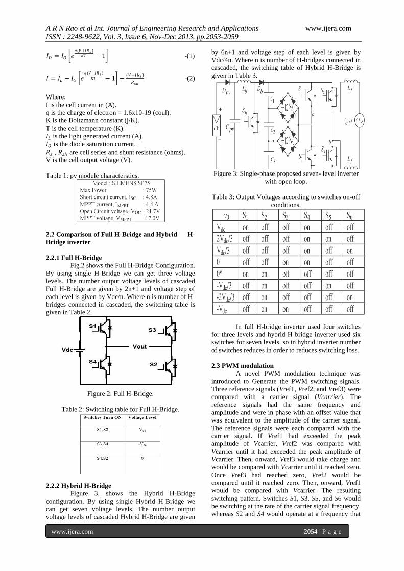
2.2.2 Hybrid H-Bridge
Figure 3, shows the Hybrid H-Bridge
configuration. By using single Hybrid H-Bridge we
can get seven voltage levels. The number output
voltage levels of cascaded Hybrid H-Bridge are given
by 6n+1 and voltage step of each level is given by
Vdc/4n. Where n is number of H-bridges connected in
cascaded, the switching table of Hybrid H-Bridge is
given in Table 3.
Figure 3: Single-phase proposed seven- level inverter
with open loop.
Table 3: Output Voltages according to switches on-off
conditions.
In full H-bridge inverter used four switches
for three levels and hybrid H-bridge inverter used six
switches for seven levels, so in hybrid inverter number
of switches reduces in order to reduces switching loss.
2.3 PWM modulation
A novel PWM modulation technique was
introduced to Generate the PWM switching signals.
Three reference signals (Vref1, Vref2, and Vref3) were
compared with a carrier signal (Vcarrier). The
reference signals had the same frequency and
amplitude and were in phase with an offset value that
was equivalent to the amplitude of the carrier signal.
The reference signals were each compared with the
carrier signal. If Vref1 had exceeded the peak
amplitude of Vcarrier, Vref2 was compared with
Vcarrier until it had exceeded the peak amplitude of
Vcarrier. Then, onward, Vref3 would take charge and
would be compared with Vcarrier until it reached zero.
Once Vref3 had reached zero, Vref2 would be
compared until it reached zero. Then, onward, Vref1
would be compared with Vcarrier. The resulting
switching pattern. Switches S1, S3, S5, and S6 would
be switching at the rate of the carrier signal frequency,
whereas S2 and S4 would operate at a frequency that

A R N Rao et al Int. Journal of Engineering Research and Applications www.ijera.com
ISSN : 2248-9622, Vol. 3, Issue 6, Nov-Dec 2013, pp.2053-2059
www.ijera.com 2055 | P a g e
was equivalent to the fundamental frequency. For one
cycle of the fundamental frequency, the proposed
inverter operated through six modes. The per unit
output-voltage signal for one cycle.
Figure 4: Seven-level output voltage (Vab) and
switching angles.
Figure 5: Seven-level inverter with closed-loop
control algorithm
2.4 control system
The control system comprises a MPPT
algorithm, a dc-bus voltage controller, reference-
current generation, and a current controller. The two
main tasks of the control system are maximization of
the energy transferred from the PV arrays to the grid,
and generation of a sinusoidal current with minimum
harmonic distortion, also under the presence of grid
voltage harmonics. The proposed inverter utilizes the
perturb-and-observe (P&O) algorithm for its wide
usage in MPPT owing to its simple structure and
requirement of only a few measured parameters. It
periodically perturbs (i.e., increment or decrement) the
array terminal voltage and compares the PV output
power with that of the previous perturbation cycle. If
the power was increasing, the perturbation would
continue in the same direction in the next cycle;
otherwise, the direction would be reversed. This
means that the array terminal voltage is perturbed
every MPPT cycle; therefore, when the MPP is
reached, the P&O algorithm will oscillate around it.
The P&O algorithm was implemented in the dc–dc
boost converter. The output of the MPPT is the duty-
cycle function. As the dc-link voltage Vdc was
controlled in the dc–ac seven level PWM inverter; the
change of the duty cycle changes the voltage at the
output of the PV panels. A PID controller was
implemented to keep the output voltage of the dc–dc
boost converter (Vdc) constant by comparing Vdc and
Vdc ref and feeding the error into the PID controller,
which subsequently tries to reduce the error. In this
way, the Vdc can be maintained.
Figure 6: Simulation of pwm switching sequence.
For Ma that is equal to, or less than, 0.33,
only the lower reference wave (Vref3) is compared
with the triangular carrier signal. The inverter’s
behaviour is similar to that of a conventional full-
bridge three-level PWM inverter. However, if Ma is
more than 0.33 and less than 0.66, only Vref2 and
Vref3 reference signals are compared with the
triangular carrier wave. The output voltage consists of
five dc-voltage levels. The modulation index is set to
be more than 0.66 for seven levels of output voltage to
be produced. Three reference signals have to be
compared with the triangular carrier signal to produce
switching signals for the switches.
Figure 7: Simulation circuit of Seven-level inverter
with closed-loop control algorithm
III. Single-Phase Proposed Inverter The proposed single-phase nine-level inverter
was developed from the five-level inverter in [12]. It
comprises a single-phase conventional H-bridge

A R N Rao et al Int. Journal of Engineering Research and Applications www.ijera.com
ISSN : 2248-9622, Vol. 3, Issue 6, Nov-Dec 2013, pp.2053-2059
www.ijera.com 2056 | P a g e
inverter, three bidirectional switches, and a capacitor
voltage divider formed by C, as shown in Figure. 8.
The modified H-bridge topology is significantly
advantageous over other topologies, i.e., less power
switch, power diodes, and less capacitor for inverters
of the same number of levels. Photovoltaic (PV)
arrays were connected to the inverter via a dc–dc
boost converter. The power generated by the inverter
is to be delivered to the power network, so the utility
grid, rather than a load, was used. The dc–dc boost
converter was required because the PV arrays had a
voltage that was lower than the three phase induction
motor rating.
Figure 8: Single-phase proposed Nine- level inverter
with open loop.
High dc bus voltages are necessary to ensure
that power flows from the PV arrays to electrical
machine. Proper switching of the inverter can produce
seven output-voltage levels (Vdc, 3Vdc/4, Vdc/2, Vdc/4,
0, -Vdc/4, -Vdc/2, -3Vdc/4, -Vdc) from the dc supply
voltage.
Table 4: Output Voltages according to switches on-off
conditions.
Zero output can be produced by two
switching combinations; switches S3 and S4 are ON,
or S1 andS2 are ON, and all other controlled switches
are OFF; terminal ab is a short circuit, and the voltage
applied to the load terminals is zero.
Figure 9: simulation circuit of Single-phase proposed
Nine- level inverter with open loop.
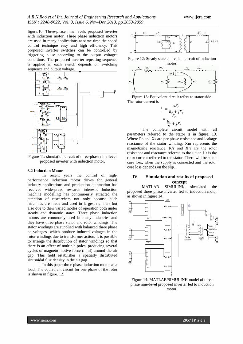
3.1 Proposed Three-Phase Nine-level Inverter with
Induction Motor
Figure 10: Three-phase nine level proposed inverter
with induction motor.
Three-phase proposed nine level inverter
connected in single phase of nine level inverters
electrically placed and operated by1200. As shown in
𝑉𝑂 𝑆1 𝑆2 𝑆3 𝑆4 𝑆5 𝑆6 𝑆7
𝑉𝑑𝑐 on off off on off off off
3𝑉𝑑𝑐
4
off off off on on off off
𝑉𝑑𝑐
2
off off off on off on off
𝑉𝑑𝑐
4
off off off on off off on
0 off off on on off off off
0∗ on on off off off off off
−𝑉𝑑𝑐
4
off on off off on off off
−𝑉𝑑𝑐
2
off on off off off on off
−3𝑉𝑑𝑐
4
off on off off off off on
−𝑉𝑑𝑐 off on on off off off off
A R N Rao et al Int. Journal of Engineering Research and Applications www.ijera.com
ISSN : 2248-9622, Vol. 3, Issue 6, Nov-Dec 2013, pp.2053-2059
www.ijera.com 2057 | P a g e
figure.10. Three-phase nine levels proposed inverter
with induction motor. Three phase induction motors
are used in many applications at same time the speed
control technique easy and high efficiency. This
proposed inverter switches can be controlled by
triggering pulse according to the output voltages
conditions. The proposed inverter repeating sequence
is applied in each switch depends on switching
sequence and output voltage.
Figure 11: simulation circuit of three-phase nine-level
proposed inverter with induction motor.
3.2 Induction Motor In recent years the control of high-
performance induction motor drives for general
industry applications and production automation has
received widespread research interests. Induction
machine modelling has continuously attracted the
attention of researchers not only because such
machines are made and used in largest numbers but
also due to their varied modes of operation both under
steady and dynamic states. Three phase induction
motors are commonly used in many industries and
they have three phase stator and rotor windings. The
stator windings are supplied with balanced three phase
ac voltages, which produce induced voltages in the
rotor windings due to transformer action. It is possible
to arrange the distribution of stator windings so that
there is an effect of multiple poles, producing several
cycles of magneto motive force (mmf) around the air
gap. This field establishes a spatially distributed
sinusoidal flux density in the air gap.
In this paper three phase induction motor as a
load. The equivalent circuit for one phase of the rotor
is shown in figure. 12.
Figure 12: Steady state equivalent circuit of induction
motor.
Figure 13: Equivalent circuit refers to stator side.
The rotor current is
𝐼𝑟 =𝑠𝐸𝑟
𝑅𝑟 + 𝑗𝑋𝑟
=𝐸𝑟
𝑅𝑟
𝑠+ 𝑗𝑋𝑟
The complete circuit model with all
parameters referred to the stator is in figure. 13.
Where Rs and Xs are per phase resistance and leakage
reactance of the stator winding. Xm represents the
magnetizing reactance. R’r and X’r are the rotor
resistance and reactance referred to the stator. I’r is the
rotor current referred to the stator. There will be stator
core loss, when the supply is connected and the rotor
core loss depends on the slip.
IV. Simulation and results of proposed
concept MATLAB SIMULINK simulated the
proposed three phase inverter fed to induction motor
as shown in figure 14.
Figure 14: MATLAB/SIMULINK model of three
phase nine-level proposed inverter fed to induction
motor.

A R N Rao et al Int. Journal of Engineering Research and Applications www.ijera.com
ISSN : 2248-9622, Vol. 3, Issue 6, Nov-Dec 2013, pp.2053-2059
www.ijera.com 2058 | P a g e
Figure 15: Switching pulses for nine-level inverter.
In proposed inverter before placed a boost
dc-dc converter operated with frequency 𝑓𝑏 =
10KHz.which is step up the output voltage of PV
panel up to 400V and PV output voltage is 50V. This
PV voltage depended on solar radiation which is
simulated as figure.1 each phase have separate PV
panel and boost dc-dc converter. Three phase
proposed nine inverter switching pulse per phase
shown in figure 17. Remaining two phase switching
control pulse operated with displacement of1200.
Figure 16: single-phase seven-level inverter output
voltage
Figure 17: Three-phase nine-level inverter (a) Output
Voltage, (b) Output Current.
Figure 18: Induction Motor (a) Rotor speed, (b)
Electromagnetic Torque.
Figure 19: Induction motor (a) Rotor current, (b) stator
current.
Figure 20: THD result for seven-levels of output
voltage

A R N Rao et al Int. Journal of Engineering Research and Applications www.ijera.com
ISSN : 2248-9622, Vol. 3, Issue 6, Nov-Dec 2013, pp.2053-2059
www.ijera.com 2059 | P a g e
Figure 21: THD result for nine-levels of output
voltage.
The THD measurement of Fig.19
corresponds to the waveform of Fig. 20, while the
THD measurements correspond to the waveforms of
respectively. Comparing all two THD measurements,
the nine-level inverter produced the lowest THD
compared with the seven-level inverter. This proves
that, as the level increases, the THD reduces.
Table5: total harmonic distortion different levels
Inverter level THD
Seven level 22.13%
Nine level 18.63%
Three phase nine-level inverter output voltage and
current as shown in figure 17. This proposed inverter
output applied to induction motor of rating is 400V,
50Hz, below 1500RPM, and load torque 10. Induction
motor results shown in figure 18 and 19, in figure 18
shown rotor speed 1460RPM and Electromagnetic
torque; in figure 19 shown rotor current and stator
current. Finally THD in circuit 18%, this proposed
topology is very high efficiency and economic.
V. Conclusion This paper presents a new three phase nine-
level inverter with reduced switches compare to
common multi level inverter. Multilevel inverters
offer improved output waveforms and lower THD. In
this topology less THD in the nine-level inverter
compared with that in the seven-level inverters is
connected PV inverters. This inverter provided to
induction motor with smooth output and better
voltage. Switching loss reduce in this topology than
the common three phase multi-level-inverter.
References [1] M. Calais and V. G. Agelidis, ―Multilevel
converters for single-phase grid connected
photovoltaic systems—An overview,‖ in Proc.
IEEE Int. Symp. Ind. Electron., 1998, vol. 1, pp.
224–229.
[2] S. B. Kjaer, J. K. Pedersen, and F. Blaabjerg,
―A review of single-phase grid connected
inverters for photovoltaic modules,‖ IEEE
Trans. Ind. Appl., vol. 41, no. 5, pp. 1292–1306,
Sep./Oct. 2005.
[3] P. K. Hinga, T. Ohnishi, and T. Suzuki, ―A new
PWM inverter for photovoltaic power
generation system,‖ in Conf. Rec. IEEE Power
Electron. Spec. Conf., 1994, pp. 391–395.
[4] Y. Cheng, C. Qian, M. L. Crow, S. Pekarek,
and S. Atcitty, ―A comparison of diode-
clamped and cascaded multilevel converters for
a STATCOM with energy storage,‖ IEEE
Trans. Ind. Electron., vol. 53, no. 5, pp. 1512–
1521, Oct. 2006.
[5] M. Saeedifard, R. Iravani, and J. Pou, ―A space
vector modulation strategy for a back-to-back
five-level HVDC converter system,‖ IEEE
Trans. Ind. Electron., vol. 56, no. 2, pp. 452–
466, Feb. 2009.
[6] S. Alepuz, S. Busquets-Monge, J. Bordonau, J.
A. M. Velasco, C. A. Silva, J. Pontt, and J.
Rodríguez, ―Control strategies based on
symmetrical components for grid-connected
converters under voltage dips,‖ IEEE Trans.
Ind. Electron., vol. 56, no. 6, pp. 2162–2173,
Jun. 2009.
[7] J. Rodríguez, J. S. Lai, and F. Z. Peng,
―Multilevel inverters: A survey of topologies,
controls, and applications,‖ IEEE Trans. Ind.
Electron., vol. 49, no. 4, pp. 724–738, Aug.
2002.
[8] J. Rodriguez, S. Bernet, B. Wu, J. O. Pontt, and
S. Kouro, ―Multilevel voltage-source-converter
topologies for industrial medium-voltage
drives,‖ IEEE Trans. Ind. Electron., vol. 54, no.
6, pp. 2930–2945, Dec. 2007.
[9] M. M. Renge and H. M. Suryawanshi, ―Five-
level diode clamped inverterto eliminate
common mode voltage and reduce dv/dt in
medium voltagerating induction motor drives,‖
IEEE Trans. Power Electron., vol. 23, no. 4, pp.
1598–1160, Jul. 2008.
[10] E. Ozdemir, S. Ozdemir, and L. M. Tolbert,
―Fundamental-frequencymodulatedsix-level
diode-clamped multilevel inverter for three-
phasestand-alone photovoltaic system,‖ IEEE
Trans. Ind. Electron., vol. 56, no. 11, pp. 4407–
4415, Nov. 2009.
[11] P. Lezana, R. Aguilera, and D. E. Quevedo,
―Model predictive controlof an asymmetric
flying capacitor converter,‖ IEEE Trans. Ind.
Electron., vol. 56, no. 6, pp. 1839–1846, Jun.
2009.
[12] G. Ceglia, V. Guzman, C. Sanchez, F. Ibanez, J.
Walter, and M. I. Gimanez, ―A new simplified
multilevel inverter topology for DC–AC
conversion,‖ IEEE Trans. Power Electron., vol.
21, no. 5, pp. 1311–1319, Sep. 2006.