thrust a: back-end processes - university of … annual... · thrust a: back-end processes ......
TRANSCRIPT

7
THRUST A: BACK-END PROCESSES Personnel: Thrust Leaders:
• Rafael Reif, Electrical Engineering and Computer Science, MIT • Ara Philipossian, Chemical and Environmental Engineering, UA
Other PIs:
• Duane Boning, Electrical Engineering and Computer Science, MIT • Toshiroh Doi, Chemical and Environmental Engineering, UA • Karen K. Gleason, Chemical Engineering, MIT • David Graves, Chemical Engineering, UC Berkeley • Srini Raghavan, Materials Science and Engineering, UA
Other Researchers:
• Tae Park, Electrical Engineering and Computer Science, MIT (Post-Doc) • Mikhail Sorokin, Group of Elementary Processes in Gas Discharges, Eindhoven
University of Technology • Yun Zhuang, Chemical and Environmental Engineering, UA
Graduate Students:
• Creighton Anderson, Materials Science and Engineering, UA • Hong Cai, Materials Science and Engineering, MIT • Thomas Casserly, Chemical Engineering, MIT • Kelvin Chan, Chemical Engineering, MIT • Leslie Charns, Chemical and Environmental Engineering, UA (graduated 12/03) • Darren DeNardis, Chemical and Environmental Engineering, UA • Cheng-Che Hsu, Chemical Engineering, UC-Berkeley • Kim Leung, Materials Science and Engineering, UA • Zhonglin Li, Chemical and Environmental Engineering, UA • Lateef Mustapha, Chemical and Environmental Engineering, UA (graduated 6/03) • Mark Nierode, Chemical Engineering, UC-Berkeley • Daniel Rosales-Yeomans, Chemical and Environmental, UA • April Ross, Chemical Engineering, MIT • Yasa Samporno, Chemical and Environmental, UA • Ajay Somani, Materials Science and Engineering, MIT • Jam Sorooshian, Chemical and Environmental Engineering, UA • Subu Tamilmani, Materials Science and Engineering, UA • Xiaolin Xie, Physics, MIT
Undergraduate Students: • Winston Benally, Dine College, Tsaile AZ/ Chemical and Environmental
Engineering, UA (Summer REU) • Kelly Brink, Chemical and Environmental Engineering, UA • David Flaherty, Chemical Engineering, UC-Berkeley

8
• Michael Kasper, Chemical Engineering, UC-Berkeley • Deanna King, Chemical and Environmental Engineering, UA • Timothy Murrell, Chemical Engineering, Oregon State University/Chemical
Environmental Engineering, UA (REU) • Chad Su, Chemical Engineering, Berkeley (graduated May 03) • Masano Sugiyama, Chemical and Environmental Engineering, UA • Juan Weaver, Chemical and Environmental Engineering, UA
Mentors and Industrial Collaborators: • Kenneth Aitchison, Novellus Systems • Charles Allgood, DuPont • Eb Andideh, Intel • Ashizawa, Hitachi Chemical • Kris Bahten, Rippey • Indrajit Banerjee, Intel • Len Boroucki, Intelligent Planar • Chris Borst, Texas Instruments • Ralph Brandes, Degussa • Wayne Bunker, Intel Corporation • Ritwik Chattarjee, Motorola • John Cheney, Fujimi • Chidi Chidambaram, Texas Instruments • Larry Curtis, Rippey • James Degraffenreid, STM • Laertis Economikos, IBM • Darrel Erb, AMD • Simon Fang, Texas Instruments • Furukawa, Fujikoshi Machinery • Doug Goetz, 3M • Josh Golden, Microbar, Inc. • Michael Goldstein, Intel • Brian Goolsby, Motorola, Inc • Barry Gotlinsky, Pall Corporation • Aaron Gower-Hall, Praesagus, Inc. • Alfred Grill, IBM • Andreas Gutsch, Degussa • Habiro, Hitachi Chemical • Mike Hartig, Motorola • Dale Hetherington, Sandia National Laboratories • Oscar Hsu, Freudenberg • Steve Hymes, Sematech • Koichiro Ichikawa, Fujikoshi Machinery • Katsuyoshi Ina, Fujimi • Katsura Ito, Showa Denko

9
• Jim Jewett, Intel • Bing Ji, Air Products • Andy Johnson, Air Products • Frank Kaufman, Cabot Microelectronics • John Kelly, Novellus • Takanori Kido, Showa Denko • Hyungjun Kim, Hynix Semiconductor • Masaharu Kinoshita, Rodel-Nitta • Karen Kirmse, Texas Instruments • Thomas Knothe, Degussa • Hiroyuki Kojima, Hitachi Limited • Avi Kornblit, Lucent Technologies (Bell Labs) • Isamu Koshiyama, Fujimi • Warren Lai, Lucent Technologies • Michael Lane, IBM • Jenna Latt, Advanced Micro Devices • Jeong-Gun Lee, Hynix Semiconductor • John T.C. Lee, Lucent Technologies (Bell Labs) • Paul Lefevre, Fujimi • Patrick Levy, Pall Corporation • Laura Losey, TI • Wolfgang Lortz, Degussa • Shawming Ma, Hewlett Packard • Vincent Manno, Tufts University • Alvaro Maury, Lucent Technologies • Andrew McKerrow, TI • Laura Mendicino, Motorola • Keiji Miyachi, Asahi Sunac • Michael Mocella, DuPont • Hiroyuki Morishima, Hitachi Chemical • Takashi Nishiguchi, Hitachi Limited • Larry Novak, Radian International • Okumu Ouma, Lucent Technologies • Tony Pan, Applied Materials • Jin-Goo Park, Hangyang University • Edward Paul, Stockton College • David Peters, Praxair • Bernhard Pogge, IBM • Chris Rogers, Tufts University • E. Todd Ryan, AMD • Hidetaka Sato, Hitachi Chemical • Keishi Seki, Fujimi • Hiroshi Shiho, JSR • Yoshitomo Shimazu, Showa Denko

10
• Greg Shinn, Texas Instruments • Robert Small, EKC Technology Inc. • Taber Smith, Praesagus, Inc. • Jerry Stefani, Texas Instruments • Terry Sparks, Motorola • Yoshiyuki Seike, Asahi Sunac • Robert Small, DuPont-EKC Electronic Technologies • Aaron Smith, National Semiconductor • David Stein, Sandia National Laboratories • Mineo Takaoka, Asahi Sunac • Horoyuki Takei, Hitachi Chemical • Halbert Tam, JSR • Ralph Taylor-Smith, Lucent Technologies • Jeremy A. Theil, HP • Robert Tomin, Sandia National Laboratories • Saied Tousi, Pall Corporation • Joshua Tower, Philips AMS • Nobuo Uotani, Showa Denko • Jean Vangsness, Freudenberg • Geoffrey Varga, Degussa • Victor Vartanian, Motorola, Inc • Peter Ventzek, Motorola, Inc • David White, Praesagus, Inc. • Walter Worth, SEMATECH • Qingguo Wu, Novellus • Kai Yang, AMD • Larry Zazzera, 3M
Vision and Goals:
As the complexity of interconnects continues to increase, so does the number of process steps involved in the back-end-of-the-line. As a result, ESH concerns in this area continue to become more prominent. It is the goal of the investigators in Thrust A to develop technological solutions that address these issues. State of the Art:
Major ESH issues currently facing the semiconductor industry in the back-end-of-the-line include:
• Among the ESH issues currently facing the semiconductor industry in the back-end area are: the use and emission of perfluorocompounds (PFCs) from dielectric wafer etch and PECVD chamber clean processes, environmental issues associated with slurry waste from CMP processes, as well as the need for a low-k dielectric technology that results in environmentally benign process effluents.
• Planarization processes use large quantities of slurries and have low slurry utilization efficiencies; the effect of slurry flow rate and novel pad surfaces textures on the thermal, kinetic and tribological attributes of the process are not well understood.

11
• Pad life continues to be low for typical planarization processes; this impacts tool availability thus increasing capital costs
• The effect of temperature on copper and ILD removal rate is not well understood; as a results current removal rate models do not address the inherent non-isothermal conditions encountered in planarization processes
• Comprehensive evaluation and fundamental characterization of a new class of CMP pads (nonporous polymeric pads with embedded water soluble particles) is lacking
• The industry is moving to low shear force planarization processes in order to alleviate the integration issues associated with ULK dielectric de-lamination; methodologies (and associated fundamental knowledge) which help reduce shear force during planarization without compromising process performance are needed.
• Electroplating and CMP steps are currently separated in IC manufacturing. During Cu electroplating, with the added chemistries in the plating solution, the concentrations of the accelerators on the bottom of the trenches and the suppressors on the raised regions vary with different patterns, resulting in different deposition rates and non-uniform topography. This leaves a serious burden on the subsequent CMP process, as the initial non-uniform topography causes different polishing rates and cleaning times for different regions on the die.
• The extent of shear forces during post-CMP PVA brush scrubbing is not well understood, and the contribution of the PVA material and its geometric and physical characteristics on shear force are unclear. This has often placed a large burden on tool manufacturers and cleaning chemical suppliers to remove contaminants from wafer surfaces following planarization.
ESH Significance:
• Task A1 addresses the PFC issues via the development of replacement etch chemistries. It also focuses on predictive modeling of emissions from etching. This will provide in-depth understanding of PFC plasma etch processes and will help industry in optimizing for process and ESH goals.
• The goal of Task A2 is to meet an emerging technology need (low-k materials for intermetal dielectric applications) with built-in design for ESH. Task A3 primarily focuses on effluent studies of plasma in order to optimize for ESH goals.
• Task A3 and A1 will be working in collaboration for making reliable effluent models. The current Task A3 replaces the former PFC abatement task that was completed in 2000.
• The goal of Task A-4 is to minimize CMP waste through modeling of pattern dependency effects as well as through fundamental study of process tribology and fluid dynamics
• Task A-5 addresses fundamental pad characterization and modeling. Goals of this project are to develop and fully characterize existing and novel pads ‘tuned’ for specific tribological and fluid dynamics attributes for various CMP applications. This approach will allow pad manufacturers to identify and control critical pad parameters for reduced variability, longer pad life and improved planarization performance. The types of pads investigated in this study fall into two broad categories of (1) porous polyurethane closed-cell foam pads with novel surface textures, and (2) non-porous pads containing water-soluble particles.

12
• Task A-6 deals collectively with alternative planarization technologies such as integrated planarization and electroplating/electropolishing, fixed abrasive pads, and abrasive free slurries with emphasis on copper polish. The task also addresses a novel planarization method termed ‘controlled atmosphere polishing’ or CAP, which involves use of controlled polishing environments and chamber pressures for enhanced material removal and reduced chemical usage.
• Task A-7 focuses on quantifying the extent of frictional forces during post-planarization PVA brush cleaning as a function of brush kinematics, brush nodule design, cleaning solution pH, wafer pattern densities and applied brush pressure.
Accomplishments:
• Continued evaluation of other isomers of C4F6 for oxide etching on AME 5000 medium-density tool at MIT’s Microsystems Technology Laboratories.
• Statistically modeled effluents from existing database of PFC plasma oxide etch. • Empirically modeled effluents with 90% or more confidence by DOE. • Established differences between three isomers of C4F6, as their effluents and plasma
chemistry are different in medium density chamber. • The mechanical properties of the OSG dielectric material were improved and
controlled through adjusting processing conditions and enhanced by reactions between proximal end groups during annealing
• CVD dielectric materials with nano-scale porosity were created using polystyrene beads as the sacrificial porogen
• Single level air gap structures were fabricated using HFCVD deposited polyoxymethylene as the sacrificial material.
• Clarified the importance of inlet gases chemistry to effluent species composition and wall deposition rate for low k dielectric film (SiCN) etching.
• Measured neutral species densities and identified effluent species in Ar/C4F8 discharge.
• Made material balance for carbon and fluorine in Ar/C4F8 discharges. • Development of chip-scale models for shallow trench isolation (STI) CMP processes • Experiments and models for reduced dishing and erosion in advanced copper CMP
processes • New physically-motivated model for chip-scale prediction of copper electroplating
topography • Copper discs were shown to be viable and more economically feasible and
environmentally friendly replacements for copper deposited wafers for preliminary copper screening tests.
• Developed and validated 2-dimensional thermal model for oxide and copper CMP • Developed and validated a removal rate model for copper CMP based on a modified
Langmuir-Hinshelwood kinetics model • Determined the effect of copper slurry flow rate on thermal, tribological and kinetics
attributes pf the process. • Demonstrated the feasibility of ILD slurry filtration and regeneration

13
• Determined the tribological and kinetic attributed of cerium oxide-based slurries for ILD and STI applications. These slurries were shown to reduce solids content by a factor of 20.
• Developed a method to establish the envelope pressure during STI CMP for wafers of varying pattern density
• Determined the effect of novel groove designs on the tribology and kinetics of ILD CMP and identified a new design that significantly reduces slurry use without compromising frictional forces and removal rate.
• Completed mechanical, tribological, thermal and kinetic evaluation of non-porous pads containing water soluble particles and identified key pad properties needed for optimum CMP performance
• Elucidated the effect of oxidizer and solution pH on the removal rate and particle generation in copper CMP process using fixed abrasive pads.
• Identified a benign corrosion inhibitor for copper CMP process, which has performance characteristics comparable to BTA in certain chemistries
• Designed a novel method to directly measure the galvanic current and potential between copper and barrier metal during polishing conditions and measured the galvanic current and potential of copper –tantalum couple in various chemical systems during abrasion.
• Modified, installed and qualified new controlled atmosphere CMP tool capable of high (10 ATM) and low (0.5 ATM) chamber pressure processing under controlled gaseous ambient
• Obtained preliminary copper CMP kinetics data at low and moderate ambient pressures under nitrogen, air and oxygen environments with Fujimi’s PL-7102 slurry.
• Installed and qualified a high pressure micro-jet conditioning system and performed preliminary experiments comparing the HPMJ technology with conventional diamond conditioning.
• Characterized the tribological attributes of post-CMP PVA brush scrubbing on STI patterned wafers. Also, established the differences in the frictional forces when noduled brush rollers were used instead of flat brush rollers.
Industrial Interactions and Technology Transfer:
• Collaborating with International Sematech on low-k etching (Reif). • Visit to Applied Materials in August and to present current research (Reif). • Visits to Gleason lab at MIT and participation of industrial mentors Todd Ryan
(AMD) and Eb Andideh (Intel) in the weekly ERC teleconference. • Ross visits Texas Instruments (Dallas, TX) to discuss research and industry outlook. • Collaborated with Qingguo Wu (Novellus) to obtain hardness measurements using
nano-indentation. • Discussed collaboration for porous low-k metrology using spectroscopic ellipsometry
with SOPRA (Gleason). • Teleconference presentation on OSG materials to Applied Materials (Gleason). • Discussions on air dielectric technology with Michael Lane, IBM; Sameer Ajmera,
TI; and Sadasivan Shankar, Intel at SRC BEP TAB held at RPI, Troy NY, Oct. 2003.
14
• PI and graduate students visited Motorola (Austin, TX) to report results and plan joint research.
• Conducted teleconference every other week with Motorola mentors regarding project progress.
• Shared experimental result with Motorola. • Air Products donated gases for research. • Design and characterization of new slurry recycling and regeneration system for ILD
CMP applications was performed jointly by Pall Corporation, Fujimi Corporation an The University of Arizona (Philipossian).
• Donation of gas cabinet and continuous supply of inert and reactive gases for the Controlled Atmosphere Polishing (CAP) process by Praxair (Philipossian and Doi).
• Collaboration with Rodel-Nitta on new pad grove designs for improved frictional and slurry flow characteristics (Philipossian and Doi).
• Collaboration and student exchange (Leslie Charns for 4 months) with Tufts University on developing methodologies for spectral analysis of raw frictional; data essential for quantifying the extent of stick-slip phenomena during CMP (Philipossian).
• Collaboration with Intelligent Planar for development of thermal models for ILD and copper processes as well as kinetics modeling of copper CMP processes (Philipossian).
• Joint research between MIT, Sandia National Laboratories and The University of Arizona on optimized endpoint detection schemes and models resulting in reduced slurry consumption ((Philipossian and Boning).
• Qualification of two Fujikoshi polishers at The University of Arizona for CAP and 200-mm tribology projects (Philipossian and Doi).
• Collaboration with Freudenberg, Sandia National Laboratories and The University of Arizona on FX-9 mechanical and kinetic pad characterization for ILD and copper applications (Philipossian).
• Qualification of two Asahi Sunac High Pressure Micro-Jet systems (100-mm and 200-mm systems) to act as replacements for diamond disc conditioner (Philipossian)
• Collaboration with Fujikoshi for re-design of new wafer polishing head for the CAP tool (Philipossian)
• Collaboration with Showa Denko on characterization of their new cerium oxide slurry for ILD and STI applications (Philipossian).
• Collaboration with STM on colloidal silica slurry flow rate reduction and its impact on pad life and thermal and kinetic attributes of ILD CMP (Philipossian).
• Worked with EKC technology in characterizing the fate of hydroxylamine based compounds used in copper CMP (Raghavan)
• Texas Instruments (C. Chidambaram, C. Borst, G. Shinn) – collaboration on development of copper plating and copper CMP pattern dependent model (Boning)
• Praesagus, Inc. (T. Smith, D. White, A. Gower-Hall) – licensing and development of chip-level copper CMP test patterns and models, and measurements of plated and polished copper wafers (Boning)
• Hynix Semiconductor (J.-G. Lee, H. Kim) – interaction to obtain copper plating and multi-level copper CMP experimental results using MIT test masks (Boning)

15
• National Semiconductor (A. Smith) – experiments to study STI CMP pattern effects. Student Xiaolin Xie had a summer internship at South Portland, Maine to execute STI CMP experiments and measurements (Boning)
• Philips AMS (J. Tower) – measurements of copper field thickness. • Neopad, Inc. (PK Roy) – discussions and planning of research interaction on pattern
effects in novel CMP pads, leading to Neopad joining the ERC (Boning and Philipossian)
Strategic Plan: Next-Year Plans:
• Study plasma etching in order to develop predictive models for PFC plasma etching of dielectrics.
• Generate effluent models using well-stirred plasma reactor approximation. • Investigate the use of OES (as addition to FTIR) for PFC emissions characterization. • Use FTIR, NMR and nano-indentation to characterize the fundamental relationship
between material hardness and structure of the OSG matrix. • Demonstrate a single step process for porous OSG deposition to simultaneously
deposit polystyrene beads (15nm to 100nm diameter) and matrix material to control degree of porosity, ranging from 10-50%, using the newly established CVD reactor configuration.
• Explore cyclodextrin as porogen candidate for porous OSG CVD. • Create micro-scale air gap formations using lithography for patterning. • Develop fundamental model for of air gap formation. • Fluorocarbon-based plasma neutral species measurement under different conditions
and chemistries. • Further investigate global warming gases formation mechanism for etching low K
dielectric films. • Correlation between CF4/C2F6 formation and specific neutral species density. • Determine whether the ‘universal’ relationship between removal rate and COF
applies to copper polishing as well as ILDF polishing with colloidal silica slurries. • Explore the utility of the ‘interfacial interaction index’ on copper and ILD polish
applications. • Develop second generation thermal model to aide in improved kinetics analysis of
ILD and copper processes and extend the model to industrial-scale polishers. • Fully explore (both experimentally and through simulation) the effect of slurry flow
rate on copper polish. • Complete work on de-coupling of the chemical and mechanical attributes of CMP
through controlled removal rate vs. temperature experiments (ILD and copper). • Determine the effect of novel pad grooving on copper and ILD polish on 200-mm
platform. • Complete DMA and TMA characterization of various types of pads and determine the
extent of their effect on COF, thermal transients and removal rate for ILD and copper CMP processes.
• Wrap up the work on copper removal with fixed abrasive pad.

16
• Focus on developing abrasive free chemistries for polishing copper and tantalum nitride films using conventional pads.
• Study galvanic corrosion between copper and tantalum nitride at different area ratios in the developed abrasive free chemistries.
• Analyze experimental data from a new STI CMP test mask, gathered in collaboration with National Semiconductor, and extend CMP model as necessary to account for rectangular as opposed to long line features.
• Develop a model relating wafer surface pattern evolution to motor current-based endpoint detection signals, in order to optimize detection for different wafer layouts.
• Extend model to accommodate electroplated thickness (or time) as a parameter. • Investigate plating pattern dependencies in multilevel copper structures (current
model assumes the starting surface is flat, as in metal 1, only). • Complete validation of the new copper CMP model against dishing and erosion data. • Implement extensions to the copper CMP model for multilevel effects (e.g. metal 2
and above), and test against conventional copper CMP data. • Integrate AFP/non-Prestonian model extensions into multilevel copper model. The
goal is to be able to show not only dishing and erosion results, but also to predict regions on the chip which may have difficulty in clearing the copper completely.
• Simulation studies to formulate what an “optimal” rate vs. pressure slurry curve would look like, in order to achieve the best patterned wafer performance.
• Study the effect of PVA brush properties (i.e. porosity, hardness and toughness) on COF and system tribology.
• Conduct Fourier transform spectral analysis to determine whether variance analysis of the raw frictional data can shed light on the actual mechanism of wafer scrubbing.
• Perform these experiments with a variety of cleaning solutions and brush properties. Long-Term Plans:
• Provide better understanding of role of plasma constituents to serve as a tool in designing and optimizing high performance etch processes.
• Development of user-friendly models and computer simulations of plasma tool design and optimization for ESH-objectives. (in collaboration with Task A-3).
• Establish fundamental structure-property-processing relationships required for integrating porous, low-k materials and air dielectrics into manufacturing steps thereby reducing the number of metallization layers and environmental impact.
• Construction of reliable effluent model that can predict effluent composition. (in collaboration with Task A-1).
• Develop fundamental models relating process tribology to pad life. • Develop fundamental models relating removal rate, COF, lubrication mechanism,
particle morphology and process temperature to one another. • Develop prototype for ILD slurry filtration and regeneration. • Propose and validate a pad design with improved ESH and process characteristics. • Apply the chemical and electrochemical knowledge gained to the development of
planarization techniques which simultaneously use mechanical and electrochemical factors for planarization.
17
• Develop and transfer a methodology and model for chip-scale prediction and optimization of dishing and erosion performance in advanced CMP processes.
• Develop optimization methods for coupled plating/CMP process optimization that minimize process thickness, process time, and consumable usage.
• Investigate pattern and layout dependent models for electropolishing, simultaneous deposition and planarization of copper, or other alternative processes.
• Understand the mechanisms behind AFP patterned wafer behavior, and propose alternative slurry/pad behaviors that would combine both good pattern planarization and environmental friendliness.
• Contribute to basic understanding of wafer scrubbing by de-coupling the two widely held mechanisms of capillary suction and brush-wafer abrasion by performing coefficient of friction tests using brush rollers having vastly different porosities.
• Develop physically and chemically based models relating the effect of brush properties on COF and relate the models to recommend improvements to current PVA brush roller designs.
• Develop a model to predict brush life and efficiency to key brush and process attributes and define a cleaning process compatible with next generation ICs.
Facilities:
• MIT’s Microsystems Technology Laboratories (contains Applied Materials Precision 5000 etch tool, Applied Materials Centura 5300 HDP etch tool, and Novellus Concept One PECVD tool).
• MIT’s Center for Materials Science and Engineering (possesses analytical equipment such as Auger electron spectroscopy instrument).
• New reactor design to accommodate simultaneous deposition of porogen particles with organosilicate dielectric matrix material.
• State-of-the-art thin film characterization laboratory. • CVD Reactor for sacrificial layer depositions utilized for air gap fabrication. • The UC Berkeley lab focuses on plasma processing-related diagnostics and modeling.
An inductively coupled research plasma reactor was built and tested. Several plasma diagnostics, including optical emission spectroscopy, mass spectrometry, and Langmuir probe are utilized. Computer modeling of the plasma reactor is also done at UC Berkeley on several desktop workstations.
• Nanospec for low-k dielectric film thickness measurement. • UA Microelectronics Laboratory
- One Speedfam-IPEC 372M polisher capable of handling 150-mm wafers - One Speedfam-IPEC 372M polisher capable of handling 200-mm wafers
(Philipossian) - Lam DSS-200 double-sided PVA brush scrubber (Philipossian) - KLA-Tencor SS7600 defect inspection tool (Philipossian) - KLA-Tencor SS6200 defect inspection tool
• UA Innovative Planarization Laboratory - New 200-mm polisher and tribometer manufactured jointly by Fujikoshi and
The University of Arizona, featuring an Ebara polishing head, used for

18
planarization, frictional analysis, thermography and fluid dynamics analysis of ILD and metal films (Philipossian)
- Fujikoshi 100-mm controlled atmosphere polisher (CAP) equipped with a variety of reactive and inert gases capable of processes with gauge pressures ranging from 0.5 to 5 atmosphere (Philipossian)
- Three table-top polishers and tribometers (100-mm wafers) for planarization, frictional analysis, thermography and fluid dynamics analysis of ILD and metal films (Philipossian)
- Novel 100-mm PVA brush scrubber and tribometer for post-CMP cleaning and frictional analysis (Philipossian)
- TA Instruments DSC-100, DMA-2980 and TMA-2940 for pad thermal-mechanical characterization (Philipossian)
- Tekscan Pressure Sensor for real-time pressure mapping for CMP and post-CMP cleaning applications (Philipossian)
- Veeco Dektak 3ST profilometer (Philipossian) - TA Instruments AR550 slurry rheometer (Philipossian) - Gaertner LSE-WS 200-mm Ellipsometer (Philipossian) - New proprietary optical device (manufactured by Hitachi Limited) for real-
time measurement of pad asperity collapse during polishing (Philipossian) - Two Asahi Sunac high pressure micro-jet systems (100-mm and 200-mm)
used as alternate methods to conventional diamond discs for pad conditioning (Philipossian)
- Pall ILD slurry filtration and regeneration system capable of supporting four large-scale polishers (Philipossian)
- Laboratory scale polishing tool which enables in situ electrochemical measurements of interest to metal CMP (Raghavan)
• MIT Microsystems Technology Laboratory (planarization-related facilities) - Strasbaugh 6EC CMP tool for dielectric applications - Strasbaugh 6EG CMP tool installed for copper applications - Metrology equipment including P10 profilometer, UV1250 and SM-300 thin
film thickness measurement tools from KLA-Tencor - FLIR Systems Agema 550 infrared thermal imaging system (on loan to UA)
Publications, Presentations and Patents: Task A-1: Publications:
• V. Vartanian, B. Goolsby, R. Chatterjee, R. Kachmarik, D. Babbitt, R. Reif, E. Tonnis, D. Graves, “Reduction of Semiconductor Process Emission by Reactive Gas Optimization”, submitted to IEEE Transaction on Semiconductor Manufacturing.
Presentations:
• Somani A., “Modeling of Effluents”, Applied Materials, Santa Clara, 08/19/03. Task A-2: Presentations:
19
• Gleason, K.K., “Engineering the Chemistry of Vapor Deposition”, 3M, Minneapolis, MN, 1/16/03. invited
• Gleason, KK, “Engineering the Chemistry of Vapor Deposition”, Plasma Technology Network Seminar, Universite du Quebec, 4/11/03. invited
• Gleason, KK, “Engineering the Chemistry of Vapor Deposition”, Chemical Engineering Department Seminar, UCLA, 4/18/03. invited
• Ross AD, “Chemical Vapor Deposition of Organosilicon Composite Materials for Porous Low-k Dielectrics”, Materials Research Society Spring Meeting, San Francisco, CA, 04/24/03.
• Casserly TB, “Selection of an Overlying Dielectric and Sacrificial Material for Air Gap Fabrication”, Materials Research Society Spring Meeting, San Francisco, CA, 04/24/03.
• Gleason, KK, “Air Dielectric Fabrication via CVD Sacrificial Layers, Materials Research Society Spring Meeting, San Francisco, CA, 04/24/03. invited by Jim Leu, Intel
• Gleason, KK, “CVD Organosilicon Low k Materials”, Applied Materials teleconference, 6/3/03.
• Gleason, KK, “Two PECVD Approaches for Porous Organosilicate Glass (OSG) Low k Dielectrics”, 16th International Symposium on Plasma Chemistry, Taormina, Italy, 6/23/03.
• Casserly TB, “Selection of an Overlying Dielectric and Sacrificial Material for Air Gap Fabrication”, Techcon, Dallas, TX, 08/25/03.
• Chan K, “Chemical Vapor Deposition of Polyoxymethylene as a Sacrificial Layer for Air-Gap Fabrication,” SRC TECHCON, Dallas, TX, 08/25/03.
• Gleason, KK, “ Nanocoatings by Hot Filament Chemical Vapor Deposition”, Polymer Processing Science and Technology Seminar, MIT, Cambridge, MA, 10/1/03.
• Gleason, KK, “Air Dielectric: CVD Sacrificial Materials & Modeling”, SRC BEP TAB, RPI, Troy, NY, 10/8/03. invited by Harold Hosack
• Chan K, “Thin Polyoxymethylene Film as a Sacrificial Material for Air-Gap Fabrication,” AIChE Annual Meeting, San Francisco, CA, 11/18/03
• Ross AD, “Chemical Vapor Deposition of Organosilicon Composite Materials for Porous Low-k Dielectrics”, Techcon, Dallas, TX, 08/25/03.
• Ross AD, “Chemical Vapor Deposition of Organosilicon Composite Materials for Porous Low-k Dielectrics”, Texas Instruments, Dallas, TX, 08/28/03.
• Casserly TB, “Selection of an Overlying Dielectric and Sacrificial Material for Air Gap Fabrications: Modeling Air Gap formation”, MIT Departmental Seminar, Cambridge, MA, 12/01/03.
• Chan K, “Chemical Vapor Deposition of Polyoxymethylene as a Sacrificial Layer for Air-Gap Fabrication,” MIT Chemical Engineering Departmental Seminar Series, Cambridge, MA, 12/01/03.
• Chan K, “Chemical Vapor Deposition of Polyoxymethylene as a Sacrificial Layer for Air-Gap Fabrication,” MRS Fall Meeting, Boston, MA, 12/03/03.
• Gleason, KK, “Nanocoatings by Chemical Vapor Deposition”, Honeywell Briefing, MIT, Cambridge, MA, 12/10/03.
20
Patents and Disclosures: • Gleason KK., Wu, Q., and Ross, AD. “Porous Material Formation By Chemical
Vapor Deposition Onto Colloidal Crystal Templates,” US Patent Application Serial NO. 10.624,959
Task A-3: Publications:
• M. T. Radtke, J. W. Coburn, and David B. Graves, "C4F8 dissociation in an inductively coupled plasma," J. Vac. Sci. Technol. A 21 (4), 1038 (2003).
Task A-4: Publications:
• White, D., J. Melvin, and D. Boning, “Characterization and Dynamic Modeling of Thermal Behavior in Chemical Mechanical Polishing (CMP),” Journal of the Electrochemical Society, vol. 150, no. 4, pp. G271-G278, April 2003.
• A. Philipossian and S. Olsen, “Fundamental Tribological and Removal Rate Studies of Inter-Layer Dielectric CMP”, Jpn. J. Appl. Phys. 42 (10), 6371 (2003).
• D. DeNardis, J. Sorooshian, M. Habiro, C. Rogers and A. Philipossian, “Tribology and Removal Rate Characteristics of Abrasive-Free Slurries for Copper CMP Applications”, Jpn. J. Appl. Phys. 42 (11), 6809 (2003).
• A. Philipossian and E. Mitchell, “.Dispersion Number Studies in Chemical Mechanical Planarization”, Journal of The Electrochemical Society, 150 (12), 854 (2003).
• A. Philipossian and E. Mitchell, "Slurry Utilization Efficiency Studies in CMP", Jpn. J. Appl. Phys. 42 (12), 7259 (2003).
Presentations:
• Xie, X., T. Park, Brian Lee, T. Tugbawa, H. Cai and D. Boning, “Re-examining the Physical Basis of Planarization Length in Pattern Density CMP Models,” MRS Spring Meeting, Symposium F: Chemical Mechanical Planarization, San Francisco, CA, April 2003.
• Park, T., T. Tugbawa, H. Cai, X. Xie, D. Boning, C. Chidambaram, C. Borst, and G. Shinn, “Integrated Chip-Scale Prediction of Copper Interconnect Topography,” MRS Spring Meeting, Symposium F: Chemical Mechanical Planarization, San Francisco, CA, April 2003.
• Xie, X., and D. Boning, “Integrated Modeling of Nanotopography Impact in Patterned STI CMP,” Chemical-Mechanical Planarization for ULSI Multilevel Interconnect Conference, Marina Beach, CA, Feb. 2003.
• Boning, D., “Pattern Dependent Characterization of Copper Interconnect,” Tutorial, International Conference on Microelectronic Test Structures (ICMTS), Monterey CA, March 2003.
• Boning, D., “Pattern Dependencies in Copper Electroplating and CMP,” The Planarization & CMP Technical Meeting 2003, Japan Society of Precision Engineering, San Francisco, CA, July 2003.

21
• D. Boning, "Spatial Uniformity as a Key Challenge in Semiconductor Process Control," AVS 50th International Symposium, Manufacturing Science and Technology, Baltimore, MD, Nov. 2003.
• D. King and A. Philipossian, “Friction and Removal Rate Studies of ILD CMP Using Novel Cerium Oxide Slurries”, 8th International Symposium on Chemical Mechanical Planarization, Lake Placid, New York (2003).
• M. Sugiyama, D. King, L. Charns, J. Degraffenreid, H. Nguyen-Ngoc, and A. Philipossian, “Tribological and Removal Rate Characterization of Colloidal vs. Fumed Silica Slurries in ILD CMP’, Abstract 927, 204th Meeting of Electrochemical Society, Orlando, FL (2003).
• P. Levy, S. Rader, P. Lefevre, K. Ina, F. Shadman, M. Sugiyama, and A. Philipossian, “Analytical and Functional Characterization of Recycled Fumed Silica Slurries in ILD CMP’, Abstract 928, 204th Meeting of Electrochemical Society, Orlando, FL (2003).
• Z. Li, L. Borucki, and A. Philipossian, “Determining the Effect of Slurry Flow Rate on the Tribological, Thermal and Removal Rate Attributes of Copper CMP”, Abstract 909, 204th Meeting of Electrochemical Society, Orlando, FL (2003).
• Z. Li, K. Ina, P. Lefevre, and A. Philipossian, “Determining the Effect of Slurry Surfactant, Abrasive Size and Content on the Tribology and Kinetics of Copper CMP”, Abstract 908, 204th Meeting of Electrochemical Society, Orlando, FL (2003).
• D. Rosales-Yeomans, T. Doy, and A. Philipossian, “The Spectral Fingerprints and The Sounds of CMP”, Abstract 924, 204th Meeting of Electrochemical Society, Orlando, FL (2003).
• A. Philipossian, D. Rosales-Yeomans, M. Kinoshita and T. Doi, Recent Advances in ILD & Copper CMP Research at The University of Arizona, Invited presentation at the 35th meeting of the Japan Society of Precision Engineers; CMP Special Committee, Tokyo, Japan (2003).
• A. Philipossian, Overview of the Engineering Research Center for Environmentally Benign Semiconductor Manufacturing and CMP Activities at the University of Arizona, Invited presentations at the 145th meeting of the Japan Society for Promotion of Science, Tokyo, Japan (2003).
• Z. Li, S. Rader, P. Lefevre, K. Ina, and A. Philipossian, “Comparison of Copper Disc and Copper Wafer Polishing Processes in Terms of Their Kinetic, Tribological and Thermal Characteristics”, Abstract 899, 204th Meeting of Electrochemical Society, Orlando, FL (2003).
• R. Brandes, T. Knothe, F. Klaessig, F. Menzel, W. Lortz, G. Varga, T. Shibasaki and A. Philipossian, “Metal Doped Silica Abrasive Slurries and Their Effect on Friction and Removal Rate Characteristics of ILD and STI CMP”, 8th International Chemical-Mechanical Polish for ULSI Multilevel Interconnection Conference, Marina Del Ray, CA (2003).
Patents and Disclosures:
• Philipossian, A., UA, Sorooshian, J., UA, Goldstein, M., Intel, Gutsch, A., Degussa AG. - Conventional polishing platen with an integrated magnetic track for enhanced polishing and slurry control. (PAF, UA03-101, 4/2003)
22
• Philipossian, A., UA, Sorooshian, J., UA, Goldstein, M., Intel. Conventional polishing platen and carrier head indicating the location of an integrated magnetic layout. (PAF, UA03-100, 4/2003)
• Philipossian, A., UA, Sorooshian, J., UA. Conventional polishing platen and carrier head with an integrated electrical source for enhanced polishing. (PAF, UA03-099, 3/2003)
• Philipossian, A., UA, Rosales-Yeomans, D., UA, Charns, L., UA. A novel method employing spectral analysis of real-time friction data is used to investigate the soft and porous copper complex layer that is known to play an integral part in abrasive-free copper chemical-mechanical planarization (CMP). (PAF, UA03-102, 2/2003)
• Philipossian, A., UA, DeNardis, D., UA, Rosales-Yeomans, D., UA, Charns, L., UA. A novel tool diagnostic for chemical mechanical planarization (CMP) equipment using Fourier transform spectral analysis. (PAF, UA03-098, 2/2003)
Task A-5: Publications:
• J. Sorooshian, A. Philipossian, M. Goldstein, S. Beaudoin, and W. Huber, “Impact of Wafer Geometry and Thermal History on Pressure and von Mises Stress Non-Uniformity During Chemical Mechanical Planarization”, Jpn. J. Appl. Phys. 42 (10), 6363 (2003).
Presentations:
• L. Charns, M. Sugiyama and A. Philipossian, “Thermal and Mechanical Properties of CMP Pads Containing Embedded Water Soluble Particles”, 8th International Symposium on Chemical Mechanical Planarization, Lake Placid, New York (2003).
• J. Cornely, C. Rogers, V. Manno and A. Philipossian, “ In Situ Temperature Measurement During Oxide Chemical Mechanical Planarization”, Materials Research Society Symposium Proceeding, Vol. 767, p.33, San Francisco, CA (2003).
• L. Borucki, L. Charns and A. Philipossian, “Analysis of Frictional Heating of Grooved and Flat CMP Polishing Pad”, Abstract 918, 204th Meeting of Electrochemical Society, Orlando, FL (2003).
• D. Rosales-Yeomans, T. Doy, M. Kinoshita, and A. Philipossian, “Effect of Novel pad Texture Designs on Tribology and Removal Rate Characteristics of ILD CMP”, Abstract 917, 204th Meeting of Electrochemical Society, Orlando, FL (2003).
• L. Borucki, Z. Li, and A. Philipossian, “Heating and Convection in Copper Polishing”, Abstract 907, 204th Meeting of Electrochemical Society, Orlando, FL (2003).
• A. Philipossian and E. Mitchell, “Slurry Utilization Efficiency Studies in Chemical Mechanical Planarization”, Materials Research Society Symposium Proceedings, Vol. 767, p.21, San Francisco, CA (2003).
• A. Philipossian and S. Olsen, “Effect of Pad Surface Texture and Slurry Abrasive Concentration on Tribological and Kinetic Attributes of ILD CMP”, Materials Research Society Symposium Proceedings, Vol. 767, p.119, San Francisco, CA (2003).

23
Task A-6: Publications:
• W. Huang, S. Tamilmani, S. Raghavan and R. Small, “Dissolution of Copper Thin Films in Hydroxylamine-based Solutions”, International Journal of Mineral Processing, Vol. 72, p. 365– 372 (2003).
• S. Raghavan, S. Tamilmani, W. Huang and R. small, “Corrosion Issues in Chemical Mechanical Planarization of Copper”, Proceedings of The Eighth International Chemical Mechanical Planarization For ULSI Multilevel Interconnection Conference, p. 246-256, Feb 2003.
Presentations:
• S. Raghavan, “Advances in Planarization Science and Technology”, Presentation made in Taiwan at a conference organized by ITRI, October 28, 2003
Task A-7: Publications:
• Philipossian and L. Mustapha, “Effect of Tool Kinematics, Brush Pressure and Cleaning Fluid pH on Coefficient of Friction and Tribology of Post-CMP PVA Brush Scrubbing Processes”, Materials Research Society Symposium Proceedings, Vol. 767, p.217, San Francisco, CA (2003).

24
DETAILS OF TASKS AND SUBTASKS OF THRUST A Task A-1: PFC Alternatives Personnel: PI:
• Rafael Reif, Electrical Engineering and Computer Science, MIT Graduate Students:
• Ajay Somani, Materials Science and Engineering, MIT Objectives:
The goal of this project has been to identify possible alternatives for perfluorocompound chemistries for wafer patterning that do not pose long-term environmental problems. The etch viability of a variety of alternatives has been determined, and the most promising candidates according to experiments conducted, hexafluoro-1,3-butadiene and its isomers are further tested to define an alternative wafer patterning process. These novel chemistries are not only tested on conventional silicon dioxide films, but also on new low-k dielectrics that are likely candidates for future generation process flows. The effluents of these processes will be identified with Fourier Transform Infrared Spectroscopy (FTIR) and optical emission spectroscopy (OES).
Task A1 has the additional goal of modeling effluents from plasma etching and of
furthering the understanding of PFC plasma etch. The primary objective of effluent modeling is to optimize for ESH goals with better process performance. Background:
Gases such as fully fluorinated alkanes - CF4, C2F6, C3F8 - as well as inorganic compounds like NF3 and SF6, collectively termed as perfluorocompounds (PFCs), are used heavily by the semiconductor industry for the etching of dielectric films in wafer patterning and plasma-enhanced chemical vapor deposition (PECVD) chamber cleaning applications. Their use and emission is problematic, however, from an environmental standpoint because of the global warming nature of these substances.
Work has been carried out to identify and develop alternative dielectric etch chemistries
to be used in wafer patterning. A large pool of candidate chemistries was initially drawn up. Molecular structure and environmental, safety, and health considerations were used as the selection criteria. C4F6 has been one of the best candidates for wafer patterning both in terms of emissions and process standpoint. C4F6 has 3 different structural isomers and all give similar effluents in high-density plasma. Medium-density plasma should have different effect on each of them and this will help in better understanding of the etch process. This report will highlight recent work done in the development of effluent models with various isomers of C4F6.
Method of Approach:
The main objective for this phase of the project was to develop relatively simple predictive models. Primarily two approaches have been taken. The first was to empirically model effluents using our existing database and second was to run new well-designed and balanced experiments.

25
The experimental work for this phase of the project has taken place on a commercially available etch reactor: Applied Materials P5000 magnetically enhance reactive ion etcher (MERIE). P5000 is a medium density etcher. Diagnostic tools include FTIR spectroscopy for effluent analysis and optical emission spectroscopy (OES) to study the plasma chemistry.
In this phase of the project, efforts have been made to further understand PFC plasma
etching. These efforts are focused on better effluents model. The idea is to model plasma chemistry and further model effluents using more fundamental approach.
Highlights of Recent Results and Accomplishments:
Effluent models were developed for isomers of C4F6. 3-level 3-variable design of experiments (DOE) has been conducted on the P5000 for patterned and blanket oxide wafers. Three variables were power, flow and time. 3 level 3 variable DOE has 29 experiments including two replicates at the center. Table A1-1 shows typical conditions for the DOE.
Power (watts) Flow (sccm) Time (sec) + 600 15 135 0 500 12 90 - 400 9 45
Table A-1-1: Experimental conditions for 3-level 3-variable design
The rest of the experimental conditions were unchanged for all etch such as pressure,
magnetic field and flow of additive gas (oxygen). FTIR was used to measure all IR absorbing effluents. With help of statistical software S-Plus effluents were individually linearly regressed over three variables (experimental parameters- power, etch gas flow and time). The table below shows the results of regression analysis for effluent hexafluoroethane (C2F6) emitted while etching patterned 4” oxide wafer on P5000 by hexafluoro-2-butyne (HF2B) as etch gas.
Modeled C2F6 (x 106) Coeff. Value Std. Error T-value Pr(>|t|) Power (watts) -0.258272 0.065914 -3.9183 0.000790 Time (sec) 1.145519 0.212651 5.386857 0.000024 HF2B gas flow (sccm) 11.392845 2.538682 4.487700 0.000202
Table A-1-2: Coefficients of 3 variables with statistical significance
So, the final equation for C2F6 moles is:
BgasflowHFTimePowerxmolesFC 2*11.392845*1.145519*-0.258272)10( 662 ++=

26
This model has R2 value = 0.9167. This means that statistically, this equation has 90% significance or C2F6 moles can be predicted with 90% accuracy. Figure A-1-1 shows the data for all experiments and model.
Figure A-1-1: C2F6 effluent moles v/s three DOE parameters
Similarly all other effluents were also regressed and fitted against these parameters. It is
found that most of them can be fitted very linearly with high R2 values (>0.9). Coefficients given in table 2 provide the ability to predict the amount of C2F6 generated during any etch if it is performed in a given parameter space.
Likewise, effluent models were developed for different isomers of C4F6 as etch gas.
Effluents from different isomers were compared, as their experimental conditions were similar. It has been established that effluents such as HF, CHF3, CF4, C2F6 are statistically significant from each other in hexafluoro-2-butyne (HF2B) and hexafluoro-1,3-butadiene (HF13B) emissions. This requires further investigation which is expected to provide better insight to the plasma etch process.
Figure A-1-2 shows effluents that are statistically different for similar conditions. HF2B
emits a great deal of HF in emissions while HF13B and c-C4F6 does not emit any HF. Similarly, a higher amount of CHF3 is emitted.
Fitted : Power + Time + Gas.Flow.HF2B + (-1)
C2F
6
0 50 100 150 200
5010
015
020
0

27
Effluents emitted at similar conditions for different isomers of C4F6
0.0000000.0002000.0004000.0006000.0008000.0010000.0012000.0014000.0016000.001800
HF13B_p HF2B_p c-C4F6_p
mol
es
C2F6CF4CHF3HF
Figure A-1-2: Effluents emitted at similar conditions for different isomers of C4F6 on
magnetically enhanced reactive ion etcher P5000 Interactions with Other ERC Projects:
Graduate student, Ajay Somani visited Prof. Graves’s lab at Univ. of Cal. Berkeley during the summer to get a better understanding of plasma. Interaction with Task A-2 (Solventless Low-k Dielectrics) is planned. With increased focus on low-k etching, it would be useful to determine etch process and emissions performance of the next generation low-k dielectrics being investigated in Task A-2. Task A-2: Solventless Low-k Dielectrics Personnel: PI:
• Karen K. Gleason, Chemical Engineering, MIT
Graduate Students: • Thomas Casserly, Chemical Engineering, MIT • Kelvin Chan, Chemical Engineering, MIT • April Ross, Chemical Engineering, MIT
Objectives:
The objective of this project is to identify environmentally benign alternative solventless chemistries for deposition of low-k dielectric thin films and to evaluate the integration potential of this process.
Background: The lowest dielectric constant also gives the fewest levels of interconnect, resulting in an
environmental and performance “win-win”. Spin-on processes for these films are under active evaluation but have the potential for high waste and solvent-related ESH concerns.
Currently, plasma enhanced chemical vapor deposition (PECVD) of SiO2 is the standard
manufacturing method for growth of dielectric layers with k ~ 4.0. Adding organic content is an
28
evolutionary pathway to achieving CVD dielectric films with k < 3.0 while meeting integration requirements. In general, the composition of these carbon/hydrogen doped oxides is denoted as Si:O:C:H. Alternative nomenclature includes carbon-doped oxides or organosilicate glasses (OSG) and trade names such as Black Diamond (Applied Materials), Coral (Novellus), Aurora (ASM), FlowFil (Trikon).
Another avenue for the reduction of dielectric constants in thin films is the introduction
of void space, which has a k-value of 1.0, the theoretical lower limit for k. Creating nano-porous films is the first step in the incorporation of air into dense materials and is currently being widely researched (Grill, Jin). Alternatively, the fabrication of air bridge structures would decrease the effective dielectric constant further (Anand, Loo, Kohl). A major challenge is to achieve a low dielectric constant while maintaining good mechanical properties.
Method of Approach:
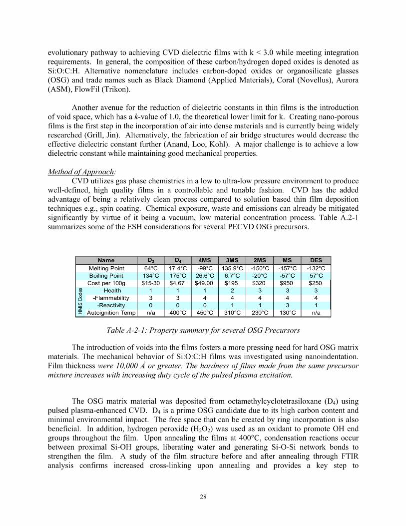
CVD utilizes gas phase chemistries in a low to ultra-low pressure environment to produce well-defined, high quality films in a controllable and tunable fashion. CVD has the added advantage of being a relatively clean process compared to solution based thin film deposition techniques e.g., spin coating. Chemical exposure, waste and emissions can already be mitigated significantly by virtue of it being a vacuum, low material concentration process. Table A.2-1 summarizes some of the ESH considerations for several PECVD OSG precursors.
D3 D4 4MS 3MS 2MS MS DES64°C 17.4°C -99°C 135.9°C -150°C -157°C -132°C
134°C 175°C 26.6°C 6.7°C -20°C -57°C 57°C$15-30 $4.67 $49.00 $195 $320 $950 $250
-Health 1 1 1 2 3 3 3-Flammability 3 3 4 4 4 4 4
-Reactivity 0 0 0 1 1 3 1Autoignition Temp n/a 400°C 450°C 310°C 230°C 130°C n/aH
MIS
Cod
es
NameMelting PointBoiling Point
Cost per 100g
Table A-2-1: Property summary for several OSG Precursors
The introduction of voids into the films fosters a more pressing need for hard OSG matrix materials. The mechanical behavior of Si:O:C:H films was investigated using nanoindentation. Film thickness were 10,000 Å or greater. The hardness of films made from the same precursor mixture increases with increasing duty cycle of the pulsed plasma excitation.
The OSG matrix material was deposited from octamethylcyclotetrasiloxane (D4) using pulsed plasma-enhanced CVD. D4 is a prime OSG candidate due to its high carbon content and minimal environmental impact. The free space that can be created by ring incorporation is also beneficial. In addition, hydrogen peroxide (H2O2) was used as an oxidant to promote OH end groups throughout the film. Upon annealing the films at 400°C, condensation reactions occur between proximal Si-OH groups, liberating water and generating Si-O-Si network bonds to strengthen the film. A study of the film structure before and after annealing through FTIR analysis confirms increased cross-linking upon annealing and provides a key step to

29
understanding the link between film structure and mechanical properties. For a deposition with a precursor flow rate ratio of H2O2 to D4 of 25:1 and an equivalent power of 30W, the T/D ration increased from 4.5 to 5 and a two fold increase in hardness (0.201 to 0.417 GPa) was observed upon annealing. In annealed diethylsilane (DES) films, the dielectric constant increases steadily from 2.64 to 2.91 as the flow rate of H2O2 increased from 5 to 25 sccm.
0
1
2
3
0 5 10 15 20 25 30
Flowrate of H2O2 (sccm)
Hard
ness
& M
odul
us (G
Pa)
Hardness, As DepositedHardness, AnnealedModulus, As DepositedModulus, Annealed
Figure A-2-5: Hardness and Modulus of Pulsed PECVD grown from D4/H2O2 mixtures
Nano-porous films were created by co-depositing the pulsed PECVD OSG matrix material with an organic porogen. Then, through an annealing or post-plasma treatment, the porogen is decomposed and removed from the film, leaving behind the porous matrix. Simultaneously polymerizing multiple precursors to create both the OSG and porogen phase can be challenging as their deposition conditions must overlap. To avoid this obstacle, polystyrene beads can be used as the porogen, thereby decoupling the process windows for the OSG and porogen phases. Another advantage to using beads is that the pore size and pore size distribution of the film is controlled. In addition, no covalent bonds between the matrix and porogen materials will be formed which eliminates disruptions in the matrix material after the porogen is removed.
Polystyrene is a prime candidate for the porogen due to its low degradation temperature
(below 400°C) and short decomposition time. A multilayer porous structure was constructed by a two step process of spraying and drying bead solution onto a wafer and then depositing the CVD OSG matrix material, which penetrates between the packed beads. Annealing removed the bead phase. The circular cross-section of the pores in Figure A-2-6 indicates that the matrix material was sufficiently rigid and did not collapse after porogen removal. Non-collapsing matrix structures are readily deposited from a diethylsilane/oxygen mixture by pulsed PECVD.

30
8 nm
(b)8 nm8 nm
(b)
Figure A-2-6 : Proof of concept for pores created in a CVD Si:O:C:H film using polystyrene beads as the porogen. The current goal is to create smaller, more randomly distributed pore
(courtesy of Qingguo Wu)
In initial studies, the beads used had a 96 nm mean diameter and thus could be easily seen by scanning electron microscopy (SEM). Using beads with 15 nm mean diameter give films with pores are too small to be easily seen by SEM. Thus, cross-sectional transmission electron micrograph (TEM), as shown in Figure A-2-6, is required. The circular cross-section of the pores in Figure A-2-6 indicates that the matrix material was sufficiently rigid and did not collapse after porogen removal. Non-collapsing matrix structures are readily deposited from a diethylsilane/oxygen mixture by pulsed PECVD
The polystyrene beads are available from Interfacial Dynamics Corporation with diameters ranging from 15 nm to 10 microns. The percent standard deviation of the diameter ranges from 4 to 6%. The beads are produced by emulsion polymerization and are dispersed in distilled de-ionized water. Polysciences Inc. also produces polystyrene beads as well as poly-methyl methacrylate beads, with sizes ranging from around 50nm to 125 microns. Polystyrene beads offer minimal environmental impact, since no additional precursor gases are needed. Styrene in air also has minor environmental, health and safety impacts, with a HMIS code of 1,0,1 for health, flammability and reactivity.
Reducing this process into one step would be preferable from a manufacturing
standpoint. The current reactor lid was redesigned to accommodate an ultrasonic atomizer. The ultrasonic atomizer will spray the bead solution into the vacuum chamber where the water will immediately vaporize leaving the polystyrene beads to deposit. This will facilitate simultaneous deposition and allow for random dispersal of beads throughout the film with a controllable degree of porosity. The limiting factor with polystyrene beads as the porogen is currently the smallest available is around 15 nm. An alternative porogen is cyclodextrin (CD), which is crystalline, water soluble, cyclic, non-reducing oligosaccharide. Three naturally occurring CDs are alpha cyclodextrin, beta cyclodextrin, and gamma cyclodextrin, of which beta cyclodextrin is mostly common used. Cyclodextrin is an ideal porogen candidate due to its low decomposition temperature and smaller molecular size, around 15.4Å in diameter. Investigations will be made into the environmental impacts of CD and its decomposition products.
31
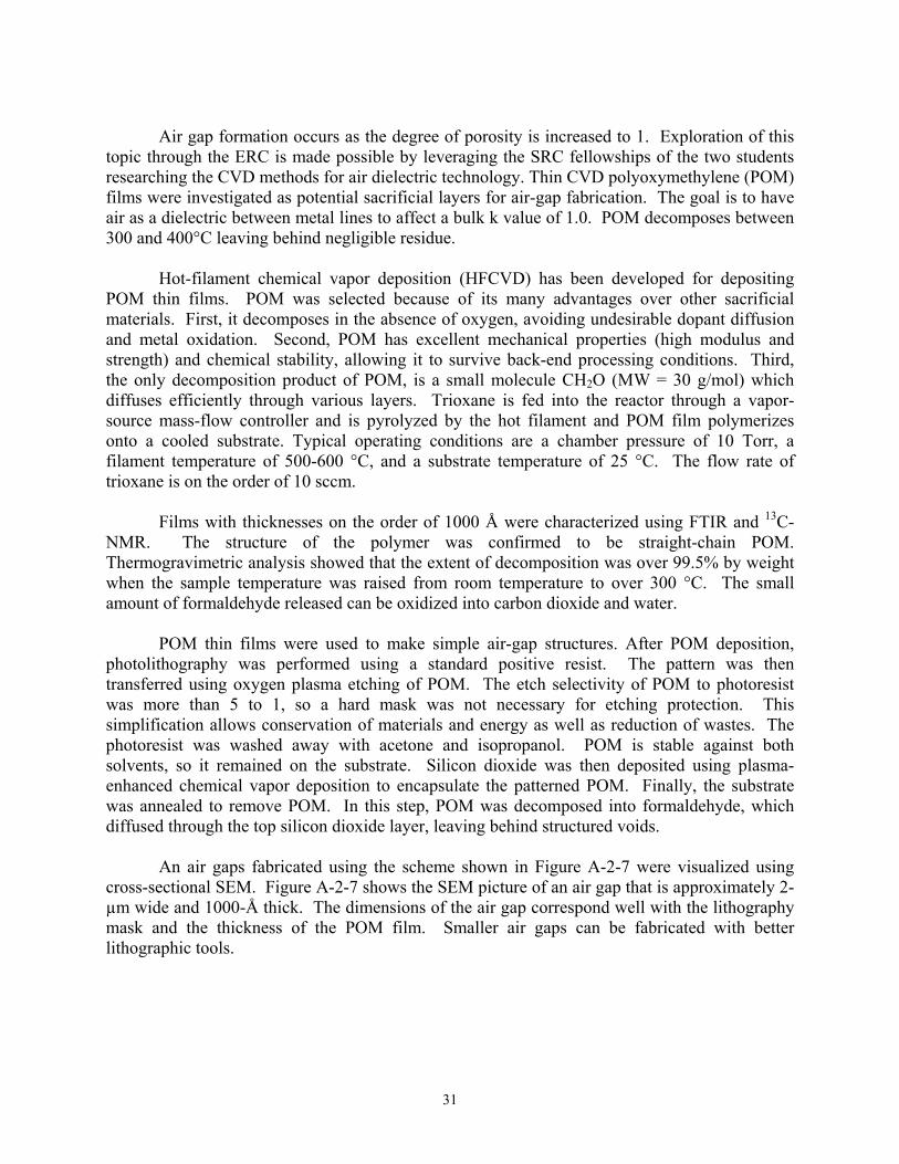
Air gap formation occurs as the degree of porosity is increased to 1. Exploration of this
topic through the ERC is made possible by leveraging the SRC fellowships of the two students researching the CVD methods for air dielectric technology. Thin CVD polyoxymethylene (POM) films were investigated as potential sacrificial layers for air-gap fabrication. The goal is to have air as a dielectric between metal lines to affect a bulk k value of 1.0. POM decomposes between 300 and 400°C leaving behind negligible residue.
Hot-filament chemical vapor deposition (HFCVD) has been developed for depositing
POM thin films. POM was selected because of its many advantages over other sacrificial materials. First, it decomposes in the absence of oxygen, avoiding undesirable dopant diffusion and metal oxidation. Second, POM has excellent mechanical properties (high modulus and strength) and chemical stability, allowing it to survive back-end processing conditions. Third, the only decomposition product of POM, is a small molecule CH2O (MW = 30 g/mol) which diffuses efficiently through various layers. Trioxane is fed into the reactor through a vapor-source mass-flow controller and is pyrolyzed by the hot filament and POM film polymerizes onto a cooled substrate. Typical operating conditions are a chamber pressure of 10 Torr, a filament temperature of 500-600 °C, and a substrate temperature of 25 °C. The flow rate of trioxane is on the order of 10 sccm.
Films with thicknesses on the order of 1000 Å were characterized using FTIR and 13C-
NMR. The structure of the polymer was confirmed to be straight-chain POM. Thermogravimetric analysis showed that the extent of decomposition was over 99.5% by weight when the sample temperature was raised from room temperature to over 300 °C. The small amount of formaldehyde released can be oxidized into carbon dioxide and water.
POM thin films were used to make simple air-gap structures. After POM deposition, photolithography was performed using a standard positive resist. The pattern was then transferred using oxygen plasma etching of POM. The etch selectivity of POM to photoresist was more than 5 to 1, so a hard mask was not necessary for etching protection. This simplification allows conservation of materials and energy as well as reduction of wastes. The photoresist was washed away with acetone and isopropanol. POM is stable against both solvents, so it remained on the substrate. Silicon dioxide was then deposited using plasma-enhanced chemical vapor deposition to encapsulate the patterned POM. Finally, the substrate was annealed to remove POM. In this step, POM was decomposed into formaldehyde, which diffused through the top silicon dioxide layer, leaving behind structured voids.
An air gaps fabricated using the scheme shown in Figure A-2-7 were visualized using
cross-sectional SEM. Figure A-2-7 shows the SEM picture of an air gap that is approximately 2-µm wide and 1000-Å thick. The dimensions of the air gap correspond well with the lithography mask and the thickness of the POM film. Smaller air gaps can be fabricated with better lithographic tools.

32
Figure A-2-7: Cross-Sectional Scanning Electron Microscopy Picture Depicting a 2-µm wide, 1000-Å tall Air Gap
Highlights of Results and Accomplishments:
• Rapid deposition of organosilicon films (>2.5 �m/min), providing efficient usage of materials and energy.
• Pulsed plasma enhanced chemical vapor deposition demonstrated to linearly tune the composition and mechanical properties of organosilicon low dielectric constant films.
• Film mechanical properties can be enhanced by reaction between proximal end groups that lead to a higher cross-linking.
• Demonstrated creation of spherical voids into CVD films using nanoscale polystyrene beads as the porogens.
• Modified reactor in utilize an ultrasonic atomizer to in vacuum bead deposition. • Polyoxymethylene deposited and shown as viable sacrificial materials for air gap
formation • Single-level air gap created
Interactions with Other ERC Projects:
Collaborating with Task A-1 to determine the characteristics and ESH impacts of the plasma etching processes for OSG films.
Task A-3: Plasma Tool Effluent Studies Personnel: PI:
• David Graves, Chemical Engineering, University of California at Berkeley
Graduate Students: • Cheng-Che Hsu, Chemical Engineering, UC-Berkeley • Mark Nierode, Chemical Engineering, UC-Berkeley
Undergraduate Students:
• David Flaherty, Chemical Engineering, UC-Berkeley • Michael Kasper, Chemical Engineering, UC-Berkeley • Chad Su, Chemical Engineering, UC-Berkeley (graduated May 03)

33
Other Researchers:
• Mikhail Sorokin, the Group of Elementary Processes in Gas Discharges, Eindhoven University of Technology
Objectives:
The nature of plasma tool effluents is poorly understood and is generally uncontrolled. A particularly important problem is the emission of global warming gases such as perfluorocarbons (PFCs). These gases are used for etching dielectric films, for CVD chamber cleaning, and for etch tool chamber cleaning. In some cases, PFCs pass through the plasma chamber without reacting, but in other cases, PFCs are created in the plasma. This project focuses on developing models of PFCs and etch products created in the plasma chamber from etch gas decomposition and from the etching process.
Background: Perfluorocompounds are widely used in semiconductor industry for dielectric films
etching and plasma-enhanced chemical vapor deposition (PECVD) and plasma etch chamber cleaning. Among various perfluorocompounds, C4F8 is frequently chosen because of its relatively high dissociation ratio, relatively low F/C ratio and acceptable price. However, effluent from plasmas using C4F8 often contains significant quantities of global-warming gases such as CF4 and C2F6. The focus of the present study is to develop experimental and modeling methods to predict emissions and ultimately to systematically reduce emissions.
The overall goal for this study is to develop models of plasma with C4F8, focusing
especially on CF4, C2F6 and related compound formation mechanisms. A well-diagnosed inductively coupled plasma-etching chamber was utilized in this study. An O2/C4F8 recipe for SiCN film etching was chosen for investigating the relation between the etching rate, deposition rate, and effluent species concentration. An Ar/C4F8 recipe with discharge only (without etching dielectric film) was chosen for the etch gas decomposition mechanism study. This report will highlight recent work regarding SiCN etching behavior in a O2/C4F8 plasma; Ar/C4F8 plasma composition analysis; and various CF4 formation mechanisms and overall C/F material balance in the plasma.
Method of Approach: Apparatus: inductively-coupled plasma etch system
A well-diagnosed plasma etch apparatus (see Figure A-3-1) was utilized in this project. The apparatus is inductively coupled plasma with inductive source power delivered to a top coil. A second source of RF power, substrate bias power, is delivered to the chuck holding the wafer with the film to be etched. Plasma density and ion energy impacting the substrate can be adjusted through alterations in source and bias power, respectively. Plasma species including etching by-products are detected using dual quadrupole mass spectrometers: one for ions and one for neutrals, both stable and radical species. A quartz crystal microbalance (QCM) immersed in the plasma measures rates of deposition of etch by-products or etch rates of selected films, such as electrode or dielectric films, chamber wall material, hard mask or photoresist material. Optical emission spectroscopy, Langmuir probe, and an ion flux probe are also used to characterize the plasma. A Fourier Transform Infrared (FTIR) absorption instrument is used to detect stable etch products in the chamber foreline. Measurements of plasma neutral and ionic species, as well as

34
effluent and wall deposit composition measurements allow an assessment of potential ESH impacts of the combination of new materials and etch gas combinations. Combining the inlet gases and materials with measurements of species in the plasma and effluent species will form the basis of a semi-empirical model of effluent composition based on materials, etch gases and operating conditions.
Figure A-3-1: Experimental plasma etching apparatus, showing both top and side views.
Major diagnostic instruments include mass spectrometers, optical emission spectrometry, and microbalance for re-deposited flux measurements.
Apparatus for Cross-section Measurement A project was initiated in the fall of 2003 with two undergraduate students and a retired senior visiting scholar (Harold Winters) to measure total dissociation cross sections for selected gases. This experiment is still being built, and has involved the participation of Air Products through gas donations. Highlights of Results and Accomplishments:
Low k Dielectric Film (SiCN) Etching: We report measurements of effluent species composition at downstream FTIR, as well as etch by-product, etching rate, and wall deposition rate on QCM from etching of SiCN films (Si 21%, C 21%, N 17%, and H 42%) with C4F8/O2 plasmas. In Figure A-3-2, the etching rate increased significantly as bias voltage increased while the deposition rate on the wall (QCM) remained constant. The downstream FTIR in Figure A-3-3 showed that significant amounts of SiF4, CF4, and C2F6 were measured in the tool effluent.

35
These trends show that it is the inlet gas decomposition chemistry, rather than the etching by-products, that dominate the effluent species composition and the wall deposition rate.
Figure A-3-2: SiCN film etching rate and wall deposition rate as a function of bias voltage under
following condition: C4F8 / O2: 10 / 2sccm, power 150W, and pressure 5mT.
Figure A-3-3: During SiCN film etching by C4F8 / O2, effluent species concentration under different bias voltage under following condition: C4F8 / O2: 10 / 2sccm, power 150W, and
pressure 5mT
-20 0 20 40 60 80 100 120 140
0
500
1000
1500
2000
2500
(<10A/min)Etch
ing/
Dep
ositi
ng R
ate
(Α/m
in)
Bias Voltage (V)
Etching Rate (SiCN film) Deposition Rate (on Microbalance)
0 10 20 30-2000
0
2000
4000
6000
40000
50000
60000
CF4 SiF4 C2F6
Time (minute)
FTIR
Sig
nal I
nten
sity
-20
0
20
40
60
80
100
120
140
160
BiasV Source
Source P
ower (W
)B
ias Voltage (V
)

36
In following studies, the industrially typical gas mixture of predominately Ar with C4F8 was chosen and used. Conditions were: Ar flow: 18 sccm, C4F8 flow: 2sccm; source power: 150W; gas pressure: 10mT.
Neutral Species Composition for Ar/C4F8 Discharge: The major neutral species in this discharge are shown in Figure A-3-4. In addition to Ar, the dominant species were F and CF2 and the densities were 2.43*1013 cm-3 and 1.38*1013 cm-3, respectively, and CF4 density was 0.76*1013 cm-3.
Figure A-3-4: Dominant neutral species density measured by using mass spectrometer under Ar: 18 sccm, C4F8: 2sccm, source power: 150W, and pressure: 10mT. Note that Ar density was
multiplied by 0.1.
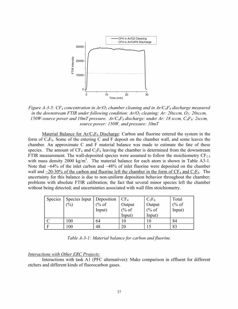
CF4 Formation Mechanism: According to this study, CF4 can be formed from: 1) Ar/C4F8 plasma, and 2) Ar/O2 chamber dry cleaning to clean the fluorocarbon wall film species. According to Figure A-3-4, ~2.5% of neutral species in the plasma was CF4, illustrating the first CF4 formation mechanism. This source of CF4 contributed at least 60% of the CF4 measured at the downstream FTIR. As shown in Figure A-3-5, during Ar/O2 plasma chamber cleaning under Ar (20sccm Ar and O2; 150W-source power and 10mT pressure), not only COF2 and CO, but also a significant amount of CF4 was measured in the downstream FTIR during cleaning.
Ar (
*0.1
)
C4F
8
CF4
CF3
CF2CFF
0
0.51
1.5
2
2.5
3 Density (10
13 cm-3)
37
Figure A-3-5: CF4 concentration in Ar/O2 chamber cleaning and in Ar/C4F8 discharge measured in the downstream FTIR under following condition: Ar/O2 cleaning: Ar: 20sccm, O2: 20sccm, 150W-source power and 10mT pressure. Ar/C4F8 discharge: under Ar: 18 sccm, C4F8: 2sccm,
source power: 150W, and pressure: 10mT
Material Balance for Ar/C4F8 Discharge: Carbon and fluorine entered the system in the form of C4F8. Some of the entering C and F deposit on the chamber wall, and some leaves the chamber. An approximate C and F material balance was made to estimate the fate of these species. The amount of CF4 and C2F6 leaving the chamber is determined from the downstream FTIR measurement. The wall-deposited species were assumed to follow the stoichiometry CF1.5 with mass density 2000 kg/m3. The material balance for each atom is shown in Table A3-1. Note that ~64% of the inlet carbon and ~48% of inlet fluorine were deposited on the chamber wall and ~20-30% of the carbon and fluorine left the chamber in the form of CF4 and C2F6. The uncertainty for this balance is due to non-uniform deposition behavior throughout the chamber; problems with absolute FTIR calibration; the fact that several minor species left the chamber without being detected; and uncertainties associated with wall film stoichiometry.
Species Species Input
(%) Deposition (% of Input)
CF4 Output (% of Input)
C2F6 Output (% of Input)
Total (% of Input)
C 100 64 10 10 84 F 100 48 20 15 83
Table A-3-1: Material balance for carbon and fluorine.
Interactions with Other ERC Projects:
Interactions with task A1 (PFC alternatives): Make comparison in effluent for different etchers and different kinds of fluorocarbon gases.
0 10 20 30
0
10000
20000
30000
FTIR
Inte
nsity
Time (min)
CF4 in Ar/O2 Cleaning CF4 in Ar/C4F8 Discharge

38
Task A-4: Waste Minimization Subtask A-4-1: Modeling of Pattern Dependency Effects Personnel: PI:
• Duane Boning, Electrical Engineering and Computer Science, MIT
Graduate Students: • Hong Cai, Material Science and Engineering, MIT • Xiaolin Xie, Physics, MIT
Other Researchers: • Tae Park, Electrical Engineering and Computer Science, MIT (Post-Doc)
Objectives: The goal of this project is to develop process modeling methods to minimize slurry, pad,
and water consumption in CMP processes through the modeling of pattern dependent effects.
Background: Chemical-mechanical polishing is a critical process for the most advanced interconnect
and device technologies, as it enables dielectric planarization, shallow trench isolation, plug formation, and copper damascene processes. The process is a major consumer of resources (slurry, water), and producer of waste and effluents (pads, spent slurry).
The process is poorly understood and controlled, which exacerbates the waste problem, including frequent use of monitor and look-ahead wafers. Much of the difficulty associated with CMP results from pattern dependency: the lines or structures patterned on a wafer polish differently, depending on the feature size and the structures nearby. In addition, each different product (with a different chip layout) also polishes differently, requiring substantial fine-tuning of the process to address “thin” and “thick” locations across the chip.
Method of Approach: Models of CMP, particularly models of planarization of patterned topographies, will be
developed, and optimization methods created which use these models to minimize process time, deposition thicknesses, slurry use, and waste production. We are taking a semi-empirical approach, pictured in Figure A-4-1-1, in which characterization test structures and test masks are designed and used to gather experimental data. In previous work, we developed a set of test masks for oxide CMP (for use with aluminum interconnect technology) that consist of arrays of different line and space combinations resulting in different layout pattern densities. Previous work demonstrated that for oxide CMP, pattern density is the dominant factor. For STI CMP, we are investigating new test structures and patterns that are more appropriate for the feature types used in transistor and isolation areas. In the case of copper CMP, we are making extensive use of MIT designed test masks, particularly the Sematech 854 test mask, which provides a large number of line and space as well as pattern density combinations for experimental characterization of the dishing and erosion that result as a function of multiple layout parameters.
In all of these applications, a model which accounts for pattern density and pattern step height effects is fit to the experimental data. The models can then be used to predict dishing and erosion in arbitrary new product layouts. At present, models can account for the effect of polish time, but are not parameterized in terms of other process parameters (such as relative velocity,

39
pressure, or slurry parameters). Rather, the process dependence is capture empirically and the effect of that characterized process on different patterns and layouts is predicted.
Figure A-4-1-1 – Overview of CMP pattern dependent modeling methodology.
Highlights of Results and Accomplishments:
Over this year, this subtask has focused on pattern dependent issues in the shallow trench isolation (STI) CMP process (copper CMP modeling is discussed in subtask A6-2). Key results include (1) a re-examination of the physical basis for the planarization length concept which has been the central idea in the MIT CMP models; (2) development of a relationship for the “contact height” as a function of layout parameters, which is needed to improve our pattern-density/step-height based model; (3) development of a new STI CMP test mask with length, width, and space dimensions as variables to more closely resemble realistic STI structures, and (4) exploration of the potential impact of wafer nano-topography on STI dishing and erosion.
The first pair of accomplishments has resulted from the use of an alternative CMP modeling approach – contact wear simulation – to better understand the basis for, and improve, the simplified pattern-density/step-height model developed at MIT. Briefly, the MIT model makes use of two approximations. The first is that the CMP removal rate is inversely proportional to an effective pattern density, i.e. those regions with high raised area pattern density (approaching 100%) polish slowly (approaching the blanket removal rate), while those with low percentage of raised material polish more rapidly. A fundamental component of this model is the calculation of “effective pattern density” which is a weighted average (e.g. using a Gaussian or other filter function) of the layout pattern density. The “planarization length” determines the width or size of this filter function: a longer planarization length (e.g. 8-10 mm)

40
means that the CMP pad and process average the chip pattern quite effectively, which a shorter planarization length (e.g. 3 mm) means that substantial local polish non-uniformities within the chip are likely. The second key approximation in the MIT model is that zero down area polish (in the low region between two neighboring lines or features) occurs when the step height is above some “contact height.” Once the up areas have been polished to within this distance of the down area, then the polish pressure is apportioned between both up and down areas resulting in a decrease in planarization efficiency.
To understand the approximations and improve the MIT model, an alternative modeling approach has also been implemented. Contact wear simulations explicitly treat the polish pad as an elastic medium, and calculate (on a discretized basis) the deflection of the pad into low areas and the localized pressure of the pad on up and down areas. A key parameter in this model is the effective elastic modulus of the polishing pad. As an example, Figure A-4-1-2 shows a profile evolution based on contact wear simulation; these simulations are computationally intensive and thus are not possible across the entire chip. However, contact wear simulations shed light on both the planarization length approximation and the step height or contact height approach in the MIT model. As shown in Figure A-4-1-3, the up and down area removal rates as functions of step height show that the MIT approximation is reasonable. A new exponential (as opposed to piecewise linear) removal rate relationship for the MIT model is being developed to improve this approximation. Also in Figure A-4-1-3, a functional dependence of the contact height is fit to layout parameters based on the contact wear simulations. Finally, a linear relationship between the planarization length and effective pad modulus has also been found.
Figure A-4-1-2 – Profile evolution over a 60 second polish at 5 second intervals, using a contact wear simulation approach.

41
Figure A-4-1-3: Left; Comparison between step-height and contact wear model relationships between pressure and feature step height.
Right; Extracted fit of contact height to line width and pattern density parameters, based on contact wear simulations.
The second key accomplishment in this subtask has been to apply a combination of the contact wear and pattern-density/step-height model to understand the implications of nano-topography on STI CMP. In previous experimental work, it has been shown that wafer nano-topography, or 10-50 nm height variations on virgin wafers occurring over lateral distances of several millimeters, can result in excess thinning of surface oxide layers during CMP. No experimental results are yet available with patterned wafers and nano-topography, so we explored the possible impact using a modeling approach.
We used actual nano-topography surface height wafer maps measured by ADE Corp., and then simulated what dishing and erosion would occur on a patterned wafer with and without this nano-topography. As seen in Figure A-4-1-4, the nitride erosion with and without nano-topography varies appreciably. Further experimental and simulation work is needed to better understand how important nano-topography may be in future IC technology generations.
Step-height model
Contact-wear model

42
Figure A-4-1-4 – Simulated nitride erosion when all overburden oxide is removed. (a) Without nano-topography. (b) With nano-topography. Color scale in Å.
Interactions with Other ERC Projects: Coupling with other CMP projects in Task A is underway. In particular, the use of the
STI CMP model with the motor current sensor work by Philipossian is being developed, and will enable improved layout-dependent endpoint detection.
Next-Year Plans:
• Analyze experimental data from a new STI CMP test mask, gathered in collaboration with National Semiconductor, and extend CMP model as necessary to account for rectangular as opposed to long line features
• Develop a model relating wafer surface pattern evolution to motor current-based endpoint detection signals, in order to optimize detection for different wafer layouts
Long-Term Plans:
• Develop and transfer a methodology and model for chip-scale prediction and optimization of dishing and erosion performance in advanced CMP processes.
Subtask A-4-2: Fluid Dynamics Analysis and Tribological Characterization Personnel: PI:
• Ara Philipossian, Chemical and Environmental Engineering, UA
Other Researchers: • Yun Zhuang, Chemical and Environmental Engineering, UA • Partick Levy (visiting researcher at UA from Pall Corporation) • Yoshitomo Shimazu (visiting researcher at UA from Showa Denko)

43
Graduate Students: • Zhonglin Li, Chemical and Environmental Engineering, UA • Yasa Samporno, Chemical and Environmental Engineering, UA
Undergraduate Students:
• Deanna King, Chemical and Environmental Engineering, UA • Kelly Brink, Chemical and Environmental Engineering, UA
Objectives:
The main objectives of this subtask are to (1) reduce the use of blanket copper wafers by replacing them with copper discs during preliminary screening of new slurries and pads for frictional and tribological attributes, (2) reduce slurry dispense volumes for copper polish through fundamental understanding of the thermal and kinetic attributes of copper CMP, (3) establish analytical and functional baselines for fresh and spent slurries for ILD CMP applications and develop method to reprocess spent slurry utilizing filtration and separation techniques, and (4) understand the: extent and mechanism of contact and wear between the wafer, the cerium oxide abrasives and the pad during ILD and STI CMP applications and determine the effect of key processing conditions on silicon dioxide and silicon nitride removal rate. Each objective is addressed below.
Method of Approach, Highlights of Results and Accomplishments:
Collectively, these studies adopt a series of experimental techniques ranging from real-time coefficient of friction (COF) and temperature analysis to thermal modeling of the pad and wafer temperature during oxide and copper CMP. Experiments are performed using a scaled version of a Speedfam-IPEC 472 polisher. The polisher is placed on a, and synchronized to, a friction table so that the real-time friction data can be obtained. An infrared camera is used to record the pad surface temperature at a frequency of 5 Hz at ten points along the outer periphery of the wafer.
In the case of copper discs or wafers, a precise balance (readability 0.01 mg) and an
automatic four-point probe are used to measure the weight and thickness before and after polishing to calculate removal rate. All copper discs, have a nominal diameter of 100 mm and a purity of 99.99 percent. As for 100-mm copper deposited wafers, they are comprised of three layers as follows: 20,000 Angstroms of PVD copper, followed by 1,000 Angstroms of PVD Ta, followed by 1,000 Angstroms of thermal silicon dioxide grown on p-type silicon substrate. In the case of oxide wafers, they are all 100-mm silicon wafers with10,000 Angstroms of thermally grown silicon dioxide.
To determine the dominant tribological mechanism during CMP, Stribeck curves are
presented using a dimensionless grouping of CMP-specific parameters, called the Sommerfeld number:
δ
µpUSo = (1)

44
In the above equation µ is the slurry viscosity, U is the relative pad-wafer average linear velocity, p is the applied wafer pressure, and δ is the effective slurry thickness in the pad-wafer region. Determination of U and µ are fairly straightforward as the latter can be measured experimentally for a given slurry, while the former depends on tool geometry and angular velocities of wafer and the platen. Wafer pressure is defined as the applied down force divided by the apparent contact area between the wafer and the pad. Depending on its groove design, each pad will experience a different pressure when subjected to the same down-force. To account for this, a dimensionless parameter, α, which represents the area of the up-features divided by the area to a flat pad, is used to scale the wafer pressure. Subsequently, applied pressure is divided by α (0.83 for the case of IC-1000 K-groove pad) to determine the actual pressure experienced by the wafer. The final parameter necessary for the calculating the Sommerfeld number is the effective slurry film thickness, which was measured using the following expression:
( ) grooveaR δααδ ×−+×= )1( (2) Pad roughness (Ra) values were taken using a stylus profiler. The relative standard derivation for surface roughness was less than 10 percent for all the values measured. The final parameter necessary for calculation of δ is the groove or perforation depth (i.e. δgroove) of each pad, which was physically, measured using calipers. Coefficient of friction (COF) is defined as the ratio of shear to normal force:
normal
shear
FF
COF = (3)
The plot of COF vs. the Sommerfeld number is known as the Stribeck curve and gives direct evidence of the extent of wafer-slurry-pad contact. When plotting COF as a function of the Sommerfeld number three major modes of contact can be envisaged. The first mode of contact is ‘boundary lubrication’ where all solid bodies are in intimate contact with one another and COF does not depend on Sommerfeld number. The second mode is ‘partial lubrication’ where the wafer and the pad are partially contacting each other. As the Stribeck curve transitions from ‘boundary lubrication’ to ‘partial lubrication’, the slope of the line measuring COF becomes negative. Finally, the ‘hydrodynamic lubrication’ mode of contact occurs at larger values of the Sommerfeld number where the fluid film layer totally separates the pad and the wafer, and COF once again becomes independent of Sommerfeld number albeit at a much lower value. For a given Stribeck curve, average COF represents the arithmetic average of all COF values taken at various Sommerfeld numbers.
For a given polishing run, the measured total unidirectional shear force as a function of time can be broken up into two components (a mean force component and a fluctuating force component) as shown in Eq. 4 below:
)()( tfFtFshear += (4)
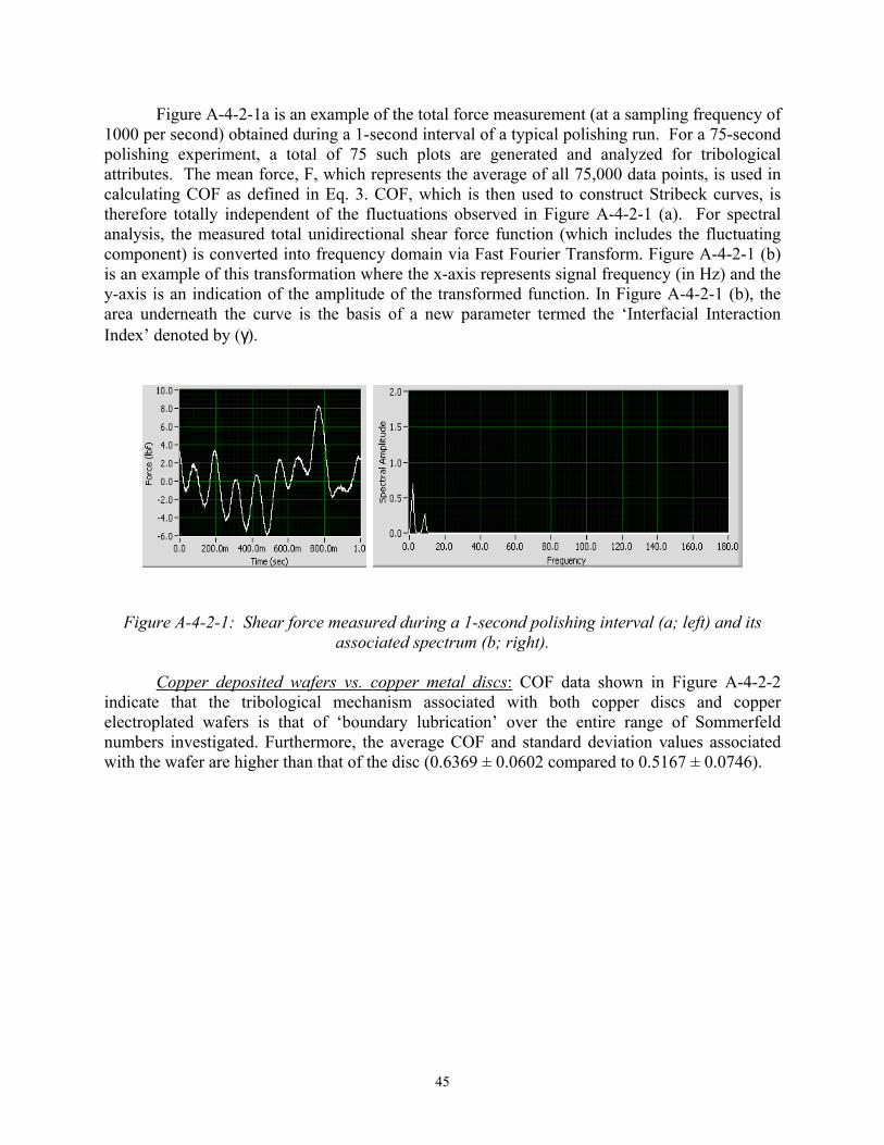
45
Figure A-4-2-1a is an example of the total force measurement (at a sampling frequency of 1000 per second) obtained during a 1-second interval of a typical polishing run. For a 75-second polishing experiment, a total of 75 such plots are generated and analyzed for tribological attributes. The mean force, F, which represents the average of all 75,000 data points, is used in calculating COF as defined in Eq. 3. COF, which is then used to construct Stribeck curves, is therefore totally independent of the fluctuations observed in Figure A-4-2-1 (a). For spectral analysis, the measured total unidirectional shear force function (which includes the fluctuating component) is converted into frequency domain via Fast Fourier Transform. Figure A-4-2-1 (b) is an example of this transformation where the x-axis represents signal frequency (in Hz) and the y-axis is an indication of the amplitude of the transformed function. In Figure A-4-2-1 (b), the area underneath the curve is the basis of a new parameter termed the ‘Interfacial Interaction Index’ denoted by (γ).
Figure A-4-2-1: Shear force measured during a 1-second polishing interval (a; left) and its associated spectrum (b; right).
Copper deposited wafers vs. copper metal discs: COF data shown in Figure A-4-2-2
indicate that the tribological mechanism associated with both copper discs and copper electroplated wafers is that of ‘boundary lubrication’ over the entire range of Sommerfeld numbers investigated. Furthermore, the average COF and standard deviation values associated with the wafer are higher than that of the disc (0.6369 ± 0.0602 compared to 0.5167 ± 0.0746).

46
0.1
1.0
1.0E-04 1.0E-03 1.0E-02Sommerfeld Number
CO
FCu discCu wafer
Figure A-4-2-2: Stribeck curve for copper disc and copper wafer
This difference may be explained as follows: • There are differences in the shape of the wafer bevel (relatively sharp edge) compared
to the disc (rounded-off edge). This difference stems from the fact that the edge of the wafer retains its shape during polishing since the thickness of the copper deposited layer (20 microns) is only 0.4 percent of the total thickness of the wafer (~ 500 micron). In stark contrast, during CMP, the copper metal disc is polished along its flat surface as well as its edge, thus its bevel become progressively rounder as polishing proceeds.
• Copper wafer is thicker than the copper disc by about 20 percent (i.e. 500 vs. 400 micron)
Rounded-off edge … Since sides are polished as well as the surface
Disc
Rounded-off edge … Since sides are polished as well as the surface
DiscSharp edge … Since the silicon bulk prevents the wafer bevel to be polished by copper slurry
Wafer
Sharp edge … Since the silicon bulk prevents the wafer bevel to be polished by copper slurry
WaferWafer
Figure A-4-2-3: A schematic of the contact and ‘ploughing’ model between the pad and copper disc (left) and copper wafer (right)
As the substrate comes into contact with the pad, the thicker wafer with its sharper edge
is more likely to ‘plough’ into the pad at its leading edge thus resulting in higher values of COF. In fact, the penetration depth of a wafer into IC-1000 pad is around 20 microns, which supports this ’ploughing’ effect. This qualitative model is shown in Figure A-4-2-3. Investigating the frictional waveforms and their associated spectra further strengthens the above hypothesis. Figure A-4-2-4 shows the corresponding spectra. At 2.5 PSI and 1.09 m/s, a
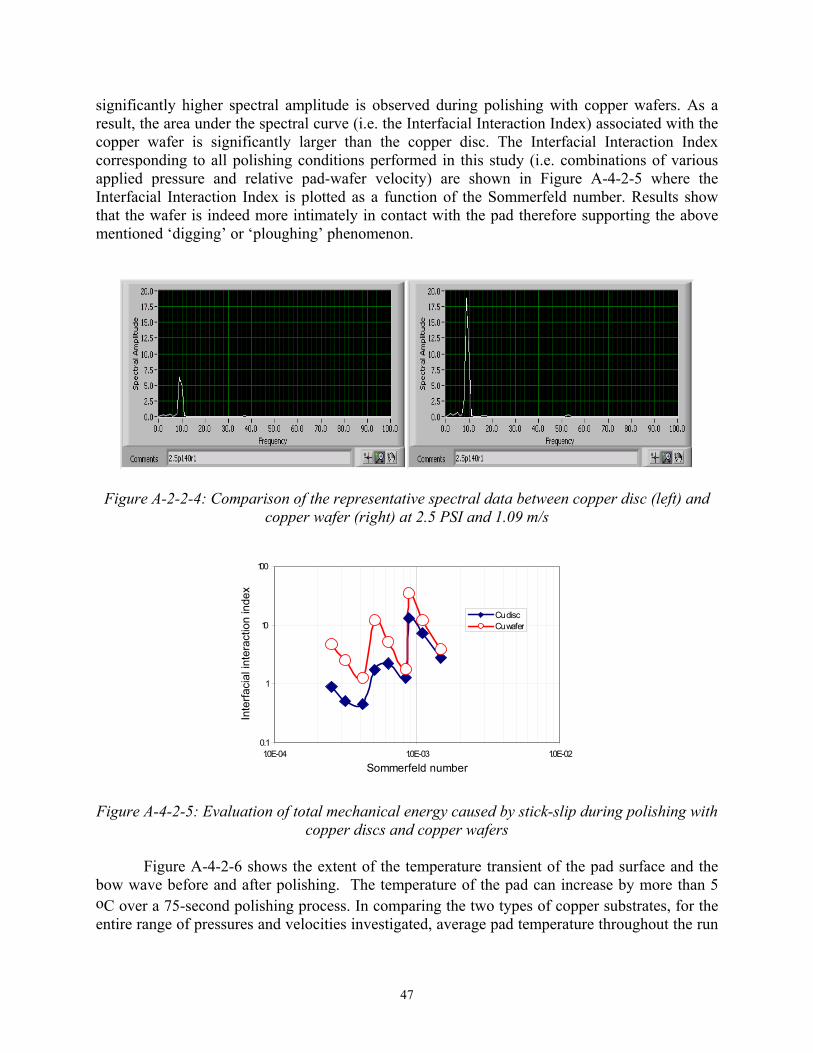
47
significantly higher spectral amplitude is observed during polishing with copper wafers. As a result, the area under the spectral curve (i.e. the Interfacial Interaction Index) associated with the copper wafer is significantly larger than the copper disc. The Interfacial Interaction Index corresponding to all polishing conditions performed in this study (i.e. combinations of various applied pressure and relative pad-wafer velocity) are shown in Figure A-4-2-5 where the Interfacial Interaction Index is plotted as a function of the Sommerfeld number. Results show that the wafer is indeed more intimately in contact with the pad therefore supporting the above mentioned ‘digging’ or ‘ploughing’ phenomenon.
Figure A-2-2-4: Comparison of the representative spectral data between copper disc (left) and copper wafer (right) at 2.5 PSI and 1.09 m/s
0.1
1
10
100
1.0E-04 1.0E-03 1.0E-02
Sommerfeld number
Inte
rfaci
al in
tera
ctio
n in
dex
Cu discCu wafer
Figure A-4-2-5: Evaluation of total mechanical energy caused by stick-slip during polishing with
copper discs and copper wafers
Figure A-4-2-6 shows the extent of the temperature transient of the pad surface and the bow wave before and after polishing. The temperature of the pad can increase by more than 5 oC over a 75-second polishing process. In comparing the two types of copper substrates, for the entire range of pressures and velocities investigated, average pad temperature throughout the run

48
is 1 degree Celsius higher for the copper wafer. This is consistent with the COF results noted above since higher values of COF indicate greater energy dissipation in the form of heat.
With respect to removal rate, Figure A-4-2-7 indicates that material removal is slightly higher for the copper wafer compared to copper disc. This is consistent with a thermally activated copper removal rate model. Given the fact COF is directly proportional to temperature (due to frictional energy dissipation in the form of heat), the removal rate findings are consistent with both frictional and thermal results. It is noteworthy that the extrapolated dynamic etch rates (which represent the true chemical removal rate in the absence of any mechanical effects) associated with both discs and wafers are very close to one another (see the y-intercept of the individual curves in Figure A-4-2-7). This is not surprising since dynamic etch rate is mostly governed by the type of slurry used (i.e. PL-7102).
0
1
2
3
4
5
6
7
0 5000 10000 15000 20000
Pressure x Velocity (Pa-m/s)
Pad
Tem
p. T
rans
ient
(deg
C) Cu disc
Cu wafer
Figure A-4-2-6: Pad temperature transients as a function of various pressure and pad-wafer
velocity combinations
FigureA-4-2-7: Removal rate as a function of pressure and pad-wafer velocity
0
2000
4000
6000
8000
10000
0 2000 4000 6000 8000 10000 12000 14000 16000 18000 20000
Pressure x Velocity (Pa-m/s)
Rem
oval
Rat
e (A
/min
)
Cu disc
Cu wafer

49
Copper slurry flow rate studies: Figure A-4-2-8 shows the Stribeck curves associated with the two flow rates. Over the range of Sommerfeld numbers considered, the Stribeck curves are close to being constant, which implies that the tribological (wear) mechanism is the same in all cases. The mean COF at 80 cc/min is 0.517 while at 140 cc/min it is only slightly lower at 0.491. COFs of this magnitude are consistent with boundary lubrication in which pad asperities make direct contact with the wafer.
FigureA-4-2-8: Stribeck curves for various slurry flow rates
FigureA-4-2-9: Removal rate as a function of pressure and pad-wafer velocity for various slurry flow rates
0.1
1.0
1.0E-04 1.0E-03 1.0E-02
Sommerfeld Number
CO
F
80 cc/min
140 cc/min
0
2000
4000
6000
8000
0 5000 10000 15000 20000
Pressure x Velocity (Pa-m/s)
Rem
oval
Rat
e (A
/min
)
80 cc/min
140 cc/min
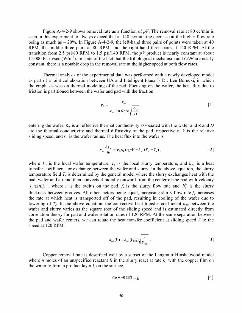
50
Figure A-4-2-9 shows removal rate as a function of pV. The removal rate at 80 cc/min is seen in this experiment to always exceed that at 140 cc/min, the decrease at the higher flow rate being as much as ~ 20%. In Figure A-4-2-9, the left-hand three pairs of points were taken at 40 RPM, the middle three pairs at 80 RPM, and the right-hand three pairs at 140 RPM. At the transition from 2.5 psi/80 RPM to 1.5 psi/140 RPM, the pV product is nearly constant at about 11,000 Pa-m/sec (W/m2). In spite of the fact that the tribological mechanism and COF are nearly constant, there is a notable drop in the removal rate at the higher speed at both flow rates.
Thermal analysis of the experimental data was performed with a newly developed model as part of a joint collaboration between UA and Intelligent Planar’s Dr. Len Borucki, in which the emphasis was on thermal modeling of the pad. Focusing on the wafer, the heat flux due to friction is partitioned between the wafer and pad with the fraction
DVrw
w
w
κκ
κγ627.0
2
+= [1]
entering the wafer. κw is an effective thermal conductivity associated with the wafer and κ and D are the thermal conductivity and thermal diffusivity of the pad, respectively, V is the relative sliding speed, and rw is the wafer radius. The heat flux into the wafer is
)()(2 swwskw
w TThpVtz
T−−=
∂∂ µγκ , [2]
where Tw is the local wafer temperature, Ts is the local slurry temperature, and hws is a heat transfer coefficient for exchange between the wafer and slurry. In the above equation, the slurry temperature field Ts is determined by the general model where the slurry exchanges heat with the pad, wafer and air and then convects it radially outward from the center of the pad with velocity
)2/( 0rhf ss π , where r is the radius on the pad, fs is the slurry flow rate and 0sh is the slurry
thickness between grooves. All other factors being equal, increasing slurry flow rate fs increases the rate at which heat is transported off of the pad, resulting in cooling of the wafer due to lowering of Ts. In the above equation, the convective heat transfer coefficient hws between the wafer and slurry varies as the square root of the sliding speed and is estimated directly from correlation theory for pad and wafer rotation rates of 120 RPM. At the same separation between the pad and wafer centers, we can relate the heat transfer coefficient at sliding speed V to the speed at 120 RPM,
120120)()(
VVVhVh wsws = . [3]
Copper removal rate is described well by a subset of the Langmuir-Hinshelwood model
where n moles of an unspecified reactant R in the slurry react at rate k1 with the copper film on the wafer to form a product layer L on the surface,
LnRCu k→+ 1 [4]
51
The reacted layer is then removed by mechanical abrasion with rate k2,
LL k→ 2 . [5] The abraded material L is carried away by the slurry and is not re-deposited. The local removal rate in this sequential mechanism is
2
1
1
1kCk
CkMRR w
+=
ρ, [6]
where Mw is the molecular weight of copper, ρ is the density, and C is the local molar concentration of reactant. It is assumed that there is little reactant depletion so that C remains constant. This allows C to be absorbed into k1. In the above equation, the rate of the chemical reaction is expressed as )/exp(1 wkTEAk −= with C = 1. Assuming that the mechanical removal rate is proportional to pV, then pVck p=2 where cp is an assumed proportionality constant. In the mechanically-limited extreme, the polish rate is ( )pVcMRR pw ρ/= and in the opposite limit it is
( ) 1/ kMRR w ρ= .
The model was then calibrated and run for all pressures, rotation rates and flow rates. The measured COF from each condition was smoothed with a linear regression line. The ambient temperature that was employed as an initial condition in each case for the pad, wafer and slurry and for calculating convective heat loss to the air was estimated by averaging the initial temperatures measured on the pad. The model then provided the wafer temperature field needed for computing reaction rates. Next, starting with the estimated mean wafer temperatures for each condition, the parameters A, E and cp were calculated by minimizing the least squares error between the predictions and the measured rates. The optimum values, A = 2.7x10⁸ moles/m2-sec, E = 0.68 eV, and cp = 2.2x10⁻⁷ moles/Pa-m3 provided a root mean square fitting error of 313 Angstroms. Using the model, the underlying causes for changes in removal rate at the 2.5 PSI/80 RPM-to-1.5 PSI/140 RPM transition (at which pV is nearly constant) were investigated. At a constant flow rate of 140 cc/min, the ambient temperature, COF function, heat partition fraction and wafer-slurry heat transfer coefficient were systematically switched from the 1.5 PSI/140 RPM condition to the 2.5 PSI/80 RPM condition. It was found that the ambient temperature, COF and heat partition fraction accounted for about 40% of the temperature change with the latter two accounting for most of the difference and having about equal influences. About 55% of the difference was due to a change in the convective cooling coefficient, and the remainder is accounted for by the fact that pV is not precisely constant across the transition. Figure A-4-2-10 shows how the model (solid line) compares with the experimental data (discrete points) at a slurry flow rate of 140 cc/min. Overall, this work indicates that changing the slurry flow rate (in order to provide a more environmentally benign process) must be carefully considered due to its effects on process temperature and therefore thermally activated removal rate ramifications.

52
Figure A-4-2-10: Comparison of model and experimental data for the case of 140 cc/min slurry flow rate
ILD slurry filtration and regeneration: The goals of this undertaking were to characterize regenerated fumed silica slurry used in ILD CMP utilizing filtration techniques, and to determine if they could be rendered analytically and functionally equivalent to fresh slurries. The results presented in Figure A-4-2-11 show that multiple polishes had little effect on viscosity (2.41 compared with 2.39 cp), and specific gravity (1.081 compared with 1.077). The change in specific gravity corresponded to only a 0.15 percent drop in solids content (from 12.50 to 12.35 percent). Results in Figure A-4-2-12 show that slurry recycling had little effect on pH (11.00 compared with 10.85) but a notable effect on metal levels as highlighted by a 3-fold increase (3 compared to 1ppm).
The results presented in Figure A-4-2-13 show that multiple polishes also had notable effects on both mean aggregate size, and large particle count (LPCs). There was an 11 percent increase in mean aggregate size (138 compared to 150 nm) after reusing the slurry 5 times. Also, there was a 50-fold increase in LPCs (>1.0 microns) for the unfiltered material when comparing fresh slurry with 5 times recycled slurry. In the case of filtered slurry there was only a 3X increase in LPCs when comparing fresh filtered with 5 times recycled filtered slurry. Moreover, all of the filtered slurry samples had notably lower LPCs than the initial fresh unfiltered slurry (at least 3X). Slurry filtration did not have a major impact on the above metrics except possibly on mean aggregate size (although it appears that multiple reuses of the slurry had a greater impact), and on LPCs. In that case, filtration was quite effective in reducing the number of LPCs (especially in the case of the recycled slurries where the reduction was greater than 2 orders of magnitude).
0
2000
4000
6000
8000
0 5000 10000 15000 20000
Pressure x Velocity (Pa-m/s)
Rem
oval
Rat
e (A
/min
)
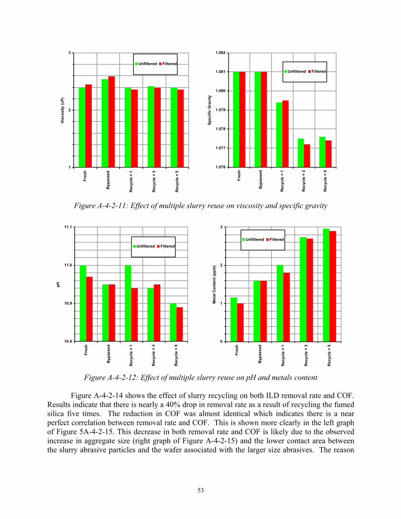
53
Figure A-4-2-11: Effect of multiple slurry reuse on viscosity and specific gravity
Figure A-4-2-12: Effect of multiple slurry reuse on pH and metals content Figure A-4-2-14 shows the effect of slurry recycling on both ILD removal rate and COF.
Results indicate that there is nearly a 40% drop in removal rate as a result of recycling the fumed silica five times. The reduction in COF was almost identical which indicates there is a near perfect correlation between removal rate and COF. This is shown more clearly in the left graph of Figure 5A-4-2-15. This decrease in both removal rate and COF is likely due to the observed increase in aggregate size (right graph of Figure A-4-2-15) and the lower contact area between the slurry abrasive particles and the wafer associated with the larger size abrasives. The reason
1
2
3
Fres
h
Byp
asse
d
Rec
ycle
= 1
Rec
ycle
= 3
Rec
ycle
= 5
Visc
osity
(cP)
Unfiltered Filtered
1.076
1.077
1.078
1.079
1.080
1.081
1.082
Fres
h
Byp
asse
d
Rec
ycle
= 1
Rec
ycle
= 3
Rec
ycle
= 5
Spec
ific
Gra
vity
Unfiltered Filtered
10.8
10.9
11.0
11.1
Fres
h
Byp
asse
d
Rec
ycle
= 1
Rec
ycle
= 3
Rec
ycle
= 5
pH
Unfiltered Filtered
0
1
2
3
Fres
h
Byp
asse
d
Rec
ycle
= 1
Rec
ycle
= 3
Rec
ycle
= 5
Met
al C
onte
nt (p
pm)
Unfiltered Filtered
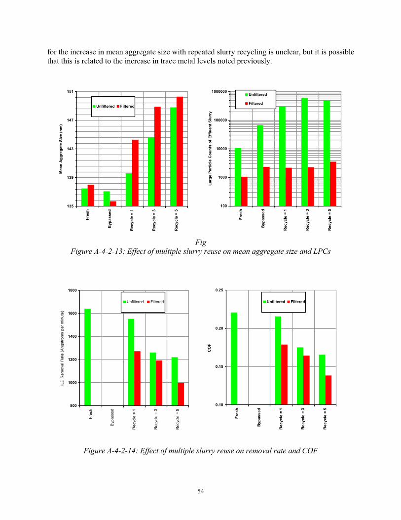
54
for the increase in mean aggregate size with repeated slurry recycling is unclear, but it is possible that this is related to the increase in trace metal levels noted previously.
Fig Figure A-4-2-13: Effect of multiple slurry reuse on mean aggregate size and LPCs
Figure A-4-2-14: Effect of multiple slurry reuse on removal rate and COF
135
139
143
147
151Fr
esh
Byp
asse
d
Rec
ycle
= 1
Rec
ycle
= 3
Rec
ycle
= 5
Mea
n A
ggre
gate
Siz
e (n
m)
Unfiltered Filtered
100
1000
10000
100000
1000000
Fres
h
Byp
asse
d
Rec
ycle
= 1
Rec
ycle
= 3
Rec
ycle
= 5
Larg
e Pa
rtic
le C
ount
s of
Effl
uent
Slu
rry
Unfiltered
Filtered
800
1000
1200
1400
1600
1800
Fres
h
Bypa
ssed
Rec
ycle
= 1
Rec
ycle
= 3
Rec
ycle
= 5
ILD
Rem
oval
Rat
e (A
ngst
rom
s pe
r min
ute)
Unfiltered Filtered
0.10
0.15
0.20
0.25
Fres
h
Byp
asse
d
Rec
ycle
= 1
Rec
ycle
= 3
Rec
ycle
= 5
CO
F
Unfiltered Filtered

55
Figure A-4-2-15: Correlations among COF, removal rate and mean aggregate size ILD and STI CMP with cerium oxide slurries: In CMP abrasives in the slurry play vital
roles in the kinetic and frictional attributes of the process. In recent years, slurries containing cerium oxide abrasives have become increasingly popular in ILD and STI applications. Use of these slurries results in a dramatic reduction in the amount of the solids content. Abrasive content may be as high as 30 percent by weight for conventional colloidal silica slurries and as high as 12.5 percent by weight for fumed silica slurries at the point of use. On the other hand, in cerium oxide slurries, solids content is typically less than 1 percent by weight. This reduction is beneficial due to cost as well as solids waste discharge points of view. Moreover, for STI applications, cerium oxide slurries have demonstrated superior oxide-to-nitride removal rate selectivity essential for successful process integration. While there have been a multitude of studies focusing on the combined kinetic and tribological attributes of ILD CMP using silica-based slurries, little information is known regarding possible correlations between removal rate and coefficient of friction in CMP processes employing cerium oxide slurries. Study of the combined kinetic and frictional attributes of a process is essential due to at least two counteracting phenomena. On one hand, coefficient of friction has been shown to directly relate to ILD removal rate, and thus, in the absence of other phenomena, improved throughput. On the other hand, it has been shown that the extent of frictional forces and the lubrication mechanism by which the CMP proceeds can impact pad life. Increased frequency of pad changes can adversely affect tool availability (and throughput) due to the fact that pad change, pad break-in and pad re-qualification can take away hours of otherwise useful production time from a polishing tool. This study aims to understand the effect of cerium oxide slurry type, cerium oxide abrasive concentration and relative pad-wafer velocity affect the frictional, tribological and kinetic attributes of the process.
Figure A-4-2-16 shows Stribeck curves corresponding to ILD and nitride polishing using
cerium oxide slurries with three different solids concentrations. In all cases, an IC-1000 k-groove pad is used. COF values corresponding to ceria-based slurries are significantly higher than those of silica based-slurries (the latter are typically around 0.25). For ILD polish, solids content has a dramatic effect on COF such that higher values of COF are attained at lower solids concentrations. This is not the case for nitride polishing. Also, for ILD polish proceeds via ‘boundary lubrication’ for 1 and 0.5 percent solids and ‘partial lubrication’ for 0.25 percent solids. In the case of nitride polishing, regardless of solids content, lubrication mechanism seems to be that of ‘partial lubrication’.
900
1100
1300
1500
1700
0.13 0.15 0.17 0.19 0.21 0.23
COF
ILD
RR
(A/m
in)
900
1100
1300
1500
1700
135.0 140.0 145.0 150.0 155.0
Mean Aggregate Size (nm)
ILD R
R (A
/min)

56
Figure A-4-2-17 shows the corresponding removal rate plots. Removal rate actually increases with decreasing solids content hinting at the possibility that, similar to silica-based slurries, COF and removal rate may be directly related. An interesting correlation is seen between the lubrication regime and the extent of Prestonian behavior such that ‘boundary lubrication’ results in Prestonian behavior. When polishing takes place in ‘partial lubrication’ or in the transition region between the two lubrication regimes, removal rate tends to proceed in a non-Prestonian fashion.
Figure A-4-2-16: Stribeck curves corresponding to ILD (left) and nitride (right) CMP processes
Figure A-4-2-17: Removal rate plots corresponding to Figure A-4-2-16 Previous studies at UA have shown a linear relationship between removal rate and COF
for silica-based slurries regardless of the type of pad and silica solids content (as long as the solids content was higher than 6 percent by weight). Figure A-4-2-18 indicates that this trend continues to hold for cerium oxide based slurries explored in this study. Ceria slurries are found to operate at higher values of COF, thus providing more points over a larger range of values.

57
Figure A-4-2-18: Correlation between COF and removal rate for cerium oxide based slurries (diamond, triangle and square symbols) and its relationship to silica-based slurries (circles)
Interactions with Other ERC Projects:
Real-time thermography of the CMP process is through collaboration with MIT’s Duane Boning. The main goal of this project is to correlate COF, lubrication mechanism, process temperature and removal rate to each other for both copper and ILD processes on small-scale as well as industrial-scale polishers.
Next-Year Plans:
• Determine whether the ‘universal’ relationship between removal rate and COF applies to copper polishing as well as ILDF polishing with colloidal silica slurries
• Explore the utility of the ‘interfacial interaction index’ on copper and ILD polish applications
• Develop second generation thermal model to aide in improved kinetics analysis of ILD and copper processes and extend the model to industrial-scale polishers
• Fully explore (both experimentally and through simulation) the effect of slurry flow rate on copper polish
Long-Term Plans:
• Develop fundamental models relating process tribology to pad life. • Develop fundamental models relating removal rate, COF, lubrication mechanism,
particle morphology and process temperature to one another. • Develop prototype for ILD slurry filtration and regeneration
Task A-5: Fundamental Pad Characterization and Modeling Personnel: PI:
• Ara Philipossian, Chemical and Environmental Engineering, UA • Toshiroh Doi, Chemical and Environmental Engineering, UA
0.00E+00
5.00E-14
1.00E-13
1.50E-13
2.00E-13
2.50E-13
3.00E-13
3.50E-13
4.00E-13
0.00 0.20 0.40 0.60 0.80 1.00 1.20
Average COF
Pre
ston
's C
onst
ant (
1/P
a)
XY-groove Perforated
Flat
K-groove
0.25 %
0.25 %1.00 %
0.50 %0.50 0.50
1.00 %
1.00 %0.25 %
Source: Silica-based slurry … Philipossian & Olsen (MRS 2003)
58
• Duane Boning, Electrical Engineering and Computer Science, MIT
Other Researchers: • Yun Zhuang, Chemical and Environmental Engineering, UA (Post-Doc) • Len Borucki (part-time visiting researcher at UA from Intelligent Planar)
Graduate Students:
• Jam Sorooshian, Chemical and Environmental Engineering, UA • Daniel Rosales-Yeomans, Chemical and Environmental Engineering, UA • Leslie Charns, Chemical and Environmental Engineering, UA • Xiaolin Xie, Electrical Engineering and Computer Science, MIT
Undergraduate Students:
• Masano Sugiyama, Chemical and Environmental Engineering, UA Objectives:
The main objectives of this task are to (1) develop and evaluate new pad groove designs to improve the frictional, flow and removal rate characteristics of ILD CMP, (2) determine the impact of pattern density on the effective pressure (a.k.a. envelope pressure) during STI CMP, and (3) determine the mechanical attributes of a new class of non-porous CMP pads containing water soluble particles (WSP). Attaining the above goals will allow pad manufacturers to identify and control critical pad parameters for reduced variability, longer pad life and improved planarization performance.
Method of Approach, Highlights of Results and Accomplishments:
Collectively, these studies adopt a series of experimental techniques ranging from real-time coefficient of friction (COF) and temperature analysis to thermal modeling of the pad and wafer temperature during oxide and copper CMP. Experiments are performed using a scaled version of a Speedfam-IPEC 472 polisher (described previously under Subtask A-4-2) as well as an industrial Speedfam-IPEC Avanti 472 polisher (150-mm wafers) located at Sandia National Laboratories.
Novel pad grooving design studies: As shown in Figure A-5-1, the groove designs included Flat, Lemniscate, Logarithmic Spiral Positive and Logarithmic Spiral Negative. Patterns were formed by a programmable milling machine. In order to attain the logarithmic spiral designs, grooves were first formed spirally on the pad starting from the center so as to facilitate stable slurry supply in the pad-wafer region. Next, in order to improve slurry utilization and increase removal rates, logarithmic grooves were formed along the radius of the spirally grooved pad. The precise shape of the logarithmic grooves was determined following detailed flow visualization studies by tracing polishing debris ejected from the pad surface during CMP. As a result, such grooves were expected to facilitate the discharge of unwanted by-products.
Figure A-5-2 summarizes the effect of Sommerfeld number on COF for the various groove designs. The Logarithmic Spiral Negative pads show the highest average COF followed by Logarithmic Spiral Positive pads, Flat pads and Lemniscate pads. The shapes of the individual Stribeck curves indicate that both types of Logarithmic Spiral pads remain in ‘boundary

59
lubrication’ throughout the range of parameters studied. The Lemniscate pad begins in ‘boundary lubrication’ and shows a tendency to migrate to ‘partial lubrication’ as Sommerfeld numbers increase. The tribological mechanism of the Flat pad seems to be similar to the Lemniscate, pad but to a lesser extent. For purposes of clarity, error bars, which were no more than ± 5 and ± 10 percent for COF and Sommerfeld number, respectively, are not shown in the figures below. Trends are explained further in the following section.
Figure A-5-1: Groove designs used in this study; Lemniscate pad (top left); Flat (top right); Logarithmic Spiral Positive (bottom left); Logarithmic Spiral Negative (bottom right).
0.10
1.00
1.00E-05 1.00E-04 1.00E-03 1.00E-02 1.00E-01
Sommerfeld Number
Ave
rage
Coe
ficie
nt o
f Fric
tion
Leminscate
Logarithmic-Spiral-Negative
Logarithmic-Spiral-Positive
Flat
Figure A-5-2: Stribeck curves corresponding to various groove designs.
For all types of pads studied, Figure A-5-3 shows that average removal rate (represented by Preston’s constant) and average COF are directly related. Values represent an average of at least 4 experiments with all values falling within ± 5 percent of one another. This trend is very consistent with previously reported linear relationship between average COF and removal rate

60
for various pads and slurry concentrations and suggests the presence of a ‘universal relationship’ between the two factors as previously seen in Subtask A-4-2.
The significant difference in the COF between the Logarithmic Spiral Negative pad (i.e. 0.414) and the Logarithmic Spiral Positive pad (i.e. 0.284) is due to the fact that the former pad, with its logarithmic grooves formed in the direction opposite to the rotation of the platen, causes the slurry to discharge away from the wafer due to centrifugal forces. On the other hand, the Logarithmic Spiral Positive pad, with its grooves in same direction as that of the rotation of the platen, works to increase slurry flow around the wafer. The presence of excess slurry around the periphery of the wafer has been previously shown to significantly reduce COF in the wafer-pad region. This decrease, coupled with the near-linear relationship between COF and removal rate mentioned above, explains the 11 percent lower removal rate associated with the Logarithmic Spiral Positive pad. Figure A-5-3: Relationship between COF and Preston’s constant for various groove designs .
Figures A-5-4 and A-5-5 show the spectral attributes of the four pads at minimum (i.e. 6 PSI and 0.31 m/s) and maximum (i.e. 2 PSI and 0.93 m/s) values of Sommerfeld number, respectively. Regardless of the particular pressure, velocity or groove design, all spectra contain fundamental peaks at 1 and 9 Hz. The peak at 1 Hz is believed to be due to tool kinematics since angular velocities for the pad, the wafer and the diamond disk range from 30 to 120 RPM. This corresponds to frequencies ranging from 0.5 to 2 Hz. The reason for the presence of the peak at 9 Hz (with its harmonic peaks at 18 and 36 Hz) is currently unknown. However, since it is always present during processing, it may be related to the specific configuration of the polishing tool and its related ancillary hardware. Studies are currently underway to identify the potential root cause. The most interesting feature of the above spectra is the presence of a fundamental peak at about 90-95 Hz corresponding to the Lemniscate, Flat and Logarithmic Spiral Negative pads. This peak occurs to some extent regardless of the particular choice of pressure or velocity, however it is most pronounced at low Sommerfeld numbers (i.e. Figure 5). Such high frequencies correspond to events that recur every 11 milliseconds, which are believed to be due to the reduction of slurry in the wafer-pad interface, which in turn increases wafer-pad contact, thus enhancing stick-slip phenomena. The ‘non-presence’ of this peak in cases where a Logarithmic
1.0E-14
7.0E-14
1.3E-13
1.9E-13
2.5E-13
0.1 0.2 0.3 0.4 0.5Average Coeficient of Friction
Pres
ton'
s C
onst
ant (
1/Pa
)
Lemniscate
Logarithmic Spiral Negative Logarithmic Spiral Positive
Flat

61
Spiral Positive pad is used, is attributed to the directionality of the logarithmic grooves that promote slurry penetration in the wafer-pad region thus reducing hydrodynamic chattering. These results are in agreement with the average COF values reported in Figure 4 and help confirm the role of the logarithmic grooves in rejecting slurry from, or attracting slurry into, the wafer-pad region.
Figure A-5-4: Spectra corresponding to the Lemniscate pad (top left), Flat pad (top right), Logarithmic Spiral Positive pad (bottom left) and Logarithmic Spiral Negative pad (bottom
right) obtained at minimum Sommerfeld number.
Figure A-5-5: Spectra corresponding to the Lemniscate pad (top left), Flat pad (top right), Logarithmic Spiral Positive pad (bottom left) and Logarithmic Spiral Negative pad (bottom
right) obtained at maximum Sommerfeld number.

62
Envelope pressure and pattern density studies: Removal rate results obtained from the 150-mm polisher coupled with a proven removal rate model (based on a simplified Langmuir-Hinshelwood kinetics mechanism described in Subtask A-4-2) has allowed determination of effective pressure during CMP of Shallow Trench Isolation (STI) wafers. Polishing tests were performed at controlled platen temperatures of approximately 15, 23, 35 and 45°C. HDP-filled STI wafer pattern densities of 10, 50 and 90 percent were used. Wafers were polished with Cabot D7300 fumed-silica slurry at a solids weight percent of 12.5 percent. Rodel’s IC-1400 K-grooved pad was employed for all experiments. Tests were performed at a linear velocity of 0.5 m/s and applied wafer pressures of 3 and 7 PSI. Real-time IR thermography of the pad surface, at the leading and trailing edges of the wafer, indicated that thermal transients were not pattern dependent, but rather a function of velocity and pressure. The apparent activation energy for the STI polishing process was calculated to be approximately 0.2 eV for all pattern densities, pressures and velocities investigated. Based on the simplified Langmuir-Hinshelwood kinetics mechanism, the fact that process temperature was independent of pattern density indicated that any observed differences in material removal rate should be a result of pressure differences among wafers with various pattern densities. Based on this premise, effective pressure could be ‘back-calculated’ or derived from observed removal rate data and compared to applied pressure for a given polishing process. Results indicated that regardless of applied wafer pressure and platen temperature, the ratio of the derived effective pressure to applied wafer pressure was 2.2, 1.7 and 1.3 for 10, 50 and 90 percent density wafers respectively. The relative consistency of these ratios indicated that, in the extreme case of a nine-fold increase in pattern density (i.e. from 10 percent to 90 percent), the effective pressure experienced during polishing was not impacted by the pattern density in a proportionate manner. These findings are believed to have significant implications in all CMP processes where shear force needs to be controlled or minimized (i.e. for copper or low-k applications) for a wide range of pattern densities.
Characterization of pads with water soluble particles: CMP pads are critical to material removal of the device being polished. These amorphous cross-linked polymeric pads are often comprised of polyurethane with added fillers to enhance the hardness of the material. Surface asperities contribute to the mechanical abrasion while the pores and grooving contribute to slurry transport beneath the wafer. This study compares a conventional porous IC-1000 pad to non-porous pads comprised of a mixture of polymer and a Water Soluble Particle (WSP). Surface conditioning on the WSP pad provides enough agitation to cause the particles below the pad surface to dissolve. Cavities, formed as a result from the particle dissolution on the surface, act as pores to enhance asperity contact and to help transport slurry beneath the wafer.
CMP by nature is a thermally dependent process, thus characterizing material properties as a function of temperature is an appropriate method of describing the actual effects during polishing. During CMP the dynamic shear force present in the pad-slurry-wafer interface causes the temperature to rise significantly at the pad surface. This study emphasizes the correlation between observed temperature rises in the polishing pad to measured physical pad properties in the temperature region of 20 to 40 °C (i.e. standard ILD CMP operating temperatures). Performing dynamic (thermo-analytical) analysis of pads provides the mechanical properties while taking into account energy dissipation during deformation. Physical properties analyzed include glass transition temperature, Tg, storage modulus, E’, loss modulus, E”, tan δ, and Young’s modulus, E. Glass transition temperatures are characteristic of amorphous polymers and represent a narrow temperature region where a polymer in its solid state will change to a

63
‘rubbery’ state above that region. This change is not a phase change but rather a relaxation in the polymer chains. Properties such as hardness, brittleness and coefficient of thermal expansion undergo rapid changes around Tg. Storage modulus represents the modulus of the elastic portion of the material. Hence, it is a measure of the energy stored in the material and recovered per cycle. Conversely, the loss modulus is defined as the viscous portion of the material and measures the energy dissipated as heat due to deformation in the cycle (energy dissipated as heat, is never recovered). The ratio of the loss to the storage modulus is defined as tan δ and represents the material’s ability to dissipate energy. Such analyses are especially important in the case of unknown polymer formulations in order to observe viscoelastic response of the material.
Four types of polishing pads are compared in this study. The IC-1000 is used as a control experiment since there is much published data surrounding this type of pad. The other three are pads with varying amounts of WSP supplied by JSR Corporation. The content of WSP embedded into the pads has been normalized as follows:
a) ‘No WSP’ pad – no particles embedded in the pad b) ‘Standard WSP’ pad – standard content of particles embedded in the pad c) ‘High WSP pad’ – high content of particles embedded in the pad
The three pads vary only in their WSP content and do not differ in their polymer
composition. The pads are concentrically grooved and do not include a sub-pad. All pads were subjected to the same experimental conditions before DMA testing. Pads underwent a 30-minute initial condition and were tested with 5 dummy wafers before polishing experiments were conducted. The polishing parameters consisted of polishing 100-mm thermally grown silicon dioxide wafers at three relative pad-wafer velocities (0.31, 0.62 and 0.93 m/s) and three wafer pressures (2, 4 and 6 PSI). The set of polishing runs performed on each pad consisted of polishing under all combinations of pressure and velocity with one repetition. The slurry used for polishing was the JSR CMS1101 oxide slurry at a nominal pH of 10.5. All pads were conditioned ex-situ for one minute after each polishing run using a 325-grit diamond disc with a nominal down pressure of 1 PSI. In all cases, the oscillation frequency and the rotational speed of the disc was maintained at 0.33 Hz and 30 RPM, respectively. After polishing, the pads were rinsed and set to dry for DMA analysis.
Temperature data recorded by the IR camera show increasing transient regions for
increasing values of pressure and velocity (p × U) during polishing. The one-minute polish runs demonstrate that high (p × U) combinations result in transient regions of up to 25 seconds before a steady state temperature is achieved. Figure A-5-6 shows the difference in temperature increase at the surface of the pad for two different (p × U) combinations. The 2 PSI and 0.31 m/s combination only increase about 1 °C whereas the high combination yields an increase of 8.4 °C.
Table A-5-1 shows the temperature increase for a one-minute polish at the highest value of (p × U) (i.e. 6 PSI & 0.93 m/s) for each pad. The ‘No WSP’ pad exhibits the least amount of heating whereas the IC-1000 pad exhibits the greatest temperature increase at 9.4°C. Due to the rapid increase of temperature resulting from shear and normal forces exerted onto the pad by the wafer, mechanical property data was then employed to assess the polymer response in that temperature range. Glass transition temperature results recorded from the peak in the loss

64
modulus curve (Figure A-5-7) indicate that all WSP-containing pads have values of Tg ranging between 19.8 and 25.0 °C (Table 2).
Figure A-5-6: Real-time temperature results of the pad surface for a Standard WSP pad.
Top curve (2 PSI and 0.31 m/s); Bottom curve (6 PSI and 0.93 m/s)
Table A-5-1: Pad Temperature transients for a 1-minute polish at 6 PSI and 0.93 m/s
Figure A-5-7: Summary of loss modulus curves
The IC-1000 has a Tg at – 18 °C but its loss modulus peak is not as prominent as the peak on a WSP-containing pad. The WSP-containing pads also have a secondary relaxation between – 80 and – 63 °C as noted on Figure A-5-7. Relaxation transitions are denoted as α, β and γ in order of decreasing temperature. The α peak (relaxation at the highest temperature) represents
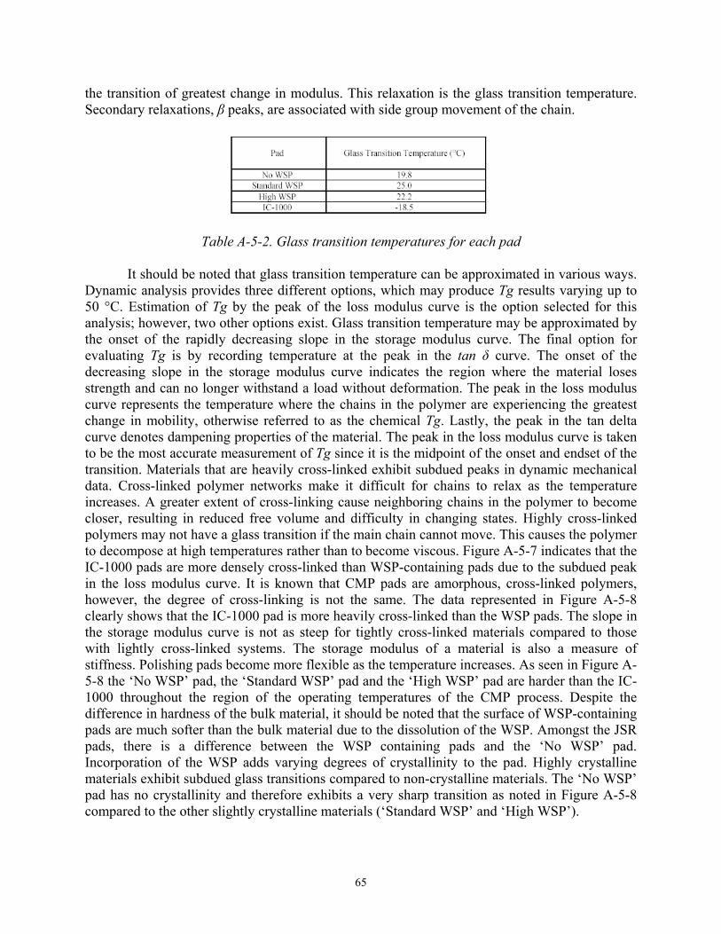
65
the transition of greatest change in modulus. This relaxation is the glass transition temperature. Secondary relaxations, β peaks, are associated with side group movement of the chain.
Table A-5-2. Glass transition temperatures for each pad
It should be noted that glass transition temperature can be approximated in various ways.
Dynamic analysis provides three different options, which may produce Tg results varying up to 50 °C. Estimation of Tg by the peak of the loss modulus curve is the option selected for this analysis; however, two other options exist. Glass transition temperature may be approximated by the onset of the rapidly decreasing slope in the storage modulus curve. The final option for evaluating Tg is by recording temperature at the peak in the tan δ curve. The onset of the decreasing slope in the storage modulus curve indicates the region where the material loses strength and can no longer withstand a load without deformation. The peak in the loss modulus curve represents the temperature where the chains in the polymer are experiencing the greatest change in mobility, otherwise referred to as the chemical Tg. Lastly, the peak in the tan delta curve denotes dampening properties of the material. The peak in the loss modulus curve is taken to be the most accurate measurement of Tg since it is the midpoint of the onset and endset of the transition. Materials that are heavily cross-linked exhibit subdued peaks in dynamic mechanical data. Cross-linked polymer networks make it difficult for chains to relax as the temperature increases. A greater extent of cross-linking cause neighboring chains in the polymer to become closer, resulting in reduced free volume and difficulty in changing states. Highly cross-linked polymers may not have a glass transition if the main chain cannot move. This causes the polymer to decompose at high temperatures rather than to become viscous. Figure A-5-7 indicates that the IC-1000 pads are more densely cross-linked than WSP-containing pads due to the subdued peak in the loss modulus curve. It is known that CMP pads are amorphous, cross-linked polymers, however, the degree of cross-linking is not the same. The data represented in Figure A-5-8 clearly shows that the IC-1000 pad is more heavily cross-linked than the WSP pads. The slope in the storage modulus curve is not as steep for tightly cross-linked materials compared to those with lightly cross-linked systems. The storage modulus of a material is also a measure of stiffness. Polishing pads become more flexible as the temperature increases. As seen in Figure A-5-8 the ‘No WSP’ pad, the ‘Standard WSP’ pad and the ‘High WSP’ pad are harder than the IC-1000 throughout the region of the operating temperatures of the CMP process. Despite the difference in hardness of the bulk material, it should be noted that the surface of WSP-containing pads are much softer than the bulk material due to the dissolution of the WSP. Amongst the JSR pads, there is a difference between the WSP containing pads and the ‘No WSP’ pad. Incorporation of the WSP adds varying degrees of crystallinity to the pad. Highly crystalline materials exhibit subdued glass transitions compared to non-crystalline materials. The ‘No WSP’ pad has no crystallinity and therefore exhibits a very sharp transition as noted in Figure A-5-8 compared to the other slightly crystalline materials (‘Standard WSP’ and ‘High WSP’).

66
Figure A-5-8: Summary of storage modulus data Another physical property that was measured was the elastic modulus. The slope of the
linear portion of the engineering stress stain curve determines Young’s modulus. Storage modulus results obtained from a DMA can be used as a comparison for the elastic modulus since the storage modulus is defined as the elastic portion of the material. In Table 3 the comparison of storage modulus to elastic modulus is made. In each case, the storage modulus is greater but the trend remains the same among the four pads. There is a greater difference between storage and elastic modulus for the JSR pads than the IC-1000 due to loss properties of the pads. It should be noted, however, that the loss difference cannot be quantified accurately since various frequency and load parameters may be changed on each method of analysis to result in a different response. This comparison is to show that for the given sample analysis parameters held constant, there are different responses for the different pads. Table 3 further demonstrates the loss difference between the pads with corresponding tan δ values for temperatures between 20 and 40 °C. The tan δ value for the IC-1000 is more than twice lower than the lowest value corresponding to WSP-containing pads. This correlates to the difference in moduli observed in Table 3.
Table A-5-3. Summary of storage modulus averaged between 20 and 40°C, and the elastic modulus.

67
Table A-5-4. Tan delta average values between 20 and 40 °C.
Next-Year Plans:
• Complete work on de-coupling of the chemical and mechanical attributes of CMP through controlled removal rate vs. temperature experiments (ILD and copper).
• Determine the effect of novel pad grooving on copper and ILD polish on 200-mm platform.
• Complete DMA and TMA characterization of various types of pads and determine the extent of their effect on COF, thermal transients and removal rate for ILD and copper CMP processes
Long-Term Plans:
• Propose and validate a pad design with improved ESH and process characteristics Task A-6: Alternative Planarization Technologies Subtask A-6-1: Copper CMP Using Fixed Abrasive Pads Personnel: PI:
• Srini Raghavan, Materials Science and Engineering, UA
Graduate Students: • Creighton Andersen, Materials Science and Engineering, UA • Kim Lueng, Materials Science and Engineering, UA • Subramanian Tamilmani, Materials Science and Engineering, UA
Undergraduates:
• Winston Benally, Dine College, Tsaile, AZ (Summer REU) Objectives:
The objective of this project is to understand the mechanisms underlying the removal of copper films using pads that contain embedded abrasive particles (FAP) with the ultimate goal of developing environmentally benign chemistries for copper CMP. In fixed abrasive pad CMP processes, the choice of a chemical system consisting of oxidant, complexant and corrosion inhibitor is very critical. The specific objectives are as follows: (1) to elucidate the effect of chemicals on removal rates and particle generation, (2) to characterize the extent of galvanic corrosion between copper and barrier metal during abrasion and (3) to find an inhibitor that is more environmentally benign than benzotriazole (BTA) and has comparable performance characteristics.

68
Background:
Fixed abrasive pads (FAP) differ from conventional pads in their morphology and consequently may be expected to remove material in a different manner. A fixed abrasive pad employs an array of polymer surface asperities embedded with small (~ 120nm) abrasive particles. The movement of asperities on FAP under load on the surface of films to be planarized can be likened to a fretting corrosion process. The removal of copper and the fate of removed copper depend on the chemistry employed in the CMP process. If a proper combination of chemistry and pH is not employed, the removed copper could form particulates during the planarization process.
Metals like tantalum, titanium and their nitrides are commonly used as barrier layers between copper and dielectric layers. During, as well as at the end of the barrier polishing step, copper and the barrier metal would be electrically connected, while being exposed to polishing solution. Due to differences in the electrochemical characteristics of copper and tantalum, the Cu-Ta couple is prone to galvanic corrosion. The galvanic corrosion between Cu and Ta has been discussed in the literature based on polarization curves 1 and it is generally agreed that Ta forms the anode in the galvanic cell. However, direct measurement of galvanic corrosion during polishing has not been reported in the literature. An understanding of the galvanic corrosion during polishing with FAP pads is likely to aid in the development of polishing chemistries to minimize barrier layer corrosion.
Benzotriazole (BTA) is a well-known corrosion inhibitor for copper in various applications in a wide range of environments. It is generally accepted that BTAH (as well as BTA - ion) chemisorbs on the copper surface and forms an insoluble cuprous surface complex. Though benzotriazole provides good protection, there are some environmental issues with the use of BTA. Hydroxamic acids, RCONHOH, chelate cupric ions very strongly and have long been considered for drug applications2. The effectiveness of hydroxamic acids to inhibit copper corrosion would depend on the nature of ‘R’ group. It is also important that hydroxamic acids are comparable to BTA in terms of rapid repassivation of freshly abraded copper surface.
Method of Approach:
Electrochemical studies on Cu and Ta were conducted in an electrochemical abrasion cell. The polishing pressure was fixed at 8.6 psi for all experiments. The fixed abrasive pad (0.7 cm2) was rotated at 240 rpm and the wafer sample was rotated at 222 rpm using two different computer controlled stepper motors. Electrochemical data were obtained using an EG&G PARC 263A potentiostat. A three-electrode setup was used for all electrochemical experiments. The reference electrode was a silver/silver chloride (Ag/AgCl) electrode with a luggin probe, and the counter electrode was platinum. The data from the electrochemical polarization experiments were used to determine the corrosion current density of the samples. The physical removal rates were calculated from surface profiles obtained using a KLATencor P2 profilometer. The samples were spin coated with photoresist prior to experiments to prevent static etching of the unabraded area of the samples during abrasion. The area of samples that was subjected to polishing was approximately 2 ± 0.5 cm2.
Galvanic corrosion experiments were carried out on the same abrasion apparatus using a
specially designed sample holder. Copper and tantalum samples (3 cm × 1.5 cm) were placed

69
side by side with a thin (< 0.5 mm) insulating silicone layer between their edges. The sample (Cu/Ta) was placed on a stack of two copper foils separated by an insulating material. A thin aluminum foil was used to make electrical contact between the Ta portion of the sample and one of the circular copper foils. The Cu part of the sample was connected to the other copper foil at the bottom through the window in the copper foil on top. Connections to the potentiostat were achieved via carbon brushes pressing against the rotating copper foils. Tantalum was made as the working electrode in all these experiments.
Etching and electrochemical experiments (no abrasion) with various inhibitors were
conducted in the abrasion/polishing cell at a sample rotation of 240 rpm. A three-electrode setup was used to make electrochemical measurements. Atomic absorption spectroscopy was used to determine the amount of copper removed from each sample. Turbidity readings were also collected to determine the amount of suspended particles in each waste stream. Highlights of Results and Accomplishments:
The removal rates (measured by a profiler) of copper in 3.6% (1.2 M) hydrogen peroxide solutions are shown in Figure A-6-1-1 (a) as a function of pH. The removal rate in hydrogen peroxide solutions slightly increases with increasing pH in the range 3 to 5 but falls off at higher pH values. The peroxide based chemistry, as may be evident from the turbidity of solutions, results in the generation of particulates. Roughly, a turbidity of ~35 NTU corresponds to 0.03 wt % of 70 nm colloidal silica particles. In the pH range of 3 to 7, the turbidity shows a peak in the vicinity of pH 5.5. The turbidity begins to rise again at pH values above 7. The trend of copper removal rate with respect to pH is the same as that of the amount of particulate generated with respect to pH. When more copper was removed, more particulates were generated.
Removal rates of copper in 1.2M hydrogen peroxide containing 0.01M citric acid were studied as function of pH and the results are shown in Figure A-6-1-1 (b). It may be noted that the removal rates in the presence of citric acid are almost five times greater than under conditions without citric acid. In contrast to the results obtained with peroxide only solutions, at acidic pH values the removal rates are high and the solution turbidity levels are low in the presence of citric acid. In a weak alkaline condition, at pH ~8, both the removal rates of copper and the turbidity are low. The presence of citric acid greatly reduces the turbidity of the solution.
The removal rates of copper using FAP in 0.5M hydroxylamine-based solutions are shown in Figure A-6-1-1 (c) as a function of pH. The figure shows a maximum in copper removal rates (~ 800 Å/min) at pH 6. The removal rates fall rapidly in the acidic and alkaline conditions away from pH 6. The amount of particulates generated (shown as turbidity) was very small in the entire pH range.
The variation of copper removal rates and solution turbidity with pH values in peroxide only solutions can be explained as follows. In acidic conditions, copper can be removed as cupric ions and this is the reason that the solution turbidity remains low. At pH values higher than 5.5, any dissolved copper in peroxide chemistry is likely to form CuO and contribute to the turbidity of the solution. It is also possible to form CuO directly from copper through a cuprous oxide intermediate at pH values slightly greater than 6. Abrasion of the oxide layer would also contribute to the turbidity of the solution. In the case of solutions containing both peroxide and

70
citric acid, removed copper is likely to be complexed by citric acid, resulting in low turbidity in acidic and neutral regions. At alkaline conditions, there is a very small increase in turbidity to the competitive oxide formation. In hydroxylamine system, particulate generation is extremely small, as evidenced from very low turbidity values. Hydroxylamine being a complexant and oxidant, effectively complexes copper ions in acidic and neutral pH conditions.
FigureA-6-1-1. Removal rates of copper and generated turbidity in (a) 1.2M hydrogen peroxide,
(b) 1.2M peroxide with 0.01M citric acid and (c) 0.5M hydroxylamine based chemistries as a function of pH.
Figure A-6-1-2 (a) shows the variation in corrosion potential (Ecorr) of copper samples in
0.5M hydroxylamine solutions at pH 6 (in the presence and absence of inhibitors) when experimental conditions are changed from polishing to static mode. In all the cases shown, the corrosion potential increases when abrasion is stopped, but the rate of increase strongly depends on the chemical system. In the absence of any inhibitor, the shift in Ecorr is very small due to strong dissolution of copper in the hydroxylamine chemistry at pH 6. In the presence of 0.01M BTA, upon stopping the abrasion, the corrosion potential instantly shifts from 100 mV to a more positive value. This shows that the protective Cu-BTA film forms rapidly when the abrasion is stopped. In hydroxylamine solution containing 0.01M SHA, the corrosion potential initially
3 4 5 6 7 8 9 100
20
40
60
80
100
120
140
pH
Rem
oval
rate
, (Å
/min
)
0
5
10
15
20
25
30
35
(a)
Turbidity, (NTU
)3 4 5 6 7 8 9
0
200
400
600
800
pHR
emov
al ra
te, (
Å/m
in)
0
1
2
3
4
(b)
Turbidity, (NTU
)
2 3 4 5 6 7 8 9 100
200
400
600
800
pH
Rem
oval
rate
, (Å
/min
)
0
1
2
3
4
5
(c)
Turbidity, (NTU
)

71
shifts to a slightly more negative value and then gradually increases before it reaches a steady value. The repassivation process in the SHA system takes roughly 2 minutes to be completed.
Copper is known to form a passive oxide surface when exposed to hydrogen peroxide solutions in near neutral and alkaline pH conditions. The behavior of open circuit potential of copper films in 2M hydrogen peroxide solution (pH 6) is shown in Figure A-6-1-2 (b). In the absence of any inhibitor, the corrosion potential of copper increases slightly when abrasion is stopped. Copper exhibits a higher corrosion potential in the presence as well as absence of abrasion in BTA containing solutions than in SHA containing solutions. Unlike in hydroxylamine system, SHA is not very effective in the presence of peroxide.
Figure 2: Corrosion potential behavior of copper during successive abrasion and static conditioning steps in (a) 0.5M hydroxylamine, (b) 2M hydrogen peroxide and (c) 2M peroxide
with 0.01M citric acid, at pH 6 in the presence and absence of inhibitors.
Figure A-6-1-2 (c) shows the Ecorr behavior of copper in 2M hydrogen peroxide solutions containing 0.01M citric acid. The corrosion potential shifts only by 20 mV when abrasion is stopped. This suggests that copper does not undergo significant passivation in peroxide solutions containing citric acid. In the BTA system, the addition of citric acid does not produce any change in the passivation characteristics (Ecorr shifts from 480 mV to 570 mV as in the absence of citric acid). On the other hand, the passivation behavior in the SHA system is drastically affected by
0 60 120 180 240 300 360 420
0.10
0.12
0.14
0.16
0.18
0.20
0.22
0.24
0.01M BTA
0.01M SHA
No inhibitor
Static AbrasionAbrasion
E corr v
s SH
E, (V
)
Time, (S)0 60 120 180 240 300 360 420 480 540
0.42
0.44
0.46
0.48
0.50
0.52
0.54
0.56
0.58
0.60 AbrasionAbrasion Static
0.01M BTA
No inhibitor
0.01M SHA
E Cor
r VS
SHE,
(V)
Time, (S)
0 60 120 180 240 300 360 420 480 5400.36
0.38
0.40
0.42
0.44
0.46
0.48
0.50
0.52
0.54
0.56
0.58
0.60
0.01M SHA
No inhibitor
0.01M BTA
StaticAbrasion Abrasion
E Cor
r VS
SHE,
(V)
Time, (S)

72
the addition of citric acid. The corrosion potential remains at almost the same value during polishing as well as under no abrasion conditions, and is lower than the corrosion potential in the absence of any inhibitors. The presences of citric acid, appears to inhibit the protective action offered by SHA; this is likely due to the formation of a mixed SHA- citric acid copper complex.
Galvanic potential and current density between copper and tantalum during abrasion was
measured at different pH values in hydroxylamine and peroxide based chemistries. An example of the galvanic potential and current traces obtained during abrasion in 0.5 M hydroxylamine solution at pH 8 is shown in Figure A-6-1-3. A pH value of 8 was chosen for these measurements since Ta exhibited higher removal rates at higher pH values. This pH is being considered for Ta removal in hydroxylamine based slurries. The experimental results are displayed in Figure A-6-1-3 (a) and (b) as a function of time. It may be seen that the galvanic potential fluctuates between roughly -0.2 to -0.05 volts. This fluctuation is perhaps due to the rapid re-passivation of parts of the Ta sample that may occur even during polishing. The galvanic current density (based on equal polished areas of Cu and Ta) is roughly 0.0008 A/cm2, with Ta behaving as the anode. This current density is roughly equivalent to a corrosion rate of 110 Å/min. This may explain the Ta barrier layer ingression that is often seen in copper CMP. The galvanic current drops dramatically when the abrasion stops. Hence, it is unlikely that galvanic corrosion would be a problem in hydroxylamine based chemistry at pH 8 at the end of polishing.
Figure 3: Measured galvanic (a) potential and (b) current between copper and tantalum as function of time during abrasion in 0.5 M hydroxylamine solution at pH 8.
-100 0 100 200 300 400 500 600 700 80010-6
10-5
10-4
10-3
10-2
Polishing stops
Polishing starts
Cur
rent
(A)
Time (seconds)
-100 0 100 200 300 400 500 600 700 800
-0.25
-0.20
-0.15
-0.10
-0.05
0.00
0.05
0.10
Corrosion potentialfluctuations}
Polishing stops
Polishing starts
Pote
ntia
l (V
) vs
SH
E
Time (seconds)
-100 0 100 200 300 400 500 600 700 80010-6
10-5
10-4
10-3
10-2
Polishing stops
Polishing starts
Cur
rent
(A)
Time (seconds)
73
Interactions with Other ERC Projects: Interacted with Thrust C to treat and recycle the waste generated from FAP CMP process.
Next-Year Plans: • Wrap up the work on copper removal with fixed abrasive pad • Focus on developing abrasive free chemistries for polishing copper and tantalum
nitride films using conventional pads • Study galvanic corrosion between copper and tantalum nitride at different area ratios
in the developed abrasive free chemistries
Long-Term Plans: • Apply the chemical and electrochemical knowledge gained to the development of
planarization techniques which simultaneously use mechanical and electrochemical factors for planarization
Subtask A-6-2: Abrasive Free Slurries Personnel: PI:
• Duane Boning, Electrical Engineering and Computer Science, MIT
Graduate Students: • Hong Cai, Materials Science and Engineering, MIT • Tae Park, Electrical Engineering and Computer Science, MIT (PostDoc) • Xiaolin Xie, Physics, MIT
Objectives: The goal of this project is to investigate the potential improvements in copper patterned
wafer performance possible with abrasive free polishing (AFP) slurries. The initial emphasis is on the extension of copper CMP models to be able to predict performance in cases of substantially reduced dishing and erosion, for both AFP and conventional copper CMP.
Background: An attractive alternative to particle-bearing CMP slurries are “abrasive free” slurries which are carefully engineered to achieve material removal through chemical modification of the wafer surface, in combination with mechanical removal supplied only through the polishing pad. Key benefits include reduced scratching of the wafer surface, and potentially more benign and easily treated copper effluent (since the solid waste will be dramatically reduced). Another important projected benefit is reduced dishing and erosion which is a key driver for exploration of abrasive free and other advanced slurries. In order to understand both advanced conventional and alternative abrasive free slurries, the existing MIT CMP models must be improved substantially, because the degree of dishing and erosion achievable is substantially less than with previous conventional CMP slurries. These models also need to account for difficulties in fully clearing copper using these slurries. Method of Approach: The outcome of this subtask is to be able to predict, for random chip interconnect layouts, what the copper dishing and dielectric erosion due to abrasive free or other advanced copper

74
CMP processes will be. Our copper CMP model formulation has been extended to handle multi-step, non-Prestonian polishing processes, where the removal rate is not linearly dependent on pressure. The AFP slurries have been observed to have a “threshold pressure” which substantially reduces down area polish, thus improving dishing and erosion performance. In previous work under the ERC program, modifications to the MIT copper CMP model were developed that account for key aspects of abrasive free slurry behavior. In particular, the non-Prestonian behavior of these slurries, where the removal rate is non-linearly dependent on the applied pressure, was handled by a separation in the MIT model of the rate vs. pressure relationship from the pressure vs. step height relationship as shown in Figure A-6-2-1. This approach enables inclusion of arbitrary rate dependencies on pressure, including threshold pressure and other effects.
Figure A-6-2-1: Key elements of non-Prestonian abrasive-free-polishing copper CMP model. A non-linear removal-rate vs. pressure dependence (lower left), combines with a pressure vs. step-
height dependence (upper left), to create a removal rate vs. step height plot as shown in the upper right. Thus, raised copper regions polish more rapidly, while recessed (dished) regions
polish more slowly.

75
The prior goals for this year included the integration of this new model with a multilevel copper CMP model under development. However, in pursuing this work (in collaboration with Hynix Semiconductor), we discovered that advanced conventional CMP slurries and processes can achieve substantially reduced dishing and erosion that are difficult to accurately predict with the existing MIT copper CMP model. In particular, the errors in the previous MIT copper CMP model (which were adequate with 0.25 um technologies) are too large to accurately predict remaining dishing and erosion with advanced slurries, which can be less than 50 nm. Thus, this subtask has focused this year on the development of an improved copper CMP modeling approach with accuracies that can predict the substantially reduced dishing and erosion achievable with abrasive free and other advanced slurries. Highlights of Results and Accomplishments:
The key accomplishment this year has been to substantially restructure the MIT copper CMP model, in response to new experimental data gathered in collaboration with Hynix Semiconductor. In the previous model by Tugbawa, an integration of contact wear with the pattern-density/step-height model was proposed. In this approach, contact wear calculations are performed on a coarse scale across the chip to give regional pressures based on the starting topography resulting from copper electroplating.
Given the local pressures, effective pattern densities are still calculated based on a filter averaging of local topography. In seeking to apply this model to data exhibiting reduced dishing and erosion, however, we found that the existing model integration has two components which both seek to “explain” long range pad bending behavior. In essence, the contact wear and the planarization-length based density calculation both compete over the same effect. In response, a new model formulation has been developed which more strictly divides responsibility between a contact wear component, and local feature evolution based on step height and local pattern effects.
Simulation results using the new model are shown in Figure A-6-2-2. Here we see the results after 50 sec of first step copper CMP using a conventional copper slurry with high barrier selectivity. The root-mean-square prediction errors across the 21 measurement sites is 169 Å for step height, 249 Å for array height, and 144 Å for field copper removal.
Figure A-6-2-3 shows the corresponding prediction across the entire chip for the “envelope” (that is, the maximal copper height in each 40 um x 40 um simulation cell across the chip), at 10 second intervals of step 1 polishing. These reduced errors are very promising, and suggest that the new model formulation is a good framework for further work on copper CMP modeling for abrasive free and other advanced copper slurries.

76
Figure A-6-2-2: Comparison of measurement and prediction, for copper removed in both the
line/space array and in the field region using the MIT/Sematech 854 test mask.
Figure A-6-2-3: Evolution of the surface copper envelope in a step 1 copper CMP process. The chip used here is the MIT/Sematech 854 test mask. Vertical axis is in Å.
Next-Year Plans: • Complete validation of the new copper CMP model against dishing and erosion data.
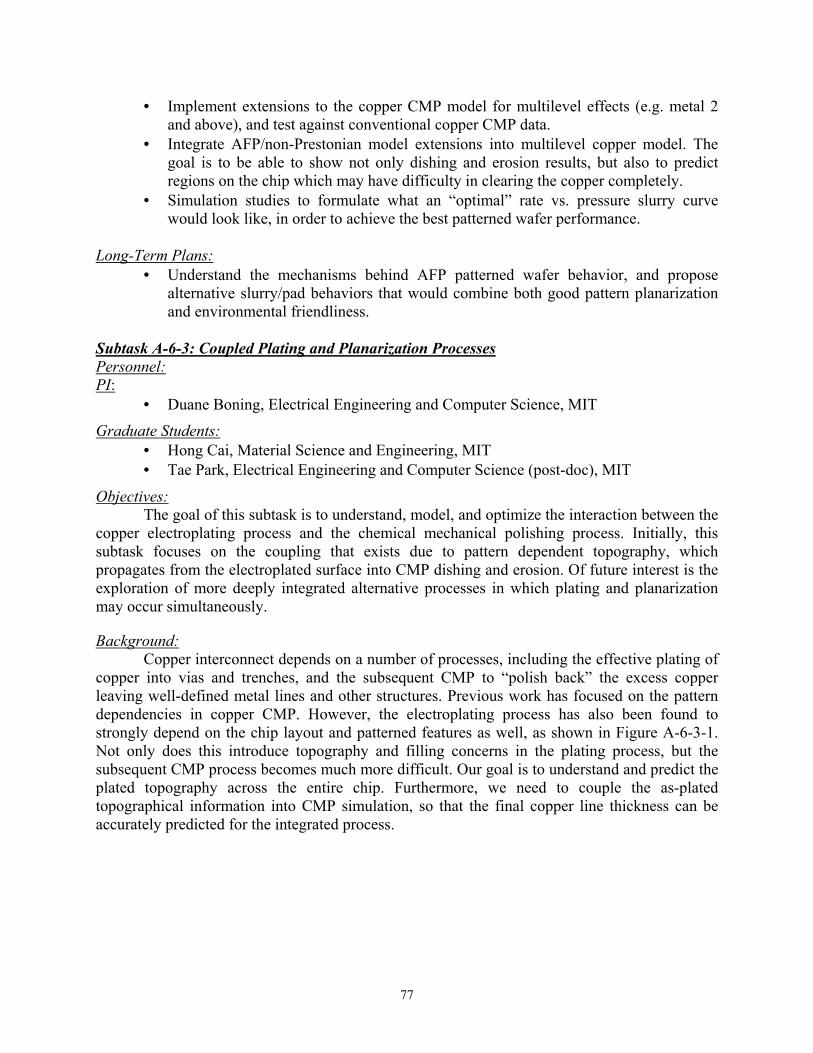
77
• Implement extensions to the copper CMP model for multilevel effects (e.g. metal 2 and above), and test against conventional copper CMP data.
• Integrate AFP/non-Prestonian model extensions into multilevel copper model. The goal is to be able to show not only dishing and erosion results, but also to predict regions on the chip which may have difficulty in clearing the copper completely.
• Simulation studies to formulate what an “optimal” rate vs. pressure slurry curve would look like, in order to achieve the best patterned wafer performance.
Long-Term Plans:
• Understand the mechanisms behind AFP patterned wafer behavior, and propose alternative slurry/pad behaviors that would combine both good pattern planarization and environmental friendliness.
Subtask A-6-3: Coupled Plating and Planarization Processes Personnel: PI:
• Duane Boning, Electrical Engineering and Computer Science, MIT
Graduate Students: • Hong Cai, Material Science and Engineering, MIT • Tae Park, Electrical Engineering and Computer Science (post-doc), MIT
Objectives: The goal of this subtask is to understand, model, and optimize the interaction between the
copper electroplating process and the chemical mechanical polishing process. Initially, this subtask focuses on the coupling that exists due to pattern dependent topography, which propagates from the electroplated surface into CMP dishing and erosion. Of future interest is the exploration of more deeply integrated alternative processes in which plating and planarization may occur simultaneously.
Background: Copper interconnect depends on a number of processes, including the effective plating of
copper into vias and trenches, and the subsequent CMP to “polish back” the excess copper leaving well-defined metal lines and other structures. Previous work has focused on the pattern dependencies in copper CMP. However, the electroplating process has also been found to strongly depend on the chip layout and patterned features as well, as shown in Figure A-6-3-1. Not only does this introduce topography and filling concerns in the plating process, but the subsequent CMP process becomes much more difficult. Our goal is to understand and predict the plated topography across the entire chip. Furthermore, we need to couple the as-plated topographical information into CMP simulation, so that the final copper line thickness can be accurately predicted for the integrated process.
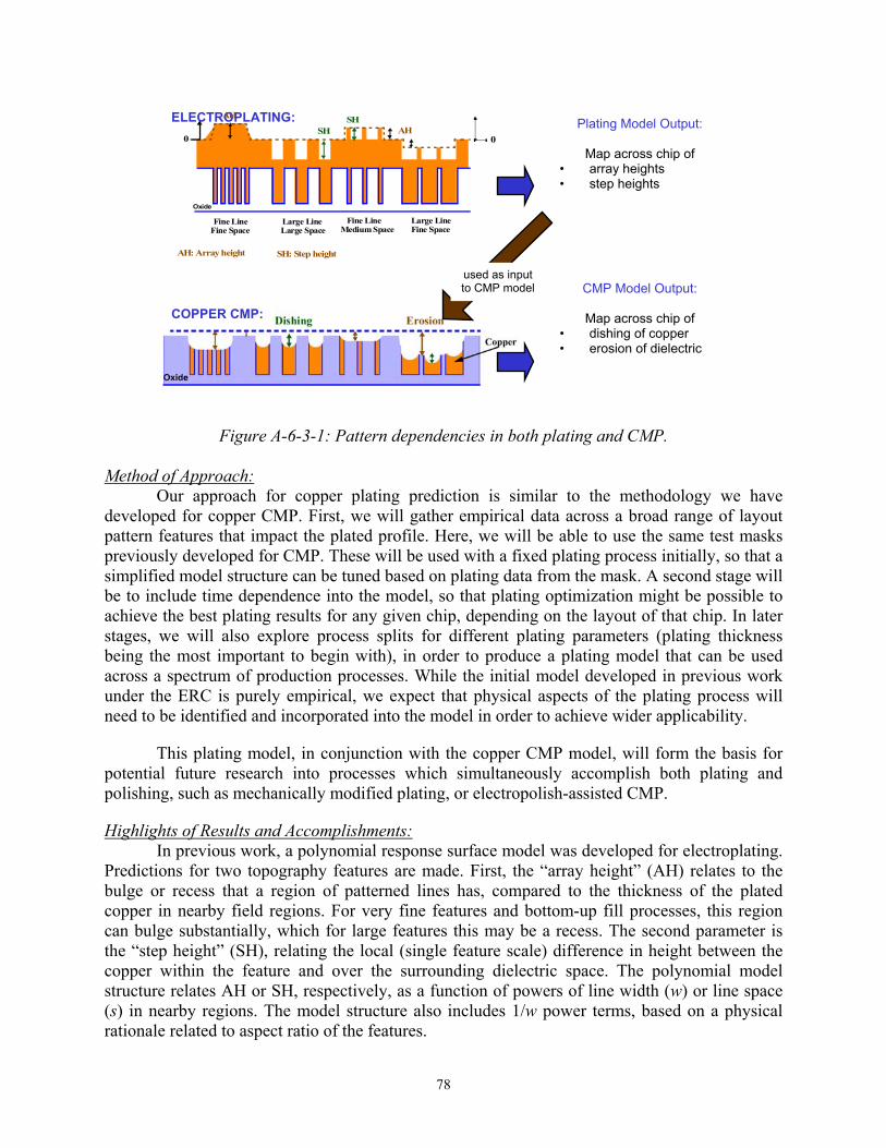
78
Figure A-6-3-1: Pattern dependencies in both plating and CMP. Method of Approach:
Our approach for copper plating prediction is similar to the methodology we have developed for copper CMP. First, we will gather empirical data across a broad range of layout pattern features that impact the plated profile. Here, we will be able to use the same test masks previously developed for CMP. These will be used with a fixed plating process initially, so that a simplified model structure can be tuned based on plating data from the mask. A second stage will be to include time dependence into the model, so that plating optimization might be possible to achieve the best plating results for any given chip, depending on the layout of that chip. In later stages, we will also explore process splits for different plating parameters (plating thickness being the most important to begin with), in order to produce a plating model that can be used across a spectrum of production processes. While the initial model developed in previous work under the ERC is purely empirical, we expect that physical aspects of the plating process will need to be identified and incorporated into the model in order to achieve wider applicability.
This plating model, in conjunction with the copper CMP model, will form the basis for potential future research into processes which simultaneously accomplish both plating and polishing, such as mechanically modified plating, or electropolish-assisted CMP.
Highlights of Results and Accomplishments: In previous work, a polynomial response surface model was developed for electroplating.
Predictions for two topography features are made. First, the “array height” (AH) relates to the bulge or recess that a region of patterned lines has, compared to the thickness of the plated copper in nearby field regions. For very fine features and bottom-up fill processes, this region can bulge substantially, which for large features this may be a recess. The second parameter is the “step height” (SH), relating the local (single feature scale) difference in height between the copper within the feature and over the surrounding dielectric space. The polynomial model structure relates AH or SH, respectively, as a function of powers of line width (w) or line space (s) in nearby regions. The model structure also includes 1/w power terms, based on a physical rationale related to aspect ratio of the features.
ELECTROPLATING:0
Oxide
SH
AH
0
Fine Line Large Line Fine Line Large LineFine Space Large Space Medium Space Fine Space
AHSH
AH: Array height SH: Step height
Plating Model Output:
Map across chip of • array heights • step heights
CMP Model Output:
Map across chip of • dishing of copper • erosion of dielectric
used as input to CMP model
COPPER CMP:

79
The major accomplishment this year is to extend the plating model, to gather new experimental data for plating in collaboration with Hynix Semiconductor, and to validate the model using this new experimental data. As in subtask A6-2, the new experimental data motivated the need to improve the model accuracy before attempting model extensions for time or multilevel structures. Our approach is to generate a semi-physical plating model, retaining the efficient response surface form so that chip-scale simulation can be accomplished, but changing the form of the response based on a physically based model by Josell et al.
In order to explain the superfilling behavior in electroplating with multi-component additives in the bath, Josell proposed a Curvature Enhanced Accelerator Coverage (CEAC) model to explain the bump formation in a specific superfilling recipe [Josell et al., JECS, 148(12), p. 767, 2001]. All adsorbed additives are assumed to float at the surface during deposition. The accumulation of adsorbed accelerator results from reduction of the surface area related to the local surface curvature during growth. At a region of high positive curvature, such as the bottoms of small vias, an increased local velocity is observed. A simple geometrical model reduces the simulation time for any individual feature by capturing the fundamentals of the near-optimized filling mechanics and using a first-order differential equation.
The accumulation of adsorbed accelerator results from reduction of the surface area relative to the local surface curvature during growth, and the local growth velocity is a function of the accumulation of adsorbed accelerator. Thus, we can use w-3/s-3, w-2/s-2, w-1/s-1, const and even w/s terms to express the local curvature, where w is the line width and s is the line space. After time integration of rate into thickness terms considering the geometric evolution, these become w-2/s-2, w-1/s-1, ln(w)/ln(s), w/s and w2/s2, and we can utilize these new model terms to express the as-deposited topography of SH and AH. In deriving model variables that are more physically motivated, the basic electroplating mechanism and superfill mechanism have been examined. By using JMP statistical software, we have found that the following response model is most effective at capturing step height and array height variations:
( ) ( ) ( ) 012 log*log**log*** CswEwDwCwBwASH +++++= −− (3)
( )( ) ( ) 1
111
212
*log*log****
**log***
CDIswHswGsF
wEwDwCwBwAAH
eeee
eeeee
+++++
++++=−−−
−−
(4)
where SH is step height, AH is array height, and D is density. w and s are line width and line space, respectively, and A, B, C, D, E, C0, Ae, Be, Ce, De, Ee, Fe, Ge, He, Ie, and C1, are model coefficients. The important difference in this model, compared to the previous polynomial model, is the inclusion of logarithmic and other terms which are based on the physical model of Josell.
The chip-scale prediction results using the improved copper electroplating model are shown in Figure A-6-3-2. In this case, the root-mean-square errors are 264 Å for the step height, and 181 Å for the array height.

80
Figure A-6-3-2: Left: average feature step height across chip after electroplating (color scale in Å). Right: the resulting raised topography pattern density after
plating. Color scale is in fraction (1.0 represents raised area).
In conjunction with subtask A6-2, this electroplating model is also integrated with the copper CMP model, to achieve coupled plating/CMP simulation. The first step CMP results shown in subtask A6-2 take as input the chip-scale prediction produced using the above model.
Next-Year Plans: • Extend model to accommodate electroplated thickness (or time) as a parameter • Investigate plating pattern dependencies in multilevel copper structures (current
model assumes the starting surface is flat, as in metal 1, only).
Long-Term Plans: • Develop optimization methods for coupled plating/CMP process optimization that
minimize process thickness, process time, and consumable usage. • Investigate pattern and layout dependent models for electropolishing, simultaneous
deposition and planarization of copper, or other alternative processes. Subtask A-6-4: Controlled Atmosphere Planarization and Novel Pad Conditioning Personnel: PI:
• Ara Philipossian, Chemical and Environmental Engineering, UA • Toshiroh Doi, Chemical and Environmental Engineering, UA
Graduate Students:
• Darren DeNardis, Chemical and Environmental Engineering, UA Undergraduate Students:
• Masano Sugiyama, Chemical and Environmental Engineering, UA

81
Objectives:
The main objectives of this subtask are to (1) characterize the mechanism of copper CMP by gaining further insight into the role of various oxidizing species that affect the formation of intermediate copper complex layers crucial for subsequent abrasion, and (2) determine the efficacy of high pressure water micro-jet (HPMJ) technology as an alternative to diamond conditioning in ILD CMP.
Method of Approach, Highlights of Results and Accomplishments:
To fulfill the first objective, a new Controlled Atmosphere Polisher (CAP) manufactured by Fujikoshi Machinery Corporation is used for CMP of copper substrates. The novel tool features a pressure-resistant chamber that hermetically contains the entire processing unit. The machine allows chamber gases to be rapidly changed during polishing. A vacuum pump or a compressor is used to maintain chamber pressure (under vacuum or pressurized conditions) at a desired set point. The apparatus is shown in Figure A-6-4-1.
The objective of this research is to characterize the mechanism of copper CMP by
gaining further insight into the role of various oxidizing species that affect the formation of intermediate copper complex layers crucial for subsequent abrasion. This is achieved by utilizing various high-purity gases such as oxygen, air and nitrogen during polish and by modulating their concentration in the slurry by controlling the chamber pressure. Moreover, the presence or absence of oxidants such as hydrogen peroxide, in conjunction with the above chamber conditions, is expected to shed further light into the complex interplay of various processing parameters on copper removal.
Figure A-6-4-1: Controlled Atmosphere Polisher’s side (left) and top (right) views
In this study, the CAP was used to polish 100-mm copper discs on Rodel IC-1400 k-grooved pads. In all cases, Fujimi’s PL-7102 copper slurry, flowing at 80 cc/min, was used. Wafer pressures and relative pad-wafer velocities ranged from 1.5 to 3.2 PSI, and from 0.26 to

82
0.52 m/s, respectively. First, the effect of chamber pressure was quantified by polishing at 1 and 5 ATM under ultra-pure air conditions. Results are shown in Figure A-6-4-2. In the presence of hydrogen peroxide, chamber pressure had no effect on copper removal rate. At a chamber pressure of 5 ATM, as long as the slurry contained hydrogen peroxide, the type of gas used (i.e. air, nitrogen or oxygen) had no effect on copper removal. This suggested that the concentration of dissolved gaseous species in the slurry (in accordance with Henry’s Law) were insignificant compared to the concentration of oxidizing species associated with hydrogen peroxide.
Figure A-6-4-2: Effect of chamber pressure and chamber gas ambient on copper removal
rate in the presence of hydrogen peroxide containing Fujimi PL-7102 slurry
The feasibility of oxidizing the copper surface (in the absence of hydrogen peroxide) using dissolved gaseous species was investigated by comparing the effect of oxygen and nitrogen chamber gases at 5 ATM. Results are shown in Figure A-6-4-3. Copper removal under oxygen was considerably lower in the absence of hydrogen peroxide compared to cases where hydrogen peroxide was used. However, removal rate was higher by a factor of 4 when oxygen was used instead of nitrogen (in the absence of hydrogen peroxide). This suggests that external sources of
0.0E+00
2.0E-09
4.0E-09
6.0E-09
8.0E-09
1.0E-08
1.2E-08
0.E+00 5.E+03 1.E+04 2.E+04P x U (Pa m/s)
RR
(m/s
)
Fuj (1.01 kPa) w/ H202
Fuj (500 kPa) N2 w/H202
Fuj (500 kPa) O2 w/H202
Fuj (500 kPa) Air w/H202

83
oxygen (especially ones with lower values of Henry’s constant) have the potential of reducing, or even eliminating, the need for hydrogen peroxide for copper polish.
Figure A-6-4-3: Effect of chamber gas ambient on copper removal rate in the absence of hydrogen peroxide (slurry = Fujimi PL-7102)
Regarding the second objective of this subtask, the efficacy of an alternative to diamond
conditioning in the interlayer dielectric (ILD) chemical mechanical planarization (CMP) process was investigated. The High Pressure Micro-Jet (HPMJ) system, manufactured by Asahi Sunac Corporation, was studied to determine if the process could be used as a substitute for, or in conjunction with, conventional diamond disc pad conditioning. The system is designed to jet ultra pure water (UPW), at pressures of 5 to 20 MPa, onto the surface of the pad used for wafer polishing.
In this study, the effect of using the HPMJ system for ex-situ pad conditioning was
analyzed in terms of its tribological and removal rate attributes. The new process was also compared to those of in-situ diamond conditioning, ex-situ diamond conditioning and no conditioning. Experiments were performed on a scaled version of a Speedfam IPEC 472 polisher using IC-1000 perforated pads (no sub-pad) with 100-mm ILD substrates. Fujimi’s PL-4217 slurry (12.5 % weight percent fumed silica abrasives) was used. Slurry flow rate was maintained at 80 cc/min. The variables associated with the HPMJ system included: water jet pressure, nozzle fan angle, actuator angle, water flow rate, distance from the nozzle to the pad, and jet spray time. The effects of actuator angle and jet spray time on coefficient of friction (COF) and removal rate were investigated to optimize the HPMJ system for ILD CMP. Various features of the HPMJ system are shown in Figure A-6-4-4.
The optimal actuator angle and jet time were found to be 25o and 30 seconds. It was
found that using the HPMJ system alone resulted in higher values of COF compared to cases where no conditioning was adopted. However, the HPMJ resulted in removal rates that were similar to cases where pads were not conditioned. Ex-situ diamond conditioning and the HPMJ resulted in similar values of COF but the removal rates associated with the HPMJ were
0.0E+00
5.0E-10
1.0E-09
1.5E-09
2.0E-09
2.5E-09
0.E+00 5.E+03 1.E+04 2.E+04P x U (Pa m/s)
RR
(m/s
)
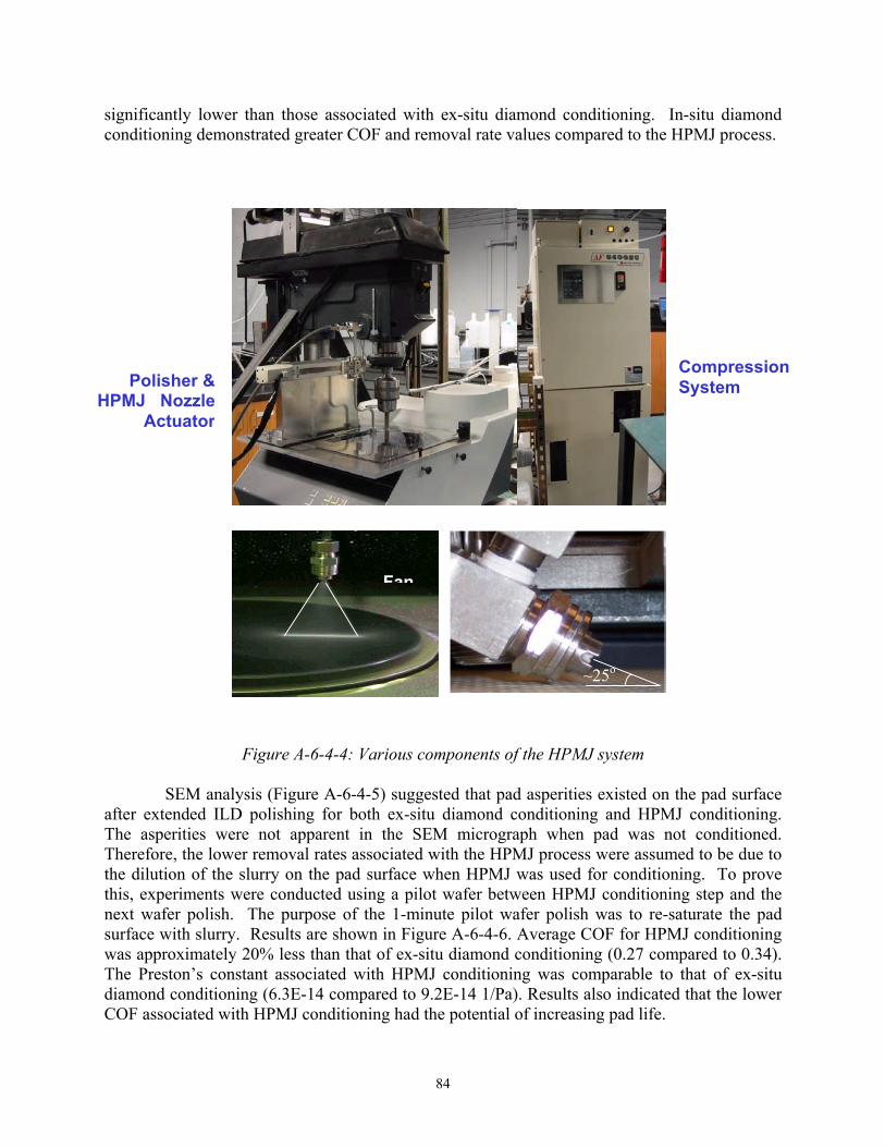
84
significantly lower than those associated with ex-situ diamond conditioning. In-situ diamond conditioning demonstrated greater COF and removal rate values compared to the HPMJ process.
Figure A-6-4-4: Various components of the HPMJ system SEM analysis (Figure A-6-4-5) suggested that pad asperities existed on the pad surface
after extended ILD polishing for both ex-situ diamond conditioning and HPMJ conditioning. The asperities were not apparent in the SEM micrograph when pad was not conditioned. Therefore, the lower removal rates associated with the HPMJ process were assumed to be due to the dilution of the slurry on the pad surface when HPMJ was used for conditioning. To prove this, experiments were conducted using a pilot wafer between HPMJ conditioning step and the next wafer polish. The purpose of the 1-minute pilot wafer polish was to re-saturate the pad surface with slurry. Results are shown in Figure A-6-4-6. Average COF for HPMJ conditioning was approximately 20% less than that of ex-situ diamond conditioning (0.27 compared to 0.34). The Preston’s constant associated with HPMJ conditioning was comparable to that of ex-situ diamond conditioning (6.3E-14 compared to 9.2E-14 1/Pa). Results also indicated that the lower COF associated with HPMJ conditioning had the potential of increasing pad life.
Compression System Polisher &
HPMJ NozzleActuator
Fan
~25o
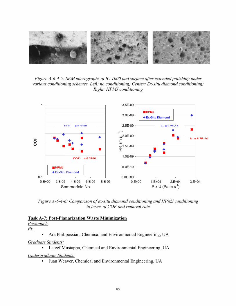
85
Figure A-6-4-5: SEM micrographs of IC-1000 pad surface after extended polishing under various conditioning schemes. Left: no conditioning; Center: Ex-situ diamond conditioning;
Right: HPMJ conditioning
Figure A-6-4-6: Comparison of ex-situ diamond conditioning and HPMJ conditioning in terms of COF and removal rate
Task A-7: Post-Planarization Waste Minimization Personnel: PI:
• Ara Philipossian, Chemical and Environmental Engineering, UA
Graduate Students: • Lateef Mustapha, Chemical and Environmental Engineering, UA
Undergraduate Students: • Juan Weaver, Chemical and Environmental Engineering, UA
0.0E+00
5.0E-10
1.0E-09
1.5E-09
2.0E-09
2.5E-09
3.0E-09
3.5E-09
0.E+00 1.E+04 2.E+04 3.E+04P x U (Pa m s-1)
RR
(m s
-1)
HPMJ
Ex-Situ Diamond
0.1
1
0.E+00 2.E-05 4.E-05 6.E-05 8.E-05
Sommerfeld No
CO
F
HPMJEx-Situ Diamond
COFavg = 0 3398
COFavg = 0.2706
kPr = 9 2E-14
kPr = 6.3E-14
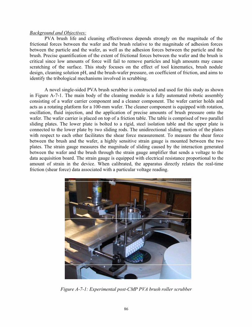
86
Background and Objectives: PVA brush life and cleaning effectiveness depends strongly on the magnitude of the
frictional forces between the wafer and the brush relative to the magnitude of adhesion forces between the particle and the wafer, as well as the adhesion forces between the particle and the brush. Precise quantification of the extent of frictional forces between the wafer and the brush is critical since low amounts of force will fail to remove particles and high amounts may cause scratching of the surface. This study focuses on the effect of tool kinematics, brush nodule design, cleaning solution pH, and the brush-wafer pressure, on coefficient of friction, and aims to identify the tribological mechanisms involved in scrubbing.
A novel single-sided PVA brush scrubber is constructed and used for this study as shown
in Figure A-7-1. The main body of the cleaning module is a fully automated robotic assembly consisting of a wafer carrier component and a cleaner component. The wafer carrier holds and acts as a rotating platform for a 100-mm wafer. The cleaner component is equipped with rotation, oscillation, fluid injection, and the application of precise amounts of brush pressure onto the wafer. The wafer carrier is placed on top of a friction table. The table is comprised of two parallel sliding plates. The lower plate is bolted to a rigid, steel isolation table and the upper plate is connected to the lower plate by two sliding rods. The unidirectional sliding motion of the plates with respect to each other facilitates the shear force measurement. To measure the shear force between the brush and the wafer, a highly sensitive strain gauge is mounted between the two plates. The strain gauge measures the magnitude of sliding caused by the interaction generated between the wafer and the brush through the strain gauge amplifier that sends a voltage to the data acquisition board. The strain gauge is equipped with electrical resistance proportional to the amount of strain in the device. When calibrated, the apparatus directly relates the real-time friction (shear force) data associated with a particular voltage reading.
Figure A-7-1: Experimental post-CMP PVA brush roller scrubber

87
Coefficient of friction (COF) values are determined by dividing the shear force by the
normal force applied onto the wafer. The latter can be experimentally determined by measuring the contact area and the pressure exerted by the brush on the substrate. This is achieved by a automated pressure sensor consisting of two thin sheets. The inner surface of one sheet is patterned in the form of rows while the inner surface of the other employs a columnar pattern. The spacing between rows or columns is approximately 0.5 mm. At each node (i.e. the point where a row intersected a column), an electrical resistance is provided by a thin semi-conductive ink coating, which acts as an intermediate layer between the electrical contacts. When the two polyester sheets are placed on top of each other, a grid pattern is formed, creating a sensing location at each node. By measuring the changes in current flow at each node, the applied force distribution pattern can be measured given a previously obtained calibration graph between current flow and applied pressure. Figure A-7-2 shows the pressure contour plots corresponding to various applied loads onto a noduled PVA brush. Analysis of the repeatability of the COF measurement technique (based on 20 measurements on the same PVA brush as well as 10 measurements each on 10 different brushes) indicates a relative standard deviation of about 5 percent.
Figure A-7-2: Pressure contour plots corresponding to various applied load on the brush
The study consisted of analyzing two designs of PVA brush rollers, manufactured by Rippey Corporation, in terms of their frictional and tribological attributes during post-CMP scrubbing. The two types of brushes were identical to one another in all respects except the first design employed a plurality of nodules on one-fourth of its outer surface while the other did not. The
0.00
0.20
0.40
0.60
0.80
1.00
0 2 4 6 8
Brush-Wafer Contact Area(square inches)
Bru
sh P
ress
ure
(PS
I)
0.25 PSI
0.35 PSI
0.45 PSI
0.58 PSI 0.00
0.20
0.40
0.60
0.80
1.00
0 2 4 6 8
Brush-Wafer Contact Area(square inches)
Bru
sh P
ress
ure
(PS
I)
0.25 PSI
0.35 PSI
0.45 PSI
0.58 PSI

88
inner and outer radii of both types of brushes were identical (the outer radius of the brush with nodules included the 5-mm height of the nodule). Other parameters investigated in this study were the rotational velocity of the roller (10, 20, 30, 40, 50 and 60 RPM), the nominal pH of the cleaning fluid (1.1, 7.0 and 10.7), the type of substrate being scrubbed (blanket silicon dioxide wafer and STI-patterned silicon dioxide wafer), and the applied brush pressure (0.25, 0.35, 0.45 and 0.55 PSI). The particular values of pressure and rotational velocities were selected to mimic conditions typically encountered during industrial PVA brush scrubbing processes. Moreover, a 2-miunte scrubbing process is adopted in this study. This relatively long scrubbing time was critical for ensuring steady state values of COF since during the first 15 seconds COF values were not at steady-state. For a typical 2-minute scrubbing, shear force data were collected at a sampling frequency of 10,000 Hz thus resulting in a total of 1,200,000 force measurements requiring analysis. A relatively high sampling frequency was selected in order to ensure that it is higher than any frequency that may be encountered as a result of the kinematics of the scrubber or the interaction of the brush nodules with the wafers (calculated to be less than 200 Hertz).
Highlights of Results and Accomplishments:
In all cases, higher brush pressures resulted in higher values of COF (Figure A-7-3). Brushes containing nodules showed higher values of COF compared to those without nodules. This difference ranged from 1.5X at low values of pH to about 3X at neutral and high values of pH. COF associated with blanket wafers was statistically the same as those corresponding to STI patterned wafers. This suggested that blanket wafers could act as suitable candidates in establishing the frictional attributes of post-CMP brush scrubbing of typical industrial processes.
Figure A-7-3: Effect of solution pH, brush design and wafer type on COF; solid symbols: brushes without nodules; open symbols: brushes with nodules
1.00E-02
1.00E-01
1.00E+00
STI
Blan
ket
STI
Blan
ket
STI
Blan
ket
STI
Blan
ket
STI
Blan
ket
STI
Blan
ket
CO
F
pH ~ 1.1 pH ~ 7.0 pH ~ 10.7
1.00E-02
1.00E-01
1.00E+00
STI
Blan
ket
STI
Blan
ket
STI
Blan
ket
STI
Blan
ket
STI
Blan
ket
STI
Blan
ket
CO
F
pH ~ 1.1 pH ~ 7.0 pH ~ 10.7

89
This observation was supported by traditional Stribeck curve analysis indicating the absence of ‘boundary lubrication’ throughout the entire range of Sommerfeld numbers employed. Specifically, at low values of pH, regardless of the type of substrate, the tribological mechanism associated with brushes containing nodules was that of ‘partial lubrication’ at higher applied pressures (i.e. 0.55 and 0.45 PSI) and that of ‘hydrodynamic lubrication’ at the lower pressures. At neutral and high values of pH, tribological mechanism was that of ‘hydrodynamic lubrication’ across the entire range of applied pressures and Sommerfeld numbers. Real-time frictional waveforms (in time domain) were further analyzed using spectral techniques to yield information regarding the distribution of the total mechanical energy of the process in frequency domain. The resulting ‘interfacial interaction index’ which was a measure of the total mechanical energy of the process due to stick-slip phenomena, confirmed the tribological results summarized above.
Next-Year Plans:
• Study the effect of PVA brush properties (i.e. porosity, hardness and toughness) on COF and system tribology
• Conduct Fourier transform spectral analysis to determine whether variance analysis of the raw frictional data can shed light on the actual mechanism of wafer scrubbing. Perform these experiments with a variety of cleaning solutions and brush properties
Long-Term Plans:
• Contribute to basic understanding of wafer scrubbing by de-coupling the two widely held mechanisms of capillary suction and brush-wafer abrasion by performing coefficient of friction tests using brush rollers having vastly different porosities.
• Develop physically and chemically based models relating the effect of brush properties on COF and relate the models to recommend improvements to current PVA brush roller designs.
• Develop a model to predict brush life and efficiency to key brush and process attributes and define a cleaning process compatible with next generation ICs.