ti information – selective disclosure. tps65270 peak current mode loop compensation prepared by...
TRANSCRIPT

TI Information – Selective Disclosure.
TPS65270 peak current mode loop compensation
Prepared by Tony Huang
Aug, 2012

TI Information – Selective Disclosure.
Agenda• TPS65270 introduction in brief:
• Peak current mode introduction:
• Peak current control block diagram:
• Peak current mode small signal analysis:
• Design example:
• Conclusion:
• Q&A:

TI Information – Selective Disclosure.
TPS65270 introduction in brief
1. TPS65270 is a dual channel DCDC with peak current mode implementation with integrated synchronous rectifier power FET.
2. TPS65270 has been designed with 5-16V wide input, and loading capability up to 3/2A output currents. Individual SS and EN pins, adj. frequency (300kHz ~ 1.4MHz), Power on sequencer, automatic Power-Save-Mode for light load operations

TI Information – Selective Disclosure.
Peak current mode introduction
• PCM employed a current sampling RAMP to compare with output of the EA(Error amplifier), hereby generate the regulated duty cycle as showed in above Figure.
• PCM benefited the fast response by input or loading transient, with current and voltage loops to realize higher crossover frequency.
.

TI Information – Selective Disclosure.
The overall control block diagram implementation

TI Information – Selective Disclosure.
Buck converter small signal analysis
The average model The Small signal model
The average model and Small signal model.
The gain function from inductor current to output can be got as below:
oLoad
Load
L
Oo CSR
R
SI
SVSR
1)(
)()(
The gain function from duty cycle to inductor current can be got as below:
ooLoad
oLoadILdi LCRSSLR
CSRV
SD
SISH
2
)1(
)(
)()(
)2(1
oLCSL
V
SD
SISH IL
di )(
)()(
Considering the practical crossover frequency is much higher than the corner frequency

TI Information – Selective Disclosure.
Gain functions derivation• The gain function from Vin to inductor current can be got as below:
SL
D
LCSR
LS
DR
SC
SV
SISH
oLoad
Loado
I
Lvi
21
)1
(
)(
)()(
The gain from control to duty cycle can be got as below:
sen TSSFM
)(
1
Sn is the rising slope of the inductor current;Se is the slope compensation rising slope element.Ts is the switching cycle.

TI Information – Selective Disclosure.
Sampling Hold function analysis
• The discrete equation can be derived to describe the sampling-hold behavior:
“Sf” is the inductor current ramp down slope.
. Then, the gain from inductor current to control voltage can be got as below:
)1()1(
1)()1(
^^^
kcRkLKL vii
i
en
ef
SS
SS
Z
Z
RZV
ZIZH
ic
L 1
)(
)()(

TI Information – Selective Disclosure.
Sample hold function analysis
1
2n
eSS
>Based on “Z” domain stability theory, the single pole should meet below condition:
>As a result, the slope compensation element “Se” should meet adequately It’s the criteria for slope compensation:
STse
ST
e
s
STs1
)(
)1(111)(
ST
ST
sis
ST
ST
ST
is
ss
s
s
e
e
STRST
e
e
e
RSH
>With substituting “Z” with “ ” and considering zero order sampling-hold gain , Then:
The below is the gain block description for H(S):
Based on the above block and H(S) function, we can get the sampling hold function He(S) as below:
2
2
)(21
1)(
ss
STs
e
T
S
T
S
e
STSH
s
SL
V
SD
SISH IL
di )(
)()(

TI Information – Selective Disclosure.
Simplify the sample-hold function
Then the simplified schematic can be showed as below
2
2
)(21
1)(
ss
STs
e
T
S
T
S
e
STSH
s
2
22]
2
)([1
11)(
ss
iI
ensi TS
T
RV
SSLTS
RSH
The approximated gain from control to inductor current should be:
The approximate gain from control to inductor current should be:
)11
2(
2
s
e
T
LR
L
TC s
e 2
2
]
2
)1([ s
ei
TD
R
L
L
DF

TI Information – Selective Disclosure.
Verify the model based on TPS65270 PCM(I)
usVu
RL
VS
usVu
RL
VVS
io
f
ioI
n
/048.01.08.6
3.3
/128.01.08.6
)3.312()(
427.0
en
ef
SS
SS
Condition: The frequency is 635kHz, input is 12V and output is 3.3V/2A & 7.7/1A.For channel 2 with 3.3V output:
TPS65270 slope compensation: Se=0.18V/us; Then:
TI Information – Selective Disclosure.
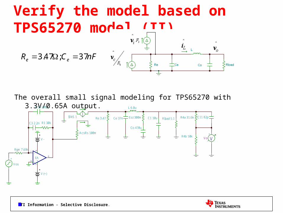
Verify the model based on TPS65270 model (II)
The overall small signal modeling for TPS65270 with 3.3V/0.65A output.
nFCR ee 37;47.3
-
+ +3
2
6
74
EA
Rgm 7.69k
C3 2.2n
V-
+
Vos
V+
Vo
ISNS 1
Co 470u
Rload 5.1R1 30k
C16 100p
AcsRs 100m
R4a 31.6k
R4b 10k
C11 82p
L 6.8u
Re 3.47 Ce 37n
V(+)
Esr 300m C1 10u

TI Information – Selective Disclosure.
Verify the model based on TPS65270 model (III) Well Matched
T
Ga
in (
dB
)
-60.00
-40.00
-20.00
0.00
20.00
40.00
60.00
80.00
Frequency (Hz)
10 100 1k 10k 100k 1M
Ph
ase
[d
eg
]
-200.00
-100.00
0.00
100.00
200.00
AC simulation results revealed a 58degree phase margin and 80kHz crossover frequency.
Lab test results:
The loop parameters can be got as 86kHz crossover frequency and 60degree phase margin.

TI Information – Selective Disclosure.
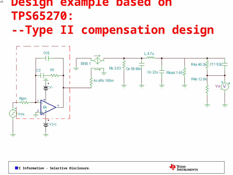
Design example based on TPS65270:
Vin(V) Vout(V) L(uH) f(kHz) Ri Se(V/us)
12 3.3 4.7 600 0.1 0.18
Sn(V/us) Sf(V/us) Re Ce(nF)
0.19 0.07 -0.30 3.03 59.88
Topic: Vin=12V; Vout=3.3V@2A; fs=600kHz; L=4.7uH
V+
Vo
ISNS 1
Co 22u Rload 1.65
AcsRs 100m
R4a 40.2k
R4b 12.8k
C11 82p
L 4.7u
Re 3.03 Ce 59.88n
+
Vc
The small signal modeling from control to output:
TI Information – Selective Disclosure.
Design example based on TPS65270:--Type II compensation design

TI Information – Selective Disclosure.
Design Example based on TPS65270:
• Without compensation, the loop simulation is below:
T
Gai
n (d
B)
-50.00
-40.00
-30.00
-20.00
-10.00
0.00
10.00
Frequency (Hz)
10 100 1k 10k 100k 1M
Phas
e [d
eg]
-300.00
-200.00
-100.00
0.00
a
b
77)50(;87.6)50( kHzPhasedBkHzG coco

TI Information – Selective Disclosure.
Design example based on TPS65270
1. Assuming a crossover frequency “fc”=50kHz.
Let:
And:
2. Then: C16=52.9pF; Select C16=56pF
3. select C3=560pF;
45.010)2( 20
9.6
cco fjGA 5.3)452
90)78(70(
tgK
ku
RCRfA
Kgm
gmc
69.7130
1;
2
1
16
kfC
KR
c
8.182 3
1
pFCKC 590)1(3 162

TI Information – Selective Disclosure.
Design example based on TPS65270:
Target compensation results:Phase margin=70degree; Crossover frequency=50kHz
Employing type II compensation:C16=56pF; C3=560pF; R1=18.8k
-
+ +3
2
6
74
EA
Rgm 7.69k
C3 560p
V-
+
Vos
V+
Vo
ISNS 1
Co 22u Rload 1.65R1 18.8k
C16 56p
AcsRs 100m
R4a 40.2k
R4b 12.8k
C11 82p
L 4.7u
Re 3.03 Ce 59.88n
V(+)

TI Information – Selective Disclosure.
Design example based on TPS65270:• Simulation results: The final crossover frequency is 49kHz and phase margin is 69degree.
T
Gai
n (d
B)
-80.00
-60.00
-40.00
-20.00
0.00
20.00
40.00
60.00
80.00
Frequency (Hz)
10 100 1k 10k 100k 1M
Pha
se [d
eg]
-200.00
-100.00
0.00
100.00
200.00
a
b
TI Information – Selective Disclosure.
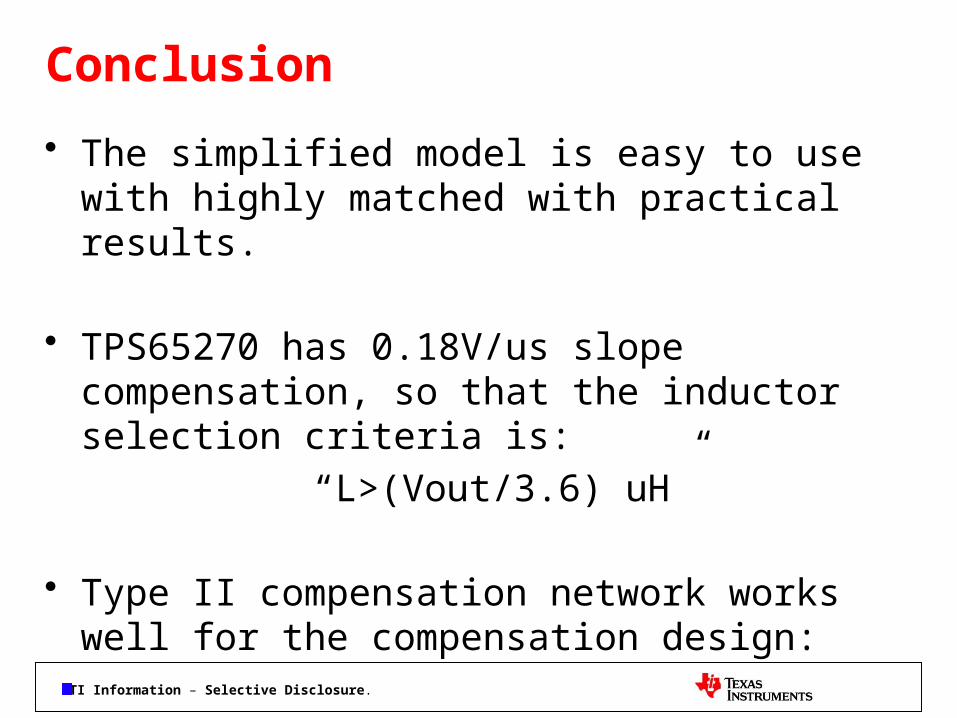
Conclusion
• The simplified model is easy to use with highly matched with practical results.
• TPS65270 has 0.18V/us slope compensation, so that the inductor selection criteria is:
“L>(Vout/3.6) uH”
• Type II compensation network works well for the compensation design:

TI Information – Selective Disclosure.
• Thanks very much for you time!
• Q&A?