timing calibration for up-converting dac · arash azimirad timing calibration for up-converting dac...
TRANSCRIPT

Arash Azimirad
Timing calibration for up-converting DAC
School of Electrical Engineering
Thesis submitted for examination for the degree of Master of
Science in Technology.
Espoo 22.01.2015
Thesis supervisor:
Prof. Jussi Ryynänen
Thesis advisors:
D.Sc. (Tech.) Kari Stadius
M.Sc. (Tech.) Jerry Lemberg

aalto university
school of electrical engineering
abstract of the
master's thesis
Author: Arash Azimirad
Title: Timing calibration for up-converting DAC
Date: 22.01.2015 Language: English Number of pages: 6+50
Department of Micro- and Nanosciece
Professorship: Electrical Circuit Design Code: S-87
Supervisor: Prof. Jussi Ryynänen
Advisors: D.Sc. (Tech.) Kari Stadius, M.Sc. (Tech.) Jerry Lemberg
This thesis deals with the timing error problem that appears in high frequencyDigital to Analog Converters. Inequalities among signal paths in dierent branchesand inaccuracies happened during fabrication, result in dierent time delays indierent branches of a Digital to Analog Converter. The consequence of thisinequality is having the data for dierent bits not arriving to the summationpoint at the same time. This timing error will create some glitches in the outputanalog signalA new approach is introduced in this work that measures the timing error amongbranches of the DAC and corrects them through a calibration process. Being allthe error measurement and its correction process done on chip, this approach cancorrect the errors created by both sources. This idea was implemented and testedin Eldo simulator. A timing error of 8pS was inserted to the MSB branch of a10-bit binary coded DAC. After performing the calibration process on this DAC,the SFDR of the output signal was increased by about 3.2dB.
Keywords: timing error, RF-DAC, DAC, timing calibration, up-converting DAC

iii
Preface
This work has been done at Aalto University, department of Micro- and Nanoscience.It was an independent student project.
I would like to thank Professor Jussi Ryynänen for his supervision over my thesis.Also, my thanks go to Kari Stadius for his instructions during dierent phases ofthe thesis. In addition, I would like to thank Jerry Lemberg for his helpful advicesand consultations about dierent details of the work.
Finally, I would like to thank all people without help of whom it was not possibleto get this work done.
Otaniemi, 22.01.2015
Arash Azimirad

iv
Contents
Abstract ii
Preface iii
Contents iv
Symbols and abbreviations vi
1 Introduction 1
2 Digital to Analog Converters, basic techniques and denitions 4
2.1 Ideal DAC . . . . . . . . . . . . . . . . . . . . . . . . . . . . . . . . . 42.1.1 Non Return-to-Zero DAC . . . . . . . . . . . . . . . . . . . . 42.1.2 Return-to-Zero DAC . . . . . . . . . . . . . . . . . . . . . . . 72.1.3 Nyquist-Shannon sampling theory . . . . . . . . . . . . . . . . 8
2.2 DAC topologies . . . . . . . . . . . . . . . . . . . . . . . . . . . . . . 82.2.1 Resistor DAC . . . . . . . . . . . . . . . . . . . . . . . . . . . 92.2.2 Capacitor DAC . . . . . . . . . . . . . . . . . . . . . . . . . . 92.2.3 Current steering DAC . . . . . . . . . . . . . . . . . . . . . . 10
2.3 Techniques for improving performance of DACs . . . . . . . . . . . . 102.3.1 Dierential topology . . . . . . . . . . . . . . . . . . . . . . . 102.3.2 Thermometer coding . . . . . . . . . . . . . . . . . . . . . . . 122.3.3 Noise Shaping . . . . . . . . . . . . . . . . . . . . . . . . . . . 142.3.4 Deglitching . . . . . . . . . . . . . . . . . . . . . . . . . . . . 152.3.5 Delta-Sigma DAC . . . . . . . . . . . . . . . . . . . . . . . . . 162.3.6 Dynamic Mismatch Mapping . . . . . . . . . . . . . . . . . . . 17
2.4 Denition of performance gures . . . . . . . . . . . . . . . . . . . . 192.4.1 Static accuracy . . . . . . . . . . . . . . . . . . . . . . . . . . 192.4.2 Dynamic accuracy . . . . . . . . . . . . . . . . . . . . . . . . 21
3 Solutions 24
3.1 Introduction . . . . . . . . . . . . . . . . . . . . . . . . . . . . . . . . 243.2 Timing error detector unit . . . . . . . . . . . . . . . . . . . . . . . . 25
3.2.1 Theory . . . . . . . . . . . . . . . . . . . . . . . . . . . . . . . 253.2.2 Simulation results . . . . . . . . . . . . . . . . . . . . . . . . . 30
3.3 Delay unit . . . . . . . . . . . . . . . . . . . . . . . . . . . . . . . . . 31
4 Implementation and simulation results 34
4.1 Implementation . . . . . . . . . . . . . . . . . . . . . . . . . . . . . . 344.2 Calibration process and simulation results . . . . . . . . . . . . . . . 37
5 Conclusions 43
6 Appendix A- Dynamic ip-ops 44

v
7 Appendix B- Comparison between the output of RF-DAC trans-
mitter and DCT 47

vi
Symbols and abbreviations
Symbols
δK Dirac sequencefCLK Frequency of Clock signalfLO Frequency of Local oscillatorT Period
Abbreviations
ADC Analog to Digital ConverterCLK ClockDAC Digital to Analog ConverterDCT Direct Conversion TransmitterDMM Dynamic Mismatch MappingDNL Dierential Non-LinearityEfm,i Non-linearity error of the fundamental component at the i inputEfm,code Integral non-linearity error of the fundamental component at an input codeE2fm,i Non-linearity error of the second harmonic component at the i inputE2fm,i Integral non-linearity error of the second harmonic component at an input codeFS Full ScaleFSR Full Scale RangeFUNDactual The actual fundamental component of the DAC outputFUNDideal The ideal fundamental component of the DAC outputHC2ideal The ideal second harmonic component of the DAC outputHC2actual The actual second harmonic component of the DAC outputIC Integrated CircuitINL Integral Non-LinearityLO Local (signal/carrier)LSB least Signicant BitMSB Most Signicant BitNRZ Non Return to ZeroNTF Noise Transfer FunctionOSR Over Sampling RatioPA Power AmplierPSD Power Spectral DensityRF Radio FrequencyRF-DAC Radio Frequency Digital to Analog ConverterRZ Return to ZeroSFDR Spurious Free Dynamic RangeSNR Signal to Noise RatioZOH Zero Order Hold

1
1 Introduction
Transmitters were classically designed as depicted in Figure 1 [1]:
DA
DA
PA900
I
Q
fLO
Figure 1: Direct Conversion Transmitter (DCT)
This kind of transmitter is called Direct Conversion Transmitter (DCT). As wecan see, the digital data is converted to analog at the baseband and then, afterltering, that analog data is up converted by mixer.
About 10 years ago in [2] a new architecture called RF-DAC was introduced asa replacement for DCT [1]. Since that time various versions of RF-DAC have beendesigned. The general structure of a RF-DAC can be illustrated as in Figure 2:
PA90
0
I
Q
Phase
Shifter
Phase
Shifter
DA
Figure 2: RF-DAC Transmitter
The input digital data is given to the transmitter with the frequency at which wewant to send the signal to the air, i.e., the carrier frequency. So, there is no need forup-conversion (for reading about the draw back of RF-DAC transmitter comparedto DCT, refer to Appendix B). Then after creating a 90-degree phase dierencebetween the I and Q signals, they are added up together to make a unique digitalsignal. Then this signal is converted to analog.
We can see that the DACs used in RF-DAC transmitters work at frequenciesmuch higher than the ones used in DCTs. This fact forces us to deal with a problem

2
called "Timing errors in DACs". Before continuing this argument, it is better torst explain what exactly this problem is. In Figure 3 the general structure of aDAC is illustrated:
D/A
D/A
D/A
+
b1
b2
bn
OUT
Figure 3: The general structure of a DAC
The output of this DAC in the ideal case will be as follows (assuming that thesignal is a ramp, for example):
VOUT
t
Figure 4: The output of an ideal DAC to a ramp input
However, in practice the signals at the branches of dierent bits of the DACdo not move forward simultaneously, due to dierent delays that they face in theirpaths (the source of these delays are factors like dierent path lengths, errors istransistor sizing during fabrication process, ...). These delays are modeled in thediagram of Figure 5:

Delay1
Delay2
Delayn
+ OUT
D/A
D/A
D/A
b1
b2
bn
Figure 5: The realistic model of a DAC
There will be some glitches in the output of this DAC at the transition points ofthe signal, as illustrated in Figure 6:
VOUT
t
Figure 6: The output of a real DAC
Because the delay times are small, the frequency of these glitches are high. So,for the DACs not operating at high frequencies, these glitches are not a big problemand can be easily ltered out at the output. But, as the operating frequency of theDAC grows, ltering these glitches becomes more dicult.
Now, returning back to our earlier discussion about DCTs and RF-DAC trans-mitters, the DACs in the RF-DAC transmitter architecture usually deal with timingerror problem. And as this structure is becoming more popular, the need for solu-tions for this problem is becoming more serious.
The object of this thesis is nding solutions for the timing error problem in RF-DACs. In this thesis we do not go through the design of the whole transmitter andjust focus on the RF-DAC itself. The results can be useful for high-speed DACswhich are used for applications other than transmitters, as well.
4
2 Digital to Analog Converters, basic techniques
and denitions
In this section some basic concepts and denitions about Digital to Analog Con-verters are explained.
2.1 Ideal DAC
Any digital code can be expressed as follows [3]:
d =B−1∑
i=0
2i.bi bi ∈ [0, 1] (1)
By multiplying Equation 1 to a constant value like ∆ we will have:
u = ∆.B−1∑
i=0
2i.bi (2)
This equation is the basis of the operation of Digital to Analog Converters. Thevalues of the terms ∆.2i are created either by voltage or current or electrical charge.Usually a reference source with the value of ∆ is used for creating dierent ∆.2i
terms. The operation of the terms bi is realized by the use of switches. We can seethat equation 2 can take on only some specic discrete values. The step size betweentwo consequent values is∆. It means that if we want to convert an analog signal withits amplitude between uk = ∆.2k and uk+1 = ∆.2k+1 to digital, we should chooseone of the values uK and uk+1. This unavoidable error created due to the digital toanalog conversion is called "Quantization error". The value of quantization error isbetween −1
2∆ and +1
2∆.[3]
Another term dened for DACs is Full Scale Range (FSR). It shows the maximumamplitude that the DAC can sweep in its output. Considering equation 2, we canderive the relation for FSR as follows [3]:
FSR = u|b0,b1,...,bB−1=1−u|b0,b1,...,bB−1=0 = ∆.
B−1∑
i=0
2i.1−∆.
B−1∑
i=0
2i.0 = ∆.(2B−1) (3)
2.1.1 Non Return-to-Zero DAC
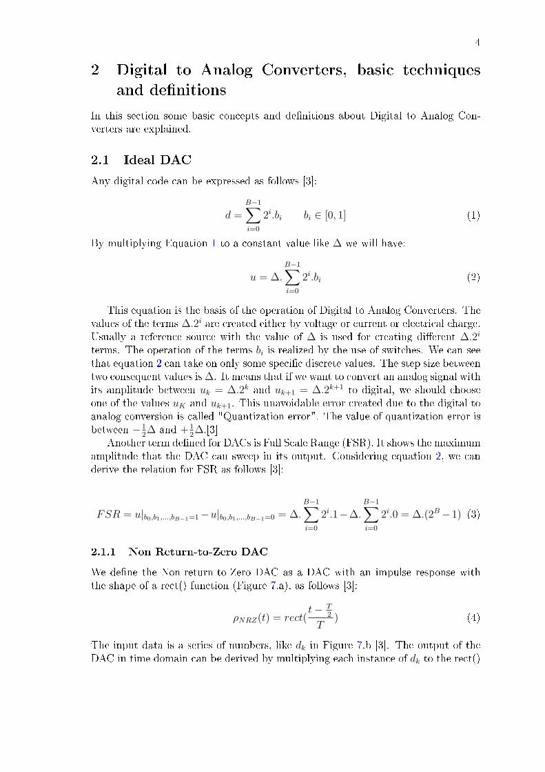
We dene the Non-return-to-Zero DAC as a DAC with an impulse response withthe shape of a rect() function (Figure 7.a), as follows [3]:
ρNRZ(t) = rect(t− T
2
T) (4)
The input data is a series of numbers, like dk in Figure 7.b [3]. The output of theDAC in time domain can be derived by multiplying each instance of dk to the rect()
5
k
k dk
k
t
uNRZ(t)CLK
T
y.LSB1.LSB
Tt
y1
ρNRZ(t)
a b
Figure 7: Ideal NRZ DAC input and output: (a) impulse response (b) typical digitalinput and the output of the DAC for it
function of 4 [3]:
uNRZ(t) =∑
k
dk.uNRZ(t− k.T ) =∑
k
dk.rect(t− k.T − T
2
T) (5)
For investigating the output of the NRZ-DAC in frequency domain, we should cal-culate the Fourier transform of 5. Equation 5 can be written as follows [3]:
uNRZ(t) = [d(t).∑
k
δ(t− k.T )] ∗ ρNRZ(t) (6)
Now for calculating the fourier transform of 5 we can multiply the fourier transformof each of the expresssions on the sides of the convolution sign in 6. The fouriertransform of ρNRZ(t) is:
ρNRZ(t) = rect(t− T
2
T) ⇒ ρNRZ(jω) = T.
sinωT2
ωT2
.e−jωT
2 (7)
So, the fourier transform of 6 will be [3]:
UNRZ(jω) =1
T
∑
m
D(j(ω −m2π
T)).ρNRZ(jω) (8)
|UNRZ(jω)| and also |D(jω)| and |ρNRZ(jω)| are drawn in Figure 8 [3]. The fre-quency response of the NRZ-DAC is a sinc() function with zeros at even multiplesof 2π
T.

6
|D(j)|
2T T
a
b
c
|D(j-jm )|
|NRZ(j)|
|UNRZ(j)|1st Nyquist band
2nd Nyquist band
3rd Nyquist band
-
T
T-
T
T-
T-
2T
-
2T
2T
2T
2T
-
2Tm
Figure 8: Spectrum of ideal NRZ DAC: )a (repetitive) input spectrum, (b) NRZDAC unit pulse spectrum, (c) NRZ DAC output spectrum

7
2.1.2 Return-to-Zero DAC
π
T
2π
T
2π
TS
ω
|ρRZ(jω)|
πT
2πT
3πT
2πTS
ω
|URZ(jω)|
1st Nyquist band2nd Nyquist band
3rd Nyquist band
tTS T 2T
uRZ(t)
C
b
a
Figure 9: Spectrum of ideal RZ DAC: (a) ideal time domain output waveform (b)RZ DAC unit pulse spectrum (c) RZ DAC output spectrum
The time response of the Return-to-Zero (RZ) DAC is illustrated in Figure 9a[3]. We can see that the width of the pulse is equal to a portion of the samplingperiod. We call the fraction of TS
T"Duty factor" and show it with D. For getting

8
the frequency response of RZ-DAC we should change T in Equation 7 to TS [3]:
ρRZ(t) = rect(t− TS
2
TS
) ⇒ ρRZ(jω) = TS.sinTS
2
ωTS
2
.e−jωTS
2 (9)
Continuing in a manner similar to what we did for NRZ-DAC, we can get thefrequency response of RZ-DAC to a series of digital inputs, as follows:
URZ(jω) =1
T
∑
m
D(j(ω −m2π
T)).ρRZ(jω) (10)
The transfer function of the RZ-DAC and its output in frequency domain areillustrated in gures 9b and 9c. The transfer function of RZ-DAC, similar to NRZ-DAC, is a sinc(); With this dierence that its zeros are at even multiples of 2π
TS, not
2πT. It means that its rst zero is at bigger frequency, compared to NRZ-DAC. This
will lead to less amplitude distortion [3]. However, the main reason for preering RZ-DAC to NRZ-DAC in some applications, is due to its better dynamic performance.This feature is based on its hardware implementation [3]. But, this advantage comeswith the drawback of having the the power of the base band signal weakened by thefactor of (TS
T)2 (compared to NRZ-DAC) [3].
2.1.3 Nyquist-Shannon sampling theory
Nyquist-Shannon sampling theory is one of the fundamental theories about Analogto Digital and Digital to Analog conversion. It can be explained as follows:
The minimum sampling frequency that is needed for sampling an analog signalwith highest frequency component of fH , in order to be able to reconstruct it fromthe samples later, without any data loss, is 2fH . [4]
The frequency 2fH is called the Nyquist frequency."Aliasing" and "Over sampling" are two terms about sampling which are related
to Nyquist frequency. They are dened as follows:
2.1.3.1 Aliasing If we have component with a frequency over Nyquist frequencyat the input of an ADC, they will be folded back or replicated at frequencies above orbelow the Nyquist frequency. This phenomena is called "Aliasing". For preventingthis issue, proper ltering should be done before giving the signal to the ADC [5].
2.1.3.2 Over sampling If we sample analog signal at frequencies much higherthan Nyquist frequency, we have "oversampled" it. Oversampling decreases quanti-zation noise and improves signal quality [5].
2.2 DAC topologies
There are three main topologies used for implementing DACs. They are brieyexplained in the following parts.

9
2.2.1 Resistor DAC
This is the most simple implementation of DACs. In Figure 10 [6] a form of thistopology called R-2R ladder is illustrated:
Vout
R
2R2R2R2R2R2R
RRRR
Vref
b0b1b2b3b4
Figure 10: 5-bit R-2R ladder DAC
By changing the position of the bit switches, we can make all the analog voltagescorresponding to dierent binary input codes.
For getting nice accuracy the ratio of resistors should be implemented accurately.Non linearities of the resistors and the buer and also the buer bandwidth and thelarge RC time constant of this topology degrade its linearity and speed. So, thisstructure is not convenient for high speed conversion applications. [6]
2.2.2 Capacitor DAC
Vout
Vref
Cf
C2C4C8C16C
b0b1b2b3b4
Figure 11: 5-bit switched capacitor DAC
You can see the schematic of this topology in Figure 11 [6]. The conversionis performed in two phases; In the rst phase, the binary capacitors are connectedeither to the reference voltage or to ground, based on the value of their correspondingbits. In this phase the feedback capacitor is shorted. In the second phase, allthe input switches connect one end of all binary capacitors to ground, and theswitch around the feedback capacitor opens. In this way, the charge that all binarycapacitors had gathered during the rst phase, will be transfered to the output.

10
The advantage of this topology is it's low power consumption. Similar to resis-tor DAC, the accuracy of the DAC depends on the accuracy of the values of thecapacitors. Although it is faster than resistor DACs, but still speed and linearityare the main problems in this structure. [6]
2.2.3 Current steering DAC
+ Vout -
b0b1b2b3b4
I2I4I8I16I
RL RL
Figure 12: 5-bit current steering DAC
The general structure of a ve bit binary coded dierential current steering DACis illustrated in Figure 12 [6]. The currents corresponding to dierent input bits willbe added up together at the output node and change to voltage by owing to theload resistance.
The acceptable performance of current steering DACs at high frequencies hasmade them the only practical choice in such applications [7]. Another advantage ofthis topology is having high output impedance and also having the output signal inthe form of current. Due to this feature they can drive a 50Ω standard load withoutthe need for buer. [6]
2.3 Techniques for improving performance of DACs
2.3.1 Dierential topology
Dierential topology is usually preferred to single ended topology due to its betternoise performance. In the dierential topology the common mode noise will beeliminated. A single ended 10 bit DAC and a dierential 10 bit DAC are illustratedin gures 13 and 14, respectively:

11
X1B0X2B1X4B2X512B9
VDD
RL
Vout
Figure 13: Single ended 10 bit DAC
D Q
Q
Io
Io
D Q
Q
Io
Io
D Q
Q
Io
Io
D Q
Q
Io
Io
B0
B1
B2
B9
X2
X4
X512
VDD VDD
RL RL
Vout
Vout
+_
D Q
Q
Io
Io
Circuit diagram of the above blocks:
Figure 14: Dierential 10 bit DAC

12
We can see that in the dierential case, both nodes of the output are branchedfrom signal line. It means that the noise existing on the input signal will be on bothnodes of the output which will result in them canceling out each other. While it isnot the case in the single ended mode. [1]
2.3.2 Thermometer coding
Thermometer coding or unary coding is a coding system for showing zero and naturalnumbers with 1s and 0s. This coding system for numbers 0 to 5 is described in Table1:
Number Thermometer code0 01 102 1103 11104 111105 111110
Table 1: Thermometer coding
This coding system changes the "rising and falling edge" glitches at the outputof a binary coded DAC, produced due to the dierence between "switching o"and "switching on" times of a transistor, to "just rising edge" or "just falling edge"glitches (depending on whether the signal value is increasing or decreasing).
For clarifying this issue, we consider the output of a binary coded DAC and alsoa thermometer coded DAC when their input data changes from the value of 2 to 5.In this example we imagine the "switching on" delay time of a transistor to be 2time units and its "switching o" time to be 1 time unit.
In the binary coded DAC this transition will be from the code "010" to the code"101". The implementation of this transition in the related circuit is illustrated inFigure 15:
B2 B1 B0
X4 X2 X1
B2 B1 B0
X4 X2 X1
VDD VDD
RL RLVout Vout
Figure 15: Transition from 2 to 5 in a binary coded DAC

13
Considering the delay times we dened above, the output wave of the DAC willbe as follows:
2
5
1 2time
Vout
0
Figure 16: Output of the circuit in Figure 15
Now we consider this transition in a thermometer coded DAC. Thermometercode for 2 is "110" and for 5, it is "111110". Implementation of this transition inthe circuit is illustrated in Figure 17:
B0B1B2B3B4B5
X1
RL
VDD
Vout
X1X1X1X1X1
B0B1B2B3B4B5
X1
RL
VDD
Vout
X1X1X1X1X1
Figure 17: Transition from 2 to 5 in a thermometer coded DAC

14
By considering the delay times we dened above for transistor switching times,the output wave of this DAC will be as follows:
2
5
1 2time
Vout
0
Figure 18: Output of the circuit in Figure 17
By comparing the waveforms of gures 16 and 18 we can see that the risingand falling edge glitches have changed into "just rising" glitches thanks to the ther-mometer coding. However, this advantage of thermometer coding comes with thedrawback of more IC area consumption, and also more complex control signals.
2.3.3 Noise Shaping
The spectrum of the quantization noise of a DAC is normally as depicted in Figure19 [3]:
Sq(j)
ffCLK22
fCLK12
Δ2
12Δ2
12
Δ2
12
fCLK1
2
fCLK2
2
Figure 19: Quantization noise of Nyquist rate DAC
By means of some techniques, called "Noise Shaping", we can change the quan-tization noise spectrum of Figure 19 to something like Figure 20 [3]:

15
Sq(j)
ffCLK
2
2
12
fB
fCLK
2
2
12
NTF(f)
in-band noise
Figure 20: Noise shaped quantization noise
As we can see in Figure 20, the quantization noise at desired frequency hasdecreased signicantly. And it has become much larger at out-of-band frequencies.
Noise shaping idea was rst introduced by Cutler [8] in 1954 [9].
2.3.4 Deglitching
As explained in Introduction chapter, the timing error in DACs creates some glitchesat the output of the DAC, as it was illustrated in Figure 6. One solution for overcom-ing this problem is "Deglitching". In this approach a unit called "track-and-hold"(T&H) is inserted between the output of the DAC and the output node. As illus-trated in Figure 21 [10], there is a switch in T&H unit which can connect/disconnectthe output of the DAC to/from the output node, by a control voltage. Also, a stor-age unit (like a capacitor) is connected at the output node in order to reserve (hold)the voltage of the output node, after the switch gets open.
DAC
T&HInput
Data
DAC
Output
VControl
VOut
Figure 21: DAC and T&H unit

16
In Figure 22 [10], we can see the wave forms of the voltages of dierent nodes ofFigure 21. The control voltage consists of two phases; Track phase and Hold phase.During Track phase the switch connects the output of the DAC to the output node.This phase should start after the glitches at the output of the DAC are settled downand it should nish before the glitches of the next cycle have started. During theHold phase the switch gets open. This phase starts before the glitches happen atthe output of the DAC, and it nishes after those gliches are settled down. Duringthis phase the output node reserves its previous voltage until the next Track phasebegins. As illustrated in Figure 22, through this approach we can prevent the glitchesat the output of the DAC from appearing at output node. However, implementingthe phases of the control voltage requires special care. In addition, distortion andnoise of T&H can aect the performance of the DAC [10].
Input
Data
DAC
Output
VControl
VOut
T H T H T H T H T H
Figure 22: Waveforms of the circuit of Figure 21
2.3.5 Delta-Sigma DAC
Delta-Sigma is a modulation technique which is used in many electronic circuits,including DACs. A Delta-Sigma modulator converts an analog signal to a streamof bits. At each sample moment, instead of converting the analog signal amplitudeto a digital code, it calculates the dierence (Delta) of the current sample with theprevious one. For making the original analog signal from these bits, we should add(Sigma) them together [11].
There are several motivations for using Delta-Sigma modulators in DACs; Delta-Sigma DACs have lower quantization noise in desired frequencies. The use of Delta-Sigma modulators in DACs results in cheaper circuitry with less power consumption[12]. If we want to achieve the resolution that we get with a Delta-Sigma DAC, witha conventional DAC, we should use much more accurate analog components [13].
Figure 23, taken from [14], shows the diagram of a typical Delta-Sigma DAC.

17
Interpolation
Filter
Delta-Sigma
Modulator
1-Bit
DAC
Output
Filter
Digital
Input
Signal
Up-Sampled
SignalBit Stream Analog Signal
(containg noise)Analog
Output
Signal
Figure 23: Diagram of a typical Delta-Sigma DAC
The output of Delta-Sigma modulator is one stream of 1s and 0s. But, theinput digital signal to this Delta-Sigma DAC, consists of several of such streams(depending on the bit-count of the DAC). So, it means that in order to not looseany data we need to have the sample rate of Delta-Sigma modulator output be muchmore than the sample rate of input digital code. This increase in sample rate is doneby help of an interpolation lter. Interpolation lter rst inserts a xed amount ofzeros (depending on amount of desired increase in sample rate) between each twoconsequent samples. Then by passing the resulted signal through a low-pass lter,the zeros will become interpolated. Sigma-Delta modulator produces a stream ofbits. For each sample at the digital input, there is a xed number of bits at theoutput of Delta-Sigma modulator. We have a 1-bit DAC at the output of Delta-Sigma modulator that converts the bit stream to an analog signal. The producedanalog signal contains the data of the input signal in its baseband and most ofthe quantization noise and the image of the input signal at higher bands. So, forextracting data a low pass lter is needed at the output, as illustrated in Figure 23[14].
2.3.6 Dynamic Mismatch Mapping
Dynamic Mismatch mapping (DMM) is a new approach introduced in [6]. Two newparameters called Dynamic-DNL and Dynamic-INL are dened as follows:
dynamic− INLcode =
√
|Efm,code|2 + |E2fm,code|2
|FUNDideal,1LSB|2.LSB, code = 0− full scale
(11)
dynamic−DNLcode =
√
(|FUNDcode|2 + |HC2code|2)− (|FUNDcode−1|2 + |HC2code−1|2)
|FUNDideal,1LSB|2−1,
code = 0− full scale (12)

18
while
Efm,code = FUNDactual,code−FUNDideal,code =code∑
i=1
Efm,i, , code = 0−full scale digital code
(13)
E2fm,code = HC2actual,code−HC2ideal,code =code∑
i=1
E2fm,i, , code = 0−full scale digital code
(14)FUNDideal: The ideal fundamental component of the DAC outputFUNDactual: The actual fundamental component of the DAC outputHC2ideal: The ideal second harmonic component of the DAC outputHC2actual: The actual second harmonic component of the DAC outputEfm,i: Non-linearity error of the fundamental component at the i inputE2fm,i: Non-linearity error of the second harmonic component at the i inputIn this work ([6]) it is stated that parameters dynamic-INL and dynamic-DNL
show both amplitude and timing error of a DAC. So, by minimizing them for thewhole range of input codes we can minimize both amplitude and timing error ofthe DAC. The good point about this approach is that for calculating dynamic-INLand dynamic-DNL just we need to measure the output of the DAC at fundamentaland second harmonic components. And designing a circuit for this purpose is mucheasier than designing a circuit for measuring small timing errors. In other words,through this approach, we can decrease the timing error of the DAC without a needfor an accurate circuit that should measure small timing errors.
The solution that is oered in this work for decreasing dynamic-INL and dynamic-DNL of the DAC, is to arrange the order of the branches of the DAC in such a waythat their errors cancell out each other as much as possible, as illustrated in Figure24 [6]:

19
000
001
010
011
100
101
110
111
Efm,001
Efm,010
Efm,011
Efm,100Efm,101
Efm,110
Ifm
Qfm
transfer curve of FUNDideal,code
transfer curve of FUNDactual,code
Figure 24: Two dimentional dynamic transfer curve of the fundamental componentof the modulated DAC output
2.4 Denition of performance gures
2.4.1 Static accuracy
Static accuracy parameter describe the DC characteristic of the DAC [3]. Thefollowing gures are dened for measuring the static accuracy of a DAC.
2.4.1.1 Gain and oset error In Figure 25 [3] the ideal and measured char-acteristic of a typical DAC is illustrated:

20
Vout
Code+FS-FS
VOFFSET
VFSP,meas
VFSP,ideal
VFSN,ideal
VFSN,meas
MS
- VFSN
VFSP
measuredcharacterisitic
idealcharacteristic
Figure 25: Gain and oset error
The midscale point (MS) corresponds to an input code for which the outputvoltage is zero. In a non-ideal DAC, the output for this code might be dierentfrom zero. In such a case we say that the DAC has some oset voltage.Osetvoltage is the value of output for the input code corresponding to MS (see Figure25)
The gain error of the DAC is dened as the dierence of the full scale range ofthe ideal characteristic and the measured one, after the oset error is removed. So,according to Figure 25, the gain error normalized to LSB will be as follows [3]:
GE =∆VFSP −∆VFSN − VOFFSET
VLSB
(15)
2.4.1.2 Dierential Nonlinearity Dierential nonlinearity for an input codeis dened as the dierence between the height of the step corresponding to that code(with respect to the previous code) and the height of the step for that code in theideal case (which is called LSB value). See Figure 26 [3]. Dierential nonlinearityis normally dened with respect to the LSB height, so, the above value should bedivided by LSB voltage value. For a DAC, usually the minimum and maximumvalue of DNL (for the whole range) is given. If the maximum value of DNL for aDAC is less than 1, that DAC is guaranteed to be monotonic. [3]

21
VLSB
Vk,k-1
KK-1
VK
VK-1
Vout
Code
Ideal characteristic
Measured characteristic
Figure 26: Dierential Nonlinearity
2.4.1.3 Integral Nonlinearity Integral nonlinearity for each code is denedas the height distance of the actual DAC output for that code from the outputcharacteristic of the ideal DAC. See Figure 27 [3].
Vout
Code
INL
INL
Ideal characteristic
Measured characteristic
Figure 27: Integral Nonlinearity
By comparing the denition of DNL and INL we will nd out that DNL for eachcode just depends on the accuracy of the DAC response for that code while in thecase of INL, it depends not only on the accuracy of the DAC response for that code,but also on its accuracy for all previous codes. [3]
2.4.2 Dynamic accuracy
2.4.2.1 Spurious free dynamic range DACs are mixed signal circuits. So,except the harmonics of the carrier, we usually have some noise at other frequencies.Spurious free dynamic range is dened as the dierence between the voltage level atthe carrier frequency and the highest voltage level when not considering the carrierfrequency. [15] See Figure 28 [3].

22
Vout(f)
ff1 2f1 3f10
Carrier
SFDR
noise floor
Figure 28: Spurious free dynamic range
2.4.2.2 Harmonic distortion If we give a tone signal to a non-linear circuit(which can be a DAC as well), at the output, we will have not only componentsat the frequency of the input tone, but also at integer multiples of the input fre-quency. These unwanted components at the output are called harmonic distortioncomponents. (look at Figure 29 [3])
Vout(f)
ff1 2f1 3f10
Carrier
noise floor
Figure 29: Harmonic distortion components
Harmonic distortion component at the k.fi frequency (fi is the frequency of theinput sinusoid) is dened as follows:
HDk = 20log10(Ak/Ai) (16)
where Ai is the magnitude of the output at the frequency fi and Ak is the magnitudeof the output at the frequency k.fi. [3]
2.4.2.3 Intermodulation distortion If we give two sine waves with frequenciesf1 and f2 to a nonlinear circuit (which can be a DAC as well), at the output not

23
only we will have components at f1 and f2 and their harmonics (k.f1 and k.f2, withk being an integer), but also at frequencies like f1 − f2, 2f1 + f2, ... . For clarifyingthis issue lets imagine a circuit with third order non-linearity as follow:
Vout(t) = k1Vin(t) + k2V2
in(t) + k3V3
in(t) (17)
By giving the input Vin(t) = A1cos(ω1t)+A2cos(ω2t) to this circuit, the output willbe as follows:
Vout(t) =1
2k2(A
2
1+A2
2)+[k1A1+k33A3
1 + 6A1A22
4]cos(ω1t)+[k1A2+k3
3A32 + 6A2
1A2
4]cos(ω2t)+
1
2k2A
2
1cos(2ω1t) +1
2k2A
2
2cos(2ω2t) +1
4k3A
3
1cos(3ω1t) +1
4k3A
3
2cos(3ω2t)+
k2A1A2[cos(ω1t−ω2t)+cos(ω1t+ω2t)]+3
4k3A
2
1A2cos(2ω1t+ω2t)+3
4k3A1A
2
2cos(ω1t+2ω2t)+
3
4k3A
2
1A2cos(2ω1t− ω2t) +3
4k3A1A
2
2cos(2ω2t− ω1t) (18)
The last two terms in the above expression (which are at frequencis 2f1 − f2 and2f2 − f1) are the most problematic components. Because in the case that f1 andf2 are close together, these components will be placed at close neighboring of thewanted components of the output (i.e., components at f1 and f2). These componentsare called third order intermodulation products. [15]

24
3 Solutions
Most of previous works done in the area of DAC calibration deal with the problemof amplitude error in DACs; as some examples we can name [16], [17], [18], [19], [20],[21], [22]. Timing error calibration is a quite untouched area. The most serious workdone in this area that we could nd was [23]. That is a comprehensive work thattries to solve both amplitude and timing error in I-Q transmitters. In this thesis thefocus is just on timing errors in DACs. A new approach is introduced in this workthat is explained in this chapter.
3.1 Introduction
The general idea is illustrated in Figure 30. We choose one current cell as referenceand calibrate other cells with respect to that, one by one. If the selected cell hasmore time delay than the reference cell, we decrease the delay in its delay unit. And,on the other hand, if it has less time delay than the reference cell, we increase thedelay in its delay unit.
Delay
Delay
b0
bn
RD
VDD
Timingerror
detection
Figure 30: The general idea of the proposed approach
In the following the structure of the timing error detector and the delay unit areexplained.

25
3.2 Timing error detector unit
3.2.1 Theory
The circuit diagram of the error detector unit can be found inside Figure 31.
Delay
Delay
RD
VDD
0.8V
0.4V
DAC_OutCOMPU_Out
COMPD_Out
COMPU
COMPD
bi
bj
+
_
VoutCS
RS
D
+
+
_
_
Figure 31: Illustration of error detector
For measuring the timing error between two selected cells, we give identical (withthe same phase) square wave pulses to their input (The input to the other cells iszero). If there is a timing dierence between these cells, the signal at the output ofDAC will be as follows:
1.2V
0.6V
0V
due to timing errorbetween two cells
due to timing errorbetween two cells
Figure 32: The output of an uncalibrated DAC to measuring signals
In Figure 32, the assumption is that the voltage that each cell contributes to theoutput, when being on, is 0.6V. We know that in practice this voltage is much lessthan this value. This assumption is used in here for the sake of simplicity. However,we agree that if this voltage is so small, the job of the error detector unit will bemore dicult. But, even in that case, the solution is not dicult; We can have tworesistors in place of RD which can be selected by switches. One with a larger valuethat will be used for the calibration process and the other one with a smaller valuethat will be used during the normal operation of the DAC. Or another solution isthe insertion of an amplier stage at the output of the DAC.
In Figure 33, the signals in some nodes of the error detector unit are illustrated:

26
tDDMAX
tDUMAX
1.2V
0.8V
0.6V
0.4V
0V
DAC_OUT
COMPU_OUT
COMPD_OUT
COMPU_OUT-
COMPD_OUT
Figure 33
We can see that the duty cycle of the COMPU_OUT - COMPD_OUT signal isin direct relation with the timing dierence of the two cells. So, if we can measurethe power of this signal by some means, then all we need to do will be changingthe delay at the input of the target cell (the cell that is under comparison withthe reference cell) to minimize this power. The power measurement task is done byconverting this signal to DC with a diode and a capacitor (Then this DC level canbe measured with an ADC. This part is not considered in this work).
In Figure 33, for the sake of simplicity, the comparators are assumed to bewithout delay (This delay is taken into account in the simulation part). However,we know that in practice comparators have some tens of picoseconds response delay.In Figure 33 we can see that the maximum delay that the COMPU can have is equalto tDUMAX and this value for the COMPD comparator is equal to tDDMAX . So, byassuming the use of identical comparators for both branches, the maximum delay

27
that the comparator is allowed to have is tDUMAX . By decreasing the frequency ofthe measurement signal we can avoid the problems that the response delay of thecomparator creates. On the other hand, a higher frequency for this signal will resultin a higher DC level at the output of the error detector circuit and it will enable usto detect smaller timing errors (the resolution will increase). So, it is a wise idea notto decrease the frequency more than what is needed. In the simulations performedin the next part, the response delay of the comparators is assumed to be 50ps anda frequency of 5GHz is selected for the measurement signals.
In Figure 31 we can see that the timing error detector circuitry has two branches.Even if we use identical comparators for both branches and design the layout suchthat the signal paths for both branches have exactly the same lengths, still thereis this probability that some timing dierence is created between them during fab-rication process. And in the case of having some timing dierence between twobranches, the signals will not be exactly as what is illustrated in Figure 33. Now thequestion is whether it aects the functionality of this circuit or not. Fortunately,even in this case, still the power of the output signal is in direct relation with thetiming error of the two cells under measurement. This issue is considered in thefollowing:
There might be two cases; either the branch including COMPU comparator hassome delay with respect to the other branch, or vice versa. The wave forms forthese cases are illustrated in gures 34 and 35 respectively. In each case we haveinvestigated the problem for two possibilities; either this timing dierence betweentwo branches is less than the timing error between two cells under measurement,or it is larger than that. The output of the error detector circuitry for the rstpossibility is illustrated in gures 34-e and 35-e. We can see that although thesignal is not symmetric like what we had in Figure 33, but still by increasing thetiming error between two cells (i.e. D), the width of both pulses will increase. Theoutput of the detector circuitry for the second possibility is illustrated in gures 34-gand 35-g. The negative pulse will be eliminated by the diode and only the positivepulse will contribute to the level of the DC voltage at the output. We can see thatthe width of this pulse (d2+D) is in direct relation with the timing error of the twocells (D). However, in this case we are losing the contribution of one of the pulseswhich, at least theoretically, will decrease the resolution of the error detector unit.So, although this error detector circuit will work even in the case that there is sometiming dierence between its two branches, for getting the best result, the target atthe design level should be to not have any timing dierence between two branches.

28
DAC_Out
[a]
COMPD_Out
[b]
COMPU_Out
[c]
COMPU_Out
delayed by d1
(d1<D)
[d]
d-b
[e]
COMPU_Out
delayed by d2
(d2>D)
[f]
f-b
[g]
d2+D
d2-D
d2
D+d1 D-d1
d1
D
Figure 34: the waveforms by assuming the upper branch of the error detector hassome delay with respect to the downer branch (D: timing dierence between twocells of the DAC. d1 and d2: the amount of delay that the upper branch has withrespect to the downer branch)

29
DAC_Out
[a]
COMPU_Out
[b]
COMPD_Out
[c]
COMPD_Out
delayed by d1
(d1<D)
[d]
b-d
[e]
COMPD_Out
delayed by d2
(d2>D)
[f]
b-f
[g]
d2-D
d2+D
d2
D-d1 D+d1
D
d1
Figure 35: the waveforms by assuming the downer branch of the error detector hassome delay with respect to the upper branch (D: timing dierence between two cellsof the DAC. d1 and d2: the amount of delay that the downer branch has with respectto the upper branch)

30
3.2.2 Simulation results
The error detector in Figure 31 was simulated in Eldo. The input signal to thedetector was a 5GHz signal with a timing error of 5ps between two cells. A responsedelay of 50ps was selected for the comparators. A value of 30pF was given to CSand 10KOhms to RS. The simulation results are presented in gures 36 and 37:
time (S)×10
-9
3 3.1 3.2 3.3 3.4 3.5
Vin
(V
)
0
0.2
0.4
0.6
0.8
1
1.2
time (S)×10
-9
3 3.1 3.2 3.3 3.4 3.5
OU
TU
(V
)
0
0.2
0.4
0.6
0.8
1
1.2
time (S)×10
-9
3 3.1 3.2 3.3 3.4 3.5
OU
TD
(V
)
0
0.2
0.4
0.6
0.8
1
1.2
time (S)×10
-9
3 3.1 3.2 3.3 3.4 3.5
OU
TU
-OU
TD
(V
)
0
0.2
0.4
0.6
0.8
1
1.2
Figure 36: Simulation results for the circuit of Figure 31, with 5pS timing errorbetween two cells

31
time (S) × 10-6
0 1 2 3 4 5
Vout
(V)
0
0.05
0.1
0.15
0.2
0.25
0.3
X: 3.722e-06Y: 0.2893
Figure 37: The DC voltage at the output of the error detector
This simulation was done for some other values of timing error as well. Theresults are presented in Table 2:
Timing error between two cells The DC voltage at the output of error detector1 PS 191 mV2 PS 216 mV3 PS 243 mV4 PS 274 mV5 PS 289 mV
Table 2: Simulation results for the error detector unit
3.3 Delay unit
The rst structure that we tried for the delay unit is illustrated in Figure 38:
OUTIN
1
0.06
0.3
0.3
0.3
0.3
0.3
0.3
0.3
0.3
0.3
0.3
0.3
0.3
1
0.06
1
0.06
1
0.06
1
0.06
1
0.06
P:2.2
0.06
N:1.1
0.06
P:2.2
0.06
N:1.1
0.06
0.3
0.3
0.3
0.3
0.3
0.3
0.3
0.3
0.3
0.3
0.3
0.3
2
0.06
2
0.06
2
0.06
2
0.06
2
0.06
2
0.06
Figure 38: The primary idea for the delay unit structure

32
In order to investigate the performance of this structure, we gave a rectangularpulse train to its input and measured the time delay it would take for the pulseto appear at the output. We measured this time delay for dierent states of theswitches. The pulses were uctuating between 0 and 1.2V. We dened the referencepoint for measuring the time delays, the moment when the pulse passes the midpoint,i.e., 0.6V. We measured the time delay for both the rising and falling edges of thepulse. This issue is illustrated in Figure 39:
Vin
Vout
0
0.6V
1.2V
0
0.6V
1.2V
tDR tDF
Figure 39: Time delay denitions for investigating the performance of the delay unit
The measured time delays are presented in Table 3:
Number of capacitor pairs connected 0 1 2 3 4 5 6Delay added to the rising edge of thepulse; tDR (pS)
32 35 38 42 46 50 54
Delay added to the falling edge of thepulse; tDF (pS)
31 34 37 39 42 45 48
tDR − tDF (pS) 1 1 1 3 4 5 6
Table 3: Measured delay times of the delay unit of Figure 38
We can see that for the case of having 0, 1, and 2 capacitor pairs connected thedelay for the rising edge is just 1pS more than for the falling edge. But, as thenumber of capacitor pairs becomes more, this dierence increases, such that for thecase of having all capacitor pairs connected, this number is 6pS. This dierence issomething not acceptable and makes problems in the performance of the DAC. Weexpect the delay unit to add the same delay to both edges of a signal, otherwisethat signal will be changed.
The cause for this behavior of this delay unit, is the wide range of the load forthe rst inverter; which varies between 0 to 6 capacitor pairs. The inverter is notcapable of maintaining a linear behavior for such a large range. In order to solvethis problem, we added two more inverters between the inverters of the delay unitin Figure 38, as illustrated in Figure 40:

33
OUTIN
1
0.06
0.2
0.2
0.2
0.2
0.2
0.2
0.2
0.2
0.2
0.2
0.2
0.2
1
0.06
1
0.06
1
0.06
1
0.06
1
0.06
P:2.2
0.06
N:1.1
0.06
P:2.2
0.06
N:1.1
0.06
0.2
0.2
0.2
0.2
0.2
0.2
0.2
0.2
0.2
0.2
0.2
0.2
2
0.06
2
0.06
2
0.06
2
0.06
2
0.06
2
0.06
P:2.2
0.06
N:1.1
0.06
P:2.2
0.06
N:1.1
0.06
Figure 40: Improved delay unit
In this way, the range of the load for the rst three inverters varies between0 to 2 capacitor pairs, which is much more smoothened compared to the case ofprevious structure. The delay times created by this structure for dierent states ofthe switches, was measured. The results are illustrated in Table 4 1:
Number of capacitor pairs con-nected
0 1 2 3 4 5 6
Delay added to the rising edgeof the pulse; tDR (pS)
58.6 62.4 66.7 70.9 74.7 78.7 81.9
Delay added to the falling edgeof the pulse; tDF (pS)
59.1 63 66.9 71.2 75.7 78.5 80.8
tDR − tDF (pS) -0.5 -0.5 -0.2 -0.3 -1 0.2 1.1
Table 4: Measured delay times of the delay unit of Figure 40
We can see that the performance of the circuit has improved signicantly. Inmost cases the dierence between the delay added to the rising edge and the fallingedge is less than 1pS. The worst case which is 1.1pS, belongs to the state that all6 capacitor pairs are connected. Having all capacitor pairs connected means thatboth capacitor pairs before the nal inverter are also connected. This fact decreasesthe slop of the pulse at the input of the nal inverter, and just one inverter doesnot improve it well. In other words, by adding another inverter (or two, for havingthe same pulse at the output as it is at the input), after the nal inverter in Figure40, we can even decrease this 1.1pS to less than 1pS.2 In addition, tuning the sizeof transistors might improve the accuracy of the circuit even more.
The resolution of the delay unit of Figure 40 is about 4 pS. This can be changedby changing the size of capacitors.
1The results in this table are not rounded as it was in Table 3, and are written in the tenth ofpicoseconds resolution
2We simulated this idea and the results were approving it

34
4 Implementation and simulation results
This chapter includes two part; "Implementation" and "Calibration process andsimulation results". In the rst part the circuit diagram of the implemented DACwith all the details is presented. In the second part after giving an explanationabout the calibration process and performed simulation, the simulation results arepresented.
4.1 Implementation
In gures 41 to 46 you can see the diagram of the designed DAC:
Unit
Cell
Unit
Cell
Unit
Cell
+VOUT-
+
-
+
+
-
-
TimingError
Detector
Processing
Unit
b0
b1
b9
2.5V 2.5V
Figure 41: The whole DAC and error correcting unit

35
FF
FF
CLK
CLK
Vout+ -
Delay
Unit
Delay
Unit
Data
Delay
2.5V 2.5V
Figure 42: Unit cell
CLK
CLK
CLK
CLK
D
OUT
D M1
M2
M3
M4
M5
M6
M7
M8
M9
M10
M11
1.1 um
0.4 um
0.4 um
4 um
1.1 um
0.4 um
0.2 um
0.2 um
0.8 um
2.2 um
0.4 um
Figure 43: The ip-ops inside unit cell (the length of all transistors is 0.06um)
IN OUT
0.4 um
1.1 um
Figure 44: The inverter inside unit cell (the length of all transistors is 0.06um)
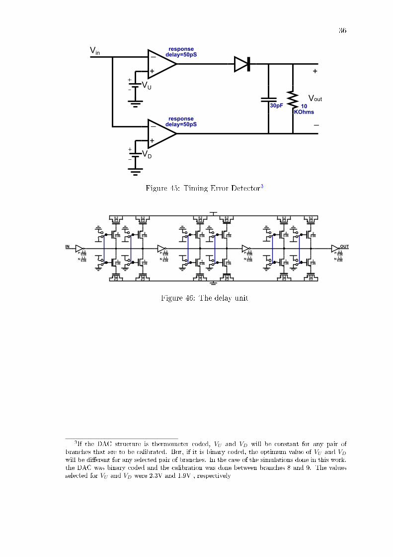
36
VU
VD
Vin
+
_
Vout
+
+
_
_responsedelay=50pS
responsedelay=50pS
30pF 10KOhms
Figure 45: Timing Error Detector3
OUTIN
1
0.06
0.2
0.2
0.2
0.2
0.2
0.2
0.2
0.2
0.2
0.2
0.2
0.2
1
0.06
1
0.06
1
0.06
1
0.06
1
0.06
P:2.2
0.06
N:1.1
0.06
P:2.2
0.06
N:1.1
0.06
0.2
0.2
0.2
0.2
0.2
0.2
0.2
0.2
0.2
0.2
0.2
0.2
2
0.06
2
0.06
2
0.06
2
0.06
2
0.06
2
0.06
P:2.2
0.06
N:1.1
0.06
P:2.2
0.06
N:1.1
0.06
Figure 46: The delay unit
3If the DAC structure is thermometer coded, VU and VD will be constant for any pair ofbranches that are to be calibrated. But, if it is binary coded, the optimum value of VU and VD
will be dierent for any selected pair of branches. In the case of the simulations done in this work,the DAC was binary coded and the calibration was done between branches 8 and 9. The valuesselected for VU and VD were 2.3V and 1.9V , respectively

37
4.2 Calibration process and simulation results
For calibrating the DAC, a calibration process should be performed at start up ofthe IC. Then the position of the switches of the delay units of all branches will besaved in a memory and will be applied to the switches during normal work of theDAC.4 The calibration process is as follows:
One branch will be selected as the reference branch. Half of the capacitor pairsof the delay unit of this branch will be included in the circuit and half of them willbe disconnected. In the case of this design it means 3 pairs of capacitors. Now, otherbranches should be calibrated with respect to this branch one by one. So, we chooseone of the other branches and after calibrating that we continue with the remainingbranches in the same way. We disconnect all the capacitors of the delay unit of thebranch that we are going to calibrate. Then we apply two synchronized pulses tothis branch and the reference branch (The input to other branches are zero). Now,we measure the DC voltage at the output of the timing error detector circuit andrecord it. Then we involve one pair of the capacitors of the delay unit of the branchthat is under calibration and record the DC voltage at the output of the timing errordetector unit again. We continue like this until all six pairs of capacitors of the delayunit of the branch that is to be calibrated are connected. Now, by comparing therecorded DC voltages, we choose the state as the best calibrated state that hasresulted in minimum DC voltage. We do the same procedure for the rest of thebranches.
We designed the circuit of Figure 41 in eldo, in 65nm CMOS technology. TheDAC was intended to work with 2GHz, binary coded input. In order to show theperformance of the design, we inserted a delay of 8pS in branch 9, as depicted inthe gure below:
FF
FF
CLK
CLK
Vout+ -
Delay
Unit
Delay
Unit
Data
Delay
8pS
delay
8pS
delay
2.5V 2.5V
Figure 47: Unit cell of branch 9 with 8pS inserted delay
Then by choosing branch 8 as the reference branch, we tried to calibrate branch9 with respect to it. So, we connected 3 of 6 capacitor pairs of the delay unit of
4Obviously, in this simulation we have not designed the memory and the task for this part isdone manually

38
branch 8. In this simulation for the case of simplicity, we didn't insert timing errorto branches 1 to 8. So, they are already all calibrated with respect to each other.So, in order to not ruin their calibration, we connected 3 of 6 capacitor pairs of eachof the delay units of branches 1 to 7 as well.
By referring to Table 4 we can see that delay units of branches 1 to 8 add a delayof approximately 71pS to the signal ow. For compensating the 8pS delay that isinserted in branch 9, the delay that the delay unit of this branch adds, should be8pS less than other branches, i.e., 63pS. In Table 4 we can see that for the caseof having one capacitor pair connected, the delay created by the delay unit will beapproximately 63pS. So, we expect the calibration process to return minimum DCvoltage for the case of one capacitor pair connected. The calibration process wasdone. Its results are tabulated below:
Pairs of capacitors connected inthe delay unit of branch 9
The DC voltage at the output ofthe error detector
0 139 mV1 129 mV2 145 mV3 146 mV4 144 mV5 165 mV6 162 mV
Table 5: Calibration process results
As it was expected, we can see that we have got the minimum DC voltage forthe case of having one capacitor pair connected.
In order to show the performance of the circuit, we gave two signals as input tothe DAC and measured the output before and after calibration.
One of the inputs was a 26MHz sinusoid with a digital data rate of 2GHz (2 GSamples/Second). In Figure 48 you can nd the output of the DAC to this signalin time domain, before and after calibration. We can see how the calibration hasdecreased the amplitude of the glitches caused by timing error in branch 9. InFigure 49 the output of the DAC to this signal in frequency domain, before andafter calibration, is illustrated. We can see how the noise oor has decreased aftercalibration.
The other input was a 20MHz wide-band signal at the carrier frequency of 2GHz.The output of the DAC for this case, both before and after calibration, is illustratedin gures 50 and 51. The rst one is in time domain and the second one, in frequencydomain. In time domain, we have zoomed in a short range of time in order to givea clearer view of the glitches. You can see that in the frequency response gure,the amplitude of the signal at the rst harmonic and the second biggest component(excluding harmonics) is illustrated. So, the SFDR before and after calibration is64.39dB and 67.55dB , respectively. So, we can see that calibration has resulted in3.16dB increase in SFDR.
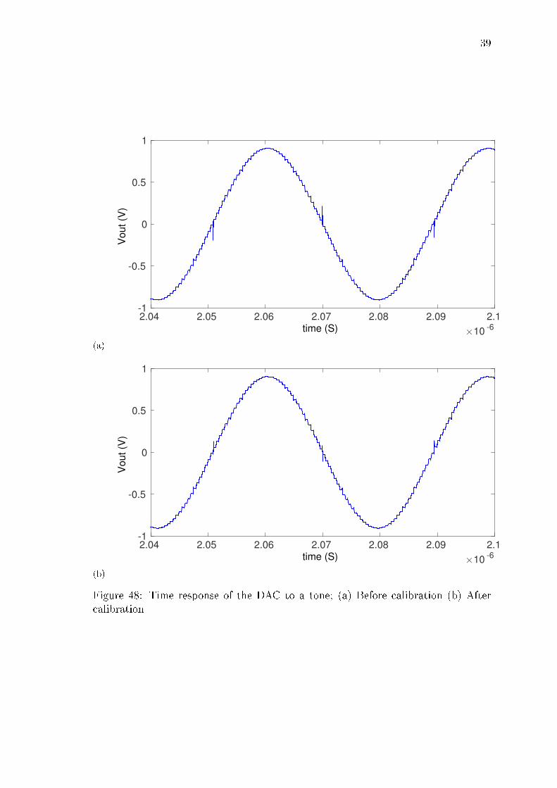
39
(a)
time (S)×10
-6
2.04 2.05 2.06 2.07 2.08 2.09 2.1
Vout (V
)
-1
-0.5
0
0.5
1
(b)
time (S)×10
-6
2.04 2.05 2.06 2.07 2.08 2.09 2.1
Vout (V
)
-1
-0.5
0
0.5
1
Figure 48: Time response of the DAC to a tone; (a) Before calibration (b) Aftercalibration

40
(a)
freq (MHz)-5000 -4000 -3000 -2000 -1000 0 1000 2000 3000 4000 5000
norm
aliz
ed m
agnitude (
dB
)
-120
-100
-80
-60
-40
-20
0
(b)
freq (MHz)-5000 -4000 -3000 -2000 -1000 0 1000 2000 3000 4000 5000
norm
aliz
ed m
agnitude (
dB
)
-120
-100
-80
-60
-40
-20
0
Figure 49: Frequency response of the DAC to a tone; (a) Before calibration (b) Aftercalibration

41
(a)
time (S)×10
-5
1.65 1.66 1.67 1.68 1.69 1.7
Vout (V
)
-0.6
-0.4
-0.2
0
0.2
0.4
(b)
time (S)×10
-5
1.65 1.66 1.67 1.68 1.69 1.7
Vout (V
)
-0.6
-0.4
-0.2
0
0.2
0.4
Figure 50: Time response of the DAC to the wide-band signal; (a) Before calibration(b) After calibration

42
(a)
freq (MHz)-5000 -4000 -3000 -2000 -1000 0 1000 2000 3000 4000 5000
norm
aliz
ed m
agnitude (
dB
)
-120
-100
-80
-60
-40
-20
0 X: 4.703Y: 0
X: 1007Y: -64.39
(b)
freq (MHz)-5000 -4000 -3000 -2000 -1000 0 1000 2000 3000 4000 5000
norm
aliz
ed m
agnitude (
dB
)
-120
-100
-80
-60
-40
-20
0 X: 4.703Y: 0
X: 254.6Y: -67.55
Figure 51: Frequency response of the DAC to the wide-band signal; (a) Beforecalibration (b) After calibration
43
5 Conclusions
The question of this thesis was nding a solution for the problem of glitches thatappear at the output of the DACs that work at high frequencies, due to the timingerror among dierent branches. A solution for this problem was introduced in thisthesis. This approach can be briey explained as follows:
We insert congurable delay blocks in all branches. The delay these blocksgenerate can be changed by a digital control voltage. Through a calibration processwe give specic pulses to the branches and measure their timing error with respectto each other. This timing error measurement is done through a block called timingerror detector. The circuit designed for timing error detector unit has a properresolution and accuracy and is designed in a way that its performance is not aectedby the timing error it might generate itself. Then by changing the control voltageto the delay blocks of the branches we try to minimize their timing error.
A 10 bit binary coded DAC was designed in 65nm technology in eldo simulator.We created a timing error of 8pS in the MSB branches and calibrated it throughthe approach explained above. We tried to check the eciency of this approachby giving a a 26MHz tone and a 20MHz wide-band signal to the DAC, before andafter calibration. The carrier frequency of both signals was 2GHz. In both cases theamplitude of the glitches in time domain had decreased signicantly after calibration.There was a notable decrease in the noise oor of the output for the tone aftercalibration and the SFDR of the output for the wide-band signal was increased byabout 3.2dB after calibration.

44
6 Appendix A- Dynamic ip-ops
The circuit diagram of the ip-op used in this DAC is illustrated in Figure 52.
CLK
CLK
CLK
CLK
D
OUT
D M1
M2
M3
M4
M5
M6
M7
M8
M9
M10
M11
Figure 52: The circuitry of the ip-op used in this thesis
It is a True Single Phase Clock (TSCP) ip-op; meaning that it doesn't need theinvert of clock for its operation [24]. It assures us from not suering any problemscaused by the timing delay between CLK and CLK'. We can see that this ip-op,in contrast with classic ip-ops, has no feedback. So, the question that might ariseis "how does it memorize the previous state?". It memorizes the previous stateby storing it in the parasitic capacitors of the circuit. These kinds of ip-ops arecalled dynamic ip-ops. The advantage of them over ip-ops with feedback istheir higher speed. But, these ip-ops do not work correctly at very low clockfrequencies. It is because their parasitic capacitors will lose their charge [25]. In thefollowing we have analyzed how this ip op works.
An appropriate way for analyzing dynamic ip-ops is to rst analyze the ip-op in dierent stable states and then investigate what happens during transitionsfrom one state to another one. In the case of this ip-op, considering the values ofData and Clock inputs, we will have four dierent states. They are illustrated andanalyzed in gures 53 to 56.

45
CLK
CLK
CLK
CLK
D
OUT
D M1
M2
M3
M4
M5
M6
M7
M8
M9
M10
M11
NETA
NETB NETC
0
0
0
0
0
0
1
~ ~
~
Figure 53: Data=0, CLK=0
CLK
CLK
CLK
CLK
D
OUT
D M1
M2
M3
M4
M5
M6
M7
M8
M9
M10
M11
NETA
NETB NETC
0
1
0
1
1
1
1
0 ~
~
Figure 54: Data=0, CLK=1
CLK
CLK
CLK
CLK
D
OUT
D M1
M2
M3
M4
M5
M6
M7
M8
M9
M10
M11
NETA
NETB NETC
1
0
1
0
0
0
~
~ ~
~
Figure 55: Data=1, CLK=0
CLK
CLK
CLK
CLK
D
OUT
D M1
M2
M3
M4
M5
M6
M7
M8
M9
M10
M11
NETA
NETB NETC
1
1
1
1
1
1
0
0 ~
~
Figure 56: Data=1, CLK=1

46
In these gures the sign ∼ stands for a oating voltage. Nodes specied withthis sign are in a condition that the circuit is not forcing any specic voltage valueto them. So, due to the parasitic capacitors existing at these nodes, they will reservethe voltage value that they had in the previous state of the circuit.
Now, for example, let's consider the case that the input goes from 0 to 1 whilethe clock is 1. This ip-op is a falling edge ip-op. So, for this transition weexpect to see no change at the output. This transition means the change of statefrom Figure 54 to 56. We can see that in Figure 56 the voltages of the output andNETC are oat. So, the voltages of these nodes will be reserved from the previousstate, which means the output will be 0 and NETC will be 1. Now, if a fallingedge on clock signal happens, we expect the output to be updated from 0 to 1. Thistransition means the change of state from Figure 56 to 55. We can see that in Figure55 the voltage of NETA is oat. So, it will inherit the voltage of this node in theprevious state, i.e., 0. This will cause the transistor M5 to conduct and change thevoltage of NETB to 1. Having 1 at NETB, M9 will conduct which will result in thechange of NETC to 0 and consequently, output to 1.

47
7 Appendix B- Comparison between the output of
RF-DAC transmitter and DCT
The drawback of the RF-DAC architecture, compared to DCT is that the outputwill have more high frequency components. So, nice ltering is needed. The reasonis that in RF-DAC we are creating pulses as the carrier signal while in DCT it issinusoid. In gures 57 and 58 the output of a DCT and RF-DAC for the case of onedimensional modulation (i.e., we have just the I signal) is presented.
Figure 57: Amplitude modulated signal by DCT
Figure 58: Amplitude modulated signal by RF-DAC

48
References
[1] Jerry Lemberg An Upconverting Digital to Analog Converter Master thesis atthe department of Micro- and Nanotechnology, Electrical Engineering school,Aalto University
[2] S. Luschas, R. Schreier, and H.-S. Lee Radio frequency digital-to-analog con-verter Solid-State Circuits, IEEE Journal of, vol. 39, no. 9, pp. 1462-1467, sept.2004.
[3] Martin Clara High-Performance D/A-Converters, Application to DigitalTransceivers
[4] Abhishek Yadav Digital Communication
[5] Maxim Integrated Application notes, ID NO. 641
[6] Yongjian Tang, Hans Hegt, Arthur van Roermund Dynamic-Mismatch Mappingfor Digitally-Assisted DACs
[7] Marko Kosunen Digital signal processing and digital-to-analog converters forwide-band transmitters Doctoral dissertation, Helsinki university of technology,Electronic circuit design laboratory- Espoo 2006
[8] Cassius C Cutler Transmission systems employing quantization Patent US2927962 A, 26 April 1954
[9] John WatkinsonArt of Digital Audio Analog Devices, Application note 283
[10] Franco Maloberti Data Converters
[11] George I Bourdopoulos, Aristodemos Pnevmatikakis, Vassilis Anastassopoulos,Theodore L Deliyannis Delta-Sigma Modulators- Modeling, Design, and Appli-cations Imperial College Press
[12] Kyehyung Lee High Eciency Delta-sigma Modulation Data Converters
[13] Kaveh Hosseini, Michael Peter Kennedy Minimizing Spurious Tones in DigitalDelta-Sigma Modulators
[14] Sigma-Delta ADCs and DACs Analog Devices, Application note 283
[15] Behzad Razavi RF Microelectronics, 2nd edition
[16] Alex R. bugeja, member IEEE, and Bang-Sup Song, fellow, IEEE A self-trimming 14-b 100-MS/s CMOS DAC IEEE Journal of solid state circuits,VOL. 35, NO. 12, DECEMBER 2000

49
[17] John Hyde, member, IEEE, Todd Humes, member, IEEE, Chris Diorio, mem-ber, IEEE, Mike Thomas, and Miguel Figueroa A 300-MS/s 14-bit Digital toanalog Converter in Logic CMOS IEEE Journal of solid state circuits, VOL.38, NO. 5, MAY 2003
[18] Yonghua Cong, Randall L. Geiger A 1.5V 14b 100MS/s self-calibrated DACISSCC 2003/Session 7/DACs and AMPs/Paper 7.2
[19] Qiuting Huang1, Pier Andrea Francese1, Chiara Martelli1, Jannik Nielsen A200MS/s 14b 97mW DAC in 0.18Î1
4m CMOS ISSCC 2004 / SESSION 20 /
DIGITAL-TO-ANALOG CONVERTERS / 20.3
[20] K. P. Sunil Rafeeque and Vinita VasudevanA New Technique for On-Chip ErrorEstimation and Reconguration of Current-Steering Digital-to-Analog Convert-ers IEEE TRANSACTIONS ON CIRCUITS AND SYSTEMS-I: REGULARPAPERS, VOL. 52, NO. 11, NOVEMBER 2005
[21] Georgi I. Radulov, Patrick J. Quinn, Hans Hegt, and Arthur van RoermundAn on-chip self-calibration method for current mismatch in D/A ConvertersProceedings of ESSCIRC, Grenoble, France, 2005
[22] Tao Chen, Member, IEEE, and Georges G. E. Gielen, Fellow, IEEE A 14-bit 200-MHz Current-Steering DAC With Switching-Sequence Post-AdjustmentCalibration IEEE JOURNAL OF SOLID-STATE CIRCUITS, VOL. 42, NO.11, NOVEMBER 2007
[23] Yongjian Tang, Joost Briaire, Kostas Doris, Robert van Veldhoven, Pieter C.W. van Beek, Hans Johannes A. Hegt, Senior Member, IEEE, and Arthur H. M.van Roermund, Senior Member, IEEE A 14 bit 200 MS/s DAC With SFDR 78dBc, IM3 < -83 dBc and NSD < -163 dBm/Hz Across the Whole Nyquist BandEnabled by Dynamic-Mismatch Mapping IEEE JOURNAL OF SOLID-STATECIRCUITS, VOL. 46, NO. 6, JUNE 2011
[24] Dr. Paul D. Franzon Latches and Flip-Flops NC state University
[25] Jiren Yuan, Christer Svensson New single-clock CMOS Latches and FlipFlopswith Improved Speed and Power Savings IEEE Journal of Solid State Circuits,VOL. 32, NO. 1, JANUARY 1997