tl494 pulse-width-modulationcontrol circuits · tl494 pulse-width-modulationcontrol circuits...
TRANSCRIPT
www.ti.com
FEATURES
1
2
3
4
5
6
7
8
16
15
14
13
12
11
10
9
1IN+1IN−
FEEDBACKDTC
CTRT
GNDC1
2IN+2IN−REFOUTPUT CTRLVCC
C2E2E1
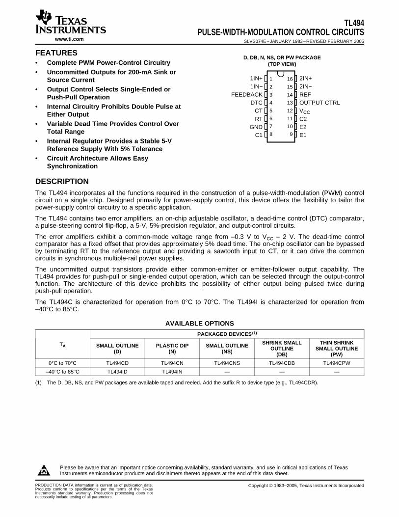
D, DB, N, NS, OR PW PACKAGE(TOP VIEW)
DESCRIPTION
TL494PULSE-WIDTH-MODULATION CONTROL CIRCUITS
SLVS074E–JANUARY 1983–REVISED FEBRUARY 2005
• Complete PWM Power-Control Circuitry• Uncommitted Outputs for 200-mA Sink or
Source Current• Output Control Selects Single-Ended or
Push-Pull Operation• Internal Circuitry Prohibits Double Pulse at
Either Output• Variable Dead Time Provides Control Over
Total Range• Internal Regulator Provides a Stable 5-V
Reference Supply With 5% Tolerance• Circuit Architecture Allows Easy
Synchronization
The TL494 incorporates all the functions required in the construction of a pulse-width-modulation (PWM) controlcircuit on a single chip. Designed primarily for power-supply control, this device offers the flexibility to tailor thepower-supply control circuitry to a specific application.
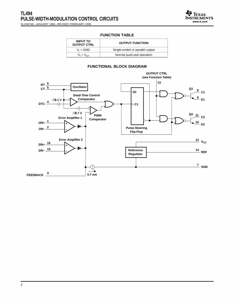
The TL494 contains two error amplifiers, an on-chip adjustable oscillator, a dead-time control (DTC) comparator,a pulse-steering control flip-flop, a 5-V, 5%-precision regulator, and output-control circuits.
The error amplifiers exhibit a common-mode voltage range from –0.3 V to VCC – 2 V. The dead-time controlcomparator has a fixed offset that provides approximately 5% dead time. The on-chip oscillator can be bypassedby terminating RT to the reference output and providing a sawtooth input to CT, or it can drive the commoncircuits in synchronous multiple-rail power supplies.
The uncommitted output transistors provide either common-emitter or emitter-follower output capability. TheTL494 provides for push-pull or single-ended output operation, which can be selected through the output-controlfunction. The architecture of this device prohibits the possibility of either output being pulsed twice duringpush-pull operation.
The TL494C is characterized for operation from 0°C to 70°C. The TL494I is characterized for operation from–40°C to 85°C.
AVAILABLE OPTIONS
PACKAGED DEVICES (1)
SHRINK SMALL THIN SHRINKTA SMALL OUTLINE PLASTIC DIP SMALL OUTLINE OUTLINE SMALL OUTLINE(D) (N) (NS) (DB) (PW)
0°C to 70°C TL494CD TL494CN TL494CNS TL494CDB TL494CPW
–40°C to 85°C TL494ID TL494IN — — —
(1) The D, DB, NS, and PW packages are available taped and reeled. Add the suffix R to device type (e.g., TL494CDR).
Please be aware that an important notice concerning availability, standard warranty, and use in critical applications of TexasInstruments semiconductor products and disclaimers thereto appears at the end of this data sheet.
PRODUCTION DATA information is current as of publication date. Copyright © 1983–2005, Texas Instruments IncorporatedProducts conform to specifications per the terms of the TexasInstruments standard warranty. Production processing does notnecessarily include testing of all parameters.
www.ti.com
GND
VCC
ReferenceRegulator
C1
Pulse-SteeringFlip-Flop
C1
1D
DTC
CTRT
PWMComparator
+
−
Error Amplifier 1
≈ 0.1 V
Dead-Time ControlComparator
Oscillator
OUTPUT CTRL(see Function Table)
0.7 mA
E1
C2
E2
+
−
Error Amplifier 2
1IN+
1IN−
2IN+
2IN−
FEEDBACK
REF
65
4
1
2
16
15
3
13
8
9
11
10
12
14
7
Q1
Q2≈ 0.7 V
TL494PULSE-WIDTH-MODULATION CONTROL CIRCUITSSLVS074E–JANUARY 1983–REVISED FEBRUARY 2005
FUNCTION TABLE
INPUT TO OUTPUT FUNCTIONOUTPUT CTRL
VI = GND Single-ended or parallel output
VI = Vref Normal push-pull operation
FUNCTIONAL BLOCK DIAGRAM
2

www.ti.com
Absolute Maximum Ratings (1)
Recommended Operating Conditions
TL494PULSE-WIDTH-MODULATION CONTROL CIRCUITS
SLVS074E–JANUARY 1983–REVISED FEBRUARY 2005
over operating free-air temperature range (unless otherwise noted)
MIN MAX UNIT
VCC Supply voltage (2) 41 V
VI Amplifier input voltage VCC + 0.3 V
VO Collector output voltage 41 V
IO Collector output current 250 mA
D package 73
DB package 82
θJA Package thermal impedance (3) (4) N package 67 °C/W
NS package 64
PW package 108
Lead temperature 1,6 mm (1/16 inch) from case for 10 seconds 260 °C
Tstg Storage temperature range –65 150 °C
(1) Stresses beyond those listed under "absolute maximum ratings" may cause permanent damage to the device. These are stress ratingsonly, and functional operation of the device at these or any other conditions beyond those indicated under "recommended operatingconditions" is not implied. Exposure to absolute-maximum-rated conditions for extended periods may affect device reliability.
(2) All voltages are with respect to the network ground terminal.(3) Maximum power disipation is a function of TJ(max), θJA, and TA. The maximum allowable power dissipation at any allowable ambient
temperatire is PD = (TJ(max) – TA)/θJA. Operating at the absolute maximum TJ of 150°C can affect reliability.(4) The package thermal impedance is calculated in accordance with JESD 51-7.
MIN MAX UNIT
VCC Supply voltage 7 40 V
VI Amplifier input voltage –0.3 VCC – 2 V
VO Collector output voltage 40 V
Collector output current (each transistor) 200 mA
Current into feedback terminal 0.3 mA
fOSC Oscillator frequency 1 300 kHz
CT Timing capacitor 0.47 10000 nF
RT Timing resistor 1.8 500 kΩ
TL494C 0 70TA Operating free-air temperature °C
TL494I –40 85
3

www.ti.com
N
n1
(xn X)2
N 1
Electrical Characteristics
Reference Section
Oscillator Section
Error-Amplifier Section
TL494PULSE-WIDTH-MODULATION CONTROL CIRCUITSSLVS074E–JANUARY 1983–REVISED FEBRUARY 2005
over recommended operating free-air temperature range, VCC = 15 V, f = 10 kHz (unless otherwise noted)
TL494C, TL494IPARAMETER TEST CONDITIONS (1) UNIT
MIN TYP (2) MAX
Output voltage (REF) IO = 1 mA 4.75 5 5.25 V
Input regulation VCC = 7 V to 40 V 2 25 mV
Output regulation IO = 1 mA to 10 mA 1 15 mV
Output voltage change with temperature ∆TA = MIN to MAX 2 10 mV/V
Short-circuit output current (3) REF = 0 V 25 mA
(1) For conditions shown as MIN or MAX, use the appropriate value specified under recommended operating conditions.(2) All typical values, except for parameter changes with temperature, are at TA = 25°C.(3) Duration of short circuit should not exceed one second.
CT = 0.01 µF, RT = 12 kΩ (see Figure 1)
TL494C, TL494IPARAMETER TEST CONDITIONS (1) UNIT
MIN TYP (2) MAX
Frequency 10 kHz
Standard deviation of frequency (3) All values of VCC, CT, RT, and TA constant 100 Hz/kHz
Frequency change with voltage VCC = 7 V to 40 V, TA = 25°C 1 Hz/kHz
Frequency change with temperature (4) ∆TA = MIN to MAX 10 Hz/kHz
(1) For conditions shown as MIN or MAX, use the appropriate value specified under recommended operating conditions.(2) All typical values, except for parameter changes with temperature, are at TA = 25°C.(3) Standard deviation is a measure of the statistical distribution about the mean as derived from the formula:
(4) Temperature coefficient of timing capacitor and timing resistor are not taken into account.
See Figure 2
TL494C, TL494IPARAMETER TEST CONDITIONS UNIT
MIN TYP (1) MAX
Input offset voltage VO (FEEDBACK) = 2.5 V 2 10 mV
Input offset current VO (FEEDBACK) = 2.5 V 25 250 nA
Input bias current VO (FEEDBACK) = 2.5 V 0.2 1 µA
–0.3 toCommon-mode input voltage range VCC = 7 V to 40 V VVCC – 2
Open-loop voltage amplification ∆VO = 3 V, VO = 0.5 V to 3.5 V, RL = 2 kΩ 70 95 dB
Unity-gain bandwidth VO = 0.5 V to 3.5 V, RL = 2 kΩ 800 kHz
Common-mode rejection ratio ∆VO = 40 V, TA = 25°C 65 80 dB
Output sink current (FEEDBACK) VID = –15 mV to –5 V, V (FEEDBACK) = 0.7 V 0.3 0.7 mA
Output source current (FEEDBACK) VID = 15 mV to 5 V, V (FEEDBACK) = 3.5 V –2 mA
(1) All typical values, except for parameter changes with temperature, are at TA = 25°C.
4

www.ti.com
Electrical Characteristics
Output Section
Dead-Time Control Section
PWM Comparator Section
Total Device
Switching Characteristics
TL494PULSE-WIDTH-MODULATION CONTROL CIRCUITS
SLVS074E–JANUARY 1983–REVISED FEBRUARY 2005
over recommended operating free-air temperature range, VCC = 15 V, f = 10 kHz (unless otherwise noted)
PARAMETER TEST CONDITIONS MIN TYP (1) MAX UNIT
Collector off-state current VCE = 40 V, VCC = 40 V 2 100 µA
Emitter off-state current VCC = VC = 40 V, VE = 0 –100 µA
Common emitter VE = 0, IC = 200 mA 1.1 1.3Collector-emitter saturation voltage V
Emitter follower VO(C1 or C2) = 15 V, IE = –200 mA 1.5 2.5
Output control input current VI = Vref 3.5 mA
(1) All typical values, except for temperature coefficient, are at TA = 25°C.
See Figure 1
PARAMETER TEST CONDITIONS MIN TYP (1) MAX UNIT
Input bias current (DEAD-TIME CTRL) VI = 0 to 5.25 V –2 –10 µA
VI (DEAD-TIME CTRL) = 0, CT = 0.01 µF,Maximum duty cycle, each output 45 %RT = 12 kΩ
Zero duty cycle 3 3.3Input threshold voltage (DEAD-TIME CTRL) V
Maximum duty cycle 0
(1) All typical values, except for temperature coefficient, are at TA = 25°C.
See Figure 1
PARAMETER TEST CONDITIONS MIN TYP (1) MAX UNIT
Input threshold voltage (FEEDBACK) Zero duty cyle 4 4.5 V
Input sink current (FEEDBACK) V (FEEDBACK) = 0.7 V 0.3 0.7 mA
(1) All typical values, except for temperature coefficient, are at TA = 25°C.
PARAMETER TEST CONDITIONS MIN TYP (1) MAX UNIT
VCC = 15 V 6 10RT = Vref,Standby supply current mAAll other inputs and outputs open VCC = 40 V 9 15
Average supply current VI (DEAD-TIME CTRL) = 2 V, See Figure 1 7.5 mA
(1) All typical values, except for temperature coefficient, are at TA = 25°C.
TA = 25°C
PARAMETER TEST CONDITIONS MIN TYP (1) MAX UNIT
Rise time 100 200 nsCommon-emitter configuration, See Figure 3
Fall time 25 100 ns
Rise time 100 200 nsEmitter-follower configuration, See Figure 4
Fall time 40 100 ns
(1) All typical values, except for temperature coefficient, are at TA = 25°C.
5

www.ti.com
PARAMETER MEASUREMENT INFORMATION
TestInputs
DTC
FEEDBACK
RT
CT
GND50 kΩ
12 kΩ
0.01 µF
VCC
REFOUTPUTCTRL
E2
C2
E1
C1 Output 1
Output 2
150 Ω2 W
150 Ω2 W
VCC = 15 V
TEST CIRCUIT
1IN+
VCC
VCC
0 V
0 V
Voltageat C1
Voltageat C2
Voltageat CT
DTC
FEEDBACK
0 V
0.7 V
0% MAX 0%
Threshold Voltage
Threshold Voltage
VOLTAGE WAVEFORMS
Duty Cycle
ErrorAmplifiers
7
14
12
8
9
11
10
4
3
6
5
1
2
16
15
13
1IN−
2IN−
2IN+
TL494PULSE-WIDTH-MODULATION CONTROL CIRCUITSSLVS074E–JANUARY 1983–REVISED FEBRUARY 2005
Figure 1. Operational Test Circuit and Waveforms
6

www.ti.com
PARAMETER MEASUREMENT INFORMATION
+
−
+
−
VI
Vref
FEEDBACK
Amplifier Under Test
Other Amplifier
Output
Each OutputCircuit
68 Ω2 W
15 V
CL = 15 pF(See Note A)
90%
10%
90%
10%
tf tr
TEST CIRCUIT OUTPUT VOLTAGE WAVEFORM
NOTE A: CL includes probe and jig capacitance.
Output
Each OutputCircuit
68 Ω2 W
15 V
CL = 15 pF(See Note A)
90%
10%
90%
10%
tftr
TEST CIRCUIT OUTPUT VOLTAGE WAVEFORM
NOTE A: CL includes probe and jig capacitance.
TL494PULSE-WIDTH-MODULATION CONTROL CIRCUITS
SLVS074E–JANUARY 1983–REVISED FEBRUARY 2005
Figure 2. Amplifier Characteristics
Figure 3. Common-Emitter Configuration
Figure 4. Emitter-Follower Configuration
7

www.ti.com
TYPICAL CHARACTERISTICS
Df = 1%†
40
10
100
1 k 4 k 10 k 40 k 100 k 400 k 1 Mf − O
scill
ato
r F
req
uen
cy a
nd
Fre
qu
ency
Var
iatio
n −
Hz
OSCILLATOR FREQUENCY ANDFREQUENCY VARIATION†
vsTIMING RESISTANCE
400
1 k
4 k
10 k
40 k
100 k
RT − Timing Resistance − Ω
0.1 µF
−2%−1%
0% 0.01 µF
0.001 µF
VCC = 15 VTA = 25°C
CT = 1 µF
† Frequency variation (∆f) is the change in oscillator frequency that occurs over the full temperature range.
10
0
100
20
1 10 100 1 M
A −
Am
plif
ier
Vo
ltag
e A
mp
lific
atio
n −
dB
30
f − Frequency − Hz
AMPLIFIER VOLTAGE AMPLIFICATIONvs
FREQUENCY
1 k
VCC = 15 V∆VO = 3 VTA = 25°C
10 k
40
50
60
70
80
90
100 k
TL494PULSE-WIDTH-MODULATION CONTROL CIRCUITSSLVS074E–JANUARY 1983–REVISED FEBRUARY 2005
Figure 5.
Figure 6.
8
PACKAGING INFORMATION
Orderable Device Status (1) PackageType
PackageDrawing
Pins PackageQty
Eco Plan (2) Lead/Ball Finish MSL Peak Temp (3)
TL494CD ACTIVE SOIC D 16 40 Green (RoHS &no Sb/Br)
CU NIPDAU Level-1-260C-UNLIM
TL494CDBR ACTIVE SSOP DB 16 2000 Green (RoHS &no Sb/Br)
CU NIPDAU Level-1-260C-UNLIM
TL494CDBRE4 ACTIVE SSOP DB 16 2000 Green (RoHS &no Sb/Br)
CU NIPDAU Level-1-260C-UNLIM
TL494CDBRG4 ACTIVE SSOP DB 16 2000 Green (RoHS &no Sb/Br)
CU NIPDAU Level-1-260C-UNLIM
TL494CDE4 ACTIVE SOIC D 16 40 Green (RoHS &no Sb/Br)
CU NIPDAU Level-1-260C-UNLIM
TL494CDG4 ACTIVE SOIC D 16 40 Green (RoHS &no Sb/Br)
CU NIPDAU Level-1-260C-UNLIM
TL494CDR ACTIVE SOIC D 16 2500 Green (RoHS &no Sb/Br)
CU NIPDAU Level-1-260C-UNLIM
TL494CDRE4 ACTIVE SOIC D 16 2500 Green (RoHS &no Sb/Br)
CU NIPDAU Level-1-260C-UNLIM
TL494CDRG4 ACTIVE SOIC D 16 2500 Green (RoHS &no Sb/Br)
CU NIPDAU Level-1-260C-UNLIM
TL494CJ OBSOLETE CDIP J 16 TBD Call TI Call TI
TL494CN ACTIVE PDIP N 16 25 Pb-Free(RoHS)
CU NIPDAU N / A for Pkg Type
TL494CNE4 ACTIVE PDIP N 16 25 Pb-Free(RoHS)
CU NIPDAU N / A for Pkg Type
TL494CNSR ACTIVE SO NS 16 2000 Green (RoHS &no Sb/Br)
CU NIPDAU Level-1-260C-UNLIM
TL494CNSRG4 ACTIVE SO NS 16 2000 Green (RoHS &no Sb/Br)
CU NIPDAU Level-1-260C-UNLIM
TL494CPW ACTIVE TSSOP PW 16 90 Green (RoHS &no Sb/Br)
CU NIPDAU Level-1-260C-UNLIM
TL494CPWE4 ACTIVE TSSOP PW 16 90 Green (RoHS &no Sb/Br)
CU NIPDAU Level-1-260C-UNLIM
TL494CPWG4 ACTIVE TSSOP PW 16 90 Green (RoHS &no Sb/Br)
CU NIPDAU Level-1-260C-UNLIM
TL494CPWLE OBSOLETE TSSOP PW 16 TBD Call TI Call TI
TL494CPWR ACTIVE TSSOP PW 16 2000 Green (RoHS &no Sb/Br)
CU NIPDAU Level-1-260C-UNLIM
TL494CPWRE4 ACTIVE TSSOP PW 16 2000 Green (RoHS &no Sb/Br)
CU NIPDAU Level-1-260C-UNLIM
TL494CPWRG4 ACTIVE TSSOP PW 16 2000 Green (RoHS &no Sb/Br)
CU NIPDAU Level-1-260C-UNLIM
TL494ID ACTIVE SOIC D 16 40 Green (RoHS &no Sb/Br)
CU NIPDAU Level-1-260C-UNLIM
TL494IDE4 ACTIVE SOIC D 16 40 Green (RoHS &no Sb/Br)
CU NIPDAU Level-1-260C-UNLIM
TL494IDG4 ACTIVE SOIC D 16 40 Green (RoHS &no Sb/Br)
CU NIPDAU Level-1-260C-UNLIM
TL494IDR ACTIVE SOIC D 16 2500 Green (RoHS &no Sb/Br)
CU NIPDAU Level-1-260C-UNLIM
TL494IDRE4 ACTIVE SOIC D 16 2500 Green (RoHS & CU NIPDAU Level-1-260C-UNLIM
PACKAGE OPTION ADDENDUM
www.ti.com 28-May-2007
Addendum-Page 1

Orderable Device Status (1) PackageType
PackageDrawing
Pins PackageQty
Eco Plan (2) Lead/Ball Finish MSL Peak Temp (3)
no Sb/Br)
TL494IDRG4 ACTIVE SOIC D 16 2500 Green (RoHS &no Sb/Br)
CU NIPDAU Level-1-260C-UNLIM
TL494IN ACTIVE PDIP N 16 25 Pb-Free(RoHS)
CU NIPDAU N / A for Pkg Type
TL494INE4 ACTIVE PDIP N 16 25 Pb-Free(RoHS)
CU NIPDAU N / A for Pkg Type
TL494MJ OBSOLETE CDIP J 16 TBD Call TI Call TI
TL494MJB OBSOLETE CDIP J 16 TBD Call TI Call TI
(1) The marketing status values are defined as follows:ACTIVE: Product device recommended for new designs.LIFEBUY: TI has announced that the device will be discontinued, and a lifetime-buy period is in effect.NRND: Not recommended for new designs. Device is in production to support existing customers, but TI does not recommend using this part ina new design.PREVIEW: Device has been announced but is not in production. Samples may or may not be available.OBSOLETE: TI has discontinued the production of the device.
(2) Eco Plan - The planned eco-friendly classification: Pb-Free (RoHS), Pb-Free (RoHS Exempt), or Green (RoHS & no Sb/Br) - please checkhttp://www.ti.com/productcontent for the latest availability information and additional product content details.TBD: The Pb-Free/Green conversion plan has not been defined.Pb-Free (RoHS): TI's terms "Lead-Free" or "Pb-Free" mean semiconductor products that are compatible with the current RoHS requirementsfor all 6 substances, including the requirement that lead not exceed 0.1% by weight in homogeneous materials. Where designed to be solderedat high temperatures, TI Pb-Free products are suitable for use in specified lead-free processes.Pb-Free (RoHS Exempt): This component has a RoHS exemption for either 1) lead-based flip-chip solder bumps used between the die andpackage, or 2) lead-based die adhesive used between the die and leadframe. The component is otherwise considered Pb-Free (RoHScompatible) as defined above.Green (RoHS & no Sb/Br): TI defines "Green" to mean Pb-Free (RoHS compatible), and free of Bromine (Br) and Antimony (Sb) based flameretardants (Br or Sb do not exceed 0.1% by weight in homogeneous material)
(3) MSL, Peak Temp. -- The Moisture Sensitivity Level rating according to the JEDEC industry standard classifications, and peak soldertemperature.
Important Information and Disclaimer:The information provided on this page represents TI's knowledge and belief as of the date that it isprovided. TI bases its knowledge and belief on information provided by third parties, and makes no representation or warranty as to theaccuracy of such information. Efforts are underway to better integrate information from third parties. TI has taken and continues to takereasonable steps to provide representative and accurate information but may not have conducted destructive testing or chemical analysis onincoming materials and chemicals. TI and TI suppliers consider certain information to be proprietary, and thus CAS numbers and other limitedinformation may not be available for release.
In no event shall TI's liability arising out of such information exceed the total purchase price of the TI part(s) at issue in this document sold by TIto Customer on an annual basis.
PACKAGE OPTION ADDENDUM
www.ti.com 28-May-2007
Addendum-Page 2

TAPE AND REEL BOX INFORMATION
Device Package Pins Site ReelDiameter
(mm)
ReelWidth(mm)
A0 (mm) B0 (mm) K0 (mm) P1(mm)
W(mm)
Pin1Quadrant
TL494CDBR DB 16 SITE 41 330 16 8.2 6.6 2.5 12 16 Q1
TL494CDR D 16 SITE 27 330 16 6.5 10.3 2.1 8 16 Q1
TL494CDR D 16 SITE 41 330 16 6.5 10.3 2.1 8 16 Q1
TL494CNSR NS 16 SITE 41 330 16 8.2 10.5 2.5 12 16 Q1
TL494CPWR PW 16 SITE 41 330 12 7.0 5.6 1.6 8 12 Q1
TL494IDR D 16 SITE 27 330 16 6.5 10.3 2.1 8 16 Q1
PACKAGE MATERIALS INFORMATION
www.ti.com 12-Jan-2008
Pack Materials-Page 1
Device Package Pins Site Length (mm) Width (mm) Height (mm)
TL494CDBR DB 16 SITE 41 346.0 346.0 33.0
TL494CDR D 16 SITE 27 342.9 345.9 28.58
TL494CDR D 16 SITE 41 346.0 346.0 33.0
TL494CNSR NS 16 SITE 41 346.0 346.0 33.0
TL494CPWR PW 16 SITE 41 346.0 346.0 29.0
TL494IDR D 16 SITE 27 342.9 345.9 28.58
PACKAGE MATERIALS INFORMATION
www.ti.com 12-Jan-2008
Pack Materials-Page 2

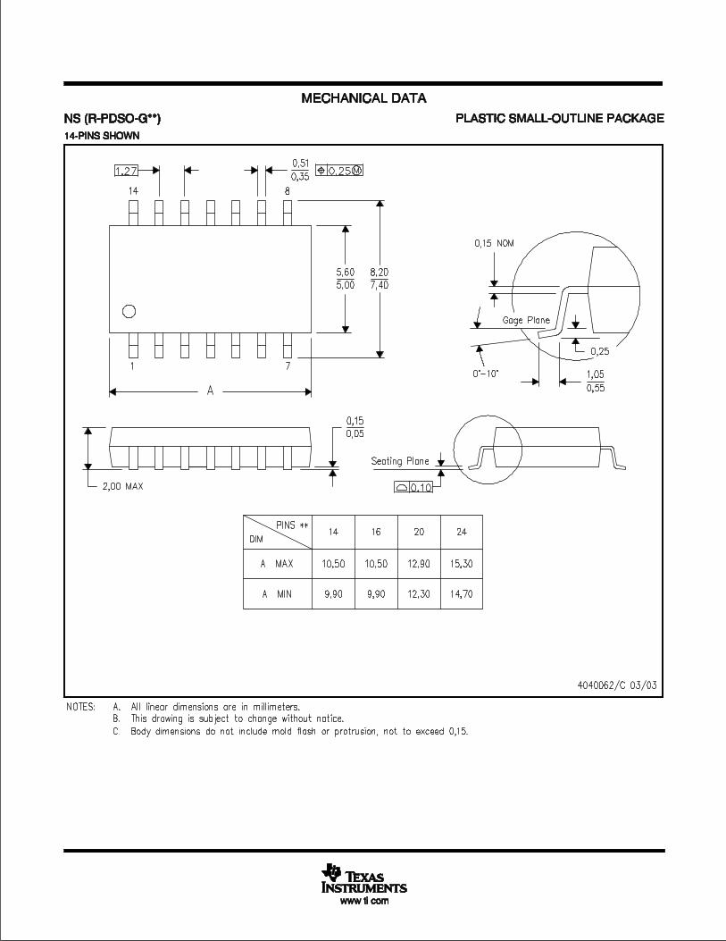

MECHANICAL DATA
MTSS001C – JANUARY 1995 – REVISED FEBRUARY 1999
POST OFFICE BOX 655303 • DALLAS, TEXAS 75265
PW (R-PDSO-G**) PLASTIC SMALL-OUTLINE PACKAGE14 PINS SHOWN
0,65 M0,10
0,10
0,25
0,500,75
0,15 NOM
Gage Plane
28
9,80
9,60
24
7,90
7,70
2016
6,60
6,40
4040064/F 01/97
0,30
6,606,20
8
0,19
4,304,50
7
0,15
14
A
1
1,20 MAX
14
5,10
4,90
8
3,10
2,90
A MAX
A MIN
DIMPINS **
0,05
4,90
5,10
Seating Plane
0°–8°
NOTES: A. All linear dimensions are in millimeters.B. This drawing is subject to change without notice.C. Body dimensions do not include mold flash or protrusion not to exceed 0,15.D. Falls within JEDEC MO-153

1 www.handsontec.com
Handsontec.com
HandsOn Technology provides a multimedia and interactive platform for
everyone interested in electronics. From beginner to diehard, from student to
lecturer. Information, education, inspiration and entertainment. Analog and
digital, practical and theoretical; software and hardware.
HandsOn Technology support Open Source Hardware (OSHW) Development Platform.
Learn : Design : Share
www.handsontec.com

2 www.handsontec.com
The Face behind our product quality…
In a world of constant change and continuous technological development, a new or replacement product
is never far away – and they all need to be tested.
Many vendors simply import and sell wihtout checks and this cannot be the ultimate interests of anyone,
particularly the customer. Every part sell on Handsotec is fully tested. So when buying from Handsontec
products range, you can be confident you’re getting outstanding quality and value.
We keep adding the new parts so that you can get rolling on your next project.
Breakout Boards & Modules
Connectors Electro-Mechanical Parts
Engineering Material
Mechanical Hardware
P
Electronics Components
Power Supply Arduino Board & Shield
Tools & Accessory