tlc374, tlc374q, tlc374y lincmos quadruple … · fk package (top view) 2out 1out nc 3in+ ... (y)...
TRANSCRIPT
1
2
3
4
5
6
7
14
13
12
11
10
9
8
1OUT2OUT
VDD2IN–2IN+1IN–1IN+
3OUT4OUTGND4IN+4IN–3IN+3IN–
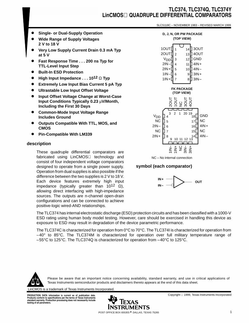
D, J, N, OR PW PACKAGE(TOP VIEW)
3 2 1 20 19
9 10 11 12 13
4
5
6
7
8
18
17
16
15
14
GNDNC4IN+NC4IN–
VDDNC
2IN–NC
2IN+
FK PACKAGE(TOP VIEW)
2OU
T1O
UT
NC
3IN
+4O
UT
1IN
–1I
N+
NC
NC – No internal connection
3IN
–3O
UT
symbol (each comparator)
IN+
IN–OUT
TLC374, TLC374Q, TLC374YLinCMOS QUADRUPLE DIFFERENTIAL COMPARATORS
SLCS118C – NOVEMBER 1983 – REVISED MARCH 1999
1POST OFFICE BOX 655303 • DALLAS, TEXAS 75265
Single- or Dual-Supply Operation
Wide Range of Supply Voltages2 V to 18 V
Very Low Supply Current Drain 0.3 mA Typat 5 V
Fast Response Time . . . 200 ns Typ forTTL-Level Input Step
Built-In ESD Protection
High Input Impedance . . . 1012 Ω Typ
Extremely Low Input Bias Current 5 pA Typ
Ultrastable Low Input Offset Voltage
Input Offset Voltage Change at Worst-CaseInput Conditions Typically 0.23 µV/Month,Including the First 30 Days
Common-Mode Input Voltage RangeIncludes Ground
Outputs Compatible With TTL, MOS, andCMOS
Pin-Compatible With LM339
description
These quadruple differential comparators arefabricated using LinCMOS technology andconsist of four independent voltage comparatorsdesigned to operate from a single power supply.Operation from dual supplies is also possible if thedifference between the two supplies is 2 V to 18 V.Each device features extremely high inputimpedance (typically greater than 1012 Ω),allowing direct interfacing with high-impedancesources. The outputs are n-channel open-drainconfigurations and can be connected to achievepositive-logic wired-AND relationships.
The TLC374 has internal electrostatic discharge (ESD) protection circuits and has been classified with a 1000-VESD rating using human body model testing. However, care should be exercised in handling this device asexposure to ESD may result in degradation of the device parametric performance.
The TLC374C is characterized for operation from 0°C to 70°C. The TLC374I is characterized for operation from–40° to 85°C. The TLC374M is characterized for operation over full military temperature range of–55°C to 125°C. The TLC374Q is characterized for operation from –40°C to 125°C.
Please be aware that an important notice concerning availability, standard warranty, and use in critical applications ofTexas Instruments semiconductor products and disclaimers thereto appears at the end of this data sheet.
Copyright 1999, Texas Instruments IncorporatedPRODUCTION DATA information is current as of publication date.Products conform to specifications per the terms of Texas Instrumentsstandard warranty. Production processing does not necessarily includetesting of all parameters.
LinCMOS is a trademark of Texas Instruments Incorporated.
TLC374, TLC374Q, TLC374YLinCMOS QUADRUPLE DIFFERENTIAL COMPARATORS
SLCS118C – NOVEMBER 1983 – REVISED MARCH 1999
2 POST OFFICE BOX 655303 • DALLAS, TEXAS 75265
AVAILABLE OPTIONS
VIO maxPACKAGED DEVICES CHIP
TAVIO maxAT 25°C SMALL OUTLINE
(D)CHIP CARRIER
(FK)CERAMIC DIP
(J)PLASTIC DIP
(N)TSSOP(PW)
FORM(Y)
0°C to 70°C 5 mV TLC374CD — — TLC374CN TLC374CPW TLC374Y
–40°C to 85°C 5 mV TLC374ID — — TLC374IN — —
–55°C to 125°C 5 mV TLC374MD TLC374MFK TLC374MJ TLC374MN — —
–40°C to 125°C 5 mV TLC374QD — — TLC374QN — —
The D packages are available taped and reeled. Add R suffix to device type (e.g., TLC374CDR).
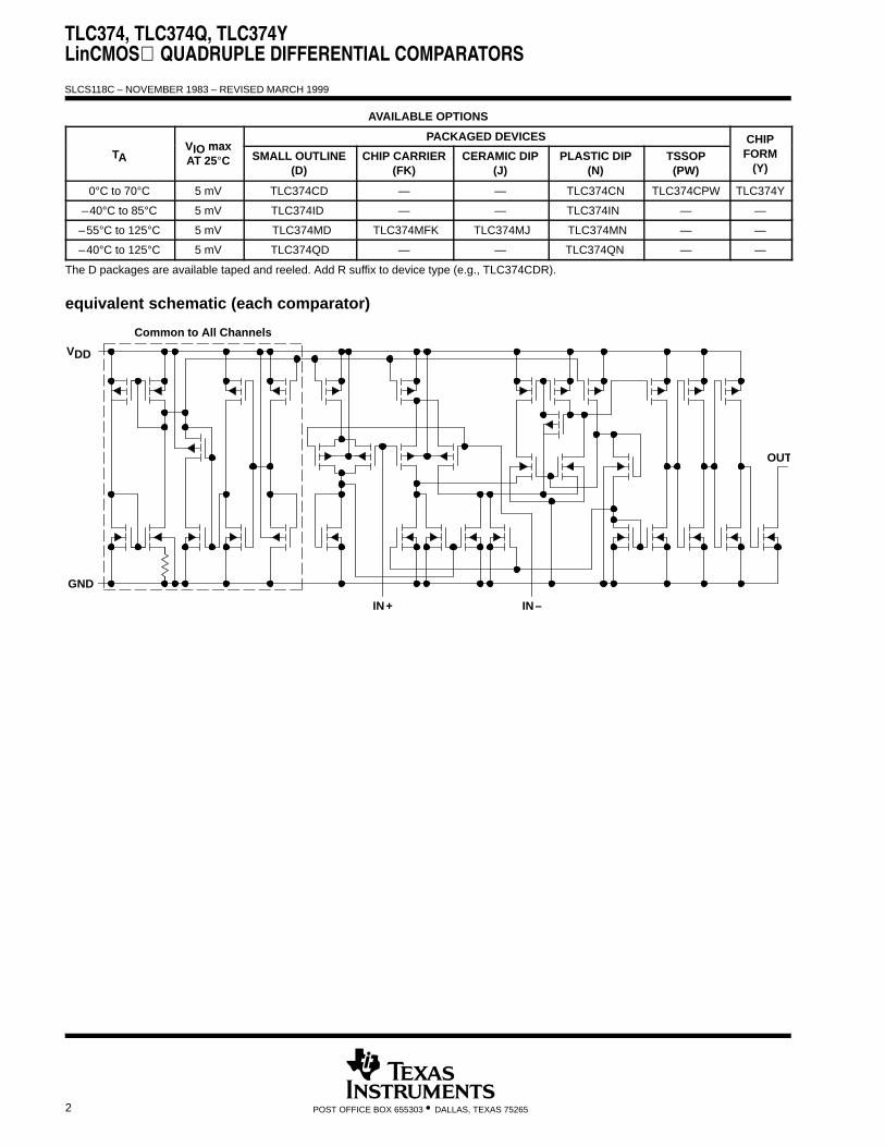
equivalent schematic (each comparator)
VDD
GND
IN+ IN–
OUT
Common to All Channels
TLC374, TLC374Q, TLC374YLinCMOS QUADRUPLE DIFFERENTIAL COMPARATORS
SLCS118C – NOVEMBER 1983 – REVISED MARCH 1999
3POST OFFICE BOX 655303 • DALLAS, TEXAS 75265
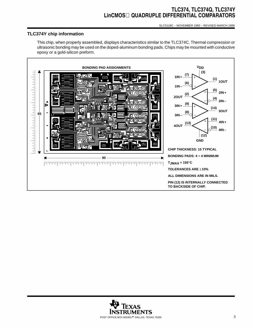
TLC374Y chip information
This chip, when properly assembled, displays characteristics similar to the TLC374C. Thermal compression orultrasonic bonding may be used on the doped-aluminum bonding pads. Chips may be mounted with conductiveepoxy or a gold-silicon preform.
BONDING PAD ASSIGNMENTS
CHIP THICKNESS: 15 TYPICAL
BONDING PADS: 4 × 4 MINIMUM
TJMAX = 150°C
TOLERANCES ARE ±10%
ALL DIMENSIONS ARE IN MILS.
PIN (12) IS INTERNALLY CONNECTEDTO BACKSIDE OF CHIP.
+
–3OUT
3IN+
3IN–
GND
(10)
(9)
(8)
(11)
(14)
–
+(13) 4IN+
4IN–4OUT
(12)
+
–
VDD(3)
(4)
(7)
(6)
(5)
(1)
–
+(2)
65
90
1IN+
1IN–
2OUT
1OUT
2IN+
2IN–
(13)
(14)
(1)
(2) (3) (4) (5) (6)
(7)
(8)
(9)(10)(11)(12)

TLC374, TLC374Q, TLC374YLinCMOS QUADRUPLE DIFFERENTIAL COMPARATORS
SLCS118C – NOVEMBER 1983 – REVISED MARCH 1999
4 POST OFFICE BOX 655303 • DALLAS, TEXAS 75265
absolute maximum ratings over operating free-air temperature range (unless otherwise noted)†
Supply voltage, VDD (see Note 1) 18 V. . . . . . . . . . . . . . . . . . . . . . . . . . . . . . . . . . . . . . . . . . . . . . . . . . . . . . . . . . . . Differential input voltage, VID (see Note 2) ±18 V. . . . . . . . . . . . . . . . . . . . . . . . . . . . . . . . . . . . . . . . . . . . . . . . . . . Input voltage, VI VDD. . . . . . . . . . . . . . . . . . . . . . . . . . . . . . . . . . . . . . . . . . . . . . . . . . . . . . . . . . . . . . . . . . . . . . . . . . . Input voltage range, VI –0.3 V to 18 V. . . . . . . . . . . . . . . . . . . . . . . . . . . . . . . . . . . . . . . . . . . . . . . . . . . . . . . . . . . . . Output voltage, VO 18 V. . . . . . . . . . . . . . . . . . . . . . . . . . . . . . . . . . . . . . . . . . . . . . . . . . . . . . . . . . . . . . . . . . . . . . . . . Input current, II ±5 mA. . . . . . . . . . . . . . . . . . . . . . . . . . . . . . . . . . . . . . . . . . . . . . . . . . . . . . . . . . . . . . . . . . . . . . . . . . Output current, IO 20 mA. . . . . . . . . . . . . . . . . . . . . . . . . . . . . . . . . . . . . . . . . . . . . . . . . . . . . . . . . . . . . . . . . . . . . . . . Duration of output short circuit to ground (see Note 3) unlimited. . . . . . . . . . . . . . . . . . . . . . . . . . . . . . . . . . . . . . Continuous total power dissipation See Dissipation Rating Table. . . . . . . . . . . . . . . . . . . . . . . . . . . . . . . . . . . . . Operating free-air temperature range, TA: TLC374C 0°C to 70°C. . . . . . . . . . . . . . . . . . . . . . . . . . . . . . . . . . . . .
TLC374I –40°C to 85°C. . . . . . . . . . . . . . . . . . . . . . . . . . . . . . . . . . . . TLC374M –55°C to 125°C. . . . . . . . . . . . . . . . . . . . . . . . . . . . . . . . . . TLC374Q –40°C to 125°C. . . . . . . . . . . . . . . . . . . . . . . . . . . . . . . . . .
Storage temperature range, Tstg –65°C to 150°C. . . . . . . . . . . . . . . . . . . . . . . . . . . . . . . . . . . . . . . . . . . . . . . . . . . Case temperature range for 60 seconds: FK package 260°C. . . . . . . . . . . . . . . . . . . . . . . . . . . . . . . . . . . . . . . . Lead temperature 1,6 mm (1/16 inch) from case for 60 seconds: D, N, or PW package 260°C. . . . . . . . . . . . Lead temperature 1,6 mm (1/16 inch) from case for 10 seconds: J package 300°C. . . . . . . . . . . . . . . . . . . . .
† Stresses beyond those listed under “absolute maximum ratings” may cause permanent damage to the device. These are stress ratings only, andfunctional operation of the device at these or any other conditions beyond those indicated under “recommended operating conditions” is notimplied. Exposure to absolute-maximum-rated conditions for extended periods may affect device reliability.
NOTES: 1. All voltage values except differential voltages are with respect to network ground.2. Differential voltages are at IN+ with respect to IN –.3. Short circuits from outputs to VDD can cause excessive heating and eventual device destruction.
DISSIPATION RATING TABLE
PACKAGETA ≤ 25°C DERATING DERATE TA = 70°C TA = 85°C TA = 125°C
PACKAGE APOWER RATING FACTOR ABOVE TA
APOWER RATING
APOWER RATING
APOWER RATING
D 500 mW 7.6 mW/°C 84°C 500 mW 494 mW 190 mW
FK 500 mW 11.0 mW/°C 104°C 500 mW 500 mW 269 mW
J 500 mW 11.0 mW/°C 104°C 500 mW 500 mW 269 mW
N 500 mW 9.2 mW/°C 95°C 500 mW 500 mW 224 mW
PW 700 mW 5.6 mW/°C — 448 mW — —
recommended operating conditions
TLC374C TLC374I TLC374M TLC374QUNIT
MIN MAX MIN MAX MIN MAX MIN MAXUNIT
Supply voltage, VDD 3 16 3 16 4 16 3 16 V
Common mode input voltage VICVDD = 5 V 0 3.5 0 3.5 0 3.5 0 3.5
VCommon-mode input voltage, VICVDD = 10 V 0 8.5 0 8.5 0 8.5 0 8.5
V
Operating free-air temperature, TA 0 70 –40 85 –55 125 –40 125 °C
TLC374, TLC374Q, TLC374Y
SLC
S118C
– NO
VE
MB
ER
1983 – RE
VIS
ED
MA
RC
H 1999
LinCMO
S Q
UADRUPLE DIFFERENTIAL COM
PARATORS
PO
ST
OF
FIC
E B
OX
655303 DA
LLAS
, TE
XA
S 75265
•5
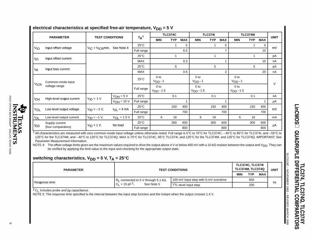
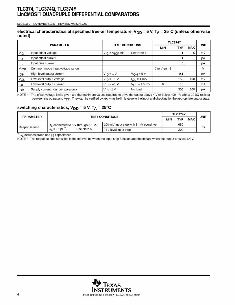
electrical characteristics at specified free-air temperature, VDD = 5 V
PARAMETER TEST CONDITIONS TA†TLC374C TLC374I TLC374M
UNITPARAMETER TEST CONDITIONS TA†MIN TYP MAX MIN TYP MAX MIN TYP MAX
UNIT
VIO Input offset voltage VIC = VICRmin See Note 425°C 1 5 1 5 1 5
mVVIO Input offset voltage VIC = VICRmin, See Note 4Full range 6.5 7 10
mV
IIO Input offset current25°C 1 1 1 pA
IIO Input offset currentMAX 0.3 1 10 nA
IIB Input bias current25°C 5 5 5 pA
IIB Input bias currentMAX 0.6 2 20 nA
VICRCommon-mode input
25°C0 to
VDD–10 to
VDD–10 to
VDD–1VVICR voltage range
Full range0 to
VDD–1.50 to
VDD–1.50 to
VDD–1.5
V
IOH High level output current VID = 1 VVOH = 5 V 25°C 0.1 0.1 0.1 nA
IOH High-level output current VID = 1 VVOH = 15 V Full range 1 1 1 µA
VOL Low level output voltage VID = 1 V IOL = 4 mA25°C 150 400 150 400 150 400
mVVOL Low-level output voltage VID = –1 V, IOL = 4 mAFull range 700 700 700
mV
IOL Low-level output current VID = –1 V, VOL = 1.5 V 25°C 6 16 6 16 6 16 mA
IDDSupply current
VID = 1 V No load25°C 300 600 300 600 300 600
µAIDDy
(four comparators) VID = 1 V, No loadFull range 800 800 800
µA
† All characteristics are measured with zero common-mode input voltage unless otherwise noted. Full range is 0°C to 70°C for TLC374C, –40°C to 85°C for TLC374I, and –55°C to125°C for the TLC374M, and –40°C to 125°C for TLC374Q. MAX is 70°C for TLC374C, 85°C TLC374I, and 125°C for the TLC374M, and 125°C for TLC374Q. IMPORTANT: SeeParameter Measurement Information.
NOTE 4: The offset voltage limits given are the maximum values required to drive the output above 4 V or below 400 mV with a 10-kΩ resistor between the output and VDD. They canbe verified by applying the limit value to the input and checking for the appropriate output state.
switching characteristics, VDD = 5 V, TA = 25°C
PARAMETER TEST CONDITIONS
TLC374C, TLC374ITLC374M, TLC374Q UNITMIN TYP MAX
Response timeRL connected to 5 V through 5.1 kΩ,
‡100-mV input step with 5-mV overdrive 650
nsResponse time L gCL = 15 pF‡, See Note 5 TTL-level input step 200
ns
‡ CL includes probe and jig capacitance.NOTE 5: The response time specified is the interval between the input step function and the instant when the output crosses 1.4 V.
TLC374, TLC374Q, TLC374YLinCMOS QUADRUPLE DIFFERENTIAL COMPARATORS
SLCS118C – NOVEMBER 1983 – REVISED MARCH 1999
6 POST OFFICE BOX 655303 • DALLAS, TEXAS 75265
electrical characteristics at specified free-air temperature, VDD = 5 V, TA = 25°C (unless otherwisenoted)
PARAMETER TEST CONDITIONSTLC374Y
UNITPARAMETER TEST CONDITIONSMIN TYP MAX
UNIT
VIO Input offset voltage VIC = VICRmin, See Note 4 1 5 mV
IIO Input offset current 1 pA
IIB Input bias current 5 pA
VICR Common-mode input voltage range 0 to VDD–1 V
IOH High-level output current VID = 1 V, VOH = 5 V 0.1 nA
VOL Low-level output voltage VID = –1 V, IOL = 4 mA 150 400 mV
IOL Low-level output current VID = –1 V, VOL = 1.5 mV 6 16 mA
IDD Supply current (four comparators) VID =1 V, No load 300 600 µA
NOTE 4: The offset voltage limits given are the maximum values required to drive the output above 4 V or below 400 mV with a 10-kΩ resistorbetween the output and VDD. They can be verified by applying the limit value to the input and checking for the appropriate output state.
switching characteristics, VDD = 5 V, TA = 25°C
PARAMETER TEST CONDITIONSTLC374Y
UNITPARAMETER TEST CONDITIONSMIN TYP MAX
UNIT
Response timeRL connected to 5 V through 5.1 kΩ,
†100-mV input step with 5-mV overdrive 650
nsResponse time L gCL = 15 pF†, See Note 5 TTL-level input step 200
ns
† CL includes probe and jig capacitance.NOTE 4: The response time specified is the interval between the input step function and the instant when the output crosses 1.4 V.
TLC374, TLC374Q, TLC374YLinCMOS QUADRUPLE DIFFERENTIAL COMPARATORS
SLCS118C – NOVEMBER 1983 – REVISED MARCH 1999
7POST OFFICE BOX 655303 • DALLAS, TEXAS 75265
PARAMETER MEASUREMENT INFORMATION
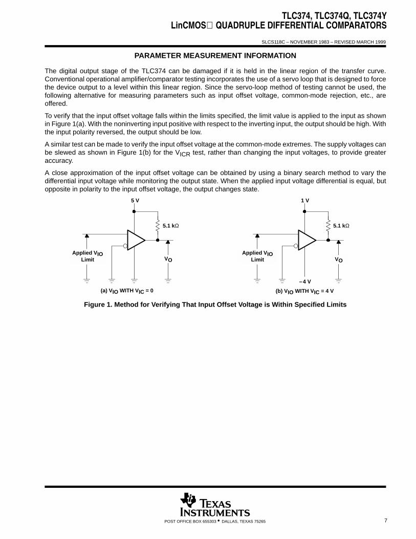
The digital output stage of the TLC374 can be damaged if it is held in the linear region of the transfer curve.Conventional operational amplifier/comparator testing incorporates the use of a servo loop that is designed to forcethe device output to a level within this linear region. Since the servo-loop method of testing cannot be used, thefollowing alternative for measuring parameters such as input offset voltage, common-mode rejection, etc., areoffered.
To verify that the input offset voltage falls within the limits specified, the limit value is applied to the input as shownin Figure 1(a). With the noninverting input positive with respect to the inverting input, the output should be high. Withthe input polarity reversed, the output should be low.
A similar test can be made to verify the input offset voltage at the common-mode extremes. The supply voltages canbe slewed as shown in Figure 1(b) for the VICR test, rather than changing the input voltages, to provide greateraccuracy.
A close approximation of the input offset voltage can be obtained by using a binary search method to vary thedifferential input voltage while monitoring the output state. When the applied input voltage differential is equal, butopposite in polarity to the input offset voltage, the output changes state.
5 V
5.1 kΩ
(a) VIO WITH VIC = 0 (b) VIO WITH VIC = 4 V
Applied VIOLimit VO
1 V
Applied VIOLimit VO
5.1 kΩ
–4 V
Figure 1. Method for Verifying That Input Offset Voltage is Within Specified Limits
TLC374, TLC374Q, TLC374YLinCMOS QUADRUPLE DIFFERENTIAL COMPARATORS
SLCS118C – NOVEMBER 1983 – REVISED MARCH 1999
8 POST OFFICE BOX 655303 • DALLAS, TEXAS 75265
PARAMETER MEASUREMENT INFORMATION
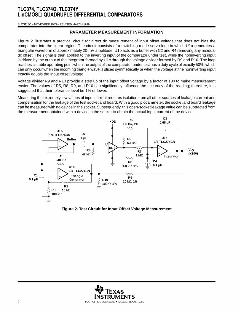
Figure 2 illustrates a practical circuit for direct dc measurement of input offset voltage that does not bias thecomparator into the linear region. The circuit consists of a switching-mode servo loop in which U1a generates atriangular waveform of approximately 20-mV amplitude. U1b acts as a buffer with C2 and R4 removing any residualdc offset. The signal is then applied to the inverting input of the comparator under test, while the noninverting inputis driven by the output of the integrator formed by U1c through the voltage divider formed by R9 and R10. The loopreaches a stable operating point when the output of the comparator under test has a duty cycle of exactly 50%, whichcan only occur when the incoming triangle wave is sliced symmetrically or when the voltage at the noninverting inputexactly equals the input offset voltage.
Voltage divider R9 and R10 provide a step up of the input offset voltage by a factor of 100 to make measurementeasier. The values of R5, R8, R9, and R10 can significantly influence the accuracy of the reading; therefore, it issuggested that their tolerance level be 1% or lower.
Measuring the extremely low values of input current requires isolation from all other sources of leakage current andcompensation for the leakage of the test socket and board. With a good picoammeter, the socket and board leakagecan be measured with no device in the socket. Subsequently, this open-socket leakage value can be subtracted fromthe measurement obtained with a device in the socket to obtain the actual input current of the device.
+
– DUT
+
–
–
+
U1b1/4 TLC274CN
Buffer
C21 µF
R1240 kΩ
U1a1/4 TLC274CN
TriangleGenerator
R210 kΩR3
100 kΩ
C10.1 µF R10
100 Ω, 1%
R910 kΩ, 1%
R81.8 kΩ, 1%
R71 MΩ
R65.1 kΩ
R51.8 kΩ, 1%
C30.68 µF
U1c1/4 TLC274CN
Integrator
C40.1 µF
R447 kΩ
VDD
VIO(X100)
Figure 2. Test Circuit for Input Offset Voltage Measurement
TLC374, TLC374Q, TLC374YLinCMOS QUADRUPLE DIFFERENTIAL COMPARATORS
SLCS118C – NOVEMBER 1983 – REVISED MARCH 1999
9POST OFFICE BOX 655303 • DALLAS, TEXAS 75265
PARAMETER MEASUREMENT INFORMATION
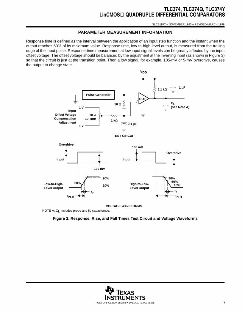
Response time is defined as the interval between the application of an input step function and the instant when theoutput reaches 50% of its maximum value. Response time, low-to-high-level output, is measured from the trailingedge of the input pulse. Response-time measurement at low input signal levels can be greatly affected by the inputoffset voltage. The offset voltage should be balanced by the adjustment at the inverting input (as shown in Figure 3)so that the circuit is just at the transition point. Then a low signal, for example, 105-mV or 5-mV overdrive, causesthe output to change state.
50%
OUT
5.1 kΩ 1 µF
VDD
Pulse Generator
CL(see Note A)
50 Ω
1 kΩ0.1 µF
TEST CIRCUIT
10 Ω10 Turn
1 V
–1 V
InputOffset VoltageCompensation
Adjustment
VOLTAGE WAVEFORMS
tPLH
tr
10%
90%
100 mV
Overdrive
Input
Low-to-High-Level Output
50%
tPLH
tf
10%
90%
100 mV
Overdrive
Input
High-to-Low-Level Output
NOTE A: CL includes probe and jig capacitance.
Figure 3. Response, Rise, and Fall Times Test Circuit and Voltage Waveforms

TLC374, TLC374Q, TLC374YLinCMOS QUADRUPLE DIFFERENTIAL COMPARATORS
SLCS118C – NOVEMBER 1983 – REVISED MARCH 1999
10 POST OFFICE BOX 655303 • DALLAS, TEXAS 75265
PRINCIPLES OF OPERATION
LinCMOS process
LinCMOS process is a linear polysilicon-gate complimentary-MOS process. Primarily designed for single-supply applications, LinCMOS products facilitate the design of a wide range of high-performance analogfunctions from operational amplifiers to complex mixed-mode converters.
While digital designers are experienced with CMOS, MOS technologies are relatively new for analog designers.This short guide is intended to answer the most frequently asked questions related to the quality and reliabilityof LinCMOS products. Further questions should be directed to the nearest TI field sales office.
electrostatic discharge
CMOS circuits are prone to gate oxide breakdown when exposed to high voltages even if the exposure is onlyfor very short periods of time. Electrostatic discharge (ESD) is one of the most common causes of damage toCMOS devices. It can occur when a device is handled without proper consideration for environmentalelectrostatic charges, e.g. during board assembly. If a circuit in which one amplifier from a dual operationalamplifier is being used and the unused pins are left open, high voltages tends to develop. If there is no provisionfor ESD protection, these voltages may eventually punch through the gate oxide and cause the device to fail.To prevent voltage buildup, each pin is protected by internal circuitry.
Standard ESD-protection circuits safely shunt the ESD current by providing a mechanism whereby one or moretransistors break down at voltages higher than normal operating voltages but lower than the breakdown voltageof the input gate. This type of protection scheme is limited by leakage currents which flow through the shuntingtransistors during normal operation after an ESD voltage has occurred. Although these currents are small, onthe order of tens of nanoamps, CMOS amplifiers are often specified to draw input currents as low as tens ofpicoamps.
To overcome this limitation, TI design engineers developed the patented ESD-protection circuit shown inFigure 4. This circuit can withstand several successive 1-kV ESD pulses, while reducing or eliminating leakagecurrents that may be drawn through the input pins. A more detailed discussion of the operation of TI’sESD-protection circuit is presented on the next page.
All input an output pins of LinCMOS and Advanced LinCMOS products have associated ESD-protectioncircuitry that undergoes qualification testing to withstand 1000 V discharged from a 100-pF capacitor througha 1500-Ω resistor (human body model) and 200 V from a 100-pF capacitor with no current-limiting resistor(charged device model). These tests simulate both operator and machine handling of devices during normaltest and assembly operations.
D1 D2
Q2
R2
D3
Q1
R1VDD
To Protected CircuitInput
VSS
Figure 4. LinCMOS ESD-Protection Schematic

TLC374, TLC374Q, TLC374YLinCMOS QUADRUPLE DIFFERENTIAL COMPARATORS
SLCS118C – NOVEMBER 1983 – REVISED MARCH 1999
11POST OFFICE BOX 655303 • DALLAS, TEXAS 75265
PRINCIPLES OF OPERATION
Input protection circuit operation
Texas Instruments patented protection circuitry allows for both positive- and negative-going ESD transients.These transients are characterized by extremely fast rise times and usually low energies, and can occur bothwhen the device has all pins open and when it is installed in a circuit.
positive ESD transients
Initial positive charged energy is shunted through Q1 to VSS. Q1 turns on when the voltage at the input risesabove the voltage on VDD by a value equal to the VEB of Q1. The base current increases through R2 with inputcurrent as Q1 saturates. The base current through R2 as Q1 saturates forces the voltage at the drain and gateof Q2 to exceed its threshold level (VT ∼ 22 to 26 V) and turn on Q2. The shunted input current through Q1 toVSS is now shunted through the n-channel enhancement-type MOSFET Q2 to VSS. If the voltage on the inputpin continues to rise, the breakdown voltage of d3 is exceeded and all remaining energy is dissipated in R1 andD3. The breakdown voltage of D3 is designed to be 24 V to 27 V, which is well below the gate oxide voltage ofthe circuit to be protected.
negative ESD transients
The negative charged ESD transients are shunted directly through D1. Additional energy is dissipated in R1and D2 as D2 becomes forward-biased. The voltage seen by the protected circuit is –0.3 V to –1 V (the forwardvoltage of D1 and D2).
circuit-design considerations
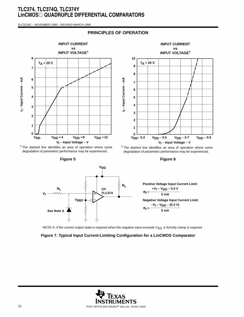
LinCMOS products are being used in actual circuits environments that have input voltages that exceed therecommended common-mode input voltage range and activate the input protection circuit. Even under normaloperation, these conditions occur during circuit power up or power down, and in many cases, when the deviceis being used for a signal conditioning function. The input voltages can exceed VICR and not damage the deviceonly if the inputs are current limited. The recommended current limit shown on most product data sheets is±5 mA. Figures 5 and 6 show typical characteristics for input voltage vs input current.
Normal operation and correct output state can be expected even when the input voltage exceeds the positivesupply voltage. The input current should be externally limited even through internal positive current limiting isachieved in the input protection circuit by the action of Q1. When Q1 is on, it saturates and limits the currentto approximately 5-mA collector current by design. When saturated, Q1 base current increases with inputcurrent. This current is forced into the VDD pin and into the device IDD or the VDD supply through R2 producingthe current limiting effects shown in Figure 5. This internal limiting lasts only as long as the input voltage is belowthe VT of Q2.
When the input voltage exceeds the negative supply voltage, normal operation is affected and output voltagestates may not be correct. Also, the isolation between channels of multiple devices (duals and quads) can beseverely affected. External current limiting must be used since this current is directly shunted by D1 and D2,and no internal limiting is achieved. If normal output voltage states are required, an external input voltage clampis required (see Figure 7).
TLC374, TLC374Q, TLC374YLinCMOS QUADRUPLE DIFFERENTIAL COMPARATORS
SLCS118C – NOVEMBER 1983 – REVISED MARCH 1999
12 POST OFFICE BOX 655303 • DALLAS, TEXAS 75265
PRINCIPLES OF OPERATION
Figure 5
3
2
1
0
4
5
6
7
8
II –
Inp
ut
Cu
rren
t –
mA
I I
INPUT CURRENTvs
INPUT VOLTAGE†
VI – Input Voltage – V
VDD VDD +4 VDD +8 VDD +12
TA = 25°C
† The dashed line identifies an area of operation where somedegradation of parametric performance may be experienced.
Figure 6
3
2
1
0
4
5
6
7
8
II –
Inp
ut
Cu
rren
t –
mA
I I
INPUT CURRENTvs
INPUT VOLTAGE†
VI – Input Voltage – V
VDD– 0.3 VDD – 0.5 VDD – 0.7 VDD – 0.9
TA = 25°C9
10
† The dashed line identifies an area of operation where somedegradation of parametric performance may be experienced.
See Note A
5 mA+
–
RL
VDD
1/4TLC374
RL
VREF
VI
+VI – VDD – 0.3 VRI =
Positive Voltage Input Current Limit:
5 mA
–VI – VDD – (0.3 V)RI =
Negative Voltage Input Current Limit:
NOTE A: If the correct output state is required when the negative input exceeds VSS, a Schotty clamp is required.
Figure 7. Typical Input Current-Limiting Configuration for a LinCMOS Comparator
PACKAGE OPTION ADDENDUM
www.ti.com 24-Aug-2018
Addendum-Page 1
PACKAGING INFORMATION
Orderable Device Status(1)
Package Type PackageDrawing
Pins PackageQty
Eco Plan(2)
Lead/Ball Finish(6)
MSL Peak Temp(3)
Op Temp (°C) Device Marking(4/5)
Samples
5962-87659012A ACTIVE LCCC FK 20 1 TBD POST-PLATE N / A for Pkg Type -55 to 125 5962-87659012ATLC374MFKB
5962-8765901CA ACTIVE CDIP J 14 1 TBD A42 N / A for Pkg Type -55 to 125 5962-8765901CATLC374MJB
TLC374CD ACTIVE SOIC D 14 50 Green (RoHS& no Sb/Br)
CU NIPDAU Level-1-260C-UNLIM 0 to 70 TLC374C
TLC374CDG4 ACTIVE SOIC D 14 50 Green (RoHS& no Sb/Br)
CU NIPDAU Level-1-260C-UNLIM 0 to 70 TLC374C
TLC374CDR ACTIVE SOIC D 14 2500 Green (RoHS& no Sb/Br)
CU NIPDAU Level-1-260C-UNLIM 0 to 70 TLC374C
TLC374CDRG4 ACTIVE SOIC D 14 2500 Green (RoHS& no Sb/Br)
CU NIPDAU Level-1-260C-UNLIM 0 to 70 TLC374C
TLC374CN ACTIVE PDIP N 14 25 Green (RoHS& no Sb/Br)
CU NIPDAU N / A for Pkg Type 0 to 70 TLC374CN
TLC374CN-A ACTIVE PDIP N 14 25 Green (RoHS& no Sb/Br)
CU NIPDAU N / A for Pkg Type 0 to 70 TLC374CN_A
TLC374CNE4 ACTIVE PDIP N 14 25 Green (RoHS& no Sb/Br)
CU NIPDAU N / A for Pkg Type 0 to 70 TLC374CN
TLC374CPW ACTIVE TSSOP PW 14 90 Green (RoHS& no Sb/Br)
CU NIPDAU Level-1-260C-UNLIM 0 to 70 P374
TLC374CPWR ACTIVE TSSOP PW 14 2000 Green (RoHS& no Sb/Br)
CU NIPDAU Level-1-260C-UNLIM 0 to 70 P374
TLC374ID ACTIVE SOIC D 14 50 Green (RoHS& no Sb/Br)
CU NIPDAU Level-1-260C-UNLIM -40 to 85 TLC374I
TLC374IDR ACTIVE SOIC D 14 2500 Green (RoHS& no Sb/Br)
CU NIPDAU Level-1-260C-UNLIM -40 to 85 TLC374I
TLC374IDRG4 ACTIVE SOIC D 14 2500 Green (RoHS& no Sb/Br)
CU NIPDAU Level-1-260C-UNLIM -40 to 85 TLC374I
TLC374IN ACTIVE PDIP N 14 25 Green (RoHS& no Sb/Br)
CU NIPDAU N / A for Pkg Type -40 to 85 TLC374IN
TLC374MD ACTIVE SOIC D 14 50 Green (RoHS& no Sb/Br)
CU NIPDAU Level-1-260C-UNLIM -55 to 125 TLC374M

PACKAGE OPTION ADDENDUM
www.ti.com 24-Aug-2018
Addendum-Page 2
Orderable Device Status(1)
Package Type PackageDrawing
Pins PackageQty
Eco Plan(2)
Lead/Ball Finish(6)
MSL Peak Temp(3)
Op Temp (°C) Device Marking(4/5)
Samples
TLC374MDG4 ACTIVE SOIC D 14 50 Green (RoHS& no Sb/Br)
CU NIPDAU Level-1-260C-UNLIM TLC374M
TLC374MFKB ACTIVE LCCC FK 20 1 TBD POST-PLATE N / A for Pkg Type -55 to 125 5962-87659012ATLC374MFKB
TLC374MJ ACTIVE CDIP J 14 1 TBD A42 N / A for Pkg Type -55 to 125 TLC374MJ
TLC374MJB ACTIVE CDIP J 14 1 TBD A42 N / A for Pkg Type -55 to 125 5962-8765901CATLC374MJB
(1) The marketing status values are defined as follows:ACTIVE: Product device recommended for new designs.LIFEBUY: TI has announced that the device will be discontinued, and a lifetime-buy period is in effect.NRND: Not recommended for new designs. Device is in production to support existing customers, but TI does not recommend using this part in a new design.PREVIEW: Device has been announced but is not in production. Samples may or may not be available.OBSOLETE: TI has discontinued the production of the device.
(2) RoHS: TI defines "RoHS" to mean semiconductor products that are compliant with the current EU RoHS requirements for all 10 RoHS substances, including the requirement that RoHS substancedo not exceed 0.1% by weight in homogeneous materials. Where designed to be soldered at high temperatures, "RoHS" products are suitable for use in specified lead-free processes. TI mayreference these types of products as "Pb-Free".RoHS Exempt: TI defines "RoHS Exempt" to mean products that contain lead but are compliant with EU RoHS pursuant to a specific EU RoHS exemption.Green: TI defines "Green" to mean the content of Chlorine (Cl) and Bromine (Br) based flame retardants meet JS709B low halogen requirements of <=1000ppm threshold. Antimony trioxide basedflame retardants must also meet the <=1000ppm threshold requirement.
(3) MSL, Peak Temp. - The Moisture Sensitivity Level rating according to the JEDEC industry standard classifications, and peak solder temperature.
(4) There may be additional marking, which relates to the logo, the lot trace code information, or the environmental category on the device.
(5) Multiple Device Markings will be inside parentheses. Only one Device Marking contained in parentheses and separated by a "~" will appear on a device. If a line is indented then it is a continuationof the previous line and the two combined represent the entire Device Marking for that device.
(6) Lead/Ball Finish - Orderable Devices may have multiple material finish options. Finish options are separated by a vertical ruled line. Lead/Ball Finish values may wrap to two lines if the finishvalue exceeds the maximum column width.
Important Information and Disclaimer:The information provided on this page represents TI's knowledge and belief as of the date that it is provided. TI bases its knowledge and belief on informationprovided by third parties, and makes no representation or warranty as to the accuracy of such information. Efforts are underway to better integrate information from third parties. TI has taken andcontinues to take reasonable steps to provide representative and accurate information but may not have conducted destructive testing or chemical analysis on incoming materials and chemicals.TI and TI suppliers consider certain information to be proprietary, and thus CAS numbers and other limited information may not be available for release.
PACKAGE OPTION ADDENDUM
www.ti.com 24-Aug-2018
Addendum-Page 3
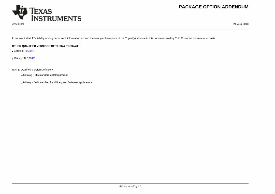
In no event shall TI's liability arising out of such information exceed the total purchase price of the TI part(s) at issue in this document sold by TI to Customer on an annual basis.
OTHER QUALIFIED VERSIONS OF TLC374, TLC374M :
• Catalog: TLC374
• Military: TLC374M
NOTE: Qualified Version Definitions:
• Catalog - TI's standard catalog product
• Military - QML certified for Military and Defense Applications

TAPE AND REEL INFORMATION
*All dimensions are nominal
Device PackageType
PackageDrawing
Pins SPQ ReelDiameter
(mm)
ReelWidth
W1 (mm)
A0(mm)
B0(mm)
K0(mm)
P1(mm)
W(mm)
Pin1Quadrant
TLC374CDR SOIC D 14 2500 330.0 16.4 6.5 9.0 2.1 8.0 16.0 Q1
TLC374CPWR TSSOP PW 14 2000 330.0 12.4 6.9 5.6 1.6 8.0 12.0 Q1
TLC374IDR SOIC D 14 2500 330.0 16.4 6.5 9.0 2.1 8.0 16.0 Q1
PACKAGE MATERIALS INFORMATION
www.ti.com 24-Aug-2017
Pack Materials-Page 1

*All dimensions are nominal
Device Package Type Package Drawing Pins SPQ Length (mm) Width (mm) Height (mm)
TLC374CDR SOIC D 14 2500 333.2 345.9 28.6
TLC374CPWR TSSOP PW 14 2000 367.0 367.0 35.0
TLC374IDR SOIC D 14 2500 367.0 367.0 38.0
PACKAGE MATERIALS INFORMATION
www.ti.com 24-Aug-2017
Pack Materials-Page 2

www.ti.com
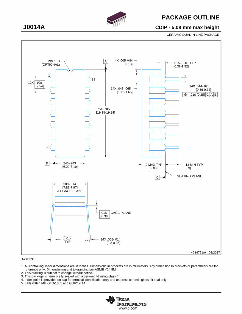
PACKAGE OUTLINE
C
14X .008-.014 [0.2-0.36]TYP
-150
AT GAGE PLANE
-.314.308-7.977.83[ ]
14X -.026.014-0.660.36[ ]14X -.065.045
-1.651.15[ ]
.2 MAX TYP[5.08]
.13 MIN TYP[3.3]
TYP-.060.015-1.520.38[ ]
4X .005 MIN[0.13]
12X .100[2.54]
.015 GAGE PLANE[0.38]
A
-.785.754-19.9419.15[ ]
B -.283.245-7.196.22[ ]
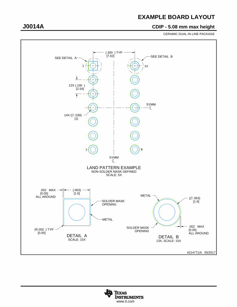
CDIP - 5.08 mm max heightJ0014ACERAMIC DUAL IN LINE PACKAGE
4214771/A 05/2017
NOTES: 1. All controlling linear dimensions are in inches. Dimensions in brackets are in millimeters. Any dimension in brackets or parenthesis are for reference only. Dimensioning and tolerancing per ASME Y14.5M.2. This drawing is subject to change without notice. 3. This package is hermitically sealed with a ceramic lid using glass frit.4. Index point is provided on cap for terminal identification only and on press ceramic glass frit seal only.5. Falls within MIL-STD-1835 and GDIP1-T14.
7 8
141
PIN 1 ID(OPTIONAL)
SCALE 0.900
SEATING PLANE
.010 [0.25] C A B
www.ti.com
EXAMPLE BOARD LAYOUT
ALL AROUND[0.05]
MAX.002
.002 MAX[0.05]ALL AROUND
SOLDER MASKOPENING
METAL
(.063)[1.6]
(R.002 ) TYP[0.05]
14X ( .039)[1]
( .063)[1.6]
12X (.100 )[2.54]
(.300 ) TYP[7.62]
CDIP - 5.08 mm max heightJ0014ACERAMIC DUAL IN LINE PACKAGE
4214771/A 05/2017
LAND PATTERN EXAMPLENON-SOLDER MASK DEFINED
SCALE: 5X
SEE DETAIL A SEE DETAIL B
SYMM
SYMM
1
7 8
14
DETAIL ASCALE: 15X
SOLDER MASKOPENING
METAL
DETAIL B13X, SCALE: 15X

IMPORTANT NOTICE
Texas Instruments Incorporated (TI) reserves the right to make corrections, enhancements, improvements and other changes to itssemiconductor products and services per JESD46, latest issue, and to discontinue any product or service per JESD48, latest issue. Buyersshould obtain the latest relevant information before placing orders and should verify that such information is current and complete.TI’s published terms of sale for semiconductor products (http://www.ti.com/sc/docs/stdterms.htm) apply to the sale of packaged integratedcircuit products that TI has qualified and released to market. Additional terms may apply to the use or sale of other types of TI products andservices.Reproduction of significant portions of TI information in TI data sheets is permissible only if reproduction is without alteration and isaccompanied by all associated warranties, conditions, limitations, and notices. TI is not responsible or liable for such reproduceddocumentation. Information of third parties may be subject to additional restrictions. Resale of TI products or services with statementsdifferent from or beyond the parameters stated by TI for that product or service voids all express and any implied warranties for theassociated TI product or service and is an unfair and deceptive business practice. TI is not responsible or liable for any such statements.Buyers and others who are developing systems that incorporate TI products (collectively, “Designers”) understand and agree that Designersremain responsible for using their independent analysis, evaluation and judgment in designing their applications and that Designers havefull and exclusive responsibility to assure the safety of Designers' applications and compliance of their applications (and of all TI productsused in or for Designers’ applications) with all applicable regulations, laws and other applicable requirements. Designer represents that, withrespect to their applications, Designer has all the necessary expertise to create and implement safeguards that (1) anticipate dangerousconsequences of failures, (2) monitor failures and their consequences, and (3) lessen the likelihood of failures that might cause harm andtake appropriate actions. Designer agrees that prior to using or distributing any applications that include TI products, Designer willthoroughly test such applications and the functionality of such TI products as used in such applications.TI’s provision of technical, application or other design advice, quality characterization, reliability data or other services or information,including, but not limited to, reference designs and materials relating to evaluation modules, (collectively, “TI Resources”) are intended toassist designers who are developing applications that incorporate TI products; by downloading, accessing or using TI Resources in anyway, Designer (individually or, if Designer is acting on behalf of a company, Designer’s company) agrees to use any particular TI Resourcesolely for this purpose and subject to the terms of this Notice.TI’s provision of TI Resources does not expand or otherwise alter TI’s applicable published warranties or warranty disclaimers for TIproducts, and no additional obligations or liabilities arise from TI providing such TI Resources. TI reserves the right to make corrections,enhancements, improvements and other changes to its TI Resources. TI has not conducted any testing other than that specificallydescribed in the published documentation for a particular TI Resource.Designer is authorized to use, copy and modify any individual TI Resource only in connection with the development of applications thatinclude the TI product(s) identified in such TI Resource. NO OTHER LICENSE, EXPRESS OR IMPLIED, BY ESTOPPEL OR OTHERWISETO ANY OTHER TI INTELLECTUAL PROPERTY RIGHT, AND NO LICENSE TO ANY TECHNOLOGY OR INTELLECTUAL PROPERTYRIGHT OF TI OR ANY THIRD PARTY IS GRANTED HEREIN, including but not limited to any patent right, copyright, mask work right, orother intellectual property right relating to any combination, machine, or process in which TI products or services are used. Informationregarding or referencing third-party products or services does not constitute a license to use such products or services, or a warranty orendorsement thereof. Use of TI Resources may require a license from a third party under the patents or other intellectual property of thethird party, or a license from TI under the patents or other intellectual property of TI.TI RESOURCES ARE PROVIDED “AS IS” AND WITH ALL FAULTS. TI DISCLAIMS ALL OTHER WARRANTIES ORREPRESENTATIONS, EXPRESS OR IMPLIED, REGARDING RESOURCES OR USE THEREOF, INCLUDING BUT NOT LIMITED TOACCURACY OR COMPLETENESS, TITLE, ANY EPIDEMIC FAILURE WARRANTY AND ANY IMPLIED WARRANTIES OFMERCHANTABILITY, FITNESS FOR A PARTICULAR PURPOSE, AND NON-INFRINGEMENT OF ANY THIRD PARTY INTELLECTUALPROPERTY RIGHTS. TI SHALL NOT BE LIABLE FOR AND SHALL NOT DEFEND OR INDEMNIFY DESIGNER AGAINST ANY CLAIM,INCLUDING BUT NOT LIMITED TO ANY INFRINGEMENT CLAIM THAT RELATES TO OR IS BASED ON ANY COMBINATION OFPRODUCTS EVEN IF DESCRIBED IN TI RESOURCES OR OTHERWISE. IN NO EVENT SHALL TI BE LIABLE FOR ANY ACTUAL,DIRECT, SPECIAL, COLLATERAL, INDIRECT, PUNITIVE, INCIDENTAL, CONSEQUENTIAL OR EXEMPLARY DAMAGES INCONNECTION WITH OR ARISING OUT OF TI RESOURCES OR USE THEREOF, AND REGARDLESS OF WHETHER TI HAS BEENADVISED OF THE POSSIBILITY OF SUCH DAMAGES.Unless TI has explicitly designated an individual product as meeting the requirements of a particular industry standard (e.g., ISO/TS 16949and ISO 26262), TI is not responsible for any failure to meet such industry standard requirements.Where TI specifically promotes products as facilitating functional safety or as compliant with industry functional safety standards, suchproducts are intended to help enable customers to design and create their own applications that meet applicable functional safety standardsand requirements. Using products in an application does not by itself establish any safety features in the application. Designers mustensure compliance with safety-related requirements and standards applicable to their applications. Designer may not use any TI products inlife-critical medical equipment unless authorized officers of the parties have executed a special contract specifically governing such use.Life-critical medical equipment is medical equipment where failure of such equipment would cause serious bodily injury or death (e.g., lifesupport, pacemakers, defibrillators, heart pumps, neurostimulators, and implantables). Such equipment includes, without limitation, allmedical devices identified by the U.S. Food and Drug Administration as Class III devices and equivalent classifications outside the U.S.TI may expressly designate certain products as completing a particular qualification (e.g., Q100, Military Grade, or Enhanced Product).Designers agree that it has the necessary expertise to select the product with the appropriate qualification designation for their applicationsand that proper product selection is at Designers’ own risk. Designers are solely responsible for compliance with all legal and regulatoryrequirements in connection with such selection.Designer will fully indemnify TI and its representatives against any damages, costs, losses, and/or liabilities arising out of Designer’s non-compliance with the terms and provisions of this Notice.
Mailing Address: Texas Instruments, Post Office Box 655303, Dallas, Texas 75265Copyright © 2018, Texas Instruments Incorporated