tlv6710 micropower, 36-v window comparator with 400 … · vdd = 5 v, iout = 5 ma 150 250 mv iin...
TRANSCRIPT

VPULL-UP
(Up To 36 V)
INA+
GND
INB–
VDD
OUTA
OUTB
Reference
1.8 V to 36 V
Product
Folder
Order
Now
Technical
Documents
Tools &
Software
Support &Community
An IMPORTANT NOTICE at the end of this data sheet addresses availability, warranty, changes, use in safety-critical applications,intellectual property matters and other important disclaimers. PRODUCTION DATA.
TLV6710SNVSAV4A –JANUARY 2018–REVISED APRIL 2018
TLV6710 Micropower, 36-V Window Comparator With 400-mV Reference
1
1 Features1• High Supply Voltage Range: 1.8 V to 36 V• Adjustable Threshold: Down to 400 mV• High Threshold Accuracy:
– 0.25% (Typ)– 0.75% Max Over Temperature
• Low Quiescent Current: 7 µA (Typ)• Open-Drain Outputs• Internal Hysteresis: 5.5 mV (Typ)• Temperature Range: –40°C to 125°C• Package: Thin SOT-23-6
2 Applications• Notebook PCs and Tablets• Smartphones• Digital Cameras• Video Game Controllers• Relays and Circuit Breakers• Portable Medical Devices• Door and Window Sensors• Portable- and Battery-Powered Products
3 DescriptionThe TLV6710 is a high voltage window comparatorthat operates over a 1.8 V to 36 V range. The devicehas two high-accuracy comparators with an internal400-mV reference and two open-drain outputs ratedto 36 V. The TLV6710 can be used as a windowcomparator or as two independent comparators; themonitored voltage can be set with the use of externalresistors.
OUTA is driven low when the voltage at INA+ dropsbelow (VITP – VHYS), and goes high when the voltagereturns above the respective threshold (VITP). OUTBis driven low when the voltage at INB– rises aboveVITP, and goes high when the voltage drops below therespective threshold (VITP – VHYS). Both comparatorsin the TLV6710 include built-in hysteresis to rejectbrief glitches, thereby ensuring stable outputoperation without false triggering.
The TLV6710 is available in a Thin SOT-23-6package and is specified over the junctiontemperature range of –40°C to 125°C.
Device Information(1)
PART NUMBER PACKAGE BODY SIZE (NOM)TLV6710 SOT-23 (6) 2.90 mm × 1.60 mm
(1) For all available packages, see the package option addendumat the end of the data sheet.
Simplified Block Diagram
2
TLV6710SNVSAV4A –JANUARY 2018–REVISED APRIL 2018 www.ti.com
Product Folder Links: TLV6710
Submit Documentation Feedback Copyright © 2018, Texas Instruments Incorporated
Table of Contents1 Features .................................................................. 12 Applications ........................................................... 13 Description ............................................................. 14 Revision History..................................................... 25 Device Comparison Table ..................................... 26 Pin Configuration and Functions ......................... 37 Specifications......................................................... 4
7.1 Absolute Maximum Ratings ..................................... 47.2 ESD Ratings.............................................................. 47.3 Recommended Operating Conditions....................... 47.4 Thermal Information .................................................. 47.5 Electrical Characteristics........................................... 57.6 Timing Requirements ................................................ 67.7 Typical Characteristics .............................................. 7
8 Detailed Description ............................................ 108.1 Overview ................................................................. 108.2 Functional Block Diagram ....................................... 108.3 Feature Description................................................. 11
8.4 Device Functional Modes........................................ 119 Application and Implementation ........................ 12
9.1 Application Information............................................ 129.2 Typical Application ................................................. 159.3 Do's and Don'ts....................................................... 17
10 Power Supply Recommendations ..................... 1811 Layout................................................................... 19
11.1 Layout Guidelines ................................................. 1911.2 Layout Example .................................................... 19
12 Device and Documentation Support ................. 2012.1 Device Support...................................................... 2012.2 Receiving Notification of Documentation Updates 2012.3 Community Resources.......................................... 2012.4 Trademarks ........................................................... 2012.5 Electrostatic Discharge Caution............................ 2012.6 Glossary ................................................................ 20
13 Mechanical, Packaging, and OrderableInformation ........................................................... 20
4 Revision History
Changes from Original (January 2018) to Revision A Page
• Changed Advance Information to Production Data ............................................................................................................... 1
5 Device Comparison Table
Table 1. TLV67xx Integrated Comparator Family
PART NUMBER CONFIGURATION OPERATINGVOLTAGE RANGE
THRESHOLD ACCURACY OVERTEMPERATURE
TLV6700 Window 1.8V to 18V 1%TLV6703 Non-Inverting Single Channel 1.8V to 18V 1%TLV6710 Window 1.8V to 36V 0.75%TLV6713 Non-Inverting Single Channel 1.8V to 36V 0.75%

1
2
3
6
5
4
OUTB
VDD
INB
OUTA
GND
INA
3
TLV6710www.ti.com SNVSAV4A –JANUARY 2018–REVISED APRIL 2018
Product Folder Links: TLV6710
Submit Documentation FeedbackCopyright © 2018, Texas Instruments Incorporated
6 Pin Configuration and Functions
DDC PackageSOT-6
(Top View)
Pin FunctionsPIN
I/O DESCRIPTIONNAME NO.GND 2 — Ground
INA 3 IComparator A input. This pin is connected to the voltage to be monitored with the use of anexternal resistor divider. When the voltage at this terminal drops below the threshold voltageVIT–(INA), OUTA is driven low.
INB 4 IComparator B input. This pin is connected to the voltage to be monitored with the use of anexternal resistor divider. When the voltage at this terminal exceeds the threshold voltageVIT+(INB), OUTB is driven low.
OUTA 1 O INA comparator open-drain output. OUTA is driven low when the voltage at this comparatoris less than VIT–(INA). The output goes high when the sense voltage rises above VIT+(INA).
OUTB 6 O INB comparator open-drain output. OUTB is driven low when the voltage at this comparatorexceeds VIT+(INB). The output goes high when the sense voltage falls below VIT–(INB).
VDD 5 I Supply voltage input. Connect a 1.8-V to 36-V supply to VDD to power the device. It is goodanalog design practice to place a 0.1-µF ceramic capacitor close to this pin.

4
TLV6710SNVSAV4A –JANUARY 2018–REVISED APRIL 2018 www.ti.com
Product Folder Links: TLV6710
Submit Documentation Feedback Copyright © 2018, Texas Instruments Incorporated
(1) Stresses beyond those listed under Absolute Maximum Ratings may cause permanent damage to the device. These are stress ratingsonly, which do not imply functional operation of the device at these or any other conditions beyond those indicated under RecommendedOperating Conditions. Exposure to absolute-maximum-rated conditions for extended periods may affect device reliability.
(2) All voltages are with respect to network ground terminal.
7 Specifications
7.1 Absolute Maximum RatingsOver operating junction temperature range, unless otherwise noted. (1)
MIN MAX UNIT
Voltage (2)
VDD –0.3 +40 VVOUTA, VOUTB –0.3 +28 VVINA, VINB –0.3 +7 V
Current Output pin current 40 mA
TemperatureOperating junction, TJ –40 +125 °CStorage temperature, Tstg –65 +150 °C
(1) JEDEC document JEP155 states that 500-V HBM allows safe manufacturing with a standard ESD control process.(2) JEDEC document JEP157 states that 250-V CDM allows safe manufacturing with a standard ESD control process.
7.2 ESD RatingsVALUE UNIT
V(ESD) Electrostatic dischargeHuman-body model (HBM), per ANSI/ESDA/JEDEC JS-001 (1) ±2000
VCharged-device model (CDM), per JEDEC specification JESD22-C101 (2) ±500
7.3 Recommended Operating Conditionsover operating junction temperature range (unless otherwise noted)
MIN NOM MAX UNITVDD Supply pin voltage 1.8 36 VVINA, VINB Input pin voltage 0 1.7 VVOUTA, VOUTB Output pin voltage 0 25 VIOUTA, IOUTB Output pin current 0 10 mATJ Junction temperature –40 +25 +125 °C
(1) For more information about traditional and new thermal metrics, see the Semiconductor and IC Package Thermal Metrics applicationreport.
7.4 Thermal Information
THERMAL METRIC (1)TLV6710
UNITSDDC (SOT)6 PINS
RθJA Junction-to-ambient thermal resistance 201.6 °C/WRθJC(top) Junction-to-case (top) thermal resistance 47.8 °C/WRθJB Junction-to-board thermal resistance 51.2 °C/WψJT Junction-to-top characterization parameter 0.7 °C/WψJB Junction-to-board characterization parameter 50.8 °C/WRθJC(bot) Junction-to-case (bottom) thermal resistance N/A °C/W

5
TLV6710www.ti.com SNVSAV4A –JANUARY 2018–REVISED APRIL 2018
Product Folder Links: TLV6710
Submit Documentation FeedbackCopyright © 2018, Texas Instruments Incorporated
(1) The lowest supply voltage (VDD) at which output is active; tr(VDD) > 15 µs/V. If less than V(POR), the output is undetermined.(2) When VDD falls below UVLO, OUTA is driven low and OUTB goes to high impedance. The outputs cannot be determined if less than
V(POR).
7.5 Electrical CharacteristicsOver the operating temperature range of TJ = –40°C to +125°C, 1.8 V ≤ VDD < 36 V, and pullup resistors RP1,2 = 100 kΩ,unless otherwise noted. Typical values are at TJ = 25°C and VDD = 12 V.
PARAMETER TEST CONDITIONS MIN TYP MAX UNITVDD Supply voltage range 1.8 36 VV(POR) Power-on reset voltage (1) VOL ≤ 0.2 V 0.8 VVIT–(INA) INA pin negative input threshold voltage VDD = 1.8 V to 36 V 397 400 403 mVVIT+(INA) INA pin positive input threshold voltage VDD = 1.8 V to 36 V 400 405.5 413 mV
VHYS(INA)INA pin hysteresis voltage(HYS = VIT+(INA) – VIT–(INA))
2 5.5 12 mV
VIT–(INB) INB pin negative input threshold voltage VDD = 1.8 V to 36 V 387 394.5 400 mVVIT+(INB) INB pin positive input threshold voltage VDD = 1.8 V to 36 V 397 400 403 mV
VHYS(INB)INB pin hysteresis voltage(HYS = VIT+(INB) – VIT–(INB))
2 5.2 12 mV
VOL Low-level output voltageVDD = 1.8 V, IOUT = 3 mA 130 250 mVVDD = 5 V, IOUT = 5 mA 150 250 mV
IIN Input current (at INA, INB pins)VDD = 1.8 V and 36 V, VINA, VINB = 6.5 V –25 +1 +25 nAVDD = 1.8 V and 36 V, VINA, VINB = 0.1 V –15 +1 +15 nA
ID(leak) Open-drain output leakage current VDD = 1.8 V and 36 V, VOUT = 25 V 10 300 nAIDD Supply current VDD = 1.8 V – 36 V 8 11 µAUVLO Undervoltage lockout (2) VDD falling 1.3 1.5 1.7 V

VDD
INA
OUTA
INB
OUTB
VIT+(INA)
VHYS
VHYS
tpd(LH) tpd(LH)
tpd(LH)
tpd(HL)
tpd(HL)
VIT±(INA)
VIT+(INB)
VIT±(INB)
t d(start)
V(POR)
6
TLV6710SNVSAV4A –JANUARY 2018–REVISED APRIL 2018 www.ti.com
Product Folder Links: TLV6710
Submit Documentation Feedback Copyright © 2018, Texas Instruments Incorporated
(1) High-to-low and low-to-high refers to the transition at the input pins (INA and INB).(2) During power on, VDD must exceed 1.8 V for at least 150 µs (typ) before the output state reflects the input condition.
7.6 Timing RequirementsPARAMETER TEST CONDITION MIN TYP MAX UNIT
.tpd(HL) High-to-low propagation delay (1) VDD = 24 V, ±10-mV input overdrive,RL = 100 kΩ, VOH = 0.9 × VDD, VOL = 250 mV 9.9 µs
tpd(LH) Low-to-high propagation delay (1) VDD = 24 V, ±10-mV input overdrive,RL = 100 kΩ, VOH = 0.9 × VDD, VOL = 250 mV 28.1 µs
td(start)(2) Startup delay VDD = 5 V 155 µs
tr Output rise time VDD = 12 V, 10-mV input overdrive,RL = 100 kΩ, CL = 10 pF, VO = (0.1 to 0.9) × VDD
2.7 µs
tf Output fall time VDD = 12 V, 10-mV input overdrive,RL = 100 kΩ, CL = 10 pF, VO = (0.9 to 0.1) × VDD
0.12 µs
Figure 1. Timing Diagram

TJ (qC)
VIT
+(IN
B) (
mV
)
-40 -20 0 20 40 60 80 100 120 140399.45
399.6
399.75
399.9
400.05
400.2
400.35
D004
VDD = 1.8 VVDD = 12 VVDD = 36 V
TJ (qC)
VIT
-(IN
B) (
mV
)
-40 -20 0 20 40 60 80 100 120 140392.7
393
393.3
393.6
393.9
394.2
394.5
394.8
395.1
395.4
395.7
D003
VDD = 1.8 VVDD = 12 VVDD = 36 V
TJ (qC)
VIT
-(IN
B) (
mV
)
-40 -20 0 20 40 60 80 100 120 140404
404.5
405
405.5
406
406.5
407
407.5
408
408.5
D005
VDD = 1.8 VVDD = 12 VVDD = 36 V
TJ (qC)
VIT
-(IN
A) (
mV
)
-40 -20 0 20 40 60 80 100 120 140399.3
399.45
399.6
399.75
399.9
400.05
400.2
D002
VDD = 1.8 VVDD = 12 VVDD = 36 V
Supply Voltage (V)
Sup
ply
Cur
rent
(P
A)
0 6 12 18 24 30 360
2
4
6
8
10
D001
TJ = -40qCTJ = 0qCTJ = 25qCTJ = 85qCTJ = 125qC
Overdrive (%)
Min
imum
Pul
se W
idth
(P
s)
0 5 10 15 20 25 30 35 40 45 500
2
4
6
8
10
12
14
16
18
20
22
D011
INAINB
7
TLV6710www.ti.com SNVSAV4A –JANUARY 2018–REVISED APRIL 2018
Product Folder Links: TLV6710
Submit Documentation FeedbackCopyright © 2018, Texas Instruments Incorporated
(1) Minimum pulse duration required to trigger output high-to-low transition. INA = negative spike below VIT– and INB = positive spike aboveVIT+.
7.7 Typical CharacteristicsAt TJ = 25°C and VDD = 12 V, unless otherwise noted.
Figure 2. Supply Current vs Supply Voltage
VDD = 24 V
Figure 3. Minimum Pulse Duration vsThreshold Overdrive Voltage (1) (1)
Figure 4. INA Positive Input Threshold Voltage (VIT+(INA)) vsTemperature
Figure 5. INA Negative Input Threshold Voltage (VIT–(INA)) vsTemperature
Figure 6. INB Positive Input Threshold Voltage (VIT+(INB)) vsTemperature
Figure 7. INB Negative Input Threshold Voltage (VIT–(INB)) vsTemperature

TJ (qC)
Hig
h-to
-Low
Pro
paga
tion
Del
ay (P
s)
-40 -20 0 20 40 60 80 100 120 1405
6
7
8
9
10
11
12
D007
VDD = 1.8 V, INA to OUTAVDD = 36 V, INA to OUTAVDD = 1.8 V, INB to OUTBVDD = 36 V, INB to OUTB
TJ (qC)
Low
-to-
Hig
h P
ropa
gatio
n D
elay
(P
s)
-40 -20 0 20 40 60 80 100 120 1401.2
1.5
1.8
2.1
2.4
2.7
3
3.3
D008
VDD = 1.8 V, INA to OUTAVDD = 36 V, INA to OUTAVDD = 1.8 V, INB to OUTBVDD = 36 V, INB to OUTB
VIT+(INB) Threshold Voltage (mV)
Cou
nt
0
500
1000
1500
2000
2500
3000
398
399
400
401
402
D021VIT-(INB) Threshold Voltage (mV)
Cou
nt
0
500
1000
1500
2000
2500
3000
3500
393
394
395
396
397
D023
VIT+(INA) Threshold Voltage (mV)
Cou
nt
0
500
1000
1500
2000
2500
3000
350040
4
405
406
407
408
D022VIT-(INA) Threshold Voltage (mV)
Cou
nt
0
500
1000
1500
2000
2500
3000
3500
4000
4500
398
399
400
401
402
D020
8
TLV6710SNVSAV4A –JANUARY 2018–REVISED APRIL 2018 www.ti.com
Product Folder Links: TLV6710
Submit Documentation Feedback Copyright © 2018, Texas Instruments Incorporated
Typical Characteristics (continued)At TJ = 25°C and VDD = 12 V, unless otherwise noted.
VDD = 1.8 V
Figure 8. INA Positive Input Threshold Voltage (VIT+(INA))Distribution
VDD = 1.8 V
Figure 9. INA Negative Input Threshold Voltage (VIT–(INA))Distribution
VDD = 1.8 V
Figure 10. INB Positive Input Threshold Voltage (VIT+(INB))Distribution
VDD = 1.8 V
Figure 11. INB Negative Input Threshold Voltage (VIT–(INB))Distribution
Input step ±200 mV
Figure 12. Propagation Delay vs Temperature(High-to-Low Transition at the Inputs)
Input step ±200 mV
Figure 13. Propagation Delay vs Temperature(Low-to-High Transition at the Inputs)

Time (50 µs/div)
OUTB (2 V/div)
OUTA (2 V/div)
VDD (2 V/div)
StartupDelayPeriod
TJ (qC)
Sta
rtup
Del
ay (P
s)
-40 -20 0 20 40 60 80 100 120 140120
135
150
165
180
195
210
D025
Time (50 µs/div)
OUTB (2 V/div)
OUTA (2 V/div)
VDD (2 V/div)
StartupDelayPeriod
IOUT (mA)
VO
L (V
)
0 1 2 3 4 5 6 7 8 9 100
0.1
0.2
0.3
0.4
0.5
0.6
D009
TJ = -40qCTJ = 0qCTJ = 25qCTJ = 85qCTJ = 125qC
IOUT (mA)
VO
L (V
)
0 1 2 3 4 5 6 7 8 9 100
0.1
0.2
0.3
0.4
0.5
D010
TJ = -40qCTJ = 0qCTJ = 25qCTJ = 85qCTJ = 125qC
9
TLV6710www.ti.com SNVSAV4A –JANUARY 2018–REVISED APRIL 2018
Product Folder Links: TLV6710
Submit Documentation FeedbackCopyright © 2018, Texas Instruments Incorporated
Typical Characteristics (continued)At TJ = 25°C and VDD = 12 V, unless otherwise noted.
VDD = 1.8 V
Figure 14. Output Voltage Low vs Output Sink Current
VDD = 12 V
Figure 15. Output Voltage Low vs Output Sink Current
VDD = 5 V
Figure 16. Start-Up Delay vs Temperature
VDD = 5 V, VINA = 390 mV, VINB = 410 mV, VPULLUP = 3.3 V
Figure 17. Start-Up Delay
VDD = 5 V, VINA = 410 mV, VINB = 390 mV, VPULLUP = 3.3 V
Figure 18. Start-Up Delay

INA
GND
INB
VDD
OUTA
OUTB
Reference
A
B
10
TLV6710SNVSAV4A –JANUARY 2018–REVISED APRIL 2018 www.ti.com
Product Folder Links: TLV6710
Submit Documentation Feedback Copyright © 2018, Texas Instruments Incorporated
8 Detailed Description
8.1 OverviewThe TLV6710 combines two comparators (referred to as A and B) and a precision reference for overvoltage andundervoltage detection. The TLV6710 features a wide supply voltage range (1.8 V to 36 V) and high-accuracywindow threshold voltages of 400 mV (0.75% over temperature) with built-in hysteresis. The outputs are rated to25 V and can sink up to 10 mA.
Set each input pin (INA, INB) to monitor any voltage above 0.4 V by using an external resistor divider network.Each input pin has very low input leakage current, allowing the use of large resistor dividers without sacrificingsystem accuracy. To form a window comparator, use the two input pins and three resistors (see the WindowComparator Considerations section). In this configuration, the TLV6710 is designed to assert the output signalswhen the monitored voltage is within the window band. Each input can also be used independently. Therelationship between the inputs and the outputs is shown in Table 2. Broad voltage thresholds are supported thatenable the device to be used in a wide array of applications.
Table 2. Truth TableCONDITION OUTPUT OUTPUT STATE
INA > VIT+(INA) OUTA high Output A high impedanceINA < VIT–(INA) OUTA low Output A sinkingINB > VIT+(INB) OUTB low Output B sinkingINB < VIT–(INB) OUTB high Output B high impedance
8.2 Functional Block Diagram

11
TLV6710www.ti.com SNVSAV4A –JANUARY 2018–REVISED APRIL 2018
Product Folder Links: TLV6710
Submit Documentation FeedbackCopyright © 2018, Texas Instruments Incorporated
8.3 Feature Description
8.3.1 Inputs (INA, INB)The TLV6710 combines two comparators with a precision reference voltage. Each comparator has one externalinput; the other input is connected to the internal reference. The rising threshold on INB and the falling thresholdon INA are designed and trimmed to be equal to the reference voltage (400 mV). This configuration optimizes thedevice accuracy when used as a window comparator. Both comparators also have built-in hysteresis that provesimmunity to noise and ensures stable operation.
The comparator inputs swings from ground to 1.7 V (7.0 V absolute maximum), regardless of the device supplyvoltage used. Although not required in most cases, it is good analog design practice to place a 1-nF to 10-nFbypass capacitor at the comparator input for noisy applications in order to reduce sensitivity to transient voltagechanges on the monitored signal.
For comparator A, the corresponding output (OUTA) is driven to logic low when the input INA voltage dropsbelow VIT–(INA). When the voltage exceeds VIT+(INA), OUTA goes to a high-impedance state; see Figure 1.
For comparator B, the corresponding output (OUTB) is driven to logic low when the voltage at input INB exceedsVIT+(INB). When the voltage drops below VIT–(INB) OUTB goes to a high-impedance state; see Figure 1. Together,these two comparators form a window-detection function as described in the Window Comparator Considerationssection.
8.3.2 Outputs (OUTA, OUTB)In a typical TLV6710 application, the outputs are connected to a GPIO input of the processor (such as a digitalsignal processor [DSP], central processing unit [CPU], field-programmable gate array [FPGA], or application-specific integrated circuit [ASIC]).
The TLV6710 provides two open-drain outputs (OUTA and OUTB); use pullup resistors to hold these lines highwhen the output goes to a high-impedance state. Connect pullup resistors to the proper voltage rails to enablethe outputs to be connected to other devices at correct interface voltage levels. The TLV6710 outputs can bepulled up to 25 V, independent of the device supply voltage. To ensure proper voltage levels, give someconsideration when choosing the pullup resistor values. The pullup resistor value is determined by VOL, outputcapacitive loading, and output leakage current (ID(leak)). These values are specified in the ElectricalCharacteristics table. Use wired-OR logic to merge OUTA and OUTB into one logic signal.
Table 2 and the Inputs (INA, INB) section describe how the outputs are asserted or high impedance. SeeFigure 1 for a timing diagram that describes the relationship between threshold voltages and the respectiveoutput.
8.4 Device Functional Modes
8.4.1 Normal Operation (VDD > UVLO)When the voltage on VDD is greater than 1.8 V for at least 155 µs, the OUTA and OUTB signals correspond tothe voltage on INA and INB as listed in Table 2.
8.4.2 Undervoltage Lockout (V(POR) < VDD < UVLO)When the voltage on VDD is less than the device UVLO voltage, and greater than the power-on reset voltage,V(POR), the OUTA and OUTB signals are asserted and high impedance, respectively, regardless of the voltage onINA and INB.
8.4.3 Power On Reset (VDD < V(POR))When the voltage on VDD is lower than the required voltage to internally pull the asserted output to GND(V(POR)), both outputs are in a high-impedance state.
OvervoltageLimit
Undervoltage Limit
VMON
OUTB
OUTA
VMON(OV)
VMON(OV_HYS)
VMON(UV)
VMON(UV_HYS)
R
(2.21 M )1
W
GND
1.8 V to 25 V
OUTA
OUTB
R2
(13.7 k )W
R3
(69.8 k )W
VMON
INA
INB
VDD
Device
RP1
(50 k )W
OUT
VMONUV OV
OU
T
12
TLV6710SNVSAV4A –JANUARY 2018–REVISED APRIL 2018 www.ti.com
Product Folder Links: TLV6710
Submit Documentation Feedback Copyright © 2018, Texas Instruments Incorporated
9 Application and Implementation
NOTEInformation in the following applications sections is not part of the TI componentspecification, and TI does not warrant its accuracy or completeness. TI’s customers areresponsible for determining suitability of components for their purposes. Customers shouldvalidate and test their design implementation to confirm system functionality.
9.1 Application InformationThe TLV6710 device is a wide-supply voltage window comparator that operates over a VDD range of 1.8 V to36V. The device has two high-accuracy comparators with an internal 400-mV reference and two open-drainoutputs rated to 36 V for overvoltage and undervoltage detection. The device can be used either as awindow comparator or as two independent voltage monitors. The monitored voltages are set with the use ofexternal resistors.
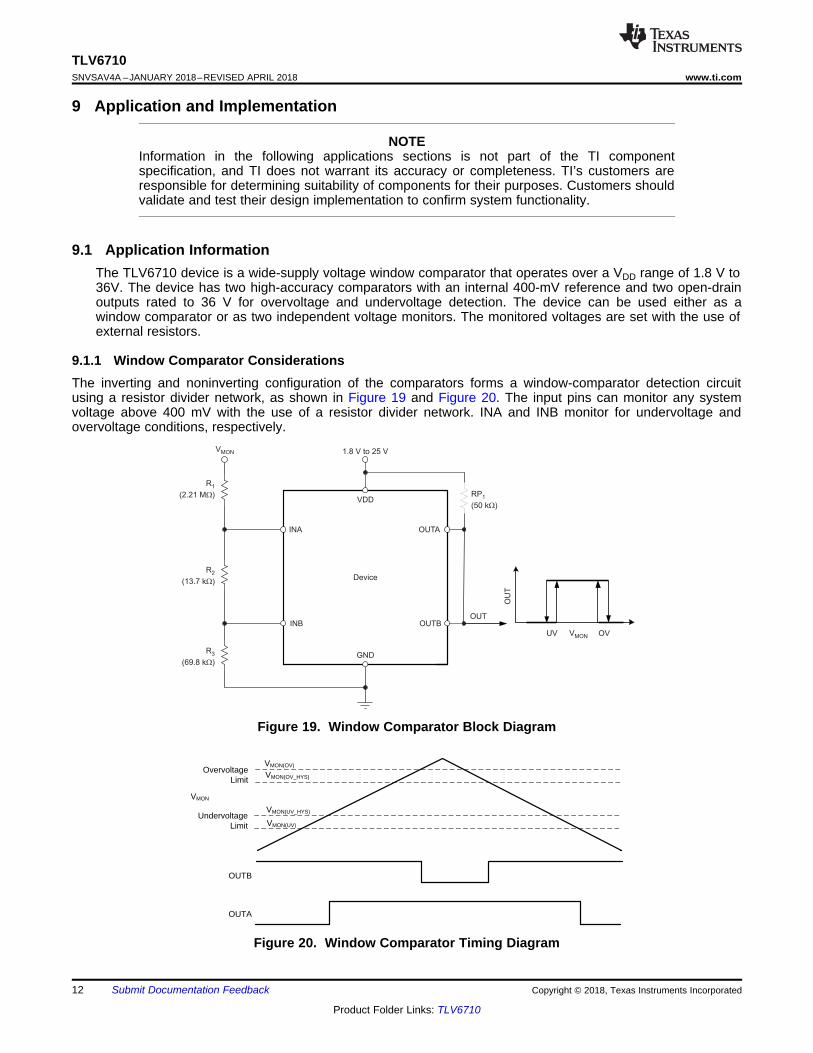
9.1.1 Window Comparator ConsiderationsThe inverting and noninverting configuration of the comparators forms a window-comparator detection circuitusing a resistor divider network, as shown in Figure 19 and Figure 20. The input pins can monitor any systemvoltage above 400 mV with the use of a resistor divider network. INA and INB monitor for undervoltage andovervoltage conditions, respectively.
Figure 19. Window Comparator Block Diagram
Figure 20. Window Comparator Timing Diagram

R =2 - R3VIT (INA)-
R
V
TOTAL
MON(UV)
R =2 - R3VIT+(INA)
R
V
TOTAL
MON(UV_HYS)
R =3 VIT+(INB)
R
V
TOTAL
MON(OV)
13
TLV6710www.ti.com SNVSAV4A –JANUARY 2018–REVISED APRIL 2018
Product Folder Links: TLV6710
Submit Documentation FeedbackCopyright © 2018, Texas Instruments Incorporated
Application Information (continued)The TLV6710 flags the overvoltage or undervoltage condition with the greatest accuracy. The highest accuracythreshold voltages are VIT–(INA) and VIT+(INB), and correspond with the falling undervoltage flag, and the risingovervoltage flag, respectively. These thresholds represent the accuracy when the monitored voltage is within thevalid window (both OUTA and OUTB are in a high-impedance state), and correspond to the VMON(UV) andVMON(OV) trigger voltages, respectively. If the monitored voltage is outside of the valid window (VMON is less thanthe undervoltage limit, VMON(UV), or greater than overvoltage limit, VMON(OV)), then the input threshold voltages tore-enter the valid window are VIT+(INA) or VIT–(INB), and correspond with the VMON(UV_HYS) and VMON(OV_HYS)monitored voltages, respectively.
The resistor divider values and target threshold voltage can be calculated by using Equation 1 throughEquation 4:
RTOTAL = R1 + R2 + R3 (1)
Choose an RTOTAL value so that the current through the divider is approximately 100 times higher than the inputcurrent at the INA and INB pins. Resistors with high values minimize current consumption; however, the inputbias current degrades accuracy if the current through the resistors is too low. See application report SLVA450,Optimizing Resistor Dividers at a Comparator Input, for details on sizing input resistors.
R3 is determined by Equation 2:
where• VMON(OV) is the target voltage at which an overvoltage condition is detected. (2)
R2 is determined by either Equation 3 or Equation 4:
where• VMON(UV_HYS) is the target voltage at which an undervoltage condition is removed as VMON rises. (3)
where• VMON(UV) is the target voltage at which an undervoltage condition is detected. (4)
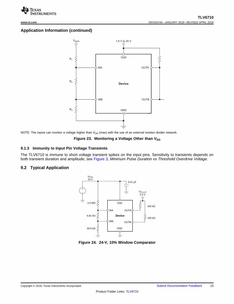
9.1.2 Input and Output ConfigurationsFigure 21 to Figure 23 show examples of the various input and output configurations.

GND
1.8 V to 25 V
OUTA
OUTB
INA
INB
VDD
Device
GND
1.8 V to 36 V
OUTA
OUTB
INA
INB
VDD
Device
V
(up to 25 V)PULLUP
14
TLV6710SNVSAV4A –JANUARY 2018–REVISED APRIL 2018 www.ti.com
Product Folder Links: TLV6710
Submit Documentation Feedback Copyright © 2018, Texas Instruments Incorporated
Application Information (continued)
Figure 21. Interfacing to Voltages Other than VDD
Figure 22. Monitoring the Same Voltage as VDD
Device
+
±
VDD
INA
INB
OUTA
OUTB
GND
2.0 M�
6.81 k�
VPULLUP
3.3 V
30.9 k�
100 k�
100 k�
VMON
24 V0.01 �F
R1
GND
1.8 V to 25 V
OUTA
OUTB
R2
R3
VMON
INA
INB
VDD
Device
15
TLV6710www.ti.com SNVSAV4A –JANUARY 2018–REVISED APRIL 2018
Product Folder Links: TLV6710
Submit Documentation FeedbackCopyright © 2018, Texas Instruments Incorporated
Application Information (continued)
NOTE: The inputs can monitor a voltage higher than VDD (max) with the use of an external resistor divider network.
Figure 23. Monitoring a Voltage Other than VDD
9.1.3 Immunity to Input Pin Voltage TransientsThe TLV6710 is immune to short voltage transient spikes on the input pins. Sensitivity to transients depends onboth transient duration and amplitude; see Figure 3, Minimum Pulse Duration vs Threshold Overdrive Voltage.
9.2 Typical Application
Figure 24. 24-V, 10% Window Comparator

( )( )
( )
.
.IT INB
IT INB RMON OV
V 0 4��$&&� ���72/�9 �������� � ����72/ �������������� � ����� �������
V 26 4�
�
§ · § ·� �¨ ¸ ¨ ¸¨ ¸ © ¹© ¹
1 TOTAL 2 3R R R R 2.03 M �����N �����N �����0 � � � �
( )( )
TOTAL2 IT INA 3
MON UV
R 2.03 MR V R 0.4 V 30.9 k �����N
V 21.6 V� �
: x � x �
R =3 =VIT+(INB)
R
V
TOTAL
MON(OV)
2.03 M
26.4 V
W0.4 V = 30.7 kW
( ).
MON OVTOTAL
V 26.4 VR 2 03 M
I 13 A
P
16
TLV6710SNVSAV4A –JANUARY 2018–REVISED APRIL 2018 www.ti.com
Product Folder Links: TLV6710
Submit Documentation Feedback Copyright © 2018, Texas Instruments Incorporated
Typical Application (continued)9.2.1 Design Requirements
Table 3. Design ParametersPARAMETER DESIGN REQUIREMENT DESIGN RESULT
Monitored voltage
24-V nominal, rising (VMON(OV)) andfalling (VMON(UV)) threshold
±10% nominal (26.4 V and 21.6 V,respectively)
VMON(OV) = 26.4 V ±2.7%, VMON(UV) = 21.6 V ±2.7%
Output logic voltage 3.3-V CMOS 3.3-V CMOSMaximum current consumption 30 µA 24 µA
9.2.2 Detailed Design Procedure1. Determine the minimum total resistance of the resistor network necessary to achieve the current
consumption specification by using Equation 1. For this example, the current flow through the resistornetwork was chosen to be 13 µA; a lower current can be selected, however, care should be taken to avoidleakage currents that are artifacts of the manufacturing process. Leakage currents significantly impact theaccuracy if they are greater than 1% of the resistor network current.
where• VMON(OV) is the target voltage at which an overvoltage condition is detected as VMON rises.• I is the current flowing through the resistor network. (5)
2. After RTOTAL is determined, R3 can be calculated using Equation 6. Select the nearest 1% resistor value forR3. In this case, 30.9 kΩ is the closest value.
(6)3. Use Equation 7 to calculate R2. Select the nearest 1% resistor value for R2. In this case, 6.81 kΩ is the
closest value.
(7)4. Use Equation 8 to calculate R1. Select the nearest 1% resistor value for R1. In this case, 2 MΩ is the closest
value.
(8)5. The worst-case tolerance can be calculated by referring to Equation 13 in application report SLVA450,
Optimizing Resistor Dividers at a Comparator Input. An example of the rising threshold error, VMON(OV), isgiven in Equation 9:
where• % TOL(VIT+(INB)) is the tolerance of the INB positive threshold.• % ACC is the total tolerance of the VMON(OV) voltage.• % TOLR is the tolerance of the resistors selected. (9)
6. When the outputs switch to the high-Z state, the rise time of the OUTA or OUTB node depends on the pullupresistance and the capacitance on the node. Choose pullup resistors that satisfy the downstream timingrequirements; 100-kΩ resistors are a good choice for low-capacitive loads.

Time (5 ms/div)
OUTB (2 V/div)
OUTA (2 V/div)
VDD (10 V/div)
17
TLV6710www.ti.com SNVSAV4A –JANUARY 2018–REVISED APRIL 2018
Product Folder Links: TLV6710
Submit Documentation FeedbackCopyright © 2018, Texas Instruments Incorporated
9.2.3 Application Curves
Figure 25. 24-V Window Monitor Output Response
9.3 Do's and Don'tsIt is good analog design practice to have a 0.1-µF decoupling capacitor from VDD to GND.
If the monitored rail is noisy, connect decoupling capacitors from the comparator inputs to GND.
Do not use resistors for the voltage divider that cause the current through them to be less than 100 times theinput current of the comparators without also accounting for the effect to the accuracy.
Do not use pullup resistors that are too small, because the larger current sunk by the output then exceeds thedesired low-level output voltage (VOL).

100 �
0.01 �F+
±
VDD
INA
INB
OUTA
OUTB
GND
R1
R2
R3
VPULLUP
18
TLV6710SNVSAV4A –JANUARY 2018–REVISED APRIL 2018 www.ti.com
Product Folder Links: TLV6710
Submit Documentation Feedback Copyright © 2018, Texas Instruments Incorporated
10 Power Supply RecommendationsThe TLV6710 has a 40-V absolute maximum rating on the VDD pin, with a recommended operating condition of36 V. If the voltage supply that is providing power to VDD is susceptible to any large voltage transient that mayexceed 40 V, or if the supply exhibits high voltage slew rates greater than 1 V/µs, take additional precautions.Place an RC filter between the supply and VDD to filter any high-frequency transient surges on the VDD pin. A100-Ω resistor and 0.01-µF capacitor is required in these cases, as shown in Figure 26.
Figure 26. Using an RC Filter to Remove High-Frequency Disturbances on VDD

InputSupply
1
2
3 4
6
5
R2R1 R3Monitored
Voltage
RP1 RP2Overvoltage Flag
Undervoltage Flag
PullupVoltage
CVDD
19
TLV6710www.ti.com SNVSAV4A –JANUARY 2018–REVISED APRIL 2018
Product Folder Links: TLV6710
Submit Documentation FeedbackCopyright © 2018, Texas Instruments Incorporated
11 Layout
11.1 Layout Guidelines• Place R1, R2, and R3 close to the device to minimize noise coupling into the INA and INB nodes.• Place the VDD decoupling capacitor close to the device.• Avoid using long traces for the VDD supply node. The VDD capacitor (CVDD), along with parasitic inductance
from the supply to the capacitor, may form an LC tank and create ringing with peak voltages above themaximum VDD voltage. If this is unavoidable, see Figure 26 for an example of filtering VDD.
11.2 Layout Example
Figure 27. Recommended Layout

20
TLV6710SNVSAV4A –JANUARY 2018–REVISED APRIL 2018 www.ti.com
Product Folder Links: TLV6710
Submit Documentation Feedback Copyright © 2018, Texas Instruments Incorporated
12 Device and Documentation Support
12.1 Device Support
12.1.1 Development SupportThe DIP Adapter Evaluation Module allows conversion of the SOT-23-6 package to a standard DIP-6 pinout forease of prototyping and bench evaluation.
12.2 Receiving Notification of Documentation UpdatesTo receive notification of documentation updates, navigate to the device product folder on ti.com. In the upperright corner, click on Alert me to register and receive a weekly digest of any product information that haschanged. For change details, review the revision history included in any revised document.
12.3 Community ResourcesThe following links connect to TI community resources. Linked contents are provided "AS IS" by the respectivecontributors. They do not constitute TI specifications and do not necessarily reflect TI's views; see TI's Terms ofUse.
TI E2E™ Online Community TI's Engineer-to-Engineer (E2E) Community. Created to foster collaborationamong engineers. At e2e.ti.com, you can ask questions, share knowledge, explore ideas and helpsolve problems with fellow engineers.
Design Support TI's Design Support Quickly find helpful E2E forums along with design support tools andcontact information for technical support.
12.4 TrademarksE2E is a trademark of Texas Instruments.All other trademarks are the property of their respective owners.
12.5 Electrostatic Discharge CautionThis integrated circuit can be damaged by ESD. Texas Instruments recommends that all integrated circuits be handled withappropriate precautions. Failure to observe proper handling and installation procedures can cause damage.
ESD damage can range from subtle performance degradation to complete device failure. Precision integrated circuits may be moresusceptible to damage because very small parametric changes could cause the device not to meet its published specifications.
12.6 GlossarySLYZ022 — TI Glossary.
This glossary lists and explains terms, acronyms, and definitions.
13 Mechanical, Packaging, and Orderable InformationThe following pages include mechanical, packaging, and orderable information. This information is the mostcurrent data available for the designated devices. This data is subject to change without notice and revision ofthis document. For browser-based versions of this data sheet, refer to the left-hand navigation.

PACKAGE OPTION ADDENDUM
www.ti.com 16-Apr-2018
Addendum-Page 1
PACKAGING INFORMATION
Orderable Device Status(1)
Package Type PackageDrawing
Pins PackageQty
Eco Plan(2)
Lead/Ball Finish(6)
MSL Peak Temp(3)
Op Temp (°C) Device Marking(4/5)
Samples
TLV6710DDCR ACTIVE SOT-23-THIN DDC 6 3000 Green (RoHS& no Sb/Br)
CU NIPDAU Level-2-260C-1 YEAR -40 to 125 1I61
TLV6710DDCT ACTIVE SOT-23-THIN DDC 6 250 Green (RoHS& no Sb/Br)
CU NIPDAU Level-2-260C-1 YEAR -40 to 125 1I61
(1) The marketing status values are defined as follows:ACTIVE: Product device recommended for new designs.LIFEBUY: TI has announced that the device will be discontinued, and a lifetime-buy period is in effect.NRND: Not recommended for new designs. Device is in production to support existing customers, but TI does not recommend using this part in a new design.PREVIEW: Device has been announced but is not in production. Samples may or may not be available.OBSOLETE: TI has discontinued the production of the device.
(2) RoHS: TI defines "RoHS" to mean semiconductor products that are compliant with the current EU RoHS requirements for all 10 RoHS substances, including the requirement that RoHS substancedo not exceed 0.1% by weight in homogeneous materials. Where designed to be soldered at high temperatures, "RoHS" products are suitable for use in specified lead-free processes. TI mayreference these types of products as "Pb-Free".RoHS Exempt: TI defines "RoHS Exempt" to mean products that contain lead but are compliant with EU RoHS pursuant to a specific EU RoHS exemption.Green: TI defines "Green" to mean the content of Chlorine (Cl) and Bromine (Br) based flame retardants meet JS709B low halogen requirements of <=1000ppm threshold. Antimony trioxide basedflame retardants must also meet the <=1000ppm threshold requirement.
(3) MSL, Peak Temp. - The Moisture Sensitivity Level rating according to the JEDEC industry standard classifications, and peak solder temperature.
(4) There may be additional marking, which relates to the logo, the lot trace code information, or the environmental category on the device.
(5) Multiple Device Markings will be inside parentheses. Only one Device Marking contained in parentheses and separated by a "~" will appear on a device. If a line is indented then it is a continuationof the previous line and the two combined represent the entire Device Marking for that device.
(6) Lead/Ball Finish - Orderable Devices may have multiple material finish options. Finish options are separated by a vertical ruled line. Lead/Ball Finish values may wrap to two lines if the finishvalue exceeds the maximum column width.
Important Information and Disclaimer:The information provided on this page represents TI's knowledge and belief as of the date that it is provided. TI bases its knowledge and belief on informationprovided by third parties, and makes no representation or warranty as to the accuracy of such information. Efforts are underway to better integrate information from third parties. TI has taken andcontinues to take reasonable steps to provide representative and accurate information but may not have conducted destructive testing or chemical analysis on incoming materials and chemicals.TI and TI suppliers consider certain information to be proprietary, and thus CAS numbers and other limited information may not be available for release.
In no event shall TI's liability arising out of such information exceed the total purchase price of the TI part(s) at issue in this document sold by TI to Customer on an annual basis.

PACKAGE OPTION ADDENDUM
www.ti.com 16-Apr-2018
Addendum-Page 2

TAPE AND REEL INFORMATION
*All dimensions are nominal
Device PackageType
PackageDrawing
Pins SPQ ReelDiameter
(mm)
ReelWidth
W1 (mm)
A0(mm)
B0(mm)
K0(mm)
P1(mm)
W(mm)
Pin1Quadrant
TLV6710DDCR SOT-23-THIN
DDC 6 3000 180.0 8.4 3.2 3.2 1.4 4.0 8.0 Q3
TLV6710DDCT SOT-23-THIN
DDC 6 250 180.0 8.4 3.2 3.2 1.4 4.0 8.0 Q3
PACKAGE MATERIALS INFORMATION
www.ti.com 8-May-2018
Pack Materials-Page 1

*All dimensions are nominal
Device Package Type Package Drawing Pins SPQ Length (mm) Width (mm) Height (mm)
TLV6710DDCR SOT-23-THIN DDC 6 3000 195.0 200.0 45.0
TLV6710DDCT SOT-23-THIN DDC 6 250 195.0 200.0 45.0
PACKAGE MATERIALS INFORMATION
www.ti.com 8-May-2018
Pack Materials-Page 2


IMPORTANT NOTICE
Texas Instruments Incorporated (TI) reserves the right to make corrections, enhancements, improvements and other changes to itssemiconductor products and services per JESD46, latest issue, and to discontinue any product or service per JESD48, latest issue. Buyersshould obtain the latest relevant information before placing orders and should verify that such information is current and complete.TI’s published terms of sale for semiconductor products (http://www.ti.com/sc/docs/stdterms.htm) apply to the sale of packaged integratedcircuit products that TI has qualified and released to market. Additional terms may apply to the use or sale of other types of TI products andservices.Reproduction of significant portions of TI information in TI data sheets is permissible only if reproduction is without alteration and isaccompanied by all associated warranties, conditions, limitations, and notices. TI is not responsible or liable for such reproduceddocumentation. Information of third parties may be subject to additional restrictions. Resale of TI products or services with statementsdifferent from or beyond the parameters stated by TI for that product or service voids all express and any implied warranties for theassociated TI product or service and is an unfair and deceptive business practice. TI is not responsible or liable for any such statements.Buyers and others who are developing systems that incorporate TI products (collectively, “Designers”) understand and agree that Designersremain responsible for using their independent analysis, evaluation and judgment in designing their applications and that Designers havefull and exclusive responsibility to assure the safety of Designers' applications and compliance of their applications (and of all TI productsused in or for Designers’ applications) with all applicable regulations, laws and other applicable requirements. Designer represents that, withrespect to their applications, Designer has all the necessary expertise to create and implement safeguards that (1) anticipate dangerousconsequences of failures, (2) monitor failures and their consequences, and (3) lessen the likelihood of failures that might cause harm andtake appropriate actions. Designer agrees that prior to using or distributing any applications that include TI products, Designer willthoroughly test such applications and the functionality of such TI products as used in such applications.TI’s provision of technical, application or other design advice, quality characterization, reliability data or other services or information,including, but not limited to, reference designs and materials relating to evaluation modules, (collectively, “TI Resources”) are intended toassist designers who are developing applications that incorporate TI products; by downloading, accessing or using TI Resources in anyway, Designer (individually or, if Designer is acting on behalf of a company, Designer’s company) agrees to use any particular TI Resourcesolely for this purpose and subject to the terms of this Notice.TI’s provision of TI Resources does not expand or otherwise alter TI’s applicable published warranties or warranty disclaimers for TIproducts, and no additional obligations or liabilities arise from TI providing such TI Resources. TI reserves the right to make corrections,enhancements, improvements and other changes to its TI Resources. TI has not conducted any testing other than that specificallydescribed in the published documentation for a particular TI Resource.Designer is authorized to use, copy and modify any individual TI Resource only in connection with the development of applications thatinclude the TI product(s) identified in such TI Resource. NO OTHER LICENSE, EXPRESS OR IMPLIED, BY ESTOPPEL OR OTHERWISETO ANY OTHER TI INTELLECTUAL PROPERTY RIGHT, AND NO LICENSE TO ANY TECHNOLOGY OR INTELLECTUAL PROPERTYRIGHT OF TI OR ANY THIRD PARTY IS GRANTED HEREIN, including but not limited to any patent right, copyright, mask work right, orother intellectual property right relating to any combination, machine, or process in which TI products or services are used. Informationregarding or referencing third-party products or services does not constitute a license to use such products or services, or a warranty orendorsement thereof. Use of TI Resources may require a license from a third party under the patents or other intellectual property of thethird party, or a license from TI under the patents or other intellectual property of TI.TI RESOURCES ARE PROVIDED “AS IS” AND WITH ALL FAULTS. TI DISCLAIMS ALL OTHER WARRANTIES ORREPRESENTATIONS, EXPRESS OR IMPLIED, REGARDING RESOURCES OR USE THEREOF, INCLUDING BUT NOT LIMITED TOACCURACY OR COMPLETENESS, TITLE, ANY EPIDEMIC FAILURE WARRANTY AND ANY IMPLIED WARRANTIES OFMERCHANTABILITY, FITNESS FOR A PARTICULAR PURPOSE, AND NON-INFRINGEMENT OF ANY THIRD PARTY INTELLECTUALPROPERTY RIGHTS. TI SHALL NOT BE LIABLE FOR AND SHALL NOT DEFEND OR INDEMNIFY DESIGNER AGAINST ANY CLAIM,INCLUDING BUT NOT LIMITED TO ANY INFRINGEMENT CLAIM THAT RELATES TO OR IS BASED ON ANY COMBINATION OFPRODUCTS EVEN IF DESCRIBED IN TI RESOURCES OR OTHERWISE. IN NO EVENT SHALL TI BE LIABLE FOR ANY ACTUAL,DIRECT, SPECIAL, COLLATERAL, INDIRECT, PUNITIVE, INCIDENTAL, CONSEQUENTIAL OR EXEMPLARY DAMAGES INCONNECTION WITH OR ARISING OUT OF TI RESOURCES OR USE THEREOF, AND REGARDLESS OF WHETHER TI HAS BEENADVISED OF THE POSSIBILITY OF SUCH DAMAGES.Unless TI has explicitly designated an individual product as meeting the requirements of a particular industry standard (e.g., ISO/TS 16949and ISO 26262), TI is not responsible for any failure to meet such industry standard requirements.Where TI specifically promotes products as facilitating functional safety or as compliant with industry functional safety standards, suchproducts are intended to help enable customers to design and create their own applications that meet applicable functional safety standardsand requirements. Using products in an application does not by itself establish any safety features in the application. Designers mustensure compliance with safety-related requirements and standards applicable to their applications. Designer may not use any TI products inlife-critical medical equipment unless authorized officers of the parties have executed a special contract specifically governing such use.Life-critical medical equipment is medical equipment where failure of such equipment would cause serious bodily injury or death (e.g., lifesupport, pacemakers, defibrillators, heart pumps, neurostimulators, and implantables). Such equipment includes, without limitation, allmedical devices identified by the U.S. Food and Drug Administration as Class III devices and equivalent classifications outside the U.S.TI may expressly designate certain products as completing a particular qualification (e.g., Q100, Military Grade, or Enhanced Product).Designers agree that it has the necessary expertise to select the product with the appropriate qualification designation for their applicationsand that proper product selection is at Designers’ own risk. Designers are solely responsible for compliance with all legal and regulatoryrequirements in connection with such selection.Designer will fully indemnify TI and its representatives against any damages, costs, losses, and/or liabilities arising out of Designer’s non-compliance with the terms and provisions of this Notice.
Mailing Address: Texas Instruments, Post Office Box 655303, Dallas, Texas 75265Copyright © 2018, Texas Instruments Incorporated