tlv757p 1-a, low iq, small size, low dropout regulator
TRANSCRIPT

Time (ms)
Vol
tage
(V
)
Out
put C
urre
nt (
mA
)
0 0.2 0.4 0.6 0.8 1 1.2 1.4 1.6 1.8 20 0
1 25
2 50
3 75
4 100
5 125
6 150
7 175VOUT VIN VEN IOUT
TLV757P
IN
EN
OUT
GND
COUT
CIN
ON
OFF
Copyright © 2017, Texas Instruments Incorporated
Product
Folder
Order
Now
Technical
Documents
Tools &
Software
Support &Community
An IMPORTANT NOTICE at the end of this data sheet addresses availability, warranty, changes, use in safety-critical applications,intellectual property matters and other important disclaimers. UNLESS OTHERWISE NOTED, this document contains PRODUCTIONDATA.
TLV757PSBVS322A –OCTOBER 2017–REVISED DECEMBER 2017
TLV757P 1-A, Low IQ, Small Size, Low Dropout Regulator
1
1 Features1• Input Voltage Range: 1.45 V to 5.5 V• Available in Fixed-Output Voltages:
– 0.6 V to 5 V (50-mV Steps)• Low IQ: 25 µA (Typical)• Low Dropout:
– 425 mV (Maximum) at 1 A (3.3 VOUT)• Output Accuracy: 1% (Maximum)• Built-In Soft-Start With Monotonic VOUT Rise• Foldback Current Limit• Active Output Discharge• High PSRR: 45 dB at 100 kHz• Stable With a 1-µF Ceramic Output Capacitor• Packages:
– SOT-23-5 (Preview)– 2 mm × 2 mm (WSON-6)
2 Applications• Set Top Boxes, TV, and Gaming Consoles• Portable and Battery-Powered Equipment• Desktop, Notebooks, and Ultrabooks• Tablets and Remote Controls• White Goods and Appliances• Grid Infrastructure and Protection Relays• Camera Modules and Image Sensors
3 DescriptionThe TLV757P low-dropout regulator (LDO) is an ultra-small, low quiescent current LDO that sources 1 Awith good line and load transient performance. TheTLV757P is optimized for wide variety of applicationsby supporting an input voltage range from 1.45 V to5.5 V. To minimize cost and solution size, the deviceis offered in fixed output voltages ranging from 0.6 Vto 5 V to support the lower core voltages of modernMCUs. Additionally, the TLV757P has a low IQ withenable functionality to minimize standby power. Thisdevice features an internal soft-start to lower theinrush current which provides a controlled voltage tothe load and minimizes the input voltage drop duringstart up. When shutdown, the device actively pullsdown the output to quickly discharge the outputs andensure a known start-up state.
The TLV757P is stable with small ceramic outputcapacitors allowing for a small overall solution size. Aprecision band-gap and error amplifier provides atypical accuracy of 1%. All device versions haveintegrated thermal shutdown, current limit, andundervoltage lockout (UVLO). The TLV757P has aninternal foldback current limit that helps to reduce thethermal dissipation during short circuit events.
Device Information(1)
PART NUMBER PACKAGE BODY SIZE (NOM)
TLV757PSON (6) 2.00 mm × 2.00 mmSOT-23 (5)(Preview) 2.90 mm × 1.60 mm
(1) For all available packages, see the orderable addendum atthe end of the data sheet.
Typical Application Startup Waveform

2
TLV757PSBVS322A –OCTOBER 2017–REVISED DECEMBER 2017 www.ti.com
Product Folder Links: TLV757P
Submit Documentation Feedback Copyright © 2017, Texas Instruments Incorporated
Table of Contents1 Features .................................................................. 12 Applications ........................................................... 13 Description ............................................................. 14 Revision History..................................................... 25 Pin Configuration and Functions ......................... 36 Specifications......................................................... 4
6.1 Absolute Maximum Ratings ...................................... 46.2 ESD Ratings ............................................................ 46.3 Recommended Operating Conditions....................... 46.4 Thermal Information .................................................. 46.5 Electrical Characteristics........................................... 56.6 Typical Characteristics .............................................. 7
7 Detailed Description ............................................ 127.1 Overview ................................................................. 127.2 Functional Block Diagram ....................................... 127.3 Feature Description................................................. 12
7.4 Device Functional Modes........................................ 148 Application and Implementation ........................ 15
8.1 Application Information............................................ 158.2 Typical Application ................................................. 19
9 Power Supply Recommendations ...................... 2010 Layout................................................................... 21
10.1 Layout Guidelines ................................................. 2110.2 Layout Examples................................................... 21
11 Device and Documentation Support ................. 2211.1 Device Support...................................................... 2211.2 Receiving Notification of Documentation Updates 2211.3 Community Resources.......................................... 2211.4 Trademarks ........................................................... 2211.5 Electrostatic Discharge Caution............................ 2211.6 Glossary ................................................................ 22
12 Mechanical, Packaging, and OrderableInformation ........................................................... 22
4 Revision HistoryNOTE: Page numbers for previous revisions may differ from page numbers in the current version.
Changes from Original (October 2017) to Revision A Page
• Released DRV package to production .................................................................................................................................. 1

1IN
2GND
3EN 4 NC
5 OUT
Not to scale
1OUT 6 IN
2NC 5 NC
3GND 4 EN
Not to scale
ThermalPad
3
TLV757Pwww.ti.com SBVS322A –OCTOBER 2017–REVISED DECEMBER 2017
Product Folder Links: TLV757P
Submit Documentation FeedbackCopyright © 2017, Texas Instruments Incorporated
5 Pin Configuration and Functions
DBV Package (Preview)5-Pin SOT-23
Top View
NC- no internal connection
DRV Package6-Pin SON With Exposed Thermal Pad
Top View
(1) The nominal input and output capacitance must be greater than 0.47 µF; throughout this document the nominal derating on thesecapacitors is 50%. Take care to ensure that the effective capacitance at the pin is greater than 0.47 µF.
Pin FunctionsPIN
I/O DESCRIPTIONNAME DBV DRV
EN 3 4 I Enable pin. Drive EN greater than VHI to turn on the regulator. Drive EN lessthan VLO to place the LDO into shutdown mode.
GND 2 3 — Ground pin
IN 1 6 IInput pin. A capacitor with a value of 1 µF or larger is required from this pin toground (1). See the Input and Output Capacitor Selection section for moreinformation.
NC 4 2, 5 — No internal connection
OUT 5 1 ORegulated output voltage pin. A capacitor with a value of 1 µF or larger isrequired from this pin to ground (1). See the Input and Output Capacitor Selectionsection for more information.
Thermal pad — Pad — Connect the thermal pad to a large-area ground plane. The thermal pad isinternally connected to GND.

4
TLV757PSBVS322A –OCTOBER 2017–REVISED DECEMBER 2017 www.ti.com
Product Folder Links: TLV757P
Submit Documentation Feedback Copyright © 2017, Texas Instruments Incorporated
(1) Stresses beyond those listed under Absolute Maximum Ratings may cause permanent damage to the device. These are stress ratingsonly, which do not imply functional operation of the device at these or any other conditions beyond those indicated under RecommendedOperating Conditions. Exposure to absolute-maximum-rated conditions for extended periods may affect device reliability.
(2) The absolute maximum rating is VIN + 0.3 V or 6 V, whichever is smaller
6 Specifications
6.1 Absolute Maximum Ratingsover operating free-air temperature range (unless otherwise noted) (1)
MIN MAX UNITSupply voltage, VIN –0.3 6 VEnable voltage, VEN –0.3 6 VOutput voltage, VOUT –0.3 VIN + 0.3 (2) VOperating junction temperature range, TJ –40 150 °CStorage temperature, Tstg –65 150 °C
(1) JEDEC document JEP155 states that 500-V HBM allows safe manufacturing with a standard ESD control process. Manufacturing withless than 500-V HBM is possible with the necessary precautions.
(2) JEDEC document JEP157 states that 250-V CDM allows safe manufacturing with a standard ESD control process. Manufacturing withless than 250-V CDM is possible with the necessary precautions.
6.2 ESD RatingsVALUE UNIT
V(ESD) Electrostatic dischargeHuman-body model (HBM), per ANSI/ESDA/JEDEC JS-001 (1) ±1000
VCharged-device model (CDM), per JEDEC specification JESD22-C101 (2) ±500
6.3 Recommended Operating Conditionsover operating free-air temperature range (unless otherwise noted)
MIN NOM MAX UNITVIN Input voltage 1.45 5.5 VVOUT Output voltage 0.6 5 VVEN Enable voltage 0 5.5 VIOUT Output current 0 1 ACIN Input capacitor 1 µFCOUT Output capacitor 1 200 µFfEN Enable toggle frequency 10 kHzTJ Junction temperature –40 125 °C
(1) For more information about traditional and new thermal metrics, see the Semiconductor and IC Package Thermal Metrics applicationreport.
6.4 Thermal Information
THERMAL METRIC (1)TLV757
UNITDBV (SOT-23) DRV (SON)5 PINS 6 PINS
RθJA Junction-to-ambient thermal resistance 231.1 100.2 °C/WRθJC(top) Junction-to-case (top) thermal resistance 118.4 108.5 °C/WRθJB Junction-to-board thermal resistance 64.4 64.3 °C/WψJT Junction-to-top characterization parameter 28.4 10.4 °C/WψJB Junction-to-board characterization parameter 63.8 64.8 °C/WRθJC(bot) Junction-to-case (bottom) thermal resistance N/A 34.7 °C/W

5
TLV757Pwww.ti.com SBVS322A –OCTOBER 2017–REVISED DECEMBER 2017
Product Folder Links: TLV757P
Submit Documentation FeedbackCopyright © 2017, Texas Instruments Incorporated
(1) VIN = 1.45V for VOUT < 0.9 V
6.5 Electrical Characteristicsover operating free-air temperature range (TJ = –40°C to +125°C), VIN = VOUT + 0.5 V or 1.45 V (whichever is greater), IOUT =1 mA, VEN = VIN, and CIN = COUT = 1 µF (unless otherwise noted); all typical values are at TJ = 25°C.
PARAMETER TEST CONDITIONS MIN TYP MAX UNITVIN Input voltage 1.45 5.5 VVOUT Output voltage 0.6 5 V
Output accuracy
–40°C ≤ TJ ≤ 85°C, VOUT ≥ 1 V –1% 1%–40°C ≤ TJ ≤ 85°C, 0.6 V ≤ VOUT < 1 V –10 10 mVVOUT ≥ 1 V –1.5% 1.5%0.6 V ≤ VOUT < 1 V –15 15 mV
(ΔVOUT)ΔVIN Line regulation VOUT + 0.5 V (1) ≤ VIN ≤ 5.5 V 2 mV
ΔVOUT/ΔIOUT
Load regulation 0.1 mA ≤ IOUT ≤ 1 A, VIN ≥ 2.4V
DRV package 0.044V/A
DBV package 0.060
IGND Ground currentTJ = 25°C 25 31
µA–40°C ≤ TJ ≤ +85°C 33–40°C ≤ TJ ≤ +125°C 40
ISHDN Shutdown current VEN ≤ 0.4 V, 1.45 V ≤ VIN ≤ 5.5 V,–40°C ≤ TJ ≤ +125°C 0.1 1 µA
ICL Output current limit VIN = VOUT + VDO(MAX) + 0.25 V
VOUT = VOUT - 0.2 V,VOUT ≤ 1.5 V
1.2 1.55 1.78 AVOUT = 0.9 x VOUT, 1.5V < VOUT ≤ 4.5 V
ISCShort circuit currentlimit VOUT = 0 V, VIN = VOUT + VDO(MAX) + 0.25 V 755 mA
VDO Dropout voltage
IOUT = 1 A,–40°C ≤ TJ ≤ +85°C
0.6 V ≤ VOUT < 0.8 V 1350 1400 mV0.8 V ≤ VOUT < 1 V 1200 1300 mV1 V ≤ VOUT < 1.2 V 1100 1150 mV1.2 V ≤ VOUT < 1.5 V 1000 1050 mV1.5 V ≤ VOUT < 1.8 V 700 800 mV1.8 V ≤ VOUT < 2.5 V 650 750 mV2.5 V ≤ VOUT < 3.3 V 500 600 mV3.3 V ≤ VOUT < 5.0 V 300 425 mV
IOUT = 1 A,–40°C ≤ TJ ≤ +125°C
0.6 V ≤ VOUT < 0.8 V 1450 mV0.8 V ≤ VOUT < 1 V 1350 mV1 V ≤ VOUT < 1.2 V 1200 mV1.2 V ≤ VOUT < 1.5 V 1100 mV1.5 V ≤ VOUT < 1.8 V 850 mV1.8 V ≤ VOUT < 2.5 V 800 mV2.5 V ≤ VOUT < 3.3 V 650 mV3.3 V ≤ VOUT < 5.0 V 475 mV
PSRR Power supply rejectionratio
f = 1 kHz, VIN = VOUT + 1 V, IOUT = 50 mA 52dBf = 100 kHz, , VIN = VOUT + 1 V, IOUT = 50 mA 46
f = 1 MHz, , VIN = VOUT + 1 V, IOUT = 50 mA 52Vn Output noise voltage BW = 10 Hz to 100 kHz, VOUT = 1.2 V, IOUT = 1 A 71.5 µVRMS
VUVLO Undervoltage lockout VIN rising 1.21 1.3 1.44 V
VUVLO, HYSTUndervoltage lockouthysteresis VIN falling 40 mV
tSTR Startup time 550 µs
VHIEN pin high voltage(enabled) 1 V

6
TLV757PSBVS322A –OCTOBER 2017–REVISED DECEMBER 2017 www.ti.com
Product Folder Links: TLV757P
Submit Documentation Feedback Copyright © 2017, Texas Instruments Incorporated
Electrical Characteristics (continued)over operating free-air temperature range (TJ = –40°C to +125°C), VIN = VOUT + 0.5 V or 1.45 V (whichever is greater), IOUT =1 mA, VEN = VIN, and CIN = COUT = 1 µF (unless otherwise noted); all typical values are at TJ = 25°C.
PARAMETER TEST CONDITIONS MIN TYP MAX UNIT
VLOEN pin low voltage(enabled) 0.3 V
IEN Enable pin current VIN = 5.5 V, EN = 5.5 V 10 nARPULLDOWN Pulldown resistance VIN = 3.3 V (P version only) 95 Ω
TSD Thermal shutdownShutdown, temperature increasing 165 °CReset, temperature decreasing 155 °C

Frequency (Hz)
Noi
se (P
V/�
Hz)
0.005
0.01
0.02
0.05
0.1
0.2
0.5
1
2
5
10
10 100 1k 10k 100k 1M 10M
IOUT10 mA, 158 PVRMS50 mA, 159 PVRMS100 mA, 159 PVRMS500 mA, 153 PVRMS1 A, 151 PVRMS
Frequency (Hz)
Noi
se (P
V/�
Hz)
0.001
0.002
0.005
0.01
0.02
0.05
0.1
0.2
0.5
1
2
5
10
10 100 1k 10k 100k 1M 10M
VOUT0.9 V, 53.8 PVRMS1.2 V, 71.47 PVRMS3.3 V, 151 PVRMS5 V, 217 PVRMS
Frequency (Hz)
Pow
er S
uppl
y R
ejec
tion
Rat
io (
dB)
0
10
20
30
40
50
60
70
80
10 100 1k 10k 100k 1M 10M
COUT1 PF10 PF22 PF100 PF
Frequency (Hz)
Noi
se (P
V/�
Hz)
0.005
0.01
0.02
0.05
0.1
0.2
0.5
1
2
5
10
10 100 1k 10k 100k 1M 10M
COUT4.7 PF, 151 PVRMS10 PF, 150 PVRMS22 PF, 151 PVRMS47 PF, 150 PVRMS100 PF, 148 PVRMS
Frequency (Hz)
Pow
er S
uppl
y R
ejec
tion
Rat
io (
dB)
0
10
20
30
40
50
60
70
80
10 100 1k 10k 100k 1M 10M
IOUT10 mA50 mA
100 mA500 mA
1 A
Frequency (Hz)
Pow
er S
uppl
y R
ejec
tion
Rat
io (
dB)
0
10
20
30
40
50
60
70
80
10 100 1k 10k 100k 1M 10M
VIN = 3.8 VVIN = 4 VVIN = 4.3 VVIN = 5 V
7
TLV757Pwww.ti.com SBVS322A –OCTOBER 2017–REVISED DECEMBER 2017
Product Folder Links: TLV757P
Submit Documentation FeedbackCopyright © 2017, Texas Instruments Incorporated
6.6 Typical Characteristicsat operating temperature TJ = 25°C, VIN = VOUT(NOM) + 0.5 V or 1.45 V (whichever is greater), IOUT = 1 mA, VEN = VIN, and CIN= COUT = 1 µF (unless otherwise noted)
VIN = 4.3 V, VOUT = 3.3 V, COUT = 1 µF
Figure 1. PSRR vs IOUT
VOUT = 3.3 V, COUT = 1 µF, IOUT = 1 A
Figure 2. PSRR Vs VIN
VIN = 4.3 V, VOUT = 3.3 V, COUT = 1 µF
Figure 3. PSRR Vs COUT
VOUT = 3.3 V, IOUT = 1 A, VRMS BW = 10 Hz to 100 kHz
Figure 4. Output Spectral Noise Density
VOUT = 3.3 V, COUT = 1 µF, VRMS BW = 10 Hz to 100 kHz
Figure 5. Output Spectral Noise Density
IOUT = 1 A, COUT = 1 µF, VRMS BW = 10 Hz to 100 kHz
Figure 6. Output Noise vs Frequency and VOUT

Time (ms)
Vol
tage
(V
)
0 1 2 3 4 5 6 7 8 9 100
1
2
3
4
5
6VINVOUT
Time (ms)
Vol
tage
(V
)
Out
put C
urre
nt (
mA
)
0 0.2 0.4 0.6 0.8 1 1.2 1.4 1.6 1.8 20 0
1 25
2 50
3 75
4 100
5 125
6 150
7 175VOUT VIN VEN IOUT
Time (Ps)
AC
Cou
pled
Out
put V
olta
ge (
mV
)
Out
put C
urre
nt (
A)
0 20 40 60 80 100 120 140 160 180 200-350 0
-300 0.2
-250 0.4
-200 0.6
-150 0.8
-100 1
-50 1.2
0 1.4
50 1.6
100 1.8
150 2
200 2.2VOUTIOUT
Time (ms)
Vol
tage
(V
)
0 0.5 1 1.5 2 2.5 3 3.5 4 4.5 50
1
2
3
4
5
6VINVOUT
Output Voltage (V)
Out
put N
oise
Vol
tage
(P
VR
MS)
0.5 1 1.5 2 2.5 3 3.5 4 4.5 540
60
80
100
120
140
160
180
200
220
Time (ms)
Inpu
t Vol
tage
(V
)
Out
put V
olta
ge (
V)
0 20 40 500 3.28
1 3.288
2 3.296
3 3.304
4 3.312
5 3.32
6 3.328VINVOUT
8
TLV757PSBVS322A –OCTOBER 2017–REVISED DECEMBER 2017 www.ti.com
Product Folder Links: TLV757P
Submit Documentation Feedback Copyright © 2017, Texas Instruments Incorporated
Typical Characteristics (continued)at operating temperature TJ = 25°C, VIN = VOUT(NOM) + 0.5 V or 1.45 V (whichever is greater), IOUT = 1 mA, VEN = VIN, and CIN= COUT = 1 µF (unless otherwise noted)
IOUT = 1 A, COUT = 1 µF, VRMS BW = 10 Hz to 100 kHz
Figure 7. Output Noise Voltage vs VOUT
VOUT = 3.3 V, COUT = 1 µF, VIN slew rate = 1 V/µs
Figure 8. Line Transient
VIN = 5 V, VOUT = 3.3 V, COUT = 1 µF, IOUT slew rate = 1 A/µs
Figure 9. 3.3-V, 1-mA to 1-A Load Transient Figure 10. VIN = VEN Power-Up
Figure 11. VIN = VEN Shutdown
VIN = 5 V, IOUT = 100 mA, VEN slew rate = 1 V/µs, VOUT = 3.3 V
Figure 12. EN Startup

Input Voltage (V)
Acc
urac
y (%
)
5 5.1 5.2 5.3 5.4 5.5-1
-0.75
-0.5
-0.25
0
0.25
0.5
0.75
1-40qC0qC
25qC85qC
125qC
Output Current (mA)
GN
D P
in C
urre
nt (P
A)
0 100 200 300 400 500 600 700 800 900 10000
100200300400500600700800900
10001100120013001400
-40qC0qC25qC85qC125qC
Output Current (mA)
Dro
pout
Vol
tage
(m
V)
0 100 200 300 400 500 600 700 800 900 10000
50
100
150
200
250
300
350
400-40qC0qC25qC85qC125qC
Input Voltage (V)
Acc
urac
y (%
)
3.5 3.75 4 4.25 4.5 4.75 5 5.25 5.5-1
-0.75
-0.5
-0.25
0
0.25
0.5
0.75
1-40qC0qC
25qC85qC
125qC
Output Current (mA)
Cha
nge
in O
utpu
t Vol
tage
(m
V)
0 100 200 300 400 500 600 700 800 900 1000-60
-45
-30
-15
0
15-40qC0qC25qC85qC125qC
Output Current (mA)
Dro
pout
Vol
tage
(m
V)
0 100 200 300 400 500 600 700 800 900 10000
50
100
150
200
250
300
350
400-40qC0qC25qC
85qC125qC
9
TLV757Pwww.ti.com SBVS322A –OCTOBER 2017–REVISED DECEMBER 2017
Product Folder Links: TLV757P
Submit Documentation FeedbackCopyright © 2017, Texas Instruments Incorporated
Typical Characteristics (continued)at operating temperature TJ = 25°C, VIN = VOUT(NOM) + 0.5 V or 1.45 V (whichever is greater), IOUT = 1 mA, VEN = VIN, and CIN= COUT = 1 µF (unless otherwise noted)
Figure 13. Load Regulation vs IOUT Figure 14. 3.3-V Dropout Voltage vs IOUT
Figure 15. 5.0-V Dropout Voltage vs IOUT
VOUT = 3.3 V, IOUT = 1 mA
Figure 16. 3.3 V Regulation vs VIN (Line Regulation)
IOUT = 1 mA, VOUT = 5 V
Figure 17. 5.0-V Accuracy vs VIN (Line Regulation) Figure 18. IGND vs IOUT
Input Voltage (V)
Ena
ble
Cur
rent
(P
A)
0 1 2 3 4 5 60
50
100
150
200
250-40qC0qC25qC85qC125qC
Temperature (qC)
Ena
ble
Thr
esho
ld (
mV
)
-50 -25 0 25 50 75 100 125500
550
600
650
700
750
800
EN Negative EN Positive
Input Voltage (V)
Shu
tdow
n C
urre
nt (
nA)
0 1 2 3 4 5 60
50
100
150
200
250
300
350-40qC0qC25qC85qC125qC
Temperature (qC)
Shu
tdow
n C
urre
nt (
nA)
-40 -20 0 20 40 60 80 100 120 1400
20
40
60
80
100
120
140
160
180
Input Voltage (V)
GN
D P
in C
urre
nt (P
A)
0 1 2 3 4 5 60
50
100
150
200
250
300
350
400
450
500
550
600
650-40qC0qC25qC85qC125qC
Input Voltage (V)
Qui
esce
nt C
urre
nt (P
A)
0 1 2 3 4 5 60
50
100
150
200
250
300-40qC0qC25qC85qC125qC
10
TLV757PSBVS322A –OCTOBER 2017–REVISED DECEMBER 2017 www.ti.com
Product Folder Links: TLV757P
Submit Documentation Feedback Copyright © 2017, Texas Instruments Incorporated
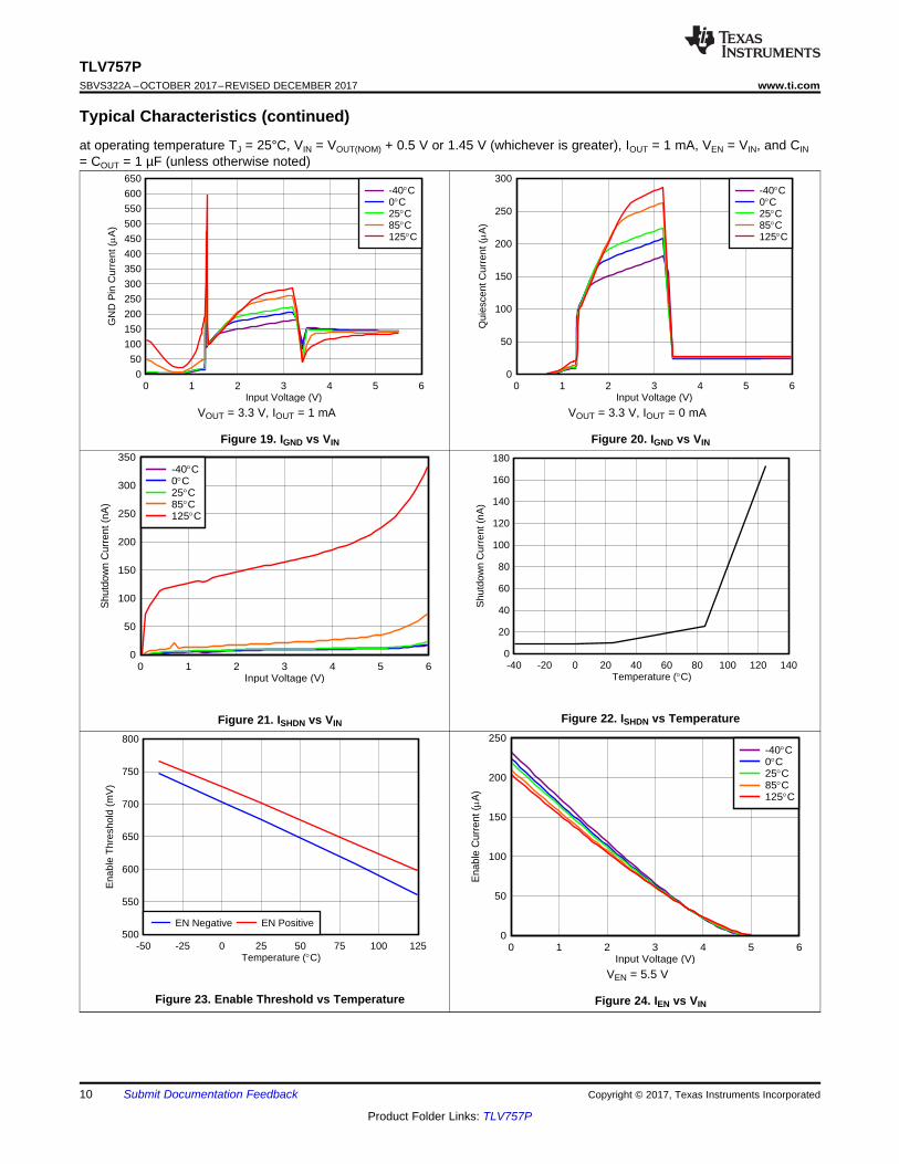
Typical Characteristics (continued)at operating temperature TJ = 25°C, VIN = VOUT(NOM) + 0.5 V or 1.45 V (whichever is greater), IOUT = 1 mA, VEN = VIN, and CIN= COUT = 1 µF (unless otherwise noted)
VOUT = 3.3 V, IOUT = 1 mA
Figure 19. IGND vs VIN
VOUT = 3.3 V, IOUT = 0 mA
Figure 20. IGND vs VIN
Figure 21. ISHDN vs VIN Figure 22. ISHDN vs Temperature
Figure 23. Enable Threshold vs Temperature
VEN = 5.5 V
Figure 24. IEN vs VIN

Output Current (mA)
Out
put V
olta
ge (
V)
0 200 400 600 800 1000 1200 1400 1600 1800 20000
0.8
1.6
2.4
3.2
4
-40qC0qC25qC85qC125qC
Output Current (mA)
Out
put V
olta
ge (
mV
)
0 1 2 3 4 50
50
100
150
200
250
300
350
400
450
500
550
600-40qC0qC25qC
85qC125qC
Temperature (qC)
UV
LO T
hres
hold
(V
)
-50 -25 0 25 50 75 100 1251.2
1.24
1.28
1.32
1.36
1.4
UVLO Negative UVLO Positive
11
TLV757Pwww.ti.com SBVS322A –OCTOBER 2017–REVISED DECEMBER 2017
Product Folder Links: TLV757P
Submit Documentation FeedbackCopyright © 2017, Texas Instruments Incorporated
Typical Characteristics (continued)at operating temperature TJ = 25°C, VIN = VOUT(NOM) + 0.5 V or 1.45 V (whichever is greater), IOUT = 1 mA, VEN = VIN, and CIN= COUT = 1 µF (unless otherwise noted)
Figure 25. UVLO Threshold vs Temperature Figure 26. IOUT vs VOUT Pulldown Resistor
Figure 27. 3.3-V Foldback Current Limit vs IOUT

t =120 · R
L
120 + RL
· COUT
+±
Bandgap
ThermalShutdown
UVLO
Logic
CurrentLimit
120 ��
IN
EN GND
OUT
R1
R2
12
TLV757PSBVS322A –OCTOBER 2017–REVISED DECEMBER 2017 www.ti.com
Product Folder Links: TLV757P
Submit Documentation Feedback Copyright © 2017, Texas Instruments Incorporated
7 Detailed Description
7.1 OverviewThe TLV757P belongs to a family of next-generation, low-dropout regulators (LDOs). This device consumes lowquiescent current and delivers excellent line and load transient performance. The TLV757P is optimized for widevariety of applications by supporting an input voltage range from 1.4 V to 5.5 V. To minimize cost and solutionsize, the device is offered in fixed output voltages ranging from 0.6 V to 5 V to support the lower core voltages ofmodern microcontrollers (MCUs).
This regulator offers foldback current limit, shutdown, and thermal protection. The operating junction temperatureis –40°C to +125°C.
7.2 Functional Block Diagram
(1) R2 = 550 kΩ, R1 = adjustable.
7.3 Feature Description
7.3.1 Undervoltage Lockout (UVLO)An undervoltage lockout (UVLO) circuit disables the output until the input voltage is greater than the rising UVLOvoltage (VUVLO). This circuit ensures that the device does not exhibit any unpredictable behavior when the supplyvoltage is lower than the operational range of the internal circuitry. When VIN is less than VUVLO, the output isconnected to ground with a 120-Ω pulldown resistor.
7.3.2 Enable (EN)The enable pin (EN) is active high. Enable the device by forcing the EN pin to exceed VHI. Turn off the device byforcing the EN pin below VLO. If shutdown capability is not required, connect EN to IN.
The device has an internal pull-down that connects a 120-Ω resistor to ground when the device is disabled. Thedischarge time after disabling depends on the output capacitance (COUT) and the load resistance (RL) in parallelwith the 120-Ω pulldown resistor. Equation 1 calculates the time constant τ:
(1)

13
TLV757Pwww.ti.com SBVS322A –OCTOBER 2017–REVISED DECEMBER 2017
Product Folder Links: TLV757P
Submit Documentation FeedbackCopyright © 2017, Texas Instruments Incorporated
Feature Description (continued)The EN pin is independent of the input pin, but if the EN pin is driven to a higher voltage than VIN, the currentinto the EN pin increases. This effect is illustrated in Figure 24. When the EN voltage is higher than the inputvoltage there is an increased current flow into the EN pin. If this increased flow causes problems in theapplication, sequence the EN pin after VIN is high, or to tie EN to VIN to prevent this flow increase fromhappening. If EN is driven to a higher voltage than VIN, limit the frequency on EN to below 10 kHz.
7.3.3 Internal Foldback Current LimitThe TLV757P has an internal current limit that protects the regulator during fault conditions. The current limit is ahybrid scheme with brick wall until the output voltage is less than 0.4 × VOUT(NOM). When the voltage drops below0.4 × VOUT(NOM), a foldback current limit is implemented which scales back the current as the output voltageapproaches GND. When the output shorts, the LDO supplies a typical current of ISC. The output voltage is notregulated when the device is in current limit. In this condition, the output voltage is the product of the regulatedcurrent and the load resistance. When the device output is shorts, the PMOS pass transistor dissipates power[(VIN – VOUT) × ISC] until thermal shutdown is triggered and the device turns off. After the device cools down, theinternal thermal shutdown circuit turns the device back on. If the fault condition continues, the device cyclesbetween current limit and thermal shutdown.
The foldback current-limit circuit limits the current that is allowed through the device to current levels lower thanthe minimum current limit at nominal VOUT current limit (ICL) during start up. See Figure 27 for typical current limitvalues. If the output is loaded by a constant-current load during start up, or if the output voltage is negative whenthe device is enabled, then the load current demanded by the load may exceed the foldback current limit and thedevice may not rise to the full output voltage. For constant-current loads, disable the output load until the outputhas risen to the nominal voltage.
Excess inductance can cause the current limit to oscillate. Minimize the inductance to keep the current limit fromoscillating during a fault condition.
7.3.4 Thermal ShutdownThermal shutdown protection disables the output when the junction temperature rises to approximately 165°C.Disabling the device eliminates the power dissipated by the device, allowing the device to cool. When thejunction temperature cools to approximately 155°C, the output circuitry is enabled again. Depending on powerdissipation, thermal resistance, and ambient temperature, the thermal protection circuit may cycle on and off.This cycling limits regulator dissipation which protects the circuit from damage as a result of overheating.
Activating the thermal shutdown feature usually indicates excessive power dissipation as a result of the productof the (VIN – VOUT) voltage and the load current. For reliable operation, limit junction temperature to a maximumof 125°C. To estimate the margin of safety in a complete design, increase the ambient temperature until thethermal protection is triggered; use worst-case loads and signal conditions.
The internal protection circuitry protects against overload conditions but is not intended to be activated in normaloperation. Continuously running the device into thermal shutdown degrades device reliability.

14
TLV757PSBVS322A –OCTOBER 2017–REVISED DECEMBER 2017 www.ti.com
Product Folder Links: TLV757P
Submit Documentation Feedback Copyright © 2017, Texas Instruments Incorporated
(1) All table conditions must be met.(2) The device is disabled when any condition is met.
7.4 Device Functional ModesTable 1 lists a comparison between the normal, dropout, and disabled modes of operation.
Table 1. Device Functional Modes Comparison
OPERATING MODEPARAMETER
VIN EN IOUT TJ
Normal (1) VIN > VOUT(NOM) + VDO VEN > VHI IOUT < ICL TJ < TSD
Dropout (1) VIN < VOUT(NOM) + VDO VEN > VHI — TJ < TSD
Disabled (2) VIN < VUVLO VEN < VLO — TJ > TSD
7.4.1 Normal OperationThe device regulates to the nominal output voltage when all of the following conditions are met.• The input voltage is greater than the nominal output voltage plus the dropout voltage (VOUT(NOM) + VDO)• The enable voltage has previously exceeded the enable rising threshold voltage and has not decreased
below the enable falling threshold• The output current is less than the current limit (IOUT < ICL)• The device junction temperature is less than the thermal shutdown temperature (TJ < TSD)
7.4.2 Dropout OperationIf the input voltage is lower than the nominal output voltage plus the specified dropout voltage, but all otherconditions are met for normal operation, the device operates in dropout. In this mode, the output voltage tracksthe input voltage. During this mode, the transient performance of the device degrades because the pass deviceis in a triode state and no longer controls the output voltage of the LDO. Line or load transients in dropout canresult in large output-voltage deviations.
When the device is in a steady dropout state (defined as when the device is in dropout, VIN < VOUT(NOM) + VDO,right after being in a normal regulation state, but not during startup), the pass-FET is driven as hard as possiblewhen the control loop is out of balance. During the normal time required for the device to regain regulation, VIN ≥VOUT(NOM) + VDO, VOUT can overshoot VOUT(NOM) during fast transients.
7.4.3 DisabledThe output is shut down by forcing the enable pin below VLO. When disabled, the pass device is turned off,internal circuits are shut down, and the output voltage is actively discharged to ground by an internal switch fromthe output to ground. The active pulldown is on when sufficient input voltage is provided.

15
TLV757Pwww.ti.com SBVS322A –OCTOBER 2017–REVISED DECEMBER 2017
Product Folder Links: TLV757P
Submit Documentation FeedbackCopyright © 2017, Texas Instruments Incorporated
8 Application and Implementation
NOTEInformation in the following applications sections is not part of the TI componentspecification, and TI does not warrant its accuracy or completeness. TI’s customers areresponsible for determining suitability of components for their purposes. Customers shouldvalidate and test their design implementation to confirm system functionality.
8.1 Application Information
8.1.1 Input and Output Capacitor SelectionThe TLV757P requires an output capacitance of 0.47 μF or larger for stability. Use X5R- and X7R-type ceramiccapacitors because these capacitors have minimal variation in capacitance value and equivalent seriesresistance (ESR) over temperature. When selecting a capacitor for a specific application, consider the DC biascharacteristics for the capacitor. Higher output voltages cause a significant derating of the capacitor. As ageneral rule, ceramic capacitors must be derated by 50%. For best performance, TI recommends a maximumoutput capacitance value of 200 µF.
Place a 1 µF or greater capacitor on the input pin of the LDO. Some input supplies have a high impedance.Placing a capacitor on the input supply reduces the input impedance. The input capacitor counteracts reactiveinput sources and improves transient response and PSRR. If the input supply has a high impedance over a largerange of frequencies, several input capacitors are used in parallel to lower the impedance over frequency. Use ahigher-value capacitor if large, fast, rise-time load transients are expected, or if the device is located severalinches from the input power source.
8.1.2 Dropout VoltageThe TLV757P uses a PMOS pass transistor to achieve low dropout. When (VIN – VOUT) is less than the dropoutvoltage (VDO), the PMOS pass device is in the linear region of operation and the input-to-output resistance is theRDS(ON) of the PMOS pass element. VDO scales linearly with the output current because the PMOS devicefunctions like a resistor in dropout mode. As with any linear regulator, PSRR and transient response degrade as(VIN – VOUT) approaches dropout operation. See Figure 14 and Figure 15 for typical dropout values.
8.1.3 Exiting DropoutSome applications have transients that place the LDO into dropout, such as slower ramps on VIN during start-up.As with other LDOs, the output may overshoot on recovery from these conditions. A ramping input supply causesan LDO to overshoot on start-up when the slew rate and voltage levels are in the correct range; see Figure 28.Use an enable signal to avoid this condition.

Input Voltage
Output Voltage
Output Voltage in normal regulation.
Dropout VOUT = VIN - VDO
VIN = VOUT(nom) + VDO
Response time for LDO to get back into
regulation. Load current discharges output voltage.
Vol
tage
Time
16
TLV757PSBVS322A –OCTOBER 2017–REVISED DECEMBER 2017 www.ti.com
Product Folder Links: TLV757P
Submit Documentation Feedback Copyright © 2017, Texas Instruments Incorporated
Application Information (continued)
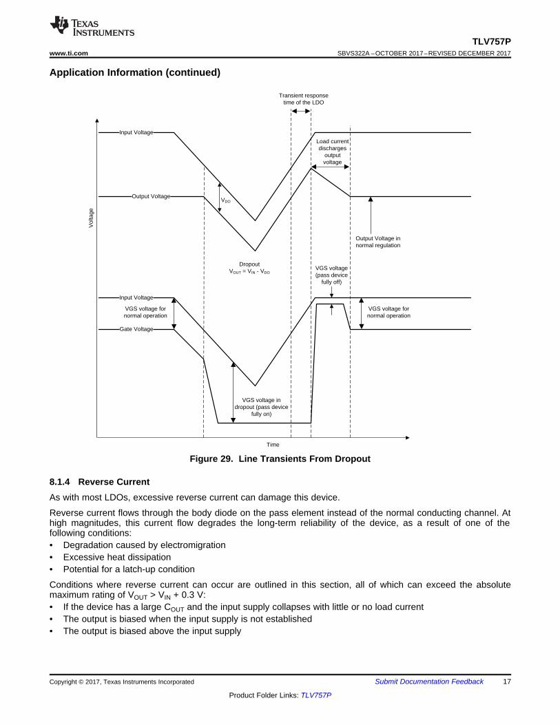
Figure 28. Startup into Dropout
Line transients out of dropout can also cause overshoot on the output of the regulator. These overshoots arecaused by the error amplifier having to drive the gate capacitance of the pass element and bring the gate back tothe correct voltage for proper regulation. Figure 29 illustrates what is happening internally with the gate voltageand how overshoot can be caused during operation. When the LDO is placed in dropout, the gate voltage (VGS)is pulled all the way down to give the pass device the lowest on-resistance as possible. However, if a linetransient occurs while the device is in dropout, the loop is not in regulation which can cause the output toovershoot until the loop responds and the output current pulls the output voltage back down into regulation. Ifthese transients are not acceptable, then continue to add input capacitance in the system until the transient isslow enough to reduce the overshoot.
Output Voltage in normal regulation
Dropout VOUT = VIN - VDO
Transient response time of the LDO
Load current discharges
output voltage
Vol
tage
Time
VGS voltage for normal operation
VGS voltage in dropout (pass device
fully on)
VDO
Gate Voltage
Input Voltage
VGS voltage for normal operation
Input Voltage
Output Voltage
VGS voltage (pass device
fully off)
17
TLV757Pwww.ti.com SBVS322A –OCTOBER 2017–REVISED DECEMBER 2017
Product Folder Links: TLV757P
Submit Documentation FeedbackCopyright © 2017, Texas Instruments Incorporated
Application Information (continued)
Figure 29. Line Transients From Dropout
8.1.4 Reverse CurrentAs with most LDOs, excessive reverse current can damage this device.
Reverse current flows through the body diode on the pass element instead of the normal conducting channel. Athigh magnitudes, this current flow degrades the long-term reliability of the device, as a result of one of thefollowing conditions:• Degradation caused by electromigration• Excessive heat dissipation• Potential for a latch-up condition
Conditions where reverse current can occur are outlined in this section, all of which can exceed the absolutemaximum rating of VOUT > VIN + 0.3 V:• If the device has a large COUT and the input supply collapses with little or no load current• The output is biased when the input supply is not established• The output is biased above the input supply

Device
IN OUT
GND
COUT
CIN
Schottky Diode
Internal Body Diode
18
TLV757PSBVS322A –OCTOBER 2017–REVISED DECEMBER 2017 www.ti.com
Product Folder Links: TLV757P
Submit Documentation Feedback Copyright © 2017, Texas Instruments Incorporated
Application Information (continued)If reverse current flow is expected in the application, external protection must be used to protect the device.Figure 30 shows one approach of protecting the device.
Figure 30. Example Circuit for Reverse Current Protection Using a Schottky Diode
8.1.5 Power Dissipation (PD)Circuit reliability demands that proper consideration is given to device power dissipation, location of the circuit onthe printed circuit board (PCB), and correct sizing of the thermal plane. The PCB area around the regulator mustbe as free of other heat-generating devices as possible that cause added thermal stresses.
As a first-order approximation, power dissipation in the regulator depends on the input-to-output voltagedifference and load conditions. Use Equation 2 to approximate PD:
PD = (VIN – VOUT) × IOUT (2)
It is important to minimize power dissipation to achieve greater efficiency. This minimizing process is achieved byselecting the correct system voltage rails. Proper selection helps obtain the minimum input-to-output voltagedifferential . The low dropout of the device allows for maximum efficiency across a wide range of output voltages.
The main heat conduction path for the device is through the thermal pad on the package. As such, the thermalpad must be soldered to a copper pad area under the device. This pad area should contain an array of platedvias that conduct heat to inner plane areas or to a bottom-side copper plane.
The maximum allowable junction temperature (TJ) determines the maximum power dissipation for the device.Power dissipation and junction temperature are most often related by the junction-to-ambient thermal resistance(θJA) of the combined PCB, device package, and the temperature of the ambient air (TA), according toEquation 3.
TJ = TA + θJA × PD (3)
Unfortunately, this thermal resistance (θJA) is dependent on the heat-spreading capability built into the particularPCB design, and therefore varies according to the total copper area, copper weight, and location of the planes.The θJA value is only used as a relative measure of package thermal performance. θJA is the sum of the VQFNpackage junction-to-case (bottom) thermal resistance (θJCbot) plus the thermal resistance contribution by the PCBcopper.

DC-DCConverter TLV757P
IN
EN
OUT
GND
1 �F1 �F
OFF
ON
Load
Copyright © 2017, Texas Instruments Incorporated
Y
Y Y ´
JT J T JT D: T = T + PY ´
JB J B JB D: T = T + P
19
TLV757Pwww.ti.com SBVS322A –OCTOBER 2017–REVISED DECEMBER 2017
Product Folder Links: TLV757P
Submit Documentation FeedbackCopyright © 2017, Texas Instruments Incorporated
Application Information (continued)8.1.5.1 Estimating Junction TemperatureThe JEDEC standard recommends the use of psi (Ψ) thermal metrics to estimate the junction temperatures ofthe LDO when in-circuit on a typical PCB board application. These metrics are not thermal resistances, but offerpractical and relative means of estimating junction temperatures. These psi metrics are independent of thecopper-spreading area. The key thermal metrics (ΨJT and ΨJB) are shown in the table and are used inaccordance with Equation 4.
where:• PD is the power dissipated as shown in Equation 2• TT is the temperature at the center-top of the device package, and• TB is the PCB surface temperature measured 1 mm from the device package and centered on the package
edge (4)
8.2 Typical Application
Figure 31. TLV757P Typical Application
8.2.1 Design RequirementsTable 2 lists the design requirements for this application.
Table 2. Design ParametersPARAMETER DESIGN REQUIREMENTInput voltage 2.5 V
Output voltage 1.8 VInput current 700 mA (maximum)Output load 600-mA DC
Maximum ambient temperature 70°C

Time (ms)
Vol
tage
(V
)
Inpu
t Cur
rent
(A
)
0 0.5 1 1.5 2 2.5 3 3.5 4 4.5 50 0
0.5 0.2
1 0.4
1.5 0.6
2 0.8
2.5 1
3 1.2
VINVOUTENIIN
Frequency (Hz)
Pow
er S
uppl
y R
ejec
tion
Rat
io (
dB)
0
20
40
60
80
100
10 100 1k 10k 100k 1M 10M
IOUT = 600 mA
I =OUT(t)
COUT OUT´ dV (t)
dt
VOUT(t)
RLOAD
+
20
TLV757PSBVS322A –OCTOBER 2017–REVISED DECEMBER 2017 www.ti.com
Product Folder Links: TLV757P
Submit Documentation Feedback Copyright © 2017, Texas Instruments Incorporated
8.2.2 Detailed Design Procedure
8.2.2.1 Input CurrentDuring normal operation, the input current to the LDO is approximately equal to the output current of the LDO.During startup, the input current is higher as a result of the inrush current charging the output capacitor. UseEquation 5 to calculate the current through the input.
where:• VOUT(t) is the instantaneous output voltage of the turn-on ramp• dVOUT(t) / dt is the slope of the VOUT ramp• RLOAD is the resistive load impedance (5)
8.2.2.2 Thermal DissipationThe junction temperature can be determined using the junction-to-ambient thermal resistance (RθJA) and the totalpower dissipation (PD). Use Equation 6 to calculate the power dissipation. Multiply PD by RθJA and add theambient temperature (TA) to calculate the junction temperature (TJ) as Equation 7 shows.
PD = (IGND+ IOUT) × (VIN – VOUT) (6)TJ = RθJA × PD + TA (7)
If the (TJ(MAX)) value does not exceed 125°C calculate the maximum ambient temperature as Equation 8 shows.Equation 9 calculates the maximum ambient temperature with a value of 82.916°C.
TA(MAX) = TJ(MAX) – RθJA × PD (8)TA(MAX) = 125°C – 100.2 × (2.5 V –1.8 V) × (0.6 A) = 82.916°C (9)
8.2.3 Application Curves
Figure 32. Startup With a 600-mA Load
VIN = 2.5 V, VOUT = 1.8 V, IOUT = 600 mA
Figure 33. PSRR (2.5 V to 1.8 V at 600 mA)
9 Power Supply RecommendationsConnect a low output impedance power supply directly to the IN pin of the TLV757P. If the input source isreactive, consider using multiple input capacitors in parallel with the 1-µF input capacitor to lower the input supplyimpedance over frequency.

VINVOUT
GND PLANE
Represents via used for application specific connections
1
2
3 4
6
CINCOUT
EN
5
VOUTVIN
GND PLANE
Represents via used for application specific connections
1
2
3 4
5
COUTCIN
EN
21
TLV757Pwww.ti.com SBVS322A –OCTOBER 2017–REVISED DECEMBER 2017
Product Folder Links: TLV757P
Submit Documentation FeedbackCopyright © 2017, Texas Instruments Incorporated
10 Layout
10.1 Layout Guidelines• Place input and output capacitors as close as possible to the device.• Use copper planes for device connections to optimize thermal performance.• Place thermal vias around the device to distribute the heat.
10.2 Layout Examples
Figure 34. Layout Example: DBV Package
Figure 35. Layout Example: DRV Package

22
TLV757PSBVS322A –OCTOBER 2017–REVISED DECEMBER 2017 www.ti.com
Product Folder Links: TLV757P
Submit Documentation Feedback Copyright © 2017, Texas Instruments Incorporated
(1) For the most current package and ordering information see the Package Option Addendum at the end of this document, or visit thedevice product folder on www.ti.com.
(2) Output voltages from 0.6 V to 5 V in 50-mV increments are available. Contact the factory for details and availability.
11 Device and Documentation Support
11.1 Device Support
11.1.1 Device Nomenclature
Table 3. Device Nomenclature (1) (2)
PRODUCT VOUT
TLV757xx(x)Pyyyz
xx(x) is the nominal output voltage. For output voltages with a resolution of 50 mV, two digits are usedin the ordering number; otherwise, three digits are used (for example, 28 = 2.8 V; 125 = 1.25 V).P indicates an active output discharge feature. All members of the TLV757P family will activelydischarge the output when the device is disabled.yyy is the package designator.z is the package quantity. R is for reel (3000 pieces), T is for tape (250 pieces).
11.2 Receiving Notification of Documentation UpdatesTo receive notification of documentation updates, navigate to the device product folder on ti.com. In the upperright corner, click on Alert me to register and receive a weekly digest of any product information that haschanged. For change details, review the revision history included in any revised document.
11.3 Community ResourcesThe following links connect to TI community resources. Linked contents are provided "AS IS" by the respectivecontributors. They do not constitute TI specifications and do not necessarily reflect TI's views; see TI's Terms ofUse.
TI E2E™ Online Community TI's Engineer-to-Engineer (E2E) Community. Created to foster collaborationamong engineers. At e2e.ti.com, you can ask questions, share knowledge, explore ideas and helpsolve problems with fellow engineers.
Design Support TI's Design Support Quickly find helpful E2E forums along with design support tools andcontact information for technical support.
11.4 TrademarksE2E is a trademark of Texas Instruments.All other trademarks are the property of their respective owners.
11.5 Electrostatic Discharge CautionThis integrated circuit can be damaged by ESD. Texas Instruments recommends that all integrated circuits be handled withappropriate precautions. Failure to observe proper handling and installation procedures can cause damage.
ESD damage can range from subtle performance degradation to complete device failure. Precision integrated circuits may be moresusceptible to damage because very small parametric changes could cause the device not to meet its published specifications.
11.6 GlossarySLYZ022 — TI Glossary.
This glossary lists and explains terms, acronyms, and definitions.
12 Mechanical, Packaging, and Orderable InformationThe following pages include mechanical, packaging, and orderable information. This information is the mostcurrent data available for the designated devices. This data is subject to change without notice and revision ofthis document. For browser-based versions of this data sheet, refer to the left-hand navigation.

PACKAGE OPTION ADDENDUM
www.ti.com 10-Dec-2020
Addendum-Page 1
PACKAGING INFORMATION
Orderable Device Status(1)
Package Type PackageDrawing
Pins PackageQty
Eco Plan(2)
Lead finish/Ball material
(6)
MSL Peak Temp(3)
Op Temp (°C) Device Marking(4/5)
Samples
TLV75709PDBVR ACTIVE SOT-23 DBV 5 3000 RoHS & Green NIPDAU | SN Level-1-260C-UNLIM -40 to 125 1H8F
TLV75709PDRVR ACTIVE WSON DRV 6 3000 RoHS & Green NIPDAU Level-1-260C-UNLIM -40 to 125 1HGH
TLV75710PDBVR ACTIVE SOT-23 DBV 5 3000 RoHS & Green NIPDAU | SN Level-1-260C-UNLIM -40 to 125 1FEF
TLV75710PDRVR ACTIVE WSON DRV 6 3000 RoHS & Green NIPDAU Level-1-260C-UNLIM -40 to 125 1HHH
TLV75712PDBVR ACTIVE SOT-23 DBV 5 3000 RoHS & Green NIPDAU | SN Level-1-260C-UNLIM -40 to 125 1FFF
TLV75712PDRVR ACTIVE WSON DRV 6 3000 RoHS & Green NIPDAU Level-1-260C-UNLIM -40 to 125 1HIH
TLV75715PDBVR ACTIVE SOT-23 DBV 5 3000 RoHS & Green NIPDAU | SN Level-1-260C-UNLIM -40 to 125 1FGF
TLV75715PDRVR ACTIVE WSON DRV 6 3000 RoHS & Green NIPDAU Level-1-260C-UNLIM -40 to 125 1HJH
TLV75718PDBVR ACTIVE SOT-23 DBV 5 3000 RoHS & Green NIPDAU | SN Level-1-260C-UNLIM -40 to 125 1FHF
TLV75718PDRVR ACTIVE WSON DRV 6 3000 RoHS & Green NIPDAU Level-1-260C-UNLIM -40 to 125 1HKH
TLV75719PDBVR ACTIVE SOT-23 DBV 5 3000 RoHS & Green NIPDAU | SN Level-1-260C-UNLIM -40 to 125 1H7F
TLV75719PDRVR ACTIVE WSON DRV 6 3000 RoHS & Green NIPDAU Level-1-260C-UNLIM -40 to 125 1HLH
TLV75725PDBVR ACTIVE SOT-23 DBV 5 3000 RoHS & Green NIPDAU | SN Level-1-260C-UNLIM -40 to 125 1FIF
TLV75725PDRVR ACTIVE WSON DRV 6 3000 RoHS & Green NIPDAU Level-1-260C-UNLIM -40 to 125 1HMH
TLV75728PDBVR ACTIVE SOT-23 DBV 5 3000 RoHS & Green NIPDAU | SN Level-1-260C-UNLIM -40 to 125 1FJF
TLV75728PDRVR ACTIVE WSON DRV 6 3000 RoHS & Green NIPDAU Level-1-260C-UNLIM -40 to 125 1HNH
TLV75729PDBVR ACTIVE SOT-23 DBV 5 3000 RoHS & Green NIPDAU | SN Level-1-260C-UNLIM -40 to 125 1H9F
TLV75730PDBVR ACTIVE SOT-23 DBV 5 3000 RoHS & Green NIPDAU | SN Level-1-260C-UNLIM -40 to 125 1GHF
TLV75730PDRVR ACTIVE WSON DRV 6 3000 RoHS & Green NIPDAU Level-1-260C-UNLIM -40 to 125 1HOH
TLV75733PDBVR ACTIVE SOT-23 DBV 5 3000 RoHS & Green NIPDAU | SN Level-1-260C-UNLIM -40 to 125 1FKF

PACKAGE OPTION ADDENDUM
www.ti.com 10-Dec-2020
Addendum-Page 2
Orderable Device Status(1)
Package Type PackageDrawing
Pins PackageQty
Eco Plan(2)
Lead finish/Ball material
(6)
MSL Peak Temp(3)
Op Temp (°C) Device Marking(4/5)
Samples
TLV75733PDRVR ACTIVE WSON DRV 6 3000 RoHS & Green NIPDAU Level-1-260C-UNLIM -40 to 125 1HPH
TLV75740PDRVR ACTIVE WSON DRV 6 3000 RoHS & Green NIPDAU Level-1-260C-UNLIM -40 to 125 1HQH
(1) The marketing status values are defined as follows:ACTIVE: Product device recommended for new designs.LIFEBUY: TI has announced that the device will be discontinued, and a lifetime-buy period is in effect.NRND: Not recommended for new designs. Device is in production to support existing customers, but TI does not recommend using this part in a new design.PREVIEW: Device has been announced but is not in production. Samples may or may not be available.OBSOLETE: TI has discontinued the production of the device.
(2) RoHS: TI defines "RoHS" to mean semiconductor products that are compliant with the current EU RoHS requirements for all 10 RoHS substances, including the requirement that RoHS substancedo not exceed 0.1% by weight in homogeneous materials. Where designed to be soldered at high temperatures, "RoHS" products are suitable for use in specified lead-free processes. TI mayreference these types of products as "Pb-Free".RoHS Exempt: TI defines "RoHS Exempt" to mean products that contain lead but are compliant with EU RoHS pursuant to a specific EU RoHS exemption.Green: TI defines "Green" to mean the content of Chlorine (Cl) and Bromine (Br) based flame retardants meet JS709B low halogen requirements of <=1000ppm threshold. Antimony trioxide basedflame retardants must also meet the <=1000ppm threshold requirement.
(3) MSL, Peak Temp. - The Moisture Sensitivity Level rating according to the JEDEC industry standard classifications, and peak solder temperature.
(4) There may be additional marking, which relates to the logo, the lot trace code information, or the environmental category on the device.
(5) Multiple Device Markings will be inside parentheses. Only one Device Marking contained in parentheses and separated by a "~" will appear on a device. If a line is indented then it is a continuationof the previous line and the two combined represent the entire Device Marking for that device.
(6) Lead finish/Ball material - Orderable Devices may have multiple material finish options. Finish options are separated by a vertical ruled line. Lead finish/Ball material values may wrap to twolines if the finish value exceeds the maximum column width.
Important Information and Disclaimer:The information provided on this page represents TI's knowledge and belief as of the date that it is provided. TI bases its knowledge and belief on informationprovided by third parties, and makes no representation or warranty as to the accuracy of such information. Efforts are underway to better integrate information from third parties. TI has taken andcontinues to take reasonable steps to provide representative and accurate information but may not have conducted destructive testing or chemical analysis on incoming materials and chemicals.TI and TI suppliers consider certain information to be proprietary, and thus CAS numbers and other limited information may not be available for release.
In no event shall TI's liability arising out of such information exceed the total purchase price of the TI part(s) at issue in this document sold by TI to Customer on an annual basis.

TAPE AND REEL INFORMATION
*All dimensions are nominal
Device PackageType
PackageDrawing
Pins SPQ ReelDiameter
(mm)
ReelWidth
W1 (mm)
A0(mm)
B0(mm)
K0(mm)
P1(mm)
W(mm)
Pin1Quadrant
TLV75709PDBVR SOT-23 DBV 5 3000 180.0 8.4 3.2 3.2 1.4 4.0 8.0 Q3
TLV75709PDRVR WSON DRV 6 3000 180.0 8.4 2.3 2.3 1.15 4.0 8.0 Q2
TLV75710PDBVR SOT-23 DBV 5 3000 178.0 9.0 3.3 3.2 1.4 4.0 8.0 Q3
TLV75710PDBVR SOT-23 DBV 5 3000 180.0 8.4 3.2 3.2 1.4 4.0 8.0 Q3
TLV75710PDRVR WSON DRV 6 3000 180.0 8.4 2.3 2.3 1.15 4.0 8.0 Q2
TLV75712PDBVR SOT-23 DBV 5 3000 178.0 9.0 3.3 3.2 1.4 4.0 8.0 Q3
TLV75712PDBVR SOT-23 DBV 5 3000 180.0 8.4 3.2 3.2 1.4 4.0 8.0 Q3
TLV75712PDRVR WSON DRV 6 3000 180.0 8.4 2.3 2.3 1.15 4.0 8.0 Q2
TLV75715PDBVR SOT-23 DBV 5 3000 180.0 8.4 3.2 3.2 1.4 4.0 8.0 Q3
TLV75715PDBVR SOT-23 DBV 5 3000 178.0 9.0 3.3 3.2 1.4 4.0 8.0 Q3
TLV75715PDRVR WSON DRV 6 3000 180.0 8.4 2.3 2.3 1.15 4.0 8.0 Q2
TLV75718PDBVR SOT-23 DBV 5 3000 180.0 8.4 3.2 3.2 1.4 4.0 8.0 Q3
TLV75718PDRVR WSON DRV 6 3000 180.0 8.4 2.3 2.3 1.15 4.0 8.0 Q2
TLV75719PDBVR SOT-23 DBV 5 3000 180.0 8.4 3.2 3.2 1.4 4.0 8.0 Q3
TLV75719PDBVR SOT-23 DBV 5 3000 178.0 9.0 3.3 3.2 1.4 4.0 8.0 Q3
TLV75719PDRVR WSON DRV 6 3000 180.0 8.4 2.3 2.3 1.15 4.0 8.0 Q2
TLV75725PDBVR SOT-23 DBV 5 3000 178.0 9.0 3.3 3.2 1.4 4.0 8.0 Q3
TLV75725PDBVR SOT-23 DBV 5 3000 180.0 8.4 3.2 3.2 1.4 4.0 8.0 Q3
PACKAGE MATERIALS INFORMATION
www.ti.com 16-Feb-2019
Pack Materials-Page 1
Device PackageType
PackageDrawing
Pins SPQ ReelDiameter
(mm)
ReelWidth
W1 (mm)
A0(mm)
B0(mm)
K0(mm)
P1(mm)
W(mm)
Pin1Quadrant
TLV75725PDRVR WSON DRV 6 3000 180.0 8.4 2.3 2.3 1.15 4.0 8.0 Q2
TLV75728PDBVR SOT-23 DBV 5 3000 180.0 8.4 3.2 3.2 1.4 4.0 8.0 Q3
TLV75728PDBVR SOT-23 DBV 5 3000 178.0 9.0 3.3 3.2 1.4 4.0 8.0 Q3
TLV75728PDRVR WSON DRV 6 3000 180.0 8.4 2.3 2.3 1.15 4.0 8.0 Q2
TLV75729PDBVR SOT-23 DBV 5 3000 180.0 8.4 3.2 3.2 1.4 4.0 8.0 Q3
TLV75729PDBVR SOT-23 DBV 5 3000 178.0 9.0 3.3 3.2 1.4 4.0 8.0 Q3
TLV75730PDBVR SOT-23 DBV 5 3000 180.0 8.4 3.2 3.2 1.4 4.0 8.0 Q3
TLV75730PDBVR SOT-23 DBV 5 3000 178.0 9.0 3.3 3.2 1.4 4.0 8.0 Q3
TLV75730PDRVR WSON DRV 6 3000 180.0 8.4 2.3 2.3 1.15 4.0 8.0 Q2
TLV75733PDBVR SOT-23 DBV 5 3000 178.0 9.0 3.3 3.2 1.4 4.0 8.0 Q3
TLV75733PDBVR SOT-23 DBV 5 3000 180.0 8.4 3.2 3.2 1.4 4.0 8.0 Q3
TLV75733PDRVR WSON DRV 6 3000 180.0 8.4 2.3 2.3 1.15 4.0 8.0 Q2
TLV75740PDRVR WSON DRV 6 3000 180.0 8.4 2.3 2.3 1.15 4.0 8.0 Q2
*All dimensions are nominal
Device Package Type Package Drawing Pins SPQ Length (mm) Width (mm) Height (mm)
TLV75709PDBVR SOT-23 DBV 5 3000 210.0 185.0 35.0
TLV75709PDRVR WSON DRV 6 3000 210.0 185.0 35.0
TLV75710PDBVR SOT-23 DBV 5 3000 180.0 180.0 18.0
TLV75710PDBVR SOT-23 DBV 5 3000 210.0 185.0 35.0
PACKAGE MATERIALS INFORMATION
www.ti.com 16-Feb-2019
Pack Materials-Page 2

Device Package Type Package Drawing Pins SPQ Length (mm) Width (mm) Height (mm)
TLV75710PDRVR WSON DRV 6 3000 210.0 185.0 35.0
TLV75712PDBVR SOT-23 DBV 5 3000 180.0 180.0 18.0
TLV75712PDBVR SOT-23 DBV 5 3000 210.0 185.0 35.0
TLV75712PDRVR WSON DRV 6 3000 210.0 185.0 35.0
TLV75715PDBVR SOT-23 DBV 5 3000 210.0 185.0 35.0
TLV75715PDBVR SOT-23 DBV 5 3000 180.0 180.0 18.0
TLV75715PDRVR WSON DRV 6 3000 210.0 185.0 35.0
TLV75718PDBVR SOT-23 DBV 5 3000 210.0 185.0 35.0
TLV75718PDRVR WSON DRV 6 3000 210.0 185.0 35.0
TLV75719PDBVR SOT-23 DBV 5 3000 210.0 185.0 35.0
TLV75719PDBVR SOT-23 DBV 5 3000 180.0 180.0 18.0
TLV75719PDRVR WSON DRV 6 3000 210.0 185.0 35.0
TLV75725PDBVR SOT-23 DBV 5 3000 180.0 180.0 18.0
TLV75725PDBVR SOT-23 DBV 5 3000 210.0 185.0 35.0
TLV75725PDRVR WSON DRV 6 3000 210.0 185.0 35.0
TLV75728PDBVR SOT-23 DBV 5 3000 210.0 185.0 35.0
TLV75728PDBVR SOT-23 DBV 5 3000 180.0 180.0 18.0
TLV75728PDRVR WSON DRV 6 3000 210.0 185.0 35.0
TLV75729PDBVR SOT-23 DBV 5 3000 210.0 185.0 35.0
TLV75729PDBVR SOT-23 DBV 5 3000 180.0 180.0 18.0
TLV75730PDBVR SOT-23 DBV 5 3000 210.0 185.0 35.0
TLV75730PDBVR SOT-23 DBV 5 3000 180.0 180.0 18.0
TLV75730PDRVR WSON DRV 6 3000 210.0 185.0 35.0
TLV75733PDBVR SOT-23 DBV 5 3000 180.0 180.0 18.0
TLV75733PDBVR SOT-23 DBV 5 3000 210.0 185.0 35.0
TLV75733PDRVR WSON DRV 6 3000 210.0 185.0 35.0
TLV75740PDRVR WSON DRV 6 3000 210.0 185.0 35.0
PACKAGE MATERIALS INFORMATION
www.ti.com 16-Feb-2019
Pack Materials-Page 3

www.ti.com
PACKAGE OUTLINE
C
0.220.08 TYP
0.25
3.02.6
2X 0.95
1.9
1.450.90
0.150.00 TYP
5X 0.50.3
0.60.3 TYP
80 TYP
1.9
A
3.052.75
B1.751.45
(1.1)
SOT-23 - 1.45 mm max heightDBV0005ASMALL OUTLINE TRANSISTOR
4214839/F 06/2021
NOTES: 1. All linear dimensions are in millimeters. Any dimensions in parenthesis are for reference only. Dimensioning and tolerancing per ASME Y14.5M.2. This drawing is subject to change without notice.3. Refernce JEDEC MO-178.4. Body dimensions do not include mold flash, protrusions, or gate burrs. Mold flash, protrusions, or gate burrs shall not exceed 0.25 mm per side.
0.2 C A B
1
34
5
2
INDEX AREAPIN 1
GAGE PLANE
SEATING PLANE
0.1 C
SCALE 4.000
www.ti.com
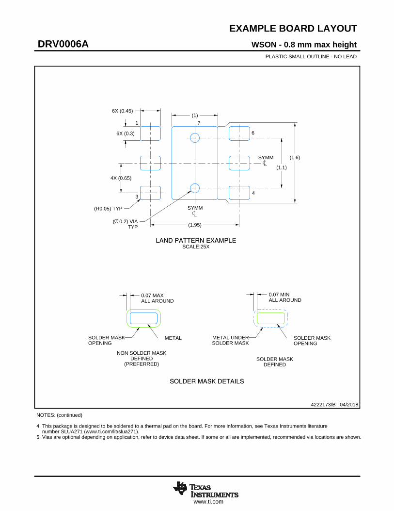
EXAMPLE BOARD LAYOUT
0.07 MAXARROUND
0.07 MINARROUND
5X (1.1)
5X (0.6)
(2.6)
(1.9)
2X (0.95)
(R0.05) TYP
4214839/F 06/2021
SOT-23 - 1.45 mm max heightDBV0005ASMALL OUTLINE TRANSISTOR
NOTES: (continued) 5. Publication IPC-7351 may have alternate designs. 6. Solder mask tolerances between and around signal pads can vary based on board fabrication site.
SYMM
LAND PATTERN EXAMPLEEXPOSED METAL SHOWN
SCALE:15X
PKG
1
3 4
5
2
SOLDER MASKOPENINGMETAL UNDER
SOLDER MASK
SOLDER MASKDEFINED
EXPOSED METAL
METALSOLDER MASKOPENING
NON SOLDER MASKDEFINED
(PREFERRED)
SOLDER MASK DETAILS
EXPOSED METAL

www.ti.com
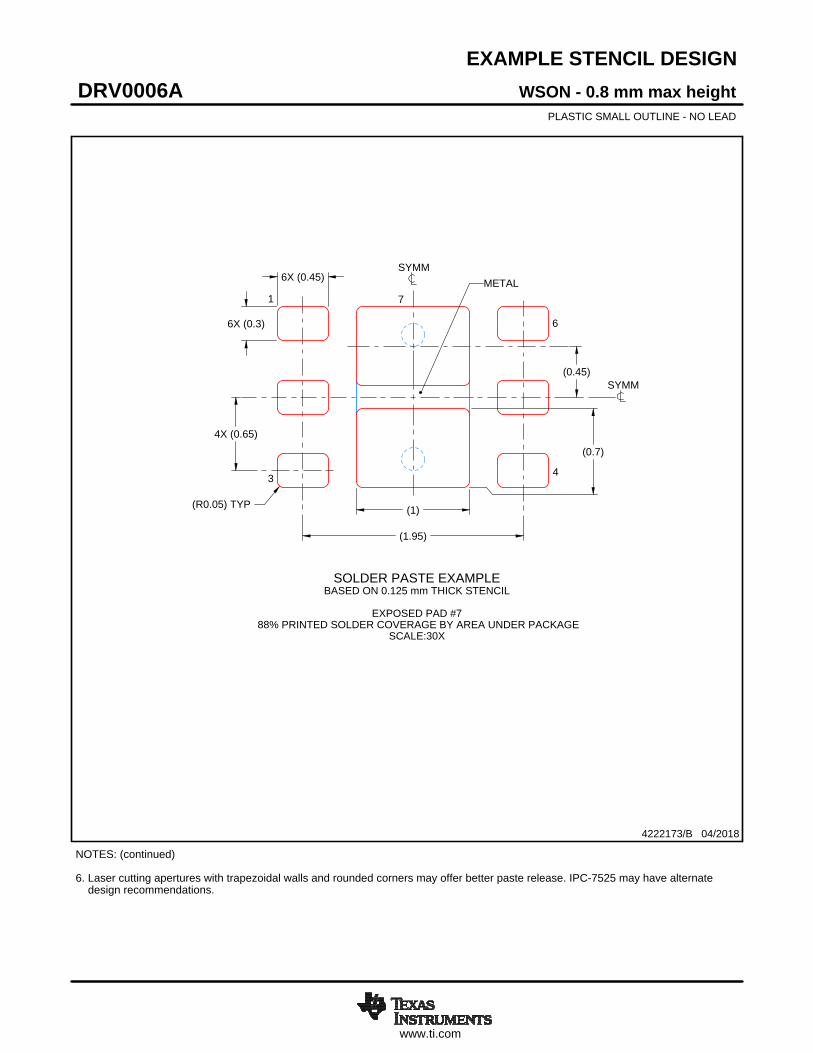
EXAMPLE STENCIL DESIGN
(2.6)
(1.9)
2X(0.95)
5X (1.1)
5X (0.6)
(R0.05) TYP
SOT-23 - 1.45 mm max heightDBV0005ASMALL OUTLINE TRANSISTOR
4214839/F 06/2021
NOTES: (continued) 7. Laser cutting apertures with trapezoidal walls and rounded corners may offer better paste release. IPC-7525 may have alternate design recommendations. 8. Board assembly site may have different recommendations for stencil design.
SOLDER PASTE EXAMPLEBASED ON 0.125 mm THICK STENCIL
SCALE:15X
SYMM
PKG
1
3 4
5
2

GENERIC PACKAGE VIEW
Images above are just a representation of the package family, actual package may vary.Refer to the product data sheet for package details.
DRV 6 WSON - 0.8 mm max heightPLASTIC SMALL OUTLINE - NO LEAD
4206925/F

www.ti.com
PACKAGE OUTLINE
C
6X 0.350.25
1.6 0.1
6X 0.30.2
2X1.3
1 0.1
4X 0.65
0.80.7
0.050.00
B 2.11.9
A
2.11.9
(0.2) TYP
WSON - 0.8 mm max heightDRV0006APLASTIC SMALL OUTLINE - NO LEAD
4222173/B 04/2018
PIN 1 INDEX AREA
SEATING PLANE
0.08 C
1
34
6
(OPTIONAL)PIN 1 ID
0.1 C A B0.05 C
THERMAL PADEXPOSED
7
NOTES: 1. All linear dimensions are in millimeters. Any dimensions in parenthesis are for reference only. Dimensioning and tolerancing per ASME Y14.5M. 2. This drawing is subject to change without notice. 3. The package thermal pad must be soldered to the printed circuit board for thermal and mechanical performance.
SCALE 5.500
www.ti.com
EXAMPLE BOARD LAYOUT
0.07 MINALL AROUND
0.07 MAXALL AROUND
(1)
4X (0.65)
(1.95)
6X (0.3)
6X (0.45)
(1.6)
(R0.05) TYP
( 0.2) VIATYP
(1.1)
WSON - 0.8 mm max heightDRV0006APLASTIC SMALL OUTLINE - NO LEAD
4222173/B 04/2018
SYMM
1
34
6
SYMM
LAND PATTERN EXAMPLESCALE:25X
7
NOTES: (continued) 4. This package is designed to be soldered to a thermal pad on the board. For more information, see Texas Instruments literature number SLUA271 (www.ti.com/lit/slua271).5. Vias are optional depending on application, refer to device data sheet. If some or all are implemented, recommended via locations are shown.
SOLDER MASKOPENINGSOLDER MASK
METAL UNDER
SOLDER MASKDEFINED
METALSOLDER MASKOPENING
SOLDER MASK DETAILS
NON SOLDER MASKDEFINED
(PREFERRED)
www.ti.com
EXAMPLE STENCIL DESIGN
6X (0.3)
6X (0.45)
4X (0.65)
(0.7)
(1)
(1.95)
(R0.05) TYP
(0.45)
WSON - 0.8 mm max heightDRV0006APLASTIC SMALL OUTLINE - NO LEAD
4222173/B 04/2018
NOTES: (continued) 6. Laser cutting apertures with trapezoidal walls and rounded corners may offer better paste release. IPC-7525 may have alternate design recommendations.
SOLDER PASTE EXAMPLEBASED ON 0.125 mm THICK STENCIL
EXPOSED PAD #7
88% PRINTED SOLDER COVERAGE BY AREA UNDER PACKAGESCALE:30X
SYMM
1
3 4
6
SYMM
METAL7
IMPORTANT NOTICE AND DISCLAIMERTI PROVIDES TECHNICAL AND RELIABILITY DATA (INCLUDING DATASHEETS), DESIGN RESOURCES (INCLUDING REFERENCEDESIGNS), APPLICATION OR OTHER DESIGN ADVICE, WEB TOOLS, SAFETY INFORMATION, AND OTHER RESOURCES “AS IS”AND WITH ALL FAULTS, AND DISCLAIMS ALL WARRANTIES, EXPRESS AND IMPLIED, INCLUDING WITHOUT LIMITATION ANYIMPLIED WARRANTIES OF MERCHANTABILITY, FITNESS FOR A PARTICULAR PURPOSE OR NON-INFRINGEMENT OF THIRDPARTY INTELLECTUAL PROPERTY RIGHTS.These resources are intended for skilled developers designing with TI products. You are solely responsible for (1) selecting the appropriateTI products for your application, (2) designing, validating and testing your application, and (3) ensuring your application meets applicablestandards, and any other safety, security, or other requirements. These resources are subject to change without notice. TI grants youpermission to use these resources only for development of an application that uses the TI products described in the resource. Otherreproduction and display of these resources is prohibited. No license is granted to any other TI intellectual property right or to any third partyintellectual property right. TI disclaims responsibility for, and you will fully indemnify TI and its representatives against, any claims, damages,costs, losses, and liabilities arising out of your use of these resources.TI’s products are provided subject to TI’s Terms of Sale (https:www.ti.com/legal/termsofsale.html) or other applicable terms available eitheron ti.com or provided in conjunction with such TI products. TI’s provision of these resources does not expand or otherwise alter TI’sapplicable warranties or warranty disclaimers for TI products.IMPORTANT NOTICE
Mailing Address: Texas Instruments, Post Office Box 655303, Dallas, Texas 75265Copyright © 2021, Texas Instruments Incorporated