tm 11-6625-2781-14&p general support … technical manual.pdf · general support maintenance...
TRANSCRIPT

TM 11-6625-2781-14&P
TECHNICAL MANUAL
OPERATOR’S ORGANIZATIONAL, DIRECT SUPPORT, ANDGENERAL SUPPORT MAINTENANCE MANUAL
INCLUDING REPAIR PARTS AND SPECIAL TOOLS LISTS
FORSPECTRUM ANALYZER IP-1 21 6(P)/GR
(HEWLETT-PACKARD MODEL 141T)(NSN 6625-00 424 4370)
This copy is a reprint which Includes currentpages from Change 1.
HEADQUARTERS, DEPARTMENT OF THE ARMY01 JUNE 1977

WARNNG NOTICE
A SHOCK HAZARD MAY EXIST ON THE FAN HOUSING OR ANY METAL PART COMMON TO IT. IF ANY OF THESERIES REGULATORS, THE TERMINAL SWITCH, OR THE FAN MOTOR ITSELF SHOULD SHORT TO TIHE FANHOUSING, A SHOCK HAZARD WOULD EXIST. TO ELIMINATE THE POTENTIAL SHOCK HAZARD, IT ISNECESSARY TO INSTALL A GROUND WIRE FROM THE FAN HOUSING TO THE CHASSIS OF THE INSTRUMENT;PROCEED AS FOLLOWS:
a. Solder one end of ground wire to the chassis side of R11, as shown at point A of the figure below.
b. Install a starred washer and a ground lug ’under existing hardware, as shown at point B.
c. Solder other end of ground wire to ground lug.
AFTER INSTALLATION OF THE GROUND WIRE, INSURE THE FAN ASSEMBY HAS GOOD CONTINUITY TOGROUND.
Parts required /one each)
Wire, black, 18 awg, 8 inchesSolder lugExternal starred washer

TM 11-6625-2781-14&PC1
CHANGEHEADQUARTERS
DEPARTMENT OF THE ARIMYNO. 1 WASHINGTON, DC, 11 August 1978,
Operator’s, Organizational, Direct Support, AndGeneral Support Maintenance Manual
(Including Repair Parts And Special Tools Lists)For
SPECTRUM ANALYZER IP- 1216(P)/GR(HEWLETT-PACKARD MODEL 141T)
(NSN 6625-00-424-4370)TM 11-6625-2781-14&P, 1 June 1977, is changed as follows:1. New or changed material is indicated by a vertical bar in the margin of the page.2. Remove and insert pages as indicated below:
Remove Inserti through 0-2 .................. i through 0-26-1 through 6-18............NoneB-1.................................B- through B-28C-l through C-5..............C- through C-4
3. File this change sheet in front of the publication for reference purposes.
By Order of the Secretary of the Army:
BERNARD W. ROGERSGeneral, United States Army
Official: Chief of Staff
J. C. PENNINGTONBrigadier General, United States Army
The Adjutant General
DISTRI BUTION:Active Army:
TSG (1) Army Dep (1) exceptUSAARENBD (1) Fort Carson (5)USAINSCOM (2) Fort Gillem (10)TRADOC (2) Fort Huachuca (5)DARCOM (1) Ft Richardson (CERCOM Ofc) (1)TECOM (2) LBAD (10)OS Maj Comd (2) SAAD (30)USACC (2) TOAD (14)HISA (Ft Monmouth)(33) SHAD (3)Armies (I) Sig See USA Dep (1)USASIGS (10) Units org under fol TOE’Svc Colleges (1) 29-134 (1)WSMR (1) 29-136 (1)USAERDAA (1) 29-207 (2)USAERDAW (1) 29-610 (2)USA Dep (1)
NG. NoneUSAR NoneFor explanation of abbreviations used see, AR 310-50

TM 11-6625-2781-14&P
This manual contains copyright material reproduced by permission of the Hewlett-Packard Company.
TECHNICAL MANUAL, HEADQTUARTERSDEPARTMIENT OF THE AR MY
} WASHINGTON , 1JUNE 1977NO 11-6625-2781-14&P
OPERATOR’S, ORGANIZATIONAL, DIRECT SUPPORT, ANDGENERAL SUPPORT MAINTENANCE MANUAL
(INCLUDING REPAIR PARTS AND SPECIAL TOOLS LISTS)FOR
SPECTRUM ANALYZER IP- 1216(P)/GR(HEWLETT-PACKARD MODEL 141T)
(NSN 6625-00-424-4370)
REPORTING OF ERRORS
You can improve this manual by recommending improvements using DA Form 2028-2 (Test)located in the back of the manual. Simply tear out the self-addressed form, fill it out as shown on thesample, fold it where shown, and drop it in the mail.
If there are no blank DA Forms 2028-2 (Test) in the back of your manual, use the standard DAForm 2028 (Recommended Changes to Publications and Blank Forms) and forward to the Commander,US Army Communications and Electronics Materiel Readiness Command, ATTN: DRSEL-MA-Q, FortMonmouth, New Jersey 07703.
In either case a reply will be furnished direct to you.
Change 1 i

TM 11-6625-2781-14&P
SAFETY SUMMARY
The following general safety precautions must be observed during all phases of operation, service, and repair of thisinstrument. Failure to comply with these precautions or with specific warnings elsewhere in his manual violates safetystandards of design, manufacture, and intended use of the instrument. Hewlett-Packard Company assumes no liability forthe customer’s failure to comply with these requirements.
GROUND THE INSTRUMENT.
To minimize shock hazard, the instrument chassis and cabinet must be connected to an electrical ground. The instrumentis equipped with a three-conductor ac power cable. The power cable must either be plugged into an approved three-contact electrical outlet or used with a three-contact to two-contact adapter with the grounding wire (green) firmlyconnected to an electrical ground (safety ground) at the power outlet. The power jack and mating plug of the power cablemeet International Electrotechnical Commissioned (IEC) safety standards.
DO NOT OPERATE IN AN EXPLOSIVE ATMOSPHERE.
Do not operate the instrument in the presence of flammable gases or fumes. Operation of any electrical instrument insuch an environment constitutes a definite safety hazard.
KEEP AWAY FROM LIVE CIRCUITS.
Operating personnel must not remove instrument covers. Component replacement and internal adjustments must bemade by qualified maintenance personnel. Do not replace components with power cable connected. Under certainconditions, dangerous voltages may exist even with the power cable removed. To avoid injuries always disconnect powerand discharge circuits before touching them.
DO NOT SERVICE OR ADJUST ALONE.
Do not attempt internal service or adjustment unless another person, cable of rendering first aid and resuscitation, ispresent.
USE CAUTION WHEN EXPOSING OR HANDLING THE CRT.
Breakage of the cathode-ray tube (CRT) causes a high velocity scattering of glass fragments (implosion). To prevent CRTimplosion, avoid rough handling or jarring of the instrument. Handling of the CRT shall be done only by qualifiedmaintenance personnel using approved safety mask and gloves.
DO NOT SUBSTITUTE PARTS OR MODIFY INSTRUMENT.
Because of the danger of introducing additional hazards, do not install substitute parts or perform any unauthorizedmodification to the instrument. Return the instrument to a Hewlett-Packard Sales and Service Officer for service andrepair to ensure that safety features are maintained.
DANGEROUS PROCEDURE WARNINGS.
Warnings, such as the example below, precede potentially dangerous procedures throughout this manual. Instructionscontained in the warnings must be followed.
Dangerous voltages, capable of causing death, are present in this instrument. Use extreme caution whenhandling, testing, and adjusting.
Change 1 ii

TM 11-6625-2781-14&P
TABLE OF CONTENTSModel 141T
Section Title Page0 GENERAL..................................................................... 0-1I GENERAL INFORMATION........................................... 1-1
1-1 Introduction ......................................................... 1-11-4 Description .......................................................... 1-11-9 Cathode Ray Tube.............................................. 1-11-11 Warranty ............................................................. 1-11-13 Associated Equipment ........................................ 1-11-15 Instrument and Manual Identification .................. 1-31-19 Inquiries ................................................................. 1 - 1-3
II INSTALLATION.................................................. 2-12-1 Introduction ........................................................ 2-12-3 Initial Inspection ................................................. 2-12-6 Preparation for Use............................................ 2-12-9 Three-conductor Ac Power Cable ..................... 2-22-11 Instrument Mounting .......................................... 2-22-14 Instrument Cooling............................................. 2-32-17 Claims......................................................... 2-3/’2-42-19 Repacking for Shipment .............................. 2-3/2-4
III OPERATION...................................................... 3-13-1 Introduction ........................................................ 3-13-3 Controls and Connectors ................................... 3-13-5 Trace Align......................................................... 3-13-7 Beam Finder ...................................................... 3-13-9 Focus and Astigmatism ..................................... 3-13-11 Z-axis Input ........................................................ 3-13-13 Plug-in Units ...................................................... 3-13-19 Operating Considerations .................................. 3-43-20 Definitions .......................................................... 3-43-22 Control Functions............................................... 3-43-30 Operating Procedures........................................ 3-53-32 Single-shot Operation ........................................ 3-6
IV PRINCIPI,ES OF OPERATION.......................... 4-14-1 Introduction ........................................................ 4-14-3 Overall Functional Description ........................... 4-14-5 Low-voltage Power Supply................................. 4-14-7 Calibrator .......................................................... 4-14-9 High-voltage Power Supply................................ 4-14-11 Pulse Circuit....................................................... 4-24-13 Horizontal Driver Circuit ..................................... 4-24-15 Circuit Description.............................................. 4-24-16 Low-voltage Power Supply................................. 4-24-24 Calibrator ........................................................... 4-34-28 High-voltage Supply........................................... 4-34-34 Storage CRT ...................................................... 4-44-41l Pulse Circuit....................................................... 4-44-41 STD and Fast Modes ......................................... 4-41-5,3 Pulse Circuit’ Store Mode ............................... 4-64-57 Pulse Circuit: Conventional Mode .................. 4-64-60 Trace Align ............................................... 4-7/4-84-62 Plug-in Kit Fabrication .............................. 4-7/4-8
Section Title PageV PERFORMANCE CHECK AND AD-
JUSTMENTS................................................................. 5-15-1 Introduction ...................................................... 5-15-3 Test Equipment................................................. 5-15-5 Performance Check ......................................... 5-15-8 Preliminary Setup ............................................ 5-15-9 Beam Finder ..................................................... 5-25-11 Focus and Astig ............................................... 5-25-13 Trace Align.................................................... 5-5-25-14 Calibrator ......................................................... 5-25-15 Variable Persistence ......................................... 5-25-16 Writing Speed, Fast .......................................... 5-25-17 Store Time, Fast .............................................. 5-35-18 Writing Speed, Standard ....................................535-19 Store Time, Standard....................................... 5-35-21 Adjustments .................................................... 5-35-24 Preliminary Setup ........................................... 5-35-25 Low Voltage Power Supply
Adjustment....................................................... 5-35-26 High Voltage Power Supply
Adjustment....................................................... 5-35-27 Intensity Limit Adjust ........................................ 5-45-28 -Geometry-- ..................................................... 5-55-29 Calibrator Adjustment ...................................... 5-55-30 Pulse Circuit Adjustments ................................ 5-5
VI REPILACEABILE PARTS DELETED
VII MANUAL CHANGES AND OPTIONS.............. 7-17-1 Introduction ....................................................... 7-17-3 Manual Changes............................................... 7-17-5 Special Options................................................. 7-47-9 Standard Options .............................................. 7-47-14. Additional Manual Changes ................................ 7-4
VIII SCHEMATICS AND TROUBLE-SHOOTING...................................................... 8-1
8-1 Introduction ....................................................... 8-18-3 Schematics ....................................................... 8-18-8 Reference Designations ................................... 8-18-12 Component Locations ...................................... 8-18-14 Preventive Maintenance .................................. 8-18-15 DELETED.8-17 Filter Maintenance ............................................ 8-28-19 Electrical Maintenance...................................... 8-28-21 Repair and Replacement ................................. 8-28-23 Instrument Repair ............................................. 8-28-26 CRT Removal and Replacement ...................... 8-28-29 Fan Removal and Replacement ...................... 8-28-31 Semiconductor Replacement ........................... 8-2
Change 1 iii
TM 11-6625-2781-14&P
TABLE OF CONTENTSList of Illustrations
Section Title Page
8-33. Servicing Circuit Boards..................................... 8-38-36. Overall Troubleshooting ..................................... 8-38-39. Front Panel Controls .......................................... 8-48-41. Visual Checks .................................................... 8-48-43.Waveforms and Voltages ..................................... 8-48-45. Final Checks ...................................................... 8-48-47 Detailed Troubleshooting ................................... 8-48-48. Low-Voltage Supply ........................................... 8-48-55. High-Voltage Supply .......................................... 8-68-60 Pulse Circuit....................................................... 8-6APPENDIX A References............................................. A-1APPENDIX B Organizational, Direct Sup-
port, and General Support’Maintenance Repair Partsand Special Tools List (In-cluding Depot MaintenanceRepair Parts and SpecialTools)
I INTRODUCTION .......................................................... B-1II REPAIR PARTS LIST................................................... B-9
Section Title Page
Group OOSpectrum Analyzer IP-1216(P)/GR (Hewlett-Packard Model141T)....................................................... B-9
01 Circuit Card Assembly, Al ..................... B-1302 Circuit Card Assembly, Power
Supply, A2............................................. B-1703 Circuit Card Assembly, Pulse, A.5 ........ B-2104 Circuit Card Assembly, Horizon
tal Drive, A6 .......................................... B-25III SPECIAL TOOLS LIST (Not applicable)IV NATIONAL STOCK NUMNBER AND
PART NUMBER INDEX........................ B-26APPENDIX C Maintenance AllocationI INTRODTUCTION .................................. C-1II MAINTENANCE ALLOCATION
CHART.................................................... C-3III TOOL AND TEST EQIUIPMENT
REQUIREMENTS ................................... C-4IV REMARKS (Not applicable)
LIST OF ILLUSTRATIONS
Figure Title Page
1-1 Model 141T Display Section .............................. 1-01-2 Instrument Serial Number - ................................ 1-32-1 Voltage Selection ............................................... 2-12-2 Rear Mounting Procedure .................................. 2-23-1. Mode(141T Controls and Connectors ................ 3-23-2 Intensity Adjustment .......................................... 3-33-3 Background Illumination immediately
after- erasing with ’RITING SPEEDin FAST and PERSISTENCE toMAX S................................................................ 3-5
3-4 Persistence with a Slow Repetitive Sweep............................................................... 3-5
3-5 Single-shot Trace Bloom caused by
INTENSITY and/or PERSISTENCEset too high ........................................................ 3-5
.3-6. Single-shot Display With INTENSITYand PERSISTENCE set the same asfigure 3-5 and Increased Amplitude ................... 3-5
3-7. Fade Positive after 2 to 4 minutesin STD mode ...................................................... 3-6
3-8 Single-shot 20 usec/div display ......................... 3-63-9 Same Display as figure :3-S after
three minutes in STD mode ............................... 3-6Model 1llT
Figure Title Page
3-10. Small Bright Spots caused by MinuteImperfections in Storage Mesh .......................... 3-6
4-1. Model 141T Block Diagram --- ........................... 4-14-2. Regulated Power Supply- Block
Diagram-............................................................ 4-24-3. High-voltage Power Supply Block
Diagram ............................................................. 4-34-4. Pulse Circuit Block Diagram .............................. 4-54-5. Erase Functional Waveform .............................. 4-65-1A Spectrum Analyzer Intensity Limit
adjust-................................................................ 5-45-1. Adjustment Location ...................................... 5-7/5-8
6-1thru6-5 DELETED...........................................................................I
7-1A. Effect of Change 11 ........................................... 7-37-1. Component Identification Pulse
Circuit A5 ........................................................... 7-57-2 Pulse Circuit Schematic..................................... 7-57-3 Line Voltage Schematic ..................................... 7-67-4. Option 009 Schematic Diagram......................... 7-67-5. Pulse Circuit Schematic..................................... 7-77-6 Line Voltage Schematic ..................................... 7-8
Change 1 iv

TM 11-6625-2781-14&P
Model 141T
LIST OF ILLUUSTRATIONS
Figure Title Page
8-1 Semiconductor Terminal Identi-fication ............................................................ 8-3
8-2 Component Location, Top View ..................... 8-88-3 Component Location, Bottom View ................ 8-98-4 Component Location, Front View ................. 8-108-5 Component Location, Rear View - ............... 8-128-6 Plug-in Jack Connections ............................. 8-138-7 Auxiliary A and Auxiliary B Wiring
Diagram........................................................ 8-138-8 Component Identification, Power
Supply A2 ..................................................... 8-148-9. Component Identification, Diode
Assy A1 ........................................................ 8-158-10. Low Voltage Schematic ................................ 8-158-11. Component Identification, Power
Supply A2 ..................................................... 8-168-12. Component Identification, Horizontal
Driver A6 ...................................................... 8-178-13. High Voltage Schematic ............................... 8-178-14. Component Identification, Pulse
Circuit A5...................................................... 8-188-15. Waveforms ................................................... 8-198-16 Pulse Circuit Schematics ............................ 8-19
Figure Title Page
B-1 Spectrum Analyzer IP-1216(P)/GR(Hewlett-Packard Model 141T)(Sheet 1 of 5) ................................................. B-4
B-1 Spectrum Analyzer IP-1216(P)/GR(Hewlett-Packard Model 141T)(Sheet 2 of 5) ................................................. B-4
B-1 Spectrum Analyzer IP-1216(P)/GR(Hewlett-Packard Model 141T)(Sheet 3 or 5) ................................................. B-6
B-1 Spectrum Analyzer IP-1216(P)/GR(Hewlett-Packard Model 141T)(Sheet 3 or 5) ................................................. B-6
B-1 Spectrum Analyzer IP-1216(P)/GR(Hewlett-Packard Model 141T)(Sheet 5 of 5) ................................................. B-8
B-2 Circuit Card Assembly, Diode ...................... B-12B-3 Circuit Card Assembly, Power Supply
(Sheet 1 of 2) ............................................... B-15B-3 Circuit Card Assembly, Power Supply
(Sheet 2 of 2) ............................................... B-16B-4 Circuit Card Assembly, Pulse ...................... B-20B-5 Circuit Card Assembly, Horizontal
Drive............................................................. B-24
LIST OF TABLES
Table Title Page
1-1 Specifications..................................................... 1-21-2. Reference Designators and Abbre-
viations- ............................................................. 1-31-3. Plug-ins for Model 141T Display
Section ................................................................ 1-4 -1-4-1. Current Capability ........................................ 4-7/4-85-1 Recommended Test Equipment ........................ 5-1
Performance Check Record............................. 5-4a5-2 Low Voltage Power Supply Adjustment ............. 5-4
Table Title Page
6-1thru6-4 DELETED7-1 Manual Changes ................................................ 7-17-2 DELETED7-3 Option 009, Replaceable Parts ........................... 7-48-1 Troubleshooting High-voltage Supply,
No Voltage.......................................................... 8-58-2. Troubleshooting Hligh-voltage Supply,
Incorrect Voltage ............................................... 8-58-3. Schematic Diagram Notes ................................. 8-7
Change 1 v

TM 11-6625-2781-14&PGeneral Information Model 141T
141T-R-14 1
Figure 1-1. Model 141T Display Section
1-0

TM 11-6625-2781-14&P
SECTION 0GENERAL
0-1. SCOPE.
This manual describes Spectrum Analyzer IP-1216(P)/GR (fig. 1-1) and provides instructions for operation andmaintenance. Through- out this manual, the IP-a216(P)/GR is referred to as the Hewlett-Packard Model lh1T.
0-2. INDEXES OF PUBLICATIONS.
a. DA Pam 310-4. Refer to the latest issue of DA Pam 310-4 to determine whether there are new editions,changes, or additional publications pertaining to the equipment.
b. DA Pam 310-7. Refer to DA Pam 310-7 to determine whether there are modification work orders (MWO’s)pertaining to the equipment.
0-3. FORMS AND RECORDS.
a. Reports of Maintenance and Unsatisfactory Equipment. Maintenance forms, records, and reports which are tobe used by maintenance personnel at all maintenance levels are listed in and prescribed by TM 38-750.
b. Report of Packaging and Handling Deficiencies. Fill out and forward DD Form 6 (Packaging ImprovementReport) as prescribed in AR700-58/NAVSUPINST 4030.29/AFR 71-13/MCO P4030.29A and DSAR 4145.8.
c. Discrepancy in Shipment Report (DISREP) (SF 361). Fill out and forward Discrepancy in Shipment Report(DISREP) (SF 361) as prescribed in AR 55-38/NAVSUPINST 4610.33A/AFR 75-18/MCO P4610.19B andDSAR 4500.15.
0-4. REPORTING EQUIPMENT IMPROVEMENT RECOMMENDATIONS (EIR).
EIR’s will be prepared using DA Form 2407, Maintenance Request. Instructions for preparing EIR’s are provided inTM 38-750, The Army Maintenance Management System. EIR’s should be mailed directly to Commander, US ArmyCommunications and Electronics Materiel Readiness Command, ATTN: DRSEL-MA,-Q, Fort Monmouth, NJ 07703. Areply will be furnished directly to you.
Change 1 0-1

TM 11-6625-2781-14&P
0-5. ADMINISTRATIVE STORAGE.
Administrative storage of equipment issued to and used by Army activities shall be in accordance with TM 740-90-1.
0-6. DESTRUCTION OF ARMY ELECTRONICS MATERIEL.
Destruction of Army electronics materiel to prevent enemy use shall be in accordance with TM 750-244-2.
0-2

TM 11-6625-2781-14&PModel 141T General Information
SECTION IGENERARAL INFORMATION
1-1. INTRODUCTION.1-2. This manual provides operating and serviceinformation for the Hewlett-Packard Model 141T DisplaySection (figure 1-1). The manual is divided into eightsections, each covering a specific topic or aspect of theinstrument. All schematics are located at the rear of themanual and can be unfolded and used for referencewhile reading any part of the manual.
1-3. This section contains a description of the Model141T. The instrument specifications are listed in table 1-1. Table 1-2 lists and describes the abbreviations usedin this manual except Section VI. The parts list is acomputer printout and uses computer suppliedabbreviations. Table 1-3 contains a list of current plug-ins available for use with the Model 141T.
1-4. DESCRIPTION.1-5. The Model 141T is designed for use as a displaysection for the HP Model 141T/8550-series plug-inspectrum analyzer and as an oscilloscope when usedwith HP Model 1400-series plug-ins. The instrument hasvariable persistence (duration of trace afterglow) andstorage of CRT displays. Persistence is variable from0.2 second to more than 60 seconds. A display can bestored (at reduced intensity) for more than hours ordisplayed at normal intensity for up to 1 minute. Storeddisplays can be erased in 350 milliseconds.
1-6. Variable persistence is especially useful for viewingslow-sweep signals. The persistence of the signals fromelectrocardiograms or other bio-chemical phenomenacan be adjusted to provide a complete trace, yet to fadefast enough to prevent interference with the next trace..Display persistence of swept frequency and time domainreflectometry measurement readouts can be adjusted toeliminate flicker and still provide high resolution.
1-7. The storage feature of the instrument can be usedto store single-shot waveforms and to later view orphotograph the phenomena. Comparison of wave formscan be accomplished by storing several displayseparately and then viewing them simultaneously.
1-8. The instrument accepts all HP Model 1400 seriesplug-in units. Amplifiers with bandwidths to
20 MHz and sensitivities to 100 microvolts per divisionare available as well as time domain reflectometry andswept frequency indicator units.
1-9. CATHODE RAY TUBE.1-10. The Model 141T uses a post-accelerator CRT witha non-glare rectangular faceplate. An internal graticule islocated on the same plane as the display to eliminateparallax errors. The tube has a 9-kV acceleratingpotential, and 8 vertical by 10 horizontal divisions. A typeP31 phosphor is used in the standard CRT.
CAUTION
The warranty may be void forinstruments having a mutilated serialnumber tag.
1-11. WARRANTY.1-12. The instrument (except the CRT) is certified andwarranted as stated on the inside front cover of thismanual. The CRT is covered by a separate warranty.The CRT warranty and a warranty claim form are locatedat the rear of this manual. Should the CRT fail within thetime specified on the CRT warranty page, complete thewarranty claim form and return it with the defective CRT.The procedure for returning a defective CRT is describedon the CRT warranty page.
1-13. ASSOCIATED EQUIPMENT.1-14. Plug-ins available for use with the instrument arelisted in table 1-3 and in the Hewlett-PackardInstrumentation Catalog. The instrument is normallyoperated with an IF section plug-in in the lowercompartment and an RF section plug-in in the uppercompartment. The instrument can also be used as anoscilloscope with a vertical plug-in in the lowercompartment and a time-base plug-in in the uppercompartment. Both plug-in compartments are the samesize, and the plug-in instruments may be interchangedfor any special application. The divider shield thatseparates the two compartments can be removed andone double sized plug-in installed. Blank plug-in kits,both single and double sized, are available for fabricationof special circuits. See table 4-1 for power supplycurrent limitations.
1-1

TM 11-6625-2781-14&PGeneral Information Model 141T
Table 1-1. Specifications
PLUG-INSAccepts Model 8050-series IF and RF Section spectrumanalyzer plug-ins without the use of a center dividershield
Also, accepts all HP Model 1100-series plug-ins. Allplug-ins operate directly into the horizontal and verticaldeflection plates. Centaur shield may be removed toprovide double-sized compartment for use with a single,dual axis Model 1400-series unit.
CATHODE-RAY TUBEType:Post-accelerator storage tube; 9000s V acceleratingpotential; aluminized P31 phosphor; etched safety glassface plate.
Graticule:8 x 10 divisions (approx. 7.1 .: 8.9 cm) parallax-freeinternal graticule. Subdivisions of 0 2 div per majordivision on major horizontal and vertical axes.
Intensity Modulation:AC coupled, -20 volt pulse will blank trace of normalintensity, input terminals on rear panel.
PERSISTENCEConventional:Natural persistence of P31 phosphor (about 40 usec).
Variable:STANDARD Writing Speed Mode: Continuously variablefrom less than 0.2 second to more than one minute.
ERASEManual or optional remote (see Section VII options):Erasure takes approximately 350 msec; scope ready torecord immediately after erasure.
WRITING SPEED PHOTOGRAPHICConventional operation (using a HP Model 197A camerawith f/1.9 lens and Polaroid’ 3000 speed-film): 100 div’usec.
WRITING SPEEDStorage:Standard Mode: greater than 20 div/ms. Fast Mode:greater than I div/usec.
STORAGE TIMEStandard Writing Speed: more than two hours atreduced brightness (typically four hours). Traces may beviewed at maximum brightness for more than oneminute.
Fast Writing Speed. traces may be stored at reducedbrightness for more than 15 minutes (typically 30minutes) or stored at maximum brightness for more than15 seconds.
Brightness:100 foot-lamberts in standard mode.
CALIBRATORType:Line-frequency rectangular signal, approximately 0.5usec rise time.
Voltage.Two outputs. 1 volt and 10 volts peak-to-peak ±1% from15°C to 35°C, t3%, from 0°C to 55°C.
BEAM FINDERPressing BEAM FINDER pushbutton brings trace onscreen regardless of setting of horizontal, or verticalposition controls.
GENERALPower Requirements:100, 120, 220 or 240 volts (+5 to --10%), 48 to 66 Hz(Option H16 48 to 440 Hz), normally less than 285 watts(varies with plug-in units).
Weight:Net, 40 lbs (18 kg) (without plug-ins). Shipping,51 lbs. (23 kg).
1-2

TM 11-6625-2781-14&PModel 141t
1-15. INSTRUMENT AND MANUAL IDENTIFICATION.
1-16. This manual applies directly to Model 141Tinstruments with a serial prefix number as listed on themanual title page, The serial prefix number is the firstgroup of digits in the instrument serial number (figure 1-2). The instrument serial number is
Figure 1-2. Instrument Serial Number
1-17 Check the serial prefix number of the instrument.If the serial prefix number is different from that listed onthe title page of this manual, refer to Section VII forinstructions to adapt this manual for proper instrumentcoverage.
1-18. Errors in the manual are listed under errata on anenclosed MANIUAL CHANGES sheet (if any).
1-19. INQUIRIES.
1-20) Refer any questions regarding the manual, thechange sheet, or the instrument to the nearest HP Sales/Service Office. Always identify the instrument by modelnumber, complete name, and complete serial number inall correspondence. Refer to the inside rear cover of thismanual for a world-wide listing of HP Sales/ServiceOffices
Table 1-2. Reference Designators and Abbreviations
1-3

TM 11-6625-2781-14&P
Time Domain Reflectometry.
1-4

TM 11-6625-2781-14&PModel 141T Installation
SECTION II
INSTALLATION
2-1. INTRODUCTION.
2-2. This section contains instructions for performing aninitial inspection of the Model 141T. Installationprocedures and precautions are presented in step-by-step order. The procedures for making a claim forwarranty repairs and for repacking the instrument forshipment are also described in this section.
2-3. INITIAL INSPECTION.
2-4. The instrument was inspected mechanically andelectrically before shipment. Upon receipt, inspect it fordamage that may have occurred in transit. Check forbroken knobs, bent or broken connectors, and dents orscratches. If damage is found, refer to the claimsparagraph in this section. Retain the packing material forpossible future use.
2-5. Check the electrical performance of the instrumentimmediately after receipt. Refer to Section V for theperformance check procedure. The performance checkwill determine whether or not the instrument is operatingwithin the specifications listed in table 1-1. Initialperformance and accuracy of the instrument are certifiedas stated on the inside front cover of this manual. If theinstrument does not operate as specified, refer to theclaims paragraph in this section.
2-6. PREPARATION FOR USE.
2-7. The instrument requires a power source of 100-,120-, 220-, or 240-volt +5 - 10o, single phase, 48 to 440Hz, that can deliver approximately 400 volt-amperes. Aremovable jumper board in power module A7, providesselection of the line voltage to be used (figure 2-1).
Figure 2-1. Voltage Selection
2-1

TM 11-6625-2781-14&PInstallation Model 141T
CAUTION
Before placing the Model 141T in operation, ensure thatthe operating voltage indicated in the power modulewindow (figure 2-1) agrees with the line voltage beingused.
To avoid damaging CRT perform Intensity adjustment(figure 3-2).
2-8. When operating the Model 141T from a 1OOV or125V source, replace line fuse with a 4A slow-blow fuseWhen operating from a 220V or 240V source, replaceline fuse with a 2A slow-blow fuse.
2-9. THREE-CONDUCTOR AC POWER CABLE.
2-10. For the protection of operating personnel Hewlett-Packard Company recommends that the instrumentpanel and cabinet be grounded. This instrument isequipped with a three-conductor, ac power cable that,when connected to an appropriate receptacle. groundsthe instrument through the offset pin. The power jackand mating plug of the power cord meet InternationalElectro-technical Commission (IEC) safety standards.
2-11. INSTRUMENT MOUNTING.
?-12. The instrument is shipped from the factory asa bench instrument with the tilt stand, feet, and
plastic trim in place Four supports are mounted on therear panel of the instrument for operation in a verticalposition. Top, left side, and bottom panel covers can heremoved, giving access to components andadjustments. Allow sufficient space around the cabinetfor air circulation.
2-1:1. A kit for converting the modular cabinet to arack mount is included Instructions for making theconversion are given Below figure 2-2).
a Detach tilt stand by pressing away from front feetA.
b. Remove plastic feet by pressing metal buttonand sliding each foot free.
c. Using thin-bladed tool, remove aluminum trimstrips. These strips have adhesive backing, and arelocated on sides behind front handles.
d. Attach rack mounting flange, using screwsprovided in kit, in each space where trip strip wasremoved. Position large notch of flange at instrumentbottom.
e. Rack mounting kit contains filler strips that shouldbe used as spacers between Model 141t and otherequipment mounted in same rack.
Figure 2-2. Rack Mounting Procedure
2-2

TM 11-6625-2781-14&PInstallation Model 141T
2-14. INSTRUMENT COOLING.
2-15. Forced-air cooling is used to maintain the requiredoperating temperatures within the instrument The airintake and filter are located on the rear of the instrument.Warm air is exhausted through the side-panelperforations. Allow at least 3 inches of clearance aroundthe top, rear, and both sides of the instrument forcooling.
2-16. The cooling fan does not require lubrication, butthe filter should be cleaned often enough to ensuresufficient air flow. A thermal switch is mounted on thefan to protect against over-heating.
2-17. CLAIMS.
2-18. The warranty statement applicable to thisinstrument is printed inside the front cover of thismanual. Refer to the rear of this manual for the CRTwarranty statement. If physical damage is found
or if operation is not as specified when the instrument isreceived, notify the carrier and nearest HP Sales/ServiceOffice immediately (refer to the list in back of this manualfor addresses). The HP Sales/ Service Office willarrange for repair or replacement without waiting forsettlement of the claim with the carrier.
2-19. REPACKING FOR SHIPMENT.
2-20. If the instrument is to be shipped to a Hewlett-Packard Sales/Service Office for service or repair, attacha tag showing owner (with address), complete instrumentserial number, and a description of the service required.2-21. Use the original shipping carton and packingmaterial. If the original packing material is not available,the Hewlett-Packard Sales/Service Office will provideinformation and recommendations on materials to beused.
2-3/2-4

TM 11-6625-2781-14&POperation Model 141T
SECTION III
OPERATION
3-1. INTRODUCTION.3-2. This section contains front panel control informationand considerations for operating the instrument.Controls for operation of power supplies and cathode-raytube are located on the instrument front panel. All othercontrols are located on the plug-in units. The instrumentincludes high and low-voltage power supplies, acalibrator circuit, a CRT, and a pulse circuit for variablepersistence and storage operation.
3-3. CONTROLS AND CONNECTORS.3-4. figure 3-1 identifies the front panel controls andgives a brief functional description of each. Thefollowing paragraphs provide detailed descriptions ofcontrols with multiple or complex functions.
3-5. TRACE ALIGN.3-6. The TRACE ALIGN adjustment compensates forexternal magnetic fields that affect alignment of thehorizontal trace with the graticule. The alignment shouldbe checked when the instrument is moved to a newlocation and adjustment made when necessary.
3-7. BEAM FINDER.3-8. A high dc input signal may drive the trace off theCRT screen. When the BEAM FINDER push-button ispressed, the trace will be returned to the screenregardless of the setting of horizontal or verticalPOSITION controls. If pressing the BEAM FINDERpushbutton does not return a beam to the viewing areapress and hold the BEAM FINDER and gradually adjustthe INTENSITY control until a visible trace is obtainedand release BEAM FINDER. When used with 8550-series frequency domain plug-ins, the BEAM FINDERhas no function.
3-9. FOCUS AND ASTIGMATISM.3-10. These controls provide uniform focus of the traceover the entire CRT screen. Adjustment is made in theSTD WRITING SPEED with a low intensity spot on theCRT screen. FOCUS and ASTIG are adjusted for around, sharply focused spot.
3-11. Z-AXIS INPUT.3-12. The Z-AXIS INPUT jack and selector switch areon the rear panel of the instrument (figure 6-3).
To externally modulate the trace intensity, set the switchto EXT, and connect the modulation signal to theterminals. The amplitude of the pulse required to blankthe trace depends on the front panel INTENSITY controlsetting, and is approximately 20 volts positive for normalintensity settings. When not using external modulation,set the switch to INT.
3-13. PLUG-IN UNITS.3-14. Available plug-ins for the Model 141T are listed intable 1-2. This instrument is normally operated with anRF section plug-in in the upper compartment and IFsection plug-in in the lower compartment. The Operatingand Service Manuals for the plug-in units containdetailed information for installing plug-ins.
3-’5. Arrangement of plug-ins can be selected to suitspecial applications. For example, a vertical amplifierand time base plug-in can be reversed so that sweep isvertical and signal deflection is horizontal. A verticalplug-in can be used in each compartment to take X-Ymeasurements.
3-16. Double-sized plug-ins, such as the Model 1415Aand Model 1416A, can be inserted into the instrumentafter removal of the divider shield between lower andupper compartments. Blank plug-ins, both single anddouble size, are available for customer fabrication ofspecialized vertical amplifier and time base plug-ins.Refer to table 4-1 for power supply current limitations.
NOTEFor proper operation, the dividershield must be in place when usingstandard size plug-ins (does not apply tospectrum analyzer plug-ins).
3-17. The Model 141T also accepts Model 1400-seriesplug-ins for standard oscilloscope use. When standard1400-series oscilloscope plug-ins are used, plug-inshield (HP Part No. 00140-0601) must also be-used.Order the shield from the nearest HP Sales/ServiceOffice.
CAUTIONDo not operate instrument above 450C,when using real time plug-ins.
3-1

TM 11-6625-2781-14&POperation Model 141T
1. TRACE ALIGN: Adjustment to set trace parallel tohorizontal graticule lines.
2. ASTIG. Adjustment to set roundness of CRTbeam.
3. LINE: ON position connects ac power tooscilloscope and lights indicator.
4. STORE. Retains displayed signal at reducedintensity for viewing at a later time.
5. TIME. Control for setting storage time length.
6. FAST. Operates CRT at maximum writing speedwith variable persistence.
7. PERSISTENCE: Controls endurance time ofdisplayed signal.
8 STD: Operates CRT at normal writing speed withvariable persistence.
9. ERASE’: Removes stored or written displays.
10. INTENSITY. Control for setting intensity of CRTdisplay.
11. CON: Selects operation as standard oscilloscope.
12. FOCU’S: Control for focusing beam on CRT.
13. BEAM FINDER: Returns beam to CRT screenregardless of deflection potentials when used with400-series time-domain plug-ins. When used with8550-series frequency-domain plug-ins, the BEAMFINDER pushbutton has no function.
11. CAI: I-volt and 10-volt p-p, calibrated square waveoutputs.
Figure 3-1. Model 141T Controls and Connectors
3-2

TM 11-6625-2781-14&POperation Model 141T
VARIABLE PERSISTENCE MODE
1. Press STD pushbutton.
2. Rotate PERSISTENCE control fully ccw.
3. Adjust INTENSITY to less than that intensity whichjust eliminates trace blooming.
CONVENTIONAL
1. Press STD pushbutton.
2. Rotate PERSISTENCE control fully ccw.
3. Adjust INTENSITY to less than that intensity whicheliminates trace blooming.
4. Press CONV pushbutton. Do not increaseINTENSITY.
CAUTIONTrace blooming (figure 3-5) indicates excessive INTENSITY that can damage the CRT. Blooming doesnot occur in the CONV mode. Do not increase intensity when in CONV mode. Always repeat aboveprocedure each time sweep speed or input signals change.
Figure 3-2. Intensity Adjustment
3-3

TM 11-6625-2781-14&POperation Model 141T
3-18. Slight differences in CRT sensitivities, may requirereadjusting the sensitivity calibration of plug-ins installedin the instrument for the first time, or when moved fromone display section mainframe to another. Refer to theOperating and Service Manual of the plug-in for therequired adjustment procedure.
3-19. OPERATING CONSIDERATIONS.
3-20. DEFINITIONS.3-21. The definition of some words and phrases used inthis manual may vary slightly from common usage. Thedefinitions of these words and phrase are as follows:
a. Write. To transform an input signal into visibledisplay on the CRT screen.
b. Persistence. The length of time a single sweep-written display remains visible on the CR’T screen(intensity and sweep time constant).
c. Store. To retain, at reduced intensity, a displaywhich has been written on the CRT.
d. Erase. To remove all displays and blooms thathave been stored or written with persistence on the CRT.
e. Intensity. The brightness of a display as it iswritten on the CRT screen (persistence and sweep timeconstant).
f. Bloom. A visible, non-symmetrical expansion of adisplay written on the CRT screen, figure 3-5.
g. Fade positive. Appears as random green areason a dark background in MAX PERSISTENCE mode,figure 3-7.
h. Background illumination. A green cloud ofillumination visible on the CRT screen, figure 3-7.
i. Sweep time. The time (in seconds, milliseconds,or microseconds) required for the beam to movehorizontally one unit of distance (division) across theCRT screen, when writing a display.
j. Fadenegative. A condition in which a portion ofthe trace or screen begins to dim.
k. Burn. A burn is permanent damage to the CRTphosphor or mesh resulting from excessive intensitybeing maintained for too long a period. Phosphor burnsappear as a discolored area on the CRT screen. Meshburns appear as spots or traces that are darker than thebackground illumination in the MAX PERSISTENCE,FAST WRITING SPEED modes.
3-22. CONTROL FUNCTIONS.CAUTION
Excessive intensity may damage the CRTstorage mesh. The INTENSITY setting for anysweep speed should be less than that intensity
which just eliminates any trace blooming withminimum PERSISTENCE setting.
3-23. Persistence and intensity determine the duration ofdisplay afterglow. Always set PERSISTENCE andINTENSITY as shown in figure 3-2. The PERSISTENCEcontrol sets the rate that a display is erased; INTENSITYsets the brightness of the trace as it is written. With agiven PERSISTENCE setting, the actual duration of traceafterglow may be increased by increasing theINTENSITY. The PERSISTENCE control sets the rate oferasing a written display. The brighter a trace the moretime required to erase the display. Conversely, a displayof low intensity will erase more rapidly. The sameprinciple applies to a stored display of high and lowintensity.
3-24. Pressing STORE pushbutton permits a writtendisplay to be stored at reduced intensity in theoscilloscope for comparison, measurement, orphotography at a later time. Selection of the STOREconfiguration disconnects STD, FAST, ERASE,INTENSITY, PERSISTENCE, and CONV functions.
3-25. The TIME control varies the length of time adisplay is stored. The time ranges from 15 seconds,minimum TIME control setting when writing in FASTspeed and transferring to STORE; to over 2 hours,maximum TIME control setting when writing STD speedand transferring to STORE. Light output is inverselyproportional to storage time.
3-26. When the STD WRITING SPEED is used,pressing ERASE pushbutton establishes the CRT in acondition for variable persistence display of a signal thatlater can be stored. Use the minimum INTENSITY andmaximum PERSISTENCE required to obtain the desireddisplay. The STD and FAST writing speeds are the onlyconfigurations that a variable persistence display can bewritten.
3-27. When FAST WRITING SPEED is used, pressingERASE primes the CRT storage surface to allow fasterwriting on the storage surface. The display however, hasreduced contrast and fades positive more rapidly.Contrast and storage time are also reduced.
3-28. Pressing ERASE pushbutton removes stored orwritten displays from the CRT in either FAST or STDmodes. A display that has been stored or written at ahigh level of INTENSITY may remain
3-4

TM 11-6625-2781-14&POperation Model 141T
visible after ERASE pushbutton has been released Itmay be necessary to press and release ERASEpushbutton more than once to complete erasure of highintensity displays.
3-29. Selection of CONV operating mode, disables thevariable persistence and storage functions and theinstrument operates as a conventional, general purpose,oscilloscope. Always adjust INTENSITY in STD modewith minimum PERSISTENCE so the display does notbloom, then switch to CONV. The PERSISTENCEcontrol does not function in CONV mode.
3-30. OPERATING PROCEDURES.
NOTE
After applying power, allow instrument15 minutes warm up before attemptingto make measurements.
3-31. These operating procedures will familiarize theoperator with instrument controls and aid in obtainingdesired CRT display.
a. To improve persistence uniformity in STD modeadjust A5R45, STD collimator adjust. This will reducesize of useable display area.
b. For variable persistence operation, use minimumINTENSITY and maximum PERSISTENCE compatiblewith desired display (figure 34).
c. Use WRITING SPEED in FAST mode only forfast sweep time, single-shot displays, or to improveuniformity of trace intensity. FAST WRITING SPEEDmode causes more rapid positive fading on CRT andreduced persistence or storage time.
d. To store a display, press STD pushbutton andadjust INTENSITY and PERSISTENCE for desireddisplay and press STORE.
Figure 3-3. Background illumination immediately aftererasing with WRITING SPEED in FAST and
P’ERSISTENCE to MAX
Figure 3-5. Single-shot trace bloom caused byINTENSITY and/or PERSISTENCE set too high
Figure 3-4. Variable persistence with a slow, repetitivesweep
Figure 3-6. Single-shot display with INTENSITY andPERSISTENCE set the same as figure 3-5 andincreased amplitude
3-5

TM 11-6625-2781-14&POperation Model 141T
Figure 3-7. Fade positive after 2 to 4 minutes in STDmode.
Figure 3-9. Same display as figure 3-8 after threeminutes in STD mode
Figure 3-8. Single-shot 20 usec/div display
Figure 3-10. Small bright spots caused by minuteimperfections in storage mesh
e. To view a stored display, adjust TIME control untilstored display has desired brightness
f. To store more than one display, press STDpushbutton, set PERSISTENCE fully cw and INTENSITYas required; allow first display to be written on CRT. SetINTENSITY fully ccw, and connect second signal to bestored. Reset vertical POSITION if second display is notto be superimposed on first Slowly rotate INTENSITYclockwise until second display appears. Press STOREpushbutton and both displays will be stored.
g. A display stored when instrument power is turnedoff will remain stored for several days. To observe astored display, press STORE, set the verti-
cal position control ccw before turning on the instrument.Then adjust the TIME control until the stored display isvisible.
h. To erase stored displays, press STD or FASTand rotate the PERSISTENCE control fully ccw, or pressERASE for approximately one second, then release.(First method is not effective when WRITING SPEED isset to FAST).
3-32. SINGLE-SHOT OPERATION.
3-33. To write with persistence or store a single-shotphenomena, trial setting of INTENSITY is the bestapproach. The amplitude of the phenomena and thesweep-time required to display it will affect the
3-6

TM 11-6625-2781-14&POperation Model 141T
persistence. For example, with maximumPERSISTENCE and some settings of INTENSITY, asingle -shot straight-line trace may bloom as shown infigure 3-5, while a single-shot signal with amplitudevariations of several divisions may not cause blooming(figure 3-6). To determine the best INTENSITY setting,connect a signal which approximates the sweep time andamplitude of the single-shot signal to be written. SetPERSISTENCE fully cw and trigger a single sweep of thetest signal. Set the INTENSITY as far cw as possiblewithout causing blooming. Repeat the single sweepsignal, erasing the display and setting the INTENSITYafter each trace until the desired display is obtained.This setup should give maximum persistence to thesingle-shot display. After the single-shot signal has beenwritten, the display may be retained by pressing STOREand setting the TIME control to MAX.
3-34. Single-shot signals which require a beam speedfaster than 50 microseconds per division can be
written with more brightness by setting the WRITINGSPEED to FAST. The screen will be unevenlyilluminated after erasing when WRITING SPEED is inFAST, however, the INTENSITY can be set high enoughto make the display visible through the illumination. Adisplay, written with WRITING SPEED set to FAST, willbe obscured by positive fading more rapidly than adisplay written with WRITING SPEED set to STD.
3-35. Single-shot signals which require a beam speedbetween 20 and 200 microseconds per division mayhave low brightness at some location on the screen. Firea single-shot test signal with INTENSITY andPERSISTENCE fully cw and WRITING SPEED in STD,and if the center brightness is low, wait for one to threeminutes for the low-brightness area to become brighter.Likewise, if the entire display brightness appears below ausable level, or the display is not visible at all, wait forone to five minutes for the display to appear (figures 3-8and 3-9).
3-7/3-8
TM 11-6625-2781-14&PTheory Model 141T
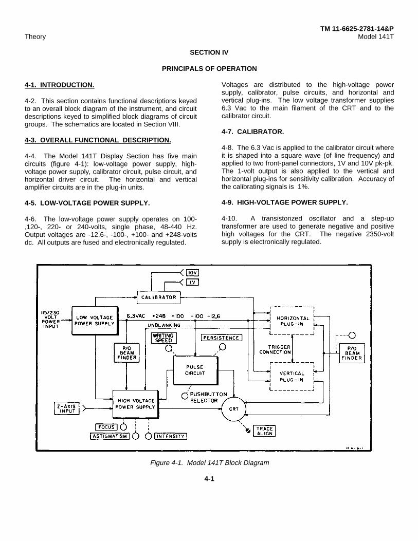
SECTION IV
PRINCIPALS OF OPERATION
4-1. INTRODUCTION.
4-2. This section contains functional descriptions keyedto an overall block diagram of the instrument, and circuitdescriptions keyed to simplified block diagrams of circuitgroups. The schematics are located in Section VIII.
4-3. OVERALL FUNCTIONAL DESCRIPTION.
4-4. The Model 141T Display Section has five maincircuits (figure 4-1): low-voltage power supply, high-voltage power supply, calibrator circuit, pulse circuit, andhorizontal driver circuit. The horizontal and verticalamplifier circuits are in the plug-in units.
4-5. LOW-VOLTAGE POWER SUPPLY.
4-6. The low-voltage power supply operates on 100-,120-, 220- or 240-volts, single phase, 48-440 Hz.Output voltages are -12.6-, -100-, +100- and +248-voltsdc. All outputs are fused and electronically regulated.
Voltages are distributed to the high-voltage powersupply, calibrator, pulse circuits, and horizontal andvertical plug-ins. The low voltage transformer supplies6.3 Vac to the main filament of the CRT and to thecalibrator circuit.
4-7. CALIBRATOR.
4-8. The 6.3 Vac is applied to the calibrator circuit whereit is shaped into a square wave (of line frequency) andapplied to two front-panel connectors, 1V and 10V pk-pk.The 1-volt output is also applied to the vertical andhorizontal plug-ins for sensitivity calibration. Accuracy ofthe calibrating signals is 1%.
4-9. HIGH-VOLTAGE POWER SUPPLY.
4-10. A transistorized oscillator and a step-uptransformer are used to generate negative and positivehigh voltages for the CRT. The negative 2350-voltsupply is electronically regulated.
Figure 4-1. Model 141T Block Diagram
4-1

TM 11-6625-2781-14&PTheory Model 141T
4-11. PULSE CIRCUIT.4-12. This circuit generates pulses of variable level andrate. These pulses and other dc voltages from the circuitare applied to the storage and persistence elements inthe CRT. The low-voltage power supply provides alloperating power for the pulse circuit.
4-13. HORIZONTAL DRIVER CIRCUIT.4-14. The horizontal driver is an impedance convertercircuit. The output from the horizontal amplifier circuit inthe plug-in unit is applied to the input of the horizontaldriver circuit, which in turn drives the horizontal plates ofthe CRT.
4-15. CIRCUIT DESCRIPTION.
4-16. LOW-VOLTAGE POWER SUPPLY.4-17. The low-voltage power supply consists of +100-volt supply, -100-volt supply, +248-volt supply and -12.6-volt supply. The +100-volt supply is independent andprovides a reference voltage for the -100-volt supply.The +248-volt and -12.6-volt supplies are dependent onthe -100-volt supply for reference voltages.
4-18. figure 4-2 is a simplified block diagram of theregulator used in the low-voltage supply. The seriesregulator acts as a variable resistance in the regulatedoutput. A sensor (or differential amplifier) compares theoutput voltage with a reference voltage. The driver(emitter follower or amplifier) controls the bias on theseries regulator, which effectively controls the seriesresistance. Any change in output voltage is fed back tothe series regulator. The change in series resistanceand the resulting voltage drop is opposite to the outputvoltage change, maintaining the output voltage at aconstant level.
Figure 4-2. Regulated Power Supply Block Diagram
4-19. figure 8-10 is a schematic diagram of the lowvoltage power supply. The primary winding is wiredthrough a rear panel power module for conversion to100-, 120-, 220- or 240-Vac operation. Line voltage is
applied to the primary of TI through an on-off switch, afuse and a thermal switch. Pilot lamp DS1, lights whenpower is applied to T1. Two shunt resistors areconnected to the +248-volt supply to reduce seriesregulator power dissipation when high-current plug-insare used. Each shunt is wired to a rear panel connector.The internal wiring of the plug-in determines whether theshunt is in the circuit or not.4-20. +100-Volt Supply. The ac voltage from thesecondary ofT1 is rectified by A1CR5-AICR8 andpartially filtered by C3 and A2R17. The resulting dcvoltage is applied through the series regulator Q2, to theoutput. Differential amplifier A2Q4/A2Q5, compares thevoltage across A2V1 with a sample of the output voltage.Any change in output voltage is applied to the base ofdriver A2Q3, which controls the bias on regulator Q2.Series regulator Q2, compensates for the change inoutput voltage by changing resistance and restores theoutput level to normal. The +100-volt output is adjustedby A2RllB and fuse A2F2 provides overload protection.
4-21. -100-Volt Supply. Reference voltage for the -100-volt supply is taken from the output of the +100-voltsupply. The reference voltage across A2R31 iscompared with a sample of--100-volt output acrossA2R35. The error voltage sensed by differential amplifierA2Q7/A2Q8 is applied through driver A2Q6, and seriesregulator Q3. The series regulator brings the -100 voltsupply back into proper balance with respect to the+100-volt supply. Ac voltage from T1 is rectified byA1CR9-A1CR12, partially filtered by C4/C5/A2R27, andthe resulting dc voltage is applied by the series regulatorQ3, to the -100-volt output. Regulation is obtained as inthe +100-volt supply. A2R11C adjusts the -100-voltoutput, and fuse A2F3 provides overload protection.
4-22. +248-Volt Supply. Sensor amplifier A2Q2, in the+248-volt supply senses any variation in the outputvoltage with respect to -100 volts. The error voltage isamplified by driver A2Q1, which applies corrective bias toseries regulator Q1. A2RllA adjusts the +248-volt outputand fuse A2F1 provides overload protection. A2CR4provides temperature compensation for A2Q2, and isnormally forward-biased.
4-23. -12.6-Volt Supply. Sensor amplifier A2 Q11senses any variation of output voltage with respect to -100 volts and applies the error voltage to driver amplifierA2Q9. The driver increases signal current to the levelrequired to control series regulator Q4. The -12.6-voltoutput is adjusted by A2R47A. Current limiter A2Q10 isa protective circuit for the series regulator and isnormally biased off. If an overload occurs across the -12.6-volt output, the base of
4-2

TM 11-6625-2781-14&PTheory Model 141T
A2(Q10 goes positive by the voltage drop across R11,minus the forward voltage drop across A2CR16, turningA2Q(10 on. The collector of A2Q10 is applied throughA2Q9 to the base of series regulator Q4, reducing thecurrent flowing through Q4. The current flows throughan external overload which limits the current required tokeep A2QIO on. Additional over-load protection isprovided by fuse, A12F4.
4-24. CALIBRATOR.
4-25. The calibrator circuit (figure 8-10) consists of threeparts: a tunnel diode (square wave generator), ;1transistor switch, and a calibration network.
4-26. Input to tunnel diode A2CRI9, is applied throughA2R5.0. The tunnel diode generates a square wave atline frequency. Transistor switch A2Q12, is off duringthe time of the positive half-cycle of the square wave(when the voltage at the base is close to zero), and thecollector voltage is at a level set by breakdown diodeA2VR6 and resistor A2R47B. When the negative-goingportion of the square wave is applied to the base ofA2Q12, the transistor increases conduction, effectivelyshorting the collector to ground. The output of thecalibrator becomes zero. At the end of the negative inputhalf-cycle (bias of A2Q12 returns to zero) the transistor isturned off, and the output returns to its previous value.
4-27. Tunnel diode bias current is supplied throughA2R51. The bias current sets an operating level for thediode which ,affects the symmetry of the square waveoutput. Cal adj A2R47R, is used to set the dc
voltage at the collector of A2Q12 to -10 volts when thetransistor is off Breakdown diode A2VR6 reduces theoutput impedance, and provides the temperaturecompensation for the circuit. Voltage divider A2R;54 ,’A2R55, reduces the 10-volt output to 1 . Roth 10- and I -volt outputs are available at the front panel of theinstrument, and the 1-volt output is available to bothplug-ins.
4-28. HIGH-VOLTAGE SUPPLY.
4-29. figure 4-3 is a block diagram of the high-voltagepower supply. The output of a regulated transistoroscillator is stepped-up in voltage and applied to a seriesof high voltage rectifiers. The positive output of thevoltage tripler is connected to the post-accelerator of theCRT. The negative output voltages are used in the gunassembly of the CRT and its associated controls. The Z-axis input can be used to apply intensity modulatingsignals to the CRT.
4-30. figure 8-13 is a schematic diagram of the high-voltage supply and the CRT. Oscillator A2Q12 operatesat a frequency of approximately 32 kHz. Any change inthe output voltage is applied to A2Q15, which convertsthe voltage change to a current change. This currentchange is applied, by emitter follower A2Q14, to the baseof the oscillator transistor. The amplitude of oscillationsis changed in such a direction as to oppose the originaloutput voltage change. high-voltage adjust A2R6:3 setsthe amplitude of oscillation to produce the correct outputvoltage.
Figure 4-3. High-Voltage Power Supply Block Diagram
4-3

TM 11-6625-2781-14&PTheory Model 141T
4-31. Two separate negative supplies are used, one forthe control grid of the CRT, and one to provide the CRTcathode and focusing voltages. Both supplies use half-wave rectifiers (A2CR23 and A2CR24). The unblankinggate from the horizontal plug-in (pin 1, J2) is applied tothe return side of the grid supply, and changes thenegative grid voltage by about +50 volts to unblank thetrace. A positive pulse of about 20 volts will blank thetrace when applied to Z-axis input. When Z-axis input isnot used, S4 is set to INT to receive chopped blankingfrom a dual-trace plug-in.4-32. The voltage tripler circuit provides the 6.6 kV post-accelerating voltage applies to the CRT.4-33. The ASTIG adjustment, R8, adjusts the roundnessof the spot, and the geometry adjustment, A2-R72, isused to optimize pattern shape.4-34. STORAGE CRT.4-35. Refer to figure 8-13 for the schematic diagram ofthe storage CRT, VI. The CRT contains the conventionalelectron (writing) gun, deflection plates, post-accelerator,and phosphor screen. In addition, there are twofloodguns, a collimator, a collector mesh, and a storagemesh. These added elements make possible thevariable persistence and storage functions of theinstrument.4-36. Flood Guns. Two flood guns are located on theelectron gun, outside of the horizontal deflection plates.Horizontal drivers, A6QI and A6Q2, prevent flood gunelectrons from flowing through the deflection plates tothe output stage of the plug-in. The guns operatecontinuously when the power switch is ON. An electroncloud, that is emitted by the flood guns, is acceleratedtoward the CRT screen by collimator and collector meshvoltages. These electrons make stored or persistingdisplay visible. They are also used to erase stored andpersisting displays.4-37 Collimator. The collimator is an internal coatingalong the tapered portion of the CRT. A positive voltageapplied to the collimator focuses the flood-gun electrons.The flood-gun electrons are formed into a columnperpendicular to, and approximately equal to the width ofthe CRT screen.4-38. Collector Mesh. The collector mesh is betweenthe flood guns and the storage mesh (closer to thestorage mesh). It is always positive with respect to thestorage mesh except in the ERASE mode of operation;both are then at the same potential. In addition toaccelerating flood gun electrons, the collector mesh alsorepels positive ions generated by the flood guns.4-39. Storage Mesh. The storage mesh is just behindthe CRT screen and is coated with non-conductingmaterial. It is statically held at a slightly positive potential(approximately +3 volts). When the electron beam fromthe writing gun strikes the mesh coating, secondaryelectrons are emitted. This secondary emission creates
a pattern of positive potential identical to the movementof the beam. Flood gun electrons are accelerated by thispositive potential pattern and strike the phosphor screen,creating a visible display.4-40. The storage mesh is pulsed with pulses ofapproximately 10 microseconds duration. These pulseserase the positive pattern on the storage mesh bydischarging the mesh coating. Time required for thiserasing operation is determined by the pulse repetitionrate. The positive pattern on the mesh may also beneutralized manually by connecting the collector andstorage meshes (erase). The high positive potential(approximately +156 volts) allows more uniformdischarging of the surface. When the storage mesh isdisconnected from the collector mesh and returned to +3volts, the coated surface is at a uniformly equal potentialof--9 volts. In both cases, the screen has no illumination.The pattern may be lost by the storage mesh fadingpositive and allowing the entire screen to be illuminated.This occurs when positive ions from the flood gun raisethe surface potential of the storage mesh in randomareas sufficiently to allow flood gun electrons to strike thescreen.4-41. PULSE CIRCUIT.4-42. figure 4-4 is a simplified block diagram of thepulse circuit. The pulse circuit supplies pulses ofvariable repetition rate to control the operation of theCRT. The pulse timer generates a pulse which triggersthe monostable multivibrator. The two outputs of themonostable multivibrator are applied to the flood gundriver and output pulser. The flood gun driver appliespulses to the accelerator of the CRT to control storagetime of the display.4-43. The output pulser applies a positive voltage to thestorage mesh of the CRT. The erase timer provides asignal to the monostable multivibrator and output pulserto generate an erase pulse and also triggers the blankingcircuit. The blanking circuit energizes a relay in the highvoltage supply which applies a blanking voltage to theCRT. The CRT collimator voltage is supplied by a linearamplifier and is controlled by the selection of the writingspeed at the front panel.4-44. STD AND FAST MODES.S-E.S. Pulse Timer. figure 8-16 is a schematic diagramof the pulse circuit. Setting the front panelPERSISTENCE control, R10, determines the amount ofcurrent available from the pulse timer current source,A5QI . A5C1 charges to a potential which turns A’5Q2on. A5CI discharges through A5Q2, A5-Q2 turns off,and A5Cl again begins to build a ramp voltage. Therepetition rate of this action is controlled by the setting ofthe front panel PERSISTENCE con-
4-4
TM 11-6625-2781-14&PTheory Model 141T
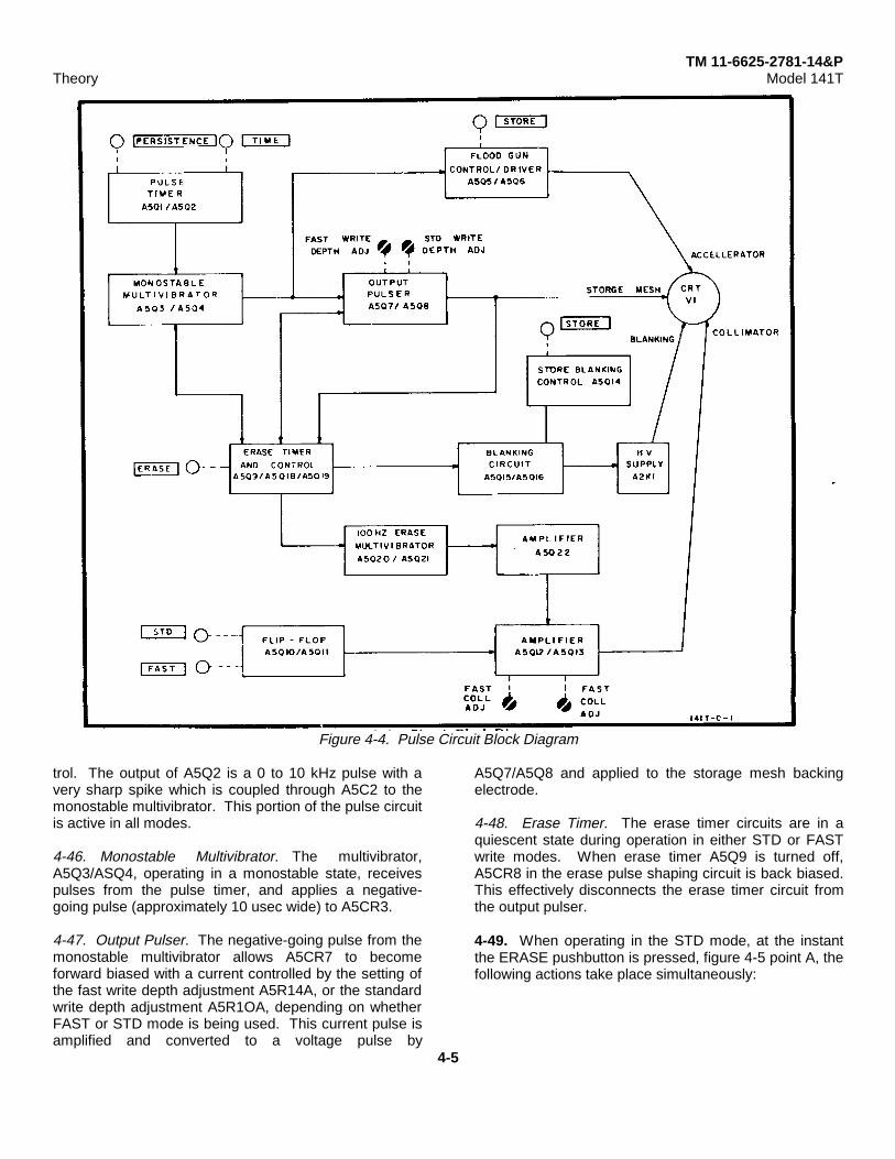
Figure 4-4. Pulse Circuit Block Diagram
trol. The output of A5Q2 is a 0 to 10 kHz pulse with avery sharp spike which is coupled through A5C2 to themonostable multivibrator. This portion of the pulse circuitis active in all modes.
4-46. Monostable Multivibrator. The multivibrator,A5Q3/ASQ4, operating in a monostable state, receivespulses from the pulse timer, and applies a negative-going pulse (approximately 10 usec wide) to A5CR3.
4-47. Output Pulser. The negative-going pulse from themonostable multivibrator allows A5CR7 to becomeforward biased with a current controlled by the setting ofthe fast write depth adjustment A5R14A, or the standardwrite depth adjustment A5R1OA, depending on whetherFAST or STD mode is being used. This current pulse isamplified and converted to a voltage pulse by
A5Q7/A5Q8 and applied to the storage mesh backingelectrode.
4-48. Erase Timer. The erase timer circuits are in aquiescent state during operation in either STD or FASTwrite modes. When erase timer A5Q9 is turned off,A5CR8 in the erase pulse shaping circuit is back biased.This effectively disconnects the erase timer circuit fromthe output pulser.
4-49. When operating in the STD mode, at the instantthe ERASE pushbutton is pressed, figure 4-5 point A, thefollowing actions take place simultaneously:
4-5

TM 11-6625-2781-14&PTheory Model 141T
a. The collector mesh potential of +156 volts isapplied to the junction of A5R27 and A5R28. Thisvoltage causes A5CR14 to become reverse-biased,which protects A5Q7 and A5Q8.
b. The +156 volts applied to A5R27 turns A5Q9 onwhich charges A5C8 to 0 volts. This action turns onASQI5 A.-Ql6 through A5R53 which blanks the CRTwrite gun by means of a relay closure on the high voltagepower supply board.
c. Zero volts on A5R17 reduces the output ofamplifier A5Q7 A5Q8 by approximately -12 volts.ASQ18 turns on, turning A5Q19 off. A5Q3 is turned onby current through A5R7 which allows amplifier A5Q7 A.-Q8 to reach its full output amplitude, less the reduction inamplitude due to the current through A5R17. The resultis approximately -4 volts. The erase multivibratorA5Q20/A5Q21 begins to free run at approximately 100Hz. This signal is amplified through A5Q22 to driveA5Q12 and A5Q13 for an alternating collimation voltageto better erase the CRT.
d. The circuits remain in this state as long as theERASE pushbutton is pressed.
4-50. When the ERASE pushbutton is released, figure4-5 point B, the following circuit actions occursimultaneously:
a. ASQ9 is turned off.b. The voltage on A5C8 begins to discharge from
approximately 0 volts toward -12.6 volts, figure 4-5 pointD.
c. The voltage change across A5R17/A5VR1causes the output of amplifier A5Q7/A5Q8 to increasefrom about -4 volts. The increase is in the form of aramp to the output voltage determined by the standardwrite depth adjustment A5R10. When A5VR1 is nolonger conducting, the ramp stops, figure 4-5 point E.
d. A5Q3 is held in saturation by A5R7. Thisestablishes the output voltage of amplifier A5Q7/A5Q8 atapproximately 8 volts.
e. When A5C8 voltage decreases to -12.6 volts,ASQ3 turns off (figure 4-5 point F), and the output
pulser returns to the quiescent voltage of approximately3.3 volts. A5Q20 and A5Q21 stop running and thecollimator voltage returns to the nominal value.
4-51. Operation of the ERASE pushbutton when in theFAST mode is as described in paragraphs 4-49 and 4-50except that the storage mesh potential drops less afterreleasing the ERASE pushbutton and remains constantuntil A5C8 voltage decreases to -12.6 volts (figure 4-5points C and B). This action results from the forward-biasing of A5CR29 which prevents current flow throughA5CR8 and allows the output of A5Q7 and A5Q8 to go toits maximum level as determined by the fast write depthadjustment.
4-52. At this point, all pulse circuits have returned to thecondition they were in prior to pressing the ERASEpushbutton, and pulses from the pulse timer may againbe applied to the storage mesh backing electrode.
4-53. PULSE CIRCUIT:STORE MODE.4-54. Flood Gun Grid Control. Pressing the STOREpushbutton removes +156 volts from A5R19 and A5R50.This turns off A5Q5 and pulses from the monostablemultivibrator are now coupled through A5C5 to the baseof A5Q6. During the 10 usec that A5Q4 output goespositive, A5C5 is charged. When A5Q4 output goesnegative, A5CR9 is back biased and A5Q6 turns off.The collector of A5Q6 goes positive until A5C5 ischarged and turns A5Q6 back on. This pulse has aduration of approximately 60 usec. This pulse is appliedto the flood gun accelerator, which turns the flood gun onfor the pulse duration.
4-55. The repetition rate of these positive pulses at thecollector of A5Q6 is now determined by the setting of theSTORE TIME control, R9, which replaces thePERSISTENCE control when the STORE pushbutton ispressed.
4-56. The write gun is blanked by A5Q16 through theaction of A5Q14 and A5Q15.
4-57. PULSE CIRCUIT:CONVENTIONAL MODE.4-58. When the CONV pushbutton is pressed, a +100-volt potential is removed from A5R25. A5CR15 isforward biased by -100 volts through A5R26, A5-CR14,and R25. This voltage divider sets the storage meshbacking electrode to approximately 29 volts. A5-CR13 isreverse-biased, preventing output pulser signals frompassing through. This action produces conventionaloscilloscope operation by disabling the variablepersistence mode.
4-6

TM 11-6625-2781-14&PModel 141T Theory
4-59. When the oscilloscope is turned off, a displaystored on the CRT is protected from unintentionalerasure by A5Q17 and the associated circuit.
4-60. TRACE ALIGN.
4-61. The trace align coil L1, is located around the CRTnear the screen. Adjustment of TRACE ALIGN R7A/B,changes the magnitude and direction of current throughthe coil and rotates the trace into alignment with the CRTgraticule.
4-62. PLUG-IN KIT FABRICATION.
4-63. The HP Model 10477A and Model 10487AAccessory Plug-ins are blank plug-in units for theinstrument. These two units permit the user to designhis own special-purpose circuits. Current available from
each of the instrument power supplies is shown in table4-1. Do not exceed the current capabilities in table 4-1.
Table 4-1. Current Capability
Supply Voltage and Current Available atJ1/J2 pin number each Jack (J1 and J2)
+248 Vdc 9 0-50 ma+248 Vdc 9 50-100ma (pin 2 must
be wired to pin 3 in the plug in.)
+100 Vdc 2 0-137.5 ma-100 Vdc 6 10-200ma-12.6 Vdc 21 0-0.9 amps6.3Vac 13-14 0-3.25amps
4-7/4-8

TM 11-6625-2781-14&PModel 141T Performance Check
SECTION V
PERFORMANCE CHECK AND ADJUSTMENTS
5-1. INTRODUCTION
5-2. This section contains step-by-step procedures forchecking the instrument specifications as given in table1-1 of this manual. A table (performance check record)is provided at the end of the performance check forrecording the measurements obtained in the first runningof the procedure. This record may be used to comparemeasurements taken at later dates with the original. Theprocedures for making all internal adjustments arecovered in paragraphs 5-21 through 5-33. A photographshowing the locations of all internal adjustment controlsis presented in figure 5-1.
5-3. TEST EQUIPMENT
5-4. Test equipment required for procedures in thissection is listed in table 5-1. Test equipment equivalentto that recommended may be substituted, provided itmeets the required characteristics listed in the table. Forbest results, use recently calibrated test equipment. Usea non-metallic screwdriver when making adjustments.
5-5. PERFORMANCE CHECK
5-6. The following subparagraphs describe proceduresto determine whether or not the instrument is operatingwithin the specifications of table 1-1. This check can beused as part of an incoming inspection, as a periodicoperational test, or to check calibration after repairs oradjustments have been made. Any one of the followingchecks can be made separately if desired.
5-7. The first time the performance check is made, enterthe results on the performance check record at the endof the procedure. Remove the record from the manualand file it for future reference. Be sure to include theinstrument serial number on the record for identification.
5-8. PRELIMINARY SETUP
a Install time base and vertical plug-ins
b Adjust time base for a free-running 1 msec/divsweep
Table 5-1. Recommended Test Equipment
Instrument Characteristics RequiredRequired For
Type Model
Voltmeter HP 738BR HO1 Accuracy: 0.1% CalibratorCalibrator Output Voltages: 1V,10V Performance Check
CalibratorAdjustment
Digital HP 3439A Accuracy: 0.1% Low Voltage PowerVoltmeter with HP 3441A Voltage Range: ±300V Supply Adjustment
Plug-in Input Impedance: 10.2M1
High Voltage PowerSupply Adjustment
Voltage HP K05 3440A Accuracy: 1%Divider Probe Division Ratio: 1000:1 High Voltage Power
Maximum Voltage: 4 KV Supply Adjustment
Oscillator HP 204C Waveform: Sine Wave Geometry AdjustmentFrequency: 80 Hz to 400 Pulse CircuitkHz Adjustment
5-1

TM 11-6625-2781-14&PModel 141T Performance Check
c Set vertical plug-in input switch to off or groundd Set Model I -11 T controls as follows:
INTENSITY.......................................... MINPERSISTENCE ................................... MINWRITING SPEED ............................... STD
e Turn instrument on and allow a 15 minute warm-up period.
CAUTION
The INTENSITY control should never beset high enough to cause blooming.Excessive intensity can permanentlydamage the CRT storage mesh.
5-9. BEAM FINDER
NOTE
The BEAM FINDER returns beam to CRTscreen regardless of deflection potentialswhen used with the 1400-series time-domain plug-ins.
When used with the 8550-seriesfrequency-domain plug-ins, the REAMFINDER has no function.
a Perform preliminary setup (paragraph 5-8)b Rotate vertical and horizontal position controls
fully cw
c Press and hold REAM FINDER pushbutton whileslowly rotating iNTENSITY cw until a trace becomesvisible.
d BEAM FINDER should return trace to CRTregardless of position of vertical or horizontal controls.
e Adjust vertical and horizontal position controlsuntil trace is centered on CRT display.
f Release BEAM FINDER
5-10. Paragraphs 5-11 through 5-14 contain preliminaryoperational checks of performance characteristics notlisted in table 1-1. Because these characteristics are notspecified, stated : results are approximate.
5-11. FOCUS AND ASTIG.
5-12. FOCUS and ASTIG controls should give a sharplydefined trace when set to approximately midrangepositions. Adjust for sharpest trace possible and leave inthat position.
5-25-13. TRACE ALIGN
a Perform preliminary setup (paragraph 5-8
b Adjust TRACE AI,IGN until trace is parallel tocenter graticule line. This condition should occur nearcenter of adjustment range.
5-14. CALIBRATORa Perform preliminary setup (paragraph 5-8)
h Connect voltmeter calibrator to vertical input
c Set voltmeter calibrator for output of 1V p-p
d Set vertical amplifier sensitivity to .I V/div
e Adjust vertical vernier to display exactly 8 di,isions of vertical deflection.
f Disconnect voltmeter calibrator
g Connect Model 141T CAL IV output to verticalinput.
h Observe deflection of 8 ±0.1 division
i Repeat steps a through g, using 10 volts fromthe voltmeter calibrator, 1 V/'div vertical sensitivity, andCAI, 10V.
5-15. VARIABLE PERSISTENCE
a Perform preliminary setup (paragraph 5-8)
b Adjust INTENSITY for normal viewing level
c Set time base to 2 sec/div and observe that traceline disappears and that spot develops a short tail.
d Slowly adjust PERSISTENCE cw and note thattail lengthens.
e. Rotate PERSISTENCE fully cw and turn INTENSITYfully ccw.
f. Observe that trace remains visible for one minute.
5-16. WRITING SPEED, FASTa Perform preliminary setup (paragraph 58)b Set PERSISTENCE to MAXc Set time base for 1 usec/div sweep
d Set time base for single sweep
5-2

TM 11-6625-2781-14&PModel 141T Adjustments
e Press FAST pushbutton and press ERASE.Observe that background appears foggy.
F Repeatedly erase and trigger a single sweep,increasing INTENSITY slightly each time, until tracewrites and remains visible for 15 seconds.
5-17. STORE TIME, FAST.
a Perform preliminary setup (paragraph 5-8).b Rotate STORE TIME to MAX.c Press ERASE.D Trigger a single sweep and immediately press
STORE.e After 15 minutes rotate STORE TIME to MIN.
Trace should still be visible.
5-18. WRITING SPEED, STANDARD.
a Perform preliminary setup (paragraph 5-8).b Press STD.c Set time base for 50 usec/div sweep.d Repeatedly erase and trigger a single sweep,
increasing INTENSITY slightly each time, until tracewrites and remains visible for one minute.
5-19. STORE TIME, STANDARD.
a Perform preliminary setup (paragraph 5-8).b Rotate STORE TIME to MAX.c Press ERASE.d Trigger a single sweep and immediately press
STORE.e After 2 hours, rotate STORE TIME to MIN.
Observe that trace is still visible.
5-20. This completes the Performance Check. If theinstrument does not meet specifications, the adjustmentprocedure which follows should be done. If this does notresult in satisfactory performance, refer to Section VIIIfor maintenance and troubleshooting information.
5-21. ADJUSTMENTS.
5-22. The following paragraphs describe procedures tocalibrate the instrument so that it will perform asspecified in table 1-1. The entire adjustment procedurecan be done in sequence, or any separate adjustmentcan be calibrated by following the steps out-
lined in the appropriate paragraph. The locations ofadjustment controls are shown in figure 5-1, aphotograph included at the end of the section on afoldout page
5-23. Use a nonmctallic screwdriver and recentlycalibrated test equipment with characteristics asspecified in tab)le 5-I. After adjustments are complete,check instrument performance by doing the performancecheck procedure at the beginning of this section. Ifdifficulty is encountered in making any adjustment, referto Section VIII for troubleshooting procedures.
5-24. PRELIMINARY SETUP.
a Install plug-ins in both compartments. Properpower supply regulation may not occur without loadconnected.
b Remove top, bottom, left side and high voltagedeck covers. All internal adjustments are identified infigure 5-1.
Voltages present in the power supplies aredangerous.
c Rotate INTENSITY, PERSISTENCE, andSTORE TIME fully ccw.
d Turn instrument on and allow 15 minutes warm-up period.
5-25. LOW VOLTAGE POWER SUPPLYADJUSTMENT.
a Perform preliminary setup (paragraph 5-24).b Adjust low voltage regulators as indicated in
table 5-2.
NOTEBecause +100-volt supply is a referencefor the other mainframe supplies it mustbe set first. Voltage may be measured onany terminal with wire color shown in table5-2.
c Recheck all supplies before proceeding. The+IOOV supply must be set as near to +1OOV aspossible.
5-26 HIGH VOLTAGE POWER SUPPLYADJUSTMENT.
a Perform preliminary setup (paragraph 5-24).b Monitor +100 Vdc supply with digital voltmeter
using voltage divider probe. Note exact reading
5-3

TM 11-6625-2781-14&PModel 141T Adjustments
Table 5-2. Low Voltage Power Supply Adjustment
SUPPI.Y ADJUST LIMIT MEASURE POINTWIRE COLOR
+1OOV A2R11B 1V WHITE/RED-100V A2R11C t1V VIOLET+248V A2R11A ±2.5V RED-12.6V A2R47A ±0.13V WHITE/VIOLET
c Multiply value obtained in step b by 23.50.d While monitoring high voltage,--2350VM( ITOR
POINT (4), set HV adj. A2R63, to obtain voltage readingequal to result obtained in step (-2350 i25V).
e. This procedure will set high voltage wit 1%,provided +1OOV supply is set to indicate exam +IOOVon digital voltmeter.
5-27. INTENSITY LIMIT ADJUST.
NOTEMethod A must be used for Model 141T’swith 1400-Series vertical and time-baseplug-ins. Method B must be used for Model141T’s with spectrum analyzer plug-ins.
Method A.a Turn power off.b Remove 1400-Series plug-ins.c Short pins 1 and 2 of upper compartment
connector, J2, together.
Voltages present in the high voltage supplyare dangerous.
d Turn power ON.e Set intensity limit A2R65 fully ccw.f Set INTENSITY to 11 o’clock position.g Press STD pushbutton.h Slowly adjust A2R65 cw until a spot is just
visible.i Turn INTENSITY fully ccw.j Turn power off.k Remove short from upper compartment
connector J2.
l Replace plug-ins.
Method B.a Turn power off.b Install spectrum analyzer plug-ins.c Set plug-ins for 0.5 ms SCAN mode and AUTO
trigger.d Turn power ON.e Turn intensity limit A2R65 full ccw, extinguishing
trace.f Set INTENSITY to 11 o’clock position.g Press STD pushbutton.h Set PERSISTENCE to MIN.i Turn A2R65 slowly cw until crest of trace is
bright with rest of trace barely visible as shown in figure5-1A
Figure 5-1A. Spectrum Analyzer Intensity Limit Adjust
5-4

TM 11-6625-2781-14&PModel 141T Adjustment
5-28. GEOMETRY
a Perform preliminary setup (paragraph 5-24)b Set controls as follows:
trigger level ..........................................autotrigger source ...................................... int (+)sweep time...........................................0.5 msec/divWRITING SPEED ................................STDPERSISTENCE....................................MIN
c Slowly adjust INTENSITY for normal viewinglevel.
d Press ERASE.e Press CONV.f Adjust TRACE ALIGN and vertical position
controls so that trace is parallel to center graticuleline
g Connect 400-kHz oscillator output to verticalamplifier input
h Adjust vertical deflection factor to obtain slightlyunder 8 divisions of vertical deflection.
CAUTION
If it is necessary to increase intensity, doso only in STD mode. There is noindication of excessive beam intensitywhile in the CONV mode and CRT meshcan be burnt.
i Adjust geometry A2R72 for best compromisebetween distortion of vertical and horizontal edges ofdisplay. Vertical and horizontal controls may be adjustedto permit viewing of edges.
j Set INTENSITY fully ccwk Disconnect oscillator
5-29. CALIBRATOR ADJUSTMENTa Perform preliminary setup (paragraph 5- 24)b Press STDc Connect O1V p-p output of voltmeter calibrator
to vertical amplifier inputd Set vertical amplifier deflection sensitivity
to 1 V/div
e Slowly increase INTENSITY to normal viewinglevel
f Adjust vertical amplifier vernier to displayexactly 8 divisions of vertical deflection
g Disconnect voltmeter calibrator
h Connect Model 141T O1V CAL output to verti-cal amplifier input
i Set cal adj A2R47B to obtain exactly 8 divisionsof vertical deflection
5-30. PULSE CIRCUIT ADJUSTMENTS
5-31 FAST MODE ADJUSTMEAITSa Perform preliminary setup (paragraph 5-24)b Press FAST pushbuttonc Turn INTENSITY and PERSISTENCE fully ccwd Set time base for single sweep so that sweep will
not occur during this portion of proceduree Set fast write depth adj A5R14A fully ccwf Set fast coll adj A5R14B so that entire flood
gun illumination pattern is visibleg Adjust flood gun grid adj A5R14C to obtain
brightest and most uniform illuminationh Adjust fast coll adj A5R14B so that flood
gun illumination just fills graticulei Set PERSISTENCE to MAXj Press ERASEk Adjust fast write depth adj A5R14A slowly cw in
small increments, erasing after each step, until a goodcompromise between no light and saturated brightness isobtained on CRT after ERASE button is pressed.
I Adjust fast coll adj A5R14B in small increments.Erase and readjust fast write depth adj A5R14A (step k)between increments until uniform fogging is obtained.
m Set controls as follows:
sweep time ......................................... 0.2 msec/divsweep ........................................normal (recurrent)INTENSITY.................................................. fully ccPERSISTENCE ................................................ MIN
n Connect 4 kHz oscillator sine-wave output tovertical amplifier input
5-5

TM 11-6625-2781-14&PModel 141T Adjustments
o Adjust vertical gain t(J obtain 8 divisions ofvertical deflection
p Adjust INTENSITY for normal viewing level
q Increase vertical gain by a factor of 10. Do notadjust INTENSITY.
r Set time base for single sweep operation
s Set PERSISTENCE to MAX
t Increase INTENSITY gradually while erasingCRT until beam writes evenly, but not to point wherebeam is always on.
u Press ERASE pushbutton until no trace remains
v Erase, and immediately arm and trigger a singlesweep The resulting waveform should be visible inside a6 x 8 division rectangle for 15 seconds. If not, rotate fastwrite depth adj A5R14A clockwise until it is. If CRT stillwill not hold trace for 15 seconds, return to step g andreduce the illuminated area to no less than a centered7.6 x 9.5 division rectangle.
w Rotate fast write depth adj A5RI14A ccw insmall increments. leave ARI14A at point farthest ccw thatpermits trace to remain visible for 15 seconds.
5-32. STD MODE ADJUSTMENTS
a Perform preliminary setup (paragraph 5-24)
b Set INTENSITY fully ccw
c Set PERSISTENCE to MIN
d. Set std write depth adj A5RIOA fully ccw
e. Press STD pushbutton
f Set time base to single sweep to prevent beamfrom sweeping
g Press ERASE for one second and release
h Turn std coil adj ASRIOB fully ccw and thatslowly cw until screen is illuminated to point I n fromaluminum ring Collimator dimples may protrude ’3 mmfrom aluminum ring but in no may come into graticulearea
i Set time base for sweep of 10 msec/div
j Set time base, fir recurrent sweep
k Connect 80-lIz oscillator sine-wave outputvertical amplifier input
I Adjust vertical gain to obtain 8 divisions verticaldeflection
m Adjust INTENSITY for normal viewing level
n Increase vertical gain by factor of 10.Do notadjust INTENSITY’
o Set time base for single sweep operation
p Set PERSISTENCE to MAX
q Increase INTENSITY gradually while eraserCRT until beam writes evenly, but not to the poi wherebeam is always on.
r Press ERASE. If CRT does not erase cople.tely, rotate std i rite depth adj A5RIOA, cw10increments, pressing ERASE pushbutton each time.Repeat until CRT erases completely.
s. If CRT will not erase completely, rotate flo gun gridadj ASRIl4C, cw in small increments, repeating FASTMODE an(l STD MODE adjustments procedures witheach flood gun grid adj increments until CRT erasesproperly.
t. Press ERASE Immediately arm and trigger a singlesweep The waveform should be visible i side a 7 x )division rectangle for 60 seconds without positive fade}(screen turning bright green). If trace is not continuous,adjust std write depth adj A5RIC cw in small incrementsuntil continuous trace is obtained
5-33. This completes adjustment procedures. Ifsatisfactory operation cannot be obtained, refer toSection VIII for troubleshooting information
5-6
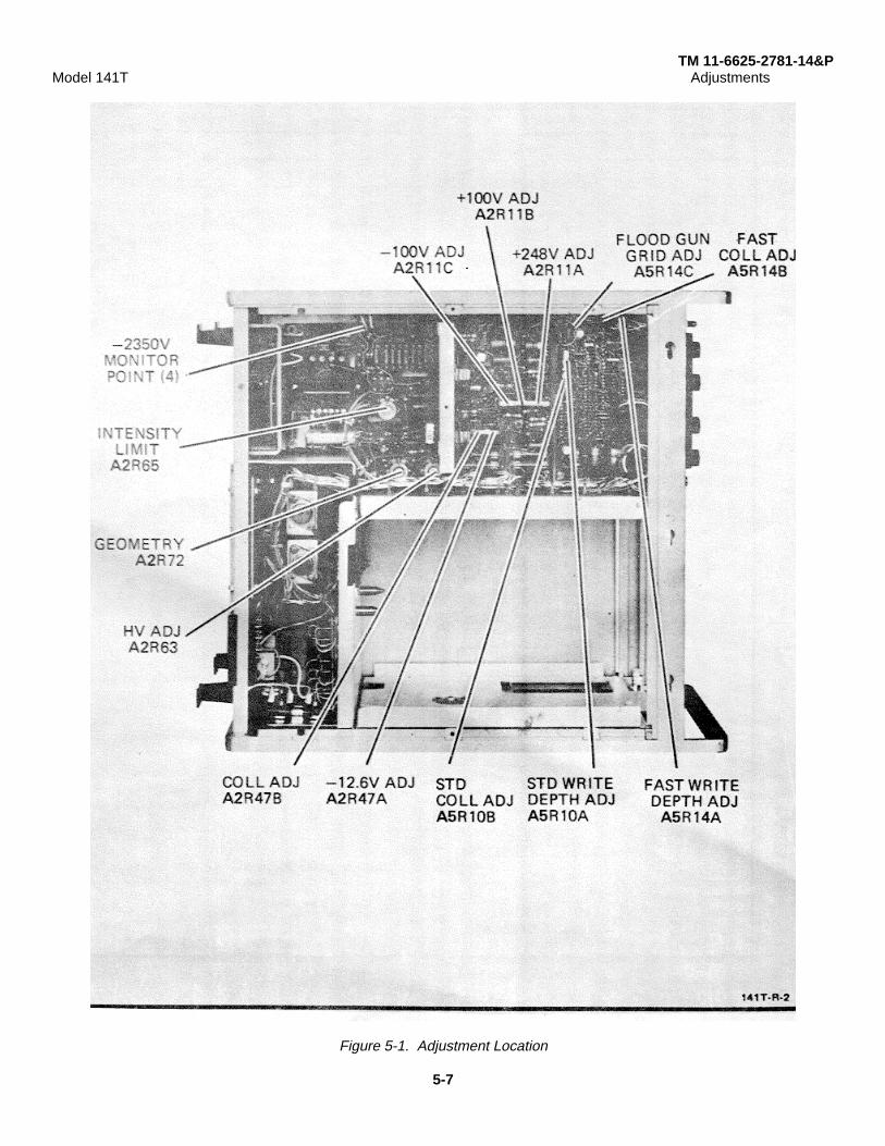
TM 11-6625-2781-14&PModel 141T Adjustments
Figure 5-1. Adjustment Location
5-7

TM 11-6625-2781-14&PPERFORMANCE CHECK RECORD
141T
Instrument Serial Number
Paragraph Check Specification MeasuredReference
5-9 BEAM FINDER Returns trace to YES NOscreen.
5-14 CALIBRATOR 8 divisions ±O.1 Divisionsdivision.
5-15 VARIABLE PERSISTENCE Spot develops short YES NOtail.Trace remains visiblefor one minute. YES NO
516 WRITING SPEED, FAST Trace writes andremains visible for15 seconds YES NO
5-17 STORE TIME, FAST Trace can be storedfor 15 minutes YES NO
5-18 WRITING SPEED, STANDARD Trace writes andremains visible forone minute YES NO
5-19 STORE TIME, STANDARD Trace can be storedfor 2 hours YES NO
5-8

TM 11-6625-2781-14&PModel 141T Replaceable Parts
SECTION VI
REPLACEABLE PARTS
6-1. INTRODUCTION
6-2. This section contains information for orderingreplacement parts. The abbreviations used in the partslist are described in table 6-1. Table 6-2 lists the parts inalphanumeric order by reference designator and includesthe manufacturer and manufacturer’s part number Table6-3 contains the lists of manufacturers codes. Table 6-4cross-references part numbers to NSN’s.
6-3. ORDERING INFORMATION
6-4 To obtain replacement parts from Hewlett-Packard,address order or inquiry to the nearest Hewlett PackardSales/Service Office and supply the followinginformation:
a Instrument model and serial number
b HP part number of items(s
c Quanity of part(s) desired
d Reference designator of part(s
6-5. To order a part not listed in the table, provide thefollowing information:
a Instrument model and serial number
b Description of the part, including function andlocation in the instrument.
c Quanity desired.
Table 6-1. Abbreviations for Replaceable Parts List
6-1

TM 11-6625-2781-14&PModel 141T
TABLE 6-2.Replaceable Parts
ReferenceDesignation
HP PartNumber
Qty Description MfrCode
Mfr Part Number
A0A1 00141-66515 DIODE BOARO ASSY 28480 00141- 665t5A2 00141-66519 POWER SUPPLY 80ARD ASSA 28480 00141- 66519A3 00141-61101 HICH VOLT AE TRIPLER ASSY 28480 10141- 61101A4 NOT ASSIGNEDA5 00141-66520 PULSE CIRCUIT BOARD ASSY 28480 00141- 66520A6 00141-66502 HORIONTAL DRIVER ASSY 28480 00141- 6650A7 5060-9421 ASSIYPDWER MODULE 28480 5060- 9421B1 3160-0252 1 FANITURE AXIAL 115V 50160HZ 16W 92702 WS2107FL-570C1 0183-0154 1 C:FXD ELE CT 43OIUF .10010: 2508-CW 56289 037361C2 0180-0012 1 C:FXD ELECT 2X2O UF 45DVDCW 56289 032440C3 0180-0046 1 C:FXO ELECT 60OUF 520VDCW 56289 032569C4 0180-0214 1 C:FXD ELECT 275 UF-50-102 20OVDCW 56289 D 36037-DFPC5 0180-0093 1 C:FXO ELECT 2OUP 1SOVDCW 56289 033193C6 0180-0213 1 C:FXD ELECT 5000 UP +75-10: 25VDCW 56289 D39556CAI 1901-0032 2 DIODE:SILICON tN3209 04113 IN3209CR2 1901-0032 DIODE:SILICON 1N3209 04713 143209DS1 1450-0419 1 LIGHT:INDICATOR SELECTED NE-2H 28480 145041gJ1 1251-0054 2 CONNECTOR; FEMALE 24-CONTACT 28480 1251-0054J2 1251-0054 CONNECTOR; FEMALE 24-CONTACT 28480 1251-0054J3 1251-2357 1 SOCKET.3-PIN MALE POWER RECEPTACLE 82389 EAC-301J4 1251 0202 2 CONNECTOR BANANA JACK 83330 2218J5 1251 0202 CONNECTOR BANANA JACK 83330 221BJ6 1210 0083 CONNECTOR BNC 0260 31221 1020J7 1510 00381 BINDINGPOST 28480 50,O38J8 1251 2366 1 CONNECTOR RANDPBPOSITIONS 71468 DCM IW8SJ9 1251 2367 1 CONNECTOR R & P.R INSERT POSITION 71468 oCM 8WRPJ10 1251 11286 1 CONNECTOR R& P 12 CONTACT FEMALE 71468 6CM 17W5JIDE 1 1251 0780 3 INSERT R&P CONNECTOR 08718 DCM 537425001J11 1251 1221 1 CONNECTOR R & P 12 CONTACT MALE 7178 DCM 17W5PJ11EI 12510179 3 INSERT R&PCONNECTOR 1468 DM 537405001L1 5060-0435 1 COIL:ALIGNMENT Z AXIS 28480 5060-0435P1 5060-0736 2 FRAME ASSY 28480 506007368P3 00141-60205 1 PANEL:FRONT 28480 00141-6020 5MP4 5060-0222 2 HANDLE ASSYSH SIDE 28480 5060-0222IAP6 5060-8735 2 RETAINER HANDLE ASSY:OLIVE GRAY(STDi 28480 50608735MPB 5060-0767 5 FOOT ASSY:FM 28480 5060-0767-llfl3 36-a ay4z 1 #TAZO 3.3m 7MP14 5000-8727 2 SIDE COVER 28480 5000-8727MP16 5060-8589 1 COVER ASSY:TOP 16LIOLIYE GRAYI 28480 506018589MP17 5060-8713 1 BOTTOM C,VER ASSY:16L FN(NINT G6R1 A 28480 5060-8713mPlA 00141-60206 1 PANEL ASSY:REAR 28480 00141-60206MP22 00140-24710 1 TOP PANEL SUPPORT 28480 0014024710PP23 0014024711 I BOTTOM PANEL SUPPORT 28480 0014024711"P24 00141-67401 1 KNOB:PUSHOUTTON ERASE 28480 00141-67401MP25 00141-67402 1 K(NO8:PUSHBUTTON FAST 28480 00141-67402MP26 00141-67403 1 KNOB:PUSHBUTTON CDNV 28480 00141-61403MP27 00141-67404 1 RCNOB:PUSHBUTTON STORE 28480 00141-67404MP28 00141-67405 1 KNOB:PUSHBUTTON STANDARD 28480 00141-67405MP29 00141-67406 1 KNOB:PUSH8UTTON 6EAN 28480 00141-67406NP34 03600015 2 SOARD0TERMINAL 76530 332-14-03411MP37 1200-0037 1 SDCKET:CRT 14-CONTACT 28480 12000037MP38 1200 0044 3 4 INSULATOR TSTR MOUNTING (TO 31 INCLUDES 71785 213011
SOCKET TRANSISTORI NSULATOR BUSHING, NYLON 26365 9 74 307
NP42 1200-0088 4 INSULATOR:00C:E 71785 293201MP46 1200-0408 1 COVER:CRT SOCKET 28480 1200-0408MP47 5020-0476 1 BEZEL:CRT 28480 5020-0476MP48 5040-0440 1 CDVER:CRT SOCKET 28480 50400440MP49 5040 0501 1 SHIEL0;LIGHT 28480 5060053MPSO 5060-0428 1 FLTER ASSV:AIR 28480 50600428MP56 0011.000104 1 GUSSET-SIDE 28480 0014000104MP58 0014001201 1 BRACRET:LATCH 28480 0014001201MP59 0014001206 2 BRACKET:FAN 28480 00140-01206MP61 0014001208 4 BRACKET:PANEL 28480 0014001208MP57 NOT ASSIGNEDMP65 00140-01209 2 BRACKET:GUSSET 28480 00140-0120gMP67 001401OZLO 2 BRACKET-TRANSISTOR Includes MP38 28480
0014001210MP69 0014024103 4 SUPPORT:PANEL BRACKET 28480 001424703
6-2

TM 11-6625-2781-14&PModel 141T
TABLE Replaceable Parts(Cont’d)
ReferenceDesignation
HP PartNumber
Qty Description MfrCode
Mfr Part Number
HP73 M00140-29902 1 PAL:EXT:UOED 28480 00140-Z9902MP74 00141-00102 1 DECK:VERTICAL 28480 00141-00102HP75 00141-00103 1 GUSSET:CENTER 28480 00141-00103HP76 00141-00104 1 DECK:IMAN 28480 00141-00104MP77 00141-01207 1 8RACKET:OIOOE 28480 00141-01207PT78 1400-0068 3 CLIP:FUSE 75915 104002KP79 00141-01203 1 8RACKET:CAPACITDR 28480 00141-01203MP88 0014I-01204 1 BRACKET:RESISTDR 28480 00141-01204MP89 00141-01208 1 8RACKET:RESISTOR 28480 UU141-01208MP90 00141-04101 1 COVER:C&PACITOR 28480 00141-04101MP91 00141-04104 1 COVER HIGH VOLTAGE BOARD 28480 00141-04104MP93 00140-60602 1 SHIELDASSY CRT 28480 0014060602MP94 0014161206 1 8RACKETASSY CRT 28480 0014161206MP95 0018001218 2 8RACKET COIL 28480 001218 012MP99 160B-1 lOB 2 GUIDE PLUG IN 28480 161B-11 0 BKPIOS 1200-0050 10 CONTACT:CRT SOCKET 72825 9553-1PII6 1410-0052 2 8USHNhG:POTENTIOMETER 28480 1410-0052KP117 5040-0709 1 TRIM:PLASTIC HANDLE 28480 5040-0709HP118 5040-0710 1 TRIMHPLASTIC HANDLE 28480 5040-0710HPII9 1490-0030 1 STNOD:TILT 28480 1490 -0030P120 1520-0042 4 MOUNT:SHOCK 00000 080D8PZ11 5040-0421 Z INSULATOR COVER:POTENTIOMETER 28480 5040-0421HP124 5000-0053 2 PLATE:FLUTED ALUMINUM 28480 5000-0053P125IZ 00141-21001 4 FEET:REAR LONG 28480 00141-21001MP126 50008015 1 SHIELD FAN, 28480 5008015D01 18530252 1 TSTR SI PNP 04713 SJ179802 1854-0294 3 TSTR:SI NPN 04713 SJ-131803 1854-0294 TSTR:SI NPN 04713 SJ-131804 1854-0294 TSTR:SI NPN 04713 SJ-1318RI 0687-3331 I R:FXD COKP 33K OHM lu4 112W 01121 E8 3331R2 0815-0031 1 R:FXD WW (2X1200)2400 OHM 5S108 28480 0815-0031R3 0811-2030 2 RSFXD WW 14 OHM 5SIOW 28480 0811-2030R4 0811-2030 RIFXO Hw 14 OHM SS IOw Z8480 0811-2030R5 2100-2962 1 R:VAR COKP 1.5 EGOHM 30S LIN 12W Z8480 2o100-o2962R6 2100-0374 1 RSVAR COMP G5EGOHM 30S LIN 1I2u 28480 2100-044R7 2100-0445 1 RIVAR COMP CANCED ZK OHN 30S LIN 1/2W 28480 2100-03 7 5R8 2100-0015 1 R:VAR CIIP 500K OHM LIN 1/4 28480 2100-0015R9 2100-2897 2 RVAR CERNET I NECOH201ZO LIN Z2 28480 2100-RI0 2100-2897 R:VAR CERMET 1 MEGOHK 20 LIN Z2 28480 2100-2897R11 0811 2994 4 1 R FXDWWDO27OHMS3%5W 28480 0811 2994S1 3101-0056 1 SWITCH TOGGLE DPDT 27191 8926K316S3 3103-0009 SWITCHITHERNAL SPST 01295 20700L1-205S4 3101-0011 I SWITCHTSLIDE DPDT 82389 111-1013S1 9100-3285 1 TRANSFORMERSPOWER 28480 9100 -3285T82 0360-0015 BUARODTERNINAL 76530 332-14-0,-011T83 0360-0012 1 STRIP:TERMIIAL, LUG TYPE 06540 628-13VI 5083B2587 1 CATHOWE RAY STORAGE TUBE 28480 50832587W1 8120-1538 1 CABLE ASSY:PDER 7.5 FT 28480 812-1538V2 00141 61632 1 CAOLEIMAIN 28480 00141 61632W3 00141-61624 1 CABLE:TWIN LEAO AS4Y 28480 00141-61624W4 001L41-61625 1 CABLE;TwIN LEAD ASSY 28480 00141-6162585 00141-61622 I CA8LE:COAXPXO MAIN CABLE 284a8o 00141-61622H6 00141-61623 1 CA8LE:COAX, PZO MAIN CABLE 28480 00141-61623o10 00141-61627 1 CABLE ASSY 28480 00141-61627U1 5Q10-0521 I CABLE ASSY 2849)1 5060-0521WllIMPI UblO1 2 HING RE IAININGFOR 0 188’ DIASHAFT 79136 510018-C MDWlIMP2 0014023101 2 PIN GUIDE 28480 00140-23101W12 50#18b 1 FLEX CIRCUIT (HVI 28480 5060 1686MP92 00141-04105 SIDE COVER:HIGH VOLT BOARD 28480 00141-04105MP97 00140-24712 SUPPORT:CRT SHIELD 28480 00140-24712MP127 1400-0651 FOOT:MDUNTING 28480 1400-0651
6-3

TM 11-6625-2781-14&PModel 141T
TABLE Replaceable Parts (Cont’d)
ReferenceDesignation
HP PartNumber
Qty Description MfrCode
Mfr Part Number
Al 00141-66515 1 DIODE GUARD ASSY 28480 00141-685Alci 0150-0052 8 CSFXD CER 0.05 UF 203 40OVI)CW 56289 33C17A
DIODE 80AAO ASSY 11 OI-hlAIdI 0150-0082 8A1Cz 0150-0052 CZFXD CER 0.05 UF 20: 400VOCW 56289 3317CIAICS 01-0052 rCPXD CEII0.05 UF 201 600VOCW 5629 33C117ALCRI 1901-0028 13 OJ00E3SILICOD 0.75£ .03PiV 04T13 S113589AtCR2 1:0011-.0110: 0100E:SILICON 0.75£ 40.PIV 04713 S 51358-9AIC:3 1901-0028 :O 0::SILICDN 0.75£ 403P1V 04713 SR1358-9AlC14 1901-028 OZOOESILICON 0.75£ 403PiV 04713 S11359AIdS 1901-002: DIODEISILICON O.75£ 403PIV 04713 SR1515-9C 4 1901-002 DIEIILCO 0.7 O V 1 3-AIIC. 61901-00 2 DIDEISILICON 0.75£ 400PIV 0713 1358-9AIIII 1901-0028 DIOOEISSLICON D.15£ 403P1V 04713 1R1358-9Al R9L 1901-0021 I00ESILICON 0.15£ 400PIV 04713 513589AlCRIO 1901-0024 DIDOI1EILICON 0.75£ 403PIV 06713 Sil355-9ALCISL 1901-00 OOOE0100SILICON O.TSA 400PIV 04713 511358-9AICRI2 1901-0028 DIODESSILICON 0.75A 403P1V 04713 151358-9A2 00141-6519 1 POWER SUPPLY BOARD £1SI 28480 00141-665191C1 L0160-016 6 C:FX0 AT 0.1 UF LOX 200VOCL 56289 192P7104920T512 0160-0168 CIPXO N9Y 0.1I UP 103 20OVOCW 56289 9P09-T12C3 0160-0168 C:SFX NY 0.1 IW 101 LOXVDCW 56289 192P10492-PTS514 LBO-0100 2 CZPXD ELECT 4.7 UP LOX 35VDCW 56289 159OD4 7SX903592-BYZC5 015o0082 C3PXD CEN 0.05 UF 202 400VOCW 56289 33C17A£216 OL6I Ot*8 CBFXO Pl 0.1I U 103 2O3VDCW 56289 192P1D492-PTS51c7 0180-0100 C:FXD ELECT 4.7 UF LOS 35VOCW 56289 1500475X 903552-DY1AZES 0160-0157 1 CIFXD MY 0.0067 UP 103 ZOOVDCW 56289 192P47292-T112C 9010-0097 1 CSPXD TANT47 UF law 35VDCW 56289 1250046X903SS2-3YS21c10 auld-0138 1 C FXD ELECT 100UF100-1(j 4OVDW 284805111 Obu-0230 1 CIPFOXIOLECT 1.0 UP! 203 60PV 4W 22112 015000032 CPFXD CER 0.05 UP 203 SOOVDCW 56289 33CIT712C13 01£00151 5 CPIFD CEI 4700 PF +80-203 4OOVDC01 71590 DAO4-040OCD5114 0160-0151 CFIXD CER 4700 PP -80-203 400OVDCW 71590 D l045-040CO5115 0160-0151 CXFID CE1 4700 PF +80-003 400OVDCw 71590 A04,040OCD£2cl6 0160-0907 a CPFXD CER 0.01 UF .80-203 SOOvocu 14655 THSOR123Z-112C17 0DI"0907 CIPID CEPt 0.01 UP #-20X SO00OVDCV 1465S T1150R123Z-IAzca 0160-0151 CIFXD CIER 4700 PF +80-20 40OOOVDCW 71590 D 066-0401CO£1A 9 OL160-0151 CBPXD CERt 4700 PP +80-203 400OVDCW 71590 A048-04OCD0£2120 0160-3448 1 C FXD CER 1IOOPF 10% 10O(OVDCW5 6 289 C067B251F102KS25 CDA2C21 0160 3443 C FXD CER 0 I IF 'OVDCW 72982 8131 5C 651 Ud 7A2CR2 1901-0040 30 IOODEISILNCOO 50 KA 30 WV 07263 FDP010sA21R3 1901-0040 DIODDESILICON 50 PA 30 WV 07263 FDCIOSI£2Cf4 1901-0096 1 DIDOEISILICON IZOV 01295 Lr-sasAZCR5 1910-O016 2 DIODESGE 40 WIV 28450 19100016£2C18 L901-0026 2 OIOOE:SILICON 0.75£ 203P1V 04713 511358-£2C110 1901-0040 DIDDE2SILICON So PA 30 WV 07263 P010881ZCRI L1901-0040 DIOODFSILICON So N£ A0 WV 07263 PFDrY18A12C13 1901-0040 DIODESSILICON 50 MA 30 WV 07263 FDGI089A2C114 1901-0040 OZOOESSILICON 50 PA 30 WV 07263 FDGIO02C1k15 1901-0026 CIOODESILICON 0.75£ 200PIV 06713 SR1358-5A2CR16 1901-002S I DIDDESILICOP IOOMA/1v 07263 2387A?1C1R 1910-0016 OIODEIGE 60 WIV 28480 1910-0016AZRIS 19010040- ODOOEID SILICON 50 PA 30 WV 07263 FDGILI£12Ck9 2912-000' 1 DIODE TUNNEL:GERMANIUM 03508 IN3718 SPECAZCR121 1901-0040 DIDERSILICON 50 PA 30 WV 07263 FOGIOSI£51822 1901-009 1 DIDOOESILICON 5OPIV 28480 1901-0049A2C123 1901-0341 2 DI0DE0SI 1000 PIV S0OM 28480 1901-0341A2CR24 1901-0341 DI0DE0 SI 7000 PIV S0OM 28480 1901-03411ZCRZS 1901-0040 DIODE:SILICON 50 sA 30 WV 07'63 FDG0188ZCR126 1901-0436 2 DIODE3SILICON 1600 PIV 28480 1901-0636A2CR2 1901-0436 OIDOE:ISlLICON 1600 Ply 28480 1901-0436A2CR21 1901-0029 D1IOOE:SILICON 600 PIV 28480 1901-0029A2FI 21I0-0067 1 FUSE:0.30A 250Y 28480 2110-0067A2F2 2110-0033 1 FUSE:0.75£ 250W 75915 F02GR750AA2F3 2110-0012 1 FUSE:0.5 AMP 250V 75915 312.500A2F4 2110-0003 1 FUSE:CARTRIDGE 3 AMP 3 A6 75915 312003A2KLI 0490-0191 1 COIL.RELAY 600 OHM NOV12V DC 71707 u-2P \fs10 0A2L1 9140-0171 1 COIL:ID 40 UN 103 1 82142 10608-1A.L2 9140-0210 1 COIL PXD RF 100 UH 5% 71895 1537 76AgtPI 0340-0451 1 WASHER:INSULATED TRANIS TOR 04713 143 5260OP03A2MP2 21D-0269 a CLIP:FUSE 0.2H50- D£ 91506 600-532C1
6-4

TM 11-6625-2781-14&PModel 141T
TABLE 6-2. Replaceable Parts (Cont’d)Reference
DesignationHP PartNumber
Qty Description MfrCode
Mfr Part Number
A2MP3 5040-0401 2 SUPPORT, CAPACITOR 28480 5040-0401A2M(P4 510410-0430 1 MOUNT TRANSFORMER BOTTOM 28480 5040-0430A2MP6 0120-01101 1 NEAT SMIN:T£NSI£STOR 28480 0120N01101AZ:P4 5040-0402 1 MOUNT TRANSFORMER TOP 28480 5040-0402A201 1854-0005 TSTR,SI 80131 2840131A202 1853-0036 1 ISTYIRS npn 80131 2N3906A203 1853-0022 1 TSTR:SI MP- 07263 S17843A203 1854-0087 1 TST4S MPN 80131 213417A205 1854-0071 20 TSTRSSI HFHNSELECTEO FIOM 3N37041 28450 1854-0071A205 1854-0022 TSTR:SI MPME 07263 517843A207 1854-0071 TSTRSSI NPN(SLECTEO FROM ZN3704) 28480 1854-0071A20 1854-0071 MU STRSSI NPN(SF8ECTED FROM 213104) 28480 1854-0071A206 504-0302 TSTR,SI 07263 S17843A209 1854-0039 T TSTRSSI MPH 80131 2N3053A2010 1854-0021 TSTR:SI NPN P 80131 313904A2011 1854-0071 TSTR:SI HPNISEIECTEO FROM 3N3104) 28480 1854-0071A2012 1850-0299 1 TSTR:NPN F 80131 1TR*964A2012 1853-0089 1 TSTR:SI NPN 80131 214918A2014 1853-0034 1 TSTR:S1 PHP(SEIECTE0 F213251) 28480 1853-0034A2015 1855-0057 1 TSTR:SI FEI N-CHAN NEL 28480 1855-0057A281 0687-1041 1 RTFXD COMP 100% OHM 101 113' 01121 ES 1041A282 0164-0033 1 RSFXD MET ox 33 GM 51 23 28480 0764-0033A2R3 0761-0007 1 R:FXO MET OX 27K OHM1 5 1W 284280 0761-0007A2R4 064-102 1 RFCOP 10010 1 C 21A285 0683-1015 1 R2 FxI COI F 100 OHM 53X 1/4W 218 41C8 1015A286 0757-0044 2 R:FXD MET FIN 33.2% OHM 13112W 28480 0757-0044AZR1 0757-0401 5 R:FX0 MET FIN 100 OHM 13 I/SW 28480 0o57-0401A2R8 0757-0243 2 RIFXO MET FIN 3.01% OHM 13 1/8W 28480 0757-0273A289 0757-0467 2 R:F%0 MET FIN 100% OHM IO 1/8W 28480 0757-0465A2810 0757-0370 2 R:FXD MET FLM 49.9% OHM 1.03 1/cs 28480 0751-0370A2111 2100-1589 1 RIVAR COMP 7K/3%l5/ OHM 20 LIN 1/4W - 28480 2100-1589A2R12 0757-0361 2 R:FXD MET FLN LOOK 04HM I 113' 28480 0751-0367A2R13 0757-0401 RSFXO MET FIN 100 OHM 13 I/SW 28480 0761-0401A2814 0766-0033 1 R:FXD MET FIN 2000 OHM 23 3W 28480 0766-0033£2815 0757-0434 1 RSFXO MET FIN 3.65% OHM 13 1BW 28480 0757-0434A2R16 0761-0006 1 R:FXD MET OX 10OK O4M 53 1W 28480 0761-0006A2817 0681-5631 4 R:FXO COMP 56K OHM 103 1/21 01121 18 5631A2R19 0684-1021 RSFXO COMP 1000 OHM 101 1/411 01121 C0 7031A2820 0757-0 399 P2 RSFXO MIT FIN 52.5 OHM 13 1/8W 28480 0757-0399A2821 0684-0621 1 R:FXD COMP 5.6 OHM 1OIE 1/4 01121 CO 5621A2822 075T-0764 2 RFXID FIN 33.2% OHM It 1V/S 28480 0757-0764A2123 0157-0388 3 R:FXD PIN 50.1 OHM 13 118W 28480 0157-0388A2823 0757-0388 3 RXFD FLNI 30.1 4.2O 13 I/SW 28480 0757-0436£2826 0o51-7046 3 R:FXO MET FLN 22.1% OHM 1.03 II1W 28480 0757-0846A2827 078-5671 04 3 :FX COMP 56% OHM 103 1/2W 01121 EB 5631A2828 0681-5631 RSFXO COMP 56K OHM 103112W 01121 W 8 5631A2829 0687-1521 RZFXO COMP 1000 OHM 103 112W 01121 Co 1021AZA29 0156-0199 RIFXO MET FIN 82.5 OHM 10 1/4W 28480 0757-0399A2A31 0757-0390 R FXO MET FLM 49 9K OHM I 0% 112W 28480 0757-0370
MUST BE REPLACEOAS A SET FOR PROPER RESULTSA2R32 0757-07O2 1 RSFXO MET FL" 68.1% OHM 13 1/4W 28480 0757-0112£2833 0757-0388 RTFXD FIN 30.1 OHM I3 I/8W 28480 0757-0388£2834 0751-0436 RFFXD MET FIN 4.32% OHM 13 1/8W 28480 0151-0046
ANO A2RII MUST SE REPLACEOAS A SET FOR PROPER RESULTS
£28(36 0757-0764 R:FXO FIN 33.2% OHM 13 114W 28480 0757-0764A2838 0727-0431 8IFXo DEPC 2.69K OHM 13 113 28480 0727-0431A2839 075T-0846 RIFXD MIE FIN 22.1% OHM 1.01 1/I 28180 0E5R-0826A2R40 0681-2221 1 R:FXD COMP 2200 OHM 109 1/3' 01121 E8 2271A2R41 0687-4131 1 IRFKO COMP 471 OHM 103 113' 01121 18 4731A243 0157--0846 RI-FXO MET FIN 22.1%( O 1.03 2W- 28480 0757-0846A2R44 0757-0190 1 8:FXO MET FIN 20K OHM 13 1/2W 28480 0757-0190A2845 0757-0480 3 8:FXD FIN 432K [H)M It 118W 28480 0151-0380A2846 0757-0388 R:FXO FIN 30.1 OHM I; 118W 28480 0157-0388A2R47 2100-1588 1 RIVAR CI]MP 2 X 1.5% OHM 303 LIN lf4W 28480 2100-1588A2848 0757-0273 R:FXD MET FIN 3.01% OHM 13 1I/W 28460 0751-021A2849 0811-1L46 1 R3FXD WW 0.36 OHM SX 2W 28480 0811-1746AZR50 075S-0421 1 R:FXD MET FIN 825 OHM 13 I/SW 28480 0757-0421A2851 0757-0428 1 RIFXO MET,FIM 1.62K UHM It 1/8W 28480 0751-0428A2852 0761-0075 1 RIFXO MET OX 16K OHM 51 1W 28480 0761-0075£2R54 0698-3555 1 R:FXD MET FIN 4.437% OHM 0.53 113' 28480 0698-3555A2855 0698-3554 1 RIFXO MET FIN 493 OHM 3.53 1/2W 28480 0698-3554A2856 0684-3331 1 R/FXW COMP 33% OHM 103 1/S 01121 CS 3331A2851 0158-0054 1 RIFXO MET OX 330 OHM 51 1/3' 288 0158-0054R2P58 06 8 4- 1 0 2 1 R2FXO COMP 1000 DNA 10 1 / 4 W -6-5£2858 068-1021 RIFXO COMP 1000 OM 103 114 01121 CS 1021
6-5

TM 11-6625-2781-14&PModel 141T
TABLE 6-2 Replaceable Parts (Cont’d)
ReferenceDesignation
HP PartNumber
Qty Description MfrCode
Mfr Part Number
A1261 OTT-O845 2 RTPXD PIN 1.18 NPGMOH IN IIZV2U480 0721- 0845A4142 0717-07 1 R:FXD FLM 90OK OHM % 112W 28480 0757MQO57A121:63 2100-0096 1 I$VA 1NEGOM 3004LIN II 2840 2100-0096A2R£4 06:-1539 1 RIFXD COMP I5K OHM 53 1141 01121CB1535A2145 216-2108 1 18161CONE 1. INEON 103tLINW 28480 2100-2108A 2 069£ 1 FLPI 13NGEOHG SN 1w 28480 06956660AZ 670171-0344 2 NET FIL 1.00 NEIOHN 13 114W 28480 017-0344Az0 0741-04 1 RSFXD MET 20K OH M 11I 28480 0004A21 0757-839 1 FIPID MET FIL 1DK OHIN 1(2w 25480 15-0439AT110 0151-0168 1 :PFXD PIN 41.51 OHMIN 1(4 28480 0?57-0168£2111 0715-0454 1 MET PIN 33.21OHM 13 11/S W 8481 0157-0454A2:72 2100-0095 1 18VAR CORP IOCK OHM 303 LIN 1i5w 28480 21001-095£2 73 0121-0845 I PID FLIN 1.18 NESMIN 13 12W 25480 0127-0845A2:74 a68-33 8 FXD FLIN 2.49 NEOHNX It 1IZW 28480 06983553AZ17 TS 98-3513 PIN 2.49 NEOOHN 13 I/W 28480 06983553£2116 0698-3553 PIN 2.49 NEGONN 18 i: 2U480 069835553A2476 0698-353 IPFXD FLN 2.49 NEOOHN 13 1(2W 25480 06983553A2*74 0696:-353 RIFXO FLP2.49 NNGOHN I2 112W 25480 06983553Aaa?9 565-3593 IRXO FIN 2.49 NEGWN It 1121 2840 0698-3553£2180 069-3553 IRPXD FIN 2.49 NEWM IIIN 1ZW 28480 0698-353£2181 0698-3553 MIPID PNFL 2.49 NEGONGH 18 1IZU 28480 0698-3553£2R&2 0751-0344 MET FIN 1.00 NEGHN II1 1141 28480 057-03,44£2881 0151-0432 1 :IPID NET FLN 27." OHM 1N 18I/ 28480 0151-0452A2P&4 01DS04065 RIFD MET FLAIN00K OHM 11 1(81 28480 0757-0465£2885 Ob8-2221 4 IPIXD 2200 ONPI 109 114V 01121 CO 2221AZA&6 06986286 1 IPIXD COMP 100 NEGONN ION 1/41 20480 0698-6286A2TI 00141-61102 1 T1ANSFORNMR ASSY 28480 00141-61102A2VI 194-l 013 I ELECTRON TUE8Z.0 */- IV 14276 18211£21v 2140-0014 3 LNPIGILOW 0.5 NILLIANP T-12 88 n11744 4A*(NM96)£213 2140-014 LAIMPILDW 0.8 NLIIIAM T-2 *UL8 11744 4A&(%E-961£214 214L0-004 M PIIPGLOIN (3 NILLIIAMPS T-2 SI 111744 44AB8-96)£2111 1902-1202 1 DIODE DiREKDOWN80.61V 28 28480 1902-3402£2112 1902-0034 1 DIODEIS.161 ION 28480 1902-0034A21118 1902-3104 2 D010DS8REAKDOWI 5.62V St 04113 SZ109931I0£2V14 1902-3385 2 01008 AREAK0011869.81 23 28480 1902-3385£2111 1902-3388 DIODE 01008A DOWE69.8V Z 28480 1902-3385A1ZV 1902-0064 1 DIODE 28480 1902-0064A3 00141-61103 1 HIGH VOLTAGE TRIPLIR ASSY 80 0114161103A3MP2 0018147101 2 GASKET- SIDE 28480 0018147101A3MP3 00181-47102 1 GASKET CENTER 28480 0018147102AS 01)141I20 I PULSE CIRCUIT BOARD ASSY 2890 0041-M20A5CI 01000118 1 C. FXD MY 0 0058 UF 10% 20DVDCW 528215 192P56292-PTSA4 NOT ASSIGNEDASCI 0140-t 158 1 CIPID MY 0.0056 UP 103 ZOOVDCW 56289 192P56292-TSASC2 01682212 1 CIPID MICA 560 PP 5N 300V01W 28480 0160-212ASC3 014G0O20 I C: FXD MICA 47 PF 5% SOOVDCW 14655 RDMI15E47WSCASC4 01401-0 I C&FXO NICA 330 PP F3 28480 01400207SCS o-0168015I 1 CIFPX MY 0.001 UP 103 56289 I92P10292TSASC& O1682262 IL CIFXD CER 16 PF S3 t00tDCW 12982 301-080 CORO 160IASC7 O1682146 1 CIPIL CEI 0.02 UP *#-20N 1000VDCW 91418 1£ASCO 0160-228 1 CISXD ELECT 22 UP 103 151101 56289 1500226N9015B2-DYSASCIO 0180-0376 1 CIPID 0.41 UP 108 3IVDCW 56289 1500741X9031A2-DYSASCII 01680160 CIFID MY 0.1 UP I1N 200VDCU 56289 192P104928TSAC12 010 168 CIPID NV 01 UP 10I O$OOVDCU 56289 192F104928TSASC13 ol0001o 1 C: FXO ELECT 2.2 UF 20% 2C1DCW 58215 1D00225X012OA2-DYSASC14 01000157 1 c: PXD MY 4700 PF 10I 200VDCW 58299 129P47202PTSAOCI 5 0101735 2 C: FXD ELECT22 UF 10%20C 28480W 01801735A2R44 010W1735 C: FXD ELECT 2 UF 10171DVcB 2848 018D-1735ASC17 010 C: FXD CER 0.05 UF 20% AMDCW 521281 33C7ASC1I noi9 4 DIOD&IS$I[LON 50 IP 30 W V 07263 1011088ASClk2 1901- 0 DIODE:SILICON 50 30 WV 07263 FP11108ASCRI 19010040 DIODESSILICON 50 PA 30 WV 07263 P0F108ASCPA 1901-0040 DIOOEISILICON 50 *A 30 WV 07263 P06108'ASCIS L19010OO DIODEISILICON 50 PA 30 WV OT1263 P61088£ICM 1901-0040 DD0EESSILICON 50 PA 30 WV 01263 FOIO8ASCIKT 19010040 OIODESILICON 50 N£ 30 WV 01263 P061088£ICl8 19010040 DIOOEISILICON 50 PA 30 WV 07263 P061088AISC 19010040 DIODEISILICON 50 MA 3J WV 07263 FOP1088£ICRIC t1l o010 I003ISIILIC.ON 50 MA 30 WV 07263 P0IOGGASCILI 941-Q040 DIODEISILICON m 30 WV 07263 P061088ASCRIZ 1901-0035 0I0D3:ILICON 181111 01263 FD3369ASC113 1901-0013 DIODEOSILICON loom 181W1 01263 P03 369£SCRI4 180-0038 OIGSSI LICON *.15£ 480PIV 104113 513559
6-6

TM 11-6625-2781-14&PModel 141T
TABLE 6-2 Replaceable Parts (Cont’d)
ReferenceDesignation
HP PartNumber
Qty Description MfrCode
Mfr Part Number
ASCR16 1901-040 OIOOEISILICON 50 MA 30 WV 07263 FOG1088ASCRI: NOT ASSIGNEDASCII t19010040 IOOETSILICOM 50 P 30 WV 07263 F0GI88A C is 1901-0040 0IOE:SILICON 50 K 30 WV 01263 F0GL08ASCRG 1901O£0,, O!ODE:SILICON 5O M£ 30 WV 07263 P0G108ACSC20 1901-0040 0IOIEISILICON 50 al 30 WV 01263 FDG1088ASC 21 1901-O40 DIODE:SILICON 50 KA 30 WV 07263 P0G10L8ASCR22 1901-0040 DIOOESSILICON 50 MA 30 WV 07263 FOGLOSSASCR23 19501-040 DIODEASILICON 50 MA 30 WV 07263 FD6108SCR24 19OL-01040 IODE:SILICON 50 M30 WV 07263 FDP6088SC5125 1501-0040 DIODESSILICON 50 MP 30 YWV 07263 P0610ASCR26 1 010414 1 0IOE8:SI 3£ 400PRRV 04713 SR1846-12SCRZ7 1901-0033 DIODESISLICONOONA0 law* 07263 F03369SCR24 1901-0040 DIGGE]SILICON SM 30 WV 01263 FOG1088ASCA29 19010D040 DIOOE:SILICON 50O L 30 WV 07263 FO61088ASLI 9100-1630 1 COILICHOKE 51.0 U) St 28480 100-1630A501 1653-00Z0 1 TSTRISI PNP(SELECTED FROM 2N3702) 28480 1853-0020A502 1:5$-311 1 TSTRSUINJUCTION SI 047113 84894A503 1 400711 ISTR3SI MPISELECTED FRON OM:3704) 28440 toC0071A504 18540071 TSTR:SI HPN(SELECTED FPROM 237041 28480 18510071ASGS 1854-0071 TSTRISI NPNISELECTED FROM 2N3704) 28480 1is-0071AS"6 1854-0350 3 TSTR:SI NPN 28480 1854-0358£507 1850358 T3TRSK NPN 28480 1850358ASO8 1454-03S$ TISTRISI N 28480 1854-0358A509 18541-001 TSTR:SI MPN(SELECTED FROM 2Z3N304 28480 1854-0071£5010 1854-0071 TSTRISI HPM(SELECTED FROM 2:3704) 28480 1854-0071A5011 3454-0071 TSTRSSI MPL(SELECTED FPROM Z37041 28480 1854-0071A5012 1854-0071 TSTRSSI NPN(SELECTED FPROM Z3701) 28480 1854-0071'5013 1954-0234 1 TSTRS1 MPN 80131 2N3440£5014 1854-0071 TST81s1 MPN(SELECTED FROM 2N37041 28480 1854-0011A5O1! 1$54-O01I TSTRISINH(SELECTEO RON1 2:3704) 28480 1854-0071A5016 18540071 T3TR:S1 MPN(SELECIED FROM 2N37041 28480 1854-0071A5017 154-0071 TSTRSSI HPMESELECTED FROM 2:3704) 28480 1854-0071A5018 1854-0071 TSTR:SI MPM(SELECTED FROM 2:3704) 20480 1854-0071AS019 154,-0071 O TSTSI HPNH(SELECTED FPROM 23704) 28480 18540071A5020 1L54-0071 TSTR:SI MPH(SELECTED FROM 2N37041 28480 1854-0071£5021I 154-0071 TS181S1 KPI(SELECTED PRO0 2N37041 28480 1854-0071A5022 is540071 TSTRs81NPNISELECTID FROM 2N37041 28480 18540071ASRI 0757-0473 3 R:FXDET FLPL221K O HM 13 SL8 28480 075 7-0473ASR2 0684-1051 5 R:FXD C01PEMGIIOHM 13 t/41 01121 CI 1051£583 0694-1021 RSFXD COMP 1000 OHM IO 1/4W 01121 CB 1021A515 0664-222i RSFXD FJO2210000OMPMI / DI 28480 1854-0071ASR4 0757-040O1 2 RTFXD IM 28480 1854-0071A506 0684-4731 1 R:FXD COMP 47K O HM Los IO4W 01121 CD 4731£5R7 0684-2231 3 RTPXD COP 22k OHM IOU I14W 01121 CO 2231£588 0698-31S I R:PFXD MET FLN 4.6K OHM 13 L18W 28480 0698-3155£5859 0757-0430 1 RSPXD MET FLI 2.21K OM 13 II8W 28480 0157-0430S1RI0 2100-0424 1 RIVAR COMP 2 X 50K OHM208 LIN 1/4W 28480 21000424A811S 0757-0469 1 RSPXD FLN L150 OHHM I II8W 28450 0757-0469A5012 0757-0473 RPFXD MET FLPI 221K OHM I3 I/8W 28480 0757-0473A5R13 0757-0481 2 RIFXD MET FLN 475K DHM 1g 10W 28480 0757-0481£581l4 2&00-0963 1 R:V£R COMP 3 X 100K OM203 LIN1141 28480 2100-0983ASRIS 0684-2221 RIPXD COMP 2200 OHM 103 1/41 01121 CD 2221AS&14 0757-0466 1 RPFXD MET FLN 110K OHM13 11SW 284800 757-0466381a 06"-1431 1 RFXD COP 18k OHM 103 1/4W 01121 CO 1831ASRI8 0684-1061 3 RIPFXCOMP 10 NEGOHM 103 1/4w 01121 CB 1061ASR19 0664-474 1 2RIFX) COMP 47*K OWM IO1/41 01121 CB 4741AN20 0698-0051 RIPFXO FLPN 5k OHM13 118W 28480 069-4009AM21 07511-0476 2 IP))D MET FLN 301K OHM Is I/SW 28480 011-0476ASR22 07-57-456 1 RSDMIOET PLIN 43.5OHM 13 I/ SW 25480 0137-0456ASR23 07571124 I R XIP))D ET FLN 200K OHM 13 1/2W 28480 0757-0128ASR24 0684-Io01 RIFXD COMP 10 M4E&OHM103 1/4W 01121 Ca LO11£5825 0757-0850 3 RPFXD MET FLPI39.ZOM 1.03 112W 284IK 01517-085A260 757-0367 RSIFXD MET FLM 100OK OHM13 12W 284 0757-0367ASR27 0757-0481 RIPFXD MET FLN 415K OHM13 118W 2848C 0157-0481ASO28 0684-2221 RIFXDCOMP 2200 OHM 103 1/41 01121 CB 2221ASR29 0654d 611 1 RIPXD CGWW 560 OHM 103 14W 01121 Ca 5611ASM30 0757-0793 1 RIPFXD FLN 825k OHM 1.0I/41 28480 0757-0793A5R31 0684-2241 1 R:FXD COMP 22Ok OHM IO1(41 01121 CA 2241ASA32 0684-1031 4 RPFXD COMP 10k OHM 103 14W 01121 CO 1031ASA33 0684-101 RIFXD COM1P 11LEGON0 I1/4, 0112L Cs 1051A5834 0684-1031 RIFXD CORP 10K OHM103 L14W 01121 CI 1031ASR35 0684-1031 R:FXO CO0P 10k OHM103 1/4W 01121 CB 1031ASO36 0684-1031 RIP)) COMP I1k OHML3O 1(4W 01121 CB 1031
6-7

TM 11-6625-2781-14&PModel 141T
TABLE 6-2. Replaceable Parts (Cont’d)
ReferenceDesignation
HP PartNumber
Qty Description MfrCode
Mfr Part Number
43 0684 1 RFXO COP 4700 OHM 101 1r 01121 CO 4721A5R44 0757-0480 R:FXO FCO432 EGOHM IS 18W 28480 0757-0480A5R46 0757-0791 I RIFXD FLH 619K OHM 1.01 1/4W 28480 0757-0791A5R47 0757-0476 R8FXD MET FLN 301K OHM K3 118W 28480 0757-0476A5R48 0761-083 I RZFXD MET OX 68K OHM 51 1W 28480 0761-0083A5849 06844721 R:FXO COMP 4700 OHM 10141W 01121 CB 4721A5R50 06844741 R:RXD COMP 470K OHM 1lO 1/4W 01121 CO 4741A5R51 0684 -’-1 I R:FXO COMP ILECOHH 1I 1/4W 01121 CO 1051A5152 0684-1"1 5 R:FXO COMP IOOK OHM lOa1/41W 0112t CS 1041A5R53 0684-1041 RIFXD COMP 1OOK OHM Los 1/4W 01121 CB 1041A5_54 0684-1061 R:FXD COMP 10ECOHM 10 1/4W 01121 CB 1061A5855 0684-2731 1 R:RXD COMP 27K OHM IOI/41 01121 CB 2731A5R56 0684-1041 R:FXO COMP IOOK OHIOX 1/4W 01121 CB 1041A5857 0684-2211 1 R:FXD CORP 220 OHM1OI 114X 01121 C 2211A5R58 0684-8231 1 RIFXD COMP 82K OHM 103 1/4H 01121 Ca 8231A5R59 0684-1051 R:FXD COMP IMEGOHM 13 I14W 01121 CB 1051A£R60 0684-1U11 R:FXD CORP 180 OHM IOS I14V 01121 CB 1811A5R61 0698-3647 1 RZFXD MET OX 15K OHM 53 2W 28480 0698-3647A5862 0684-1041 R:FXD COMP LOOK OHM 10O 1/4W 01121 Ca 1041A5R65 0684-1041 RZIFXD COMP IOOK OHM 1011/4W 01121 CB 1041A5R66 0684-2231 R:FXO COP 22K OHM l0O1/4W 01121 C8 22314£567 06844721 R:FXD COWP 4700 OHM IO1/4W 01121 CO 4721ASR68 0684-6831 2 RFXO COHP 68K OHM 101/4W 01121 C8 6831A5R69 0684-4721 RPFXD COMP 4700 OHM lO1/4lW 01121 C8 4721A5R70 0684-3321 2 RIFXD COP 3300 OHM lO1/4W 01121 CB 3321ASR71 06844831 R:FXD COMP 68K OHM IOS 1/4W 01121 CB 6831A5k72 069844721 RIFXD COMP 4700 OHM 101 1/4Z 01121 Ca 4721A5R73 0684-3321 RIFXO COMP 3300 OH Loa I/4W 01121 CB 3321A5R74 0684-2231 R:FXD COWMP 22K OHM 10IO 1X4 01121 Ca 2231A5R75 0684-4721 RIFXD COMP 4700 OHM 10 1/4W 01121 C8 4721A5R716 0683-1555 1 RIFXD COMP 1.5 MEGOHM 5S 1/4W 01121 CB 1555ASR77 0684-1021 R:FXD COMP 1000 Ohm IO1/4w 01121 CB 1021A5R80 0684-1021 RIFXD COMP 1000 OHM 1O1/41 01121 CB 1021A5R 06883 5635 1 R FXD 56K OHM 5X 1/4W 01121 CB 5635ASI 3101-1259 1 SWITCH 6 SECTIONS 2B480 3101-1258A5VR1 7902-3104 1 DIODE BREAKDOWN 5.62V 5% 04713 SZ10939 110A5VR2 1902-0597 DIODE BREAKDOWN 56 2V 5% 1W 28480 1902-0697A6 00141-6502 1 HORIZONTAL DRIVER ASSY 28480 00141-66502A6C1 0150-0052 C3FXD CER 0.05 UF 203 400VOCW 56289 33C17£*6C2 0150-0052 CSFXD CERI 0.05 UF 20 400VOVDCW 56289 33C17AA601 1853-0038 2 TSTRS SI PNP 28480 1853-0038A602 1853-0038 TSTRS SI PNP 28480 1853-0038"6R1 0757-0401 A:FXO MET FLN 100 OHM I8HW 28480 0757-0401A6R2 0757-0401 R:FXO MET FLX 100 OHM 1I 1I8W 28480 0757-0401A6R3 0757-0150 RIFXD MET FLN 39.2K OHM 1.01 1/2W 28480 0757-0850A684 0757-0850 RSFXID ET FLI39.2K OHM I.03 1IZW 28480 0757-0850A6R5 0757-0401 R8FXD MET FLI100 OHM 13 1I8W 28480 0757-0401A7 0960-0443 1 ASSYPOWER MODULE 28480 0960-0443A7E1 5020-8122 1 LINE VOILTA£ SELECTION CARD 28480 5020-8122A7FI FUSE CARTRIDGE4AMP125VSLOWBLOW 71400 MOX-4
1220V OR 240V OPERATION ONLY) 71400 MDX-24A7F1 21100303 1 FUSE CARTRIDGE 2 AMP 250V SLOW BLOWA7F1 2110-0014 FUSE:SIDW-BIDW 4 AMP 125V 75915 313004
6-8

TM 11-6625-2781-14&PModel 141T Replaceable Parts
Table 6-3. List of Manufacturers’ Codes
MFR ZIPNO MANUFACTURER NAME ADDRESS CODE
00000 U.S.A. COM4ON ANY SUPPLIER OF U.S.A01121 ALLEN BRADLEY CO. MILWAUKFE. WIS. 5320401295 TEXAS INSTRUMFNTS INC. SEMICONDLCTOR COMPONEFTS DIV. DALLAS. TEX. 7523103508 GE CO. SEMICONDUCTOR PROO. DEPT. SYRACUSE. N.Y. 1320104713 MOTOROLA SEMICONDUCTOR PROD.INC. PHOENIX. RIZ. 8500806540 AMATOM ELFCT. HARDWARE CO. INC. NEW ROCHELLE, N.Y. 1080107263 FAIRCHILD CAMERA & INST. CORP. SEMICONDUCTOR DIV. MOUNTAIN VIEW,. CACIF. 9404D14655 COIRLN OWLIIER ELIEC OIV.FEDERAL PA:IEIC. CO. NO TAIR. *.J. CLFS0 a18 NOD RIF DESCRIPTION FOR THIS MFG NUMBER26365 GRIES REPRODUCER CIRP. NEW ROCHELLE. N.Y. 1080227191 CUTLER-HAMMER IN;. POWER DIST. E CONTROL DIV. MILWAUKEE. WISC. 5321628480 HENLETT-PACKARD CO. CORPORATE HO YOUR NEAREST HP 3FfICE56289 SPRAGUE ELECTRIC CO. N. ADAMS, MASS. 0L2475841T SUPERIOR ELECTRIC CO. THE BRISTOL. CONN. 0601071400 RUSSMANN MFG. DIV. MC GRAW-EDISON CO. ST. LOUIS. MI. 6301771468 ITT CANNON ELECT. INC. LOS LNGELES, CALIF. 9003171590 GLOBE UNION INC. CENTRAILA DIV. MILWAUKEE. WISC. 5320171707 COTO COIL CO. INC. PROVIDENCE. R. I. 0290571744 CHICAGO MINIATURE LAMP WORKS CHICAGO. ILL. 6064071785 CINCH MFG. CO. DIV TRW INC. ELK GROVE VILLAGE. ILL72825 ERY HUGH H. INC. PHILADELPHIA. PA. 1914472982 ERIE TECHNOLOGICAL PROD. INC. ERIE. PA. 1651274276 SIGNALITE INC. 9EPTJNE. N. J. 0775375915 LITTELFUSE INC. DES PLAINES, ILL. 6001676530 CINCH MONADNOCK HILLS DIV. TRW INC. CITY OF INDUSTRY, CALIF. 91746*2142 IRCO SPEER ELECT. COHP D U 831O*2389 SVITCHCRAFT INC. CHICIGO. ILL 6063083330 SMITH HERMAN H. INC. BROOKLYN. N.Y. 1120791418 RAOIO MATERIALS CO. CHICAGO. ILL. 6064691586 AUGAT INC. ATTLE9ORO, MASS. 0270392102 IHC MAGNETICS CORP. WESTSURY. L.I.. 9.Y. 1159095340 GOROOS CORP BLOOMFIELO. N. J. 0700397464 INOUSTRIAL RETAINING RINC CO IRVINGTO9. N. J. 07111
6-9

TM 11-6625-2781-14&PModel 141T Replaceable Parts
Figure 6-1. Cabinet Parts, Exploded View
6-10

TM 11-6625-2781-14&PModel 141T Replaceable Parts
Figure 6-2. Mechanical Parts, Front View
6-11

TM 11-6625-2781-14&PModel 141T Replaceable Parts
Figure 6-3. Mechanical Parts, Rear View
6-12

TM 11-6625-2781-14&PModel 141T Replaceable Parts
Figure 6-4. Mechanical Parts, Top View
6-13

TM 11-6625-2781-14&PModel 141T Replaceable Parts
Figure 6-5. Mechanical Parts, Bottom View
6-14

TM11-6625-2781-14&PTABLE 6-4 PART NUMBER-NATIONAL STOCK NUMBER
CROSS REFERENCE INDEX
NATIONAL NATIONALPART STOCK PART STOCKNUMBER FSCM NUMBER NUMBER FSCM NUMBER
CB1015 01121 5905-00-102-5294CB1021 01121 5905-00-194-7894CB1031 01121 5905-00-755-2613CB0O41 01121 5905-00-853-3629CB1051 01121 5905-00-498-6044CB1535 01121 5905-00-577-9666CB1555 01121 5905-00-841-8307CB1831 01121 5905-00-498-6048CB2211 01121 5905-00-721-0131CB2221 01121 5905-00-726-6433CB2231 01121 5905-00-498-6053CB2241 01121 5905-00-407-2152CB2731 01121 5905-00-119-3504CB3321 01121 5905-00-070-9144CB3331 01121 5905-00-726-6436CB4721 01121 5905-00-809-8029CB4731 01121 5905-00-985-5609CB4741 01121 5905-00-999-6659CB5611 01121 5905-00-726-6441CB5621 01121 5905-00-726-6834CB5635 01121 5905-00-577-9599CB6831 01121 5905-00-686-3362CB8231 01121 5905-00-752-3158DA045-040CD 71590 5910-00-985-1261DCM17W5P 71785 5935-00-009-1317DCM17W5S 71468 5935-00-995-0079DCM8W8P 71468 5935-00-727-2247DCM8W8S 71468 5935-00-275-7823DM53740-5001 71468 5999-00-878-4714EDM53742-5001 71468 5999-00-995-1392D32440 56289 5910-00-087-3521D32569 56289 5910-00-984-7592D33193 56289 5910-00-927-7547D37361 56289 5910-00-023-2352D39556 56289 5910-00-925-6531EAC-301 82389 5935-00-233-6728EB1041 01121 5905-00-192-3987EB2221 01121 5905-00-539-3212EB3331 01121 5905-00-228-0093EB4731 01121 5905-00-539-3210EB5631 01121 5905-00-752-7345FDG1088 07263 5961-00-928-7939FD3369 07263 5961-00-821-0710F02GR750A 75915 5920-00-835-3339JN10-199LA1 56289 5910-00-789-7937KH4147 70903 5995-00-995-9822KH7171 70903 6150-00-192-7462MDX2A 71400 5920-00-611-6679MDX4 71400 5920-00-284-7466MU4894 04713 5961-00-197-0252RDM15E470J5C 14655 5910-00-912-5115SJ1318 04713 5961-00-902-3436SJ1798 04713 5961-00-424-9411SR1358-8 04713 5961-00-060-8638SR1358-9 04713 5961-00-951-1505SZ10939-11 04713 5961-00-494-8988S17843 07263 5961-00-917-0660TA 91418 5910-00-481-8507
RCR07GLOLJS 81349 5905-00-141-1183RCR07G102JS 81349 5905-00-110-7620RCR07G103JS 81349 5905-00-106-3666RCR07G104JS 81349 5905-00-110-0388RCRO7G105JS 81349 5905-00-116-8554RCR07G153JS 81349 5905-00-116-8555RCR07G155JS 81349 5905-00-111-1684
RCR07G221JS 81349 5905-00-135-3973RCR07G222JS 81349 5905-00-105-7764
RCR07G273JS 81349 5905-OO-O76-9664RCR07332JS 81349 5905-00-126-6683RCR07G33JS 81349 5905-00-118-4559RCR07G472JS 81349 5905-00-114-0711RCR07G473JS 81349 5905-00-141-0717RCR07G474JS 81349 5905-00-105-7767RCR07G561JS 81349 5905-00-105-7768RCR07G562JS 81349 5905-00-141-0744RCR07G563JS 81349 5905-00-106-1357RCR07G683JS 81349 5905-00-119-3505RCR07G823JS 81349 5905-00-435-6374
RCR20G104JS 81349 5905-00-104-8336RCR20G222JS 81348 5905-00-141-1168RCR20G333JS 81349 5905-00-104-8330RCR20G473JS 81349 5905-OO-141-0596RCR20G563JS 81349 5905-00-114-5441
F02GR750A 81349 5920-00-296-0446
CMLOED470G03 81349 5910-00-069-0362
JAN1N752A 81349 5961-00-995-2310
6-15

TM11-6625-2781-14&PTABLE 6-4 PART NUMBER-NATIONAL STOCK NUMBER
CROSS REFERENCE INDEXNATIONAL NATIONAL
PART STOCK PART STOCKNUMBER FSCM NUMBER NUMBER FSCM NUMBER
T’M50R123Z1 14655 5910-00-931-0029UG888 01295 5961-00-904-0296U12P 71707 5950-00-910-9938Z82R7 74276 5960-00-167-787500140-01210 28480 5999-00-520-529100141-61101 28480 6625-00-450-724300141-61102 28480 5950-00-180-417900141-66513 28480 6625-00-439-108200141-67401 28480 5355-00-108-105900141-67402 28480 5355-00-083-777400141-67403 28480 5355-00-083-777500141-67404 28480 5355-00-083-777600141-67405 28480 5355-00-083-777700141-67406 28480 5355-00-422-233701200-01101 28480 5999-00-162-893201200-44703 28480 5999-00-195-67180140-0207 28480 5910-00-940-31840160-2212 28480 5910-00-009-31950180-0138 28480 5910-00-067-83050370-00814 28480 5355-00-809-93290698-3155 28480 5905-00-976-34180698-3553 28480 5905-00-920-52890698-3554 28480 5905-00-975-71400698-3555 28480 5905-00-920-52950698-3647 28480 5905-00-221-8309O698-4009 28480 5905-00-758-69750698-6666 28480 5905-00-494-50670811-1746 28480 5905-00-444-62910811-2030 28480 5905-00-496-34120815-0031 28480 5905-00-942-35300727-0431 28480 5905-00-909-34270757-0044 28480 5905-00-931-99080757-0128 28480 5905-00-830-67150757-0190 28480 5905-00-917-05750757-0273 28480 5905-00-193-42940757-0344 28480 5905-00-269-26290757-0367 28480 5905-00-930-79560757-0370 28480 5905-00-920-53010757-0388 28480 5905-00-929-25280757-0399 28480 5905-00-995-77740757-0401 28480 5905-00-981-75290757-0421 28480 5905-00-891-42190757-0428 28480 5905-00-998-17940757-0430 28480 5905-00-858-92070757-0434 28480 5905-00-998-17930757-0436 28480 5905-00-858-67920757-0452 28480 5905-00-056-05520757-0454 28480 5905-00-891-28110757-0456 28480 5905-00-877-57690757-0465 28480 5905-00-904-44120757-0466 28480 5905-00-118-79060757-0473 28480 5905-00-994-84800757-0476 28480 5905-00-857-01250757-0480 28480 5905-00-056-04260757-0481 28480 5905-00-056-04470757-0768 28480 5905-00-056-04480757-0772 28480 5905-00-927-28780757-0839 28480 5905-00-931-9909
6-16

TM11-6625-2781-14&PTABLE 6-4 PART NUMBER-NATIONAL STOCK NUMBER
CROSS REFERENCE INDEXNATIONAL NATIONAL
PART STOCK PART STOCKNUMBER FSCM NUMBER NUMBER FSCM NUMBER
0757-0846 28480 5905-00-927-28810758-0054 28480 5905-00-917-68890761-0006 28480 5905-00-998-18000761-0007 28480 5905-00-917-56700761-0083 28480 5905-00-104-58190766-0033 28480 5905-00-494-5081IN3209 04713 5961-00-059-5285LN3718SPEC 03508 5961-00-917-9637104002 75915 5999-00-279-799910608-1 06560 5950-00-943-6630LLA1242A 82389 5930-00-406-87461200-0037 28480 5935-00-069-15661200-0408 28480 5935-00-408-37671251-0054 28480 5935-00-089-74821410-0052 28480 5985-00-061-29061450-0419 28480 6210-00-451-62171510-0038 28480 5940-00-935-35151537-76 71895 5950-00-073-9426160BLLOB 28480 5315-00-908-93991853-0020 28480 5961-00-904-25401853-0034 28480 5961-00-987-47001853-0038 28480 5961-00-111-04551854-0071 28480 5961-00-137-46081855-0057 28480 5961-00-137-09991901-0029 28480 5961-00-950-05371901O-00OO49 28480 5961-00-911-96751901-0341 28480 5961-00-105-66221901-0436 28480 5961-00-920-53021902-0034 28480 5961-00-904-02951902-0064 28480 5961-00-904-02971902-0597 28480 5961-00-459-86361902-3385 28480 5961-00-928-31591902-3402 28480 5961-00-089-10381910-0016 28480 5961-00-954-9182192P10292-PTS 56289 5910-00-911-9331192P10492PTS 56289 5910-00-917-0668192P22292PTS 56289 5910-00-879-7210192P47292PTS 56289 5910-00-961-9591192P56292PTS 56289 5910-00-497-75982113053 80131 5961-00-985-90732N3417 80131 5961-00-937-37682N3440 80131 5961-00-942-4004213904 80131 5961-00-892-87062N3906 80131 5961-00-931-03722N4918 80131 5961-00-728-69412N708 80131 5961-OO-866-48102N964 80131 5961-00-989-360820700L10-205 01295 5930-00-925-64552100-0015 28480 5905-00-755-07492100-0095 28480 5905-00-771-595621OO0-0096 28480 5905-0-882-43602100-0374 28480 5905-00-908-72422100-0424 28480 5905-00-918-74792100-0445 28480 5905-00-908-72382100-0983 28480 5905-00-189-66992100-1588 28480 5905-00-927-85072100-1589 28480 5905-00-928-1025
9140-0171 28480 5950-0943-6630
JAN1N755A 81349 5961-00-879-3091
192P10252 56289 5910-00-965-9728192P10452 56289 590O-OO-984-2845
JAN2N3440 81349 5961-00-726-7836
JAN2N964 81349 5961-00-226-8581
6-17

TM11-6625-2781-14&PTABLE 6-4. PART NUMBER- NATIONAL STOCK NUMBER
CROSS REFERENCE INDEX
NATIONAL NATIONALPART STOCK PART STOCKNUMBER FSCM NUMBER NUMBER FSCM NUMBER
2100-2897 28480 5905-00-180-41832100-2962 28480 5905-00-180-41842110-0067 28480 5920-00-148-2856 AGC1-3 71400 5920-00-556-9946221B 83330 5935-00-089-7483293011 71789 5999-00-949-6571 76530293201 71785 5970-00-034-40603101-1259 28480 5930-00-008-7043312.500 75915 5920-00-280-8344 F02A250V1-2A 81349312003 75915 5920-00-878-557331-221-1020 02660 5935-00-804-51443160-0218 28480 4140-00-470-3590332-14-03-011 76530 5940-00-280-0665 332-14-08-042 71785 5940-00-192-996236037-DEP 56289 5910-00-925-65325020-0476 28480 6695-00-135-24895040-0401 28480 5910-00-908-94145040-0402 28480 5950-00-532-11495040-0430 28480 5950-00-532-11505040-0444 28480 6210-00-469-79625040-0447 28480 5340-00-494-74405060-0222 28480 5340-00-435-5340506-0-428 28480 4130-00-904-87335060-0435 28480 5950-00-790-41105060-0752 28480 5340-00-470-08335060-0765 28480 5340-00-470-08345060-0767 28480 6625-00-903-03485083.2572 28480 5960-00-403-46175100-18CMD 79136 5365-00-721-81876008-32CN 91506 5999-00-333-96208906K368 27191 5930-00-034-12958926K316 27191 5930-00-655-1582910O-0184 28480 5950-00-919-45029100-1630 28480 5950-00-431-31989553-1 72825 5935-00-930-8228
6-18

TM 11-6625-2781-14&PModel 141T Changes and Options
SECTION VIIMANUAL CHANGES AND OPTIONS
7-1. INTRODUCTION
7-2. This section contains information required tobackdate or update this manual for a specific instrument.Description of special options and standard options arealso in this section
7-3. MANUAL CHANGES
7-4. This manual applies directly to the instrumenthaving the same serial prefix shown on the manual titlepage. If the serial prefix of the instrument is not thesame as the one on the title page, find your serial prefixin table 7-1 and make the changes to the manual thatare listed for that serial prefix. When making changeslisted in table 7-1, make the change with the highestnumber first. Example: if backdating changes 1, 2, and 3are required for your serial prefix, do change 3 first, thenchange 2, and finally change 1. If the serial prefix of theinstrument is not listed either in the title page or in table7-1, refer to an enclosed MANUAL CHANGES sheet forupdating information. Also, if a MANUAL CHANGESsheet is supplied, make all indicated ERRATAcorrections
Table 7-1. Manual Changes
Serial Prefix Make Changes
950--, 973- 11 through 11047A 11 through 21112A 11 through 31113A 11 through 41141A 11 through 51145A 11 through 61147A 11 through 71218A 11 through 81223A, 1232A 11 through 91250A, 1315A, 1320A, 11 and 101337A 11
CHANGE 1
Paragraph 4-18,Sentence 5: Change R11 to A2R42Table 6-2,
A2: Change to HP Part Number 00141-66514, Qty 1; POWER SUPPLY BOARDASSY; Mfr. Code 28480; Mfr. Part No00141-66514
Add: A2R42; HP Part Number 0811-1746; Qty 1; R: FXD WW 0.36 OHM 5% 2W; Mfr. Code 28480; Mfr. Part Number 08111746.
Figures 8-8, 8-10,Add: R42 (between R3 and R46 on A2 assembly photo).
Add: R42 (0.36 ohms) between the anode of A2CR16 and the base of A2Q10.
CHANGE 2Table 6-2,
MP18: Change to HP Part Number 00141.60202.
FLI: Change to HP Part Number 91002818; Qty1; FILTER: LINE 115/230 VAC; Mfr. Code56289; Mfr.Part Number JN10-1991A1.
J3: Change to HP Part Number 1251-0148, Qty 1; J: NSR P/O FL1; Mfr. Code 87930; Mfr. Part Number 1065-1.
S4: Change to HP Part Number 31010011; Qty 1; SWITCH: SLIDE DPDT; Mfr. Code 82389; Mfr. Part Number llA-1013.
W1: Change to HP Part Number 81200078; Qty 1; CABLE ASSY: CORD SET (7.5’); Mfr. Code 70903; Mfr. Part Number KH-4147.
CHANGE 3Table 6-2,
Delete: J10, J1OE1, J111, J11ElDelete: W11, W IMPI, WIIMP2
Section VIII,Delete Auxilliary B portion of figure 87
CHANGE 4Table 6-2,
MP3: Change to HP Part Number 0014100212; Qty 1; PANEL: FRONT; Mfr. Code 28480; Mfr. Part Number 00141-00212
MP6: Change to HP Part Number 50600765; Qty 2; RETAINER: HANDLE ASSY; Mfr. Code 28480; Mfr.Part Number 5060-0765.
MP13: Change to HP Part Number 50600777; Qty 2;KIT: RACK MOUNT; Mfr. Code 28480; Mfr. PartNumber 50600777.
7-1

TM 11-6625-2781-14&PModel 141T Changes and Options
MP14: Changeto HP Part Number 50000747; Qty 2;COVER: SIDE; Mfi. Code 28480; Mfr. Part Number5000-0747.
MP16: Change to HP Part Number 50600740; Qty1; COVER ASSY: TOP; Mfr. Code 28480; Mfr. PartNumber 50600740.
MP17: Change to HP Part Number 50600752; Qty 1;COVER ASSY: BOTTOM; Mfr. Code 28480; Mfr. PartNumber 50600752.
MP22: Change to HP Part Number 0014124701; Qty 1;SUPPORT: TOP PANEL; Mfr. Code 28480; Mfr. PartNumber 00141-24701.
MP23:Change to HP Part Number 0014124702; Qty 1;SUPPORT: BOTTOM PANEL; Mfr. Code 28480; Mfr.Part Number 00141-24702.
MP49: Change to HP Part Number 50400444;Qty 1;SHIELD: LIGHT Mfr. Code 28480; Mfr. Part Number50400444.
CHANGE 5Table 6-2,A2: Change to HP Part Number 0014166518; Qty 1;POWER SUPPLY BOARD ASSY; Mfr. Code 28480;Mfr. Part Number 00141-66518.
B1: Change to HP Part Number 3160-0218; Qty 1;FAN: TUBEAXIAL 50/60 HZ; Mfr Code 28480; Mfr. PartNumber 31600218.
Delete: A2R86Figures 8-8, 8-12,
Delete: R86Figure 8-13,
Delete: A2R86
CHANGE 6
Table 6-2,MP125: Change to HP Part Number 50400447; Qty 4;
FEET:REAR LONG; Mfr. Code 18480; Mfr. PartNumber 50600447.
CHANGE 7
Table 6-2,A5: Change to HP Part Number 0014166513; Qty 1;
PULSE CIRCUIT BOARD ASSY; Mfr. Code 28480;Mfr. Part Number 00141-66513.
V1: Change to HP Part Number 50839095;Qty 1;CATHODE RAY STORAGE TUBE; Mfr. Code 28480;Mfr. Part Number 5083- 9095
A5: Change to HP Part Number 0014166513; Qty 1;PULSE CIRCUIT BOARD ASSY; Mfr. Code 28480; Mfr.Part Number 00141-66513.
Add: A5C9; HP Part Number 0160-0154; Qty 1; C: FXDMICA MY 0.0022 UF O’Y oi 200 VDCW; Mfr Code56289; Mfr. Part Number 192P22292-PTS.
Delete: A5C14, A5C15, A5C16, A5C17Delete: A5CR28, A5CR29Delete: A5Q18, A5Q19, A5Q20, A5Q21, A5Q22A5R7: Change to HP Part Number 06841041; Qty 5; R:FXD COMP 100K OHM 10% 1/4W; Mfr. Code 01121;Mfr .Part Number CB 1041.
Add: A5R39; HP Part Number 0684-1061; Qty 1; R:FXD COMP 10 MEGOHM 10% 1/4W; Mfr. Code 01121;Mfr. Part Number CB 1061.
Add: A5R40; HP Part Number 0684-4731; Qty 1; R:FXD COMP 47K OHM 10% 1/4W; Mfr. Code 01121;Mfr Part Number CB 4731.
Delete: A5R65, A5R67, A5R68, A5R70, A5R71, A5R72,A5R73, A5R74, A5R75, A5R76, A5R77, A 5R80.
Figure 8-14, Replace figure 8-14 with figure 7-1@@@Figure 8-16, Replace figure 8-16 with figure 7-2@@@
CHANGE 8
Table 1-1,Change Power Requirements to:115 or 230 volts, (,, 50to 60 Hz, normally less than 285 watts (varies with plug-in units).
Paragraph 2-7,Replace with the following: The instrument requires apower source of either 115 or2:30 volts ac,I10’(,, singlephase,50 to 60 Hz, which can deliver approximately 300watts. A rear panel switch provides selection of the linevoltage to be used.
CAUTIONBefore placing this instrument in operation, be sure to setthe rear panel switch to agree with the line voltage beingused. Refer to figure 3-2, Proper Intensity Adjustment, toavoid damaging CRT
7-2

TM 11-6625-2781-14&PMorel 141T Changes and Options
Paragraph 2-7a,Add the following paragraph (2-7a) after paragraph 2-7: When operating from a 230-volt source, set the rear panel switch to 230, and replace line fuse Fl with a 2-amp slow-blow type. The fuse is accessible by removing the bottom cover of the instrument
Figure 2-1,Delete figure 2-1
Paragraph 4-5,Change first sentence to read: The low voltage supply uses 115 or 230 volts ac (rear Panel switch), single phase, 50-60 Hz
Table 6-2,Delete: A7Add: Fl; HP Part Number 2110-0014; Qty 1;
FUSE: CARTRIDGE 4 AMP 125V SLOW BLOW; Mfr. Code 71400; Mfr. Part Number MDX-4
Add: F1; HP Part Number 2110-0303; Qty 1;FUSE: CARTRIDGE 2 AMP 250V SLOW BLOW; Mfr. Code 71400; Mfr. Part Number MDX-2A
Add: FLI; HP Part Number 9100-3173; Qty 1; FILTER: LINE 230 VAC 10% 5060 Hz; Mfr. Code 56289; Mfr. Part Number JN10-2270A
Add: J3; HP Part Number 1251-2357; Qty 1;CONNECTOR: POWER 3 PIN MALE; Mfr. Code 82389; Mfr. Part Number EAC-301
MP18: Change to HP Part Number 0014160203; Qty 1; PANEL ASSY: REAR; Mfr Code 28480; Mfr. Part Number 0014160203
Add: S2; HP Part Number 3101-1234; Qty 1;SWITCH: SLIDE 115/230V DPDT; Mfr. Code 82389; Mfr. Part Number 11lA-1242A
T1: Change to HP Part Number 9100-0184; Qty 1;TRANSFORMER: POWER; Mfr.
Code 28480; Mfr. Part Number 91000184W1: Change to HP Part Number 81201545; Qty 1;CABLE ASSY: AC POWER CORD 7.5 FT; Mfr. Code70903; Mfr.
Part Number KH 7171W2: Change to HP Part Number 00141-61621; Qty 1; CABLE: MAIN; Mfr. Code28480; Mfr. Part Number 0014161621Delete:A2C20Delete: A7, A7E1, A7F1Figure 8-10,
Replace power input (line voltage) section with figure 7-3
Delete: C20 (between CR17 plate and ground)
CHANGE 9
Table 6-2,MP97: Change to HP Part Number 01200-44703
CHANGE 10Table C2,
Add: A5CR15; HP Part Number 1901-0033; Qty 1; DIODE: SILICON 100 MA 180 WV; Mfr. Code 07263; Mfr. Part Number FD3369Delete: A5R81
Figure 8-16,Replace A5R81 with A5CR15
CHANGE 11Table 6-2,
S1: Change to HP Part No. 3101-0030; Qty 1; SWITCH TOGGLE SPST ON NONE OFF; Mfr. Code 27191, Mfr. Part Number 8906K368
Figure 8-10,Modify the input ac power circuit according to figure ’7-1A below.
7-3

TM 11-6625-2781-14&PModel 141T Changes and Options
7-5. SPECIAL OPTIONS
7-6. Most customer special application requirementsand/or specifications can be met by factory modificationof a standard instrument. A standard instrumentmodified in this way will carry a special option number,such as Model 0000A/Option CO1
7-7. An operating and service manual and a manualinsert are provided with each special option instrument.The operating and service manual contains informationabout the standard instrument. The manual insert for thespecial option describes the factory modificationsrequired to produce the special option instrument.Amend the operating and service manual by changing itto include all manual insert information (and MANUALCHANGES sheet information, if applicable). When thesechanges are made, the operating and service manual willapply to the special option instrument.
7-8. If you have ordered a special option instrument andthe manual insert is missing, notify the nearest Hewlett-Packard Sales/Service Office. Be sure to give a fulldescription of the instrument, including the completeserial number and special option number
7-9. STANDARD OPTIONS
7-10. Standard options are modifications installed on HPinstruments at the factory and are available on request.Contact the nearest Hewlett-Packard Sales/ServiceOffice for information concerning standard options.
7-11. Standard options presently available are describedin the following paragraphs.
7-14. ADDITIONAL MANUAL COIXGES
7-15. If the aerial prefix of the instrument is 1615A,make the following change to the manual.
Table 6-2,MP59: Change HP Part No. and Mfr Part No to 00141-01209MP74: Change HP Part No. and Mfr part No to 00141-00105MP120: Change HP Part No. and Mfr Part Noto 1520-0094
7-12. DELETED
7-13. Option 009 provides for a remote erase functionthrough a BNC connector on the rear panel. Completewiring information is shown in figure 7-4 and replaceableparts are listed in table 7-3.
Table 7-2. DELETED
Table 7-3. Option 009 Replaceable Parts
HP Part No. Description
000141-61628 Cable: remote erase00141-66517 Remote ERASE board1250-0083 Connector: BNC female1901-0040 Diode0490-0199 Switch: relay0490-0191 Coil: relay
7-4
TM 11-6625-2781-14&PModel 141T Service
SECTION VIIISCHEMATICS AND TROUBLESHOOTING
8-1. INTRODUCTION
8-2. This section contains schematics,repair/replacement and troubleshooting information,component-location and component-identificationillustrations, and waveforms for Model 141T. Tables 8-1and 8-2 provide guides to locating possible high voltagesupply problems. Table 8-3 defines symbols andconventions used on the schematics. Disassemblyprocedures for removing the CRT and cooling fan forrepair and replacement are also contained in this section
8-3. SCHEMATICS
8-4. Schematics are printed on foldout pages for easyreference to the text and figures in other sections.
8-5 The schematics are drawn to show the electronicfunction of the circuits. Any one schematic may includeall or part of several different physical assemblies 8-5.The schematics are numbered in sequence with a boldnumber in a box at the lower right-hand corner of eachpage. These numbers are used to cross referencesignal connections between schematics. At each circuitbreaking point, a notation is made of the signal nameand a number (in bold type). This number indicates theassociated schematic which shows the source ordestination of the signal. To find the source ordestination of any point on a given schematic, turn to theschematic referred to by number and find the name ofthe signal in question
8-6. A table on each schematic lists all componentsshown on the schematic by reference designation.Component reference designators which have beendeleted from the schematic are listed below the table
8-7. All components within the shaded areas of aschematic are physically located on circuit boards.Components not physically located on a circuit board areshown in the unshaded areas of the schematic
8-8. RFFFRFNCE DESIGNATIONS
8-9. The unit system of reference designations used inthis manual is in accordance with the provisions of USAStandard Y32.16-1968, Reference Designations forElectrical and Electronics Parts and Equipments, datedMarch 1, 1968. Minor variations from the standard, dueto design and manufacturing practices, may be noted
8-10. Each electrical component is assigned a classletter and number. This letter-number combination is thebasic reference designation. Components which are notpart of an assembly have only the basic referencedesignation. Components which are part of an assemblyhave, in addition to the basic designation, a prefixdesignation indicating the assembly of which thecomponent is a part (resistor R23 on assembly Al iscalled A1R23).
8-11. Assemblies are numbered consecutively. If anassembly reference designation is assigned and laterdeleted, that number is not reused.
8-12. COMPONENT LOCATIONS
8-13. Locations of components on assemblies andsubassemblies are illustrated in photos adjacent to theschematics. Since the schematics are drawn to showfunction, portions of a particular assembly may appearon several different schematics. The component-location photo is printed next to the schematic thatshows most of the circuitry on the assembly.Components located on the chassis are identified infigures 8-2 through 8-5. The locations of all adjustmentsare shown in Section V. Cabinet parts and othermechanical parts are shown in drawings located inSection VI.
8-14.PREVENTIVE MAINTENANCE
8-15. DELETED
8-16. DELETED
8-1

TM 11-6625-2781-14&PModel 141T Service
8-17. FILTER MAINTENANCE
8-18. This instrument uses a wire-mesh air filter over thecooling blower. If the filter becomes clogged with dirt,the blower will not provide adequate cooling for theinstrument. Check the filter periodically and clean itwhen necessary. To clean, remove the filter and use awarm soap and water solution. Rinse the filter in clearwater and allow it to dry before reinstalling.
8-19. ELECTRICAL MAINTENANCE
8-20. Do the electrical adjustments in Section V onceevery 6 months and after repair or componentreplacement.
8-21. REPAIR AND REPLACEMENT
8-22. The following paragraphs provide information forrepair, removal and replacement of assemblies,subassemblies, and components in the Model141T.Special servicing instructions for the circuit boardsare covered under paragraphs 8-33 through 8-35.SectionVI provides a detailed parts list for use in orderingreplacement parts.
8-23. INSTRUMENT REPAIR
8-24. Chassis-mounted components are identified infigures 8-2 through 8-5. Components on circuit boardsare identified in figures near the applicable schematic(also see table 8-3).
8-25. figure 6-1 is an exploded view drawing of theinstrument frame. All parts are keyed to table 6-2 byreference designators. Other mechanical parts areidentified in figures 6-2 through 6-5.
8-26. CRT REMOVAL AND REPLACEMENT
8-27. Remove the CRT as follows:
WARNING
To prevent personal injury, wear a face maskor goggles when handling the CRT. Wearprotective gloves and handle the CRTcarefully.
a. Remove top and left side cover of instrument9-2
b. Remove bezel and discharge post-accelerator lead and CRT connection to chassis groundc. Remove flexible three conductor CRT lead (W12, figure 8-2) from connector blockd. Disconnect clip-on leads from CRT necke. Loosen clamp at CRT socketf. Carefully remove socket from CRT base
CAUTION
Use care since neck pins can damage thetrace alignment coil.
g. Place one hand on CRT face, and use other handto slide CRT forward and out of instrument.
8-28. To install a CRT, reverse the above procedure.Insure that connector block and neck leads areconnected before turning power on. After the CRT isinstalled, do performance checks and geometryadjustment procedure in Section V.
8-29. FAN REMOVAL AND REPLACEMENT
8-30. Use the following procedure for removing, andreverse the procedure for replacing the cooling fan.
a. Remove top and bottom covers of instrument
b. Disconnect white-gray and white-green-gray wiresfrom fan terminals
c. Remove all transistor heat sinks from fanassembly and push out of way
d. Remove four fan mounting nuts on rear panel ofinstrument
e. Lift out fan assembly
8-31. SEMICONDUCTOR REPLACEMENT
8-32. figure 8-1 is included to help identify the leads inthe common shapes and sizes of semiconductordevices. When removing a semiconductor, use long ",nosed pliers as a heat sink between the device and thesoldering iron. When replacing a semiconductor, ensuresufficient lead length to dissipate the soldering heat byusing the same length of exposed lead as was used forthe original part
8-2

TM 11-6625-2781-14&PMODEL 141T Service
Figure 8-1. Semiconductor Terminal Identification
8-33. SERVICING CIRCUIT BOARDS
8-34. This instrument uses circuit boards with plated-through component holes. This allows components to beremoved or replaced by unsoldering or soldering fromeither side of the board. When removing largecomponents, such as potentiometers, rotate thesoldering iron tip from lead to lead while applyingpressure to the part to lift it from the board. HP ServiceNote M-20E contains additional information on the repairof circuit boards. Important considerations are asfollows:
a. Do not apply excessive heatb. Apply heat to component leads and remove
component with straight pull away from boardc. Do not force replacement leads into holes
8-35. If the metal conductor lifts from the board, it canbe cemented back with a quick-drying acetate basecement having good insulating properties. If the metalconductor is broken, solder a wire to the conductor tobridge the break.
8-36. OVERALL TROUBLESHOOTING
8-37. The most important prerequisite for successfultroubleshooting is understanding how the instrument isdesigned to operate and correct use of front panelcontrols. Improper control settings or circuit connectionscan cause apparent malfunctions. Read Section III(operating procedures) for an explanation of controls andconnectors and general operating considerations. ReadSection IV (principles of operation) for explanations ofcircuit theory.
8-38. Troubleshooting is much easier if more than onesymptom of a trouble is evident. Observe the instrumentand note all indications of faulty operation. If symptomsindicate more than one trouble, treat each problemindividually and locate one trouble
8-3

TM 11-6625-2781-14&PModel 141T Service
at a time. Don’t waste time making random checks.Instead, follow the logical procedure presented here, andrefer to other areas of information in this manual asnecessary.
8-39. FRONT PANEL CONTROLS
8-40. Equipment troubles are frequently caused simplyby improper front panel control settings. Refer to the.operating procedures in Section III for a completeexplanation of each control’s function along with typicaloperating instructions if in doubt. Possibly the intensitycontrol on the oscilloscope front panel is not turned up,or the level control on the time base plug-in ismisadjusted. Use the controls as a guide to help isolatea trouble to a specific area.
8-41. VISUAL CHECKS
8-42. After localizing the trouble to a specific area of theinstrument, make a visual check of that area. Check forburned or broken components, loose wires or circuitboard connections, faulty switch contacts, or any similarcondition suggesting a source of trouble. If everythingappears normal, proceed to the next step.
8-43. WAVEFORMS AND VOLTAGES
8-44. Allow the instrument to warm-up for about fifteenminutes before making any measurements. Note theconditions for measuring waveforms and dc voltages.These conditions are stated in the detailedtroubleshooting procedures or listed adjacent to eachschematic and must be followed to obtain properreadings. Waveform measurement points ( 7 ) with anumber enclosed are placed on the schematics alongmain signal paths. The numbers inside themeasurement point symbols ( ) are keyed tocorresponding waveforms adjacent to each schematic.Waveforms can be used to measure gain or pin-point adefective stage. Use a probe with a needle tip to avoidcreating a short circuit. Dc voltages are shown on theschematics near active components such as transistors.As an aid to locating measurement points, note a smalldot etched on the circuit boards near the emitter oftransistors, source of field effect transistors, cathode ofdiodes, and positive lead of electrolytic capacitors.
8-45. FINAL CHECKS8-46. Review the theory of operation in Section IV tolearn how the circuit should operate. With the aid of thisinformation, it will be easier to discover why a defectivecircuit is inoperative. Finally make resistance checks touncover the faulty component. If it appears necessary tocalibrate the instrument, refer to Section V for the properprocedures.
8-47. DETAILED TROUBLESHOOTING
WARNING
Voltages present in the power supplies aredangerous.
8-48. LOW-VOLTAGE SUPPLY
8-49. The series regulator transistors are located on thefan assembly. Each is easily replaced by removing thetwo screws and pulling the transistor from its socket. Allother low voltage power supply transistors are located onthe power supply board.
8-50. Dc voltages shown on the low voltage schematicdiagram were measured to ground, with Model 1402Aand 1421A plug-ins installed. Voltages may vary slightlywhen other plug-ins are used. Correct voltages forpoints not marked are generally obvious by beingconnected (directly or indirectly) to a supply output.Transistor base voltage in most cases should notmeasurably differ from emitter voltage when measuredwith respect to ground. Voltage drops across breakdowndiodes are indicated on the schematic.
8-51. Excessive ripple in line frequency is usuallycaused by a faulty input filter or regulator circuit.Compare the ripple voltages at the rectifier outputs withvalues given on the schematic. For ripple above thespecified value, check C1, C3, C4 or C6. Line frequencyripple above specified value at these points indicates anopen rectifier or low-gain amplifier transistors. Maximumripple on supply outputs (at 115 Vac with maximum loadon supply) is: 10 mV at +248V; 7 mV at +100V and -IOOV; and 2 mV at -12.6V.
8-52. If the -12.6, -100 or +248 volt supply should beaccidentally shorted to ground, the fuse for that particularsupply will blow. This cuts off current in the supply andprotects the transistors.
8-53. The -12.6 volt supply is fused and employs acurrent limiter, A2Q10, for protection against briefshortings of the output to ground. The supply shouldfunction normally upon removal of the short, provided thefuse has not blown.
8-54. Trouble in the +100 volt supply can be reflected inthe operation of all other low voltage power supplyoutputs. If the +100 volt supply is incorrect, proper circuitrepair may eliminate the trouble. If the +100 volt supplyis correct, follow these steps in their given order:
a. Check -100 volt supply. The +248 volt and -12.6volt supplies are referenced to this supply. A fault in --100 volt supply can cause malfunction of
8-4

TM 11-6625-2781-14&PModel 141T Service
Table 8-1. Troubleshooting High-Voltage Supply, No Voltage
Procedure Indication Conclusion
1. Check A2Q13, A2L1, and the associated transformer primary for open circuits or shorts. Replace anydefective components
2. Check voltage at emitter of A2014. Voltage is not more Check A2014 and A2Q15negative than -2 volts
3. Check voltage at emitter of A2Q13 Voltage is not approxi- Check A2Q13mately -0.6 volts
4 Check A2T1 and rectifier load Oscillations occur. Replace capacitor leads onecircuit for opens or shorts. Then at a time until oscillations stoplift one lead of A2C13, A2C14, The capacitor that stopsA2C15, A216, AX17, AX18, oscillations is defectiveand turn instrument on again Oscillations do not occur. Trouble probably with
. transformer A2T1
Table 8-2. Troubleshooting High-Voltage Supply, Incorrect Voltage ·
Procedure Indication Conclusion
1 Voltage too high Output drops to zero Check A2Q15a Lift one lead of A2R58
Output remains at A2013 or A2Q14 is leakyincorrect value
b.Replace A2R58 lead, and Output drops. Replace A2R56 with alift one lead of A2R56. resistor of approx. twice
the present valueOutput remains at Proceed to step 1.c.incorrect value
c Replace A2R56 lead, and Voltages are within Trouble probably incompare voltages at gate 1 volt of being the divider network A2R61and source of A2Q15. same. A2R62, A2R63, R6,
A2R73thru A2R81
2 Voltage too lowa Compare voltages at Gate voltage more Trouble probably ingate and source of negative. divider network A2R61,A2Q15. A2R62, R6, A2R73 thru
A2R81
Gate voltage more Check A2Q14 andpositive. A2Q15
b Check voltage at Voltage approx. -12 Replace A2R57 with aemitter of A2Q14. volts 560 ohm resistor
c Steps a and b do not Voltage remains Perform troubleshootingcorrect fault. too low. procedure of Table 8-1
8-5

TM 11-6625-2781-14&PModel 141T Service
either of other two supplies. If -100 volt supply isincorrect, proper circuit repair may eliminate trouble in+2,18 volt or --12.6 volt supply. If--100 volt supply iscorrect, proceed to next step.
b. The +248 volt supply is referenced to -100volt supply. If trouble here has not been eliminated bychecking -100 volt supply, trouble lies in this circuit andcan be located by making proper circuit and componentchecks as described in paragraph 8-50.
c. A trouble that appeared to be in the -12.6 voltsupply may have been eliminated by above procedures.If not, it will be necessary at this point to make thoroughvoltage and component checks of the supply.
8-55. HIGH-VOLTAGE SUPPLY
8-56. If one high-voltage supply output is zero but otheroutputs are normal, one of the rectifiers is likely at fault.Normal dc voltages are given on the high voltageschematic.
8-57. If there is no high-voltage output, observe thewaveforms at the collector of A2Q14 (blue wire) If anapproximately 30 kHz, 20-volt peak-to-peak sine waveappears for short intervals, the trouble is probably adefective component in the rectifier filter dividernetworks. If no waveform appears. use table 8-1.
8-58. If the high-voltage output is incorrect and cannotbe adjusted to the correct value, use table 8-2.
8-59. If the -2350 volt supply seems to be operatingproperly, the 6.6 kV post-accelerator potential may bechecked as follows:
a. Remove top and left side instrument cover
b. Remove high voltage connector block, A3MP1, figure 6-4.
c. Remove high voltage connector block cover and rubber insulation
d. Check 6.6 kV at high voltage lead pin connection
8-60. PULSE CIRCUIT
8-61. A good knowledge of the operating proceduresand an understanding of the principles of operation of theinstrument are helpful when troubleshooting the pulsecircuit. Refer to Section III for operating procedures andSection IV for principles of operation. Always perform thepreliminary set up procedure given in Section V,Performance Check, if the instrument is not operatingproperly.
8-62. All dc voltages from the low-voltage supply areused in the pulse circuit. When a malfunction occurs,check all voltages connected to the pulse circuit board.If all low voltages are correct, check the high voltages atthe high-voltage circuit board. These checks will, byelimination, isolate the trouble N to one general circuit. Ifboth supplies are correct, check the waveforms at testpoints shown on schematic diagram, figure 8-16.
8-63. Check dc voltages to isolate defective componentsin a stage where an improper, or no, waveform ispresent. Conditions for measurements and waveformsfor test points are given in figure 8-15
8-6

TM 11-6625-2781-14&PModel 141T Service
Table 8-3. Schematic Diagram Notes
8-7

TM 11-6625-2781-14&PModel 141T Service
Figure 8-2. Component Location, Top View8-9

TM 11-6625-2781-14&PModel 141T Service
Figure 8-3. Component Location, Bottom View
8-9

TM 11-6625-2781-14&PModel 141T Service
Figure 8-4. Component Location, Front View
8-10

TM 11-6625-2781-14&P
Model 141T
Figure 8-5. Component Location, Rear View
8-11/8-12

TM 11-6625-2781-14&PAppendix A
APPENDIX A
REFERENCES
DA Pam 310-4 Index of Technical Manuals, Technical Bulletins,Supply Manuals (Types 7, 8, and 9), SupplyBulletins, and Lubrication Orders.
DA Pam 310-7 US Army Equipment Index of Modification WorkOrders.
TM 38-750 The Army Maintenance Management System (TAMMS).
TM 750-244-2 Procedures for Destruction of ElectronicsMateriel to Prevent Enemy Use (ElectronicsCommand).
A-1

TM 11-6625-2781-14&PAPPENDIX B
ORGANIZATIONAL, DIRECT SUPPORT, AND GENERAL SUPPORT MAINTENANCEREPAIR AND SPECIAL TOOLS LISTS.
(INCLUDING DEPOT MAINTENANCE REPAIR PARTS AND SPECIAL TOOLS)
Section I. INTRODUCTION
B-1. Scope
This appendix lists spares and repair parts; specialtools; special test, measurement, and diagnosticequipment (TMDE), and other special support equipment required for performance of general supportmaintenance of the Spectrum Analyzer IP-1216(P)/GR(Hewlett-Packard Model 141T). It authorizes the requisitioning and issue of spares andrepair parts as indicated by the source and maintenancecodes.B-2. General
This Repair Parts and Special Tools List is divided intothe following sections:
a. Section II. Repair Parts List. A list of sparesand repair parts authorized for use in the performance ofmaintenance. The list also includes parts which must beremoved for replacement of the authorized parts. Partslists are composed of functional groups in numericsequence, with the parts in each group listed in figureand item number sequence.
b. Section III. Special Tools List. Not applicable.
c. Section IV. National Stock Number and PartNumber Index. A list, in National item identificationnumber (NIIN) sequence, of all National stock numbers(NSN) appearing in the listings, followed by a list, inalphanumeric sequence, of all part numbers appearingin the listings. National stock numbers and partnumbers are cross-referenced to each illustrate figureand item number appearance.
B-3. Explanation of Columnsa. Illustration. This column is divided as follows:
(1) Figure number. Indicates the figurenumber of the illustration on which the item is shown.
(2) Item number. The number used to identifyitem called out in the illustration.
b. Source, Maintenance, and Recoverability (SMR)Codes.
(1) Source code. Source codes indicate themanner of acquiring support items for maintenance,repair, or overhaul of end items. Source codes areentered in the first and second positions of the UniformSMR Code format as follows:
Code DefinitionPA - Item procured and stocked for anticipated
or known usage.PB - Item procured and stocked for insurance
purpose because essentially dictates that a minimum quantity be available in the sup ply system.
XD - A support item that is not stocked. When required, item will be procured through normal supply channels.
NOTECannibalization or salvage may be usedas a source of supply for any itemssource coded above except thosecoded XA and air craft support items asrestricted by AR 700-42.
(2) Maintenance code. Maintenancecodes are assigned to indicate the levels ofmaintenance authorized to USE and REPAIR supportitems. The maintenance codes are entered in the thirdand fourth positions of the Uniform SMR Code format
as follows:(a). The maintenance code entered in
the third position will indicate the lowest maintenancelevel authorized to remove, replace, and use the supportitem. The maintenance code entered in the third positionwill indicate one of the following levels of maintenance:
B-1

TM 11-6625-2781-14&P
Code Application/ExplanationH - Support item is removed, replaced, used
at the general support level.D - Support items that are removed, replaced,
used at depot, mobile depot, specialized re pair activity only.
(b) The maintenance code entered inthe fourth position indicates whether the item is to berepaired and identifies the lowest maintenance level withthe capability to perform complete repair (i.e., allauthorized maintenance functions). This position willcontain one of the following maintenance codes:
Code Application/ExplanationZ - nonrepairable. No repair is authorized.D - The lowest maintenance level capable of
complete repair of the support item is the depot level.
(3) Recoverability code. Recoverability codesare assigned to support items to indicate the dispositionaction on unserviceable items. The recoverability codeis entered in the fifth position of the Uniform SMR CodeFormat as follows:
RecoverabilityCodes DefinitionZ - Nonrepairable item. When unserviceable,
condemn and dispose at the level indicated in position 3.
L - Reparable item. Repair, condemnation, and disposal not authorized below depot/specialized repair activity level.
c. National Stock Number. Indicates the Nationalstock number assigned to the item and will be used forrequisitioning purposes.
d. Part Number. Indicates the primary numberused by the manufacturer (individual, company, firm,corporation, or Government activity), which controls thedesign and characteristics of the item by means of itsengineering drawings, specifications, standards, andinspection requirements to identify an item or range ofitems.
NOTEWhen a stock-numbered item is requisitioned, the repair part received mayhave a different part number than thepart being replaced.
e. Federal Supply Code for Manufacturer (FSCM). The FSCM is a 5-digit numeric code listed inSB 708-42 which is used to identify the manufacturer,distributor, or Government agency, etc.
f Description. Indicates the Federal item nameand, if required, a minimum description to identify theitem.
g. Unit of Measure (U/M). Indicates the standardof the basic quantity of the listed item as used in performing the actual maintenance function. This measureis expressed by a two-character alphabeticalabbreviation (e.g., ea, in, pr, etc). When the unit ofmeasure differs from the unit of issue, the lowest unit ofissue that will satisfy the required units of measure willbe requisitioned.
h. Quantity Incorporated in Unit. Indicates thequantity of the item used in the breakout shown on theillustration figure, which is prepared for a functionalgroup, subfunctional group, or an assembly.
B-4. Special InformationNational stock numbers (NSN’s) that are missing from Psource coded items have been applied for and will beadded to the TM by future change/revision when theyare entered in the Army Master Data File (AMDF). Untilthe NSN’s are established and published, submitexception requisitions to: Commander, US ArmyCommunications and Electronics Materiel ReadinessCommand, ATTN: DRSEL-MM, Fort Monmouth, NewJersey 07703 for the part required to support yourequipment.
B-5. How to Locate Repair Parts a. When National stock number or part number is
unknown.
(1) First. Using the table of contents,determine the functional group within which the itembelongs.
This is necessary since illustrations are prepared forfunctional groups and listings are divided into the samegroups.
(2) Second. Find the illustration covering thefunctional group to which the item belongs.
(3) Third. Identify the item on the illustrationand note the illustration figure and item number of theitem.
(4) Fourth. Using the Repair Parts Listing,find the figure and item number noted on the illustration.
b. When National stock number or part number is known.
B-2

TM 11-6625-2781-14&P
(1) First. Using the Index of National StockNumbers and Part Numbers, find the pertinent Nationalstock number or part number. This index is in NIINsequence followed by a list of part numbers inalphanumeric sequence, cross-referenced to theIllustration figure number and item number.
(2) Second. After finding the figure and itemnumber, locate the figure and item number in the repairparts list.
B-6. AbbreviationsNot applicable.
B-3

TM 11-6625-2781-14&P
Figure B-1. Spectrum Analyzer IP-1216(P)/GR (Hewlett-Packard Model 141T) (Sheet 1 of 5
Change 1 B-4

TM 11-6625-2781-14&P
Figure B-1. Spectrum Analyzer IP-1216(P)/GR (Hewlett-Packard Model 141T) (Sheet 2 of 5).
Change 1 B-5

TM 11-6625-2781-14&P
Figure B-1. Spectrum Analyzer TP-1216(P)/GR (Hewlett-Packard Model 141T) (Sheet 3 of 5).
Change 1 B-6

TM 11-6625-2781-14&P
Figure B-1. Spectrum Analyzer IP-1216(P)/GR (Hewlett--packard Model 141T) (Sheet 4 of 5).
Change 1 B-7

TM 11-6625-2781-14&P
Figure B-1. Spectrum Analyzer IP-1216(P)/GR (Hewlett-Packard Model 141T) (Sheet 5 of 5
Change 1 B-8
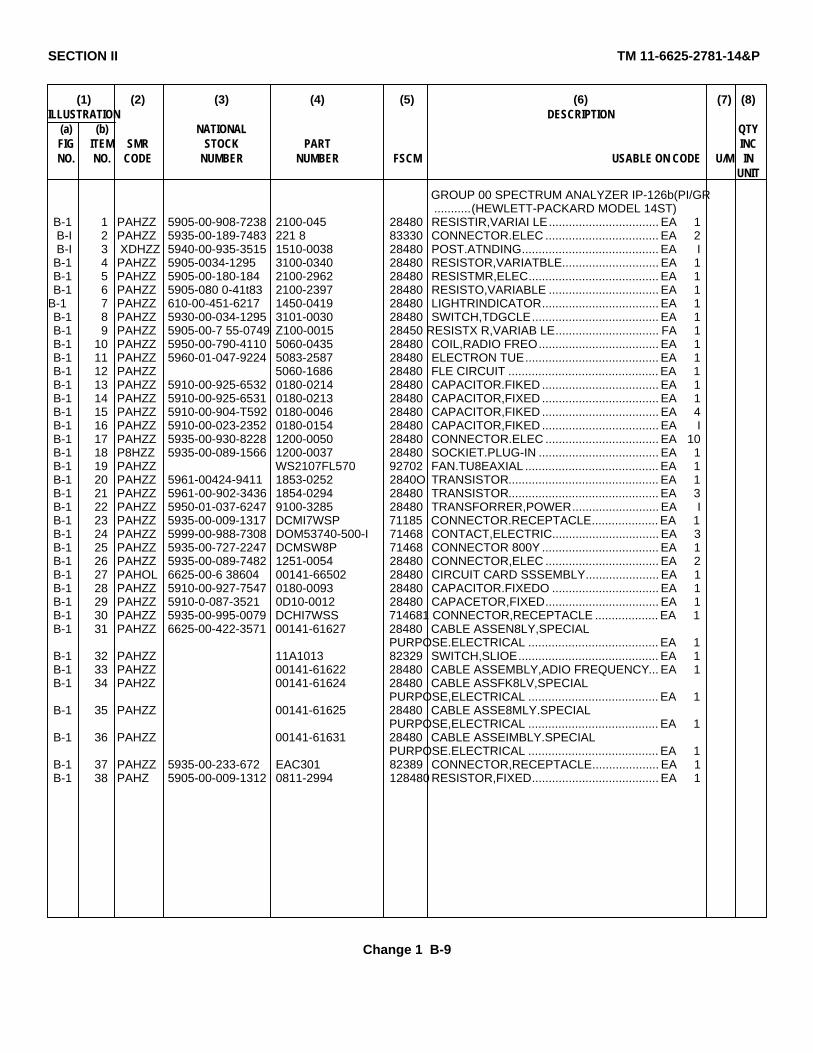
SECTION II TM 11-6625-2781-14&P
(1) (2) (3) (4) (5) (6) (7) (8)ILLUSTRATION DESCRIPTION
(a) (b) NATIONAL QTYFIG ITEM SMR STOCK PART INCNO. NO. CODE NUMBER NUMBER FSCM USABLE ON CODE U/M IN
UNIT
GROUP 00 SPECTRUM ANALYZER IP-126b(PI/GR...........(HEWLETT-PACKARD MODEL 14ST)
B-1 1 PAHZZ 5905-00-908-7238 2100-045 28480 RESISTIR,VARIAI LE................................. EA 1B-I 2 PAHZZ 5935-00-189-7483 221 8 83330 CONNECTOR.ELEC .................................. EA 2B-I 3 XDHZZ 5940-00-935-3515 1510-0038 28480 POST.ATNDING......................................... EA I
B-1 4 PAHZZ 5905-0034-1295 3100-0340 28480 RESISTOR,VARIATBLE............................. EA 1B-1 5 PAHZZ 5905-00-180-184 2100-2962 28480 RESISTMR,ELEC....................................... EA 1B-1 6 PAHZZ 5905-080 0-41t83 2100-2397 28480 RESISTO,VARIABLE ................................. EA 1
B-1 7 PAHZZ 610-00-451-6217 1450-0419 28480 LIGHTRINDICATOR................................... EA 1B-1 8 PAHZZ 5930-00-034-1295 3101-0030 28480 SWITCH,TDGCLE...................................... EA 1B-1 9 PAHZZ 5905-00-7 55-0749 Z100-0015 28450 RESISTX R,VARIAB LE............................... FA 1B-1 10 PAHZZ 5950-00-790-4110 5060-0435 28480 COIL,RADIO FREO.................................... EA 1B-1 11 PAHZZ 5960-01-047-9224 5083-2587 28480 ELECTRON TUE........................................ EA 1B-1 12 PAHZZ 5060-1686 28480 FLE CIRCUIT ............................................. EA 1B-1 13 PAHZZ 5910-00-925-6532 0180-0214 28480 CAPACITOR.FIKED ................................... EA 1B-1 14 PAHZZ 5910-00-925-6531 0180-0213 28480 CAPACITOR,FIXED ................................... EA 1B-1 15 PAHZZ 5910-00-904-T592 0180-0046 28480 CAPACITOR,FIKED ................................... EA 4B-1 16 PAHZZ 5910-00-023-2352 0180-0154 28480 CAPACITOR,FIKED ................................... EA IB-1 17 PAHZZ 5935-00-930-8228 1200-0050 28480 CONNECTOR.ELEC .................................. EA 10B-1 18 P8HZZ 5935-00-089-1566 1200-0037 28480 SOCKIET.PLUG-IN .................................... EA 1B-1 19 PAHZZ WS2107FL570 92702 FAN.TU8EAXIAL ........................................ EA 1B-1 20 PAHZZ 5961-00424-9411 1853-0252 2840O TRANSISTOR............................................. EA 1B-1 21 PAHZZ 5961-00-902-3436 1854-0294 28480 TRANSISTOR............................................. EA 3B-1 22 PAHZZ 5950-01-037-6247 9100-3285 28480 TRANSFORRER,POWER.......................... EA IB-1 23 PAHZZ 5935-00-009-1317 DCMI7WSP 71185 CONNECTOR.RECEPTACLE.................... EA 1B-1 24 PAHZZ 5999-00-988-7308 DOM53740-500-I 71468 CONTACT,ELECTRIC................................ EA 3B-1 25 PAHZZ 5935-00-727-2247 DCMSW8P 71468 CONNECTOR 800Y ................................... EA 1B-1 26 PAHZZ 5935-00-089-7482 1251-0054 28480 CONNECTOR,ELEC .................................. EA 2B-1 27 PAHOL 6625-00-6 38604 00141-66502 28480 CIRCUIT CARD SSSEMBLY...................... EA 1B-1 28 PAHZZ 5910-00-927-7547 0180-0093 28480 CAPACITOR.FIXEDO ................................ EA 1B-1 29 PAHZZ 5910-0-087-3521 0D10-0012 28480 CAPACETOR,FIXED.................................. EA 1B-1 30 PAHZZ 5935-00-995-0079 DCHI7WSS 714681 CONNECTOR,RECEPTACLE ................... EA 1B-1 31 PAHZZ 6625-00-422-3571 00141-61627 28480 CABLE ASSEN8LY,SPECIAL
PURPOSE.ELECTRICAL ....................................... EA 1B-1 32 PAHZZ 11A1013 82329 SWITCH,SLIOE.......................................... EA 1B-1 33 PAHZZ 00141-61622 28480 CABLE ASSEMBLY,ADIO FREQUENCY... EA 1B-1 34 PAH2Z 00141-61624 28480 CABLE ASSFK8LV,SPECIAL
PURPOSE,ELECTRICAL ....................................... EA 1B-1 35 PAHZZ 00141-61625 28480 CABLE ASSE8MLY.SPECIAL
PURPOSE,ELECTRICAL ....................................... EA 1B-1 36 PAHZZ 00141-61631 28480 CABLE ASSEIMBLY.SPECIAL
PURPOSE.ELECTRICAL ....................................... EA 1B-1 37 PAHZZ 5935-00-233-672 EAC301 82389 CONNECTOR,RECEPTACLE.................... EA 1B-1 38 PAHZ 5905-00-009-1312 0811-2994 128480 RESISTOR,FIXED...................................... EA 1
Change 1 B-9

SECTION II TM 11-6625-2781-14&P
(1) (2) (3) (4) (5) (6) (7) (8)ILLUSTRATION DESCRIPTION
(a) (b) NATIONAL QTYFIG ITEM SMR STOCK PART INCNO. NO. CODE NUMBER NUMBER FSCM USABLE ON CODE U/M IN
UNIT
B-1 39 PAHZZ 62113 06540 TERMINAL &OARD.................................... EA 1B-1 40 PAHZZ 5935-00-804-5144 31-221-1020 02660 CONNECTORIRECEPTACLE.................... EA 1B-1 41 PAHZZ 6150-01-027-5874 812-1530 28480 CABLE ASSEN8LY,POWER...................... EA 1B-1 42 PAHZZ 5999-00-995-1392 DN53742-S001 71468 CONTACT.ELECTRIC................................ EA 3B-1 43 PAHZZ 5935-00-275-7823 DCMNBS5 71468 CONNECTOR BODY ................................. EA 1B-1 44 PAHZZ 00141-61623 28480 CABLE ASSEMBLY.RAOD FREQUENCY. EA 1B-1 45 PAHZZ 6625-03-027-3660 5020-8122 28480 TERMINAL BOARD.................................... EA 1B-1 46 PAHZZ 5920-00-284-7466 NOX4 71400 FUSE.CARTRIDGE SELECT (120V) ......... EA 1B-1 46 PAHZZ 5920-01-033-4890 2110-0303 28480 FUSE,CARTRIDGE SELECT (220V) ......... EA 1
B- 1 47 PAHZZ 6625-00-435-4181 5060-0521 28480 CABLE ASSENMBLY,SPECIALPURPOSE.ELECTRICAL........................... EA 1
B-1 48 PAHZ 6625-00-450-7243 00141-61101 28480 HIGH VOLTAGE TRIPLER ASSEMBLY..... EA 1B-1 49 PAHDL 6625-00-45-9249 00141-66519 28480 CIRCUIT CARD ASSEMBLY...................... EA 1B-1 50 PAH22 5905-00-496-3412 0811-2030 28480 RESISTOR, FlXED..................................... EA 2B-1 51 PAHZZ 5940-00-177-9847 0360-0015 28480 TERMINAL 80ARD..................................... EA 2B-1 52 PAHZZ 5905-00-104-8330 RCR20G333JS 81349 RESISTMO,FIXEO ..................................... EA 1B-1 53 PAHDL 6625-00-439-1082 00141-66520 28480 CIRCUIT CARD ASSEMBLY...................... EA 1B-1 54 PAHDL 6625-00-439-1086 00141-66515 28480 CIRCUIT CARD ASSEMYBLY ................... EA 1B-1 55 PAHZZ 5961-00-229-6882 N3209 04713 SEHICONDUCTOR DEVICE.010DE.......... EA 2B-1 56 PAHZZ 5905-0-942-3530 0815-0031 28480 RESISTOI.PIXED ....................................... EA 1B-1 57 PAHZZ 5999-00-279-7999 104002 75915 CLIP.ELECTRICAL .................................... EA 3B-1 58 PAHDL 0960-0443 28480 CIRCUIT CARD ASSEMBLY (A7).............. EA 1B-1 59 PAHZZ 59300-92-6455 3103-0009 28480 SWITCH,THERMOSTAT............................ EA 1
Change 1 B-10/(B-11 Blank)

TM 11-6625-2781-14&P
Figure B-2. Circuit Card Assembly, Diode.
Change 1 B-12

SECTION II TM 11-6625-2781-14&P
(1) (2) (3) (4) (5) (6) (7) (8)ILLUSTRATION DESCRIPTION
(a) (b) NATIONAL QTYFIG ITEM SMR STOCK PART INCNO. NO. CODE NUMBER NUMBER FSCM USABLE ON CODE U/M IN
UNIT
GROUP 01 CIRCUIT CARD ASSEMBLY.DIWE.AL
B-2 1 XD0ZZ 59IO-00-797-4909 0150-0052 28480 CAPACITOR.FIXEO................................... EA 3B-2 2 XDOZZ 5961-00-951-1505 SR1358-9 04113 SEMICONDUCTOR.................................... EA 12
Change 1 B-13(B-14 Blank)

TM 11-6625-2781-14&P
Figure B-3. Circuit Card Assembly, Power Supply (Sheet 1 of 2).
Change 1 B-15
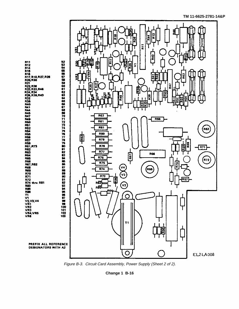
TM 11-6625-2781-14&P
Figure B-3. Circuit Card Assembly, Power Supply (Sheet 2 of 2).
Change 1 B-16

SECTION II TM 11-6625-2781-14&P
(1) (2) (3) (4) (5) (6) (7) (8)ILLUSTRATION DESCRIPTION
(a) (b) NATIONAL QTYFIG ITEM SMR STOCK PART INCNO. NO. CODE NUMBER NUMBER FSCM USABLE ON CODE U/M IN
UNIT
GROUP 02 CIRCUIT CARD ASSEMRLY,POWER SUPPLY,A2
B-3 1 XDDZZ 5910-00-917-0668 192P10492PTS 56289 CAPACITOR,FIXED EA 4B-3 2 XDDZZ 15OD475K903582DY CAPACITOR.FIED,ELECTROLYTIC EA 2
S 56189B-3 3 XODZZ 5910-00-797-4909 0150-0052 28480 CAPACITOR,FIXED EA 2B-3 4 XDDZZ 5910-00-961-9591 192P47292PTS 56289 CAPACITOR,FIXED EA 1B-3 5 XDDZZ 1500476I 9035520Y CAPACITOR,FIXED.ELECTROLYTIC EA 1
S 56289B-3 6 PADZZ 5910-00-067-8305 0180-0138 28480 CAPACITOR,FIXEO EA 1B-3 7 XDDZZ 150D0105XOOSA2DY CAPACITOR.FIXED,ELECTROLYTIC EA 1
S 56289B-3 XDDZZ 5910-00-985-1261 0163-0151 23480 CAPACITOR.FIXED EA 5B-3 9 XDD2Z 5910-00-931-0029 0160-0907 284680 CAPACITOR,FIXEO EA 2B-3 10 XDDZZ 5910-00-444-0589 0160-0407 28480 CAPACITOR,FIXED EA 1B-3 11 XDOZZ S131-050-651-104 CAPACITOR,FIXED,CERAMIC
Z DIELECTRIC EA 1B-3 12 XDDZZ 5961-00-92-7939 FDG1088 34148 SEMICONDUCTOR EA 9B-3 13 XDDZZ 5961-00-904-0296 1901-0096 28480 SEMICONDUCTOR EA 1B-3 14 XDDZZ 5961-00-954-9182 1910-0016 28460 SEMICONDUWCTOR EA 2B-3 15 XDDZZ 5961-00-060-8638 SR1358-8 04713 SEAICONDUCTOR EA 2B-3 16 XDDZZ FD2387 07263 SEMICONDUCTOR DEVICE.OIODE EA 1B-3 17 XDDZZ 5961-0-917-9637 1912-0006 286480 SEMICONDUCTOR EA 1B-3 18 XDDZZ 5961-00-911-9275 1901-0049 28480 SEMICONDUCTOR EA 1B-3 19 XDDZZ 5961-0-L106622 1901-0341 28480 SEMICONDUCTOR EA 2B-3 20 XDDZZ 5961-0-9205302 1901-0436 28480 SEMICONDUCTOR EA 2B-3 21 XDDZZ 5961-00-950-0531 1901-0029 28480 SEMICONDUCTOR EA 1B-3 22 XDDZZ 5920-00-556-9946 2110-0067 28480 FUSE.CARTRIDGE EA 1B-3 23 XDDZZ 5920-00-254-9494 3L12-750 75915 FUSE,CARTRIOGE EA 1B-3 24 XDDZZ 312-500 75915 FUSE.CARTRIODGE EA 1B-3 25 XDDZZ 5920-00-O1-6652 312003 759151 FUSE,CARTRIDGE EA 1B-3 26 XDDZZ 5950-00-910-9938 0490-0191 24801 COIL EA 1B-3 27 XDDZZ 5930-00-483-4003 0490-019 28460 SWITCN.REED EA 1B-3 28 XDDZZ 5950-00-946630 9140-0171 28460 COIL RADIO FREQUENCY EA 1B-3 29 XDZZ 5950-O-073-9426 1537-16 71895 COIL.RADIO FREQUENCY EA 1B-3 30 XDDZZ 5999-00-333-9620 2110-0269 26460 CLIP,ELECIRTCAL EA 8B-3 31 XDDZZ 5961-00-866-4810 2N708 80131 TRANSISTOR EA 1B-3 31 XDDZZ 5961-0-931-0372 2N3906 80131 TRANSISTOR EA 1B-3 32 XDD2Z 5961-0-917-0660 1854-0022 26480 TRANSISTOR EA 2B-3 34 XDDZZ 5961-00-937-3768 2N3417 80131 TRANSISTOR EA 1B-3 35 XDDZZ 5961-00-137-4608 1854-0071 28460 TRANSISTOR EA 4B-3 36 XDDZZ 5961-0-985-9073 2N3053 80131 TRANSISTOR EA 1
Change 1 B-17

SECTION II TM 11-6625-2781-14&P
(1) (2) (3) (4) (5) (6) (7) (8)ILLUSTRATION DESCRIPTION
(a) (b) NATIONAL QTYFIG ITEM SMR STOCK PART INCNO. NO. CODE NUMBER NUMBER FSCM USABLE ON CODE U/M IN
UNIT
B-3 37 XDDZZ 5961-00-892-8706 2N3I904 80131 TRANSISTOR EA 1B-3 38 XDDZZ 5961-00-988-3608 2N964 80131 TRANSISTOR EA 1B-3 39 XDDZZ 5961-00-410-8882 2N4918 04713 TRANSISTOR EA 1B-3 40 XDDZZ 5961-00-987-4700 1853-0034 28480 TOTANSISTOR EA 1B-3 41 XDDZZ 5961-00-137-0999 1855-0057 28480 TRANSISTOR EA 1B-3 42 XDDZZ 5905-00-192-3987 E81041 01121 RESISTOR,FIKED,CONP EA 1B-3 43 XDDZZ 5905-00-056-0446 0764-0033 28480 RESISTOR.FIKED EA 1B-3 44 XDDZZ 5905-00-917-5670 0761-0007 28480 RESISTOR,FIXED EA 1B-3 45 XDDZZ 5905-00-194-7894 CBZ1021 01121 RESISTOR,FIXED EA 5B-3 46 XDDZZ 5905-00-102-5294 CB1015 01121 RESISTOR.FIXED EA 1B-3 47 XDDZZ 5905-00-931-9908 0757-0044 28480 RESISTOR,FXED EA 2B-3 48 XDDZZ 5905-00-981-7529 0757-0401 2S480 RESISTOR.FIXTEO EA 2B-3 49 XDDZZ 5905-00-193-4294 0757-0273 28480 RESISTOR,FIXEO EA 2B-3 50 XDDZZ 5905-00-904-4412 0757-0465 28480 RESISTOR.FIKTD EA 2B-3 51 XDDZZ 5905-00-920-5301 0757-0370 28480 RESISTOR,FIKED EA 2B-3 52 XDDZZ 5905-00-928-1025 2100-1589 28480 RESISTOR,VARIABLE EA 1B-3 53 XDDZZ 5905-00-930-796 0757-0367 28480 RESISTOR.FIXEO EA 1B-3 54 XDDZZ 5905-00-494-5081 0766-0033 28480 RESISTO.FIKED EA 1B-3 55 XDDZZ 5905-00-998-1793 0757-0434 28480 RESISTOR.FIXED EA 1B-3 56 XDDZZ 5905-00-998-1800 0761-0006 28480 RESISTOR.FIXED EA 1B-3 57 XDDZZ 5905-00-752-7345 E85631 01121 RESISTOR.FIXED EA 4B-3 58 XDDZZ 5905-00-929-7774 01757-0399 28480 RESISTOR.FIXED EA 2B-3 59 XDDZZ 5905-00-141-0744 RCR7G562JS5 81349 RESISTOR.FIXED EA 1B-3 60 XDDZZ 0757-0764 28480 RESISTOR,FIXED FILM EA 1B-3 61 XDDZZ 5905-00-929-2525 0757-0388 28480 RESISTOR,FIXED EA 3B-3 62 XDDZZ 5905-00-855-6792 0757-0436 28480 RESISTOR,FIXED EA 2B-3 63 XDDZZ 5905-00-927-2881 01757-0846 28480 RESISTOR.FIXED EA 3B-3 64 XDDZZ 5905-00-927-2878 0757-0772 28480 RESISTOR,FIXED EA 1B-3 65 XDDZZ 5905-00-909-3427 0727-0431 28480 RESISTOR,FIXED EA 1B-3 66 XDDZZ 5905-00-141-1168 RCR20G222JS 81349 RESISTOR.FIXEDO EA 1B-3 67 XDD2Z 5905-00-141-0596 RCR20G473JS 81349 RTESISTOR.FIKED EA 1B-3 68 XDDZZ 5905-00-917-0575 075T-0190 28480 RESISTOR,FIKED EA 1B-3 69 XDDZZ 5905-00-056-0426 0757-0480 28480 RESISTOR,FIXFD EA 1B-3 70 XDDZZ 5905-00-927-8507 2100-1588 28480 RESISTOR.VARIA8LE EA 1B-3 71 XDDZZ 5905-00-444-6291 0811-1746 28480 RESISTOR.FIXEO,WIRE WOUND EA 1B-3 72 XDDZZ 5905-00-891-4219 0757-0421 28480 RESISTOR,FIKED EA 1B-3 73 XDDZZ 5905-00-998-1794 0757-0428 28480 RESISTOR,FIXED EA 1B-3 74 XDDZZ 0761-0075 28480 RESISTOR,FIXEO,FILM EA 1B-3 75 XDDZZ 5905-00-920-5295 0698-3555 28480 RESISTOR,FIXED EA 1B-3 76 XDDZZ 5905-00-975-7140 0698-3554 28480 RESISTOR,FIKED.FILN EA 1
Change 1 B-18

SECTION II TM 11-6625-2781-14&P
(1) (2) (3) (4) (5) (6) (7) (8)ILLUSTRATION DESCRIPTION
(a) (b) NATIONAL QTYFIG ITEM SMR STOCK PART INCNO. NO. CODE NUMBER NUMBER FSCM USABLE ON CODE U/M IN
UNIT
B-3 77 XDDZZ 5905-00-726-6436 C83331 01121 RESISTOR,FIXEO EA 1B-3 78 XDDZZ 5905-00-917-6S89 0758-0054 28480 RESISTOR,FIXED EA 1B-3 79 XDDZZ 5905-00-410-7871 C81241 01121 RESISTOR,FIKED EA 1B-3 80 XDDZZ 0727-0845 28480 REISISTOR,FIXED.FILM EA 2B-3 81 XDOZZ 5905-00-444-6307 0721-0269 28480 RESISTORI.FIXEO EA 1B-3 82 XDDZZ 5905-00-802-4360 2100-0096 28480 RESISTOR,VARIABLE EA 1B-3 83 XDDZZ 5905-00-904-5689 CB1535 01121 RESISTOR.FIKED EA 1B-3 84 XDOZZ 5905-00-175-8651 2100-2108 28480 RESISTOR,VARIABLE EA 1B-3 85 XDDZZ 5905-00-549-5067 0698-6666 28480 RESISOR.,FIXED EA 1B-3 86 XDD2Z 5905-00-269-2629 0757-0344 28480 RESISTOR.FIXED EA 2B-3 87 XDDZZ 0761-0004 28480 RESISTOR,FIXEOD.FILM EA 1B-3 88 XDDZZ 5905-00-931-9909 0757-0832 28480 RESISTOR,FIXED EA 2B-3 89 XDDZZ 5905-00-056-0448 0757-0768 28480 RIES1ISTOR.FIXED EA 1B-3 90 XDDZZ 5905-00-891-2811 0157-0454 28480 RESISTOR,FIXED EA 1B-3 91 XDDZZ 5905-00-171-5956 2100-0095 28480 RESISTOR,VARIABLE EA 1B-3 92 XDDZZ 5905-00-920-5289 0698-3553 28480 RESISTOR,FIKED EA 8B-3 93 XDDZZ 5905-00-056-0552 07T1-0452 28480 IIESISTDR.FIXEDO EA 1B-3 94 XDDZZ 5905-00-105-7764 RCR07G222JS 81349 RESISTOR.FIXED EA 1B-3 95 XDOZZ 0698-6Z86 28480 RESISTOR, FlXED COMPOSITION EA 1B-3 96 XDDZZ 5950-00-180-4179 00141-61102 28480 TRANSFORNER,ELEC EA 1B-3 97 XDDZZ 5960-00-167-7875 1940-0013 28480 ELECTIRONTUBE EA 1B-3 98 XDDZZ 2190-0014 28480 LAMP.GLOW EA 3B-3 99 XDDZZ 5961-00-089-1038 1902-3402 28480 SENICNONUCTOR EA 1B-3 100 XDDZZ 5961-00-904-0295 1902-0034 28480 SEMICONDUCTOR EA 1B-3 101 XDDZZ 5961-00-995-2310 1932-3104 28480 SEPICONDUCTOR EA 1B-3 102 XDDZZ 5961-00-928-3159 1902-3385 28480 SEMICONOUCTOR EA 2B-3 103 XDDZZ 5961-00-904-0297 1902-0064 28480 SEMICONOUCTOR EA I1
Change 1 B-19

TM 11-6625-2781-14&P
Figure B-4. Circuit Card Assembly, Pulse.
Change 1 B-20

SECTION II TM 11-6625-2781-14&P
(1) (2) (3) (4) (5) (6) (7) (8)ILLUSTRATION DESCRIPTION
(a) (b) NATIONAL QTYFIG ITEM SMR STOCK PART INCNO. NO. CODE NUMBER NUMBER FSCM USABLE ON CODE U/M IN
UNIT
B-4 1 DDZZ 5910-00-497-7598 192P56292PTS 56289 CAPACITOR,FIXED EA 1B-4 2 XDDZZ 5910-00-009-3195 0160-2212 28480 CAPACITOR,FIXED EA 1B-4 3 XODZZ 5910-00-406-9675 0160-2307 28480 CAPACITOR.FIXED EA 1B-4 4 KDDZZ 5910-00-940-3184 0140-0207 28480 CAPACITOR.FIXED EA 1B-4 5 XDDZZ 5110-00-965-9728 192P10292PTS 56289 CAPACITOR,FIXED FA 1B-4 6 KDDZZ 301-OCOGCD0160J 72982 CAPACITOR.FIXED.CERANICDIELECTRIC EA 1B-4 7 DD2 5910-00-481-8507 0160-2146 28480 CAPACITOR,ELEC EA 1B-4 8 XODZZ 150226X9015820DY CAPACITOR.FIXED.ELECTROLYTIC EA 1
S 56289B-4 9 XDDZZ 150D474X90352DY CAPACITOR,FIXED,ELECTROLYTIC EA 1
S 56289B-4 10 XDDZZ 5910-00-917-0668 192P10492PTS 56289 CAPACITOR.FIXED EA 2B-4 11 XDDZZ 1500225X02042DY CAPACITOR.FIXED,ELECTROLYTIC EA 1
S 56289B-4 12 2DDZZ 5910-00-961-9591 192P47292PTS 56289 CAPACITOR,FIXED EA 1B-4 13 KDDZZ 5910-00-430-6016 0180-1735 28480 CAPACITOR.FIXED EA 2B-4 14 XDZ0Z 5961-00-797-4909 S0150-0052 28480 CAPACITOR,FIXED EA 1B-4 15 XDDZZ 5961-00-9Z8-7939 PFDGIOB 34148 SEMICONDUCTOR EA 23B-4 16 XDZZ 5961-00-821-0710 FD3369 34148 SENICONDUCTOR EA 3B-4 17 XDD1Z1 5961-00-951-1505 Sr1358-9 04713 SEMICONDUCTOR EA 1B-4 18 XDDZZ SR1846-1i2 04713 SEMICONOUCTOR EA 1B-4 19 KDDZZ 5950-00-431-3198 9100-1630 28480 COIL,ELECTRICAL EA 1B-4 20 XDOZZ 5961-00-904-254 1853-0020 28480 TRANSISTOR EA 1B-4 21 XDDZZ 5961-00-197-0252 4U4894 04713 TRANSISTOR EA 1B-4 22 XDDZZ 5961-00-137-4608 1854-0071 28480 TRANSISTOR EA 16B-4 23 XDDZ2 1854-0358 28480 TRANSISTOR EA 3B-4 24 XDDZZ 5961-00-942-4004 2N3440 80131 TRANSISTOR EA 1B-4 25 XDDZZ 5905-00-994-8480 0757-0473 28480 RESISTOR,FIXED EA 3B-4 26 XDZZ 5905-00-498-6044 C81051 01121 RESISTOR.FIXED EA 2B-4 27 DDZZ 5295-00-194-7894 C81021 01121 RESISTOR,FIXED EA 1B-4 28 XD02Z CR1811 01121 RESISTOR,FIXED.COMPOSITION EA 2B-4 29 X5D0Z 5905-00-105-7764 RCR07C222J5 81349 RESISTOR,FIXED EA 3B-4 30 XDOZZ 5905-00-141-0717 C84731 01121 RESISTOR,FIXED EA 1B-4 31 XDOZZ 5905-00-498-6053 C82231 01121 RESISTOR,FIXED EA 3B-4 32 XDDZZ 5905-00-917-6341 0698-3155 28480 RESISTOR.FIKED EA 1B-4 33 KDOZZ 5905-00-858-9207 0757-0430 28480 RESISTOR,FIXED EA 1B-4 34 KDDZZ 5905-00-918-7479 2100-0424 28480 RESISTOR NETWORK EA 1B-4 35 XDD2 5905-00-709-6996 0757-0469 28480 RESISTOR,FIXED EA 1B-4 36 XODZZ 5905-00-056-0447 0757-0481 28480 RESISTOR,FIXED EA 2B-4 37 XDDZZ 5905-00-189-6699 2100-0983 28480 RESISTOR,VARIABLE EA 1
Change 1 B-21

SECTION II TM 11-6625-2781-14&P
(1) (2) (3) (4) (5) (6) (7) (8)ILLUSTRATION DESCRIPTION
(a) (b) NATIONAL QTYFIG ITEM SMR STOCK PART INCNO. NO. CODE NUMBER NUMBER FSCM USABLE ON CODE U/M IN
UNIT
B-4 38 XDDZZ 5905-00-118-7906 0757-0466 28480 RESISTOR,FIXED EA 1B-4 39 XDDZZ 5905-00-498-6048 C81831 01121 RESISTOR,FIXED EA 1B-4 40 XDDZZ 5905-00-497-5613 C01061 01121 RESISTOR,FIXED EA 3B-4 41 XDDZZ 5905-00-990-6659 C84741 01121 RESISTOR,FIXED EA 2B-4 42 XDDZZ 5905-00-758-6915 0698-4009 28480 RESISTOR,FIXED EA 1B-4 43 XDDZZ 5905-00-857-0125 0757-0476 28480 RESISTOR,FIXFD EA 2B-4 44 XDDZZ 5905-00-877-5769 0757-0456 28480 RESISTOR,FIXED EA 1B-4 45 XDDZZ 5905-00-830-6715 0757-0128 28480 RESISTOT,FIXED EA 1B-4 46 XDDZZ 0757-0850 28480 RESISTOR,FIXED,FILM EA 1B-4 47 XDDZZ 5905-00-930-7956 0757-0367 28480 RESISTOR,FIXED EA 1B-4 48 XDDZZ 5905-00-105-7768 RCR0T7G56LJS 81349 RESISTOR.FIXED EA 1B-4 49 XDDZZ RCR07G6823JS 81349 RESISTOR,FIXED.FILM EA 1B-4 50 XDDZZ 5905-00-407-2152 C8224I1 01121 RESISTOR,FIXED EA 1B-4 51 XDDZZ 5905-00-755-2613 C81031 01121 RESISTOR,FIKED EA 4B-4 52 XDDZZ 5905-00-809-8029 C84721 0112L RESISTOR,FIXED EA 7B-4 53 XDDZZ 5905-00-560-0426 0757-0480 28480 RESISTOR,FIXED EA 28-4 54 XDDZZ 0757-0791 28480 RESISTOR,FIXED,FILM EA 1B-4 55 XDDZZ 5905-00-104-5819 0761-0083 28480 RESISTOR,FIXED EA 1B-4 56 XDDZZ 5905-00-110-0388 C81041 01121 RESISTOR,FIXED EA 5B-4 57 XDDZZ 5905-00-119-3504 RCR07G273JS 81349 RESISTOR.FIXED EA 1B-4 58 XDDZZ 5905-00-721-0131 C82211 01121 RESISTOR,FIXED EA 1B-4 59 XDDZZ C88231 01121 RESISTOR.FIXED.COMPOSITION EA 1B-4 60 XDDZZ 5905-00-221-8309 0698-3647 28480 RESISTOR,FIXED EA 1B-4 61 XDDZZ 5905-00-119-3505 RCR07G683JS 81349 RESISTOR.FIXED EA 2B-4 62 XDDZZ 5905-00-126-6683 C8332 01121 RESISTOR,FIKED EA 2B-R 63 XDDZZ 5005-00-111-1684 RCR07G155JS 813491 RESISTOR,FIKED EA 1B-4 64 XDDZZ 5905-00-913-9415 CR5635 01121 RESISTOR,FIXFD EA 1B-4 65 XDDZZ 5961-00-995-2310 1902-3104 28480 SEMICDNOUCTOR EA 1B-4 66 XDDZZ 5961-00-459-8636 1902-0597 28480 SEMICONDUCTOR EA 1
Change 1 B-22/(B-23 Blank)

TM 11-6625-2781-14&P
Figure B-5. Circuit Card Assembly, Horizontal Driver.
Change 1 B-24
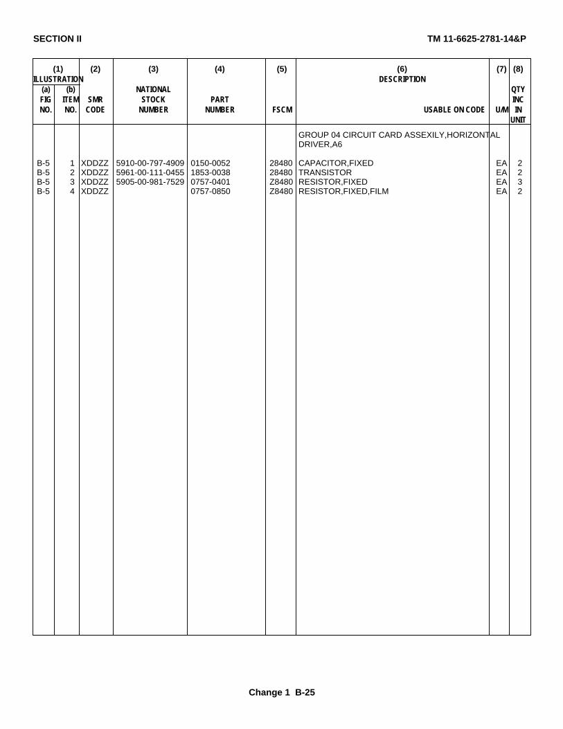
SECTION II TM 11-6625-2781-14&P
(1) (2) (3) (4) (5) (6) (7) (8)ILLUSTRATION DESCRIPTION
(a) (b) NATIONAL QTYFIG ITEM SMR STOCK PART INCNO. NO. CODE NUMBER NUMBER FSCM USABLE ON CODE U/M IN
UNIT
GROUP 04 CIRCUIT CARD ASSEXILY,HORIZONTALDRIVER,A6
B-5 1 XDDZZ 5910-00-797-4909 0150-0052 28480 CAPACITOR,FIXED EA 2B-5 2 XDDZZ 5961-00-111-0455 1853-0038 28480 TRANSISTOR EA 2B-5 3 XDDZZ 5905-00-981-7529 0757-0401 Z8480 RESISTOR,FIXED EA 3B-5 4 XDDZZ 0757-0850 Z8480 RESISTOR,FIXED,FILM EA 2
Change 1 B-25

SECTION IV TM 11-6625-2781-14&PNATIONAL STOCK NUMBER AND PART NUMBER INDEX
NOTE; LATEST NATIONAL STOCK NUMBER AND PART NUMBERT ASSIGNMENTS ARE INCLUDED AT END OF INDEXSTOCK NUMBER FIG. ITEM STOCK NUMBER FIG. ITEM
5930-00-008-7043 B-4 65 5905-00-944-5081 B-3 545905-00-009-1312 B-1 38 5905-00-496-3412 B-1 505935-00-009-1317 B-1 23 5905-00-497-5613 B-4 405910-00-009-3195 B-4 2 5910-00-497-7598 B-4 15920-00-010-6652 B-3 25 5905-00-498-6044 B-4 265910-00-023-2352 B-1 16 5905-00-498-6048 B-4 395930-00-034-1295 B-1 8 5905-00-498-6053 B-4 315905-00-056-0426 B-3 69 5920-00-556-9946 B-3 225905-00-056-0426 B-4 53 6625-00-613-8604 B-1 275905-00-056-0446 B-3 43 5905-00-709-6996 B-4 355905-00-056-0447 B-4 36 5905-00-721-0131 B-4 585905-00-056-0448 B-3 89 5905-00-726-6436 B-3 775905-00-056-0552 B-3 93 5935-00-727-2247 B-1 255961-00-060-8638 B-3 15 5905-00-752-7345 B-3 575910-00-067-8305 B-3 6 5905-00-755-0749 B-4 95950-00-073-9426 B-3 29 5905-00-755-2613 B-4 515910-00-007-3521 B-1 29 5905-00-758-6975 B-4 425961-00-089-1038 B-3 99 5905-00-711-5956 B-3 915935-00-069-1566 B-1 18 5950-00-190-4110 B-1 105935-00-089-7482 B-1 26 5910-00-197-4909 B-2 15935-00-089-7483 B-1 2 5910-00-797-4909 B-3 35905-00-102-5294 B-3 46 5910-00-797-4909 B-4 145905-00-104-5819 B-4 55 5910-00-797-4909 B-5 15905-00-104-8330 B-1 52 5935-00-804-5144 B-1 405961-00-105-6622 B-3 19 5905-00-809-8029 B-4 525905-00-105-7764 B-3 94 5961-00-821-0710 B-4 165905-00-105-7764 B-4 29 5905-00-830-6715 B-4 455905-00-105-7768 B-4 48 5905-00-657-0125 B-3 435905-00-110-0388 B-4 56 5905-00-858-6792 B-3 625961-00-111-0455 B-5 7 5905-00-858-9207 B-4 335905-00-111-1684 B-4 63 5961-00-866-48L0 B-3 315905-00-118-7906 B-4 38 5905-00-877-5769 B-4 445905-00-119-3504 B-4 57 5905-00-882-4360 B-3 825905-00-119-3505 B-4 61 5905-00-891-2811 B-3 905905-00-126-6683 B-4 62 5905-00-891-4219 B-3 725905-00-137-0999 B-3 41 5961-00-802-8706 B-3 375961-00-137-4608 B-3 35 5961-00-902-3436 B-1 215961-00-137-4608 B-4 22 5961-00-904-0295 B-3 1005905-00-141-0596 B-3 67 5961-00-904-0296 B-3 135905-00-141-0717 B-4 30 5S61-00-904-0297 B-3 1035905-00-141-0744 B-3 59 5961-00-904-2540 B-4 205905-00-141-1168 B-3 66 5905-00-904-4412 B-3 505960-00-167-7875 B-3 97 5905-00-904-5689 B-3 835905-00-175-8651 B-3 84 5905-00-908-7238 B-1 15940-00-177-9847 B-1 51 5905-00-908-7242 B-1 45953-00-180-4179 B-3 96 5905-00-909-3427 B-3 655905-00-180-4183 B-1 6 5950-00-910-9938 B-3 265905-00-180-4184 B-1 5 5960-00-911-9275 B-3 185905-00-189-6699 B-4 37 5905-00-913-9415 B-4 645905-00-192-3987 B-3 42 5905-00-917-0575 B-3 685905-00-193-4294 B-3 49 5961-00-917-0660 B-3 335905-00-194-7894 B-3 45 5910-00-917-0668 B-3 15905-00-194-7894 B-4 27 5910-00-917-0668 B-4 105961-00-197-0252 B-4 21 5905-00-917-5670 B-3 445905-00-221-8309 B-4 60 5905-00-917-6889 B-3 785961-00-221-6882 B-1 55 5961-00-917-9637 B-3 175935-00-233-6728 B-1 37 5905-00-918-7479 B-4 345905-00-269-2629 B-3 86 5905-00-920-5289 B-3 925935-00-215-7823 B-1 43 5905-00-920-5295 B-3 755999-00-219-7999 B-1 57 5905-00-920-5301 B-3 515120-00-284-7466 B-1 46 5961-00-920-5302 B-3 205920-00-84-9494 B-3 23 5930-00-925-6455 B-1 595999-00-333-9620 B-3 30 5910-00-925-6531 B-1 145910-00-406-9675 B-4 3 5910-00-925-6532 B-1 135905-00-407-2152 B-4 50 5905-00-927-2878 B-3 645905-00-410-7872 B-3 79 5905-00-927-2681 B-3 635961-00-410-8882 B-3 39 5910-00-927-7547 B-1 285961-00-424-9411 B-1 20 5905-00-927-8507 B-3 705910-00-430-6016 B-4 13 5905-00-928-1025 B-3 525950-00-431-3198 B-4 19 5961-00-928-3159 B-3 1026625-00-439-1086 B-1 54 5961-00-928-7939 B-3 125910-00-444-0589 B-3 10 5961-00-928-7939 B-4 155905-00-444-L291 B-3 71 5905-00-929-2528 B-3 615905-00-444-6307 B-3 81 5905-00-929-7774 B-3 586625-00-450-7243 B-1 48 5905-00-930-7956 B-3 536625-00-452-9249 B-1 49 5905-00-930-7956 B-4 475961-00-459-8636 B-4 67 5935-00-930-8228 B-1 175010-00-481-6507 B-4 7 5910-00-931-0329 B-3 95930-00-463-4003 B-3 27 5961-00-931-0372 B-3 325905-00-494-5067 B-3 85 5905-00-931-9908 B-3 47
Change 1 B-26

SECTION IV TM 11-6625-2781-14&PNATIONAL STOCK NUMBER AND PART NUMBER INDEX
STOCK NUMBER FIGURE ITEM STOCK NUMBER FIGURE ITEMNO. NO. NO.
5905-00-937-9909 B-3 88 5905-00-981-7529 B-5 35940-00-935-3515 B-7 3 5910-00-984-7592 B-1 155961-00-937-3768 B-3 34 5910-00-985-1261 B-3 85910-00-940-3184 B-4 4 5961-00-985-9073 B-3 365905-00-942-3533 B-1 56 5961-00-987-4700 B-3 405961-00-942-4004 B-4 24 5999-00-988-7308 B-1 245950-00-943-6630 B-3 28 5961-00-989-3608 B-3 385961-00-950-0537 B-3 21 5905-00-990-6659 B-4 415961-00-951-1505 B-2 2 5905-00-994-6460 B-4 255961-00-951-1505 B-4 11 5935-00-995-0079 B-1 305961-00-954-9182 B-3 14 5999-00-995-1392 B-1 425910-00-961-9591 B-3 4 5961-00-995-2310 B-3 1015910-00-961-1591 B-4 12 5961-00-995-2310 B-4 665910-00-965-9728 B-4 5 5905-00-998-1793 B-3 555905-00-975-7140 B-3 76 5905-00-998-1794 B-3 735905-00-916-3418 B-4 32 5905-00-998-1800 B-3 565905-00-981-7529 B-3 48 5950-01-037-6247 B-1 22
Part Fig. Item. Part Fig. Item
Number FSCM No. No. Number FSCM No. No.
CB1015 01121 B-3 46 00141-61627 28480 B-1 31CB1021 01121 B-3 45 0O141-61631 28480 B-1 36CB1021 01121 B-4 27 00141-66502 28480 B-1 21CB1031 01121 B-4 51 00141-66515 28480 B-1 54CB1041 01121 B-4 56 00141-66519 28480 B-1I 49CB1051 01121 B-4 26 00141-66520 28480 B-1 53CB1061 01121 B-4 40 0140-0207 28480 B-4 4CB1241 01121 B-3 19 0150-0052 28480 B-2 1CB1535 01121 B-3 83 0153-0052 28480 B-3 3CB1811 01121 B-4 28 0150-0052 28480 B-4 14CB1831 01121 B-4 39 0150-0052 28480 B-5 1CB2211 01121 B-4 58 O160-0151 28480 B-3 8CB2231 01121 B-4 31 O160-0407 28480 B-3 10CB2241 01121 B-4 50 0160-0907 28480 B-3 9CB3321 01121 B-4 62 0160-2146 28480 B-4 7CB3331 01121 B-3 17 0L60-2212 28480 B-4 2CB4771 01121 B-4 52 0160-2307 28480 B-4 3CB4173 01121 B-4 30 0180-0012 28480 B-1 29CB4741 01121 B-4 41 0180-0046 28480 B-1 15CB5635 01121 B-4 64 0180-0093 28480 B-1 28CB8231 01121 B -4 55 0180-0138 28480 B-3 6DCM17W5P 71785 B-1 23 0180-0154 28480 B-1 16DCMI17W5S 71468 B-1 30 0180-0213 28480 B-1 14DCM8W8P 71468 B-1 25 0180-0214 28480 B-1 13DCM8W8S 71468 B-1 43 0180-1735 28480 B-4 13DM53740-500-1 71468 B-1 24 0360-0015 28480 B-1 51DM53742-5001 71468 B-1 42 0490-0189 28480 B-3 27EAC3O0 82389 B-1 31 0490-0191 28480 B-3 26EB1041 01121 B-3 42 0690-3155 28480 B-4 32FB5631 01121 B-3 57 0698-3553 28480 B-3 92FDG1088 34148 B-3 12 0698-3554 28480 B-3 76FDG1088 34148 B-4 15 0698-3555 28480 B-3 75FD2387 07263 B-3 16 0698-3647 28480 B-4 60FD3369 34148 B-4 16 0698-4009 28480 B-4 42MDX4 71400 B-1 46 0698-6286 28480 B-3 95HU4894 04713 B-4 21 0698-6666 2848O B-3 85RCR07G155JS 81349 B-4 63 0727-0269 28480 B-3 81RCR07G2Z2JS 81349 B-3 94 0727-0431 28480 B-3 65RCR07G222JS 81349 B-4 2Y 0727-0845 28480 B-3 80RCR07G273JS 81349 B-4 57 0757-0044 28480 B-3 47RCR07GS61JS 81349 B-4 48 0757-0128 28480 B-4 45RCP07G562JS 81349 B-3 59 0751-0190 2848O B-3 68RCR07G683JS 81349 B-4 61 0757-0273 28480 B-3 49RCR07G823JS 81349 B-4 49 0757-0344 28480 B-3 86
Change 1 B-26

SECTION IV TM 11-6625-2781-14&PNATIONAL STOCK NUMBER AND PART NUMBER INDEX
Part Fig. Item. Part Fig. ItemNumber FSCM No. No. Number FSCM No. No.
RCR20G222JS 81349 B-3 66 0757-0361 28480 B-3 53RCR20G333J5 81349 B-1 52 0757-0367 28480 B-4 47RCR20G473JS 81349 B-3 67 0757-0370 28480 B-3 51SR1358-8 04713 B-3 15 0757-0388 28480 B-3 61SR1358-9 04713 B-2 2 0757-0399 28480 B-3 58SR135--9 04713 B-4 17 0757-0401 28480 B-3 46SR1846-12 04713 B-4 18 0757-0401 28480 B-5 3WS2107FL570 92702 B-1 19 0757-0421 28480 B-3 7200141-61101 28480 B-1 48 0757-0428 28480 B-3 7300141-61102 28480 B-3 96 0757-0430 28480 B-4 3300141-61622 28480 B-1 33 0757-0434 28480 B-3 5500141-61623 28480 B-1 44 0757-0436 28480 B-3 6200141-61624 28480 B-1 34 0757-0452 28480 B-3 9300141-61625 28480 B-1 35 0757-0454 26480 B-3 900757-0456 28480 B-4 44 1902-0064 28480 B-3 1030757-0465 28480 B-3 50 1902-0597 28480 B-4 670157-0466 28480 B-4 38 1902-3104 28480 B-3 1010751-0469 28480 B-4 35 1902-3104 28480 B-4 660757-0473 28480 B-4 25 1902-3385 28480 B-3 1020757-0476 28480 B-4 43 1902-3402 28480 B-3 990757-0480 28480 B-3 69 1910-0016 28480 B-3 140757-0480 28480 B-4 53 1912-0006 28480 B-3 170757-0481 28480 B-4 36 192P10292PTS 56289 B-4 50757-0764 284d0 B-3 60 192P10492PTS 56289 B-3 10757-0768 28480 B-3 89 192P10492PTS 56289 B-4 100757-0772 28480 B-3 64 192P47292PTS 56289 B-3 40757-0791 28480 B-4 54 192P47292PTS 56289 B-4 120757-0e39 28480 B-3 68 192P56292PTS 56289 B-4 10757-0846 28480 B-3 63 1940-0013 28480 B-3 970757-0850 28480 B-4 46 2N3053 80131 B-3 360757-0850 28480 B-5 4 2N3417 80131 B-3 340758-0054 28480 B-3 78 2N3440 80131 B-4 240761-0004 28480 B-3 87 2N3904 80131 B-3 370761-0006 28480 B-3 56 2N3906 80131 B-3 320761-0007 28480 B-3 44 2N4918 04713 B-3 390761-0075 28480 B-3 74 2N708 80131 B-3 310761-0083 28480 B-4 55 2N964 80131 B-3 380164-0033 28480 B-3 43 2100-0015 28480 B-1 90166-0033 28480 B-3 54 2100-0095 28480 B-3 910811-1746 28480 B-3 71 2100-0096 28480 B-3 820811-2033 28480 B-1 50 2100-0374 28480 B-1 40811-2994 28480 B-1 38 2100-0424 28480 B-4 340815-0031 28480 B-1 56 2100-0445 28480 B-1 11N3209 04713 B-1 55 2100-0983 28480 B-4 37104002 15915 B-1 51 2100-1588 26480 B-3 7011A1013 82329 B-1 32 2100-1589 28480 B-3 521200-0031 2840d B-1 18 2100-2108 28480 B-3 841200-0050 28480 B-1 17 2100-2897 28480 B-1 61251-0054 28480 B-1 26 2100-2962 28480 B-1 51450-0419 28480 B-1 7 2110-0067 28480 B-3 22150D105X0050A2DYS 56289 B-3 7 2110-0289 28480 B-3 30150D225X0020A2DYS 56289 B-4 11 2110-0303 28480 B-1 46150D226X001582DYS 56289 B-4 8 2190-0014 28480 B-3 98150D474X9015B2DYS 56289 B-4 9 221- 83330 B-1 2150D475X9035B2DYS 56289 B-3 2 301-000C0G0160J 72982 B-4 6150D476X9035S2DYS 56289 B-3 5 31-221-1020 02660 B-1 401510-0038 28480 B-1 3 3101-0033 28480 B-1 81537-76 71895 B-3 29 3131-1259 28480 B-4 651853-0020 28480 B-4 20 3103-0009 28480 B-1 591853-0034 28480 B-3 40 312-500 75915 B-3 241853-0038 28480 B-5 2 312-750 75915 B-3 231853-0252 28480 B-1 20 312-003 75915 B-3 251854-0022 28480 B-3 33 5020-8122 28480 B-1 451854-0071 28480 B-3 35 5060-0435 28480 B-1 101854-0071 28480 B-4 22 5060-3521 28430 B-1 471654-0294 28480 B-1 21 5060-1686 28480 B-1 12
Change 1 B-27

TM 11-6625-2781-14&P
Part Fig. Item. Part Fig. Item
Number FSCM No. No. Number FSCM No. No.
1854-0358 28480 B-4 23 5083-2587 26480 B-1 111855-0057 28480 B-3 41 628-13 06540 B-1 391901-0029 28480 B-3 21 8120-1538 28480 B-1 411901-0049 28480 B-3 18 8131-050-651-104Z 72982 B-3 111901-0096 28480 B-3 13 9100-1630 28480 B-4 191901-0341 28480 B-3 19 9100-3285 28460 B-1 221901-0436 2d480 B-3 20 9140-0171 28480 B-3 281902-0034 28480 B-3 100
LATEST NATIONAL STOCK NUMBER ASSIGMENTS LATEST PART NUMBER ASSIGNMENT
FIGURE ITEM FIGURE ITEMSTOCK NUMBER NO. NO. NO. NO.
6625-00-422-3571 B-1 31 0960-0443 28480 B-1 586625-00-435-4181 B-1 476625-00-439-1082 B-1 536210-00-451-6217 B-1 76625-01-027-3660 B-1 456150-01-027-5874 B-1 415920-01-033-4890 B-1 465960-01-047-9224 B-1 11
Change 1 B-28

TM 11-6625-2781-14&PAPPENDIX C
MAINTENANCE ALLOCATION
Section l. INTRODUCTION
C-1. GeneralThis appendix provides a summary of the maintenanceoperations for Spectrum Analyzer IP-1216(P)/GR(Hewlett-Packard Model 141T). It authorizes categoriesof maintenance for specific maintenance functions onrepairable items and components and the tools andequipment required to perform each function. Thisappendix may be used as an aid in planningmaintenance operations.
C-2. Maintenance Function
Maintenance functions will be limited to and defined asfollows:
a. Inspect. To determine the serviceability of an item by comparing its physical, mechanical, and/orelectrical characteristics with established standardsthrough examination.
b. Test. To verify serviceability and to detect incipient failure by measuring the mechanical or electricalcharacteristics of an item and comparing thosecharacteristics with prescribed standards.
c. Service. Operations required periodically tokeep an item in proper operating condition, i.., to clean(decontaminate), to preserve, to drain, to paint, or toreplenish fuel, lubricants, hydraulic fluids, or compressedair supplies.
d. Adjust. To maintain, within prescribed limits, bybringing into proper or exact position, or by setting theoperating characteristics to the specified parameters.
e. Align. To adjust specified variable elements ofan item to bring about optimum or desired performance.
f. Calibrate. To determine and cause corrections tobe made or to be adjusted on instruments or testmeasuring and diagnostic equipment’s used in precisionmeasurement. Consists of comparisons of two
instruments, one of which is a certified standard ofknown accuracy, to detect and adjust any discrepancy inthe accuracy of the instrument being compared.
g. Install. The act of emplacing, seating, or fixinginto position an item, part, module (component orassembly) in a manner to allow the proper functioning ofthe equipment or system.
h. Replace. The act of substituting a serviceablelike type part, subassembly, or module (component orassembly) for an unserviceable counterpart.
i. Repair. The application of maintenance services(inspect, test, service, adjust, align, calibrate, replace) orother maintenance actions (welding, grinding, riveting,straightening, facing, remachining, or resurfacing) torestore serviceability to an item by correcting specificdamage, fault, malfunction, or failure in a part,subassembly, module (component or assembly), enditem, or system.
j. Overhaul That maintenance effort(service/action) necessary to restore an item to acompletely serviceable/operational condition asprescribed by maintenance standards (i.e., DMWR) inappropriate technical publications. Overhaul is normallythe highest degree of maintenance performed by theArmy. Overhaul does not normally return an item to likenew condition.
i. Consists of those services/actions necessary for therestoration of unserviceable equipment to a like newcondition in accordance with original manufacturingstandards. Rebuild is the highest degree of materielmaintenance applied to Army equipment. The rebuildoperation includes the act of returning to zero those agemeasurements (hours, miles, etc.) considered inclassifying Army equipments/components.
C-1

TM 11-6625-2781-14&P
C-3. Column Entries
a. Column 1, Group Number. Column 1 lists groupnumbers, the purpose of which is to identify components,assemblies, subassemblies, and modules with the nexthigher assembly.
b. Column 2, Component/Assembly. Column 2contains the noun names of components, assemblies,subassemblies, and modules for which maintenance isauthorized.
c. Column 3, Maintenance Functions. Column 3lists the functions to be performed on the item listed incolumn 2. When items are listed without maintenancefunctions, it is solely for purpose of having the groupnumbers in the MAC and RPSTL coincide.
d. Column 4, Maintenance Category. Column 4specifies, by the listing of a "worktime" figure in theappropriate subcolumn(s), the lowest level ofmaintenance authorized to perform the function listed incolumn 3. This figure represents the active time requiredto perform that maintenance function at the indicatedcategory of maintenance. If the number or complexity ofthe tasks within the listed maintenance function vary atdifferent maintenance categories, appropriate "worktime"figures will be shown for each category. The number oftask-hours specified by the "worktime" figure representsthe average time required to restore an item (assembly,subassembly, component, module, end item or system)to a serviceable condition under typical field operatingconditions. This time includes preparation time,troubleshooting time, and quality assurance/ qualitycontrol time in addition to the time required to performthe specific tasks identified for the maintenancefunctions authorized in the maintenance allocation chart.Subcolumns of column 4 are as follows:
C - Operator/CrewO - OrganizationalF - Direct SupportH - General SupportD - Depot
e. Column 5, Tools and Equipment. Column 5specifies by code, those common tool sets (not individualtools) and special tools, test, and support equipmentrequired to perform the designated function.
f. Column 6, Remarks. (Not applicable).
C-4. Tool and Test Equipment Requirements
a. Tool or Test Equipment Reference Code. Thenumbers in this column coincide with the numbers usedin the tools and equipment column of the MAC. Thenumbers indicate the applicable tool or test equipmentfor the maintenance functions.
i. The codes in this column indicate the maintenancecategory allocated the tool or test equipment.
c. Nomenclature. This column lists the noun nameand nomenclature of the tools and test equipmentrequired to perform the maintenance functions.
d. National/NATO Stock Number. This column liststhe National/NATO stock number of the specific tool ortest equipment.
e. Tool Number. this column lists themanufacturer’s part number of the tool followed by theFederal Supply Code for manufacturers (5-digit) inparentheses.
C-5. Remarks (Sect. IV)
(Not applicable).
C-2

TM 11-6625-2781-14&PSECTION II MAINTENANCE ALLOCATION CHART
FOR
SPECTRUM ANALYZER IP-1216(P)/GR(HEWLETT-PACKARD MODEL 141T)
(1) (2) (3) (4) (5) (6)MAINTENANCE LEVEL
GROUP MAINTENANCE UNIT INTERMEDIATE DEPOT TOOLS ANDNUMBER COMPONENT ASSEMBLY FUNCTION C O F H D EQUIPMENT REMARKS
00 SPECTM ANALYZER P-1216(P)/GR Inspect 0.5 7(RLET-PACKARD MODEL 141T) Test 0.3 1 thru 7(NSN 662s-00-424-4370) Service 0.4 1 thru 7
Adjust 0.7 1 thru 7Repair 1.2 1 thru 7Overhaul 2.0 1 thru 7
01 CIRCUIT CARD ASSEMBLY DIODE, Al Inspect 0.3 7Replace .05 7Repair 0.5 1 thru 7
02 CIRCIT CARD ASSEWBLY POWER Inspect 0.3 7SUPPLY, A2 Replace 1.0 7
Repair 1.0 1 thru 7
03 CIRCUNIT CARD ASSEBLY, PULSE, A5 Inspect 0.3 7Replace 0.5 7Repair 0.5 1 thru 7
04 CIRCUIT CARD ASSEMBLY, Inspect 0.3 7HORIZORTAL DRIVER, A6 Replace 0.5 7
Repair 0.5 1 thru 7
Change 1 C-3

TM 11-6625-2781-14&P
SECTION III. TOOL AND TEST EQUIPMENT REQUIREMENTS FOR AN/GRC-240
(1) (2 ) (3) (4) (5)TOOL OR TEST
EQUIPMENT MAINTENANCE NATIONAL/NATO TOOLREF CODE LEVEL NOMENCLATURE STOCK NUMBER NUMBER
2 H, D VOLTMEE, ELECTRONIC AN/UM-15 6625-00-973-3986
3 H. D GENERATOR, SIGNAL AN/URM-127 6625-00-783-5965
4 H, D OSCILLOSCOPE, AN/USM-281C 6625-00-106-9622
5 H, D TRANSISTOR TEST SET TS-1836C/U 6625-00-159-2263
6 H, D WILTIMETER ME-26D/U 6625-00-913-9781
7 C, H, D TOOLS AND TEST EQUIPMNT USED BY THE TECHNICIAN FOR
ASSIGNED MISSION.
Change 1 C-4
SECTION III TM 11-6625-2781-14&P
TOOL AND TEST EQUIPMENT REQUIREMENTS FORSPECTRUM ANALYZER IP-1216(P)/GR
(1) (2 ) (3) (4) (5)TOOL OR TEST
EQUIPMENT MAINTENANCE NATIONAL/NATO TOOLREF CODE LEVEL NOMENCLATURE STOCK NUMBER NUMBER
1. H,D TEST SET, ELECTRICAL METER TS 682
2. H,D VOLTMETER, ELECTRONIC AN/UP-145 6625-00-973-3986
3. H,D GEERATOR, SIGNAL AN/URM-127 6625-00-783-5965
4. H,D OSCILLOSCOPR, AN/USM-281C 6625-00-106-9622
5. H,D TRANSISTOR TEST SET - TS 1836 C/u 6625-00-159-2263
6. R,D MULTIMRTER - ME 26 D/U 6625-00-913-9781
7. C,H,D TOOLS AND TEST EQUIPMETUSED BY THE REPAIRMA FORHIS/HER ASSIGNED MISSION.
C-5

TM 11-6625-2781-14&P
Figure 7-1. Component Identification Pulse Circuit A5

TM 11-6625-2781-14&P
Figure 7-2. Pulse Circuit Schematic
7-5

TM 11-6625-2781-14&P
Figure 7-3. Line Voltage Schematic
Figure 7-4. Option 009 Schematic Diagram
7-6

TM 11-6625-2781-14&P
Figure 8-6. Plug-in Jack Connections Figure 8-7. Auxiliary A and Auxiliary B Wiring Diagram
8-13

TM 11-6625-2781-14&P
Figure 8-8. Component Identification, Power Supply A2

TM 11-6625-2781-14&P
Figure 8-9. Component Identification, Diode Assy A1

TM 11-6625-2781-14&P
Figure 8-10. Low Voltage Schematic8-15
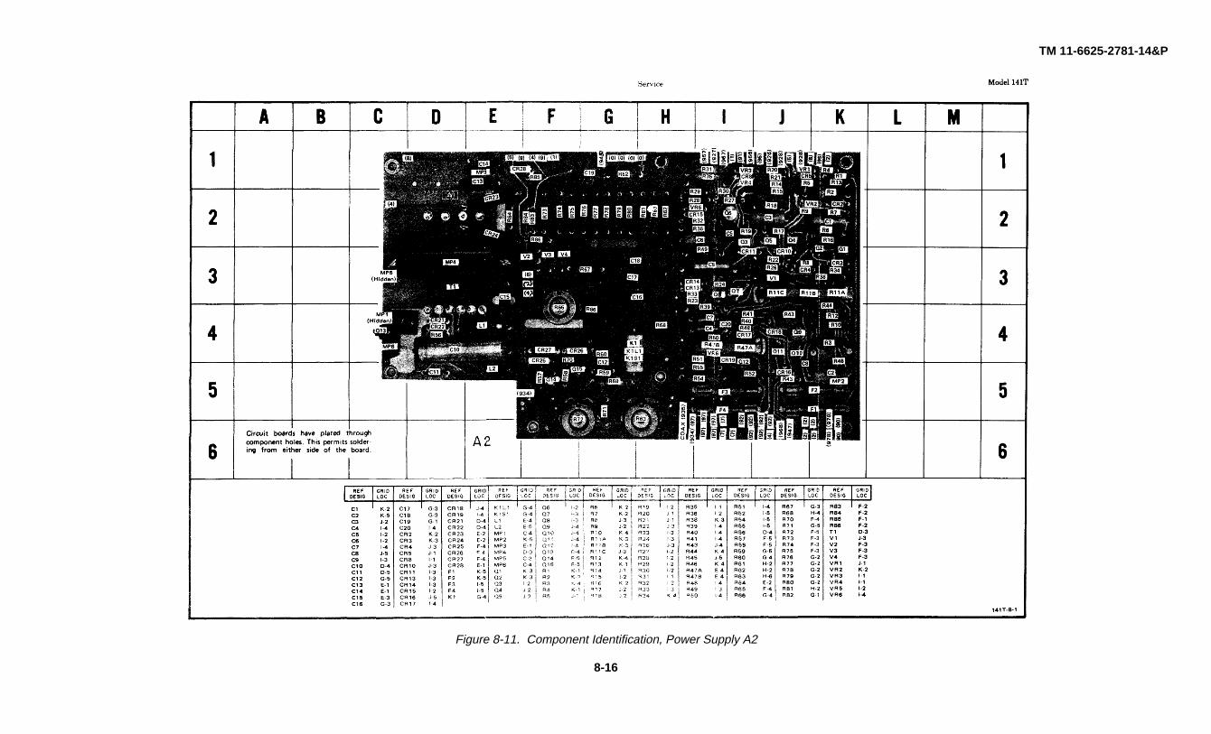
TM 11-6625-2781-14&P
Figure 8-11. Component Identification, Power Supply A2
8-16

TM 11-6625-2781-14&P
Figure 8-12. Component Identification, Horizontal Driver A6

TM 11-6625-2781-14&P
Figure 8-13. High Voltage Schematic8-17

TM 11-6625-2781-14&P
Figure 8-14. Component Identification, Pulse Circuit A58-18

TM 11-6625-2781-14&P
Figure 8-15. Waveforms
8-19

TM 11-6625-2781-14&P
Figure 8-16. Pulse Circuit Schematic
8-19

TM 11-6625-2781-14&PBy Order of the Secretary of the Army:
BERNARD W. ROGERSGeneral, United States Army
Official: Chief of StaffPAUL T. SMITH
Major General, United States ArmyThe Adjutant General
DISTRIBUTION:Active Army
TSG (1) WSMR (1)USAARENBD (1) Army Dep (1) exceptUSASA (2) Fort Carson (5)TRADOC (2) Fort Gillem (10)DARCOM (1) Fort Huachuca (5)TECOM (2) LBAD (10)OS Maj Comd (2) SAAD (30)USACC (2) TOAD (14)HISA (Ft Monmouth)(33) SHAD (3)Armies (1) USA Dep (1)USASIGS (10) Sig Sec USA Dep (2)Svc Colleges (1) Sig Dep (2)USAERDAA (1) Ft Richardson (ECOM Ofc)(1)USAERDAW (1) Sig FLDMS (1)
Units org under fol TOE: (1)29-13429-136
NG: None
USAR: None
For explanation of abbreviations used see, AR 310-50
*U.S. GOVERNMENT PRINTING OFFICE: 1993 - 343-421/61962


THE METRIC SYSTEM AND EQUIVALENTS

PIN: 032076-001