tm - radeon technologies groupradeon.com/wp-content/uploads/2016/08/polaris-tech-day... · under...
TRANSCRIPT

TM
Features, technologies and process
The Polaris Architecture

Under embargo until June 29, 2016 at 9 a.m. EST.TM
Best Graphics Core YetState-of-the-Art
Multimedia IPFuture-Proof
Monitor Support7 Cool & Quiet Gaming
Four Principles of the New Polaris Architecture
TM

Under embargo until June 29, 2016 at 9 a.m. EST.TM
1st Generation
DirectX® 11
OpenGL 4.2
OpenCL™ 1.2
EQAA
Partially Resident Textures (PRT)
Hardware Tessellation
MLAA
Updates Over Time:
DirectX® 11.1
DirectX® 12 FL 11_1
OpenGL™ 4.5
Mantle
Vulkan™
AMD LiquidVR™
Asynchronous Compute
Virtual Super Resolution
2nd Generation
Improved compute task scheduling (DirectX® 11)
Increased geometry throughput
AMD TrueAudio
OpenCL™ 1.2
OpenGL 4.3
HSA
Updates Over Time:
AMD FreeSync™
DirectX® 11.2
DirectX® 12 FL 12_0
OpenCL™ 2.0
OpenGL™ 4.5
AMD Mantle
Vulkan™
AMD LiquidVR™
Asynchronous Compute
Virtual Super Resolution
3rd Generation
High Bandwidth Memory support
Improved tessellation performance
Delta Color Compression (DCC)
Hardware scheduler (HWS) for asynchronous compute
Native FP16/Int16 shader ops (APU)
Data parallel processing instructions
4th Generation
Improved geometry processing
AMD LiquidVR™ technology for variable resolution rendering
DCC & updated memory controller
Shader instruction pre-fetch and enhanced buffering
Real-Time and prioritized asynccompute with spatial and temporal
scheduling
dGPU support for native FP16/Int16 Ops
AMD TrueAudio Next
H.265 Main10 decode acceleration
4K60 HEVC encode acceleration
HDMI® 2.0b
DisplayPort™ 1.3 HBR3
DisplayPort™ 1.4-HDR
HDR display support
TM
Under embargo until June 29, 2016 at 9 a.m. EST.TM
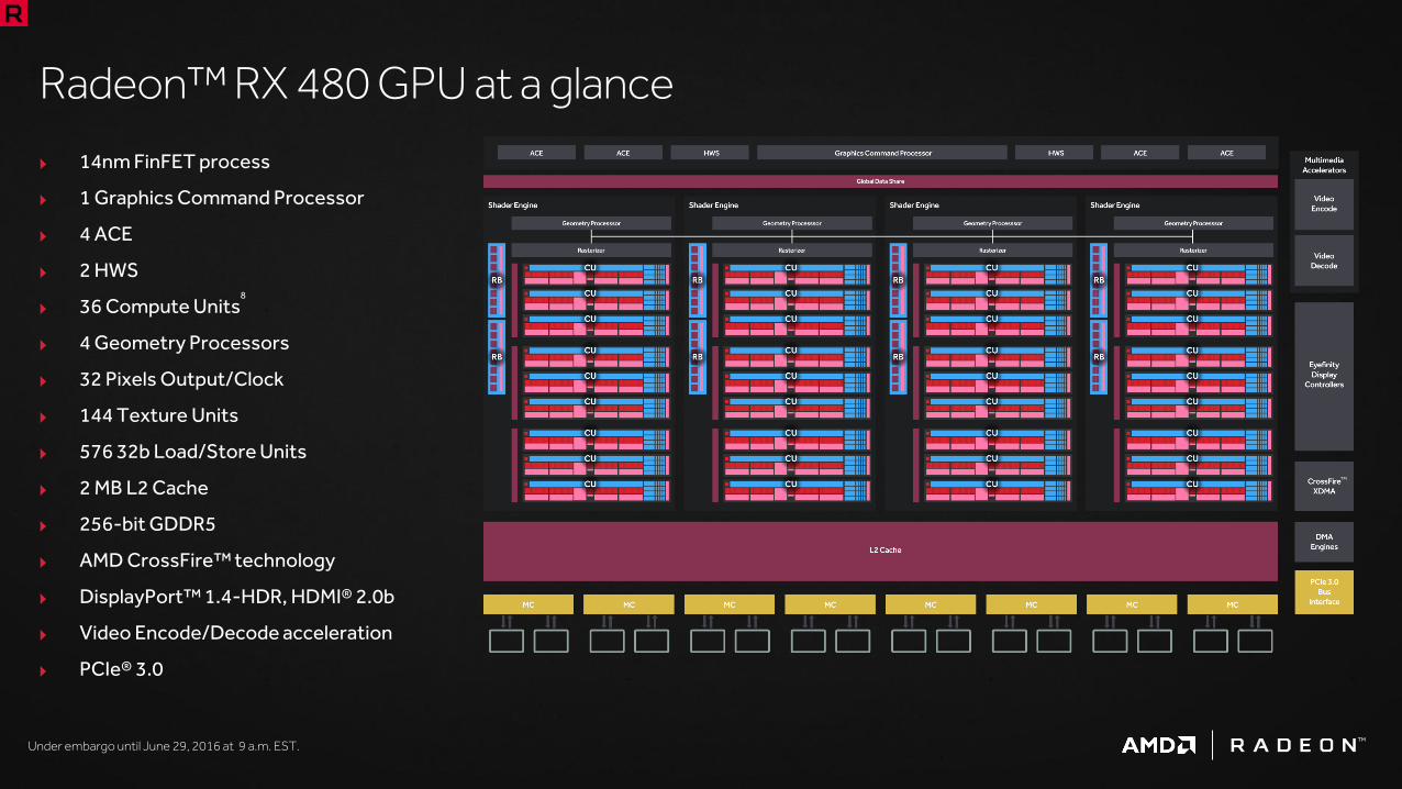
14nm FinFET process
1 Graphics Command Processor
4 ACE
2 HWS
36 Compute Units8
4 Geometry Processors
32 Pixels Output/Clock
144 Texture Units
576 32b Load/Store Units
2 MB L2 Cache
256-bit GDDR5
AMD CrossFire™ technology
DisplayPort™ 1.4-HDR, HDMI® 2.0b
Video Encode/Decode acceleration
PCIe® 3.0
Radeon™ RX 480 GPU at a glance
TM
Under embargo until June 29, 2016 at 9 a.m. EST.TM
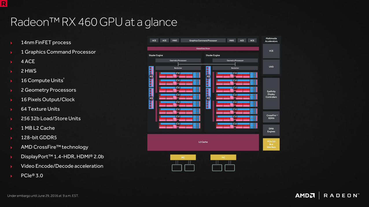
14nm FinFET process
1 Graphics Command Processor
4 ACE
2 HWS
16 Compute Units8
2 Geometry Processors
16 Pixels Output/Clock
64 Texture Units
256 32b Load/Store Units
1 MB L2 Cache
128-bit GDDR5
AMD CrossFire™ technology
DisplayPort™ 1.4-HDR, HDMI® 2.0b
Video Encode/Decode acceleration
PCIe® 3.0
Radeon™ RX 460 GPU at a glance
TM

Under embargo until June 29, 2016 at 9 a.m. EST.TM
4th-Gen GraphicsA Philosophy of Efficiency

Under embargo until June 29, 2016 at 9 a.m. EST.TM
Primitive Discard Accelerator
Culls triangles early in the pipeline with zero area or
no inclusive sample points
Returns grow as MSAA increases
New Index cache for small instanced geometry
Reduces data movement
Frees internal bandwidth resources
Maintains or improves primitive throughput during
instancing
Enhanced geometry engines
0%
50%
100%
150%
200%
250%
300%
350%
400%
Re
lati
ve
Pe
rfo
rman
ce
Tessellation With 4xAA3
Prim Discard Off Prim Discard On

Under embargo until June 29, 2016 at 9 a.m. EST.TM
Instruction prefetch
Improves efficiency by reducing pipeline stalls
Makes instruction caching more efficient
Increased per wave instruction buffer size
Improve single threaded performance
Tuned L2 cache behavior
Client cache request grouping
Improved cache and memory access efficiency
Native FP16 and Int16 support
Reduced memory/register footprint and bandwidth
Lower power execution
Graphics, computer vision, data learning
Improved shader efficiency
Branch & Message Unit
Scalar Unit
Vector Units(4x SIMD-16)
Vector Registers(4x 64KB)
Texture Filter Units (4)
Local Data Share(64KB)
L1 Cache(16KB)
SchedulerTexture Fetch
Load / Store Units (16)
Scalar Registers(4KB)
Polaris Architecture Compute Unit8

Under embargo until June 29, 2016 at 9 a.m. EST.TM
Improved shader efficiency
+15%PERFORMANCE PER CU
RADEON™ RX 480 VS. RADEON™ R9 2901
Instruction prefetch
Improves efficiency by reducing pipeline stalls
Makes instruction caching more efficient
Increased per wave instruction buffer size
Improve single threaded performance
Tuned L2 cache behavior
Client cache request grouping
Improved cache and memory access efficiency
Native FP16 and Int16 support
Reduced memory/register footprint and bandwidth
Lower power execution
Graphics, computer vision, data learning
UP TO

Under embargo until June 29, 2016 at 9 a.m. EST.TM
GPUOpen shader intrinsic functions
Direct access to inline ISA
Data parallel primitive access
Detect dynamically uniform conditions at runtime
Enables performance-critical functions
Execution exactly as developers intend
Available now: DirectX® 11, DirectX® 12 and Vulkan™
Console style programming enabled on PC to help extract more performance from the GPU
Console to PC

Under embargo until June 29, 2016 at 9 a.m. EST.TM
Updated memory controller & PHY
Supports up to 8Gbps GDDR5 memory devices
Up to 256GB/s memory bandwidth
Lossless DCC
Full 2/4/8 : 1 compression ratios supported
Driver optimized for utilization of DCC
Provides perf/bandwidth and power advantages
Extends the life, viability and efficiency of GDDR5
Efficient balance of resources
Yields higher peak bandwidth
Memory & delta color compression engines
0%
20%
40%
60%
80%
100%
120%
140%
160%
Radeon™ R9 290X Radeon™ R9 Fury X Radeon™ RX 480
Re
lati
ve M
em
ory
Ban
dw
idth
Peak Bandwidth Gain With DCC4
Uncompressible Data Compressible Data
Under embargo until June 29, 2016 at 9 a.m. EST.TM
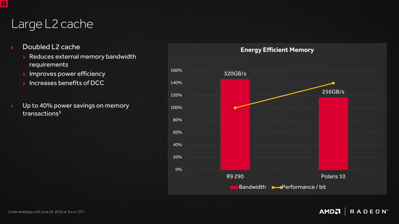
320GB/s
256GB/s
0%
20%
40%
60%
80%
100%
120%
140%
160%
R9 290 Polaris 10
Energy Efficient Memory
Bandwidth Performance / bit
Large L2 cache
Doubled L2 cache
Reduces external memory bandwidth requirements
Improves power efficiency
Increases benefits of DCC
Up to 40% power savings on memory transactions5
Under embargo until June 29, 2016 at 9 a.m. EST.TM
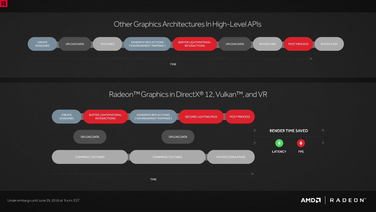
Other Graphics Architectures In High-Level APIs
Radeon™ Graphics in DirectX® 12, Vulkan™, and VR

Under embargo until June 29, 2016 at 9 a.m. EST.TM
* Diagrams for illustrative purposes only.
Sh
ade
r U
tiliz
ati
on
Time
Compute Preemption of Graphics Quick Response Queue
Graphics Compute
Asynchronous Compute
Radeon™ asynchronous compute is incredibly flexible

ACE ACE HWS GRAPHICS COMMAND PROCESSOR HWS ACE ACE
4
Hardware scheduler (HWS) for asynchronous compute
CPU kernel mode driver scheduling task offload
Real time and prioritized queues (audio/VR)
Temporal and spatial resource management
Concurrent task or process scheduling
Coordination and load balancing with graphics
Functionality can be updated with microcode

Under embargo until June 29, 2016 at 9 a.m. EST.TM
Polaris Architecture Summary
+15%PERFORMANCE PER CU
RADEON™ RX 480 VS. RADEON™ R9 2901
2.8xPERFORMANCE PER WATT
RADEON™ RX 470 VS. RADEON™ R9 270X2
FinFET 14 Technology | Micro–Architecture Tuned for Gaming | Physical Design Optimizations | DPM Techniques
UP TO UP TO

Under embargo until June 29, 2016 at 9 a.m. EST.TM
Future-Proof Display Support

Under embargo until June 29, 2016 at 9 a.m. EST.TM
DisplayPort™ 1.3 HBR3 and DisplayPort™ 1.4-HDR
Polaris is ready for DisplayPort™ 1.3 HBR3
Existing cables and connectors utilized
Up to 32.4Gbps of bandwidth
+80% bandwidth over HDMI® 2.0b
Polaris is ready for DisplayPort™ 1.4-HDR
Up to 10-bit 4K96
CTA-861.3 HDR metadata transport
Rec.2020 color space support
SMPTE 2084 EOTF
0
5
10
15
20
25
30
35
DisplayPort™ 1.1 DisplayPort™ 1.2 DisplayPort™ 1.3B
an
dw
idth
(Gb
ps)
Evolution of DisplayPort™ bandwidth across generations
Link Bandwidth
Under embargo until June 29, 2016 at 9 a.m. EST.TM
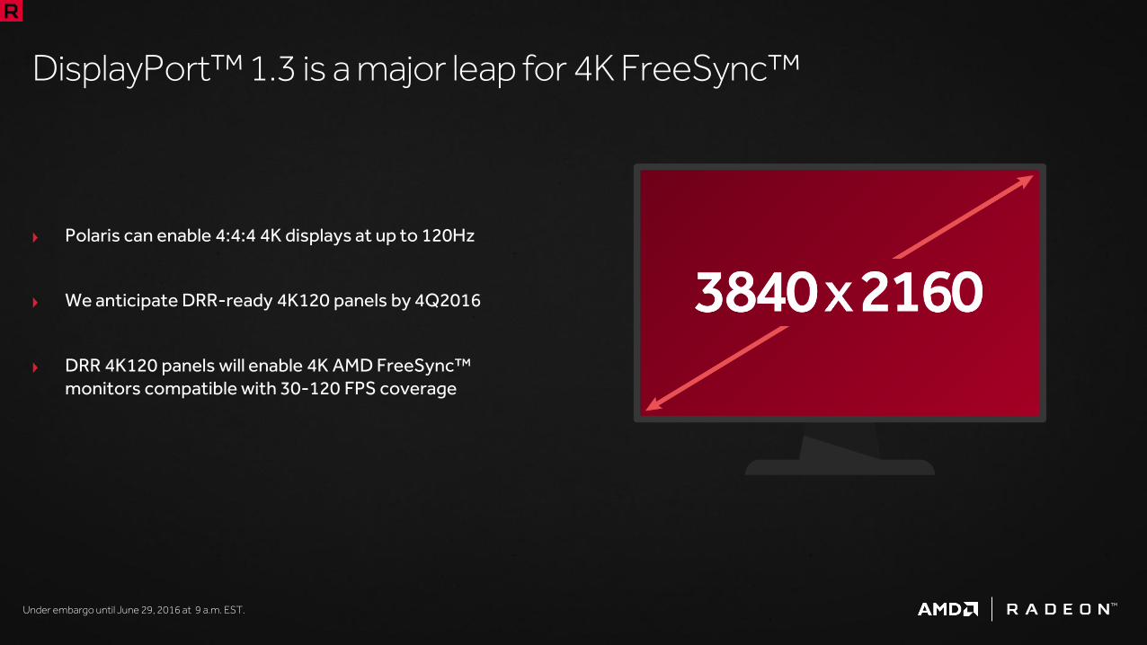
Polaris can enable 4:4:4 4K displays at up to 120Hz
We anticipate DRR-ready 4K120 panels by 4Q2016
DRR 4K120 panels will enable 4K AMD FreeSync™ monitors compatible with 30-120 FPS coverage
DisplayPort™ 1.3 is a major leap for 4K FreeSync™

Under embargo until June 29, 2016 at 9 a.m. EST.TM
Radeon™ RX 400 Series graphics will enable single-cable 4:4:4 5K60 resolution
5K is 78% more pixels than 3840x2160 (4K)
210ppi of 5K/28” provides incredible sharpnessand working space vs 142ppi of 4k/28”
We anticipate displays ready for single-cable 5K by year end
DisplayPort™ 1.3 enables single cable 5K60
Under embargo until June 29, 2016 at 9 a.m. EST.TM
X
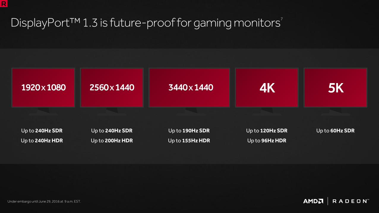
DisplayPort™ 1.3 is future-proof for gaming monitors7
Up to 240Hz SDR
Up to 200Hz HDR
Up to 240Hz SDR
Up to 240Hz HDR
Up to 190Hz SDR
Up to 155Hz HDR
Up to 120Hz SDR
Up to 96Hz HDR
Up to 60Hz SDR

Under embargo until June 29, 2016 at 9 a.m. EST.TM
The Polaris architecture is ready for home theater PCs
Under embargo until June 29, 2016 at 9 a.m. EST.
4K60
Under embargo until June 29, 2016 at 9 a.m. EST.TM
X
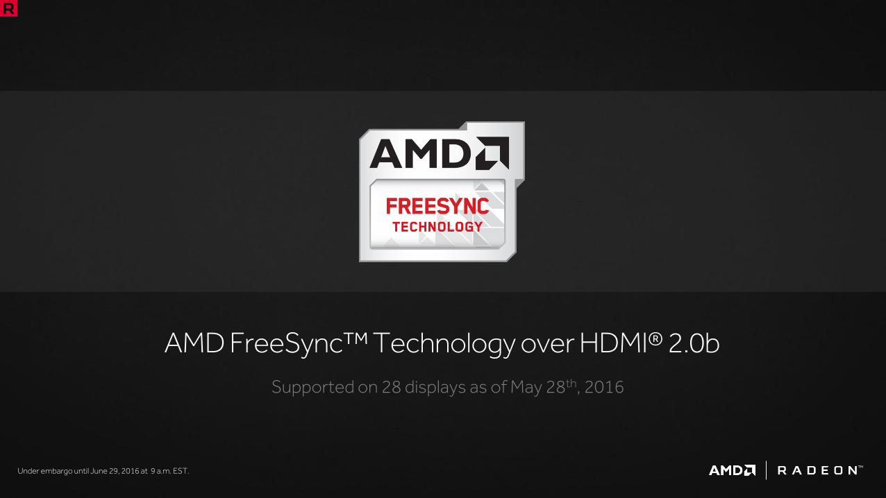
AMD FreeSync™ Technology over HDMI® 2.0b
Supported on 28 displays as of May 28th, 2016

Under embargo until June 29, 2016 at 9 a.m. EST.TM
AMD FreeSync™ Technology over HDMI® 2.0b
Technology Partners
Acer | LG | Mstar Semiconductor | Novatek | Realtek | Samsung

Under embargo until June 29, 2016 at 9 a.m. EST.TM
Polaris enables better pixels with HDR
Larger Color Spaces Higher Contrast Ratios Higher Peak Luminance

Under embargo until June 29, 2016 at 9 a.m. EST.TM
0
0.1
0.2
0.3
0.4
0.5
0.6
0.7
0.8
0.9
0 0.1 0.2 0.3 0.4 0.5 0.6 0.7 0.8 0.9
Human Visual Range sRGB Rec. 2020 Digital Cinema Typical WCG Monitor
HDR drives more colors
Typical monitors are sRGB (blue triangle)
Short-term HDR goal is to reach P3 DigitalCinema (yellow triangle)
Long-term HDR goal is to reach Rec. 2020(red triangle)
2X visible colors vs. sRGB
75% coverage of the human visual spectrum
Red/gold/cyan notably improved
Under embargo until June 29, 2016 at 9 a.m. EST.TM
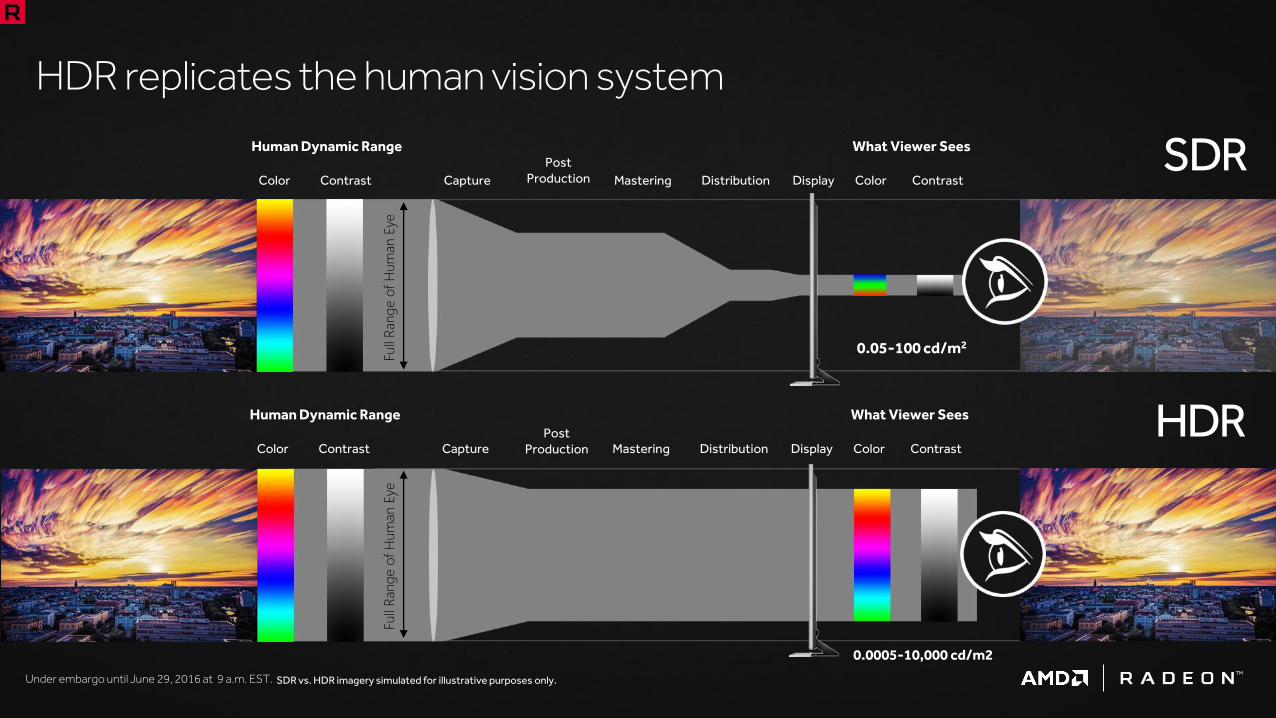
HDR replicates the human vision system
Full
Rang
e o
f H
um
an E
ye
Human Dynamic Range
Color Contrast Capture
PostProduction Mastering Distribution Display Color Contrast
What Viewer Sees SDR
0.05-100 cd/m2
Full
Rang
e o
f H
um
an E
ye
Human Dynamic Range
Color Contrast CapturePost
Production Mastering Distribution Display Color Contrast
What Viewer Sees HDR
0.0005-10,000 cd/m2
SDR vs. HDR imagery simulated for illustrative purposes only.

Under embargo until June 29, 2016 at 9 a.m. EST.TM
HDR drives higher luminance
Sunlight 1,600,000,000 nits
Fluorescent light 10,000 nits
Highlights 1,000-10,000 nits
White Range 250-1,000 nits
Typical Objects 1-250 nits
Shadow Details 0.01-1 nit
Ultra Blacks 0-0.01 nit
* Image courtesy “Russellstreet” under CC BY-SA 2.0 license from Flickr. Scene comparison simulated.
10,000 nits
~1 nit

Under embargo until June 29, 2016 at 9 a.m. EST.TM
HDR is better at translating bits to photons
Electro-Optical Transfer Functions are how we convert digital signals to light
Today’s consumer content is designed around CRT television EOTFs
Based on work started in 1930s
Only considers up to 100 nits of brightness
Wastes encoding bits and crushes black levels
10-bit ST 2084 is for HDR
Designed for the next 20 years of displays
Consistent encoding 0-10,000 nits
Dramatically improves detail/efficiency in black levels
0.1%
1.0%
10.0%
0.001 0.01 0.1 1 10 100 1000 10000
Min
imu
m C
on
tras
t S
tep
Brightness Nits
10-bit ST 2084 8-bit Gamma (100 Nit) 12-bit ST 2084 10-bit Gamma (1000 Nit) Human Vision

Under embargo until June 29, 2016 at 9 a.m. EST.TM
Polaris is ready for 10-bit and 12-bit HDR
First-gen HDR displays will be 10-bit
12-bit will exceed human visual acuity
Polaris architecture display pipe
Display color processing engine
Programmable gamut remapping
Programmable gamma control
Floating point processing
Enables 1:1 mapping with display’s native capabilities
Eliminates in-display remapping latency
Display ControllerFrame Buffer
32bpp Fixed Point
64bpp Floating Point
Floating Point Color Processing
Output Bit Depth Converter
8/10/12bpc color
8/10/12bpc colorDisplayPort™
HDMI®

Under embargo until June 29, 2016 at 9 a.m. EST.TM
Tonemapping should be done by the game engine
Tonemapping in the display adds significant input lag
We poll color/contrast/nits from the display
Polling fed back to engine tonemapper
Output from GPU optimized for the connected display
Switching to HDR tonemapping not a large hurdle
Game engines already do HDRR tonemapped to SDR
Available for developers now:
DirectX® 11 HDR driver support available for developers
DirectX® 12 support planned in a future driver update
HDR Video playback support available for developers
Radeon™ Photon SDK for HDR gaming
0
0.1
0.2
0.3
0.4
0.5
0.6
0.7
0.8
0.9
0 0.1 0.2 0.3 0.4 0.5 0.6 0.7 0.8 0.9Human Visual Range sRGB Rec. 2020

Under embargo until June 29, 2016 at 9 a.m. EST.TM
Polaris architecture HDR display support
HDMI® 2.0b(with HDCP 2.2)
1920x1080 @ 192Hz
2560x1440 @ 96Hz
3840x2160 @ 60Hz (4:2:2)
DisplayPort™ 1.4-HDR(with HDCP 2.2)
1920x1080 @ 240Hz
2560x1440 @ 192Hz
3840x2160 @ 96Hz

Under embargo until June 29, 2016 at 9 a.m. EST.TM
Accelerated Video Encoding & Decoding

Under embargo until June 29, 2016 at 9 a.m. EST.TM
A history of AMD’s video encode accelerator
Radeon™ HD 7970H.264 up to 1080p75
Radeon™ R9 290XH.264 up to 1080p75
Radeon™ R9 285H.264 up to 4K60
Radeon™ R9 Fury XH.264 up to 4K30

Under embargo until June 29, 2016 at 9 a.m. EST.TM
Video encode acceleration with Polaris
H.264 HEVC*
1080p120 1080p240
1440p60 1440p120
4K30 4K60
* HEVC acceleration is subject to inclusion/installation of HEVC-compatible applications.

Under embargo until June 29, 2016 at 9 a.m. EST.TM
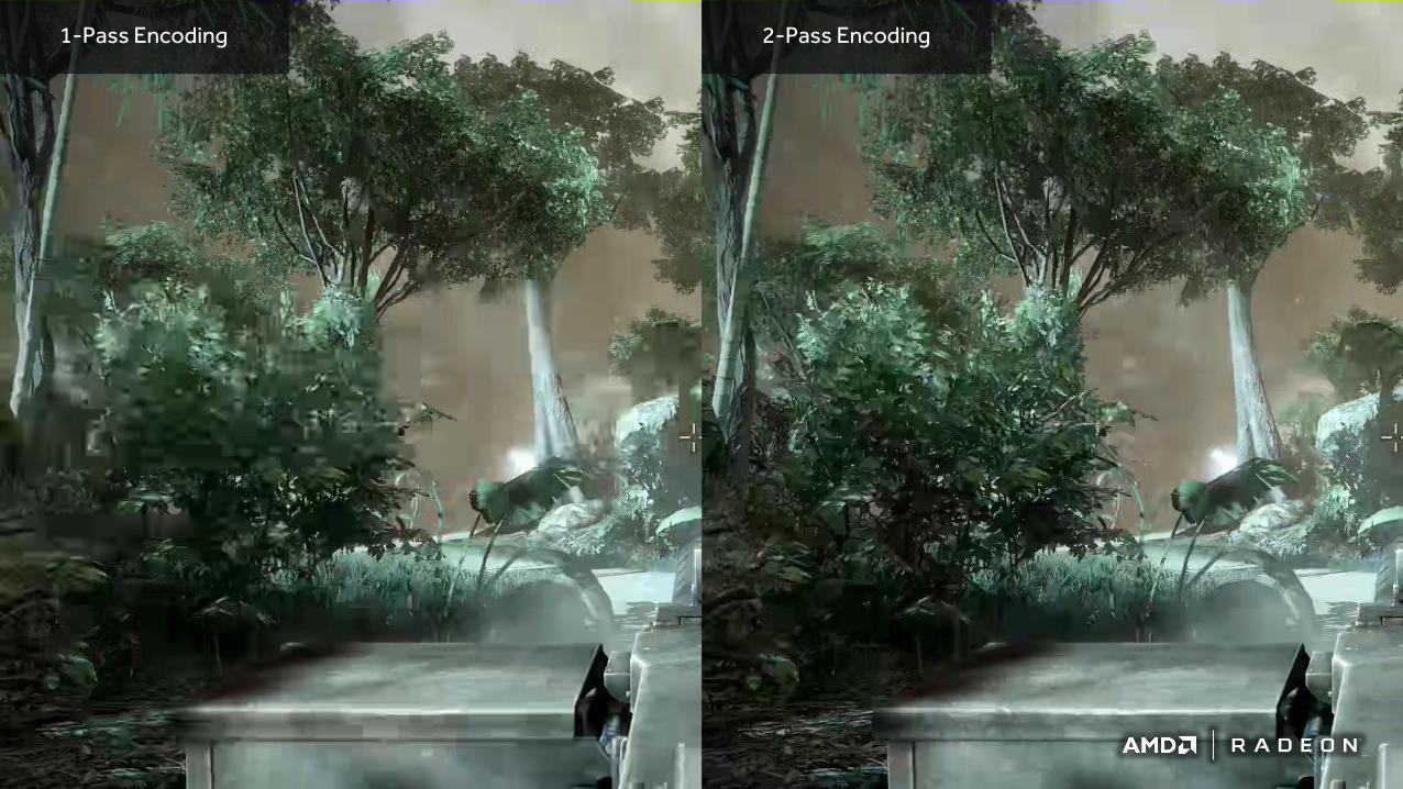
Improving stream quality with Polaris
Fast HQ encode is a tough problem
Rapid scene changes
Non-uniform complexity distribution
Achieving fast quality with 2-pass encoding
Downscaled pre-encode guides rate control
Picture-level analysis for efficient budget allocation
Macroblock-level analysis for efficient QP selection
2-pass encoding yields up to 1dB Y-PSNR gain
Works with H.264 and HEVC content
Warhammer, the Warhammer logo, GW, Games Workshop, The Game of Fantasy Battles, the twin-tailed
comet logo, and all associated logos, illustrations, images, names, creatures, races, vehicles, locations,
weapons, characters, and the distinctive likeness thereof, are either ® or TM, and/or © Games Workshop
Limited, variably registered around the world, and used under licence. Developed by Creative Assembly
and published by SEGA. Creative Assembly, the Creative Assembly logo, Total War and the Total War logo
are either registered trade marks or trade marks of The Creative Assembly Limited.
Under embargo until June 29, 2016 at 9 a.m. EST.TM
2-Pass Encoding1-Pass Encoding

Under embargo until June 29, 2016 at 9 a.m. EST.TM
Leveraging the Polaris architecture encode accelerator for games
* Use of third party logos is for informational purposes only and no endorsement of or by AMD is intended or implied.

Under embargo until June 29, 2016 at 9 a.m. EST.TM
A history of AMD’s video decode accelerator
Radeon™ HD 7970H.264 up to 1080p60VC1 up to 1080p60
MP4-P2 up to 1080p60
Radeon™ R9 290XH.264 up to 1080p60VC1 up to 1080p60
MP4-P2 up to 1080p60
Radeon™ R9 285H.264 up to 4K120VC1 up to 1080p60
MP4-P2 up to 1080p60
Radeon™ R9 Fury XH.264 up to 4K120
Main HEVC up to 4K60VC1 up to 1080p60
MP4-P2 up to 1080p60

Under embargo until June 29, 2016 at 9 a.m. EST.TM
Our most versatile decode accelerator yet
H.264Up to 4K120
HEVCUp to 4K60
Main-10
VP9Up to 4K
9MP4-P2
Up to 1080p60VC1
Up to 1080p60MJPEG
Up to 4K30

Under embargo until June 29, 2016 at 9 a.m. EST.TM
The Polaris architecture accelerates the best content
Beautiful HDR Movies(10-bit HEVC)
More Cat Videos(VP9)
Razor-Sharp Video Calling(HEVC & MJPEG)
Your Favorite Streamers(H.264)
* Logos for illustrative purposes only; no endorsement implied.

Under embargo until June 29, 2016 at 9 a.m. EST.TM
Optimizing FinFET 14

Under embargo until June 29, 2016 at 9 a.m. EST.TM
It’s been a long road
90nm2005
80nm2006
65nm2007
55nm2007
40nm2009
28nm2011
FinFET2016

Under embargo until June 29, 2016 at 9 a.m. EST.TM
Transistors per area have doubled effectively every 2 years
Sub-nm range, static leakage/area also doubling
Voltage reductions from technology flattened
Many PD techniques can reduce leakage; mitigate poor scaling
Power gating
Voltage islands
Back bias or advanced circuits
Unfortunately: a poor substitute for native process benefits
Drive to lower power consumption

Under embargo until June 29, 2016 at 9 a.m. EST.TM
FinFET 14 performance vs. 28nm planar
FinFET offers product level performance advantage over 28A planar
Significant variation reduction and leakage power improvement
FinFETs have fundamentally lower variation than planar bulk
Performance
28nm FinFETLo
g L
eak
age
* Diagram for illustrative purposes.

Under embargo until June 29, 2016 at 9 a.m. EST.TM
FinFET 14 has better variation
Leakage PowerP
erf
orm
ance
Performance
FinFET 14
28nm
Lower variation improves product performance and power
Performance set by the slowest device and the required voltage
Power set by the leakiest device
FinFETs have fundamentally lower variation than planar bulk
Lower power
* Diagram for illustrative purposes.

Under embargo until June 29, 2016 at 9 a.m. EST.TM
FinFET performance/power benefit
Relative Power
Re
lati
ve
Fm
ax
FinFET
28nm
Bottom line
FinFET devices provide fundamental performance / power benefit over planar
* Diagram for illustrative purposes.

Under embargo until June 29, 2016 at 9 a.m. EST.TM
FinFETs are a very significant step
Reduced operating voltages
Reduced leakage
Fundamental improvement in power efficiency
FinFETs enable new product categories
Thin & light gaming notebooks
Small form factor desktops
Discrete cards with fewer power connectors
Summarizing FinFET 14
Under embargo until June 29, 2016 at 9 a.m. EST.TM
Design Approaches for Power Efficiency

Under embargo until June 29, 2016 at 9 a.m. EST.TM
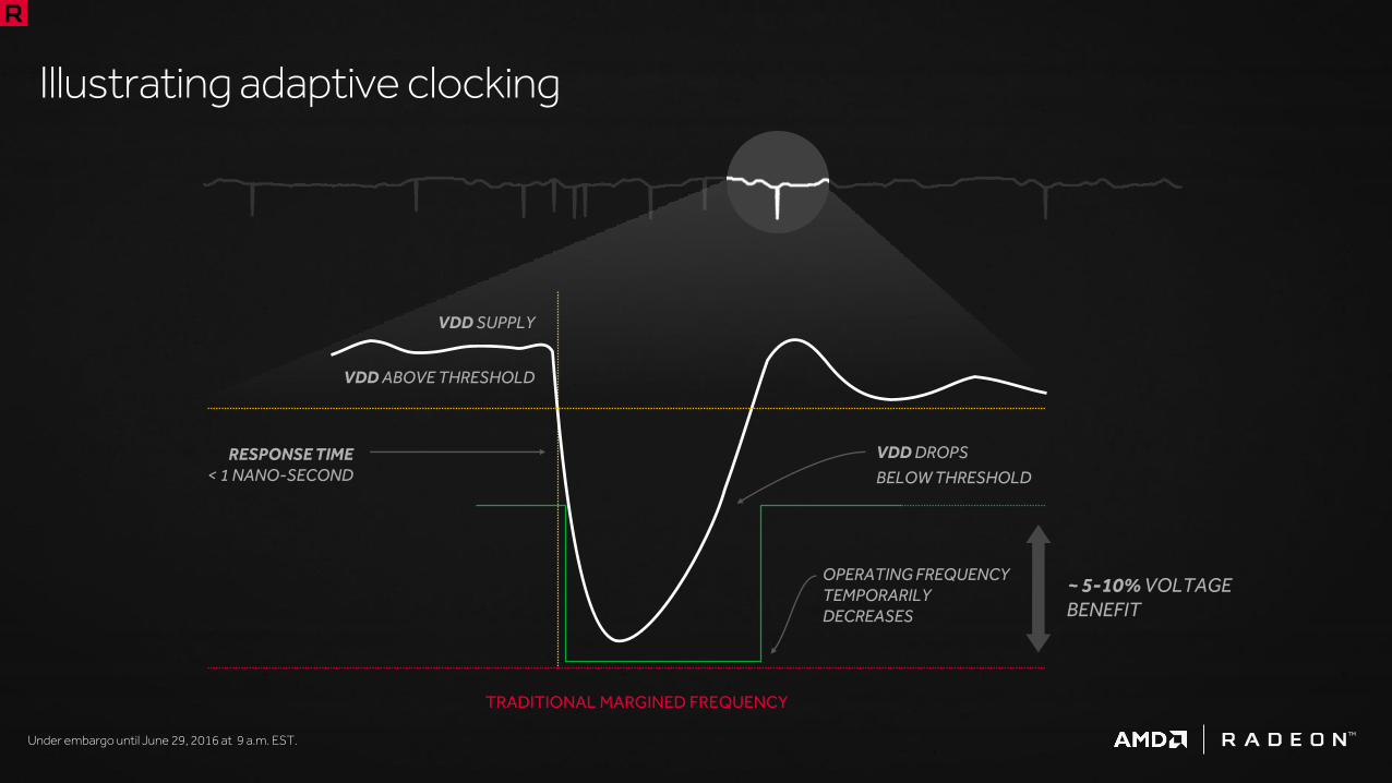
All GPUs operate at low voltages with high current
Challenging to deliver quality voltage from packages and power supplies
Voltage variations can be 10%-15% of the nominal value
Average voltage must be raised to cover this variation, which wastes a lot of power
AMD’s adaptive clocking recovers that waste with up to a 25% power reduction
Adaptive clocking
Measured Droop Improvements on Polaris 10
0.8V 0.9V 0.9V 1.0V 1.0V 1.1V 1.1V 1.2V 1.2V 1.3V
Me
asu
red
Vo
lta
ge
Dro
op
(Vse
t-V
de
v)
Vset
CKS OFF CKS ON
Under embargo until June 29, 2016 at 9 a.m. EST.TM
Illustrating adaptive clocking
VDD DROPS
BELOW THRESHOLD
RESPONSE TIME< 1 NANO-SECOND
TRADITIONAL MARGINED FREQUENCY
OPERATING FREQUENCYTEMPORARILY DECREASES
~ 5-10% VOLTAGE BENEFIT
VDD SUPPLY
VDD ABOVE THRESHOLD

Under embargo until June 29, 2016 at 9 a.m. EST.TM
Adaptive voltage & frequency scaling (AVFS)
Reliably extract the true silicon speed capability of the GPU
Including: part-to-part processing, temperature and power delivery
How: add a frequency sensor to existing power and temp sensors
Enables accurate setting of the optimal operating point
Optimal energy efficiency across the entire ASIC process, voltage, and temperature
Individual speed and voltage sensors distributed around the graphics core

Under embargo until June 29, 2016 at 9 a.m. EST.TM
Illustrating AVFS on the Polaris architecture
Voltage
Fre
qu
en
cy
Guard band required due to AC+DC voltage margins, temperature inversion and aging
True Si Fmax capability
Traditional DPM-states.
AVFS reduces the voltage required for the same
frequency
AVFS DPM-states.
* Diagram for illustrative purposes.

Under embargo until June 29, 2016 at 9 a.m. EST.TM
Run voltage analysis code on a tester when the part is tested and binned
Log the voltage as seen by the integrated power supply monitors
Run the same code on PC boot and observe voltage
Dial board vregs to deliver the same voltage as observed on the tester
Helps eliminate waste power usually spent accommodating board/system variation
Boot time power supply calibration (BTC)
PSMs observe the minimum voltage on the tester
VVAVG_TST
VAVG_SYS
Same PSMs observe the voltage on each boot in the system
Differences are compensated out
* Diagram for illustrative purposes.

Under embargo until June 29, 2016 at 9 a.m. EST.TM
GPUs require 2-3% clockspeed margin to accommodate transistor aging
Other aspects of the system also exhibit aging (e.g. lower voltage from system)
We want our parts to self-calibrate and adapt to changes over time – good or bad
More robust operation over time
Out-of-box performance is improved
Adaptive aging compensation
Exploit boot time calibration and aging-sensitive circuits in the AVFS modules
Vmin dialed in to compensate for
aging effects
VVAVG_SYS
* Diagram for illustrative purposes.

Under embargo until June 29, 2016 at 9 a.m. EST.TM
Specially-designed banks (MBFFs) that share circuitry
Critical clock sequence storage elements
There are approx. 21 million flip-flops in Polaris 10
They utilize about 15% of ASIC TDP
Save significant internal and sClk power
4-5% TDP savings
Multi-bit flip-flop (MBFF)
Up to 40% total clock power savings
with quad MBFF

Under embargo until June 29, 2016 at 9 a.m. EST.TM
Reducing memory bandwidth dependence:
Double L2 cache
Improve L2 utilization and efficiency
Improve LDCC algorithms and usage
Simultaneously reduce energy / bit
FinFETs help
Optimized interface design
Power gating, clock gating
Energy efficient memory interface
320GB/s
256GB/s
0%
20%
40%
60%
80%
100%
120%
140%
160%
R9 290 Polaris 10
Energy Efficient Memory
Bandwidth Performance / bit

Under embargo until June 29, 2016 at 9 a.m. EST.TM
Reducing memory bandwidth dependence:
Double L2 cache
Improve L2 utilization and efficiency
Improve LDCC algorithms and usage
Simultaneously reduce energy / bit
FinFETs help
Optimized interface design
Power gating, clock gating
Energy efficient memory interface
0%
20%
40%
60%
80%
100%
120%
140%
160%
R9 290 Polaris 10
Energy Efficient Memory
Energy / bit Performance / bit

Under embargo until June 29, 2016 at 9 a.m. EST.TM
320GB/s
256GB/s
0%
20%
40%
60%
80%
100%
120%
140%
160%
R9 290 Polaris 10
Energy Efficient Memory
Energy / bit Memory power Bandwidth Performance / bit
Lower Energy per bit
Better performance per bit
Outcome:
Memory bandwidth needs reduced
Total memory interface power reducedby up to 58%5
Energy efficient memory interface
58%Power
Savings

Under embargo until June 29, 2016 at 9 a.m. EST.TM
14nm FinFET optimized by AMD
1.7xPerformance / Watt
With FinFET 146
2.8xPerformance / Watt
With AMD technologies2
UP TOUP TO
Baseline
Technology
Arch + Features
0%
50%
100%
150%
200%
250%
300%
Performance / Watt Gains
Baseline(28nm Planar)
FinFET 14 Δ
FinFET 14 &
AMD IP

Under embargo until June 29, 2016 at 9 a.m. EST.TM
24.5 x 24.529x 29
“Bonaire” Polaris 11
L x W
“Bonaire” Polaris 11
1.9mm1.5mm
Z-Height
Radeon™ RX 460 graphics
TM
®
Under embargo until June 29, 2016 at 9 a.m. EST.TM
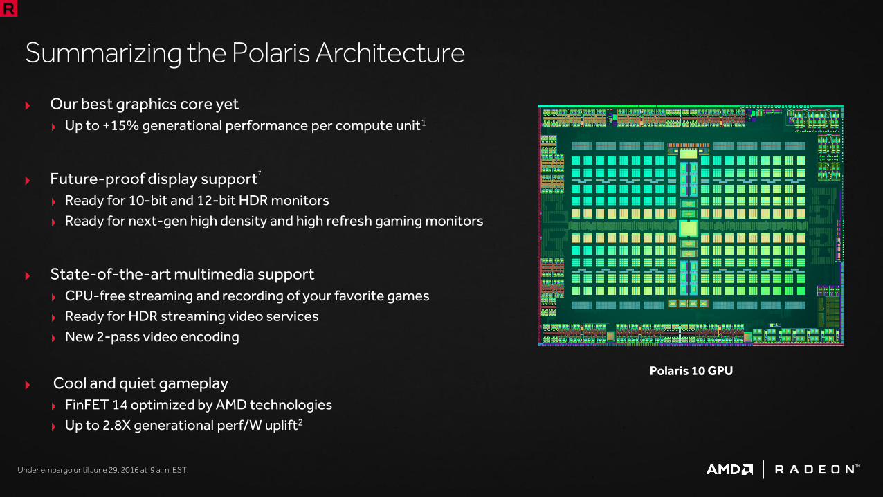
Our best graphics core yet
Up to +15% generational performance per compute unit1
Future-proof display support7
Ready for 10-bit and 12-bit HDR monitors
Ready for next-gen high density and high refresh gaming monitors
State-of-the-art multimedia support
CPU-free streaming and recording of your favorite games
Ready for HDR streaming video services
New 2-pass video encoding
Cool and quiet gameplay
FinFET 14 optimized by AMD technologies
Up to 2.8X generational perf/W uplift2
Summarizing the Polaris Architecture
Polaris 10 GPU

Under embargo until June 29, 2016 at 9 a.m. EST.TM
1. Testing conducted by AMD performance labs as of May 18, 2016 on the Radeon RX 480 and Radeon R9 290 on a test system comprising Intel Core i7-5960X, 16GB DDR4-2666, Gigabyte X99-UD4, Windows 10 x64 (build 10586), Radeon Software Crimson Edition 16.5.2using Ashes of Singularity, GTA V, Project Cars, Witcher, and Assassin’s Creed Syndicate, All games tested at 1440p. Radeon RX 480 graphics (150W TGP/36 CU) vs. Radeon R9 290 graphics (275W TGP/40 CU) scores as follows: Ashes of the Singularity (44.19 FPS vs 46 FPS); GTA V (66.23 FPS vs. 66.44 FPS); Project Cars (48.99 FPS vs. 45.99 FPS); Witcher 3 (50.78 FPS vs. 50.13 FPS); Assassin’s Creed Syndicate (50.51 FPS vs. 45.78 FPS). Average FPS of above game scores: 52.14 (Radeon RX 480) vs. 50.06 (Radeon R9 290). Discrete AMD Radeon™ GPUs and AMD FirePro™ GPUs based on the Graphics Core Next architecture consist of multiple discrete execution engines known as a Compute Unit (“CU”). Each CU contains 64 shaders (“Stream Processors”) working in unison (GD-78). CU efficiency formula = average FPS/# of CUs. Test results are not average and may vary. RX-4
2. Testing conducted by AMD Performance Labs as of May 10, 2016 on the AMD Radeon™ RX 470 (110w) and AMD Radeon™ R9 270X (180w), on a test system comprising i7 5960X @ 3.0 GHz 16GB memory, AMD Radeon Software driver 16.20 and Windows 10. Using 3DMark Fire Strike preset 1080p the scores were 9090 and 5787 respectively. Using Ashes of the Singularity 1080P High, the scores were 46 fps and 28.1 fps respectively. Using Hitman 1080p High, the scores were 60 fps and 27.6 fps respectively. Using Overwatch 1080p Max settings, the scores were 121 fps and 76 fps respectively. Using Performance/Board power, the resulting average across the 4 different titles was a perf per watt of 2.8X vs the Radeon R9 270X. Test results are not average and may vary. RX-6
3. Based on AMD internal small prim filter test. Primitive assembly rates with prim filter ON vs. OFF: 18 tri/px (3.947 vs. 1.255), 32 tri/px (3.901 vs. 1.773), 50 tri/px (3.760 vs. 1.402), 72 tri/px (3.303 vs. 1.187), 98 tri/px (3.928 vs. 1.171), 128 tri/px (3.870 vs. 1.111). System configuration: Radeon™ RX 480, Core i7-6700K, 16GB DDR4-2666, Windows 10 x64, Radeon™ Software 16.5.2.
4. Based on AMD internal memory bandwidth test. Radeon™ R9 290X: 263GB/s peak memory bandwidth. Radeon™ R9 Fury: 333 peak GB/s without DCC vs. 387 peak GB/s with DCC. Radeon™ RX 480: 186 peak GB/s without DCC vs. 251 peak GB/s with DCC. System configuration: Core i7-6700K, 16GB DDR4-2666, Windows 10 x64, Radeon™ Software 16.5.2.
5. Based on measurements of total memory interface power in watts conducted by the AMD performance labs as of 5/21/2016. System configuration: Radeon™ R9 290 vs. Radeon™ RX 480, Core i7-5960X, Gigabyte GA-X99-UD7, 16GB DDR4-2666, Windows 10 x64, Radeon™ Software 16.5.2.
6. Based on AMD internal data generated in AMD performance labs as of May 2016, measurements of capacitance, voltage frequency, leakage and power data show up to 1.7x performance/watt on 14nm vs 28nm FINFET technology. Final performance/watt results on AMD products using 14nm FinFET technology may vary and will depend on various factors including but not limited to clock speed, voltage, and various AMD proprietary technologies. RX-17
7. Statement of “future-proof” refers to support of current and upcoming technology standards including 14nm FinFET process technology, DirectX®12 and Vulkan™ API support, new display technology, and experiences such as VR. “Future-proof” statement is not meant to serve as a warranty or indicate that users will never have to upgrade their graphics technology again. Support of current and upcoming technology standards described above has the potential to reduce frequency of graphics upgrades for some users.
8. One compute unit on an AMD Radeon™ GPU is equal to 64 stream processors.
9. Hardware-accelerated VP9 decode support is planned for enablement in a future Radeon™ Software driver release.
Footnotes

Under embargo until June 29, 2016 at 9 a.m. EST.TM
Disclaimer & Attribution
The information presented in this document is for informational purposes only and may contain technical inaccuracies, omissions and typographical errors.
The information contained herein is subject to change and may be rendered inaccurate for many reasons, including but not limited to product and roadmap changes, component and motherboard version changes, new model and/or product releases, product differences between differing manufacturers, software changes, BIOS flashes, firmware upgrades, or the like. AMD assumes no obligation to update or otherwise correct or revise this information. However, AMD reserves the right to revise this information and to make changes from time to time to the content hereof without obligation of AMD to notify any person of such revisions or changes.
AMD MAKES NO REPRESENTATIONS OR WARRANTIES WITH RESPECT TO THE CONTENTS HEREOF AND ASSUMES NO RESPONSIBILITY FOR ANY INACCURACIES, ERRORS OR OMISSIONS THAT MAY APPEAR IN THIS INFORMATION.
AMD SPECIFICALLY DISCLAIMS ANY IMPLIED WARRANTIES OF MERCHANTABILITY OR FITNESS FOR ANY PARTICULAR PURPOSE. IN NO EVENT WILL AMD BE LIABLE TO ANY PERSON FOR ANY DIRECT, INDIRECT, SPECIAL OR OTHER CONSEQUENTIAL DAMAGES ARISING FROM THE USE OF ANY INFORMATION CONTAINED HEREIN, EVEN IF AMD IS EXPRESSLY ADVISED OF THE POSSIBILITY OF SUCH DAMAGES.
ATTRIBUTION
©2016 Advanced Micro Devices, Inc. All rights reserved. AMD, the AMD Arrow logo, [insert all other AMD trademarks used in the material here per AMD’s Checklist for Trademark Attribution] and combinations thereof are trademarks of Advanced Micro Devices, Inc. Other product names used in this publication are for identification purposes only and may be trademarks of their respective companies.
The terms HDMI and HDMI High-Definition Multimedia Interface, and the HDMI Logo are trademarks or registered trademarks of HDMI Licensing LLC in the United States and other countries.