tm the act3780 is a complete battery-charging and sheets/active-semi pdf's/act37… ·...
TRANSCRIPT
Innovative PowerTM - 1 - www.active-semi.com Copyright © 2013 Active-Semi, Inc. Active-Semi Proprietary For Authorized Recipients and Customers
ActivePathTM is a trademark of Active-Semi.
ACT3780Rev 8, 09-Jul-13
ActivePathTM Battery Charger
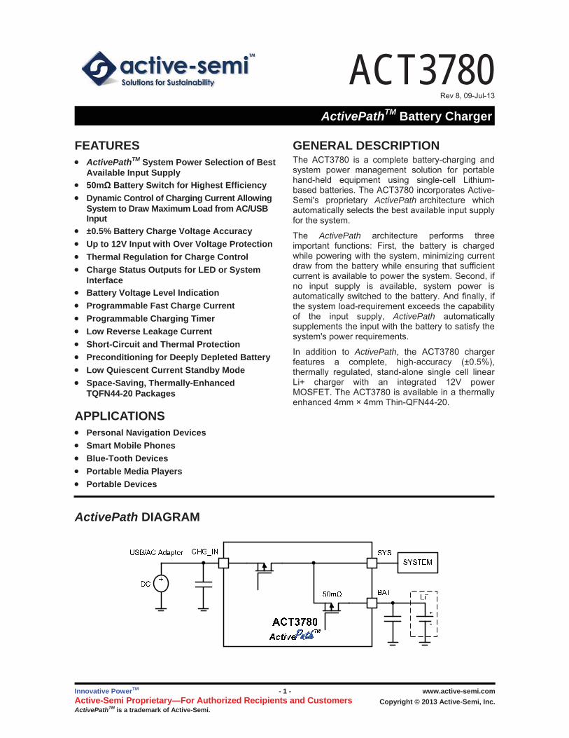
ActivePath DIAGRAM
FEATURES ActivePathTM System Power Selection of Best Available Input Supply 50m Battery Switch for Highest Efficiency Dynamic Control of Charging Current Allowing System to Draw Maximum Load from AC/USB Input ±0.5% Battery Charge Voltage Accuracy Up to 12V Input with Over Voltage Protection Thermal Regulation for Charge Control Charge Status Outputs for LED or System Interface Battery Voltage Level Indication Programmable Fast Charge Current Programmable Charging Timer Low Reverse Leakage Current Short-Circuit and Thermal Protection Preconditioning for Deeply Depleted Battery Low Quiescent Current Standby Mode Space-Saving, Thermally-Enhanced TQFN44-20 Packages
APPLICATIONS Personal Navigation Devices Smart Mobile Phones Blue-Tooth Devices Portable Media Players Portable Devices
GENERAL DESCRIPTION The ACT3780 is a complete battery-charging and system power management solution for portable hand-held equipment using single-cell Lithium-based batteries. The ACT3780 incorporates Active-Semi's proprietary ActivePath architecture which automatically selects the best available input supply for the system.
The ActivePath architecture performs three important functions: First, the battery is charged while powering with the system, minimizing current draw from the battery while ensuring that sufficient current is available to power the system. Second, if no input supply is available, system power is automatically switched to the battery. And finally, if the system load-requirement exceeds the capability of the input supply, ActivePath automatically supplements the input with the battery to satisfy the system's power requirements.
In addition to ActivePath, the ACT3780 charger features a complete, high-accuracy (±0.5%), thermally regulated, stand-alone single cell linear Li+ charger with an integrated 12V power MOSFET. The ACT3780 is available in a thermally enhanced 4mm × 4mm Thin-QFN44-20.
ACT3780Rev 8, 09-Jul-13
Innovative PowerTM - 2 - www.active-semi.com Copyright © 2013 Active-Semi, Inc. Active-Semi Proprietary For Authorized Recipients and Customers
ActivePathTM is a trademark of Active-Semi.
ORDERING INFORMATION
PART NUMBER BATTERY VOLTAGE
SYSTEM VOLTAGE PACKAGE PINS TEMPERATURE
RANGE
ACT3780QY-T 4.2V 4.6V TQFN44-20 20 -40°C to 85°C
ACT3780QY410-T 4.1V 4.6V TQFN44-20 20 -40°C to 85°C
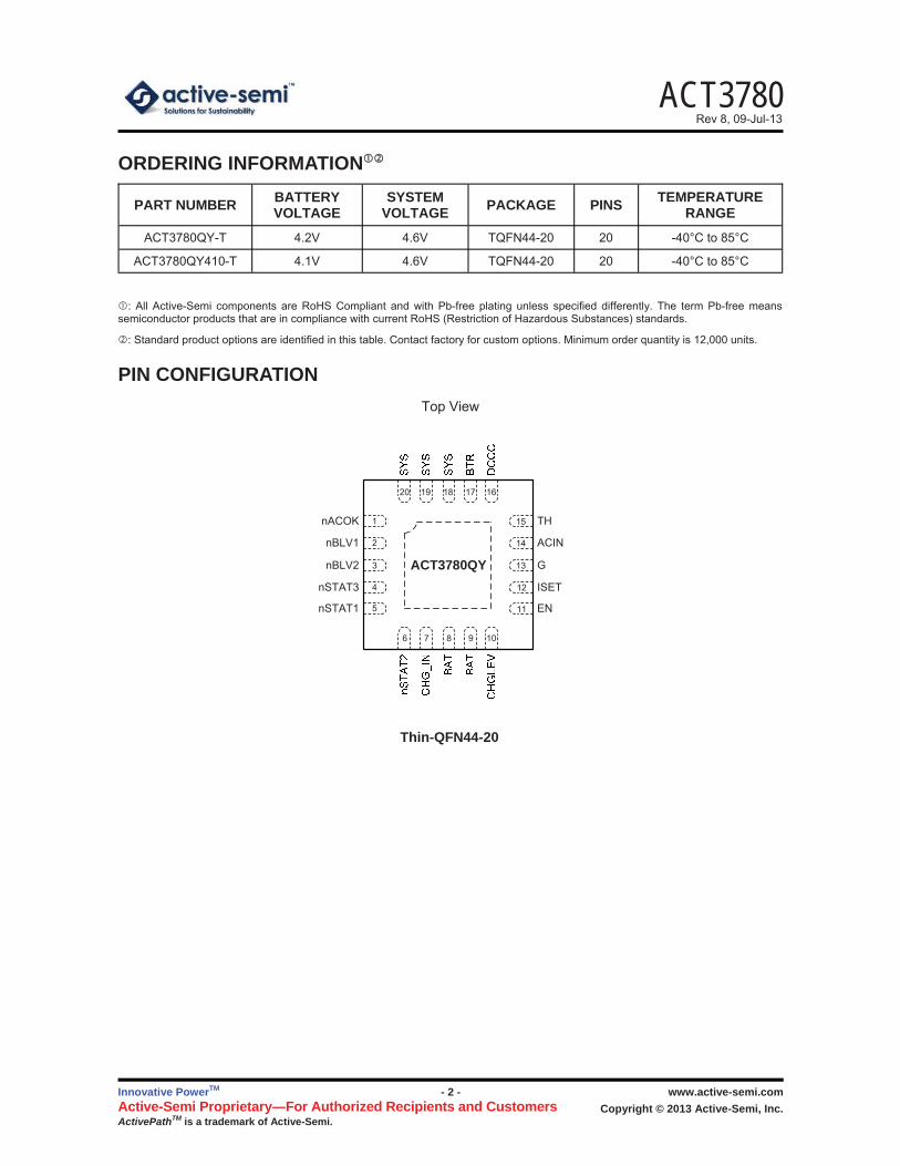
PIN CONFIGURATION
: All Active-Semi components are RoHS Compliant and with Pb-free plating unless specified differently. The term Pb-free means semiconductor products that are in compliance with current RoHS (Restriction of Hazardous Substances) standards.
: Standard product options are identified in this table. Contact factory for custom options. Minimum order quantity is 12,000 units.
Thin-QFN44-20
Top View
1nACOK
2
3
4
5
6 7 8 9 10
15
14
13
12
11
20 19 18 17 16
nBLV1
nBLV2
nSTAT3
nSTAT1
TH
ACIN
G
ISET
EN
ACT3780QY
ACT3780Rev 8, 09-Jul-13
Innovative PowerTM - 3 - www.active-semi.com Copyright © 2013 Active-Semi, Inc. Active-Semi Proprietary For Authorized Recipients and Customers
ActivePathTM is a trademark of Active-Semi.
PIN DESCRIPTIONS PIN NAME DESCRIPTION
1 nACOK CHG_IN Status Output. nACOK is an open-drain which sinks current whenever VCHG_IN is within it's valid operating range.
2 nBLV1 Battery Voltage level Monitor Output 1. Open-drain output that sinks current when asserted. Connect a 10k or greater pull-up resistors between nBLV1 and a suitable voltage supply. See Battery Voltage Level Indication Section for more information.
3 nBLV2 Battery Voltage level Monitor Output 2. Open-drain output that sinks current when asserted. Connect a 10k or greater pull-up resistors between nBLV2 and a suitable voltage supply. See Battery Voltage Level Indication Section for more information.
4 nSTAT3 CHG_IN OVP Status Output. Open-drain output that sinks current whenever VCHG_IN is greater than OVP threshold 6.9V (typ) while battery is present. For a logic-level charge status indicator, simply connect a 10k or greater pull-up resistor between nSTAT3 and a suitable voltage supply.
5 nSTAT1
Charge State Indicator. Open-drain output with an internal 6mA current limit, allowing this pin to directly drive an indicator LED. For a logic-level charge status indicator, simply connect a 10k or greater pull-up resistor between nSTAT1 and a suitable voltage supply. See the Charging Status Indication Section for more information.
13 G Ground.
7 CHG_IN Power Input. Bypass to G with a high quality ceramic capacitor placed as close to the IC as possible.
8, 9 BAT Battery Charger output. Connect this pin to the positive terminal of the battery. Bypass to G with a high quality ceramic capacitor placed as close to the IC as possible.
10 CHGLEV Charging State Select Input. Drive CHGLEV to VSYS or to a logic high for high-current charging mode or drive to G or a logic low for low-current charging mode. See the ACIN and CHGLEV Inputs section for more information.
11 EN EN Charger Enable Input. Drive to a logic high to enable IC, drive to a logic low to disable the device and enter suspend mode.
12 ISET Charge Current Set Input. Connect a resistor from ISET to G to set the fast-charge current.
14 ACIN AC Adaptor Detect Logic Input. Detects presence of a wall adaptor and automatically adjusts the charge current to the maximum charge current level. See the ACIN and CHGLEV Inputs section for more information.
15 TH Temperature Sensing Input. Connect to battery thermistor terminal. See the BatteryTemperature Monitoring section for more information.
16 DCCC Dynamic Control of Charging Current Set Input. Connect a resistor from DCCC to G to set the DCCC voltage. See the Dynamic Charge Current Control section for more information.
17 BTR Safety Timer Programming Input. Connect a resistor from BTR to G to set the safety timers. Do not leave this pin floating. See the Charging Safety Timers Section for more information.
18, 19, 20 SYS System Power Output. Bypass to G with a high quality ceramic capacitor placed as close to the
IC as possible.
EP Exposed Pad. Must be soldered to ground on the PCB.
6 nSTAT2
Charge State Indicator. Open-drain output with an internal 6mA current limit, allowing this pin to directly drive an indicator LED. For a logic-level charge status indicator, simply connect a 10k or greater pull-up resistor between nSTAT2 and a suitable voltage supply. See the Charging Status Indication Section for more information.
ACT3780Rev 8, 09-Jul-13
Innovative PowerTM - 4 - www.active-semi.com Copyright © 2013 Active-Semi, Inc. Active-Semi Proprietary For Authorized Recipients and Customers
ActivePathTM is a trademark of Active-Semi.
ABSOLUTE MAXIMUM RATINGS
ELECTRICAL CHARACTERISTICS
: Do not exceed these limits to prevent damage to the device. Exposure to absolute maximum rating conditions for long periods may affect device reliability.
(VCHG_IN = 5.0V, RISET = 1k , RBTR = 62k , RDCCC = 18.7k , TA = 25°C, unless otherwise specified.)
PARAMETER VALUE UNIT CHG_IN to G -0.3 to + 14 V
BAT, SYS, BTR, ISET, DCCC, ACIN, CHGLEV, EN, TH, nACOK, nSTAT1, nSTAT2, nSTAT3, nBLV1, nBLV2 to G -0.3 to + 6 V
Input Current 3.5 A
Output Current (Internal Limit) BAT to SYS 4 A
Maximum Junction Temperature -40 to 150 °C
Storage Temperature -60 to 150 °C
Lead Temperature (Soldering, 10 sec) 300 °C
PARAMETER SYMBOL TEST CONDITIONS MIN TYP MAX UNIT ActivePath
CHG_IN Voltage Range VCHG_IN 4.35 12 V
CHG_IN UVLO Voltage VUVLO Voltage Rising 3.65 3.85 4.05 V
CHG_IN UVLO Hysteresis VHYS(UVLO) 1.25 V
CHG_IN OVP Threshold VOVP Voltage Rising 6.60 6.90 7.20 V
CHG_IN OVP Hysteresis VHYS(OVP) 360 mV
CHG_IN Supply Current ISUP(CHG_IN)
VCHG_IN = 6V, VBAT float 60 200 μA
VCHG_IN = 6V, VBAT = 4.3V, ActivePathTM Enabled and SYS No Load, Charger in EOC or Time Out state or Disabled.
1.8 mA
CHG_IN to SYS On-Resistance RDSON_Q1 ISYS = 100mA 0.3 0.5
CHG_IN to SYS Current Limit
IAC ACIN = 1 2.5 A
IUSB ACIN = G, CHGLEV = G 80 90 100 mA
ACIN = G, CHGLEV = SYS 400 450 500 mA
SYS and DCCC Regulation
SYS Regulated Voltage VSYS_REG ISYS = 100mA 4.4 4.6 4.8 V
DCCC Pull-Up Current IDCCC 90 100 110 μA
ACT3780Rev 8, 09-Jul-13
Innovative PowerTM - 5 - www.active-semi.com Copyright © 2013 Active-Semi, Inc. Active-Semi Proprietary For Authorized Recipients and Customers
ActivePathTM is a trademark of Active-Semi.
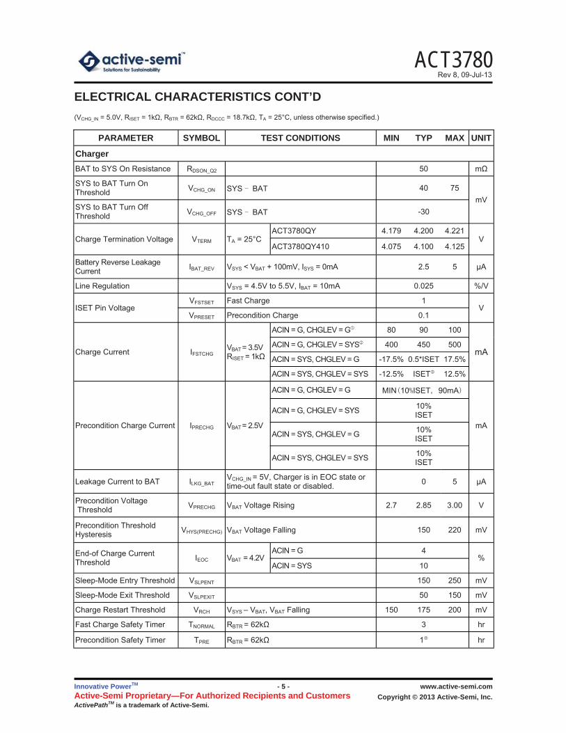
ELECTRICAL CHARACTERISTICS CONT’D (VCHG_IN = 5.0V, RISET = 1k , RBTR = 62k , RDCCC = 18.7k , TA = 25°C, unless otherwise specified.)
PARAMETER SYMBOL TEST CONDITIONS MIN TYP MAX UNIT
Charger BAT to SYS On Resistance RDSON_Q2 50 m
SYS to BAT Turn On Threshold VCHG_ON SYS BAT 40 75
mV SYS to BAT Turn Off Threshold VCHG_OFF SYS BAT -30
Charge Termination Voltage VTERM ACT3780QY 4.179 4.200 4.221
V ACT3780QY410 4.075 4.100 4.125
Battery Reverse Leakage Current IBAT_REV VSYS < VBAT + 100mV, ISYS = 0mA 2.5 5 μA
Line Regulation VSYS = 4.5V to 5.5V, IBAT = 10mA 0.025 %/V
ISET Pin Voltage VFSTSET Fast Charge 1
V VPRESET Precondition Charge 0.1
Charge Current IFSTCHG VBAT = 3.5V RISET = 1k
ACIN = G, CHGLEV = G 80 90 100
mA ACIN = G, CHGLEV = SYS 400 450 500
ACIN = SYS, CHGLEV = G -17.5% 0.5*ISET 17.5%
ACIN = SYS, CHGLEV = SYS -12.5% ISET 12.5%
Precondition Charge Current IPRECHG VBAT = 2.5V
ACIN = G, CHGLEV = G MIN 10 ISET 90mA
mA
ACIN = G, CHGLEV = SYS 10%ISET
ACIN = SYS, CHGLEV = G 10%ISET
ACIN = SYS, CHGLEV = SYS 10%ISET
Precondition Voltage Threshold VPRECHG VBAT Voltage Rising 2.7 2.85 3.00 V
Precondition Threshold Hysteresis VHYS(PRECHG) VBAT Voltage Falling 150 220 mV
End-of Charge Current Threshold IEOC VBAT = 4.2V
ACIN = G 4 %
ACIN = SYS 10
Sleep-Mode Entry Threshold VSLPENT 150 250 mV
Sleep-Mode Exit Threshold VSLPEXIT 50 150 mV
Charge Restart Threshold VRCH VSYS – VBAT, VBAT Falling 150 175 200 mV
Fast Charge Safety Timer TNORMAL RBTR = 62k 3 hr
Precondition Safety Timer TPRE RBTR = 62k 1 hr
TA = 25°C
Leakage Current to BAT ILKG_BAT VCHG_IN = 5V, Charger is in EOC state or time-out fault state or disabled. 0 5 μA
ACT3780Rev 8, 09-Jul-13
Innovative PowerTM - 6 - www.active-semi.com Copyright © 2013 Active-Semi, Inc. Active-Semi Proprietary For Authorized Recipients and Customers
ActivePathTM is a trademark of Active-Semi.
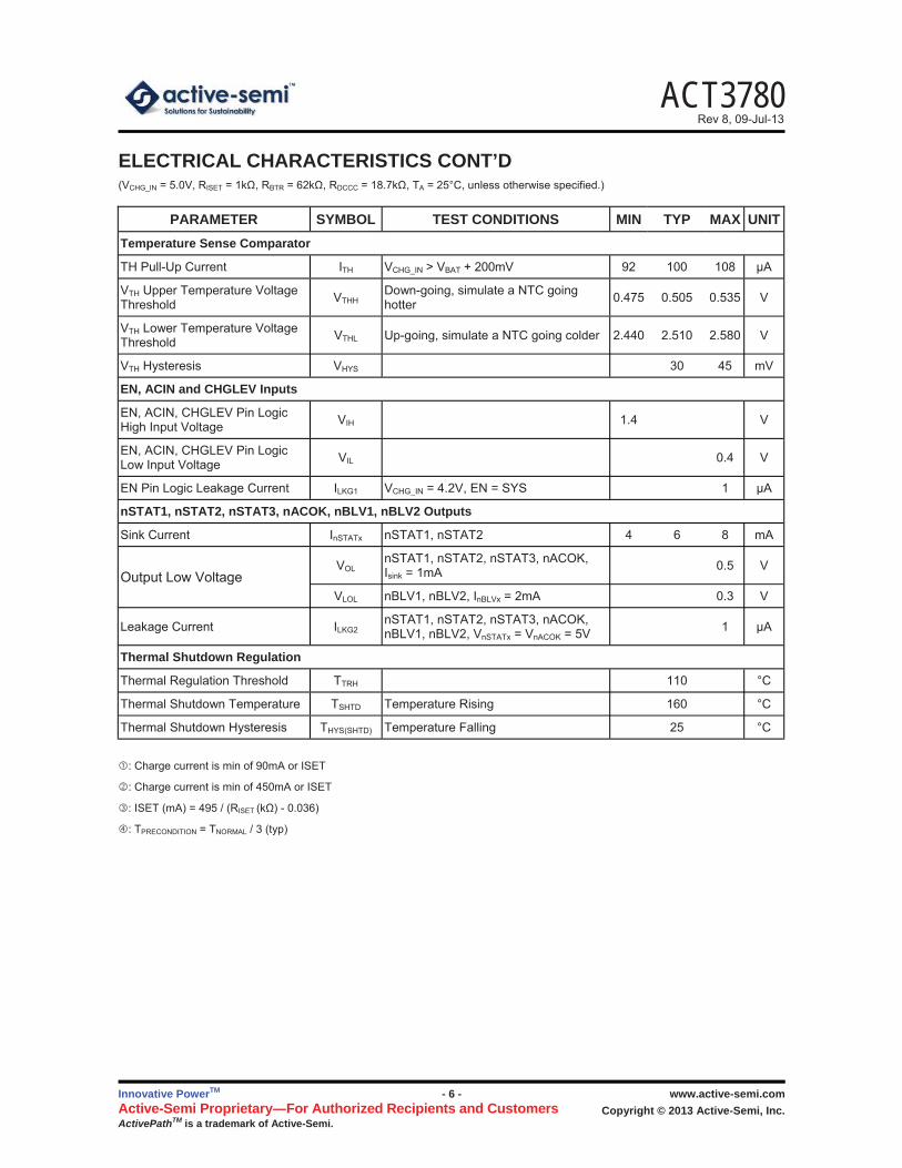
ELECTRICAL CHARACTERISTICS CONT’D (VCHG_IN = 5.0V, RISET = 1k , RBTR = 62k , RDCCC = 18.7k , TA = 25°C, unless otherwise specified.)
PARAMETER SYMBOL TEST CONDITIONS MIN TYP MAX UNIT Temperature Sense Comparator
TH Pull-Up Current ITH VCHG_IN > VBAT + 200mV 92 100 108 μA
VTH Upper Temperature Voltage Threshold VTHH Down-going, simulate a NTC going
hotter 0.475 0.505 0.535 V
VTH Lower Temperature Voltage Threshold VTHL Up-going, simulate a NTC going colder 2.440 2.510 2.580 V
VTH Hysteresis VHYS 30 45 mV
EN, ACIN and CHGLEV Inputs
EN, ACIN, CHGLEV Pin Logic High Input Voltage VIH 1.4 V
EN, ACIN, CHGLEV Pin Logic Low Input Voltage VIL 0.4 V
EN Pin Logic Leakage Current ILKG1 VCHG_IN = 4.2V, EN = SYS 1 μA
nSTAT1, nSTAT2, nSTAT3, nACOK, nBLV1, nBLV2 Outputs
Sink Current InSTATx nSTAT1, nSTAT2 4 6 8 mA
VOL nSTAT1, nSTAT2, nSTAT3, nACOK, Isink = 1mA 0.5 V
VLOL nBLV1, nBLV2, InBLVx = 2mA 0.3 V
Leakage Current ILKG2 nSTAT1, nSTAT2, nSTAT3, nACOK, nBLV1, nBLV2, VnSTATx = VnACOK = 5V 1 μA
Thermal Shutdown Regulation
Thermal Regulation Threshold TTRH 110 °C
Thermal Shutdown Temperature TSHTD Temperature Rising 160 °C
Thermal Shutdown Hysteresis THYS(SHTD) Temperature Falling 25 °C
Output Low Voltage
: Charge current is min of 90mA or ISET
: Charge current is min of 450mA or ISET
: ISET (mA) = 495 / (RISET (k ) - 0.036)
: TPRECONDITION = TNORMAL / 3 (typ)
ACT3780Rev 8, 09-Jul-13
Innovative PowerTM - 7 - www.active-semi.com Copyright © 2013 Active-Semi, Inc. Active-Semi Proprietary For Authorized Recipients and Customers
ActivePathTM is a trademark of Active-Semi.
ACIN
REF
VOLTAGE SENSE
110°C
THERMAL REGULATION G
System andCharger Control
ACT3780Body
Control
CURRENT SENSE
BodyControl
BAT
SYS CHG_IN
EN
CHGLEV
BTR
nBLV1
nBLV2
nACOK
nSTAT2
nSTAT1
TH
ISET
DCCC
+-
System SupplyAC Adaptor
USB
(Optional)
PRECONDITION
+–
+–
ThermalShutdown
VTHL
VTHH
EP
nSTAT3
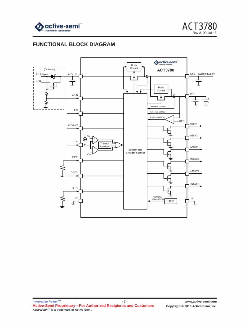
FUNCTIONAL BLOCK DIAGRAM
ACT3780Rev 8, 09-Jul-13
Innovative PowerTM - 8 - www.active-semi.com Copyright © 2013 Active-Semi, Inc. Active-Semi Proprietary For Authorized Recipients and Customers
ActivePathTM is a trademark of Active-Semi.
(1)
FUNCTIONAL DESCRIPTION The ACT3780 is a complete battery-charging and system power management solution for portable hand-held equipment using single-cell Lithium-based batteries. The ACT3780 incorporates Active-Semi's patent-pending ActivePath architecture which automatically selects the best available input supply for the system, and additionally features a complete, high-accuracy (±0.5%), thermally regulated, Full-Featured single cell linear Li+ charger with an integrated 12V power MOSFET.
ActivePath Architecture Active-semi's proprietary ActivePath architecture performs three important functions:
System Configuration OptimizationDepending upon the state of the input supply, ActivePath automatically optimizes the power system configuration. If the input supply is present, ActivePath powers the system in parallel with the battery, so that both system power and charge current can be independently managed to ensure that system power requirements are satisfied, the battery can charge as quickly as possible, and to ensure that the total system current does not exceed the capability of the input supply. If the input supply is not present, then ActivePath automatically configures the system to draw power from the battery. Finally, if the system current requirement exceeds the capability of the input supply, ActivePath automatically configures the battery to support the load in parallel with the input supply, to ensure maximum supply capability to the load under peak-power consumption conditions.
Input MOSFET Power (Q1) At the input of the ACT3780's ActivePath circuit is Q1, an integrated 12V power MOSFET. Q1 is part of an internal low-dropout linear regulator that regulates the system voltage (VSYS) to 4.6V, protecting the system from high-voltage input supplies. Q1 includes several features that can be used to limit the total current drawn from the input supply.
ACIN's current limit is determined primarily by the ACIN input, Q1 operates in “AC-Mode” when ACIN is driven to a logic-high, and Q1 operates in “USB-Mode” when driven to a logic-low. When operating in “AC-Mode”, Q1's internal current limit is programmed to 2.5A. When operating in “USB-Mode”, Q1's current limit is set to either 450mA,
when CHGLEV is driven to a logic-high, or to 90mA, when CHGLEV is driven to a logic-low. This functionality provides simple means of implementing a solution that operates within the current-capability limitations of the USB port while taking advantage of the high output current capability of AC adapters. For more information about the ACIN input, see the ACIN and CHGLEV Inputs section.
Dual-Function MOSFET (Q2) Q2 is a dual-function power MOSFET, that serves both as a low-resistance (50m ) switch that supplies the load current requirements of the system from the battery when no input supply is present or the system demands more current than the input can provide.
Current-Limits and Charge-Current Programming ACT3780 provides a flexible current programming scheme that combines the convenience of internal charge current programming with the flexibility of resistor-based charge current programming. Current limits and charge current programming are managed as a function of the ACIN and CHGLEV pins, in combination with RISET, the resistance connected to the ISET pin.
ACIN and CHGLEV Inputs ACIN is a logic input that configures the current-limit of input transistor (Q1) as well as that of the battery charger. ACIN features an logic input threshold, so that the input voltage detection threshold may be adjusted with a simple resistive voltage divider. This input also allows a simple, low-cost dual-input charger switch to be implemented with just a few, low-cost components. As shown in the Functional Block Diagram.
When ACIN is driven to a logic high, the ActivePath operates in “AC-Mode” and the charger charges at the current programmed by RISET,
When ACIN is driven to a logic-low, the ActivePath circuitry operates in “USB-Mode”, which enforces a maximum charge current setting of 450mA, if CHGLEV is driven to a logic-high, or 90mA, if CHGLEV is driven to a logic-low.
ISET(mA) = 495 / (RISET(k ) - 0.036)
ACT3780Rev 8, 09-Jul-13
Innovative PowerTM - 9 - www.active-semi.com Copyright © 2013 Active-Semi, Inc. Active-Semi Proprietary For Authorized Recipients and Customers
ActivePathTM is a trademark of Active-Semi.
ACIN CHGLEV Fast Charge Current High High ISET (mA) = 495 / (RISET (k ) - 0.036)
High Low 0.5 × ISET
Low High Min (450mA, ISET )
Low Low Min (90mA, ISET )
The ACT3780's charge current settings are summarized in the table below:
Table 1: ACIN and CHGLEV Inputs Table
Note that the actual charging current may be limited to a current that is lower than the programmed fast-charge current due to the ACT3780’s internal thermal regulation loop. See the Thermal Regulation and Protection section for more information.
Dynamic Charge Current Control (DCCC) The ACT3780's ActivePath Charger features Dynamic Charge Current Control (DCCC) circuitry, which continuously monitors the input supply to prevent input overload conditions. DCCC reduces the charge current when the SYS voltage decreases to VDCCC and stops charging when SYS drops below VDCCC by 1.5% (typical).
The DCCC voltage threshold is programmed by connecting a resistor from DCCC to GA according to the following equation:
Where RDCCC is the value of the external resistor, and IDCCC (100μA typical) is the value of the current sourced from DCCC.
Given the tolerances of the RDCCC and IDCCC ,the DCCC voltage threshold should be programmed to be no less than 3.3V to prevent triggering the UVLO, and to be no larger than 4.4V to prevent engaging DCCC prematurely. A 19.1k (1%), or 18.7k (1%) resistor for RDCCC is recommended.
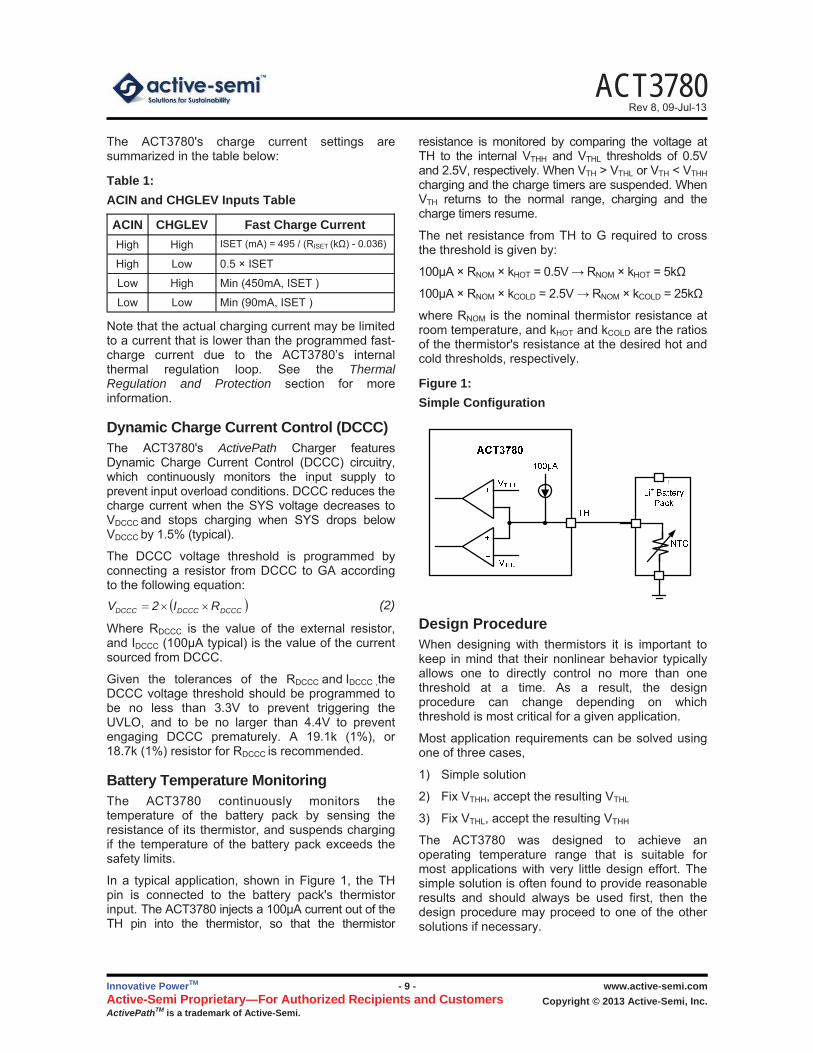
Battery Temperature Monitoring The ACT3780 continuously monitors the temperature of the battery pack by sensing the resistance of its thermistor, and suspends charging if the temperature of the battery pack exceeds the safety limits.
In a typical application, shown in Figure 1, the TH pin is connected to the battery pack's thermistor input. The ACT3780 injects a 100μA current out of the TH pin into the thermistor, so that the thermistor
resistance is monitored by comparing the voltage at TH to the internal VTHH and VTHL thresholds of 0.5V and 2.5V, respectively. When VTH > VTHL or VTH < VTHH charging and the charge timers are suspended. When VTH returns to the normal range, charging and the charge timers resume.
The net resistance from TH to G required to cross the threshold is given by:
100μA × RNOM × kHOT = 0.5V RNOM × kHOT = 5k
100μA × RNOM × kCOLD = 2.5V RNOM × kCOLD = 25k
where RNOM is the nominal thermistor resistance at room temperature, and kHOT and kCOLD are the ratios of the thermistor's resistance at the desired hot and cold thresholds, respectively.
Figure 1: Simple Configuration
Design Procedure When designing with thermistors it is important to keep in mind that their nonlinear behavior typically allows one to directly control no more than one threshold at a time. As a result, the design procedure can change depending on which threshold is most critical for a given application.
Most application requirements can be solved using one of three cases,
1) Simple solution
2) Fix VTHH, accept the resulting VTHL
3) Fix VTHL, accept the resulting VTHH
The ACT3780 was designed to achieve an operating temperature range that is suitable for most applications with very little design effort. The simple solution is often found to provide reasonable results and should always be used first, then the design procedure may proceed to one of the other solutions if necessary.
DCCCDCCCDCCC RI2V (2)
ACT3780Rev 8, 09-Jul-13
Innovative PowerTM - 10 - www.active-semi.com Copyright © 2013 Active-Semi, Inc. Active-Semi Proprietary For Authorized Recipients and Customers
ActivePathTM is a trademark of Active-Semi.
In each design example, we refer to the Vishay NTHS series of NTCs, and more specifically those which follow a "curve 2" characteristic. For more information on these NTCs, as well as access to the resistance/temperature characteristic tables referred to in the example, please refer to the Vishay website at http://www.vishay.com/thermistors.
Simple Solution The ACT3780 was designed to accommodate most requirements with very little design effort, but also provides flexibility when additional control over a design is required. Initial thermistor selection is accomplished by choosing one that best meets the following requirements: RNOM = 5k /kHOT, and RNOM = 25k /kCOLD where kHOT and kCOLD for a given thermistor can be found on its characteristic tables. Taking a 0°C to 40°C application using a "curve 2" NTC for this example, from the characteristic tables one finds that kHOT and kCOLD are 0.5758 and 2.816, respectively, and the RNOM that most closely satisfies these requirements is therefore around 8.8k . Selecting 10k as the nearest standard value, calculate kCOLD and kHOT as: kCOLD = VTHL/(ITH × RNOM) = 2.5V/(100μA × 10k ) = 2.5 kHOT = VTHH/(ITH × RNOM) = 0.5V/(100μA × 10k ) = 0.5
Identifying these values on the curve 2 characteristic tables indicates that the resulting operating temperature range is 2°C to 44°C, vs. the design goal of 0°C to 40°C. This example demonstrates that one can satisfy common operating temperature ranges with very little design effort.
Fix VTHL
For demonstration purposes, supposing that we had selected the next closest standard thermistor value of 6.8k in the example above, we would have obtained the following results:
kCOLD = VTHL/(ITH × RNOM) = 2.5V/(100μA × 6.8k ) = 3.67
kHOT = VTHH/(ITH × RNOM) = 0.5V/(100μA × 6.8k ) = 0.74
which, according to the characteristic tables would have resulted in an operating temperature range of -6°C to 33°C vs. the design goal of 0°C to 40°C.
In this case, one can add resistance in series with the thermistor to shift the range upwards, using the following equation:
(VTHH/ITH) = kHOT(@40°C) × RNOM + R
R = (VTHH/ITH) - kHOT(@40°C) × RNOM
R = (0.5V/100μA) - 0.5758 × 6.8k
Finally,
R = 5k - 3.9k = 1.1k
This result shows that adding 1.1k in series with the thermistor sets the net resistance from TH to G to be 0.5V at 40°C, satisfying VTHH at the correct temperature. Adding this resistance, however, also impacts the lower temperature limit as follows:
VTHL/ITH = kCOLD(@TC) × RNOM + R
kCOLD(@TC) = (VTHL/ITH - R)/RNOM
Finally,
kCOLD(@TC) = (25k - 1.1k )/6.8k = 3.51
Reviewing the characteristic curves, the lower threshold is found to move to -5°C, a change of only 1°C. As a result, the system satisfies the upper threshold of 40°C with an operating temperature range of -5°C to 40°C, vs. our design target of 0°C to 40°C. It is informative to highlight that due to the NTC behavior of the thermistor, the relative impact on the lower threshold is significantly smaller than the impact on the upper threshold.
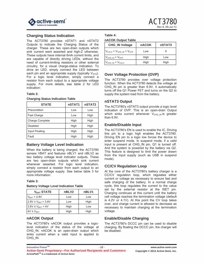
Fix VTHH
Following the same example as above, the "unadjusted" results yield an operating temperature range of -6°C to 33°C vs. the design goal of 0°C to 40°C. In applications that favor VTHH over VTHL, however, one can control the voltage present at TH at low temperatures by connecting a resistor in parallel with ITH. The desired resistance can be found using the following equation:
(ITH + (VCHG_IN - VTHL)/R) × kCOLD(@0°C) × RNOM = VTHL
Rearranging yields
R = (VCHG_IN - VTHL)/(VTHL/(kCOLD(@0°C) × RNOM) - ITH)
R = (5V - 2.5V)/(2.5V/(2.816 × 6.8k ) - 100μA)
R = 82k
Adding 82k in parallel with the current source increases the net current flowing into the thermistor, thus increasing the voltage at TH. Adding this resistance, however, also impacts the upper temperature limit:
VTHH = (ITH + (VCHG_IN - VTHH)/R) × kHOT(@40°C) × RNOM
Rearranging yields,
ACT3780Rev 8, 09-Jul-13
Innovative PowerTM - 11 - www.active-semi.com Copyright © 2013 Active-Semi, Inc. Active-Semi Proprietary For Authorized Recipients and Customers
ActivePathTM is a trademark of Active-Semi.
kHOT(@TC) = VTHH/(RNOM × (ITH + (VCHG_IN - VTHH)/R))
kHOT(@TC) = 0.5V/(6.8k × (100μA + (5V - 0.5V)/82k )) = 0.4748
Reviewing the characteristic curves, the upper threshold is found to move to 45°C, a change of about 14°C. Adding the parallel resistance has allowed us to achieve our desired lower threshold of 0°C with an operating temperature range of 0°C to 45°C, vs. our design target of 0°C to 40°C.
Thermal Regulation and Protection The ACT3780 features an internal thermal regulation loop that reduces the charging current as necessary to ensure that the die temperature does not rise beyond the thermal regulation threshold of 110°C. This feature protects the ACT3780 against excessive junction temperature and makes the device more accommodating to aggressive thermal designs. Note, however, that attention to good thermal designs is required to achieve the fastest possible charge time by maximizing charge current. In order to account for the extended total charge time resulting from operation in thermal regulation mode, the charge timeout periods are extended proportionally to the reduction in charge current. The conditions that cause the ACT3780 to reduce charge current in accordance to the internal thermal regulation loop can be approximated by calculating the power dissipated in the part.
The ACT3780 also features thermal shutdown for further protection. When the device temperature exceeds 160°C, the device will automatically turn off to prevent the IC from damage. After the die temperature decreases below 135°C, the IC will
automatically restart.
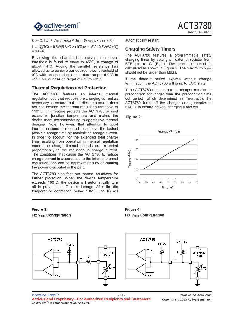
Charging Safety Timers The ACT3780 features a programmable safety charging timer by setting an external resistor from BTR pin to G (RBTR). The time out period is calculated as shown in Figure 2. The maximum RBTR should not be larger than 68k . If the timeout period expires without change termination, the ACT3780 will jump to EOC state.
If the ACT3780 detects that the charger remains in precondition for longer than the precondition time out period (which determined as TNORMAL/3), the ACT3780 turns off the charger and generates a FAULT to ensure prevent charging a bad cell.
Figure 3: Fix VTHL Configuration
Figure 4: Fix VTHH Configuration
Figure 2:
RBTR (k ) 30 35 40 45 50 55 60 65 70
TNORMAL vs. RBTR T N
OR
MA
L (M
in)
190
160
130
100
70
ACT3780Rev 8, 09-Jul-13
Innovative PowerTM - 12 - www.active-semi.com Copyright © 2013 Active-Semi, Inc. Active-Semi Proprietary For Authorized Recipients and Customers
ActivePathTM is a trademark of Active-Semi.
CHG_IN Voltage nACOK
VUVLO < VCHG_IN < VOVP Low
VCHG_IN > VOVP High
VCHG_IN < VUVLO High
nSTAT3
X
Low
High
VBAT STATE nBLV2 nBLV1 VBAT < 2.8V Low Low
2.8V VBAT < 3.6V Low High
3.6V VBAT < 4V High Low
4V VBAT High High
Charging Status Indication The ACT3780 provides nSTAT1 and nSTAT2 Outputs to indicate the Charging Status of the charger. These are two open-drain outputs which sink current went asserted and high-Z otherwise. These outputs have internal 6mA current limits, and are capable of directly driving LEDs, without the need of current-limiting resistors or other external circuitry, for a visual charge-status indication. To drive an LED, simply connect the LED between each pin and an appropriate supply (typically VSYS). For a logic level indication, simply connect a resistor from each output to a appropriate voltage supply. For more details, see table 2 for LED indication:
Table 2: Charging Status Indication Table
Battery Voltage Level Indication When the battery is being charged, the ACT3780 senses VBAT and features nBLV1 and nBLV2 as two battery voltage level indicator outputs. These are two open-drain outputs which sink current whenever asserted. For logic level indication, simply connect a resistor from each output to an appropriate voltage supply. See below table 3 for more information:
Table 3: Battery Voltage Level Indication Table
nACOK Output The ACT3780's nACOK output provides a logic-level indication of the status of the voltage at CHG_IN. nACOK is an open-drain output which sinks current when a valid input is applied to CHG_IN.
Table 4: nACOK Output Table
Over Voltage Protection (OVP) The ACT3780 provides over voltage protection function. When the ACT3780 detects the voltage at CHG_IN pin is greater than 6.9V, it automatically turns off the Q1 Power FET and turns on the Q2 to supply the system load from the battery.
nSTAT3 Output The ACT3780's nSTAT3 output provide a logic level indication of OVP. This is an open-drain Output which sinks current whenever VCHG_IN is greater than 6.9V.
Enable/Disable Input The ACT3780's EN is used to enable the IC. Driving this pin to a logic high enables the ACT3780. Driving EN pin to a logic low forces the device to enter suspend mode. In suspend mode, if a valid input is present at CHG_IN pin, Q1 is turned off. And the system is powered by the battery via Q2. This feature is designed to limit the power drawn from the input supply (such as USB in suspend mode).
CC/CV Regulation Loop At the core of the ACT3780's battery charger is a CC/CV regulation loop, which regulates either current or voltage as necessary to ensure fast and safe charging of the battery. In a normal charge cycle, this loop regulates the current to the value set by the external resistor at the ISET pin. Charging continues at this current until the battery cell voltage reaches the termination voltage (default is 4.2V or 4.1V). At this point the CV loop takes over, and charge current is allowed to decrease as necessary to maintain charging at the termination voltage.
Enable/Disable Charging The ACT3780's DCCC pin can be used to disable charging. By floating the DCCC pin, the charger will be disabled.
STATE nSTAT1 nSTAT2 Precondition Low Low
Fast Charge Low High
Charge Complete High High
Disabled High High
Input Floating High High
Fault High High
ACT3780Rev 8, 09-Jul-13
Innovative PowerTM - 13 - www.active-semi.com Copyright © 2013 Active-Semi, Inc. Active-Semi Proprietary For Authorized Recipients and Customers
ActivePathTM is a trademark of Active-Semi.
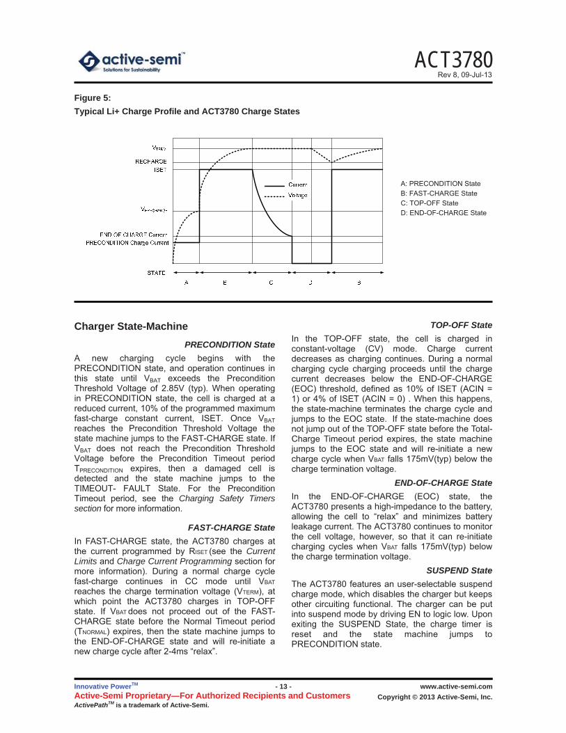
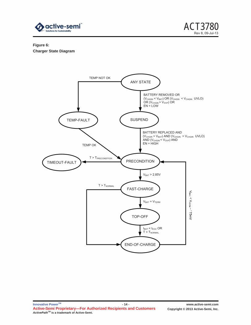
Charger State-Machine PRECONDITION State
A new charging cycle begins with the PRECONDITION state, and operation continues in this state until VBAT exceeds the Precondition Threshold Voltage of 2.85V (typ). When operating in PRECONDITION state, the cell is charged at a reduced current, 10% of the programmed maximum fast-charge constant current, ISET. Once VBAT reaches the Precondition Threshold Voltage the state machine jumps to the FAST-CHARGE state. If VBAT does not reach the Precondition Threshold Voltage before the Precondition Timeout period TPRECONDITION expires, then a damaged cell is detected and the state machine jumps to the TIMEOUT- FAULT State. For the Precondition Timeout period, see the Charging Safety Timers section for more information.
FAST-CHARGE State In FAST-CHARGE state, the ACT3780 charges at the current programmed by RISET (see the Current Limits and Charge Current Programming section for more information). During a normal charge cycle fast-charge continues in CC mode until VBAT reaches the charge termination voltage (VTERM), at which point the ACT3780 charges in TOP-OFF state. If VBAT does not proceed out of the FAST-CHARGE state before the Normal Timeout period (TNORMAL) expires, then the state machine jumps to the END-OF-CHARGE state and will re-initiate a new charge cycle after 2-4ms “relax”.
TOP-OFF StateIn the TOP-OFF state, the cell is charged in constant-voltage (CV) mode. Charge current decreases as charging continues. During a normal charging cycle charging proceeds until the charge current decreases below the END-OF-CHARGE (EOC) threshold, defined as 10% of ISET (ACIN = 1) or 4% of ISET (ACIN = 0) . When this happens, the state-machine terminates the charge cycle and jumps to the EOC state. If the state-machine does not jump out of the TOP-OFF state before the Total-Charge Timeout period expires, the state machine jumps to the EOC state and will re-initiate a new charge cycle when VBAT falls 175mV(typ) below the charge termination voltage.
END-OF-CHARGE StateIn the END-OF-CHARGE (EOC) state, the ACT3780 presents a high-impedance to the battery, allowing the cell to “relax” and minimizes battery leakage current. The ACT3780 continues to monitor the cell voltage, however, so that it can re-initiate charging cycles when VBAT falls 175mV(typ) below the charge termination voltage.
SUSPEND State The ACT3780 features an user-selectable suspend charge mode, which disables the charger but keeps other circuiting functional. The charger can be put into suspend mode by driving EN to logic low. Upon exiting the SUSPEND State, the charge timer is reset and the state machine jumps to PRECONDITION state.
Figure 5: Typical Li+ Charge Profile and ACT3780 Charge States
A: PRECONDITION State B: FAST-CHARGE State C: TOP-OFF State D: END-OF-CHARGE State
ACT3780Rev 8, 09-Jul-13
Innovative PowerTM - 14 - www.active-semi.com Copyright © 2013 Active-Semi, Inc. Active-Semi Proprietary For Authorized Recipients and Customers
ActivePathTM is a trademark of Active-Semi.
Figure 6: Charger State Diagram
SUSPEND
PRECONDITION
FAST-CHARGE
END-OF-CHARGE
BATTERY REMOVED OR(VCHGIN < VBAT) OR (VCHGIN < VCHGIN UVLO)OR (VCHGIN > VOVP) OR EN = LOW
BATTERY REPLACED AND(VCHGIN > VBAT) AND (VCHGIN > VCHGIN UVLO) AND (VCHGIN < VOVP) ANDEN = HIGH
VBAT > 2.85V
VBAT = VTERM
TEMP-FAULT
TOP-OFF
IBAT < IEOC ORT > TNORMAL
TEMP OK
ANY STATETEMP NOT OK
TIMEOUT-FAULTT > TPRECONDITION
T > TNORMAL
ACT3780Rev 8, 09-Jul-13
Innovative PowerTM - 15 - www.active-semi.com Copyright © 2013 Active-Semi, Inc. Active-Semi Proprietary For Authorized Recipients and Customers
ActivePathTM is a trademark of Active-Semi.
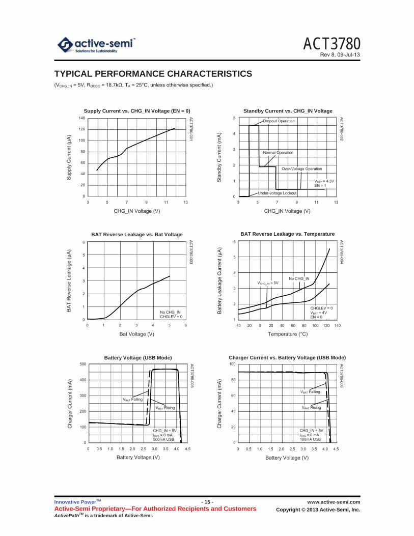
TYPICAL PERFORMANCE CHARACTERISTICS (VCHG_IN = 5V, RDCCC = 18.7k , TA = 25°C, unless otherwise specified.)
CHG_IN Voltage (V)
3 5 7 9 11 13
AC
T3780-001
Supply Current vs. CHG_IN Voltage (EN = 0) 140
120
100
80
60
40
20
0
Sup
ply
Cur
rent
(μA
) A
CT3780-002
Standby Current vs. CHG_IN Voltage
Bat Voltage (V)
0 1 2 3 4 5 6
AC
T3780-003
BAT Reverse Leakage vs. Bat Voltage
AC
T3780-004
BAT Reverse Leakage vs. Temperature
AC
T3780-005
Battery Voltage (USB Mode)
6
5
4
3
2
1
0
Sta
ndby
Cur
rent
(mA
)
BA
T R
ever
se L
eaka
ge (μ
A)
6
5
4
3
2
1
Bat
tery
Lea
kage
Cur
rent
(μA
)
Cha
rger
Cur
rent
(mA
)
Temperature (°C)
-40 -20 0 20 40 60 80 100 120 140
Battery Voltage (V)
0 0.5 1.0 1.5 2.0 2.5 3.0 3.5 4.0 4.5
VBAT = 4.3V EN = 1
No CHG_IN CHGLEV = 0
CHGLEV = 0 VBAT = 4V EN = 0
CHG_IN = 5V ISYS = 0 mA 500mA USB
CHG_IN Voltage (V)
3 5 7 9 11 13
5
4
3
2
1
0
500
400
300
200
100
0
No CHG_IN VCHG_IN = 5V
Battery Voltage (V)
0 0.5 1.0 1.5 2.0 2.5 3.0 3.5 4.0 4.5
AC
T3780-006
Charger Current vs. Battery Voltage (USB Mode)
Cha
rger
Cur
rent
(mA
)
CHG_IN = 5V ISYS = 0 mA 100mA USB
100
80
60
40
20
0
VBAT Falling
VBAT Rising
VBAT Falling
VBAT Rising
Over-Voltage Operation
Normal Operation
Dropout Operation
Under-voltage Lockout
ACT3780Rev 8, 09-Jul-13
Innovative PowerTM - 16 - www.active-semi.com Copyright © 2013 Active-Semi, Inc. Active-Semi Proprietary For Authorized Recipients and Customers
ActivePathTM is a trademark of Active-Semi.
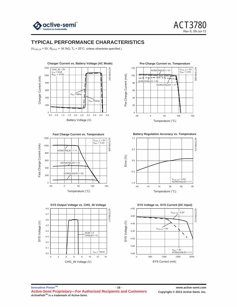
TYPICAL PERFORMANCE CHARACTERISTICS (VCHG_IN = 5V, RDCCC = 18.7k , TA = 25°C, unless otherwise specified.)
Temperature (°C)
-50 0 50 100 150
AC
T3780-008
Pre-Charge Current vs. Temperature
AC
T3780-009
Fast Charge Current vs. Temperature
AC
T3780-010
Battery Regulation Accuracy vs. Temperature
AC
T3780-011
SYS Output Voltage vs. CHG_IN Voltage
AC
T3780-012
SYS Voltage vs. SYS Current (DC Input)
Pre
-Cha
rge
Cur
rent
(mA
)
Fas
t Cha
rge
Cur
rent
(mA
)
1.0
0.5
0.0
-0.5
-1.0
Erro
r (%
)
4.8
4.6
4.5
4.4
4.3
4.2
4.1
4.0
4.7
SYS
Vol
tage
(V)
4.80
4.60
4.40
4.20
4.00
3.80
3.60
SYS
Vol
tage
(V)
Temperature (°C)
-40 -15 10 35 60 85
SYS Current (mA)
0 500 1000 1500 2000
VCHG_IN = 5V VBAT = 2.5V
VBAT = 4V ACIN/CHGLEV = 11
ACIN/CHGLEV = 00
ACIN/CHGLEV = 01
ACIN/CHGLEV = 11
VCHG_IN = 5V VBAT = 3.5V
ACIN/CHGLEV = 00
ACIN/CHGLEV = 01
ACIN/CHGLEV = 11
VCHG_IN = 4.5V ACIN/CHGLEV = 11
VCHG_IN = 5V
VCHG_IN = 5.5V
CHG_IN Voltage (V)
0 2 4 6 8 10 12 14
120
100
80
60
40
20
0
Temperature (°C)
-50 0 50 100 150
1200
1000
800
600
400
200
0
Charger Current vs. Battery Voltage (AC Mode)
AC
T3780-007
1200
1000
800
600
400
200
0
Cha
rger
Cur
rent
(mA
)
CHG_IN = 5V ISYS = 0mA RISET = 510
Battery Voltage (V)
0.0 0.5 1.0 1.5 2.0 2.5 3.0 3.5 4.0 4.5
VBAT Falling
VBAT Rising
ACIN = 0 CHGLEV = 0
ISYS = 10mA
ACT3780Rev 8, 09-Jul-13
Innovative PowerTM - 17 - www.active-semi.com Copyright © 2013 Active-Semi, Inc. Active-Semi Proprietary For Authorized Recipients and Customers
ActivePathTM is a trademark of Active-Semi.
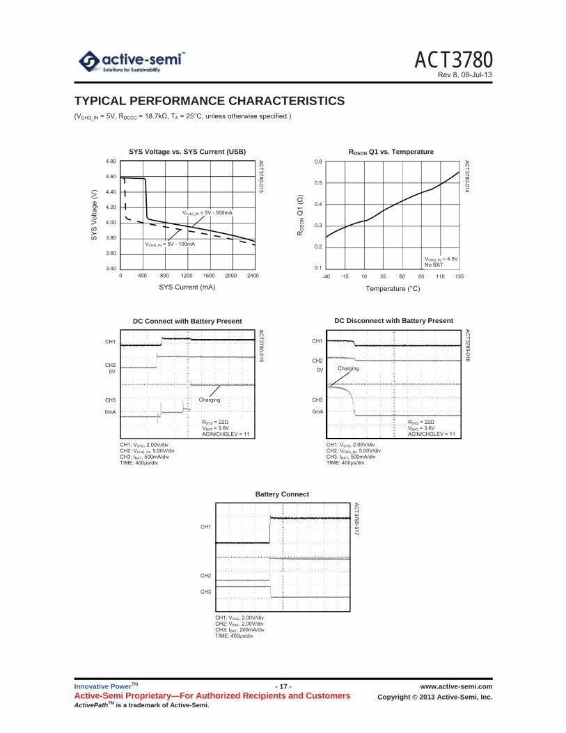
TYPICAL PERFORMANCE CHARACTERISTICS
AC
T3780-013
SYS Voltage vs. SYS Current (USB)
SYS
Vol
tage
(V)
AC
T3780-014
RDSON Q1 vs. Temperature
RD
SO
N Q
1 (
) Temperature (°C)
-40 -15 10 35 60 85 110 135
(VCHG_IN = 5V, RDCCC = 18.7k , TA = 25°C, unless otherwise specified.)
VCHG_IN = 5V - 100mA
VCHG_IN = 5V - 500mA
VCHG_IN = 4.5V No BAT
4.80
4.60
4.40
4.20
4.00
3.80
3.60
3.40
SYS Current (mA)
0 400 800 1200 1600 2000 2400
0.6
0.5
0.4
0.3
0.2
0.1
AC
T3780-015
DC Connect with Battery Present
CH1
CH2
CH3
0mA
CH1: VSYS, 2.00V/div CH2: VCHG_IN, 5.00V/div CH3: IBAT, 500mA/div TIME: 400μs/div
0V
RSYS = 22 VBAT = 3.6V ACIN/CHGLEV = 11
Charging
AC
T3780-016
CH1
CH2
CH3
DC Disconnect with Battery Present
0V
0mA
Charging
RSYS = 22 VBAT = 3.6V ACIN/CHGLEV = 11
CH1: VSYS, 2.00V/div CH2: VCHG_IN, 5.00V/div CH3: IBAT, 500mA/div TIME: 400 s/div
AC
T3780-017
CH1
CH2
CH3
Battery Connect
CH1: VSYS, 2.00V/div CH2: VBAT, 2.00V/div CH3: IBAT, 200mA/div TIME: 400 s/div
ACT3780Rev 8, 09-Jul-13
Innovative PowerTM - 18 - www.active-semi.com Copyright © 2013 Active-Semi, Inc. Active-Semi Proprietary For Authorized Recipients and Customers
ActivePathTM is a trademark of Active-Semi.
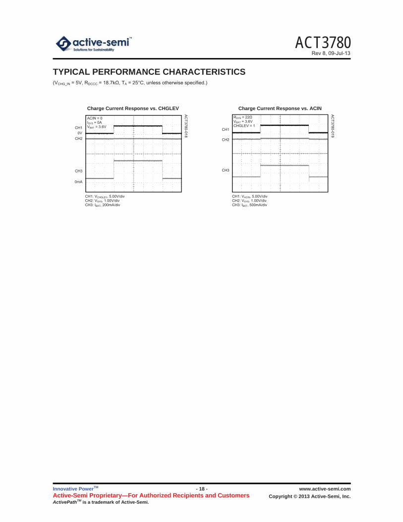
TYPICAL PERFORMANCE CHARACTERISTICS A
CT3780-019
CH1
CH2
CH3
Charge Current Response vs. ACIN
AC
T3780-018
CH1
CH2
CH3
0mA
Charge Current Response vs. CHGLEV
(VCHG_IN = 5V, RDCCC = 18.7k , TA = 25°C, unless otherwise specified.)
RSYS = 22 VBAT = 3.6V CHGLEV = 1
CH1: VACIN, 5.00V/div CH2: VSYS, 1.00V/div CH3: IBAT, 500mA/div
0V
ACIN = 0 ISYS = 0A VBAT = 3.6V
CH1: VCHGLEV, 5.00V/div CH2: VSYS, 1.00V/div CH3: IBAT, 200mA/div
ACT3780Rev 8, 09-Jul-13
Innovative PowerTM - 19 - www.active-semi.com Copyright © 2013 Active-Semi, Inc. Active-Semi Proprietary For Authorized Recipients and Customers
ActivePathTM is a trademark of Active-Semi.
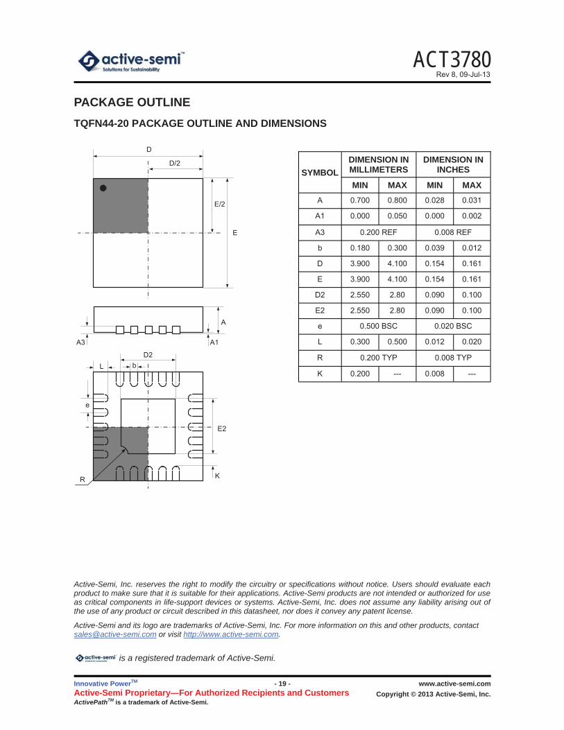
PACKAGE OUTLINE TQFN44-20 PACKAGE OUTLINE AND DIMENSIONS
R
D2
e
bL
D
D/2
E/2
A
A3 A1
E2
K
E
SYMBOL DIMENSION IN MILLIMETERS
DIMENSION IN INCHES
MIN MAX MIN MAX A 0.700 0.800 0.028 0.031
A1 0.000 0.050 0.000 0.002
A3 0.200 REF 0.008 REF
b 0.180 0.300 0.039 0.012
D 3.900 0.154
E 3.900 0.154
D2 2.550 2.80 0.090 0.100
E2 2.550 2.80 0.090 0.100
e 0.500 BSC 0.020 BSC
L 0.300 0.500 0.012 0.020
R 0.200 TYP 0.008 TYP
4.100
4.100
0.161
0.161
K 0.200 0.008 --- ---
Active-Semi, Inc. reserves the right to modify the circuitry or specifications without notice. Users should evaluate each product to make sure that it is suitable for their applications. Active-Semi products are not intended or authorized for use as critical components in life-support devices or systems. Active-Semi, Inc. does not assume any liability arising out of the use of any product or circuit described in this datasheet, nor does it convey any patent license.
Active-Semi and its logo are trademarks of Active-Semi, Inc. For more information on this and other products, contact [email protected] or visit http://www.active-semi.com.
is a registered trademark of Active-Semi.