tms320c28346/28345/28344/28343/28342/28341 … tms320c28346, tms320c28345, tms320c28344...
TRANSCRIPT
TMS320C28346, TMS320C28345, TMS320C28344TMS320C28343, TMS320C28342, TMS320C28341Delfino Microcontrollers
Data Manual
ADVANCE INFORMATION concerns new products in the samplingor preproduction phase of development. Characteristic data andother specifications are subject to change without notice.
Literature Number: SPRS516March 2009

Contents
TMS320C28346, TMS320C28345, TMS320C28344TMS320C28343, TMS320C28342, TMS320C28341Delfino MicrocontrollersSPRS516–MARCH 2009 www.ti.com
1 TMS320C2834x (Delfino™) MCUs........................................................................................... 91.1 Overview ...................................................................................................................... 91.2 Features....................................................................................................................... 91.3 Getting Started.............................................................................................................. 10
2 Introduction ....................................................................................................................... 112.1 Pin Assignments............................................................................................................ 132.2 Signal Descriptions......................................................................................................... 21
3 Functional Overview ........................................................................................................... 323.1 Memory Maps .............................................................................................................. 333.2 Brief Descriptions........................................................................................................... 39
3.2.1 C28x CPU ....................................................................................................... 393.2.2 Memory Bus (Harvard Bus Architecture) .................................................................... 393.2.3 Peripheral Bus .................................................................................................. 393.2.4 Real-Time JTAG and Analysis ................................................................................ 403.2.5 External Interface (XINTF) ..................................................................................... 403.2.6 M0, M1 SARAMs ............................................................................................... 403.2.7 L0, L1, L2, L3, L4, L5, L6, L7, H0, H1, H2, H3, H4, H5 SARAMs ....................................... 403.2.8 Boot ROM ........................................................................................................ 403.2.9 Security ........................................................................................................... 413.2.10 Peripheral Interrupt Expansion (PIE) Block .................................................................. 413.2.11 External Interrupts (XINT1-XINT7, XNMI).................................................................... 413.2.12 Oscillator and PLL .............................................................................................. 423.2.13 Watchdog ........................................................................................................ 423.2.14 Peripheral Clocking ............................................................................................. 423.2.15 Low-Power Modes .............................................................................................. 423.2.16 Peripheral Frames 0, 1, 2, 3 (PFn) ........................................................................... 433.2.17 General-Purpose Input/Output (GPIO) Multiplexer ......................................................... 433.2.18 32-Bit CPU-Timers (0, 1, 2) ................................................................................... 433.2.19 Control Peripherals ............................................................................................. 443.2.20 Serial Port Peripherals ......................................................................................... 44
3.3 Register Map................................................................................................................ 453.4 Device Emulation Registers............................................................................................... 463.5 Interrupts .................................................................................................................... 47
3.5.1 External Interrupts .............................................................................................. 503.6 System Control ............................................................................................................. 51
3.6.1 OSC and PLL Block ............................................................................................ 523.6.1.1 External Reference Oscillator Clock Option....................................................... 533.6.1.2 PLL-Based Clock Module............................................................................ 543.6.1.3 Loss of Input Clock ................................................................................... 55
3.6.2 Watchdog Block ................................................................................................. 553.7 Low-Power Modes Block .................................................................................................. 56
4 Peripherals ........................................................................................................................ 574.1 DMA Overview.............................................................................................................. 574.2 32-Bit CPU-Timers 0/1/2 .................................................................................................. 594.3 Enhanced PWM Modules (ePWM1/2/3/4/5/6/7/8/9) ................................................................... 614.4 High-Resolution PWM (HRPWM) ........................................................................................ 644.5 Enhanced CAP Modules (eCAP1/2/3/4/5/6) ............................................................................ 654.6 Enhanced QEP Modules (eQEP1/2/3) .................................................................................. 674.6.1 External ADC Interface .................................................................................................... 694.7 Multichannel Buffered Serial Port (McBSP) Module ................................................................... 70
Contents2 Submit Documentation Feedback

TMS320C28346, TMS320C28345, TMS320C28344TMS320C28343, TMS320C28342, TMS320C28341
Delfino Microcontrollerswww.ti.com SPRS516–MARCH 2009
4.8 Enhanced Controller Area Network (eCAN) Modules (eCAN-A and eCAN-B)..................................... 734.9 Serial Communications Interface (SCI) Modules (SCI-A, SCI-B, SCI-C) ........................................... 784.10 Serial Peripheral Interface (SPI) Module (SPI-A, SPI-D) ............................................................. 814.11 Inter-Integrated Circuit (I2C) .............................................................................................. 844.12 GPIO MUX .................................................................................................................. 854.13 External Interface (XINTF) ................................................................................................ 92
5 Device Support .................................................................................................................. 945.1 Device and Development Support Tool Nomenclature................................................................ 945.2 Documentation Support ................................................................................................... 96
6 Electrical Specifications .................................................................................................... 1006.1 Absolute Maximum Ratings ............................................................................................. 1006.2 Recommended Operating Conditions.................................................................................. 1016.3 Electrical Characteristics ................................................................................................ 1016.4 Current Consumption..................................................................................................... 102
6.4.1 Reducing Current Consumption ............................................................................. 1036.5 Thermal Design Considerations ........................................................................................ 1056.6 Emulator Connection Without Signal Buffering for the MCU........................................................ 1056.7 Timing Parameter Symbology........................................................................................... 106
6.7.1 General Notes on Timing Parameters....................................................................... 1066.7.2 Test Load Circuit .............................................................................................. 1066.7.3 Device Clock Table ........................................................................................... 107
6.8 Clock Requirements and Characteristics ............................................................................. 1086.9 Power Sequencing........................................................................................................ 109
6.9.1 Power Management and Supervisory Circuit Solutions................................................... 1096.10 General-Purpose Input/Output (GPIO)................................................................................. 112
6.10.1 GPIO - Output Timing ......................................................................................... 1126.10.2 GPIO - Input Timing ........................................................................................... 1136.10.3 Sampling Window Width for Input Signals.................................................................. 1146.10.4 Low-Power Mode Wakeup Timing........................................................................... 115
6.11 Enhanced Control Peripherals .......................................................................................... 1186.11.1 Enhanced Pulse Width Modulator (ePWM) Timing........................................................ 1186.11.2 Trip-Zone Input Timing ........................................................................................ 118
6.12 External Interrupt Timing................................................................................................. 1206.13 I2C Electrical Specification and Timing ................................................................................ 1216.14 Serial Peripheral Interface (SPI) Timing ............................................................................... 121
6.14.1 Master Mode Timing........................................................................................... 1216.14.2 SPI Slave Mode Timing ....................................................................................... 125
6.15 External Interface (XINTF) Timing...................................................................................... 1276.15.1 USEREADY = 0 ................................................................................................ 1286.15.2 Synchronous Mode (USEREADY = 1, READYMODE = 0) .............................................. 1286.15.3 Asynchronous Mode (USEREADY = 1, READYMODE = 1) ............................................. 1296.15.4 XINTF Signal Alignment to XCLKOUT ...................................................................... 1306.15.5 External Interface Read Timing .............................................................................. 1316.15.6 External Interface Write Timing .............................................................................. 1326.15.7 External Interface Ready-on-Read Timing With One External Wait State ............................. 1346.15.8 External Interface Ready-on-Write Timing With One External Wait State.............................. 1376.15.9 XHOLD and XHOLDA Timing ................................................................................ 140
6.16 Multichannel Buffered Serial Port (McBSP) Timing .................................................................. 1426.16.1 McBSP Transmit and Receive Timing ...................................................................... 1426.16.2 McBSP as SPI Master or Slave Timing ..................................................................... 145
7 Thermal/Mechanical Data................................................................................................... 149
Contents 3
TMS320C28346, TMS320C28345, TMS320C28344TMS320C28343, TMS320C28342, TMS320C28341Delfino MicrocontrollersSPRS516–MARCH 2009 www.ti.com
List of Figures2-1 C2834x 179-Ball ZHH MicroStar BGA™ Upper Left Quadrant (Bottom VIew) ........................................... 13
2-2 C2834x 179-Ball ZHH MicroStar BGA™ Upper Right Quadrant (Bottom View).......................................... 14
2-3 C2834x 179-Ball ZHH MicroStar BGA™ Lower Left Quadrant (Bottom View) ........................................... 15
2-4 C2834x 179-Ball ZHH MicroStar BGA™ Lower Right Quadrant (Bottom View).......................................... 16
2-5 C2834x 256-Ball ZFE Plastic BGA Upper Left Quadrant (Bottom View) .................................................. 17
2-6 C2834x 256-Ball ZFE Plastic BGA Upper Right Quadrant (Bottom View) ................................................ 18
2-7 C2834x 256-Ball ZFE Plastic BGA Lower Left Quadrant (Bottom View) .................................................. 19
2-8 C2834x 256-Ball ZFE Plastic BGA Lower Right Quadrant (Bottom View) ................................................ 20
3-1 Functional Block Diagram ....................................................................................................... 32
3-2 C28346/C28345 Memory Map .................................................................................................. 34
3-3 C28344/C28343 Memory Map .................................................................................................. 35
3-4 C28342, C28341 Memory Map.................................................................................................. 36
3-5 External and PIE Interrupt Sources............................................................................................. 47
3-6 External Interrupts ................................................................................................................ 48
3-7 Multiplexing of Interrupts Using the PIE Block ................................................................................ 49
3-8 Clock and Reset Domains ....................................................................................................... 51
3-9 OSC and PLL Block Diagram ................................................................................................... 52
3-10 Using a 3.3-V External Oscillator ............................................................................................... 53
3-11 Using a 1.8-V External Oscillator ............................................................................................... 53
3-12 Using the Internal Oscillator ..................................................................................................... 53
3-13 Watchdog Module................................................................................................................. 55
4-1 DMA Functional Block Diagram ................................................................................................. 58
4-2 CPU-Timers........................................................................................................................ 59
4-3 CPU-Timer Interrupt Signals and Output Signal .............................................................................. 59
4-4 Generation of SOC Pulses to the External ADC Module ................................................................... 61
4-5 ePWM Submodules Showing Critical Internal Signal Interconnections.................................................... 64
4-6 eCAP Functional Block Diagram ................................................................................................ 65
4-7 eQEP Functional Block Diagram................................................................................................ 67
4-8 External ADC Interface ........................................................................................................... 69
4-9 McBSP Module ................................................................................................................... 71
4-10 eCAN Block Diagram and Interface Circuit .................................................................................... 74
4-11 eCAN-A Memory Map ............................................................................................................ 75
4-12 eCAN-B Memory Map ............................................................................................................ 76
4-13 Serial Communications Interface (SCI) Module Block Diagram ............................................................ 80
4-14 SPI Module Block Diagram (Slave Mode) ..................................................................................... 83
4-15 I2C Peripheral Module Interfaces ............................................................................................... 84
4-16 GPIO MUX Block Diagram....................................................................................................... 86
4-17 Qualification Using Sampling Window.......................................................................................... 91
4-18 External Interface Block Diagram ............................................................................................... 92
List of Figures4 Submit Documentation Feedback

TMS320C28346, TMS320C28345, TMS320C28344TMS320C28343, TMS320C28342, TMS320C28341
Delfino Microcontrollerswww.ti.com SPRS516–MARCH 2009
4-19 Typical 16-bit Data Bus XINTF Connections .................................................................................. 92
4-20 Typical 32-bit Data Bus XINTF Connections .................................................................................. 93
5-1 Example of C2834x Device Nomenclature .................................................................................... 95
6-1 Emulator Connection Without Signal Buffering for the MCU............................................................... 105
6-2 3.3-V Test Load Circuit ......................................................................................................... 106
6-3 Clock Timing ..................................................................................................................... 109
6-4 Power-on Reset.................................................................................................................. 110
6-5 Warm Reset ...................................................................................................................... 111
6-6 Example of Effect of Writing Into PLLCR Register .......................................................................... 112
6-7 General-Purpose Output Timing............................................................................................... 112
6-8 Sampling Mode .................................................................................................................. 113
6-9 General-Purpose Input Timing ................................................................................................. 114
6-10 IDLE Entry and Exit Timing .................................................................................................... 115
6-11 STANDBY Entry and Exit Timing Diagram................................................................................... 116
6-12 HALT Wake-Up Using GPIOn ................................................................................................. 117
6-13 PWM Hi-Z Characteristics ...................................................................................................... 118
6-14 ADCSOCAO or ADCSOCBO Timing ......................................................................................... 120
6-15 External Interrupt Timing ....................................................................................................... 120
6-16 SPI Master Mode External Timing (Clock Phase = 0) ...................................................................... 123
6-17 SPI Master Mode External Timing (Clock Phase = 1) ...................................................................... 125
6-18 SPI Slave Mode External Timing (Clock Phase = 0)........................................................................ 126
6-19 SPI Slave Mode External Timing (Clock Phase = 1)........................................................................ 127
6-20 Relationship Between XTIMCLK and SYSCLKOUT ........................................................................ 130
6-21 Example Read Access .......................................................................................................... 132
6-22 Example Write Access .......................................................................................................... 133
6-23 Example Read With Synchronous XREADY Access ....................................................................... 135
6-24 Example Read With Asynchronous XREADY Access ...................................................................... 136
6-25 Write With Synchronous XREADY Access................................................................................... 138
6-26 Write With Asynchronous XREADY Access ................................................................................. 139
6-27 External Interface Hold Waveform ............................................................................................ 141
6-28 McBSP Receive Timing......................................................................................................... 144
6-29 McBSP Transmit Timing ........................................................................................................ 144
6-30 McBSP Timing as SPI Master or Slave: CLKSTP = 10b, CLKXP = 0.................................................... 145
6-31 McBSP Timing as SPI Master or Slave: CLKSTP = 11b, CLKXP = 0.................................................... 146
6-32 McBSP Timing as SPI Master or Slave: CLKSTP = 10b, CLKXP = 1.................................................... 147
6-33 McBSP Timing as SPI Master or Slave: CLKSTP = 11b, CLKXP = 1.................................................... 148
List of Figures 5

TMS320C28346, TMS320C28345, TMS320C28344TMS320C28343, TMS320C28342, TMS320C28341Delfino MicrocontrollersSPRS516–MARCH 2009 www.ti.com
List of Tables2-1 C2834x Hardware Features ..................................................................................................... 12
2-2 Signal Descriptions ............................................................................................................... 21
3-1 Wait-states ......................................................................................................................... 38
3-2 Boot Mode Selection.............................................................................................................. 40
3-3 Peripheral Frame 0 Registers .................................................................................................. 45
3-4 Peripheral Frame 1 Registers ................................................................................................... 45
3-5 Peripheral Frame 2 Registers ................................................................................................... 46
3-6 Peripheral Frame 3 Registers ................................................................................................... 46
3-7 Device Emulation Registers ..................................................................................................... 46
3-8 PIE Peripheral Interrupts ........................................................................................................ 49
3-9 PIE Configuration and Control Registers ...................................................................................... 50
3-10 External Interrupt Registers...................................................................................................... 50
3-11 PLL, Clocking, Watchdog, and Low-Power Mode Registers ................................................................ 52
3-12 PLL Settings ....................................................................................................................... 54
3-13 CLKIN Divide Options ............................................................................................................ 54
3-14 Possible PLL Configuration Modes ............................................................................................. 55
3-15 Low-Power Modes ................................................................................................................ 56
4-1 CPU-Timers 0, 1, 2 Configuration and Control Registers ................................................................... 60
4-2 ePWM1-4 Control and Status Registers ....................................................................................... 62
4-3 ePWM5-9 Control and Status Registers ....................................................................................... 63
4-4 eCAP Control and Status Registers ............................................................................................ 66
4-5 eQEP Control and Status Registers ............................................................................................ 68
4-6 External ADC Interface Registers .............................................................................................. 69
4-7 McBSP Register Summary ...................................................................................................... 72
4-8 3.3-V eCAN Transceivers ....................................................................................................... 74
4-9 CAN Register Map ............................................................................................................... 77
4-10 SCI-A Registers .................................................................................................................. 79
4-11 SCI-B Registers .................................................................................................................. 79
4-12 SCI-C Registers .................................................................................................................. 79
4-13 SPI-A Registers ................................................................................................................... 82
4-14 SPI-D Registers ................................................................................................................... 82
4-15 I2C-A Registers.................................................................................................................... 85
4-16 GPIO Registers ................................................................................................................... 87
4-17 GPIO-A Mux Peripheral Selection Matrix ..................................................................................... 88
4-18 GPIO-B Mux Peripheral Selection Matrix ..................................................................................... 89
4-19 GPIO-C Mux Peripheral Selection Matrix ..................................................................................... 90
4-20 XINTF Configuration and Control Register Mapping ......................................................................... 93
5-1 TMS320x2834x Delfino Peripheral Selection Guide ......................................................................... 96
6-1 TMS320C28346/C28344/C28342 Current Consumption by Power-Supply Pins at 300-MHz SYSCLKOUT ....... 102
List of Tables6 Submit Documentation Feedback

TMS320C28346, TMS320C28345, TMS320C28344TMS320C28343, TMS320C28342, TMS320C28341
Delfino Microcontrollerswww.ti.com SPRS516–MARCH 2009
6-2 TMS320C28345/C28343/C28341 Current Consumption by Power-Supply Pins at 200-MHz SYSCLKOUT ....... 103
6-3 Typical Current Consumption by Various Peripherals ..................................................................... 104
6-4 Clocking and Nomenclature (300-MHz devices) ............................................................................ 107
6-5 Clocking and Nomenclature (200-MHz devices) ............................................................................ 107
6-6 Input Clock Frequency .......................................................................................................... 108
6-7 XCLKIN Timing Requirements - PLL Enabled............................................................................... 108
6-8 XCLKIN Timing Requirements - PLL Disabled .............................................................................. 108
6-9 XCLKOUT Switching Characteristics (PLL Bypassed or Enabled) ....................................................... 108
6-10 Reset (XRS) Timing Requirements ........................................................................................... 111
6-11 General-Purpose Output Switching Characteristics......................................................................... 112
6-12 General-Purpose Input Timing Requirements ............................................................................... 113
6-13 IDLE Mode Timing Requirements ............................................................................................. 115
6-14 IDLE Mode Switching Characteristics......................................................................................... 115
6-15 STANDBY Mode Timing Requirements ...................................................................................... 115
6-16 STANDBY Mode Switching Characteristics ................................................................................. 116
6-17 HALT Mode Timing Requirements ............................................................................................ 116
6-18 HALT Mode Switching Characteristics ....................................................................................... 117
6-19 ePWM Timing Requirements................................................................................................... 118
6-20 ePWM Switching Characteristics .............................................................................................. 118
6-21 Trip-Zone input Timing Requirements ........................................................................................ 118
6-22 High Resolution PWM Characteristics at SYSCLKOUT = (150 - 300 MHz) ............................................. 119
6-23 Enhanced Capture (eCAP) Timing Requirement............................................................................ 119
6-24 eCAP Switching Characteristics ............................................................................................... 119
6-25 Enhanced Quadrature Encoder Pulse (eQEP) Timing Requirements.................................................... 119
6-26 eQEP Switching Characteristics ............................................................................................... 119
6-27 External ADC Start-of-Conversion Switching Characteristics.............................................................. 119
6-28 External Interrupt Timing Requirements ...................................................................................... 120
6-29 External Interrupt Switching Characteristics ................................................................................. 120
6-30 I2C Timing ....................................................................................................................... 121
6-31 SPI Master Mode External Timing (Clock Phase = 0) ...................................................................... 122
6-32 SPI Master Mode External Timing (Clock Phase = 1) ...................................................................... 124
6-33 SPI Slave Mode External Timing (Clock Phase = 0)........................................................................ 125
6-34 SPI Slave Mode External Timing (Clock Phase = 1)........................................................................ 126
6-35 Relationship Between Parameters Configured in XTIMING and Duration of Pulse .................................... 127
6-36 XINTF Clock Configurations.................................................................................................... 130
6-37 External Interface Read Timing Requirements .............................................................................. 131
6-38 External Interface Read Switching Characteristics.......................................................................... 131
6-39 External Interface Write Switching Characteristics.......................................................................... 132
6-40 External Interface Read Switching Characteristics (Ready-on-Read, 1 Wait State).................................... 134
6-41 External Interface Read Timing Requirements (Ready-on-Read, 1 Wait State) ........................................ 134
6-42 Synchronous XREADY Timing Requirements (Ready-on-Read, 1 Wait State) ......................................... 134
List of Tables 7

TMS320C28346, TMS320C28345, TMS320C28344TMS320C28343, TMS320C28342, TMS320C28341Delfino MicrocontrollersSPRS516–MARCH 2009 www.ti.com
6-43 Asynchronous XREADY Timing Requirements (Ready-on-Read, 1 Wait State)........................................ 134
6-44 External Interface Write Switching Characteristics (Ready-on-Write, 1 Wait State) .................................... 137
6-45 Synchronous XREADY Timing Requirements (Ready-on-Write, 1 Wait State) ......................................... 137
6-46 Asynchronous XREADY Timing Requirements (Ready-on-Write, 1 Wait State)........................................ 137
6-47 XHOLD/XHOLDA Timing Requirements ..................................................................................... 140
6-48 McBSP Timing Requirements.................................................................................................. 142
6-49 McBSP Switching Characteristics ............................................................................................. 143
6-50 McBSP as SPI Master or Slave Timing Requirements (CLKSTP = 10b, CLKXP = 0) ................................. 145
6-51 McBSP as SPI Master or Slave Switching Characteristics (CLKSTP = 10b, CLKXP = 0)............................. 145
6-52 McBSP as SPI Master or Slave Timing Requirements (CLKSTP = 11b, CLKXP = 0) ................................. 146
6-53 McBSP as SPI Master or Slave Switching Characteristics (CLKSTP = 11b, CLKXP = 0)............................. 146
6-54 McBSP as SPI Master or Slave Timing Requirements (CLKSTP = 10b, CLKXP = 1) ................................. 147
6-55 McBSP as SPI Master or Slave Switching Characteristics (CLKSTP = 10b, CLKXP = 1)............................. 147
6-56 McBSP as SPI Master or Slave Timing Requirements (CLKSTP = 11b, CLKXP = 1) ................................. 148
6-57 McBSP as SPI Master or Slave Switching Characteristics (CLKSTP = 11b, CLKXP = 1)............................. 148
7-1 Thermal Model 179-Ball ZHH Results ........................................................................................ 149
7-2 Thermal Model 256-Ball ZFE Results ........................................................................................ 149
List of Tables8 Submit Documentation Feedback

AD
VAN
CE
INF
OR
MA
TIO
N
1 TMS320C2834x (Delfino™) MCUs
1.1 Overview
1.2 Features
TMS320C28346, TMS320C28345, TMS320C28344TMS320C28343, TMS320C28342, TMS320C28341
Delfino Microcontrollerswww.ti.com SPRS516–MARCH 2009
The TMS320C2834x (C2834x) Delfino™ microcontroller (MCU) devices build on TI's existing F2833xhigh-performance floating-point microcontrollers. The C2834x delivers up to 300 MHz of floating-pointperformance, up to 516KB of single-access RAM, and PWM modules with 65 picoseconds of resolution.Designed for real-time control applications, the C2834x is based on the C28x™ core, making itcode-compatible with all C28x microcontrollers. The on-chip peripherals and low-latency core make theC2834x an excellent solution for performance-hungry real-time control applications.
• Dead-Band Generation• High-Performance Static CMOS Technology• PWM Chopping by High-Frequency– Up to 300 MHz (3.33-ns Cycle Time)
Carrier– 1.1-V/1.2-V Core, 3.3-V I/O, 1.8-V• Trip Zone InputPLL/Oscillator Design• Up to 9 HRPWM Outputs With 60 ps• High-Performance 32-Bit CPU (TMS320C28x)
MEP Resolution– IEEE-754 Single-Precision Floating-Point– Six 32-bit Enhanced Capture (eCAP)Unit (FPU)
Modules– 16 x 16 and 32 x 32 MAC Operations• Configurable as 3 Capture Inputs or– 16 x 16 Dual MAC 3 Auxiliary Pulse With Modulator
– Harvard Bus Architecture Outputs– Fast Interrupt Response and Processing • Single-Shot Capture of up to Four Event– Code-Efficient (in C/C++ and Assembly) Time-Stamps
• Six Channel DMA Controller (for McBSP, – Three 32-bit Quadrature Encoder Pulse(QEP) ModulesXINTF, and SARAM)
– Six 32-bit Timers/Nine 16-bit Timers• 16-bit or 32-bit External Interface (XINTF)• Three 32-Bit CPU Timers– Over 2M x 16 Address Reach• Serial Port Peripherals• On-Chip Memory
– Up to 2 CAN Modules– Up to 258K x 16 SARAM– Up to 3 SCI (UART) Modules– 8K x 16 Boot ROM– Up to 2 McBSP Modules (Configurable as• Clock and System Control
SPI)– Dynamic PLL Ratio Changes Supported– Up to 2 SPI Modules– On-Chip Oscillator– One Inter-Integrated-Circuit (I2C) Bus– Watchdog Timer Module
• External ADC Interface• Peripheral Interrupt Expansion (PIE) Block• Up to 88 Individually Programmable,That Supports All 64 Peripheral Interrupts
Multiplexed GPIO Pins With Input Filtering• Enhanced Control Peripherals• Advanced Emulation Features– Eighteen Enhanced Pulse Width Modulator
– Analysis and Breakpoint Functions(ePWM) Outputs– Real-Time Debug via Hardware• Dedicated 16-bit Time-Based Counter
With Period and Frequency Control • 2834x Package Options:• Single-Edge, Dual-Edge Symmetric, or – MicroStar BGA™ (ZHH)
Dual-Edge Asymmetric Outputs – Plastic BGA (ZFE)
Please be aware that an important notice concerning availability, standard warranty, and use in critical applications of TexasInstruments semiconductor products and disclaimers thereto appears at the end of this document.
Delfino, C28x, MicroStar BGA, TMS320C28x, TMS320C54x, TMS320C55x, Code Composer Studio are trademarks of Texas Instruments.All other trademarks are the property of their respective owners.
ADVANCE INFORMATION concerns new products in the sampling Copyright © 2009, Texas Instruments Incorporatedor preproduction phase of development. Characteristic data andother specifications are subject to change without notice.

AD
VAN
CE
INF
OR
MA
TIO
N
1.3 Getting Started
TMS320C28346, TMS320C28345, TMS320C28344TMS320C28343, TMS320C28342, TMS320C28341Delfino MicrocontrollersSPRS516–MARCH 2009 www.ti.com
This section gives a brief overview of the steps to take when first developing for a C28x device. For moredetail on each of these steps, see the following:• Getting Started With TMS320C28x™ Digital Signal Controllers (literature number SPRAAM0).• C2000 Getting Started Website (http://www.ti.com/c2000getstarted)• TMS320F28x Development and Experimenter's Kits (http://www.ti.com/f28xkits)
TMS320C2834x (Delfino™) MCUs10 Submit Documentation Feedback

AD
VAN
CE
INF
OR
MA
TIO
N
2 Introduction
TMS320C28346, TMS320C28345, TMS320C28344TMS320C28343, TMS320C28342, TMS320C28341
Delfino Microcontrollerswww.ti.com SPRS516–MARCH 2009
The TMS320C28346, TMS320C28345, TMS320C28344, TMS320C28343, TMS320C28342, andTMS320C28341 devices, members of the TMS320C28x™ MCU generation, are highly integrated,high-performance solutions for demanding control applications.
Throughout this document, the devices are abbreviated as C28346, C28345, C28344, C28343, C28342,and C28341, respectively. Table 2-1 provides a summary of features for each device.
Submit Documentation Feedback Introduction 11

TMS320C28346, TMS320C28345, TMS320C28344TMS320C28343, TMS320C28342, TMS320C28341Delfino MicrocontrollersSPRS516–MARCH 2009 www.ti.com
Table 2-1. C2834x Hardware FeaturesC28346 (2) C28345 C28344 C28343(2) C28342 C28341FEATURE TYPE (1)(300 MHz) (200 MHz) (300 MHz) (200 MHz) (300 MHz) (200 MHz)
256-Ball ZFE 256-Ball ZFE 179-Ball ZHH 256-Ball ZFE 256-Ball ZFE 179-Ball ZHH 256-Ball ZFE 256-Ball ZFE 179-Ball ZHHPackage Type – PBGA (3) PBGA(3) BGA PBGA(3) PBGA(3) BGA PBGA(3) PBGA(3) BGA
Instruction cycle – 3.33 ns 5 ns 3.33 ns 5 ns 3.33 ns 5 ns
Floating-point unit – Yes Yes Yes Yes Yes Yes
Single-access RAM (SARAM) (16-bit word) – 258K 258K 130K 130K 98K 98K
Code security for on-chip SARAM blocks – No (4) No(4) No(4) No(4) No(4) No(4)
Boot ROM (8K x 16) – Yes Yes Yes Yes Yes Yes
16-/32-bit External Interface (XINTF) 1 Yes Yes Yes Yes Yes Yes
6-channel Direct Memory Access (DMA) 0 Yes Yes Yes Yes Yes Yes
ePWM1/2/3/ ePWM1/2/3/ ePWM1/2/3/ ePWM1/2/3/ ePWM1/2/3/ ePWM1/2/3/PWM outputs 0 4/5/6/7/8/9 4/5/6/7/8/9 4/5/6/7/8/9 4/5/6/7/8/9 4/5/6 4/5/6
ePWM1A/2A/ ePWM1A/2A/ ePWM1A/2A/ ePWM1A/2A/ ePWM1A/2A/ ePWM1A/2A/HRPWM channels 0 3A/4A/5A/6A/ 3A/4A/5A/6A/ 3A/4A/5A/6A/ 3A/4A/5A/6A/ 3A/4A/5A/6A 3A/4A/5A/6A7A/8A/9A 7A/8A/9A 7A/8A/9A 7A/8A/9A
32-bit Capture inputs or auxiliary PWM outputs 0 6 6 6 6 4 4
32-bit QEP channels (four inputs/channel) 0 3 3 3 3 2 2
Watchdog timer – Yes Yes Yes Yes Yes Yes
External ADC Interface – Yes Yes Yes Yes Yes Yes
32-bit CPU timers – 3 3 3 3 3 3
Multichannel Buffered Serial Port (McBSP)/SPI 1 2 2 2 2 1 1
Serial Peripheral Interface (SPI) 0 2 2 2 2 2 2
Serial Communications Interface (SCI) 0 3 3 3 3 3 3
Enhanced Controller Area Network (eCAN) 0 2 2 2 2 2 2
Inter-Integrated Circuit (I2C) 0 1 1 1 1 1 1
General-Purpose Input/Output (GPIO) pins – 88 88 88 88 88 88(shared)
External interrupts – 8 8 8 8 8 8
Temperature T: - 40°C to 105°C – ZFE ZFE ZHH ZFE ZFE ZHH ZFE ZFE ZHHoptions
Product status (5) – TMX TMX TMX TMX TMX TMX
(1) A type change represents a major functional feature difference in a peripheral module. Within a peripheral type, there may be minor differences between devices that do not affectthe basic functionality of the module. These device-specific differences are listed in the TMS320x28xx, 28xxx DSP Peripheral Reference Guide (SPRU566) and in the peripheralreference guides.
(2) During TMX, only C28346 and C28343 devices will be sampled. Other device configurations will be available later. For initial development, customers should use the C28346 andC28343 devices.
(3) Initial samples will come with the ZEP designator. The designator will change to ZFE in production.(4) Custom secure versions of these devices are available. See Section 3.2.9, Security, for more details.(5) See Section 5.1 for descriptions of device stages.
12 Introduction Submit Documentation Feedback

AD
VAN
CE
INF
OR
MA
TIO
N
2.1 Pin Assignments
EXTSOC3B
GPIO19/
/
SCIRXDB/
CANTXA
SPISTEA
GPIO23/
EQEP1I/
MFSXA/
SCIRXDB
GPIO24/
ECAP1/
EQEP2A/
MDXB
EXTSOC1A
EXTSOC2A EXTSOC1B
GPIO21/
EQEP1B/
MDRA/
CANRXB
GPIO20/
EQEP1A/
MDXA/
CANTXB
P P
N N
M M
L L
GPIO18/
SPICLKA/
SCITXDB/
CANRXA
TDI
GPIO16/
SPISIMOA/
CANTXB/
TZ5
GPIO12/
/
CANTXB/
MDXB
TZ1
EXTSOC3A
K K
J J
H H
1 2 3 4 5
6 7
TDO
VSS
1 2 3 4 5 6 7
EXTSOC2B
TRST
GPIO17/
SPISOMIA/
CANRXB/
TZ6
GPIO13/
/
CANRXB/
MDRB
TZ2
GPIO15/
/ /
SCIRXDB/
MFSXB
TZ4 XHOLDA
GPIO25/
ECAP2/
EQEP2B/
MDRB
GPIO22/
EQEP1S/
MCLKXA/
SCITXDB
EXTADCCLK
VDD
VSS
VSS
VDDIO
VDDIO
VSS
GPIO11/
EPWM6B/
SCIRXDB/
ECAP4
VDD
VDD
VDD
VSS
VDDIO
GPIO14/
/ /
SCITXDB/
MCLKXB
TZ3 XHOLD
VDD
VDD
VSS
VDDIO
GPIO26/
ECAP3/
EQEP2I/
MCLKXB
GPIO27/
ECAP4/
EQEP2S/
MFSXB
GPIO33/
SCLA/
EPWMSYNCO/
ADCSOCBO
GPIO32/
SDAA/
EPWMSYNCI/
ADCSOCAO
TMS320C28346, TMS320C28345, TMS320C28344TMS320C28343, TMS320C28342, TMS320C28341
Delfino Microcontrollerswww.ti.com SPRS516–MARCH 2009
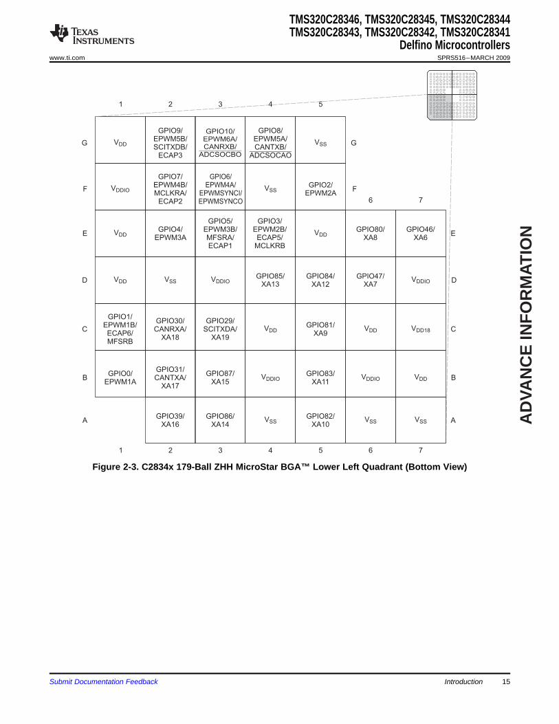
The 179-ball ZHH ball grid array (BGA) terminal assignments are shown in Figure 2-1 through Figure 2-4.The 256-ball ZFE plastic ball grid array (PBGA) terminal assignments are shown in Figure 2-5 throughFigure 2-8. Table 2-2 describes the function(s) of each pin.
Figure 2-1. C2834x 179-Ball ZHH MicroStar BGA™ Upper Left Quadrant (Bottom VIew)
Submit Documentation Feedback Introduction 13

AD
VAN
CE
INF
OR
MA
TIO
N
GPIO49/
ECAP6/
XD30/
SPISOMID
VDDIO
GPIO54/
SPISIMOA/
XD25/
EQEP3A
GPIO59/
MFSRA/
XD20/
EPWM7B
GPIO55/
SPISOMIA/
XD24/
EQEP3B
GPIO60/
MCLKRB/
XD19/
EPWM8A
VSS
EMU1
GPIO /
MFSRB/
XD18/
EPWM8B
61
GPIO70/
XD9
TCK
VDD
EMU0
8 9
10 11 12 13 14
PP
NN
MM
LL
KK
JJ
HH
GPIO63/
SCITXDC/
XD16/
EPWM9B
GPIO68/
XD11
VSS
XRSIO
GPIO65/
XD14
VSS
8 9 10 11 12 13 14
XRS
VSS
TMS
VDD
GPIO67/
XD12
GPIO66/
XD13
GPIO62/
SCIRXDC/
XD17/
EPWM9A
VDD
GPIO57/
/
XD22/
EQEP3I
SPISTEA
GPIO50/
EQEP1A/
XD29/
SPICLKD
GPIO51/
EQEP1B/
XD28/
SPISTED
VSS
VDDIO
VDD VSS VDD
GPIO64/
XD15
GPIO48/
ECAP5/
XD31/
SPISIMOD
GPIO52/
EQEP1S/
XD27
GPIO53/
EQEP1I/
XD26
GPIO56/
SPICLKA/
XD23/
EQEP3S
GPIO58/
MCLKRA/
XD21/
EPWM7A
VDDIO
VDDIO
VDD
GPIO69/
XD10
TMS320C28346, TMS320C28345, TMS320C28344TMS320C28343, TMS320C28342, TMS320C28341Delfino MicrocontrollersSPRS516–MARCH 2009 www.ti.com
Figure 2-2. C2834x 179-Ball ZHH MicroStar BGA™ Upper Right Quadrant (Bottom View)
14 Introduction Submit Documentation Feedback
AD
VAN
CE
INF
OR
MA
TIO
N
GPIO9/
EPWM5B/
SCITXDB/
ECAP3
GPIO10/
EPWM6A/
CANRXB/
ADCSOCBO
GPIO8/
EPWM5A/
CANTXB/
ADCSOCAO
VSS
GPIO80/
XA8
GPIO7/
EPWM4B/
MCLKRA/
ECAP2
VDDGPIO4/
EPWM3A
GPIO5/
EPWM3B/
MFSRA/
ECAP1
GPIO3/
EPWM2B/
ECAP5/
MCLKRB
GPIO46/
XA6
VDD VSS VDDIOGPIO85/
XA13
GPIO84/
XA12
G
F
E
D
GPIO1/
EPWM1B/
ECAP6/
MFSRB
GPIO30/
CANRXA/
XA18
GPIO29/
SCITXDA/
XA19
VDDGPIO81/
XA9
GPIO0/
EPWM1A
GPIO31/
CANTXA/
XA17
GPIO87/
XA15VDDIO
GPIO83/
XA11
GPIO39/
XA16
GPIO86/
XA14VSS
C
B
A
1 2 3 4 5 6 7
G
F
E
D
C
B
A
VDD18VDD
VDDIO VDD
VSSVSSGPIO82/
XA10
1 2 3 4 5
6 7
VSS
VDD
VDDIO
GPIO6/
EPWM4A/
EPWMSYNCI/
EPWMSYNCO
GPIO2/
EPWM2A
VDD
GPIO47/
XA7VDDIO
TMS320C28346, TMS320C28345, TMS320C28344TMS320C28343, TMS320C28342, TMS320C28341
Delfino Microcontrollerswww.ti.com SPRS516–MARCH 2009
Figure 2-3. C2834x 179-Ball ZHH MicroStar BGA™ Lower Left Quadrant (Bottom View)
Submit Documentation Feedback Introduction 15

AD
VAN
CE
INF
OR
MA
TIO
N
GPIO71/
XD8
GPIO72/
XD7
GPIO73/
XD6
GPIO35/
SCITXDA/
XR/W
GPIO34/
ECAP1
XREADY
GPIO75/
XD4
GPIO77/
XD2VSS
XCLKINGPIO41/
XA1
GPIO38/
XWE0
G
F
E
D
X1
GPIO36/
SCIRXDA/
XZCS0
GPIO40/
XA0
GPIO44/
XA4
GPIO78/
XD1
C
B
A
8 9 10 11 12 13 14
G
F
E
D
C
B
A
XCLKOUT
XRDX2
VSS
VDDIO
8 9
10 11 12 13 14
VDD18
VDDGPIO79/
XD0
VDD
VSS
VSSK
VDDIO
GPIO45/
XA5
GPIO42/
XA2
GPIO43/
XA3
VDD
GPIO28/
SCIRXDA/
XZCS6
GPIO74/
XD5
XWE1
VSS
GPIO76/
XD3
VSS
VDD
VSS
VDDIO
GPIO37/
ECAP2/
XZCS7
VDD
VSS
VDDIO
TMS320C28346, TMS320C28345, TMS320C28344TMS320C28343, TMS320C28342, TMS320C28341Delfino MicrocontrollersSPRS516–MARCH 2009 www.ti.com
Figure 2-4. C2834x 179-Ball ZHH MicroStar BGA™ Lower Right Quadrant (Bottom View)
16 Introduction Submit Documentation Feedback

AD
VAN
CE
INF
OR
MA
TIO
N
VSS
1
T VSS
2
R VSS
VDDIO
P VDD
3 4 5 6 7 8
VSS
VSS
N
VSS
VDDIO VDDIO VSS
M
VDDIO
VSS
VDD
VDD
VDDL
VDDIO
VDD
VSS VSS VSS
K VSS VDDVSS VSS VSS VSS
J VDDIO VDD VSS VSS VSS
GPIO19/
/
SCIRXDB/
CANTXA
SPISTEA
GPIO33/
SCLA/
EPWMSYNCO/
ADCSOCBO
GPIO21/
EQEP1B/
MDRA/
CANRXB
GPIO23/
EQEP1I/
MFSXA/
SCIRXDB
GPIO22/
EQEP1S/
MCLKXA/
SCITXDB
GPIO20/
EQEP1A/
MDXA/
CANTXB
GPIO32/
SDAA/
EPWMSYNCI/
ADCSOCAO
GPIO27/
ECAP4/
EQEP2S/
MFSXB
GPIO26/
ECAP3/
EQEP2I/
MCLKXB
GPIO25/
ECAP2/
EQEP2B/
MDRB
GPIO24/
ECAP1/
EQEP2A/
MDXB
TDI
EXTSOC3A
EXTADCCLK
EXTSOC2B
TRST
EXTSOC3B
EXTSOC2A
TDO
GPIO17/
SPISOMIA/
CANRXB/
TZ6
GPIO15/
/ /
SCIRXDB/
MFSXB
TZ4 XHOLDA
VDDIO
GPIO14/
/ /
SCITXDB/
MCLKXB
TZ3 XHOLD
GPIO13/
/
CANRXB/
MDRB
TZ2
GPIO16/
SPISIMOA/
CANTXB/
TZ5
GPIO18/
SPICLKA/
SCITXDB/
CANRXA
EXTSOC1A EXTSOC1B VDDVDDIO VSS VDD
TMS320C28346, TMS320C28345, TMS320C28344TMS320C28343, TMS320C28342, TMS320C28341
Delfino Microcontrollerswww.ti.com SPRS516–MARCH 2009
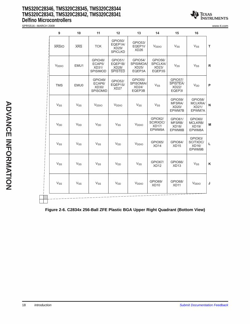
Figure 2-5. C2834x 256-Ball ZFE Plastic BGA Upper Left Quadrant (Bottom View)
Submit Documentation Feedback Introduction 17
AD
VAN
CE
INF
OR
MA
TIO
N VDDIO
9
TVSS
10
R
P
11 12
GPIO58/
MCLKRA/
XD21/
EPWM7A
13 14 15 16
GPIO64/
XD15
GPIO59/
MFSRA/
XD20/
EPWM7B
GPIO57/
/
XD22/
EQEP3I
SPISTEA
GPIO56/
SPICLKA/
XD23/
EQEP3S
NVSS VSSVDDIO VDDIO
MVSS
LVDD VDDIO
TCK
KVSS
J
GPIO63/
SCITXDC/
XD16/
EPWM9B
GPIO60/
MCLKRB/
XD19/
EPWM8A
VDD
VSS
VSS
GPIO68/
XD11
GPIO66/
XD13
GPIO61/
MFSRB/
XD18/
EPWM8B
VSS VSS
GPIO65/
XD14
GPIO69/
XD10
GPIO67/
XD12
GPIO62/
SCIRXDC/
XD17/
EPWM9A
VDDIO
VSS
VSS
VDDIO
GPIO53/
EQEP1I/
XD26
GPIO55/
SPISOMIA/
XD24/
EQEP3B
GPIO54/
SPISIMOA/
XD25/
EQEP3A
VDD VDD VDD VDDIO
GPIO50/
EQEP1A/
XD29/
SPICLKD
GPIO52/
EQEP1S/
XD27
GPIO51/
EQEP1B/
XD28/
SPISTED
VSS VSS VSS
GPIO49/
ECAP6/
XD30/
SPISOMID
GPIO48/
ECAP5/
XD31/
SPISIMOD
VSS VSS VDD VSS
XRS
EMU0
EMU1
VSS VSS VSS VDD
VSS
TMS
VDDIO
XRSIO
TMS320C28346, TMS320C28345, TMS320C28344TMS320C28343, TMS320C28342, TMS320C28341Delfino MicrocontrollersSPRS516–MARCH 2009 www.ti.com
Figure 2-6. C2834x 256-Ball ZFE Plastic BGA Upper Right Quadrant (Bottom View)
18 Introduction Submit Documentation Feedback

AD
VAN
CE
INF
OR
MA
TIO
N
VSSK
1
H
2
X1
G
VDD18
F
3 4 5 6 7 8
GPIO81/
XA9
GPIO82/
XA10
E
GPIO84/
XA12
GPIO85/
XA13
D
GPIO39/
XA16
C
VDDIO
GPIO31/
CANTXA/
XA17
B VSS
GPIO30/
CANRXA/
XA18
A
VDD
GPIO46/
XA6
GPIO47/
XA7
VDDIO
VDD VSS VSS VSS
GPIO80/
XA8
VSS
VDD
VSS VSS VSS
GPIO83/
XA11
VDDIO
VDD
VSS VSS VSS
GPIO86/
XA14
VDDIO VSS VDD VDD
VDD
GPIO87/
XA15
VSS VSS VDDIO VDDIO VSS
VSS
VSS VSS
GPIO6/
EPWM4A/
EPWMSYNCI/
EPWMSYNCO
GPIO3/
EPWM2B/
ECAP5/
MCLKRB
GPIO12/
/
CANTXB/
MDXB
TZ1
GPIO9/
EPWM5B/
SCITXDB/
ECAP3
VSS
GPIO0/
EPWM1A
GPIO2/
EPWM2A
GPIO5/
EPWM3B/
MFSRA/
ECAP1
GPIO8/
EPWM5A/
CANTXB/
ADCSOCAO
GPIO11/
EPWM6B/
SCIRXDB/
ECAP4
VSS VSS
GPIO29/
SCITXDA/
XA19
GPIO1/
EPWM1B/
ECAP6/
MFSRB
GPIO4/
EPWM3A
GPIO7/
EPWM4B/
MCLKRA/
ECAP2
GPIO10/
EPWM6A/
CANRXB/
ADCSOCBO
TMS320C28346, TMS320C28345, TMS320C28344TMS320C28343, TMS320C28342, TMS320C28341
Delfino Microcontrollerswww.ti.com SPRS516–MARCH 2009
Figure 2-7. C2834x 256-Ball ZFE Plastic BGA Lower Left Quadrant (Bottom View)
Submit Documentation Feedback Introduction 19

AD
VAN
CE
INF
OR
MA
TIO
N
9
HVSS
10
G
F
11 12 13 14 15 16
E
C
B
A
D
VSS
VSS VSS VDD
VSS
VSS
VSS VDD VSS
VSS
VSS
VSS VDD VDDIO
VDD VDD VDD VSS VDDIO
VDD18
VSS VDDIO VDDIO VSS VSS
VDDVSS
VDDIO
VSS VSSVDDIO
VSS VSS
GPIO36/
SCIRXDA/
XZCS0
VSS
GPIO38/
XWE0
VSS
XRD
GPIO77/
XD2
GPIO74/
XD5
GPIO71/
XD8
GPIO34/
ECAP1/
XREADY
GPIO78/
XD1
GPIO75/
XD4
GPIO72/
XD7
GPIO28/
SCIRXDA/
XZCS6
GPIO37/
ECAP2/
XZCS7
GPIO41/
XA1
GPIO43/
XA3
GPIO35/
SCITXDA/
XR/W
X2 XCLKIN
GPIO40/
XA0
GPIO42/
XA2
GPIO44/
XA4
GPIO45/
XA5
XCLKOUT
GPIO79/
XD0
GPIO76/
XD3
GPIO73/
XD6
GPIO70/
XD9
XWE1
VSS
TMS320C28346, TMS320C28345, TMS320C28344TMS320C28343, TMS320C28342, TMS320C28341Delfino MicrocontrollersSPRS516–MARCH 2009 www.ti.com
Figure 2-8. C2834x 256-Ball ZFE Plastic BGA Lower Right Quadrant (Bottom View)
20 Introduction Submit Documentation Feedback

AD
VAN
CE
INF
OR
MA
TIO
N
2.2 Signal Descriptions
TMS320C28346, TMS320C28345, TMS320C28344TMS320C28343, TMS320C28342, TMS320C28341
Delfino Microcontrollerswww.ti.com SPRS516–MARCH 2009
Table 2-2 describes the signals. The GPIO function (shown in Italics) is the default at reset. The peripheralsignals that are listed under them are alternate functions. Some peripheral functions may not be availablein all devices. See for details. Inputs are not 5-V tolerant. All XINTF pins have a drive strength of 4 mA(typical). All GPIO pins are I/O/Z, 4-mA drive typical and have an internal pullup, which can be selectivelyenabled/disabled on a per-pin basis. This feature only applies to the GPIO pins. The pullups onGPIO0-GPIO11 pins are not enabled at reset. The pullups on GPIO12-GPIO34 are enabled upon reset.
Table 2-2. Signal DescriptionsZHH ZFENAME DESCRIPTIONBALL # BALL #
JTAGM7 R8 JTAG test reset with internal pulldown. TRST, when driven high, gives the scan system control of
the operations of the device. If this signal is not connected or driven low, the device operates in itsfunctional mode, and the test reset signals are ignored.NOTE: TRST is an active high test pin and must be maintained low at all times during normalTRST device operation. An external pulldown resistor is recommended on this pin. The value of thisresistor should be based on drive strength of the debugger pods applicable to the design. A 2.2-kΩresistor generally offers adequate protection. Since this is application-specific, it is recommendedthat each target board be validated for proper operation of the debugger and the application. (I, ↓)
P9 T11 JTAG test clock. An external pullup resistor is required on this pin. A 2.2-kΩ resistor generally offersTCK adequate protection.(I)M8 P9 JTAG test-mode select (TMS) with internal pullup. This serial control input is clocked into the TAPTMS controller on the rising edge of TCK. (I, ↑)L6 T8 JTAG test data input (TDI) with internal pullup. TDI is clocked into the selected register (instructionTDI or data) on a rising edge of TCK. (I, ↑)N7 P8 JTAG scan out, test data output (TDO). The contents of the selected register (instruction or data)TDO are shifted out of TDO on the falling edge of TCK.N9 P10 Emulator pin 0. When TRST is driven high, this pin is used as an interrupt to or from the emulator
system and is defined as input/output through the JTAG scan. This pin is also used to put thedevice into boundary-scan mode. With the EMU0 pin at a logic-high state and the EMU1 pin at alogic-low state, a rising edge on the TRST pin would latch the device into boundary-scan mode.EMU0 NOTE: An external pullup resistor is recommended on this pin. The value of this resistor should bebased on the drive strength of the debugger pods applicable to the design. A 2.2-kΩ to 4.7-kΩresistor is generally adequate. Since this is application-specific, it is recommended that each targetboard be validated for proper operation of the debugger and the application.
L9 R10 Emulator pin 1. When TRST is driven high, this pin is used as an interrupt to or from the emulatorsystem and is defined as input/output through the JTAG scan. This pin is also used to put thedevice into boundary-scan mode. With the EMU0 pin at a logic-high state and the EMU1 pin at alogic-low state, a rising edge on the TRST pin would latch the device into boundary-scan mode.EMU1 NOTE: An external pullup resistor is recommended on this pin. The value of this resistor should bebased on the drive strength of the debugger pods applicable to the design. A 2.2-kΩ to 4.7-kΩresistor is generally adequate. Since this is application-specific, it is recommended that each targetboard be validated for proper operation of the debugger and the application.
ClockB14 D16 Output clock derived from SYSCLKOUT. XCLKOUT is either the same frequency, one-half the
frequency, one-fourth the frequency, or one-eighth the frequency of SYSCLKOUT. This is controlledby bit 19 (BY4CLKMODE), bits 18:16 (XTIMCLK), and bit 2 (CLKMODE) in the XINTCNF2 register.XCLKOUT At reset, XCLKOUT = SYSCLKOUT/8. The XCLKOUT signal can be turned off by settingXINTCNF2[CLKOFF] to 1. Unlike other GPIO pins, the XCLKOUT pin is not placed inhigh-impedance state during a reset.
D9 A12 External Oscillator Input. This pin is to feed a clock from an external 3.3-V oscillator. In this case,XCLKIN the X1 pin must be tied to VSSK. If a crystal/resonator is used (or if an external 1.8-V oscillator is
used to feed clock to X1 pin), this pin must be tied to VSS. (I)C8 A7 Internal/External Oscillator Input. To use the internal oscillator, a quartz crystal may be connected
across X1 and X2. The X1 pin is referenced to the 1.8-V core digital power supply. A 1.8-V externalX1 oscillator may be connected to the X1 pin. In this case, the XCLKIN pin must be connected to VSS.If a 3.3-V external oscillator is used with the XCLKIN pin, X1 must be tied to VSSK. (I)
A8 A9 Internal Oscillator Output. A quartz crystal may be connected across X1 and X2. If X2 is not used itX2 must be left unconnected. (O)
Submit Documentation Feedback Introduction 21

AD
VAN
CE
INF
OR
MA
TIO
N
TMS320C28346, TMS320C28345, TMS320C28344TMS320C28343, TMS320C28342, TMS320C28341Delfino MicrocontrollersSPRS516–MARCH 2009 www.ti.com
Table 2-2. Signal Descriptions (continued)ZHH ZFENAME DESCRIPTIONBALL # BALL #
ResetDevice Reset (in) and Watchdog Reset (out).Device reset. XRS causes the device to terminate execution. The PC will point to the addresscontained at the location 0x3FFFC0. When XRS is brought to a high level, execution begins at thelocation pointed to by the PC. This pin is driven low by the MCU when a watchdog reset occurs.XRS P8 T10 During watchdog reset, the XRS pin is driven low for the watchdog reset duration of 512 OSCCLKcycles. (I/OD, ↑)The output buffer of this pin is an open-drain with an internal pullup. It is recommended that this pinbe driven by an open-drain device.XRS I/O Control (I) - This pin must be connected to the XRS pin on the target board. When XRS is
XRSIO N8 T9 low (reset), the level detected on this pin puts all output buffers on the device.in high-impedancemode.
External ADC Interface SignalsEXTSOC1A N1 M2 External ADC SOC Group 1 A Output. Trigger for external ADC, this signal is logical OR of
ePWM1/2/3 SOCA internal signals (O)EXTSOC1B M3 M3 External ADC SOC Group 1 B Output. Trigger for external ADC, this signal is logical OR of
ePWM1/2/3 SOCB internal signals (O)EXTSOC2A M2 N1 External ADC SOC Group 2 A Output. Trigger for external ADC, this signal is logical OR of
ePWM4/5/6 SOCA internal signals (O)EXTSOC2B P1 N2 External ADC SOC Group 2 B Output. Trigger for external ADC, this signal is logical OR of
ePWM4/5/6 SOCB internal signals (O)EXTSOC3A N2 N3 External ADC SOC Group 3 A Output. Trigger for external ADC, this signal is logical OR of
ePWM7/8/9 SOCA internal signals (O)EXTSOC3B P2 P2 External ADC SOC Group3 B Output. Trigger for external ADC, this signal is logical OR of
ePWM7/8/9 SOCB internal signals (O)EXTADCCLK N3 R3 External ADC Clock Signal. Clock for external ADC support, derived from SYSCLK (O)
GPIO and Peripheral SignalsGPIO0 General purpose input/output 0 (I/O/Z)EPWM1A Enhanced PWM1 Output A and HRPWM channel (O)B1 D2- -- -GPIO1 General purpose input/output 1 (I/O/Z)EPWM1B Enhanced PWM1 Output B (O)C1 E1ECAP6 Enhanced Capture 6 input/output (I/O)MFSRB McBSP-B receive frame synch (I/O)GPIO2 General purpose input/output 2 (I/O/Z)EPWM2A Enhanced PWM2 Output A and HRPWM channel (O)F5 E2- -- -GPIO3 General purpose input/output 3 (I/O/Z)EPWM2B Enhanced PWM2 Output B (O)E4 E3ECAP5 Enhanced Capture 5 input/output (I/O)MCLKRB McBSP-B receive clock (I/O)GPIO4 General purpose input/output 4 (I/O/Z)EPWM3A Enhanced PWM3 output A and HRPWM channel (O)E2 F1- -- -GPIO5 General purpose input/output 5 (I/O/Z)EPWM3B Enhanced PWM3 output B (O)E3 F2MFSRA McBSP-A receive frame synch (I/O)ECAP1 Enhanced Capture input/output 1 (I/O)GPIO6 General purpose input/output 6 (I/O/Z)EPWM4A Enhanced PWM4 output A and HRPWM channel (O)F3 F3EPWMSYNCI External ePWM sync pulse input (I)EPWMSYNCO External ePWM sync pulse output (O)GPIO7 General purpose input/output 7 (I/O/Z)EPWM4B Enhanced PWM4 output B (O)F2 G1MCLKRA McBSP-A receive clock (I/O)ECAP2 Enhanced capture input/output 2 (I/O)
Introduction22 Submit Documentation Feedback

AD
VAN
CE
INF
OR
MA
TIO
N
TMS320C28346, TMS320C28345, TMS320C28344TMS320C28343, TMS320C28342, TMS320C28341
Delfino Microcontrollerswww.ti.com SPRS516–MARCH 2009
Table 2-2. Signal Descriptions (continued)ZHH ZFENAME DESCRIPTIONBALL # BALL #
GPIO8 General Purpose Input/Output 8 (I/O/Z)EPWM5A Enhanced PWM5 output A and HRPWM channel (O)G4 G2CANTXB Enhanced CAN-B transmit (O)ADCSOCAO ADC start-of-conversion A (O)GPIO9 General purpose input/output 9 (I/O/Z)EPWM5B Enhanced PWM5 output B (O)G2 G3SCITXDB SCI-B transmit data(O)ECAP3 Enhanced capture input/output 3 (I/O)GPIO10 General purpose input/output 10 (I/O/Z)EPWM6A Enhanced PWM6 output A and HRPWM channel (O)G3 H1CANRXB Enhanced CAN-B receive (I)ADCSOCBO ADC start-of-conversion B (O)GPIO11 General purpose input/output 11 (I/O/Z)EPWM6B Enhanced PWM6 output B (O)H3 H2SCIRXDB SCI-B receive data (I)ECAP4 Enhanced CAP Input/Output 4 (I/O)GPIO12 General purpose input/output 12 (I/O/Z)TZ1 Trip Zone input 1 (I)H2 H3CANTXB Enhanced CAN-B transmit (O)MDXB McBSP-B transmit serial data (O)GPIO13 General purpose input/output 13 (I/O/Z)TZ2 Trip Zone input 2 (I)H4 J2CANRXB Enhanced CAN-B receive (I)MDRB McBSP-B receive serial data (I)GPIO14 General purpose input/output 14 (I/O/Z)
Trip Zone input 3/External Hold Request. XHOLD, when active (low), requests the external interface(XINTF) to release the external bus and place all buses and strobes into a high-impedance state. Toprevent this from happening when TZ3 signal goes active, disable this function by writing
TZ3/XHOLD XINTCNF2[HOLD] = 1. If this is not done, the XINTF bus will go into high impedance anytime TZ3H5 J3 goes low. On the ePWM side, TZn signals are ignored by default, unless they are enabled by thecode. The XINTF will release the bus when any current access is complete and there are nopending accesses on the XINTF. (I)
SCITXDB SCI-B Transmit (I)MCLKXB McBSP-B transmit clock (I/O)GPIO15 General purpose input/output 15 (I/O/Z)
Trip Zone input 4/External Hold Acknowledge. The pin function for this option is based on thedirection chosen in the GPADIR register. If the pin is configured as an input, then TZ4 function ischosen. If the pin is configured as an output, then XHOLDA function is chosen. XHOLDA is drivenTZ4/XHOLDA K2 K2 active (low) when the XINTF has granted an XHOLD request. All XINTF buses and strobe signalswill be in a high-impedance state. XHOLDA is released when the XHOLD signal is released.External devices should only drive the external bus when XHOLDA is active (low). (I/0)
SCIRXDB SCI-B receive (I)MFSXB McBSP-B transmit frame synch (I/O)GPIO16 General purpose input/output 16 (I/O/Z)SPISIMOA SPI slave in, master out (I/O)K4 L1CANTXB Enhanced CAN-B transmit (O)TZ5 Trip Zone input 5 (I)GPIO17 General purpose input/output 17 (I/O/Z)SPISOMIA SPI-A slave out, master in (I/O)J5 L2CANRXB Enhanced CAN-B receive (I)TZ6 Trip zone input 6 (I)GPIO18 General purpose input/output 18 (I/O/Z)SPICLKA SPI-A clock input/output (I/O)L1 M1SCITXDB SCI-B transmit (O)CANRXA Enhanced CAN-A receive (I)GPIO19 General purpose input/output 19 (I/O/Z)SPISTEA SPI-A slave transmit enable input/output (I/O)P3 T4SCIRXDB SCI-B receive (I)CANTXA Enhanced CAN-A transmit (O)
Submit Documentation Feedback Introduction 23

AD
VAN
CE
INF
OR
MA
TIO
N
TMS320C28346, TMS320C28345, TMS320C28344TMS320C28343, TMS320C28342, TMS320C28341Delfino MicrocontrollersSPRS516–MARCH 2009 www.ti.com
Table 2-2. Signal Descriptions (continued)ZHH ZFENAME DESCRIPTIONBALL # BALL #
GPIO20 General purpose input/output 20 (I/O/Z)EQEP1A Enhanced QEP1 input A (I)L4 R4MDXA McBSP-A transmit serial data (O)CANTXB Enhanced CAN-B transmit (O)GPIO21 General purpose input/output 21 (I/O/Z)EQEP1B Enhanced QEP1 input B (I)M4 T5MDRA McBSP-A receive serial data (I)CANRXB Enhanced CAN-B receive (I)GPIO22 General purpose input/output 22 (I/O/Z)EQEP1S Enhanced QEP1 strobe (I/O)N4 R5MCLKXA McBSP-A transmit clock (I/O)SCITXDB SCI-B transmit (O)GPIO23 General purpose input/output 23 (I/O/Z)EQEP1I Enhanced QEP1 index (I/O)P4 P5MFSXA McBSP-A transmit frame synch (I/O)SCIRXDB SCI-B receive (I)GPIO24 General purpose input/output 24 (I/O/Z)ECAP1 Enhanced capture 1 (I/O)P5 T6EQEP2A Enhanced QEP2 input A (I)MDXB McBSP-B transmit serial data (O)GPIO25 General purpose input/output 25 (I/O/Z)ECAP2 Enhanced capture 2 (I/O)M5 R6EQEP2B Enhanced QEP2 input B (I)MDRB McBSP-B receive serial data (I)GPIO26 General purpose input/output 26 (I/O/Z)ECAP3 Enhanced capture 3 (I/O)K6 P6EQEP2I Enhanced QEP2 index (I/O)MCLKXB McBSP-B transmit clock (I/O)GPIO27 General purpose input/output 27 (I/O/Z)ECAP4 Enhanced capture 4 (I/O)M6 T7EQEP2S Enhanced QEP2 strobe (I/O)MFSXB McBSP-B transmit frame synch (I/O)GPIO28 General purpose input/output 28 (I/O/Z)SCIRXDA A12 B13 SCI receive data (I)XZCS6 External Interface zone 6 chip select (O)GPIO29 General purpose input/output 29. (I/O/Z)SCITXDA C3 D1 SCI transmit data (O)XA19 External Interface Address Line 19 (O)GPIO30 General purpose input/output 30 (I/O/Z)CANRXA C2 C2 Enhanced CAN-A receive (I)XA18 External Interface Address Line 18 (O)GPIO31 General purpose input/output 31 (I/O/Z)CANTXA B2 B3 Enhanced CAN-A transmit (O)XA17 External Interface Address Line 17 (O)GPIO32 General purpose input/output 32 (I/O/Z)SDAA I2C data open-drain bidirectional port (I/OD)P6 R7EPWMSYNCI Enhanced PWM external sync pulse input (I)ADCSOCAO ADC start-of-conversion A (O)GPIO33 General-Purpose Input/Output 33 (I/O/Z)SCLA I2C clock open-drain bidirectional port (I/OD)N6 P7EPWMSYNCO Enhanced PWM external synch pulse output (O)ADCSOCBO ADC start-of-conversion B (O)GPIO34 General-Purpose Input/Output 34 (I/O/Z)ECAP1 A13 B14 Enhanced Capture input/output 1 (I/O)XREADY External Interface Ready signalGPIO35 General-Purpose Input/Output 35 (I/O/Z)SCITXDA B13 C15 SCI-A transmit data (O)XR/W External Interface read, not write strobe
Introduction24 Submit Documentation Feedback

AD
VAN
CE
INF
OR
MA
TIO
N
TMS320C28346, TMS320C28345, TMS320C28344TMS320C28343, TMS320C28342, TMS320C28341
Delfino Microcontrollerswww.ti.com SPRS516–MARCH 2009
Table 2-2. Signal Descriptions (continued)ZHH ZFENAME DESCRIPTIONBALL # BALL #
GPIO36 General-Purpose Input/Output 36 (I/O/Z)SCIRXDA B12 A13 SCI-A receive data (I)XZCS0 External Interface zone 0 chip select (O)GPIO37 General-Purpose Input/Output 37 (I/O/Z)ECAP2 D11 B12 Enhanced Capture input/output 2 (I/O)XZCS7 External Interface zone 7 chip select (O)GPIO38 General-Purpose Input/Output 38 (I/O/Z)- C12 E15 -XWE0 External Interface Write Enable 0 (O)GPIO39 General-Purpose Input/Output 39 (I/O/Z)- A2 B4 -XA16 External Interface Address Line 16 (O)GPIO40 General-Purpose Input/Output 40 (I/O/Z)- E10 C12 -XA0 External Interface Address Line 0GPIO41 General-Purpose Input/Output 41 (I/O/Z)- D10 B11 -XA1 External Interface Address Line 1 (O)GPIO42 General-Purpose Input/Output 42 (I/O/Z)- B10 C11 -XA2 External Interface Address Line 2 (O)GPIO43 General-Purpose Input/Output 43 (I/O/Z)- A10 B10 -XA3 External Interface Address Line 3 (O)GPIO44 General-Purpose Input/Output 44 (I/O/Z)- A9 C10 -XA4 External Interface Address Line 4 (O)GPIO45 General-Purpose Input/Output 45 (I/O/Z)- B9 C9 -XA5 External Interface Address Line 5 (O)GPIO46 General-Purpose Input/Output 46 (I/O/Z)- E7 B8 -XA6 External Interface Address Line 6 (O)GPIO47 General-Purpose Input/Output 47 (I/O/Z)- D6 C8 -XA7 External Interface Address Line 7 (O)GPIO48 General-Purpose Input/Output 48 (I/O/Z)ECAP5 Enhanced Capture input/output 5 (I/O)M10 R11XD31 External Interface Data Line 31 (O)SPISIMOD SPI-D slave in, master out (I/O)GPIO49 General-Purpose Input/Output 49 (I/O/Z)ECAP6 Enhanced Capture input/output 6 (I/O)P10 P11XD30 External Interface Data Line 30 (O)SPISOMID SPI-D slave out, master in (I/O)GPIO50 General-Purpose Input/Output 50 (I/O/Z)EQEP1A Enhanced QEP 1input A (I)N10 T12XD29 External Interface Data Line 29 (O)SPICLKD SPI-D Clock input/output (I/O)GPIO51 General-Purpose Input/Output 51 (I/O/Z)EQEP1B Enhanced QEP 1input B (I)N11 R12XD28 External Interface Data Line 28 (O)SPISTED SPI-D slave transmit enable input/output (I/O)GPIO52 General-Purpose Input/Output 52 (I/O/Z)EQEP1S M11 P12 Enhanced QEP 1Strobe (I/O)XD27 External Interface Data Line 27 (O)GPIO53 General-Purpose Input/Output 53 (I/O/Z)EQEP1I L11 T13 Enhanced CAP1 lndex (I/O)XD26 External Interface Data Line 26 (O)
Submit Documentation Feedback Introduction 25

AD
VAN
CE
INF
OR
MA
TIO
N
TMS320C28346, TMS320C28345, TMS320C28344TMS320C28343, TMS320C28342, TMS320C28341Delfino MicrocontrollersSPRS516–MARCH 2009 www.ti.com
Table 2-2. Signal Descriptions (continued)ZHH ZFENAME DESCRIPTIONBALL # BALL #
GPIO54 General-Purpose Input/Output 54 (I/O/Z)SPISIMOA SPI-A slave in, master out (I/O)P12 R13XD25 External Interface Data Line 25 (O)EQEP3A Enhanced QEP3 input A (I)GPIO55 General-Purpose Input/Output 55 (I/O/Z)SPISOMIA SPI-A slave out, master in (I/O)N12 P13XD24 External Interface Data Line 24 (O)EQEP3B Enhanced QEP3 input B (I)GPIO56 General-Purpose Input/Output 56 (I/O/Z)SPICLKA SPI-A clock (I/O)P13 R14XD23 External Interface Data Line 23 (O)EQEP3S Enhanced QEP3 strobe (I/O)GPIO57 General-Purpose Input/Output 57 (I/O/Z)SPISTEA SPI-A slave transmit enable (I/O)N13 P15XD22 External Interface Data Line 22 (O)EQEP3I Enhanced QEP3 index (I/O)GPIO58 General-Purpose Input/Output 58 (I/O/Z)MCLKRA McBSP-A receive clock (I/O)P14 N16XD21 External Interface Data Line 21 (O)EPWM7A Enhanced PWM 7 output A and HRPWM channel (O)GPIO59 General-Purpose Input/Output 59 (I/O/Z)MFSRA McBSP-A receive frame synch (I/O)M13 N15XD20 External Interface Data Line 20 (O)EPWM7B Enhanced PWM 7 output B (O)GPIO60 General-Purpose Input/Output 60 (I/O/Z)MCLKRB McBSP-B receive clock (I/O)M14 M16XD19 External Interface Data Line 19 (O)EPWM8A Enhanced PWM 8 output A and HRPWM channel (O)GPIO61 General-Purpose Input/Output 61 (I/O/Z)MFSRB McBSP-B receive frame synch (I/O)L12 M15XD18 External Interface Data Line 18 (O)EPWM8B Enhanced PWM8 output B (O)GPIO62 General-Purpose Input/Output 62 (I/O/Z)SCIRXDC SCI-C receive data (I)L13 M14XD17 External Interface Data Line 17 (O)EPWM9A Enhanced PWM9 output A and HRPWM channel (O)GPIO63 General-Purpose Input/Output 63 (I/O/Z)SCITXDC SCI-C transmit data (O)K13 L16XD16 External Interface Data Line 16 (O)EPWM9B Enhanced PWM9 output B (O)GPIO64 General-Purpose Input/Output 64 (I/O/Z)- K12 L15 -XD15 External Interface Data Line 15 (O)GPIO65 General-Purpose Input/Output 65 (I/O/Z)- K14 L14 -XD14 External Interface Data Line 14 (O)GPIO66 General-Purpose Input/Output 66 (I/O/Z)- J11 K15 -XD13 External Interface Data Line 13 (O)GPIO67 General-Purpose Input/Output 67 (I/O/Z)- J12 K14 -XD12 External Interface Data Line 12 (O)GPIO68 General-Purpose Input/Output 68 (I/O/Z)- J13 J15 -XD11 External Interface Data Line 11 (O)GPIO69 General-Purpose Input/Output 69 (I/O/Z)- H13 J14 -XD10 External Interface Data Line 10 (O)
Introduction26 Submit Documentation Feedback

AD
VAN
CE
INF
OR
MA
TIO
N
TMS320C28346, TMS320C28345, TMS320C28344TMS320C28343, TMS320C28342, TMS320C28341
Delfino Microcontrollerswww.ti.com SPRS516–MARCH 2009
Table 2-2. Signal Descriptions (continued)ZHH ZFENAME DESCRIPTIONBALL # BALL #
GPIO70 General-Purpose Input/Output 70 (I/O/Z)- H12 H16 -XD9 External Interface Data Line 9 (O)GPIO71 General-Purpose Input/Output 71 (I/O/Z)- G12 H15 -XD8 External Interface Data Line 8 (O)GPIO72 General-Purpose Input/Output 72 (I/O/Z)- G13 H14 -XD7 External Interface Data Line 7 (O)GPIO73 General-Purpose Input/Output 73 (I/O/Z)- F14 G16 -XD6 External Interface Data Line 6 (O)GPIO74 General-Purpose Input/Output 74 (I/O/Z)- F13 G15 -XD5 External Interface Data Line 5 (O)GPIO75 General-Purpose Input/Output 75 (I/O/Z)- F12 G14 -XD4 External Interface Data Line 4 (O)GPIO76 General-Purpose Input/Output 76 (I/O/Z)- E13 F16 -XD3 External Interface Data Line 3 (O)GPIO77 General-Purpose Input/Output 77 (I/O/Z)- E11 F15 -XD2 External Interface Data Line 2 (O)GPIO78 General-Purpose Input/Output 78 (I/O/Z)- F10 F14 -XD1 External Interface Data Line 1 (O)GPIO79 General-Purpose Input/Output 79 (I/O/Z)- C14 E16 -XD0 External Interface Data Line 0 (O)GPIO80 General-Purpose Input/Output 80 (I/O/Z)- E6 B7 -XA8 External Interface Address Line 8 (O)GPIO81 General-Purpose Input/Output 81 (I/O/Z)- C5 C7 -XA9 External Interface Address Line 9 (O)GPIO82 General-Purpose Input/Output 82 (I/O/Z)- A5 B6 -XA10 External Interface Address Line 10 (O)GPIO83 General-Purpose Input/Output 83 (I/O/Z)- B5 C6 -XA11 External Interface Address Line 11 (O)GPIO84 General-Purpose Input/Output 84 (I/O/Z)- D5 A5 -XA12 External Interface Address Line 12 (O)GPIO85 General-Purpose Input/Output 85 (I/O/Z)- D4 B5 -XA13 External Interface Address Line 13 (O)GPIO86 General-Purpose Input/Output 86 (I/O/Z)- A3 C5 -XA14 External Interface Address Line 14 (O)GPIO87 General-Purpose Input/Output 87 (I/O/Z)- B3 A4 -XA15 External Interface Address Line 15 (O)XRD A14 D15 External Interface Read Enable (O)XWE1 C13 E14 External Memory Interface Write Enable for Upper 16-bits (O)
Submit Documentation Feedback Introduction 27

AD
VAN
CE
INF
OR
MA
TIO
N
TMS320C28346, TMS320C28345, TMS320C28344TMS320C28343, TMS320C28342, TMS320C28341Delfino MicrocontrollersSPRS516–MARCH 2009 www.ti.com
Table 2-2. Signal Descriptions (continued)ZHH ZFENAME DESCRIPTIONBALL # BALL #
CPU and I/O Power PinsVDD18 E8 A6
Oscillator and PLL Power Pin (1.8 V)VDD18 C7 A11VSSK B8 A8 Oscillator Kelvin Reference Ground. This pin should not be connected to Vss. See Figure 3-10
through Figure 3-12 for proper application board connections.VDD D1 C1VDD E1 C16VDD G1 E6VDD K3 E7VDD M1 E8VDD N5 E9VDD P7 E10VDD J3 E11VDD J4 F5VDD K9 F12VDD L10 G5VDD N14 G12VDD K11 H5VDD H11 H12VDD H14 J5
CPU and logic digital power pins (1.1 V/1.2 V)VDD G10 J12VDD E12 K3VDD D12 K5VDD C11 K12VDD C10 L3VDD B7 L5VDD C6 L12VDD E5 M6VDD C4 M7VDD M8VDD M9VDD M10VDD M11VDD P1VDD P16VDDIO D3 A3VDDIO F1 A14VDDIO J1 B9VDDIO L2 D5VDDIO K5 D6 Digital I/O power pins (3.3 V)VDDIO K7 D8VDDIO K8 D11VDDIO P11 D12VDDIO L14 E4
Introduction28 Submit Documentation Feedback

AD
VAN
CE
INF
OR
MA
TIO
N
TMS320C28346, TMS320C28345, TMS320C28344TMS320C28343, TMS320C28342, TMS320C28341
Delfino Microcontrollerswww.ti.com SPRS516–MARCH 2009
Table 2-2. Signal Descriptions (continued)ZHH ZFENAME DESCRIPTIONBALL # BALL #
VDDIO J14 E13VDDIO F11 F4VDDIO D14 F13VDDIO A11 J1VDDIO C9 J4VDDIO D7 J13VDDIO B6 J16VDDIO B4 L4VDDIO L13VDDIO M4 Digital I/O power pinsVDDIO M13VDDIO N5VDDIO N6VDDIO N8VDDIO N11VDDIO N12VDDIO R9VDDIO T3VDDIO T14VSS D2 A1VSS F4 A2VSS G5 A10VSS H1 A15VSS J2 A16VSS K1 B1VSS L3 B2VSS L5 B15VSS L7 B16VSS L8 C3VSS M9 C4VSS K10 C13VSS M12 C14VSS J10 D3 Digital ground pinsVSS H10 D4VSS G14 D7VSS G11 D9VSS E14 D10VSS D13 D13VSS B11 D14VSS E9 E5VSS D8 E12VSS A7 F6VSS A6 F7VSS A4 F8VSS F9VSS F10
Submit Documentation Feedback Introduction 29

AD
VAN
CE
INF
OR
MA
TIO
N
TMS320C28346, TMS320C28345, TMS320C28344TMS320C28343, TMS320C28342, TMS320C28341Delfino MicrocontrollersSPRS516–MARCH 2009 www.ti.com
Table 2-2. Signal Descriptions (continued)ZHH ZFENAME DESCRIPTIONBALL # BALL #
VSS F11VSS G4VSS G6VSS G7VSS G8VSS G9VSS G10VSS G11VSS G13VSS H4VSS H6VSS H7VSS H8VSS H9VSS H10VSS H11VSS H13VSS J6VSS J7VSS J8VSS J9VSS J10VSS J11
Digital ground pinsVSS K1VSS K4VSS K6VSS K7VSS K8VSS K9VSS K10VSS K11VSS K13VSS K16VSS L6VSS L7VSS L8VSS L9VSS L10VSS L11VSS M5VSS M12VSS N4VSS N7VSS N9VSS N10VSS N13
Introduction30 Submit Documentation Feedback

AD
VAN
CE
INF
OR
MA
TIO
N
TMS320C28346, TMS320C28345, TMS320C28344TMS320C28343, TMS320C28342, TMS320C28341
Delfino Microcontrollerswww.ti.com SPRS516–MARCH 2009
Table 2-2. Signal Descriptions (continued)ZHH ZFENAME DESCRIPTIONBALL # BALL #
VSS N14VSS P3VSS P4VSS P14VSS R1VSS R2
Digital ground pinsVSS R15VSS R16VSS T1VSS T2VSS T15VSS T16
Submit Documentation Feedback Introduction 31

AD
VAN
CE
INF
OR
MA
TIO
N
3 Functional Overview
L0 SARAM 4K x 16
(0-Wait)
L1 SARAM 42K x 16
(0-Wait)
L2 SARAM 4K x 16
(0-Wait)
L3 SARAM 4K x 16
(0-Wait)
L4 SARAM 4K x 16
(0-Wait)
L5 SARAM 4K x 16
(0-Wait)Boot ROM
8K x 16
DM
AB
us
XIN
TF
XWE0
XZCS6
XZCS7
XZCS0
XR/W
XREADY
XHOLD
XHOLDA
XD31:0
XA19:1
GPIO
MUX
Me
mo
ry B
us
Memory Bus
XCLKOUT
XRD
GPIO
MUX
88 GPIOs8 External Interrupts
88 GPIOs
ADC
SoC
EXTADCCLK
EXTSOC
CPU Timer 0
CPU Timer 1
CPU Timer 2
OSC,
PLL,
LPM,
WD
DMA
6 Ch
PIE
(Interrupts)
32-bit CPU
(300 MHz @ 1.2 V
200 MHz @ 1.1 V)
EMU1
EMU0
TRST
TDO
TMS
TDI
TCK
XRS
X2
X1
XCLKIN
FPU
DMA Bus
Memory Bus
FIFO
(16 Levels)
SCI-A/B/C
FIFO
(16 Levels)
SPI-A/D
FIFO
(16 Levels)
I2C
16-bit peripheral bus
SP
ISO
MIx
SP
ISIM
Ox
SP
ICL
Kx
SP
IST
Ex
SC
IRX
Dx
SC
ITX
Dx
SD
Ax
SC
Lx
McBSP-A/B
MR
Xx
MD
Xx
MC
LK
Xx
MC
LK
Rx
MF
SX
x
MF
SR
x
32-bit peripheral bus
(DMA accessible)
ePWM-1/../9
HRPWM-1/../9
eCAP-1/../6 eQEP-1/2/3
EP
WM
xA
EP
WM
xB
ES
YN
CI
ES
YN
CO
TZ
x
EC
AP
x
EQ
EP
xA
EQ
EP
xB
EQ
EP
xI
EQ
EP
xS
CAN-A/B
(32-mbox)
CA
NR
Xx
CA
NT
Xx
M0 SARAM 1K x 16
(0-Wait)
M1 SARAM 1K x 16
(0-Wait)M
em
ory
Bu
s
32-bit peripheral bus
GPIO MUX
88 GPIOs
XWE1
H0 SARAM 32K x 16
(1 Wait, Prefetch)
H1 SARAM 32K x 16
(1 Wait, Prefetch)
H2 SARAM 32K x 16
(1 Wait, Prefetch)
H3 SARAM 32K x 16
(1 Wait, Prefetch)
H4 SARAM 32K x 16
(1 Wait, Prefetch)
H5 SARAM 32K x 16
(1 Wait, Prefetch)
L6 SARAM 4K x 16
(1-Wait)
L7 SARAM 4K x 16
(1-Wait)
DM
AB
us
TMS320C28346, TMS320C28345, TMS320C28344TMS320C28343, TMS320C28342, TMS320C28341Delfino MicrocontrollersSPRS516–MARCH 2009 www.ti.com
Figure 3-1. Functional Block Diagram
Functional Overview32 Submit Documentation Feedback

AD
VAN
CE
INF
OR
MA
TIO
N
3.1 Memory Maps
TMS320C28346, TMS320C28345, TMS320C28344TMS320C28343, TMS320C28342, TMS320C28341
Delfino Microcontrollerswww.ti.com SPRS516–MARCH 2009
In Figure 3-2 through Figure 3-4, the following apply:• Memory blocks are not to scale.• Peripheral Frame 0, Peripheral Frame 1, Peripheral Frame 2, and Peripheral Frame 3 memory maps
are restricted to data memory only. A user program cannot access these memory maps in programspace.
• Protected means the order of "Write followed by Read" operations is preserved rather than the pipelineorder. See the TMS320x2834x Delfino System Control and Interrupts Reference Guide (literaturenumber SPRUFN1) for more details.
• Certain memory ranges are EALLOW protected against spurious writes after configuration.• If the eCAN module is not used in an application, the RAM available (LAM, MOTS, MOTO, and
mailbox RAM) can be used as general-purpose RAM. The CAN module clock should be enabled forthis.
Submit Documentation Feedback Functional Overview 33

AD
VAN
CE
INF
OR
MA
TIO
N
Block
Start Address
0x00 0000
M0 Vector - RAM (32 x 32)(Enable if VMAP = 0)
Data Space Prog Space
M0 SARAM (1K x 16)
M1 SARAM (1K x 16)
Peripheral Frame 0
0x00 0040
0x00 0400
0x00 0800
PIE Vector - RAM
(256 x 16)
(Enabled if
VMAP = 1,
ENPIE =1)
Reserved
Reserved
L0 SARAM (8K x 16, DMA Accessible)
Peripheral Frame 1
(Protected)Reserved
Peripheral Frame 2
(Protected)
L1 SARAM (8K x 16, DMA Accessible)
H0 SARAM
(32K x 16 Prefetch)
Reserved
Boot ROM (8K x 16)
BROM Vector - ROM (32 x 32)
(Enable if VMAP = 1, ENPIE = 0)
0x00 0D00
0x00 0E00
0x00 2000
0x00 6000
0x00 7000
0x00 8000
0x00 A000
0x30 0000
0x3F FFC0
Data Space Prog Space
Reserved
XINTF Zone 0 (4K x 16, )XZCS0
(Protected) DMA Accessible
Reserved
On-Chip Memory External Memory XINTF
Only one of these vector maps-M0 vector, PIE vector, BROM vector-should be enabled at a time.
LEGEND:
L2 SARAM (8K x 16, DMA Accessible)
L3 SARAM (8K x 16, DMA Accessible)
L4 SARAM (8K x 16, DMA Accessible)
L5 SARAM (8K x 16, DMA Accessible)
0x00 C000
0x00 E000
0x01 0000
0x01 2000
0x01 4000
Reserved
0x00 4000
0x00 50000x00 5000
Peripheral Frame 3
(Protected) DMA Accessible
0x30 8000
0x31 0000
0x32 8000
0x33 FFF8
0x33 FFFF
0x3F E000
Peripheral Frame 0
XINTF Zone 6 (1M x 16, ) (DMA Accessible)XZCS60x10 0000
0x20 0000
0x30 0000XINTF Zone 7 (1M x 16, )XZCS7 (DMA Accessible)
0x31 8000
0x33 0000
0x32 0000
H1 SARAM
(32K x 16 Prefetch)
H2 SARAM
(32K x 16 Prefetch)
H3 SARAM
(32K x 16 Prefetch)
H4 SARAM
(32K x 16 Prefetch)
H5 SARAM
(32K x 16 Prefetch)
128-Bit Password(A)
Reserved
L6 SARAM (8K x 16, DMA Accessible)
L7 SARAM (8K x 16, DMA Accessible)0x01 6000
0x01 8000
Reserved
TMS320C28346, TMS320C28345, TMS320C28344TMS320C28343, TMS320C28342, TMS320C28341Delfino MicrocontrollersSPRS516–MARCH 2009 www.ti.com
A. These locations support compatibility with legacy C28x designs only. See Section 3.2.9.
Figure 3-2. C28346/C28345 Memory Map
Functional Overview34 Submit Documentation Feedback

AD
VAN
CE
INF
OR
MA
TIO
N
Block
Start Address
0x00 0000M0 Vector - RAM (32 x 32)
(Enable if VMAP = 0)
Data Space Prog Space
M0 SARAM (1K x 16)
M1 SARAM (1K x 16)
Peripheral Frame 0
0x00 0040
0x00 0400
0x00 0800
PIE Vector - RAM
(256 x 16)
(Enabled if
VMAP = 1,
ENPIE =1)
Reserved
Reserved
L0 SARAM (8K x 16, )DMA Accessible
Peripheral Frame 1
(Protected)Reserved
Peripheral Frame 2
(Protected)
L1 SARAM (8K x 16, )DMA Accessible
Reserved
Boot ROM (8K x 16)
BROM Vector - ROM (32 x 32)
(Enable if VMAP = 1, ENPIE = 0)
0x00 0D00
0x00 0E00
0x00 2000
0x00 6000
0x00 7000
0x00 8000
0x00 A000
0x3F FFC0
Data Space Prog Space
Reserved
XINTF Zone 0 (4K x 16, )
(Protected) DMA Accessible
XZCS0
Reserved
On-Chip Memory External Memory XINTF
Only one of these vector maps-M0 vector, PIE vector, BROM vector-should be enabled at a time.
LEGEND:
L2 SARAM (8K x 16, )DMA Accessible
L3 SARAM (8K x 16, )DMA Accessible
L4 SARAM (8K x 16, DMA Accessible)
L5 SARAM (8K x 16, DMA Accessible)
0x00 C000
0x00 E000
0x01 0000
0x01 2000
0x01 4000
Reserved
0x00 4000
0x00 50000x00 5000
Peripheral Frame 3
(Protected) DMA Accessible
0x33 FFF8
0x33 FFFF
0x3F E000
Peripheral Frame 0
XINTF Zone 6 (1M x 16, ) (DMA Accessible)XZCS60x10 0000
0x20 0000
0x30 0000XINTF Zone 7 (1M x 16, )XZCS7 (DMA Accessible)
H0 SARAM
(32K x 16 Prefetch)
0x30 0000
0x30 8000
0x31 0000
H1 SARAM
(32K x 16 Prefetch)
128-Bit Password(A)
Reserved
L6 SARAM (8K x 16, DMA Accessible)
L7 SARAM (8K x 16, DMA Accessible)0x01 6000
0x01 8000
Reserved
TMS320C28346, TMS320C28345, TMS320C28344TMS320C28343, TMS320C28342, TMS320C28341
Delfino Microcontrollerswww.ti.com SPRS516–MARCH 2009
A. These locations support compatibility with legacy C28x designs only. See Section 3.2.9.
Figure 3-3. C28344/C28343 Memory Map
Submit Documentation Feedback Functional Overview 35

AD
VAN
CE
INF
OR
MA
TIO
N
Block
Start Address
0x00 0000M0 Vector - RAM (32 x 32)
(Enable if VMAP = 0)
Data Space Prog Space
M0 SARAM (1K x 16)
M1 SARAM (1K x 16)
Peripheral Frame 0
0x00 0040
0x00 0400
0x00 0800
PIE Vector - RAM
(256 x 16)
(Enabled if
VMAP = 1,
ENPIE =1)
Reserved
Reserved
L0 SARAM (8K x 16, )DMA Accessible
Peripheral Frame 1
(Protected)Reserved
Peripheral Frame 2
(Protected)
L1 SARAM (8K x 16, )DMA Accessible
Reserved
Boot ROM (8K x 16)
BROM Vector - ROM (32 x 32)
(Enable if VMAP = 1, ENPIE = 0)
0x00 0D00
0x00 0E00
0x00 2000
0x00 6000
0x00 7000
0x00 8000
0x00 A000
0x3F FFC0
Data Space Prog Space
Reserved
XINTF Zone 0 (4K x 16, )
(Protected)
XZCS0
DMA Accessible
Reserved
On-Chip Memory External Memory XINTF
Only one of these vector maps-M0 vector, PIE vector, BROM vector-should be enabled at a time.
LEGEND:
L2 SARAM (8K x 16, )DMA Accessible
L3 SARAM (8K x 16, )DMA Accessible
0x00 C000
0x00 E000
0x01 0000
Reserved
0x00 4000
0x00 50000x00 5000
Peripheral Frame 3
(Protected) DMA Accessible
0x33 FFF8
0x33 FFFF
0x3F E000
Peripheral Frame 0
XINTF Zone 6 (1M x 16, ) (DMA Accessible)XZCS6
0x10 0000
0x20 0000
0x30 0000
XINTF Zone 7 (1M x 16, )XZCS7 (DMA Accessible)
H0 SARAM
(32K x 16 Prefetch)
0x30 0000
0x30 8000
0x31 0000
H1 SARAM
(32K x 16 Prefetch)
128-Bit Password(A)
Reserved
Reserved
TMS320C28346, TMS320C28345, TMS320C28344TMS320C28343, TMS320C28342, TMS320C28341Delfino MicrocontrollersSPRS516–MARCH 2009 www.ti.com
A. These locations support compatibility with legacy C28x designs only. See Section 3.2.9.
Figure 3-4. C28342, C28341 Memory Map
Functional Overview36 Submit Documentation Feedback

AD
VAN
CE
INF
OR
MA
TIO
N
TMS320C28346, TMS320C28345, TMS320C28344TMS320C28343, TMS320C28342, TMS320C28341
Delfino Microcontrollerswww.ti.com SPRS516–MARCH 2009
Peripheral Frame 1, Peripheral Frame 2, and Peripheral Frame 3 are grouped together to enable theseblocks to be write/read peripheral block protected. The protected mode ensures that all accesses to theseblocks happen as written. Because of the C28x pipeline, a write immediately followed by a read, todifferent memory locations, will appear in reverse order on the memory bus of the CPU. This can causeproblems in certain peripheral applications where the user expected the write to occur first (as written).The C28x CPU supports a block protection mode where a region of memory can be protected so as tomake sure that operations occur as written (the penalty is extra cycles are added to align the operations).This mode is programmable and by default, it will protect the selected zones.
The wait-states for the various spaces in the memory map area are listed in Table 3-1.
Submit Documentation Feedback Functional Overview 37

AD
VAN
CE
INF
OR
MA
TIO
N
TMS320C28346, TMS320C28345, TMS320C28344TMS320C28343, TMS320C28342, TMS320C28341Delfino MicrocontrollersSPRS516–MARCH 2009 www.ti.com
Table 3-1. Wait-statesWAIT-STATES WAIT-STATESAREA COMMENTS(CPU) (DMA) (1)
M0 and M1 SARAMs 0-wait FixedPeripheral Frame 0 0-wait (writes) 0-wait (reads)
1-wait (reads)Peripheral Frame 3 0-wait (writes) 0-wait (writes) Assumes no conflicts between CPU and DMA.
2-wait (reads) 1-wait (reads)Peripheral Frame 1 0-wait (writes) Cycles can be extended by peripheral generated ready.
2-wait (reads) Consecutive writes to the CAN will experience a 1-cyclepipeline hit.
Peripheral Frame 2 0-wait (writes) Fixed. Cycles cannot be extended by the peripheral.2-wait (reads)
L0 SARAM 0-wait data and Assumes no CPU conflictsprogramL1 SARAM
L2 SARAML3 SARAML4 SARAM 1-wait Assumes no conflicts between CPU and DMAL5 SARAML6 SARAM 1-waitL7 SARAM
XINTF Programmable Programmed via the XTIMING registers or extendable viaexternal XREADY signal.
1-wait minimum 1-wait is minimum wait states allowed on external waveformsfor both reads and writes on XINTF.
0-wait minimum writes 0-wait data (write) 0-wait minimum for writes assumes write buffer enabled andwith write buffer 0-wait data (read) not full.
enabled Assumes no conflicts between CPU and DMA. When DMAand CPU attempt simultaneous conflict, 1-cycle delay isadded for arbitration.
H0 SARAM 1-wait A program-access prefetch mechanism is enabled on thesememories to improve instruction fetch performance for linearH1 SARAM code execution.
H2 SARAMH3 SARAMH4 SARAMH5 SARAMBoot-ROM 1-wait
(1) The DMA has a base of 4 cycles/word.
Functional Overview38 Submit Documentation Feedback

AD
VAN
CE
INF
OR
MA
TIO
N
3.2 Brief Descriptions
3.2.1 C28x CPU
3.2.2 Memory Bus (Harvard Bus Architecture)
3.2.3 Peripheral Bus
TMS320C28346, TMS320C28345, TMS320C28344TMS320C28343, TMS320C28342, TMS320C28341
Delfino Microcontrollerswww.ti.com SPRS516–MARCH 2009
The C2834x (C28x+FPU) family is a member of the TMS320C2000™ microcontroller (MCU) platform. TheC28x+FPU based controllers have the same 32-bit fixed-point architecture as TI's existing C28x MCUs,but also include a single-precision (32-bit) IEEE 754 floating-point unit (FPU). It is a very efficient C/C++engine, enabling users to develop their system control software in a high-level language. It also enablesmath algorithms to be developed using C/C++. The device is as efficient in DSP math tasks as it is insystem control tasks. This efficiency removes the need for a second processor in many systems. The 32 x32-bit MAC 64-bit processing capabilities enable the controller to handle higher numerical resolutionproblems efficiently. Add to this the fast interrupt response with automatic context save of critical registers,resulting in a device that is capable of servicing many asynchronous events with minimal latency. Thedevice has an 8-level-deep protected pipeline with pipelined memory accesses. This pipelining enables itto execute at high speeds without resorting to expensive high-speed memories. Specialbranch-look-ahead hardware minimizes the latency for conditional discontinuities. Special store conditionaloperations further improve performance.
As with many MCU type devices, multiple busses are used to move data between the memories andperipherals and the CPU. The C28x memory bus architecture contains a program read bus, data read busand data write bus. The program read bus consists of 22 address lines and 32 data lines. The data readand write busses consist of 32 address lines and 32 data lines each. The 32-bit-wide data busses enablesingle cycle 32-bit operations. The multiple bus architecture, commonly termed Harvard Bus, enables theC28x to fetch an instruction, read a data value and write a data value in a single cycle. All peripherals andmemories attached to the memory bus will prioritize memory accesses. Generally, the priority of memorybus accesses can be summarized as follows:
Highest: Data Writes (Simultaneous data and program writes cannot occur on the memorybus.)
Program Writes (Simultaneous data and program writes cannot occur on the memorybus.)
Data ReadsProgram (Simultaneous program reads and fetches cannot occur on the memoryReads bus.)
Lowest: Fetches (Simultaneous program reads and fetches cannot occur on the memorybus.)
To enable migration of peripherals between various Texas Instruments (TI) MCU family of devices, theC2834x devices adopt a peripheral bus standard for peripheral interconnect. The peripheral bus bridgemultiplexes the various busses that make up the processor Memory Bus into a single bus consisting of 16address lines and 16 or 32 data lines and associated control signals. Three versions of the peripheral busare supported. One version supports only 16-bit accesses (called peripheral frame 2). Another versionsupports both 16- and 32-bit accesses (called peripheral frame 1). The third version supports DMA accessand both 16- and 32-bit accesses (called peripheral frame 3).
Submit Documentation Feedback Functional Overview 39

AD
VAN
CE
INF
OR
MA
TIO
N
3.2.4 Real-Time JTAG and Analysis
3.2.5 External Interface (XINTF)
3.2.6 M0, M1 SARAMs
3.2.7 L0, L1, L2, L3, L4, L5, L6, L7, H0, H1, H2, H3, H4, H5 SARAMs
3.2.8 Boot ROM
TMS320C28346, TMS320C28345, TMS320C28344TMS320C28343, TMS320C28342, TMS320C28341Delfino MicrocontrollersSPRS516–MARCH 2009 www.ti.com
The C2834x devices implement the standard IEEE 1149.1 JTAG interface. Additionally, the devicessupport real-time mode of operation whereby the contents of memory, peripheral and register locationscan be modified while the processor is running and executing code and servicing interrupts. The user canalso single step through non-time critical code while enabling time-critical interrupts to be serviced withoutinterference. The device implements the real-time mode in hardware within the CPU. This is a featureunique to the C2834x device, requiring no software monitor. Additionally, special analysis hardware isprovided that allows setting of hardware breakpoint or data/address watch-points and generate varioususer-selectable break events when a match occurs.
This asynchronous interface consists of 20 address lines, 32 data lines, and three chip-select lines. Thechip-select lines are mapped to three external zones, Zones 0, 6, and 7. Each of the three zones can beprogrammed with a different number of wait states, strobe signal setup and hold timing and each zone canbe programmed for extending wait states externally or not. The programmable wait-state, chip-select andprogrammable strobe timing enables glueless interface to external memories and peripherals.
All C2834x devices contain these two blocks of single access memory, each 1K × 16 in size. The stackpointer points to the beginning of block M1 on reset. The M0 and M1 blocks, like all other memory blockson C28x devices, are mapped to both program and data space. Hence, the user can use M0 and M1 toexecute code or for data variables. The partitioning is performed within the linker. The C28x devicepresents a unified memory map to the programmer. This makes for easier programming in high-levellanguages.
The 2834x has up to 256K x 16 single-access RAM (SARAM) divided up into the following categories:
L0/1/2/3/4/5 SARAM Blocks Up to 48K x 16 of SARAM at all frequencies. Each block is8K x 16.
L6/L7 SARAM Blocks These 8K x 16 SARAM blocks are single-wait state at allfrequencies.
H0/1/2/3/4/5 SARAM Blocks H0-H5 are each 32K x 16 and 1-wait state at allfrequencies. A program-access prefetch buffer is used toimprove performance of linear code.
All SARAM blocks are mapped to both program and data space. L0-L7 are accessible by both the CPUand the DMA (1 wait state).
The Boot ROM is factory-programmed with boot-loading software. Boot-mode signals are provided to tellthe bootloader software what boot mode to use on power up. The user can select to boot normally or todownload new software from an external connection or to select boot software that is programmed in theinternal ROM. The Boot ROM also contains standard tables, such as SIN/COS waveforms, for use in mathrelated algorithms.
Table 3-2. Boot Mode SelectionMODE GPIO87/XA15 GPIO86/XA14 GPIO85/XA13 GPIO84/XA12 MODE (1)
F 1 1 1 1 TI test onlyE 1 1 1 0 SCI-A bootD 1 1 0 1 SPI-A boot
(1) All four GPIO pins have an internal pullup.
Functional Overview40 Submit Documentation Feedback

AD
VAN
CE
INF
OR
MA
TIO
N
3.2.9 Security
3.2.10 Peripheral Interrupt Expansion (PIE) Block
3.2.11 External Interrupts (XINT1-XINT7, XNMI)
TMS320C28346, TMS320C28345, TMS320C28344TMS320C28343, TMS320C28342, TMS320C28341
Delfino Microcontrollerswww.ti.com SPRS516–MARCH 2009
Table 3-2. Boot Mode Selection (continued)MODE GPIO87/XA15 GPIO86/XA14 GPIO85/XA13 GPIO84/XA12 MODE (1)
C 1 1 0 0 I2C-A boot Timing 1B 1 0 1 1 eCAN-A boot Timing 1A 1 0 1 0 McBSP-A boot9 1 0 0 1 Jump to XINTF x168 1 0 0 0 Reserved7 0 1 1 1 eCAN-A boot Timing 26 0 1 1 0 Parallel GPIO I/O boot5 0 1 0 1 Parallel XINTF boot4 0 1 0 0 Jump to SARAM3 0 0 1 1 Branch to check boot mode2 0 0 1 0 I2C-A boot Timing 21 0 0 0 1 Reserved0 0 0 0 0 TI Test Only
The 128-bit password locations on these devices will always read back 0xFFFF. To preserve compatibilitywith other C28x designs with code security, the password locations at 0x33FFF8 – 0x33FFFF must beread after a device reset; otherwise, certain memory locations will be inaccessible. The Boot ROM codeperforms this read during startup. If during debug the Boot ROM is bypassed, then it is the responsibility ofthe application software to read the password locations after a reset.
Custom Encryption Option:
Custom secure versions of these devices are available. In the custom version, the 128-bit passwordlocations are set to a customer-chosen value, activating the Code Security Module (CSM), which protectsthe Hx RAM memories from unauthorized access. Additionally, a TI-generated AES decryption routine isembedded into an on-chip secure ROM, providing a method to secure application code that is storedexternally. Contact TI for more details.
The PIE block serves to multiplex numerous interrupt sources into a smaller set of interrupt inputs. ThePIE block can support up to 96 peripheral interrupts. On the C2834x, 64 of the possible 96 interrupts areused by peripherals. The 96 interrupts are grouped into blocks of 8 and each group is fed into 1 of 12CPU interrupt lines (INT1 to INT12). Each of the 96 interrupts is supported by its own vector stored in adedicated RAM block that can be overwritten by the user. The vector is automatically fetched by the CPUon servicing the interrupt. It takes 8 CPU clock cycles to fetch the vector and save critical CPU registers.Hence the CPU can quickly respond to interrupt events. Prioritization of interrupts is controlled inhardware and software. Each individual interrupt can be enabled/disabled within the PIE block.
The devices support eight masked external interrupts (XINT1-XINT7, XNMI). XNMI can be connected tothe INT13 or NMI interrupt of the CPU. Each of the interrupts can be selected for negative, positive, orboth negative and positive edge triggering and can also be enabled/disabled (including the XNMI). XINT1,XINT2, and XNMI also contain a 16-bit free running up counter, which is reset to zero when a validinterrupt edge is detected. This counter can be used to accurately time stamp the interrupt. Unlike the281x devices, there are no dedicated pins for the external interrupts. XINT1 XINT2, and XNMI interruptscan accept inputs from GPIO0 – GPIO31 pins. XINT3 – XINT7 interrupts can accept inputs from GPIO32– GPIO63 pins.
Submit Documentation Feedback Functional Overview 41
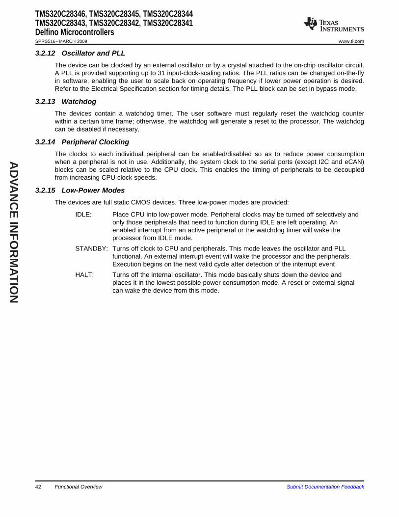
AD
VAN
CE
INF
OR
MA
TIO
N
3.2.12 Oscillator and PLL
3.2.13 Watchdog
3.2.14 Peripheral Clocking
3.2.15 Low-Power Modes
TMS320C28346, TMS320C28345, TMS320C28344TMS320C28343, TMS320C28342, TMS320C28341Delfino MicrocontrollersSPRS516–MARCH 2009 www.ti.com
The device can be clocked by an external oscillator or by a crystal attached to the on-chip oscillator circuit.A PLL is provided supporting up to 31 input-clock-scaling ratios. The PLL ratios can be changed on-the-flyin software, enabling the user to scale back on operating frequency if lower power operation is desired.Refer to the Electrical Specification section for timing details. The PLL block can be set in bypass mode.
The devices contain a watchdog timer. The user software must regularly reset the watchdog counterwithin a certain time frame; otherwise, the watchdog will generate a reset to the processor. The watchdogcan be disabled if necessary.
The clocks to each individual peripheral can be enabled/disabled so as to reduce power consumptionwhen a peripheral is not in use. Additionally, the system clock to the serial ports (except I2C and eCAN)blocks can be scaled relative to the CPU clock. This enables the timing of peripherals to be decoupledfrom increasing CPU clock speeds.
The devices are full static CMOS devices. Three low-power modes are provided:
IDLE: Place CPU into low-power mode. Peripheral clocks may be turned off selectively andonly those peripherals that need to function during IDLE are left operating. Anenabled interrupt from an active peripheral or the watchdog timer will wake theprocessor from IDLE mode.
STANDBY: Turns off clock to CPU and peripherals. This mode leaves the oscillator and PLLfunctional. An external interrupt event will wake the processor and the peripherals.Execution begins on the next valid cycle after detection of the interrupt event
HALT: Turns off the internal oscillator. This mode basically shuts down the device andplaces it in the lowest possible power consumption mode. A reset or external signalcan wake the device from this mode.
42 Functional Overview Submit Documentation Feedback

AD
VAN
CE
INF
OR
MA
TIO
N
3.2.16 Peripheral Frames 0, 1, 2, 3 (PFn)
3.2.17 General-Purpose Input/Output (GPIO) Multiplexer
3.2.18 32-Bit CPU-Timers (0, 1, 2)
TMS320C28346, TMS320C28345, TMS320C28344TMS320C28343, TMS320C28342, TMS320C28341
Delfino Microcontrollerswww.ti.com SPRS516–MARCH 2009
The device segregates peripherals into three sections. The mapping of peripherals is as follows:
PF0: PIE: PIE Interrupt Enable and Control Registers Plus PIE Vector TableXINTF: External Interface RegistersDMA DMA RegistersTimers: CPU-Timers 0, 1, 2 Registers
PF1: eCAN: eCAN Mailbox and Control RegistersGPIO: GPIO MUX Configuration and Control RegistersePWM: Enhanced Pulse Width Modulator Module and RegisterseCAP: Enhanced Capture Module and RegisterseQEP: Enhanced Quadrature Encoder Pulse Module and Registers
PF2: SYS: System Control RegistersSCI: Serial Communications Interface (SCI) Control and RX/TX RegistersSPI: Serial Port Interface (SPI) Control and RX/TX RegistersADC: External ADC InterfaceI2C: Inter-Integrated Circuit Module and RegistersXINT External Interrupt Registers
PF3: McBSP Multichannel Buffered Serial Port Registers
Most of the peripheral signals are multiplexed with general-purpose input/output (GPIO) signals. Thisenables the user to use a pin as GPIO if the peripheral signal or function is not used. On reset, GPIO pinsare configured as inputs. The user can individually program each pin for GPIO mode or peripheral signalmode. For specific inputs, the user can also select the number of input qualification cycles. This is to filterunwanted noise glitches. The GPIO signals can also be used to bring the device out of specific low-powermodes.
CPU-Timers 0, 1, and 2 are identical 32-bit timers with presettable periods and with 16-bit clockprescaling. The timers have a 32-bit count down register, which generates an interrupt when the counterreaches zero. The counter is decremented at the CPU clock speed divided by the prescale value setting.When the counter reaches zero, it is automatically reloaded with a 32-bit period value. CPU-Timer 2 isreserved for Real-Time OS (RTOS)/BIOS applications. It is connected to INT14 of the CPU. If DSP/BIOSis not being used, CPU-Timer 2 is available for general use. CPU-Timer 1 is for general use and can beconnected to INT13 of the CPU. CPU-Timer 0 is also for general use and is connected to the PIE block.
Submit Documentation Feedback Functional Overview 43

AD
VAN
CE
INF
OR
MA
TIO
N
3.2.19 Control Peripherals
3.2.20 Serial Port Peripherals
TMS320C28346, TMS320C28345, TMS320C28344TMS320C28343, TMS320C28342, TMS320C28341Delfino MicrocontrollersSPRS516–MARCH 2009 www.ti.com
The C2834x devices support the following peripherals which are used for embedded control andcommunication:
ePWM: The enhanced PWM peripheral supports independent/complementary PWMgeneration, adjustable dead-band generation for leading/trailing edges,latched/cycle-by-cycle trip mechanism. Some of the PWM pins support HRPWMfeatures.
eCAP: The enhanced capture peripheral uses a 32-bit time base and registers up to fourprogrammable events in continuous/one-shot capture modes.This peripheral can also be configured to generate an auxiliary PWM signal.
eQEP: The enhanced QEP peripheral uses a 32-bit position counter, supports low-speedmeasurement using capture unit and high-speed measurement using a 32-bit unittimer.This peripheral has a watchdog timer to detect motor stall and input error detectionlogic to identify simultaneous edge transition in QEP signals.
The devices support the following serial communication peripherals:
eCAN: This is the enhanced version of the CAN peripheral. It supports 32 mailboxes, timestamping of messages, and is CAN 2.0B-compliant.
McBSP: The multichannel buffered serial port (McBSP) connects to E1/T1 lines, phone-qualitycodecs for modem applications or high-quality stereo audio DAC devices. The McBSPreceive and transmit registers are supported by the DMA to significantly reduce theoverhead for servicing this peripheral. Each McBSP module can be configured as an SPIas required.
SPI: The SPI is a high-speed, synchronous serial I/O port that allows a serial bit stream ofprogrammed length (one to sixteen bits) to be shifted into and out of the device at aprogrammable bit-transfer rate. Normally, the SPI is used for communications between theMCU and external peripherals or another processor. Typical applications include externalI/O or peripheral expansion through devices such as shift registers, display drivers, andADCs. Multi-device communications are supported by the master/slave operation of theSPI. The SPI contains a 16-level receive and transmit FIFO for reducing interruptservicing overhead.
SCI: The serial communications interface is a two-wire asynchronous serial port, commonlyknown as UART. The SCI contains a 16-level receive and transmit FIFO for reducinginterrupt servicing overhead.
I2C: The inter-integrated circuit (I2C) module provides an interface between an MCU and otherdevices compliant with Philips Semiconductors Inter-IC bus (I2C-bus) specification version2.1 and connected by way of an I2C-bus. External components attached to this 2-wireserial bus can transmit/receive up to 8-bit data to/from the MCU through the I2C module.The I2C contains a 16-level receive and transmit FIFO for reducing interrupt servicingoverhead.
44 Functional Overview Submit Documentation Feedback

AD
VAN
CE
INF
OR
MA
TIO
N
3.3 Register Map
TMS320C28346, TMS320C28345, TMS320C28344TMS320C28343, TMS320C28342, TMS320C28341
Delfino Microcontrollerswww.ti.com SPRS516–MARCH 2009
The devices contain four peripheral register spaces. The spaces are categorized as follows:
Peripheral Frame 0: These are peripherals that are mapped directly to the CPU memory bus.See Table 3-3.
Peripheral Frame 1 These are peripherals that are mapped to the 32-bit peripheral bus. SeeTable 3-4.
Peripheral Frame 2: These are peripherals that are mapped to the 16-bit peripheral bus. SeeTable 3-5.
Peripheral Frame 3: These are peripherals that are mapped to the 32-bit DMA-accessibleperipheral bus. See Table 3-6.
Table 3-3. Peripheral Frame 0 Registers (1)
NAME ADDRESS RANGE SIZE (×16) ACCESS TYPE (2)
Device Emulation Registers 0x00 0880 - 0x00 09FF 384 EALLOW protectedCode Security Module Registers 0x00 0AE0 - 0x00 0AEF 16 EALLOW protectedXINTF Registers 0x00 0B20 - 0x00 0B3F 32 Not EALLOW protectedCPU–TIMER0/1/2 Registers 0x00 0C00 - 0x00 0C3F 64 Not EALLOW protectedPIE Registers 0x00 0CE0 - 0x00 0CFF 32 Not EALLOW protectedPIE Vector Table 0x00 0D00 - 0x00 0DFF 256 EALLOW protectedDMA Registers 0x00 1000 - 0x00 11FF 512 EALLOW protected
(1) Registers in Frame 0 support 16-bit and 32-bit accesses.(2) If registers are EALLOW protected, then writes cannot be performed until the EALLOW instruction is executed. The EDIS instruction
disables writes to prevent stray code or pointers from corrupting register contents.
Table 3-4. Peripheral Frame 1 RegistersNAME ADDRESS RANGE SIZE (×16)
eCAN-A Registers 0x00 6000 - 0x00 61FF 512eCAN-B Registers 0x00 6200 - 0x00 63FF 512ePWM1 + HRPWM1 registers 0x00 6800 - 0x00 683F 64ePWM2 + HRPWM2 registers 0x00 6840 - 0x00 687F 64ePWM3 + HRPWM3 registers 0x00 6880 - 0x00 68BF 64ePWM4 + HRPWM4 registers 0x00 68C0 - 0x00 68FF 64ePWM5 + HRPWM5 registers 0x00 6900 - 0x00 693F 64ePWM6 + HRPWM6 registers 0x00 6940 - 0x00 697F 64ePWM7 + HRPWM7 registers 0x00 6980 - 0x00 69BF 64ePWM8 + HRPWM8 registers 0x00 69C0 - 0x00 69FF 64ePWM9 + HRPWM9 registers 0x00 6600 - 0x00 663F 64eCAP1 registers 0x00 6A00 - 0x00 6A1F 32eCAP2 registers 0x00 6A20 - 0x00 6A3F 32eCAP3 registers 0x00 6A40 - 0x00 6A5F 32eCAP4 registers 0x00 6A60 - 0x00 6A7F 32eCAP5 registers 0x00 6A80 - 0x00 6A9F 32eCAP6 registers 0x00 6AA0 - 0x00 6ABF 32eQEP1 registers 0x00 6B00 - 0x00 6B3F 64eQEP2 registers 0x00 6B40 - 0x00 6B7F 64eQEP3 registers 0x00 6B80 - 0x00 6BBF 64GPIO registers 0x00 6F80 - 0x00 6FFF 128
Submit Documentation Feedback Functional Overview 45

AD
VAN
CE
INF
OR
MA
TIO
N
3.4 Device Emulation Registers
TMS320C28346, TMS320C28345, TMS320C28344TMS320C28343, TMS320C28342, TMS320C28341Delfino MicrocontrollersSPRS516–MARCH 2009 www.ti.com
Table 3-5. Peripheral Frame 2 RegistersNAME ADDRESS RANGE SIZE (×16)
System Control Registers 0x00 7010 - 0x00 702F 32SPI-A Registers 0x00 7040 - 0x00 704F 16SCI-A Registers 0x00 7050 - 0x00 705F 16External Interrupt Registers 0x00 7070 - 0x00 707F 16SCI-B Registers 0x00 7750 - 0x00 775F 16SCI-C Registers 0x00 7770 - 0x00 777F 16SPI-D Registers 0x00 7780 - 0x00 778F 16I2C-A Registers 0x00 7900 - 0x00 793F 64
Table 3-6. Peripheral Frame 3 RegistersNAME ADDRESS RANGE SIZE (×16)
McBSP-A Registers 0x00 5000 - 0x00 503F 64McBSP-B Registers 0x00 5040 - 0x00 507F 64
These registers are used to control the protection mode of the C28x CPU and to monitor some criticaldevice signals. The registers are defined in Table 3-7.
Table 3-7. Device Emulation RegistersADDRESSNAME SIZE (x16) DESCRIPTIONRANGE
0x0880DEVICECNF 2 Device Configuration Register0x0881PARTID 0x0882 1 Part ID Register TMS320C28346 0xFFD0
TMS320C28345 0xFFD1TMS320C28344 0xFFD2TMS320C28343 0xFFD3TMS320C28342 0xFFD4TMS320C28341 0xFFD5
REVID 0x0883 1 Revision ID 0x0000 - Silicon Rev. 0 - TMXRegisterPROTSTART 0x0884 1 Block Protection Start Address RegisterPROTRANGE 0x0885 1 Block Protection Range Address Register
Functional Overview46 Submit Documentation Feedback

AD
VAN
CE
INF
OR
MA
TIO
N
3.5 Interrupts
WDINT
LPMINT
Watchdog
Low Power Models
Sync
SYSCLKOUT
WAKEINT
DMAClear
Peripherals
(SPI, SCI, I2C, CAN, McBSP
)
(A),
EPWM, ECAP, EQEP
DMA
XINT1Interrupt Control
XINT1CR(15:0)
XINT1CTR(15:0)
XINT1Latch
MU
X
GPIOXINT1SEL(4:0)
DMA
XINT2Interrupt Control
XINT2CR(15:0)
XINT2CTR(15:0)
XINT2
Latch
MU
X
GPIOXINT2SEL(4:0)
DMA
TINT0CPU Timer 0
DMA
TINT2CPU Timer 2
CPU Timer 1
MU
X
TINT1
Interrupt Control
XNMICR(15:0)
XNMICTR(15:0)
MU
X
1
DMA
NMI
INT13
INT14
INT1
to
INT12
C28
Core 96
In
terru
pts
PIE
XNMI_
XINT13Latch
MU
X
GPIOXNMISEL(4:0)
GPIO
Mux
GPIO0.int
GPIO31.int
TMS320C28346, TMS320C28345, TMS320C28344TMS320C28343, TMS320C28342, TMS320C28341
Delfino Microcontrollerswww.ti.com SPRS516–MARCH 2009
Figure 3-5 shows how the various interrupt sources are multiplexed.
A. DMA-accessible
Figure 3-5. External and PIE Interrupt Sources
Submit Documentation Feedback Functional Overview 47

AD
VAN
CE
INF
OR
MA
TIO
N
Interrupt Control
XINT3CR(15:0)
Latch
Mu
x
GPIOXINT3SEL(4:0)
DMA
XINT3
Interrupt Control
XINT4CR(15:0)
Latch
Mu
x
GPIOXINT4SEL(4:0)
XINT4
Interrupt Control
XINT5CR(15:0)
Mu
x
GPIOXINT5SEL(4:0)
XINT5
Interrupt Control
XINT6CR(15:0)
Mu
x
GPIOXINT6SEL(4:0)
XINT6
Interrupt Control
XINT7CR(15:0)
Mu
x
GPIOXINT7SEL(4:0)
XINT7
DMA
DMA
DMA
DMA
96
In
terru
pts
PIE
INT1
to
INT12
C28
Core
GPIO32.int
GPIO63.int
GPIO
Mux
Latch
Latch
Latch
TMS320C28346, TMS320C28345, TMS320C28344TMS320C28343, TMS320C28342, TMS320C28341Delfino MicrocontrollersSPRS516–MARCH 2009 www.ti.com
Figure 3-6. External Interrupts
Eight PIE block interrupts are grouped into one CPU interrupt. In total, 12 CPU interrupt groups, with 8interrupts per group equals 96 possible interrupts. On the C2834x devices, 64 of these are used byperipherals as shown in Table 3-8.
The TRAP #VectorNumber instruction transfers program control to the interrupt service routinecorresponding to the vector specified. TRAP #0 attempts to transfer program control to the addresspointed to by the reset vector. The PIE vector table does not, however, include a reset vector. Therefore,TRAP #0 should not be used when the PIE is enabled. Doing so will result in undefined behavior.
When the PIE is enabled, TRAP #1 through TRAP #12 will transfer program control to the interrupt serviceroutine corresponding to the first vector within the PIE group. For example: TRAP #1 fetches the vectorfrom INT1.1, TRAP #2 fetches the vector from INT2.1, and so forth.
48 Functional Overview Submit Documentation Feedback

AD
VAN
CE
INF
OR
MA
TIO
N
INT12
MUX
INT11
INT2INT1
CPU
(Enable)(Flag)
INTx
INTx.8
PIEIERx(8:1) PIEIFRx(8:1)
MUX
INTx.7INTx.6INTx.5INTx.4INTx.3INTx.2INTx.1
FromPeripherals or
ExternalInterrupts
(Enable) (Flag)
IER(12:1)IFR(12:1)
GlobalEnable
INTM
1
0
PIEACKx
(Enable/Flag)
TMS320C28346, TMS320C28345, TMS320C28344TMS320C28343, TMS320C28342, TMS320C28341
Delfino Microcontrollerswww.ti.com SPRS516–MARCH 2009
Figure 3-7. Multiplexing of Interrupts Using the PIE Block
Table 3-8. PIE Peripheral Interrupts (1)
PIE INTERRUPTSCPU INTERRUPTS
INTx.8 INTx.7 INTx.6 INTx.5 INTx.4 INTx.3 INTx.2 INTx.1
WAKEINT TINT0INT1 Reserved XINT2 XINT1 Reserved Reserved Reserved(LPM/WD) (TIMER 0)
EPWM8_TZINT EPWM7_TZINT EPWM6_TZINT EPWM5_TZINT EPWM4_TZINT EPWM3_TZINT EPWM2_TZINT EPWM1_TZINTINT2 (ePWM8) (ePWM7) (ePWM6) (ePWM5) (ePWM4) (ePWM3) (ePWM2) (ePWM1)
EPWM8_INT EPWM7_INT EPWM6_INT EPWM5_INT EPWM4_INT EPWM3_INT EPWM2_INT EPWM1_INTINT3 (ePWM8) (ePWM7) (ePWM6) (ePWM5) (ePWM4) (ePWM3) (ePWM2) (ePWM1)
ECAP6_INT ECAP5_INT ECAP4_INT ECAP3_INT ECAP2_INT ECAP1_INTINT4 Reserved Reserved (eCAP6) (eCAP5) (eCAP4) (eCAP3) (eCAP2) (eCAP1)
EQEP3_INT EQEP2_INT EQEP1_INTINT5 Reserved Reserved Reserved Reserved Reserved (eQEP3) (eQEP2) (eQEP1)
SPITXINTD SPIRXINTD MXINTA MRINTA MXINTB MRINTB SPITXINTA SPIRXINTAINT6 (SPI-D) (SPI-D) (McBSP-A) (McBSP-A) (McBSP-B) (McBSP-B) (SPI-A) (SPI-A)
DINTCH6 DINTCH5 DINTCH4 DINTCH3 DINTCH2 DINTCH1INT7 Reserved Reserved (DMA) (DMA) (DMA) (DMA) (DMA) (DMA)
SCITXINTC SCIRXINTC I2CINT2A I2CINT1AINT8 Reserved Reserved Reserved Reserved(SCI-C) (SCI-C) (I2C-A) (I2C-A)
ECAN1_INTB ECAN0_INTB ECAN1_INTA ECAN0_INTA SCITXINTB SCIRXINTB SCITXINTA SCIRXINTAINT9 (CAN-B) (CAN-B) (CAN-A) (CAN-A) (SCI-B) (SCI-B) (SCI-A) (SCI-A)
EPWM9_TZINTINT10 Reserved Reserved Reserved Reserved Reserved Reserved Reserved (ePWM9)
EPWM9_INTINT11 Reserved Reserved Reserved Reserved Reserved Reserved Reserved (ePWM9)
LUF LVFINT12 Reserved XINT7 XINT6 XINT5 XINT4 XINT3(FPU) (FPU)
(1) Out of the 96 possible interrupts, 64 interrupts are currently used. The remaining interrupts are reserved for future devices. Theseinterrupts can be used as software interrupts if they are enabled at the PIEIFRx level, provided none of the interrupts within the group isbeing used by a peripheral. Otherwise, interrupts coming in from peripherals may be lost by accidentally clearing their flag whilemodifying the PIEIFR. To summarize, there is one sage case when the reserved interrupts could be used as software interrupts:1) No peripheral within the group is asserting interrupts.
Submit Documentation Feedback Functional Overview 49

AD
VAN
CE
INF
OR
MA
TIO
N
3.5.1 External Interrupts
TMS320C28346, TMS320C28345, TMS320C28344TMS320C28343, TMS320C28342, TMS320C28341Delfino MicrocontrollersSPRS516–MARCH 2009 www.ti.com
Table 3-9. PIE Configuration and Control RegistersNAME ADDRESS SIZE (X16) DESCRIPTION (1)
PIECTRL 0x0CE0 1 PIE, Control RegisterPIEACK 0x0CE1 1 PIE, Acknowledge RegisterPIEIER1 0x0CE2 1 PIE, INT1 Group Enable RegisterPIEIFR1 0x0CE3 1 PIE, INT1 Group Flag RegisterPIEIER2 0x0CE4 1 PIE, INT2 Group Enable RegisterPIEIFR2 0x0CE5 1 PIE, INT2 Group Flag RegisterPIEIER3 0x0CE6 1 PIE, INT3 Group Enable RegisterPIEIFR3 0x0CE7 1 PIE, INT3 Group Flag RegisterPIEIER4 0x0CE8 1 PIE, INT4 Group Enable RegisterPIEIFR4 0x0CE9 1 PIE, INT4 Group Flag RegisterPIEIER5 0x0CEA 1 PIE, INT5 Group Enable RegisterPIEIFR5 0x0CEB 1 PIE, INT5 Group Flag RegisterPIEIER6 0x0CEC 1 PIE, INT6 Group Enable RegisterPIEIFR6 0x0CED 1 PIE, INT6 Group Flag RegisterPIEIER7 0x0CEE 1 PIE, INT7 Group Enable RegisterPIEIFR7 0x0CEF 1 PIE, INT7 Group Flag RegisterPIEIER8 0x0CF0 1 PIE, INT8 Group Enable RegisterPIEIFR8 0x0CF1 1 PIE, INT8 Group Flag RegisterPIEIER9 0x0CF2 1 PIE, INT9 Group Enable RegisterPIEIFR9 0x0CF3 1 PIE, INT9 Group Flag RegisterPIEIER10 0x0CF4 1 PIE, INT10 Group Enable RegisterPIEIFR10 0x0CF5 1 PIE, INT10 Group Flag RegisterPIEIER11 0x0CF6 1 PIE, INT11 Group Enable RegisterPIEIFR11 0x0CF7 1 PIE, INT11 Group Flag RegisterPIEIER12 0x0CF8 1 PIE, INT12 Group Enable RegisterPIEIFR12 0x0CF9 1 PIE, INT12 Group Flag RegisterReserved 0x0CFA 6 Reserved
0x0CFF
(1) The PIE configuration and control registers are not protected by EALLOW mode. The PIE vector tableis protected.
Table 3-10. External Interrupt RegistersNAME ADDRESS SIZE (x16) DESCRIPTION
XINT1CR 0x00 7070 1 XINT1 configuration registerXINT2CR 0x00 7071 1 XINT2 configuration registerXINT3CR 0x00 7072 1 XINT3 configuration registerXINT4CR 0x00 7073 1 XINT4 configuration registerXINT5CR 0x00 7074 1 XINT5 configuration registerXINT6CR 0x00 7075 1 XINT6 configuration registerXINT7CR 0x00 7076 1 XINT7 configuration registerXNMICR 0x00 7077 1 XNMI configuration registerXINT1CTR 0x00 7078 1 XINT1 counter registerXINT2CTR 0x00 7079 1 XINT2 counter registerReserved 0x707A - 0x707E 5XNMICTR 0x00 707F 1 XNMI counter register
Functional Overview50 Submit Documentation Feedback

AD
VAN
CE
INF
OR
MA
TIO
N
3.6 System Control
ePWM1/../9, HRPWM1/../9,
eCAP1/../6, eQEP1/../3
Peripheral
registers
Bridge
Clock enables
I/O
Peripheral
registers
Clock enables
I/O
eCAN-A/B
/4
Peripheral
registers
Clock enables
I/O
SPI-A/D, SCI-A/B/C
LOSPCPLSPCLK
System
control
register
Bridge
SYSCLKOUT
Me
mo
ry b
us
C28x Core
GPIO
Mux
Clock enable
Peripheral
registers
I/O
McBSP-A/B
LOSPCPLSPCLK
Clock enables
Bridge
HISPCP
DM
A
bu
s
BridgeADC SOC
EXTSOC
DMAClock Enables
Pe
rip
he
ral b
us
CPU timer
registersCPU timer 0/1/2
Clock enable
Peripheral
registersI2C-A
EXTADCCLK
TMS320C28346, TMS320C28345, TMS320C28344TMS320C28343, TMS320C28342, TMS320C28341
Delfino Microcontrollerswww.ti.com SPRS516–MARCH 2009
Each external interrupt can be enabled/disabled or qualified using positive, negative, or both positive andnegative edge. For more information, see the TMS320x2834x Delfino System Control and InterruptsReference Guide (literature number SPRUFN1).
This section describes the oscillator, PLL and clocking mechanisms, the watchdog function and the lowpower modes. shows the various clock and reset domains that will be discussed.
Figure 3-8. Clock and Reset Domains
NOTEThere is a 2-SYSCLKOUT cycle delay from when the write to PCLKCR0/1/2 registers(enables peripheral clocks) occurs to when the action is valid. This delay must be takeninto account before attempting to access the peripheral configuration registers.
Submit Documentation Feedback Functional Overview 51

AD
VAN
CE
INF
OR
MA
TIO
N
3.6.1 OSC and PLL Block
X1
XCLKIN
(3.3-V clock input
from external
oscillator)
On-chiposcillator
X2
PLLSTS[OSCOFF]
OSCCLK
PLLVCOCLK
5-bit multiplier PLLCR[DIV]
OSCCLK or
VCOCLK CLKIN
OSCCLK
0
PLLSTS[PLLOFF]
nn ≠ 0
PLLSTS[DIVSEL]External
Crystal or
Resonator
To
CPU
/1
/8
/2
/4
TMS320C28346, TMS320C28345, TMS320C28344TMS320C28343, TMS320C28342, TMS320C28341Delfino MicrocontrollersSPRS516–MARCH 2009 www.ti.com
The PLL, clocking, watchdog and low-power modes, are controlled by the registers listed in Table 3-11.
Table 3-11. PLL, Clocking, Watchdog, and Low-Power Mode RegistersNAME ADDRESS SIZE (x16) DESCRIPTION
PLLSTS 0x00 7011 1 PLL Status RegisterReserved 0x00 7012 - 0x00 7018 7 ReservedPCLKCR2 0x00 7019 1 Peripheral Clock Control Register 2HISPCP 0x00 701A 1 High-Speed Peripheral Clock Pre-Scaler RegisterLOSPCP 0x00 701B 1 Low-Speed Peripheral Clock Pre-Scaler RegisterPCLKCR0 0x00 701C 1 Peripheral Clock Control Register 0PCLKCR1 0x00 701D 1 Peripheral Clock Control Register 1LPMCR0 0x00 701E 1 Low Power Mode Control Register 0Reserved 0x00 701F 1 Low Power Mode Control Register 1PCLKCR3 0x00 7020 1 Peripheral Clock Control Register 3PLLCR 0x00 7021 1 PLL Control RegisterSCSR 0x00 7022 1 System Control and Status RegisterWDCNTR 0x00 7023 1 Watchdog Counter RegisterReserved 0x00 7024 1 ReservedWDKEY 0x00 7025 1 Watchdog Reset Key RegisterReserved 0x00 7026 - 0x00 7028 3 ReservedWDCR 0x00 7029 1 Watchdog Control RegisterReserved 0x00 702A - 0x00 702C 6 ReservedEXTSOCCFG 0x00 702D 1 External ADC SOC Configuration RegisterReserved 0x00 702E 1 Reserved
Figure 3-9 shows the OSC and PLL block.
Figure 3-9. OSC and PLL Block Diagram
The on-chip oscillator circuit enables a crystal/resonator to be attached to the C2834x devices using theX1 and X2 pins. If the on-chip oscillator is not used, an external oscillator can be used in either one of thefollowing configurations:1. A 3.3-V external oscillator can be directly connected to the XCLKIN pin. The X2 pin should be left
unconnected and the X1 pin tied to VSSK. The logic-high level in this case should not exceed VDDIO.2. A 1.8-V external oscillator can be directly connected to the X1 pin. The X2 pin should be left
unconnected and the XCLKIN pin tied to VSS. The logic-high level in this case should not exceedVDD18.
Functional Overview52 Submit Documentation Feedback
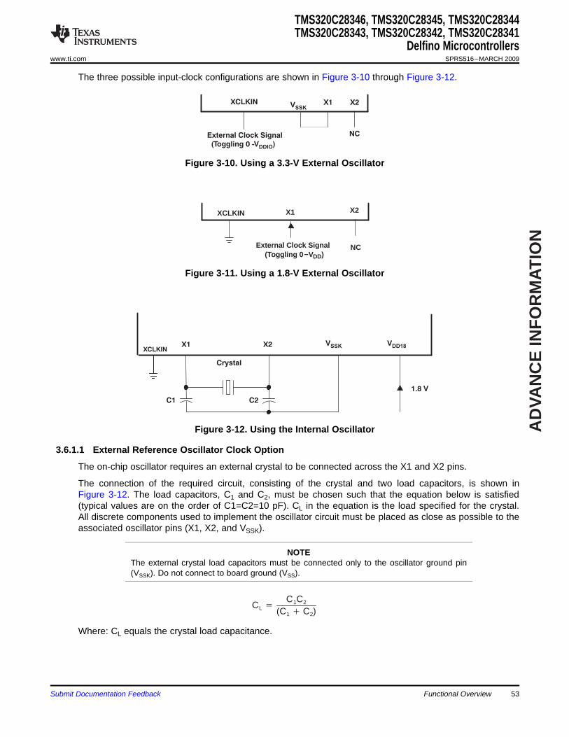
AD
VAN
CE
INF
OR
MA
TIO
N
External Clock Signal
(Toggling 0 -VDDIO
)
XCLKIN X2
NC
X1VSSK
External Clock Signal (Toggling 0 −VDD)
XCLKIN X2
NC
X1
X1 X2
C1 C2
Crystal
VSSK
VDD18
1.8 V
XCLKIN
3.6.1.1 External Reference Oscillator Clock Option
CLC1C2
(C1 C2)
TMS320C28346, TMS320C28345, TMS320C28344TMS320C28343, TMS320C28342, TMS320C28341
Delfino Microcontrollerswww.ti.com SPRS516–MARCH 2009
The three possible input-clock configurations are shown in Figure 3-10 through Figure 3-12.
Figure 3-10. Using a 3.3-V External Oscillator
Figure 3-11. Using a 1.8-V External Oscillator
Figure 3-12. Using the Internal Oscillator
The on-chip oscillator requires an external crystal to be connected across the X1 and X2 pins.
The connection of the required circuit, consisting of the crystal and two load capacitors, is shown inFigure 3-12. The load capacitors, C1 and C2, must be chosen such that the equation below is satisfied(typical values are on the order of C1=C2=10 pF). CL in the equation is the load specified for the crystal.All discrete components used to implement the oscillator circuit must be placed as close as possible to theassociated oscillator pins (X1, X2, and VSSK).
NOTEThe external crystal load capacitors must be connected only to the oscillator ground pin(VSSK). Do not connect to board ground (VSS).
Where: CL equals the crystal load capacitance.
Submit Documentation Feedback Functional Overview 53

AD
VAN
CE
INF
OR
MA
TIO
N
3.6.1.2 PLL-Based Clock Module
TMS320C28346, TMS320C28345, TMS320C28344TMS320C28343, TMS320C28342, TMS320C28341Delfino MicrocontrollersSPRS516–MARCH 2009 www.ti.com
TI recommends that customers have the crystal vendor characterize the operation of their device with theMCU chip. The crystal vendor has the equipment and expertise to tune the crystal circuit. The vendor canalso advise the customer regarding the proper component values that will produce proper start up andstability over the entire operating range.
The devices have an on-chip, PLL-based clock module. This module provides all the necessary clockingsignals for the device, as well as control for low-power mode entry. The PLL has a 5-bit ratio controlPLLCR[DIV] to select different CPU clock rates. The watchdog module should be disabled before writingto the PLLCR register. It can be re-enabled (if need be) after the PLL module has stabilized. The inputclock and PLLCR[DIV] bits should be chosen in such a way that the output frequency of the PLL(VCOCLK) falls between 400 MHz and 600 MHz. The PLLSTS[DIVSEL] bit should be selected such thatSYSCLKOUT(CLKIN) does not exceed the maximum operating frequency allowed for the device(300 MHz or 200 MHz).
Table 3-12. PLL Settings (1)
SYSCLKOUT (CLKIN)PLLCR[DIV] PLLSTS[DIVSEL] = 0 PLLSTS[DIVSEL] = 1VALUE (2) (3) PLLSTS[DIVSEL] = 2 PLLSTS[DIVSEL] = 3 (4)
00000 (PLL bypass) OSCCLK/8 (Default) OSCCLK/4 OSCCLK/2 OSCCLK00001 (OSCCLK * 2)/8 (OSCCLK * 2)/4 (OSCCLK * 2)/2 –00010 (OSCCLK * 3)/8 (OSCCLK * 3)/4 (OSCCLK * 3)/2 –00011 (OSCCLK * 4)/8 (OSCCLK * 4)/4 (OSCCLK * 4)/2 –00100 (OSCCLK * 5)/8 (OSCCLK * 5)/4 (OSCCLK * 5)/2 –00101 (OSCCLK * 6)/8 (OSCCLK * 6)/4 (OSCCLK * 6)/2 –00110 (OSCCLK * 7)/8 (OSCCLK * 7)/4 (OSCCLK * 7)/2 –00111 (OSCCLK * 8)/8 (OSCCLK * 8)/4 (OSCCLK * 8)/2 –01000 (OSCCLK * 9)/8 (OSCCLK * 9)/4 (OSCCLK * 9)/2 –01001 (OSCCLK * 10)/8 (OSCCLK * 10)/4 (OSCCLK * 10)/2 –01010 (OSCCLK * 11)/8 (OSCCLK * 11)/4 (OSCCLK * 11)/2 –
01011 - 11111 (OSCCLK * 12)/8 – (OSCCLK * 12)/4 – (OSCCLK * 12)/2 – –(OSCCLK * 32)/8 (OSCCLK * 32)/4 (OSCCLK * 32)/2
(1) PLLSTS[DIVSEL] must be 0 before writing to the PLLCR and must be set only to 2 or 3 after PLLSTS[PLLLOCKS] = 1. By default,PLLSTS[DIVSEL] is configured for /8. The boot ROM changes this to /2 or /1, depending on the boot option.
(2) The PLL control register (PLLCR) and PLL Status Register (PLLSTS) are reset to their default state by the XRS signal or a watchdogreset only. A reset issued by the debugger or the missing clock detect logic have no effect.
(3) This register is EALLOW protected. See the TMS320x2834x Delfino System Control and Interrupts Reference Guide (literature numberSPRUFN1) for more information.
(4) PLLSTS[DIVSEL] = 3 should be used only when the PLL is bypassed or off.
Table 3-13. CLKIN Divide OptionsPLLSTS [DIVSEL] CLKIN DIVIDE
0 /81 /42 /23 /1
The PLL-based clock module provides two modes of operation:• Crystal-operation - This mode allows the use of an external crystal/resonator to provide the time base
to the device.• External clock source operation - This mode allows the internal oscillator to be bypassed. The device
clocks are generated from an external clock source input on the X1 or the XCLKIN pin.
Functional Overview54 Submit Documentation Feedback

AD
VAN
CE
INF
OR
MA
TIO
N
3.6.1.3 Loss of Input Clock
3.6.2 Watchdog Block
/512OSCCLK
WDCR (WDPS[2:0])
WDCLK
WDCNTR(7:0)
WDKEY(7:0)
Good Key
1 0 1
WDCR (WDCHK[2:0])
Bad
WDCHK
Key
WDCR (WDDIS)
Clear Counter
SCSR (WDENINT)
Watchdog
Prescaler
Generate
Output Pulse
(512 OSCCLKs)
8-Bit
Watchdog
Counter
CLR
WDRST
WDINTWatchdog
55 + AA
Key Detector
XRS
Core-reset
WDRST(A)
Internal
Pullup
TMS320C28346, TMS320C28345, TMS320C28344TMS320C28343, TMS320C28342, TMS320C28341
Delfino Microcontrollerswww.ti.com SPRS516–MARCH 2009
Table 3-14. Possible PLL Configuration ModesCLKIN ANDPLL MODE REMARKS PLLSTS[DIVSEL] (1)
SYSCLKOUTInvoked by the user setting the PLLOFF bit in the PLLSTS register. The PLL block 0 OSCCLK/8is disabled in this mode. This can be useful to reduce system noise and for low 1 OSCCLK/4PLL Off power operation. The PLLCR register must first be set to 0x0000 (PLL Bypass) 2 OSCCLK/2before entering this mode. The CPU clock (CLKIN) is derived directly from the 3 OSCCLK/1input clock on either X1/X2, X1 or XCLKIN.PLL Bypass is the default PLL configuration upon power-up or after an external 0 OSCCLK/8reset (XRS). This mode is selected when the PLLCR register is set to 0x0000 or 1 OSCCLK/4PLL Bypass while the PLL locks to a new frequency after the PLLCR register has been 2 OSCCLK/2modified. In this mode, the PLL itself is bypassed but the PLL is not turned off. 3 OSCCLK/1
0 OSCCLK*n/8Achieved by writing a non-zero value n into the PLLCR register. Upon writing to the 1 OSCCLK*n/4PLL Enable PLLCR the device will switch to PLL Bypass mode until the PLL locks. 2 OSCCLK*n/2
3 – (2)
(1) PLLSTS[DIVSEL] must be 0 before writing to the PLLCR and must be set to 2 or 3 only after PLLSTS[PLLLOCKS] = 1. See theTMS320x2834x Delfino System Control and Interrupts Reference Guide (literature number SPRUFN1) for more information.
(2) PLLSTS[DIVSEL] should not be set to /1 mode while the PLL is enabled and not bypassed.
Applications in which the correct CPU operating frequency is absolutely critical should implement amechanism by which the MCU will be held in reset, should the input clocks ever fail. For example, an R-Ccircuit may be used to trigger the XRS pin of the MCU, should the capacitor ever get fully charged. An I/Opin may be used to discharge the capacitor on a periodic basis to prevent it from getting fully charged.
The watchdog block on the C2834x device is similar to the one used on the 240x and 281x devices. Thewatchdog module generates an output pulse, 512 oscillator clocks wide (OSCCLK), whenever the 8-bitwatchdog up counter has reached its maximum value. To prevent this, the user disables the counter or thesoftware must periodically write a 0x55 + 0xAA sequence into the watchdog key register which will resetthe watchdog counter. Figure 3-13 shows the various functional blocks within the watchdog module.
A. The WDRST signal is driven low for 512 OSCCLK cycles.
Figure 3-13. Watchdog Module
The WDINT signal enables the watchdog to be used as a wakeup from IDLE/STANDBY mode.
Submit Documentation Feedback Functional Overview 55

AD
VAN
CE
INF
OR
MA
TIO
N
3.7 Low-Power Modes Block
TMS320C28346, TMS320C28345, TMS320C28344TMS320C28343, TMS320C28342, TMS320C28341Delfino MicrocontrollersSPRS516–MARCH 2009 www.ti.com
In STANDBY mode, all peripherals are turned off on the device. The only peripheral that remainsfunctional is the watchdog. The WATCHDOG module will run off OSCCLK. The WDINT signal is fed to theLPM block so that it can wake the device from STANDBY (if enabled). See Section Section 3.7,Low-Power Modes Block, for more details.
In IDLE mode, the WDINT signal can generate an interrupt to the CPU, via the PIE, to take the CPU out ofIDLE mode.
In HALT mode, this feature cannot be used because the oscillator (and PLL) are turned off and hence sois the WATCHDOG.
The low-power modes on the C2834x devices devices are similar to the 240x devices. Table 3-15summarizes the various modes.
Table 3-15. Low-Power ModesMODE LPMCR0(1:0) OSCCLK CLKIN SYSCLKOUT EXIT (1)
XRS, Watchdog interrupt, any enabledIDLE 00 On On On (2)interrupt, XNMI
On XRS, Watchdog interrupt, GPIO Port ASTANDBY 01 Off Off(watchdog still running) signal, debugger (3), XNMIOff XRS, GPIO Port A signal, XNMI,HALT 1X (oscillator and PLL turned off, Off Off debugger (3)
watchdog not functional)
(1) The Exit column lists which signals or under what conditions the low power mode will be exited. A low signal, on any of the signals, willexit the low power condition. This signal must be kept low long enough for an interrupt to be recognized by the device. Otherwise theIDLE mode will not be exited and the device will go back into the indicated low power mode.
(2) The IDLE mode on the C28x behaves differently than on the 24x/240x. On the C28x, the clock output from the CPU (SYSCLKOUT) isstill functional while on the 24x/240x the clock is turned off.
(3) On the C28x, the JTAG port can still function even if the CPU clock (CLKIN) is turned off.
The various low-power modes operate as follows:
IDLE Mode: This mode is exited by any enabled interrupt or an XNMI that is recognizedby the processor. The LPM block performs no tasks during this mode aslong as the LPMCR0(LPM) bits are set to 0,0.
STANDBY Mode: Any GPIO port A signal (GPIO[31:0]) can wake the device from STANDBYmode. The user must select which signal(s) will wake the device in theGPIOLPMSEL register. The selected signal(s) are also qualified by theOSCCLK before waking the device. The number of OSCCLKs is specified inthe LPMCR0 register.
HALT Mode: Only the XRS and any GPIO port A signal (GPIO[31:0]) can wake thedevice from HALT mode. The user selects the signal in the GPIOLPMSELregister.
NOTEThe low-power modes do not affect the state of the output pins (PWM pins included).They will be in whatever state the code left them in when the IDLE instruction wasexecuted. See the TMS320x2834x Delfino System Control and Interrupts ReferenceGuide (literature number SPRUFN1) for more details.
Functional Overview56 Submit Documentation Feedback
AD
VAN
CE
INF
OR
MA
TIO
N
4 Peripherals
4.1 DMA Overview
TMS320C28346, TMS320C28345, TMS320C28344TMS320C28343, TMS320C28342, TMS320C28341
Delfino Microcontrollerswww.ti.com SPRS516–MARCH 2009
The integrated peripherals are described in the following subsections:• 6-channel Direct Memory Access (DMA)• Three 32-bit CPU-Timers• Up to nine enhanced PWM modules (ePWM1, ePWM2, ePWM3, ePWM4, ePWM5, ePWM6, ePWM7,
ePWM8, ePWM9)• Up to six enhanced capture modules (eCAP1, eCAP2, eCAP3, eCAP4, eCAP5, eCAP6)• Up to three enhanced QEP modules (eQEP1, eQEP2, eQEP3)• External analog-to-digital converter (ADC) Interface• Up to two enhanced controller area network (eCAN) modules (eCAN-A, eCAN-B)• Up to three serial communications interface modules (SCI-A, SCI-B, SCI-C)• Up to two serial peripheral interface (SPI) modules (SPI-A, SPI-D)• Inter-integrated circuit module (I2C)• Up to two multichannel buffered serial port (McBSP-A, McBSP-B) modules• Digital I/O and shared pin functions• External Interface (XINTF)
Features:• 6 Channels with independent PIE interrupts• Trigger Sources:
– McBSP-A and McBSP-B transmit and receive logic– XINT1-7 and XINT13– CPU Timers– Software
• Data Sources/Destinations:– L0-L7 64K ×16 SARAM– All XINTF zones– McBSP-A and McBSP-B transmit and receive buffers
• Word Size: 16-bit or 32-bit (McBSPs limited to 16-bit)• Throughput: 4 cycles/word (5 cycles/word for McBSP reads)
Submit Documentation Feedback Peripherals 57

AD
VAN
CE
INF
OR
MA
TIO
N
PF3
I/F
McBSP A
McBSP B
Event
triggers
DMA
6-ch
External
interrupts
CPU
timers
CPU bus
DMA bus
PIE
INT7
DIN
T[C
H1:C
H6]
CPU
XIN
TF
zones inte
rface
XIN
TF
mem
ory
zones
L0
I/FL0 RAM
L1
I/FL1 RAM
L2
I/FL2 RAM
L3
I/FL3 RAM
L4
I/FL4 RAM
L5
I/FL5 RAM
L6
I/FL6 RAM
L7
I/FL7 RAM
TMS320C28346, TMS320C28345, TMS320C28344TMS320C28343, TMS320C28342, TMS320C28341Delfino MicrocontrollersSPRS516–MARCH 2009 www.ti.com
Figure 4-1. DMA Functional Block Diagram
Peripherals58 Submit Documentation Feedback

AD
VAN
CE
INF
OR
MA
TIO
N
4.2 32-Bit CPU-Timers 0/1/2
Borrow
Reset
Timer Reload
SYSCLKOUTTCR.4
(Timer Start Status)
TINT
16-Bit Timer Divide-Down TDDRH:TDDR
32-Bit Timer PeriodPRDH:PRD
32-Bit CounterTIMH:TIM
16-Bit Prescale CounterPSCH:PSC
Borrow
INT1
to
INT12
INT14
28x
CPU
TINT2
TINT0PIE CPU-TIMER 0
CPU-TIMER 2
(Reserved for DSP/BIOS)
INT13
TINT1
CPU-TIMER 1
XINT13
TMS320C28346, TMS320C28345, TMS320C28344TMS320C28343, TMS320C28342, TMS320C28341
Delfino Microcontrollerswww.ti.com SPRS516–MARCH 2009
There are three 32-bit CPU-timers on the devices (CPU-TIMER0/1/2).
Timer 2 is reserved for DSP/BIOS™. CPU-Timer 0 and CPU-Timer 1 can be used in user applications.These timers are different from the timers that are present in the ePWM modules.
NOTENOTE: If the application is not using DSP/BIOS, then CPU-Timer 2 can be used in theapplication.
Figure 4-2. CPU-Timers
The timer interrupt signals (TINT0, TINT1, TINT2) are connected as shown in Figure 4-3.
A. The timer registers are connected to the memory bus of the C28x processor.B. The timing of the timers is synchronized to SYSCLKOUT of the processor clock.
Figure 4-3. CPU-Timer Interrupt Signals and Output Signal
The general operation of the timer is as follows: The 32-bit counter register "TIMH:TIM" is loaded with thevalue in the period register "PRDH:PRD". The counter register decrements at the SYSCLKOUT rate of theC28x. When the counter reaches 0, a timer interrupt output signal generates an interrupt pulse. Theregisters listed in Table 4-1 are used to configure the timers. For more information, see theTMS320x2834x Delfino System Control and Interrupts Reference Guide (literature number SPRUFN1).
Submit Documentation Feedback Peripherals 59

AD
VAN
CE
INF
OR
MA
TIO
N
TMS320C28346, TMS320C28345, TMS320C28344TMS320C28343, TMS320C28342, TMS320C28341Delfino MicrocontrollersSPRS516–MARCH 2009 www.ti.com
Table 4-1. CPU-Timers 0, 1, 2 Configuration and Control RegistersNAME ADDRESS SIZE (x16) DESCRIPTION
TIMER0TIM 0x0C00 1 CPU-Timer 0, Counter RegisterTIMER0TIMH 0x0C01 1 CPU-Timer 0, Counter Register HighTIMER0PRD 0x0C02 1 CPU-Timer 0, Period RegisterTIMER0PRDH 0x0C03 1 CPU-Timer 0, Period Register HighTIMER0TCR 0x0C04 1 CPU-Timer 0, Control RegisterReserved 0x0C05 1TIMER0TPR 0x0C06 1 CPU-Timer 0, Prescale RegisterTIMER0TPRH 0x0C07 1 CPU-Timer 0, Prescale Register HighTIMER1TIM 0x0C08 1 CPU-Timer 1, Counter RegisterTIMER1TIMH 0x0C09 1 CPU-Timer 1, Counter Register HighTIMER1PRD 0x0C0A 1 CPU-Timer 1, Period RegisterTIMER1PRDH 0x0C0B 1 CPU-Timer 1, Period Register HighTIMER1TCR 0x0C0C 1 CPU-Timer 1, Control RegisterReserved 0x0C0D 1TIMER1TPR 0x0C0E 1 CPU-Timer 1, Prescale RegisterTIMER1TPRH 0x0C0F 1 CPU-Timer 1, Prescale Register HighTIMER2TIM 0x0C10 1 CPU-Timer 2, Counter RegisterTIMER2TIMH 0x0C11 1 CPU-Timer 2, Counter Register HighTIMER2PRD 0x0C12 1 CPU-Timer 2, Period RegisterTIMER2PRDH 0x0C13 1 CPU-Timer 2, Period Register HighTIMER2TCR 0x0C14 1 CPU-Timer 2, Control RegisterReserved 0x0C15 1TIMER2TPR 0x0C16 1 CPU-Timer 2, Prescale RegisterTIMER2TPRH 0x0C17 1 CPU-Timer 2, Prescale Register High
0x0C18Reserved 400x0C3F
Peripherals60 Submit Documentation Feedback

AD
VAN
CE
INF
OR
MA
TIO
N
4.3 Enhanced PWM Modules (ePWM1/2/3/4/5/6/7/8/9)
0
1
EXTSOC1A
POLSEL
EXTSOC1A
EXTSOC3A
EXTSOC2A
EXTSOC1B
EXTSOC2B
EXTSOC3B
Pu
lse
Str
etc
he
r,
32
HS
PC
LK
Cy
cle
s W
ide
an
d T
he
n t
o C
hip
Pin
s
ePWM2
ePWM2SOCA
ePWM2SOCB
ePWM1
ePWM1SOCA
ePWM1SOCB
ePWM3
ePWM3SOCA
ePWM3SOCB
ePWM4
ePWM4SOCA
ePWM4SOCB
0
1
EXTSOC2A
POLSEL
ePWM6
ePWM6SOCA
ePWM6SOCB
ePWM5
ePWM5SOCA
ePWM5SOCB
ePWM7
ePWM7SOCA
ePWM7SOCB
ePWM8
ePWM8SOCA
ePWM8SOCB
0
1
EXTSOC1B
POLSEL
0
1
EXTSOC2B
POLSEL
ePWM9
ePWM9SOCA
ePWM9SOCB
0
1
EXTSOC3A
POLSEL
0
1
EXTSOC3B
POLSEL
TMS320C28346, TMS320C28345, TMS320C28344TMS320C28343, TMS320C28342, TMS320C28341
Delfino Microcontrollerswww.ti.com SPRS516–MARCH 2009
The devices contain up to nine enhanced PWM Modules (ePWM). Figure 4-4 shows a block diagram ofmultiple ePWM modules. Figure 4-4 shows the signal interconnections with the ePWM.
Table 4-2 and Table 4-3 show the complete ePWM register set per module.
Figure 4-4. Generation of SOC Pulses to the External ADC Module
Submit Documentation Feedback Peripherals 61
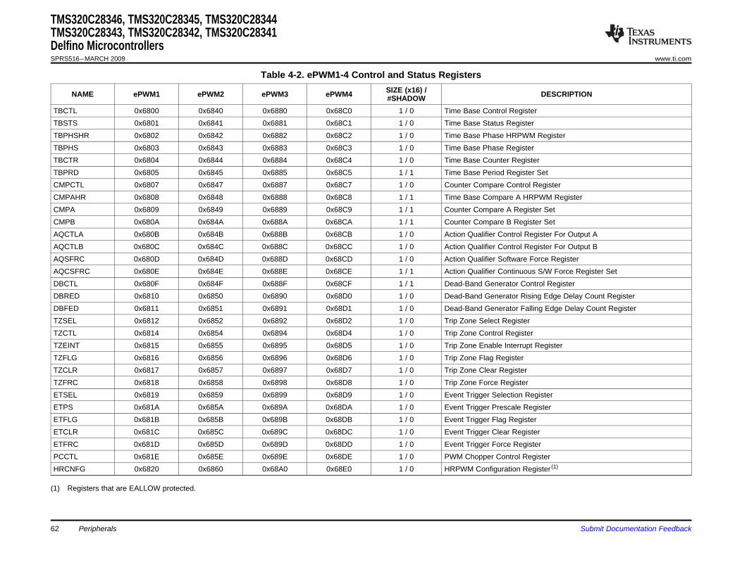
TMS320C28346, TMS320C28345, TMS320C28344TMS320C28343, TMS320C28342, TMS320C28341Delfino MicrocontrollersSPRS516–MARCH 2009 www.ti.com
Table 4-2. ePWM1-4 Control and Status RegistersSIZE (x16) /NAME ePWM1 ePWM2 ePWM3 ePWM4 DESCRIPTION#SHADOW
TBCTL 0x6800 0x6840 0x6880 0x68C0 1 / 0 Time Base Control RegisterTBSTS 0x6801 0x6841 0x6881 0x68C1 1 / 0 Time Base Status RegisterTBPHSHR 0x6802 0x6842 0x6882 0x68C2 1 / 0 Time Base Phase HRPWM RegisterTBPHS 0x6803 0x6843 0x6883 0x68C3 1 / 0 Time Base Phase RegisterTBCTR 0x6804 0x6844 0x6884 0x68C4 1 / 0 Time Base Counter RegisterTBPRD 0x6805 0x6845 0x6885 0x68C5 1 / 1 Time Base Period Register SetCMPCTL 0x6807 0x6847 0x6887 0x68C7 1 / 0 Counter Compare Control RegisterCMPAHR 0x6808 0x6848 0x6888 0x68C8 1 / 1 Time Base Compare A HRPWM RegisterCMPA 0x6809 0x6849 0x6889 0x68C9 1 / 1 Counter Compare A Register SetCMPB 0x680A 0x684A 0x688A 0x68CA 1 / 1 Counter Compare B Register SetAQCTLA 0x680B 0x684B 0x688B 0x68CB 1 / 0 Action Qualifier Control Register For Output AAQCTLB 0x680C 0x684C 0x688C 0x68CC 1 / 0 Action Qualifier Control Register For Output BAQSFRC 0x680D 0x684D 0x688D 0x68CD 1 / 0 Action Qualifier Software Force RegisterAQCSFRC 0x680E 0x684E 0x688E 0x68CE 1 / 1 Action Qualifier Continuous S/W Force Register SetDBCTL 0x680F 0x684F 0x688F 0x68CF 1 / 1 Dead-Band Generator Control RegisterDBRED 0x6810 0x6850 0x6890 0x68D0 1 / 0 Dead-Band Generator Rising Edge Delay Count RegisterDBFED 0x6811 0x6851 0x6891 0x68D1 1 / 0 Dead-Band Generator Falling Edge Delay Count RegisterTZSEL 0x6812 0x6852 0x6892 0x68D2 1 / 0 Trip Zone Select RegisterTZCTL 0x6814 0x6854 0x6894 0x68D4 1 / 0 Trip Zone Control RegisterTZEINT 0x6815 0x6855 0x6895 0x68D5 1 / 0 Trip Zone Enable Interrupt RegisterTZFLG 0x6816 0x6856 0x6896 0x68D6 1 / 0 Trip Zone Flag RegisterTZCLR 0x6817 0x6857 0x6897 0x68D7 1 / 0 Trip Zone Clear RegisterTZFRC 0x6818 0x6858 0x6898 0x68D8 1 / 0 Trip Zone Force RegisterETSEL 0x6819 0x6859 0x6899 0x68D9 1 / 0 Event Trigger Selection RegisterETPS 0x681A 0x685A 0x689A 0x68DA 1 / 0 Event Trigger Prescale RegisterETFLG 0x681B 0x685B 0x689B 0x68DB 1 / 0 Event Trigger Flag RegisterETCLR 0x681C 0x685C 0x689C 0x68DC 1 / 0 Event Trigger Clear RegisterETFRC 0x681D 0x685D 0x689D 0x68DD 1 / 0 Event Trigger Force RegisterPCCTL 0x681E 0x685E 0x689E 0x68DE 1 / 0 PWM Chopper Control RegisterHRCNFG 0x6820 0x6860 0x68A0 0x68E0 1 / 0 HRPWM Configuration Register (1)
(1) Registers that are EALLOW protected.
62 Peripherals Submit Documentation Feedback

TMS320C28346, TMS320C28345, TMS320C28344TMS320C28343, TMS320C28342, TMS320C28341
Delfino Microcontrollerswww.ti.com SPRS516–MARCH 2009
Table 4-3. ePWM5-9 Control and Status RegistersSIZE (x16) /NAME ePWM5 ePWM6 ePWM7 ePWM8 ePWM9 DESCRIPTION#SHADOW
TBCTL 0x6900 0x6940 0x6980 0x69C0 0x6600 1 / 0 Time Base Control RegisterTBSTS 0x6901 0x6941 0x6981 0x69C1 0x6601 1 / 0 Time Base Status RegisterTBPHSHR 0x6902 0x6942 0x6982 0x69C2 0x6602 1 / 0 Time Base Phase HRPWM RegisterTBPHS 0x6903 0x6943 0x6983 0x69C3 0x6603 1 / 0 Time Base Phase RegisterTBCTR 0x6904 0x6944 0x6984 0x69C4 0x6604 1 / 0 Time Base Counter RegisterTBPRD 0x6905 0x6945 0x6985 0x69C5 0x6605 1 / 1 Time Base Period Register SetCMPCTL 0x6907 0x6947 0x6987 0x69C7 0x6607 1 / 0 Counter Compare Control RegisterCMPAHR 0x6908 0x6948 0x6988 0x69C8 0x6608 1 / 1 Time Base Compare A HRPWM RegisterCMPA 0x6909 0x6949 0x6989 0x69C9 0x6609 1 / 1 Counter Compare A Register SetCMPB 0x690A 0x694A 0x698A 0x69CA 0x660A 1 / 1 Counter Compare B Register SetAQCTLA 0x690B 0x694B 0x698B 0x69CB 0x660B 1 / 0 Action Qualifier Control Register For Output AAQCTLB 0x690C 0x694C 0x698C 0x69CC 0x660C 1 / 0 Action Qualifier Control Register For Output BAQSFRC 0x690D 0x694D 0x698D 0x69CD 0x660D 1 / 0 Action Qualifier Software Force RegisterAQCSFRC 0x690E 0x694E 0x698E 0x69CE 0x660E 1 / 1 Action Qualifier Continuous S/W Force Register SetDBCTL 0x690F 0x694F 0x698F 0x69CF 0x660F 1 / 1 Dead-Band Generator Control RegisterDBRED 0x6910 0x6950 0x6990 0x69D0 0x6610 1 / 0 Dead-Band Generator Rising Edge Delay Count RegisterDBFED 0x6911 0x6951 0x6991 0x69D1 0x6611 1 / 0 Dead-Band Generator Falling Edge Delay Count RegisterTZSEL 0x6912 0x6952 0x6992 0x69D2 0x6612 1 / 0 Trip Zone Select RegisterTZCTL 0x6914 0x6954 0x6994 0x69D4 0x6614 1 / 0 Trip Zone Control RegisterTZEINT 0x6915 0x6955 0x6995 0x69D5 0x6615 1 / 0 Trip Zone Enable Interrupt RegisterTZFLG 0x6916 0x6956 0x6996 0x69D6 0x6616 1 / 0 Trip Zone Flag RegisterTZCLR 0x6917 0x6957 0x6997 0x69D7 0x6617 1 / 0 Trip Zone Clear RegisterTZFRC 0x6918 0x6958 0x6998 0x69D8 0x6618 1 / 0 Trip Zone Force RegisterETSEL 0x6919 0x6959 0x6999 0x69D9 0x6619 1 / 0 Event Trigger Selection RegisterETPS 0x691A 0x695A 0x699A 0x69DA 0x661A 1 / 0 Event Trigger Prescale RegisterETFLG 0x691B 0x695B 0x699B 0x69DB 0x661B 1 / 0 Event Trigger Flag RegisterETCLR 0x691C 0x695C 0x699C 0x69DC 0x661C 1 / 0 Event Trigger Clear RegisterETFRC 0x691D 0x695D 0x699D 0x69DD 0x661D 1 / 0 Event Trigger Force RegisterPCCTL 0x691E 0x695E 0x699E 0x69DE 0x661E 1 / 0 PWM Chopper Control RegisterHRCNFG 0x6920 0x6960 0x69A0 0x69E0 0x6620 1 / 0 HRPWM Configuration Register (1)
(1) Registers that are EALLOW protected.
Submit Documentation Feedback Peripherals 63

AD
VAN
CE
INF
OR
MA
TIO
N
CTR=PRD
TBPRD shadow (16)
TBPRD active (16)
Counter
up/down
(16 bit)
TBCTR
active (16)
TBCTL[CNTLDE]
TBCTL[SWFSYNC]
(software forced sync)
EPWMxSYNCI
CTR=ZERO
CTR_Dir
CTR=CMPB
Disabled
Sync
in/out
select
Mux
TBCTL[SYNCOSEL]
EPWMxSYNCO
TBPHS active (24)
16 8
TBPHSHR (8)
Phase
control
Time−base (TB)
CTR=CMPA
CMPA active (24)
16
CMPA shadow (24)
Action
qualifier
(AQ)
8
16
Counter compare (CC)
CMPB active (16)
CTR=CMPB
CMPB shadow (16)
CMPAHR (8)
EPWMA
EPWMB
Dead
band
(DB) (PC)
chopper
PWM
zone
(TZ)
Trip
CTR = ZERO
EPWMxAO
EPWMxBO
EPWMxTZINT
TZ1 to TZ6
HiRes PWM (HRPWM)
CTR = PRD
CTR = ZERO
CTR = CMPB
CTR = CMPA
CTR_Dir
Event
trigger
and
interrupt
(ET)
EPWMxINT
EPWMxSOCA
EPWMxSOCB
CTR=ZERO
4.4 High-Resolution PWM (HRPWM)
TMS320C28346, TMS320C28345, TMS320C28344TMS320C28343, TMS320C28342, TMS320C28341Delfino MicrocontrollersSPRS516–MARCH 2009 www.ti.com
Figure 4-5. ePWM Submodules Showing Critical Internal Signal Interconnections
The HRPWM module offers PWM resolution (time granularity) which is significantly better than what canbe achieved using conventionally derived digital PWM methods. The key points for the HRPWM moduleare:• Significantly extends the time resolution capabilities of conventionally derived digital PWM• Typically used when effective PWM resolution falls below ~ 9-10 bits. This occurs at PWM frequencies
greater than ~500 kHz when using a CPU/System clock of 300 MHz or ~375 kHz when using aCPU/system clock of 200 MHz.
• This capability can be utilized in both duty cycle and phase-shift control methods.• Finer time granularity control or edge positioning is controlled via extensions to the Compare A and
Phase registers of the ePWM module.• HRPWM capabilities are offered only on the A signal path of an ePWM module (i.e., on the EPWMxA
output). EPWMxB output has conventional PWM capabilities.
64 Peripherals Submit Documentation Feedback

AD
VAN
CE
INF
OR
MA
TIO
N
4.5 Enhanced CAP Modules (eCAP1/2/3/4/5/6)
TSCTR(counter−32 bit)
RST
CAP1(APRD active) LD
CAP2(ACMP active) LD
CAP3(APRD shadow) LD
CAP4(ACMP shadow) LD
Continuous /Oneshot
Capture Control
LD1
LD2
LD3
LD4
32
32
PRD [0−31]
CMP [0−31]
CTR [0−31]
eCAPx
InterruptTrigger
andFlag
control
to PIE
CTR=CMP
32
32
32
32
32
ACMPshadow
Event Pre-scale
CTRPHS(phase register−32 bit)
SYNCOut
SYNCIn
Eventqualifier
Polarityselect
Polarityselect
Polarityselect
Polarityselect
CTR=PRD
CTR_OVF
4
PWMcompare
logic
CTR [0−31]
PRD [0−31]
CMP [0−31]
CTR=CMP
CTR=PRD
CTR_OVFOVF
APWM mode
Delta−mode
SY
NC
4Capture events
CEVT[1:4]
APRDshadow
32
32 MO
DE
SE
LEC
T
TMS320C28346, TMS320C28345, TMS320C28344TMS320C28343, TMS320C28342, TMS320C28341
Delfino Microcontrollerswww.ti.com SPRS516–MARCH 2009
The device contains up to six enhanced capture (eCAP) modules. Figure 4-6 shows a functional blockdiagram of a module.
Figure 4-6. eCAP Functional Block Diagram
The eCAP modules are clocked at the SYSCLKOUT rate.
Submit Documentation Feedback Peripherals 65

AD
VAN
CE
INF
OR
MA
TIO
N
TMS320C28346, TMS320C28345, TMS320C28344TMS320C28343, TMS320C28342, TMS320C28341Delfino MicrocontrollersSPRS516–MARCH 2009 www.ti.com
The clock enable bits (ECAP1/2/3/4/5/6ENCLK) in the PCLKCR1 register are used to turn off the eCAPmodules individually (for low power operation). Upon reset, ECAP1ENCLK, ECAP2ENCLK,ECAP3ENCLK, ECAP4ENCLK, ECAP5ENCLK, and ECAP6ENCLK are set to low, indicating that theperipheral clock is off.
Table 4-4. eCAP Control and Status RegistersSIZENAME eCAP1 eCAP2 eCAP3 eCAP4 eCAP5 eCAP6 DESCRIPTION(x16)
TSCTR 0x6A00 0x6A20 0x6A40 0x6A60 0x6A80 0x6AA0 2 Time-Stamp CounterCTRPHS 0x6A02 0x6A22 0x6A42 0x6A62 0x6A82 0x6AA2 2 Counter Phase Offset Value
RegisterCAP1 0x6A04 0x6A24 0x6A44 0x6A64 0x6A84 0x6AA4 2 Capture 1 RegisterCAP2 0x6A06 0x6A26 0x6A46 0x6A66 0x6A86 0x6AA6 2 Capture 2 RegisterCAP3 0x6A08 0x6A28 0x6A48 0x6A68 0x6A88 0x6AA8 2 Capture 3 RegisterCAP4 0x6A0A 0x6A2A 0x6A4A 0x6A6A 0x6A8A 0x6AAA 2 Capture 4 Register
Reserved 0x6A0C- 0x6A2C- 0x6A4C- 0x6A6C- 0x6A8C- 0x6AAC- 8 Reserved0x6A12 0x6A32 0x6A52 0x6A72 0x6A92 0x6AB2
ECCTL1 0x6A14 0x6A34 0x6A54 0x6A74 0x6A94 0x6AB4 1 Capture Control Register 1ECCTL2 0x6A15 0x6A35 0x6A55 0x6A75 0x6A95 0x6AB5 1 Capture Control Register 2ECEINT 0x6A16 0x6A36 0x6A56 0x6A76 0x6A96 0x6AB6 1 Capture Interrupt Enable RegisterECFLG 0x6A17 0x6A37 0x6A57 0x6A77 0x6A97 0x6AB7 1 Capture Interrupt Flag RegisterECCLR 0x6A18 0x6A38 0x6A58 0x6A78 0x6A98 0x6AB8 1 Capture Interrupt Clear RegisterECFRC 0x6A19 0x6A39 0x6A59 0x6A79 0x6A99 0x6AB9 1 Capture Interrupt Force Register
Reserved 0x6A1A- 0x6A3A- 0x6A5A- 0x6A7A- 0x6A9A- 0x6ABA- 6 Reserved0x6A1F 0x6A3F 0x6A5F 0x6A7F 0x6A9F 0x6ABF
Peripherals66 Submit Documentation Feedback

AD
VAN
CE
INF
OR
MA
TIO
N
4.6 Enhanced QEP Modules (eQEP1/2/3)
QWDTMR
QWDPRD
16
QWDOGUTIME
QUPRD
QUTMR
32
UTOUT
WDTOUT
Quadraturecapture unit
(QCAP)QCPRDLAT
QCTMRLAT
16
QFLG
QEPSTS
QEPCTL
Registersused by
multiple units
QCLK
QDIR
QI
QS
PHE
PCSOUT
Quadraturedecoder(QDU)
QDECCTL
16
Position counter/control unit
(PCCU)QPOSLAT
QPOSSLAT
16
QPOSILAT
EQEPxAIN
EQEPxBIN
EQEPxIIN
EQEPxIOUT
EQEPxIOE
EQEPxSIN
EQEPxSOUT
EQEPxSOE
GPIOMUX
EQEPxA/XCLK
EQEPxB/XDIR
EQEPxS
EQEPxI
QPOSCMP QEINT
QFRC
32
QCLR
QPOSCTL
1632
QPOSCNT
QPOSMAX
QPOSINIT
PIEEQEPxINT
Enhanced QEP (eQEP) peripheral
Systemcontrol registers
QCTMRQCPRD
1616
QCAPCTL
EQEPxENCLK
SYSCLKOUT
Dat
a b
us
To CPU
TMS320C28346, TMS320C28345, TMS320C28344TMS320C28343, TMS320C28342, TMS320C28341
Delfino Microcontrollerswww.ti.com SPRS516–MARCH 2009
The device contains up to three enhanced quadrature encoder (eQEP) modules with 32-bit resolution.
Figure 4-7. eQEP Functional Block Diagram
Submit Documentation Feedback Peripherals 67

AD
VAN
CE
INF
OR
MA
TIO
N
TMS320C28346, TMS320C28345, TMS320C28344TMS320C28343, TMS320C28342, TMS320C28341Delfino MicrocontrollersSPRS516–MARCH 2009 www.ti.com
Table 4-5. eQEP Control and Status RegisterseQEPxeQEP1 eQEP2 eQEP3NAME SIZE(x16)/ REGISTER DESCRIPTIONADDRESS ADDRESS ADDRESS #SHADOW
QPOSCNT 0x6B00 0x6B40 0x6B80 2/0 eQEP Position CounterQPOSINIT 0x6B02 0x6B42 0x6B82 2/0 eQEP Initialization Position CountQPOSMAX 0x6B04 0x6B44 0x6B84 2/0 eQEP Maximum Position CountQPOSCMP 0x6B06 0x6B46 0x6B86 2/1 eQEP Position-compareQPOSILAT 0x6B08 0x6B48 0x6B88 2/0 eQEP Index Position LatchQPOSSLAT 0x6B0A 0x6B4A 0x6B8A 2/0 eQEP Strobe Position LatchQPOSLAT 0x6B0C 0x6B4C 0x6B8C 2/0 eQEP Position LatchQUTMR 0x6B0E 0x6B4E 0x6B8E 2/0 eQEP Unit TimerQUPRD 0x6B10 0x6B50 0x6B90 2/0 eQEP Unit Period RegisterQWDTMR 0x6B12 0x6B52 0x6B92 1/0 eQEP Watchdog TimerQWDPRD 0x6B13 0x6B53 0x6B93 1/0 eQEP Watchdog Period RegisterQDECCTL 0x6B14 0x6B54 0x6B94 1/0 eQEP Decoder Control RegisterQEPCTL 0x6B15 0x6B55 0x6B95 1/0 eQEP Control RegisterQCAPCTL 0x6B16 0x6B56 0x6B96 1/0 eQEP Capture Control RegisterQPOSCTL 0x6B17 0x6B57 0x6B97 1/0 eQEP Position-compare Control
RegisterQEINT 0x6B18 0x6B58 0x6B98 1/0 eQEP Interrupt Enable RegisterQFLG 0x6B19 0x6B59 0x6B99 1/0 eQEP Interrupt Flag RegisterQCLR 0x6B1A 0x6B5A 0x6B9A 1/0 eQEP Interrupt Clear RegisterQFRC 0x6B1B 0x6B5B 0x6B9B 1/0 eQEP Interrupt Force RegisterQEPSTS 0x6B1C 0x6B5C 0x6B9C 1/0 eQEP Status RegisterQCTMR 0x6B1D 0x6B5D 0x6B9D 1/0 eQEP Capture TimerQCPRD 0x6B1E 0x6B5E 0x6B9E 1/0 eQEP Capture Period RegisterQCTMRLAT 0x6B1F 0x6B5F 0x6B9F 1/0 eQEP Capture Timer LatchQCPRDLAT 0x6B20 0x6B60 0x6BA0 1/0 eQEP Capture Period LatchReserved 0x6B21- 0x6B3F 0x6B61- 0x6B7F 0x6BBA1 - 0x6BBF 31/0
Peripherals68 Submit Documentation Feedback
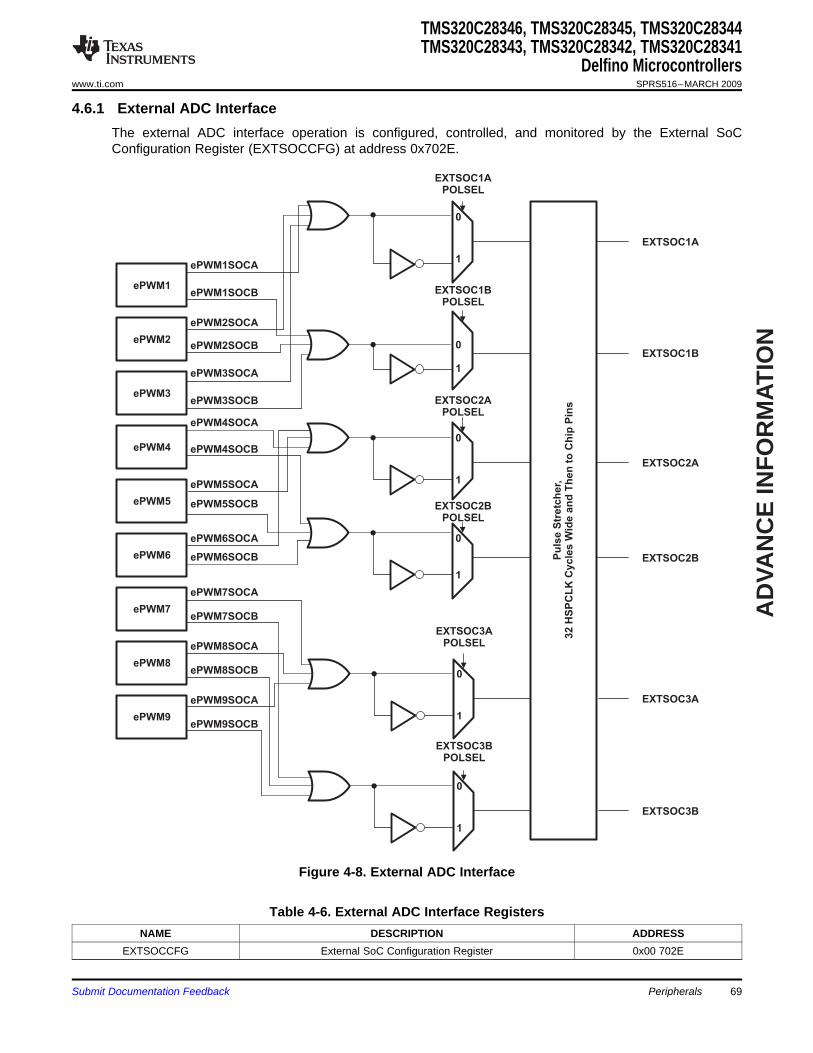
AD
VAN
CE
INF
OR
MA
TIO
N
4.6.1 External ADC Interface
0
1
EXTSOC1A
POLSEL
EXTSOC1A
EXTSOC3A
EXTSOC2A
EXTSOC1B
EXTSOC2B
EXTSOC3B
Pu
lse
Str
etc
he
r,
32
HS
PC
LK
Cy
cle
s W
ide
an
d T
he
n t
o C
hip
Pin
s
ePWM2
ePWM2SOCA
ePWM2SOCB
ePWM1
ePWM1SOCA
ePWM1SOCB
ePWM3
ePWM3SOCA
ePWM3SOCB
ePWM4
ePWM4SOCA
ePWM4SOCB
0
1
EXTSOC2A
POLSEL
ePWM6
ePWM6SOCA
ePWM6SOCB
ePWM5
ePWM5SOCA
ePWM5SOCB
ePWM7
ePWM7SOCA
ePWM7SOCB
ePWM8
ePWM8SOCA
ePWM8SOCB
0
1
EXTSOC1B
POLSEL
0
1
EXTSOC2B
POLSEL
ePWM9
ePWM9SOCA
ePWM9SOCB
0
1
EXTSOC3A
POLSEL
0
1
EXTSOC3B
POLSEL
TMS320C28346, TMS320C28345, TMS320C28344TMS320C28343, TMS320C28342, TMS320C28341
Delfino Microcontrollerswww.ti.com SPRS516–MARCH 2009
The external ADC interface operation is configured, controlled, and monitored by the External SoCConfiguration Register (EXTSOCCFG) at address 0x702E.
Figure 4-8. External ADC Interface
Table 4-6. External ADC Interface RegistersNAME DESCRIPTION ADDRESS
EXTSOCCFG External SoC Configuration Register 0x00 702E
Submit Documentation Feedback Peripherals 69
AD
VAN
CE
INF
OR
MA
TIO
N
4.7 Multichannel Buffered Serial Port (McBSP) Module
( )CLKSRG
CLKG =1+ CLKGDV
TMS320C28346, TMS320C28345, TMS320C28344TMS320C28343, TMS320C28342, TMS320C28341Delfino MicrocontrollersSPRS516–MARCH 2009 www.ti.com
The McBSP module has the following features:• Compatible to McBSP in TMS320C54x™/TMS320C55x™ DSP devices• Full-duplex communication• Double-buffered data registers that allow a continuous data stream• Independent framing and clocking for receive and transmit• External shift clock generation or an internal programmable frequency shift clock• A wide selection of data sizes including 8-, 12-, 16-, 20-, 24-, or 32-bits• 8-bit data transfers with LSB or MSB first• Programmable polarity for both frame synchronization and data clocks• Highly programmable internal clock and frame generation• Direct interface to industry-standard CODECs, Analog Interface Chips (AICs), and other serially
connected A/D and D/A devices• Works with SPI-compatible devices• The following application interfaces can be supported on the McBSP:
– T1/E1 framers– IOM-2 compliant devices– AC97-compliant devices (the necessary multiphase frame synchronization capability is provided.)– IIS-compliant devices– SPI
• McBSP clock rate,
where CLKSRG source could be LSPCLK, CLKX, or CLKR. Serial port performance is limited by I/Obuffer switching speed. Internal prescalers must be adjusted such that the peripheral speed is lessthan the I/O buffer speed limit.
NOTESee Section 6 for maximum I/O pin toggling speed.
Figure 4-9 shows the block diagram of the McBSP module.
70 Peripherals Submit Documentation Feedback

AD
VAN
CE
INF
OR
MA
TIO
N
16
McBSP Receive
Interrupt Select Logic
MDXx
MDRx
Expand Logic
DRR1 Receive Buffer
RX
Interrupt
DRR2 Receive Buffer
RBR1 RegisterRBR2 Register
MCLKXx
MFSXx
MCLKRx
MFSRx
16
Compand Logic
DXR2 Transmit Buffer
RSR1
XSR2 XSR1
Peripheral Read Bus
16
1616
1616
RSR2
DXR1 Transmit BufferLSPCLK
MRINT
To CPU
RX Interrupt Logic
McBSP Transmit
Interrupt Select Logic
TX
InterruptMXINT
To CPU TX Interrupt Logic
16
16 16
Brid
ge
DMA Bus
Pe
rip
he
ral B
us
Peripheral Write Bus
CPU
CPU
CPU
TMS320C28346, TMS320C28345, TMS320C28344TMS320C28343, TMS320C28342, TMS320C28341
Delfino Microcontrollerswww.ti.com SPRS516–MARCH 2009
Figure 4-9. McBSP Module
Table 4-7 provides a summary of the McBSP registers.
Submit Documentation Feedback Peripherals 71

AD
VAN
CE
INF
OR
MA
TIO
N
TMS320C28346, TMS320C28345, TMS320C28344TMS320C28343, TMS320C28342, TMS320C28341Delfino MicrocontrollersSPRS516–MARCH 2009 www.ti.com
Table 4-7. McBSP Register SummaryMcBSP-A McBSP-BNAME TYPE RESET VALUE DESCRIPTIONADDRESS ADDRESS
Data Registers, Receive, TransmitDRR2 0x5000 0x5040 R 0x0000 McBSP Data Receive Register 2DRR1 0x5001 0x5041 R 0x0000 McBSP Data Receive Register 1DXR2 0x5002 0x5042 W 0x0000 McBSP Data Transmit Register 2DXR1 0x5003 0x5043 W 0x0000 McBSP Data Transmit Register 1
McBSP Control RegistersSPCR2 0x5004 0x5044 R/W 0x0000 McBSP Serial Port Control Register 2SPCR1 0x5005 0x5045 R/W 0x0000 McBSP Serial Port Control Register 1RCR2 0x5006 0x5046 R/W 0x0000 McBSP Receive Control Register 2RCR1 0x5007 0x5047 R/W 0x0000 McBSP Receive Control Register 1XCR2 0x5008 0x5048 R/W 0x0000 McBSP Transmit Control Register 2XCR1 0x5009 0x5049 R/W 0x0000 McBSP Transmit Control Register 1SRGR2 0x500A 0x504A R/W 0x0000 McBSP Sample Rate Generator Register 2SRGR1 0x500B 0x504B R/W 0x0000 McBSP Sample Rate Generator Register 1
Multichannel Control RegistersMCR2 0x500C 0x504C R/W 0x0000 McBSP Multichannel Register 2MCR1 0x500D 0x504D R/W 0x0000 McBSP Multichannel Register 1RCERA 0x500E 0x504E R/W 0x0000 McBSP Receive Channel Enable Register Partition ARCERB 0x500F 0x504F R/W 0x0000 McBSP Receive Channel Enable Register Partition BXCERA 0x5010 0x5050 R/W 0x0000 McBSP Transmit Channel Enable Register Partition AXCERB 0x5011 0x5051 R/W 0x0000 McBSP Transmit Channel Enable Register Partition BPCR 0x5012 0x5052 R/W 0x0000 McBSP Pin Control RegisterRCERC 0x5013 0x5053 R/W 0x0000 McBSP Receive Channel Enable Register Partition CRCERD 0x5014 0x5054 R/W 0x0000 McBSP Receive Channel Enable Register Partition DXCERC 0x5015 0x5055 R/W 0x0000 McBSP Transmit Channel Enable Register Partition CXCERD 0x5016 0x5056 R/W 0x0000 McBSP Transmit Channel Enable Register Partition DRCERE 0x5017 0x5057 R/W 0x0000 McBSP Receive Channel Enable Register Partition ERCERF 0x5018 0x5058 R/W 0x0000 McBSP Receive Channel Enable Register Partition FXCERE 0x5019 0x5059 R/W 0x0000 McBSP Transmit Channel Enable Register Partition EXCERF 0x501A 0x505A R/W 0x0000 McBSP Transmit Channel Enable Register Partition FRCERG 0x501B 0x505B R/W 0x0000 McBSP Receive Channel Enable Register Partition GRCERH 0x501C 0x505C R/W 0x0000 McBSP Receive Channel Enable Register Partition HXCERG 0x501D 0x505D R/W 0x0000 McBSP Transmit Channel Enable Register Partition GXCERH 0x501E 0x505E R/W 0x0000 McBSP Transmit Channel Enable Register Partition HMFFINT 0x5023 0x5063 R/W 0x0000 McBSP Interrupt Enable RegisterMFFST 0x5024 0x5064 R/W 0x0000 McBSP Pin Status Register
Peripherals72 Submit Documentation Feedback

AD
VAN
CE
INF
OR
MA
TIO
N
4.8 Enhanced Controller Area Network (eCAN) Modules (eCAN-A and eCAN-B)
TMS320C28346, TMS320C28345, TMS320C28344TMS320C28343, TMS320C28342, TMS320C28341
Delfino Microcontrollerswww.ti.com SPRS516–MARCH 2009
The CAN module has the following features:• Fully compliant with CAN protocol, version 2.0B• Supports data rates up to 1 Mbps• Thirty-two mailboxes, each with the following properties:
– Configurable as receive or transmit– Configurable with standard or extended identifier– Has a programmable receive mask– Supports data and remote frame– Composed of 0 to 8 bytes of data– Uses a 32-bit time stamp on receive and transmit message– Protects against reception of new message– Holds the dynamically programmable priority of transmit message– Employs a programmable interrupt scheme with two interrupt levels– Employs a programmable alarm on transmission or reception time-out
• Low-power mode• Programmable wake-up on bus activity• Automatic reply to a remote request message• Automatic retransmission of a frame in case of loss of arbitration or error• 32-bit local network time counter synchronized by a specific message (communication in conjunction
with mailbox 16)• Self-test mode
– Operates in a loopback mode receiving its own message. A "dummy" acknowledge is provided,thereby eliminating the need for another node to provide the acknowledge bit.
NOTEFor a SYSCLKOUT of 300 MHz, the smallest bit rate possible is 11.719 kbps.
For a SYSCLKOUT of 200 MHz, the smallest bit rate possible is 7.8125 kbps.
The CAN has passed the conformance test per ISO/DIS 16845. Contact TI for test report and exceptions.
Submit Documentation Feedback Peripherals 73

AD
VAN
CE
INF
OR
MA
TIO
N
Mailbox RAM(512 Bytes)
32-Message Mailboxof 4 × 32-Bit Words
Memory ManagementUnit
CPU Interface,Receive Control Unit,
Timer Management Unit
eCAN Memory(512 Bytes)
Registers and MessageObjects Control32 32
Message Controller
32 3232 3232 32
eCAN Protocol Kernel Receive Buffer
Transmit Buffer
Control Buffer
Status Buffer
Enhanced CAN Controller32
Controls Address DataeCAN1INTeCAN0INT
32
SN65HVD23x3.3-V CAN Transceiver
CAN Bus
TMS320C28346, TMS320C28345, TMS320C28344TMS320C28343, TMS320C28342, TMS320C28341Delfino MicrocontrollersSPRS516–MARCH 2009 www.ti.com
Figure 4-10. eCAN Block Diagram and Interface Circuit
Table 4-8. 3.3-V eCAN TransceiversSUPPLY LOW-POWER SLOPEPART NUMBER VREF OTHER TAVOLTAGE MODE CONTROL
SN65HVD230Q 3.3 V Standby Adjustable Yes – -40°C to 125°CSN65HVD231Q 3.3 V Sleep Adjustable Yes – -40°C to 125°CSN65HVD232Q 3.3 V None None None – -40°C to 125°CSN65HVD233 3.3 V Standby Adjustable None Diagnostic -40°C to 125°C
LoopbackSN65HVD234 3.3 V Standby and Sleep Adjustable None – -40°C to 125°CSN65HVD235 3.3 V Standby Adjustable None Autobaud -40°C to 125°C
Loopback
Peripherals74 Submit Documentation Feedback

AD
VAN
CE
INF
OR
MA
TIO
N
Mailbox Enable − CANME
Mailbox Direction − CANMD
Transmission Request Set − CANTRS
Transmission Request Reset − CANTRR
Transmission Acknowledge − CANT A
Abort Acknowledge − CANAA
Received Message Pending − CANRMP
Received Message Lost − CANRML
Remote Frame Pending − CANRFP
Global Acceptance Mask − CANGAM
Master Control − CANMC
Bit-T iming Configuration − CANBTC
Error and Status − CANES
Transmit Error Counter − CANTEC
Receive Error Counter − CANREC
Global Interrupt Flag 0 − CANGIF0
Global Interrupt Mask − CANGIM
Mailbox Interrupt Mask − CANMIM
Mailbox Interrupt Level − CANMIL
Overwrite Protection Control − CANOPC
TX I/O Control − CANTIOC
RX I/O Control − CANRIOC
Time Stamp Counter − CANTSC
Global Interrupt Flag 1 − CANGIF1
Time-Out Control − CANT OC
Time-Out Status − CANT OS
Reserved
eCAN-A Control and Status Registers
Message Identifier − MSGID61E8h−61E9h
Message Control − MSGCTRL
Message Data Low − MDL
Message Data High − MDH
Message Mailbox (16 Bytes)
Control and Status Registers6000h
603Fh
Local Acceptance Masks (LAM)(32 × 32-Bit RAM)
6040h
607Fh
6080h
60BFh
60C0h
60FFh
eCAN-A Memory (512 Bytes)
Message Object T ime Stamps (MOTS)(32 × 32-Bit RAM)
Message Object T ime-Out (MOT O)(32 × 32-Bit RAM)
Mailbox 06100h−6107h
Mailbox 16108h−610Fh
Mailbox 26110h−6117h
Mailbox 36118h−611Fh
eCAN-A Memory RAM (512 Bytes)
Mailbox 46120h−6127h
Mailbox 2861E0h−61E7h
Mailbox 2961E8h−61EFh
Mailbox 3061F0h−61F7h
Mailbox 3161F8h−61FFh
61EAh−61EBh
61ECh−61EDh
61EEh−61EFh
TMS320C28346, TMS320C28345, TMS320C28344TMS320C28343, TMS320C28342, TMS320C28341
Delfino Microcontrollerswww.ti.com SPRS516–MARCH 2009
Figure 4-11. eCAN-A Memory Map
NOTEIf the eCAN module is not used in an application, the RAM available (LAM, MOTS,MOTO, and mailbox RAM) can be used as general-purpose RAM. The CAN module clockshould be enabled for this.
Submit Documentation Feedback Peripherals 75

AD
VAN
CE
INF
OR
MA
TIO
N
Mailbox Enable − CANME
Mailbox Direction − CANMD
Transmission Request Set − CANTRS
Transmission Request Reset − CANTRR
Transmission Acknowledge − CANT A
Abort Acknowledge − CANAA
Received Message Pending − CANRMP
Received Message Lost − CANRML
Remote Frame Pending − CANRFP
Global Acceptance Mask − CANGAM
Master Control − CANMC
Bit-T iming Configuration − CANBTC
Error and Status − CANES
Transmit Error Counter − CANTEC
Receive Error Counter − CANREC
Global Interrupt Flag 0 − CANGIF0
Global Interrupt Mask − CANGIM
Mailbox Interrupt Mask − CANMIM
Mailbox Interrupt Level − CANMIL
Overwrite Protection Control − CANOPC
TX I/O Control − CANTIOC
RX I/O Control − CANRIOC
Time Stamp Counter − CANTSC
Global Interrupt Flag 1 − CANGIF1
Time-Out Control − CANT OC
Time-Out Status − CANT OS
Reserved
eCAN-B Control and Status Registers
Message Identifier − MSGID63E8h−63E9h
Message Control − MSGCTRL
Message Data Low − MDL
Message Data High − MDH
Message Mailbox (16 Bytes)
Control and Status Registers6200h
623Fh
Local Acceptance Masks (LAM)(32 × 32-Bit RAM)
6240h
627Fh
6280h
62BFh
62C0h
62FFh
eCAN-B Memory (512 Bytes)
Message Object T ime Stamps (MOTS)(32 × 32-Bit RAM)
Message Object T ime-Out (MOT O)(32 × 32-Bit RAM)
Mailbox 06300h−6307h
Mailbox 16308h−630Fh
Mailbox 26310h−6317h
Mailbox 36318h−631Fh
eCAN-B Memory RAM (512 Bytes)
Mailbox 46320h−6327h
Mailbox 2863E0h−63E7h
Mailbox 2963E8h−63EFh
Mailbox 3063F0h−63F7h
Mailbox 3163F8h−63FFh
63EAh−63EBh
63ECh−63EDh
63EEh−63EFh
TMS320C28346, TMS320C28345, TMS320C28344TMS320C28343, TMS320C28342, TMS320C28341Delfino MicrocontrollersSPRS516–MARCH 2009 www.ti.com
Figure 4-12. eCAN-B Memory Map
The CAN registers listed in Table 4-9 are used by the CPU to configure and control the CAN controllerand the message objects. eCAN control registers only support 32-bit read/write operations. Mailbox RAMcan be accessed as 16 bits or 32 bits. 32-bit accesses are aligned to an even boundary.
Peripherals76 Submit Documentation Feedback

AD
VAN
CE
INF
OR
MA
TIO
N
TMS320C28346, TMS320C28345, TMS320C28344TMS320C28343, TMS320C28342, TMS320C28341
Delfino Microcontrollerswww.ti.com SPRS516–MARCH 2009
Table 4-9. CAN Register Map (1)
eCAN-A eCAN-B SIZEREGISTER NAME DESCRIPTIONADDRESS ADDRESS (x32)CANME 0x6000 0x6200 1 Mailbox enableCANMD 0x6002 0x6202 1 Mailbox directionCANTRS 0x6004 0x6204 1 Transmit request setCANTRR 0x6006 0x6206 1 Transmit request resetCANTA 0x6008 0x6208 1 Transmission acknowledgeCANAA 0x600A 0x620A 1 Abort acknowledge
CANRMP 0x600C 0x620C 1 Receive message pendingCANRML 0x600E 0x620E 1 Receive message lostCANRFP 0x6010 0x6210 1 Remote frame pendingCANGAM 0x6012 0x6212 1 Global acceptance maskCANMC 0x6014 0x6214 1 Master controlCANBTC 0x6016 0x6216 1 Bit-timing configurationCANES 0x6018 0x6218 1 Error and status
CANTEC 0x601A 0x621A 1 Transmit error counterCANREC 0x601C 0x621C 1 Receive error counterCANGIF0 0x601E 0x621E 1 Global interrupt flag 0CANGIM 0x6020 0x6220 1 Global interrupt maskCANGIF1 0x6022 0x6222 1 Global interrupt flag 1CANMIM 0x6024 0x6224 1 Mailbox interrupt maskCANMIL 0x6026 0x6226 1 Mailbox interrupt levelCANOPC 0x6028 0x6228 1 Overwrite protection controlCANTIOC 0x602A 0x622A 1 TX I/O controlCANRIOC 0x602C 0x622C 1 RX I/O controlCANTSC 0x602E 0x622E 1 Time stamp counter (Reserved in SCC mode)CANTOC 0x6030 0x6230 1 Time-out control (Reserved in SCC mode)CANTOS 0x6032 0x6232 1 Time-out status (Reserved in SCC mode)
(1) These registers are mapped to Peripheral Frame 1.
Submit Documentation Feedback Peripherals 77

AD
VAN
CE
INF
OR
MA
TIO
N
4.9 Serial Communications Interface (SCI) Modules (SCI-A, SCI-B, SCI-C)
Baud rate =
LSPCLK16
LSPCLK(BRR 1) * 8 when BRR ≠ 0
Baud rate = when BRR = 0
TMS320C28346, TMS320C28345, TMS320C28344TMS320C28343, TMS320C28342, TMS320C28341Delfino MicrocontrollersSPRS516–MARCH 2009 www.ti.com
The devices include three serial communications interface (SCI) modules. The SCI modules supportdigital communications between the CPU and other asynchronous peripherals that use the standardnon-return-to-zero (NRZ) format. The SCI receiver and transmitter are double-buffered, and each has itsown separate enable and interrupt bits. Both can be operated independently or simultaneously in thefull-duplex mode. To ensure data integrity, the SCI checks received data for break detection, parity,overrun, and framing errors. The bit rate is programmable to over 65000 different speeds through a 16-bitbaud-select register.
Features of each SCI module include:• Two external pins:
– SCITXD: SCI transmit-output pin– SCIRXD: SCI receive-input pin
NOTE: Both pins can be used as GPIO if not used for SCI.– Baud rate programmable to 64K different rates:
NOTESee Section 6 for maximum I/O pin toggling speed.
• Data-word format– One start bit– Data-word length programmable from one to eight bits– Optional even/odd/no parity bit– One or two stop bits
• Four error-detection flags: parity, overrun, framing, and break detection• Two wake-up multiprocessor modes: idle-line and address bit• Half- or full-duplex operation• Double-buffered receive and transmit functions• Transmitter and receiver operations can be accomplished through interrupt-driven or polled algorithms
with status flags.– Transmitter: TXRDY flag (transmitter-buffer register is ready to receive another character) and TX
EMPTY flag (transmitter-shift register is empty)– Receiver: RXRDY flag (receiver-buffer register is ready to receive another character), BRKDT flag
(break condition occurred), and RX ERROR flag (monitoring four interrupt conditions)• Separate enable bits for transmitter and receiver interrupts (except BRKDT)• NRZ (non-return-to-zero) format
NOTEAll registers in this module are 8-bit registers that are connected to Peripheral Frame 2.When a register is accessed, the register data is in the lower byte (7-0), and the upperbyte (15-8) is read as zeros. Writing to the upper byte has no effect.
Enhanced features:• Auto baud-detect hardware logic• 16-level transmit/receive FIFO
Peripherals78 Submit Documentation Feedback

AD
VAN
CE
INF
OR
MA
TIO
N
TMS320C28346, TMS320C28345, TMS320C28344TMS320C28343, TMS320C28342, TMS320C28341
Delfino Microcontrollerswww.ti.com SPRS516–MARCH 2009
The SCI port operation is configured and controlled by the registers listed in Table 4-10, Table 4-11, andTable 4-12.
Table 4-10. SCI-A Registers (1)
NAME ADDRESS SIZE (x16) DESCRIPTIONSCICCRA 0x7050 1 SCI-A Communications Control RegisterSCICTL1A 0x7051 1 SCI-A Control Register 1
SCIHBAUDA 0x7052 1 SCI-A Baud Register, High BitsSCILBAUDA 0x7053 1 SCI-A Baud Register, Low BitsSCICTL2A 0x7054 1 SCI-A Control Register 2SCIRXSTA 0x7055 1 SCI-A Receive Status Register
SCIRXEMUA 0x7056 1 SCI-A Receive Emulation Data Buffer RegisterSCIRXBUFA 0x7057 1 SCI-A Receive Data Buffer RegisterSCITXBUFA 0x7059 1 SCI-A Transmit Data Buffer RegisterSCIFFTXA (2) 0x705A 1 SCI-A FIFO Transmit RegisterSCIFFRXA (2) 0x705B 1 SCI-A FIFO Receive RegisterSCIFFCTA (2) 0x705C 1 SCI-A FIFO Control Register
SCIPRIA 0x705F 1 SCI-A Priority Control Register
(1) Registers in this table are mapped to Peripheral Frame 2 space. This space only allows 16-bit accesses. 32-bit accesses produceundefined results.
(2) These registers are new registers for the FIFO mode.
Table 4-11. SCI-B Registers (1) (2)
NAME ADDRESS SIZE (x16) DESCRIPTIONSCICCRB 0x7750 1 SCI-B Communications Control RegisterSCICTL1B 0x7751 1 SCI-B Control Register 1
SCIHBAUDB 0x7752 1 SCI-B Baud Register, High BitsSCILBAUDB 0x7753 1 SCI-B Baud Register, Low BitsSCICTL2B 0x7754 1 SCI-B Control Register 2SCIRXSTB 0x7755 1 SCI-B Receive Status Register
SCIRXEMUB 0x7756 1 SCI-B Receive Emulation Data Buffer RegisterSCIRXBUFB 0x7757 1 SCI-B Receive Data Buffer RegisterSCITXBUFB 0x7759 1 SCI-B Transmit Data Buffer RegisterSCIFFTXB (2) 0x775A 1 SCI-B FIFO Transmit RegisterSCIFFRXB (2) 0x775B 1 SCI-B FIFO Receive RegisterSCIFFCTB (2) 0x775C 1 SCI-B FIFO Control Register
SCIPRIB 0x775F 1 SCI-B Priority Control Register
(1) Registers in this table are mapped to Peripheral Frame 2 space. This space only allows 16-bit accesses. 32-bit accesses produceundefined results.
(2) These registers are new registers for the FIFO mode.
Table 4-12. SCI-C Registers (1) (2)
NAME ADDRESS SIZE (x16) DESCRIPTIONSCICCRC 0x7770 1 SCI-C Communications Control RegisterSCICTL1C 0x7771 1 SCI-C Control Register 1
SCIHBAUDC 0x7772 1 SCI-C Baud Register, High BitsSCILBAUDC 0x7773 1 SCI-C Baud Register, Low BitsSCICTL2C 0x7774 1 SCI-C Control Register 2
(1) Registers in this table are mapped to Peripheral Frame 2 space. This space only allows 16-bit accesses. 32-bit accesses produceundefined results.
(2) These registers are new registers for the FIFO mode.
Submit Documentation Feedback Peripherals 79

AD
VAN
CE
INF
OR
MA
TIO
N
TX FIFO _0
LSPCLK
WUT
Frame Format and Mode
Even/Odd EnableParity
SCI RX Interrupt select logic
BRKDT
RXRDY
SCIRXST.6
SCICTL1.3
8SCICTL2.1
RX/BK INT ENA
SCIRXD
SCIRXST.1
TXENA
SCI TX Interrupt select logic
TX EMPTY
TXRDY
SCICTL2.0
TX INT ENA
SCITXD
RXENA
SCIRXD
RXWAKE
SCICTL1.6
RX ERR INT ENA
TXWAKE
SCITXD
SCICCR.6 SCICCR.5
SCITXBUF.7-0
SCIHBAUD. 15 - 8
Baud RateMSbyteRegister
SCILBAUD. 7 - 0
Transmitter-DataBuffer Register
8 SCICTL2.6
SCICTL2.7
Baud RateLSbyte
Register
RXSHFRegister
TXSHFRegister
SCIRXST.5
1 TX FIFO _1
-----
TX FIFO _15
8
TX FIFO registers
TX FIFO
TX Interrupt
Logic
TXINT
SCIFFTX.14
RX FIFO _15
SCIRXBUF.7-0
Receive Data
Buffer register
SCIRXBUF.7-0
-----RX FIFO_1
RX FIFO _0
8
RX FIFO registers
SCICTL1.0
RX Interrupt
Logic
RXINT
RX FIFO
SCIFFRX.15
RXFFOVF
RX Error
SCIRXST.7
PEFE OERX Error
SCIRXST.4 - 2
To CPU
To CPU
AutoBaud Detect logic
SCICTL1.1
SCIFFENA
Interrupts
Interrupts
TMS320C28346, TMS320C28345, TMS320C28344TMS320C28343, TMS320C28342, TMS320C28341Delfino MicrocontrollersSPRS516–MARCH 2009 www.ti.com
Table 4-12. SCI-C Registers (continued)NAME ADDRESS SIZE (x16) DESCRIPTION
SCIRXSTC 0x7775 1 SCI-C Receive Status RegisterSCIRXEMUC 0x7776 1 SCI-C Receive Emulation Data Buffer RegisterSCIRXBUFC 0x7777 1 SCI-C Receive Data Buffer RegisterSCITXBUFC 0x7779 1 SCI-C Transmit Data Buffer RegisterSCIFFTXC (2) 0x777A 1 SCI-C FIFO Transmit RegisterSCIFFRXC (2) 0x777B 1 SCI-C FIFO Receive RegisterSCIFFCTC (2) 0x777C 1 SCI-C FIFO Control Register
SCIPRC 0x777F 1 SCI-C Priority Control Register
Figure 4-13 shows the SCI module block diagram.
Figure 4-13. Serial Communications Interface (SCI) Module Block Diagram
Peripherals80 Submit Documentation Feedback

AD
VAN
CE
INF
OR
MA
TIO
N
4.10 Serial Peripheral Interface (SPI) Module (SPI-A, SPI-D)
Baud rate =
LSPCLK4
LSPCLK(SPIBRR 1) when SPIBRR = 3 to 127
Baud rate = when SPIBRR = 0,1, 2
TMS320C28346, TMS320C28345, TMS320C28344TMS320C28343, TMS320C28342, TMS320C28341
Delfino Microcontrollerswww.ti.com SPRS516–MARCH 2009
The device includes the four-pin serial peripheral interface (SPI) module. Two SPI modules (SPI-A andSPI-D) are available. The SPI is a high-speed, synchronous serial I/O port that allows a serial bit stream ofprogrammed length (one to sixteen bits) to be shifted into and out of the device at a programmablebit-transfer rate. Normally, the SPI is used for communications between the MCU controller and externalperipherals or another processor. Typical applications include external I/O or peripheral expansion throughdevices such as shift registers, display drivers, and ADCs. Multidevice communications are supported bythe master/slave operation of the SPI.
The SPI module features include:• Four external pins:
– SPISOMI: SPI slave-output/master-input pin– SPISIMO: SPI slave-input/master-output pin– SPISTE: SPI slave transmit-enable pin– SPICLK: SPI serial-clock pin
NOTE: All four pins can be used as GPIO if the SPI module is not used.• Two operational modes: master and slave
Baud rate: 125 different programmable rates.
NOTESee Section 6 for maximum I/O pin toggling speed.
• Data word length: one to sixteen data bits• Four clocking schemes (controlled by clock polarity and clock phase bits) include:
– Falling edge without phase delay: SPICLK active-high. SPI transmits data on the falling edge of theSPICLK signal and receives data on the rising edge of the SPICLK signal.
– Falling edge with phase delay: SPICLK active-high. SPI transmits data one half-cycle ahead of thefalling edge of the SPICLK signal and receives data on the falling edge of the SPICLK signal.
– Rising edge without phase delay: SPICLK inactive-low. SPI transmits data on the rising edge of theSPICLK signal and receives data on the falling edge of the SPICLK signal.
– Rising edge with phase delay: SPICLK inactive-low. SPI transmits data one half-cycle ahead of thefalling edge of the SPICLK signal and receives data on the rising edge of the SPICLK signal.
• Simultaneous receive and transmit operation (transmit function can be disabled in software)• Transmitter and receiver operations are accomplished through either interrupt-driven or polled
algorithms.• Nine SPI module control registers: Located in control register frame beginning at address 7040h.
NOTEAll registers in this module are 16-bit registers that are connected to Peripheral Frame 2.When a register is accessed, the register data is in the lower byte (7-0), and the upperbyte (15-8) is read as zeros. Writing to the upper byte has no effect.
Enhanced feature:• 16-level transmit/receive FIFO• Delayed transmit control
Submit Documentation Feedback Peripherals 81

AD
VAN
CE
INF
OR
MA
TIO
N
TMS320C28346, TMS320C28345, TMS320C28344TMS320C28343, TMS320C28342, TMS320C28341Delfino MicrocontrollersSPRS516–MARCH 2009 www.ti.com
The SPI port operation is configured and controlled by the registers listed in Table 4-13 and Table 4-14.
Table 4-13. SPI-A RegistersNAME ADDRESS SIZE (X16) DESCRIPTION (1)
SPICCR 0x7040 1 SPI-A Configuration Control RegisterSPICTL 0x7041 1 SPI-A Operation Control RegisterSPISTS 0x7042 1 SPI-A Status RegisterSPIBRR 0x7044 1 SPI-A Baud Rate Register
SPIRXEMU 0x7046 1 SPI-A Receive Emulation Buffer RegisterSPIRXBUF 0x7047 1 SPI-A Serial Input Buffer RegisterSPITXBUF 0x7048 1 SPI-A Serial Output Buffer Register
SPIDAT 0x7049 1 SPI-A Serial Data RegisterSPIFFTX 0x704A 1 SPI-A FIFO Transmit RegisterSPIFFRX 0x704B 1 SPI-A FIFO Receive RegisterSPIFFCT 0x704C 1 SPI-A FIFO Control RegisterSPIPRI 0x704F 1 SPI-A Priority Control Register
(1) Registers in this table are mapped to Peripheral Frame 2. This space only allows 16-bit accesses. 32-bit accesses produce undefinedresults.
Table 4-14. SPI-D RegistersNAME ADDRESS SIZE (X16) DESCRIPTION (1)
SPICCR 0x7780 1 SPI-D Configuration Control RegisterSPICTL 0x7781 1 SPI-D Operation Control RegisterSPISTS 0x7782 1 SPI-D Status RegisterSPIBRR 0x7784 1 SPI-D Baud Rate Register
SPIRXEMU 0x7786 1 SPI-D Receive Emulation Buffer RegisterSPIRXBUF 0x7787 1 SPI-D Serial Input Buffer RegisterSPITXBUF 0x7788 1 SPI-D Serial Output Buffer Register
SPIDAT 0x7789 1 SPI-D Serial Data RegisterSPIFFTX 0x778A 1 SPI-D FIFO Transmit RegisterSPIFFRX 0x778B 1 SPI-D FIFO Receive RegisterSPIFFCT 0x778C 1 SPI-D FIFO Control RegisterSPIPRI 0x778F 1 SPI-D Priority Control Register
(1) Registers in this table are mapped to Peripheral Frame 2. This space only allows 16-bit accesses. 32-bit accesses produce undefinedresults.
Peripherals82 Submit Documentation Feedback

AD
VAN
CE
INF
OR
MA
TIO
N
S
SPICTL.0
SPI INT FLAG
SPI INTENA
SPISTS.6
S
ClockPolarity
Talk
LSPCLK
456 123 0
0123
SPI Bit Rate
State Control
SPIRXBUFBuffer Register
ClockPhase
ReceiverOverrun Flag
SPICTL.4
OverrunINT ENA
SPICCR.3 − 0
SPIBRR.6 − 0 SPICCR.6 SPICTL.3
SPIDAT.15 − 0
SPICTL.1
M
S
M
Master/Slave
SPISTS.7
SPIDATData Register
M
S
SPICTL.2SPI Char
SPISIMO
SPISOMI
SPICLK
SW2
S
M
M
S
SW3
To CPU
M
SW1
SPITXBUF
Buffer Register
RX FIFO _0
RX FIFO _1
−−−−−
RX FIFO _15
TX FIFO registers
TX FIFO _0
TX FIFO _1−−−−−
TX FIFO _15
RX FIFO registers
16
16
16
TX InterruptLogic
RX InterruptLogic
SPIINT/SPIRXINT
SPITXINT
SPIFFOVF FLAG
SPIFFRX.15
16
TX FIFO Interrupt
RX FIFO Interrupt
SPIRXBUF
SPITXBUF
SPIFFTX.14
SPIFFENA
SPISTE(A)
TMS320C28346, TMS320C28345, TMS320C28344TMS320C28343, TMS320C28342, TMS320C28341
Delfino Microcontrollerswww.ti.com SPRS516–MARCH 2009
Figure 4-14 is a block diagram of the SPI in slave mode.
A. SPISTE is driven low by the master for a slave device.
Figure 4-14. SPI Module Block Diagram (Slave Mode)
Submit Documentation Feedback Peripherals 83

AD
VAN
CE
INF
OR
MA
TIO
N
4.11 Inter-Integrated Circuit (I2C)
SYSRS
Data[16]
SYSCLKOUT
Data[16]
Addr[16]
Control
I2CINT1A
I2CINT2A
C28X CPU
GPIOMUX
I2C−A
System ControlBlock
I2CAENCLK
PIEBlock
SDAA
SCLA
Per
iphe
ral B
us
TMS320C28346, TMS320C28345, TMS320C28344TMS320C28343, TMS320C28342, TMS320C28341Delfino MicrocontrollersSPRS516–MARCH 2009 www.ti.com
The device contains one I2C Serial Port. Figure 4-15 shows how the I2C peripheral module interfaceswithin the device.
A. The I2C registers are accessed at the SYSCLKOUT rate. The internal timing and signal waveforms of the I2C port arealso at the SYSCLKOUT rate.
B. The clock enable bit (I2CAENCLK) in the PCLKCR0 register turns off the clock to the I2C port for low poweroperation. Upon reset, I2CAENCLK is clear, which indicates the peripheral internal clocks are off.
Figure 4-15. I2C Peripheral Module Interfaces
The I2C module has the following features:• Compliance with the Philips Semiconductors I2C-bus specification (version 2.1):
– Support for 1-bit to 8-bit format transfers– 7-bit and 10-bit addressing modes– General call– START byte mode– Support for multiple master-transmitters and slave-receivers– Support for multiple slave-transmitters and master-receivers– Combined master transmit/receive and receive/transmit mode– Data transfer rate of from 10 kbps up to 400 kbps (Philips Fast-mode rate)
• One 16-word receive FIFO and one 16-word transmit FIFO• One interrupt that can be used by the CPU. This interrupt can be generated as a result of one of the
following conditions:– Transmit-data ready– Receive-data ready– Register-access ready– No-acknowledgment received
Peripherals84 Submit Documentation Feedback

AD
VAN
CE
INF
OR
MA
TIO
N
4.12 GPIO MUX
TMS320C28346, TMS320C28345, TMS320C28344TMS320C28343, TMS320C28342, TMS320C28341
Delfino Microcontrollerswww.ti.com SPRS516–MARCH 2009
– Arbitration lost– Stop condition detected– Addressed as slave
• An additional interrupt that can be used by the CPU when in FIFO mode• Module enable/disable capability• Free data format mode
The registers in Table 4-15 configure and control the I2C port operation.
Table 4-15. I2C-A RegistersNAME ADDRESS DESCRIPTION
I2COAR 0x7900 I2C own address registerI2CIER 0x7901 I2C interrupt enable registerI2CSTR 0x7902 I2C status registerI2CCLKL 0x7903 I2C clock low-time divider registerI2CCLKH 0x7904 I2C clock high-time divider registerI2CCNT 0x7905 I2C data count registerI2CDRR 0x7906 I2C data receive registerI2CSAR 0x7907 I2C slave address registerI2CDXR 0x7908 I2C data transmit registerI2CMDR 0x7909 I2C mode registerI2CISRC 0x790A I2C interrupt source registerI2CPSC 0x790C I2C prescaler registerI2CFFTX 0x7920 I2C FIFO transmit registerI2CFFRX 0x7921 I2C FIFO receive registerI2CRSR - I2C receive shift register (not accessible to the CPU)I2CXSR - I2C transmit shift register (not accessible to the CPU)
On the 2834x devices, the GPIO MUX can multiplex up to three independent peripheral signals on asingle GPIO pin in addition to providing individual pin bit-banging IO capability. The GPIO MUX blockdiagram per pin is shown in Figure 4-16. Because of the open drain capabilities of the I2C pins, the GPIOMUX block diagram for these pins differ. See the TMS320x2834x Delfino System Control and InterruptsReference Guide (literature number SPRUFN1) for details.
NOTEThere is a 2-SYSCLKOUT cycle delay from when the write to the GPxMUXn andGPxQSELn registers occurs to when the action is valid.
Submit Documentation Feedback Peripherals 85

AD
VAN
CE
INF
OR
MA
TIO
N
GPxDAT (read)
Input
Qualification
GPxMUX1/2
High Impedance
Output Control
GPIOx pin
XRS
0 = Input, 1 = Output
Low PowerModes Block
GPxDIR (latch)
Peripheral 2 Input
Peripheral 3 Input
Peripheral 1 Output
Peripheral 2 Output
Peripheral 3 Output
Peripheral 1 Output Enable
Peripheral 2 Output Enable
Peripheral 3 Output Enable
00
01
10
11
00
01
10
11
00
01
10
11
GPxCTRL
Peripheral 1 Input
N/CGPxPUD
LPMCR0
Internal
Pullup
GPIOLMPSEL
GPxQSEL1/2
GPxSET
GPxDAT (latch)
GPxCLEAR
GPxTOGGLE
GPIOXINT7SEL
GPIOXNMISEL
= Default at Reset
PIEExternal Interrupt
MUX
Asynchronous
path
Asynchronous path
GPIOXINT1SEL
GPIOXINT2SEL
GPIOXINT3SEL
TMS320C28346, TMS320C28345, TMS320C28344TMS320C28343, TMS320C28342, TMS320C28341Delfino MicrocontrollersSPRS516–MARCH 2009 www.ti.com
A. x stands for the port, either A or B. For example, GPxDIR refers to either the GPADIR and GPBDIR registerdepending on the particular GPIO pin selected.
B. GPxDAT latch/read are accessed at the same memory location.C. This is a generic GPIO MUX block diagram. Not all options may be applicable for all GPIO pins. See the
TMS320x2834x Delfino System Control and Interrupts Reference Guide (literature number SPRUFN1) for pin-specificvariations.
Figure 4-16. GPIO MUX Block Diagram
86 Peripherals Submit Documentation Feedback

AD
VAN
CE
INF
OR
MA
TIO
N
TMS320C28346, TMS320C28345, TMS320C28344TMS320C28343, TMS320C28342, TMS320C28341
Delfino Microcontrollerswww.ti.com SPRS516–MARCH 2009
The device supports 88 GPIO pins. The GPIO control and data registers are mapped to PeripheralFrame 1 to enable 32-bit operations on the registers (along with 16-bit operations). Table 4-16 shows theGPIO register mapping.
Table 4-16. GPIO RegistersNAME ADDRESS SIZE (x16) DESCRIPTION
GPIO CONTROL REGISTERS (EALLOW PROTECTED)GPACTRL 0x6F80 2 GPIO A Control Register (GPIO0 to 31)
GPAQSEL1 0x6F82 2 GPIO A Qualifier Select 1 Register (GPIO0 to 15)GPAQSEL2 0x6F84 2 GPIO A Qualifier Select 2 Register (GPIO16 to 31)GPAMUX1 0x6F86 2 GPIO A MUX 1 Register (GPIO0 to 15)GPAMUX2 0x6F88 2 GPIO A MUX 2 Register (GPIO16 to 31)GPADIR 0x6F8A 2 GPIO A Direction Register (GPIO0 to 31)GPAPUD 0x6F8C 2 GPIO A Pull Up Disable Register (GPIO0 to 31)Reserved 0x6F8E – 0x6F8F 2GPBCTRL 0x6F90 2 GPIO B Control Register (GPIO32 to 35)
GPBQSEL1 0x6F92 2 GPIO B Qualifier Select 1 Register (GPIO32 to 35)GPBQSEL2 0x6F94 2 ReservedGPBMUX1 0x6F96 2 GPIO B MUX 1 Register (GPIO32 to 35)GPBMUX2 0x6F98 2 GPIO B MUX 2 Register (GPIO48 to 63)GPBDIR 0x6F9A 2 GPIO B Direction Register (GPIO32 to 35)GPBPUD 0x6F9C 2 GPIO B Pull Up Disable Register (GPIO32 to 35)Reserved 0x6F9E – 0x6FA5 8
GPCMUX1 0x6FA6 2 GPIO C MUX1 Register (GPIO64 to 79)GPCMUX2 0x6FA8 2 GPIO C MUX2 Register (GPIO80 to 87)GPCDIR 0x6FAA 2 GPIO C Direction Register (GPIO64 to 87)GPCPUD 0x6FAC 2 GPIO C Pull Up Disable Register (GPIO64 to 87)Reserved 0x6FAE – 0x6FBF 18
GPIO DATA REGISTERS (NOT EALLOW PROTECTED)GPADAT 0x6FC0 2 GPIO A Data Register (GPIO0 to 31)GPASET 0x6FC2 2 GPIO A Data Set Register (GPIO0 to 31)
GPACLEAR 0x6FC4 2 GPIO A Data Clear Register (GPIO0 to 31)GPATOGGLE 0x6FC6 2 GPIO A Data Toggle Register (GPIO0 to 31)
GPBDAT 0x6FC8 2 GPIO B Data Register (GPIO32 to 35)GPBSET 0x6FCA 2 GPIO B Data Set Register (GPIO32 to 35)
GPBCLEAR 0x6FCC 2 GPIO B Data Clear Register (GPIO32 to 35)GPBTOGGLE 0x6FCE 2 GPIOB Data Toggle Register (GPIO32 to 35)
GPCDAT 0x6FD0 2 GPIO C Data Register (GPIO64 to 87)GPCSET 0x6FD2 2 GPIO C Data Set Register (GPIO64 to 87)
GPCCLEAR 0x6FD4 2 GPIO C Data Clear Register (GPIO64 to 87)GPCTOGGLE 0x6FD6 2 GPIO C Data Toggle Register (GPIO64 to 87)
Reserved 0x6FD8 0x6FDF 8GPIO INTERRUPT AND LOW POWER MODES SELECT REGISTERS (EALLOW PROTECTED)
GPIOXINT1SEL 0x6FE0 1 XINT1 GPIO Input Select Register (GPIO0 to 31)GPIOXINT2SEL 0x6FE1 1 XINT2 GPIO Input Select Register (GPIO0 to 31)GPIOXNMISEL 0x6FE2 1 XNMI GPIO Input Select Register (GPIO0 to 31)GPIOXINT3SEL 0x6FE3 1 XINT3 GPIO Input Select Register (GPIO32 to 63)GPIOXINT4SEL 0x6FE4 1 XINT4 GPIO Input Select Register (GPIO32 to 63)GPIOXINT5SEL 0x6FE5 1 XINT5 GPIO Input Select Register (GPIO32 to 63)
Submit Documentation Feedback Peripherals 87

AD
VAN
CE
INF
OR
MA
TIO
N
TMS320C28346, TMS320C28345, TMS320C28344TMS320C28343, TMS320C28342, TMS320C28341Delfino MicrocontrollersSPRS516–MARCH 2009 www.ti.com
Table 4-16. GPIO Registers (continued)NAME ADDRESS SIZE (x16) DESCRIPTION
GPIOXINT6SEL 0x6FE6 1 XINT6 GPIO Input Select Register (GPIO32 to 63)GPIOINT7SEL 0x6FE7 1 XINT7 GPIO Input Select Register (GPIO32 to 63)GPIOLPMSEL 0x6FE8 2 LPM GPIO Select Register (GPIO0 to 31)
Reserved 0x6FEA – 0x6FFF 22
Table 4-17. GPIO-A Mux Peripheral Selection MatrixREGISTER BITS PERIPHERAL SELECTION
GPADIRGPADAT GPAMUX1 GPIOx PER1 PER2 PER3GPASET GPAQSEL1 GPAMUX1=0,0 GPAMUX1 = 0, 1 GPAMUX1 = 1, 0 GPAMUX1 = 1, 1GPACLR
GPATOGGLEQUALPRD0 0 1, 0 GPIO0 (I/O) EPWM1A (O) Reserved Reserved
1 3, 2 GPIO1 (I/O) EPWM1B (O) ECAP6 (I/O) MFSRB (I/O)2 5, 4 GPIO2 (I/O) EPWM2A (O) Reserved Reserved3 7, 6 GPIO3 (I/O) EPWM2B (O) ECAP5 (I/O) MCLKRB (I/O)4 9, 8 GPIO4 (I/O) EPWM3A (O) Reserved Reserved5 11, 10 GPIO5 (I/O) EPWM3B (O) MFSRA (I/O) ECAP1 (I/O)6 13, 12 GPIO6 (I/O) EPWM4A (O) EPWMSYNCI (I) EPWMSYNCO (O)7 15, 14 GPIO7 (I/O) EPWM4B (O) MCLKRA (I/O) ECAP2 (I/O)
QUALPRD1 8 17, 16 GPIO8 (I/O) EPWM5A (O) CANTXB (O) ADCSOCAO (O)9 19, 18 GPIO9 (I/O) EPWM5B (O) SCITXDB (O) ECAP3 (I/O)
10 21, 20 GPIO10 (I/O) EPWM6A (O) CANRXB (I) ADCSOCBO (O)11 23, 22 GPIO11 (I/O) EPWM6B (O) SCIRXDB (I) ECAP4 (I/O)12 25, 24 GPIO12 (I/O) TZ1 (I) CANTXB (O) MDXB (O)13 27, 26 GPIO13 (I/O) TZ2 (I) CANRXB (I) MDRB (I)14 29, 28 GPIO14 (I/O) TZ3 (I)/XHOLD (I) SCITXDB (O) MCLKXB (I/O)15 31, 30 GPIO15 (I/O) TZ4 (I)/XHOLDA (O) SCIRXDB (I) MFSXB (I/O)
GPAMUX2 GPAMUX2 =0, 0 GPAMUX2 = 0, 1 GPAMUX2 = 1, 0 GPAMUX2 = 1, 1GPAQSEL2QUALPRD2 16 1, 0 GPIO16 (I/O) SPISIMOA (I/O) CANTXB (O) TZ5 (I)
17 3, 2 GPIO17 (I/O) SPISOMIA (I/O) CANRXB (I) TZ6 (I)18 5, 4 GPIO18 (I/O) SPICLKA (I/O) SCITXDB (O) CANRXA (I)19 7, 6 GPIO19 (I/O) SPISTEA (I/O) SCIRXDB (I) CANTXA (O)20 9, 8 GPIO20 (I/O) EQEP1A (I) MDXA (O) CANTXB (O)21 11, 10 GPIO21 (I/O) EQEP1B (I) MDRA (I) CANRXB (I)22 13, 12 GPIO22 (I/O) EQEP1S (I/O) MCLKXA (I/O) SCITXDB (O)23 15, 14 GPIO23 (I/O) EQEP1I (I/O) MFSXA (I/O) SCIRXDB (I)
QUALPRD3 24 17, 16 GPIO24 (I/O) ECAP1 (I/O) EQEP2A (I) MDXB (O)25 19, 18 GPIO25 (I/O) ECAP2 (I/O) EQEP2B (I) MDRB (I)26 21, 20 GPIO26 (I/O) ECAP3 (I/O) EQEP2I (I/O) MCLKXB (I/O)27 23, 22 GPIO27 (I/O) ECAP4 (I/O) EQEP2S (I/O) MFSXB (I/O)28 25, 24 GPIO28 (I/O) SCIRXDA (I) XZCS6 (O)29 27, 26 GPIO29 (I/O) SCITXDA (O) XA19 (O)30 29, 28 GPIO30 (I/O) CANRXA (I) XA18 (O)31 31, 30 GPIO31 (I/O) CANTXA (O) XA17 (O)
Peripherals88 Submit Documentation Feedback

AD
VAN
CE
INF
OR
MA
TIO
N
TMS320C28346, TMS320C28345, TMS320C28344TMS320C28343, TMS320C28342, TMS320C28341
Delfino Microcontrollerswww.ti.com SPRS516–MARCH 2009
Table 4-18. GPIO-B Mux Peripheral Selection MatrixREGISTER BITS PERIPHERAL SELECTION
GPBDIRGPBDAT GPBMUX1 GPIOx PER1 PER2 PER3GPBSET GPBQSEL1 GPBMUX1=0, 0 GPBMUX1 = 0, 1 GPBMUX1 = 1, 0 GPBMUX1 = 1, 1GPBCLR
GPBTOGGLEQUALPRD0 0 1, 0 GPIO32 (I/O) SDAA (I/OC) (1) EPWMSYNCI (I) ADCSOCAO (O)
1 3, 2 GPIO33 (I/O) SCLA (I/OC) (1) EPWMSYNCO (O) ADCSOCBO (O)2 5, 4 GPIO34 (I/O) ECAP1 (I/O) XREADY (I)3 7, 6 GPIO35 (I/O) SCITXDA (O) XR/W (O)4 9, 8 GPIO36 (I/O) SCIRXDA (I) XZCS0 (O)5 11, 10 GPIO37 (I/O) ECAP2 (I/O) XZCS7 (O)6 13, 12 GPIO38 (I/O) XWE0 (O)7 15, 14 GPIO39 (I/O) XA16 (O)
QUALPRD1 8 17, 16 GPIO40 (I/O) XA0 (O)9 19, 18 GPIO41 (I/O) XA1 (O)10 21, 20 GPIO42 (I/O) XA2 (O)
Reserved11 23, 22 GPIO43 (I/O) XA3 (O)12 25, 24 GPIO44 (I/O) XA4 (O)13 27, 26 GPIO45 (I/O) XA5 (O)14 29, 28 GPIO46 (I/O) XA6 (O)15 31, 30 GPIO47 (I/O) XA7 (O)
GPBMUX2 GPBMUX2 =0, 0 GPBMUX2 = 0, 1 GPBMUX2 = 1, 0 GPBMUX2 = 1, 1GPBQSEL2QUALPRD2 16 1, 0 GPIO48 (I/O) ECAP5 (I/O) XD31 (I/O) SPISIMOD (I/O)
17 3, 2 GPIO49 (I/O) ECAP6 (I/O) XD30 (I/O) SPISOMID (I/O)18 5, 4 GPIO50 (I/O) EQEP1A (I) XD29 (I/O) SPICLKD (I/O)19 7, 6 GPIO51 (I/O) EQEP1B (I) XD28 (I/O) SPISTED (I/O)20 9, 8 GPIO52 (I/O) EQEP1S (I/O) XD27 (I/O) Reserved21 11, 10 GPIO53 (I/O) EQEP1I (I/O) XD26 (I/O) Reserved22 13, 12 GPIO54 (I/O) SPISIMOA (I/O) XD25 (I/O) EQEP3A (I)23 15, 14 GPIO55 (I/O) SPISOMIA (I/O) XD24 (I/O) EQEP3B (I)
QUALPRD3 24 17, 16 GPIO56 (I/O) SPICLKA (I/O) XD23 (I/O) EQEP3S (I/O)25 19, 18 GPIO57 (I/O) SPISTEA (I/O) XD22 (I/O) EQEP3I (I/O)26 21, 20 GPIO58 (I/O) MCLKRA (I/O) XD21 (I/O) EPWM7A (O)27 23, 22 GPIO59 (I/O) MFSRA (I/O) XD20 (I/O) EPWM7B (O)28 25, 24 GPIO60 (I/O) MCLKRB (I/O) XD19 (I/O) EPWM8A (O)29 27, 26 GPIO61 (I/O) MFSRB (I/O) XD18 (I/O) EPWM8B (O)30 29, 28 GPIO62 (I/O) SCIRXDC (I) XD17 (I/O) EPWM9A (O)31 31, 30 GPIO63 (I/O) SCITXDC (O) XD16 (I/O) EPWM9B (O)
(1) Open drain
Submit Documentation Feedback Peripherals 89

AD
VAN
CE
INF
OR
MA
TIO
N
TMS320C28346, TMS320C28345, TMS320C28344TMS320C28343, TMS320C28342, TMS320C28341Delfino MicrocontrollersSPRS516–MARCH 2009 www.ti.com
Table 4-19. GPIO-C Mux Peripheral Selection MatrixREGISTER BITS PERIPHERAL SELECTION
GPCDIRGPCDAT GPIOx or PER1 PER2 or PER3GPCSET GPCMUX1 GPCMUX1 = 0, 0 or 0, 1 GPCMUX1 = 1, 0 or 1, 1GPCCLR
GPCTOGGLEno qual 0 1, 0 GPIO64 (I/O) XD15 (I/O)
1 3, 2 GPIO65 (I/O) XD14 (I/O)2 5, 4 GPIO66 (I/O) XD13 (I/O)3 7, 6 GPIO67 (I/O) XD12 (I/O)4 9, 8 GPIO68 (I/O) XD11 (I/O)5 11, 10 GPIO69 (I/O) XD10 (I/O)6 13, 12 GPIO70 (I/O) XD9 (I/O)7 15, 14 GPIO71 (I/O) XD8 (I/O)
no qual 8 17, 16 GPIO72 (I/O) XD7 (I/O)9 19, 18 GPIO73 (I/O) XD6 (I/O)10 21, 20 GPIO74 (I/O) XD5 (I/O)11 23, 22 GPIO75 (I/O) XD4 (I/O)12 25, 24 GPIO76 (I/O) XD3 (I/O)13 27, 26 GPIO77 (I/O) XD2 (I/O)14 29, 28 GPIO78 (I/O) XD1 (I/O)15 31, 30 GPIO79 (I/O) XD0 (I/O)
GPCMUX2 GPCMUX2 = 0, 0 or 0, 1 GPCMUX2 = 1, 0 or 1, 1no qual 16 1, 0 GPIO80 (I/O) XA8 (O)
17 3, 2 GPIO81 (I/O) XA9 (O)18 5, 4 GPIO82 (I/O) XA10 (O)19 7, 6 GPIO83 (I/O) XA11 (O)20 9, 8 GPIO84 (I/O) XA12 (O)21 11, 10 GPIO85 (I/O) XA13 (O)22 13, 12 GPIO86 (I/O) XA14 (O)23 15, 14 GPIO87 (I/O) XA15 (O)
The user can select the type of input qualification for each GPIO pin via the GPxQSEL1/2 registers fromfour choices:• Synchronization To SYSCLKOUT Only (GPxQSEL1/2=0, 0): This is the default mode of all GPIO pins
at reset and it simply synchronizes the input signal to the system clock (SYSCLKOUT).• Qualification Using Sampling Window (GPxQSEL1/2=0, 1 and 1, 0): In this mode the input signal, after
synchronization to the system clock (SYSCLKOUT), is qualified by a specified number of cycles beforethe input is allowed to change.
90 Peripherals Submit Documentation Feedback

AD
VAN
CE
INF
OR
MA
TIO
N
GPyCTRL Reg
SYNC
SYSCLKOUT
Qualification Input Signal Qualified By 3 or 6 Samples
GPIOx
Time between samples
GPxQSEL
Number of Samples
TMS320C28346, TMS320C28345, TMS320C28344TMS320C28343, TMS320C28342, TMS320C28341
Delfino Microcontrollerswww.ti.com SPRS516–MARCH 2009
Figure 4-17. Qualification Using Sampling Window
• The sampling period is specified by the QUALPRD bits in the GPxCTRL register and is configurable ingroups of 8 signals. It specifies a multiple of SYSCLKOUT cycles for sampling the input signal. Thesampling window is either 3-samples or 6-samples wide and the output is only changed when ALLsamples are the same (all 0s or all 1s) as shown in Figure 4-18 (for 6 sample mode).
• No Synchronization (GPxQSEL1/2=1,1): This mode is used for peripherals where synchronization isnot required (synchronization is performed within the peripheral).
Due to the multi-level multiplexing that is required on the device, there may be cases where a peripheralinput signal can be mapped to more then one GPIO pin. Also, when an input signal is not selected, theinput signal will default to either a 0 or 1 state, depending on the peripheral.
Submit Documentation Feedback Peripherals 91

AD
VAN
CE
INF
OR
MA
TIO
N
4.13 External Interface (XINTF)
XD(31:0)
XA(19:0)
XZCS0
XZCS6
XZCS7
XWE0
XR/W
XREADY
XHOLD
XHOLDA
XCLKOUT
XRD
XINTF Zone 0
(8K x 16)
XINTF Zone 7
(1M x 16)
0x0030−0000
0x0020−0000
0x0010−0000
0x0000−5000
0x0000−4000
0x0000−0000
Data Space Prog Space
XINTF Zone 6
(1M x 16)
XWE1
CS
A(19:0)
OE
WE
D(15:0)
16-bitsExternal
wait-state
generator
XREADY
XCLKOUT
XZCS0/6/7
XA(19:0)
XWE1
XRD
XWE0
XD(15:0)
XINTF
X
TMS320C28346, TMS320C28345, TMS320C28344TMS320C28343, TMS320C28342, TMS320C28341Delfino MicrocontrollersSPRS516–MARCH 2009 www.ti.com
This section gives a top-level view of the external interface (XINTF) that is implemented on the C2834xdevices.
The XINTF is a non-multiplexed asynchronous bus, similar to the 2812 XINTF. The XINTF is mapped intothree fixed zones shown in Figure 4-18.
Figure 4-18. External Interface Block Diagram
Figure 4-19 and Figure 4-20 show typical 16-bit and 32-bit data bus XINTF connections, illustrating howthe functionality of the XA0 and XWE1 signals change, depending on the configuration. Table 4-20 definesXINTF configuration and control registers.
Figure 4-19. Typical 16-bit Data Bus XINTF Connections
Peripherals92 Submit Documentation Feedback

AD
VAN
CE
INF
OR
MA
TIO
N
CS
A(18:0)
OE
WE
D(15:0)
Low 16-bits
External
wait-state
generator
XREADY
XCLKOUT
XA(19:1)
XRD
XWE0
XD(15:0)
XINTF
CS
A(18:0)
OE
WE
D(31:16)
XZCS0/6/7
XWE1
XD(31:16)
High 16-bits
XA(0)X
TMS320C28346, TMS320C28345, TMS320C28344TMS320C28343, TMS320C28342, TMS320C28341
Delfino Microcontrollerswww.ti.com SPRS516–MARCH 2009
Figure 4-20. Typical 32-bit Data Bus XINTF Connections
Table 4-20. XINTF Configuration and Control Register MappingNAME ADDRESS SIZE (x16) DESCRIPTION
XTIMING0 0x00–0B20 2 XINTF Timing Register, Zone 0XTIMING6 (1) 0x00–0B2C 2 XINTF Timing Register, Zone 6XTIMING7 0x00–0B2E 2 XINTF Timing Register, Zone 7XINTCNF2 (2) 0x00–0B34 2 XINTF Configuration RegisterXBANK 0x00–0B38 1 XINTF Bank Control RegisterXREVISION 0x00–0B3A 1 XINTF Revision RegisterXRESET 0x00 083D 1 XINTF Reset Register
(1) XTIMING1 - XTIMING5 are reserved for future expansion and are not currently used.(2) XINTCNF1 is reserved and not currently used.
Submit Documentation Feedback Peripherals 93

AD
VAN
CE
INF
OR
MA
TIO
N
5 Device Support
5.1 Device and Development Support Tool Nomenclature
TMS320C28346, TMS320C28345, TMS320C28344TMS320C28343, TMS320C28342, TMS320C28341Delfino MicrocontrollersSPRS516–MARCH 2009 www.ti.com
Texas Instruments (TI) offers an extensive line of development tools for the C28x™ generation of MCUs,including tools to evaluate the performance of the processors, generate code, develop algorithmimplementations, and fully integrate and debug software and hardware modules.
The following products support development of 2834x-based applications:
Software Development Tools• Code Composer Studio™ Integrated Development Environment (IDE)
– C/C++ Compiler– Code generation tools– Assembler/Linker– Cycle Accurate Simulator
• Application algorithms• Sample applications code
Hardware Development Tools• Development board• Evaluation modules• JTAG-based emulators - SPI515, XDS510PP, XDS510PP Plus, XDS510USB• Universal 5-V dc power supply• Documentation and cables
To designate the stages in the product development cycle, TI assigns prefixes to the part numbers of allTMS320™ MCU devices and support tools. Each TMS320™ commercial family member has one of threeprefixes: TMX, TMP, or TMS (e.g., TMS320C28345). Texas Instruments recommends two of threepossible prefix designators for its support tools: TMDX and TMDS. These prefixes represent evolutionarystages of product development from engineering prototypes (TMX/TMDX) through fully qualifiedproduction devices/tools (TMS/TMDS).
Device development evolutionary flow:
TMX Experimental device that is not necessarily representative of the final device's electricalspecifications
TMP Final silicon die that conforms to the device's electrical specifications but has notcompleted quality and reliability verification
TMS Fully qualified production device
Support tool development evolutionary flow:
TMDX Development-support product that has not yet completed Texas Instruments internal qualificationtesting
TMDS Fully qualified development-support product
TMX and TMP devices and TMDX development-support tools are shipped against the followingdisclaimer:"Developmental product is intended for internal evaluation purposes."
TMS devices and TMDS development-support tools have been characterized fully, and the quality andreliability of the device have been demonstrated fully. TI's standard warranty applies.
Device Support94 Submit Documentation Feedback

AD
VAN
CE
INF
OR
MA
TIO
N
PREFIX
TMS 320 C 28346 ZFE
TMX = experimental device
TMP = prototype device
TMS = qualified device
DEVICE FAMILY
320 = TMS320 Device Family
TECHNOLOGY
TEMPERATURE RANGE
ZFE = 256-ball Plastic BGA (lead-free)
ZHH = 179-ball Microstar BGA (lead-free)
C = Non-Flash (1.1/1.2-V Core/3.3-V I/O)
DEVICE
28346
28345
28344
28343
28342
28341
BGA = Ball Grid Array
T = −40 °°C to 105 C
T
PACKAGE TYPE
TMS320C28346, TMS320C28345, TMS320C28344TMS320C28343, TMS320C28342, TMS320C28341
Delfino Microcontrollerswww.ti.com SPRS516–MARCH 2009
Predictions show that prototype devices (TMX or TMP) have a greater failure rate than the standardproduction devices. Texas Instruments recommends that these devices not be used in any productionsystem because their expected end-use failure rate still is undefined. Only qualified production devices areto be used.
TI device nomenclature also includes a suffix with the device family name. This suffix indicates thepackage type (for example, ZFE) and temperature range (for example, T). Figure 5-1 provides a legendfor reading the complete device name for any family member.
Figure 5-1. Example of C2834x Device Nomenclature
Submit Documentation Feedback Device Support 95

AD
VAN
CE
INF
OR
MA
TIO
N
5.2 Documentation Support
TMS320C28346, TMS320C28345, TMS320C28344TMS320C28343, TMS320C28342, TMS320C28341Delfino MicrocontrollersSPRS516–MARCH 2009 www.ti.com
Extensive documentation supports all of the TMS320™ DSP family generations of devices from productannouncement through applications development. The types of documentation available include: datasheets and data manuals, with design specifications; and hardware and software applications.
Table 5-1 shows the peripheral reference guides appropriate for use with the devices in this data manual.See the TMS320x28xx, 28xxx DSP Peripheral Reference Guide (SPRU566) for more information on typesof peripherals.
Table 5-1. TMS320x2834x Delfino Peripheral Selection Guide28346, 28345,LITERATUREPERIPHERAL GUIDE TYPE (1) 28344, 28343,NUMBER 28342, 28341
TMS320x2834x Delfino System Control and Interrupts SPRUFN1 - XTMS320x2834x Delfino External Interface (XINTF) SPRUFN4 1 XTMS320x2834x Delfino Enhanced Controller Area Network (eCAN) SPRUEU4 0 XTMS320x2834x Delfino Multichannel Buffered Serial Port (McBSP) SPRUG80 1 XTMS320x2834x Delfino Serial Communications Interface (SCI) SPRUG75 0 XTMS320x2834x Delfino Serial Peripheral Interface (SPI) SPRUG73 0 XTMS320x2834x Delfino Boot ROM SPRUFN5 - XTMS320x2834x Delfino Enhanced Quadrature Encoder Pulse (eQEP) SPRUG74 0 XTMS320x2834x Delfino Enhanced Pulse Width Modulator Module (ePWM) SPRUFZ6 0 XTMS320x2834x Delfino Enhanced Capture (eCAP) Module SPRUG79 0 XTMS320x2834x Delfino Inter-Integrated Circuit (I2C) SPRUG76 0 XTMS320x2834x Delfino High-Resolution Pulse-Width Modulator (HRPWM) SPRUG77 0 XTMS320x2834x Delfino Direct Memory Access (DMA) SPRUG78 0 X
(1) A type change represents a major functional feature difference in a peripheral module. Within a peripheral type, there may be minordifferences between devices that do not affect the basic functionality of the module. These device-specific differences are listed in theTMS320x28xx, 28xxx DSP Peripheral Reference Guide (SPRU566) and in the peripheral reference guides.
Useful reference documentation includes:
CPU User's GuidesSPRU430 TMS320C28x DSP CPU and Instruction Set Reference Guide describes the central
processing unit (CPU) and the assembly language instructions of the TMS320C28xfixed-point digital signal processors (DSPs). It also describes emulation features available onthese DSPs.
SPRUEO2 TMS320C28x Floating Point Unit and Instruction Set Reference Guide describes thefloating-point unit and includes the instructions for the FPU.
Peripheral GuidesSPRU566 TMS320x28xx, 28xxx DSP Peripheral Reference Guide describes the peripheral reference
guides of the 28x digital signal processors (DSPs).
SPRUFN1 TMS320x2834x Delfino System Control and Interrupts Reference Guide. This documentdescribes the various interrupts and system control features of the x2834x microcontroller(MCUs).
SPRUFN4 TMS320x2834x Delfino External Interface (XINTF) Reference Guide describes the XINTF,which is a nonmultiplexed asynchronous bus, as it is used on the 2834x device.
SPRUFN5 TMS320x2834x Delfino Boot ROM Reference Guide describes the purpose and features ofthe bootloader (factory-programmed boot-loading software) and provides examples of code.It also describes other contents of the device on-chip boot ROM and identifies where all ofthe information is located within that memory.
Device Support96 Submit Documentation Feedback

AD
VAN
CE
INF
OR
MA
TIO
N
TMS320C28346, TMS320C28345, TMS320C28344TMS320C28343, TMS320C28342, TMS320C28341
Delfino Microcontrollerswww.ti.com SPRS516–MARCH 2009
SPRUG80 TMS320x2834x Delfino Multichannel Buffered Serial Port (McBSP) Reference Guide.This document describes the McBSP available on the x2834x devices. The McBSPs allowdirect interface between a microcontroller (MCU) and other devices in a system.
SPRUG78 TMS320x2834x Delfino Direct Memory Access (DMA) Reference Guide describes the DMAon the 2834x device.
SPRUFZ6 TMS320x2834x Delfino Enhanced Pulse Width Modulator (ePWM) Module Reference Guidedescribes the main areas of the enhanced pulse width modulator that include digital motorcontrol, switch mode power supply control, UPS (uninterruptible power supplies), and otherforms of power conversion.
SPRUG77 TMS320x2834x Delfino High-Resolution Pulse Width Modulator (HRPWM) Reference Guidedescribes the operation of the high-resolution extension to the pulse width modulator(HRPWM).
SPRUG79 TMS320x2834x Delfino Enhanced Capture (eCAP) Module Reference Guide describes theenhanced capture module. It includes the module description and registers.
SPRUG74 TMS320x2834x Delfino Enhanced Quadrature Encoder Pulse (eQEP) Reference Guidedescribes the eQEP module, which is used for interfacing with a linear or rotary incrementalencoder to get position, direction, and speed information from a rotating machine in highperformance motion and position control systems. It includes the module description andregisters.
SPRUEU4 TMS320x2834x Delfino Enhanced Controller Area Network (eCAN) Reference Guide.This document describes the eCAN that uses established protocol to communicate seriallywith other controllers in electrically noisy environments.
SPRUG75 TMS320x2834x Delfino Serial Communication Interface (SCI) Reference Guide. Thisdocument describes the SCI, which is a two-wire asynchronous serial port, commonly knownas a UART. The SCI modules support digital communications between the CPU and otherasynchronous peripherals that use the standard non-return-to-zero (NRZ) format.
SPRUG73 TMS320x2834x Delfino Serial Peripheral Interface (SPI) Reference Guide. Thisdocument describes the SPI - a high-speed synchronous serial input/output (I/O) port - thatallows a serial bit stream of programmed length (one to sixteen bits) to be shifted into andout of the device at a programmed bit-transfer rate.
SPRUG76 TMS320x2834x Delfino Inter-Integrated Circuit (I2C) Reference Guide. This documentdescribes the features and operation of the inter-integrated circuit (I2C) module.
Tools GuidesSPRU513 TMS320C28x Assembly Language Tools User's Guide describes the assembly language
tools (assembler and other tools used to develop assembly language code), assemblerdirectives, macros, common object file format, and symbolic debugging directives for theTMS320C28x device.
SPRU514 TMS320C28x Optimizing C Compiler User's Guide describes the TMS320C28x™ C/C++compiler. This compiler accepts ANSI standard C/C++ source code and produces TMS320DSP assembly language source code for the TMS320C28x device.
SPRU608 The TMS320C28x Instruction Set Simulator Technical Overview describes the simulator,available within the Code Composer Studio for TMS320C2000 IDE, that simulates theinstruction set of the C28x™ core.
SPRU625 TMS320C28x DSP/BIOS Application Programming Interface (API) Reference Guidedescribes development using DSP/BIOS.
Submit Documentation Feedback Device Support 97

AD
VAN
CE
INF
OR
MA
TIO
N
TMS320C28346, TMS320C28345, TMS320C28344TMS320C28343, TMS320C28342, TMS320C28341Delfino MicrocontrollersSPRS516–MARCH 2009 www.ti.com
Application Reports and SoftwareKey Links Include:1. C2000 Get Started - www.ti.com/c2000getstarted2. C2000 Digital Motor Control Software Library - www.ti.com/c2000appsw3. C2000 Digital Power Supply Software Library - www.ti.com/dpslib4. DSP Power Management Reference Designs - www.ti.com/dsppower
SPRAAQ7 TMS320x281x to TMS320x2833x or 2823x Migration Overviewdescribes how to migrate from the 281x device design to 2833x or 2823x designs.
SPRAAQ8 TMS320x280x to TMS320x2833x or 2823x Migration Overviewdescribes how to migrate from a 280x device design to 2833x or 2823x designs.
SPRAAN9 C28x FPU Primerprovides an overview of the floating-point unit (FPU) in the TMS320F28335,TMS320F28334, and TMS320F28332 Digital Signal Controller (DSC) devices.
SPRAAM0 Getting Started With TMS320C28x™ Digital Signal Controllers is organized by developmentflow and functional areas to make your design effort as seamless as possible. Tips ongetting started with C28x™ DSP software and hardware development are provided to aid inyour initial design and debug efforts. Each section includes pointers to valuable informationincluding technical documentation, software, and tools for use in each phase of design.
SPRA958 Running an Application from Internal Flash Memory on the TMS320F28xx DSP covers therequirements needed to properly configure application software for execution from on-chipflash memory. Requirements for both DSP/BIOS™ and non-DSP/BIOS projects arepresented. Example code projects are included.
SPRAA85 Programming TMS320x28xx and 28xxx Peripherals in C/C++ explores a hardwareabstraction layer implementation to make C/C++ coding easier on 28x DSPs. This method iscompared to traditional #define macros and topics of code efficiency and special caseregisters are also addressed.
SPRAA88 Using PWM Output as a Digital-to-Analog Converter on a TMS320F280x presents a methodfor utilizing the on-chip pulse width modulated (PWM) signal generators on theTMS320F280x family of digital signal controllers as a digital-to-analog converter (DAC).
SPRAA91 TMS320F280x DSC USB Connectivity Using TUSB3410 USB-to-UART Bridge Chip presentshardware connections as well as software preparation and operation of the developmentsystem using a simple communication echo program.
SPRAAH1 Using the Enhanced Quadrature Encoder Pulse (eQEP) Module provides a guide for the useof the eQEP module as a dedicated capture unit and is applicable to the TMS320x280x,28xxx family of processors.
SPRAAI1 Using Enhanced Pulse Width Modulator (ePWM) Module for 0-100% Duty Cycle Controlprovides a guide for the use of the ePWM module to provide 0% to 100% duty cycle controland is applicable to the TMS320x280x family of processors.
SPRAAD5 Power Line Communication for Lighting Apps using BPSK w/ a Single DSP Controllerpresents a complete implementation of a power line modem following CEA-709 protocolusing a single DSP.
SPRAAD8 TMS320280x and TMS320F2801x ADC Calibration describes a method for improving theabsolute accuracy of the 12-bit ADC found on the TMS320280x and TMS3202801x devices.Inherent gain and offset errors affect the absolute accuracy of the ADC. The methodsdescribed in this report can improve the absolute accuracy of the ADC to levels better than0.5%. This application report has an option to download an example program that executes
Device Support98 Submit Documentation Feedback

AD
VAN
CE
INF
OR
MA
TIO
N
TMS320C28346, TMS320C28345, TMS320C28344TMS320C28343, TMS320C28342, TMS320C28341
Delfino Microcontrollerswww.ti.com SPRS516–MARCH 2009
from RAM on the F2808 EzDSP.
SPRAB26 TMS320x2833x/2823x to TMS320x2834x Delfino Migration Overview This application reportdescribes differences between the Texas Instruments TMS320x2833x/2823x and theTMS320x2834x devices to assist in application migration.
SPRA820 Online Stack Overflow Detection on the TMS320C28x DSP presents the methodology foronline stack overflow detection on the TMS320C28x™ DSP. C-source code is provided thatcontains functions for implementing the overflow detection on both DSP/BIOS™ andnon-DSP/BIOS applications.
SPRA806 An Easy Way of Creating a C-callable Assembly Function for the TMS320C28x DSPprovides instructions and suggestions to configure the C compiler to assist withunderstanding of parameter-passing conventions and environments expected by the Ccompiler.
A series of DSP textbooks is published by Prentice-Hall and John Wiley & Sons to support digital signalprocessing research and education. The TMS320 DSP newsletter, Details on Signal Processing, ispublished quarterly and distributed to update TMS320 DSP customers on product information.
Updated information on the TMS320 DSP controllers can be found on the worldwide web at:http://www.ti.com.
To send comments regarding this data manual (literature number SPRS516), use [email protected] email address, which is a repository for feedback. For questions and support,contact the Product Information Center listed at the http://www.ti.com/sc/docs/pic/home.htm site.
Submit Documentation Feedback Device Support 99

AD
VAN
CE
INF
OR
MA
TIO
N
6 Electrical Specifications
6.1 Absolute Maximum Ratings (1) (2)
TMS320C28346, TMS320C28345, TMS320C28344TMS320C28343, TMS320C28342, TMS320C28341Delfino MicrocontrollersSPRS516–MARCH 2009 www.ti.com
This section provides the absolute maximum ratings and the recommended operating conditions.
Supply voltage range, VDDIO with respect to VSS – 0.3 V to 4.0 VSupply voltage range, VDD with respect to VSS – 0.3 V to 1.5 VSupply voltage range, VDD18 with respect to VSS – 0.3 V to 2.4 VInput voltage range, VIN (3.3 V) – 0.3 V to 4.0 VInput voltage range, VIN (1.8 V) – 0.3 V to 2.4 VOutput voltage range, VO – 0.3 V to 4.0 VInput clamp current, IIK (VIN < 0 or VIN > VDDIO) (3) ± 20 mAOutput clamp current, IOK (VO < 0 or VO > VDDIO) ± 20 mAJunction temperature range, TJ
(4) – 40°C to 150°CStorage temperature range, Tstg
(4) – 65°C to 150°C
(1) Stresses beyond those listed under Absolute Maximum Ratings may cause permanent damage to the device. These are stress ratingsonly, and functional operation of the device at these or any other conditions beyond those indicated under Section 6.2 is not implied.Exposure to absolute-maximum-rated conditions for extended periods may affect device reliability.
(2) All voltage values are with respect to VSS, unless otherwise noted.(3) Continuous clamp current per pin is ± 2 mA.(4) Long-term high-temperature storage and/or extended use at maximum temperature conditions may result in a reduction of overall device
life. For additional information, see IC Package Thermal Metrics Application Report (literature number SPRA953) and Reliability Data forTMS320LF24xx and TMS320F28xx Devices Application Report (literature number SPRA963).
Electrical Specifications100 Submit Documentation Feedback

AD
VAN
CE
INF
OR
MA
TIO
N
6.2 Recommended Operating Conditions
6.3 Electrical Characteristics
TMS320C28346, TMS320C28345, TMS320C28344TMS320C28343, TMS320C28342, TMS320C28341
Delfino Microcontrollerswww.ti.com SPRS516–MARCH 2009
MIN NOM MAX UNITDevice supply voltage, I/O, VDDIO 3.14 3.3 3.46 V
300-MHz devices 1.14 1.2 1.26 VDevice supply voltage CPU, VDD 200-MHz devices 1.05 1.1 1.16 VSupply ground, VSS, VSSIO 0 VOscillator supply ground, VSSK 0 VPLL/oscillator supply, VDD18 1.71 1.8 1.89 VDevice clock frequency (system clock), C28346/C28344/C28342 2 300fSYSCLKOUT (VDD = 1.2 V ± 5%)
MHzC28345/C28343/C28341 2 200(VDD = 1.1 V ± 5%)
High-level input voltage, VIH (3.3 V) 2 VDDIO VHigh-level input voltage, VIH (1.8 V) 0.7 * VDD18 VLow-level input voltage, VIL (3.3 V) 0.8 VLow-level input voltage, VIL (1.8 V) 0.3 * VDD18 VHigh-level output source current, VOH = 2.4 V, IOH All I/Os – 4 mALow-level output sink current, VOL = VOL MAX, All I/Os 4 mAIOL
Junction temperature, TJ(1) T version – 40 105 °C
(1) TA (Ambient temperature) is product- and application-dependent and can go up to the specified TJ max of the device. See Section 6.5,Thermal Design Considerations.
over recommended operating conditions (unless otherwise noted)
PARAMETER TEST CONDITIONS MIN TYP MAX UNITIOH = IOHMAX 2.4
VOH High-level output voltage VIOH = 50 µA VDDIO – 0.2
VOL Low-level output voltage IOL = IOLMAX 0.4 VPin with pullup VDDIO = 3.3 V, VIN = 0 V All I/Os (including XRS) –190 –130enabledInput currentIIL µA(low level) Pin with pulldown VDDIO = 3.3 V, VIN = 0 V ±15enabledPin with pullup VDDIO = 3.3 V, VIN = VDDIO ±3enabledInput currentIIH µA(high level) Pin with pulldown VDDIO = 3.3 V, VIN = VDDIO 100 175enabled
Output current, pullup orIOZ VO = VDDIO or 0 V ±15 µApulldown disabledCI Input capacitance 2 pF
Submit Documentation Feedback Electrical Specifications 101

AD
VAN
CE
INF
OR
MA
TIO
N
6.4 Current Consumption
TMS320C28346, TMS320C28345, TMS320C28344TMS320C28343, TMS320C28342, TMS320C28341Delfino MicrocontrollersSPRS516–MARCH 2009 www.ti.com
Table 6-1. TMS320C28346/C28344/C28342 Current Consumption by Power-Supply Pins at 300-MHzSYSCLKOUT
IDD IDDIO(1) IDD18
MODE TEST CONDITIONS 25°C 105°C 25°C 105°C 25°C 105°C
TYP MAX TYP MAX TYP MAX TYP MAX TYP MAX TYP MAX
The following peripheralclocks are enabled:• ePWM1/2/3/4/5/6/7/8/9• eCAP1/2/3• eQEP1/2/3• eCAN-A• SCI-A/B (FIFO mode)• SPI-A (FIFO mode)• McBSP-ATypical 208 mA 353 mA 46 mA 50 mA 39 mA 33 mA• I2COperational• XINTF• DMA• CPU Timer 0/1/2All PWM pins are toggled at300 kHz.All I/O pins are leftunconnected. XCLKOUT isturned off. Pullups on outputpins and XINTF pns aredisabled. (2)
XCLKOUT is turned off.IDLE 82 mA 211 mA 12 mA 14 mA 40 mA 33 mAPeripheral clocks are off.
STANDBY Peripheral clocks are off. 21 mA 145 mA 11 mA 14 mA 40 mA 34 mA
Peripheral clocks are off.HALT 20 mA 140 mA 11 mA 13 mA 20 µA 540 µAInput clock is disabled. (3)
(1) IDDIO current is dependent on the electrical loading on the I/O pins.(2) The following is done in a loop:
• Data is continuously transmitted out of the SCI-A, SCI-B, SPI-A, McBSP-A, and eCAN-A ports.• Floating-point multiplication and addition are performed.• Watchdog is reset.• 32-bit read/write of the XINTF is performed.• DMA channels 1 and 2 transfer data from SARAM to SARAM.• GPIO19 is toggled.
(3) If a quartz crystal or ceramic resonator is used as the clock source, the HALT mode shuts down the internal oscillator.
NOTEThe peripheral - I/O multiplexing implemented in the device prevents all availableperipherals from being used at the same time. This is because more than one peripheralfunction may share an I/O pin. It is, however, possible to turn on the clocks to all theperipherals at the same time, although such a configuration is not useful. If this is done,the current drawn by the device will be more than the numbers specified in the currentconsumption tables.
Electrical Specifications102 Submit Documentation Feedback

AD
VAN
CE
INF
OR
MA
TIO
N
6.4.1 Reducing Current Consumption
TMS320C28346, TMS320C28345, TMS320C28344TMS320C28343, TMS320C28342, TMS320C28341
Delfino Microcontrollerswww.ti.com SPRS516–MARCH 2009
Table 6-2. TMS320C28345/C28343/C28341 Current Consumption by Power-Supply Pins at 200-MHzSYSCLKOUT
IDD IDDIO(1) IDD18
MODE TEST CONDITIONS 25°C 105°C 25°C 105°C 25°C 105°C
TYP MAX TYP MAX TYP MAX TYP MAX TYP MAX TYP MAX
The following peripheral clocksare enabled:• ePWM1/2/3/4/5/6• eCAP1/2/3/4• eQEP1/2• eCAN-A• SCI-A/B (FIFO mode)• SPI-A (FIFO mode)
Typical 120 mA 227 mA 35 mA 39 mA 37 mA 31 mA• McBSP-Aoperation• I2C• XINTF• DMA• CPU TImers 0/1/2All PWM pins are toggled at 200kHz. All I/O pins are leftunconnected. XCLKOUT isturned off. Pullups on output pinsand XINTf pins are disabled. (2)
Peripheral clocks are off.IDLE 50 mA 151 mA 12 mA 14 mA 40 mA 31 mAXCLKOUT is turned off.
STANDBY Peripheral clocks are off. 13 mA 114 mA 11 mA 14 mA 40 mA 31 mA
Peripheral clocks are off. InputHALT 12 mA 111 mA 11 mA 14 mA 10 µA 100 µAclock is disabled. (3)
(1) IDDIO current is dependent on the electrical loading on the I/O pins.(2) The following is done in a loop:
• Data is continuously transmitted out of the SCI-A, SCI-B, SPI-A, McBSP-A, and eCAN-A ports.• Floating-point multiplication and addition are performed.• Watchdog is reset.• 32-bit read/write of the XINTF is performed.• DMA channels 1 and 2 transfer data from SARAM to SARAM.• GPIO19 is toggled.
(3) If a quartz crystal or ceramic resonator is used as the clock source, the HALT mode shuts down the internal oscillator.
Methods of reducing current consumption include the following:• Turn off the clock to any peripheral module that is not used in a given application since each peripheral
unit has an individual clock-enable bit. Table 6-3 indicates the typical reduction in current consumptionachieved by turning off the clocks.
• Use any one of the three low-power modes to reduce current even further.• Turn off XCLKOUT, reducing IDDIO current consumption by 15 mA (typical).• Disable the pullups on pins that assume an output function and on XINTF pins for significant savings in
IDDIO .
NOTEThe TMS320C2834x devices are manufactured in a high-performance process node.Compared to the previous generation of the C28x devices, this process has more leakagecurrent. Leakage current is significantly impacted by the operating temperature, and theincrease in current with temperature is non-linear. The total power for a given operatingcondition includes switching/active power plus leakage power. Low-power HALT modepower is due to the leakage current alone. The maximum operational power is expectedto be approximately 1.3 W. This limit will be finalized after production test data becomesavailable.
Submit Documentation Feedback Electrical Specifications 103

AD
VAN
CE
INF
OR
MA
TIO
N
TMS320C28346, TMS320C28345, TMS320C28344TMS320C28343, TMS320C28342, TMS320C28341Delfino MicrocontrollersSPRS516–MARCH 2009 www.ti.com
Table 6-3. Typical Current Consumption by VariousPeripherals (1)
PERIPHERAL IDD CURRENTMODULE REDUCTION (mA)
I2C 5eQEP 5ePWM 3eCAP 1SCI 4SPI 4
eCAN 2McBSP 8
CPU - Timer 1XINTF 4 (2)
DMA 7FPU 8
(1) All peripheral clocks are disabled upon reset. Writing to/readingfrom peripheral registers is possible only after the peripheral clocksare turned on.
(2) Operating the XINTF bus has a significant effect on IDDIO current.It will increase considerably based on the following:• How many address/data pins toggle from one cycle to another• How fast they toggle• Whether 16-bit or 32-bit interface is used and• The load on these pins.• Whether internal pullups are enabled on the XINTF pins.
Electrical Specifications104 Submit Documentation Feedback

AD
VAN
CE
INF
OR
MA
TIO
N
6.5 Thermal Design Considerations
6.6 Emulator Connection Without Signal Buffering for the MCU
EMU0
EMU1
TRST
TMS
TDI
TDO
TCK
VDDIO
MCU
EMU0
EMU1
TRST
TMS
TDI
TDO
TCK
TCK_RET
13
14
2
1
3
7
11
9
6 inches or less
PD
GND
GND
GND
GND
GND
5
4
6
8
10
12
JTAG Header
VDDIO
TMS320C28346, TMS320C28345, TMS320C28344TMS320C28343, TMS320C28342, TMS320C28341
Delfino Microcontrollerswww.ti.com SPRS516–MARCH 2009
Based on the end application design and operational profile, the IDD and IDDIO currents could vary.Systems that exceed the recommended maximum power dissipation in the end product may requireadditional thermal enhancements. Ambient temperature (TA) varies with the end application and productdesign. The critical factor that affects reliability and functionality is TJ, the junction temperature, not theambient temperature. Hence, care should be taken to keep TJ within the specified limits. Tcase should bemeasured to estimate the operating junction temperature TJ. Tcase is normally measured at the center ofthe package top-side surface. The thermal application reports IC Package Thermal Metrics (literaturenumber SPRA953) and Reliability Data for TMS320LF24xx and TMS320F28xx Devices (literature numberSPRA963) help to understand the thermal metrics and definitions.
Figure 6-1 shows the connection between the MCU and JTAG header for a single-processor configuration.If the distance between the JTAG header and the MCU is greater than 6 inches, the emulation signalsmust be buffered. If the distance is less than 6 inches, buffering is typically not needed. Figure 6-1 showsthe simpler, no-buffering situation. For the pullup/pulldown resistor values, see the pin description section.For details on buffering JTAG signals and multiple processor connections, see TMS320F/C24x DSPControllers CPU and Instruction Set Reference Guide (literature number SPRU160).
Figure 6-1. Emulator Connection Without Signal Buffering for the MCU
Submit Documentation Feedback Electrical Specifications 105

AD
VAN
CE
INF
OR
MA
TIO
N
6.7 Timing Parameter Symbology
6.7.1 General Notes on Timing Parameters
6.7.2 Test Load Circuit
Transmission Line
4.0 pF 1.85 pF
Z0 = 50 Ω(Α)
Tester Pin Electronics Data Sheet Timing Reference Point
OutputUnderTest
42 Ω 3.5 nH
Device Pin(B)
TMS320C28346, TMS320C28345, TMS320C28344TMS320C28343, TMS320C28342, TMS320C28341Delfino MicrocontrollersSPRS516–MARCH 2009 www.ti.com
Timing parameter symbols used are created in accordance with JEDEC Standard 100. To shorten thesymbols, some of the pin names and other related terminology have been abbreviated as follows:
Lowercase subscripts and their Letters and symbols and theirmeanings: meanings:a access time H Highc cycle time (period) L Lowd delay time V Validf fall time X Unknown, changing, or don't care levelh hold time Z High impedancer rise timesu setup timet transition timev valid timew pulse duration (width)
All output signals from the 28x devices (including XCLKOUT) are derived from an internal clock such thatall output transitions for a given half-cycle occur with a minimum of skewing relative to each other.
The signal combinations shown in the following timing diagrams may not necessarily represent actualcycles. For actual cycle examples, see the appropriate cycle description section of this document.
This test load circuit is used to measure all switching characteristics provided in this document.
A. Input requirements in this data sheet are tested with an input slew rate of < 4 Volts per nanosecond (4 V/ns) at thedevice pin.
B. The data sheet provides timing at the device pin. For output timing analysis, the tester pin electronics and itstransmission line effects must be taken into account. A transmission line with a delay of 2 ns or longer can be used toproduce the desired transmission line effect. The transmission line is intended as a load only. It is not necessary toadd or subtract the transmission line delay (2 ns or longer) from the data sheet timing.
Figure 6-2. 3.3-V Test Load Circuit
106 Electrical Specifications Submit Documentation Feedback

AD
VAN
CE
INF
OR
MA
TIO
N
6.7.3 Device Clock Table
TMS320C28346, TMS320C28345, TMS320C28344TMS320C28343, TMS320C28342, TMS320C28341
Delfino Microcontrollerswww.ti.com SPRS516–MARCH 2009
This section provides the timing requirements and switching characteristics for the various clock optionsavailable. Table 6-4 through Table 6-5 list the cycle times of various clocks.
Table 6-4. Clocking and Nomenclature (300-MHz devices)MIN NOM MAX UNIT
tc(OSC), Cycle time 33 50 nsOn-chip oscillator clock
Frequency 20 30 MHztc(CI), Cycle time 6.67 250 ns
XCLKINFrequency 4 150 MHztc(SCO), Cycle time 3.33 500 ns
SYSCLKOUTFrequency 2 300 MHztc(XCO), Cycle time 20 2000 ns
XCLKOUTFrequency 0.5 50 (1) MHztc(HCO), Cycle time 25 213 (3) ns
HSPCLK/EXTADCCLK (2)Frequency 4.7 (3) 40 MHztc(LCO), Cycle time 6.67 13.3 (3) ns
LSPCLK (4)Frequency 75 (3) 150 MHz
(1) Although the maximum XCLKOUT frequency is 50 MHz, this value may not be attainable depending on SYSCLKOUT and availableprescalers.
(2) This frequency is limited by GPIO switching characteristics.(3) This is the default reset value if SYSCLKOUT = 300 MHz.(4) Lower LSPCLK and HSPCLK will reduce device power consumption.
Table 6-5. Clocking and Nomenclature (200-MHz devices)MIN NOM MAX UNIT
tc(OSC), Cycle time 33 50 nsOn-chip oscillator clock
Frequency 20 30 MHztc(CI), Cycle time 6.67 250 ns
XCLKINFrequency 4 150 MHztc(SCO), Cycle time 5 500 ns
SYSCLKOUTFrequency 2 200 MHztc(XCO), Cycle time 20 2000 ns
XCLKOUTFrequency 0.5 50 (1) MHztc(HCO), Cycle time 10 320 (3) ns
HSPCLK/EXTADCCLK (2)Frequency 3.1 (3) 25 MHztc(LCO), Cycle time 10 20 (3) ns
LSPCLK (4)Frequency 50 (3) 100 MHz
(1) Although the maximum XCLKOUT frequency is 50 MHz, this value may not be attainable depending on SYSCLKOUT and availableprescalers.
(2) This frequency is limited by GPIO switching characteristics.(3) This is the default reset value if SYSCLKOUT = 200 MHz.(4) Lower LSPCLK and HSPCLK will reduce device power consumption.
Submit Documentation Feedback Electrical Specifications 107

AD
VAN
CE
INF
OR
MA
TIO
N
6.8 Clock Requirements and Characteristics
TMS320C28346, TMS320C28345, TMS320C28344TMS320C28343, TMS320C28342, TMS320C28341Delfino MicrocontrollersSPRS516–MARCH 2009 www.ti.com
Table 6-6. Input Clock FrequencyPARAMETER MIN TYP MAX UNIT
Resonator (X1/X2) 30Crystal (X1/X2) 30
fx Input clock frequency (1) MHzXCLKIN 4 150External oscillator/clock
source X1 4 100
(1) The input clock frequency and PLLCR[DIV] values should be chosen such that the output frequency of the PLL(VCOCLK) lies between400 MHz to 600 MHz.
Table 6-7. XCLKIN Timing Requirements - PLL EnabledNO. MIN MAX UNITC8 tc(CI) Cycle time XCLKIN 6.67 50 ns
X1 10 50C9 tf(CI) Fall time, XCLKIN (1) 2 ns
C10 tr(CI) Rise time, XCLKIN (1) 2 nsC11 tw(CIL) Pulse duration, XCLKIN low as a percentage of tc(OSCCLK)
(1) 45 55 %C12 tw(CIH) Pulse duration, XCLKIN high as a percentage of tc(OSCCLK)
(1) 45 55 %
(1) This applies to the X1 pin also.
Table 6-8. XCLKIN Timing Requirements - PLL DisabledNO. MIN MAX UNITC8 tc(CI) Cycle time XCLKIN 6.67 250 ns
X1 10 250C9 tf(CI) Fall time, XCLKIN (1) 2 ns
C10 tr(CI) Rise time, XCLKIN (1) 2 nsC11 tw(CIL) Pulse duration, XCLKIN low as a percentage of tc(OSCCLK)
(1) 45 55 %C12 tw(CIH) Pulse duration, XCLKIN high as a percentage of tc(OSCCLK)
(1) 45 55 %
(1) This applies to the X1 pin also.
The possible configuration modes are shown in Table 3-14.
Table 6-9. XCLKOUT Switching Characteristics (PLL Bypassed or Enabled) (1) (2)
NO. PARAMETER MIN TYP MAX UNITC1 tc(XCO) Cycle time, XCLKOUT 20 nsC3 tf(XCO) Fall time, XCLKOUT 2 nsC4 tr(XCO) Rise time, XCLKOUT 2 nsC5 tw(XCOL) Pulse duration, XCLKOUT low H – 2 H + 2 nsC6 tw(XCOH) Pulse duration, XCLKOUT high H – 2 H + 2 ns
tp PLL lock time 2600tc(OSCCLK)(3) cycles
(1) A load of 40 pF is assumed for these parameters.(2) H = 0.5tc(XCO)(3) OSCCLK is either the output of the on-chip oscillator or the output from an external oscillator.
Electrical Specifications108 Submit Documentation Feedback

AD
VAN
CE
INF
OR
MA
TIO
N
C4
C3
XCLKOUT(B)
XCLKIN(A)
C5
C9C10
C1
C8
C6
6.9 Power Sequencing
6.9.1 Power Management and Supervisory Circuit Solutions
TMS320C28346, TMS320C28345, TMS320C28344TMS320C28343, TMS320C28342, TMS320C28341
Delfino Microcontrollerswww.ti.com SPRS516–MARCH 2009
A. The relationship of XCLKIN to XCLKOUT depends on the divide factor chosen. The waveform relationship shown isintended to illustrate the timing parameters only and may differ based on actual configuration.
B. XCLKOUT configured to reflect SYSCLKOUT.
Figure 6-3. Clock Timing
No special requirements are placed on the power up/down sequence of the various power pins to ensurethe correct reset state for all the modules. However, if the 3.3-V transistors in the level shifting outputbuffers of the I/O pins are powered prior to the 1.1-V/1.2-V transistors, it is possible for the output buffersto turn on, causing a glitch to occur on the pin during power up. To avoid this behavior, power the VDDpins prior to or simultaneously with the VDDIO pins, ensuring that the VDD pins have reached 0.7-V beforethe VDDIO pins reach 0.7 V. The 1.8-V rail for the PLL and oscillator logic can be powered up along withVDD/VDDIO rails. The 1.8-V rail must be powered even if the PLL is not used. It should never be leftunpowered. In any configuration, all the rails should ramp up within tpup (5 ms, typical) to allow earlystability of clocks and IOs.
There is a requirement on the XRS pin:• During power up, the XRS pin must be held low for tw(RSL1) (8 OSC clock cycles) after the input clock is
stable. This is to enable the entire device to start from a known condition.
Additionally it is recommended that no voltage larger than a diode drop (0.7 V) should be applied to anypin prior to powering up the device. Voltages applied to pins on an unpowered device can bias internalP-N junctions in unintended ways and produce unpredictable results.
LDO selection depends on the total power consumed in the end application. Go to www.ti.com and clickon Power Management for a complete list of TI power ICs or select the Power Management SelectionGuide link for specific power reference designs.
Submit Documentation Feedback Electrical Specifications 109

AD
VAN
CE
INF
OR
MA
TIO
N
tw(RSL1)
th(boot-mode)(B)
XCLKIN
X1/X2
XRS
Boot-Mode
Pins
V (1.2 V/1.1 V)DD
XCLKOUT
I/O Pins
User-Code Dependent
User-Code Dependent
Boot-ROM Execution StartsPeripheral/GPIO Function
Based on Boot Code
GPIO Pins as Input
OSCCLK/64 (A)
GPIO Pins as Input (State Depends on Internal PU/PD)
tOSCST
User-Code Dependent
Address/Data/
Control
(Internal)
Address/Data Valid. Internal Boot-ROM Code Execution Phase
User-Code Execution Phasetd(EX)
OSCCLK/16
V (3.3 V)DDIO
V (1.8 V)DD18
(C)
TMS320C28346, TMS320C28345, TMS320C28344TMS320C28343, TMS320C28342, TMS320C28341Delfino MicrocontrollersSPRS516–MARCH 2009 www.ti.com
A. Upon power up, SYSCLKOUT is OSCCLK/8. Since the XTIMCLK, CLKMODE, and BY4CLKMODE bits in theXINTFCNF2 register come up with a reset state of 1, SYSCLKOUT is further divided by 8 before it applies toXCLKOUT. This explains why XCLKOUT = OSCCLK/64 during this phase. Subsequently, boot ROM changesSYSCLKOUT to OSCLK/2. Because the XTIMCLK register is unchanged by the boot ROM, XCLKOUT is OSCCLK/16during this phase.
B. After reset, the boot ROM code samples Boot Mode pins. Based on the status of the Boot Mode pin, the boot codebranches to destination memory or boot code function. If boot ROM code executes after power-on conditions (indebugger environment), the boot code execution time is based on the current SYSCLKOUT speed. The SYSCLKOUTwill be based on user environment and could be with or without PLL enabled.
C. See Section 6.9 for requirements to ensure a high-impedance state for GPIO pins during power-up.
Figure 6-4. Power-on Reset
Electrical Specifications110 Submit Documentation Feedback

AD
VAN
CE
INF
OR
MA
TIO
N
th(boot-mode) (A)
tw(RSL2)
XCLKIN
X1/X2
XRS
Boot-ModePins
XCLKOUT
I/O Pins
Address/Data/Control
(Internal)
Boot-ROM Execution Starts
User-Code Execution Starts
User-Code Dependent
User-Code Execution Phase
(Don’t Care)
User-Code Dependent
User-Code Execution
Peripheral/GPIO Function
User-Code Dependent
GPIO Pins as Input (State Depends on Internal PU/PD)
GPIO Pins as Input Peripheral/GPIO Function
td(EX)
OSCCLK * 5
OSCCLK/8
TMS320C28346, TMS320C28345, TMS320C28344TMS320C28343, TMS320C28342, TMS320C28341
Delfino Microcontrollerswww.ti.com SPRS516–MARCH 2009
Table 6-10. Reset (XRS) Timing RequirementsMIN NOM MAX UNIT
tw(RSL1)(1) Pulse duration, stable input clock to XRS high 64tc(OSCCLK) cycles
tw(RSL2) Pulse duration, XRS low Warm reset 64tc(OSCCLK) cyclesPulse duration, reset pulse generated bytw(WDRS) 512tc(OSCCLK) cycleswatchdog
td(EX) Delay time, address/data valid after XRS high 32tc(OSCCLK) cyclestOSCST
(2) Oscillator start-up time 1 10 msth(boot-mode) Hold time for boot-mode pins 200tc(OSCCLK) cyclestpup Power-up time 5 ms
(1) In addition to the tw(RSL1) requirement, XRS has to be low at least for 1 ms after VDD reaches 1.5 V.(2) Dependent on crystal/resonator and board design.
A. After reset, the Boot ROM code samples BOOT Mode pins. Based on the status of the Boot Mode pin, the boot codebranches to destination memory or boot code function. If Boot ROM code executes after power-on conditions (indebugger environment), the Boot code execution time is based on the current SYSCLKOUT speed. TheSYSCLKOUT will be based on user environment and could be with or without PLL enabled.
Figure 6-5. Warm Reset
Figure 6-6 shows an example for the effect of writing into PLLCR register. In the first phase, PLLCR =0x0003 and SYSCLKOUT = OSCCLK x 2. The PLLCR is then written with 0x0007 (setting for OSCCLK x8). Right after the PLLCR register is written, the PLL lock-up phase begins. During this phase,SYSCLKOUT = OSCCLK/2. After the PLL lock-up is complete (which takes 2600 OSCCLK cycles),SYSCLKOUT reflects the new operating frequency, OSCCLK x 4.
Submit Documentation Feedback Electrical Specifications 111

AD
VAN
CE
INF
OR
MA
TIO
N
OSCCLK
SYSCLKOUT
Write to PLLCR
OSCCLK * 2
(Current CPU
Frequency)
OSCCLK/2
(CPU Frequency While PLL is Stabilizing
With the Desired Frequency. This Period
(PLL Lock-up Time, tp) is
2600 OSCCLK Cycles Long.)
OSCCLK * 4
(Changed CPU Frequency)
6.10 General-Purpose Input/Output (GPIO)
6.10.1 GPIO - Output Timing
GPIO
tr(GPO)tf(GPO)
TMS320C28346, TMS320C28345, TMS320C28344TMS320C28343, TMS320C28342, TMS320C28341Delfino MicrocontrollersSPRS516–MARCH 2009 www.ti.com
Figure 6-6. Example of Effect of Writing Into PLLCR Register
Table 6-11. General-Purpose Output Switching CharacteristicsPARAMETER MIN MAX UNIT
tr(GPO) Rise time, GPIO switching low to high All GPIOs 11 nstf(GPO) Fall time, GPIO switching high to low All GPIOs 11 nstfGPO Toggling frequency, GPO pins 40 MHz
Figure 6-7. General-Purpose Output Timing
112 Electrical Specifications Submit Documentation Feedback

AD
VAN
CE
INF
OR
MA
TIO
N
6.10.2 GPIO - Input Timing
GPIO Signal
1
Sampling Window
Output FromQualifier
1 1 1 1 1 1 1 1 1 1 10 0 0 0 0 0 0 0 0 0
SYSCLKOUT
QUALPRD = 1(SYSCLKOUT/2)
(SYSCLKOUT cycle * 2 * QUALPRD) * 5(C))
(A)
GPxQSELn = 1,0 (6 samples)
Sampling Period determined by GPxCTRL[QUALPRD](B)
(D)
tw(SP)
tw(IQSW)
TMS320C28346, TMS320C28345, TMS320C28344TMS320C28343, TMS320C28342, TMS320C28341
Delfino Microcontrollerswww.ti.com SPRS516–MARCH 2009
A. This glitch will be ignored by the input qualifier. The QUALPRD bit field specifies the qualification sampling period. Itcan vary from 00 to 0xFF. If QUALPRD = 00, then the sampling period is 1 SYSCLKOUT cycle. For any other value"n", the qualification sampling period in 2n SYSCLKOUT cycles (i.e., at every 2n SYSCLKOUT cycles, the GPIO pinwill be sampled).
B. The qualification period selected via the GPxCTRL register applies to groups of 8 GPIO pins.C. The qualification block can take either three or six samples. The GPxQSELn Register selects which sample mode is
used.D. In the example shown, for the qualifier to detect the change, the input should be stable for 10 SYSCLKOUT cycles or
greater. In other words, the inputs should be stable for (5 x QUALPRD x 2) SYSCLKOUT cycles. This would ensure5 sampling periods for detection to occur. Since external signals are driven asynchronously, an 13-SYSCLKOUT-widepulse ensures reliable recognition.
Figure 6-8. Sampling Mode
Table 6-12. General-Purpose Input Timing RequirementsMIN MAX UNIT
QUALPRD = 0 1tc(SCO) cyclestw(SP) Sampling period
QUALPRD ≠ 0 2tc(SCO) * QUALPRD cyclestw(IQSW) Input qualifier sampling window tw(SP) * (n (1) – 1) cycles
Synchronous mode 2tc(SCO) cyclestw(GPI)
(2) Pulse duration, GPIO low/highWith input qualifier tw(IQSW) + tw(SP) + 1tc(SCO) cycles
(1) "n" represents the number of qualification samples as defined by GPxQSELn register.(2) For tw(GPI), pulse width is measured from VIL to VIL for an active low signal and VIH to VIH for an active high signal.
Submit Documentation Feedback Electrical Specifications 113
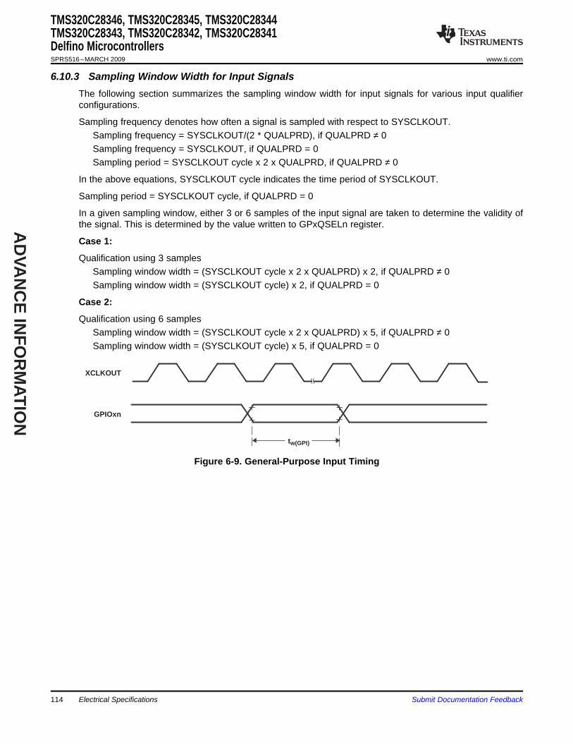
AD
VAN
CE
INF
OR
MA
TIO
N
6.10.3 Sampling Window Width for Input Signals
GPIOxn
XCLKOUT
tw(GPI)
TMS320C28346, TMS320C28345, TMS320C28344TMS320C28343, TMS320C28342, TMS320C28341Delfino MicrocontrollersSPRS516–MARCH 2009 www.ti.com
The following section summarizes the sampling window width for input signals for various input qualifierconfigurations.
Sampling frequency denotes how often a signal is sampled with respect to SYSCLKOUT.Sampling frequency = SYSCLKOUT/(2 * QUALPRD), if QUALPRD ≠ 0Sampling frequency = SYSCLKOUT, if QUALPRD = 0Sampling period = SYSCLKOUT cycle x 2 x QUALPRD, if QUALPRD ≠ 0
In the above equations, SYSCLKOUT cycle indicates the time period of SYSCLKOUT.
Sampling period = SYSCLKOUT cycle, if QUALPRD = 0
In a given sampling window, either 3 or 6 samples of the input signal are taken to determine the validity ofthe signal. This is determined by the value written to GPxQSELn register.
Case 1:
Qualification using 3 samplesSampling window width = (SYSCLKOUT cycle x 2 x QUALPRD) x 2, if QUALPRD ≠ 0Sampling window width = (SYSCLKOUT cycle) x 2, if QUALPRD = 0
Case 2:
Qualification using 6 samplesSampling window width = (SYSCLKOUT cycle x 2 x QUALPRD) x 5, if QUALPRD ≠ 0Sampling window width = (SYSCLKOUT cycle) x 5, if QUALPRD = 0
Figure 6-9. General-Purpose Input Timing
114 Electrical Specifications Submit Documentation Feedback

AD
VAN
CE
INF
OR
MA
TIO
N
6.10.4 Low-Power Mode Wakeup Timing
WAKE INT (A)
XCLKOUT
Address/Data(internal)
td(WAKE−IDLE)
tw(WAKE−INT)
TMS320C28346, TMS320C28345, TMS320C28344TMS320C28343, TMS320C28342, TMS320C28341
Delfino Microcontrollerswww.ti.com SPRS516–MARCH 2009
Table 6-13 shows the timing requirements, Table 6-14 shows the switching characteristics, andFigure 6-10 shows the timing diagram for IDLE mode.
Table 6-13. IDLE Mode Timing Requirements (1)
MIN NOM MAX UNITWithout input qualifier 2tc(SCO)Pulse duration, external wake-uptw(WAKE-INT) cyclessignal With input qualifier 5tc(SCO) + tw(IQSW)
(1) For an explanation of the input qualifier parameters, see Table 6-12.
Table 6-14. IDLE Mode Switching Characteristics (1)
PARAMETER TEST CONDITIONS MIN TYP MAX UNITDelay time, external wake signal toprogram execution resume (2)
td(WAKE-IDLE) Without input qualifier 20tc(SCO) cycles• Wake-up from SARAMWith input qualifier 20tc(SCO) + tw(IQSW)
(1) For an explanation of the input qualifier parameters, see Table 6-12.(2) This is the time taken to begin execution of the instruction that immediately follows the IDLE instruction. execution of an ISR (triggered
by the wake up) signal involves additional latency.
A. WAKE INT can be any enabled interrupt, WDINT, XNMI, or XRS.
Figure 6-10. IDLE Entry and Exit Timing
Table 6-15. STANDBY Mode Timing RequirementsTEST CONDITIONS MIN NOM MAX UNIT
Without input qualification 3tc(OSCCLK)Pulse duration, externaltw(WAKE-INT) cycleswake-up signal With input qualification (1) (2 + QUALSTDBY) * tc(OSCCLK)
(1) QUALSTDBY is a 6-bit field in the LPMCR0 register.
Submit Documentation Feedback Electrical Specifications 115

AD
VAN
CE
INF
OR
MA
TIO
N
tw(WAKE-INT)
td(WAKE-STBY)
td(IDLE−XCOL)
Wake−upSignal
X1/X2 orX1 or
XCLKIN
XCLKOUT
STANDBY Normal ExecutionSTANDBY
Flushing Pipeline
(A)(B)
(C)(D)
(E)(F)
DeviceStatus
TMS320C28346, TMS320C28345, TMS320C28344TMS320C28343, TMS320C28342, TMS320C28341Delfino MicrocontrollersSPRS516–MARCH 2009 www.ti.com
Table 6-16. STANDBY Mode Switching CharacteristicsPARAMETER TEST CONDITIONS MIN TYP MAX UNITDelay time, IDLE instructiontd(IDLE-XCOL) 32tc(SCO) 45tc(SCO) cyclesexecuted to XCLKOUT lowDelay time, external wake
td(WAKE-STBY) signal to program execution cyclesresume (1)
Without input qualifier 100tc(SCO) cycles• Wake up from SARAMWith input qualifier 100tc(SCO) + tw(WAKE-INT)
(1) This is the time taken to begin execution of the instruction that immediately follows the IDLE instruction. execution of an ISR (triggeredby the wake up signal) involves additional latency.
A. IDLE instruction is executed to put the device into STANDBY mode.B. The PLL block responds to the STANDBY signal. SYSCLKOUT is held for the number of cycles indicated below
before being turned off:• 8 cycles, when DIVSEL = 00• 16 cycles, when DIVSEL = 00 or 01• 32 cycles, when DIVSEL = 10• 64 cycles, when DIVSEL = 11
This delay enables the CPU pipeline and any other pending operations to flush properly. If an access to XINTF isin progress and its access time is longer than this number then it will fail. It is recommended to enter STANDBYmode from SARAM without an XINTF access in progress.
C. Clock to the peripherals are turned off. However, the PLL and watchdog are not shut down. The device is now inSTANDBY mode.
D. The external wake-up signal is driven active.E. After a latency period, the STANDBY mode is exited.F. Normal execution resumes. The device will respond to the interrupt (if enabled).
Figure 6-11. STANDBY Entry and Exit Timing Diagram
Table 6-17. HALT Mode Timing RequirementsMIN NOM MAX UNIT
tw(WAKE-GPIO) Pulse duration, GPIO wake-up signal toscst + 2tc(OSCCLK)(1) cycles
tw(WAKE-XRS) Pulse duration, XRS wakeup signal toscst + 8tc(OSCCLK) cycles
(1) See Table 6-10 for an explanation of toscst.
Electrical Specifications116 Submit Documentation Feedback

AD
VAN
CE
INF
OR
MA
TIO
N
td(IDLE−XCOL)
X1/X2
or XCLKIN
XCLKOUT
HALT HALT
Wake-up Latency
Flushing Pipeline
td(WAKE−HALT)
(A)
(B)
(C)
(D)
DeviceStatus
(E) (G)
(F)
PLL Lock-up Time NormalExecution
tw(WAKE-GPIO) tp
GPIOn
Oscillator Start-up Time
TMS320C28346, TMS320C28345, TMS320C28344TMS320C28343, TMS320C28342, TMS320C28341
Delfino Microcontrollerswww.ti.com SPRS516–MARCH 2009
Table 6-18. HALT Mode Switching CharacteristicsPARAMETER MIN TYP MAX UNIT
Delay time, IDLE instruction executed to XCLKOUTtd(IDLE-XCOL) 32tc(SCO) 45tc(SCO) cycleslowtp PLL lock-up time 2600tc(OSCCLK) cycles
Delay time, PLL lock to program execution resumetd(WAKE-HALT) 35tc(SCO) cycles
• Wake up from SARAM
A. IDLE instruction is executed to put the device into HALT mode.B. The PLL block responds to the HALT signal. SYSCLKOUT is held for the number of cycles indicated below before
oscillator is turned off and the CLKIN to the core is stopped:• 8 cycles when DIVSEL = 00• 16 cycles, when DIVSEL = 01• 32 cycles, when DIVSEL = 10• 64 cycles, when DIVSEL = 11This delay enables the CPU pipeline and any other pending operations to flush properly. If an access to XINTF is inprogress and its access time is longer than this number then it will fail. It is recommended to enter HALT mode fromSARAM without an XINTF access in progress.
C. Clocks to the peripherals are turned off and the PLL is shut down. If a quartz crystal or ceramic resonator is used asthe clock source, the internal oscillator is shut down as well. The device is now in HALT mode and consumesabsolute minimum power.
D. When the GPIOn pin (used to bring the device out of HALT) is driven low, the oscillator is turned on and the oscillatorwake-up sequence is initiated. The GPIO pin should be driven high only after the oscillator has stabilized. Thisenables the provision of a clean clock signal during the PLL lock sequence. Since the falling edge of the GPIO pinasynchronously begins the wakeup process, care should be taken to maintain a low noise environment prior toentering and during HALT mode.
E. Once the oscillator has stabilized, the PLL lock sequence is initiated, which takes 131,072 OSCCLK (X1/X2 or X1 orXCLKIN) cycles.
F. Clocks to the core and peripherals are enabled. The HALT mode is now exited. The device will respond to theinterrupt (if enabled), after a latency.
G. Normal operation resumes.
Figure 6-12. HALT Wake-Up Using GPIOn
Submit Documentation Feedback Electrical Specifications 117

AD
VAN
CE
INF
OR
MA
TIO
N
6.11 Enhanced Control Peripherals
6.11.1 Enhanced Pulse Width Modulator (ePWM) Timing
6.11.2 Trip-Zone Input Timing
PWM(B)
TZ
XCLKOUT(A)
tw(TZ)
td(TZ-PWM)HZ
TMS320C28346, TMS320C28345, TMS320C28344TMS320C28343, TMS320C28342, TMS320C28341Delfino MicrocontrollersSPRS516–MARCH 2009 www.ti.com
PWM refers to PWM outputs on ePWM1-6. Table 6-19 shows the PWM timing requirements andTable 6-20, switching characteristics.
Table 6-19. ePWM Timing Requirements (1)
TEST CONDITIONS MIN MAX UNITtw(SYCIN) Sync input pulse width Asynchronous 2tc(SCO) cycles
Synchronous 2tc(SCO) cyclesWith input qualifier 1tc(SCO) + tw(IQSW) cycles
(1) For an explanation of the input qualifier parameters, see Table 6-12.
Table 6-20. ePWM Switching CharacteristicsPARAMETER TEST CONDITIONS MIN MAX UNIT
tw(PWM) Pulse duration, PWMx output high/low 20 nstw(SYNCOUT) Sync output pulse width 8tc(SCO) cyclestd(PWM)tza Delay time, trip input active to PWM forced high no pin load 25 ns
Delay time, trip input active to PWM forced lowtd(TZ-PWM)HZ Delay time, trip input active to PWM Hi-Z 20 ns
A. TZ - TZ1, TZ2, TZ3, TZ4, TZ5, TZ6B. PWM refers to all the PWM pins in the device. The state of the PWM pins after TZ is taken high depends on the PWM
recovery software.
Figure 6-13. PWM Hi-Z Characteristics
Table 6-21. Trip-Zone input Timing Requirements (1)
MIN MAX UNITtw(TZ) Pulse duration, TZx input low Asynchronous 1tc(SCO) cycles
Synchronous 2tc(SCO) cyclesWith input qualifier 1tc(SCO) + tw(IQSW) cycles
(1) For an explanation of the input qualifier parameters, see Table 6-12.
Table 6-22 shows the high-resolution PWM switching characteristics.
Electrical Specifications118 Submit Documentation Feedback

AD
VAN
CE
INF
OR
MA
TIO
N
TMS320C28346, TMS320C28345, TMS320C28344TMS320C28343, TMS320C28342, TMS320C28341
Delfino Microcontrollerswww.ti.com SPRS516–MARCH 2009
Table 6-22. High Resolution PWM Characteristics at SYSCLKOUT = (150 - 300 MHz)MIN TYP MAX UNIT
Micro Edge Positioning (MEP) step size (1) VDD = 1.2 V 55 120 psVDD = 1.1 V 65 140 ps
(1) Maximum MEP step size is based on worst-case process, maximum temperature and maximum voltage. MEP step size will increasewith low voltage and high temperature and decrease with voltage and cold temperature.Applications that use the HRPWM feature should use MEP Scale Factor Optimizer (SFO) estimation software functions. See the TIsoftware libraries for details of using SFO function in end applications. SFO functions help to estimate the number of MEP steps perSYSCLKOUT period dynamically while the HRPWM is in operation.
Table 6-23 shows the eCAP timing requirement and Table 6-24 shows the eCAP switching characteristics.
Table 6-23. Enhanced Capture (eCAP) Timing Requirement (1)
TEST CONDITIONS MIN MAX UNITtw(CAP) Capture input pulse width Asynchronous 2tc(SCO) cycles
Synchronous 2tc(SCO) cyclesWith input qualifier 1tc(SCO) + tw(IQSW) cycles
(1) For an explanation of the input qualifier parameters, see Table 6-12.
Table 6-24. eCAP Switching CharacteristicsPARAMETER TEST CONDITIONS MIN MAX UNIT
tw(APWM) Pulse duration, APWMx output high/low 20 ns
Table 6-25 shows the eQEP timing requirement and Table 6-26 shows the eQEP switchingcharacteristics.
Table 6-25. Enhanced Quadrature Encoder Pulse (eQEP) Timing Requirements (1)
TEST CONDITIONS MIN MAX UNITtw(QEPP) QEP input period Asynchronous/synchronous 2tc(SCO) cycles
With input qualifier 2(1tc(SCO) + tw(IQSW)) cyclestw(INDEXH) QEP Index Input High time Asynchronous/synchronous 2tc(SCO) cycles
With input qualifier 2tc(SCO) +tw(IQSW) cyclestw(INDEXL) QEP Index Input Low time Asynchronous/synchronous 2tc(SCO) cycles
With input qualifier 2tc(SCO) + tw(IQSW) cyclestw(STROBH) QEP Strobe High time Asynchronous/synchronous 2tc(SCO) cycles
With input qualifier 2tc(SCO) + tw(IQSW) cyclestw(STROBL) QEP Strobe Input Low time Asynchronous/synchronous 2tc(SCO) cycles
With input qualifier 2tc(SCO) +tw(IQSW) cycles
(1) For an explanation of the input qualifier parameters, see Table 6-12.
Table 6-26. eQEP Switching CharacteristicsPARAMETER TEST CONDITIONS MIN MAX UNIT
td(CNTR)xin Delay time, external clock to counter increment 4tc(SCO) cyclestd(PCS-OUT)QEP Delay time, QEP input edge to position compare sync 6tc(SCO) cycles
output
Table 6-27. External ADC Start-of-Conversion Switching CharacteristicsPARAMETER MIN MAX UNIT
tw(ADCSOCAL) Pulse duration, ADCSOCAO low 32tc(HCO) cycles
Submit Documentation Feedback Electrical Specifications 119

AD
VAN
CE
INF
OR
MA
TIO
N
ADCSOCAO or
ADCSOCBO
tw(ADCSOCAL)
6.12 External Interrupt Timing
XNMI, XINT1, XINT2
tw(INT)
Interrupt Vector
td(INT)
Address bus (internal)
TMS320C28346, TMS320C28345, TMS320C28344TMS320C28343, TMS320C28342, TMS320C28341Delfino MicrocontrollersSPRS516–MARCH 2009 www.ti.com
Figure 6-14. ADCSOCAO or ADCSOCBO Timing
Figure 6-15. External Interrupt Timing
Table 6-28. External Interrupt Timing Requirements (1)
TEST CONDITIONS MIN MAX UNITtw(INT)
(2) Pulse duration, INT input low/high Synchronous 1tc(SCO) cyclesWith qualifier 1tc(SCO) + tw(IQSW) cycles
(1) For an explanation of the input qualifier parameters, see Table 6-12.(2) This timing is applicable to any GPIO pin configured for ADCSOC functionality.
Table 6-29. External Interrupt Switching Characteristics (1)
PARAMETER MIN MAX UNITtd(INT) Delay time, INT low/high to interrupt-vector fetch tw(IQSW) + 12tc(SCO) cycles
(1) For an explanation of the input qualifier parameters, see Table 6-12.
Electrical Specifications120 Submit Documentation Feedback

AD
VAN
CE
INF
OR
MA
TIO
N
6.13 I2C Electrical Specification and Timing
6.14 Serial Peripheral Interface (SPI) Timing
6.14.1 Master Mode Timing
TMS320C28346, TMS320C28345, TMS320C28344TMS320C28343, TMS320C28342, TMS320C28341
Delfino Microcontrollerswww.ti.com SPRS516–MARCH 2009
Table 6-30. I2C TimingTEST CONDITIONS MIN MAX UNIT
fSCL SCL clock frequency I2C clock module frequency is between 400 kHz7 MHz and 12 MHz and I2C prescaler andclock divider registers are configuredappropriately
vil Low level input voltage 0.3 VDDIO VVih High level input voltage 0.7 VDDIO VVhys Input hysteresis 0.05 VDDIO VVol Low level output voltage 3-mA sink current 0 0.4 VtLOW Low period of SCL clock I2C clock module frequency is between 1.3 µs
7 MHz and 12 MHz and I2C prescaler andclock divider registers are configuredappropriately
tHIGH High period of SCL clock I2C clock module frequency is between 0.6 µs7 MHz and 12 MHz and I2C prescaler andclock divider registers are configuredappropriately
lI Input current with an input voltage -10 10 µAbetween 0.1 VDDIO and 0.9 VDDIO MAX
This section contains both Master Mode and Slave Mode timing data.
Table 6-31 lists the master mode timing (clock phase = 0) and Table 6-32 lists the timing (clockphase = 1). Figure 6-16 and Figure 6-17 show the timing waveforms.
Submit Documentation Feedback Electrical Specifications 121

TMS320C28346, TMS320C28345, TMS320C28344TMS320C28343, TMS320C28342, TMS320C28341Delfino MicrocontrollersSPRS516–MARCH 2009 www.ti.com
Table 6-31. SPI Master Mode External Timing (Clock Phase = 0) (1) (2) (3) (4) (5)
SPI WHEN (SPIBRR + 1) IS EVEN OR SPI WHEN (SPIBRR + 1) IS ODDSPIBRR = 0 OR 2 AND SPIBRR > 3NO. UNIT
MIN MAX MIN MAX1 tc(SPC)M Cycle time, SPICLK 4tc(LCO) 128tc(LCO) 5tc(LCO) 127tc(LCO) ns2 tw(SPCH)M Pulse duration, SPICLK high 0.5tc(SPC)M -10 0.5tc(SPC)M 0.5tc(SPC)M - 0.5tc(LCO) - 10 0.5tc(SPC)M - 0.5tc(LCO) ns
(clock polarity = 0)tw(SPCL)M Pulse duration, SPICLK low 0.5tc(SPC)M - 10 0.5tc(SPC)M 0.5tc(SPC)M - 0.5tc(LCO) - 10 0.5tc(SPC)M - 0.5tc(LCO)
(clock polarity = 1)3 tw(SPCL)M Pulse duration, SPICLK low 0.5tc(SPC)M - 10 0.5tc(SPC)M 0.5tc(SPC)M + 0.5tc(LCO)-10 0.5tc(SPC)M + 0.5tc(LCO) ns
(clock polarity = 0)tw(SPCH)M Pulse duration, SPICLK high 0.5tc(SPC)M - 10 0.5tc(SPC)M 0.5tc(SPC)M + 0.5tc(LCO)- 10 0.5tc(SPC)M + 0.5tc(LCO)
(clock polarity = 1)4 td(SPCH-SIMO)M Delay time, SPICLK high to SPISIMO 10 10 ns
valid (clock polarity = 0)td(SPCL-SIMO)M Delay time, SPICLK low to SPISIMO 10 10
valid (clock polarity = 1)5 tv(SPCL-SIMO)M Valid time, SPISIMO data valid after 0.5tc(SPC)M -10 0.5tc(SPC)M + 0.5tc(LCO) -10
SPICLK low (clock polarity = 0)tv(SPCH-SIMO)M Valid time, SPISIMO data valid after 0.5tc(SPC)M -10 0.5tc(SPC)M + 0.5tc(LCO) -10
SPICLK high (clock polarity = 1)8 tsu(SOMI-SPCL)M Setup time, SPISOMI before SPICLK 20 20 ns
low (clock polarity = 0)tsu(SOMI-SPCH)M Setup time, SPISOMI before SPICLK 20 20 ns
high (clock polarity = 1)9 tv(SPCL-SOMI)M Valid time, SPISOMI data valid after 0.25tc(SPC)M -10 0.5tc(SPC)M- 0.5tc(LCO)- 10
SPICLK low (clock polarity = 0)tv(SPCH-SOMI)M Valid time, SPISOMI data valid after 0.25tc(SPC)M - 10 0.5tc(SPC)M- 0.5tc(LCO)- 10 ns
SPICLK high (clock polarity = 1)
(1) The MASTER / SLAVE bit (SPICTL.2) is set and the CLOCK PHASE bit (SPICTL.3) is cleared.(2) tc(SPC) = SPI clock cycle time = LSPCLK/4 or LSPCLK/(SPIBRR +1)(3) tc(LCO) = LSPCLK cycle time(4) Internal clock prescalers must be adjusted such that the SPI clock speed is limited to the following SPI clock rate:
Master mode transmit 25-MHz MAX, master mode receive 12.5-MHz MAXSlave mode transmit 20-MHz MAX, slave mode receive 20-MHz MAX.
(5) The active edge of the SPICLK signal referenced is controlled by the clock polarity bit (SPICCR.6).
122 Electrical Specifications Submit Documentation Feedback

AD
VAN
CE
INF
OR
MA
TIO
N
9
4
SPISOMI
SPISIMO
SPICLK (clock polarity = 1)
SPICLK (clock polarity = 0)
Master In DataMust Be Valid
Master Out Data Is Valid
8
5
3
2
1
SPISTE(A)
TMS320C28346, TMS320C28345, TMS320C28344TMS320C28343, TMS320C28342, TMS320C28341
Delfino Microcontrollerswww.ti.com SPRS516–MARCH 2009
A. In the master mode, SPISTE goes active 1tc(SPC) (minimum) before valid SPI clock edge. On the trailing end of theword, the SPISTE will go inactive 1tc(SPC) after the receiving edge (SPICLK) of the last data bit, except that SPISTEstays active between back-to-back transmit words in both FIFO and nonFIFO modes.
Figure 6-16. SPI Master Mode External Timing (Clock Phase = 0)
Submit Documentation Feedback Electrical Specifications 123

TMS320C28346, TMS320C28345, TMS320C28344TMS320C28343, TMS320C28342, TMS320C28341Delfino MicrocontrollersSPRS516–MARCH 2009 www.ti.com
Table 6-32. SPI Master Mode External Timing (Clock Phase = 1) (1) (2) (3) (4) (5)
SPI WHEN (SPIBRR + 1) IS EVEN OR SPI WHEN (SPIBRR + 1) IS ODDSPIBRR = 0 AND SPIBRR > 3
NO. UNITOR 2MIN MAX MIN MAX
1 tc(SPC)M Cycle time, SPICLK 4tc(LCO) 128tc(LCO) 5tc(LCO) 127tc(LCO) ns2 tw(SPCH)M Pulse duration, SPICLK high (clock 0.5tc(SPC)M -10 0.5tc(SPC)M 0.5tc(SPC)M - 0.5tc 0.5tc(SPC)M - 0.5tc(LCO) ns
polarity = 0) (LCO)-10tw(SPCL))M Pulse duration, SPICLK low (clock polarity 0.5tc(SPC)M -10 0.5tc(SPC)M 0.5tc(SPC)M - 0.5tc 0.5tc(SPC)M - 0.5tc(LCO ns
= 1) (LCO)-103 tw(SPCL)M Pulse duration, SPICLK low (clock polarity 0.5tc(SPC)M -10 0.5tc(SPC)M 0.5tc(SPC)M + 0.5tc(LCO) - 0.5tc(SPC)M + 0.5tc(LCO) ns
= 0) 10tw(SPCH)M Pulse duration, SPICLK high (clock 0.5tc(SPC)M -10 0.5tc(SPC)M 0.5tc(SPC)M + 0.5tc(LCO) 0.5tc(SPC)M + 0.5tc(LCO) ns
polarity = 1) -106 tsu(SIMO-SPCH)M Setup time, SPISIMO data valid before 0.5tc(SPC)M -10 0.5tc(SPC)M - 10 ns
SPICLK high (clock polarity = 0)tsu(SIMO-SPCL)M Setup time, SPISIMO data valid before 0.5tc(SPC)M -10 0.5tc(SPC)M - 10 ns
SPICLK low (clock polarity = 1)7 tv(SPCH-SIMO)M Valid time, SPISIMO data valid after 0.5tc(SPC)M -10 0.5tc(SPC)M - 10 ns
SPICLK high (clock polarity = 0)tv(SPCL-SIMO)M Valid time, SPISIMO data valid after 0.5tc(SPC)M -10 0.5tc(SPC)M -10 ns
SPICLK low (clock polarity = 1)10 tsu(SOMI-SPCH)M Setup time, SPISOMI before SPICLK high 20 20 ns
(clock polarity = 0)tsu(SOMI-SPCL)M Setup time, SPISOMI before SPICLK low 20 20 ns
(clock polarity = 1)11 tv(SPCH-SOMI)M Valid time, SPISOMI data valid after 0.25tc(SPC)M -10 0.5tc(SPC)M -10 ns
SPICLK high (clock polarity = 0)tv(SPCL-SOMI)M Valid time, SPISOMI data valid after 0.25tc(SPC)M -10 0.5tc(SPC)M -10 ns
SPICLK low (clock polarity = 1)
(1) The MASTER/SLAVE bit (SPICTL.2) is set and the CLOCK PHASE bit (SPICTL.3) is set.(2) tc(SPC) = SPI clock cycle time = LSPCLK/4 or LSPCLK/(SPIBRR + 1)(3) Internal clock prescalers must be adjusted such that the SPI clock speed is limited to the following SPI clock rate:
Master mode transmit 25-MHz MAX, master mode receive 12.5 MHz MAXSlave mode transmit 20-MHz MAX, slave mode receive 20 MHz MAX.
(4) tc(LCO) = LSPCLK cycle time(5) The active edge of the SPICLK signal referenced is controlled by the CLOCK POLARITY bit (SPICCR.6).
124 Electrical Specifications Submit Documentation Feedback

AD
VAN
CE
INF
OR
MA
TIO
N
Data Valid
11
SPISOMI
SPISIMO
SPICLK (clock polarity = 1)
SPICLK (clock polarity = 0)
Master In Data MustBe Valid
Master Out Data Is Valid
1
7
6
10
3
2
SPISTE(A)
6.14.2 SPI Slave Mode Timing
TMS320C28346, TMS320C28345, TMS320C28344TMS320C28343, TMS320C28342, TMS320C28341
Delfino Microcontrollerswww.ti.com SPRS516–MARCH 2009
A. In the master mode, SPISTE goes active 1tc(SPC) (minimum) before valid SPI clock edge. On the trailing end of theword, the SPISTE will go inactive 1tc(SPC) after the receiving edge (SPICLK) of the last data bit, except that SPISTEstays active between back-to-back transmit words in both FIFO and nonFIFO modes.
Figure 6-17. SPI Master Mode External Timing (Clock Phase = 1)
Table 6-33 lists the slave mode external timing (clock phase = 0) and Table 6-34 (clock phase = 1).Figure 6-18 and Figure 6-19 show the timing waveforms.
Table 6-33. SPI Slave Mode External Timing (Clock Phase = 0) (1) (2) (3) (4) (5)
NO. MIN MAX UNIT12 tc(SPC)S Cycle time, SPICLK 4tc(LCO) ns13 tw(SPCH)S Pulse duration, SPICLK high (clock polarity = 0) 0.5tc(SPC)S - 10 0.5tc(SPC)S ns
tw(SPCL)S Pulse duration, SPICLK low (clock polarity = 1) 0.5tc(SPC)S - 10 0.5tc(SPC)S ns14 tw(SPCL)S Pulse duration, SPICLK low (clock polarity = 0) 0.5tc(SPC)S - 10 0.5tc(SPC)S ns
tw(SPCH)S Pulse duration, SPICLK high (clock polarity = 1) 0.5tc(SPC)S - 10 0.5tc(SPC)S ns15 td(SPCH-SOMI)S Delay time, SPICLK high to SPISOMI valid (clock polarity = 0) 20 ns
td(SPCL-SOMI)S Delay time, SPICLK low to SPISOMI valid (clock polarity = 1) 20 ns16 tv(SPCL-SOMI)S Valid time, SPISOMI data valid after SPICLK low 0.75tc(SPC)S ns
(clock polarity = 0)tv(SPCH-SOMI)S Valid time, SPISOMI data valid after SPICLK high 0.75tc(SPC)S ns
(clock polarity = 1)
(1) The MASTER / SLAVE bit (SPICTL.2) is cleared and the CLOCK PHASE bit (SPICTL.3) is cleared.(2) tc(SPC) = SPI clock cycle time = LSPCLK/4 or LSPCLK/(SPIBRR + 1)(3) Internal clock prescalers must be adjusted such that the SPI clock speed is limited to the following SPI clock rate:
Master mode transmit 25-MHz MAX, master mode receive 12.5-MHz MAXSlave mode transmit 20-MHz MAX, slave mode receive 20-MHz MAX.
(4) tc(LCO) = LSPCLK cycle time(5) The active edge of the SPICLK signal referenced is controlled by the CLOCK POLARITY bit (SPICCR.6).
Submit Documentation Feedback Electrical Specifications 125

AD
VAN
CE
INF
OR
MA
TIO
N
20
15
SPISIMO
SPISOMI
SPICLK(clock polarity = 1)
SPICLK(clock polarity = 0)
SPISIMO DataMust Be Valid
SPISOMI Data Is Valid
19
16
14
13
12
SPISTE(A)
TMS320C28346, TMS320C28345, TMS320C28344TMS320C28343, TMS320C28342, TMS320C28341Delfino MicrocontrollersSPRS516–MARCH 2009 www.ti.com
Table 6-33. SPI Slave Mode External Timing (Clock Phase = 0) (continued)NO. MIN MAX UNIT19 tsu(SIMO-SPCL)S Setup time, SPISIMO before SPICLK low (clock polarity = 0) 20 ns
tsu(SIMO-SPCH)S Setup time, SPISIMO before SPICLK high (clock polarity = 1) 20 ns20 tv(SPCL-SIMO)S Valid time, SPISIMO data valid after SPICLK low 0.5tc(SPC)S-10 ns
(clock polarity = 0)tv(SPCH-SIMO)S Valid time, SPISIMO data valid after SPICLK high 0.5tc(SPC)S-10 ns
(clock polarity = 1)
A. In the slave mode, the SPISTE signal should be asserted low at least 1tc(SPC) (minimum) before the valid SPI clockedge and remain low for at least 1tc(SPC) after the receiving edge (SPICLK) of the last data bit.
Figure 6-18. SPI Slave Mode External Timing (Clock Phase = 0)
Table 6-34. SPI Slave Mode External Timing (Clock Phase = 1) (1) (2) (3) (4)
NO. MIN MAX UNIT12 tc(SPC)S Cycle time, SPICLK 8tc(LCO) ns13 tw(SPCH)S Pulse duration, SPICLK high (clock polarity = 0) 0.5tc(SPC)S - 10 0.5tc(SPC)S ns
tw(SPCL)S Pulse duration, SPICLK low (clock polarity = 1) 0.5tc(SPC)S - 10 0.5tc(SPC)S ns14 tw(SPCL)S Pulse duration, SPICLK low (clock polarity = 0) 0.5tc(SPC)S - 10 0.5tc(SPC)S ns
tw(SPCH)S Pulse duration, SPICLK high (clock polarity = 1) 0.5tc(SPC)S - 10 0.5tc(SPC)S ns17 tsu(SOMI-SPCH)S Setup time, SPISOMI before SPICLK high (clock polarity = 0) 0.125tc(SPC)S ns
tsu(SOMI-SPCL)S Setup time, SPISOMI before SPICLK low (clock polarity = 1) 0.125tc(SPC)S ns
(1) The MASTER / SLAVE bit (SPICTL.2) is cleared and the CLOCK PHASE bit (SPICTL.3) is cleared.(2) tc(SPC) = SPI clock cycle time = LSPCLK/4 or LSPCLK/(SPIBRR + 1)(3) Internal clock prescalers must be adjusted such that the SPI clock speed is limited to the following SPI clock rate:
Master mode transmit 25-MHz MAX, master mode receive 12.5-MHz MAXSlave mode transmit 20-MHz MAX, slave mode receive 20-MHz MAX.
(4) The active edge of the SPICLK signal referenced is controlled by the CLOCK POLARITY bit (SPICCR.6).
126 Electrical Specifications Submit Documentation Feedback

AD
VAN
CE
INF
OR
MA
TIO
N
Data Valid
22
SPISIMO
SPISOMI
SPICLK(clock polarity = 1)
SPICLK(clock polarity = 0)
SPISIMO DataMust Be Valid
SPISOMI Data Is Valid
21
12
18
17
14
13
SPISTE(A)
6.15 External Interface (XINTF) Timing
TMS320C28346, TMS320C28345, TMS320C28344TMS320C28343, TMS320C28342, TMS320C28341
Delfino Microcontrollerswww.ti.com SPRS516–MARCH 2009
Table 6-34. SPI Slave Mode External Timing (Clock Phase = 1) (continued)NO. MIN MAX UNIT18 tv(SPCH-SOMI)S Valid time, SPISOMI data valid after SPICLK low 0.75tc(SPC)S ns
(clock polarity = 0)tv(SPCL-SOMI)S Valid time, SPISOMI data valid after SPICLK high 0.75tc(SPC)S ns
(clock polarity = 1)21 tsu(SIMO-SPCH)S Setup time, SPISIMO before SPICLK high (clock polarity = 0) 20 ns
tsu(SIMO-SPCL)S Setup time, SPISIMO before SPICLK low (clock polarity = 1) 20 ns22 tv(SPCH-SIMO)S Valid time, SPISIMO data valid after SPICLK high 0.5tc(SPC)S-10 ns
(clock polarity = 0)tv(SPCL-SIMO)S Valid time, SPISIMO data valid after SPICLK low 0.5tc(SPC)S-10 ns
(clock polarity = 1)
A. In the slave mode, the SPISTE signal should be asserted low at least 1tc(SPC) before the valid SPI clock edge andremain low for at least 1tc(SPC) after the receiving edge (SPICLK) of the last data bit.
Figure 6-19. SPI Slave Mode External Timing (Clock Phase = 1)
Each XINTF access consists of three parts: Lead, Active, and Trail. The user configures theLead/Active/Trail wait states in the XTIMING registers. There is one XTIMING register for each XINTFzone. Table 6-35 shows the relationship between the parameters configured in the XTIMING register andthe duration of the pulse in terms of XTIMCLK cycles.
Table 6-35. Relationship Between Parameters Configured in XTIMING and Duration of PulseDURATION (ns) (1) (2)
DESCRIPTIONX2TIMING = 0 X2TIMING = 1
LR Lead period, read access XRDLEAD × tc(XTIM) (XRDLEAD × 2) × tc(XTIM)
(1) tc(XTIM) – Cycle time, XTIMCLK(2) WS refers to the number of wait states inserted by hardware when using XREADY. If the zone is configured to ignore XREADY
(USEREADY = 0), then WS = 0.
Submit Documentation Feedback Electrical Specifications 127

AD
VAN
CE
INF
OR
MA
TIO
N
6.15.1 USEREADY = 0
6.15.2 Synchronous Mode (USEREADY = 1, READYMODE = 0)
TMS320C28346, TMS320C28345, TMS320C28344TMS320C28343, TMS320C28342, TMS320C28341Delfino MicrocontrollersSPRS516–MARCH 2009 www.ti.com
Table 6-35. Relationship Between Parameters Configured in XTIMING and Duration of Pulse (continued)DURATION (ns) (1) (2)
DESCRIPTIONX2TIMING = 0 X2TIMING = 1
AR Active period, read access (XRDACTIVE + WS + 1) × tc(XTIM) (XRDACTIVE × 2 + WS + 1) × tc(XTIM)
TR Trail period, read access XRDTRAIL × tc(XTIM) (XRDTRAIL × 2) × tc(XTIM)
LW Lead period, write access XWRLEAD × tc(XTIM) (XWRLEAD × 2) × tc(XTIM)
AW Active period, write access (XWRACTIVE + WS + 1) × tc(XTIM) (XWRACTIVE × 2 + WS + 1) × tc(XTIM)
TW Trail period, write access XWRTRAIL × tc(XTIM) (XWRTRAIL × 2) × tc(XTIM)
Minimum wait state requirements must be met when configuring each zone’s XTIMING register. Theserequirements are in addition to any timing requirements as specified by that device’s data sheet. Nointernal device hardware is included to detect illegal settings.
If the XREADY signal is ignored (USEREADY = 0), then:
Lead: LR ≥ 2 × tc(XTIM)
LW ≥ 3 × tc(XTIM)
Active: AR ≥ 6 × tc(XTIM)
AW ≥ 1 × tc(XTIM)
Trail: TW ≥ 3 × tc(XTIM)
These requirements result in the following XTIMING register configuration restrictions:XRDLEAD XRDACTIVE XRDTRAIL XWRLEAD XWRACTIVE XWRTRAIL X2TIMING
≥ 2 ≥ 6 ≥ 0 ≥ 3 ≥ 1 ≥ 3 0 (1)
(1) If X2TIMCLK is enabled, specified Lead, Active, and Trail restrictions can be divided by 2 for values with even numbers.
Examples of valid and invalid timing when not sampling XREADY:XRDLEAD XRDACTIVE XRDTRAIL XWRLEAD XWRACTIVE XWRTRAIL X2TIMING
Invalid (1) 0 0 0 0 0 0 0, 1Valid (2) 2 6 0 3 1 3 0 (3)
(1) No hardware to detect illegal XTIMING configurations(2) Based on 300-MHz system clock speed.(3) If X2TIMCLK is enabled, specified Lead, Active, and Trail restrictions can be divided by 2 for values with even numbers.
If the XREADY signal is sampled in the synchronous mode (USEREADY = 1, READYMODE = 0), then:
1 Lead: LR ≥ × 2 t c(XTIM)
LW ≥ 3 × tc(XTIM)
2 Active: AR ≥ 6 × tc(XTIM)
AW ≥ 2 × tc(XTIM)
3 Trail: TW ≥ 3 × tc(XTIM)
NOTERestriction does not include external hardware wait states.
These requirements result in the following XTIMING register configuration restrictions (based on 300-MHzsystem clock speed):
Electrical Specifications128 Submit Documentation Feedback

AD
VAN
CE
INF
OR
MA
TIO
N
6.15.3 Asynchronous Mode (USEREADY = 1, READYMODE = 1)
TMS320C28346, TMS320C28345, TMS320C28344TMS320C28343, TMS320C28342, TMS320C28341
Delfino Microcontrollerswww.ti.com SPRS516–MARCH 2009
XRDLEAD XRDACTIVE XRDTRAIL XWRLEAD XWRACTIVE XWRTRAIL X2TIMING≥ 2 ≥ 6 ≥ 0 ≥ 3 ≥ 2 ≥ 3 0 (1)
(1) If X2TIMCLK is enabled, specified Lead, Active, and Trail restrictions can be divided by 2 for values with even numbers.
Examples of valid and invalid timing when using synchronous XREADY:XRDLEAD XRDACTIVE XRDTRAIL XWRLEAD XWRACTIVE XWRTRAIL X2TIMING
Invalid (1) 0 0 0 0 0 0 0, 1Invalid (1) 1 0 0 1 0 0 0, 1Valid (2) 2 6 0 3 2 3 0 (3)
(1) No hardware to detect illegal XTIMING configurations(2) Based on 300-MHz system clock speed(3) If X2TIMCLK is enabled, specified Lead, Active, and Trail restrictions can be divided by 2 for values with even numbers.
If the XREADY signal is sampled in the asynchronous mode (USEREADY = 1, READYMODE = 1), then:
1 Lead: LR ≥ 2 × tc(XTIM)
LW ≥ 3 × tc(XTIM)
2 Active: AR ≥ 6 × tc(XTIM)
AW ≥ 4 × tc(XTIM)
3 Trail: TW ≥ 3 × tc(XTIM)
NOTERestrictions do not include external hardware wait states.
These requirements result in the following XTIMING register configuration restrictions (based on 300-MHzsystem clock speed):
XRDLEAD XRDACTIVE XRDTRAIL XWRLEAD XWRACTIVE XWRTRAIL X2TIMING≥ 2 ≥ 6 0 ≥ 3 ≥ 4 0 0 (1)
(1) If X2TIMCLK is enabled, specified Lead, Active, and Trail restrictions can be divided by 2 for values with even numbers.
Examples of valid and invalid timing when using asynchronous XREADY:XRDLEAD XRDACTIVE XRDTRAIL XWRLEAD XWRACTIVE XWRTRAIL X2TIMING
Invalid (1) 0 0 0 0 0 0 0, 1Invalid (1) 1 0 0 1 0 0 0, 1Invalid (1) 1 1 0 1 1 0 0Valid (2) 2 6 0 3 4 3 0 (3)
(1) No hardware to detect illegal XTIMING configurations(2) Based on 300-MHz system clock speed(3) If X2TIMCLK is enabled, specified Lead, Active, and Trail restrictions can be divided by 2 for values with even numbers
Unless otherwise specified, all XINTF timing is applicable for the clock configurations shown in Table 6-36.
Submit Documentation Feedback Electrical Specifications 129

AD
VAN
CE
INF
OR
MA
TIO
N
1
0
/2SYSCLKOUT
C28x
CPU
XINTCNF2 (XTIMCLK)
1
0
/2XTIMCLK
XINTCNF2
(CLKMODE)
0
1
0
XTIMING0
XTIMING6
XTIMING7
XBANK
LEAD/ACTIVE/TRAIL
PCLKR3[XINTFENCLK]
XINTCNF2
(CLKOFF)
XCLKOUT1
0
/2
XINTCNF2
(BY4CLKMODE)
6.15.4 XINTF Signal Alignment to XCLKOUT
TMS320C28346, TMS320C28345, TMS320C28344TMS320C28343, TMS320C28342, TMS320C28341Delfino MicrocontrollersSPRS516–MARCH 2009 www.ti.com
Table 6-36. XINTF Clock ConfigurationsMODE SYSCLKOUT XTIMCLK XCLKOUT (1)
1 SYSCLKOUT SYSCLKOUTExample: 300 MHz 300 MHz 300 MHz
2 SYSCLKOUT 1/2 SYSCLKOUTExample: 300 MHz 300 MHz 150 MHz
3 SYSCLKOUT 1/2 SYSCLKOUTExample: 300 MHz 300 MHz 150 MHz
4 SYSCLKOUT 1/4 SYSCLKOUTExample: 300 MHz 300 MHz 75 MHz
5 1/2 SYSCLKOUT 1/2 SYSCLKOUTExample: 300 MHz 150 MHz 150 MHz
6 1/2 SYSCLKOUT 1/4 SYSCLKOUTExample: 300 MHz 150 MHz 75 MHz
7 1/2 SYSCLKOUT 1/4 SYSCLKOUTExample: 300 MHz 150 MHz 75 MHz
8 1/2 SYSCLKOUT 1/8 SYSCLKOUTExample: 300 MHz 150 MHz 37.5 MHz
(1) The XCLKOUT signal is limited to the output buffer speed.
The relationship between SYSCLKOUT and XTIMCLK is shown in Figure 6-20.
Figure 6-20. Relationship Between XTIMCLK and SYSCLKOUT
For each XINTF access, the number of lead, active, and trail cycles is based on the internal clockXTIMCLK. Strobes such as XRD, XWE0, XWE1, and zone chip-select (XZCS) change state in relationshipto the rising edge of XTIMCLK. The external clock, XCLKOUT, can be configured to be either equal to orone-half the frequency of XTIMCLK.
For the case where XCLKOUT = XTIMCLK, all of the XINTF strobes will change state with respect to the
Electrical Specifications130 Submit Documentation Feedback

AD
VAN
CE
INF
OR
MA
TIO
N
6.15.5 External Interface Read Timing
TMS320C28346, TMS320C28345, TMS320C28344TMS320C28343, TMS320C28342, TMS320C28341
Delfino Microcontrollerswww.ti.com SPRS516–MARCH 2009
rising edge of XCLKOUT. For the case where XCLKOUT = one-half or one-fourth XTIMCLK, some strobeswill change state either on the rising edge of XCLKOUT or the falling edge of XCLKOUT. In the XINTFtiming tables, the notation XCOHL is used to indicate that the parameter is with respect to either case;XCLKOUT rising edge (high) or XCLKOUT falling edge (low). If the parameter is always with respect tothe rising edge of XCLKOUT, the notation XCOH is used.
For the case where XCLKOUT = one-half or one-fourth XTIMCLK, the XCLKOUT edge with which thechange will be aligned can be determined based on the number of XTIMCLK cycles from the start of theaccess to the point at which the signal changes. If this number of XTIMCLK cycles is even, the alignmentwill be with respect to the rising edge of XCLKOUT. If this number is odd, then the signal will change withrespect to the falling edge of XCLKOUT. Examples include the following:• Strobes that change at the beginning of an access always align to the rising edge of XCLKOUT. This is
because all XINTF accesses begin with respect to the rising edge of XCLKOUT.
Examples: XZCSL Zone chip-select active lowXRNWL XR/W active low
• Strobes that change at the beginning of the active period will align to the rising edge of XCLKOUT ifthe total number of lead XTIMCLK cycles for the access is even. If the number of lead XTIMCLKcycles is odd, then the alignment will be with respect to the falling edge of XCLKOUT.
Examples: XRDL XRD active lowXWEL XWE1 or XWE0 active low
• Strobes that change at the beginning of the trail period will align to the rising edge of XCLKOUT if thetotal number of lead + active XTIMCLK cycles (including hardware waitstates) for the access is even. Ifthe number of lead + active XTIMCLK cycles (including hardware waitstates) is odd, then the alignmentwill be with respect to the falling edge of XCLKOUT.
Examples: XRDH XRD inactive highXWEH XWE1 or XWE0 inactive high
• Strobes that change at the end of the access will align to the rising edge of XCLKOUT if the totalnumber of lead + active + trail XTIMCLK cycles (including hardware waitstates) is even. If the numberof lead + active + trail XTIMCLK cycles (including hardware waitstates) is odd, then the alignment willbe with respect to the falling edge of XCLKOUT.
Examples: XZCSH Zone chip-select inactive highXRNWH XR/W inactive high
Table 6-37. External Interface Read Timing RequirementsMIN MAX UNIT
ta(A) Access time, read data from address valid (LR + AR) –13.5 (1) nsta(XRD) Access time, read data valid from XRD active low AR –13 (1) nstsu(XD)XRD Setup time, read data valid before XRD strobe inactive high 13 nsth(XD)XRD Hold time, read data valid after XRD inactive high 0 ns
(1) LR = Lead period, read access. AR = Active period, read access. See Table 6-35.
Table 6-38. External Interface Read Switching CharacteristicsPARAMETER MIN MAX UNIT
td(XCOH-XZCSL) Delay time, XCLKOUT high to zone chip-select active low 0 2 nstd(XCOHL-XZCSH) Delay time, XCLKOUT high/low to zone chip-select inactive high –0.2 0.9 ns
Submit Documentation Feedback Electrical Specifications 131
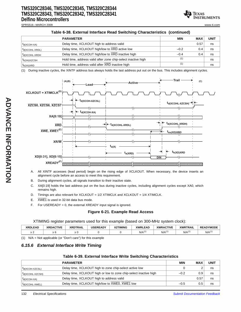
AD
VAN
CE
INF
OR
MA
TIO
N
DIN
td(XCOHL-XRDL)
td(XCOH-XA)
td(XCOH-XZCSL)
td(XCOHL-XRDH)
th(XD)XRD
td(XCOHL-XZCSH)XZCS0 XZCS6 XZCS7, ,
XA[0:19]
XRD
,XWE XWE1(E)
XR/W
XD[0:31], XD[0:15]
tsu(XD)XRD
ta(A)
ta(XRD)
XREADY(F)
LeadActive
Trail
X OUT = XTIMCLK(D)
CLK
(A)(B) (C)
6.15.6 External Interface Write Timing
TMS320C28346, TMS320C28345, TMS320C28344TMS320C28343, TMS320C28342, TMS320C28341Delfino MicrocontrollersSPRS516–MARCH 2009 www.ti.com
Table 6-38. External Interface Read Switching Characteristics (continued)PARAMETER MIN MAX UNIT
td(XCOH-XA) Delay time, XCLKOUT high to address valid 0.57 nstd(XCOHL-XRDL) Delay time, XCLKOUT high/low to XRD active low –0.2 0.4 nstd(XCOHL-XRDH Delay time, XCLKOUT high/low to XRD inactive high –0.4 0.4 nsth(XA)XZCSH Hold time, address valid after zone chip-select inactive high (1) nsth(XA)XRD Hold time, address valid after XRD inactive high (1) ns
(1) During inactive cycles, the XINTF address bus always holds the last address put out on the bus. This includes alignment cycles.
A. All XINTF accesses (lead period) begin on the rising edge of XCLKOUT. When necessary, the device inserts analignment cycle before an access to meet this requirement.
B. During alignment cycles, all signals transition to their inactive state.C. XA[0:19] holds the last address put on the bus during inactive cycles, including alignment cycles except XA0, which
remains high.D. Timings are also relevant for XCLKOUT = 1/2 XTIMCLK and XCLKOUT = 1/4 XTIMCLK.E. XWE1 is used in 32-bit data bus mode.F. For USEREADY = 0, the external XREADY input signal is ignored.
Figure 6-21. Example Read Access
XTIMING register parameters used for this example (based on 300-MHz system clock):XRDLEAD XRDACTIVE XRDTRAIL USEREADY X2TIMING XWRLEAD XWRACTIVE XWRTRAIL READYMODE
≥ 2 ≥ 6 ≥ 0 0 0 N/A (1) N/A (1) N/A (1) N/A (1)
(1) N/A = Not applicable (or “Don’t care”) for this example
Table 6-39. External Interface Write Switching CharacteristicsPARAMETER MIN MAX UNIT
td(XCOH-XZCSL) Delay time, XCLKOUT high to zone chip-select active low 0 2 nstd(XCOHL-XZCSH) Delay time, XCLKOUT high or low to zone chip-select inactive high –0.2 0.9 nstd(XCOH-XA) Delay time, XCLKOUT high to address valid 0.57 nstd(XCOHL-XWEL) Delay time, XCLKOUT high/low to XWE0, XWE1 low –0.5 0.5 ns
Electrical Specifications132 Submit Documentation Feedback

AD
VAN
CE
INF
OR
MA
TIO
N
LeadActive
Trail
td(XCOH-XZCSL)
td(XCOH-XA)
td(XCOHL-XWEL) td(XCOHL-XWEH)
td(XCOHL-XZCSH)
ten(XD)XWEL th(XD)XWEH
tdis(XD)XRNW
XD[0:31], XD[0:15]
XZCS0 XZCS6 XZCS7, ,
td(XCOH-XRNWL)td(XCOHL-XRNWH)
DOUT
XREADY(F)
XR/W
XRD
XCLKOUT = XTIMCLK(D)
XWE0 XWE1,(E)
td(XWEL-XD)
XA[0:19]
(A) (B) (C)
TMS320C28346, TMS320C28345, TMS320C28344TMS320C28343, TMS320C28342, TMS320C28341
Delfino Microcontrollerswww.ti.com SPRS516–MARCH 2009
Table 6-39. External Interface Write Switching Characteristics (continued)PARAMETER MIN MAX UNIT
td(XCOHL-XWEH) Delay time, XCLKOUT high/low to XWE0, XWE1 high –0.5 0.5 nstd(XCOH-XRNWL) Delay time, XCLKOUT high to XR/W low -0.2 0.4 nstd(XCOHL-XRNWH) Delay time, XCLKOUT high/low to XR/W high 0.3 0.6 nsten(XD)XWEL Enable time, data bus driven from XWE0, XWE1 low –7.5 nstd(XWEL-XD) Delay time, data valid after XWE0, XWE1 active low 4 nsth(XA)XZCSH Hold time, address valid after zone chip-select inactive high (1) nsth(XD)XWE Hold time, write data valid after XWE0, XWE1 inactive high TW-7.5 (2) nstdis(XD)XRNW Maximum time for processor to release the data bus after XR/W inactive 0 ns
high
(1) During inactive cycles, the XINTF address bus will always hold the last address put out on the bus except XA0, which remains high.This includes alignment cycles.
(2) TW = Trail period, write access. See Table 6-35.
A. All XINTF accesses (lead period) begin on the rising edge of XCLKOUT. When necessary, the device inserts analignment cycle before an access to meet this requirement.
B. During alignment cycles, all signals transition to their inactive state.C. XA[0:19] holds the last address put on the bus during inactive cycles, including alignment cycles except XA0, which
remains high.D. Timings are also relevant for XCLKOUT = 1/2 XTIMCLK and XCLKOUT = 1/4 XTIMCLK.E. XWE1 is used in 32-bit data bus mode.F. For USEREADY = 0, the external XREADY input signal is ignored.
Figure 6-22. Example Write Access
XTIMING register parameters used for this example (based on 300-MHz system clock):XRDLEAD XRDACTIVE XRDTRAIL USEREADY X2TIMING XWRLEAD XWRACTIVE XWRTRAIL READYMODE
N/A (1) N/A (1) N/A (1) 0 0 ≥ 3 ≥ 1 ≥ 3 N/A (1)
(1) N/A = Not applicable (or “Don’t care”) for this example
Submit Documentation Feedback Electrical Specifications 133

AD
VAN
CE
INF
OR
MA
TIO
N
6.15.7 External Interface Ready-on-Read Timing With One External Wait State
TMS320C28346, TMS320C28345, TMS320C28344TMS320C28343, TMS320C28342, TMS320C28341Delfino MicrocontrollersSPRS516–MARCH 2009 www.ti.com
Table 6-40. External Interface Read Switching Characteristics (Ready-on-Read, 1 Wait State)PARAMETER MIN MAX UNIT
td(XCOH-XZCSL) Delay time, XCLKOUT high to zone chip-select active low 0 2 nstd(XCOHL-XZCSH) Delay time, XCLKOUT high/low to zone chip-select inactive - 0.2 0.9 ns
hightd(XCOH-XA) Delay time, XCLKOUT high to address valid 0.57 nstd(XCOHL-XRDL) Delay time, XCLKOUT high/low to XRD active low –0.2 0.4 nstd(XCOHL-XRDH) Delay time, XCLKOUT high/low to XRD inactive high -0.4 0.4 nsth(XA)XZCSH Hold time, address valid after zone chip-select inactive high (1) nsth(XA)XRD Hold time, address valid after XRD inactive high (1) ns
(1) During inactive cycles, the XINTF address bus always holds the last address put out on the bus. This includes alignment cycles.
Table 6-41. External Interface Read Timing Requirements (Ready-on-Read, 1 Wait State)MIN MAX UNIT
ta(A) Access time, read data from address valid (LR + AR) - 13.5 (1) nsta(XRD) Access time, read data valid from XRD active low AR - 13 (1) nstsu(XD)XRD Setup time, read data valid before XRD strobe inactive high 13 nsth(XD)XRD Hold time, read data valid after XRD inactive high 0 ns
(1) LR = Lead period, read access. AR = Active period, read access. See Table 6-35.
Table 6-42. Synchronous XREADY Timing Requirements (Ready-on-Read, 1 Wait State) (1)
MIN MAX UNITtsu(XRDYsynchL)XCOHL Setup time, XREADY (synchronous) low before XCLKOUT high/low 14 nsth(XRDYsynchL) Hold time, XREADY (synchronous) low 1tc(XTIM) nstsu(XRDYsynchH)XCOHL Setup time, XREADY (synchronous) high before XCLKOUT high/low 14 nsth(XRDYsynchH)XZCSH Hold time, XREADY (synchronous) held high after zone chip select high 0 ns
(1) The first XREADY (synchronous) sample occurs with respect to E in Figure 6-23:E = (XRDLEAD + XRDACTIVE) tc(XTIM)When first sampled, if XREADY (synchronous) is found to be high, then the access will finish. If XREADY (synchronous) is found to below, it is sampled again each tc(XTIM) until it is found to be high.For each sample (n) the setup time (F) with respect to the beginning of the access can be calculated as:F = (XRDLEAD + XRDACTIVE +n – 1) tc(XTIM) – tsu(XRDYsynchL)XCOHLwhere n is the sample number: n = 1, 2, 3, and so forth.
Table 6-43. Asynchronous XREADY Timing Requirements (Ready-on-Read, 1 Wait State)MIN MAX UNIT
tsu(XRDYAsynchL)XCOHL Setup time, XREADY (asynchronous) low before XCLKOUT high/low 14 nsth(XRDYAsynchL) Hold time, XREADY (asynchronous) low 1tc(XTIM) nstsu(XRDYAsynchH)XCOHL Setup time, XREADY (asynchronous) high before XCLKOUT high/low 14 nsth(XRDYasynchH)XZCSH Hold time, XREADY (asynchronous) held high after zone chip select high 0 ns
Electrical Specifications134 Submit Documentation Feedback

AD
VAN
CE
INF
OR
MA
TIO
N
LeadActive
Trail
DIN
td(XCOH-XZCSL)
td(XCOH-XA)
td(XCOHL-XRDL)
td(XCOHL-XZCSH)
td(XCOHL-XRDH)
WS (Synch)
XCLKOUT = XTIMCLK
XZCS0, ,XZCS6 XZCS7
XA[0:19]
XRD
XWE0, XWE1 (E)
XR/W
XD[0:31], XD[0:15]
XREADY(Synch)
th(XRDYsynchL)
tsu(XRDYsynchL)XCOHL
tsu(XD)XRD
ta(XRD)
ta(A)
th(XD)XRD
th(XRDYsynchH)XZCSH
= Don’t care. Signal can be high or low during this time.
Legend:
tsu(XRDHsynchH)XCOHL
(G)
(F)
(A) (B)(C)
(D)
TMS320C28346, TMS320C28345, TMS320C28344TMS320C28343, TMS320C28342, TMS320C28341
Delfino Microcontrollerswww.ti.com SPRS516–MARCH 2009
A. All XINTF accesses (lead period) begin on the rising edge of XCLKOUT. When necessary, the device inserts analignment cycle before an access to meet this requirement.
B. During alignment cycles, all signals transition to their inactive state.C. During inactive cycles, the XINTF address bus always holds the last address put out on the bus except XA0, which
remains high. This includes alignment cycles.D. Timings are also relevant for XCLKOUT = 1/2 XTIMCLK and XCLKOUT = 1/4 XTIMCLK.E. XWE1 is valid only in 32-bit data bus mode.F. For each sample, setup time from the beginning of the access (E) can be calculated as:
D = (XRDLEAD + XRDACTIVE +n - 1) tc(XTIM) – tsu(XRDYsynchL)XCOHL
G. Reference for the first sample is with respect to this point: F = (XRDLEAD + XRDACTIVE) tc(XTIM) where n is thesample number: n = 1, 2, 3, and so forth.
Figure 6-23. Example Read With Synchronous XREADY Access
XTIMING register parameters used for this example (based on 300-MHz system clock):XRDLEAD XRDACTIVE XRDTRAIL USEREADY X2TIMING XWRLEAD XWRACTIVE XWRTRAIL READYMODE
≥ 2 6 ≥ 0 1 0 N/A (1) N/A (1) N/A (1) 0 = XREADY(Synch)
(1) N/A = “Don’t care” for this example
Submit Documentation Feedback Electrical Specifications 135

AD
VAN
CE
INF
OR
MA
TIO
N
tsu(XD)XRD
DIN
td(XCOH-XZCSL)
td(XCOH-XA)
td(XCOHL-XRDL)
td(XCOHL-XZCSH)
td(XCOHL-XRDH)
XZCS0 XZCS6 XZCS7, ,
XA[0:19]
XRD
XWE0 XWE1, (E)
XR/W
XD[0:31], XD[0:15]
XREADY(Asynch)
tsu(XRDYasynchL)XCOHL
ta(XRD)
ta(A)
th(XRDYasynchL)
th(XD)XRD
th(XRDYasynchH)XZCSH
= Don’t care. Signal can be high or low during this time.
Legend:
LeadActive
Trail
WS (Async)
XCLKOUT = XTIMCLK
(A) (B)
(C)
tsu(XRDYasynchH)XCOHL
(F)
(G)
(D)
TMS320C28346, TMS320C28345, TMS320C28344TMS320C28343, TMS320C28342, TMS320C28341Delfino MicrocontrollersSPRS516–MARCH 2009 www.ti.com
A. All XINTF accesses (lead period) begin on the rising edge of XCLKOUT. When necessary, the device will insert analignment cycle before an access to meet this requirement.
B. During alignment cycles, all signals will transition to their inactive state.C. During inactive cycles, the XINTF address bus will always hold the last address put out on the bus except XA0, which
remains high. This includes alignment cycles.D. Timings are also relevant for XCLKOUT = 1/2 XTIMCLK and XCLKOUT = 1/4 XTIMCLK.E. XWE1 is valid only in 32-bit data bus mode.F. For each sample, setup time from the beginning of the access can be calculated as:
E = (XRDLEAD + XRDACTIVE -3 +n) tc(XTIM) – tsu(XRDYasynchL)XCOHL where n is the sample number: n = 1, 2, 3, andso forth.
G. Reference for the first sample is with respect to this point: F = (XRDLEAD + XRDACTIVE –2) tc(XTIM)
Figure 6-24. Example Read With Asynchronous XREADY Access
XTIMING register parameters used for this example (based on 300-MHz system clock):XRDLEAD XRDACTIVE XRDTRAIL USEREADY X2TIMING XWRLEAD XWRACTIVE XWRTRAIL READYMODE
≥ 2 6 ≥ 0 1 0 N/A (1) N/A (1) N/A (1) 1 = XREADY(Async)
(1) N/A = “Don’t care” for this example
Electrical Specifications136 Submit Documentation Feedback

AD
VAN
CE
INF
OR
MA
TIO
N
6.15.8 External Interface Ready-on-Write Timing With One External Wait State
TMS320C28346, TMS320C28345, TMS320C28344TMS320C28343, TMS320C28342, TMS320C28341
Delfino Microcontrollerswww.ti.com SPRS516–MARCH 2009
Table 6-44. External Interface Write Switching Characteristics (Ready-on-Write, 1 Wait State)PARAMETER MIN MAX UNIT
td(XCOH-XZCSL) Delay time, XCLKOUT high to zone chip-select active low 0 2 nstd(XCOHL-XZCSH) Delay time, XCLKOUT high or low to zone chip-select inactive high –0.2 0.9 nstd(XCOH-XA) Delay time, XCLKOUT high to address valid 0.57 nstd(XCOHL-XWEL) Delay time, XCLKOUT high/low to XWE0, XWE1 low (1) –0.5 0.5 nstd(XCOHL-XWEH) Delay time, XCLKOUT high/low to XWE0, XWE1 high (1) –0.5 0.5 nstd(XCOH-XRNWL) Delay time, XCLKOUT high to XR/W low -0.2 0.4 nstd(XCOHL-XRNWH) Delay time, XCLKOUT high/low to XR/W high 0.3 0.6 nsten(XD)XWEL Enable time, data bus driven from XWE0, XWE1 low –7.5 nstd(XWEL-XD) Delay time, data valid after XWE0, XWE1 active low 4 nsth(XA)XZCSH Hold time, address valid after zone chip-select inactive high (2) nsth(XD)XWE Hold time, write data valid after XWE0, XWE1 inactive high (1) TW-7.5 (3) nstdis(XD)XRNW Maximum time for processor to release the data bus after XR/W ns
inactive high
(1) XWE1 is used in 32-bit data bus mode only. In 16-bit, this signal is XA0.(2) During inactive cycles, the XINTF address bus always holds the last address put out on the bus. This includes alignment cycles.(3) TW = trail period, write access (see Table 6-35)
Table 6-45. Synchronous XREADY Timing Requirements (Ready-on-Write, 1 Wait State) (1)
MIN MAX UNITtsu(XRDYsynchL)XCOHL Setup time, XREADY (synchronous) low before XCLKOUT high/low 14 nsth(XRDYsynchL) Hold time, XREADY (synchronous) low 1tc(XTIM) nstsu(XRDYsynchH)XCOHL Setup time, XREADY (synchronous) high before XCLKOUT high/low 14 nsth(XRDYsynchH)XZCSH Hold time, XREADY (synchronous) held high after zone chip select high 0 ns
(1) The first XREADY (synchronous) sample occurs with respect to E in Figure 6-25:E =(XWRLEAD + XWRACTIVE) tc(XTIM)When first sampled, if XREADY (synchronous) is high, then the access will complete. If XREADY (synchronous) is low, it is sampledagain each tc(XTIM) until it is high.For each sample, setup time from the beginning of the access can be calculated as:F = (XWRLEAD + XWRACTIVE +n –1) tc(XTIM) – tsu(XRDYsynchL)XCOHLwhere n is the sample number: n = 1, 2, 3, and so forth.
Table 6-46. Asynchronous XREADY Timing Requirements (Ready-on-Write, 1 Wait State) (1)
MIN MAX UNITtsu(XRDYasynchL)XCOHL Setup time, XREADY (asynchronous) low before XCLKOUT high/low 14 nsth(XRDYasynchL) Hold time, XREADY (asynchronous) low 1tc(XTIM) nstsu(XRDYasynchH)XCOHL Setup time, XREADY (asynchronous) high before XCLKOUT high/low 14 nsth(XRDYasynchH)XZCSH Hold time, XREADY (asynchronous) held high after zone chip select high 0 ns
(1) The first XREADY (synchronous) sample occurs with respect to E in Figure 6-25:E = (XWRLEAD + XWRACTIVE –2) tc(XTIM). When first sampled, if XREADY (asynchronous) is high, then the access will complete. IfXREADY (asynchronous) is low, it is sampled again each tc(XTIM) until it is high.For each sample, setup time from the beginning of the access can be calculated as:F = (XWRLEAD + XWRACTIVE –3 + n) tc(XTIM) – tsu(XRDYasynchL)XCOHLwhere n is the sample number: n = 1, 2, 3, and so forth.
Submit Documentation Feedback Electrical Specifications 137
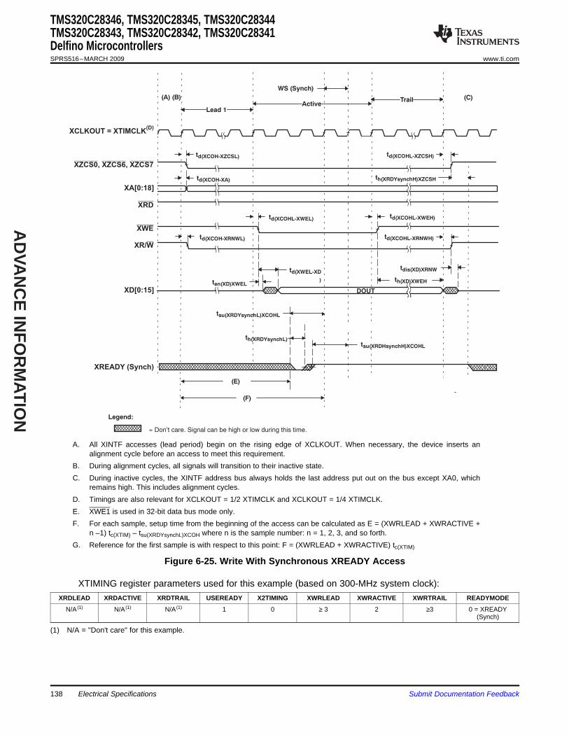
AD
VAN
CE
INF
OR
MA
TIO
N
Lead 1Active
Trail
XCLKOUT = XTIMCLK(D)
XA[0:18]
XREADY (Synch)
XD[0:15]
XR/W
XWE
XRD
XZCS0 XZCS6 XZCS7, ,
td(XCOHL-XWEL) td(XCOHL-XWEH)
td(XCOHL-XZCSH)
td(XCOH-XA)
WS (Synch)
td(XCOH-XZCSL)
td(XCOH-XRNWL) td(XCOHL-XRNWH)
ten(XD)XWELth(XD)XWEH
tsu(XRDHsynchH)XCOHL
tsu(XRDYsynchL)XCOHL
DOUT
td(XWEL-XD
)
tdis(XD)XRNW
th(XRDYsynchL)
th(XRDYsynchH)XZCSH
= Don’t care. Signal can be high or low during this time.
Legend:
(F)
(E)
(A) (B) (C)
TMS320C28346, TMS320C28345, TMS320C28344TMS320C28343, TMS320C28342, TMS320C28341Delfino MicrocontrollersSPRS516–MARCH 2009 www.ti.com
A. All XINTF accesses (lead period) begin on the rising edge of XCLKOUT. When necessary, the device inserts analignment cycle before an access to meet this requirement.
B. During alignment cycles, all signals will transition to their inactive state.C. During inactive cycles, the XINTF address bus always holds the last address put out on the bus except XA0, which
remains high. This includes alignment cycles.D. Timings are also relevant for XCLKOUT = 1/2 XTIMCLK and XCLKOUT = 1/4 XTIMCLK.E. XWE1 is used in 32-bit data bus mode only.F. For each sample, setup time from the beginning of the access can be calculated as E = (XWRLEAD + XWRACTIVE +
n –1) tc(XTIM) – tsu(XRDYsynchL)XCOH where n is the sample number: n = 1, 2, 3, and so forth.G. Reference for the first sample is with respect to this point: F = (XWRLEAD + XWRACTIVE) tc(XTIM)
Figure 6-25. Write With Synchronous XREADY Access
XTIMING register parameters used for this example (based on 300-MHz system clock):XRDLEAD XRDACTIVE XRDTRAIL USEREADY X2TIMING XWRLEAD XWRACTIVE XWRTRAIL READYMODE
N/A (1) N/A (1) N/A (1) 1 0 ≥ 3 2 ≥3 0 = XREADY(Synch)
(1) N/A = "Don't care" for this example.
Electrical Specifications138 Submit Documentation Feedback

AD
VAN
CE
INF
OR
MA
TIO
N
Lead 1
ActiveTrail
XCLKOUT = XTIMCLK(D)
XA[0:19]
td(XCOHL-XWEH)
td(XCOHL-XZCSH)
td(XCOH-XA)
WS (Async)
XZCS0 XZCS6 XZCS7, ,
XRD
XWE0, XWE1(E)
XR/W
td(XCOH-XZCSL)
td(XCOH-XRNWL) td(XCOHL-XRNWH)
ten(XD)XWELth(XD)XWEH
th(XRDYasynchL)
DOUT
tdis(XD)XRNW
th(XRDYasynchH)XZCSH
(G)
(F)
= Don’t care. Signal can be high or low during this time.
Legend:
tsu(XRDYasynchL)XCOHL
tsu(XRDYasynchH)XCOHL
td(XWEL-XD
)
td(XCOHL-XWEL)
(A) (B) (C)
XREADY(Asynch)
XD[31:0], XD[15:0]
TMS320C28346, TMS320C28345, TMS320C28344TMS320C28343, TMS320C28342, TMS320C28341
Delfino Microcontrollerswww.ti.com SPRS516–MARCH 2009
A. All XINTF accesses (lead period) begin on the rising edge of XCLKOUT. When necessary, the device inserts analignment cycle before an access to meet this requirement.
B. During alignment cycles, all signals transition to their inactive state.C. During inactive cycles, the XINTF address bus always holds the last address put out on the bus except XA0, which
remains high. This includes alignment cycles.D. Timings are also relevant for XCLKOUT = 1/2 XTIMCLK and XCLKOUT = 1/4 XTIMCLK.E. XWE1 is used in 32-bit data bus mode only.F. For each sample, set up time from the beginning of the access can be calculated as: E = (XWRLEAD + XWRACTIVE
-3 + n) tc(XTIM) – tsu(XRDYasynchL)XCOHL where n is the sample number: n = 1, 2, 3, and so forth.G. Reference for the first sample is with respect to this point: F = (XWRLEAD + XWRACTIVE – 2) tc(XTIM)
Figure 6-26. Write With Asynchronous XREADY Access
XTIMING register parameters used for this example (based on 300-MHz system clock):XRDLEAD XRDACTIVE XRDTRAIL USEREADY X2TIMING XWRLEAD XWRACTIVE XWRTRAIL READYMODE
N/A (1) N/A (1) N/A (1) 1 0 ≥ 3 4 ≥ 3 1 = XREADY(Async)
(1) N/A = “Don’t care” for this example
Submit Documentation Feedback Electrical Specifications 139

AD
VAN
CE
INF
OR
MA
TIO
N
6.15.9 XHOLD and XHOLDA Timing
TMS320C28346, TMS320C28345, TMS320C28344TMS320C28343, TMS320C28342, TMS320C28341Delfino MicrocontrollersSPRS516–MARCH 2009 www.ti.com
If the HOLD mode bit is set while XHOLD and XHOLDA are both low (external bus accesses granted), theXHOLDA signal is forced high (at the end of the current cycle) and the external interface is taken out ofhigh-impedance mode.
On a reset (XRS), the HOLD mode bit is set to 0. If the XHOLD signal is active low on a system reset, thebus and all signal strobes must be in high-impedance mode, and the XHOLDA signal is also driven activelow.
When HOLD mode is enabled and XHOLDA is active low (external bus grant active), the CPU can stillexecute code from internal memory. If an access is made to the external interface, the CPU is stalled untilthe XHOLD signal is removed.
An external DMA request, when granted, places the following signals in a high-impedance mode:
XA[19:0] XZCS0XD[31:0], XD[15:0] XZCS6XWE0, XWE1, XZCS7XRDXR/W
All other signals not listed in this group remain in their default or functional operational modes during thesesignal events.
Table 6-47. XHOLD/XHOLDA Timing Requirements (1) (2) (3)
MIN MAX UNITtd(HL-HiZ) Delay time, XHOLD low to Hi-Z on all address, data, and control 4tc(XTIM) + tc(XCO) nstd(HL-HAL) Delay time, XHOLD low to XHOLDA low 4tc(XTIM + 2tc(XCO) nstd(HH-HAH) Delay time, XHOLD high to XHOLDA high 4tc(XTIM) nstd(HH-BV) Delay time, XHOLD high to bus valid 6tc(XTIM) ns
(1) When a low signal is detected on XHOLD, all pending XINTF accesses will be completed before the bus is placed in a high-impedancestate.
(2) The state of XHOLD is latched on the rising edge of XTIMCLK.(3) After the XHOLD is detected low or high, all bus transitions and XHOLDA transitions occur with respect to the rising edge of XCLKOUT.
Thus, for this mode where XCLKOUT = 1/2 XTIMCLK, the transitions can occur up to 1 XTIMCLK cycle earlier than the maximum valuespecified.
Electrical Specifications140 Submit Documentation Feedback

AD
VAN
CE
INF
OR
MA
TIO
N
XCLKOUT
XHOLD
XZCS0 XZCS6 XZCS7, ,
XD[31:0], XD[15:0] Valid
XHOLDA
td(HL-Hiz)
td(HH-HAH)
High-Impedance
XA[19:0] Valid ValidHigh-Impedance
td(HH-BV)td(HL-HAL)
(A)(B)
XR/W
TMS320C28346, TMS320C28345, TMS320C28344TMS320C28343, TMS320C28342, TMS320C28341
Delfino Microcontrollerswww.ti.com SPRS516–MARCH 2009
A. All pending XINTF accesses are completed.B. Normal XINTF operation resumes.
Figure 6-27. External Interface Hold Waveform
Submit Documentation Feedback Electrical Specifications 141

(2) 2P = 1/CLKG in ns. CLKG is the output of sample rate generator mux. CLKG =CLKSRG
(1 CLKGDV) CLKSRG can be LSPCLK, CLKX, CLKR
AD
VAN
CE
INF
OR
MA
TIO
N
6.16 Multichannel Buffered Serial Port (McBSP) Timing
6.16.1 McBSP Transmit and Receive Timing
TMS320C28346, TMS320C28345, TMS320C28344TMS320C28343, TMS320C28342, TMS320C28341Delfino MicrocontrollersSPRS516–MARCH 2009 www.ti.com
Table 6-48. McBSP Timing Requirements (1) (2)
NO. MIN MAX UNITMcBSP module clock (CLKG, CLKX, CLKR) range 1 kHz
40 (3) MHzMcBSP module cycle time (CLKG, CLKX, CLKR) range 25 ns
1 msM11 tc(CKRX) Cycle time, CLKR/X CLKR/X ext 2P nsM12 tw(CKRX) Pulse duration, CLKR/X high or CLKR/X low CLKR/X ext P – 4 nsM13 tr(CKRX) Rise time, CLKR/X CLKR/X ext 4 nsM14 tf(CKRX) Fall time, CLKR/X CLKR/X ext 4 nsM15 tsu(FRH-CKRL) Setup time, external FSR high before CLKR low CLKR int 20 ns
CLKR ext 2M16 th(CKRL-FRH) Hold time, external FSR high after CLKR low CLKR int 0 ns
CLKR ext 6M17 tsu(DRV-CKRL) Setup time, DR valid before CLKR low CLKR int 20 ns
CLKR ext 2M18 th(CKRL-DRV) Hold time, DR valid after CLKR low CLKR int 0 ns
CLKR ext 6M19 tsu(FXH-CKXL) Setup time, external FSX high before CLKX low CLKX int 20 ns
CLKX ext 2M20 th(CKXL-FXH) Hold time, external FSX high after CLKX low CLKX int 0 ns
CLKX ext 6
(1) Polarity bits CLKRP = CLKXP = FSRP = FSXP = 0. If the polarity of any of the signals is inverted, then the timing references of thatsignal are also inverted.
as source. CLKSRG ≤ (SYSCLKOUT/2). McBSP performance is limited by I/O buffer switching speed.(3) Internal clock prescalers must be adjusted such that the McBSP clock (CLKG, CLKX, CLKR) speeds are not greater than the I/O buffer
speed limit (40 MHz).
142 Electrical Specifications Submit Documentation Feedback

AD
VAN
CE
INF
OR
MA
TIO
N
TMS320C28346, TMS320C28345, TMS320C28344TMS320C28343, TMS320C28342, TMS320C28341
Delfino Microcontrollerswww.ti.com SPRS516–MARCH 2009
Table 6-49. McBSP Switching Characteristics (1) (2)
NO. PARAMETER MIN MAX UNITM1 tc(CKRX) Cycle time, CLKR/X CLKR/X int 2P nsM2 tw(CKRXH) Pulse duration, CLKR/X high CLKR/X int D – 2 (3) D + 2 (3) nsM3 tw(CKRXL) Pulse duration, CLKR/X low CLKR/X int C – 2 (3) C + 2 (3) nsM4 td(CKRH-FRV) Delay time, CLKR high to internal FSR valid CLKR int 0 4 ns
CLKR ext 3 20M5 td(CKXH-FXV) Delay time, CLKX high to internal FSX valid CLKX int 0 4 ns
CLKX ext 3 20M6 tdis(CKXH-DXHZ) Disable time, CLKX high to DX high impedance CLKX int 8 ns
following last data bit CLKX ext 14M7 td(CKXH-DXV) Delay time, CLKX high to DX valid. CLKX int 4 ns
This applies to all bits except the first bit transmitted. CLKX ext 20Delay time, CLKX high to DX valid DXENA = 0 CLKX int 4
CLKX ext 20Only applies to first bit transmitted when DXENA = 1 CLKX int P + 4in Data Delay 1 or 2 (XDATDLY=01b or CLKX ext P + 2010b) modes
M8 ten(CKXH-DX) Enable time, CLKX high to DX driven DXENA = 0 CLKX int 0 nsCLKX ext 10
Only applies to first bit transmitted when DXENA = 1 CLKX int Pin Data Delay 1 or 2 (XDATDLY=01b or CLKX ext P + 1010b) modes
M9 td(FXH-DXV) Delay time, FSX high to DX valid DXENA = 0 FSX int 4 nsFSX ext 16
Only applies to first bit transmitted when DXENA = 1 FSX int P + 4in Data Delay 0 (XDATDLY=00b) mode. FSX ext P + 16
M10 ten(FXH-DX) Enable time, FSX high to DX driven DXENA = 0 FSX int 0 nsFSX ext 6
Only applies to first bit transmitted when DXENA = 1 FSX int Pin Data Delay 0 (XDATDLY=00b) mode FSX ext P + 6
(1) Polarity bits CLKRP = CLKXP = FSRP = FSXP = 0. If the polarity of any of the signals is inverted, then the timing references of thatsignal are also inverted.
(2) 2P = 1/CLKG in ns.(3) C=CLKRX low pulse width = P
D=CLKRX high pulse width = P
Submit Documentation Feedback Electrical Specifications 143

AD
VAN
CE
INF
OR
MA
TIO
N
(n−2)Bit (n−1)
(n−3)(n−2)Bit (n−1)
(n−4)(n−3)(n−2)Bit (n−1)
M18M17
M18M17
M17M18
M16M15
M4M4M14
M13M3, M12
M1, M11
M2, M12
(RDATDLY=10b)DR
(RDATDLY=01b)DR
(RDATDLY=00b)DR
FSR (ext)
FSR (int)
CLKR
M8
M7
M7M8
M6
M7M9
M10
(XDATDLY=10b)DX
(XDATDLY=01b)DX
(XDATDLY=00b)DX
Bit (n−1)Bit 0
Bit (n−1) (n−3)(n−2)Bit 0
(n−2)Bit (n−1)Bit 0
M20
M13M3, M12
M1, M11M2, M12
FSX (ext)
FSX (int)
CLKX
M5M5
M19
TMS320C28346, TMS320C28345, TMS320C28344TMS320C28343, TMS320C28342, TMS320C28341Delfino MicrocontrollersSPRS516–MARCH 2009 www.ti.com
Figure 6-28. McBSP Receive Timing
Figure 6-29. McBSP Transmit Timing
144 Electrical Specifications Submit Documentation Feedback

AD
VAN
CE
INF
OR
MA
TIO
N
6.16.2 McBSP as SPI Master or Slave Timing
Bit 0 Bit(n-1) (n-2) (n-3) (n-4)
Bit 0 Bit(n-1) (n-2) (n-3) (n-4)
CLKX
FSX
DX
M30M31
DR
M28
M24
M29
M25
LSB MSBM32 M33
TMS320C28346, TMS320C28345, TMS320C28344TMS320C28343, TMS320C28342, TMS320C28341
Delfino Microcontrollerswww.ti.com SPRS516–MARCH 2009
Table 6-50. McBSP as SPI Master or Slave Timing Requirements (CLKSTP = 10b, CLKXP = 0)MASTER SLAVE
NO. UNITMIN MAX MIN MAX
M30 tsu(DRV-CKXL) Setup time, DR valid before CLKX low 30 8P – 10 nsM31 th(CKXL-DRV) Hold time, DR valid after CLKX low 1 8P –10 nsM32 tsu(BFXL-CKXH) Setup time, FSX low before CLKX high 8P + 10 nsM33 tc(CKX) Cycle time, CLKX 2P (1) 16P ns
(1) 2P = 1/CLKG
Table 6-51. McBSP as SPI Master or Slave Switching Characteristics (CLKSTP = 10b, CLKXP = 0)MASTER SLAVE
NO. PARAMETER UNITMIN MAX MIN MAX
M24 th(CKXL-FXL) Hold time, FSX low after CLKX low 2P (1) nsM25 td(FXL-CKXH) Delay time, FSX low to CLKX high P nsM28 tdis(FXH-DXHZ) Disable time, DX high impedance following last data bit from 6 6P + 6 ns
FSX highM29 td(FXL-DXV) Delay time, FSX low to DX valid 6 4P + 6 ns
(1) 2P = 1/CLKG
For all SPI slave modes, CLKX has to be minimum 8 CLKG cycles. Also CLKG should be LSPCLK/2 bysetting CLKSM = CLKGDV = 1. With maximum LSPCLK speed of 150 MHz, CLKX maximum frequencywill be LSPCLK/16 , that is 9.375 MHz and P = 6.67 ns.
Figure 6-30. McBSP Timing as SPI Master or Slave: CLKSTP = 10b, CLKXP = 0
Submit Documentation Feedback Electrical Specifications 145

AD
VAN
CE
INF
OR
MA
TIO
N Bit 0 Bit(n-1) (n-2) (n-3) (n-4)
Bit 0 Bit(n-1) (n-2) (n-3) (n-4)
CLKX
FSX
DX
DR
M35
M37
M40M39
M38
M34
LSB MSBM41 M42
TMS320C28346, TMS320C28345, TMS320C28344TMS320C28343, TMS320C28342, TMS320C28341Delfino MicrocontrollersSPRS516–MARCH 2009 www.ti.com
Table 6-52. McBSP as SPI Master or Slave Timing Requirements (CLKSTP = 11b, CLKXP = 0)MASTER SLAVE
NO. UNITMIN MAX MIN MAX
M39 tsu(DRV-CKXH) Setup time, DR valid before CLKX high 30 8P – 10 nsM40 th(CKXH-DRV) Hold time, DR valid after CLKX high 1 8P – 10 nsM41 tsu(FXL-CKXH) Setup time, FSX low before CLKX high 16P + 10 nsM42 tc(CKX) Cycle time, CLKX 2P (1) 16P ns
(1) 2P = 1/CLKG
Table 6-53. McBSP as SPI Master or Slave Switching Characteristics (CLKSTP = 11b, CLKXP = 0)MASTER SLAVE
NO. PARAMETER UNITMIN MAX MIN MAX
M34 th(CKXL-FXL) Hold time, FSX low after CLKX low P nsM35 td(FXL-CKXH) Delay time, FSX low to CLKX high 2P (1) nsM37 tdis(CKXL-DXHZ) Disable time, DX high impedance following last data bit P + 6 7P + 6 ns
from CLKX lowM38 td(FXL-DXV) Delay time, FSX low to DX valid 6 4P + 6 ns
(1) 2P = 1/CLKG
For all SPI slave modes, CLKX must be a minimum of 8 CLKG cycles. Also, CLKG should be LSPCLK/2by setting CLKSM = CLKGDV = 1. With a maximum LSPCLK speed of 150 MHz, CLKX maximumfrequency is LSPCLK/16; that is, 9.375 MHz and P =6.67 ns.
Figure 6-31. McBSP Timing as SPI Master or Slave: CLKSTP = 11b, CLKXP = 0
Electrical Specifications146 Submit Documentation Feedback

AD
VAN
CE
INF
OR
MA
TIO
N
M51
M50
M47
Bit 0 Bit(n-1) (n-2) (n-3) (n-4)
Bit 0 Bit(n-1) (n-2) (n-3) (n-4)
CLKX
FSX
DX
DR
M44
M48
M49
M43
LSB MSB M52
TMS320C28346, TMS320C28345, TMS320C28344TMS320C28343, TMS320C28342, TMS320C28341
Delfino Microcontrollerswww.ti.com SPRS516–MARCH 2009
Table 6-54. McBSP as SPI Master or Slave Timing Requirements (CLKSTP = 10b, CLKXP = 1)MASTER SLAVE
NO. UNITMIN MAX MIN MAX
M49 tsu(DRV-CKXH) Setup time, DR valid before CLKX high 30 8P –10 nsM50 th(CKXH-DRV) Hold time, DR valid after CLKX high 1 8P –10 nsM51 tsu(FXL-CKXL) Setup time, FSX low before CLKX low 8P + 10 nsM52 tc(CKX) Cycle time, CLKX 2P (1) 16P ns
(1) 2P = 1/CLKG
Table 6-55. McBSP as SPI Master or Slave Switching Characteristics (CLKSTP = 10b, CLKXP = 1)MASTER SLAVE
NO. PARAMETER UNITMIN MAX MIN MAX
M43 th(CKXH-FXL) Hold time, FSX low after CLKX high 2P (1) nsM44 td(FXL-CKXL) Delay time, FSX low to CLKX low P nsM47 tdis(FXH-DXHZ) Disable time, DX high impedance following last data bit from 6 6P + 6 ns
FSX highM48 td(FXL-DXV) Delay time, FSX low to DX valid 6 4P + 6 ns
(1) 2P = 1/CLKG
For all SPI slave modes, CLKX must be a minimum of 8 CLKG cycles. Also, CLKG should be LSPCLK/2by setting CLKSM = CLKGDV = 1. With maximum LSPCLK speed of 150 MHz, CLKX maximumfrequency will be LSPCLK/16; that is, 9.375 MHz and P = 6.67 ns.
Figure 6-32. McBSP Timing as SPI Master or Slave: CLKSTP = 10b, CLKXP = 1
Submit Documentation Feedback Electrical Specifications 147

AD
VAN
CE
INF
OR
MA
TIO
N
Bit 0 Bit(n-1) (n-2) (n-3) (n-4)
Bit 0 Bit(n-1) (n-2) (n-3) (n-4)
CLKX
FSX
DX
DR
M54
M58
M56
M53
M55
M59
M57
LSB MSBM60 M61
TMS320C28346, TMS320C28345, TMS320C28344TMS320C28343, TMS320C28342, TMS320C28341Delfino MicrocontrollersSPRS516–MARCH 2009 www.ti.com
Table 6-56. McBSP as SPI Master or Slave Timing Requirements (CLKSTP = 11b, CLKXP = 1)MASTER SLAVE
NO. UNITMIN MAX MIN MAX
M58 tsu(DRV-CKXL) Setup time, DR valid before CLKX low 30 8P – 10 nsM59 th(CKXL-DRV) Hold time, DR valid after CLKX low 1 8P – 10 nsM60 tsu(FXL-CKXL) Setup time, FSX low before CLKX low 16P + 10 nsM61 tc(CKX) Cycle time, CLKX 2P (1) 16P ns
(1) 2P = 1/CLKG
For all SPI slave modes, CLKX must be a minimum of 8 CLKG cycles. Also CLKG should be LSPCLK/2by setting CLKSM = CLKGDV = 1. With maximum LSPCLK speed of 150 MHz, CLKX maximumfrequency is LSPCLK/16 , that is 9.375 MHz and P = 6.67 ns.
Table 6-57. McBSP as SPI Master or Slave Switching Characteristics (CLKSTP = 11b, CLKXP = 1) (1)
MASTER (2) SLAVENO. PARAMETER UNIT
MIN MAX MIN MAXM53 th(CKXH-FXL) Hold time, FSX low after CLKX high P nsM54 td(FXL-CKXL) Delay time, FSX low to CLKX low 2P (1) nsM56 tdis(CKXH-DXHZ) Disable time, DX high impedance following last data bit from P + 6 7P + 6 ns
CLKX highM57 td(FXL-DXV) Delay time, FSX low to DX valid 6 4P + 6 ns
(1) 2P = 1/CLKG(2) C = CLKX low pulse width = P
D = CLKX high pulse width = P
Figure 6-33. McBSP Timing as SPI Master or Slave: CLKSTP = 11b, CLKXP = 1
Electrical Specifications148 Submit Documentation Feedback

AD
VAN
CE
INF
OR
MA
TIO
N
7 Thermal/Mechanical Data
TMS320C28346, TMS320C28345, TMS320C28344TMS320C28343, TMS320C28342, TMS320C28341
Delfino Microcontrollerswww.ti.com SPRS516–MARCH 2009
Table 7-1 and Table 7-2 show the thermal data.
The mechanical package diagram(s) that follow the tables reflect the most current released mechanicaldata available for the designated device(s).
Table 7-1. Thermal Model 179-Ball ZHH ResultsAIR FLOW
PARAMETER 0 lfm 150 lfm 250 lfm 500 lfmθJA[°C/W] High k PCB 40.8 32.4 31.0 29.1
ΨJT[°C/W] 0.4 0.5 0.6 0.8ΨJB 21.0 20.4 20.2 19.9θJC 10.3θJB 21.2
Table 7-2. Thermal Model 256-Ball ZFE ResultsAIR FLOW
PARAMETER 0 lfm 150 lfm 250 lfm 500 lfmθJA[°C/W] High k PCB 30 21.8 20.6 19.1
ΨJT[°C/W] 1.24 2.63 3.15 4.05ΨJB 14 13.6 13.5 13.4θJC 14θJB 13.9
Submit Documentation Feedback Thermal/Mechanical Data 149

PACKAGING INFORMATION
Orderable Device Status (1) PackageType
PackageDrawing
Pins PackageQty
Eco Plan (2) Lead/Ball Finish MSL Peak Temp (3)
TMX320C28343ZHH ACTIVE BGA MI CROSTA
R
ZHH 179 1 TBD Call TI Call TI
TMX320C28346ZEP ACTIVE BGA ZEP 256 1 TBD Call TI Call TI
(1) The marketing status values are defined as follows:ACTIVE: Product device recommended for new designs.LIFEBUY: TI has announced that the device will be discontinued, and a lifetime-buy period is in effect.NRND: Not recommended for new designs. Device is in production to support existing customers, but TI does not recommend using this part ina new design.PREVIEW: Device has been announced but is not in production. Samples may or may not be available.OBSOLETE: TI has discontinued the production of the device.
(2) Eco Plan - The planned eco-friendly classification: Pb-Free (RoHS), Pb-Free (RoHS Exempt), or Green (RoHS & no Sb/Br) - please checkhttp://www.ti.com/productcontent for the latest availability information and additional product content details.TBD: The Pb-Free/Green conversion plan has not been defined.Pb-Free (RoHS): TI's terms "Lead-Free" or "Pb-Free" mean semiconductor products that are compatible with the current RoHS requirementsfor all 6 substances, including the requirement that lead not exceed 0.1% by weight in homogeneous materials. Where designed to be solderedat high temperatures, TI Pb-Free products are suitable for use in specified lead-free processes.Pb-Free (RoHS Exempt): This component has a RoHS exemption for either 1) lead-based flip-chip solder bumps used between the die andpackage, or 2) lead-based die adhesive used between the die and leadframe. The component is otherwise considered Pb-Free (RoHScompatible) as defined above.Green (RoHS & no Sb/Br): TI defines "Green" to mean Pb-Free (RoHS compatible), and free of Bromine (Br) and Antimony (Sb) based flameretardants (Br or Sb do not exceed 0.1% by weight in homogeneous material)
(3) MSL, Peak Temp. -- The Moisture Sensitivity Level rating according to the JEDEC industry standard classifications, and peak soldertemperature.
Important Information and Disclaimer:The information provided on this page represents TI's knowledge and belief as of the date that it isprovided. TI bases its knowledge and belief on information provided by third parties, and makes no representation or warranty as to theaccuracy of such information. Efforts are underway to better integrate information from third parties. TI has taken and continues to takereasonable steps to provide representative and accurate information but may not have conducted destructive testing or chemical analysis onincoming materials and chemicals. TI and TI suppliers consider certain information to be proprietary, and thus CAS numbers and other limitedinformation may not be available for release.
In no event shall TI's liability arising out of such information exceed the total purchase price of the TI part(s) at issue in this document sold by TIto Customer on an annual basis.
PACKAGE OPTION ADDENDUM
www.ti.com 3-Mar-2009
Addendum-Page 1


IMPORTANT NOTICETexas Instruments Incorporated and its subsidiaries (TI) reserve the right to make corrections, modifications, enhancements, improvements,and other changes to its products and services at any time and to discontinue any product or service without notice. Customers shouldobtain the latest relevant information before placing orders and should verify that such information is current and complete. All products aresold subject to TI’s terms and conditions of sale supplied at the time of order acknowledgment.TI warrants performance of its hardware products to the specifications applicable at the time of sale in accordance with TI’s standardwarranty. Testing and other quality control techniques are used to the extent TI deems necessary to support this warranty. Except wheremandated by government requirements, testing of all parameters of each product is not necessarily performed.TI assumes no liability for applications assistance or customer product design. Customers are responsible for their products andapplications using TI components. To minimize the risks associated with customer products and applications, customers should provideadequate design and operating safeguards.TI does not warrant or represent that any license, either express or implied, is granted under any TI patent right, copyright, mask work right,or other TI intellectual property right relating to any combination, machine, or process in which TI products or services are used. Informationpublished by TI regarding third-party products or services does not constitute a license from TI to use such products or services or awarranty or endorsement thereof. Use of such information may require a license from a third party under the patents or other intellectualproperty of the third party, or a license from TI under the patents or other intellectual property of TI.Reproduction of TI information in TI data books or data sheets is permissible only if reproduction is without alteration and is accompaniedby all associated warranties, conditions, limitations, and notices. Reproduction of this information with alteration is an unfair and deceptivebusiness practice. TI is not responsible or liable for such altered documentation. Information of third parties may be subject to additionalrestrictions.Resale of TI products or services with statements different from or beyond the parameters stated by TI for that product or service voids allexpress and any implied warranties for the associated TI product or service and is an unfair and deceptive business practice. TI is notresponsible or liable for any such statements.TI products are not authorized for use in safety-critical applications (such as life support) where a failure of the TI product would reasonablybe expected to cause severe personal injury or death, unless officers of the parties have executed an agreement specifically governingsuch use. Buyers represent that they have all necessary expertise in the safety and regulatory ramifications of their applications, andacknowledge and agree that they are solely responsible for all legal, regulatory and safety-related requirements concerning their productsand any use of TI products in such safety-critical applications, notwithstanding any applications-related information or support that may beprovided by TI. Further, Buyers must fully indemnify TI and its representatives against any damages arising out of the use of TI products insuch safety-critical applications.TI products are neither designed nor intended for use in military/aerospace applications or environments unless the TI products arespecifically designated by TI as military-grade or "enhanced plastic." Only products designated by TI as military-grade meet militaryspecifications. Buyers acknowledge and agree that any such use of TI products which TI has not designated as military-grade is solely atthe Buyer's risk, and that they are solely responsible for compliance with all legal and regulatory requirements in connection with such use.TI products are neither designed nor intended for use in automotive applications or environments unless the specific TI products aredesignated by TI as compliant with ISO/TS 16949 requirements. Buyers acknowledge and agree that, if they use any non-designatedproducts in automotive applications, TI will not be responsible for any failure to meet such requirements.Following are URLs where you can obtain information on other Texas Instruments products and application solutions:Products ApplicationsAmplifiers amplifier.ti.com Audio www.ti.com/audioData Converters dataconverter.ti.com Automotive www.ti.com/automotiveDLP® Products www.dlp.com Broadband www.ti.com/broadbandDSP dsp.ti.com Digital Control www.ti.com/digitalcontrolClocks and Timers www.ti.com/clocks Medical www.ti.com/medicalInterface interface.ti.com Military www.ti.com/militaryLogic logic.ti.com Optical Networking www.ti.com/opticalnetworkPower Mgmt power.ti.com Security www.ti.com/securityMicrocontrollers microcontroller.ti.com Telephony www.ti.com/telephonyRFID www.ti-rfid.com Video & Imaging www.ti.com/videoRF/IF and ZigBee® Solutions www.ti.com/lprf Wireless www.ti.com/wireless
Mailing Address: Texas Instruments, Post Office Box 655303, Dallas, Texas 75265Copyright © 2009, Texas Instruments Incorporated