tms320c54xx evaluation module technical referenceread.pudn.com/downloads74/doc/269753/evm...
TRANSCRIPT

TMS320C54XXEvaluation Module
2001 DSP Development Systems
ReferenceTechnical

TMS320C54XX Evaluation Module
Technical Reference
503482-0001 Rev. I March 2001
SPECTRUM DIGITAL, INC.12502 Exchange Drive, Suite 440 Stafford, TX. 77477
Tel: 281.494.4505 Fax: [email protected] www.spectrumdigital.com

IMPORTANT NOTICE
Spectrum Digital, Inc. reserves the right to make changes to its products or to discontinue anyproduct or service without notice. Customers are advised to obtain the latest version of relevantinformation to verifythat the data being relied on is current before placing orders.
Spectrum Digital, Inc. warrants performance of its products and related software to currentspecifications in accordance with Spectrum Digital’s standard warranty. Testing and other qualitycontrol techniques are utilized to the extent deemed necessary to support this warranty.
Please be aware that the products described herein are not intended for use in life-support appliances, devices, or systems. Spectrum Digital does not warrant nor is Spectrum Digital liable for the product described herein to be used in other than a development environment.
Spectrum Digital, Inc. assumes no liability for applications assistance, customer product design, software performance, or infringement of patents or services described herein. Nor does SpectrumDigital warrant or represent any license, either express or implied, is granted under any patent right,copyright, or other intellectual property right of Spectrum Digital, Inc. covering or relating to anycombination, machine, or process in which such Digital Signal Processing development products orservices might be or are used.
WARNING
This equipment is intended for use in a laboratory test environment only. It generates, uses, and canradiate radio frequency energy and has not been tested for compliance with the limits of computingdevices pursuant to subpart J of part 15 of FCC rules, which are designed to provide reasonableprotection against radio frequency interference. Operation of this equipment in other environmentsmay cause interference with radio communications, in which case the user at his own expense will berequired to take whatever measures necessary to correct this interference.
TRADEMARKSMS-DOS, MS-Windows, Windows 95, Windows 98, and Windows NT are registered trademarks of Microsoft Corp.
Copyright © 2000, 2001 Spectrum Digital, Inc.
Contents
1 Introduction to the TMS320C54XX Evaluation Module . . . . . . . . . . . . . . . . . . . . . . . . . . . 1-1 Provides you with a description of the TMS320C54XX Evaluation Module, key features, and board outline. 1.0 Overview of the TMS320C54XX EVM . . . . . . . . . . . . . . . . . . . . . . . . . . . . . . . . . . . . . . . 1-2 1.1 Key Features of the TMS320C54XX EVM . . . . . . . . . . . . . . . . . . . . . . . . . . . . . . . . . . . 1-2 1.2 Functional Overview of the TMS320C54XX EVM . . . . . . . . . . . . . . . . . . . . . . . . . . . . . . 1-32 TMS320C54XX EVM Operation . . . . . . . . . . . . . . . . . . . . . . . . . . . . . . . . . . . . . . . . . . . . . . . 2-1 Describes the operation of the EVM320C54XX. Information is provided on the EVM’s various interfaces. 2.0 The TMS320C54XX EVM Operation . . . . . . . . . . . . . . . . . . . . . . . . . . . . . . . . . . . . . . . . 2-3 2.1 The TMS320C54XX EVM Board . . . . . . . . . . . . . . . . . . . . . . . . . . . . . . . . . . . . . . . . . . 2-3 2.1.1 Power Connector . . . . . . . . . . . . . . . . . . . . . . . . . . . . . . . . . . . . . . . . . . . . . . . . . . . . . 2-4 2.2 TMS320C54XX Memory Interface . . . . . . . . . . . . . . . . . . . . . . . . . . . . . . . . . . . . . . . . . . 2-4 2.2.1 Program Memory . . . . . . . . . . . . . . . . . . . . . . . . . . . . . . . . . . . . . . . . . . . . . . . . . . . . . . 2-6 2.2.2 Data Memory . . . . . . . . . . . . . . . . . . . . . . . . . . . . . . . . . . . . . . . . . . . . . . . . . . . . . . . . . 2-10 2.2.3 I/O Space . . . . . . . . . . . . . . . . . . . . . . . . . . . . . . . . . . . . . . . . . . . . . . . . . . . . . . . . . . . . 2-12 2.3 Onboard UART . . . . . . . . . . . . . . . . . . . . . . . . . . . . . . . . . . . . . . . . . . . . . . . . . . . . . . . . . 2-12 2.4 Oscillator Selection . . . . . . . . . . . . . . . . . . . . . . . . . . . . . . . . . . . . . . . . . . . . . . . . . . . . 2-12 2.5 Analog Interface . . . . . . . . . . . . . . . . . . . . . . . . . . . . . . . . . . . . . . . . . . . . . . . . . . . . . . . 2-13 2.5.1 J2, Analog Input . . . . . . . . . . . . . . . . . . . . . . . . . . . . . . . . . . . . . . . . . . . . . . . . . . . . . 2-13 2.5.2 J3, Analog Output . . . . . . . . . . . . . . . . . . . . . . . . . . . . . . . . . . . . . . . . . . . . . . . . . . . . 2-13 2.6 Expansion Bus . . . . . . . . . . . . . . . . . . . . . . . . . . . . . . . . . . . . . . . . . . . . . . . . . . . . . . . . 2-14 2.6.1 P1, I/O Expansion Connector . . . . . . . . . . . . . . . . . . . . . . . . . . . . . . . . . . . . . . . . . . . . 2-15 2.6.1.1 P1, I/O Expansion Connector for LC548, LC549, VC549 . . . . . . . . . . . . . . . . . . . . . 2-15 2.6.1.2 P1, I/O Expansion Connector for VC5402 . . . . . . . . . . . . . . . . . . . . . . . . . . . . . . . . 2-16 2.6.1.3 P1, I/O Expansion Connector for VC5410 . . . . . . . . . . . . . . . . . . . . . . . . . . . . . . . . 2-17 2.6.2 P2, Analog Expansion Connector . . . . . . . . . . . . . . . . . . . . . . . . . . . . . . . . . . . . . . . . . 2-18 2.6.3 P3, Address/Data Expansion Connector . . . . . . . . . . . . . . . . . . . . . . . . . . . . . . . . . . . 2-19 2.6.4 P4, Control Expansion Connector . . . . . . . . . . . . . . . . . . . . . . . . . . . . . . . . . . . . . . . . . 2-20 2.6.4.1 P4, Control Expansion Connector for LC548, LC549, VC549, VC5410 . . . . . . . . 2-20 2.6.4.2 P4, Control Expansion Connector for VC5402 . . . . . . . . . . . . . . . . . . . . . . . . . . . . . 2-21 2.6.5 P6, Host Port Interface Expansion Connector . . . . . . . . . . . . . . . . . . . . . . . . . . . . . . . 2-22 2.7 P7, JTAG Interface . . . . . . . . . . . . . . . . . . . . . . . . . . . . . . . . . . . . . . . . . . . . . . . . . . . . . 2-23 2.8 Onboard Serial Interface . . . . . . . . . . . . . . . . . . . . . . . . . . . . . . . . . . . . . . . . . . . . . . . . 2-24 2.9 Boot Loading . . . . . . . . . . . . . . . . . . . . . . . . . . . . . . . . . . . . . . . . . . . . . . . . . . . . . . . . . . 2-25 2.10 EVM320C54X EVM Jumpers . . . . . . . . . . . . . . . . . . . . . . . . . . . . . . . . . . . . . . . . . . . . 2-27 2.10.1 Jumper Positions . . . . . . . . . . . . . . . . . . . . . . . . . . . . . . . . . . . . . . . . . . . . . . . . . . . . . 2-28 2.10.2 JP1, UART Reset . . . . . . . . . . . . . . . . . . . . . . . . . . . . . . . . . . . . . . . . . . . . . . . . . . . . 2-28 2.10.3 JP2, Onboard UART CTS Routing . . . . . . . . . . . . . . . . . . . . . . . . . . . . . . . . . . . . . 2-28 2.10.4 JP3, A15/A17 Select . . . . . . . . . . . . . . . . . . . . . . . . . . . . . . . . . . . . . . . . . . . . . . . . . 2-28
2.10.5 JP4, AD50 AC/DC Coupling . . . . . . . . . . . . . . . . . . . . . . . . . . . . . . . . . . . . . . . . . . . . . . . . . . 2-29 2.10.6 JP5, Synchronous Port Routing . . . . . . . . . . . . . . . . . . . . . . . . . . . . . . . . . . . . . . . . . . . . . . . 2-29 2.10.7 JP6, AD50 Reset . . . . . . . . . . . . . . . . . . . . . . . . . . . . . . . . . . . . . . . . . . . . . . . . . . . . . . . . . . . 2-29 2.10.8 JP7, SYSCLK Select . . . . . . . . . . . . . . . . . . . . . . . . . . . . . . . . . . . . . . . . . . . . . . . . . . . . . . . 2-30 2.10.9 JP8, AD50 Voltage Reference . . . . . . . . . . . . . . . . . . . . . . . . . . . . . . . . . . . . . . . . . . . . . . . 2-30 2.10.10 JP9, DSP Core Voltage Select . . . . . . . . . . . . . . . . . . . . . . . . . . . . . . . . . . . . . . . . . . . . . . . 2-31 2.10.11 JP10, Ready Routing . . . . . . . . . . . . . . . . . . . . . . . . . . . . . . . . . . . . . . . . . . . . . . . . . . . . . . . 2-31 2.10.12 JP11, Onboard UART Interrupt Select . . . . . . . . . . . . . . . . . . . . . . . . . . . . . . . . . . . . . . . . . 2-32 2.10.13 JP12, Voltage Select . . . . . . . . . . . . . . . . . . . . . . . . . . . . . . . . . . . . . . . . . . . . . . . . . . . . . . . 2-32 2.10.14 JP13, Bootloader Enable/Disable . . . . . . . . . . . . . . . . . . . . . . . . . . . . . . . . . . . . . . . . . . . 2-32 2.10.15 JP14, JP15, JP16, Oscillator Selection . . . . . . . . . . . . . . . . . . . . . . . . . . . . . . . . . . . . . . . 2-33 2.11 LEDS . . . . . . . . . . . . . . . . . . . . . . . . . . . . . . . . . . . . . . . . . . . . . . . . . . . . . . . . . . . . . . . . . . . . . . 2-34 2.12 Resets . . . . . . . . . . . . . . . . . . . . . . . . . . . . . . . . . . . . . . . . . . . . . . . . . . . . . . . . . . . . . . . . . . . . 2-34A TMS320C54XX EVM GAL Equations . . . . . . . . . . . . . . . . . . . . . . . . . . . . . . . . . . . . . . . . . . . . . . . . . A-1 Lists the GAL equations that are used on the TMS320C54XX EVM A.1.1 Memory Decode GAL Equations for VC5402 . . . . . . . . . . . . . . . . . . . . . . . . . . . . . . . . . . . . . . A-2 A.1.2 Memory Decode GAL Equations for LC548, LC549, VC549, VC5410 . . . . . . . . . . . . . . . . . A-4 A.1.3 Memory Decode GAL Equations for VC5416 . . . . . . . . . . . . . . . . . . . . . . . . . . . . . . . . . . . . . . A-6 A.2 I/O Control GAL Equations . . . . . . . . . . . . . . . . . . . . . . . . . . . . . . . . . . . . . . . . . . . . . . . . . . . . . . . A-8B TMS320C54XX Schematics . . . . . . . . . . . . . . . . . . . . . . . . . . . . . . . . . . . . . . . . . . . . . . . . . . . . . . . . . . B-1 Contains the schematics for the TMS320C54XX EVMC TL16C550 Data Sheet . . . . . . . . . . . . . . . . . . . . . . . . . . . . . . . . . . . . . . . . . . . . . . . . . . . . . . . . . . . . . C-1 Contains the technical information for the TL16C550D TLC320AD50 Data Sheet . . . . . . . . . . . . . . . . . . . . . . . . . . . . . . . . . . . . . . . . . . . . . . . . . . . . . . . . . . D-1 Contains the technical information for the TLC320AD50E EVM320 Mechanical Information . . . . . . . . . . . . . . . . . . . . . . . . . . . . . . . . . . . . . . . . . . . . . . . . . . . E-1 Contains the mechanical information about the TMS320C54XX EVM

About This Manual
This document describes the board level operations of the TMS320C54XX evaluationmodule (EVM). The EVM is based on the Texas Instruments TMS320C54XX DigitalSignal Processor.
The TMS320C54XX EVM is a table top card to allow engineers and softwaredevelopers to evaluate certain characteristics of the TMS320C54XX DSP to determineif the processor meets the designers application requirements. Evaluators can createsoftware to execute onboard or expand the system in a variety of ways.
Notational Conventions
This document uses the following conventions.
The TMS320C54XX will sometimes be referred to as the C54XX.
Program listings, program examples, and interactive displays are shown is a specialitalic typeface. Here is a sample program listing.
equations!rd = !strobe&rw;
Information About Cautions
This book may contain cautions.This is an example of a caution statement.A caution statement describes a situation that could potentially damage your software,or hardware, or other equipment. The information in a caution is provided for yourprotection. Please read each caution carefully.
Related Documents
Texas Instruments TMS320C54X Users GuideTexas Instruments TMS320C54X Fixed Point Assembly Language Users GuideTexas Instruments TMS320C54X Fixed Point C Language Users GuideTexas Instruments TMS320C54X Fixed Point C Source Debugger Users Guide
1-1
Chapter 1
Introduction to the TMS320C54XX Evaluation Module
Chapter One provides a description of the TMS32C54XX EvaluationModule along with the key features and a block diagram of the circuitboard.
Topic Page
1.0 Overview of the TMS320C54XX EVM 1-21.1 Key Features of the TMS320C54XX EVM 1-21.2 Functional Overview of the TMS320C54XX EVM 1-3
Spectrum Digital, Inc
1-2 TMS320C54xx Evaluation Module Technical Reference
1.0 Overview of the TMS320C54XX EVM
The TMS320C54XX evaluation module(EVM) is a stand-alone card. It allowsevaluators to examine certain characteristics of the C54XX digital signal processor(DSP) to determine if it meets their application requirements. Furthermore, themodule is an excellent platform to develop and run software on the C54XX family ofprocessors.
The C54XX EVM is shipped with a member of the C54xx family. The EVM allows fullspeed verification of C54XX code. With 32K words of on-chip memory, 256K words ofonboard memory, Flash ROM, onboard UART, and a TLC320AD50 Sigma Delta codec,the board can solve a variety of problems as shipped. Five expansion connectors areprovided for any necessary evaluation circuitry not provided on the as shippedconfiguration.
To simplify code development and shorten debugging time, a number of user interfacesare provided. Debuggers providing assembly language and ‘C’ high level languagedebug are available with JTAG emulators.
1.1 Key Features of the TMS320C54XX EVM
The C54XX EVM has the following features:
• LC548 operating at 66 MHz with 256K words of one (1) wait state memory
• LC549 operating at 80 MHz with 256K words of one (1) wait state memory
• VC549/VC5409 operating at 100 MHz with 256K words of two (2) wait statememory
• VC5410 operating at 100 MHz with 256K words of one-two (1-2) wait state memory
• VC5416 operating at 100-150 MHz with 256 words of 2 wait state memory
• VC5402 operating at 80-100 MHz with 256 words of 2 wait state memory
• TLC320AD50 Sigma Delta Codec with RCA Jack input and output
• On board UART
• 32K Words of onboard Flash ROM
• 5 Expansion Connectors (data, address, I/O, control, and Host Port Interface)
• On board IEEE 1149.1 JTAG Connection for Optional Emulation
• 5-Volt Only Operation
Spectrum Digital, Inc
1-3
1.2 Functional Overview of the TMS320C54XX EVM
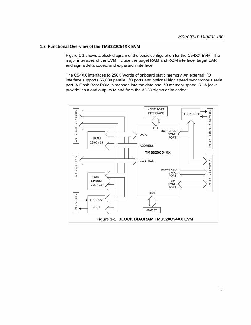
Figure 1-1 shows a block diagram of the basic configuration for the C54XX EVM. Themajor interfaces of the EVM include the target RAM and ROM interface, target UARTand sigma delta codec, and expansion interface.
The C54XX interfaces to 256K Words of onboard static memory. An external I/Ointerface supports 65,000 parallel I/O ports and optional high speed synchronous serialport. A Flash Boot ROM is mapped into the data and I/O memory space. RCA jacksprovide input and outputs to and from the AD50 sigma delta codec.
JTAG
DATA
ADDRESS
CONTROL
TMS320C54XX
JTAG P5
TL16C550
UART
FlashEPROM32K x 16
SRAM
256K x 16
ANALOG
EXPANSION
P2
I/O
EXPANSION
P1
ADDRESS/DATA
P3
CONTROL
P4
SERIAL
P7
Figure 1-1 BLOCK DIAGRAM TMS320C54XX EVM
SYNC
SYNC
SYNC
PORT
PORT
PORT
TLC320AD50
TDM
BUFFERED
BUFFERED
HOST PORTINTERFACE
HPI

Spectrum Digital, Inc
1-4 TMS320C54xx Evaluation Module Technical Reference
2-1
Chapter 2
Operation of the TMS320C54XX Evaluation Module
This chapter describes the operation of the TMS320C54XX EvaluationModule, the key interfaces and an outline of the circuit board.
Topic Page
2.0 The TMS320C54XX EVM Operation 2-32.1 The TMS320C54XX EVM Board 2-32.1.1 Power Connector 2-42.2 TMS320C54XX Memory Interface 2-42.2.1 Program Memory 2-62.2.2 Data Memory 2-102.2.3 I/O Space 2-122.3 Onboard UART 2-122.4 Oscillator Selection 2-122.5 Analog Interface 2-132.5.1 J2, Analog Input 2-132.5.2 J3, Analog Output 2-132.6 Expansion Bus 2-142.6.1 P1, I/O Expansion Connector 2-152.6.1.1 P1, I/O Expansion Connector for LC548, LC549, VC549 2-152.6.1.2 P1, I/O Expansion Connector for VC5402 2-162.6.1.3 P1, I/O Expansion Connector for VC5409/VC5410/ 2-17
VC54162.6.2 P2, Analog Expansion Connector 2-182.6.3 P3, Address/Data Expansion Connector 2-192.6.4 P4, Control Expansion Connector 2-202.6.4.1 P4, Control Expansion Connector for LC548, LC549, 2-20
VC549, VC54102.6.4.2 P4, Control Expansion Connector for VC5410 2-212.6.5 P6, Host Port Interface Expansion Connector 2-222.7 P7, JTAG Interface 2-232.8 Onboard Serial Interface 2-242.9 Boot Loading 2-25
Spectrum Digital, Inc
2-2 TMS320C54XX Evaluation Module Technical Reference
Topic Page
2.10 EVM320C54X Jumpers 2-272.10.1 Jumper Positions 2-282.10.2 JP1, UART Reset 2-282.10.3 JP2, Onboard UART CTS Routing 2-282.10.4 JP3, A15/A17 Select 2-282.10.5 JP4, AD50 AC/DC Coupling 2-292.10.6 JP5, Synchronous Port Routing 2-292.10.7 JP6, AD50 Reset 2-292.10.8 JP7, SYSCLK Option 2-302.10.9 JP8, AD50 Voltage Reference 2-302.10.10 JP9, DSP Core Voltage Select 2-312.10.11 JP10, Ready Routing 2-312.10.12 JP11, Onboard UART Interrupt Select 2-322.10.13 JP12, Voltage Select 2-322.10.14 JP13, Bootloader Enable/Disable 2-322.10.15 JP14, JP15, JP16 Oscillator Selection 2-332.11 LEDS 2-342.12 Resets 2-34

Spectrum Digital, Inc
2-3
2.0 The TMS320C54XX EVM Operation
This chapter describes the C54XX Evaluation module, key components, and howthey operate. It also provides information on the EVM’s various interfaces.The C54XXEVM consists of five major blocks of logic.
• C54XX external memory • Analog Interface• On board Serial I/O interface• Expansion interface• JTAG Interface
2.1 The TMS320C54XX EVM Board
The C54XX EVM is a 3U sized board which is powered by an external 5 Volt only powersupply. Figure 2-1 shows the layout of the C54XX EVM.
Figure 2-1, EVM320C54XX With Jumper Positions
JP1JP2
JP4
JP5
JP6
JP8
JP7
JP9 JP10 JP11 JP12 JP13-JP16
JP3

Spectrum Digital, Inc
2-4 TMS320C54XX Evaluation Module Technical Reference
2.1.1 Power Connector
The C54XX is powered by a 5 Volt only power supply which is available with themodule. The board requires 1 amp. The power is supplied via 2 millimeter jack J1. Ifexpansion boards are connected to the module a higher amperage power supply maybe necessary. The board also has a 3.3 and 2.5 volt regulator to provide power to thelower voltage components.
2.2 TMS320C54XX Memory Interface
The EVM includes 192k Words of on board program ram memory and 64k wordsof on board data ram memory, providing a total of 256k words of off chip static ram.The board also features two 32k flash ROMs for boot loading.
It is important to remember that internal memory has a higher precedence than theexternal memory. For more information on the memory in the device populated in yourEVM card please refer to Texas Instruments TMS320C54XX Users Guide. Futhermore,it is important to take into account that external memory is affected by wait-states. Waitstate generation for off-chip memory space (data, program, or I/O) is done with theSoftware Wait State Generation Register(SWWSR). To obtain one waitstate off-chipmemory bits in the SWWSR must be appropriately programmed. The board powers upwith 7 wait-states. The EVM board does not generate wait states via the ready signalfor external program and data memory accesses, only I/O accesses use the readysignal.
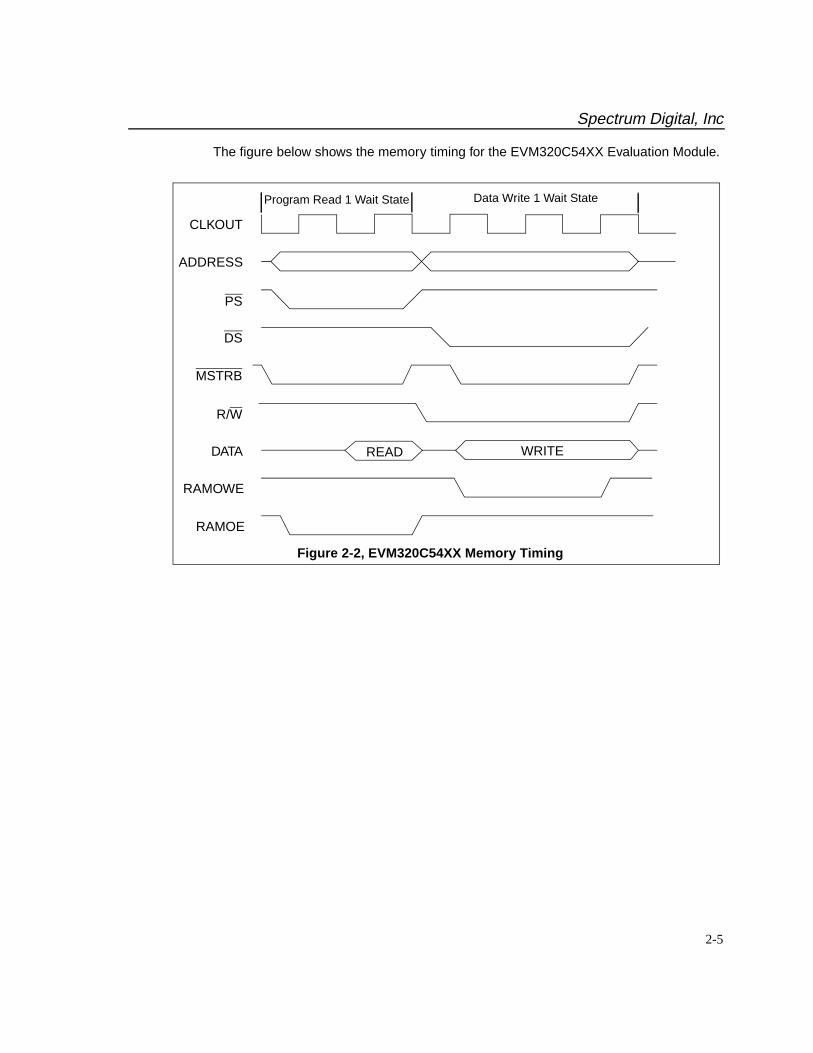
External memory decode is done via U14 a GAL20V8. The generic array device selectsthe RAM, FLASH ROM, or on board peripherals. The equations for the GAL areincluded in Appendix A. The figure below shows a one wait state program spacememory read followed by a data space memory write.
The external Flash ROM is mapped into the upper 32K words of data and I/O space forboot loading. Note that this memory requires multiple wait states. The main purpose ofthis memory is to allow for the boot loading of programs via the C54XX’s internal bootloader.
Spectrum Digital, Inc
2-5
The figure below shows the memory timing for the EVM320C54XX Evaluation Module.
CLKOUT
ADDRESS
Figure 2-2, EVM320C54XX Memory Timing
READ WRITE
PS
DS
MSTRB
R/W
DATA
RAMOWE
RAMOE
Program Read 1 Wait State Data Write 1 Wait State

Spectrum Digital, Inc
2-6 TMS320C54XX Evaluation Module Technical Reference
2.2.1 Program Memory
There are two configurations for program memory. The selection of these configurations is done by the 54X’s OVLY bit. When in OVLY mode, addresses0x0000 - 0x8000 are internal for every page. In this mode, there are five (5) 32K wordpages of external program RAM and one (1) 32K word page of internal RAM. When inlinear mode program memory is mapped to external RAM. Shown below are the twoprogram memory configurations. The following three figures are for the C548 andC549 processors, C5410 processor, and the C5402 respectively.
Hex
Overlay Mode, OVLY = 1Linear Mode, OVLY = 0
Hex
0x000000
0x00007F
0x000080
0x007FFF
0x00FF80
0x00FFFF
0x010000
0x027FFF
0x008000
0x00FF7F
0x001FFF
0x002000
0x028000
0x05FFFF
External
External
External
External
External
External
Interrupts External
Reserved
DARAM
SARAM
Page 0
Page 0
External RAM
Interrupts
0x000000
0x00007F
0x000080
0x001FFF
0x002000
0x007FFF
0x00FFFF
0x00FF80
0x008000
0x00FF7F
RAM
RAM
RAM
RAM
RAM
RAM
Figure 2-3A, EVM320C548/549/5409 Program Space
Page 1
Page 2
Page 3
Page 4
External RAM
External RAM
External RAM
0x018000
0x028000
0x038000
0x048000
0x01FFFF
0x02FFFF
0x03FFFF
0x04FFFF
RAM Images
0x37FFFF
0x060000
* Jumper JP13 in 2-3 position
† Jumper JP13 in 1-2 position
0x05FFFF
0x058000
External Page
0x37FFFF
0x060000
External RAM
RAM Images
External RAM

Spectrum Digital, Inc
2-7
Note that in Microcontroller Mode, MP/MC pin=0, the on chip boot loader resides inhigh page 0 address space. These addresses are 0xC000 to 0xFFFF on the C549and C5410, from 0xF000 to 0xFFFF on the C5402 processor, and from 0xF800 to0xFFFF on the C548.
Hex
Overlay Mode, OVLY = 1Linear Mode, OVLY = 0
Hex
0x000000
0x00007F
0x000080
0x007FFF
0x00FF80
0x00FFFF
0x010000
0x027FFF
0x008000
0x00FF7F
0x001FFF
0x002000
0x028000
0x05FFFF
External
External
External
External
External
External
Interrupts External
Reserved
DARAM
SARAM
Page 0
Page 0
External RAM
Interrupts
0x000000
0x00007F
0x000080
0x001FFF
0x002000
0x007FFF
0x00FFFF
0x00FF80
0x008000
0x00FF7F
RAM
RAM
RAM
RAM
RAM
RAM
Figure 2-3B, EVM320VC5410 Program Space
Page 1
Page 3
Page 4
Internal SARAM2
External RAM
0x018000
0x028000
0x038000
0x048000
0x01FFFF
0x02FFFF
0x03FFFF
0x04FFFF
RAM Images
0x37FFFF
0x060000
* Jumper JP13 in 2-3 position
† Jumper JP13 in 1-2 position
0x05FFFF
0x058000
External
0x37FFFF
0x060000
External RAM
RAM Images
Internal
Internal
Page 2
External RAM
External RAM
Note: JP13 maps A15 or A15 RAM’s A17 is default.

Spectrum Digital, Inc
2-8 TMS320C54XX Evaluation Module Technical Reference
In Microcontroller Mode, MP/MC pin=0, the on chip boot loader resides in high page0 address space. These addresses are 0xC000 to 0xFFFF on the C549 and C5410,from 0xF000 to 0xFFFF on the C5402 processor, and from 0xF800 to 0xFFFF on theC548.
Hex
Overlay Mode, OVLY = 1Linear Mode, OVLY = 0
Hex
0x000000
0x00007F
0x000080
0x007FFF
0x00FF80
0x00FFFF
0x010000
0x027FFF
0x008000
0x00FF7F
0x001FFF
0x002000
0x028000
0x05FFFF
External
External
External
External
External
External
Interrupts External
Reserved
DARAM
Page 0
Page 0
External RAM
Interrupts
0x000000
0x00007F
0x000080
0x003FFF
0x004000
0x007FFF
0x00FFFF
0x00FF80
0x008000
0x00FF7F
RAM
RAM
RAM
RAM
RAM
RAM
Figure 2-3C, EVM320VC5402 Program Space
Page 1
Page 3
Page 4
Internal SARAM2
External RAM
0x018000
0x028000
0x038000
0x048000
0x01FFFF
0x02FFFF
0x03FFFF
0x04FFFF
RAM Images
0x37FFFF
0x060000
* Jumper JP13 in 2-3 position
† Jumper JP13 in 1-2 position
0x05FFFF
0x058000
External
0x37FFFF
0x060000
External RAM
RAM Images
Internal
External
Page 2
External RAM
External RAM
Note: JP13 maps A15 or A15 RAM’s A17 is default.

Spectrum Digital, Inc
2-9
Hex
Overlay Mode, OVLY = 1Linear Mode, OVLY = 0
Hex
0x000000
0x00007F
0x000080
0x00FF7F
0x010000
0x017FFF
0x018000
0x01FFFF
0x00FF80
0x00FFFF
0x007FFF
0x008000
0x020000
0x027FFF
External
External RAM
External MP/MC=1
External
External RAM
Reserved
DARAM
Page 0
Page 1
0x000000
0x00007F
0x000080
0x007FFF
0x008000
0x00BFFF
0x01FFFF
0x018000
0x00C000
0x00FFFF
Reserved
Figure 2-3D, EVM320VC5416 Program Space
Page 2
Page 4
Page 5
External RAM
0x028000
0x038000
0x048000
0x058000
0x02FFFF
0x03FFFF
0x04FFFF
0x05FFFF
0x02FFFF
0x028000
† Jumper JP13 in 1-2 position
0x06FFFF
0x068000
External
0x3FFFFF
0x080000
External RAM
Internal
* External RAM
Page 3
If MP/MC=1, pages 4-7 are images of pages 0-3
Page 0
* External MP/MC=1
Internal ROM MP/MC=0
* External MP/MC=1
Internal DARAM MP/MC=0
Internal DARAM MP/MC=0
Internal DARAM MP/MC=0
* External MP/MC=1
* External MP/MC=1
Page 6
Page 7
External RAM
External RAM0x07FFFF
0x078000
External
Page 7
Page 6
Page 5
Page 4
Page 3
Page 3
Page 2
Page 2
Page 1
Page 1
Page 0
Page 0Interrupts
External
Internal MP/MC=0
External
External MP/MC=1Internal SRAM MP/MC=0
Image
Image External RAM
Image External RAM
Image External RAM
Image External RAM
Internal MP/MC=1External RAM MP/MC=0
0x080000
0x3FFFFF
0x030000
0x037FFF
0x038000
0x03FFFF
0x048000
0x04FFFF
0x058000
0x05FFFF
0x068000
0x06FFFF
0x078000
0x07FFFF
†† Image of page 4
†† Page 4 is mirror image of page 0when MP/MC=0
Spectrum Digital, Inc
2-10 TMS320C54XX Evaluation Module Technical Reference
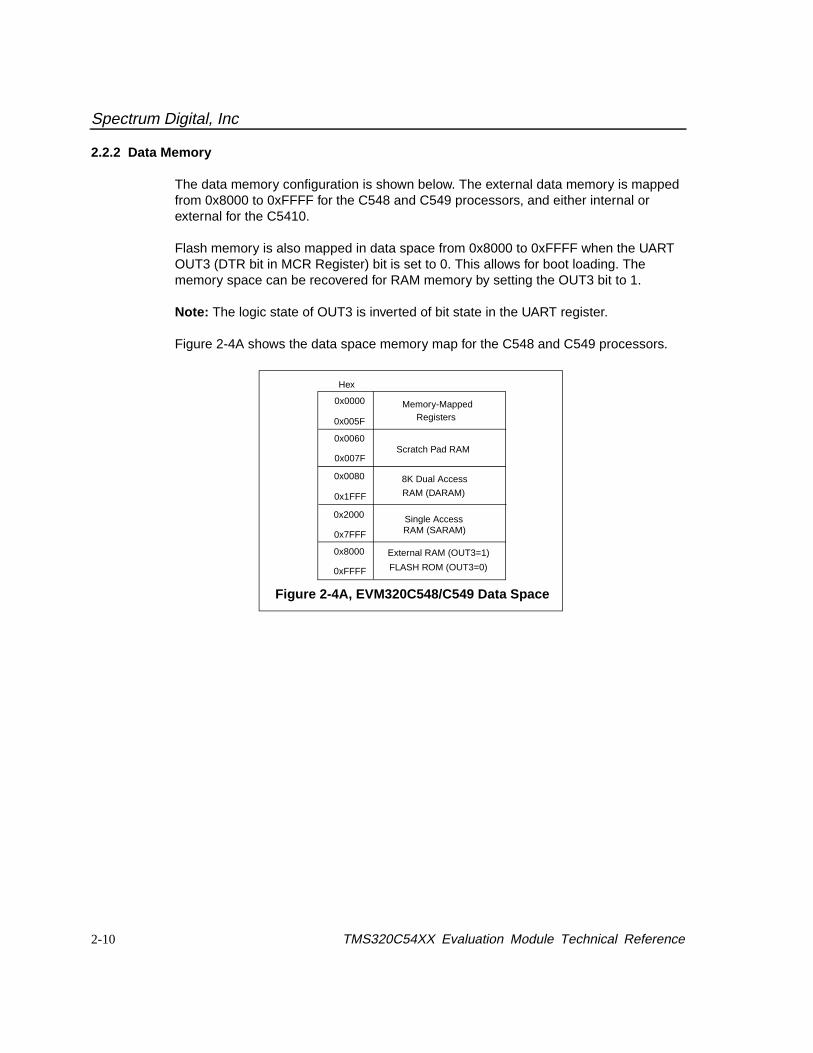
2.2.2 Data Memory
The data memory configuration is shown below. The external data memory is mappedfrom 0x8000 to 0xFFFF for the C548 and C549 processors, and either internal orexternal for the C5410.
Flash memory is also mapped in data space from 0x8000 to 0xFFFF when the UARTOUT3 (DTR bit in MCR Register) bit is set to 0. This allows for boot loading. Thememory space can be recovered for RAM memory by setting the OUT3 bit to 1.
Note: The logic state of OUT3 is inverted of bit state in the UART register.
Figure 2-4A shows the data space memory map for the C548 and C549 processors.
Hex
0x0000
0x005F
0x0060
0x007F
0x0080
0x1FFF
0x2000
0x7FFF
0x8000
0xFFFF
Memory-MappedRegisters
Scratch Pad RAM
8K Dual Access
RAM (DARAM)
Single AccessRAM (SARAM)
FLASH ROM (OUT3=0)
External RAM (OUT3=1)
Figure 2-4A, EVM320C548/C549 Data Space

Spectrum Digital, Inc
2-11
Figure 2-4B shows the data space memory map for the VC5410 and VC5416 DSP.
Figure 2-4C shows the data space memory map for the VC5402 DSP.
Hex
0x0000
0x005F
0x0060
0x007F
0x0080
0x1FFF
0x2000
0x7FFF
0x8000
0xFFFF
Memory-MappedRegisters
Scratch Pad RAM
8K Dual Access
RAM (DARAM)
Single AccessRAM (SARAM)
FLASH ROM (OUT3=0, DROM=0)
External RAM (OUT3=1, DROM=0)
Figure 2-4B, EVM320VC5410, VC5416 Data Space
Internal SARAM2 (OUT3=X, DROM=1)
Hex
0x0000
0x005F
0x0060
0x007F
0x0080
0x3FFF
0x4000
0x7FFF
0x8000
0xFFFF
Memory-MappedRegisters
Scratch Pad RAM
8K Dual Access
RAM (DARAM)
External RAM
FLASH ROM (OUT3=0, DROM=0)
External RAM (OUT3=1, DROM=0)
Figure 2-4C, EVM320VC5402 Data Space
Internal SARAM2 (OUT3=X, DROM=1)
Spectrum Digital, Inc
2-12 TMS320C54XX Evaluation Module Technical Reference
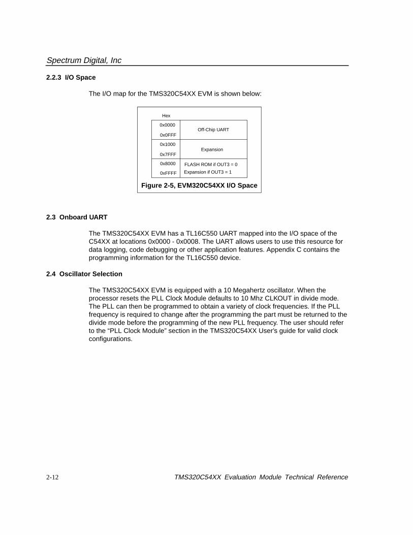
2.2.3 I/O Space
The I/O map for the TMS320C54XX EVM is shown below:
2.3 Onboard UART
The TMS320C54XX EVM has a TL16C550 UART mapped into the I/O space of theC54XX at locations 0x0000 - 0x0008. The UART allows users to use this resource fordata logging, code debugging or other application features. Appendix C contains theprogramming information for the TL16C550 device.
2.4 Oscillator Selection
The TMS320C54XX EVM is equipped with a 10 Megahertz oscillator. When theprocessor resets the PLL Clock Module defaults to 10 Mhz CLKOUT in divide mode.The PLL can then be programmed to obtain a variety of clock frequencies. If the PLLfrequency is required to change after the programming the part must be returned to thedivide mode before the programming of the new PLL frequency. The user should referto the “PLL Clock Module” section in the TMS320C54XX User’s guide for valid clockconfigurations.
Hex
0x0000
0x0FFF
0x1000
0x7FFF
0x8000
0xFFFF
Off-Chip UART
Expansion
FLASH ROM if OUT3 = 0
Expansion if OUT3 = 1
Figure 2-5, EVM320C54XX I/O Space
Spectrum Digital, Inc
2-13
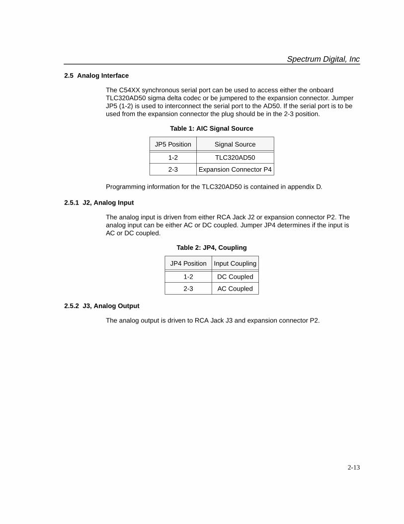
2.5 Analog Interface
The C54XX synchronous serial port can be used to access either the onboardTLC320AD50 sigma delta codec or be jumpered to the expansion connector. JumperJP5 (1-2) is used to interconnect the serial port to the AD50. If the serial port is to beused from the expansion connector the plug should be in the 2-3 position.
Programming information for the TLC320AD50 is contained in appendix D.
2.5.1 J2, Analog Input
The analog input is driven from either RCA Jack J2 or expansion connector P2. Theanalog input can be either AC or DC coupled. Jumper JP4 determines if the input isAC or DC coupled.
2.5.2 J3, Analog Output
The analog output is driven to RCA Jack J3 and expansion connector P2.
Table 1: AIC Signal Source
JP5 Position Signal Source
1-2 TLC320AD50
2-3 Expansion Connector P4
Table 2: JP4, Coupling
JP4 Position Input Coupling
1-2 DC Coupled
2-3 AC Coupled

Spectrum Digital, Inc
2-14 TMS320C54XX Evaluation Module Technical Reference
2.6 Expansion Bus
The TMS320C54XX EVM has an expansion bus which brings out all of the signals fromthe DSP. This expansion bus allows the user to design custom circuitry to be used withhis application without having to design a CPU card. In addition this interface is used bySpectrum Digital for all of its add-on modules.
This expansion bus is divided into 5 double row header connectors. This sectioncontains the signal definitions and pin numbers for each of the connectors.
Table 3: Expansion Bus Connectors
Connector Function
P1 I/O Expansion
P2 Analog Expansion
P3 Address/Data
P4 Control
P6 Host Port Interface
Spectrum Digital, Inc
2-15
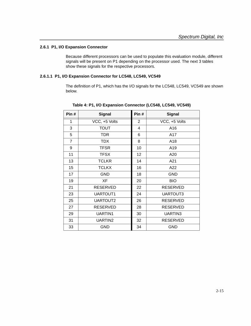
2.6.1 P1, I/O Expansion Connector
Because different processors can be used to populate this evaluation module, differentsignals will be present on P1 depending on the processor used. The next 3 tablesshow these signals for the respective processors.
2.6.1.1 P1, I/O Expansion Connector for LC548, LC549, VC549
The definition of P1, which has the I/O signals for the LC548, LC549, VC549 are shownbelow.
Table 4: P1, I/O Expansion Connector (LC548, LC549, VC549)
Pin # Signal Pin # Signal
1 VCC, +5 Volts 2 VCC, +5 Volts
3 TOUT 4 A16
5 TDR 6 A17
7 TDX 8 A18
9 TFSR 10 A19
11 TFSX 12 A20
13 TCLKR 14 A21
15 TCLKX 16 A22
17 GND 18 GND
19 XF 20 BIO
21 RESERVED 22 RESERVED
23 UARTOUT1 24 UARTOUT3
25 UARTOUT2 26 RESERVED
27 RESERVED 28 RESERVED
29 UARTIN1 30 UARTIN3
31 UARTIN2 32 RESERVED
33 GND 34 GND
Spectrum Digital, Inc
2-16 TMS320C54XX Evaluation Module Technical Reference
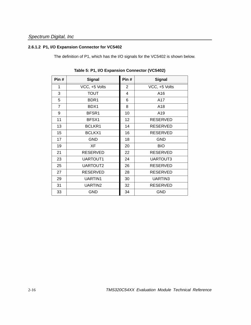
2.6.1.2 P1, I/O Expansion Connector for VC5402
The definition of P1, which has the I/O signals for the VC5402 is shown below.
Table 5: P1, I/O Expansion Connector (VC5402)
Pin # Signal Pin # Signal
1 VCC, +5 Volts 2 VCC, +5 Volts
3 TOUT 4 A16
5 BDR1 6 A17
7 BDX1 8 A18
9 BFSR1 10 A19
11 BFSX1 12 RESERVED
13 BCLKR1 14 RESERVED
15 BCLKX1 16 RESERVED
17 GND 18 GND
19 XF 20 BIO
21 RESERVED 22 RESERVED
23 UARTOUT1 24 UARTOUT3
25 UARTOUT2 26 RESERVED
27 RESERVED 28 RESERVED
29 UARTIN1 30 UARTIN3
31 UARTIN2 32 RESERVED
33 GND 34 GND

Spectrum Digital, Inc
2-17
2.6.1.3 P1, I/O Expansion Connector for VC5409/VC5410, VC5416
The definition of P1, which has the I/O signals for the VC5409, VC5410, and VC5416are shown below.
Table 6: P1, I/O Expansion Connector (VC5409/VC5410/VC5416)
Pin # Signal Pin # Signal
1 VCC, +5 Volts 2 VCC, +5 Volts
3 TOUT 4 A16
5 BDR2 6 A17
7 BDX2 8 A18
9 BFSR2 10 A19
11 BFSX2 12 A20
13 BCLKR2 14 A21
15 BCLKX2 16 A22
17 GND 18 GND
19 XF 20 BIO
21 RESERVED 22 RESERVED
23 UARTOUT1 24 UARTOUT3
25 UARTOUT2 26 RESERVED
27 RESERVED 28 RESERVED
29 UARTIN1 30 UARTIN3
31 UARTIN2 32 RESERVED
33 GND 34 GND
Spectrum Digital, Inc
2-18 TMS320C54XX Evaluation Module Technical Reference
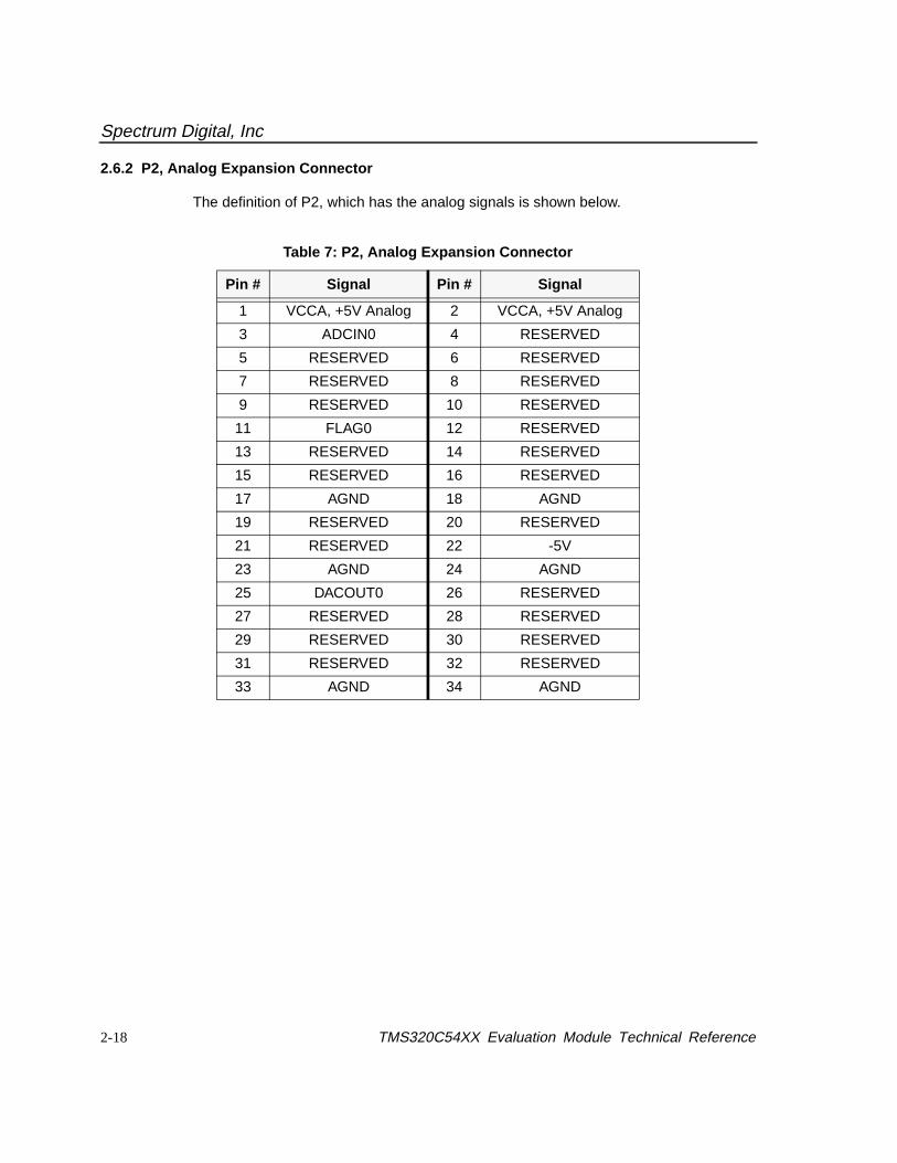
2.6.2 P2, Analog Expansion Connector
The definition of P2, which has the analog signals is shown below.
Table 7: P2, Analog Expansion Connector
Pin # Signal Pin # Signal
1 VCCA, +5V Analog 2 VCCA, +5V Analog
3 ADCIN0 4 RESERVED
5 RESERVED 6 RESERVED
7 RESERVED 8 RESERVED
9 RESERVED 10 RESERVED
11 FLAG0 12 RESERVED
13 RESERVED 14 RESERVED
15 RESERVED 16 RESERVED
17 AGND 18 AGND
19 RESERVED 20 RESERVED
21 RESERVED 22 -5V
23 AGND 24 AGND
25 DACOUT0 26 RESERVED
27 RESERVED 28 RESERVED
29 RESERVED 30 RESERVED
31 RESERVED 32 RESERVED
33 AGND 34 AGND

Spectrum Digital, Inc
2-19
2.6.3 P3, Address/data Expansion Connector
The definition of P3, which has the address and data signals is shown below.
Table 8: P3, Address/Data Expansion Connector
Pin # Signal Pin # Signal
1 A0 2 A1
3 A2 4 A3
5 A4 6 A5
7 A6 8 A7
9 A8 10 A9
11 A10 12 A11
13 A12 14 A13
15 A14 16 A15
17 GND 18 GND
19 D0 20 D1
21 D2 22 D3
23 D4 24 D5
25 D6 26 D7
27 D8 28 D9
29 D10 30 D11
31 D12 32 D13
33 D14 34 D15
Spectrum Digital, Inc
2-20 TMS320C54XX Evaluation Module Technical Reference
2.6.4 P4, Control Expansion Connector
Because different processors can be used to populate this evaluation module, differentsignals will be present on P4 depending on the processor used. The next 2 tablesshow these signals for the respective processors.
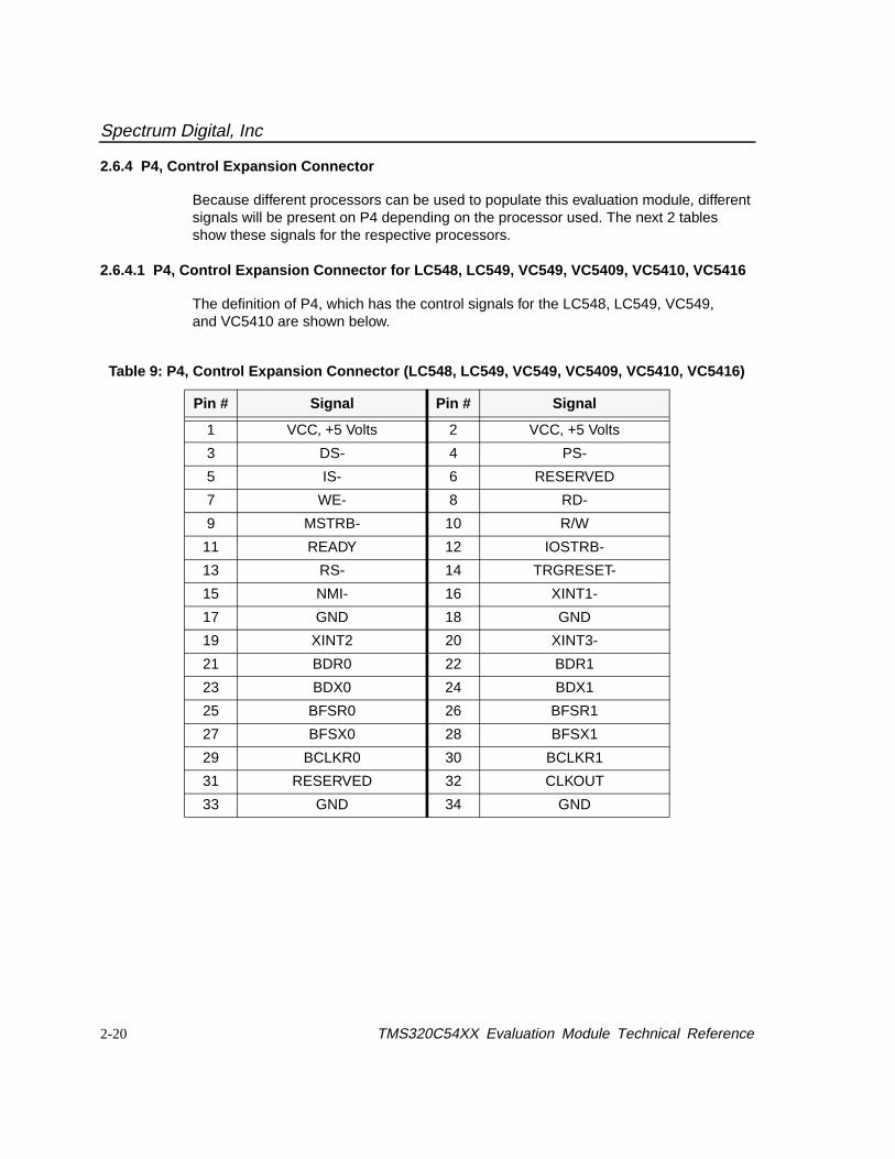
2.6.4.1 P4, Control Expansion Connector for LC548, LC549, VC549, VC5409, VC5410, VC5416
The definition of P4, which has the control signals for the LC548, LC549, VC549,and VC5410 are shown below.
Table 9: P4, Control Expansion Connector (LC548, LC549, VC549, VC5409, VC5410, VC5416)
Pin # Signal Pin # Signal
1 VCC, +5 Volts 2 VCC, +5 Volts
3 DS- 4 PS-
5 IS- 6 RESERVED
7 WE- 8 RD-
9 MSTRB- 10 R/W
11 READY 12 IOSTRB-
13 RS- 14 TRGRESET-
15 NMI- 16 XINT1-
17 GND 18 GND
19 XINT2 20 XINT3-
21 BDR0 22 BDR1
23 BDX0 24 BDX1
25 BFSR0 26 BFSR1
27 BFSX0 28 BFSX1
29 BCLKR0 30 BCLKR1
31 RESERVED 32 CLKOUT
33 GND 34 GND
Spectrum Digital, Inc
2-21
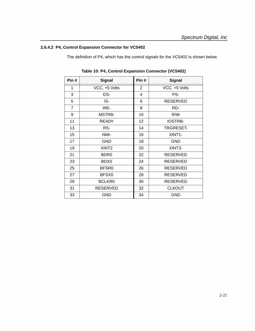
2.6.4.2 P4, Control Expansion Connector for VC5402
The definition of P4, which has the control signals for the VC5402 is shown below.
Table 10: P4, Control Expansion Connector (VC5402)
Pin # Signal Pin # Signal
1 VCC, +5 Volts 2 VCC, +5 Volts
3 DS- 4 PS-
5 IS- 6 RESERVED
7 WE- 8 RD-
9 MSTRB- 10 R/W
11 READY 12 IOSTRB-
13 RS- 14 TRGRESET-
15 NMI- 16 XINT1-
17 GND 18 GND
19 XINT2 20 XINT3-
21 BDR0 22 RESERVED
23 BDX0 24 RESERVED
25 BFSR0 26 RESERVED
27 BFSX0 28 RESERVED
29 BCLKR0 30 RESERVED
31 RESERVED 32 CLKOUT
33 GND 34 GND

Spectrum Digital, Inc
2-22 TMS320C54XX Evaluation Module Technical Reference
2.6.5 P6, Host Port Interface Expansion Connector
The definition of P6, which has the Host Port Interface signals is shown below.
Table 11: P6, Host Port Interface
Pin # Signal Pin # Signal
1 HD0 2 HD1
3 HD2 4 HD3
5 HD4 6 HD5
7 HD6 8 HD7
9 RESERVED 10 RESERVED
11 RESERVED 12 RESERVED
13 RESERVED 14 RESERVED
15 RESERVED 16 RESERVED
17 GND 18 GND
19 HCS 20 HDCNTL0
21 RESERVED 22 HDCNTL1
23 HRW 24 HDS2
25 HRDY 26 HDS1
27 HINT 28 HAS
29 HBIL 30 RESERVED
31 RESERVED 32 RESERVED
33 GND 34 GND

Spectrum Digital, Inc
2-23
2.7 P7, JTAG Interface.
The TMS320C54XX Evaluation Module is supplied with a 14 pin header interface, P7.This is the standard interface used by JTAG emulators to interface to TexasInstruments DSPs. The pinout for the connector is shown figure 2-6 below:
1 23 4
5 67 89 1011 1213 14
TMSTDI
PD (+5V)TDO
TCK-RET
TCKEMU0
TRST-GNDno pin (key)GNDGND
GNDEMU1
Header Dimensions
Pin-to-Pin spacing, 0.100 in. (X,Y)Pin width, 0.025-in. square post
Pin length, 0.235-in. nominal
Figure 2-6, JTAG INTERFACE

Spectrum Digital, Inc
2-24 TMS320C54XX Evaluation Module Technical Reference
2.8 Onboard Serial Interface
The EVM320C54XX has a TL16C550 UART (U8) which provides a an additional serialinterface. This UART is mapped into I/O space at locations 0x0000 to 0x0008. Thisdevice allows users to use this resource for data logging, code debugging and otherapplications. The software wait state generator should be set to 3-7 wait states beforeaccessing the UART. The UART interface GAL, U22, generates the necessary waitstates to complete the interface cycle.
This UART is brought out to connector P5 on the EVM320C54XX. Connector P5 is aDB9 female connector. The pin positions for the P5 connector as viewed from the edgeof the EVM320C54XX.
The pin numbers and their corresponding signals are shown in the table below:
* Jumper JP2 can be used to configure pin 4 to pin 7 on P5. This allows for normal handshaking. The jumper settings are shown in the table below:
Table 12: P5, RS232 Pinout
Pin # PC (female) SD EVM
2 Rx, input Tx, output
3 Tx, output Rx, input
4 DTR, output Reset/CTS, input*
5 GND GND
8 CTS, input RTS, output
Table 13: JP2 Settings
JP2 Position CTS Routing
1-2 P5 pin 4 used on CTS input
2-3 P5 pin 7 used on CTS input
9
5 4 3 2 1
8 7 6
Figure 2-7, P5, DB9 Female Connector

Spectrum Digital, Inc
2-25
The UART can be jumpered via JP11 to generate different interrupt levels. The type ofinterrupt is shown in the table below:
2.9 Boot Loading
The EVM320C54xx is equipped with 32K words of flash ROM for parallel boot loading. Thisfeature does not disallow the ability to boot from the HPI or serial port, but is intended to allowa convenient method of implementing embedded code on the C54XX evaluation module.
The flash ROM on the evaluation module is mapped in data space and I/O space from0x8000 to 0xFFFF when the module is reset. If the module is in microcomputer mode(MP/MC pin = 0) the boot loader will be executed.
To boot load from flash memory the data must be built in the proper format for the boot loader.Upon execution of the boot loader in parallel mode the on chip boot loader reads the I/Ospace and/or the data space at 0xFFFF to find the boot loader source address. Theappropriate value for the source address boot loading is 0x8000, the flash ROM baseaddress in data space. Since the flash on the evaluation module is word wide we will use the16 bit parallel load mode in our example.
After the boot loader extracts the source address from the location specified (0xFFFF). Theboot loader recognition word (0x10AA) must be located at this address (0x8000 in ourexample) as shown in table 12.
In our example one section of 0x4000 words will be loaded via the boot loader. Since the partwill be in overlay mode on booting our target program space map will be one shown in figure2-7 in internal C54XX memory.
Table 14: Onboard UART Interrupt Selection
JP11 Position Interrupt Level
1-2 NMI
2-3 INT1

Spectrum Digital, Inc
2-26 TMS320C54XX Evaluation Module Technical Reference
In our example one section is loaded. However, if multiple sections are used they are tackedonto the first section in the same format as the first section(0x8005 to 0xc008). Of course, thesize of each section is independent, as long as the total size of all the sections is less than32K words. For more information on boot loading options please refer to the C548/C549 bootloading document available from Texas Instruments
Table 15: Sample Boot Load Format Stored In Flash ROM
Data Space Address
Data Space Data
Function
0xFFFF 0x8000 Source Address
... 0x0000 Zero Fill
0xC009 0x0000 ...
0xC008 0xF495(NOP) Last Op Code, 1st Section
0xF495(NOP)
0x8009 1st Op Code, 1st Section
0x8007 0x4000 Destination Address
0x8006 0x0000 Destination of 1st XPC
0x8005 0x4000 Size of 1st Section
0x8004 0x7F80 Entry Point
0x8003 0x0000 Entry XPC
0x8002 0x8802 BSCR Value
0x8001 0x7FFF SWWR Value
0x8000 0x10AA Recognition byte 16 bit mode
0x7FFF
Interrupt Vectors
1st Op code
0x7F80
0x4000
0xF073
NOP
NOP
Figure 2-8, Boot Load Example Internal Memory
0x4000
0x7F7F
0x7F7E
B 0x4000Last Op Code1st Section
CommentsProgram Address Data

Spectrum Digital, Inc
2-27
2.10 EVM320C54X Jumpers
The EVM320C54X has 14 jumpers which determine how features on the EVM areutilized. The table below lists the jumpers and their function. The followingsections describe the use of each jumper.
Each jumper on the TMS320C54XX EVM is a 1x3 jumper except for jumper. Each 1x3jumper must have the selection 1-2 or 2-3. The #2 pin is the center pin. The #1 pin hasa square solder pad and can be seen from the solder side of the printed circuit board.This pin is usually marked with a ‘1’ on the boards silkscreen. A top view of both typesof jumpers is shown below:
Table 16: EVM320C54X Jumpers
Jumper # Size Function
JP1 1 x 3 UART Reset
JP2 1 x 3 UART CTS Routing
JP3 1 x 3 A15/A17 Select
JP4 1 x 3 AD50 AC/DC Coupling
JP5 1 x 3 Synchronous Port Routing
JP6 1 x 3 AD50 Reset
JP7 1 x 3 SYSCLK Option
JP8 1 x 3 AD50 Reference Voltage
JP9 1 x 3 DSP Core Voltage Select
JP10 1 x 3 READY Option
JP11 1 x 3 Onboard UART Interrupt Select
JP12 1 x 2 Voltage select (1.8v/2.5v/3.3v) Default = 1.8 volt, factory installed
JP13 1 x 3 Bootloader Enable
JP14, JP15, JP16 1 x 3 Oscillator Mode Select
31 2
Figure 2-9 1x3 Jumper Layout
WARNING!
be installed in either the 1-2 or 2-3 positionUnless noted otherwise, all 1x3 jumpers must
Spectrum Digital, Inc
2-28 TMS320C54XX Evaluation Module Technical Reference
2.10.1 Jumper Positions
The figure 2-1 shows the locations of the jumpers on the EVM320C54XX EVM.
2.10.2 JP1, UART Reset
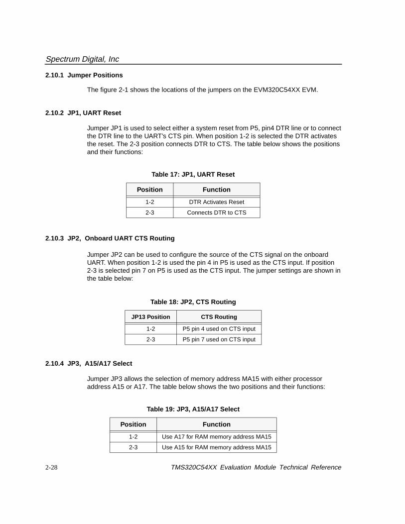
Jumper JP1 is used to select either a system reset from P5, pin4 DTR line or to connectthe DTR line to the UART’s CTS pin. When position 1-2 is selected the DTR activatesthe reset. The 2-3 position connects DTR to CTS. The table below shows the positionsand their functions:
2.10.3 JP2, Onboard UART CTS Routing
Jumper JP2 can be used to configure the source of the CTS signal on the onboardUART. When position 1-2 is used the pin 4 in P5 is used as the CTS input. If position2-3 is selected pin 7 on P5 is used as the CTS input. The jumper settings are shown inthe table below:
2.10.4 JP3, A15/A17 Select
Jumper JP3 allows the selection of memory address MA15 with either processoraddress A15 or A17. The table below shows the two positions and their functions:
Table 17: JP1, UART Reset
Position Function
1-2 DTR Activates Reset
2-3 Connects DTR to CTS
Table 18: JP2, CTS Routing
JP13 Position CTS Routing
1-2 P5 pin 4 used on CTS input
2-3 P5 pin 7 used on CTS input
Table 19: JP3, A15/A17 Select
Position Function
1-2 Use A17 for RAM memory address MA15
2-3 Use A15 for RAM memory address MA15

Spectrum Digital, Inc
2-29
2.10.5 JP4, AD50 AC/DC Coupling
Jumper JP4 is used to select the coupling for the analog input. If position 1-2 is selectedthe coupling is DC. The 2-3 selection will provide AC coupling.
2.10.6 JP5, Synchronous Port Routing
Jumper JP5 is used to connect the source of data for the synchronous serial port on theC54XX. By selecting position 1-2 the synchronous serial port is connected to theTLC320AD50 AIC. Position 2-3 connects the serial port to the expansion connector P4he table below shows the positions and their functions:
2.10.7 JP6, AD50 Reset
The AD50 Codec can be reset either by the system reset or a user option. Position 1-2allows the AD50 to be reset by the system reset. In position 2-3 the AD50 is resetfrom a user defined pin on the DSP. The table below shows the positions and theirfunctions:
Table 20: JP4, AC/DC Coupling
Position Function
1-2 DC Coupled
2-3 AC Coupled
Table 21: JP5, Synchronous Port Routing
Position Function
1-2 TLC320AD50
2-3 Expansion Connector P4
Table 22: JP6, AD50 Reset
Position Function
1-2 System Reset Activates AD50 Reset
2-3 User option

Spectrum Digital, Inc
2-30 TMS320C54XX Evaluation Module Technical Reference
2.10.8 JP7, SYSCLK Option
Jumper JP7 allows the selection of either the rising edge or falling edge of CLKOUT togenerate READY for UART operations. As processor frequencies increase it will benecessary to pipeline the READY signal. This jumper provides for these requirements.The table below shows the two positions and their functions:
2.10.9 JP8, AD50 Reference Voltage
The AD50 AIC can supply an internal reference voltage, however for compatibility withprevious versions of the C54xx with the AD50, an external voltage reference issupplied. Jumper JP8 allows the selection of using the external reference or internalreference. When position 1-2 is selected the external reference is used. If the 2-3position is selected the internal reference is used. These selections are shown in thetable below.
Table 23: JP7, SYSCLK Option
Position Function
1-2 Use Inverted CLKOUT for U20 GAL Clock
2-3 Use CLKOUT for U20 GAL Clock
Table 24: JP8, AD50 Reference Voltage
Position Function
1-2 External reference
2-3 Internal reference

Spectrum Digital, Inc
2-31
2.10.10 JP9, DSP Core Voltage Select
Jumper JP9 is used to control the voltage to the core of the C54x DSP. If you are notsure of the core voltage refer to a data sheet prior to changing this jumper. The tablebelow shows the setting and the corresponding voltages.
This jumper is set to the appropriate position before shipment.
* resistor values set differently at factory for VC5416.
2.10.11 JP10, Ready Routing
READY to the C54XX device from the GAL U20 can be deactivated if necessary. Ofcourse this prevents use of the onboard UART. In normal mode (position 1-2) externalREADY from the I/O connector is routed through GAL U20. When JP10 is in the 2-3position the READY signal is routed directly from the expansion connector to theC54XX device. The table below shows the positions and their functions:
Table 25: JP9, DSP Core Voltage Select
Position Core Voltage Device JP12
1-2 3.3 Volts LC548, LC549 Not installed
2-3 2.5 Volts VC549,VC5410 Not installed
2-3 1.8 Volts VC5402,VC5409,VC5416 Installed
2-3* 1.5 Volts VC5416 Not Installed
Table 26: JP10, READY Routing
JP5 Position Function
1-2 READY from GAL U20
2-3 READY directly from I/O expansion connector
WARNING!
Setting this jumper incorrectlycan damage to the DSP device
Spectrum Digital, Inc
2-32 TMS320C54XX Evaluation Module Technical Reference
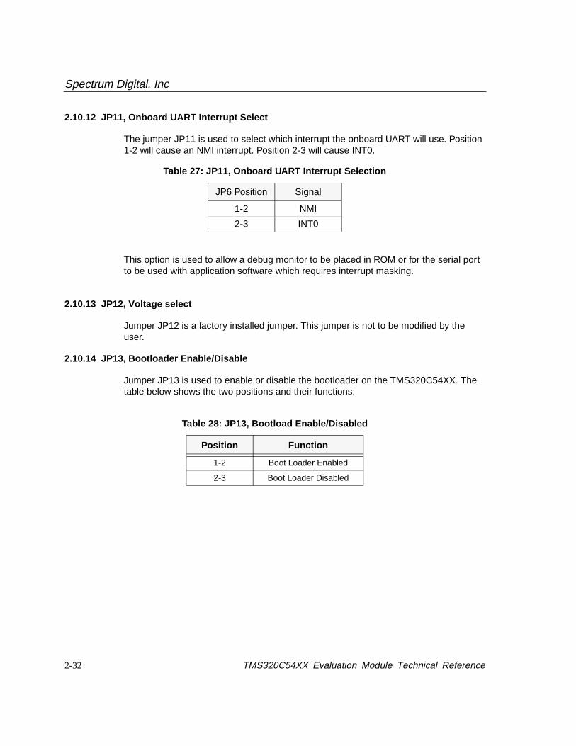
2.10.12 JP11, Onboard UART Interrupt Select
The jumper JP11 is used to select which interrupt the onboard UART will use. Position1-2 will cause an NMI interrupt. Position 2-3 will cause INT0.
This option is used to allow a debug monitor to be placed in ROM or for the serial portto be used with application software which requires interrupt masking.
2.10.13 JP12, Voltage select
Jumper JP12 is a factory installed jumper. This jumper is not to be modified by theuser.
2.10.14 JP13, Bootloader Enable/Disable
Jumper JP13 is used to enable or disable the bootloader on the TMS320C54XX. Thetable below shows the two positions and their functions:
Table 27: JP11, Onboard UART Interrupt Selection
JP6 Position Signal
1-2 NMI
2-3 INT0
Table 28: JP13, Bootload Enable/Disabled
Position Function
1-2 Boot Loader Enabled
2-3 Boot Loader Disabled
Spectrum Digital, Inc
2-33
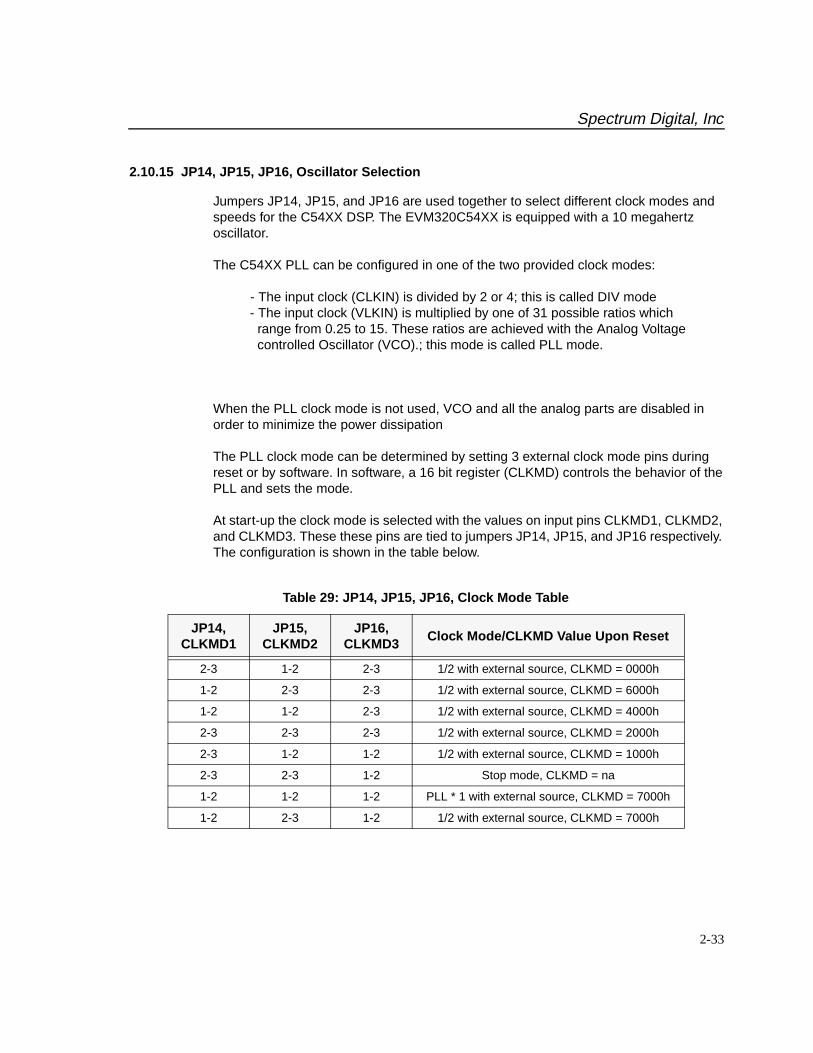
2.10.15 JP14, JP15, JP16, Oscillator Selection
Jumpers JP14, JP15, and JP16 are used together to select different clock modes andspeeds for the C54XX DSP. The EVM320C54XX is equipped with a 10 megahertzoscillator.
The C54XX PLL can be configured in one of the two provided clock modes:
- The input clock (CLKIN) is divided by 2 or 4; this is called DIV mode - The input clock (VLKIN) is multiplied by one of 31 possible ratios which range from 0.25 to 15. These ratios are achieved with the Analog Voltage controlled Oscillator (VCO).; this mode is called PLL mode.
When the PLL clock mode is not used, VCO and all the analog parts are disabled inorder to minimize the power dissipation
The PLL clock mode can be determined by setting 3 external clock mode pins duringreset or by software. In software, a 16 bit register (CLKMD) controls the behavior of thePLL and sets the mode.
At start-up the clock mode is selected with the values on input pins CLKMD1, CLKMD2,and CLKMD3. These these pins are tied to jumpers JP14, JP15, and JP16 respectively.The configuration is shown in the table below.
Table 29: JP14, JP15, JP16, Clock Mode Table
JP14,CLKMD1
JP15,CLKMD2
JP16,CLKMD3
Clock Mode/CLKMD Value Upon Reset
2-3 1-2 2-3 1/2 with external source, CLKMD = 0000h
1-2 2-3 2-3 1/2 with external source, CLKMD = 6000h
1-2 1-2 2-3 1/2 with external source, CLKMD = 4000h
2-3 2-3 2-3 1/2 with external source, CLKMD = 2000h
2-3 1-2 1-2 1/2 with external source, CLKMD = 1000h
2-3 2-3 1-2 Stop mode, CLKMD = na
1-2 1-2 1-2 PLL * 1 with external source, CLKMD = 7000h
1-2 2-3 1-2 1/2 with external source, CLKMD = 7000h
Spectrum Digital, Inc
2-34 TMS320C54XX Evaluation Module Technical Reference
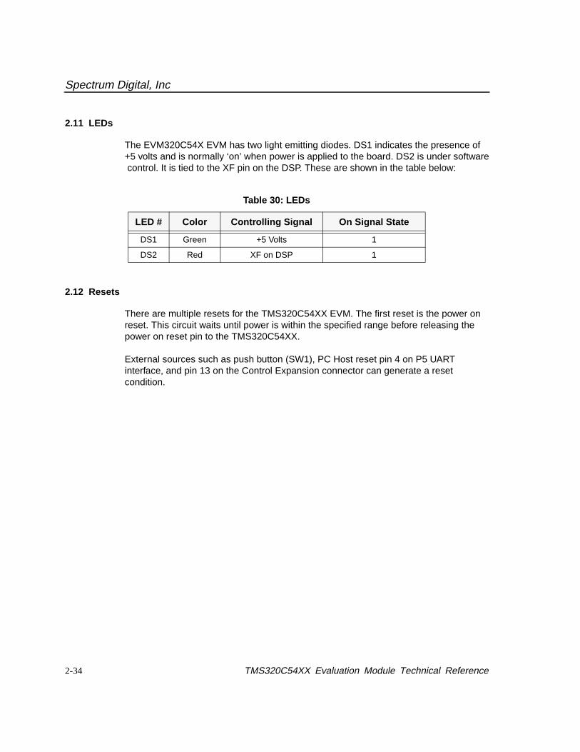
2.11 LEDs
The EVM320C54X EVM has two light emitting diodes. DS1 indicates the presence of+5 volts and is normally ‘on’ when power is applied to the board. DS2 is under software control. It is tied to the XF pin on the DSP. These are shown in the table below:
2.12 Resets
There are multiple resets for the TMS320C54XX EVM. The first reset is the power onreset. This circuit waits until power is within the specified range before releasing thepower on reset pin to the TMS320C54XX.
External sources such as push button (SW1), PC Host reset pin 4 on P5 UARTinterface, and pin 13 on the Control Expansion connector can generate a resetcondition.
Table 30: LEDs
LED # Color Controlling Signal On Signal State
DS1 Green +5 Volts 1
DS2 Red XF on DSP 1
A-1
Appendix A
TMS320C54XX EVM GAL Equations
This appendix lists the four GAL logic equations that are used on theTMS320C54XX Evaluation Module (EVM).
Topic Page
A.1.1 Memory Decode GAL Equations for VC5402 A-2A.1.2 Memory Decode GAL Equations for LC548, LC549, A-4
VC549, VC5410A.1.3 Memory Decode GAL Equations for VC5416 A-6A.2 I/O Control GAL Equations A-8

Spectrum Digital, Inc
A-2 TMS320C54XX Evaluation Module Technical Reference
A.1.1 Memory Decode GAL Equations for VC5420
The following GAL equations are used for the memory decode logic for VC5402
module _503123D flag ‘-r3’ title ‘Memory Decode Part Number: 503124-0001 Designer: Ron Peterson Rev C Feb 2,1998 Company: Spectrum Digital Inc. Copyright 1996 ‘
“ Device Declaration
U503123D device ‘P20V8C’;
“ Inputs
DS pin 2; “PS pin 3; “RW pin 4; “MSTRB pin 5; “IOSTRB pin 6 “A22 pin 7; “A21 pin 9; “A20 pin 10; “A19 pin 11; “A18 pin 12; “A17 pin 13; “IS pin 27; “A16 pin 16; “A15 pin 17; “UART pin 19; “IO3 pin 20; “
“ Outputs
INTERN pin 26; “RAM0WE pin 25; “RAM0OE pin 24; “RAM1WE pin 23; “RAM1OE pin 21; “ROM pin 18; “
Spectrum Digital, Inc
A-3
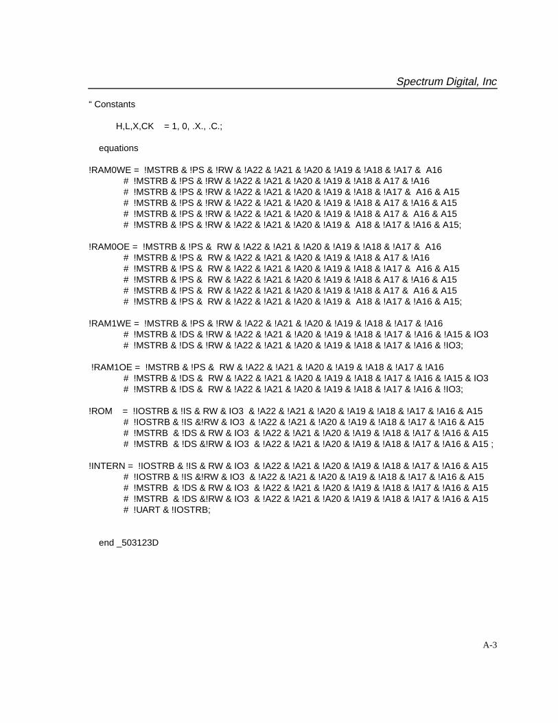
“ Constants
H,L,X,CK = 1, 0, .X., .C.;
equations
!RAM0WE = !MSTRB & !PS & !RW & !A22 & !A21 & !A20 & !A19 & !A18 & !A17 & A16 # !MSTRB & !PS & !RW & !A22 & !A21 & !A20 & !A19 & !A18 & A17 & !A16 # !MSTRB & !PS & !RW & !A22 & !A21 & !A20 & !A19 & !A18 & !A17 & A16 & A15 # !MSTRB & !PS & !RW & !A22 & !A21 & !A20 & !A19 & !A18 & A17 & !A16 & A15 # !MSTRB & !PS & !RW & !A22 & !A21 & !A20 & !A19 & !A18 & A17 & A16 & A15 # !MSTRB & !PS & !RW & !A22 & !A21 & !A20 & !A19 & A18 & !A17 & !A16 & A15;
!RAM0OE = !MSTRB & !PS & RW & !A22 & !A21 & !A20 & !A19 & !A18 & !A17 & A16 # !MSTRB & !PS & RW & !A22 & !A21 & !A20 & !A19 & !A18 & A17 & !A16 # !MSTRB & !PS & RW & !A22 & !A21 & !A20 & !A19 & !A18 & !A17 & A16 & A15 # !MSTRB & !PS & RW & !A22 & !A21 & !A20 & !A19 & !A18 & A17 & !A16 & A15 # !MSTRB & !PS & RW & !A22 & !A21 & !A20 & !A19 & !A18 & A17 & A16 & A15 # !MSTRB & !PS & RW & !A22 & !A21 & !A20 & !A19 & A18 & !A17 & !A16 & A15;
!RAM1WE = !MSTRB & !PS & !RW & !A22 & !A21 & !A20 & !A19 & !A18 & !A17 & !A16 # !MSTRB & !DS & !RW & !A22 & !A21 & !A20 & !A19 & !A18 & !A17 & !A16 & !A15 & IO3 # !MSTRB & !DS & !RW & !A22 & !A21 & !A20 & !A19 & !A18 & !A17 & !A16 & !IO3;
!RAM1OE = !MSTRB & !PS & RW & !A22 & !A21 & !A20 & !A19 & !A18 & !A17 & !A16 # !MSTRB & !DS & RW & !A22 & !A21 & !A20 & !A19 & !A18 & !A17 & !A16 & !A15 & IO3 # !MSTRB & !DS & RW & !A22 & !A21 & !A20 & !A19 & !A18 & !A17 & !A16 & !IO3;
!ROM = !IOSTRB & !IS & RW & IO3 & !A22 & !A21 & !A20 & !A19 & !A18 & !A17 & !A16 & A15 # !IOSTRB & !IS &!RW & IO3 & !A22 & !A21 & !A20 & !A19 & !A18 & !A17 & !A16 & A15 # !MSTRB & !DS & RW & IO3 & !A22 & !A21 & !A20 & !A19 & !A18 & !A17 & !A16 & A15 # !MSTRB & !DS &!RW & IO3 & !A22 & !A21 & !A20 & !A19 & !A18 & !A17 & !A16 & A15 ;
!INTERN = !IOSTRB & !IS & RW & IO3 & !A22 & !A21 & !A20 & !A19 & !A18 & !A17 & !A16 & A15 # !IOSTRB & !IS &!RW & IO3 & !A22 & !A21 & !A20 & !A19 & !A18 & !A17 & !A16 & A15 # !MSTRB & !DS & RW & IO3 & !A22 & !A21 & !A20 & !A19 & !A18 & !A17 & !A16 & A15 # !MSTRB & !DS &!RW & IO3 & !A22 & !A21 & !A20 & !A19 & !A18 & !A17 & !A16 & A15 # !UART & !IOSTRB;
end _503123D
Spectrum Digital, Inc
A-4 TMS320C54XX Evaluation Module Technical Reference
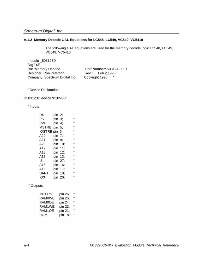
A.1.2 Memory Decode GAL Equations for LC548, LC549, VC549, VC5410
The following GAL equations are used for the memory decode logic LC548, LC549,VC549, VC5410
module _503123D flag ‘-r3’ title ‘Memory Decode Part Number: 503124-0001 Designer: Ron Peterson Rev C Feb 2,1998 Company: Spectrum Digital Inc. Copyright 1996 ‘
“ Device Declaration
U503123D device ‘P20V8C’;
“ Inputs
DS pin 2; “PS pin 3; “RW pin 4; “MSTRB pin 5; “IOSTRB pin 6 “A22 pin 7; “A21 pin 9; “A20 pin 10; “A19 pin 11; “A18 pin 12; “A17 pin 13; “IS pin 27; “A16 pin 16; “A15 pin 17; “UART pin 19; “IO3 pin 20; “
“ Outputs
INTERN pin 26; “RAM0WE pin 25; “RAM0OE pin 24; “RAM1WE pin 23; “RAM1OE pin 21; “ROM pin 18; “

Spectrum Digital, Inc
A-5
“ Constants
H,L,X,CK = 1, 0, .X., .C.;
equations
!RAM0WE = !MSTRB & !PS & !RW & !A19 & !A18 & !A17 & A16 # !MSTRB & !PS & !RW & !A19 & !A18 & A17 & !A16 # !MSTRB & !PS & !RW & !A19 & !A18 & !A17 & A16 & A15 # !MSTRB & !PS & !RW & !A19 & !A18 & A17 & !A16 & A15 # !MSTRB & !PS & !RW & !A19 & !A18 & A17 & A16 & A15 # !MSTRB & !PS & !RW & !A19 & A18 & !A17 & !A16 & A15;
!RAM0OE = !MSTRB & !PS & RW & !A19 & !A18 & !A17 & A16 # !MSTRB & !PS & RW & !A19 & !A18 & A17 & !A16 # !MSTRB & !PS & RW & !A19 & !A18 & !A17 & A16 & A15 # !MSTRB & !PS & RW & !A19 & !A18 & A17 & !A16 & A15 # !MSTRB & !PS & RW & !A19 & !A18 & A17 & A16 & A15 # !MSTRB & !PS & RW & !A19 & A18 & !A17 & !A16 & A15;
!RAM1WE = !MSTRB & !PS & !RW & !A19 & !A18 & !A17 & !A16 # !MSTRB & !DS & !RW & !A19 & !A18 & !A17 & !A16 & !A15 & IO3 # !MSTRB & !DS & !RW & !A19 & !A18 & !A17 & !A16 & !IO3;
!RAM1OE = !MSTRB & !PS & RW & !A19 & !A18 & !A17 & !A16 # !MSTRB & !DS & RW & !A19 & !A18 & !A17 & !A16 & !A15 & IO3 # !MSTRB & !DS & RW & !A19 & !A18 & !A17 & !A16 & !IO3;
!ROM = !IOSTRB & !IS & RW & IO3 & !A19 & !A18 & !A17 & !A16 & A15 # !IOSTRB & !IS &!RW & IO3 & !A19 & !A18 & !A17 & !A16 & A15 # !MSTRB & !DS & RW & IO3 & !A19 & !A18 & !A17 & !A16 & A15 # !MSTRB & !DS &!RW & IO3 & !A19 & !A18 & !A17 & !A16 & A15 ;
!INTERN = !IOSTRB & !IS & RW & IO3 & !A19 & !A18 & !A17 & !A16 & A15 # !IOSTRB & !IS &!RW & IO3 & !A19 & !A18 & !A17 & !A16 & A15 # !MSTRB & !DS & RW & IO3 & !A19 & !A18 & !A17 & !A16 & A15 # !MSTRB & !DS &!RW & IO3 & !A19 & !A18 & !A17 & !A16 & A15 # !UART & !IOSTRB;
end _503123D
Spectrum Digital, Inc
A-6 TMS320C54XX Evaluation Module Technical Reference
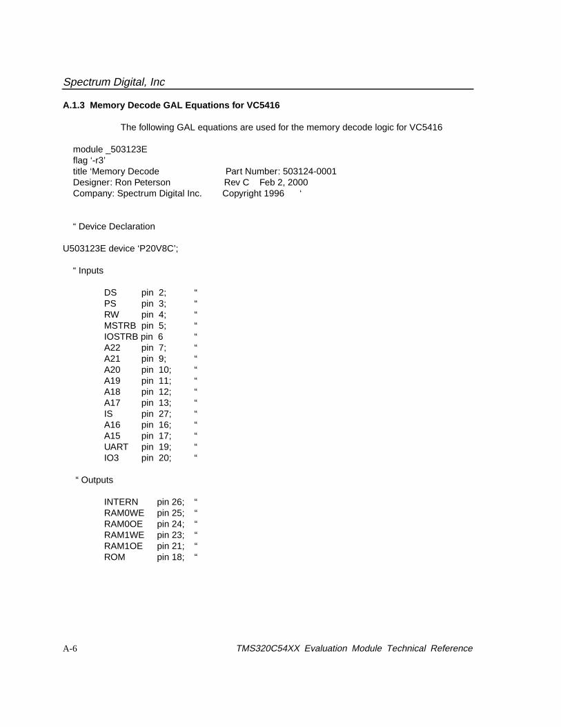
A.1.3 Memory Decode GAL Equations for VC5416
The following GAL equations are used for the memory decode logic for VC5416
module _503123E flag ‘-r3’ title ‘Memory Decode Part Number: 503124-0001 Designer: Ron Peterson Rev C Feb 2, 2000 Company: Spectrum Digital Inc. Copyright 1996 ‘
“ Device Declaration
U503123E device ‘P20V8C’;
“ Inputs
DS pin 2; “PS pin 3; “RW pin 4; “MSTRB pin 5; “IOSTRB pin 6 “A22 pin 7; “A21 pin 9; “A20 pin 10; “A19 pin 11; “A18 pin 12; “A17 pin 13; “IS pin 27; “A16 pin 16; “A15 pin 17; “UART pin 19; “IO3 pin 20; “
“ Outputs
INTERN pin 26; “RAM0WE pin 25; “RAM0OE pin 24; “RAM1WE pin 23; “RAM1OE pin 21; “ROM pin 18; “

Spectrum Digital, Inc
A-7
“ Constants
H,L,X,CK = 1, 0, .X., .C.;
equations
!RAM0WE = !MSTRB & !PS & !RW & !A22 & !A21 & !A20 & !A19 & & !A17 & A16 # !MSTRB & !PS & !RW & !A22 & !A21 & !A20 & !A19 & A17 & !A16 # !MSTRB & !PS & !RW & !A22 & !A21 & !A20 & !A19 & A16 & A15 # !MSTRB & !PS & !RW & !A22 & !A21 & !A20 & !A19 & !A16 & A15 # !MSTRB & !PS & !RW & !A22 & !A21 & !A20 & !A19 & A16 & A15 # !MSTRB & !PS & !RW & !A22 & !A21 & !A20 & !A19 & !A16 & A15;
!RAM0OE = !MSTRB & !PS & RW & !A22 & !A21 & !A20 & !A19 & !A18 & !A17 & A16 # !MSTRB & !PS & RW & !A22 & !A21 & !A20 & !A19 & A17 & !A16 # !MSTRB & !PS & RW & !A22 & !A21 & !A20 & !A19 & A16 & A15 # !MSTRB & !PS & RW & !A22 & !A21 & !A20 & !A19 & !A16 & A15 # !MSTRB & !PS & RW & !A22 & !A21 & !A20 & !A19 & A16 & A15 # !MSTRB & !PS & RW & !A22 & !A21 & !A20 & !A19 & !A16 & A15;
!RAM1WE = !MSTRB & !PS & !RW & !A22 & !A21 & !A20 & !A19 & !A18 & !A17 & !A16 # !MSTRB & !DS & !RW & !A22 & !A21 & !A20 & !A19 & !A18 & !A17 & !A16 & !A15 & IO3 # !MSTRB & !DS & !RW & !A22 & !A21 & !A20 & !A19 & !A18 & !A17 & !A16 & !IO3;
!RAM1OE = !MSTRB & !PS & RW & !A22 & !A21 & !A20 & !A19 & !A18 & !A17 & !A16 # !MSTRB & !DS & RW & !A22 & !A21 & !A20 & !A19 & !A18 & !A17 & !A16 & !A15 & IO3 # !MSTRB & !DS & RW & !A22 & !A21 & !A20 & !A19 & !A18 & !A17 & !A16 & !IO3;
!ROM = !IOSTRB & !IS & RW & IO3 & !A22 & !A21 & !A20 & !A19 & !A18 & !A17 & !A16 & A15 # !IOSTRB & !IS &!RW & IO3 & !A22 & !A21 & !A20 & !A19 & !A18 & !A17 & !A16 & A15 # !MSTRB & !DS & RW & IO3 & !A22 & !A21 & !A20 & !A19 & !A18 & !A17 & !A16 & A15 # !MSTRB & !DS &!RW & IO3 & !A22 & !A21 & !A20 & !A19 & !A18 & !A17 & !A16 & A15 ;
!INTERN = !IOSTRB & !IS & RW & IO3 & !A22 & !A21 & !A20 & !A19 & !A18 & !A17 & !A16 & A15 # !IOSTRB & !IS &!RW & IO3 & !A22 & !A21 & !A20 & !A19 & !A18 & !A17 & !A16 & A15 # !MSTRB & !DS & RW & IO3 & !A22 & !A21 & !A20 & !A19 & !A18 & !A17 & !A16 & A15 # !MSTRB & !DS &!RW & IO3 & !A22 & !A21 & !A20 & !A19 & !A18 & !A17 & !A16 & A15 # !UART & !IOSTRB;
end _503123E
Spectrum Digital, Inc
A-8 TMS320C54XX Evaluation Module Technical Reference
A.2 I/O Control GAL Equations
The following GAL equations are used for the I/O control logic
module _503124B flag ‘-r3’ title ‘UART & Target Control Part Number: 503124-0001 Designer: Ron Peterson Rev B Mar 2,1997 Company: Spectrum Digital Inc. Copyright 1996 ‘
“ Device Declaration
U503124B device ‘P16V8R’;
“ Inputs
CLK pin 1; “ Target ReadyIOSTRB pin 2; “ IO STROBERW pin 3; “ IO STROBEA15 pin 4; “ Address 15A14 pin 5; “ Address 14A13 pin 6; “ Address 13A12 pin 7; “ Address 12ROM pin 8; “ Rom SelectT_RDY pin 9; “ Target ReadyOE pin 11; “ Gnd
“ Outputs & Registered Outputs
WE pin 12; “ READUARTCS pin 13; “ ADSRD pin 14; “ WE-CNT0 pin 15; “ CNT0CNT1 pin 16; “ CNT1CNT2 pin 17; “ CNT2CNT3 pin 18; “ CNT3RDY pin 19; “ RDY
Spectrum Digital, Inc
A-9
“ Constant Declaration
H,L,X,CK = 1, 0, .X., .C.;Uart_States = [ CNT3,CNT2,CNT1,CNT0 ];
Address = [A15,A14,A13,A12,X,X,X,X,X,X,X,X,X,X,X,X];
UART_SEL = ((( Address >= ^h0000 ) & ( Address <= ^h0FFF ))& !IOSTRB);
“ State Assignments
“ CCCC“ NNNN“ TTTT“ 0123 Idle = ^b1111; Ads = ^b0111; Ads2 = ^b0011; Cyc1 = ^b0110; Cyc2 = ^b0010; Cyc3 = ^b0000; Cyc4 = ^b0001; Cyc5 = ^b0101; Cyc6 = ^b1101; Cyc7 = ^b1001; End_cyc = ^b1011;
state_diagram Uart_States
state Idle: if ((!IOSTRB ) # (!IOSTRB & !A15 & !A14 & !A13 & !A12) ) then Ads else Idle;
state Ads: goto Ads2;
state Ads2: goto Cyc1;
state Cyc1: goto Cyc2;state Cyc2: goto Cyc3;state Cyc3: goto Cyc4;state Cyc4: goto Cyc5;state Cyc5: goto Cyc6;state Cyc6: goto Cyc7;state Cyc7: goto End_cyc;
state End_cyc: if ( !IOSTRB) then End_cyc else Idle;
Spectrum Digital, Inc
A-10 TMS320C54XX Evaluation Module Technical Reference
equations
!RDY = (! T_RDY) # (( Uart_States == Ads) & !IOSTRB ) # (( Uart_States == Ads2) & !IOSTRB ) # (( Uart_States == Cyc1) & !IOSTRB ) # (( Uart_States == Cyc2) & !IOSTRB ) # (( Uart_States == Cyc3) & !IOSTRB ) # (( Uart_States == Cyc4) & !IOSTRB ) # (( Uart_States == Cyc5) & !IOSTRB ) # (( Uart_States == Cyc6) & !IOSTRB );
!UARTCS =( !A15 & !A14 & !A13 & !A12 & !IOSTRB );
!RD =(( Uart_States == Cyc1) & !IOSTRB & RW ) #(( !RD) & !IOSTRB & RW ) #( !ROM & RW );
!WE =(( Uart_States == Cyc1) & !IOSTRB & !RW ) #(( Uart_States != End_cyc) & !WE & !IOSTRB & !RW ) #( !ROM & !RW );
end _503124B

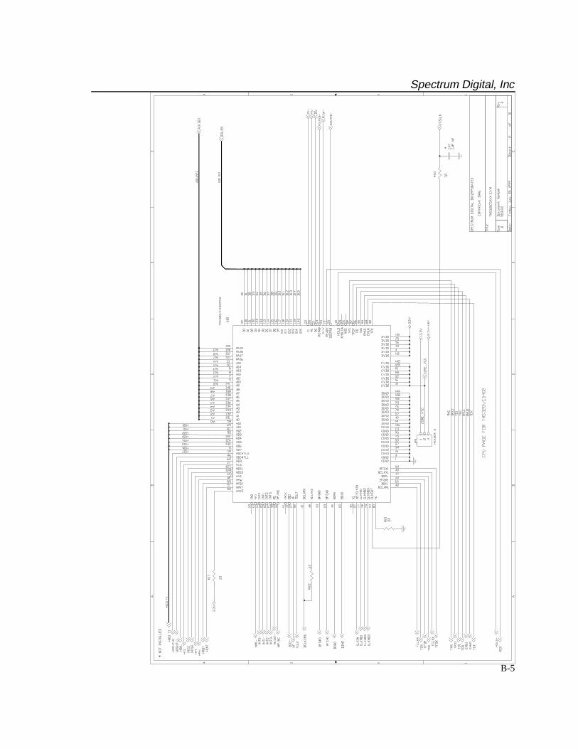
B-1
Appendix B
TMS320C54XX EVM Schematics
This appendix contains the schematics for the TMS320C54XX EVM. Theschematics were drawn on ORCAD.
Spectrum Digital, Inc
B-2 TMS320C54XX Evaluation Module Technical Reference

Spectrum Digital, Inc
B-3
Spectrum Digital, Inc
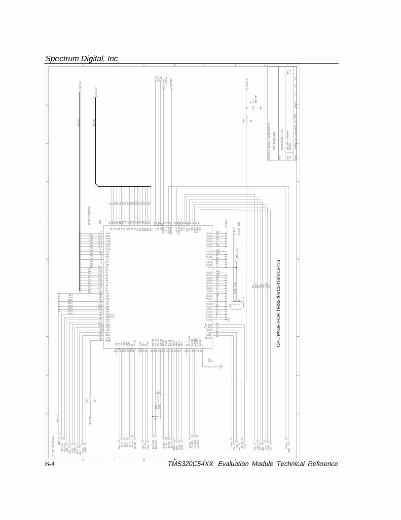
B-4 TMS320C54XX Evaluation Module Technical Reference
CP
U P
AG
E F
OR
TM
S32
0VC
5410
/VC
5416
Spectrum Digital, Inc
B-5

Spectrum Digital, Inc
B-6 TMS320C54XX Evaluation Module Technical Reference

Spectrum Digital, Inc
B-7

Spectrum Digital, Inc
B-8 TMS320C54XX Evaluation Module Technical Reference
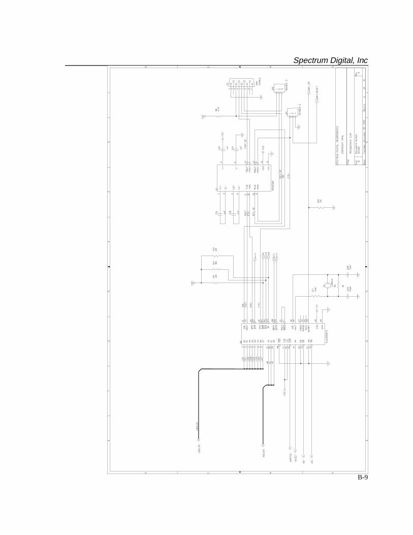
Spectrum Digital, Inc
B-9

Spectrum Digital, Inc
B-10 TMS320C54XX Evaluation Module Technical Reference

Spectrum Digital, Inc
B-11
D5,
D7,
D8
not i
nsta
lled
on V
c541
6
R47
=49
.9K
on V
C54
16R
46 n
ot in
stal
led
on V
C54
16

Spectrum Digital, Inc
B-12 TMS320C54XX Evaluation Module Technical Reference

Spectrum Digital, Inc
B-13

Spectrum Digital, Inc
B-14 TMS320C54XX Evaluation Module Technical Reference

C-1
Appendix C
TL16C550 Data Sheet
This appendix contains the programming data sheet for the TL16C550Asynchronous Communications Element (ACE) used on theTMS320C54XX Evaluation Module (EVM).
Topic Page
C.1 TL16C550 Serial Controller C-2C.1.1 Detailed Description C-2C.1.2 Line Control Register C-4C.1.3 Line Status Register C-6C.1.4 FIFO Control Register C-8C.1.5 Modem Control Register C-9C.1.6 Modem Status Register C-10C.1.7 Divisor Latches C-12C.1.8 Scratchpad Register C-13C.1.9 Interrupt Identification Register C-13C.1.10 Interrupt Enable Register C-15C.1.11 Receiver C-16C.1.12 Master Reset C-16C.1.13 Programming C-18C.1.14 FIFO Polled Mode Operation C-19

Spectrum Digital, Inc
C-2 TMS320C54XX Evaluation Module Technical Reference
C.1 TL16C550 SERIAL CONTROLLER
The EVM320C54XX uses a TL16C550 serial controller. The following sections describethe functionality of this device as it is used in the EVM320C54XX.
The TL16C550 UART resides at address 0x0010 in the I/O address space on theEVM320C54X.
C.1.1 DETAILED DESCRIPTION
Individual bits within the registers are referred to by the register mnemonic and the bitnumber in parenthesis. As an example, LCR (7) refers to line control register bit 7.
The transmitter buffer register and receiver buffer register are data registers that holdfrom five to eight bits of data. If less than eight data bits are transmitted, data is rightjustified to the LSB. Bit 0 of a data word is always the first serial data bit received andtransmitted. The ACE data registers are double buffered so that read and writeoperations may be performed when the ACE is performing the parallel-to-serial orserial-to-parallel conversion.
Spectrum Digital, Inc
C-3
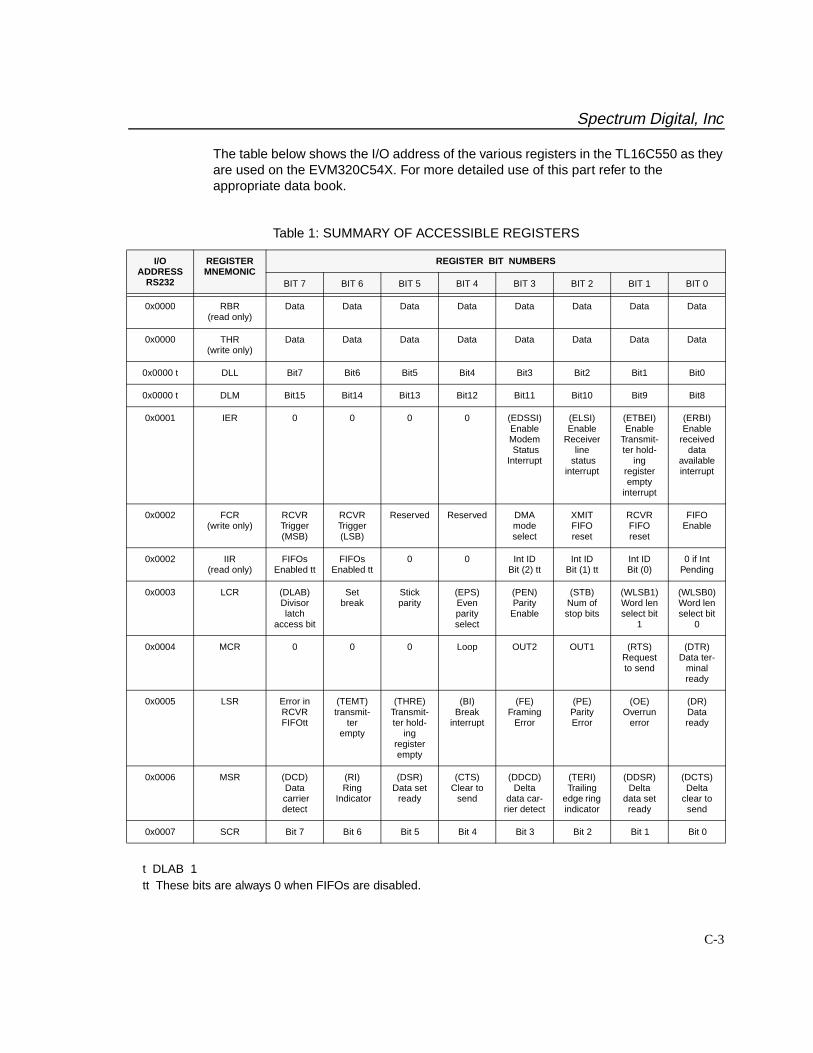
The table below shows the I/O address of the various registers in the TL16C550 as theyare used on the EVM320C54X. For more detailed use of this part refer to theappropriate data book.
t DLAB 1 tt These bits are always 0 when FIFOs are disabled.
Table 1: SUMMARY OF ACCESSIBLE REGISTERS
I/O ADDRESS
RS232
REGISTERMNEMONIC
REGISTER BIT NUMBERS
BIT 7 BIT 6 BIT 5 BIT 4 BIT 3 BIT 2 BIT 1 BIT 0
0x0000 RBR(read only)
Data Data Data Data Data Data Data Data
0x0000 THR(write only)
Data Data Data Data Data Data Data Data
0x0000 t DLL Bit7 Bit6 Bit5 Bit4 Bit3 Bit2 Bit1 Bit0
0x0000 t DLM Bit15 Bit14 Bit13 Bit12 Bit11 Bit10 Bit9 Bit8
0x0001 IER 0 0 0 0 (EDSSI)Enable Modem Status
Interrupt
(ELSI)Enable
Receiver line
status interrupt
(ETBEI)Enable
Transmit-ter hold-
ing register empty
interrupt
(ERBI) Enable
received data
available interrupt
0x0002 FCR(write only)
RCVRTrigger(MSB)
RCVRTrigger(LSB)
Reserved Reserved DMAmode select
XMITFIFOreset
RCVRFIFOreset
FIFOEnable
0x0002 IIR(read only)
FIFOsEnabled tt
FIFOsEnabled tt
0 0 Int IDBit (2) tt
Int IDBit (1) tt
Int IDBit (0)
0 if IntPending
0x0003 LCR (DLAB)Divisor latch
access bit
Setbreak
Stickparity
(EPS)Evenparityselect
(PEN)Parity
Enable
(STB)Num ofstop bits
(WLSB1)Word lenselect bit
1
(WLSB0)Word len select bit
0
0x0004 MCR 0 0 0 Loop OUT2 OUT1 (RTS)Request to send
(DTR)Data ter-
minal ready
0x0005 LSR Error in RCVR FIFOtt
(TEMT)transmit-
ter empty
(THRE)Transmit-ter hold-
ing register empty
(BI)Break
interrupt
(FE)Framing
Error
(PE)Parity Error
(OE)Overrun
error
(DR)Data ready
0x0006 MSR (DCD)Data
carrier detect
(RI)Ring
Indicator
(DSR)Data set
ready
(CTS)Clear to
send
(DDCD)Delta
data car-rier detect
(TERI)Trailing
edge ring indicator
(DDSR)Delta
data set ready
(DCTS)Delta
clear to send
0x0007 SCR Bit 7 Bit 6 Bit 5 Bit 4 Bit 3 Bit 2 Bit 1 Bit 0

Spectrum Digital, Inc
C-4 TMS320C54XX Evaluation Module Technical Reference
C.1.2 LINE CONTROL REGISTER (0x0003)
The format of the data character is controlled by the Line Control Register. The LCRmay be read. Its contents are described below and shown in Figure 1.
LCR(0) and LCR(1) Word Length Select Bits:
LCR(2) Stop Bits Select Bit 2:
LCR(2) specifies the number of stop bits in each transmitted character as shown belowand in table 21. The receiver always checks for one stop bit.
LCR(3) Parity Enable Bit 3:
When LCR(3) is high, a parity bit between the last data word bit and stop bit isgenerated and checked.
LCR(4) Even Parity Select Bit 4:
When enabled, a logic one selects even parity.
LCR(5) Stick Parity Bit 5:
When parity is enabled ( LCR(3) = 1, LCR(5) = 1 ) causes the transmission andreception of a parity bit to be in the opposite state from the value of LCR(4). This forcesparity to a known state and allows the receiver to check the parity bit in a known state.
Table 2: WORD LENGTH SELECT
LCR1 LCR0 Data bits
0 0 5 data bits
0 1 6 data bits
1 0 7 data bits
1 1 8 data bits
Table 3: STOP BIT SELECT
LCR2 Stop Bits
0 1 Stop Bit
1 1.5 Stop bits if 5 databits selected
1 2 Stop bits if 6,7,8data bits selected

Spectrum Digital, Inc
C-5
LCR(6) Break Control Bit 6:
When LCR(6) is set to a logic 1, the serial output (SOUT1/SOUT0) is for forced to thespacing state (low). The break control bit acts only on the serial output and does notaffect the transmitter logic. If the following sequence is used, no invalid characters willbe transmitted because of the break:
Step 1. Load a zero byte in response to the Transmitter Holding RegisterEmpty (THRE) status indication.
Step 2. Set the break in response to the next THRE status indication.
Step 3. Wait for the transmitter to be idle when transmitter empty status signalis set high (TEMT=1). Then clear the break when the normal transmissionhas to be restored.
LCR(7) Divisor Latch Access Bit (DLAB) bit 7:
Bit 7 must be set high (logic 1) to access the divisor latches DLL and DLM of the baudrate generator during a read or write operation. LCR(7) must be input low (logic 0) toaccess the receiver buffer register, the transmitter holding register or the interruptenable register.

Spectrum Digital, Inc
C-6 TMS320C54XX Evaluation Module Technical Reference
C.1.3 LINE STATUS REGISTER (0x0005)
The line status register (LSR) is a single register that provides status indications. Theline status register shown in table 21 and described below:
LSR(0) Data Ready (DR) Bit 0:
Data Ready is set high when an incoming character has been received and transferredinto the receiver buffer register or the FIFO. LSR(O) is reset low by a CPU read of thedata in the receiver buffer register or the FIFO.
LSR(1) Overrun Error (OE) bit 1:
Overrun Error indicates that data in the receiver buffer register was not read by theCPU before the next character was transferred into the receiver buffer registeroverwriting the previous character. The OE indicator is reset whenever the CPU readsthe contents of the line status register. An overrun error will occur in the FIFO modeafter the FIFO is full and the next character is completely received. The overrun error isdetected by the CPU on the first LSR read after it happens. The character in the shiftregister is not transferred to the FIFO but it is overwritten.
LSR(2) Parity Error (PE) bit 2:
Parity Error indicates that the received data character does not have the correct parityas selected by LCR(3) and LCR(4). The PE bit is set high upon detection of a parityerror and is reset low when the CPU reads the contents of the LSR. In the FIFO mode,the parity error is associated with a particular character in the FIFO, LSR(2) resets theerror when the character is at the top of the FIFO.
LSR(3) Framing Error (FE) bit 3:
Framing error indicates that the received character did not have a valid stop bit. LSR(3)is set high when the stop bit following the last data bit or parity bit is detected as a zerobit (spacing level). The FE indicator is reset low when the CPU reads the contents ofthe LSR. In the FIFO mode, the framing error is associated with a particular characterin the FIFO. LSR(3) reflects the error when the character is at the top of the FIFO.
Spectrum Digital, Inc
C-7
LSR(4) Break Interrupt (BI) bit 4:
Break Interrupt is set high when the received data input is held in the spacing (logic 0)state for longer than a full word transmission time (start bit + data bits + parity + stop bits). The BI indicator is reset when the CPU reads the contents of the line statusregister. In the FIFO mode, this is associated with a particular character in the FIFO.LSR(2) reflects the BI when the break character is at the top of the FIFO. The error isdetected by the CPU when its associated character is at the top of the FIFO during thefirst LSR read. Only one zero character is loaded into the FIFO when BI occurs.
LSR(4) - LSR(1) are the error conditions that produce a receiver line status interrupt (priority 1 interrupt in the Interrupt Identification register(IIR)) when any of theconditions are detected. This interrupt is enabled by setting IER(2) = 1 in the interruptenable register.
LSR(5) Transmitter Holding Register Empty (THRE) bit 5:
THRE Indicates that the ACE is ready to accept a new character for transmission. TheTHRE bit is set high when a character is transferred from the transmitter holdingregister into the transmitter shift register. LSR(5) is reset low by the loading of thetransmitter holding register by the CPU. LSR(5) is not reset by a CPU read of the LSR.In the FIFO mode when the XMIT FIFO is empty, this bit is set. It is cleared when onebyte is written to the XMIT FIFO. When the THRE Interrupt is enabled by IER(1), THREcauses a priority 3 interrupt in the IIR. If THRE is the interrupt source indicated In IIR,INTRPT is cleared by a read of the IIR.
LSR(6) Transmitter Empty (TEMT) bit 6:
TEMT is set high when the Transmitter Holding Register(THR) and the Transmitter ShiftRegister(TSR) are both empty. LSR(6) is reset low when a character is loaded into theTHR and remains low until the character is transferred out of SOUT. TEMT is not resetlow by a CPU read of the LSR. In FIFO mode, when both the transmitter FIFO and shift register are empty, this bit is set to one.
LSR(7) RCVR FIFO error bit 7:
The LSR(7) bit is always 0 in the TL16C450 mode. In FIFO mode, it is set when at leastone of the following data errors is in the FIFO: parity error, framing error, or breakinterrupt indication. It is cleared when the CPU reads the LSR if there are nosubsequent errors in the FIFO.
NOTE: The line status register may be written. However, this function is intended only forfactory test. It should be considered as read only by applications software.

Spectrum Digital, Inc
C-8 TMS320C54XX Evaluation Module Technical Reference
C.1.4 FIFO CONTROL REGISTER (0x0002)
This write only register is at the same location as the lIR. It is used to enable and clearthe FIFOs, set the trigger level of the RCVR FIFO, and select the type of DMAsignaling.
FCR(0) FIFO Enable
FIFO enables both the XMIT and RCVR FIFOS. All bytes in both FIFOs can be clearedby resetting FCR(0). Data is cleared automatically from the FIFOs when changing fromthe FIFO mode to the TL16C450 mode and vice versa. Programming of other FCR bitsis enabled by setting FCR(0) = 1.
FCR(1) Receiver FIFO Reset
FCR(1) = 1 clears all bytes In the RCVR FIFO and resets the counter logic to 0. Thisdoes not clear the shift register.
FCR(2) Transmit FIFO Reset
FCR(2) = 1 clears all bytes In the XMIT FIFO and resets the counter logic to 0. Thisdoes not clear the shift register.
FCR(3) DMA Mode Select
FCR(3) = 1 will change the RXRDY and TXRDY pins from mode 0 to mode 1 if FCR(0) = 1.
FCR(4) - FCR(5):
These two bits are reserved for future use.
FCR(6-7) FIFO Receiver Trigger
These two bits are used for setting the trigger level for the RCVR FIFO Interrupt afollows:
Table 4: FIFO Trigger Levels
Bit 7 Bit 6Receiver Fifo
Trigger Level (Bytes)
0 0 1
0 1 4
1 0 8
1 1 14
Spectrum Digital, Inc
C-9
C.1.5 MODEM CONTROL REGISTER (0x0004)
The Modem Control Register (MCR) controls the interface with the modem or data setas described in Figure 2. MCR can be written and read. The RTS and DTR outputs aredirectly controlled by their control bits in this register. A high input asserts a low(true) atthe output pins. MCR bits 0, 1, 2, 3, and 4 are shown as follows:
MCR(0) Data Terminal Ready
When MCR(0) is set high, the DTR output is forced low. When MCR(0) is reset low, theDTR output is forced high. The DTR output of the serial channel may be input into an inverting line driver in order to obtain the proper polarity input at the modem or data set.
MCR(1) Request to Send
When MCR(1) is set high, the RTS output is forced low. When MCR(1) is reset low, the RTS output is forced high. The RTS output of the serial channel may be input into an inverting line driver to obtain the proper polarity input at the modem or data set.
MCR(2) OUT1
When MCR(2) is set high, OUT1 is forced low.
MCR(3) OUT2
When MCR(3) is set high, the OUT2 output is forced low.
MCR(4) Loop
MCR(4) provides a local loopback feature for diagnostic testing of the channel. When MCR(4) is set high, serial output (SOUT) is set to the marking (logic 1) state, and the receiver data input serial input (SIN) is disconnected. The output of the transmitter shift register is looped back into the receiver shift register input. The four modem controlinputs (CTS, DSR, DCD, and RI) are disconnected. The modem control outputs (DTR,RTS, OUT1, and OUT2) are internally connected to the four modem control inputs. Themodem control outputs pins are forced to their inactive state(high) on the TL16C550. Inthe diagnostic mode, data transmitted is immediately received. This allows theprocessor to verify the transmission and receive data paths of the selected serialchannel. Interrupt control is fully operational. However, interrupts are generated bycontrolling the lower four MCR bits internally. Interrupts are not generated by activity onthe external pins represented by those four bits.
MCR(5) - MCR(7) are permanently set to logic 0.
Spectrum Digital, Inc
C-10 TMS320C54XX Evaluation Module Technical Reference
C.1.6 MODEM STATUS REGISTER (0x0006)
The MSR provides the CPU with status of the modem input lines from the modem orperipheral devices The MSR allows the CPU to read the serial channel modem signalinputs by accessing the data bus interface of the ACE in addition to the current status offour bits of the MSR that indicate whether the modem in inputs changed since the lastreading of the MSR. The delta status bits are set high when a control input from themodem changes state and reset low when the CPU reads the MSR.
The modem input lines CTS, DSR, RI and DCD. MSR(4) - MSR(7) are statusindications of these lines. A status bit = 1 indicates the input is a low. A status bit = 0indicates the input is high. If the modem status interrupt in the interrupt enable registeris enabled IER(3), an interrupt is generated whenever MSR(0) - MSR(3) is set to a one.The MSR is a priority 4 interrupt. The contents of the Modem Status Register aredescribed in Table 3.
MSR(0) Delta Clear to Send (DCTS) bit 0:
DCTS displays that the CTS input to the serial channel has changed state since it waslast read by the CPU.
MSR(1) Delta Data Set Ready (DDSR) bit 1:
DDSR indicates that the DSR input to the serial channel has changed state since thelast time it was read by the CPU.
MSR(2) Trailing Edge of Ring Indicator (TERI) bit 2:
TERI indicates that the RI input to the serial channel has changed state from low tohigh since the last time it was read by the CPU. High-to-low transitions on RI do notactivate TERI.
MSR(3) Delta Data Carrier Detect (DDCD) bit 3:
DDCD indicates that the DCD input to the serial channel has changed state since thelast time it was read by the CPU.
MSR(4) Clear to Send (CTS) bit 4:
CTS is the complement of the CTS input from the modem indicating to the serialchannel that the modem is ready to receive data from the serial channel’s transmitteroutput(SOUT). If the serial channel is in the loop mode MCR(4) = 1, MSR(4) reflectsthe value of RTS in the MCR.

Spectrum Digital, Inc
C-11
MSR(5) Data Set Ready (DSR) bit 5:
DSR is the complement of the DSR input from the modem to the serial channel that indicates that the modem is ready to provide received data to the serial channelreceiver circuitry, If the channel is in the loop mode MCR(4) = 1, MSR(5) reflects thevalue of DTR in the MCR.
MSR(6) Ring Indicator (RI) bit 6:
RI is the complement of the RI input. If the channel is in the loop mode MCR(4) = 1,MSR(6) reflects the value of OUT1 in the MCR.
MSR(7) Data Carrier Detect (DCD) bit 7:
Data carrier detect indicates the status of the data carrier detect DCD input. If thechannel is in the loop mode MCR(4) = 1, MSR(7) reflects the value of OUT2 in theMCR.
Reading the MSR register clears the delta modem status indications but has no effecton the other status bits. For LSR and MSR, the setting of status bits is inhibited duringstatus register read operations. If a status condition is generated during a readoperation, the status bit is not set until the trailing edge of the read. If a status bit is setduring a read operation, and the same status condition occurs, that status bit will becleared at the trailing edge of the read instead of being set again. In the loop backmode, when modem status interrupts are enabled, the CTS, DSR, RI and DCD inputpins are ignored. However a modem status interrupt may still be generated by writing toMCR3 - MCR0. Applications software should not write to the modem status register.
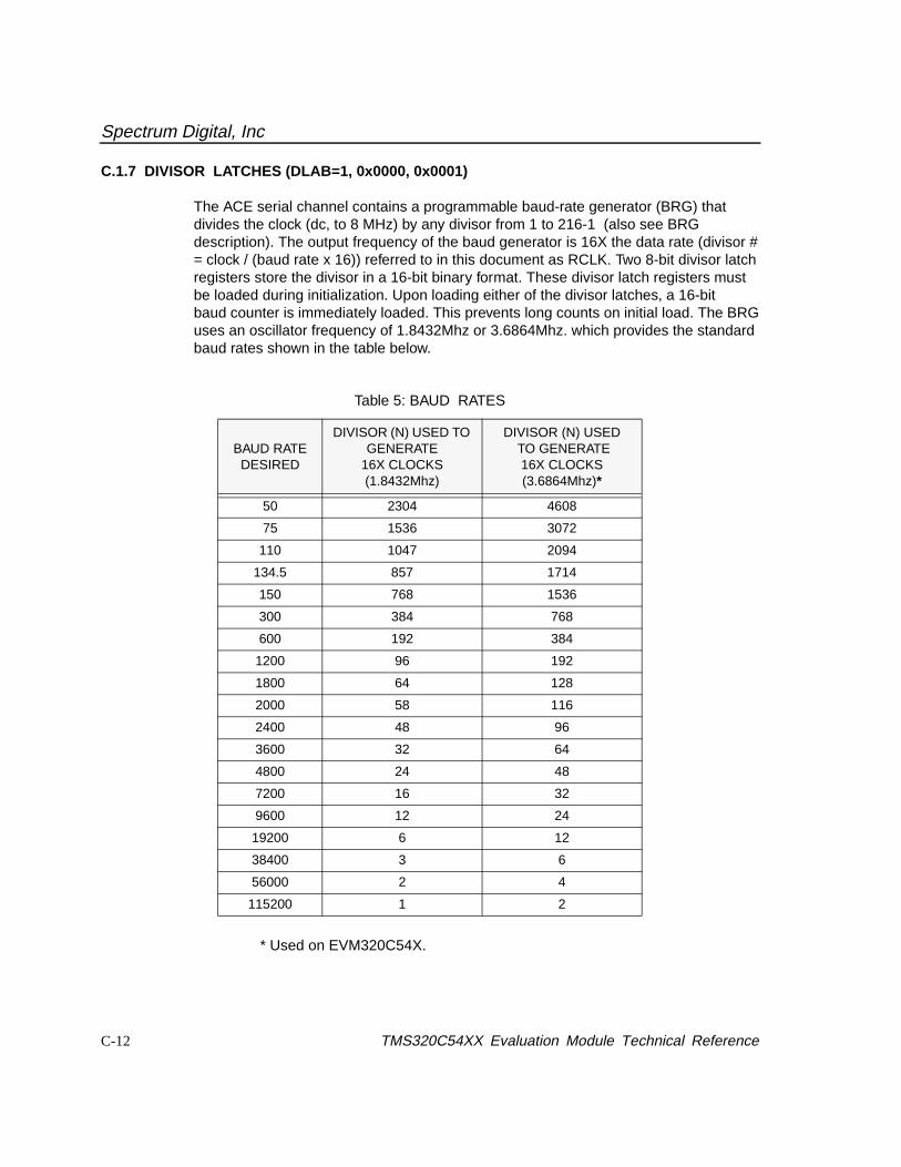
Spectrum Digital, Inc
C-12 TMS320C54XX Evaluation Module Technical Reference
C.1.7 DIVISOR LATCHES (DLAB=1, 0x0000, 0x0001)
The ACE serial channel contains a programmable baud-rate generator (BRG) thatdivides the clock (dc, to 8 MHz) by any divisor from 1 to 216-1 (also see BRGdescription). The output frequency of the baud generator is 16X the data rate (divisor #= clock / (baud rate x 16)) referred to in this document as RCLK. Two 8-bit divisor latchregisters store the divisor in a 16-bit binary format. These divisor latch registers mustbe loaded during initialization. Upon loading either of the divisor latches, a 16-bitbaud counter is immediately loaded. This prevents long counts on initial load. The BRGuses an oscillator frequency of 1.8432Mhz or 3.6864Mhz. which provides the standardbaud rates shown in the table below.
* Used on EVM320C54X.
Table 5: BAUD RATES
BAUD RATEDESIRED
DIVISOR (N) USED TO GENERATE
16X CLOCKS(1.8432Mhz)
DIVISOR (N) USED TO GENERATE
16X CLOCKS(3.6864Mhz)*
50 2304 4608
75 1536 3072
110 1047 2094
134.5 857 1714
150 768 1536
300 384 768
600 192 384
1200 96 192
1800 64 128
2000 58 116
2400 48 96
3600 32 64
4800 24 48
7200 16 32
9600 12 24
19200 6 12
38400 3 6
56000 2 4
115200 1 2

Spectrum Digital, Inc
C-13
C.1.8 SCRATCHPAD REGISTER (0x0007)
The scratchpad register is an 8-bit read/write register that has no effect on eitherchannel in the ACE. It is intended to be used by the programmer to hold datatemporarily.
C.1.9 INTERRUPT IDENTIFICATION REGISTER (0x0002)
In order to minimize software overhead during data character transfers, the serialchannel prioritizes interrupts into four levels. The four levels of Interrupt conditions areas follows:
1. Receiver line status (priority 1)
2. Received data ready (priority 2) or character time-out
3. Transmitter holding register empty (priority 3)
4. Modem status (priority 4)
Information indicating that a prioritized interrupt is pending and the type of interrupt isstored in the interrupt identification register (IIR). The IIR indicates the highest priorityinterrupt pending. The contents of the IIR are indicated in the table below.
Table 6: INTERRUPT IDENTIFICATION REGISTER
INTERRUPT IDENTIFICATIONREGISTER
INTERRUPT SET AND RESET
Bit 3 Bit 2 Bit 1 Bit 0PRIORITY
LEVELINTERRUPT
TYPEINTERRUPT
SOURCEINTERRUPT
RESET
0 0 0 1 None None None None
0 1 1 0 1 Receiver linestatus
OE, PE, FE,or BI
LSR read
0 1 0 0 2 Receiveddata available
Receiver dataavailable
RBR Read
1 1 0 0 2 Charactertime-out
indication
No charactershave beenreceived
RBR Read
0 0 1 0 3 THRE THRE IIR read orTHRE write
0 0 0 0 4 Modem status CTS, DSR, RI,or DCD
MSR read

Spectrum Digital, Inc
C-14 TMS320C54XX Evaluation Module Technical Reference
IIR(0) can be used to indicate whether an interrupt is pending. When IIR(0) is low, anInterrupt is pending.
IIR(1) and IIR(2) are used to identify the highest priority interrupt pending as indicatedin the table above.
IIR(3): This bit is always logic 0 when in the TL16C450 mode. This bit is set along withbit2 when in the FIFO mode and a trigger change level interrupt is pending.
IIR(4) - IIR(5): These two bits are always set to a logic 0.
IIR(6) - IIR(7): These two bits are always cleared in the TL16C450 mode. They are setwhen bit 0 of the FCR is set..

Spectrum Digital, Inc
C-15
C.1.10 INTERRUPT ENABLE REGISTER (0x0001)
The interrupt enable register (IER) is used to independently enable the four serialchannel interrupt sources that activate the interrupt (INT0 or INT1) output. All interruptsare disabled by resetting IER(0) - IER(3) of the interrupt enable register. Interrupts areenabled by setting the appropriate bits of the IER high. Disabling the interrupt systeminhibits the interrupt identification register and the active (high) interrupt output. Allother system functions operate in, their normal manner, including the setting of the linestatus and modem status registers. The contents of the interrupt enable register aredescribed below:
IER(0) Enable Received Data Available Interrupt
When set to one, IER(0) enables the received data available interrupt and the time-outinterrupts in the FIFO mode.
IER(1) Enable Transmitter Holding Register Empty Interrupt
When set to one, IER(1) enables the transmitter holding register empty interrupt.
IER(2) Enable Receiver Line Status Interrupt
When set to one IER(2) enables the receiver line status interrupt.
IER(3) Enable Modem Status Interrupt
When set to one, IER(3) enables the modem status Interrupt.
IER(4) - IER(7).
These four bits of the IER are logic 0.

Spectrum Digital, Inc
C-16 TMS320C54XX Evaluation Module Technical Reference
C.1.11 RECIEVER
Serial asynchronous data is input into the SIN pin. The ACE continually searches for ahigh-to-low transition from the idle state. When the transition is detected, a counter isreset, and counts the 16X clock to 7 1/2, which is the center of the start bit. The start bitis valid if the SIN is still low. Verifying the start bits prevents the receiver fromassembling a false data character due to a low-going noise spike on the SIN Input.
The Line Control Register determines the number of data bits in a character [LCR(0),LCR(1)]. If parity is used LCR(3) and the polarity of parity LCR(4) are needed. Statusfor the receiver is provided in the line status register. When a full character is received,including parity and stop bits, the data received indication in LSR(0) is set high. TheCPU reads the receiver buffer register, which resets LSR(0). If the character is not readprior to a new character transfer from the RSR to the RBR, the overrun error statusindication is set in LSR(1). If there is a parity error, the parity error is set in LSR(2). If astop bit is not detected, a framing error indication is set in LSR(3).
If the data into SIN is a symmetrical square wave, the center of the data cells will occurwith +/-3.125% of the actual center, providing an error margin of 46.875%. The start bitcan begin as much as one 1 6X clock cycle prior to being detected.
C.1.12 MASTER RESET
After power up, the ACE Reset Input should be held low for one microsecond to resetthe ACE circuits to an Idle mode until initialization. A low on RESET causes thefollowing:
1 . Initializes the transmitter and receiver clock counters.
2. Clears the Line Status Register (LSR), except for the transmitter shift register empty(TEMT) and transmit holding register empty (THRE), which are set. The Modem Control Register (MCR) is also cleared. All of the discrete lines, memory elements, and miscellaneous logic associated with these register bits are also cleared or turned off. The Line Control Register (LCR), divisor latches, receiver buffer register, and transmitter buffer register are not affected.
Following the removal of the reset condition (Reset high), the ACE remains in the idlemode until programmed.
A hardware reset of the ACE sets the THRE and TEMT status bit in the LSR. Wheninterrupts are subsequently enabled, an interrupt occurs due to THRE.
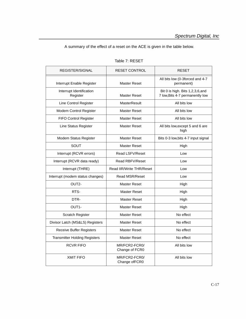
Spectrum Digital, Inc
C-17
A summary of the effect of a reset on the ACE is given in the table below.
Table 7: RESET
REGISTER/SIGNAL RESET CONTROL RESET
Interrupt Enable Register Master ResetAll bits low (0-3forced and 4-7
permanent)
Interrupt Identification Register Master Reset
Bit 0 is high. Bits 1,2,3,6,and7 low,Bits 4-7 permanently low
Line Control Register MasterResult All bits low
Modem Control Register Master Reset All bits low
FIFO Control Register Master Reset All bits low
Line Status Register Master Reset All bits low,except 5 and 6 arehigh
Modem Status Register Master Reset Bits 0-3 low,bits 4-7 input signal
SOUT Master Reset High
Interrupt (RCVR errors) Read LSFV/Reset Low
Interrupt (RCVR data ready) Read RBFV/Reset Low
Interrupt (THRE) Read IIR/Write THR/Reset Low
Interrupt (modem status changes) Read MSR/Reset Low
OUT2- Master Reset High
RTS- Master Reset High
DTR- Master Reset High
OUT1- Master Reset High
Scratch Register Master Reset No effect
Divisor Latch (MS&LS) Registers Master Reset No effect
Receive Buffer Registers Master Reset No effect
Transmitter Holding Registers Master Reset No effect
RCVR FIFO MR/FCR2-FCR0/Change of FCR0
All bits low
XMIT FIFO MR/FCR2-FCR0/Change ofFCR0
All bits low

Spectrum Digital, Inc
C-18 TMS320C54XX Evaluation Module Technical Reference
C.1.13 PROGRAMMING
The serial channel of the ACE is programmed by the control registers: LCR, IER, DLL,DLM, MCR, and FCR. These control words define the character length, number of stopbits, parity, baud rate, and modem interface.
While the control registers can be written in any order, the IER should be written lastbecause it controls the Interrupt enables. Once the serial channel is programmed andoperational, these registers can be updated any time the ACE serial channel is nottransmitting or receiving data.
FIFO Interrupt Mode Operation
The following RCVR status occurs when the RCVR FIFO and receiver Interrupts areenabled:
1. LSR(0) is set when a character is transferred from the shift register to the RCVR FIFO. When the FIFO is empty, It is reset.
2. IIR = 06 receiver line status interrupt has higher priority than the received data available Interrupt IIR = 04.
3. Receive data available interrupt will be issued to the CPU when the programmed trigger level is reached by the FIFO. As soon as the FIFO drops below its programmed trigger level, it will be cleared.
4. IIR = 04 (receive data available indication) also occurs when the FIFO reaches its trigger level. It is cleared when the FIFO drops below the programmed trigger level.
The following RCVR FIFO character time-out status occurs when RCVR FIFO andreceiver interrupts are enabled.
1. If the following conditions exist, a FIFO character time-out interrupt occurs.
– Minimum of one character in FIFO
– Last received serial character was longer than 4 continuous previous character times ago (If two stop bits are programmed, the second one is included in the time delay).
Spectrum Digital, Inc
C-19
– The last CPU read of the FIFO was more than 4 continuous character times earlier. At 300 baud and 12-bit characters, the FIFO time-out interrupt causes a latency of 160 ms maximum from received character to interrupt issued.
2. By using the RCLK input for a clock signal, the character times can be calculated. (The delay is proportional to the baud rate.)
3. The time-out timer is reset after the CPU reads the RCVR FIFO or after a new character is received, when there has been no time-out interrupt.
4. A time-out interrupt is cleared and the timer is reset when the CPU reads a character from the RCVR FIFO.
XMIT Interrupts occur as follows when the transmitter and XMIT FIFO interrupts areenabled (FCR0 = 1, IER = 1).
1. When the transmitter FIFO is empty, the transmitter holding register interrupt (IIR = 02)occurs. The interrupt is cleared as soon as the transmitter holding register is written to or the IIR is read. One to sixteen characters may be written to the transmit FIFO when servicing this interrupt.
2. The XMIT FIFO empty indications will be delayed one character time minus the last stop bit time whenever the following occurs:
THRE = 1 and there has not been a minimum of two bytes at the same time in XMITFIFO, since the last THRE = 1. The first transmitter interrupt after changing FCR0 willbe immediate, however, assuming it is enabled.
RCVR FIFO trigger level and character time-out interrupts have the same priority as the received data available interrupt. The transmitter holding register empty interrupt hasthe same priority as the transmitter FIFO empty interrupt.
C.1.14 FIFO POLLED MODE OPERATION
Resetting IER0, IER1, IER2, IER3, or all to zero, with FCR0 = 1, puts the ACE into theFIFO polled mode. RCVR and XMITER are controlled separately. Therefore, either orboth can be in the polled mode. In the FIFO polled mode there is no time-out conditionindicated or trigger level reached. However, the RCVR and XMIT FIFOs still have thecapability of holding characters. The LSR must be read to determine the ACE status.

Spectrum Digital, Inc
C-20 TMS320C54XX Evaluation Module Technical Reference

D-1
Appendix D
TLC320AD50C Data Sheet
This appendix provides you with a description of the TLC32AD50C SigmaDelta Interface Circuit.
Topic Page
D.1 Introduction D-3D.1.1 Features D-3D.1.2 Functional Block Diagram D-4D.1.3 Definitions and Terminology D-5D.1.4 Register Functional Summary D-6D.2 Functional Description D-7D.2.1 Device Functions D-7D.2.1.1 Operating Frequencies D-7D.2.1.2 ADC Signal Channel D-7D.2.1.3 DAC Signal Channel D-8D.2.1.4 Serial Interface D-8D.2.1.5 Register Programming D-8D.2.1.6 Sigma-Delta ADC D-8D.2.1.7 Decimation Filter D-9D.2.1.8 Sigma-Delta DAC D-9D.2.1.9 Interpolation Filter D-9D.2.1.10 Analog and Digital Loopback D-9D.2.1.11 FIR Overflow Flag D-9D.2.2 Terminal Functions D-10D.2.2.1 Reset and Power-Down Functions D-10D.2.2.1.1 Reset D-10D.2.2.1.2 Conditions of Reset D-10D.2.2.1.3 Software and Hardware Power Down D-10D.2.2.2 Master Clock Circuit D-11D.2.2.3 Data Out (DOUT) D-11D.2.2.3.1 Data Out, Master Mode D-11D.2.2.3.2 Data Out, Slave Mode D-11D.2.2.4 Data In (DIN) D-11

Spectrum Digital, Inc
D-2 TMS320C54XX Evaluation Module Technical Reference
Topic Page
D.2.2.5 FC (Hardware Program Terminal) D-12D.2.2.6 Frame-Sync Function D-12D.2.2.6.1 Frame Sync (FS ), Master mode D-12D.2.2.6.2 Frame Sync (FS ), Slave Mode D-12D.2.2.6.3 Frame-Sync Delayed (FSD ), Master Mode D-12D.2.2.6.4 Frame-Sync Delayed (FSD ), Slave Mode D-13D.2.2.7 Multiplexed Analog Input D-13D.2.2.8 Analog Input D-14D.3 Serial Communications D-15D.3.1 Primary Serial Communication D-15D.3.2 Secondary Serial Communication D-17D.3.3 Conversion Rate Versus Serial Port D-19D.3.4 Phone Mode Control D-19D.4 Register Set D-20D.4.1 Control 1 Register D-21D.4.2 Control 2 Register D-22D.4.3 Control 3 Register D-22D.4.4 Control 4 Register D-23

Spectrum Digital, Inc
D-3
D.1 Introduction
The TLC320AD50C provides high-resolution low-speed signal conversion fromdigital-to-analog(D/A) and from analog-to-digital (A/D) using oversampling sigma-deltatechnology. This device consists or two serial synchronous conversion paths (one foreach data direction) and includes an interpolation filter before the DAC and adecimation filter after the ADC (see Section D.1.2). Other overhead functions provideon-chip timing and control. The sigma-delta architecture produces high-resolutionanalog-to digital and digital-to-analog conversion at low system speeds and low cost.
The options and the circuit configurations or this device can be programmed throughthe serial interface. The options include reset, power down, communications protocol,serial clock rate, signal sampling rate, gain control, and test mode as outlined inSection D.5. The TLC320AD50C is characterized for operation from 0 C to 70 C.
D.1.1 Features
The TLC320AD50C has the following features:
• Single 5-V power supply voltage or 5-V analog and 3-V digital power supply voltages• Power dissipation (PD) of 100 mW maximum in the operating mode• Hardware power-down mode to 2,5 mW• General-purpose 16-bit signal processing• 1’s-complement data format• Typical 91-dB dynamic range• Minimum 88-dB total signal-to-(noise + distortion) for the ADC• Minimum 85-dB total signal-to-(noise + distortion) for the DAC• Differential architecture throughout the device• Internal reference voltage (Vref)• Internal 64 X oversampling for the adc and 256 X oversampling for the dac• Serial port interface• ALT DATA terminal provides data monitoring during secondary communication• System test mode, digital loopback test, and analog loopback test• Supports all V.34 sample rates• Supports business audio applications• Variable conversion rate selected as MCLK/(128 X N) or MCLK/(512 X N)• May be configured in master or slave mode• Supports up to three slave devices• Input and output gain control

Spectrum Digital, Inc
D-4 TMS320C54XX Evaluation Module Technical Reference
D.1.2 Functional Block Diagram
MONOUT
Decimation Filter
SINC
FilterFilter
FIRSigma-
ADC
BufferDelta
DigitalLoopback
Vref
Sigma-DeltaDAC
Buffer
Interpolation
Filter
I/OControl+N PLL +2 +4 +64
LowPassFilter
AnalogLoopback
MUX
MUX
MCLK
REFPREFM
INPINM
AUXPAUXM
OUTPOUTM
DOUT (2scomplement
DIN (2scomplementM/S
FSD
ALTDATA
FC
FS
SCLK
FLAG
Figure D-1, Block Diagram TLC320AD50C

Spectrum Digital, Inc
D-5
D.1.3 Definitions and Terminology
Data Transfer Interval The data transfer interval is the time during which data is transferred fromDOUT and to DIN. The interval is 16 shift clocks and the data transfer isinitiated by the falling edge or the frame-sync signal.
Signal Data Signal data refers to the input signal and all or the converted representationsthrough the ADC channel and returned through the DAC channel to theanalog output. This is contrasted with the purely digital software control data.
Primary Primary communications refers to the digital data transfer interval. Since theCommunications device is synchronous, The signal data words from the ADC channel and the
DAC channel occur simultaneously.
Secondary Secondary communications refers to the digital control and configurationCommunications data transfer interval into DIN and the register read data cycle from DOUT.
The data transfer interval occurs when requested by hardware or software
Frame Sync Frame sync refers only to the falling edge or the signal that initiates the datatransfer interval. The primary frame sync starts the primary communications,and the secondary frame sync starts the secondary communications.
Frame Sync and Frame sync and sampling period is the time between falling edges orSampling Period successive primary frame-sync signals.
fs The sampling frequency that is the reciprocal of the sampling period.
Frame-Sync Interval Frame-sync interval is the time period occupied by 256 shift clocks. Theframe-sync signal goes high on the sixteenth rising edge or SCLK after thefalling edge or the frame-sync signal.
ADC Channel ADC Channel refers to all signal processing circuits between the analog inputand the digital conversion results at DOUT.
DAC Channel DAC channel refers to all signal processing circuits between the digital dataword applied to DIN and the differential output analog signal available atOUTP and OUTM.
Host A host is any processing system that interfaces to DIN, DOUT, SCLK, or FS.
Dxx Dxx is the bit position in the primary data word (xx is the bit number).
DSxx DSxx is the bit position the secondary data word (xx is the bit number).

Spectrum Digital, Inc
D-6 TMS320C54XX Evaluation Module Technical Reference
d The alpha character d represents valid programmed or default data in thecontrol register format (see Section D.3.2, Secondary Serial Communication)when discussing other data bit portions or the register.
X The alpha character X represents a don’t care bit position within the controlregister format.
FIR Finite duration inpulse response
D.1.4 Register Functional Summary
There are seven data and control registers that are used as follows:
Register 0 The No-Op register. The 0 address allows secondary requests withoutaltering any other register.
Register 1 The control 1 register. The data in this register controls:• The software reset• The software power down• Normal or auxiliary analog inputs enabling• Selection or the digital loopback• 16-bit or 15-bit mode of operation• Selection of monitor amplifier output gain• Selection of hardware or software secondary request mode
Register 2 The Control 2 register. The data in this register:• Contains the output flag indicating a decimator FIR filter overflow• Contains the output value or FLAG• Enables the ALTDATA input• Selects either 16-bit mode or 15-bit mode for the ADC• Enables analog loopback
Register 3 The control 3 register. The data in this register:• Selects the number or SCLK delays between FS and FSD• Informs the master device of how many slaves are connected in the chain.
Register 4 The Control 4 register. The data in this register:• Select the amplifier gain for the input and output amplifiers• Sets the sample rate by choosing the value or N from 1 to 8 where fs=MCLK/(128 X N) or MCLK/(512 X N)• Enables the external sample clock input at the MCLK input and bypasses the internal PLL. When enabled, the sample rate is set to MCLK/(512 X N) (see Subsection D.2.1.1, Operating Frequencies for more details.)
Register 14 Reserved for factory test. Do not write to this register.
Register 15 Reserved for factory test. Do not write to this register.

Spectrum Digital, Inc
D-7
D.2 Functional Description
D.2.1 Device Functions
D.2.1.1 Operating Frequencies
The sampling (conversion) frequency is derived from the master clock (MCLK) input byequation 1.
fs = Sampling (conversion) frequency = MCLK/128xN (when bit D7 or register 4 is setto 0) (1) where N is set by the contents or register 4 (bits D4 - D6) is 000, it defaults toN = 8. Otherwise, N is set by the octal representation of register 4 (bits D4 - D6). Thisis valid for sample rated higher than 7 kHz.
For sample rates lower than 7 kHz, the external sample clock feature must be enabled. This is done by setting bit D7 of Control 4 register equal to 1. This then bypasses theinternal clock phase lock loop (PLL) and sets the sampling frequency according toequation 2.
fs = MCLK/512 x N (when bit D7 or register 4 is set to 1)
This feature can be enabled for any sample rate, but must be enabled for sample rateslower than 7 kHz. The default value for register 4 bit D7 is 1. In all cases where theexternal sample clock is not used, 200us must be allowed following a change in thevalue or N for the PLL to settle. During this period, there is no signal output on theframe-sync or shift clock terminals. The inverse or the sample frequency is the timebetween the falling edges or two successive primary frame-sync signals which is theconversion period.
D.2.1.2 ADC Signal Channel
To produce excellent common-mode rejection of unwanted signals, the analog signal isprocessed differentially until it is converted to digital data.
The input signal is filtered and applied to the ADC input. The ADC converts the signalinto discrete output digital words in 2’s-complement data format, corresponding to theanalog-signal value at the sampling time. These 16-bit digital words, representingsampled values or the analog input signal, are clocked out or the serial port (DOUT)during the frame-sync interval, one word for each primary communication interval. During secondary communications, the data previously programmed into the registerscan be read out with the appropriate register address, and the read bit set to 1. If aregister read is not requested, all 16 bits are cleared to 0 in the secondary word.

Spectrum Digital, Inc
D-8 TMS320C54XX Evaluation Module Technical Reference
D.2.1.3 DAC Signal Channel
DIN receives the the 16-bit serial data word (2’s complement) from the host during theprimary communications interval and latches the data on the seventeenth rising edgeor SCLK. The data are converted to a pulse train by the sigma-delta DAC comprised ora digital interpolation filter and a digital 1-bit modulator. The output or the modulator isthen passed to an internal low-pass filter to complete the signal reconstruction resultingin an analog signal.
D.2.1.4 Serial Interface
The digital serial interface consists or the shift clock, the frame-sync signal, theADC-channel data output, and the DAC-channel data input. During the primary 16-bitframe synchronization interval, SCLK transfers the ADC channel results from DOUTand transfers 16-bit DAC data into DIN.
During the secondary frame-sync interval, SCLK transfers the register read data fromDOUT if the read bit is set to 1. In addition, SCLK transfers control and deviceparameter information into DIN. The timing sequence is shown in Figure 3-1.
D.2.1.5 Register Programming
All register programming occurs during secondary communications, and data arelatched and valid on the rising edge or the frame-sync signal. If the default value for aparticular register is desired, that register does not need to be addressed during thesecondary communications. The no-op command addressed the pseudo-register(register 0), and no register programming takes place during communications.
DOUT is released from he high-impedance state on the falling edge or the primary orsecondary frame-sync interval. In addition, each register can be read back duringDOUT secondary communications by setting the read bit D13 to 1. When the registeris in the read mode, no data can be written to the register during this cycle. To returnthis register to the write mode requires a subsequent secondary communication.
D.2.1.6 Sigma-Delta ADC
The sigma-delta ADC is a fourth-order sigma-delta modulator with 64x oversampling. The ADC provides high-resolution, low-noise performance using oversamplingtechniques.

Spectrum Digital, Inc
D-9
D.2.1.7 Decimation Filter
The decimation filter reduces the digital data rate to the sampling rate. This isaccomplished by decimating with a ratio of 1:64. The output or the decimation filter isa 16-bit 2’s-complement data word clocking at the sample rate selected.
NOTE:The sample rate is determined through a relationship or MCLK/(128 x N) where N is setby bits D4 - D6 of register 4 when bit D7 or register 4 is cleared to 0. The relationshipwhen bit D7 of register 4 is set to 1 is MCLK/(512 x N)
D.2.1.8 Sigma-Delta DAC
The sigma-delta DAC is a second-order sigma-delta modulator with 256 timesoversampling. The DAC provides high-resolution, low-noise performance from a 1-bitconverter using oversampling techniques. The TLC320AD50C provides a voltageoutput DAC.
D.2.1.9 Interpolation Filter
The interpolation filter resamples the digital data at a rate of 256x the incoming samplerate. The high-speed data output from the interpolation filter is then used in thesigma-delta DAC.
D.2.1.10 Analog and Digital Loopback
The loopbacks provide a means or testing the ADC and DAC channels and can beused for in-circuit system-level tests. The loopbacks feed the appropriate output to thecorresponding input on the IC.
The test capabilities include an analog loopback between the two analog paths and adigital loopback between the two digital paths. Digital loopback is enabled by setting bitD1 in Control 1 register: Analog loopback is enabled by setting bit D3 in Control 2register (see Section D.5, Register Set).
D.2.1.11 FIR Overflow Flag
The decimator FIR filter provides an overflow flag to Control 2 register to indicate thatthe input to the filter has exceeded the range or the internal filter calculations. Whenthe FIR overflow flag (Control 2 register bit D5) is set in the register, it remains set untilthe register is read by the user. Reading this value always resets the overflow flag.

Spectrum Digital, Inc
D-10 TMS320C54XX Evaluation Module Technical Reference
D.2.2 Terminal Functions
D.2.2.1 Reset and Power-Down Functions
D.2.2.1.1 Reset
The TLC320AD50C resets both the internal counters and registers, including theprogrammed registers, in two ways:
1. By applying a low-going reset pulse to the reset terminal2. By writing to the programmable software reset bit (D7 in Control 1 register)
PWRDWN resets the counters only and preserves the programmed register contents. The PWRDWN terminal must be kept low 20ms after the power supplies have settled.
D.2.2.1.2 Conditions of Reset
The two internal reset signals used for the reset and synchronization functions are:
1. Counter reset - The counter reset signal resets all flip-flops and latches that are not externally programmed, with the exception or those generating the reset pulse itself. Additionally, this signal resets the software power-down bit. A counter reset es initiated with the RESET terminal or RESET bit or PWRDWN terminal.
2. Register reset - The register reset signal resets all flip-flops and latches that are not reset by the counter reset, except those generating the reset pulse itself. A register reset is initiated with the RESET terminal or RESET bit.
Both reset signals must be at least six master clock periods long, TRESET, and releaseson the trailing edge or the master clock.
D.2.2.1.3 Software and Hardware Power Down
Given the definitions above, the software-programmed power-down condition is clearedby programming the software bit (Control 1 register, bit 6) to 0 or by cycling the power tothe device or bringing RESET low.
The output of the monitor amplifier maintains its midpoint voltage during hardware andsoftware power down to minimize pops and clicks.
If PWRDWN is not used, it should be tied high. The power drawn during a softwarepower down is higher than during a hardware power down. This is due to the currentdrawn to keep the digital interface running.

Spectrum Digital, Inc
D-11
D.2.2.2 Master Clock Circuit
The clock circuit generates and distributes necessary clocks throughout the device. MCLK is the external master clock input. An internal PLL circuit is used for upsamplingto provide the appropriate clocks for the digital filters and modulators. When in mastermode, SCLK is derived from MCLK in order to provide clocking of the serialcommunications between the device and a digital signal processor. When in slavemode, SCLK and MCLK are both inputs. The sample rate of the data paths is set asMCLK/(128 x N) where N is set by the contents or bits D4 - D6 of Control 4 registerwhen bit D7 or Control 4 register is cleared to 0. This is only valid for sample ratesgreater than 7 kHz.
For sample rates lower than 7 kHz, the internal PLL must be bypassed by enabling theexternal sample clock feature (setting bit D7 or Control 4 register to 1. This changesthe relationship between the master clock frequency and the sample rate. When thisfeature is enabled, the sample rate of the data paths is set as MCLK/(512 x N). Thisfeature can be enabled for sample rates higher than 7 kHz.
D.2.2.3 Data Out (DOUT)
DOUT is placed in the high-impedance state on the sixteenth rising edge of SCLK(internal or external) after the falling edge or the frame sync. In the primarycommunication, the data word is the ADC conversion result. In the secondarycommunication, The data is the register read results when requested by the read/write(R/W) bit with the eight MSBs set 0 (see Section D.3, Serial Communication). If aregister read is not requested, the secondary word is all zeros. The state or themaster/slave terminal is reflected by the MSB in secondary communication and theLSB in the primary communication. When the device is in the slave mode, DOUTremains as 3-state during initialization until a nonzero value is written to Control 3register (bits D7 and D6).
D.2.2.3.1 Data Out, Master Mode
In the master mode, DOUT is taken from the high-impedance state by the falling edgeor the frame sync. The most significant data bit then appears on DOUT.
D.2.2.3.2 Data Out, Slave Mode
In the slave mode, DOUT is taken from the high-impedance state by the falling edge ofthe external frame sync. The most significant data bit then appears on DOUT. When inslave mode, DOUT is not enabled until Control 3 register is programmed with thenumber of slaves. This must be done even if there is only one slave device.
D.2.2.4 Data In (DIN)
In a primary communication, the data word is the input digital signal to the DACchannel. In a secondary communication, the data is the control and configuration datasets the device for a particular function (see Section 3.2, Serial Communications). TheLSB or Control 1 register determines whether the input is 15 bits or 16 bits.
Spectrum Digital, Inc
D-12 TMS320C54XX Evaluation Module Technical Reference
D.2.2.5 FC (Hardware Program Terminal)
The FC input provides for hardware programming requests for secondarycommunication. FC works in conjunction with the control bit D0 or the secondary dataword. The signal on FC is latched on the rising edge of the primary frame sync. SeeFigure B5-4 for the FC timing diagrams. FC should be tied low if not used (see SectionD.3.2. Secondary Serial Communications).
D.2.2.6 Frame-Sync Function
The frame-sync signal indicates the device is ready to send and receive data. The datatransfer from DOUT and into DIN begins on the falling edge of the frame-sync signal.
D.2.2.6.1 Frame Sync (FS ), Master Mode
The frame sync is generated internally and goes low on the rising edge of SCLK andremains low during a 16-bit data transfer. In addition to generating its own frame-syncsignal, the master also outputs a frame sync for each slave that is being used.
D.2.2.6.2 Frame Sync (FS ), Slave Mode
The frame-sync timing is generated externally by the master, is applied to FS or theslave, and controls the ADC and DAC timing in the case or a single slave. The externalframe-sync width must be a minimum or one shift clock to be recognized and can be aslong as 16 shift clocks.
D.2.2.6.3 Frame-Sync Delayed (FSD ), Master Mode
For the master, the frame-sync delayed output occurs 1/2 shift-clock period ahead orFS to compensate for the time delay through the master and slave devices. The timingrelationships are as Follows:
1. When the FSD register data is 0, then FSD goes low 1/4 SCLK prior to the rising edge of SCLK when FS goes low (see Figure 5-1).
2. When the FSD register data is greater than 17, FSD goes low on the rising edge or SCLK that is the FSD register number or SCLKs after the falling edge or FS.
Register data values from 1 to 17 result in a default register value or zero and shouldnot be used.
In either master or slave mode, if the number or slave devices (bits D0 and D1 orControl 2 register) is set to 0, then FSD is disabled.

Spectrum Digital, Inc
D-13
D.2.2.6.4 Frame-Sync Delayed (FSD ), Slave Mode
The master FSD is output to the first slave and the first slave FSD is output to thesecond slave device and so on. The FSD output or each device is input to the FSterminal or the succeeding device. The FSD timing sequence in the slave mode is asfollows:
1. When the FSD register data is 0, then FSD toes low after FS goes low (see Figure D4-2).
2. When the FSD register data is greater than 17, FSD goes low on the rising edge or SCLK that is the FSD register number or SCLKs after the falling edge or FS.
Data values from 1 to 17 should not be used.
D.2.2.7 Multiplexed Analog Input
The two differential analog inputs (INP and INM or AUXP and AUXM) are multiplexedinto the sigma-delta modulator. The performance or the AUX channel is similar to thenormal input channel. A simple rc antialias filter must be connected to AUXP andAUXM (also INP and INM if used). Amplifiers are provided to set the gain or eachinput. The gain of these amplifiers is set by the contents or control 4 register (seeSection D.5, Register Set for details).
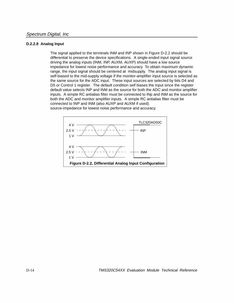
Spectrum Digital, Inc
D-14 TMS320C54XX Evaluation Module Technical Reference
D.2.2.8 Analog Input
The signal applied to the terminals INM and INP shown in Figure D-2.2 should bedifferential to preserve the device specifications. A single-ended input signal sourcedriving the analog inputs (INM, INP, AUXM, AUXP) should have a low sourceimpedance for lowest noise performance and accuracy To obtain maximum dynamicrange, the input signal should be centered at midsupply. The analog input signal isself-biased to the mid-supply voltage if the monitor-amplifier input source is selected asthe same source for the ADC input. These input sources are selected by bits D4 andD5 or Control 1 register. The default condition self biases the input since the registerdefault value selects INP and INM as the source for both the ADC and monitor amplifierinputs. A simple RC antialias filter must be connected to INp and INM as the source forboth the ADC and monitor amplifier inputs. A simple RC antialias filter must beconnected to INP and INM (also AUXP and AUXM if used).source-impedance for lowest noise performance and accuracy.
4 V
1 V
2.5 V
4 V
1 V
2.5 V
INP
INM
TLC320AD50C
Figure D-2.2, Differential Analog Input Configuration

Spectrum Digital, Inc
D-15
D.3 Serial Communications
DOUT, DIN, SCLK, FS, and FC are the serial communication signals. The digitaloutput data from the ADC is taken from DOUT. The digital input data for the DAC isapplied to DIN. The synchronizing clock for the serial communication data and theframe sync is taken from SCLK. The frame-sync pulse that enclosed the ADC and DACdata transfer interval is taken from FS. For signal (audio) data transmitted from theADC or to the DAC, primary serial communication is used. To read or write words thatcontrol both the options and the circuit configurations of the device, secondarycommunication is use.
The purpose of the primary and secondary communications is to allow conversion dataand control data to be transferred across the same serial port. A primary transfer isalways dedicated to conversion data. A secondary transfer is used to set up and readthe register values described in Section D.5, Register Set. A primary transfer occurs forevery conversion period. A secondary transfer occurs only when requested. Twomethods exist for requesting a secondary command. The FC terminal can request asecondary communication when it es asserted, or the LSB or the DAC data within aprimary transfer can request a secondary communication. The selection or whichmethod is enabled is provided in Control 1 register (bit D0) as shown in Section D.5,Register Set.
For all serial communications, the most significant bit is transferred first. For a 16-bitADC word and a 16-bit DAC word, D15 is the most significant bit and D0 is the leastsignificant bit. For a 15-bit DAC data word in a 16-bit primary communication, D15 isthe most significant bit, D1 is the least significant bit, and D0 is used for the embeddedfunction control. All digital data values are in 2’s-complement data format.
These logic signals are compatible with TTL-voltage levels and CMOS current levels (when VDD=5 Vdc). These logic signals are also compatible with a 3-V supply.
D.3.1 Primary Serial Communication
Primary serial communication is used both to transmit and receive conversion signaldata. The ADC word length can be either 15 bits or 16 bits. In master mode with FSDdisabled, it is always 16 bits. In slave mode, it is always 15 bits. The DAC word lengthdepends on the status or D0 in Control 1 register. After power up or reset, the devicedefaults to 15-bit mode (not 16-bit mode). The DAC word length is 15 bits and the lastbit of the primary 16-bit serial communication word is a function control bit used torequest secondary serial communication. In 16-bit mode, all 16 bits of the primarycommunication word are used as data for the DAC and the hardware terminal FC mustbe used to request secondary communication.
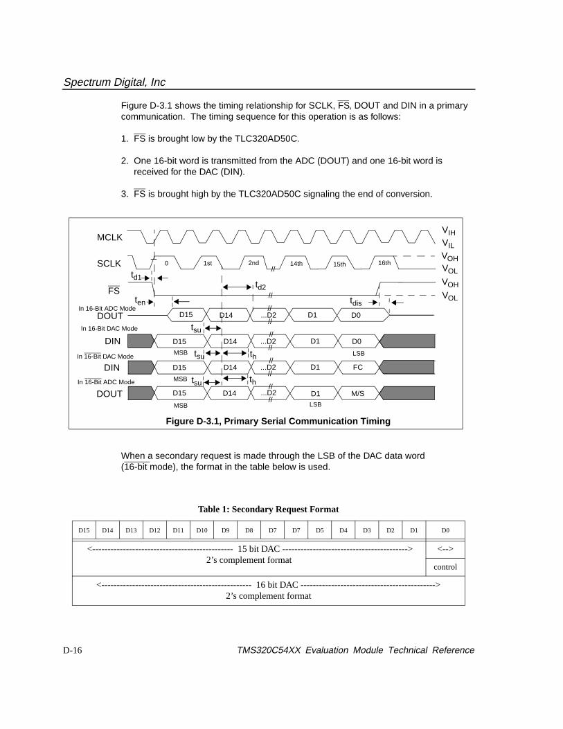
Spectrum Digital, Inc
D-16 TMS320C54XX Evaluation Module Technical Reference
Figure D-3.1 shows the timing relationship for SCLK, FS, DOUT and DIN in a primarycommunication. The timing sequence for this operation is as follows:
1. FS is brought low by the TLC320AD50C.
2. One 16-bit word is transmitted from the ADC (DOUT) and one 16-bit word is received for the DAC (DIN).
3. FS is brought high by the TLC320AD50C signaling the end of conversion.
When a secondary request is made through the LSB of the DAC data word(16-bit mode), the format in the table below is used.
Table 1: Secondary Request Format
D15 D14 D13 D12 D11 D10 D9 D8 D7 D7 D5 D4 D3 D2 D1 D0
<---------------------------------------------- 15 bit DAC ----------------------------------------->2’s complement format
<-->
control
<------------------------------------------------- 16 bit DAC -------------------------------------------->2’s complement format
MCLK
SCLK
FS
DOUT
DIN
DIN
DOUT
In 16-Bit ADC Mode
In 16-Bit DAC Mode
In 16-Bit DAC Mode
In 16-Bit ADC Mode
VIH
//
VIL
VOHVOL
VOH
VOL
D15 D14 ...D2 D1 M/S
FCD1D15
D14 ...D2D15
D14 ...D2
D15 D14 ...D2
D1 D0
D1 D0
LSB
LSBMSB
MSB
MSB
0 1st 2nd 14th 15th 16th
Figure D-3.1, Primary Serial Communication Timing
//
//
//
//
//
//
//
//
//tdis
td1
ten
tsu
tsu
tsu th
th
td2

Spectrum Digital, Inc
D-17
D.3.2 Secondary Serial Communication
Secondary serial communication is used to read or write 16-bit word a that programboth the portions and the circuit configurations of the device. All register programmingoccurs during secondary communication. Four primary and secondary communicationcycles are required to program the four registers. If the default value for a particularregister is desired, then the user could omit address in it during secondarycommunication. The NOP command addresses a pseudo-register, register 0, and noregister programming takes place during this secondary communication. If asecondary communication is desired for any device, then a secondary communicationmust be requested for all devices starting with the master. This results in a secondaryframe sync for all devices. NOP commands can be used for devices that do not needa secondary operation.
There are two methods for initiating secondary communications. They are 1) byasserting a high level on FC, or 2) by asserting the LSB or the DIN 16-bit serialcommunication high while not in 16-bit mode (see Control 1 register, bit 0). Bothmethods are illustrated in Figure D-3.2. The EVM uses method 2. Figure D-3.4 showsthe FC requests for secondary communication words as well as the timing for FS,DOUT, DIN, and SCLK. The examples span two primary communication frames.
The second method for secondary communication asserts the LSB high. Figure D-3.4shows the use or software function control.
A software request is typically used when the required resolution or the DAC channel isless than 16 bits. Then the least significant bit (D0) can be used for the secondaryrequests as shown in Table 3-2. The request is made by putting the device in 15-bitDAC mode and making the LSB or DIN high. All devices should be in 15-bit DAC modeand secondary communication should be requested for all devices.
Internal TLC320AD50C
SecondaryRequest
16 -Bit Mode(Control 1 Register,Bit 0)
(LSB of DIN)
Fc(Hardware)
Figure D-3.2, Hardware and Software Ways to Make a Secondary Request
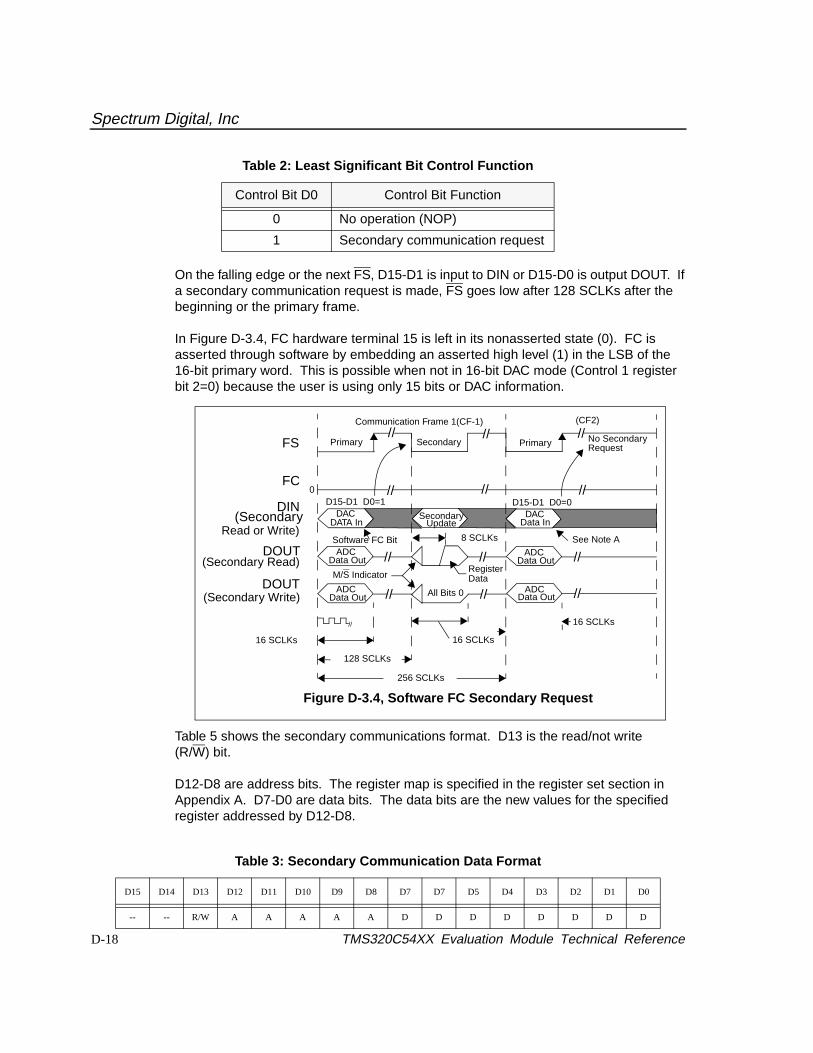
Spectrum Digital, Inc
D-18 TMS320C54XX Evaluation Module Technical Reference
On the falling edge or the next FS, D15-D1 is input to DIN or D15-D0 is output DOUT. Ifa secondary communication request is made, FS goes low after 128 SCLKs after thebeginning or the primary frame.
In Figure D-3.4, FC hardware terminal 15 is left in its nonasserted state (0). FC isasserted through software by embedding an asserted high level (1) in the LSB of the16-bit primary word. This is possible when not in 16-bit DAC mode (Control 1 registerbit 2=0) because the user is using only 15 bits or DAC information.
Table 5 shows the secondary communications format. D13 is the read/not write (R/W) bit.
D12-D8 are address bits. The register map is specified in the register set section inAppendix A. D7-D0 are data bits. The data bits are the new values for the specifiedregister addressed by D12-D8.
Table 2: Least Significant Bit Control Function
Control Bit D0 Control Bit Function
0 No operation (NOP)
1 Secondary communication request
Table 3: Secondary Communication Data Format
D15 D14 D13 D12 D11 D10 D9 D8 D7 D7 D5 D4 D3 D2 D1 D0
-- -- R/W A A A A A D D D D D D D D
FS
FC
DOUT(Secondary Read)
DOUT(Secondary Write)
DIN(Secondary
Read or Write)
16 SCLKs
//////
//
//
//
//
//
//
128 SCLKs
256 SCLKs
16 SCLKs
16 SCLKs
DACDATA In
SecondaryUpdate
DACData In
ADCData Out
ADCData OutAll Bits 0
ADCData Out
ADCData Out
RegisterData
Primary PrimarySecondary
8 SCLKs
No SecondaryRequest
Communication Frame 1(CF-1) (CF2)
M/S Indicator
Figure D-3.4, Software FC Secondary Request
// // //D15-D1 D0=1
0D15-D1 D0=0
//
Software FC Bit See Note A
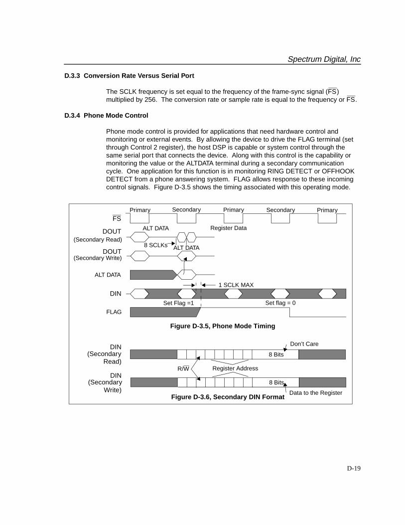
Spectrum Digital, Inc
D-19
D.3.3 Conversion Rate Versus Serial Port
The SCLK frequency is set equal to the frequency of the frame-sync signal (FS)multiplied by 256. The conversion rate or sample rate is equal to the frequency or FS.
D.3.4 Phone Mode Control
Phone mode control is provided for applications that need hardware control and monitoring or external events. By allowing the device to drive the FLAG terminal (setthrough Control 2 register), the host DSP is capable or system control through thesame serial port that connects the device. Along with this control is the capability ormonitoring the value or the ALTDATA terminal during a secondary communicationcycle. One application for this function is in monitoring RING DETECT or OFFHOOKDETECT from a phone answering system. FLAG allows response to these incomingcontrol signals. Figure D-3.5 shows the timing associated with this operating mode.
FS
DOUT(Secondary Read)
DOUT(Secondary Write)
DIN
Figure D-3.5, Phone Mode Timing
ALT DATA
FLAG
Primary Secondary SecondaryPrimary Primary
ALT DATA Register Data
ALT DATA
1 SCLK MAX
Set Flag =1 Set flag = 0
8 SCLKs
DIN(Secondary
Read)
DIN(Secondary
Write)
8 Bits
8 Bits
Register Address
Don’t Care
Data to the Register
R/W
Figure D-3.6, Secondary DIN Format
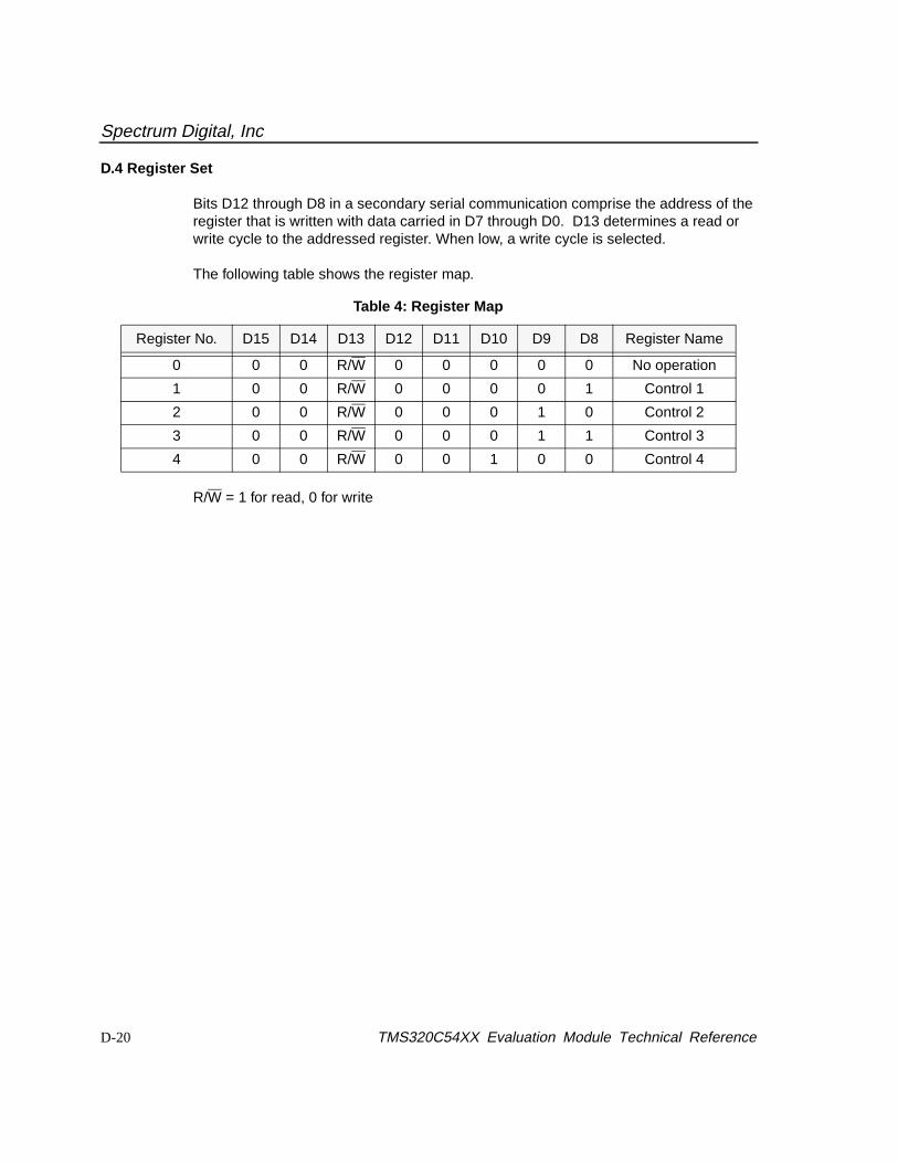
Spectrum Digital, Inc
D-20 TMS320C54XX Evaluation Module Technical Reference
D.4 Register Set
Bits D12 through D8 in a secondary serial communication comprise the address of theregister that is written with data carried in D7 through D0. D13 determines a read orwrite cycle to the addressed register. When low, a write cycle is selected.
The following table shows the register map.
R/W = 1 for read, 0 for write
Table 4: Register Map
Register No. D15 D14 D13 D12 D11 D10 D9 D8 Register Name
0 0 0 R/W 0 0 0 0 0 No operation
1 0 0 R/W 0 0 0 0 1 Control 1
2 0 0 R/W 0 0 0 1 0 Control 2
3 0 0 R/W 0 0 0 1 1 Control 3
4 0 0 R/W 0 0 1 0 0 Control 4

Spectrum Digital, Inc
D-21
D.4.1 Control 1 Register
Default value: 0 0 0 0 0 0 0 0Note 1: These gains are for single ended input. The gain of 6 dB lower with a differential input.
A software reset reset is a one-shot operation and this bit is cleared to 0 after reset. Itis not necessary to write a 0 to end the master reset operation. Writing 0s to thereserved bits is suggested. Writing 0s to the reserved bits is suggested.
Table 5: Control 1 Register
D7 D6 D5 D4 D3 D2 D1 D0 Description
1 - - 0 - - - - Software Reset
0 - - - 0 - - - Software reset not asserted
1 - - - - - - Software power down (analog and filters)
- 0 - - - - - - Software power down (not asserted)
- - 1 - - - - - Select AUXP and AUXM for ADC
- - 0 - - - - - Select INP and INM for ADC
- - - 0 - - - - Select INP and INM for monitor
- - - 1 - - - - Select AUXP and AUXM for ADC
- - - - 1 1 - - Monitor amplifier gain = -18 dB (see note 1)
- - - - 1 0 - - Monitor amplifier gain = -8 dB (see note 1)
- - - - 0 1 - - Monitor amplifier gain = -0 dB (see note 1)
- - - - 0 0 - - Monitor amp mute
- - - - - - 1 - Digital loopback asserted
- - - - - - 0 - Digital loopback not asserted
- - - - - - - 1 16-bit DAC mode (hardware secondary requests)
- - - - - - - 0 Not 16-bit DAC mode (hardware secondary requests)

Spectrum Digital, Inc
D-22 TMS320C54XX Evaluation Module Technical Reference
D.4.2 Control 2 Register
Default: 00000000Writing 0s to the reserved bits is suggested.
D.4.3 Control 3 Register
The following command contains the frame-sync delay (FSD) register address andloads D7 (MSB)-D0 into the FSD register. The data byte (D1-D0) determines thenumber or SCLKs between FS and the delayed frame-sync signal, FSD. The minimumdata value for the register is decimal 18.
Default: 00000000Writing 0s to the reserved bits is suggested.
Table 6: Control 2 Register
D7 D6 D5 D4 D3 D2 D1 D0 Description
X - - 0 - - - - FLAG output value
- 1 - - 0 - - - Phone mode enable
0 - - - - - - Phone mode disable
- 0 X - - - - - Decimator FIR overflow flag (valid only during read cycle)
- - 1 - - - - 16-bit ADC mode
- - 0 0 - - - - Not 16-bit ADC mode
- - - - - X X X Reserved
- - - 1 1 - - - Analog loopback enabled
- - - - 0 - - - Analog loopback disabled
Table 7: Control 3 Register
D7 D6 D5 D4 D3 D2 D1 D0 Description
- - X X X X X X Number of SCLKs between FS and FSD
X X - - - - - - Phone mode enable

Spectrum Digital, Inc
D-23
D.4.4 Control 4 Register
Default value: 00000000The value or the sample frequency divisor, N, is determined by the octal representationor bits D4-D6. Hence, 001 = 1, 010 = 2, etc. By setting D4 - D6 to 000, N = 8 isselected.
Table 8: Control 4 Register
D7 D6 D5 D4 D3 D2 D1 D0 Description
- - - - 1 1 - - Analog input gain = mute
- - - - 1 0 - - Analog input gain = 12 dB
- - - 0 1 - - Analog input gain = 6 dB
- - - - 0 0 - - Analog input gain = 0 dB
- - - - - - 1 1 Analog output gain = mute
- - - - - - 1 0 Analog output gain = -12 dB
- - - - - - 0 1 Analog output gain = -6 dB
- - - - - - 0 0 Analog output gain = 0 dB
- X X X - - - - Samples frequency select (N): fs = MCLK/(128 x N) or MCLK/(512 x N)
1 - - - - - - - External sample clock feature enabled
0 - - - - - - - External sample clock feature disabled

E-1
Appendix E
EVM320 Mechanical Information
This appendix contains the mechanical information about the EVM andWire Wrap Protoype Modules produced by Spectrum Digital.
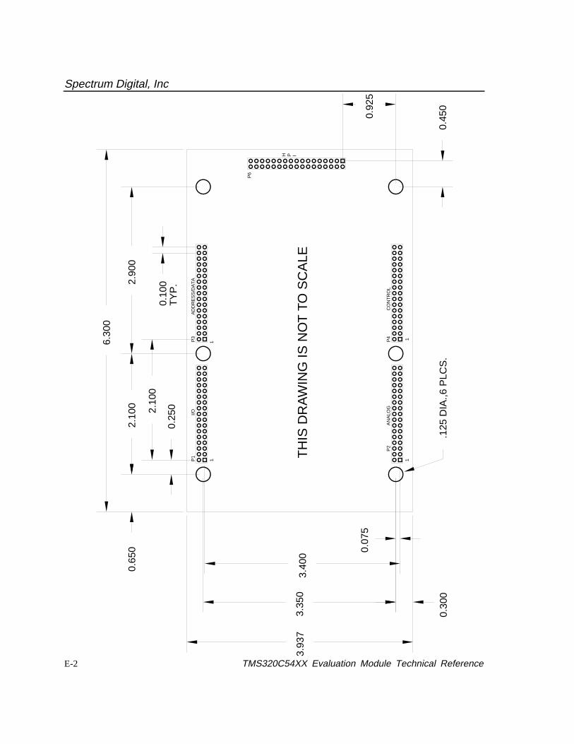
Spectrum Digital, Inc
E-2 TMS320C54XX Evaluation Module Technical Reference
P4
P2
P1
P3
I/OA
DD
RE
SS
/DA
TA
AN
ALO
GC
ON
TR
OL
11
11
3.35
0
.125
DIA
.,6 P
LCS
.
0.07
5
3.40
0
0.30
0
3.93
7
0.65
02.
100 2.10
0
0.25
0
2.90
0
6.30
0
0.10
0T
YP
.
H P I
P6
0.92
5
0.45
0
TH
IS D
RA
WIN
G IS
NO
T T
O S
CA
LE

503482-0001 Rev. IPrinted in U.S.A., March 2001