tms320f20x/f24x dsp embedded flash memory · pdf filethis reference guide describes the...
TRANSCRIPT

TMS320F20x/F24x DSPEmbedded Flash Memory
Technical Reference
This document contains preliminary data current as of publication date and is subject
to change without notice.
Literature Number: SPRU282September 1998
Printed on Recycled Paper

IMPORTANT NOTICE
Texas Instruments and its subsidiaries (TI) reserve the right to make changes to their products or to discontinueany product or service without notice, and advise customers to obtain the latest version of relevant informationto verify, before placing orders, that information being relied on is current and complete. All products are soldsubject to the terms and conditions of sale supplied at the time of order acknowledgement, including thosepertaining to warranty, patent infringement, and limitation of liability.
TI warrants performance of its semiconductor products to the specifications applicable at the time of sale inaccordance with TI’s standard warranty. Testing and other quality control techniques are utilized to the extentTI deems necessary to support this warranty. Specific testing of all parameters of each device is not necessarilyperformed, except those mandated by government requirements.
CERTAIN APPLICATIONS USING SEMICONDUCTOR PRODUCTS MAY INVOLVE POTENTIAL RISKS OFDEATH, PERSONAL INJURY, OR SEVERE PROPERTY OR ENVIRONMENTAL DAMAGE (“CRITICALAPPLICATIONS”). TI SEMICONDUCTOR PRODUCTS ARE NOT DESIGNED, AUTHORIZED, ORWARRANTED TO BE SUITABLE FOR USE IN LIFE-SUPPORT DEVICES OR SYSTEMS OR OTHERCRITICAL APPLICATIONS. INCLUSION OF TI PRODUCTS IN SUCH APPLICATIONS IS UNDERSTOOD TOBE FULLY AT THE CUSTOMER’S RISK.
In order to minimize risks associated with the customer’s applications, adequate design and operatingsafeguards must be provided by the customer to minimize inherent or procedural hazards.
TI assumes no liability for applications assistance or customer product design. TI does not warrant or representthat any license, either express or implied, is granted under any patent right, copyright, mask work right, or otherintellectual property right of TI covering or relating to any combination, machine, or process in which suchsemiconductor products or services might be or are used. TI’s publication of information regarding any thirdparty’s products or services does not constitute TI’s approval, warranty or endorsement thereof.
Copyright 1998, Texas Instruments Incorporated
iii PRELIMINARY
Preface
Read This First
About This Manual
This reference guide describes the operation of the embedded flash EEPROMmodule on the TMS320F20x/F24x digital signal processor (DSP) devices andprovides sample code that you can use in developing your own software. Theperformance specifications of the embedded flash memory have been evalu-ated using the algorithms and techniques described in this guide. TI does notrecommend deviation from these algorithms and techniques, since doing socould affect device performance. The book does not describe the use of anyspecific flash programming tool nor does it describe the external interface tothe DSP. For information about any aspect of the TMS320F20x/F24x devicesother than the embedded flash EEPROM module, see Related Documenta-tion from Texas Instruments on page v.
How to Use This Manual
There are several stand-alone flash programming tools for TMS320F20x/F24x generation of DSPs. Using one of these stand-alone tools with theTMS320F20x/F24x requires only a basic understanding of the flash opera-tions. More information about these flash programming tools is available onthe TI web page, http://www.ti.com. This guide is intended to provide acomplete understanding of the flash operations. This level of understandingis necessary for making modifications to existing flash programming toolsor for developing alternative programming schemes.
If you are looking for in-formation about: Turn to these locations:
Algorithms Chapter 3, Algorithm Implementations andSoftware Considerations
Erasing the flash array Section 1.1, Basic Concepts of Flash MemoryTechnologySection 2.1, Modifying the Contents of theTMS320F20x/F24x Flash ArraySection 2.6, Erase OperationSection 3.3, Erase Algorithm
PRELIMINARY

PRELIMINARY
iv PRELIMINARY
If you are looking for in-formation about: Turn to these locations:
Over-erasure (depletion) andrecovery
Section 1.1, Basic Concepts of Flash MemoryTechnologySection 2.7, Recovering From Over-Erasure(Flash-Write Operation)Section 3.4, Flash-Write Algorithm
Programming the flash array Section 1.1, Basic Concepts of Flash MemoryTechnologySection 2.1, Modifying the Contents of theTMS320F20x/F24x Flash ArraySection 2.5, Program OperationSection 3.2, Programming Algorithm
Sample code Appendix A, Assembly Source Listings andProgram Examples
Notational Conventions
This document uses the following conventions.
� The flash EEPROM is referred to as flash memory or the flash module.The term flash array refers to the actual memory array within the flashmodule. The flash module includes the flash memory array and the associ-ated control circuitry.
� The DSP generation and devices are abbreviated as follows:� TMS320F20x/24x generation: ’F20x/24x� TMS320F20x devices: ’F20x� TMS320F24x devices: ’F24x
� Program listings and code examples are shown in a special type-face .
Here is a sample program listing:
0011 0005 0001 .field 1, 20012 0005 0003 .field 3, 40013 0005 0006 .field 6, 30014 0006 .even

Related Documentation From Texas InstrumentsPRELIMINARY
v Read This FirstPRELIMINARY
Related Documentation From Texas Instruments
The following books describe the ’F20x/24x and related support tools. To ob-tain a copy of any of these TI documents, call the Texas Instruments LiteratureResponse Center at (800) 477–8924. When ordering, please identify the bookby its title and literature number.
TMS320C24x DSP Controllers Reference Set, Volume 1: CPU, System,and Instruction Set (literature number SPRU160) describes theTMS320C24x 16-bit, fixed-point, digital signal processor controller.Covered are its architecture, internal register structure, data andprogram addressing, and instruction set. Also includes instruction setcomparisons and design considerations for using the XDS510 emulator.
TMS320C24x DSP Controllers Reference Set Volume 2: PeripheralLibrary and Specific Devices (literature number SPRU161) describesthe peripherals available on the TMS320C24x digital signal processorcontrollers and their operation. Also described are specific deviceconfigurations of the ’C24x family.
TMS320C240, TMS320F240 DSP Controllers (literature number SPRS042)data sheet contains the electrical and timing specifications for thesedevices, as well as signal descriptions and pinouts for all of the availablepackages.
TMS320C2x/C2xx/C5x Optimizing C Compiler User’s Guide (literaturenumber SPRU024) describes the ’C2x/C2xx/C5x C compiler. This Ccompiler accepts ANSI standard C source code and produces TMS320assembly language source code for the ’C2x, ’C2xx, and ’C5x genera-tions of devices.
TMS320F206 Digital Signal Processor (literature number SPRS050) datasheet contains the electrical and timing specifications for the ’F206device, as well as signal descriptions and the pinout.
TMS320F241, TMS320C241, TMS320C242 DSP Controllers (literaturenumber SPRS063) data sheet contains the electrical and timingspecifications for the ’F241, ’C241, and ’C242 devices, as well as signaldescriptions and pinouts.
TMS320F243 DSP Controller (literature number SPRS064) data sheetcontains the electrical and timing specifications for the ’F243 device, aswell as signal descriptions and the pinout.
TMS320C2xx User’s Guide (literature number SPRU127) discusses thehardware aspects of the ’C2xx 16-bit, fixed-point digital signal proces-sors. It describes the architecture, the instruction set, and the on-chip pe-ripherals.
Related Documentation From Texas Instruments PRELIMINARY
vi PRELIMINARY
TMS320C2xx C Source Debugger User’s Guide (literature numberSPRU151) tells you how to invoke the ’C2xx emulator and simulator ver-sions of the C source debugger interface. This book discusses variousaspects of the debugger interface, including window management, com-mand entry, code execution, data management, and breakpoints. It alsoincludes a tutorial that introduces basic debugger functionality.

If You Need Assistance . . .PRELIMINARY
vii Read This FirstPRELIMINARY
If You Need Assistance . . .
� World-Wide Web SitesTI Online http://www.ti.comSemiconductor Product Information Center (PIC) http://www.ti.com/sc/docs/pic/home.htmDSP Solutions http://www.ti.com/dsps320 Hotline On-line� http://www.ti.com/sc/docs/dsps/support.htm
� North America, South America, Central AmericaProduct Information Center (PIC) (972) 644-5580TI Literature Response Center U.S.A. (800) 477-8924Software Registration/Upgrades (214) 638-0333 Fax: (214) 638-7742U.S.A. Factory Repair/Hardware Upgrades (281) 274-2285U.S. Technical Training Organization (972) 644-5580DSP Hotline (281) 274-2320 Fax: (281) 274-2324 Email: [email protected] Modem BBS (281) 274-2323DSP Internet BBS via anonymous ftp to ftp://ftp.ti.com/pub/tms320bbs
� Europe, Middle East, AfricaEuropean Product Information Center (EPIC) Hotlines:
Multi-Language Support +33 1 30 70 11 69 Fax: +33 1 30 70 10 32Email: [email protected]
Deutsch +49 8161 80 33 11 or +33 1 30 70 11 68English +33 1 30 70 11 65Francais +33 1 30 70 11 64Italiano +33 1 30 70 11 67
EPIC Modem BBS +33 1 30 70 11 99European Factory Repair +33 4 93 22 25 40Europe Customer Training Helpline Fax: +49 81 61 80 40 10
� Asia-PacificLiterature Response Center +852 2 956 7288 Fax: +852 2 956 2200Hong Kong DSP Hotline +852 2 956 7268 Fax: +852 2 956 1002Korea DSP Hotline +82 2 551 2804 Fax: +82 2 551 2828Korea DSP Modem BBS +82 2 551 2914Singapore DSP Hotline Fax: +65 390 7179Taiwan DSP Hotline +886 2 377 1450 Fax: +886 2 377 2718Taiwan DSP Modem BBS +886 2 376 2592Taiwan DSP Internet BBS via anonymous ftp to ftp://dsp.ee.tit.edu.tw/pub/TI/
� JapanProduct Information Center +0120-81-0026 (in Japan) Fax: +0120-81-0036 (in Japan)
+03-3457-0972 or (INTL) 813-3457-0972 Fax: +03-3457-1259 or (INTL) 813-3457-1259DSP Hotline +03-3769-8735 or (INTL) 813-3769-8735 Fax: +03-3457-7071 or (INTL) 813-3457-7071DSP BBS via Nifty-Serve Type “Go TIASP”
� DocumentationWhen making suggestions or reporting errors in documentation, please include the following information that is on the titlepage: the full title of the book, the publication date, and the literature number.
Mail: Texas Instruments Incorporated Email: [email protected] Documentation Services, MS 702P.O. Box 1443Houston, Texas 77251-1443
Note: When calling a Literature Response Center to order documentation, please specify the literature number of thebook.

Contents
ix
Contents
1 Introduction 1�1. . . . . . . . . . . . . . . . . . . . . . . . . . . . . . . . . . . . . . . . . . . . . . . . . . . . . . . . . . . . . . . . . . . . . Discusses basic flash memory technology; summarizes the features and benefits of theTMS320F20x/F24x flash module
1.1 Basic Concepts of Flash Memory Technology 1�2. . . . . . . . . . . . . . . . . . . . . . . . . . . . . . . . . . 1.2 TMS320F20x/F24x Flash Module 1�3. . . . . . . . . . . . . . . . . . . . . . . . . . . . . . . . . . . . . . . . . . . . . 1.3 Benefits of Embedded Flash Memory in a DSP System 1�5. . . . . . . . . . . . . . . . . . . . . . . . . .
2 Flash Operations and Control Registers 2 �1. . . . . . . . . . . . . . . . . . . . . . . . . . . . . . . . . . . . . . . . . . Describes the operations that modify the content of the flash module; explains the role of thecontrol registers
2.1 Operations that Modify the Contents of the ’F20x/F24x Flash Array 2�2. . . . . . . . . . . . . . . 2.2 Accessing the Flash Module 2�5. . . . . . . . . . . . . . . . . . . . . . . . . . . . . . . . . . . . . . . . . . . . . . . . .
2.2.1 TMS320F206 Flash Access-Control Register 2�6. . . . . . . . . . . . . . . . . . . . . . . . . . . 2.2.2 TMS320F24x Flash Access-Control Register 2�7. . . . . . . . . . . . . . . . . . . . . . . . . . . .
2.3 Flash Module Control Registers 2�8. . . . . . . . . . . . . . . . . . . . . . . . . . . . . . . . . . . . . . . . . . . . . . 2.3.1 Segment Control Register (SEG_CTR) 2�8. . . . . . . . . . . . . . . . . . . . . . . . . . . . . . . . . 2.3.2 Flash Test Register (TST) 2�10. . . . . . . . . . . . . . . . . . . . . . . . . . . . . . . . . . . . . . . . . . . 2.3.3 Write Address Register (WADRS) 2�10. . . . . . . . . . . . . . . . . . . . . . . . . . . . . . . . . . . . 2.3.4 Write Data Register (WDATA) 2�11. . . . . . . . . . . . . . . . . . . . . . . . . . . . . . . . . . . . . . . .
2.4 Read Modes 2�12. . . . . . . . . . . . . . . . . . . . . . . . . . . . . . . . . . . . . . . . . . . . . . . . . . . . . . . . . . . . . . 2.5 Program Operation 2�13. . . . . . . . . . . . . . . . . . . . . . . . . . . . . . . . . . . . . . . . . . . . . . . . . . . . . . . . 2.6 Erase Operation 2�14. . . . . . . . . . . . . . . . . . . . . . . . . . . . . . . . . . . . . . . . . . . . . . . . . . . . . . . . . . . 2.7 Recovering From Over-Erasure (Flash-Write Operation) 2�15. . . . . . . . . . . . . . . . . . . . . . . . 2.8 Reading From the Flash Array 2�16. . . . . . . . . . . . . . . . . . . . . . . . . . . . . . . . . . . . . . . . . . . . . . . 2.9 Protecting the Array 2�16. . . . . . . . . . . . . . . . . . . . . . . . . . . . . . . . . . . . . . . . . . . . . . . . . . . . . . . .
3 Algorithm Implementations and Software Considerations 3 �1. . . . . . . . . . . . . . . . . . . . . . . . . . Describes the algorithms used for the programming, erase, and flash-write operations; dis-cusses considerations necessary for developing your software
3.1 How the Algorithms Fit Into the Program-Erase-Reprogram Flow 3�2. . . . . . . . . . . . . . . . . 3.2 Programming (or Clear) Algorithm 3�4. . . . . . . . . . . . . . . . . . . . . . . . . . . . . . . . . . . . . . . . . . . . 3.3 Erase Algorithm 3�10. . . . . . . . . . . . . . . . . . . . . . . . . . . . . . . . . . . . . . . . . . . . . . . . . . . . . . . . . . . 3.4 Flash-Write Algorithm 3�14. . . . . . . . . . . . . . . . . . . . . . . . . . . . . . . . . . . . . . . . . . . . . . . . . . . . . .
A Assembly Source Listings and Program Examples A �1. . . . . . . . . . . . . . . . . . . . . . . . . . . . . . . . . A.1 Assembly Source for Algorithms A�2. . . . . . . . . . . . . . . . . . . . . . . . . . . . . . . . . . . . . . . . . . . . . .

Contents
x
A.1.1 Header File for Constants and Variables, SVAR20.H A�2. . . . . . . . . . . . . . . . . . . . . A.1.2 Clear Algorithm, SCLR20.ASM A�5. . . . . . . . . . . . . . . . . . . . . . . . . . . . . . . . . . . . . . . . A.1.3 Erase Algorithm, SERA20.ASM A�10. . . . . . . . . . . . . . . . . . . . . . . . . . . . . . . . . . . . . . A.1.4 Flash-Write Algorithm, SFLW20.ASM A�15. . . . . . . . . . . . . . . . . . . . . . . . . . . . . . . . . A.1.5 Programming Algorithm, SPGM20.ASM A�19. . . . . . . . . . . . . . . . . . . . . . . . . . . . . . . A.1.6 Subroutines Used By All Four Algorithms, SUTILS20.ASM A�25. . . . . . . . . . . . . . .
A.2 C-Callable Interface to Flash Algorithms A�27. . . . . . . . . . . . . . . . . . . . . . . . . . . . . . . . . . . . . . A.3 Sample Assembly Code to Erase and Reprogram the TMS320F206 A�32. . . . . . . . . . . . . .
A.3.1 Assembly Code for TMS320F206 A�32. . . . . . . . . . . . . . . . . . . . . . . . . . . . . . . . . . . . . A.3.2 Linker Command File for TMS320F206 Sample Assembly Code A�35. . . . . . . . . .
A.4 Sample C Code to Erase and Reprogram the TMS320F206 A�37. . . . . . . . . . . . . . . . . . . . . A.4.1 C Code That Calls the Interface to Flash Algorithms for TMS320F206 A�37. . . . . A.4.2 Linker Command File for TMS320F206 Sample C Code A�38. . . . . . . . . . . . . . . . .
A.5 Sample Assembly Code to Erase and Reprogram the TMS320F240 A�40. . . . . . . . . . . . . . A.5.1 Assembly Code for TMS320F240 A�40. . . . . . . . . . . . . . . . . . . . . . . . . . . . . . . . . . . . . A.5.2 Linker Command File for TMS320F240 Sample Assembly Code A�45. . . . . . . . . .
A.6 Using the Algorithms With C Code to Erase and Reprogram the ’F240 A�47. . . . . . . . . . . . A.6.1 C Code That Calls the Interface to Flash Algorithms for TMS320F240 A�47. . . . . A.6.2 Linker Command File for TMS320F240 Sample C Code A�48. . . . . . . . . . . . . . . . . A.6.3 C Function for Disabling TMS320F240 Watchdog Timer A�50. . . . . . . . . . . . . . . . . A.6.4 C Functions for Initializing the TMS320F240 A�51. . . . . . . . . . . . . . . . . . . . . . . . . . .

Figures
xiContents
Figures
1–1 TMS320F20x/F24x Program Space Memory Maps 1�4. . . . . . . . . . . . . . . . . . . . . . . . . . . . . . . . 2–1 Flash Memory Logic Levels During Programming and Erasing 2�4. . . . . . . . . . . . . . . . . . . . . . 2–2 Memory Maps in Register and Array Access Modes 2�6. . . . . . . . . . . . . . . . . . . . . . . . . . . . . . . 2–3 Segment Control Register (SEG_CTR) 2�8. . . . . . . . . . . . . . . . . . . . . . . . . . . . . . . . . . . . . . . . . . 3–1 Algorithms in the Overall Flow 3�3. . . . . . . . . . . . . . . . . . . . . . . . . . . . . . . . . . . . . . . . . . . . . . . . . . 3–2 The Programming Algorithm in the Overall Flow 3�4. . . . . . . . . . . . . . . . . . . . . . . . . . . . . . . . . . . 3–3 Programming or Clear Algorithm Flow 3-6. . . . . . . . . . . . . . . . . . . . . . . . . . . . . . . . . . . . . . . . . . . 3–4 Erase Algorithm in the Overall Flow 3�10. . . . . . . . . . . . . . . . . . . . . . . . . . . . . . . . . . . . . . . . . . . . 3–5 Erase Algorithm Flow 3�13. . . . . . . . . . . . . . . . . . . . . . . . . . . . . . . . . . . . . . . . . . . . . . . . . . . . . . . . . 3–6 Flash-Write Algorithm in the Overall Flow 3�14. . . . . . . . . . . . . . . . . . . . . . . . . . . . . . . . . . . . . . . 3–7 Flash-Write Algorithm Flow 3�16. . . . . . . . . . . . . . . . . . . . . . . . . . . . . . . . . . . . . . . . . . . . . . . . . . . .
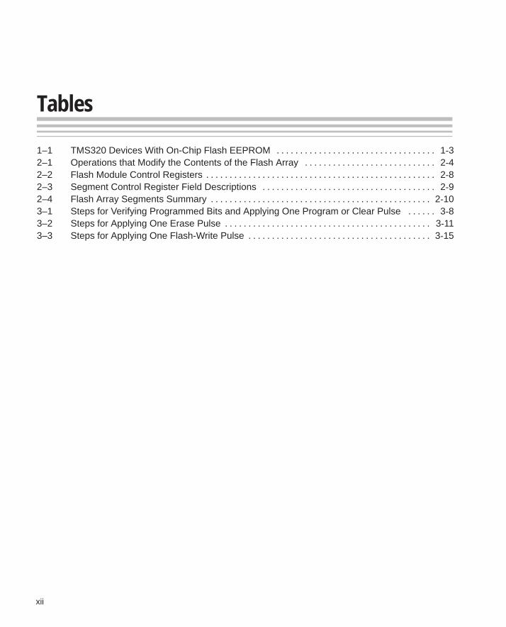
Tables
xii
Tables
1–1 TMS320 Devices With On-Chip Flash EEPROM 1�3. . . . . . . . . . . . . . . . . . . . . . . . . . . . . . . . . . 2–1 Operations that Modify the Contents of the Flash Array 2�4. . . . . . . . . . . . . . . . . . . . . . . . . . . . 2–2 Flash Module Control Registers 2�8. . . . . . . . . . . . . . . . . . . . . . . . . . . . . . . . . . . . . . . . . . . . . . . . . 2–3 Segment Control Register Field Descriptions 2�9. . . . . . . . . . . . . . . . . . . . . . . . . . . . . . . . . . . . . 2–4 Flash Array Segments Summary 2�10. . . . . . . . . . . . . . . . . . . . . . . . . . . . . . . . . . . . . . . . . . . . . . . 3–1 Steps for Verifying Programmed Bits and Applying One Program or Clear Pulse 3�8. . . . . . 3–2 Steps for Applying One Erase Pulse 3�11. . . . . . . . . . . . . . . . . . . . . . . . . . . . . . . . . . . . . . . . . . . . 3–3 Steps for Applying One Flash-Write Pulse 3�15. . . . . . . . . . . . . . . . . . . . . . . . . . . . . . . . . . . . . . .

1-1
Introduction
The TMS320F20x/F24x digital signal processors (DSPs) contain on-chip flashEEPROM (electrically-erasable programmable read-only memory). The em-bedded flash memory provides an attractive alternative to masked programROM. Like ROM, flash memory is nonvolatile, but it has an advantage overROM: in-system reprogrammability.
This chapter discusses basic flash memory technology, introduces the flashmemory module of the ’F20x/F24x DSP, and lists the benefits of flash memoryembedded in a DSP chip.
Topic Page
1.1 Basic Concepts of Flash Memory Technology 1-2. . . . . . . . . . . . . . . . . . .
1.2 TMS320F20x/F24x Flash Module 1-3. . . . . . . . . . . . . . . . . . . . . . . . . . . . . . .
1.3 Benefits of Embedded Flash Memory in a DSP System 1-5. . . . . . . . . . .
Chapter 1
PRELIMINARY
PRELIMINARY
Basic Concepts of Flash Memory Technology PRELIMINARY
1-2 PRELIMINARY
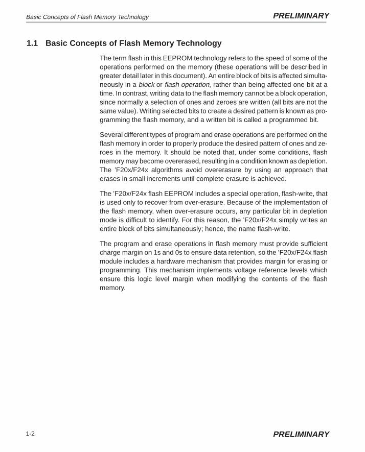
1.1 Basic Concepts of Flash Memory Technology
The term flash in this EEPROM technology refers to the speed of some of theoperations performed on the memory (these operations will be described ingreater detail later in this document). An entire block of bits is affected simulta-neously in a block or flash operation, rather than being affected one bit at atime. In contrast, writing data to the flash memory cannot be a block operation,since normally a selection of ones and zeroes are written (all bits are not thesame value). Writing selected bits to create a desired pattern is known as pro-gramming the flash memory, and a written bit is called a programmed bit.
Several different types of program and erase operations are performed on theflash memory in order to properly produce the desired pattern of ones and ze-roes in the memory. It should be noted that, under some conditions, flashmemory may become overerased, resulting in a condition known as depletion.The ’F20x/F24x algorithms avoid overerasure by using an approach thaterases in small increments until complete erasure is achieved.
The ’F20x/F24x flash EEPROM includes a special operation, flash-write, thatis used only to recover from over-erasure. Because of the implementation ofthe flash memory, when over-erasure occurs, any particular bit in depletionmode is difficult to identify. For this reason, the ’F20x/F24x simply writes anentire block of bits simultaneously; hence, the name flash-write.
The program and erase operations in flash memory must provide sufficientcharge margin on 1s and 0s to ensure data retention, so the ’F20x/F24x flashmodule includes a hardware mechanism that provides margin for erasing orprogramming. This mechanism implements voltage reference levels whichensure this logic level margin when modifying the contents of the flashmemory.

TMS320F20x/F24x Flash ModulePRELIMINARY
1-3IntroductionPRELIMINARY
1.2 TMS320F20x/F24x Flash Module
The ’F20x/F24x flash EEPROM is implemented with one or two independentflash memory modules of 8K or 16K words. Each flash module is composedof a flash memory array, four control registers, and circuitry that produces ana-log voltages for programming and erasing. The flash array size of theTMS320F206 and TMS320F240 is 16K × 16 bits, while the TMS320F241 andTMS320F243 incorporate an 8K × 16-bit flash array (see Table 1–1). Unlikemost discrete flash memories, the ’F20x/F24x flash module does not requirea dedicated state machine, because the algorithms for programming and eras-ing the flash are executed in software by the DSP core. The use of these so-phisticated, adaptive programming algorithms results in reduced chip size andgreater programming flexibility. In addition, the application code can managethe use of the flash memory without the requirement of external programmingequipment.
Table 1–1. TMS320 Devices With On-Chip Flash EEPROM
Device Array Size Total Flash Memory
TMS320F206 16K 32K†
TMS320F240 16K 16K
TMS320F241 8K 8K
TMS320F243 8K 8K
† Each array can be independently erased.
TMS320F20x/F24x Flash Module PRELIMINARY
1-4 PRELIMINARY
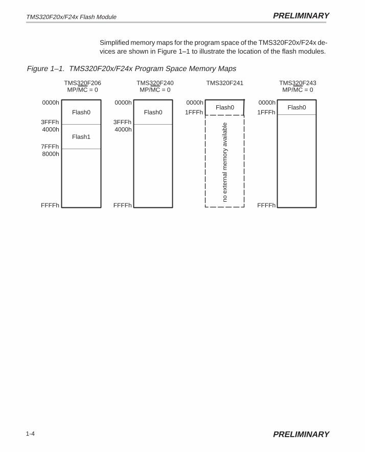
Simplified memory maps for the program space of the TMS320F20x/F24x de-vices are shown in Figure 1–1 to illustrate the location of the flash modules.
Figure 1–1. TMS320F20x/F24x Program Space Memory Maps
0000h
1FFFh
FFFFh
Flash0
TMS320F241
Flash00000h
1FFFhFlash0
4000h3FFFh
0000h
FFFFhFFFFh
8000h7FFFh
4000h3FFFh
0000h
Flash1
Flash0
TMS320F243MP/MC = 0
TMS320F240MP/MC = 0
TMS320F206MP/MC = 0
no e
xter
nal m
emor
y av
aila
ble

Benefits of Embedded Flash Memory in a DSP SystemPRELIMINARY
1-5IntroductionPRELIMINARY
1.3 Benefits of Embedded Flash Memory in a DSP System
The circuitry density of flash memory is about half that of conventional EE-PROM memory, making it possible to approach DRAM densities with flashmemory. This increased density allows flash memory to be integrated with aCPU and other peripherals in a single ’F20x/F24x DSP chip. Embedded flashmemory expands the capabilities of the ’F20x/F24x DSPs in the areas of proto-typing, integrated solutions, and field upgradeable designs.
Embedded flash memory facilitates system development and early field test-ing. Throughout the development process, the system software can be up-dated and reprogrammed into the flash memory for testing at various stages.Since flash is a non-volatile memory type, the resulting standalone prototypecan be tested in the appropriate environment without the need for batterybackup. In addition to its nonvolatile nature, embedded flash memory has theadvantage of in-system programming. Unlike some discrete flash or EEPROMchips, embedded flash memory can be programmed without removing the de-vice from the system board. In fact, the embedded flash memory of ’F20x/F24xDSPs can be programmed using hardware emulators which are already an in-tegral part of the DSP development process; no external programming equip-ment is required.
The embedded flash memory of ’F20x/F24x DSPs also makes these devicesideal for highly integrated, low-cost systems. The initial investment involvedwith making a ROM memory is not justifiable for certain low-cost applications.Accordingly, when on-chip ROM is not an option, DSP system designers usu-ally resort to using expensive static RAM (SRAM), to store system softwareand data. The SRAM provides the fast access times required by the DSP, buthas the disadvantage of being a volatile memory type. To address the issueof memory volatility, designers often use a low-cost EPROM or flash device toload the SRAM after system power-up. This approach is very expensive, andthe increased chip count is often prohibitive. The ’F20x/F24x DSPs, with theiron-chip flash memory modules, provide a single chip solution with nonvolatilememory that supports full speed DSP access rates.
Another benefit of embedded flash memory in a DSP system is remote repro-grammability. Field upgradeability is an extremely useful feature for em-bedded systems. For example, many modem manufacturers offer algorithmupgrades remotely, without requiring the modem to be removed from the hostcomputer system. The same type of feature is also being offered for manyhandheld consumer products. Adding this capability to a product requires theaddition of EEPROM or flash devices, which increase chip count and systemcost. Since no external equipment is required to program the embedded flashmemory of the ’F20x/F24x DSPs, these devices enable field upgradeabilitywithout impacting system cost.
2-1
Flash Operations and Control Registers
The operations that modify the contents of the ’F20x/F24x flash array are per-formed in software through the use of dedicated programming algorithms. Thischapter introduces the operations performed by these algorithms and explainsthe role of the control registers in this process. The actual algorithms are dis-cussed in Chapter 3.
Topic Page
2.1 Operations that Modify the Contents of the ’F20x/F24x Flash Array 2-2. . . . . . . . . . . . . . . . . . . . . . . . . . . . . . . . . . . . . . . . . . . . . . . . . . .
2.2 Accessing the Flash Module 2-5. . . . . . . . . . . . . . . . . . . . . . . . . . . . . . . . . . .
2.3 Flash Module Control Registers 2-8. . . . . . . . . . . . . . . . . . . . . . . . . . . . . . . .
2.4 Read Modes 2-12. . . . . . . . . . . . . . . . . . . . . . . . . . . . . . . . . . . . . . . . . . . . . . . . .
2.5 Program Operation 2-13. . . . . . . . . . . . . . . . . . . . . . . . . . . . . . . . . . . . . . . . . . .
2.6 Erase Operation 2-14. . . . . . . . . . . . . . . . . . . . . . . . . . . . . . . . . . . . . . . . . . . . .
2.7 Recovering From Over-Erasure (Flash-Write Operation) 2-15. . . . . . . . .
2.8 Reading From the Flash Array 2-16. . . . . . . . . . . . . . . . . . . . . . . . . . . . . . . .
2.9 Protecting the Array 2-16. . . . . . . . . . . . . . . . . . . . . . . . . . . . . . . . . . . . . . . . . .
Chapter 2
PRELIMINARY
PRELIMINARY

Operations that Modify the Contents of the ’F20x/F24x Flash Array PRELIMINARY
2-2 PRELIMINARY
2.1 Operations that Modify the Contents of the ’F20x/F24x Flash Array
Operations that modify the contents of the flash array are generically referredto as either “programming,” which drives one or more bits toward the logic zerostate, or “erasing,” which drives all bits towards the logic one state. It shouldbe noted that since these operations are performed incrementally, a single“programming” or “erasing” operation does not ALWAYS result in a valid logicone or zero. The result of each of these types of operations depends on theinitial state of the bit(s) prior to the operation. This is described in more detailbelow.
Within these two basic types of operations (which are related to the fact thatthere are only two valid logic levels in the F20x/F24x device) are four distinctlydifferent types of functions which are actually performed.
In the category of “programming” operations, there are three actual types offunctions that are performed:
� Clear – which is used to write ALL array bits to a zero state,
� Program – which is used to write SELECTED array bits to zero, and
� Flash-Write – which is used to recover ALL array bits from depletion
In the category of “erase” operations, there is only one type of operation:
� Erase – which is used to write ALL array bits to a one state.
Clear, Program, Flash-Write, and Erase are the only four functions that areused to modify the flash array.
Assuming that the intent of a modification of the contents of the flash array isto program the array with a selection of ones and zeroes, the following se-quence of operations must be performed for proper operation of the flashmemory:
1) The array is first CLEARED to all zeroes.
2) The array is then ERASED to all ones.
3) The array is then checked for depletion and recovered using FLASH-WRITE if necessary (note that if Flash-Write is used to recover from deple-tion, this sequence must be started over again with the Clear and Erasefunctions).
4) Once the array is properly cleared and erased, and verified not to be indepletion, the array is then PROGRAMMED with the desired selection ofzero bits.

Operations that Modify the Contents of the ’F20x/F24x Flash ArrayPRELIMINARY
2-3 Flash Operations and Control RegistersPRELIMINARY
This procedure is discussed in complete detail in Chapter 3.
During these operations that are used to modify the contents of the flash array,three special read modes, and a corresponding set of reference voltage levels,are used when reading back data values to verify programming and erase op-erations.
These read modes and reference levels are:
� VER0 – which is used to verify the logic zero level including margin,
� VER1 – which is used to verify the logic one level including margin, and
� Inverse Erase – which is used to verify depletion recovery.
These concepts are illustrated graphically in Figure 2–1 and summarized inTable 2–1.
Note that ONLY the Erase and the Flash-Write functions are truly “flash” in thesense that these functions actually affect all bits in the array simultaneously.In contrast, bit programming levels in the Program and Clear functions can becontrolled individually on a bit-by-bit basis.
Therefore, when using the Erase or Flash-Write functions, the whole array ismodified, and then the whole array is read, word by word, to verify whether allwords have reached the same value (if not, further iterations of the Erase orFlash-Write functions continue).
In these cases, as mentioned previously, all the bits in the array are modifiedsimultaneously, but some bits may react more quickly, potentially resulting invariation in actual levels on different bits. Therefore, when performing anErase, it is possible that some bits may reach depletion even before other bitsreach the logic one reference level (VER1).
The reason that it is critical to clear the array to a consistent zero level beforeerasing the array is to give maximum immunity to depletion when erasing.Note, however, that even when following this sequence, some flash arraysmay experience depletion, and may require recovery using the Flash-Writefunction.
In contrast to the true “flash” operations Erase and Flash-Write, after each in-cremental Program or Clear operation, each bit is tested against the VER0 ref-erence level to determine the exact point at which it has reached the propervalue, following which, no further incremental adjustment of the level is madeon that bit. Therefore, when the Program or Clear operation is complete, all bitsare at the same zero level, which greatly increases proper data retention anddepletion immunity for the device. Again, note that the programming and eraseoperations are discussed in complete detail in Chapter 3.

Operations that Modify the Contents of the ’F20x/F24x Flash Array PRELIMINARY
2-4 PRELIMINARY
Figure 2–1. Flash Memory Logic Levels During Programming and Erasing
Erase operation
Depletion Mode
Logic 1
1 Margin
0 Margin
Logic 0
VER0
Erase
(Towards logic
Clear
Program
Flash Write
(Towards logic
Referencelevel
Inverse Erase
Program operations
Reference LevelVER1
�
�
�
�
Reference Level
one level)
zero level)
Table 2–1. Operations that Modify the Contents of the Flash Array
Change in Bit Level
Towards Logic 1 Towards Logic 0
Function Reference Level
Function Reference Level
Erase (all bits) VER1 Program (selected bits) VER0
Clear (all bits) VER0
Flash-Write (all bits) Inverse Erase

Accessing the Flash ModulePRELIMINARY
2-5 Flash Operations and Control RegistersPRELIMINARY
2.2 Accessing the Flash Module
In addition to the flash memory array, each flash module has four registers thatcontrol operations on the flash array. These registers are:
� Segment control register (SEG_CTR)
� Test register (TST)
� Write address register (WADRS)
� Write data register (WDATA)
The flash module operates in one of two modes: one in which the flash memoryis accessed directly by the CPU, and one in which the memory array cannotbe accessed directly, but the four control registers are accessible. This modeis used for programming. Each flash module has a flash access-control regis-ter that selects between these two access modes. The register is a single-bit,I/O-mapped register.
The two access modes are summarized as follows:
� Array-access mode. You can access the flash array in the memory spacedecoded for the flash module. The flash module remains in this mode mostof the time, because it allows the DSP core to read from the memory array.
� Register-access mode. You can access the four control registers in thememory space decoded for the flash module. This mode is used for pro-gramming. When the flash module is in register-access mode, the regis-ters are repeated every four address locations within the flash module’saddress range.
The flash array is not directly accessible as memory in register-access mode,and the control registers are not directly accessible in array-access mode.
Figure 2–2 shows memory maps of the flash array in register and array accessmodes.

Accessing the Flash Module PRELIMINARY
2-6 PRELIMINARY
Figure 2–2. Memory Maps in Register and Array Access Modes
SEG_CTR register
TST register
WADRS register
WDATA register
Flash memoryarray
Flash access control register(single bit)
MODE = 1: Array-access modeMODE = 0: Register access mode
0100 ... 010
0100 ... 011
1110 ...110
0110 ...111
4 registers duplicated
4 registers duplicated
4 registers duplicated
2.2.1 TMS320F206 Flash Access-Control Register
Because each flash module has an access-control register associated with it,the ’F206 has two access-control registers. These registers are standard I/O-mapped registers that can be read with an IN instruction and must be modifiedwith an OUT instruction.
� F_ACCESS0 is mapped in I/O space at 0FFE0h.� F_ACCESS1 is mapped in I/O space at 0FFE1h.
The MODE bit (bit 0) of the access-control register selects the access mode:
MODE = 0 Register-access mode
MODE = 1 Array-access mode
Bits 15–1 of each access-control register are always read as 0 and are unaf-fected by writes.

Accessing the Flash ModulePRELIMINARY
2-7 Flash Operations and Control RegistersPRELIMINARY
Although the function is the same, the access control registers of the ’F206 de-vice are mapped at different addresses from that of the ’F24x devices, andtheir values are modified in a different way.
2.2.2 TMS320F24x Flash Access-Control Register
The access-control register of the ’F24x devices is a special type of I/O-mapped register that cannot be read. The register is mapped at I/O address0FF0Fh, and it functions as indicated below.
Note:
For both the IN and OUT instructions, the data operand (dummy) is not used,and can be any valid memory location.
An OUT instruction using the register address as an I/O port places the flashmodule in register-access mode.
For example:
OUT dummy, 0FF0Fh ;Selects register-access mode
An IN instruction using the register address as an I/O port places the flashmodule in array-access mode.
The data operand (dummy) is not used, and can be any valid memory location.
For example:
IN dummy, 0FF0Fh ;Selects array-access mode

Flash Module Control Registers PRELIMINARY
2-8 PRELIMINARY
2.3 Flash Module Control Registers
Table 2–2 lists the control registers and their relative addresses within the fourlocations that repeat throughout the module’s address range.
Table 2–2. Flash Module Control Registers
Relative RegisterDescribed in ...
RelativeAddress
RegisterName Description Section Page
0 SEG_CTR Segment control register. The eight MSBs enable spe-cific segments for programming. Setting a bit to 1 en-ables the segment. The eight LSBs control the pro-gram, erase, and verify operations of the module.
2.3.1 2-5
1 TST Test register. Reserved for test; not accessible to theuser.
2.3.2 2-8
2 WADRS Write address register. Holds the address for a writeoperation.
2.3.3 2-8
3 WDATA Write data register. Holds the data for a write operation. 2.3.4 2-8
2.3.1 Segment Control Register (SEG_CTR)
SEG_CTR is a 16-bit register that initiates and monitors the programming anderasing of the flash array. This register contains the bits that initiate the activeoperations (the WRITE/ERASE field and EXE bit), those used for verification(VER0 and VER1), and those used for protection (KEY0, KEY1, andSEG7–SEG0). All bits of SEG_CTR register are cleared to 0 upon reset.
SEG_CTR is shown in Figure 2–3 and the fields are described in Table 2–3.
Figure 2–3. Segment Control Register (SEG_CTR)
15 14 13 12 11 10 9 8 7 6 5 4 3 2 1 0
SEG7 SEG6 SEG5 SEG4 SEG3 SEG2 SEG1 SEG0 Res KEY1 KEY0 VER0 VER1 WRITE/ERASE EXE
RW–0 RW–0 RW–0 RW–0 RW–0 RW–0 RW–0 RW–0 X RW–0 RW–0 RW–0 RW–0 RW–0 RW–0
Legend: R = readW = write–0 = value after resetX = don’t care

Flash Module Control RegistersPRELIMINARY
2-9 Flash Operations and Control RegistersPRELIMINARY
Table 2–3. Segment Control Register Field Descriptions
Bits Name Description
15–8 SEG7–SEG0 Segment enable bits. Each of these bits protects the specified segment against pro-gramming or enables programming for the specified segment in the array. Any numberof segments (from 0 to 7 in any combination) can be enabled at any one time. SeeTable 2–4 for segment address ranges. EXE must be cleared to modify the SEGx bits.
SEGx = 1 enables programming of the corresponding segment.SEGx = 0 protects the segment from programming.
7 Reserved This bit is not affected by writes, and reads of this bit are undefined.
6–5 KEY1, KEY0 Execute key bits. A binary value of 10 must be written to these bits in the same DSPcore access in which the EXE bit is set for the selected operation (erase, program, orflash-write) to start. KEY1 and KEY0 must be cleared in the same write access thatclears EXE. These bits are used as additional protection against inadvertent program-ming or erasure of the array. These bits are read as 0s.
4–3 VER0, VER1 Verify bits. These bits select special read modes used to verify proper erasure or pro-gramming.
Possible values:
00: Normal read mode01: Verify 1s (VER1) read mode to verify margin of 1s for proper erasure10: Verify 0s (VER0) read mode to verify margin of 0s for proper programming11: Inverse-read mode; tests for bits erased into depletion
2–1 WRITE/ERASE Write/erase enable field. These bits select the program, erase, or flash-write operation.However, modification of the array data does not actually start until the EXE bit is set.Reset clears these bits to zero.
Possible values:
00: Read operation is enabled. These bit values are required to read the array.01: Erase operation is enabled10: Write operation is enabled11: Flash-write operation is enabled
0 EXE Execute bit. In conjunction with WRITE/ERASE, KEY1, and KEY0, this bit controls theprogram, erase, and flash-write operations. Setting EXE starts and stops program-ming and erasing of the flash array. The KEY1 and KEY0 bits must be written in thesame write access that sets EXE, and EXE must be cleared in the same write accessthat clears KEY1 and KEY0. EXE must be cleared to modify the SEGx bits.
Note: The segment enable bits are not intended for protection during the erase or flash-write operations. During these opera-tions, all segments must be enabled.

Flash Module Control Registers PRELIMINARY
2-10 PRELIMINARY
Table 2–4. Flash Array Segments Summary
SEG7–SEG0 Bits ’F206/F240 Flash Module †’F241/F243 Arr ay Segment
15 14 13 12 11 10 9 8 Flash0 Flash1F241/F243
Flash ModuleArray Segment
Enabled
0 0 0 0 0 0 0 1 0000–07FFh 4000–47FFh 0000–03FFh 0
0 0 0 0 0 0 1 0 0800–0FFFh 4800–4FFFh 0400–07FFh 1
0 0 0 0 0 1 0 0 1000–17FFh 5000–57FFh 0800–0BFFh 2
0 0 0 0 1 0 0 0 1800–1FFFh 5800–5FFFh 0C00–0FFFh 3
0 0 0 1 0 0 0 0 2000–27FFh 6000–67FFh 1000–13FFh 4
0 0 1 0 0 0 0 0 2800–2FFFh 6800–6FFFh 1400–17FFh 5
0 1 0 0 0 0 0 0 3000–37FFh 7000–77FFh 1800–1BFFh 6
1 0 0 0 0 0 0 0 3800–3FFFh 7800–7FFFh 1C00–1FFFh 7† The TMS320F206 has two flash modules. The TMS320F240 device uses the address ranges shown for Flash0.
Although segmentation is not supported during erase (i.e., the entire arraymust be erased simultaneously), the segment enable bits can be used to pro-tect portions of the array against unintentional programming. This is useful forapplications in which different portions of the array are programmed at differ-ent times. For example, an application might program the flash module witha large table in 2K × 16 blocks. Some time after the first block is programmed,the next block is programmed. The segment enable bits can be used to preventcorruption of the first block while the second block is being programmed.
2.3.2 Flash Test Register (TST)
The flash test register (TST) is a 5-bit register used during manufacturing testof the flash array. This register is not accessible to the DSP core.
2.3.3 Write Address Register (WADRS)
The write address register (WADRS) is a 16-bit register that holds the latchedwrite address for a programming operation. In array-access mode, this regis-ter is loaded with the value on the address bus when you are writing a datavalue to the flash module. It can be loaded directly in register-access mode bywriting to it.

Flash Module Control RegistersPRELIMINARY
2-11 Flash Operations and Control RegistersPRELIMINARY
2.3.4 Write Data Register (WDATA)
The write data register (WDATA) is a 16-bit register that contains the latchedwrite data for a programming operation. In array-access mode, this registercan be loaded by writing a data value to the flash module. It can be loaded di-rectly in register-access mode by writing to it. The WDATA register must beloaded with the value FFFFh before an erase operation starts.

Read Modes PRELIMINARY
2-12 PRELIMINARY
2.4 Read Modes
The ’F20x/F24x flash module uses four read modes and corresponding setsof reference levels:
� Standard� Verify 0s (VER0)� Verify 1s (VER1)� Inverse-erase
Read mode selection is accomplished through the verify bits (bits 3 and 4) inSEG_CTR during execution of the algorithms.
In the standard read mode of the ’F20x/F24x flash module, the supply voltage(VDD) is internally applied to the cell to select it for reading. The VER0, VER1,and inverse-erase read modes differ from the standard read mode in the inter-nal voltage level applied to the flash cell.
Because the program and erase operations must provide sufficient margin on1s and 0s to ensure data retention, the verify 0s (VER0) and verify 1s (VER1),are provided on the flash module to check for sufficient margin.
The VER0 and VER1 read modes provide a method for adjusting the level onthe cells during programming or erasing, beyond the point required for readinga 0 or a 1, creating the required logic level margin. In VER0 mode, a voltagecloser to an ideal logic zero level than necessary to read a logic zero is internal-ly applied to the cell to select it for reading. This is the worst-case condition forreading a programmed cell, and if a cell can be read as 0 in VER0 mode, thenit can also be read as 0 in standard read mode. Similarly, in the VER1 readmode, a voltage closer to an ideal logic one level than necessary to read a logicone is internally applied to the cell to select it for reading. This is the worst-casecondition for reading an erased cell, and if a cell can be read as 1 in the VER1mode, then it can be read as 1 in standard read mode.
The inverse-erase read mode detects flash bits that are in depletion mode.This read mode applies a voltage to all array cells so that all cells are dese-lected. The entire array can be tested for bits in depletion mode by reading thefirst row (32 words) of the array in inverse-erase read mode. If there are no bitsin depletion mode, all 32 words are read as 0000h.
Program OperationPRELIMINARY
2-13 Flash Operations and Control RegistersPRELIMINARY
2.5 Program Operation
The program operation of the ’F20x/F24x flash module loads the application-specific data (a pattern of 0s) into the flash array. The basis of the operationis applying a program pulse to a single word of flash memory. The term pro-gram pulse refers to the time during the program operation between the settingand the clearing of the EXE bit ( bit 0 of SEG_CTR). During the program pulse,charge is added to the addressed bits via the programming mechanism. Sev-eral program pulses may be required to fully program the bits of a word, andthe application of program pulses is controlled by the programming algorithm.
The flash location to be programmed is specified by the address in the WADRSregister, and the data pattern to be programmed is loaded into the WDATA reg-ister. Only the bits that contain a 0 are programmed; any bit positions contain-ing a 1 remain unchanged. (See sections 2.3.3 and 2.3.4 for information abouthow to load the WADRS and WDATA registers.)
To assure that the 0 bits are programmed with enough margin, the reads asso-ciated with programming are performed using the VER0 read mode. After aprogram pulse has been applied, the byte is read back in VER0 mode to assurethat programmed bits can be read as 0 over the entire operating range of thedevice.
The flash module supports programming of up to eight bits of data. Therefore,although the flash bits are addressed on 16-bit word boundaries, only eight bitscan be programmed at a time. The algorithm must limit the programming toeight bits by masking the word to be programmed before writing it to the WDA-TA register. For example, to mask off the upper byte while programming thelower byte, the data value is logically 0Red with 0FF00h in software. When aprogram pulse is applied, only the selected bits are programmed.

Erase Operation PRELIMINARY
2-14 PRELIMINARY
2.6 Erase Operation
The erase operation of the ’F20x/F24x flash module prepares the flash arrayfor programming and enables reprogrammability of the flash array. Before thearray can be erased, all bits must be programmed to 0s. This procedure of pro-gramming all array locations in preparation for the erase is called clearing thearray. During the erase, all bits in the array are changed from 0s to 1s. Afterthe erase is finished, a depletion mode test is made to determine whether anybits have been over-erased. If over-erased bits are detected, they must be re-covered with the flash-write algorithm, and the clear and erase algorithmsmust be repeated.
An erase pulse is the time during the erase operation between the setting andthe clearing of the EXE bit ( bit 0 of SEG_CTR). During the erase pulse, thelevel on all array bits is modified via the erase mechanism.
Erasing the flash array is a block operation. During the erase pulse, all arraybits are affected simultaneously. (See Figure 2–1, Flash Memory Logic Lev-els During Programming and Erasing, on page 2-4 for an illustration ofthis mechanism.) Multiple erase pulses may be required to fully erase all bitsin the array, and the application of erase pulses is controlled by the erase algo-rithm.
The erase operation uses the VER1 read mode to determine when erasure iscomplete. After erasure is complete, the inverse-erase read mode is used todetermine if any bits are over-erased. For more information about these readmodes, see section 2.4, Read Modes, on page 2-12.

Recovering From Over-Erasure (Flash-Write Operation)PRELIMINARY
2-15 Flash Operations and Control RegistersPRELIMINARY
2.7 Recovering From Over-Erasure (Flash-Write Operation)
Generally, not all bits in the flash array have the same amount of charge re-moved with each erase pulse. By the time all bits have reached the VER1 readmargin (and erase is complete), some of the bits in the array may be over-erased. They are said to be in depletion mode. If even one single flash cell isover-erased into depletion mode, it is always read as logic 1 and can corruptthe reading of other bits. This condition must be detected and corrected, be-cause it also inhibits reprogramming of the flash array.
The ’F20x/F24x flash array employs the flash-write operation to recover bitsthat are erased into depletion mode. The flash-write operation is similar to theerase operation in that it affects all bits in the array simultaneously. This en-ables recovery of multiple bits from depletion mode, but requires the flash-write operation to be followed by the clear and erase operations to restore theerase margin on all bits.
A flash-write pulse is the time during the flash-write operation between the set-ting and the clearing of the EXE bit (bit 0 of SEG_CTR). During the flash-writepulse, all array bits are affected simultaneously. (See Figure 2–1, FlashMemory Logic Levels During Programming and Erasing, on page 2-4 for anillustration of this mechanism.) Multiple flash-write pulses may be required tofully recover all bits in the array, and the application of flash-write pulses is con-trolled by the flash-write algorithm.
The flash-write operation uses the inverse-erase read mode and inverse-erase reference level to detect bits that are in depletion mode. For more infor-mation about the inverse-erase read mode, see section 2.4, Read Modes, onpage 2-12.

Reading From the Flash Array PRELIMINARY
2-16 PRELIMINARY
2.8 Reading From the Flash Array
Once the array is programmed, it is read in the same manner as other memorydevices on the DSP memory interface. The flash module operates with zerowait states. When you are reading the flash module, the flash segment controlregister (SEG_CTR) bits should be 0 and the flash array must be in the array-access mode.
2.9 Protecting the Array
After the flash memory array is programmed, it is desirable to protect the arrayagainst corruption. The flash module of the ’F20x/F24x DSPs includes severalprotection mechanisms to prevent unintentional modification of the array.
Flash programming is facilitated via the supply voltage connected to the VCCPpin. If this pin is grounded, the program operation will not modify the flash array.Note, that grounding the VCCP pin does not prevent the erase operation; otherprotection mechanisms for the erase operation are discussed below.
The control registers provide the following mechanisms for protecting the flasharray from unintentional modification.
� Segment enable bits� EXE, KEY0, and KEY1 bits� WDATA register
An array segment is prevented from being programmed when the correspond-ing segment enable bit in the SEG_CTR is cleared to zero. Additionally, all seg-ment enable bits are cleared by reset, making unintentional programming lesslikely. Even if the segment enable bits are set to one, the program, erase, andflash-write operations are not initiated unless the appropriate values are setin the EXE, KEY0, and KEY1 bits of the SEG_CTR.
At the start of an operation, the KEY1 and KEY0 bits must be written in thesame write access that sets EXE. When the program pulse, erase pulse, orflash-write pulse is finished, EXE must be cleared in the same write that clearsKEY1 and KEY0. The data and address latches are locked whenever the EXEbit is set, and all attempts to read from or write to the array are ignored (readdata is indeterminate). Once the EXE bit is set, all register bits are latched andprotected. You must clear EXE to modify the SEGx bits. This protects the arrayfrom inadvertent change. Unprotected segments cannot be masked in thesame register load with the deactivation of EXE. Additional security is providedby a function of the WDATA register to prevent unintentional erasure. TheWDATA register must be loaded with FFFFh before the erase operation is initi-ated. If the register is not loaded with this value, the array will not be modified.

3-1
Algorithm Implementationsand Software Considerations
This chapter discusses the implementations of the algorithms for performingthe operations described in the previous chapter. It also discusses items youmust consider when incorporating the algorithms into your ’F20x/F24x DSPapplication code.
Topic Page
3.1 How the Algorithms Fit Into the Program-Erase-ReprogramFlow 3-2. . . . . . . . . . . . . . . . . . . . . . . . . . . . . . . . . . . . . . . . . . . . . . . . . . . . . . . . .
3.2 Programming (or Clear) Algorithm 3-4. . . . . . . . . . . . . . . . . . . . . . . . . . . . . .
3.3 Erase Algorithm 3-10. . . . . . . . . . . . . . . . . . . . . . . . . . . . . . . . . . . . . . . . . . . . .
3.4 Flash-Write Algorithm 3-14. . . . . . . . . . . . . . . . . . . . . . . . . . . . . . . . . . . . . . . .
Chapter 3
PRELIMINARY
PRELIMINARY

How the Algorithms Fit Into the Program-Erase-Reprogram Flow PRELIMINARY
3-2 PRELIMINARY
3.1 How the Algorithms Fit Into the Program-Erase-Reprogram Flow
The algorithms discussed in this chapter can be used to reprogram the’F20x/F24x flash module multiple times. The clear algorithm, erase algorithm,and flash-write algorithm are used to prepare the flash memory for program-ming, while the programming algorithm is used to write a desired pattern of 0sto the array (program the array).
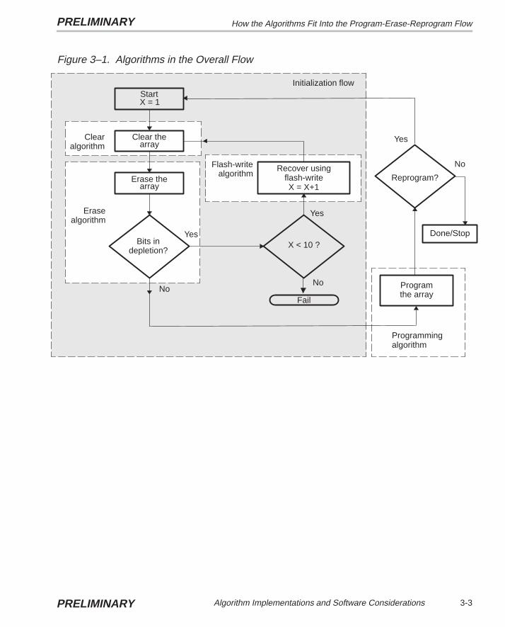
The programming algorithm and the clear algorithm are both implementationsof the program operation. The difference between the two is the data that iswritten: the programming algorithm programs the user data, while the clear al-gorithm uses all 0s. All of the algorithms can be viewed as portions of a singleflow diagram, as shown in Figure 3–1.
Note that in the algorithm flowcharts, the variable X represents the number ofattempts at depletion recovery using the flash-write algorithm. It has beenshown that if flash-write is not successful in depletion recovery after ten at-tempts, depletion recovery is not possible, and a device failure has occurred.Therefore, if ten flash-write attempts at depletion recovery are not successful,the algorithm returns a device failure error message.
How the Algorithms Fit Into the Program-Erase-Reprogram FlowPRELIMINARY
3-3Algorithm Implementations and Software ConsiderationsPRELIMINARY
Figure 3–1. Algorithms in the Overall Flow
Flash-writealgorithm
Erasealgorithm
Clearalgorithm
X = X+1flash-write
Recover using
Fail
Yes
No
X < 10 ?
arrayErase the
Clear thearray
No
Yes
Reprogram?
Bits indepletion?
X = 1Start
Programthe array
Initialization flow
Programmingalgorithm
No
Yes
Done/Stop

Programming (or Clear) Algorithm PRELIMINARY
3-4 PRELIMINARY
3.2 Programming (or Clear) Algorithm
The programming algorithm sequentially writes any number of addresses witha specified bit pattern.This algorithm is used to program application code ordata into the flash array. With a slight modification, the same algorithm per-forms the clear portion of the initialization flow (i.e., programs all bits to zero).In this role, the algorithm is called the clear algorithm. For the clear algorithm,the values programmed are always 0000h, while the values for applicationcode can be any combination of 1s and 0s. Figure 3–2 highlights the program-ming and clear algorithms’ place in the overall flow.
Figure 3–2. The Programming Algorithm in the Overall Flow
Flash-writealgorithm
Erasealgorithm
Clearalgorithm
X = X+1flash-write
Recover using
Fail
Yes
No
X < 10 ?
arrayErase the
Clear thearray
No
Yes
Reprogram?
Bits indepletion?
X = 1Start
Programthe array
Initialization flow
Programmingalgorithm
No
Yes
Done/Stop

Programming (or Clear) AlgorithmPRELIMINARY
3-5Algorithm Implementations and Software ConsiderationsPRELIMINARY
The main feature of the program/clear algorithm is the concept of program-ming an entire row of bits in a group. The ’F20x/F24x flash array is organizedin rows of 32 words. That is, addresses 0000h through 001Fh are physicallylocated on the same row of the flash memory array. The array is designed sothat there is a dependence between the charge levels on adjacent (even–odd)addresses during programming. Programming the bits of an odd address re-duces the charge margin of the programmed bits (the 0s) in the preceding ad-jacent (even) address within the row. Similarly, programming the bits of aneven address reduces the charge margin of the programmed bits in the nextadjacent (odd) address within the row. Because of this dependence, if eachaddress is programmed individually, the charge levels among programmedbits is not uniform. The programming algorithm improves the uniformity ofcharge levels on programmed bits by programming all of the words of a rowin a group. For example, the contents of address 0000h is compared with thedata to be programmed and one program pulse is applied if necessary. Thesame procedure is performed on addresses 0001h through 001Fh. The proce-dure repeats starting at address 0000h until no more program pulses are re-quired for any address in the row. The number of iterations of this loop equalsthe maximum number of program pulses required to program the bits in therow.
The flow for the programming algorithm is shown in Figure 3–3, and the as-sembly code is given in Appendix A.
An important consideration for programming the flash array is the CPU fre-quency range for the application. Because of the actual implementation of theflash memory circuitry, a 0 bit is most easily read at high frequency; pro-grammed bits have less margin when read at lower frequency. So, if the ap-plication requires a variable CPU clock rate, programming should be per-formed at the lowest frequency in the range. (A similar condition exists for theerase operation, which requires execution of the erase algorithm at the highestfrequency in the range. See section 3.3, page 3-10.)
Only the read portion of the program operation must be performed at the lowerfrequency, because the read is used to determine margin. The read operationcan be extended by sequentially executing multiple reads on the same loca-tion. Because the same address is selected the entire time and internal controlsignals are maintained between reads, the final read is equivalent to a slowread. For example, if the DSP core is executing the programming algorithm ata CLKOUT rate of 20 MHz (50 ns), sequentially reading a location three timesis equivalent to reading it once at 6.67 MHz (150 ns). This is important, be-cause it facilitates execution of the program and erase algorithms at the sameCLKOUT rate.

Programming (or Clear) Algorithm PRELIMINARY
3-6 PRELIMINARY
Figure 3–3. Programming or Clear Algorithm Flow
Same row
Device failureContinue
Currentaddress >
end address?
No
Yes
Row_done=
true?
No
Yes
No
Yes
Endof
row?
No
Yes
Pulsecount�=max†?
Apply programpulse;
row_done = false
Incrementaddress
New row
Verify con-tents
of currentaddress
Current address= row start address;
row_done = true
Save row startaddress
No
YesProgram
pulserequired?
Start
Steps 2–5 in Table 3–1
Step 6 in Table 3–1Steps 7–25in Table 3–1
† See the device data sheet for the timing parameter values.

Programming (or Clear) AlgorithmPRELIMINARY
3-7Algorithm Implementations and Software ConsiderationsPRELIMINARY
Another important consideration is the total amount of time required to do theprogramming. The number of programming pulses required to completely pro-gram a flash memory cell increases as ambient temperature increases and/orsupply voltage decreases. More programming pulses are required when theminimum supply voltage is used than when the nominal or maximum supplyvoltage is used. The number of program pulses required also increasesthroughout the life of the device, as more program-erase cycles are carriedout. The device data sheet specifies the maximum number of program pulsesunder all operating conditions; use this number when you calculate the maxi-mum amount of time required for programming.
The algorithm incorporates the steps for applying a program pulse (outlinedin Table 3–1) along with some other techniques to ensure margin. In general,not all flash bits require the same number of program pulses to reach the pro-grammed margin level. For this reason, the programming algorithm applies aseries of short program pulses until the memory location is programmed. How-ever, to understand how the series of program pulses works, you must first un-derstand how the algorithm applies a single program pulse. Table 3–1 outlinesthe steps involved in verifying programmed bits and applying a single pulse toeach of the upper and lower bytes of a single location. This process corre-sponds to the steps enclosed in the dashed box in the flowchart in Figure 3–3.
Table 3–1. Steps for Verifying Programmed Bits and Applying One Program or ClearPulse
Step Action Description
1 Power up the VCCP pin. Set the VCCP pin to VDD. If the VCCP pin for the flash module to be pro-grammed is not set to VDD, then the array will not be programmed.
2 Activate VER0 mode. Set the VER0 bit in SEG_CTR (load SEG_CTR with 0010h).
3 Delay for VER0 referencevoltage stabilization.
The CPU executes a delay loop for the td(VERIFY-SETUP†) time period.
4 Read flash array contents forverification.
The CPU reads the addressed location. The flash module must be inarray-access mode (see section 2.2, Accessing the Flash Module, page2-5).
5 Deactivate VER0 mode. Clear the VER0 bit in SEG_CTR (load SEG_CTR with 0000h).
6 Compare contents of flashlocation (16 bits) with de-sired data.
If the verification passes (i.e., if the data read in step 4 is equal to the de-sired data value), then no further program pulses are required. The flashword has been programmed with the desired data value. The programor clear function is completed and this algorithm is exited.
If the verification fails (i.e., if the data read in step 4 is not equal to thedesired data value), then proceed to step 7.
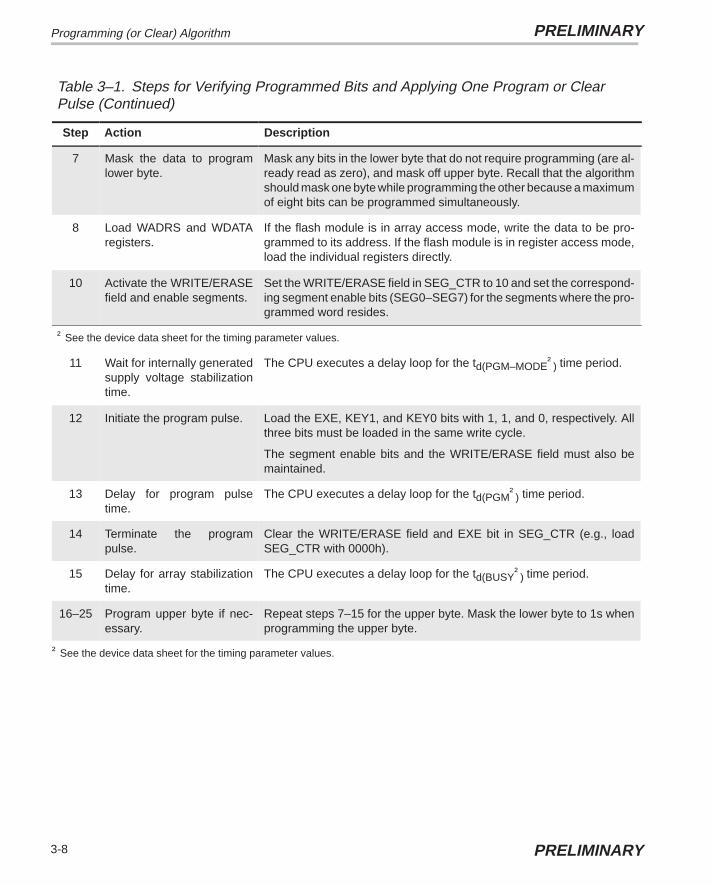
Programming (or Clear) Algorithm PRELIMINARY
3-8 PRELIMINARY
Table 3–1. Steps for Verifying Programmed Bits and Applying One Program or ClearPulse (Continued)
Step DescriptionAction
7 Mask the data to programlower byte.
Mask any bits in the lower byte that do not require programming (are al-ready read as zero), and mask off upper byte. Recall that the algorithmshould mask one byte while programming the other because a maximumof eight bits can be programmed simultaneously.
8 Load WADRS and WDATAregisters.
If the flash module is in array access mode, write the data to be pro-grammed to its address. If the flash module is in register access mode,load the individual registers directly.
10 Activate the WRITE/ERASEfield and enable segments.
Set the WRITE/ERASE field in SEG_CTR to 10 and set the correspond-ing segment enable bits (SEG0–SEG7) for the segments where the pro-grammed word resides.
† See the device data sheet for the timing parameter values.
11 Wait for internally generatedsupply voltage stabilizationtime.
The CPU executes a delay loop for the td(PGM–MODE†) time period.
12 Initiate the program pulse. Load the EXE, KEY1, and KEY0 bits with 1, 1, and 0, respectively. Allthree bits must be loaded in the same write cycle.
The segment enable bits and the WRITE/ERASE field must also bemaintained.
13 Delay for program pulsetime.
The CPU executes a delay loop for the td(PGM†) time period.
14 Terminate the programpulse.
Clear the WRITE/ERASE field and EXE bit in SEG_CTR (e.g., loadSEG_CTR with 0000h).
15 Delay for array stabilizationtime.
The CPU executes a delay loop for the td(BUSY†) time period.
16–25 Program upper byte if nec-essary.
Repeat steps 7–15 for the upper byte. Mask the lower byte to 1s whenprogramming the upper byte.
† See the device data sheet for the timing parameter values.

Programming (or Clear) AlgorithmPRELIMINARY
3-9Algorithm Implementations and Software ConsiderationsPRELIMINARY
Before each program pulse is applied, a read of the byte is performed to deter-mine which bits have reached the programmed level. Any bits that havereached the programmed level are masked (set to 1 in the WDATA register).This method of programming provides uniform charge levels among pro-grammed bits, whereas using a single, long program pulse could result insome bits having much more charge than others. The uniformity of charge lev-els among bits has the primary effect of reducing programming time and thesecondary effect of reducing the time for a subsequent erase operation. To as-sure that the bits are programmed with enough margin, the reads associatedwith programming use the VER0 read mode.

Erase Algorithm PRELIMINARY
3-10 PRELIMINARY
3.3 Erase Algorithm
The erase algorithm follows the clear algorithm in executing the entire initial-ization flow. Figure 3–4 highlights the erase algorithm’s place in the overallflow.
Figure 3–4. Erase Algorithm in the Overall Flow
Flash-writealgorithm
Erasealgorithm
Clearalgorithm
X = X+1flash-write
Recover using
Fail
Yes
No
X < 10 ?
arrayErase the
Clear thearray
No
Yes
Reprogram?
Bits indepletion?
X = 1Start
Programthe array
Initialization flow
Programmingalgorithm
No
Yes
Done/Stop
The erase algorithm consists of multiple iterations of a loop with one erasepulse applied in each iteration. Table 3–2 outlines the steps involved in apply-ing a single erase pulse.

Erase AlgorithmPRELIMINARY
3-11Algorithm Implementations and Software ConsiderationsPRELIMINARY
Table 3–2. Steps for Applying One Erase Pulse
Step Action Description
1 Power up the VCCP pin. Set VCCP pin to VDD. If the VCCP pin for the flash module to be erasedis not set to VDD, then the array will not be erased properly.
2 Load WDATA register withFFFFh.
This load overrides the erase protection mechanism.
3 Activate the erase mode andenable segments.
Set the WRITE/ERASE field to 01 and set SEG0–SEG7 bits in theSEG_CTR register. The flash module must be in register-accessmode (see section 2.2).
4 Wait for internally generatedsupply voltage stabilizationtime.
The CPU executes a delay loop for the td(ERASE-MODE†) time period.
5 Initiate the erase pulse. Load the EXE, KEY1, and KEY0 bits with 1, 1, and 0, respectively. Allthree bits must be loaded in the same write cycle.
The segment enable bits and the WRITE/ERASE field must also bemaintained.
6 Delay for erase pulse time. The CPU executes a delay loop for the td(ERASE†) time period.
7 Terminate the erase pulse. Clear the EXE bit and WRITE/ERASE field in the SEG_CTR register(load SEG_CTR with 0000h to clear all bits).
8 Delay for mode deselecttime.
CPU executes a delay loop for the td(BUSY†) time period.
† See the device data sheet for the timing parameter values.
At the beginning of each iteration, a read operation is performed on all the bitsin the array to determine if an erase pulse is required. Erasure is completewhen all array locations are read as FFFFh. To assure that the flash array iserased with enough margin, the reads associated with the erase use the VER1read mode. Additional margin can be gained during the erase operation if thereads are performed using address complementing. When the array is readwith address complementing, the following sequence is used for each addressread:
1) All of the bits of the address to be read are complemented.
2) The contents of the resulting address are read.
3) The value read at the complemented address is discarded.

Erase Algorithm PRELIMINARY
3-12 PRELIMINARY
4) The actual address is restored.
5) The contents of the restored address are read.
The advantage of this approach is that it forces the worst-case switching condi-tion on the flash addressing logic during the reads, thus improving the marginof the erase. Address complementing on the ’F20x/F24x can be accomplishedeasily by using the XOR instruction to complement the bits of the address.
An important consideration for erasing the flash array is the CPU frequencyrange for the application. Because of the actual implementation of the flashmemory circuitry, a logic 1 is most easily read at low frequency; erased bitshave less margin when read at higher frequency. Accordingly, if the applicationrequires a variable CPU clock rate, the erase should be performed at the high-est frequency in the range. (A similar condition exists for the programming op-eration, which requires execution of the programming algorithm at the lowestfrequency in the range. See section 3.2, page 3-4.)
Another important consideration is the total amount of time required to erasethe array. The number of erase pulses required to completely erase a flashmemory cell increases as ambient temperature increases or decreases rela-tive to the nominal temperature and as supply voltage decreases. More erasepulses are required when the ambient temperature is toward the extremes ofthe operating range. Also, more erase pulses are required when the minimumsupply voltage is used than when the nominal or maximum supply voltage isused. The number of erase pulses required also increases throughout the lifeof the device, as more program-erase cycles are carried out. The device datasheet specifies the maximum number of erase pulses under all operating con-ditions; use this number when you calculate the maximum amount of time re-quired for the erase algorithm.
The complete erase algorithm including depletion check is shown in the flow-chart in Figure 3–5.

Erase AlgorithmPRELIMINARY
3-13Algorithm Implementations and Software ConsiderationsPRELIMINARY
Figure 3–5. Erase Algorithm Flow
Program array
check
ÁÁ
Depletion
Yes
No
ÁÁAll
32 words= 0000h?
Read first32 words
Wait fortd(BUSY-INVERSE)
Set VER0 andVER1 bits inSEG_CTR
ÁÁ
Clear all bitsin SEG_CTR
Start(all words=0000h)
eraseVerify
No
Yes
No
Yes
Erasepulse count
≥ Max† ?
Device failure
Apply oneerase pulse
to flash array(see Table 3–2)
Allwords =FFFFh
?
Read all locationsusing addresscomplementing
Wait fortd(BUSY-VERIFY)
Set VER1bit in SEG_CTR
† See the device data sheet for the timing parameter values.
Depletionrecovery

Flash-Write Algorithm PRELIMINARY
3-14 PRELIMINARY
3.4 Flash-Write Algorithm
The flash-write operation recovers bits in depletion mode, which can becaused by over-erasure. The flash-write algorithm’s place in the overall flowis highlighted in Figure 3–6.
Figure 3–6. Flash-Write Algorithm in the Overall Flow
Flash-writealgorithm
Erasealgorithm
Clearalgorithm
X = X+1flash-write
Recover using
Fail
Yes
No
X < 10 ?
arrayErase the
Clear thearray
No
Yes
Reprogram?
Bits indepletion?
X = 1Start
Programthe array
Initialization flow
Programmingalgorithm
No
Yes
Done/Stop
A flash-write pulse is the time during the flash-write operation between the set-ting and the clearing of the EXE bit (bit 0 of SEG_CTR). Charge is added tothe bits of the flash memory array via the flash-write mechanism. The flash-write algorithm may require multiple flash-write pulses. The steps required toapply one flash-write pulse are outlined in Table 3–3.

Flash-Write AlgorithmPRELIMINARY
3-15Algorithm Implementations and Software ConsiderationsPRELIMINARY
Table 3–3. Steps for Applying One Flash-Write Pulse
Steps Action Description
1 Power up the VCCP pin. Set the VCCP pin to VDD. If the VCCP pin for the flash module to be re-covered is not set to VDD, then the flash-write operation will not be ef-fective.
2 Activate the flash-writemode and enable all seg-ments.
Set the WRITE/ERASE field to 10 and set SEG0–SEG7 in theSEG_CTR register. The flash module must be in register accessmode (see section 2.2).
3 Wait for the internally gener-ated supply voltage stabi-lization time.
The CPU executes a delay loop for the td(FLW-MODE†) time period.
4 Initiate the flash-write pulse. Load the EXE, KEY1, and KEY0 bits with 1, 1, and 0, respectively. Allthree bits must be loaded in the same write cycle.
The segment enable bits and WRITE/ERASE field must also be main-tained.
5 Delay for the flash-writepulse time.
The CPU executes a delay loop for the td(FLW†) time period.
6 Terminate the flash-writepulse.
Clear all bits in the SEG_CTR register (load SEG_CTR with 0000h).
7 Delay for mode deselecttime.
CPU executes a delay loop for the td(BUSY†) time period.
† See the device data sheet for the timing parameter values.
The flash-write algorithm consists of multiple iterations of a loop with one flash-write pulse applied in each iteration. At the beginning of each iteration, a deple-tion test is performed to determine if a flash-write pulse is required. Figure 3–7shows the flow of the flash-write algorithm.
The flash-write operation uses the inverse-erase read mode to detect bits thatare in depletion mode. For more information about the inverse-erase readmode, see section 2.4, Read Modes, on page 2-12.

Flash-Write Algorithm PRELIMINARY
3-16 PRELIMINARY
Figure 3–7. Flash-Write Algorithm Flow
Start
Depletioncheck
No
Yes
No
Yes
Flash-writepulse count
≥ Max† ?
Device failure
Apply one flash-writepulse to flash array
(see Table 3–3)
All 32words =0000h?
Read first 32 words
Wait fortd(RD-VERIFY)
Set VER0 and VER1bits in SEG_CTR
Go to clear
† See the device data sheet for the timing parameter values.
Flash-Write AlgorithmPRELIMINARY
3-17Algorithm Implementations and Software ConsiderationsPRELIMINARY
The CPU frequency range for the application is an important consideration forthe depletion test, as well as for the program and erase operations. Becauseof the actual implementation of the flash memory circuitry, a bit in depletionmode is most easily detected at low frequency. Accordingly, if the applicationrequires a variable CPU clock rate, the depletion test should be performed atthe lowest frequency in the range. Only the read portion of the depletion testmust be performed at the lower frequency, because it is the read that is usedto detect depletion. The effective duration of the read operation can be ex-tended by sequentially executing multiple reads on the same location. Be-cause the same address is selected the entire time and internal control signalsare maintained between reads, the final read is equivalent to a slow read. Forexample, if the DSP core is executing the programming algorithm at aCLKOUT rate of 20 MHz (50 ns), sequentially reading a location three timesis equivalent to reading it once at 6.67 MHz (150 ns). The erase and flash-writealgorithm implementations given in Appendix A use three reads to check fordepletion.

A-1
Appendix A
Assembly Source Listings andProgram Examples
The flash array is erased and programmed by code running on the DSP core.This code can originate from off-chip memory or can be loaded into on-chipRAM. The available flash programming tools for the ’F20x/F24x allow you toprogram the on-chip flash module without having knowledge or visibility of thealgorithms. One scheme uses the scan emulation feature of the ’F20x/F24x toload the algorithms onto the DSP and control execution, and another schemerelies on boot loader code preprogrammed into the flash memory at the facto-ry. You can find more information about these stand-alone flash programmingtools on the Texas Instruments web page at http://www.ti.com. This appendixexplains how to use the algorithm source files to program the flash module.You need this information to create new flash programming tools or to addsuch features as remote reprogrammability to a design.
Topic Page
A.1 Assembly Source for Algorithms A-2. . . . . . . . . . . . . . . . . . . . . . . . . . . . . . .
A.2 C-Callable Interface to Flash Algorithms A-27. . . . . . . . . . . . . . . . . . . . . . .
A.3 Sample Assembly Code to Erase and Reprogramthe TMS320F206 A-32. . . . . . . . . . . . . . . . . . . . . . . . . . . . . . . . . . . . . . . . . . . . .
A.4 Sample C Code to Erase and Reprogram the TMS320F206 A-37. . . . . .
A.5 Sample Assembly Code to Erase and Reprogramthe TMS320F240 A-40. . . . . . . . . . . . . . . . . . . . . . . . . . . . . . . . . . . . . . . . . . . . .
A.6 Using the Algorithms with C Code to Erase and Reprogram theTMS320F240 A-47. . . . . . . . . . . . . . . . . . . . . . . . . . . . . . . . . . . . . . . . . . . . . . . . .
Appendix A
PRELIMINARY
PRELIMINARY

Assembly Source for Algorithms PRELIMINARY
A-2 PRELIMINARY
A.1 Assembly Source for Algorithms
The algorithm source files implement the flows given in Chapter 3. Each algo-rithm is written as an assembly language subroutine, beginning with a label atan entry point and ending with a return instruction. The algorithms share a setof 16 relocatable variables for which pointers are defined in the header file,SVAR20.H.
The variables are defined at the beginning of B1 RAM, and an uninitialized sec-tion should be declared at link time to reserve this space. Also, the data pagepointer (DP) should be initialized to point to this space before a call is made toany of the algorithms.
In addition to these variables, each algorithm references parameters thatshould be declared globally in the calling code. These parameters are listed inthe introduction to each of the algorithm source files below.
The source files given are:
� SVAR20.H: header file that defines variables and constants� SCLR20.ASM: clear algorithm� SERA20.ASM: erase algorithm� SFLW20.ASM: flash-write algorithm� SPGM20.ASM: programming algorithm� SUTILS20.ASM: subroutines common to all four algorithms
The same algorithm files can be used for the TMS320F206 and theTMS320F240/1/3 devices. A conditional assembly variable is provided in theheader file, SVAR20.H, for assembling the algorithms for the correct device.For more details on this conditional assembly variable, see A.1.1.
A.1.1 Header File for Constants and Variables, SVAR20.H
This header file is included in each of the algorithm files using the .include di-rective. All of the constants used for flash programming are defined in this file.Also, the conditional assembly constant, F24x, is defined here to allow reuseof the algorithms for multiple device types. This constant should be modifiedto select the correct device when the algorithms are assembled. TheSVAR20.H header file can also be included in the calling code, to allow visibilityto the variable names.

Assembly Source for AlgorithmsPRELIMINARY
A-3Assembly Source Listings and Program ExamplesPRELIMINARY
**************************************************************** Variable declaration file *** *** TMS320F2XX Flash Utilities. *** Revision: 2.0, 9/10/97 *** Revision: 2.1, 1/31/98 *** *** Filename: svar20.asm *** ***Note: ***DLOOP is a delay loop variable used in flash algorithms. ***This is a function of CLKOUT1. If the F206 device runs at ***any CLKOUT1 speed other than 20 MHz, DLOOP value should be ***redefined per the equation explained below. Use of ***current DLOOP for flash programming at speeds other than ***20 MHz is not recommended. ****************************************************************
.mmregsBASE .set 0300h ;Base address for variables
;can be changed to relocate;variable space in RAM.
BASE_0 .set BASE+0 ;Scratch pad registers.BASE_1 .set BASE+1 ;BASE_2 .set BASE+2 ;BASE_3 .set BASE+3 ;BASE_4 .set BASE+4 ;BASE_5 .set BASE+5 ;BASE_6 .set BASE+6 ;SPAD1 .set BASE+7 ;SPAD2 .set BASE+8 ;FL_ADRS .set BASE+10 ;Flash load address.FL_DATA .set BASE+11 ;Flash load data.ERROR .set BASE+15 ;Error flag register.*Variables for ERASE and CLEARRPG_CNT .set BASE+12 ;Program pulse count.FL_ST .set BASE+13 ;Flash start addr/Seg Cntrl Reg.FL_END .set BASE+14 ;Flash end address.*
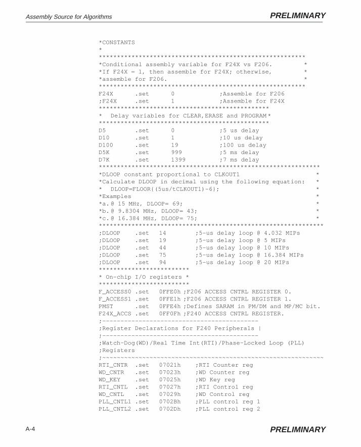
Assembly Source for Algorithms PRELIMINARY
A-4 PRELIMINARY
*CONSTANTS***********************************************************Conditional assembly variable for F24X vs F206. **If F24X = 1, then assemble for F24X; otherwise, **assemble for F206. **********************************************************F24X .set 0 ;Assemble for F206;F24X .set 1 ;Assemble for F24X************************************************ Delay variables for CLEAR,ERASE and PROGRAM ************************************************D5 .set 0 ;5 us delayD10 .set 1 ;10 us delayD100 .set 19 ;100 us delayD5K .set 999 ;5 ms delayD7K .set 1399 ;7 ms delay**************************************************************DLOOP constant proportional to CLKOUT1 **Calculate DLOOP in decimal using the following equation: ** DLOOP=FLOOR{(5us/tCLKOUT1)–6}; **Examples **a. @ 15 MHz, DLOOP= 69; **b. @ 9.8304 MHz, DLOOP= 43; **c. @ 16.384 MHz, DLOOP= 75; ***************************************************************;DLOOP .set 14 ;5–us delay loop @ 4.032 MIPs;DLOOP .set 19 ;5–us delay loop @ 5 MIPs;DLOOP .set 44 ;5–us delay loop @ 10 MIPs;DLOOP .set 75 ;5–us delay loop @ 16.384 MIPs;DLOOP .set 94 ;5–us delay loop @ 20 MIPs************************** On–chip I/O registers **************************F_ACCESS0 .set 0FFE0h ;F206 ACCESS CNTRL REGISTER 0.F_ACCESS1 .set 0FFE1h ;F206 ACCESS CNTRL REGISTER 1.PMST .set 0FFE4h ;Defines SARAM in PM/DM and MP/MC bit.F24X_ACCS .set 0FF0Fh ;F240 ACCESS CNTRL REGISTER.;–––––––––––––––––––––––––––––––––––––––––––;Register Declarations for F240 Peripherals |;–––––––––––––––––––––––––––––––––––––––––––;Watch–Dog(WD)/Real Time Int(RTI)/Phase–Locked Loop (PLL);Registers;~~~~~~~~~~~~~~~~~~~~~~~~~~~~~~~~~~~~~~~~~~~~~~~~~~~~~~~~~~~~~RTI_CNTR .set 07021h ;RTI Counter regWD_CNTR .set 07023h ;WD Counter regWD_KEY .set 07025h ;WD Key regRTI_CNTL .set 07027h ;RTI Control regWD_CNTL .set 07029h ;WD Control regPLL_CNTL1 .set 0702Bh ;PLL control reg 1PLL_CNTL2 .set 0702Dh ;PLL control reg 2
Assembly Source for AlgorithmsPRELIMINARY
A-5Assembly Source Listings and Program ExamplesPRELIMINARY
A.1.2 Clear Algorithm, SCLR20.ASM
This code is an implementation of the clear (programming) algorithm de-scribed in section 3.2 on page 3-4. Recall that the clear algorithm is identical tothe programming algorithm with the data forced to 0000h for all flash address-es.
Memory section: fl_clr
Entry point: GCLR
Parameters to be declared and initialized by the calling code are:
� PROTECT defines the values of bits 8–15 of SEG_CTR during the clearalgorithm.
� SEG_ST defines the start address of the flash array to be cleared.
� SEG_END defines the end address of the flash array to be cleared.
Return value: ERROR (@BASE+15); 0 = Pass, 1 = Fail
**************************************************************** CLEAR Subroutine *** *** TMS320F2XX Flash Utilities. *** Revision: 2.0, 9/10/97 *** Revision: 2.1, 1/31/98 *** *** Filename: sclr20.asm *** *** Called by: c2xx_bcx.asm or flash application programs. *** *** !!CAUTION – INITIALIZE DP BEFORE CALLING THIS ROUTINE!! *** *** Function: Clears one or more contiguous segments of *** array 0/1 as specified by the following *** variables. *** SEG_ST Segment start address *** SEG_END Segment end address *** PROTECT Sector protect enable *** ** The algorithm used is ”row-horizontal”, which means that ** an entire flash row (32 words) is programmed in parallel.** This method provides better uniformity of programming ** levels between adjacent bits than if each address were ** programmed independently. The algorithm also uses a ** 3-read check for VER0 margin (i.e.,the flash location is ** read three times and the first two values are discarded.)** This provides low–frequency read–back margin on *
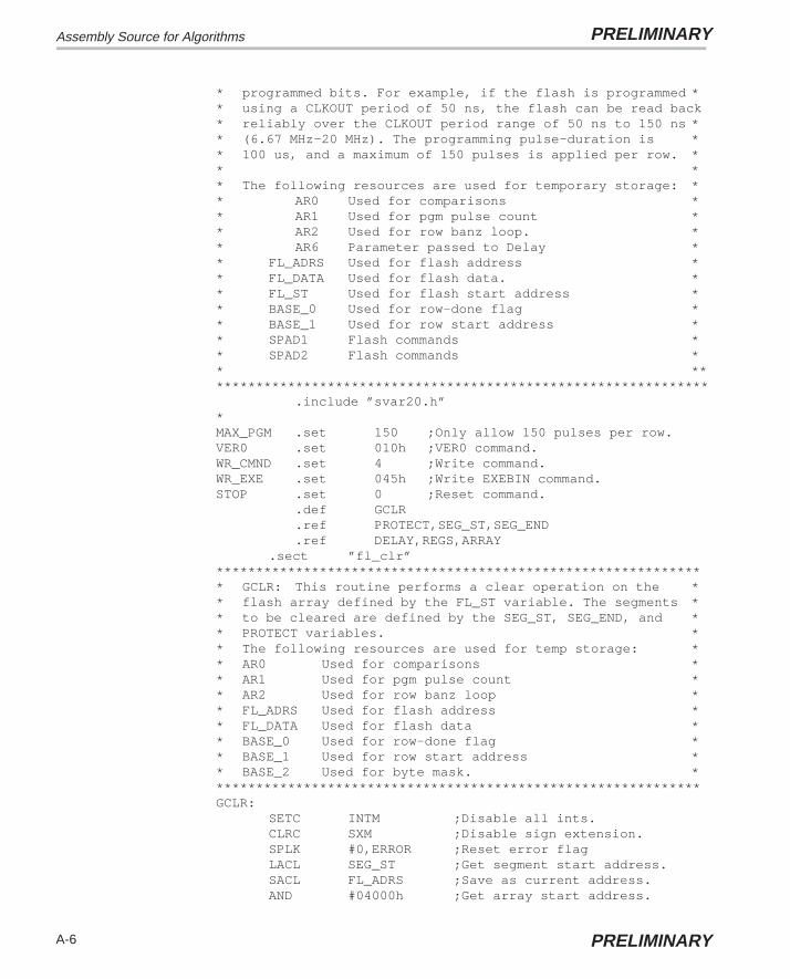
Assembly Source for Algorithms PRELIMINARY
A-6 PRELIMINARY
* programmed bits. For example, if the flash is programmed ** using a CLKOUT period of 50 ns, the flash can be read back* reliably over the CLKOUT period range of 50 ns to 150 ns ** (6.67 MHz–20 MHz). The programming pulse-duration is ** 100 us, and a maximum of 150 pulses is applied per row. ** ** The following resources are used for temporary storage: ** AR0 Used for comparisons ** AR1 Used for pgm pulse count ** AR2 Used for row banz loop. ** AR6 Parameter passed to Delay ** FL_ADRS Used for flash address ** FL_DATA Used for flash data. ** FL_ST Used for flash start address ** BASE_0 Used for row–done flag ** BASE_1 Used for row start address ** SPAD1 Flash commands ** SPAD2 Flash commands ** ****************************************************************
.include ”svar20.h”*MAX_PGM .set 150 ;Only allow 150 pulses per row.VER0 .set 010h ;VER0 command.WR_CMND .set 4 ;Write command.WR_EXE .set 045h ;Write EXEBIN command.STOP .set 0 ;Reset command.
.def GCLR
.ref PROTECT,SEG_ST,SEG_END
.ref DELAY,REGS,ARRAY.sect ”fl_clr”
************************************************************** GCLR: This routine performs a clear operation on the ** flash array defined by the FL_ST variable. The segments ** to be cleared are defined by the SEG_ST, SEG_END, and ** PROTECT variables. ** The following resources are used for temp storage: ** AR0 Used for comparisons ** AR1 Used for pgm pulse count ** AR2 Used for row banz loop ** FL_ADRS Used for flash address ** FL_DATA Used for flash data ** BASE_0 Used for row–done flag ** BASE_1 Used for row start address ** BASE_2 Used for byte mask. **************************************************************GCLR:
SETC INTM ;Disable all ints.CLRC SXM ;Disable sign extension.SPLK #0,ERROR ;Reset error flagLACL SEG_ST ;Get segment start address.SACL FL_ADRS ;Save as current address.AND #04000h ;Get array start address.
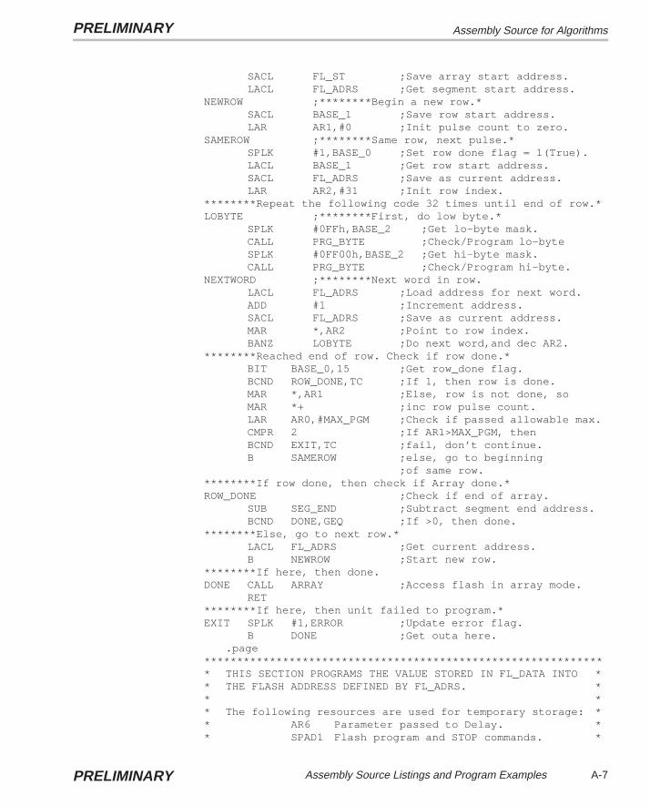
Assembly Source for AlgorithmsPRELIMINARY
A-7Assembly Source Listings and Program ExamplesPRELIMINARY
SACL FL_ST ;Save array start address.LACL FL_ADRS ;Get segment start address.
NEWROW ;********Begin a new row.*SACL BASE_1 ;Save row start address.LAR AR1,#0 ;Init pulse count to zero.
SAMEROW ;********Same row, next pulse.*SPLK #1,BASE_0 ;Set row done flag = 1(True).LACL BASE_1 ;Get row start address.SACL FL_ADRS ;Save as current address.LAR AR2,#31 ;Init row index.
********Repeat the following code 32 times until end of row.*LOBYTE ;********First, do low byte.*
SPLK #0FFh,BASE_2 ;Get lo–byte mask.CALL PRG_BYTE ;Check/Program lo–byteSPLK #0FF00h,BASE_2 ;Get hi–byte mask.CALL PRG_BYTE ;Check/Program hi–byte.
NEXTWORD ;********Next word in row.LACL FL_ADRS ;Load address for next word.ADD #1 ;Increment address.SACL FL_ADRS ;Save as current address.MAR *,AR2 ;Point to row index.BANZ LOBYTE ;Do next word,and dec AR2.
********Reached end of row. Check if row done.*BIT BASE_0,15 ;Get row_done flag.BCND ROW_DONE,TC ;If 1, then row is done.MAR *,AR1 ;Else, row is not done, soMAR *+ ;inc row pulse count.LAR AR0,#MAX_PGM ;Check if passed allowable max.CMPR 2 ;If AR1>MAX_PGM, thenBCND EXIT,TC ;fail, don’t continue.B SAMEROW ;else, go to beginning
;of same row.********If row done, then check if Array done.*ROW_DONE ;Check if end of array.
SUB SEG_END ;Subtract segment end address.BCND DONE,GEQ ;If >0, then done.
********Else, go to next row.*LACL FL_ADRS ;Get current address.B NEWROW ;Start new row.
********If here, then done.DONE CALL ARRAY ;Access flash in array mode.
RET********If here, then unit failed to program.*EXIT SPLK #1,ERROR ;Update error flag.
B DONE ;Get outa here..page
************************************************************** THIS SECTION PROGRAMS THE VALUE STORED IN FL_DATA INTO ** THE FLASH ADDRESS DEFINED BY FL_ADRS. ** ** The following resources are used for temporary storage: ** AR6 Parameter passed to Delay. ** SPAD1 Flash program and STOP commands. *

Assembly Source for Algorithms PRELIMINARY
A-8 PRELIMINARY
* SPAD2 Flash program + EXE command. **************************************************************EXE_PGM ;*
CALL ARRAY ;ACCESS ARRAY **LOAD WADRS AND WDATA **
LACL FL_ADRS ;ACC => PROGRAM ADRS *TBLW FL_DATA ;LOAD WADRS AND WDATA *
CALL REGS ;ACCESS FLASH REGS **SET UP WRITE COMMAND WORDS **
LACL PROTECT ;GET SEGMENT PROTECT MASK **OR #WR_CMND ;OR IN WRITE COMMAND **SACL SPAD1 ;SPAD1 = WRITE COMMAND **OR #WR_EXE ;OR IN EXEBIN COMMAND **SACL SPAD2 ;SPAD2 = WRITE EXE COMMAND **
* *LACL FL_ST ;ACC => 0 (FLASH0) *
* ACTIVATE WRITE BIT **TBLW SPAD1 ;EXECUTE COMMAND **LAR AR6,#D10 ;SET DELAY **
CALL DELAY,*,AR6 ;WAIT *** SET EXEBIN BIT **
TBLW SPAD2 ;EXECUTE COMMAND **LAR AR6,#D100 ;SET DELAY **
CALL DELAY,*,AR6 ;WAIT *** STOP WRITE OPERATION *
SPLK #0,SPAD1 ;SHUTDOWN WRITE OPERATION *TBLW SPAD1 ;EXECUTE COMMAND *LAR AR6,#D10 ;SET DELAY *
CALL DELAY,*,AR6 ;WAIT ** *
RET ;RETURN TO CALLING SEQUENCE*************************************************************
.page************************************************************* ACTIVATE VER0 ON FLASH READS ** LOADS FLASH WORD AT ADDR FL_ADRS TO FL_DATA. ** Uses SPAD1 for temporary storage of flash commands. *************************************************************SET_RD_VER0 ;*
CALL REGS ;ACCESS FLASH REGISTERS *LACL FL_ST ;ACC => FLASH *SPLK #VER0,SPAD1 ;ACTIVATE VER0 *TBLW SPAD1 ;EXECUTE COMMAND*LAR AR6,#D10 ;SET DELAY *CALL DELAY,*,AR6 ;WAIT *CALL ARRAY ;ACCESS FLASH ARRAY *LACL FL_ADRS ;POINT TO ADRS *TBLR FL_DATA ;GET FLASH WORD 1x read *TBLR FL_DATA ;2x read *TBLR FL_DATA ;3x read *CALL REGS ;ACCESS FLASH REGISTERS *LACL FL_ST ;ACC => FLASH *SPLK #STOP,SPAD1 ;DEACTIVATE VER0 *

Assembly Source for AlgorithmsPRELIMINARY
A-9Assembly Source Listings and Program ExamplesPRELIMINARY
TBLW SPAD1 ;EXECUTE COMMAND *LAR AR6,#D10 ;SET DELAY *CALL DELAY,*,AR6 ;WAIT *CALL ARRAY ;ACCESS FLASH ARRAY *RET ;RETURN TO CALLING SEQUENCE*
*************************************************************************************************************** PRG_BYTE: Programs hi or lo byte depending on ** byte mask (BASE_2). **************************************************PRG_BYTE:
CALL SET_RD_VER0 ;Read word at VER0 level.LACL BASE_2 ;Get lo/hi byte mask.AND FL_DATA ;Xor with read–back value.BCND PB_DONE,EQ ;If zero, then done.XOR #0FFFFh ;else, mask off good bits.SACL FL_DATA ;New data.CALL EXE_PGM ;PGM Pulse.SPLK #0,BASE_0 ;Set row done flag = 0(False).
PB_DONE RET************************************************
.end
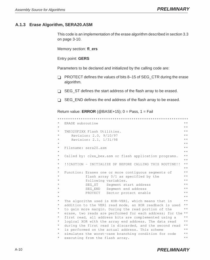
Assembly Source for Algorithms PRELIMINARY
A-10 PRELIMINARY
A.1.3 Erase Algorithm, SERA20.ASM
This code is an implementation of the erase algorithm described in section 3.3on page 3-10.
Memory section: fl_ers
Entry point: GERS
Parameters to be declared and initialized by the calling code are:
� PROTECT defines the values of bits 8–15 of SEG_CTR during the erasealgorithm.
� SEG_ST defines the start address of the flash array to be erased.
� SEG_END defines the end address of the flash array to be erased.
Return value: ERROR (@BASE+15); 0 = Pass, 1 = Fail
*************************************************************** ERASE subroutine *** *** TMS320F2XX Flash Utilities. *** Revision: 2.0, 9/10/97 *** Revision: 2.1, 1/31/98 *** *** Filename: sera20.asm *** *** Called by: c2xx_bex.asm or flash application programs. *** *** !!CAUTION – INITIALIZE DP BEFORE CALLING THIS ROUTINE!! *** *** Function: Erases one or more contiguous segments of *** flash array 0/1 as specified by the *** following variables. *** SEG_ST Segment start address *** SEG_END Segment end address *** PROTECT Sector protect enable *** *** The algorithm used is XOR–VER1, which means that in *** addition to the VER1 read mode, an XOR readback is used *** to gain more margin. During the read portion of the *** erase, two reads are performed for each address; for the *** first read, all address bits are complemented using a *** logical XOR with the array end address. The data read *** during the first read is discarded, and the second read *** is performed on the actual address. This scheme *** simulates the worst–case branching condition for code *** executing from the flash array. **
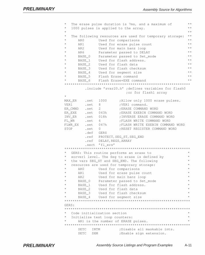
Assembly Source for AlgorithmsPRELIMINARY
A-11Assembly Source Listings and Program ExamplesPRELIMINARY
* The erase pulse duration is 7ms, and a maximum of *** 1000 pulses is applied to the array. *** *** The following resources are used for temporary storage: *** AR0 Used for comparisons *** AR1 Used for erase pulse count *** AR2 Used for main banz loop *** AR6 Parameter passed to DELAY *** BASE_0 Parameter passed to Set_mode *** BASE_1 Used for flash address. *** BASE_2 Used for flash data *** BASE_3 Used for flash checksum *** BASE_4 Used for segment size *** BASE_5 Flash Erase command *** BASE_6 Flash Erase+EXE command ***************************************************************
.include ”svar20.h” ;defines variables for flash0;or for flash1 array
*MAX_ER .set 1000 ;Allow only 1000 erase pulses.VER1 .set 8 ;VER1 command.ER_CMND .set 2 ;ERASE COMMAND WORDER_EXE .set 043h ;ERASE EXEBIN COMMAND WORDINV_ER .set 018h ;INVERSE ERASE COMMAND WORDFL_WR .set 6 ;FLASH WRITE COMMAND WORDFLWR_EX .set 047h ;FLASH WRITE EXEBIN COMMAND WORDSTOP .set 0 ;RESET REGISTER COMMAND WORD
.def GERS
.ref PROTECT,SEG_ST,SEG_END
.ref DELAY,REGS,ARRAY
.sect ”fl_ers”************************************************************** GERS: This routine performs an erase to ** xorver1 level. The Seg to erase is defined by ** the vars SEG_ST and SEG_END. The following ** resources are used for temporary storage: ** AR0 Used for comparisons ** AR1 Used for erase pulse count ** AR2 Used for main banz loop ** BASE_0 Parameter passed to Set_mode ** BASE_1 Used for flash address. ** BASE_2 Used for flash data ** BASE_3 Used for flash checksum ** BASE_4 Used for segment size **************************************************************GERS:************************************************************** Code initialization section ** Initialize test loop counters: ** AR1 is the number of ERASE pulses. **************************************************************
SETC INTM ;Disable all maskable ints.SETC SXM ;Enable sign extension.

Assembly Source for Algorithms PRELIMINARY
A-12 PRELIMINARY
CLRC OVM ;Disable overflow mode.LACL SEG_ST ;Get segment start address.AND #04000h ;Get array start address.SACL FL_ST ;Save array start address.OR #03FFFh ;Get array end address.SACL FL_END ;Save array end address.SPLK #0,ERROR ;Reset error flagLAR AR1,#0 ;Set erase count to 0.SPLK #STOP, BASE_0 ;Stop command.CALL SET_MODE ;Disable any flash cmds.
XOR_ERASE** Compute checksum for flash, using address complementing.**
LACC SEG_ENDSUB SEG_STSAC BASE_4 ;Segment length–1.LAR AR2,BASE_4 ;load n–1 to loop n times.ADD #1SACL BASE_4 ;Segment length.SPLK #VER1,BASE_0 ;VER1 command.CALL SET_MODE ;Set VER1 mode.MAR *,AR2BLDD #SEG_ST,BASE_1 ;Segment start address.SPLK #0,BASE_3 ;Clear checksum.
RD1_LOOP ;For I = SEG_ST to SEG_END.LACC BASE_1 ;ACC => CURRENT ADDR.XOR FL_END ;XOR addr with flash end addr.TBLR BASE_2 ;Dummy Read.LACC BASE_1 ;Get actual addr again.TBLR BASE_2 ;True Read.ADD #1 ;Increment flash addr.SACL BASE_1 ;Store for next read.LACC BASE_3 ;Get old check sum.ADD BASE_2 ;ACC=>ACC+FL_DATA.SACL BASE_3 ;Save new check sum.BANZ RD1_LOOP,*–ADD BASE_4 ;Should make ACC = 0 for
;erased array.BCND XOR_ERFIN,EQ ;If BASE_3 = 0, finished.
***** If not erased, apply an erase pulse.CALL ERASE_A ;Else, pulse it again.MAR *,AR1 ;ARP–>AR1 (Erase pulse count)MAR *+ ;Increment Erase count.LAR AR0,#MAX_ERCMPR2 ;If AR1>MAX_ER thenBCND EXIT,TC ;fail, don’t continue erasing.B XOR_ERASE ;Else, check again.
***** If here, then erase passed; now check for depletion.XOR_ERFIN
SPLK #STOP, BASE_0 ;Stop command.CALL SET_MODE ;Disable any flash cmds.CALL INV_ERASE ;Check for depletion.
DONE RET ;Return to calling code.

Assembly Source for AlgorithmsPRELIMINARY
A-13Assembly Source Listings and Program ExamplesPRELIMINARY
***** If here, then an error has occurred.EXIT SPLK #1,ERROR ;Update error flag
SPLK #STOP,BASE_0 ;Stop command.CALL SET_MODE ;Disable any flash cmds.B DONE ;Get outa here.
************************************************************.page
*************************************************** SET_MODE: This routine sets the flash in the ** mode specified by the contents of BASE_0. This ** can be used for VER0,VER1,INVERASE, or STOP. ** AR6: Parameter passed to DELAY. ***************************************************SET_MODE
CALL REGS ;ACCESS FLASH REGSLACL FL_ST ;ACC => SEG_CTR.TBLW BASE_0 ;Activate MODE.LAR AR6,#D10 ;SET DELAYCALL DELAY,*,AR6 ;WAIT *CALL ARRAY ;ACCESS FLASH ARRAY *RET
************************************************* INV_ERASE: This routine is used to check for ** depletion in the flash array. ** AR2 Used for main banz loop ** BASE_0 Parameter passed to Set_mode ** BASE_1 Used for flash address ** BASE_2 Used for flash data *************************************************INV_ERASE
SPLK #INV_ER,BASE_0CALL SET_MODE ;Set inverse–erase mode.BLDD #FL_ST,BASE_1 ;Array start address.LAR AR2,#31 ;Loop count.MAR *,AR2
NEXT_IVERSLACL BASE_1 ;Get address.TBLR BASE_2 ;Dummy read.TBLR BASE_2 ;Read data.ADD #1 ;Increment address.SACL BASE_1 ;Save address.ZACADD BASE_2 ;Add data.BCND EXIT,NEQ ;If ACC<>0, then fail.
*Else continue, until until done with row.BANZ NEXT_IVERS ;Loop 32 times.SPLK #STOP,BASE_0 ;Stop command.CALL SET_MODE ;Disable any flash cmds.RET ;If here then test passed..page
************************************************************** ERASE_A: This subroutine applies one erase pulse to the ** flash array. *
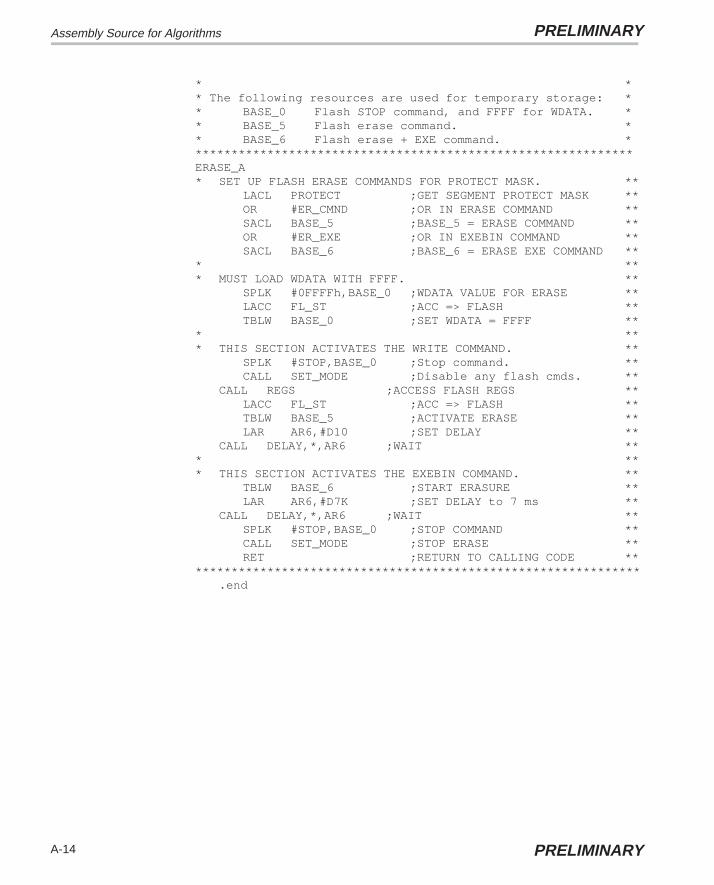
Assembly Source for Algorithms PRELIMINARY
A-14 PRELIMINARY
* ** The following resources are used for temporary storage: ** BASE_0 Flash STOP command, and FFFF for WDATA. ** BASE_5 Flash erase command. ** BASE_6 Flash erase + EXE command. **************************************************************ERASE_A* SET UP FLASH ERASE COMMANDS FOR PROTECT MASK. **
LACL PROTECT ;GET SEGMENT PROTECT MASK **OR #ER_CMND ;OR IN ERASE COMMAND **SACL BASE_5 ;BASE_5 = ERASE COMMAND **OR #ER_EXE ;OR IN EXEBIN COMMAND **SACL BASE_6 ;BASE_6 = ERASE EXE COMMAND **
* *** MUST LOAD WDATA WITH FFFF. **
SPLK #0FFFFh,BASE_0 ;WDATA VALUE FOR ERASE **LACC FL_ST ;ACC => FLASH **TBLW BASE_0 ;SET WDATA = FFFF **
* *** THIS SECTION ACTIVATES THE WRITE COMMAND. **
SPLK #STOP,BASE_0 ;Stop command. **CALL SET_MODE ;Disable any flash cmds. **
CALL REGS ;ACCESS FLASH REGS **LACC FL_ST ;ACC => FLASH **TBLW BASE_5 ;ACTIVATE ERASE **LAR AR6,#D10 ;SET DELAY **
CALL DELAY,*,AR6 ;WAIT *** *** THIS SECTION ACTIVATES THE EXEBIN COMMAND. **
TBLW BASE_6 ;START ERASURE **LAR AR6,#D7K ;SET DELAY to 7 ms **
CALL DELAY,*,AR6 ;WAIT **SPLK #STOP,BASE_0 ;STOP COMMAND **CALL SET_MODE ;STOP ERASE **RET ;RETURN TO CALLING CODE **
**************************************************************.end

Assembly Source for AlgorithmsPRELIMINARY
A-15Assembly Source Listings and Program ExamplesPRELIMINARY
A.1.4 Flash-Write Algorithm, SFLW20.ASM
This code is an implementation of the flash-write algorithm described in sec-tion 3.4 on page 3-14.
Memory section: fl_wrt
Entry point: FLWS
Parameters to be declared and initialized by the calling code are:
� PROTECT defines the values of bits 8–15 of SEG_CTR during the flash-write algorithm.
� SEG_ST defines the start address of the flash array to be recovered.
� SEG_END defines the end address of the flash array to be recovered.
Return value: ERROR (@BASE+15) 0=Pass, 1=Fail
**************************************************************** FLASH–WRITE subroutine *** *** TMS320F2XX Flash Utilities. *** Revision: 2.0, 9/10/97 *** Revision: 2.1, 1/31/98 *** *** Filename: sflw20.asm *** *** Called by : c2xx_bfx.asm or flash application programs. *** *** !!CAUTION – INITIALIZE DP BEFORE CALLING THIS ROUTINE!! *** *** Function: Performs flash writes on flash array 0/1 as *** specified by the following vars: *** SEG_ST Array segment start address *** PROTECT Sector protect enable *** ** The flash–write pulse duration used is 14 ms, and a ** maximum of 10000 pulses is applied until the device ** passes the depletion test. ** ** The following resources are used for temp storage: ** AR0 Used for comparison ** AR1 Flash–Write Pulse Count ** AR2 Used for main BANZ loop ** AR6 Parameter passed to DELAY ** BASE_0 Parameter passed to SET_MODE ** BASE_1 Used for flash address ** BASE_2 Used for flash data *
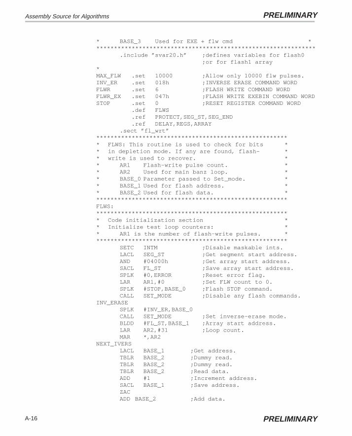
Assembly Source for Algorithms PRELIMINARY
A-16 PRELIMINARY
* BASE_3 Used for EXE + flw cmd ***************************************************************
.include ”svar20.h” ;defines variables for flash0;or for flash1 array
*MAX_FLW .set 10000 ;Allow only 10000 flw pulses.INV_ER .set 018h ;INVERSE ERASE COMMAND WORDFLWR .set 6 ;FLASH WRITE COMMAND WORDFLWR_EX .set 047h ;FLASH WRITE EXEBIN COMMAND WORDSTOP .set 0 ;RESET REGISTER COMMAND WORD
.def FLWS
.ref PROTECT,SEG_ST,SEG_END
.ref DELAY,REGS,ARRAY.sect ”fl_wrt”
******************************************************* FLWS: This routine is used to check for bits ** in depletion mode. If any are found, flash– ** write is used to recover. ** AR1 Flash–write pulse count. ** AR2 Used for main banz loop. ** BASE_0 Parameter passed to Set_mode. ** BASE_1 Used for flash address. ** BASE_2 Used for flash data. *******************************************************FLWS:******************************************************* Code initialization section ** Initialize test loop counters: ** AR1 is the number of flash–write pulses. *******************************************************
SETC INTM ;Disable maskable ints.LACL SEG_ST ;Get segment start address.AND #04000h ;Get array start address.SACL FL_ST ;Save array start address.SPLK #0,ERROR ;Reset error flag.LAR AR1,#0 ;Set FLW count to 0.SPLK #STOP,BASE_0 ;Flash STOP command.CALL SET_MODE ;Disable any flash commands.
INV_ERASESPLK #INV_ER,BASE_0CALL SET_MODE ;Set inverse–erase mode.BLDD #FL_ST,BASE_1 ;Array start address.LAR AR2,#31 ;Loop count.MAR *,AR2
NEXT_IVERSLACL BASE_1 ;Get address.TBLR BASE_2 ;Dummy read.TBLR BASE_2 ;Dummy read.TBLR BASE_2 ;Read data.ADD #1 ;Increment address.SACL BASE_1 ;Save address.ZACADD BASE_2 ;Add data.

Assembly Source for AlgorithmsPRELIMINARY
A-17Assembly Source Listings and Program ExamplesPRELIMINARY
BCND FL_WRITE, NEQ ;If ACC<>0, then flwrite.*Else, continue until until done with row.
BANZ NEXT_IVERS ;Loop 32 times.SPLK #STOP,BASE_0 ;Flash STOP command.CALL SET_MODE ;Disable flash commands.
;If here then test passed.DONE RET ;Return to calling code.* If here, then an error has occurred.EXIT SPLK #1,ERROR ;Update error flag
SPLK #STOP,BASE_0 ;Flash STOP command.CALL SET_MODE ;Disable flash commands.CALL ARRAY ;ACCESS FLASH ARRAYB DONE ;Get outa here..page
**************************************************** FL_WRITE: This routine performs a fl_write on ** the flash until a maximum is reached. The ** array is defined by the variable FL_ST ** and the segment(s) is defined by the PROTECT ** mask. The following resources are used for ** temporary storage: ** AR0 Used for comparison ** AR1 Used for pulse count (Global) ** AR6 Parameter passed to DELAY ** BASE_0 Parameter passed to SET_MODE ** BASE_2 Used for flw cmd ** BASE_3 Used for EXE + flw cmd ****************************************************FL_WRITE
SPLK #STOP,BASE_0 ;Flash STOP command.CALL SET_MODE ;Disable flash commands.LACL PROTECT ;Get sector_prot mask.OR #FLWR ;Or in fl_write cmd.SACL BASE_2 ;BASE_2 = fl_write cmd.OR #FLWR_EX ;Or in EXE + fl_write cmd.SACL BASE_3 ;BASE_3 = EXE + fl_write cmd.
*Set the flash–write command.CALL REGS ;Access flash regs.LACC FL_ST ;ACC => SEG_CTL.TBLW BASE_2 ;Initiate fl_write.LAR AR6,#D10 ;Set delay.CALL DELAY,*,AR6 ;Wait,10US flw stabilization time.
*Set the EXE bit (start flash–write pulse).TBLW BASE_3 ;Start flw pulse.LAR AR6,#D7K ;Set delay to 7 ms.CALL DELAY,*,AR6 ;WAIT,7 ms.LAR AR6,#D7K ;Set delay to 7 ms.CALL DELAY,*,AR6 ;WAIT 7 ms.
*A 14–mS flash write pulse has been applied.SPLK #STOP,BASE_0 ;Flash STOP command.CALL SET_MODE ;Disable flash commands.MAR *,AR1MAR *+ ;Increment flw count.
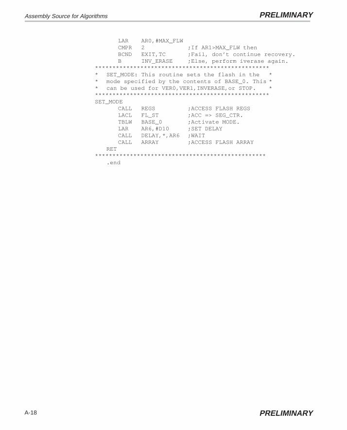
Assembly Source for Algorithms PRELIMINARY
A-18 PRELIMINARY
LAR AR0,#MAX_FLWCMPR 2 ;If AR1>MAX_FLW thenBCND EXIT,TC ;Fail, don’t continue recovery.B INV_ERASE ;Else, perform iverase again.
*************************************************** SET_MODE: This routine sets the flash in the ** mode specified by the contents of BASE_0. This ** can be used for VER0,VER1,INVERASE,or STOP. ***************************************************SET_MODE
CALL REGS ;ACCESS FLASH REGSLACL FL_ST ;ACC => SEG_CTR.TBLW BASE_0 ;Activate MODE.LAR AR6,#D10 ;SET DELAYCALL DELAY,*,AR6 ;WAITCALL ARRAY ;ACCESS FLASH ARRAY
RET*************************************************
.end

Assembly Source for AlgorithmsPRELIMINARY
A-19Assembly Source Listings and Program ExamplesPRELIMINARY
A.1.5 Programming Algorithm, SPGM20.ASM
This code is an implementation of the program algorithm described in section3.2 on page 3-4.
Memory section: fl_prg
Entry point: GPGMJ
Parameters to be declared and initialized by the calling code are:
� PRG_bufaddr defines the destination start address.
� PRG_length defines the source buffer length.
� PRG_paddr defines the source buffer start address (data space).
� PROTECT defines the values of bits 8–15 of SEG_CTR during the pro-gramming algorithm.
Return value: ERROR (@BASE+15); 0 = Pass, 1 = Fail
**************************************************************** PROGRAM Subroutine *** *** TMS320F2XX Flash Utilities. *** Revision: 2.0, 9/10/97 *** Revision: 2.0b, 12/5/97 *** Revision: 2.1, 1/31/98 *** *** Filename: spgm20.asm *** *** Called by: c2xx_bpx.asm or flash application programs. *** *** !!CAUTION – INITIALIZE DP BEFORE CALLING THIS ROUTINE!! *** *** Function: This routine programs all or part of the *** flash as specified by the variables: *** PRG_paddr Destination start address ** PRG_length Source buffer length ** PRG_bufaddr Source buffer start address ** ** The algorithm used is ”row–horizontal”, which means that ** an entire flash row (32 words) is programmed in parallel.** This method provides better uniformity of programming ** levels between adjacent bits than if each address were ** programmed independently. The algorithm also uses a ** 3–read check for VER0 margin (i.e., the flash location is** read three times and the first two values are discarded.)** This provides low–freq read–back margin on programmed *

Assembly Source for Algorithms PRELIMINARY
A-20 PRELIMINARY
* bits. For example, if the flash is programmed using a ** CLKOUT period of 50 ns, the flash can be reliably read ** back over the CLKOUT period range of 50 ns to 150 ns ** (6.67MHz–20 MHz). The programming pulse duration is ** 100 us, and a maximum of 150 pulses is applied per row. ** ** The following variables are used for temp storage: ** AR0 Used for comparisons ** AR1 Used for pgm pulse count ** AR2 Used for row banz loop ** AR3 Used for buffer addr index ** AR4 Used for flash address. ** AR6 Parameter passed to Delay ** SPAD1 Flash program and STOP commands ** SPAD2 Flash program + EXE command ** FL_ADRS Used for flash address ** FL_DATA Used for flash data ** BASE_0 Used for row–done flag ** BASE_1 Used for row start address ** BASE_2 Used for row length–1 ** BASE_3 Used for buffer/row start addr ** BASE_4 Used for destination end addr ** BASE_5 Used for byte mask **************************************************************
.include ”svar20.h”*MAX_PGM .set 150 ;Allow only 150 pulses per row.VER0 .set 010h ;VER0 command.WR_CMND .set 4 ;Write command.WR_EXE .set 045h ;Write EXEBIN command.STOP .set 0 ;Reset command.
.def GPGMJ
.ref PRG_bufaddr,PRG_length,PRG_paddr
.ref PROTECT,DELAY,REGS,ARRAY
.sect ”fl_prg”********************************************************** GPGMJ: This routine programs all or part of ** the flash as specified by the variables: ** PRG_paddr Destination start address ** PRG_length Source buffer length ** PRG_bufaddr Buffer start address ** ** The following variables are used for temp ** storage: ** AR0 Used for comparisons ** AR1 Used for pgm pulse count ** AR2 Used for row banz loop ** AR3 Used for buffer addr index ** FL_ADRS Used for flash address ** FL_DATA Used for flash data ** BASE_0 Used for row–done flag ** BASE_1 Used for row start address ** BASE_2 Used for row length–1 *

Assembly Source for AlgorithmsPRELIMINARY
A-21Assembly Source Listings and Program ExamplesPRELIMINARY
* BASE_3 Used for buffer/row start addr ** BASE_4 Used for destination end addr ** BASE_5 Used for byte mask *******************************************************GPGMJ: SPLK #0,IMR ;MASK ALL INTERRUPTS
SETC INTM ;GLOBALLY MASK ALL INTERRUPTSSPLK #0,ERROR ;Initialize error flag (no error).LACL PRG_paddr ;Get destination start address.SACL FL_ADRS ;Save as current address.ADD PRG_length ;Determine destination end addr.SUB #1 ;SACL BASE_4 ;Save destination end addr.LACL PRG_paddr ;Get destination start addr.LAR AR3,PRG_bufaddr ;Get buffer start address.
********Begin a new row.*NEWROW
SACL BASE_1 ;Save row start address.SAR AR3,BASE_3 ;Save buffer/row start address.LAR AR1,#0 ;Init pulse count to zero.SPLK #31,BASE_2 ;Init row length–1 to 31.AND #001Fh ;Is start addr on row boundary?CC ADJ_ROW,NEQ ;If not then adjust row length.LACL BASE_1 ;Get row start address.OR #001Fh ;Get row end address.SUB BASE_4 ;Is end address on row boundary?CC ADJ_ROW,GT ;If not then adjust row length.
********Same row, next pulse.*SAMEROW SPLK #1,BASE_0 ;Set row done flag = 1(True).
LACL BASE_1 ;Get row start address.SACL FL_ADRS ;Save as current address.LAR AR3,BASE_3 ;Get buffer/row start addr. LAR AR2,BASE_2 ;Init row index.
** Repeat the following code 32 times or until end of row.*LOBYTE ;********First, do low byte.*
CALL SET_MODULE,AR4 ;Determine which flash module.SPLK #0FFh,BASE_5 ;Set lo–byte mask.CALL PRG_BYTE ;Check/Program lo–byte.SPLK #0FF00h,BASE_5 ;Set hi–byte mask.
CALL PRG_BYTE ;Check/Program hi–byte.NEXTWORD ;********Next word in row.
LACL FL_ADRS ;Load address for next word.ADD #1 ;Increment address.SACL FL_ADRS ;Save as current address.MAR *,AR3 ;ARP –> buffer addr index.MAR *+,AR2 ;Inc, and ARP –> row index.BANZ LOBYTE ;Do next word,and dec AR2.
** Reached end of row. Check if row done. *BIT BASE_0,15 ;Get row_done flag.BCND ROW_DONE,TC ;If 1 then row is done.MAR *,AR1 ;Else, row is not done, soMAR *+ ;inc row pulse count.LAR AR0,#MAX_PGM ;Check if passed allowable max.CMPR 2 ;If AR1>MAX_PGM then

Assembly Source for Algorithms PRELIMINARY
A-22 PRELIMINARY
BCND EXIT,TC ;fail, don’t continue.B SAMEROW ;else, go to beginning
;of same row.** If row done, then check if Array done. *ROW_DONE
LACL FL_ADRS ;Check if end of array.SUB BASE_4 ;Subtract end addr.BCND DONE, GT ;If >0 then done.
** Else, go to next row. *LACL FL_ADRSB NEWROW ;Start new row.
** If here, then done.DONE
CALL ARRAY ;Access flash in array mode.RET ;Return to calling program.
** If here, then unit failed to program. *EXIT SPLK #1,ERROR ;Update error flag (error).
B DONE ;Get outa here.************************************************
.page************************************************* ADJ_ROW: This routine is used to adjust the ** row length, if the start or end address of ** code being programmed does not fall on a row ** boundary. The row length is passed in the ** BASE_2 variable, and the adjustment value to ** be subtracted is passed in the accumulator. ************************************************ADJ_ROW
NEG ;Take twos complement.ADD BASE_2 ;Add row length.SACL BASE_2 ;Save new row length.RET
************************************************** SET_MODULE: This routine is used to point to ** the appropriate flash array control register ** This is only important for ’F2XX devices with ** multiple flash modules like the 320F206. The ** variable FL_ST is returned with the correct ** register address. ** The following resources are used ** temporarily: ** AR0 Used for comparisons ** AR4 Used for flash address ****************************************************SET_MODULE
LAR AR4,FL_ADRS ;AR4 = current address.SPLK #0,FL_ST ;FL_ST = FLASH0 CTRL REGSLAR AR0,#4000H ;AR0 = compare value.CMPR 1 ;If AR4 < AR0 then
;FL_ADRS < 4000H; SET TCBCND FL0,TC ;Address is in FL0.
* ;Else address is in FL1.

Assembly Source for AlgorithmsPRELIMINARY
A-23Assembly Source Listings and Program ExamplesPRELIMINARY
SPLK #04000h,FL_ST ;FL_ST = FLASH1 CTRL REGSFL0 RET*************************************************************
.page************************************************************** THIS SECTION PROGRAMS THE VALUE STORED IN FL_DATA INTO ** THE FLASH ADDRESS DEFINED BY FL_ADRS. ** ** The following resources are used for temporary storage: ** AR6 Parameter passed to Delay ** SPAD1 Flash program and STOP commands ** SPAD2 Flash program + EXE command. ***************************************************************EXE_PGM ; ** *
CALL ARRAY ;ACCESS ARRAY ** LOAD WADRS AND WDATA **
LACL FL_ADRS ;ACC => PROGRAM ADRS *TBLW FL_DATA ;LOAD WADRS AND WDATA *
CALL REGS ;ACCESS FLASH REGS ** SET UP WRITE COMMAND WORDS **
LACL PROTECT ;GET SEGMENT PROTECT MASK **OR #WR_CMND ;OR IN WRITE COMMAND **SACL SPAD1 ;SPAD1 = WRITE COMMAND **OR #WR_EXE ;OR IN EXEBIN COMMAND **SACL SPAD2 ;SPAD2 = WRITE EXE COMMAND **LACL FL_ST ;ACC => (FLASH) *
* ** ACTIVATE WRITE BIT **
TBLW SPAD1 ;EXECUTE COMMAND **LAR AR6,#D10 ;SET DELAY **
CALL DELAY,*,AR6 ;WAIT *** SET EXEBIN BIT **
TBLW SPAD2 ;EXECUTE COMMAND **LAR AR6,#D100 ;SET DELAY **
CALL DELAY,*,AR6 ;WAIT *** STOP WRITE OPERATION *
SPLK #0,SPAD1 ;SHUT DOWN WRITE OPERATION *TBLW SPAD1 ;EXECUTE COMMAND *TBLW SPAD1 ;EXECUTE COMMAND *LAR AR6,#D10 ;SET DELAY *
CALL DELAY,*,AR6 ;WAIT ** *
RET ;RETURN TO CALLING SEQUENCE **************************************************************
.page************************************************************** ACTIVATE VER0 ON FLASH READS ** LOADS FLASH WORD AT ADDR FL_ADRS TO FL_DATA. ** Uses SPAD1 for temporary storage of flash commands. **************************************************************SET_RD_VER0 ; *
CALL REGS ;ACCESS FLASH REGISTERS *
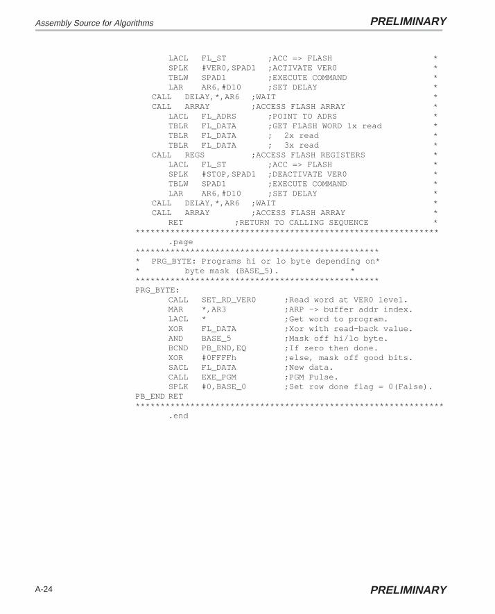
Assembly Source for Algorithms PRELIMINARY
A-24 PRELIMINARY
LACL FL_ST ;ACC => FLASH *SPLK #VER0,SPAD1 ;ACTIVATE VER0 *TBLW SPAD1 ;EXECUTE COMMAND *LAR AR6,#D10 ;SET DELAY *
CALL DELAY,*,AR6 ;WAIT *CALL ARRAY ;ACCESS FLASH ARRAY *
LACL FL_ADRS ;POINT TO ADRS *TBLR FL_DATA ;GET FLASH WORD 1x read *TBLR FL_DATA ; 2x read *TBLR FL_DATA ; 3x read *
CALL REGS ;ACCESS FLASH REGISTERS *LACL FL_ST ;ACC => FLASH *SPLK #STOP,SPAD1 ;DEACTIVATE VER0 *TBLW SPAD1 ;EXECUTE COMMAND *LAR AR6,#D10 ;SET DELAY *
CALL DELAY,*,AR6 ;WAIT *CALL ARRAY ;ACCESS FLASH ARRAY *
RET ;RETURN TO CALLING SEQUENCE **************************************************************
.page************************************************** PRG_BYTE: Programs hi or lo byte depending on** byte mask (BASE_5). **************************************************PRG_BYTE:
CALL SET_RD_VER0 ;Read word at VER0 level.MAR *,AR3 ;ARP –> buffer addr index.LACL * ;Get word to program.XOR FL_DATA ;Xor with read–back value.AND BASE_5 ;Mask off hi/lo byte.BCND PB_END,EQ ;If zero then done.XOR #0FFFFh ;else, mask off good bits.SACL FL_DATA ;New data.CALL EXE_PGM ;PGM Pulse.SPLK #0,BASE_0 ;Set row done flag = 0(False).
PB_END RET**************************************************************
.end

Assembly Source for AlgorithmsPRELIMINARY
A-25Assembly Source Listings and Program ExamplesPRELIMINARY
A.1.6 Subroutines Used By All Four Algorithms, SUTILS20.ASM
This assembly file includes two subroutines that change the flash module ac-cess mode and one subroutine that performs software delays. More details onthe individual functions are given in the comments.
**************************************************************** Delay And Access Mode Subroutines *** *** TMS320F2XX Flash Utilities. *** Revision: 2.0, 9/10/97 *** Revision: 2.1, 1/31/98 *** *** Filename: sutils20.asm *** *** Called by: These utilities are used by CLEAR,ERASE, *** PROGRAM algorithms written for F2xx *** devices. *** Function: DELAY Delay loop specified by AR6. *** REGS Clears MODE bit of F_ACCESS0/1 to *** access flash module control registers. *** ARRAY Sets MODE bit of F_ACCESS0/1 to access *** the flash array. ****************************************************************
.include ”svar20.h”
.def DELAY,REGS,ARRAY.sect ”DLY”
**************************************Delays as follows: ** LAR AR6,#N 2 Cycles ** CALL DELAY 4 Cycles ** RPT #DLOOP 2*(N+1) Cycles ** NOP DLOOP*(N+1) Cycles ** BANZ DLY_LP 4*N+2 Cycles ** RET 4 Cycles ** –––––––––––––––––––––––– ** = DLOOP(N+1)+6*N+14 Cycles ** Set N and DLOOP appropriately to ** get desired delay. ***************************************DELAY ;AR6 = OUTER LOOP COUNTDLY_LP RPT #DLOOP ;APPROX 5US DELAY
NOPBANZ DLY_LP,*– ;LOOP UNTIL DONERET ;RETURN TO CALLING SEQUENCE.page
*************************************************** REGS Clears MODE bit of F_ACCESS0/1 to *** access flash module control registers. *********************************************************
.sect ”REG”REGS

Assembly Source for Algorithms PRELIMINARY
A-26 PRELIMINARY
SPLK #0000h,SPAD2***********The next instruction is for F240 only*************
.if F24X = 1 ;Assemble for F24X only.OUT SPAD2,F24X_ACCS ;Enable F240 flash reg mode.
;SPAD1 is dummy value..endif
*************************************************************.if F24X = 0 ;Assemble for F206 only.LACC FL_STSUB #4000hBCND reg1,geq ;if address>= 4000h,set
;set reg mode for flash1 arrayOUT SPAD2,F_ACCESS0 ;Change mode of flash0.RET
reg1 OUT SPAD2,F_ACCESS1 ;Change mode of flash1..endifRET ;RETURN TO CALLING SEQUENCE
.page***************************************************** ARRAY Sets MODE bit of F_ACCESS0/1 to access *** the flash array. ******************************************************
.sect ”ARY”ARRAY
SPLK #0001h,SPAD2***********The next instruction is for F240 only*************
.if F24X = 1 ;Assemble for F240 only.IN SPAD1,F24X_ACCS ;Enable F240 flash array mode.
;SPAD1 is dummy value..endif
*************************************************************.if F24X = 0 ;Assemble for F206 only.LACC FL_STSUB #4000hBCND ary1,geq ;if address>= 4000h,set
;set reg mode for flash1 arrayOUT SPAD2,F_ACCESS0 ;Change mode of flash0.RET
ary1 OUT SPAD2,F_ACCESS1 ;Change mode of flash1..endifRET ;RETURN TO CALLING SEQUENCE
.end

C-Callable Interface to Flash AlgorithmsPRELIMINARY
A-27Assembly Source Listings and Program ExamplesPRELIMINARY
A.2 C-Callable Interface to Flash Algorithms
The two functions erase() and program() are intended for in-application pro-gramming of the ’F20x/F24x flash module. These functions were written to beC callable, but they can also be called from assembly as long as the C stackcalling convention is used.
****************************************************** This file contains two C–callable functions: ** program(), and erase() ** These functions are used for programming and ** erasing the on–chip flash EEPROM of the ’F2XX ** product family. ******************************************************* The functions provide a C–callable, interface to ** the standard ’F2XX flash algorithms. They can ** also be used from assembly code, as long as the ** C stack calling convention is used. Since the ** standard flash algorithms are actually used to ** perform the various flash operations, they must ** must be combined with this code at link time. ** ** The erase function includes all the operations ** (clear+erase+flw) required to prepare the flash ** for programming. In addition to providing the ** C–callable interface, this function is very ** useful since it provides a single call to erase ** the flash memory. ** Since programming the device requires a single ** algorithm, the only purpose for the program() ** function is to provide a C–callable interface. ** The program() function transfers a specified ** block of data memory into a specified, erased ** flash array. ** ** The parameters for each function are described ** in detail below. Note these functions cannot ** reside in the same flash module that they are ** meant to modify. ** ** 10/29/97 Ruben D. Perez ** DSP Applications Team ** Texas Instruments, Inc. ** 03/20/98 Updated for inclusion in flash ** technical reference. ****************************************************
.title ”C–callable Interface to ’F2XX Flash Algorithms**”;**C–callable functions defined in this file.
.global _erase, _program
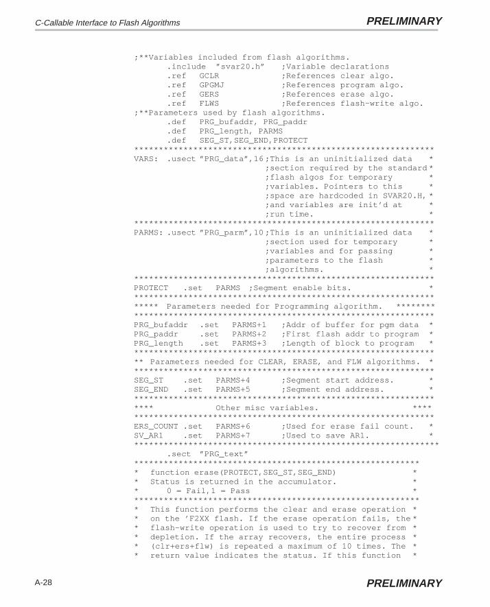
C-Callable Interface to Flash Algorithms PRELIMINARY
A-28 PRELIMINARY
;**Variables included from flash algorithms..include ”svar20.h” ;Variable declarations.ref GCLR ;References clear algo..ref GPGMJ ;References program algo..ref GERS ;References erase algo..ref FLWS ;References flash–write algo.
;**Parameters used by flash algorithms..def PRG_bufaddr, PRG_paddr.def PRG_length, PARMS.def SEG_ST,SEG_END,PROTECT
*************************************************************VARS: .usect ”PRG_data”,16 ;This is an uninitialized data *
;section required by the standard *;flash algos for temporary *;variables. Pointers to this *;space are hardcoded in SVAR20.H, *;and variables are init’d at *;run time. *
*************************************************************PARMS: .usect ”PRG_parm”,10 ;This is an uninitialized data *
;section used for temporary *;variables and for passing *;parameters to the flash *;algorithms. *
*************************************************************PROTECT .set PARMS ;Segment enable bits. ******************************************************************* Parameters needed for Programming algorithm. *********************************************************************PRG_bufaddr .set PARMS+1 ;Addr of buffer for pgm data *PRG_paddr .set PARMS+2 ;First flash addr to program *PRG_length .set PARMS+3 ;Length of block to program **************************************************************** Parameters needed for CLEAR, ERASE, and FLW algorithms. **************************************************************SEG_ST .set PARMS+4 ;Segment start address. *SEG_END .set PARMS+5 ;Segment end address. ****************************************************************** Other misc variables. *****************************************************************ERS_COUNT .set PARMS+6 ;Used for erase fail count. *SV_AR1 .set PARMS+7 ;Used to save AR1. ***************************************************************
.sect ”PRG_text”*********************************************************** function erase(PROTECT,SEG_ST,SEG_END) ** Status is returned in the accumulator. ** 0 = Fail,1 = Pass ************************************************************ This function performs the clear and erase operation ** on the ’F2XX flash. If the erase operation fails, the ** flash–write operation is used to try to recover from ** depletion. If the array recovers, the entire process ** (clr+ers+flw) is repeated a maximum of 10 times. The ** return value indicates the status. If this function *
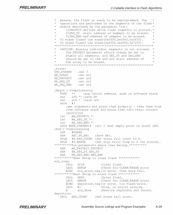
C-Callable Interface to Flash AlgorithmsPRELIMINARY
A-29Assembly Source Listings and Program ExamplesPRELIMINARY
* passes, the flash is ready to be reprogrammed. The ** operations are performed on the segments of the flash ** module described by the parameter list: ** 1)PROTECT–defines which flash segments to protect.** 2)SEG_ST –start address of segment to be erased. ** 3)SEG_END–end address of segment to be erased. ** To erase flash0 use erase(0xff00,0x0000,0x3fff). ** To erase flash1 use erase(0xff00,0x4000,0x7fff). *********************************************************** CAUTION: Erasing individual segments is not allowed. ** The PROTECT parameter should always be set to ** enable all segments, and SEG_ST and SEG_END ** should be set to the end and start address of ** the array to be erased. **********************************************************_erase:ERS_PARAMS .set 3AR_STACK .set ar1AR_PROTECT .set ar2AR_SEG_ST .set ar3AR_SEG_END .set ar4
;Begin C PreprocessingPOPD *+ ;pop return address, push on software stacksar ar0,*+ ;save FPsar ar6,* ;save ar6sbrk #3
;get arguments and place them properly – take them from;the software stack and place them into their correct;positions
lar AR_PROTECT,*–lar AR_SEG_ST,*–lar AR_SEG_END,*–adrk #ERS_PARAMS+4 ;ar1 = next empty point on stack (SP)
;End C PreprocessingLDP #PARMSSAR AR1,SV_AR1 ;Save AR1.SPLK #0,ERS_COUNT ;Set erase fail count to 0.SPLK #0,ERROR ;Set algo error flag to 0 (no errors).
**********Put parameters where they belong.**********SAR AR_PROTECT,PROTECTSAR AR_SEG_ST,SEG_STSAR AR_SEG_END,SEG_END
***********Next Setup to clear flash ************ers_loop:
CALL GCLR ;Clear flash.LACL ERROR ;Check for CLEAR/ERASE errorBCND ers_error,neq ;If error, then hard fail.
***********Next Setup to erase flash ************CALL GERS ;Erase flash.LACL ERROR ;Check for CLEAR/ERASE errorBCND depletion,neq ;If error, try Flash–write.LACL #1 ;Else, no errors erasing.B ers_done ;Restore registers and return.
depletion:LACL ERS_COUNT ;Get erase fail count.

C-Callable Interface to Flash Algorithms PRELIMINARY
A-30 PRELIMINARY
ADD #1 ;Increment fail count.SACL ERS_COUNT ;Save new count.SUB #10 ;CHECK for max of 10.BCND ers_error,GT ;If ers_cout>10 then hard fail.CALL FLWS ;Else, try to recover from depletion.LACL ERROR ;Check for FLASH–WRITE error.BCND ers_error,neq ;If couldn’t recover, then hard fail.B ers_loop ;Else, try erase again.
ers_error:LACL #0 ;Error while erasing.
ers_done:LAR AR1,SV_AR1 ;Restore AR1.CLRC OVM ;Disable overflow.
********************************************;Begin C Post Processing
mar *,ar1sbrk #1lar ar6,*– ;save FPlar ar0,*– ;save ar6pshd * ;pop return address, push on s/w stack
;End C Post Processingret
*****************END of _erase****************************
*********************************************************** function program(PROTECT,PRG_bufaddr,PRG_paddr, ** PRG_length) ** Status will be returned in the accumulator. ** 0 = Fail, 1 = Pass *********************************************************** This function performs the program operation on the ** ’F2XX flash. The values to be programmed will be read ** from a buffer in data memory. The function can program** one to n words of flash in a single call; restricted ** only by the data buffer size. If the function passes, ** the flash was programmed correctly. The function is ** controlled by the following parameter list: ** 1)PROTECT –flash segments to protect. ** 2)PRG_bufaddr –Start address of program buffer in ** data memory. ** 3)PRG_paddr –Start address of flash locations to ** be programmed. ** 4)PRG_length –Number of words to be programmed. ** ** To program 20 words of flash1 starting at address ** 0x4020, from a buffer at 0x0800@data use this: ** program(0xff00,0x0800,0x4020,20). **********************************************************_program:PRG_PARAMS .set 4AR_STACK .set ar1;**Parameters to be popped from s/w stack.AR_PROTECT .set ar2AR_bufaddr .set ar3AR_paddr .set ar4AR_length .set ar5

C-Callable Interface to Flash AlgorithmsPRELIMINARY
A-31Assembly Source Listings and Program ExamplesPRELIMINARY
;Begin C PreprocessingPOPD *+ ; pop return address, push on s/w stacksar ar0,*+ ; save FPsar ar6,* ; save ar6sbrk #3; Local variables (and parameters) are set up as follows:;;get arguments and place them properly – take them from;the software stack and place them into their correct;positionslar AR_PROTECT,*–lar AR_bufaddr,*– lar AR_paddr,*–lar AR_length,*–adrk #PRG_PARAMS+4 ; ar1 = next empty point on stack (SP)
; End C PreprocessingLDP #PARMSSAR AR1,SV_AR1 ;Save AR1.SPLK #0,ERROR ;Set algo error flag to 0
;(no errors).**********Put parameters where they belong.**********
SAR AR_PROTECT,PROTECTSAR AR_bufaddr,PRG_bufaddrSAR AR_paddr,PRG_paddrSAR AR_length,PRG_length
***********Next, program flash ************CALL GPGMJ ;Program flash from buffer.LACL ERROR ;Check for program error.BCND prg_error,neq ;If error then clear ACC.LACL #1 ;Else, No errors programming.B prg_done
prg_error:LACL #0 ;Error while programming.
prg_done:LAR AR1,SV_AR1 ;Restore AR1.CLRC OVM ;Disable overflow.
********************************************;Begin C Post Processing
mar *,ar1sbrk #1lar ar6,*– ;save FPlar ar0,*– ;save ar6pshd * ;pop return address, push on s/w stack
;End C Post Processingret
*****************END of _program************************

Sample Assembly Code to Erase and Reprogram the TMS320F206 PRELIMINARY
A-32 PRELIMINARY
A.3 Sample Assembly Code to Erase and Reprogram the TMS320F206
The algorithm files can be used from assembly in a straightforward manner. Ingeneral, the algorithms can reside anywhere in program space. However, thealgorithms cannot be executed from the flash module that is being modified,and the algorithms must execute with zero wait states. The assembly code andlinker command file in this section provide a working example for the ’F206. Inthis example, the algorithms reside in SARAM, and flash1 is erased and repro-grammed.
A.3.1 Assembly Code for TMS320F206
******************************************************** Filename: ASMEXAMP.ASM ** Description: ** This file contains an example of how to erase ** and program the TMS320F206 flash from assembly ** code using the standard flash algorithm modules. ** The example erases one of the ’F206 flash ** modules, then programs the first three words. ** Since the standard flash algorithms are actually ** used to perform the various flash operations, ** they must must be combined with this code at ** link time. ** ** 03/20/98 Updated for inclusion in flash ** technical reference. ********************************************************
.title ”**Example of Using ’F2XX Flash Algorithms**”;**Variables included from flash algorithms.
.include ”svar20.h” ;Variable declarations
.ref GCLR ;References clear algo.
.ref GPGMJ ;References program algo.
.ref GERS ;References erase algo.
.ref FLWS ;References Flash–write algo.;**Parameters used by flash algorithms.
.def PRG_bufaddr, PRG_paddr
.def PRG_length, PARMS
.def SEG_ST,SEG_END,PROTECT**********************************************************VARS: .usect ”PRG_data”,16 ;This is an uninitialized *
;data section required by *;the standard flash algos *;for temporary variables. *;Pointers to this space *;are hardcoded in SVAR20.H, *;and variables are *;init’d at run time. *
**********************************************************PARMS: .usect ”PRG_parm”,10 ;This is an uninitialized *

Sample Assembly Code to Erase and Reprogram the TMS320F206PRELIMINARY
A-33Assembly Source Listings and Program ExamplesPRELIMINARY
;data section used for *;temporary variables, and *;for passing parameters *;to the flash algorithms. *
*********************************************************PROTECT .set PARMS ;Segment enable bits. **************************************************************Parameters needed for Programming algorithm. *************************************************************PRG_bufaddr .set PARMS+1 ;Address of buffer for *
;program data. *PRG_paddr .set PARMS+2 ;First flash address to *
;program. *PRG_length .set PARMS+3 ;Length of block to program.************************************************************ Parameters needed for CLEAR, ERASE, and FLW algorithms.***********************************************************SEG_ST .set PARMS+4 ;Segment start address. *SEG_END .set PARMS+5 ;Segment end address. *************************************************************** Other misc variables. **************************************************************ERS_COUNT .set PARMS+6 ;Used for erase fail count. ***********************************************************
.text*********************************************************** First, erase flash1 by invoking the clear and erase *** algorithms. *** Note: three parameters must be initialized before *** calling the algorithms. **********************************************************
LDP #PARMSSPLK #0,ERS_COUNT ;Set erase fail count to 0.
**********Put parameters where they belong.**********SPLK #0ff00h,PROTECTSPLK #04000h,SEG_STSPLK #07FFFh,SEG_END
***********First clear flash ************ers_loop:
CALL GCLR ;Clear flash.LACL ERROR ;Check for CLEAR errorBCND ers_error,neq ;If error, then hard fail.
***********Next erase flash ************CALL GERS ;Erase flash.LACL ERROR ;Check for CLEAR errorBCND depletion,neq ;If error, then try
;flash–write.B ers_done ;Else, no errors erasing.
depletion:LACL ERS_COUNT ;Get erase fail count.ADD #1 ;Increment fail count.SACL ERS_COUNT ;Save new count.
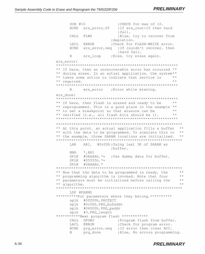
Sample Assembly Code to Erase and Reprogram the TMS320F206 PRELIMINARY
A-34 PRELIMINARY
SUB #10 ;CHECK for max of 10.BCND ers_error,GT ;If ers_cout>10 then hard
;fail.CALL FLWS ;Else, try to recover from
;depletion.LACL ERROR ;Check for FLASH–WRITE error.BCND ers_error,neq ;If couldn’t recover, then
;hard fail.B ers_loop ;Else, try erase again.
ers_error:********************************************************** If here, then an unrecoverable error has occurred **** during erase. In an actual application, the system**** takes some action to indicate that service is **** required. **********************************************************
B ers_error ;Error while erasing.
ers_done:********************************************************** If here, then flash is erased and ready to be **** reprogrammed. This is a good place in the example **** to set a breakpoint so that erasure can be **** verified (i.e., all flash bits should be 1). **********************************************************
************************************************************ At this point, an actual application fills a buffer **** with the data to be programmed. To simulate this in **** the example, three SARAM locations are initialized. ************************************************************
LAR AR1, #0c00h ;Using last 3K of SARAM as;buffer.
MAR *,AR1SPLK #0AAAAh,*+ ;Use dummy data for buffer.SPLK #05555h,*+SPLK #0AAAAh,*
************************************************************ Now that the data to be programmed is ready, the **** programming algorithm is invoked. Note that four **** parameters must be initialized before calling the **** algorithm. ************************************************************
LDP #PARMS**********Put parameters where they belong.**********
splk #0ff00h,PROTECTsplk #0c00h,PRG_bufaddrsplk #04000h,PRG_paddrsplk #3,PRG_length
***********Next program flash ************CALL GPGMJ ;Program flash from buffer.LACL ERROR ;Check for program error.BCND prg_error,neq ;If error then clear ACC.B prg_done ;Else, No errors programming.
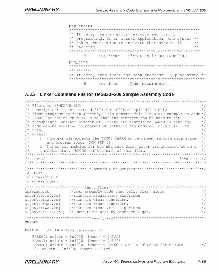
Sample Assembly Code to Erase and Reprogram the TMS320F206PRELIMINARY
A-35Assembly Source Listings and Program ExamplesPRELIMINARY
prg_error:********************************************************** If here, then an error has occurred during **** programming. In an actual application, the system **** takes some action to indicate that service is **** required. **********************************************************
B prg_error ;Error while programming.
prg_done:********************************************************************* If here, then flash has been successfully programmed. ************************************************************
B prg_done ;Done programming.
A.3.2 Linker Command File for TMS320F206 Sample Assembly Code
/********************************************************************************//* Filename: ASMEXAMP.CMD *//* Description: Linker command file for ’F206 example of on–chip *//* flash programming from assembly. This command file links the example to addr *//* 0x8000 of the on–chip SARAM so that the debugger can be used to set *//* breakpoints. Another benefit of linking the example to SARAM is that the *//* code can be modified to operate on either flash module0, or module1, or *//* both. *//* Notes: *//* 1. This example expects the ’F206 SARAM to be mapped in both data space *//* and program space (DON=PON=1). *//* 2. The object modules for the standard flash algos are expected to be in *//* a subdirectory (ALGOS) of the path of this file. *//********************************************************************************//* Rev1.0 3/98 RDP *//********************************************************************************/
/*****************************Command Line Options*******************************/–e .text–o asmexamp.out–m asmexamp.map
/**************************Input Files*******************************************/asmexamp.obj /*User assembly code that calls flash algos. */algos\spgm20.obj /*Standard Programming algorithm. */algos\sclr20.obj /*Standard Clear algorithm. */algos\sera20.obj /*Standard Erase algorithm. */algos\sflw20.obj /*Standard Flash–write algorithm. */algos\sutils20.obj /*Subroutines used by standard algos. */
/*****************************Memory Map*****************************************/MEMORY{PAGE 0: /* PM – Program memory */
FLASH0: origin = 0x0000, length = 0x3fffFLASH1: origin = 0x4000, length = 0x3fffPSARAM: origin = 0x8000, length = 0x400 /*Use 1K of SARAM for PROGRAM */B0: origin = 0xff00, length = 0x1ff
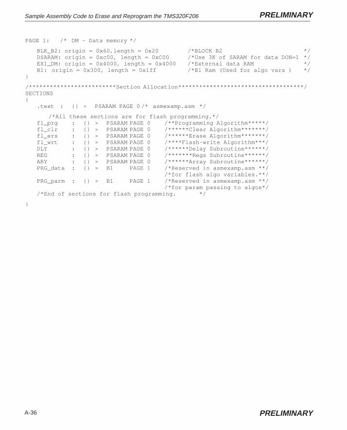
Sample Assembly Code to Erase and Reprogram the TMS320F206 PRELIMINARY
A-36 PRELIMINARY
PAGE 1: /* DM – Data memory */
BLK_B2: origin = 0x60,length = 0x20 /*BLOCK B2 */DSARAM: origin = 0xc00, length = 0xC00 /*Use 3K of SARAM for data DON=1 */EX1_DM: origin = 0x4000, length = 0x4000 /*External data RAM */B1: origin = 0x300, length = 0x1ff /*B1 Ram (Used for algo vars ) */
}
/*************************Section Allocation************************************/SECTIONS{
.text : {} > PSARAM PAGE 0 /* asmexamp.asm */
/*All these sections are for flash programming.*/fl_prg : {} > PSARAM PAGE 0 /**Programming Algorithm*****/fl_clr : {} > PSARAM PAGE 0 /******Clear Algorithm*******/fl_ers : {} > PSARAM PAGE 0 /******Erase Algorithm*******/fl_wrt : {} > PSARAM PAGE 0 /****Flash–write Algorithm***/DLY : {} > PSARAM PAGE 0 /******Delay Subroutine******/REG : {} > PSARAM PAGE 0 /*******Regs Subroutine******/ARY : {} > PSARAM PAGE 0 /******Array Subroutine******/PRG_data : {} > B1 PAGE 1 /*Reserved in asmexamp.asm **/
/*for flash algo variables.**/PRG_parm : {} > B1 PAGE 1 /*Reserved in asmexamp.asm **/
/*for param passing to algos*//*End of sections for flash programming. */
}
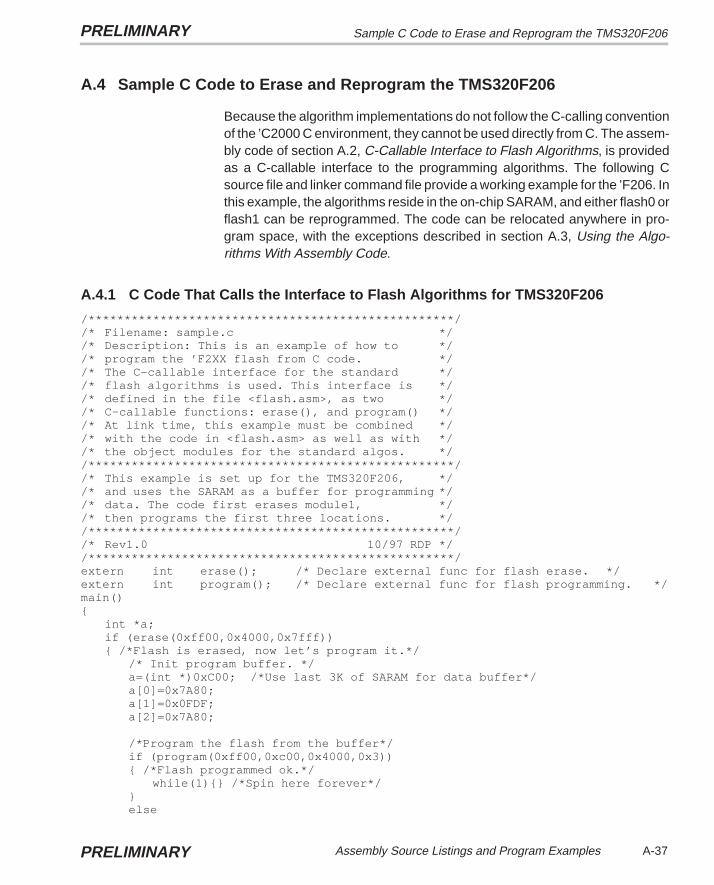
Sample C Code to Erase and Reprogram the TMS320F206PRELIMINARY
A-37Assembly Source Listings and Program ExamplesPRELIMINARY
A.4 Sample C Code to Erase and Reprogram the TMS320F206
Because the algorithm implementations do not follow the C-calling conventionof the ’C2000 C environment, they cannot be used directly from C. The assem-bly code of section A.2, C-Callable Interface to Flash Algorithms, is providedas a C-callable interface to the programming algorithms. The following Csource file and linker command file provide a working example for the ’F206. Inthis example, the algorithms reside in the on-chip SARAM, and either flash0 orflash1 can be reprogrammed. The code can be relocated anywhere in pro-gram space, with the exceptions described in section A.3, Using the Algo-rithms With Assembly Code.
A.4.1 C Code That Calls the Interface to Flash Algorithms for TMS320F206
/***************************************************//* Filename: sample.c *//* Description: This is an example of how to *//* program the ’F2XX flash from C code. *//* The C–callable interface for the standard *//* flash algorithms is used. This interface is *//* defined in the file <flash.asm>, as two *//* C–callable functions: erase(), and program() *//* At link time, this example must be combined *//* with the code in <flash.asm> as well as with *//* the object modules for the standard algos. *//***************************************************//* This example is set up for the TMS320F206, *//* and uses the SARAM as a buffer for programming *//* data. The code first erases module1, *//* then programs the first three locations. *//***************************************************//* Rev1.0 10/97 RDP *//***************************************************/extern int erase(); /* Declare external func for flash erase. */extern int program(); /* Declare external func for flash programming. */main(){
int *a;if (erase(0xff00,0x4000,0x7fff)) { /*Flash is erased, now let’s program it.*/
/* Init program buffer. */ a=(int *)0xC00; /*Use last 3K of SARAM for data buffer*/a[0]=0x7A80;a[1]=0x0FDF;a[2]=0x7A80;
/*Program the flash from the buffer*/if (program(0xff00,0xc00,0x4000,0x3)){ /*Flash programmed ok.*/
while(1){} /*Spin here forever*/}else

Sample C Code to Erase and Reprogram the TMS320F206 PRELIMINARY
A-38 PRELIMINARY
{ /*Flash fails programming, EXIT*/while(1){} /*Spin here forever*/
}} else{ /*Flash fails erase, EXIT*/
while(1){} /*Spin here forever*/}
}
A.4.2 Linker Command File for TMS320F206 Sample C Code
/*************************************************************************//* Filename: F206_SA.CMD *//* Description: Linker command file for ’F206 example of on–chip flash *//* programming from C code. This command file links the *//* example to addr 0x8000 of the on–chip SARAM so that *//* the debugger can be used to set breakpoints. Another *//* benefit of linking the example to SARAM is that the *//* C code can be modified to operate on either flash *//* module0, or module1, or both. *//* Notes: *//* 1. This example expects the ’F206 SARAM to be *//* mapped in both data space and program space *//* (DON=PON=1). *//* 2. The object modules for the standard flash algos *//* are expected to be in a subdirectory (ALGOS) of *//* the path of this file. *//**********************************************************************//* Rev1.0 10/97 RDP *//**********************************************************************/
/************************Command Line Options**************************/–cr /*Use Ram init model. */–heap 0x0 /*No heap needed for this example. */–stack 0x96 /*150–word stack is enough for this example. */–x /*Force rereading of libraries. */–l c:\dsptools\rts2xx.lib–o sample_S.out–m sample_S.map
/*****************************Input Files******************************/sample.obj /*User C code with calls to erase() and program() */flash.obj /*C–callable interface to standard algorithms. */algos\spgm20.obj /*Standard Programming algorithms. */algos\sclr20.obj /*Standard Clear algorithm. */algos\sera20.obj /*Standard Erase algorithm. */algos\sflw20.obj /*Standard Flash–write algorithm. */algos\sutils20.obj /*Subroutines used by standard algorithms. */
/*****************************Memory Map*******************************/MEMORY{PAGE 0: /* PM – Program memory */

Sample C Code to Erase and Reprogram the TMS320F206PRELIMINARY
A-39Assembly Source Listings and Program ExamplesPRELIMINARY
FLASH0: origin = 0x0000, length = 0x3fffFLASH1: origin = 0x4000, length = 0x3fffPSARAM: origin = 0x8000, length = 0x400 /*Use 1K of SARAM for PROGRAM*/B0: origin = 0xff00, length = 0x1ff
PAGE 1: /* DM – Data memory */
BLK_B2: origin = 0x60, length = 0x20 /*BLOCK B2 */DSARAM: origin = 0xc00, length = 0xC00 /*Use 3K of SARAM for data */
/*DON=1*/EX1_DM: origin = 0x4000, length = 0x4000 /*External data RAM */B1: origin = 0x300, length = 0x1ff /*B1 RAM (Used for algo vars )*/
}
/*************************Section Allocation***************************/SECTIONS{
.text : {} > PSARAM PAGE 0 /* sample.c */
/*All these sections are for flash programming.*/PRG_text : {} > PSARAM PAGE 0 /**erase() and program()*****/
/*****from flash.asm file****/fl_prg : {} > PSARAM PAGE 0 /**Programming Algorithm*****/fl_clr : {} > PSARAM PAGE 0 /******Clear Algorithm*******/fl_ers : {} > PSARAM PAGE 0 /******Erase Algorithm*******/fl_wrt : {} > PSARAM PAGE 0 /****Flash–write Algorithm***/DLY : {} > PSARAM PAGE 0 /******Delay Subroutine******/REG : {} > PSARAM PAGE 0 /*******Regs Subroutine******/ARY : {} > PSARAM PAGE 0 /******Array Subroutine******/PRG_data : {} > B1 PAGE 1 /*Reserved in flash.asm for**/
/***flash algo variables.****/PRG_parm : {} > B1 PAGE 1 /*Reserved in flash.asm for**/
/*parameter passing to algos*//*End of sections for flash programming. */
.bss : {} > B1 PAGE 1
.cinit : {} > B1 PAGE 1
.const : {} > B1 PAGE 1
.data : {} > B1 PAGE 1
.stack : {} > B1 PAGE 1 /*C stack. */
}

Sample Assembly Code to Erase and Reprogram the TMS320F240 PRELIMINARY
A-40 PRELIMINARY
A.5 Sample Assembly Code to Erase and Reprogram the TMS320F240
The algorithm files can be used from assembly in a straightforward manner. Ingeneral, the algorithms can reside anywhere in program space. However, thealgorithms cannot be executed from the flash module that is being modified,and the algorithms must execute with zero wait states. The assembly code andlinker command file in this section provide a working example for the ’F240.
Note:
This is not an actual application example since a boot mechanism is requiredto load the external SRAM on powerup. This example uses the ’C2xx C-source Debugger to download the code to the external SRAM. In addition,no reset or interrupt vectors are initialized.
The system requirements are F240 EVM or target board with external pro-gram space SRAM located at 0x8000 and a minumum of 1K words.
A.5.1 Assembly Code for TMS320F240
************************************************************** Filename: ASMEXA24.ASM ** Description: ** This file contains an example of how to erase ** and program the TMS320F240 flash from assembly ** code using the standard flash algorithm modules. ** The example erases the ’F240 flash ** modules, then programs the first three words. ** Since the standard flash algorithms are actually ** used to perform the various flash operations, ** they must must be combined with this code at ** link time. ** ** 03/25/98 Updated for inclusion in flash ** technical reference. **************************************************************
.title ”**Example of Using ’F2XX Flash Algorithms**”

Sample Assembly Code to Erase and Reprogram the TMS320F240PRELIMINARY
A-41Assembly Source Listings and Program ExamplesPRELIMINARY
;**Variables included from flash algorithms..include ”svar20.h” ;Variable declarations.ref GCLR ;References clear algo..ref GPGMJ ;References program algo..ref GERS ;References erase algo..ref FLWS ;References flash–write algo.
;**Parameters used by flash algorithms..def PRG_bufaddr, PRG_paddr.def PRG_length, PARMS.def SEG_ST,SEG_END,PROTECT
;**F240 Register definitionsRTICR .set 07027h ;RTI Control RegisterWDCR .set 07029h ;WD Control RegisterCKCR0 .set 0702Bh ;Clock Control Register 0CKCR1 .set 0702Dh ;Clock Control Register 1SYSSR .set 0701Ah ;System Module Status RegisterDP_PF1 .set 224 ;page 1 of peripheral file
;(7000h/80h)
*************************************************************VARS: .usect ”PRG_data”,16 ;This is an uninitialized data *
;section required by the standard *;flash algos for temporary *;variables. Pointers to this *;space are hardcoded in SVAR20.H, *;and variables are init’d at *;run time. *
*************************************************************PARMS: .usect ”PRG_parm”,10 ;This is an uninitialized data *
;section that is used for *;temporary variables and for *;passing parameters to the flash *;algorithms. *
*************************************************************PROTECT .set PARMS ;Segment enable bits. ******************************************************************** Parameters needed for Programming algorithm. ****************************************************************PRG_bufaddr .set PARMS+1 ;Addr of buffer for pgm data. *PRG_paddr .set PARMS+2 ;1st flash addr to program. *PRG_length .set PARMS+3 ;Length of block to program. ***************************************************************** Parameters needed for CLEAR, ERASE, and FLW algorithms. ***************************************************************SEG_ST .set PARMS+4 ;Segment start address. *SEG_END .set PARMS+5 ;Segment end address. ****************************************************************** Other misc variables. *****************************************************************ERS_COUNT .set PARMS+6 ;Used for erase fail count. **************************************************************
.text*************************************************************** First, initialize the key F240 registers for use with *** the EVM. **************************************************************

Sample Assembly Code to Erase and Reprogram the TMS320F240 PRELIMINARY
A-42 PRELIMINARY
F240INIT: ;Set Data Page pointer to page 1 of the;peripheral frame
LDP #DP_PF1 ;Page DP_PF1 includes WET through *;EINT frames
;initialize WDT registersSPLK #06Fh, WDCR ;clear WDFLAG, Disable WDT
;(if Vpp=5V), set WDT ;for 1 second overflow (max)
SPLK #07h, RTICR ;clear RTI Flag,;set RTI for 1 second overflow;(max)
;EVM 10–MHz oscillator settings.;(XTAL2 open, OSCBYP_=GND)SPLK #00B1h,CKCR1 ;CLKIN(OSC)=10MHz,
;Mult by 2, Div by 1.SPLK #00C3h,CKCR0 ;CLKMD=PLL Enable,SYSCLK=CPUCLK/2
;Clear reset flag bits in SYSSR;(PORRST, PLLRST, ILLRST, SWRST, WDRST)LACL SYSSR ;ACCL <= SYSSRAND #00FFh ;Clear upper 8 bits of SYSSRSACL SYSSR ;Load new value into SYSSR
************************************************************ First, erase flash1 by invoking the clear and erase **** algorithms. **** Note: Three parameters must be initialized before **** calling the algorithms. ************************************************************
LDP #PARMSSPLK #0,ERS_COUNT ;Set erase fail count to 0.
**********Put parameters where they belong.**********SPLK #0ff00h,PROTECTSPLK #00000h,SEG_STSPLK #03FFFh,SEG_END
***********First, clear flash ************
ers_loop:CALL GCLR ;Clear flash.LACL ERROR ;Check for CLEAR/ERASE error
clrerr: BCND ers_error,neq ;If error, then hard fail.***********Next erase flash ************
CALL GERS ;Erase flash.LACL ERROR ;Check for CLEAR/ERASE errorBCND depletion,neq ;If error, then try Flash–write.B ers_done ;Else, no errors erasing.

Sample Assembly Code to Erase and Reprogram the TMS320F240PRELIMINARY
A-43Assembly Source Listings and Program ExamplesPRELIMINARY
depletion:LACL ERS_COUNT ;Get erase fail count.ADD #1 ;Increment fail count.SACL ERS_COUNT ;Save new count.SUB #10 ;CHECK for max of 10.BCND ers_error,GT ;If ers_cout>10 then hard fail.CALL FLWS ;Else, try to recover from
;depletion.LACL ERROR ;Check for FLASH–WRITE error.BCND ers_error,neq ;If couldn’t recover, then hard
;fail.B ers_loop ;Else, Try erase again.
ers_error:**************************************************************** If here, then an unrecoverable error occurred during **** erase. **** In an actual application, the system takes some action **** to indicate that service is required. ****************************************************************
B ers_error ;Error while erasing.
ers_done:************************************************************ If here, then flash is erased and ready to be **** reprogrammed. **** This is a good place in the example to set a **** breakpoint so that erasure can be verified (i.e., **** all flash bits should be 1). ************************************************************
**************************************************************** At this point, an actual application fills a buffer with **** the data to be programmed. To simulate this in the **** example, three DARAM locations are initialized. ****************************************************************
LAR AR1, #0380h ;Using last 128 words of B1 DARAM;as buffer.
MAR *,AR1SPLK #0AAAAh,*+ ;Use dummy data for buffer.SPLK #05555h,*+SPLK #0AAAAh,*

Sample Assembly Code to Erase and Reprogram the TMS320F240 PRELIMINARY
A-44 PRELIMINARY
**************************************************************** Now that the data to be programmed is ready, the **** programming algorithm is invoked. Note: Four parameters **** must be initialized before calling the algorithm. ****************************************************************
LDP #PARMS**********Put parameters where they belong.**********
splk #0ff00h,PROTECTsplk #0380h,PRG_bufaddrsplk #00000h,PRG_paddrsplk #3,PRG_length
***********Next, program flash************CALL GPGMJ ;Program flash from buffer.LACL ERROR ;Check for program error.BCND prg_error,neq ;If error then clear ACC.B prg_done ;Else, No errors programming.
prg_error:************************************************************ If here, then an error occurred during programming. **** In an actual application, the system takes some **** action to indicate that service is required. ************************************************************
B prg_error ;Error while programming.
prg_done:************************************************************ If here, then flash has been successfully programmed. ***********************************************************
B prg_done ;Done programming.

Sample Assembly Code to Erase and Reprogram the TMS320F240PRELIMINARY
A-45Assembly Source Listings and Program ExamplesPRELIMINARY
A.5.2 Linker Command File for TMS320F240 Sample Assembly Code
/************************************************************//* Filename: ASMEXA24.CMD *//* Description: Linker command file for ’F240 example of *//* on–chip flash programming from assembly. This command *//* file links the example to addr 0x8000 of the off–chip *//* pgm RAM, so that the debugger can be used to set *//* breakpoints. *//* Notes: *//* 1. The object modules for the standard flash *//* algos are expected to be in a subdirectory *//* (ALGOS) of the path of this file. *//************************************************************//* Rev1.0 3/98 JGC *//************************************************************/
/*******************Command Line Options*********************/–e .text–o asmexa24.out–m asmexa24.map
/************************Input Files*************************/asmexa24.obj /*User assembly code that calls flash algos. */algos\spgm20.obj /*Standard Programming algorithm. */algos\sclr20.obj /*Standard Clear algorithm. */algos\sera20.obj /*Standard Erase algorithm. */algos\sflw20.obj /*Standard Flash–write algorithm. */algos\sutils20.obj /*Subroutines used by standard algorithms. */
/************************Memory Map**************************/MEMORY{PAGE 0: /* PM – Program memory */
FLASH0: origin = 0x0000, length = 0x4000EXTRAM: origin = 0x8000, length = 0x400 /*Use 1K of Ext. RAM for PROGRAM*/B0PGM: origin = 0xfe00, length = 0x100
PAGE 1: /* DM – Data memory */
BLK_B2: origin = 0x60, length = 0x20 /* BLOCK B2*/EX1_DM: origin = 0x8000, length = 0x4000 /* External data RAM */B0: origin = 0x200, length = 0x100 /* B0 Ram (Used for temp data )*/B1: origin = 0x300, length = 0x100 /* B1 Ram (Used for algo vars )*/
}
/*************************Section Allocation***************************/SECTIONS{
.text :{} > EXTRAM PAGE 0 /* asmexa24.asm */

Sample Assembly Code to Erase and Reprogram the TMS320F240 PRELIMINARY
A-46 PRELIMINARY
/*All these sections are for flash programming.*/fl_prg : {} > EXTRAM PAGE 0 /**Programming Algorithm*****/fl_clr : {} > EXTRAM PAGE 0 /******Clear Algorithm*******/fl_ers : {} > EXTRAM PAGE 0 /******Erase Algorithm*******/fl_wrt : {} > EXTRAM PAGE 0 /****Flash–write Algorithm***/DLY : {} > EXTRAM PAGE 0 /******Delay Subroutine******/REG : {} > EXTRAM PAGE 0 /*******Regs Subroutine******/ARY : {} > EXTRAM PAGE 0 /******Array Subroutine******/PRG_data : {} > B1 PAGE 1 /*Reserved in asmexamp.asm **/
/*for flash algo variables.**/PRG_parm : {} > B1 PAGE 1 /*Reserved in asmexamp.asm **/
/*for param passing to algos*//*End of sections for flash programming. */
}

Using the Algorithms With C Code to Erase and Reprogram the ’F240PRELIMINARY
A-47Assembly Source Listings and Program ExamplesPRELIMINARY
A.6 Using the Algorithms With C Code to Erase and Reprogram the ’F240
Because the algorithm implementations do not follow the C-calling conventionof the ’C2000 C environment, they cannot be used directly from C. The assem-bly code of section A.2, C-Callable Interface to Flash Algorithms, is providedas a C-callable interface to the programming algorithms. The C source file andlinker command file provide a working example for the ’F240.
In this example, the algorithms reside in external SRAM. The code can be relo-cated anywhere in program space, with the exceptions described in sectionA.3, Using the Algorithms With Assembly Code.
Note:
This is not an actual application example since a boot mechanism is requiredto load the external SRAM on powerup. This example uses the ’C2xx C-source Debugger to download the code to the external SRAM. In addition,no reset or interrupt vectors are initialized.
The system requirements are F240 EVM or target board with external pro-gram space SRAM located at 0x8000 and a minimum of 1K words.
A.6.1 C Code That Calls the Interface to Flash Algorithms for TMS320F240
/***********************************************//* Filname: sample24.c *//* Description: This is an example of how to *//* program the ’F2XX flash from C code. *//* The C–callable interface for the standard *//* flash algorithms is used. This interface is *//* defined in the file <flash.asm>, as two *//* C–callable functions: erase(), and program() *//* At link time, this example must be combined *//* with the code in <flash.asm> as well as with *//* the object modules for the standard algos. *//***************************************************//* This example is setup for the TMS320F240, *//* and uses the B1 DARAM as a buffer for program– *//* –ming data. The code first claers, erases, *//* then programs the first three locations. *//***************************************************//* Rev1.0 03/98 JGC *//***************************************************/

Using the Algorithms With C Code to Erase and Reprogram the ’F240 PRELIMINARY
A-48 PRELIMINARY
extern int erase(); /* Declare external func for flash erase. */extern int program(); /* Declare external func for flash programming */extern c240init(); /* Declare external func for C240 register init’l’n */extern wdtoff(); /* Declare external func for wdt disable */main(){
int *a;asm(” CLRC CNF ”); /* map B0 to data space */c240init(); /* initialize key ’240 registers */wdtoff(); /* disable WD timer (works when VCCP=5v) */if (erase(0xff00,0x0000,0x3fff)){ /*Flash is erased, now let’s program it.*/
/* Init program buffer. */a=(int *)0x200; /*Use last 128 words of B1 DARAM for data buffer*/a[0]=0x7A80;a[1]=0x0FDF;a[2]=0x7A80;
/*Program the flash from the buffer*/if (program(0xff00,0x200,0x0000,0x3)){ /*Flash programmed ok.*/
while(1){} /*Spin here forever*/}else{ /*Flash fails programming, EXIT*/
while(1){} /*Spin here forever*/}
} else{ /*Flash fails erase, EXIT*/
while(1){} /*Spin here forever*/}
}
A.6.2 Linker Command File for TMS320F240 Sample C Code
/**********************************************************************//* Filename: F240_EXT.CMD *//* Description: Linker command file for ’F240 example of on–chip flash *//* programming from C–code. This command file links the *//* example to addr 0x8000 of the offchip SRAM, so that *//* the debugger can be used to set breakpoints. *//* Notes: *//* 1. The object modules for the standard flash algos *//* are expected to be in a subdirectory (ALGOS) of *//* the path of this file. *//**********************************************************************//* Rev1.0 03/98 JGC *//**********************************************************************/

Using the Algorithms With C Code to Erase and Reprogram the ’F240PRELIMINARY
A-49Assembly Source Listings and Program ExamplesPRELIMINARY
/************************Command Line Options**************************/–cr /*Use Ram init model. */–heap 0x0 /*No heap needed for this example. */–stack 0x96 /*150 word stack is enough for this example. */–x /*Force re–reading of libraries. */–l c:\dsptools\fix\rts2xx.lib–o sample24.out–m sample24.map
/*****************************Input Files******************************/sample24.obj /*User C–code with calls to erase() and program() */c240init.obj /*C–callabe asm function to init ’240 regs */wdtoff.obj /*C–callable asm function to disable the wdt */flash.obj /*C–callable interface to standard algorithms. */algos\spgm20.obj /*Standard Programming algorithms. */algos\sclr20.obj /*Standard Clear algorithm. */algos\sera20.obj /*Standard Erase algorithm. */algos\sflw20.obj /*Standard Flash–write algorithm. */algos\sutils20.obj /*Subroutines used by standard algorithms. */
/*****************************Memory Map*******************************/MEMORY{PAGE 0: /* PM – Program memory */
FLASH0: origin = 0x0000, length = 0x4000EXTRAM: origin = 0x8000, length = 0x400 /*Use 1K of EXT SRAM for PROGRAM*/B0: origin = 0xfe00, length = 0x100
PAGE 1: /* DM – Data memory */
BLK_B2: origin = 0x60, length = 0x20 /*BLOCK B2 */DSRAM: origin = 0x8000, length = 0x4000 /*External data RAM */B0DAT: origin = 0x200, length = 0x100 /*B0 RAM */
/*(Used for pgm data buffer)*/B1: origin = 0x300, length = 0x100 /* B1 RAM (Used for algo vars )*/
}
/*************************Section Allocation***************************/SECTIONS{
.text :{} > EXTRAM PAGE 0 /* sample.c *//*All these sections are for flash programming.*/PRG_text : {} > EXTRAM PAGE 0 /**erase() and program()*****/
/*****from flash.asm file****/fl_prg : {} > EXTRAM PAGE 0 /**Programming Algorithm*****/fl_clr : {} > EXTRAM PAGE 0 /******Clear Algorithm*******/fl_ers : {} > EXTRAM PAGE 0 /******Erase Algorithm*******/fl_wrt : {} > EXTRAM PAGE 0 /****Flash–write Algorithm***/DLY : {} > EXTRAM PAGE 0 /******Delay Subroutine******/REG : {} > EXTRAM PAGE 0 /*******Regs Subroutine******/ARY : {} > EXTRAM PAGE 0 /******Array Subroutine******/PRG_data : {} > B1 PAGE 1 /*Reserved in flash.asm for**/
/***flash algo variables.****/PRG_parm : {} > B1 PAGE 1 /*Reserved in flash.asm for**/
/*parameter passing to algos*//*End of sections for flash programming. */

Using the Algorithms With C Code to Erase and Reprogram the ’F240 PRELIMINARY
A-50 PRELIMINARY
.bss :{} > B1 PAGE 1
.cinit :{} > B1 PAGE 1
.const : load = EXTRAM PAGE 0, run = DSRAM PAGE 1{
/* GET RUN ADDRESS */__const_run = .;/* MARK LOAD ADDRESS */*(.c_mark)/* ALLOCATE .const */*(.const)/* COMPUTE LENGTH */__const_length = .– __const_run;
}.data :{} > B1 PAGE 1.stack :{} > B1 PAGE 1 /*C stack. */
}
A.6.3 C Function for Disabling TMS320F240 Watchdog Timer
************************************************************************ Watchdog Timer Disable function ** Arguments passed from Caller: None ** Local Variables: None ************************************************************************SYSSR .set 0701Ah ; System Module Status RegisterWDCR .set 07029h ; WDT Control regDP_PF1 .set 224 ; 7000h/80h = 100h or 224
.globl _wdtoff
.text
.def _wdtoff_wdtoff: ; presume ARP = AR1 (SP)****************************************************************************** On entry, presume ARP = AR1 (SP) ** ** Step 1. Pop the return address off the h/w stack and push to s/w stack ******************************************************************************
POPD *+ ; pop return address, push on software stack; ARP=AR1, SP=SP+1
****************************************************************************** Step 2. Push the frame pointer onto s/w stack ******************************************************************************
SAR AR0,*+ ; push AR0 (FP) onto SP; ARP=AR1, SP=SP+2
****************************************************************************** Step 3. Allocate the local frame ******************************************************************************
SAR AR1,* ; *SP = FPLAR AR0,#1 ; FP = size of local frame, 1LAR AR0,*0+ ; FP = SP, SP += size ==> allocate frame
****************************************************************************** Step 5. Begin code that will disable the WDT ******************************************************************************
LDP #DP_PF1 ; Page DP_PF1 includes WET through EINT framesLACL WDCR ; ACC = WDTCR, watchdog timer control register
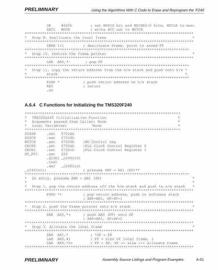
Using the Algorithms With C Code to Erase and Reprogram the ’F240PRELIMINARY
A-51Assembly Source Listings and Program ExamplesPRELIMINARY
OR #06fh ; set WDDIS bit and WDCHK2:0 bits, WDCLK to max.SACL WDCR ; write ACC out to WDTCR
****************************************************************************** Step 9. Deallocate the local frame ******************************************************************************
SBRK 1+1 ; deallocate frame, point to saved FP**************************************************************************** Step 10. restore the frame pointer ******************************************************************************
LAR AR0,*– ; pop FP**************************************************************************** Step 11. copy the return address from the s/w stack and push onto h/w ** stack ****************************************************************************
PSHD * ; push return address on h/w stackRET ; return.en
A.6.4 C Functions for Initializing the TMS320F240
************************************************************************ TMS320x240 Initialization Function ** Arguments passed from Caller: None ** Local Variables: None ************************************************************************SYSSR .set 0701AhSYSCR .set 07018hWDTCR .set 07029h ;WD Control regCKCR0 .set 0702ah ;PLL Clock Control Register 0CKCR1 .set 0702ch ;PLL Clock Control Register 1DP_PF1 .set 224
.globl _c240init
.text
.def _c240init_c240init: ; presume ARP = AR1 (SP)****************************************************************************** On entry, presume ARP = AR1 (SP) ** ** Step 1. pop the return address off the h/w stack and push to s/w stack ******************************************************************************
POPD *+ ; pop return address, push on software stack; ARP=AR1, SP=SP+1
****************************************************************************** Step 2. push the frame pointer onto s/w stack ******************************************************************************
SAR AR0,*+ ; push AR0 (FP) onto SP; ARP=AR1, SP=SP+2
****************************************************************************** Step 3. Allocate the local frame ******************************************************************************
SAR AR1,* ; *SP = FPLAR AR0,#1 ; FP = size of local frame, 1LAR AR0,*0+ ; FP = SP, SP += size ==> allocate frame
*****************************************************************************

Using the Algorithms With C Code to Erase and Reprogram the ’F240 PRELIMINARY
A-52 PRELIMINARY
* Step 5. begin code that will initialize the ’240 registers ******************************************************************************
CLRC SXM ; Clear Sign Extension ModeCLRC OVM ; Reset Overflow Mode
* Set Data Page pointer to page 1 of the peripheral frameLDP #DP_PF1 ; Page DP_PF1 includes WET through EINT frames
* Clear system status register reset bits (PORRST, ILLADR, SWRST, & WDRST)LACL #020h ; load mask pattern to clear rst flagsSACL SYSSR ; write ACC to SYSSR
* Set Watchdog timer period to 1 secondLACL #02Fh ; set WDCHK2 & 0 bits, WDCLK divider to max (1s)SACL WDTCR ; write ACC out to WDTCR
* Configure PLL for 4–MHz xtal, 10–MHz SYSCLK, and 20–MHz CPUCLK* SPLK #00E4h,CKCR1 ;CLKIN(XTAL)=4 MHz,CPUCLK=20 MHz* SPLK #00C3h,CKCR0 ;CLKMD=PLL Enable,SYSCLK=CPUCLK/2* Configure PLL for 10–MHz osc, 10–MHz SYSCLK, and 20–MHz CPUCLK
SPLK #00B1h,CKCR1 ;CLKIN(OSC)=10 MHz,CPUCLK=20 MHzSPLK #00C3h,CKCR0 ;CLKMD=PLL Enable,SYSCLK=CPUCLK/2
* Set VCCAON bit and CLKSRC1:0; leave other bits at their reset values.SPLK #40C8h,SYSCR ; SYSCR <= 40C8h
**************************************************************************** Step 9. Deallocate the local frame ****************************************************************************
SBRK 1+1 ; deallocate frame, point to saved FP**************************************************************************** Step 10. restore the frame pointer ****************************************************************************
LAR AR0,*– ; pop FP**************************************************************************** Step 11. copy the return address from the s/w stack and push onto h/w ** stack ****************************************************************************
PSHD * ; push return address on h/w stackRET ; return.en

IndexPRELIMINARY
Index-1PRELIMINARY
Index
Aaccess modes
code for changing A-25array access 2-5, 2-10, 2-11, 2-16, 3-8register access 2-5, 2-10, 2-11, 3-11
access–control register 2-5 to 2-7modifying in TMS320F206 2-6modifying in TMS320F24x 2-7reading in TMS320F206 2-6
accessing the flash module 2-5address complementing 3-11algorithms
erase 3-10 to 3-13flash–write 3-14 to 3-18in the overall flow 3-2limiting number of bits to be programmed 2-13programming 3-4 to 3-9
applying a single erase pulse 3-11applying a single flash–write pulse 3-15applying a single program pulse 3-8array protection 2-16array segment locations 2-10array size 1-3array–access mode 2-5, 2-10, 2-11, 2-16, 3-8
See also register–access modeassembly source listings
algorithms, variables, and common subrou-tines A-2 to A-26
sample code for TMS320F206 A-32 to A-35sample code for TMS320F240 A-40 to A-44
assistance from TI vii
Bbasic concepts of flash memory 1-2benefits of flash EEPROM 1-1, 1-5
block erase (flash erase) 1-2boot loader code A-1
CC source listings
code that calls the interface to the algo-rithms A-37, A-47
disabling TMS320F240 watchdog timer A-50initializing the TMS320F240 A-51interface to flash algorithms A-27
C–callable interface to flash algorithms A-27charge levels for progamming and erasing 2-4charge margin. See marginclear algorithm code (SCLR2x.ASM) A-5clearing the array (clear operation) 2-14, 2-15code origin for programming and erasing A-1composition of flash module 1-3control registers
accessing 2-5described 2-5 to 2-12
Ddata page pointer initialization A-2data retention 1-2, 2-12delay, in software (code listing) A-25depletion mode
described 2-15inverse–erase read mode 2-12test and detection 2-12, 2-14, 3-15
devices with embedded flash EEPROM 1-3
Eembedded versus discrete flash memory 1-5embedded flash memory described 1-1

Index PRELIMINARY
Index-2 PRELIMINARY
erase algorithmassembly code (SERA2x.ASM) A-10described 3-10 to 3-13flow diagram 3-13in overall flow 3-10
erase() function (C code listing) A-27
erase operationdescribed 2-14following flash–write operation 2-15frequency range 3-12logic levels 2-4role of WDATA 2-11VER1 read mode 2-12verification of erased bits 2-12worst–case voltage for reading erased cell 2-12
erase protection 3-11
erase pulse 2-14
example for TMS320F206assembly code A-32, A-40C code that calls flash.asm A-37, A-47linker command file A-35, A-38, A-45, A-48
execute bit (EXE)described 2-9in mechanism for array protection 2-16location in SEG_CTR register 2-8relation to erase pulse 2-14relation to flash–write pulse 2-15, 3-14relation to program pulse 2-13role in single erase pulse 3-11role in single flash–write pulse 3-15role in single program pulse 3-9
execute key bits (KEY1, KEY0)described 2-9in mechanism for array protection 2-16location in SEG_CTR register 2-8role in single erase pulse 3-11role in single flash–write pulse 3-15role in single program pulse 3-9
extending a read 3-5, 3-17
Fflash memory size 1-3
flash module 1-3
flash operation (block operation) 1-2
flash–write algorithmassembly code (SFLW2x.ASM) A-15described 3-14flow diagram 3-16in overall flow 3-14
flash–write operationdescribed 1-2, 2-15similarity to erase 2-15
flash–write pulse 2-15, 3-14frequency range
erasing 3-12flash–write 3-17programming 3-5
Gglobal parameters in the calling code A-2
Hheader file for constants and variables
(SVAR2x.H) A-2
IIN instruction 2-7inverse–erase read mode 2-12, 2-15, 3-15
KKEY1, KEY0 bits
described 2-9in mechanism for array protection 2-16location in SEG_CTR register 2-8role in single erase pulse 3-11role in single flash–write pulse 3-15role in single program pulse 3-9
Llimited number of bits programmed at one
time 2-13linker command files
for TMS320F206 sample assembly code A-35for TMS320F206 sample C code A-38for TMS320F240 sample assembly code A-45for TMS320F240 sample C code A-48
IndexPRELIMINARY
Index-3PRELIMINARY
Mmargin
determining 3-5, 3-11ensuring data retention 1-2improving 3-12in programming 2-13restoring after flash–write operation 2-15special read modes for ensuring 2-12
masking data in program operation 3-8memory maps 1-4MODE bit 2-6
See also flash access–control registermode selection for access 2-6modifying the array contents 2-2, 2-16module–control register 2-8multiple reads at same location 3-5, 3-17
Nnotational conventions iv
OOUT instruction 2-7over–erasure 2-14, 2-15, 3-14
Pprogram operation
described 2-13frequency range 3-5latching the write address 2-10latching the write data 2-11logic levels 2-4masking off upper or lower bits 2-13specifying write address 2-13VER0 read mode 2-13verification of programmed bits 2-12worst–case voltage for reading programmed
cell 2-12program pulse
applying a series 3-8defined 2-13
program() function (code listing) A-27programming algorithm
assembly code (SPGM2x.ASM) A-19
described 3-4 to 3-9flow diagram 3-6in overall flow 3-4versus clear algorithm 3-2
programming the flash memory. See program opera-tion
protection from unintentional erasure 2-16, 3-11
Rread mode, standard 2-12read modes 2-12reading from the array 2-16recovery from over–erasure 2-15register–access mode 2-5, 2-10, 2-11
See also array–access moderelated documentation vreprogrammability 1-1, 2-14, 2-15, A-1reserving space for code A-2retention of data. See data retention
SSCLR2x.ASM file A-5segment control register (SEG_CTR) 2-8
described 2-8in erase operation 2-14in flash–write operation 2-15in mechanism for array protection 2-16in mode selection 2-6in program operation 2-13relation to flash–write pulse 3-14role in single erase pulse 3-11role in single flash–write pulse 3-15role in single program pulse 3-8
segment enable bits (SEG0–SEG7)described 2-9in mechanism for array protection 2-16location in SEG_CTR register 2-8role in single erase pulse 3-11role in single flash–write pulse 3-15role in single program pulse 3-8
segment locations in array 2-10SERA2x.ASM file (erase algorithm code) A-10SFLW2x.ASM file (flash–write algorithm code A-15space for code A-2SPGM2x.ASM file (program algorithm code) A-19

Index PRELIMINARY
Index-4 PRELIMINARY
subroutines used by all algorithms (SU-TILS2x.ASM) A-25
SUTILS2x.ASM file (code for subroutines) A-25SVAR2x.H file (header file for constants and vari-
ables) A-2
Ttest register (TST) 2-6, 2-8, 2-10
Uuniformity of charge 3-5, 3-9unintentional erasure, protection 2-16using the algorithms with assembly code A-32,
A-40using the algorithms with C code A-37, A-47
Vvariable CPU clock rate 3-5, 3-12, 3-17variable declaration file. See header file for
constants and variables (SVAR2x.H)VCCP pin 2-16, 3-8, 3-11, 3-15VER0 read mode 2-12, 2-13, 3-8, 3-9VER1 read mode 2-12, 2-15, 3-11
verify bits (VER1, VER0)described 2-9location in SEG_CTR register 2-8
voltage level for standard read 2-12
Wweb page iiiworst–case voltage for reading erased cell 2-12worst–case voltage for reading programmed
cell 2-12write address register (WADRS) 2-10
described 2-8in mode selection 2-6in program operation 2-13role in single program pulse 3-8
write data register (WDATA) 2-11described 2-8in mechanism for array protection 2-16in mode selection 2-6in program operation 2-13role in single erase pulse 3-11role in single program pulse 3-8, 3-9
WRITE/ERASE fielddescribed 2-9, 3-8location in SEG_CTR register 2-8role in single erase pulse 3-11role in single flash–write pulse 3-15