tms320vc5402 and tms320uc5402 bootloader (rev. b)
TRANSCRIPT

Application ReportSPRA618B - November 2004
1
TMS320VC5402 and TMS320UC5402 BootloaderRuben D. Perez C5000 Applications
ABSTRACT
This document describes the features and operation of the TMS320UC5402 andTMS320VC5402 bootloader. The contents of the on-chip ROM are also discussed.
Important Notice Regarding Bootloader Program Contents:
Texas Instruments may periodically update the bootloader code supplied in the ROM tocorrect known problems, provide additional features, or improve functionality. Thesechanges may be made without notice, as needed. Although changes to the ROM code willpreserve functional compatibility with prior versions, the locations of functions within the codemay change. Users should avoid calling functions directly from the bootloader codecontained in the ROM, since the code may change in the future.
Contents
1 Introduction 2 . . . . . . . . . . . . . . . . . . . . . . . . . . . . . . . . . . . . . . . . . . . . . . . . . . . . . . . . . . . . . . . . . . . . . . . . 1.1 Bootloader Features 2 . . . . . . . . . . . . . . . . . . . . . . . . . . . . . . . . . . . . . . . . . . . . . . . . . . . . . . . . . . . . . 1.2 On-Chip ROM Description 2 . . . . . . . . . . . . . . . . . . . . . . . . . . . . . . . . . . . . . . . . . . . . . . . . . . . . . . . .
2 Bootloader Operation 3 . . . . . . . . . . . . . . . . . . . . . . . . . . . . . . . . . . . . . . . . . . . . . . . . . . . . . . . . . . . . . . . 2.1 Boot Mode Selection 3 . . . . . . . . . . . . . . . . . . . . . . . . . . . . . . . . . . . . . . . . . . . . . . . . . . . . . . . . . . . . . 2.2 Boot Mode Options 12 . . . . . . . . . . . . . . . . . . . . . . . . . . . . . . . . . . . . . . . . . . . . . . . . . . . . . . . . . . . . .
2.2.1 HPI Boot Mode 12 . . . . . . . . . . . . . . . . . . . . . . . . . . . . . . . . . . . . . . . . . . . . . . . . . . . . . . . . . . 2.2.2 Serial EEPROM Boot Mode 13 . . . . . . . . . . . . . . . . . . . . . . . . . . . . . . . . . . . . . . . . . . . . . . . 2.2.3 Parallel Boot Mode 15 . . . . . . . . . . . . . . . . . . . . . . . . . . . . . . . . . . . . . . . . . . . . . . . . . . . . . . . 2.2.4 Standard Serial Boot Mode 17 . . . . . . . . . . . . . . . . . . . . . . . . . . . . . . . . . . . . . . . . . . . . . . . . 2.2.5 I/O Boot Mode 21 . . . . . . . . . . . . . . . . . . . . . . . . . . . . . . . . . . . . . . . . . . . . . . . . . . . . . . . . . . .
3 Building the Boot Table 22 . . . . . . . . . . . . . . . . . . . . . . . . . . . . . . . . . . . . . . . . . . . . . . . . . . . . . . . . . . . .
List of Figures
Figure 1. Bootloader Mode Selection Process 6 . . . . . . . . . . . . . . . . . . . . . . . . . . . . . . . . . . . . . . . . . . . . . . . Figure 2. I/O Boot Mode 9 . . . . . . . . . . . . . . . . . . . . . . . . . . . . . . . . . . . . . . . . . . . . . . . . . . . . . . . . . . . . . . . . . . Figure 3. HPI Boot Mode Flow 13 . . . . . . . . . . . . . . . . . . . . . . . . . . . . . . . . . . . . . . . . . . . . . . . . . . . . . . . . . . . . Figure 4. McBSP1 to EEPROM Interface for Serial EEPROM Boot Mode 14 . . . . . . . . . . . . . . . . . . . . . . Figure 5. Example Read Access for Serial EEPROM Boot Mode 15 . . . . . . . . . . . . . . . . . . . . . . . . . . . . . . Figure 6. Parallel Boot Mode Process 16 . . . . . . . . . . . . . . . . . . . . . . . . . . . . . . . . . . . . . . . . . . . . . . . . . . . . . Figure 7. Source Program Data Stream for Parallel Boot in 8-,16-Bit-Word Mode 17 . . . . . . . . . . . . . . . . Figure 8. Timing Conditions for Serial Port Boot Operation 18 . . . . . . . . . . . . . . . . . . . . . . . . . . . . . . . . . . . Figure 9. Standard Serial Boot From McBSP1 (8-bit) After BRINT1 = 1 18 . . . . . . . . . . . . . . . . . . . . . . . . Figure 10. Standard Serial Boot From the McBSP0 (16-bit) After BRINT0 = 1 19 . . . . . . . . . . . . . . . . . . . Figure 11. Source Program Data Stream for 8/16-Bit McBSP Boot in Standard Mode 20 . . . . . . . . . . . . Figure 12. I/O Boot Mode Handshake Protocol 21 . . . . . . . . . . . . . . . . . . . . . . . . . . . . . . . . . . . . . . . . . . . . . Figure 13. I/O Boot Mode 22 . . . . . . . . . . . . . . . . . . . . . . . . . . . . . . . . . . . . . . . . . . . . . . . . . . . . . . . . . . . . . . . . Figure 14. Example Command File for Hex Conversion Utility 23 . . . . . . . . . . . . . . . . . . . . . . . . . . . . . . . .

SPRA618B
2 TMS320VC5402 and TMS320UC5402 Bootloader
List of Tables
Table 1. TMS320VC5402 On-chip ROM Program Space 3 . . . . . . . . . . . . . . . . . . . . . . . . . . . . . . . . . . . . . . Table 2. General Structure of Source Program Data Stream in 16-Bit Mode 9 . . . . . . . . . . . . . . . . . . . . . Table 3. General Structure of Source Program Data Stream in 8-Bit Mode 11 . . . . . . . . . . . . . . . . . . . . . .
1 Introduction
This chapter describes the purpose and features of the bootloader on the TMS320UC5402 andTMS320VC5402 (hereafter referred to as C5402) digital signal processors (DSPs). It alsodiscusses the other contents of the device on-chip ROM and identifies where all of thisinformation is located within that memory. Note that some revisions of silicon may exhibitexceptions to the functionality described in this document. Refer to Silicon Updates for theTMS320(UC)VC5402 DSP (TI Literature number SPRZ155) for a complete list of all knownexceptions, and a description of how to determine the revision of a particular device.
1.1 Bootloader Features
The TMS320VC5402 bootloader is used to transfer code from an external source into internal orexternal program memory following power-up. This allows code to reside in slow non-volatilememory externally, and be transferred to high-speed memory to be executed. This eliminatesthe need for mask programming the C5402 internal ROM, which may not be cost effective insome applications.
The bootloader provides a variety of different ways to download code to accommodate differentsystem requirements. This includes multiple types of both parallel bus and serial port bootmodes, as well as bootloading through the HPI, allowing for maximum system flexibility.Bootloading in both 8-bit byte and 16-bit word modes is also supported.
The bootloader uses various control signals including interrupts, BIO, and XF to determine whichboot mode to use. The boot mode selection process, as well as the specifics of bootloaderoperation, are described in detail in section 2 of this document.
1.2 On-Chip ROM Description
On the C5402 device, the on-chip ROM contains several factory programmed sections includingthe bootloader itself and other features. The sections contained in the ROM are:
• Bootloader program. (Described in this document)
• 256-word µlaw and A-law expansion tables. Lookup tables that are used for decoding.
• 256-word sine look-up table. Table consisting of 256 signed Q15 integers, representing360 degrees.
• Factory test code. Reserved code used by TI for testing the device.
• Interrupt vector table. Code that allows indirect vectoring of interrupts.
A listing of all of the C5402 ROM contents are available on the web at:
http://www.ti.com/sc/docs/tools/dsp/ftp/c54x.htm
SPRA618B
3 TMS320VC5402 and TMS320UC5402 Bootloader
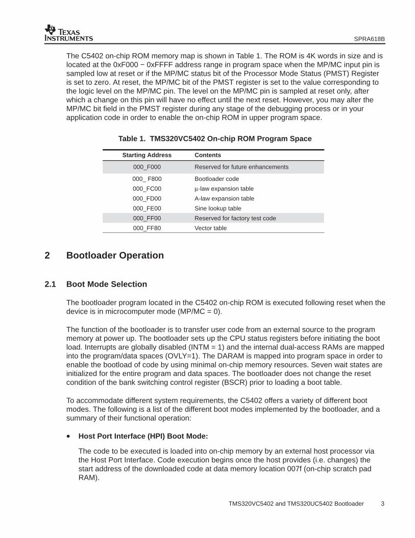
The C5402 on-chip ROM memory map is shown in Table 1. The ROM is 4K words in size and islocated at the 0xF000 − 0xFFFF address range in program space when the MP/MC input pin issampled low at reset or if the MP/MC status bit of the Processor Mode Status (PMST) Registeris set to zero. At reset, the MP/MC bit of the PMST register is set to the value corresponding tothe logic level on the MP/MC pin. The level on the MP/MC pin is sampled at reset only, afterwhich a change on this pin will have no effect until the next reset. However, you may alter theMP/MC bit field in the PMST register during any stage of the debugging process or in yourapplication code in order to enable the on-chip ROM in upper program space.
Table 1. TMS320VC5402 On-chip ROM Program Space
Starting Address Contents
000_F000 Reserved for future enhancements
000_ F800 Bootloader code
000_FC00 µ-law expansion table
000_FD00 A-law expansion table
000_FE00 Sine lookup table
000_FF00 Reserved for factory test code
000_FF80 Vector table
2 Bootloader Operation
2.1 Boot Mode Selection
The bootloader program located in the C5402 on-chip ROM is executed following reset when thedevice is in microcomputer mode (MP/MC = 0).
The function of the bootloader is to transfer user code from an external source to the programmemory at power up. The bootloader sets up the CPU status registers before initiating the bootload. Interrupts are globally disabled (INTM = 1) and the internal dual-access RAMs are mappedinto the program/data spaces (OVLY=1). The DARAM is mapped into program space in order toenable the bootload of code by using minimal on-chip memory resources. Seven wait states areinitialized for the entire program and data spaces. The bootloader does not change the resetcondition of the bank switching control register (BSCR) prior to loading a boot table.
To accommodate different system requirements, the C5402 offers a variety of different bootmodes. The following is a list of the different boot modes implemented by the bootloader, and asummary of their functional operation:
• Host Port Interface (HPI) Boot Mode:
The code to be executed is loaded into on-chip memory by an external host processor viathe Host Port Interface. Code execution begins once the host provides (i.e. changes) thestart address of the downloaded code at data memory location 007f (on-chip scratch padRAM).

SPRA618B
4 TMS320VC5402 and TMS320UC5402 Bootloader
• Parallel Boot Modes (8-bit and 16-bit supported):
The bootloader reads the boot table from data space via the external parallel interface bus.The boot table contains the code sections to be loaded, the destination locations for each ofthe code sections, the execution address once loading is completed, and other configurationinformation.
• Standard Serial Port Boot Modes (8-bit and 16-bit supported):
The bootloader receives the boot table from one of the multi-channel buffered serial ports(McBSP) operating in standard mode, and loads the code according to the informationspecified in the boot table. McBSP0 supports 16-bit serial receive mode. McBSP1 supports8-bit serial receive mode.
• 8-Bit Serial EEPROM Boot Mode:
The bootloader receives the boot table from a serial EEPROM connected to McBSP1operating in clockstop (SPI) mode, and loads the code according to the information specifiedin the boot table.
• I/O Boot Mode (8-bit and 16-bit supported):
The bootloader reads the boot table from I/O port 0h via the external parallel interface busemploying an asynchronous handshake protocol using the XF and BIO pins. This allowsdata transfers to be performed at a rate dictated by the external device.
The bootloader also offers the following additional features:
• Reprogrammable software wait state register
In the parallel and I/O boot modes, the bootloader reconfigures the software wait stateregister based on a value read from the boot table during the bootload.
• Reprogrammable bank switching control register
In the parallel and I/O boot modes, the bootloader reconfigures the bank switching controlregister based on a value read from the boot table during the bootload.
• Multiple-section boot
The C5402 bootloader is capable of loading multiple separate code sections. These sections arenot required to occupy a continuous memory space as in some previous C54x bootloaders.
The details of all of these boot modes are described in the following sections.
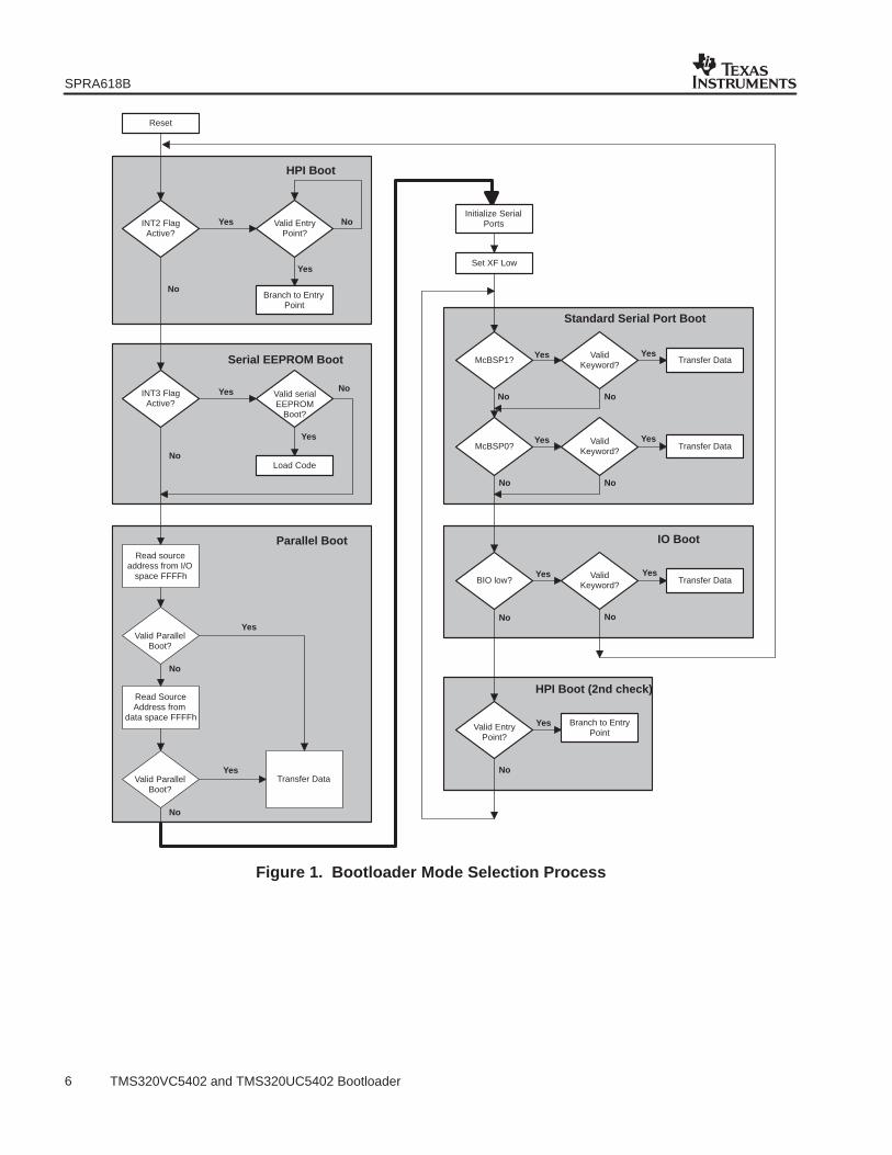
Once the bootloader is initiated, it performs a series of checking operations to determine whichboot mode to use. The bootloader first checks for conditions that indicate it should perform anHPI boot. If the conditions are not met, it goes to the next mode and continues until it finds amode which is selected. The flowchart shown in Figure 1 illustrates the process the bootloaderuses to determine the desired boot mode.

SPRA618B
5 TMS320VC5402 and TMS320UC5402 Bootloader
The bootloader checks each of the boot modes in the following sequence until indications for avalid boot mode are found:
1. Host port interface (HPI) boot mode, first check depending on INT2
2. Serial EEPROM boot mode (8-bit)
3. Parallel boot mode
4. Standard serial boot mode via McBSP1 (8-bit)
5. Standard serial boot mode via McBSP0 (16-bit)
6. I/O boot mode
7. Host port interface (HPI) boot mode, second check depending on entry point
A brief description of each mode is given in this section. Detailed description of the operation ofeach of these boot modes can be found in section 2.2, Boot Mode Options.
SPRA618B
6 TMS320VC5402 and TMS320UC5402 Bootloader
Read sourceaddress from I/O
space FFFFh
Read SourceAddress from
data space FFFFh
Valid ParallelBoot?
Valid ParallelBoot?
Transfer Data
Yes
No
Yes
Parallel Boot
No
McBSP1?Valid
Keyword? Transfer DataYes Yes
No
McBSP0?Valid
Keyword? Transfer DataYes Yes
No
Standard Serial Port Boot
No
No
INT2 FlagActive?
Valid EntryPoint?
Branch to EntryPoint
No
Yes
Yes
HPI Boot
No
BIO low?Valid
Keyword? Transfer DataYes Yes
No
IO Boot
No
Valid EntryPoint?
Branch to EntryPoint
No
HPI Boot (2nd check)
Yes
Reset
Initialize SerialPorts
Set XF Low
INT3 FlagActive?
Valid serialEEPROM
Boot?
Load Code
Yes
Yes
No
Serial EEPROM Boot
No
Figure 1. Bootloader Mode Selection Process

SPRA618B
7 TMS320VC5402 and TMS320UC5402 Bootloader
The first boot mode tested is the HPI boot mode. Unlike some other 54x HPI boot modes, theC5402 HPI boot mode allows the host to load the on-chip RAM after the C5402 is released fromreset. The boot mode also allows the host to specify an entry point at load-time, to define wherethe C5402 begins execution of the loaded code. Immediately after reset, the bootloaderinitializes address 07Fh of the on-chip scratch-pad RAM to zero, and begins polling this locationfor a change in contents. While the C5402 is polling this location, the host can be loading thecode into the on-chip RAM. After completing the bootload process, the host must make anadditional HPI access to load the entry point of the code to location 07Fh. When the bootloaderdetects this change in the contents of address 07Fh, it performs a branch using the contents asthe destination address. Note that because of this polling mechanism, the entry point must be anon-zero value.
Another unique feature of the C5402 HPI boot mode is that it does not require the setting of theinterrupt 2 (INT2) flag for selection. If INT2 is not active, the bootloader periodically checksvarious boot sources, including the polling for HPI boot described above, until a boot condition isdetected. Alternatively, the INT2 flag can be used to force the bootloader to ignore all bootsources other than HPI. If INT2 is found to be active, the bootloader assumes that the code willbe loaded into on-chip RAM by an external host and enters a smaller loop that only performs thepolling described above. If the INT2 flag is not active, the bootloader proceeds to check theSPI EEPROM boot mode.
The serial EEPROM boot mode is checked using the INT3 flag. If INT3 is found to be active, thebootloader assumes that the boot table is located in an 8-bit serial EEPROM connected toMcBSP1. The bootloader reads the value stored at address 0 of the EEPROM. If the value readcontains a valid keyword for the beginning of the boot table, the bootloader proceeds to load theremainder of the boot table from the serial EEPROM. If the INT3 flag is not active, or no validkeyword is found, the bootloader proceeds to check the next boot mode.
The next boot modes tested are the parallel boot modes. The boot table is read from data spaceand can be located at data space addresses between 4000h and FFFFh. The bootloaderdetermines the start address of the boot table by first reading address FFFFh in I/O space. Thebootloader uses the value read from I/O space as the start address of the boot table in dataspace. The beginning of the boot table should contain a certain keyword that indicates whether8-bit or 16-bit boot mode is desired. The valid keyword for 8-bit boot mode is 08AAh (in twoconsecutive 8 bit locations), while the valid keyword for 16-bit boot mode is 10AAh. If no validkeyword is found using the address read from I/O space, the process is repeated using thecontents of address FFFFh of data space. The bootloader reads address FFFFh in data spaceto obtain a start address for the boot table. It then reads the contents of that start address tocheck for a valid keyword. It is convenient to provide both, the start address and the boot table,in data space since this allows storage of both in a single non-volatile memory. When a validkeyword is detected at the start address, the bootloader continues to read the remainder of theboot table and loads and executes the application code. If no valid keyword is found, thebootloader proceeds to check the serial modes.
SPRA618B
8 TMS320VC5402 and TMS320UC5402 Bootloader
Prior to testing for serial or I/O boot modes, the bootloader drives the XF output on the devicelow to indicate that it is ready to receive data. Upon this event, a serial host device may begin tosend the boot table information via McBSP0 or McBSP1. When a word is received on one of theMcBSPs, a serial port interrupt flag will be generated in the C5402. The boot loader uses theseinterrupt flags as indication of which McBSP to use for boot load. The C5402 reads the datareceived on the McBSP and if a valid keyword is found, the boot proceeds with the same serialport and no other boot modes are tested. If neither McBSP responds with received data, thebootloader proceeds to check the I/O boot mode.
In I/O boot mode, the host device makes a request to send data by driving the BIO input to theC5402 low. The bootloader recognizes this request and reads data from I/O port 0000h. If thedata read contains a valid keyword for the beginning of the boot table, the C5402 and the hostproceeds to load the remainder of the boot table using a handshaking scheme as described inSection 2.2.4, I/O Boot Mode.
If a valid boot mode is not found after checking all of the possible boot modes, the bootloaderrestarts and continues to recheck the boot modes, starting with the standard serial port bootmodes. Note that not all boot modes are rechecked.
The flowchart shown in Figure 2 illustrates the basic process the bootloader uses to determinewhether 8- or 16-bit data has been selected, transfer the data, and begin program execution.This process occurs after the bootloader finds what it believes may be a valid boot modeselected. When using the 8-bit boot modes, bytes must be ordered most significant byte first,and for parallel 8-bit modes, the bytes must be presented on the lower-order eight bits of thedata bus. Note that the exact sequence used for 8- and 16-bit mode processing differssomewhat depending on which specific boot mode is selected. The particular sequence used byeach boot mode is shown in the sections describing the different boot modes in detail.

SPRA618B
9 TMS320VC5402 and TMS320UC5402 Bootloader
Yes
No
Data = 10AAh?
I/O boot
Read boot tableand
transfer code
Data = 08h?
Yes
Data =AAh?
Yes
Branch to entry pointand begin
No
No
8-bit I/O mode
16-bit I/O mode
RestartBootLoader
Figure 2. I/O Boot Mode
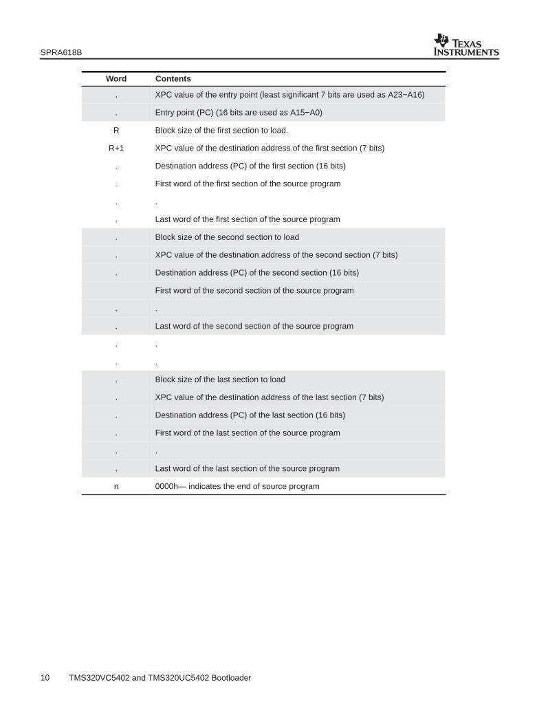
Table 2 and Table 3 show the general structure of the boot table that is loaded for the bootmodes. This structure is the same for all the modes, except HPI, in which code is loaded directlyinto memory and therefore does not require the boot table. The first R−1 words include thekeyword, the words used to initialize the registers (the number of which depends on the bootmode), and the entry point address of the application code. For each load section that follows,there is a word that indicates the block size, followed by two words that indicate the 23-bit loadaddress for the block. When the bootloader encounters a block size of zero (0000h), it branchesto the entry address and begins execution of the application.
Note that these tables are only included to show the basic structure of the boot table. The exactstructure of the boot table varies depending on the boot mode selected. For specific informationabout the structure used by each of the boot modes, refer to the sections describing the differentboot modes in detail.
Table 2. General Structure of Source Program Data Stream in 16-Bit Mode
Word Contents
1 10AAh (memory width of the source program is 16 bits)
2 Value to set in the register (applied to the specified boot mode)
. .
. Value to set in the register
SPRA618B
10 TMS320VC5402 and TMS320UC5402 Bootloader
Word Contents
. XPC value of the entry point (least significant 7 bits are used as A23−A16)
. Entry point (PC) (16 bits are used as A15−A0)
R Block size of the first section to load.
R+1 XPC value of the destination address of the first section (7 bits)
. Destination address (PC) of the first section (16 bits)
. First word of the first section of the source program
. .
. Last word of the first section of the source program
. Block size of the second section to load
. XPC value of the destination address of the second section (7 bits)
. Destination address (PC) of the second section (16 bits)
First word of the second section of the source program
. .
. Last word of the second section of the source program
. .
. .
. Block size of the last section to load
. XPC value of the destination address of the last section (7 bits)
. Destination address (PC) of the last section (16 bits)
. First word of the last section of the source program
. .
. Last word of the last section of the source program
n 0000h— indicates the end of source program

SPRA618B
11 TMS320VC5402 and TMS320UC5402 Bootloader
Table 3. General Structure of Source Program Data Stream in 8-Bit Mode
Byte Contents
1 MSB = 08h, memory width of the source program (8 bits)
2 LSB = 0Aah
3 MSB of the value to set in the register
4 LSB of the value to set in the register
. .
. MSB of the value to set in the register
. LSB of the value to set in the register
. MSB of the XPC value of the entry point
. LSB of the XPC value of the entry point (least significant 7 bits are used)
2R−1 MSB of the entry point (PC)
2R LSB of the entry point (PC)
2R+1 MSB of the block size of the first section to load
2R+2 LSB of the block size of the first section to load
2R+3 MSB of the XPC value of the destination address of the first section
2R+4 LSB of the XPC value of the destination address of the first section (7 bits)
2R+5 MSB of the destination address (PC) of the first section
2R+6 LSB of the destination address (PC) of the first section
. MSB of the first word of the first section of the source program
. .
. LSB of the last word of the first section of the source program
. MSB of the block size of the second section to load
. LSB of the block size of the second section to load
. MSB of the XPC value of the destination address of the second section
. LSB of the XPC value of the destination address of the second section (7 bits)
. MSB of the destination address (PC) of the second section
. LSB of the destination address (PC) of the second section
. MSB of the first word of the second section of the source program
. .
. LSB of the last word of the second section of the source program
. .
SPRA618B
12 TMS320VC5402 and TMS320UC5402 Bootloader
Table 3. General Structure of Source Program Data Stream in 8-Bit Mode (Continued)
Byte Contents
. MSB of the block size of the last section to load
. LSB of the block size of the last section to load
. MSB of the XPC value of the destination address of the last section
. LSB of the XPC value of the destination address of the last section (7 bits)
. MSB of the destination address (PC) of the last section
. LSB of the destination address (PC) of the last section
. MSB of the first word of the last section of the source program
. .
. LSB of the last word of the last section of the source program
2n 00h
2n+1 00h indicates the end of the source program
2.2 Boot Mode Options
The following sections discuss each of the bootloader modes and how they are selected andused.
2.2.1 HPI Boot Mode
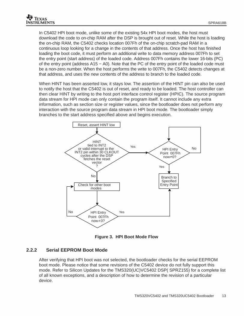
The first boot mode checked after reset is HPI boot mode. After a reset, the bootloader initializesdata memory address 007Fh to 0 and uses it as a software indication for when the host hascompleted loading the application code through the HPI. It then asserts the host interrupt outputsignal (HINT) low. The bootloader checks to see if the INT2 flag in the interrupt flag register(IFR) is equal to 1 (active), and if so, initiates HPI boot mode. The INT2 flag will only be equal toone, if an external user interrupt /INT2 has been detected. This can be accomplished by:
• Tying the HINT output pin directly to the /INT2 input pin, or
• Generating a valid external interrupt on the /INT2 input pin within 30 CPU clock cycles afterthe DSP fetches the reset vector (if HINT is not tied to /INT2)
If the INT2 flag is not set, indicating that the HINT pin is not tied to the INT2 pin or that INT2 isnot asserted within 30 CPU clock cycles, the bootloader checks all boot modes includingHPI mode. If the INT2 flag is set, the bootloader assumes HPI boot mode only and monitors theentry point address as explained below.
SPRA618B
13 TMS320VC5402 and TMS320UC5402 Bootloader
In C5402 HPI boot mode, unlike some of the existing 54x HPI boot modes, the host mustdownload the code to on-chip RAM after the DSP is brought out of reset. While the host is loadingthe on-chip RAM, the C5402 checks location 007Fh of the on-chip scratch-pad RAM in acontinuous loop looking for a change in the contents of that address. Once the host has finishedloading the boot code, it must perform an additional write to data memory address 007Fh to setthe entry point (start address) of the loaded code. Address 007Fh contains the lower 16-bits (PC)of the entry point (address A15 − A0). Note that the PC of the entry point of the loaded code mustbe a non-zero number. When the host performs the write to 007Fh, the C5402 detects changes atthat address, and uses the new contents of the address to branch to the loaded code.
When HINT has been asserted low, it stays low. The assertion of the HINT pin can also be usedto notify the host that the C5402 is out of reset, and ready to be loaded. The host controller canthen clear HINT by writing to the host port interface control register (HPIC). The source programdata stream for HPI mode can only contain the program itself. It cannot include any extrainformation, such as section size or register values, since the bootloader does not perform anyinteraction with the source program data stream in HPI boot mode. The bootloader simplybranches to the start address specified above and begins execution.
Check for other bootmodes
Reset, assert HINT low
No
HINTtied to INT2
or valid interrupt to theINT2 pin within 30 CLKOUT
cycles after the DSPfetches the reset
vector?
Yes
Branch toSpecified
Entry Point
Yes
No
YesNo
HPI EntryPoint 007Fh
now 0?
HPI EntryPoint 007Fh
now 0?≠
≠
Figure 3. HPI Boot Mode Flow
2.2.2 Serial EEPROM Boot Mode
After verifying that HPI boot was not selected, the bootloader checks for the serial EEPROMboot mode. Please notice that some revisions of the C5402 device do not fully support thismode. Refer to Silicon Updates for the TMS320(UC)VC5402 DSP( SPRZ155) for a complete listof all known exceptions, and a description of how to determine the revision of a particulardevice.
SPRA618B
14 TMS320VC5402 and TMS320UC5402 Bootloader
The serial EEPROM boot mode is selected via the /INT3 external interrupt. The bootloaderchecks to see if the INT3 flag in the interrupt flag register (IFR) is equal to 1 (active), and if so,initiates serial EEPROM boot mode. Therefore, proper selection of the boot mode requires ahigh to low transition on the /INT3 pin within 30 CPU cycles after the C5402 is reset. If anexternal event is not available in the system to trigger the interrupt, the McBSP1 transmit pin(BDX1) can be used instead. The BDX1 pin is automatically toggled from high to low within thefirst few cycles after reset, and can be externally connected to the /INT3 input pin to select theboot mode. When the C5402 is reset, the BDX1 pin toggles from high to low causing the /INT3flag to be set, and thereby selecting the serial EEPROM boot mode. This method of selectingthe boot mode is convenient, because it doesn’t require any additional external signals orcomponents.
To summarize, the INT3 flag will be properly activated if:
• The BDX1 pin is tied to the INT3 input pin as shown in Figure 4, or
• A valid interrupt to the INT3 input pin is generated within 30 CPU clock cycles after theDSP fetches the reset vector (if BDX1 is not tied to INT3)
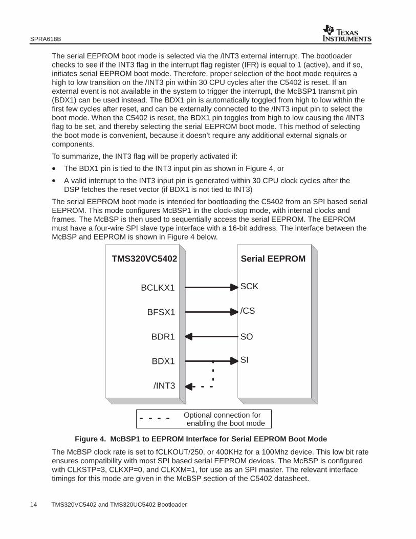
The serial EEPROM boot mode is intended for bootloading the C5402 from an SPI based serialEEPROM. This mode configures McBSP1 in the clock-stop mode, with internal clocks andframes. The McBSP is then used to sequentially access the serial EEPROM. The EEPROMmust have a four-wire SPI slave type interface with a 16-bit address. The interface between theMcBSP and EEPROM is shown in Figure 4 below.
TMS320VC5402
BCLKX1
BFSX1
BDX1
BDR1
/INT3
Serial EEPROM
SCK
/CS
SI
SO
Optional connection forenabling the boot mode
Figure 4. McBSP1 to EEPROM Interface for Serial EEPROM Boot Mode
The McBSP clock rate is set to fCLKOUT/250, or 400KHz for a 100Mhz device. This low bit rateensures compatibility with most SPI based serial EEPROM devices. The McBSP is configuredwith CLKSTP=3, CLKXP=0, and CLKXM=1, for use as an SPI master. The relevant interfacetimings for this mode are given in the McBSP section of the C5402 datasheet.

SPRA618B
15 TMS320VC5402 and TMS320UC5402 Bootloader
For each access, the McBSP transmits a 32-bit packet consisting of the 8-bit read instruction(03h), followed by the 16-bit address to be read from, followed by a “place-holder” byte. TheEEPROM ignores the last 8-bits in the packet, and uses this slot to shift out the addressed byteon the SO output pin. An example read access is shown in Figure 5.
SO / BDR1
BDX1 / SI
BFSX1 / SS
BCLKX1 / SCK
0 0 00 100 A01 A13A14A15 A1A2
D3D7 D4D5D6 D2 D1 D0
Data
AddressEEPROM Instruction
0 7 21654321 1098 31302928272625242322
Figure 5. Example Read Access for Serial EEPROM Boot Mode
The bootloader starts reading from address 0 of the serial EEPROM and checks for a valid boottable. When the bootloader reads and validates the keyword from the beginning of the boottable, it proceeds to read the remainder of the boot table. The serial EEPROM boot mode usesthe same boot table as the standard 8-bit serial boot mode. The bit stream for this boot table isdescribed in Section 2.2.4.
The serial EEPROM boot mode can be used to load multiple sections into any valid programspace address range – including extended program space. Since the serial EEPROM has a16bit address, the maximum possible size of the boot table is 64K bytes, or 32K 16-bit words.This limits the amount of code that can be directly loaded using this boot mode.
After the serial EEPROM boot process completes, the XF signal is toggled low. If the EEPROMhas an active low HOLD input, this event can be used to automatically disable the EEPROMafter bootloading. Note that If no valid keyword is found after the first two reads, the bootprocess is aborted and the bootloader proceeds to check the next boot mode.
2.2.3 Parallel Boot Mode
After verifying that serial EEPROM boot was not selected, the bootloader checks for parallelboot mode. Parallel boot mode reads the desired boot table from data space via the externalparallel interface (external memory interface) and transfers the code to program space. Thebootloader supports parallel boot of 8- or 16-bit wide data. The software wait-state register(SWWSR) and bank-switch control register (BSCR) are reconfigurable in both of these bootmodes. This allows the bootloader to boot from faster EPROM with fewer software wait states.The bootloader uses a default setting of seven wait states.
The bootloader gets the source address from either I/O port 0FFFFh or data memory address0FFFFh. Although either option is valid, it is usually more convenient to provide the sourceaddress at the location in data memory, because then a single nonvolatile memory can containboth the boot table and the entry point.
Since the source address read from either of these locations is 16 bits wide, the boot table canreside in any valid external address range within the data space of C5402 memory map. Thevalid addresses for external data memory on the C5402 are between 04000h and 0FFFFh.Figure 6 shows the sequence of actions in the parallel boot mode.

SPRA618B
16 TMS320VC5402 and TMS320UC5402 Bootloader
NOTE: If a parallel boot is not desired, the data pin D0 of the C5402 can be pulled high with a weakpullup resistor to avoid inadvertently booting from data or I/O space. This will prevent thebootloader from reading the keyword AAh from data space. Otherwise, some other methodshould be used to ensure that a valid keyword in not read unexpectedly.
Figure 6 shows the sequence of actions in the parallel boot mode.
Read first word from the boot table address in data space
Parallel boot
10AAh?
Read 16 bit boot table address from 0FFFFh in I/O space
Read first word from the boot table address in data space
No
16−bit parallel bootmode from data space
Yes
xx08h?
No
Yes xxAAh?
Yes 8−bit parallel bootmode from data space
No
Read 16 bit boot table address from 0FFFFh in data space
10AAh?
No
Yes 16−bit parallel bootmode from data space
Read LSB of the boot table address from 0FFFFh in data spaceRead MSB of the boot table address from 0FFFEh in data space
Check for serial boot modes
Read nextlocation inboot table
xx08h?
No
Yes xxAAh?
Yes 8−bit parallel bootmode from data space
No
Read nextbyte fromboot table
Read first byte from the boot table address in data space
Figure 6. Parallel Boot Mode Process
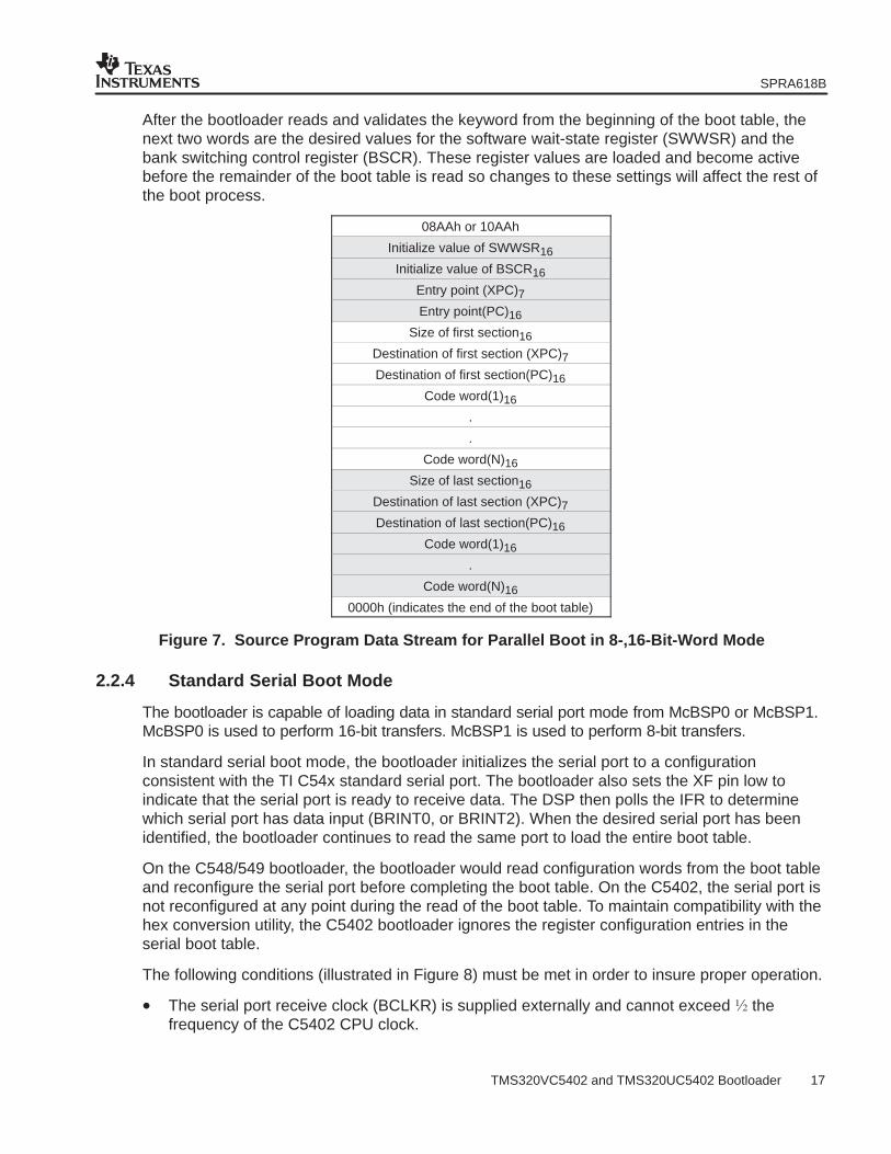
Since the bootloader does not know the memory width before it reads the first word of the boottable, it must check both the data memory LSB (0FFFFh) and MSB (0FFFEh) to obtain thecorrect source address. Figure 7 shows the source program data stream for parallel boot modeusing 8- or 16-bit-word mode.
SPRA618B
17 TMS320VC5402 and TMS320UC5402 Bootloader
After the bootloader reads and validates the keyword from the beginning of the boot table, thenext two words are the desired values for the software wait-state register (SWWSR) and thebank switching control register (BSCR). These register values are loaded and become activebefore the remainder of the boot table is read so changes to these settings will affect the rest ofthe boot process.
08AAh or 10AAh
Initialize value of SWWSR16
Initialize value of BSCR16
Entry point (XPC)7Entry point(PC)16
Size of first section16
Destination of first section (XPC)7Destination of first section(PC)16
Code word(1)16
.
.
Code word(N)16
Size of last section16
Destination of last section (XPC)7Destination of last section(PC)16
Code word(1)16
.
Code word(N)16
0000h (indicates the end of the boot table)
Figure 7. Source Program Data Stream for Parallel Boot in 8-,16-Bit-Word Mode
2.2.4 Standard Serial Boot Mode
The bootloader is capable of loading data in standard serial port mode from McBSP0 or McBSP1.McBSP0 is used to perform 16-bit transfers. McBSP1 is used to perform 8-bit transfers.
In standard serial boot mode, the bootloader initializes the serial port to a configurationconsistent with the TI C54x standard serial port. The bootloader also sets the XF pin low toindicate that the serial port is ready to receive data. The DSP then polls the IFR to determinewhich serial port has data input (BRINT0, or BRINT2). When the desired serial port has beenidentified, the bootloader continues to read the same port to load the entire boot table.
On the C548/549 bootloader, the bootloader would read configuration words from the boot tableand reconfigure the serial port before completing the boot table. On the C5402, the serial port isnot reconfigured at any point during the read of the boot table. To maintain compatibility with thehex conversion utility, the C5402 bootloader ignores the register configuration entries in theserial boot table.
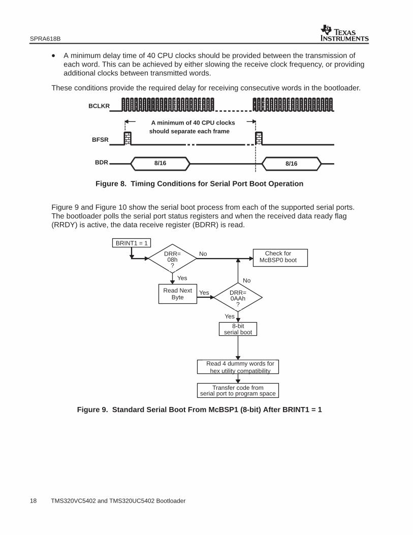
The following conditions (illustrated in Figure 8) must be met in order to insure proper operation.
• The serial port receive clock (BCLKR) is supplied externally and cannot exceed � thefrequency of the C5402 CPU clock.
SPRA618B
18 TMS320VC5402 and TMS320UC5402 Bootloader
• A minimum delay time of 40 CPU clocks should be provided between the transmission ofeach word. This can be achieved by either slowing the receive clock frequency, or providingadditional clocks between transmitted words.
These conditions provide the required delay for receiving consecutive words in the bootloader.
BDR
BFSR
BCLKR
8/168/16
should separate each frameA minimum of 40 CPU clocks
Figure 8. Timing Conditions for Serial Port Boot Operation
Figure 9 and Figure 10 show the serial boot process from each of the supported serial ports.The bootloader polls the serial port status registers and when the received data ready flag(RRDY) is active, the data receive register (BDRR) is read.
BRINT1 = 1
serial boot
DRR=08h?
Yes
Yes
No
DRR=0AAh
?
No
Yes
Transfer code fromserial port to program space
Check forMcBSP0 boot
Read NextByte
Read 4 dummy words forhex utility compatibility
8-bit
Figure 9. Standard Serial Boot From McBSP1 (8-bit) After BRINT1 = 1

SPRA618B
19 TMS320VC5402 and TMS320UC5402 Bootloader
Read 4 dummy wordsFor Hex Utility Compatibility
BRINT0 = 1
Check for I/O bootDRR=10AAh
?
Yes
No
16−bitserial boot
Transfer code fromserial port to program space
Figure 10. Standard Serial Boot From the McBSP0 (16-bit) After BRINT0 = 1
SPRA618B
20 TMS320VC5402 and TMS320UC5402 Bootloader
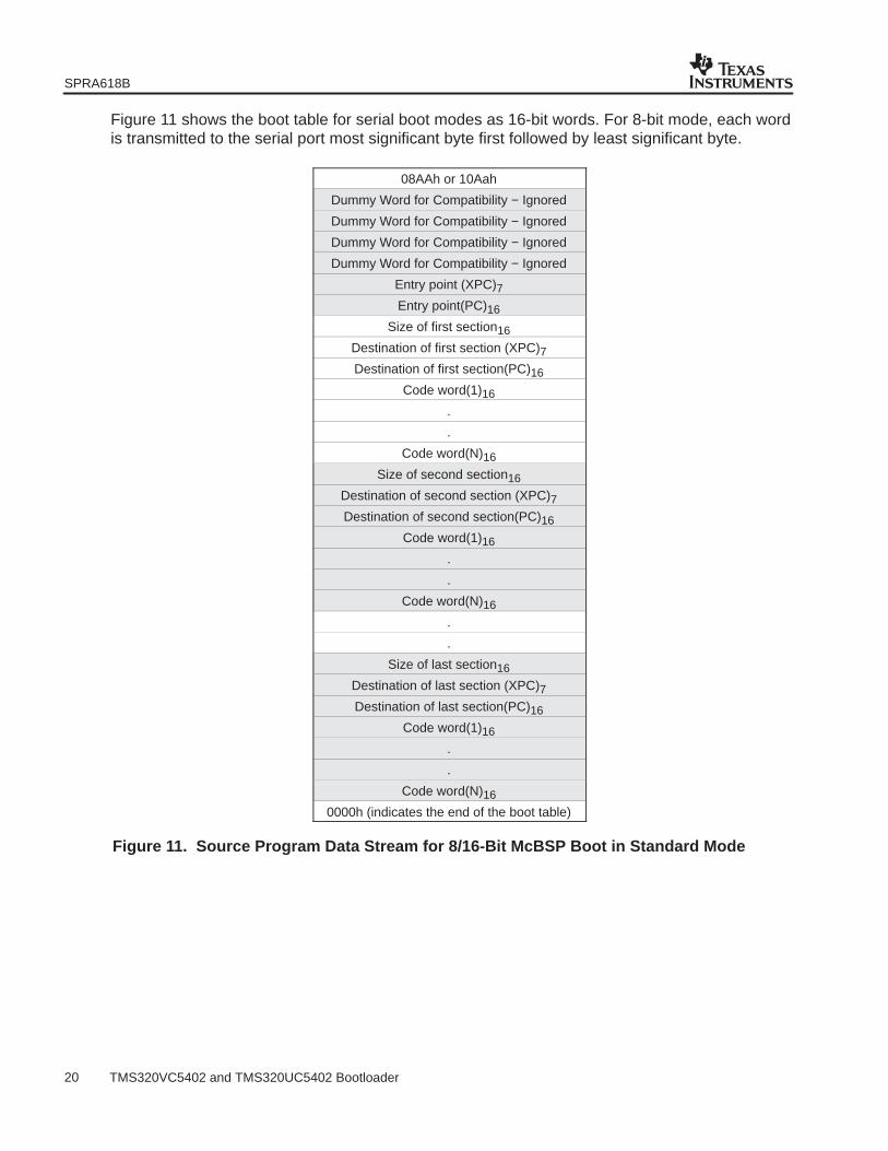
Figure 11 shows the boot table for serial boot modes as 16-bit words. For 8-bit mode, each wordis transmitted to the serial port most significant byte first followed by least significant byte.
08AAh or 10Aah
Dummy Word for Compatibility − Ignored
Dummy Word for Compatibility − Ignored
Dummy Word for Compatibility − Ignored
Dummy Word for Compatibility − Ignored
Entry point (XPC)7Entry point(PC)16
Size of first section16
Destination of first section (XPC)7Destination of first section(PC)16
Code word(1)16
.
.
Code word(N)16
Size of second section16
Destination of second section (XPC)7Destination of second section(PC)16
Code word(1)16
.
.
Code word(N)16
.
.
Size of last section16
Destination of last section (XPC)7Destination of last section(PC)16
Code word(1)16
.
.
Code word(N)16
0000h (indicates the end of the boot table)
Figure 11. Source Program Data Stream for 8/16-Bit McBSP Boot in Standard Mode
SPRA618B
21 TMS320VC5402 and TMS320UC5402 Bootloader
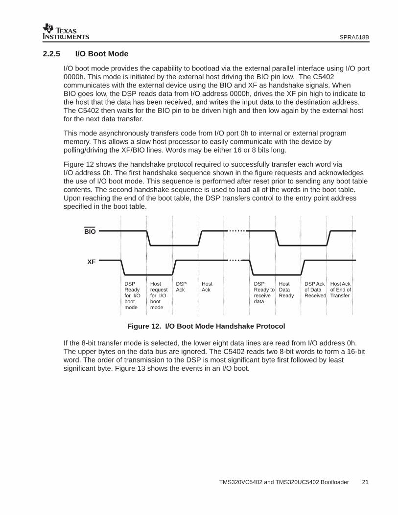
2.2.5 I/O Boot Mode
I/O boot mode provides the capability to bootload via the external parallel interface using I/O port0000h. This mode is initiated by the external host driving the BIO pin low. The C5402communicates with the external device using the BIO and XF as handshake signals. WhenBIO goes low, the DSP reads data from I/O address 0000h, drives the XF pin high to indicate tothe host that the data has been received, and writes the input data to the destination address.The C5402 then waits for the BIO pin to be driven high and then low again by the external hostfor the next data transfer.
This mode asynchronously transfers code from I/O port 0h to internal or external programmemory. This allows a slow host processor to easily communicate with the device bypolling/driving the XF/BIO lines. Words may be either 16 or 8 bits long.
Figure 12 shows the handshake protocol required to successfully transfer each word viaI/O address 0h. The first handshake sequence shown in the figure requests and acknowledgesthe use of I/O boot mode. This sequence is performed after reset prior to sending any boot tablecontents. The second handshake sequence is used to load all of the words in the boot table.Upon reaching the end of the boot table, the DSP transfers control to the entry point addressspecified in the boot table.
DSPReadyfor I/Obootmode
Hostrequestfor I/Obootmode
DSPAck
HostAck
DSPReady toreceivedata
HostDataReady
DSP Ackof DataReceived
Host Ackof End ofTransfer
BIO
XF
Figure 12. I/O Boot Mode Handshake Protocol
If the 8-bit transfer mode is selected, the lower eight data lines are read from I/O address 0h.The upper bytes on the data bus are ignored. The C5402 reads two 8-bit words to form a 16-bitword. The order of transmission to the DSP is most significant byte first followed by leastsignificant byte. Figure 13 shows the events in an I/O boot.

SPRA618B
22 TMS320VC5402 and TMS320UC5402 Bootloader
Yes
No
Data = 10AAh?
I/O boot
Restart bootloader
Read boot tableand
transfer code
Data = 08h?
Yes
Data =AAh?
Yes
Branch to entry pointand begin
No
No
8-bit I/O mode
16-bit I/O mode
Figure 13. I/O Boot Mode
For both 8-bit and 16-bit I/O modes, the structure of the boot table is the same as that shown forthe parallel boot modes in Figure 7.
A minimum delay of ten CPU clock cycles is provided between the XF rising edge and the writeoperation to the destination address. This allows the host processor time to turn off its databuffers before the C5402 initiates a write operation (in case the destination is external memory).Note that the C5402 only drives the external bus when XF is high.
3 Building the Boot Table
To use the features of the C5402 bootloader, you must generate a boot table, which contains thecomplete data stream the bootloader needs. The boot table is generated by the hex conversionutility tool, which is provided with the TMS320C54x Assembly Language Tools Package. Thecontents of the boot table vary, depending on the boot mode and the options selected whenrunning the hex conversion utility.
NOTE: You must use version 1.20 or higher of the C54x code generation tools to generate the proper boot table for the C5402. Previous versions of the code generation tools do not support the enhanced bootloader options for the C5402 and may produce a version of theboot table intended for earlier C54x devices without generating warnings or errors. ContactTexas Instruments for information about upgrades to earlier versions of the code generationtools.
SPRA618B
23 TMS320VC5402 and TMS320UC5402 Bootloader
To build the C5402 boot table, follow these steps:
Step 1: Assemble (or compile) the code using the −v548 assembler option. This optionmarks the object files produced by the assembler specifically for the devices withenhanced bootloader functions including the C5402. The hex conversion utility usesthis information to generate the correct format for the boot table. If this option is notincluded during assembly, the hex conversion utility may produce a version of theboot table intended for earlier C54x devices without generating warnings or errors.
Step 2: Link the file. Each block of the boot table data corresponds to an initialized sectionin the COFF file. Initialized sections include: .text, .const, and .cinit. Uninitializedsections are for example .bss, .stack, and .sysmem. These will not be converted bythe hex conversion utility. It is important to note that sections should not be linkedinto address ranges where no RAM is actually present in the system. For example,no sections should be linked in address ranges 0F000h−0FFFFh, because thisrange of program space is occupied by the on-chip ROM, and cannot be written toby the bootloader.
Step 3: Run the hex conversion utility. Choose the appropriate options for the desiredboot mode and run the hex conversion utility to convert the COFF file produced bythe linker into a boot table. See the TMS320C54x Assembly Language Tools User’sGuide for a detailed description of the procedure for generating a boot table andusing the options.
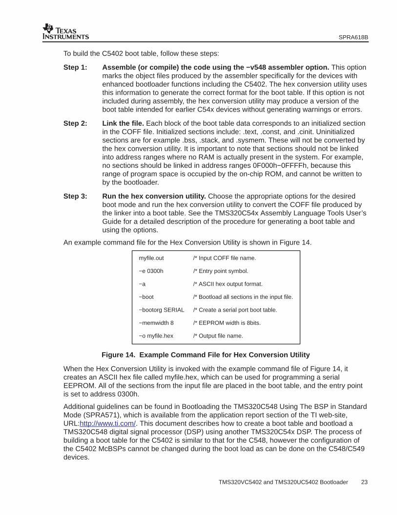
An example command file for the Hex Conversion Utility is shown in Figure 14.
myfile.out /* Input COFF file name.
−e 0300h /* Entry point symbol.
−a /* ASCII hex output format.
−boot /* Bootload all sections in the input file.
−bootorg SERIAL /* Create a serial port boot table.
−memwidth 8 /* EEPROM width is 8bits.
−o myfile.hex /* Output file name.
Figure 14. Example Command File for Hex Conversion Utility
When the Hex Conversion Utility is invoked with the example command file of Figure 14, itcreates an ASCII hex file called myfile.hex, which can be used for programming a serialEEPROM. All of the sections from the input file are placed in the boot table, and the entry pointis set to address 0300h.
Additional guidelines can be found in Bootloading the TMS320C548 Using The BSP in StandardMode (SPRA571), which is available from the application report section of the TI web-site,URL:http://www.ti.com/. This document describes how to create a boot table and bootload aTMS320C548 digital signal processor (DSP) using another TMS320C54x DSP. The process ofbuilding a boot table for the C5402 is similar to that for the C548, however the configuration ofthe C5402 McBSPs cannot be changed during the boot load as can be done on the C548/C549devices.

IMPORTANT NOTICE
Texas Instruments Incorporated and its subsidiaries (TI) reserve the right to make corrections, modifications,enhancements, improvements, and other changes to its products and services at any time and to discontinueany product or service without notice. Customers should obtain the latest relevant information before placingorders and should verify that such information is current and complete. All products are sold subject to TI’s termsand conditions of sale supplied at the time of order acknowledgment.
TI warrants performance of its hardware products to the specifications applicable at the time of sale inaccordance with TI’s standard warranty. Testing and other quality control techniques are used to the extent TIdeems necessary to support this warranty. Except where mandated by government requirements, testing of allparameters of each product is not necessarily performed.
TI assumes no liability for applications assistance or customer product design. Customers are responsible fortheir products and applications using TI components. To minimize the risks associated with customer productsand applications, customers should provide adequate design and operating safeguards.
TI does not warrant or represent that any license, either express or implied, is granted under any TI patent right,copyright, mask work right, or other TI intellectual property right relating to any combination, machine, or processin which TI products or services are used. Information published by TI regarding third-party products or servicesdoes not constitute a license from TI to use such products or services or a warranty or endorsement thereof.Use of such information may require a license from a third party under the patents or other intellectual propertyof the third party, or a license from TI under the patents or other intellectual property of TI.
Reproduction of information in TI data books or data sheets is permissible only if reproduction is withoutalteration and is accompanied by all associated warranties, conditions, limitations, and notices. Reproductionof this information with alteration is an unfair and deceptive business practice. TI is not responsible or liable forsuch altered documentation.
Resale of TI products or services with statements different from or beyond the parameters stated by TI for thatproduct or service voids all express and any implied warranties for the associated TI product or service andis an unfair and deceptive business practice. TI is not responsible or liable for any such statements.
Following are URLs where you can obtain information on other Texas Instruments products and applicationsolutions:
Products Applications
Amplifiers amplifier.ti.com Audio www.ti.com/audio
Data Converters dataconverter.ti.com Automotive www.ti.com/automotive
DSP dsp.ti.com Broadband www.ti.com/broadband
Interface interface.ti.com Digital Control www.ti.com/digitalcontrol
Logic logic.ti.com Military www.ti.com/military
Power Mgmt power.ti.com Optical Networking www.ti.com/opticalnetwork
Microcontrollers microcontroller.ti.com Security www.ti.com/security
Telephony www.ti.com/telephony
Video & Imaging www.ti.com/video
Wireless www.ti.com/wireless
Mailing Address: Texas Instruments
Post Office Box 655303 Dallas, Texas 75265
Copyright 2004, Texas Instruments Incorporated