tms320vc5441 fixed-point digital signal … section describes the main features of the tms320vc5441...
TRANSCRIPT
TMS320VC5441 Fixed-PointDigital Signal Processor
Data Manual
Literature Number: SPRS122FDecember 1999 − Revised October 2008
! !


Revision History
3December 1999 − Revised October 2008 SPRS122F
REVISION HISTORY
This data sheet revision history highlights the technical changes made to the SPRS122E device-specific datasheet to make it an SPRS122F revision.
Scope: This document has been reviewed for technical accuracy; the technical content is up-to-date as of thespecified release date with the following changes.
PAGE(S)NO. ADDITIONS/CHANGES/DELETIONS
17 Table 2−3, Signal Descriptions:− Updated DESCRIPTION of TRST − Added footnote about TRST
85 Section 6, Mechanical Data:− Moved “Package Thermal Resistance Characteristics” section (Section 5.4 in SPRS122E) to Section 6.1− Added Section 6.2, Packaging Information− Mechanical drawings will be appended to this document via an automated process

Revision History
4 December 1999 − Revised October 2008SPRS122F
Contents
5December 1999 − Revised October 2008 SPRS122F
ContentsSection Page
1 TMS320VC5441 Features 11. . . . . . . . . . . . . . . . . . . . . . . . . . . . . . . . . . . . . . . . . . . . . . . . . . . . . . . . . . . . . . . .
2 Introduction 12. . . . . . . . . . . . . . . . . . . . . . . . . . . . . . . . . . . . . . . . . . . . . . . . . . . . . . . . . . . . . . . . . . . . . . . . . . . . 2.1 Description 12. . . . . . . . . . . . . . . . . . . . . . . . . . . . . . . . . . . . . . . . . . . . . . . . . . . . . . . . . . . . . . . . . . . . . . 2.2 Migration From the 5421 to the 5441 13. . . . . . . . . . . . . . . . . . . . . . . . . . . . . . . . . . . . . . . . . . . . . . . . 2.3 Pin Assignments 13. . . . . . . . . . . . . . . . . . . . . . . . . . . . . . . . . . . . . . . . . . . . . . . . . . . . . . . . . . . . . . . . . .
2.3.1 Pin Assignments for the GGU Package 13. . . . . . . . . . . . . . . . . . . . . . . . . . . . . . . . . . . . 2.3.2 Pin Assignments for the PGF Package 15. . . . . . . . . . . . . . . . . . . . . . . . . . . . . . . . . . . . .
2.4 Signal Descriptions 17. . . . . . . . . . . . . . . . . . . . . . . . . . . . . . . . . . . . . . . . . . . . . . . . . . . . . . . . . . . . . . .
3 Functional Overview 23. . . . . . . . . . . . . . . . . . . . . . . . . . . . . . . . . . . . . . . . . . . . . . . . . . . . . . . . . . . . . . . . . . . . 3.1 Memory 24. . . . . . . . . . . . . . . . . . . . . . . . . . . . . . . . . . . . . . . . . . . . . . . . . . . . . . . . . . . . . . . . . . . . . . . . .
3.1.1 Memory Maps 24. . . . . . . . . . . . . . . . . . . . . . . . . . . . . . . . . . . . . . . . . . . . . . . . . . . . . . . . . . 3.1.2 On-Chip Dual-Access RAM (DARAM) 28. . . . . . . . . . . . . . . . . . . . . . . . . . . . . . . . . . . . . . 3.1.3 On-Chip Two-Way Shared RAM 28. . . . . . . . . . . . . . . . . . . . . . . . . . . . . . . . . . . . . . . . . . . 3.1.4 Extended Data Memory 29. . . . . . . . . . . . . . . . . . . . . . . . . . . . . . . . . . . . . . . . . . . . . . . . . . 3.1.5 Extended Program Memory 29. . . . . . . . . . . . . . . . . . . . . . . . . . . . . . . . . . . . . . . . . . . . . . . 3.1.6 Program Memory 29. . . . . . . . . . . . . . . . . . . . . . . . . . . . . . . . . . . . . . . . . . . . . . . . . . . . . . . 3.1.7 Data Memory 29. . . . . . . . . . . . . . . . . . . . . . . . . . . . . . . . . . . . . . . . . . . . . . . . . . . . . . . . . . . 3.1.8 I/O Memory 29. . . . . . . . . . . . . . . . . . . . . . . . . . . . . . . . . . . . . . . . . . . . . . . . . . . . . . . . . . . . 3.1.9 Multicore Reset Signals 30. . . . . . . . . . . . . . . . . . . . . . . . . . . . . . . . . . . . . . . . . . . . . . . . . . 3.1.10 Device Bootload 30. . . . . . . . . . . . . . . . . . . . . . . . . . . . . . . . . . . . . . . . . . . . . . . . . . . . . . . .
3.2 On-Chip Peripherals 30. . . . . . . . . . . . . . . . . . . . . . . . . . . . . . . . . . . . . . . . . . . . . . . . . . . . . . . . . . . . . . 3.2.1 Direct Memory Access (DMA) Controller 30. . . . . . . . . . . . . . . . . . . . . . . . . . . . . . . . . . . 3.2.2 16-Bit Bidirectional Host-Port Interface (HPI16) 34. . . . . . . . . . . . . . . . . . . . . . . . . . . . . . 3.2.3 Multichannel Buffered Serial Port (McBSP) 39. . . . . . . . . . . . . . . . . . . . . . . . . . . . . . . . . 3.2.4 Hardware Timer 43. . . . . . . . . . . . . . . . . . . . . . . . . . . . . . . . . . . . . . . . . . . . . . . . . . . . . . . . . 3.2.5 Watchdog Timer 45. . . . . . . . . . . . . . . . . . . . . . . . . . . . . . . . . . . . . . . . . . . . . . . . . . . . . . . . 3.2.6 Software-Programmable Phase-Locked Loop (PLL) 50. . . . . . . . . . . . . . . . . . . . . . . . . . 3.2.7 General-Purpose I/O 52. . . . . . . . . . . . . . . . . . . . . . . . . . . . . . . . . . . . . . . . . . . . . . . . . . . . 3.2.8 Chip Subsystem ID Register 54. . . . . . . . . . . . . . . . . . . . . . . . . . . . . . . . . . . . . . . . . . . . . . 3.2.9 Data Memory Map Register 54. . . . . . . . . . . . . . . . . . . . . . . . . . . . . . . . . . . . . . . . . . . . . . .
3.3 Memory-Mapped Registers 55. . . . . . . . . . . . . . . . . . . . . . . . . . . . . . . . . . . . . . . . . . . . . . . . . . . . . . . . 3.4 McBSP Control Registers and Subaddresses 57. . . . . . . . . . . . . . . . . . . . . . . . . . . . . . . . . . . . . . . . . 3.5 DMA Subbank Addressed Registers 58. . . . . . . . . . . . . . . . . . . . . . . . . . . . . . . . . . . . . . . . . . . . . . . . . 3.6 Interrupts 60. . . . . . . . . . . . . . . . . . . . . . . . . . . . . . . . . . . . . . . . . . . . . . . . . . . . . . . . . . . . . . . . . . . . . . . . 3.7 IDLE3 Power-Down Mode 62. . . . . . . . . . . . . . . . . . . . . . . . . . . . . . . . . . . . . . . . . . . . . . . . . . . . . . . . . 3.8 Emulating the 5441 Device 62. . . . . . . . . . . . . . . . . . . . . . . . . . . . . . . . . . . . . . . . . . . . . . . . . . . . . . . . .
4 Documentation Support 63. . . . . . . . . . . . . . . . . . . . . . . . . . . . . . . . . . . . . . . . . . . . . . . . . . . . . . . . . . . . . . . .
5 Electrical Specifications 64. . . . . . . . . . . . . . . . . . . . . . . . . . . . . . . . . . . . . . . . . . . . . . . . . . . . . . . . . . . . . . . . 5.1 Absolute Maximum Ratings 64. . . . . . . . . . . . . . . . . . . . . . . . . . . . . . . . . . . . . . . . . . . . . . . . . . . . . . . . 5.2 Recommended Operating Conditions 64. . . . . . . . . . . . . . . . . . . . . . . . . . . . . . . . . . . . . . . . . . . . . . . . 5.3 Electrical Characteristics Over Recommended Operating Case Temperature Range
(Unless Otherwise Noted) 65. . . . . . . . . . . . . . . . . . . . . . . . . . . . . . . . . . . . . . . . . . . . . . . . . . . . . . . . . .

Contents
6 December 1999 − Revised October 2008SPRS122F
Section Page
5.4 Timing Parameter Symbology 66. . . . . . . . . . . . . . . . . . . . . . . . . . . . . . . . . . . . . . . . . . . . . . . . . . . . . . 5.5 Clock Options 67. . . . . . . . . . . . . . . . . . . . . . . . . . . . . . . . . . . . . . . . . . . . . . . . . . . . . . . . . . . . . . . . . . . .
5.5.1 Divide-By-Two, Divide-By-Four, and Bypass Clock Options − PLL Disabled 67. . . . . 5.5.2 Multiply-By-N Clock Option − PLL Enabled 68. . . . . . . . . . . . . . . . . . . . . . . . . . . . . . . . . .
5.6 Reset, x_BIO, and Interrupt Timings 69. . . . . . . . . . . . . . . . . . . . . . . . . . . . . . . . . . . . . . . . . . . . . . . . . 5.7 External Flag (x_XF), Timer (x_TOUT), and Watchdog Timer Output (x_WTOUT) Timings 71. . 5.8 General-Purpose Input/Output (GPIO) Timing 72. . . . . . . . . . . . . . . . . . . . . . . . . . . . . . . . . . . . . . . . 5.9 Multichannel Buffered Serial Port Timing 73. . . . . . . . . . . . . . . . . . . . . . . . . . . . . . . . . . . . . . . . . . . . .
5.9.1 McBSP0/1/2 Transmit and Receive Timings 73. . . . . . . . . . . . . . . . . . . . . . . . . . . . . . . . . 5.9.2 McBSP0 General-Purpose I/O Timing 76. . . . . . . . . . . . . . . . . . . . . . . . . . . . . . . . . . . . . .
5.10 Host-Port Interface (HPI16) Timing 77. . . . . . . . . . . . . . . . . . . . . . . . . . . . . . . . . . . . . . . . . . . . . . . . . .
6 Mechanical Data 85. . . . . . . . . . . . . . . . . . . . . . . . . . . . . . . . . . . . . . . . . . . . . . . . . . . . . . . . . . . . . . . . . . . . . . . . 6.1 Package Thermal Resistance Characteristics 85. . . . . . . . . . . . . . . . . . . . . . . . . . . . . . . . . . . . . . . . . 6.2 Packaging Information 85. . . . . . . . . . . . . . . . . . . . . . . . . . . . . . . . . . . . . . . . . . . . . . . . . . . . . . . . . . . . .

Figures
7December 1999 − Revised October 2008 SPRS122F
List of Figures Figure Page
2−1 169-Ball GGU MicroStar BGA (Bottom View) 13. . . . . . . . . . . . . . . . . . . . . . . . . . . . . . . . . . . . . . . . . . . . .
2−2 176-Pin PGF Low-Profile Quad Flatpack (Top View) 15. . . . . . . . . . . . . . . . . . . . . . . . . . . . . . . . . . . . . .
3−1 Overall Functional Block Diagram 23. . . . . . . . . . . . . . . . . . . . . . . . . . . . . . . . . . . . . . . . . . . . . . . . . . . . . .
3−2 Typical Subsystem Functional Block Diagram 23. . . . . . . . . . . . . . . . . . . . . . . . . . . . . . . . . . . . . . . . . . . .
3−3 Subsystem A CPU Memory Map 24. . . . . . . . . . . . . . . . . . . . . . . . . . . . . . . . . . . . . . . . . . . . . . . . . . . . . . .
3−4 Subsystem B CPU Memory Map 25. . . . . . . . . . . . . . . . . . . . . . . . . . . . . . . . . . . . . . . . . . . . . . . . . . . . . . .
3−5 Subsystem C CPU Memory Map 26. . . . . . . . . . . . . . . . . . . . . . . . . . . . . . . . . . . . . . . . . . . . . . . . . . . . . . .
3−6 Subsystem D CPU Memory Map 27. . . . . . . . . . . . . . . . . . . . . . . . . . . . . . . . . . . . . . . . . . . . . . . . . . . . . . .
3−7 Detailed Memory Map of Local Data Memory Relative to CPU Subsystems A, B, C, and D 28. . . . .
3−8 Subsystem A Local DMA Memory Map 31. . . . . . . . . . . . . . . . . . . . . . . . . . . . . . . . . . . . . . . . . . . . . . . . . .
3−9 Subsystem B Local DMA Memory Map 31. . . . . . . . . . . . . . . . . . . . . . . . . . . . . . . . . . . . . . . . . . . . . . . . . .
3−10 Subsystem C Local DMA Memory Map 32. . . . . . . . . . . . . . . . . . . . . . . . . . . . . . . . . . . . . . . . . . . . . . . . . .
3−11 Subsystem D Local DMA Memory Map 32. . . . . . . . . . . . . . . . . . . . . . . . . . . . . . . . . . . . . . . . . . . . . . . . . .
3−12 Interfacing to the HPI-16 in Non-Multiplexed Mode 36. . . . . . . . . . . . . . . . . . . . . . . . . . . . . . . . . . . . . . . .
3−13 BSCR Register Bit Layout for Subsystem A 37. . . . . . . . . . . . . . . . . . . . . . . . . . . . . . . . . . . . . . . . . . . . . .
3−14 XA Multiplexer for HPI Access 38. . . . . . . . . . . . . . . . . . . . . . . . . . . . . . . . . . . . . . . . . . . . . . . . . . . . . . . . .
3−15 Pin Control Register (PCR) 39. . . . . . . . . . . . . . . . . . . . . . . . . . . . . . . . . . . . . . . . . . . . . . . . . . . . . . . . . . . .
3−16 Multichannel Control Register 2 for McBSPx (MCR2x) 40. . . . . . . . . . . . . . . . . . . . . . . . . . . . . . . . . . . . .
3−17 Multichannel Control Register 1 for McBSPx (MCR1x) 40. . . . . . . . . . . . . . . . . . . . . . . . . . . . . . . . . . . . .
3−18 Receive Channel Enable Registers Bit Layout for Partitions A to H 41. . . . . . . . . . . . . . . . . . . . . . . . . .
3−19 Transmit Channel Enable Registers Bit Layout for Partitions A to H 41. . . . . . . . . . . . . . . . . . . . . . . . .
3−20 SA Multiplexer for McBSP1 Operation 42. . . . . . . . . . . . . . . . . . . . . . . . . . . . . . . . . . . . . . . . . . . . . . . . . .
3−21 Timer Control Register (TCR) 43. . . . . . . . . . . . . . . . . . . . . . . . . . . . . . . . . . . . . . . . . . . . . . . . . . . . . . . . . .
3−22 Timer Second Control Register (TSCR) 45. . . . . . . . . . . . . . . . . . . . . . . . . . . . . . . . . . . . . . . . . . . . . . . . .
3−23 Watchdog Timer Control Register (WDTCR) 46. . . . . . . . . . . . . . . . . . . . . . . . . . . . . . . . . . . . . . . . . . . . .
3−24 Watchdog Timer Second Control Register (WDTSCR) 48. . . . . . . . . . . . . . . . . . . . . . . . . . . . . . . . . . . . .
3−25 Watchdog Operation State Diagram 49. . . . . . . . . . . . . . . . . . . . . . . . . . . . . . . . . . . . . . . . . . . . . . . . . . . .
3−26 Clock Mode Register (CLKMD) 50. . . . . . . . . . . . . . . . . . . . . . . . . . . . . . . . . . . . . . . . . . . . . . . . . . . . . . . . .
3−27 General-Purpose I/O Control Register 53. . . . . . . . . . . . . . . . . . . . . . . . . . . . . . . . . . . . . . . . . . . . . . . . . . .
3−28 Chip Subsystem ID Register (CSIDR) 54. . . . . . . . . . . . . . . . . . . . . . . . . . . . . . . . . . . . . . . . . . . . . . . . . . .
3−29 Data Memory Map Register (DMMR) 54. . . . . . . . . . . . . . . . . . . . . . . . . . . . . . . . . . . . . . . . . . . . . . . . . . .
3−30 Bit Layout of the IMR and IFR Registers for Each Subsystem 61. . . . . . . . . . . . . . . . . . . . . . . . . . . . . .
5−1 3.3-V Test Load Circuit 65. . . . . . . . . . . . . . . . . . . . . . . . . . . . . . . . . . . . . . . . . . . . . . . . . . . . . . . . . . . . . . . .
5−2 External Divide-by-Two Clock Timing 67. . . . . . . . . . . . . . . . . . . . . . . . . . . . . . . . . . . . . . . . . . . . . . . . . . . .
5−3 External Multiply-by-One Clock Timing 68. . . . . . . . . . . . . . . . . . . . . . . . . . . . . . . . . . . . . . . . . . . . . . . . . .
5−4 Reset and x_BIO Timings 69. . . . . . . . . . . . . . . . . . . . . . . . . . . . . . . . . . . . . . . . . . . . . . . . . . . . . . . . . . . . .
5−5 Interrupt Timing 70. . . . . . . . . . . . . . . . . . . . . . . . . . . . . . . . . . . . . . . . . . . . . . . . . . . . . . . . . . . . . . . . . . . . . .

Figures
8 December 1999 − Revised October 2008SPRS122F
Figure Page
5−6 External Flag (x_XF) Timing 71. . . . . . . . . . . . . . . . . . . . . . . . . . . . . . . . . . . . . . . . . . . . . . . . . . . . . . . . . . .
5−7 Timer (x_TOUT) Timing 71. . . . . . . . . . . . . . . . . . . . . . . . . . . . . . . . . . . . . . . . . . . . . . . . . . . . . . . . . . . . . . .
5−8 Watchdog Timer (x_WTOUT) Timing 71. . . . . . . . . . . . . . . . . . . . . . . . . . . . . . . . . . . . . . . . . . . . . . . . . . . .
5−9 GPIO Timings 72. . . . . . . . . . . . . . . . . . . . . . . . . . . . . . . . . . . . . . . . . . . . . . . . . . . . . . . . . . . . . . . . . . . . . . .
5−10 McBSP0/1/2 Receive Timings 75. . . . . . . . . . . . . . . . . . . . . . . . . . . . . . . . . . . . . . . . . . . . . . . . . . . . . . . . . .
5−11 McBSP0/1/2 Transmit Timings 75. . . . . . . . . . . . . . . . . . . . . . . . . . . . . . . . . . . . . . . . . . . . . . . . . . . . . . . . .
5−12 McBSP0 General-Purpose I/O Timings 76. . . . . . . . . . . . . . . . . . . . . . . . . . . . . . . . . . . . . . . . . . . . . . . . . .
5−13 Multiplexed Read Timings Using HAS 79. . . . . . . . . . . . . . . . . . . . . . . . . . . . . . . . . . . . . . . . . . . . . . . . . . .
5−14 Multiplexed Read Timings With HAS Held High 80. . . . . . . . . . . . . . . . . . . . . . . . . . . . . . . . . . . . . . . . . . .
5−15 Multiplexed Write Timings Using HAS 81. . . . . . . . . . . . . . . . . . . . . . . . . . . . . . . . . . . . . . . . . . . . . . . . . . .
5−16 Multiplexed Write Timings With HAS Held High 82. . . . . . . . . . . . . . . . . . . . . . . . . . . . . . . . . . . . . . . . . . .
5−17 Nonmultiplexed Read Timings 83. . . . . . . . . . . . . . . . . . . . . . . . . . . . . . . . . . . . . . . . . . . . . . . . . . . . . . . . . .
5−18 Nonmultiplexed Write Timings 84. . . . . . . . . . . . . . . . . . . . . . . . . . . . . . . . . . . . . . . . . . . . . . . . . . . . . . . . . .
5−19 HPI_SEL1 and HPI_SEL2 Timing 84. . . . . . . . . . . . . . . . . . . . . . . . . . . . . . . . . . . . . . . . . . . . . . . . . . . . . .

Tables
9December 1999 − Revised October 2008 SPRS122F
List of TablesTable Page
2−1 Pin Assignments for TMS320VC5441GGU (169-Ball BGA Package) 14. . . . . . . . . . . . . . . . . . . . . . 2−2 Pin Assignments for TMS320VC5441PGF (176-Pin LQFP Package) 16. . . . . . . . . . . . . . . . . . . . . . 2−3 Signal Descriptions 17. . . . . . . . . . . . . . . . . . . . . . . . . . . . . . . . . . . . . . . . . . . . . . . . . . . . . . . . . . . . . . . . .
3−1 DMA Synchronization Events 34. . . . . . . . . . . . . . . . . . . . . . . . . . . . . . . . . . . . . . . . . . . . . . . . . . . . . . . . . . 3−2 DMA Channel Interrupt Selection 34. . . . . . . . . . . . . . . . . . . . . . . . . . . . . . . . . . . . . . . . . . . . . . . . . . . . . . 3−3 HPI Local/Shared Memory Selection Via HA[20] 35. . . . . . . . . . . . . . . . . . . . . . . . . . . . . . . . . . . . . . . . . 3−4 HPI Local/Shared Memory Selection Via HA[18] 36. . . . . . . . . . . . . . . . . . . . . . . . . . . . . . . . . . . . . . . . . 3−5 BSCR Register Bit Functions for Subsystem A 37. . . . . . . . . . . . . . . . . . . . . . . . . . . . . . . . . . . . . . . . . . 3−6 HPI Module Selection 38. . . . . . . . . . . . . . . . . . . . . . . . . . . . . . . . . . . . . . . . . . . . . . . . . . . . . . . . . . . . . . . . 3−7 Sample Rate Generator Clock Source Selection 40. . . . . . . . . . . . . . . . . . . . . . . . . . . . . . . . . . . . . . . . . 3−8 Receive Channel Enable Registers for Partitions A to H 41. . . . . . . . . . . . . . . . . . . . . . . . . . . . . . . . . . . 3−9 Transmit Channel Enable Registers for Partitions A to H 41. . . . . . . . . . . . . . . . . . . . . . . . . . . . . . . . . . 3−10 TCR Bit Description 44. . . . . . . . . . . . . . . . . . . . . . . . . . . . . . . . . . . . . . . . . . . . . . . . . . . . . . . . . . . . . . . . . . 3−11 TSCR Bit Description 45. . . . . . . . . . . . . . . . . . . . . . . . . . . . . . . . . . . . . . . . . . . . . . . . . . . . . . . . . . . . . . . . 3−12 WDTCR Bit Description 47. . . . . . . . . . . . . . . . . . . . . . . . . . . . . . . . . . . . . . . . . . . . . . . . . . . . . . . . . . . . . . 3−13 WDTSCR Bit Description 48. . . . . . . . . . . . . . . . . . . . . . . . . . . . . . . . . . . . . . . . . . . . . . . . . . . . . . . . . . . . . 3−14 Clock Mode Register (CLKMD) Bit Functions 51. . . . . . . . . . . . . . . . . . . . . . . . . . . . . . . . . . . . . . . . . . . . 3−15 Multiplier Related to PLLNDIV, PLLDIV, and PLLMUL 51. . . . . . . . . . . . . . . . . . . . . . . . . . . . . . . . . . . . . 3−16 VCO Truth Table 51. . . . . . . . . . . . . . . . . . . . . . . . . . . . . . . . . . . . . . . . . . . . . . . . . . . . . . . . . . . . . . . . . . . . . 3−17 VCO Lockup Time 52. . . . . . . . . . . . . . . . . . . . . . . . . . . . . . . . . . . . . . . . . . . . . . . . . . . . . . . . . . . . . . . . . . . 3−18 PLL Initialization at Reset 52. . . . . . . . . . . . . . . . . . . . . . . . . . . . . . . . . . . . . . . . . . . . . . . . . . . . . . . . . . . . . 3−19 General-Purpose I/O Control Register Bit Functions 53. . . . . . . . . . . . . . . . . . . . . . . . . . . . . . . . . . . . . . 3−20 Chip Subsystem ID Register Bit Functions 54. . . . . . . . . . . . . . . . . . . . . . . . . . . . . . . . . . . . . . . . . . . . . . 3−21 Data Memory Map Register Functions 54. . . . . . . . . . . . . . . . . . . . . . . . . . . . . . . . . . . . . . . . . . . . . . . . . . 3−22 Processor Memory-Mapped Registers for Each DSP Subsystem 55. . . . . . . . . . . . . . . . . . . . . . . . . . 3−23 Peripheral Memory-Mapped Registers for Each DSP Subsystem 56. . . . . . . . . . . . . . . . . . . . . . . . . . 3−24 McBSP Control Registers and Subaddresses 57. . . . . . . . . . . . . . . . . . . . . . . . . . . . . . . . . . . . . . . . . . . . 3−25 DMA Subbank Addressed Registers 58. . . . . . . . . . . . . . . . . . . . . . . . . . . . . . . . . . . . . . . . . . . . . . . . . . 3−26 5441 Interrupt Locations and Priorities for Each DSP Subsystem 60. . . . . . . . . . . . . . . . . . . . . . . . . . . 3−27 Bit Functions for IMR and IFR Registers for Each DSP Subsystem 61. . . . . . . . . . . . . . . . . . . . . . . .
5−1 Divide-By-Two, Divide-By-Four, and Bypass Clock Options Timing Requirements 67. . . . . . . . . . . . 5−2 Divide-By-Two, Divide-By-Four, and Bypass Clock Options Switching Characteristics 67. . . . . . . . . 5−3 Multiply-By-N Clock Option Timing Requirements 68. . . . . . . . . . . . . . . . . . . . . . . . . . . . . . . . . . . . . . . . 5−4 Multiply-By-N Clock Option Switching Characteristics 68. . . . . . . . . . . . . . . . . . . . . . . . . . . . . . . . . . . . . 5−5 Reset, x_BIO, and Interrupt Timing Requirements 69. . . . . . . . . . . . . . . . . . . . . . . . . . . . . . . . . . . . . . . . 5−6 External Flag (x_XF), Timer (x_TOUT), and Watchdog Timer Output (x_WTOUT)
Switching Characteristics 71. . . . . . . . . . . . . . . . . . . . . . . . . . . . . . . . . . . . . . . . . . . . . . . . . . . . . . . . . . . . . . 5−7 GPIO Timing Requirements 72. . . . . . . . . . . . . . . . . . . . . . . . . . . . . . . . . . . . . . . . . . . . . . . . . . . . . . . . . . . 5−8 GPIO Switching Characteristics 72. . . . . . . . . . . . . . . . . . . . . . . . . . . . . . . . . . . . . . . . . . . . . . . . . . . . . . . 5−9 McBSP0/1/2 Transmit and Receive Timing Requirements 73. . . . . . . . . . . . . . . . . . . . . . . . . . . . . . . . . 5−10 McBSP0/1/2 Transmit and Receive Switching Characteristics 74. . . . . . . . . . . . . . . . . . . . . . . . . . . . . . 5−11 McBSP0 General-Purpose I/O Timing Requirements 76. . . . . . . . . . . . . . . . . . . . . . . . . . . . . . . . . . . . . 5−12 McBSP0 General-Purpose I/O Switching Characteristics 76. . . . . . . . . . . . . . . . . . . . . . . . . . . . . . . . . .

Tables
10 December 1999 − Revised October 2008SPRS122F
Table Page
5−13 HPI16 Timing Requirements 77. . . . . . . . . . . . . . . . . . . . . . . . . . . . . . . . . . . . . . . . . . . . . . . . . . . . . . . . . . 5−14 HPI16 Switching Characteristics 78. . . . . . . . . . . . . . . . . . . . . . . . . . . . . . . . . . . . . . . . . . . . . . . . . . . . . . .
6−1 Thermal Resistance Characteristics 85. . . . . . . . . . . . . . . . . . . . . . . . . . . . . . . . . . . . . . . . . . . . . . . . . . . .

Features
11December 1999 − Revised October 2008 SPRS122F
1 TMS320VC5441 Features
532-MIPS Quad-Core DSP Consisting ofFour Independent Subsystems
Each Core has an Advanced MultibusArchitecture With Three Separate 16-BitData Memory Buses and One Program Bus
40-Bit Arithmetic Logic Unit (ALU)Including a 40-Bit Barrel-Shifter and Two40-Bit Accumulators Per Core
Each Core has a 17-Bit × 17-Bit ParallelMultiplier Coupled to a 40-Bit Adder forNon-Pipelined Single-Cycle Multiply/Accumulate (MAC) Operations
Each Core has a Compare, Select, andStore Unit (CSSU) for the Add/CompareSelection of the Viterbi Operator
Each Core has an Exponent Encoder toCompute an Exponent Value of a 40-BitAccumulator Value in a Single Cycle
Each Core has Two Address GeneratorsWith Eight Auxiliary Registers and TwoAuxiliary Register Arithmetic Units(ARAUs)
Total 640K-Word × 16-Bit Dual-AccessOn-Chip RAM (256K-Word x 16-Bit SharedMemory and 96K-Word x 16-Bit LocalMemory Per Subsystem)
Single-Instruction Repeat andBlock-Repeat Operations
Instructions With 32-Bit Long WordOperands
Instructions With 2 or 3 Operand Reads
Fast Return From Interrupts
Arithmetic Instructions With Parallel Storeand Parallel Load
Conditional Store Instructions
Output Control of CLKOUT
Output Control of Timer Output (TOUT)
Power Consumption Control With IDLE1,IDLE2, and IDLE3 Instructions
Dual 1.6-V (Core) and 3.3-V (I/O) PowerSupplies for Low-Power, Fast Operations
7.5-ns Single-Cycle Fixed-Point Instruction
Twenty-Four Channels of Direct MemoryAccess (DMA) for Data Transfers With NoCPU Loading (Six Channels PerSubsystem)
Twelve Multichannel Buffered Serial Ports(McBSPs), Each With 128-ChannelSelection Capability (Three McBSPs perSubsystem)
16-Bit Host-Port Interface (HPI)
Software-Programmable Phase-LockedLoop (PLL) Provides Several ClockingOptions (Requires External TTL Oscillator)
On-Chip Scan-Based Emulation Logic,IEEE Standard 1149.1 (JTAG) Boundary-Scan Logic
Four Software-Programmable Timers (One Per Subsystem)
Four Software-Programmable WatchdogTimers (One Per Subsystem)
Sixteen General-Purpose I/Os (Four Per Subsystem)
Provided in 176-pin Plastic Low-ProfileQuad Flatpack (LQFP) Package (PGF Suffix)
Provided in 169-ball MicroStar BGA
Package (GGU Suffix)
MicroStar BGA is a trademark of Texas Instruments.All trademarks are the property of their respective owners.† IEEE Standard 1149.1-1990, Standard Test-Access Port and Boundary Scan Architecture.

Introduction
12 December 1999 − Revised October 2008SPRS122F
2 Introduction
This section describes the main features of the TMS320VC5441 digital signal processor (DSP), lists the pinassignments, and describes the function of each pin. This data manual also provides a detailed descriptionsection, electrical specifications, parameter measurement information, and mechanical data about theavailable packaging.
NOTE: This data manual is designed to be used in conjunction with the TMS320C54x DSP FunctionalOverview (literature number SPRU307).
2.1 Description
The TMS320VC5441 fixed-point digital signal processor is a quad-core solution running at 532-MIPSperformance. The 5441 consists of four DSP subsystems with shared program memory. Each subsystemconsists of one TMS320C54x DSP core, 32K-word program/data DARAM, 64K-word data DARAM, threemultichannel buffered serial ports, DMA logic, one watchdog timer, one general-purpose timer, and othermiscellaneous circuitry.
The 5441 also contains a host-port interface (HPI) that allows the 5441 to be viewed as a memory-mappedperipheral to a host processor.
Each subsystem has its separate program and data spaces, allowing simultaneous accesses to programinstructions and data. Two read operations and one write operation can be performed in one cycle. Instructionswith parallel store and application-specific instructions can fully utilize this architecture. Furthermore, data canbe transferred between program and data spaces. Such parallelism supports a powerful set of arithmetic,logic, and bit-manipulation operations that can all be performed in a single machine cycle. The 5441 includesthe control mechanisms to manage interrupts, repeated operations, and function calls. In addition, the 5441has a total of 256K words of shared program memory (128K words shared by subsystems A and B, andanother 128K words shared by subsystems C and D).
The 5441 is intended as a high-performance, low-cost, high-density DSP for remote data access or voice-overIP subsystems. It is designed to maintain the current modem architecture with minimal hardware and softwareimpacts, thus maximizing reuse of existing modem technologies and development efforts.
The 5441 is offered in two temperature ranges and individual part numbers are shown below. (Please notethat the industrial temperature device part numbers do not follow the typical numbering tradition.)
Commercial temperature devices (0°C to 85°C)TMS320VC5441PGF532 (176-pin LQFP)TMS320VC5441GGU532 (169-ball BGA)
Industrial temperature range devices (−40°C to 100°C)TMS320VC5441APGF532 (176-pin LQFP)TMS320VC5441AGGU532 (169-ball BGA)
NOTE: Leading “x” in signal names identifies the subsystem; x = A, B, C, or D for subsystem A, B, C,or D, respectively. Trailing “n” in signal names identifies the McBSP; n = 0, 1, or 2 for McBSP0, McBSP1,or McBSP2, respectively.
TMS320C54x is a trademark of Texas Instruments.

Introduction
13December 1999 − Revised October 2008 SPRS122F
2.2 Migration From the 5421 to the 5441
Customers who are migrating from the 5421 to the 5441 need to take into account the following differencesbetween the two devices.
• The 5441 provides four cores in a 169-ball ball grid array (BGA) and a 176-pin low-profile quad flatpack(LQFP).
• The 5441 does not have a XIO interface for external memory connection.• Each subsystem includes a 32K-word DARAM program/data memory and a 64K-word DARAM data
memory.• The DMA has been changed and now provides no access to external memory.• The HPI and DMA memory maps have been changed to incorporate the new 5441 memory structure.• The 2K words of ROM on the 5421 is not implemented on the 5441.• The four McBSP1s and four McBSP2s have been internally multiplexed onto two sets of external pins.• The HPI_SEL1 and HPI_SEL2 pins on 5441 are used to facilitate HPI module selection among the four
subsystems.• The 5441 provides four watchdog timers (one per subsystem).• GPIO0 and GPIO1 pins are multiplexed with x_XF and x_BIO pins, respectively.• Only the global reset (RESET) will reset the PLL.
2.3 Pin Assignments
Figure 2−1 illustrates the ball locations for the 169-ball ball grid array (BGA) package and is used inconjunction with Table 2−1 to locate signal names and ball grid numbers. Figure 2−2 illustrates the pinlocations for the 176-pin low-profile quad flatpack (LQFP); Table 2−2 lists each pin number and its associatedpin name for this package.
2.3.1 Pin Assignments for the GGU Package
G
A
D
BC
EF
HJ
LK
MN
51 32 4 6 7 8 9 10 11 12 13
Figure 2−1. 169-Ball GGU MicroStar BGA (Bottom View)

Introduction
14 December 1999 − Revised October 2008SPRS122F
Table 2−1. Pin Assignments for TMS320VC5441GGU (169-Ball BGA Package) †
BALL # SIGNAL NAME BALL # SIGNAL NAME BALL # SIGNAL NAME BALL # SIGNAL NAME
A1 HA[0]/HCNTL0 A2 DVDD A3 VSS A4 B_BDR0
A5 CVDD A6 VSS A7 DVDD A8 VSS
A9 CVDD A10 D_BDR0 A11 VSS A12 DVDD
A13 D_BFSX0 B1 HA[1]/HCNTL1 B2 B_BFSX0 B3 B_BFSR0
B4 B_BDX0 B5 CVDD B6 HD[7] B7 HD[3]
B8 HD[0] B9 CVDD B10 D_GPIO0/D_XF B11 D_BDX0
B12 D_BFSR0 B13 HA[18] C1 VSS C2 HA[3]/B_HINT
C3 B_GPIO1/B_BIO C4 B_GPIO0/B_XF C5 CVDD C6 B_BCLKR0
C7 HD[4] C8 D_GPIO3/D_TOUT C9 CVDD C10 D_BCLKX0
C11 HA[17] C12 HA[15] C13 VSS D1 CLKMD
D2 B_NMI D3 B_RS D4 HA[4]/C_HINT D5 CVDD
D6 B_BCLKX0 D7 HD[5] D8 D_GPIO1/D_BIO D9 CVDD
D10 D_BCLKR0 D11 D_RS D12 D_INT D13 TRST
E1 DVDD E2 TESTB E3 TDI E4 B_INT
E5 HA[2]/A_HINT E6 B_GPIO3/B_TOUT E7 HD[6] E8 HD[1]
E9 D_GPIO2/D_WTOUT E10 TESTD E11 TMS E12 TCK
E13 DVDD F1 VSSA F2 VSS F3 HCS
F4 HAS F5 CLKIN F6 B_GPIO2/B_WTOUT F7 HD[2]
F8 HA[16] F9 D_NMI F10 EMU1/OFF F11 HPI_SEL2
F12 HPI_SEL1 F13 VSS G1 VCCA G2 CVDD
G3 EMU0 G4 BCLKR2 G5 BCLKX2 G6 HRDY
G7 BDR1 G8 HMODE G9 HDS2 G10 C_NMI
G11 RESET G12 HR/W G13 CVDD H1 VSS
H2 BFSR2 H3 BFSX2 H4 CLKOUT H5 A_INT
H6 HA[7] H7 HD[9] H8 C_GPIO1/C_BIO H9 BCLKX1
H10 BCLKR1 H11 BFSR1 H12 BFSX1 H13 VSS
J1 DVDD J2 BDR2 J3 BDX2 J4 A_RS
J5 A_GPIO1/A_BIO J6 HD[8] J7 HD[13] J8 C_BCLKR0
J9 HA[11] J10 C_INT J11 C_RS J12 BDX1
J13 DVDD K1 VSS K2 A_NMI K3 TDO
K4 A_GPIO3/A_TOUT K5 CVDD K6 A_GPIO2/A_WTOUT K7 HD[12]
K8 C_BCLKX0 K9 CVDD K10 HA[13] K11 HA[14]
K12 TESTC K13 HDS1 L1 HA[5]/D_HINT L2 HA[6]
L3 HA[8] L4 A_GPIO0/A_XF L5 CVDD L6 A_BCLKR0
L7 HD[11] L8 HD[15] L9 CVDD L10 C_GPIO0/C_XF
L11 C_GPIO2/C_WTOUT L12 HA[12] L13 VSS M1 VSS
M2 HA[9] M3 A_BFSR0 M4 A_BDR0 M5 CVDD
M6 A_BCLKX0 M7 HD[10] M8 HD[14] M9 CVDD
M10 C_GPIO3/C_TOUT M11 C_BDX0 M12 C_BFSR0 M13 HA[10]
N1 A_BFSX0 N2 DVDD N3 VSS N4 A_BDX0
N5 CVDD N6 VSS N7 DVDD N8 VSS
N9 CVDD N10 C_BDR0 N11 VSS N12 DVDD
N13 C_BFSX0
† Cells highlighted in gray indicate pins that perform a multiplexed function.
Introduction
15December 1999 − Revised October 2008 SPRS122F
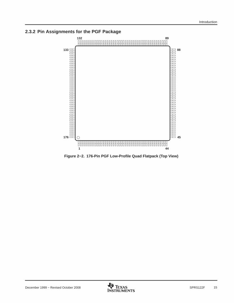
2.3.2 Pin Assignments for the PGF Package89
88
45
44
132
133
176
1
Figure 2−2. 176-Pin PGF Low-Profile Quad Flatpack (Top View)

Introduction
16 December 1999 − Revised October 2008SPRS122F
Table 2−2. Pin Assignments for TMS320VC5441PGF (176-Pin LQFP Package) † PIN NO. SIGNAL NAME PIN NO. SIGNAL NAME PIN NO. SIGNAL NAME PIN NO. SIGNAL NAME
1 HA[0]/HCNTL0 2 HA[1]/HCNTL1 3 HA[2]/A_HINT 4 HA[3]/B_HINT
5 HA[4]/C_HINT 6 VSS 7 VSS 8 B_RS
9 B_NMI 10 B_INT 11 CLKMD 12 TDI
13 TESTB 14 DVDD 15 HAS 16 HCS
17 VSS 18 VSSA 19 CLKIN 20 HRDY
21 VCCA 22 CVDD 23 CVDD 24 EMU0
25 BCLKR2 26 BCLKX2 27 VSS 28 BFSR2
29 BFSX2 30 CLKOUT 31 DVDD 32 BDR2
33 BDX2 34 VSS 35 A_RS 36 A_NMI
37 A_INT 38 TDO 39 HA[5]/D_HINT 40 HA[6]
41 HA[7] 42 HA[8] 43 VSS 44 HA[9]
45 A_BFSX0 46 DVDD 47 A_GPIO1/A_BIO 48 A_BFSR0
49 A_GPIO3/A_TOUT 50 VSS 51 A_GPIO0/A_XF 52 A_BDR0
53 CVDD 54 A_BDX0 55 CVDD 56 CVDD57 CVDD 58 A_GPIO2/A_WTOUT 59 A_BCLKR0 60 A_BCLKX0
61 VSS 62 HD[8] 63 HD[9] 64 DVDD65 DVDD 66 HD[10] 67 HD[11] 68 HD[12]
69 HD[13] 70 VSS 71 HD[14] 72 HD[15]
73 C_BCLKX0 74 CVDD 75 CVDD 76 CVDD77 C_BDR0 78 CVDD 79 C_GPIO3/C_TOUT 80 C_BCLKR0
81 C_GPIO0/C_XF 82 VSS 83 C_BDX0 84 C_GPIO1/C_BIO
85 C_GPIO2/C_WTOUT 86 DVDD 87 DVDD 88 C_BFSR0
89 C_BFSX0 90 HA[10] 91 HA[11] 92 HA[12]
93 HA[13] 94 VSS 95 HA[14] 96 TESTC
97 C_INT 98 HDS1 99 C_RS 100 BDX1
101 BDR1 102 BCLKR1 103 DVDD 104 BFSR1
105 BFSX1 106 VSS 107 BCLKX1 108 HMODE
109 CVDD 110 HR/W 111 RESET 112 C_NMI
113 HDS2 114 VSS 115 HPI_SEL1 116 HPI_SEL2
117 EMU1/OFF 118 DVDD 119 TCK 120 TMS
121 TRST 122 TESTD 123 D_INT 124 D_NMI
125 D_RS 126 VSS 127 VSS 128 HA[15]
129 HA[16] 130 HA[17] 131 HA[18] 132 D_BFSR0
133 D_BFSX0 134 DVDD 135 DVDD 136 D_GPIO2/D_WTOUT
137 D_BDX0 138 D_BCLKR0 139 VSS 140 D_BCLKX0
141 D_GPIO0/D_XF 142 CVDD 143 D_BDR0 144 CVDD145 CVDD 146 CVDD 147 D_GPIO1/D_BIO 148 D_GPIO3/D_TOUT
149 HD[0] 150 VSS 151 HD[1] 152 HD[2]
153 DVDD 154 HD[3] 155 HD[4] 156 HD[5]
157 HD[6] 158 VSS 159 HD[7] 160 B_BCLKR0
161 B_BCLKX0 162 CVDD 163 CVDD 164 CVDD165 B_BDR0 166 CVDD 167 B_BDX0 168 B_GPIO3/B_TOUT
169 B_GPIO0/B_XF 170 VSS 171 B_BFSR0 172 B_GPIO2/B_WTOUT
173 B_GPIO1/B_BIO 174 DVDD 175 DVDD 176 B_BFSX0
† Cells highlighted in gray indicate pins that perform a multiplexed function.

Introduction
17December 1999 − Revised October 2008 SPRS122F
2.4 Signal Descriptions
Table 2−3 lists all the signals, grouped by function. See Section 2.3 for the exact pin locations based on the
package type. Pin functions highlighted in gray are secondary (multiplexed) functions.
Table 2−3. Signal Descriptions
NAME TYPE† DESCRIPTION
HOST-PORT INTERFACE SIGNALS
HA18 (MSB)HA17HA16HA15HA14HA13HA12HA11HA10HA9HA8HA7HA6
I‡
HPI address pins when HPI is in nonmultiplexed mode. HA18 is used to facilitate program (shared) memory and data(local) memory selection.
The pins include bus holders to reduce power dissipation caused by floating, unused pins. The bus holders alsoeliminate the need for external pullup resistors on unused pins. When the address bus is not being driven by theexternal host, the bus holders keep address pins at the last driven logic level. The address bus keepers are disabledat global reset or subsystem A reset, and can be enabled/disabled via the BHA bit of the BSCR register in subsystem A.
SECONDARY
HA5HA4HA3HA2
D_HINTC_HINTB_HINTA_HINT
O/Z§
HA1HA0 (LSB)
HCNTL1HCNTL0
I
HD15 (MSB)HD14HD13HD12HD11HD10HD9HD8HD7HD6HD5 HD4HD3HD2HD1HD0 (LSB)
I/O/Z‡§
Parallel bidirectional data bus. These pins are the HPI data bus.
The pins include bus holders to reduce power dissipation caused by floating, unused pins. The bus holders alsoeliminate the need for external pullup resistors on unused pins. When the data bus is not being driven by the 5441,the bus holders keep data pins at the last driven logic level. The data bus keepers are disabled at global reset orsubsystem A reset, and can be enabled/disabled via the BHD bit of the BSCR register in subsystem A.
† I = Input, O = Output, S = Supply, Z = High Impedance‡ This pin has an internal bus holder controlled by way of the BSCR register in TMS320C54x cLEAD core of DSP subsystem A.§ This pin is placed in high-impedance when the EMU1/OFF pin operates as OFF and when EMU1/OFF = 0, this case is exclusively for testing
and emulation purposes.¶ This pin has an internal pullup resistor.# These pins are Schmitt triggered inputs.|| This pin is used by Texas Instruments for device testing and should be left unconnected.This pin has an internal pulldown resistor.Although this pin includes an internal pulldown resistor, a 470-Ω external pulldown is required. If the TRST pin is connected to multiple DSPs,
a buffer is recommended to ensure the VIL and VIH specifications are met.NOTE: Pins highlighted in grey indicate the multiplexed function of the pin.

Introduction
18 December 1999 − Revised October 2008SPRS122F
Table 2−3. Signal Descriptions (Continued)
NAME DESCRIPTIONTYPE†
HOST-PORT INTERFACE SIGNALS (CONTINUED)
HMODE¶ I
HPI mode select. When this pin is low, it selects the HPI multiplexed address/data mode. The multiplexed address/datamode allows hosts with multiplexed address/data lines access to the HPI registers HPIA, HPIC, and HPID.Host-to-DSP and DSP-to-host interrupts are supported in this mode.
When HMODE is high, it selects the HPI nonmultiplexed mode. HPI nonmultiplexed mode allows hosts with separateaddress/data buses to access the HPI address range by way of the 19-bit address bus and the HPI data (HPID) registervia the 16-bit data bus. Host-to-DSP and DSP-to-host interrupts are not supported in this mode.
HAS¶# IHPI address latch enable (ALE) or address strobe input. Hosts with multiplexed address and data pins require HASto latch the address in the HPIA register. This signal is used only in HPI multiplexed address/data mode (HMODE = 0).
HRDY O/Z§ HPI data ready output. The ready output informs the host when the HPI is ready for the next transfer. While driving,it is in output state and while not driving, it is in high-Z state.
HR/W I HPI read/write strobe. This signal is used by the host to control the direction of an HPI transfer.
HDS1¶#¶# I HPI data strobes. Driven by the host read and write strobes to control HPI transfers.
HDS1¶#
HDS2¶# I HPI data strobes. Driven by the host read and write strobes to control HPI transfers.
HCS¶# I HPI chip select. Must be active during HPI transfers and can remain active between concurrent transfers.
PRIMARY
D_HINTC_HINTB_HINTA_HINT
O/Z§HA5HA4HA3HA2
I
Host interrupt pins. HPI can interrupt the host by asserting this low. The host can clear thisinterrupt by writing a “1” to the HINT bit of the HPIC register. Only supported in HPImultiplexed address/data mode (HMODE pin low)
HCNTL1HCNTL0
IHA1HA0
IHPI control pins. These pins select a host access to the HPIA, HPIC, and HPID registers.Only supported in HPI multiplexed address/data mode (HMODE pin low)
HPI_SEL1I Subsystem HPI module select
HPI_SEL1HPI_SEL2
I Subsystem HPI module select
MULTICHANNEL BUFFERED SERIAL PORTS 0, 1, AND 2 SIGNALS
A_BCLKR0#
B_BCLKR0#
C_BCLKR0#
D_BCLKR0#
I/O/Z§
Receive clocks. x_BCLKR0 serve as the serial shift clocks for the buffered serial-port receiver. Input from an externalclock source for clocking data into the McBSP. When not being used as clocks, these pins can be used asgeneral-purpose I/Os by setting RIOEN = 1.
x_BCLKR0 can be configured as outputs by way of the CLKRM bit in the PCR register.
A_BCLKX0#
B_BCLKX0#
C_BCLKX0#
D_BCLKX0#
I/O/Z§Transmit clocks. Clock signals used to clock data from the transmit register. These pins can also be configured asinputs by setting CLKXM = 0 in the PCR register. x_BCLKX0 can be sampled as inputs by way of the IN1 bit in theSPC register. When not being used as clocks, these pins can be used as general-purpose I/Os by setting XIOEN = 1.
A_BDR0B_BDR0C_BDR0D_BDR0
IBuffered serial data receive (input) pins. When not being used as data-receive pins, these pins can be used asgeneral-purpose I/Os by setting RIOEN = 1.
† I = Input, O = Output, S = Supply, Z = High Impedance‡ This pin has an internal bus holder controlled by way of the BSCR register in TMS320C54x cLEAD core of DSP subsystem A.§ This pin is placed in high-impedance when the EMU1/OFF pin operates as OFF and when EMU1/OFF = 0, this case is exclusively for testing
and emulation purposes.¶ This pin has an internal pullup resistor.# These pins are Schmitt triggered inputs.|| This pin is used by Texas Instruments for device testing and should be left unconnected.This pin has an internal pulldown resistor.Although this pin includes an internal pulldown resistor, a 470-Ω external pulldown is required. If the TRST pin is connected to multiple DSPs,
a buffer is recommended to ensure the VIL and VIH specifications are met.NOTE: Pins highlighted in grey indicate the multiplexed function of the pin.

Introduction
19December 1999 − Revised October 2008 SPRS122F
Table 2−3. Signal Descriptions (Continued)
NAME DESCRIPTIONTYPE†
MULTICHANNEL BUFFERED SERIAL PORTS 0, 1, AND 2 SIGNALS (CONTINUED)
A_BDX0B_BDX0C_BDX0D_BDX0
O/Z§ Buffered serial-port transmit (output) pins. When not being used as data-transmit pins, x_BDX0 can be used asgeneral-purpose I/Os by setting XIOEN = 1.
A_BFSR0B_BFSR0C_BFSR0D_BFSR0
I/O/Z§Frame synchronization pins for buffered serial-port input data. The x_BFSR0 pulse initiates the receive-data processover x_BDR0. When not being used as data-receive synchronization pins, these pins can be used as general-purposeI/Os by setting RIOEN = 1.
A_BFSX0B_BFSX0C_BFSX0D_BFSX0
I/O/Z§
Buffered serial-port frame synchronization pins for transmitting data. The x_BFSX0 pulse initiates the transmit-dataprocess over the x_BDX0 pin. If x_RS is asserted when x_BFSX0 is configured as output, then x_BFSX0 is turnedinto input mode by the reset operation. When not being used as data-transmit synchronization pins, these pins canbe used as general-purpose I/Os by setting XIOEN = 1.
BCLKR1# Receive clock, multiplexed McBSP1
BCLKX1# I Transmit clock, multiplexed McBSP1
BDR1
I
Receive data, multiplexed McBSP1
BDX1 O/Z§ Transmit data, multiplexed McBSP1
BFSR1I
Receive frame sync, multiplexed McBSP1
BFSX1I
Transmit frame sync, multiplexed McBSP1
BCLKR2# Receive clock, multiplexed McBSP2
BCLKX2# I Transmit clock, multiplexed McBSP2
BDR2
I
Receive data, multiplexed McBSP2
BDX2 O/Z§ Transmit data, multiplexed McBSP2
BFSR2I
Receive frame sync, multiplexed McBSP2
BFSX2I
Transmit frame sync, multiplexed McBSP2
CLOCKING SIGNALS
CLKOUT O/Z§
Master clock output signal. CLKOUT cycles at the machine-cycle rate of the CPU. The internal machine cycle isbounded by the falling edges of this signal. The CLKOUT pin can be turned off by writing a “1” to the CLKOUT bit ofthe PMST register.
Multiplexed as shown below based on the selection bits in the GPIO registerCLKOUT O/Z§
GPIO[7] GPIO[6]
A_CLKOUT 0 0 (default)
B_CLKOUT|| 0 1
C_CLKOUT|| 1 0
D_CLKOUT|| 1 1
CLKIN# I Input clock to the device. CLKIN connects to a PLL.
CLKMD# I Clock mode configuration pin at reset. When CLKMD = 0, bypasses PLL; when CLKMD = 1, CLKINx2† I = Input, O = Output, S = Supply, Z = High Impedance‡ This pin has an internal bus holder controlled by way of the BSCR register in TMS320C54x cLEAD core of DSP subsystem A.§ This pin is placed in high-impedance when the EMU1/OFF pin operates as OFF and when EMU1/OFF = 0, this case is exclusively for testing
and emulation purposes.¶ This pin has an internal pullup resistor.# These pins are Schmitt triggered inputs.|| This pin is used by Texas Instruments for device testing and should be left unconnected.This pin has an internal pulldown resistor.Although this pin includes an internal pulldown resistor, a 470-Ω external pulldown is required. If the TRST pin is connected to multiple DSPs,
a buffer is recommended to ensure the VIL and VIH specifications are met.NOTE: Pins highlighted in grey indicate the multiplexed function of the pin.

Introduction
20 December 1999 − Revised October 2008SPRS122F
Table 2−3. Signal Descriptions (Continued)
NAME DESCRIPTIONTYPE†
GENERAL-PURPOSE I/O PINS
A_GPIO0/A_XF
Subsystem A GPIO0/Subsystem A external flag output
These pins act according to theB_GPIO0/B_XF
I/O/Z§
Subsystem B GPIO0/Subsystem B external flag output
These pins act according to thegeneral-purpose I/O register. Thex_XF bit must be set to “1” to drive the
C_GPIO0/C_XF
I/O/Z§Subsystem C GPIO0/Subsystem C external flag output
x_XF bit must be set to “1” to drive thex_XF output on the pin. If x_XF=0,then these pins are general-purposeI/Os.
D_GPIO0/D_XF
Subsystem D GPIO0/Subsystem D external flag output
I/Os.
A_GPIO1/A_BIO
Subsystem A GPIO1/Subsystem A branch control input
These pins act according to theB_GPIO1/B_BIO
I/O/Z§
Subsystem B GPIO1/Subsystem B branch control input
These pins act according to thegeneral-purpose I/O register. Thex_BIO bit must be set to “1” to drive the
C_GPIO1/C_BIO
I/O/Z§Subsystem C GPIO1/Subsystem C branch control input
x_BIO bit must be set to “1” to drive thex_BIO input into the device. Ifx_BIO=0, then these pins aregeneral-purpose I/Os.
General-purpose I/O pins (software-programmable I/O signal). Values
D_GPIO1/D_BIO
Subsystem D GPIO1/Subsystem D branch control input
general-purpose I/Os. programmable I/O signal). Valuescan be latched (output) by writing intothe GPIO register. The states of GPIO
A_GPIO2/A_WTOUT
Subsystem A GPIO2/Subsystem A watchdog timer output
The watchdog enable (WDEN) bit in
the GPIO register. The states of GPIOpins (inputs) can be determined byreading the GPIO register. The GPIOdirection is also programmable by
B_GPIO2/B_WTOUT
I/O/Z§
Subsystem B GPIO2/Subsystem B watchdog timer output
The watchdog enable (WDEN) bit inthe watchdog timer register(WDTSCR) is used to multiplex the
direction is also programmable byway of the DIRn field in the register.
C_GPIO2/C_WTOUT
I/O/Z§Subsystem C GPIO2/Subsystem C watchdog timer output
(WDTSCR) is used to multiplex thewatchdog timer output and GPIO2. IfWDEN=0, then these pins aregeneral-purpose I/Os.
D_GPIO2/D_WTOUT
Subsystem D GPIO2/Subsystem D watchdog timer output
general-purpose I/Os.
A_GPIO3/A_TOUT
Subsystem A GPIO3/Subsystem A timer output
These pins act according to theB_GPIO3/B_TOUT
I/O/Z§
Subsystem B GPIO3/Subsystem B timer output
These pins act according to thegeneral-purpose I/O register. TheX_TOUT bit must be set to “1” to drive
C_GPIO3/C_TOUT
I/O/Z§Subsystem C GPIO3/Subsystem C timer output
X_TOUT bit must be set to “1” to drivethe timer output on the pin. IfX_TOUT=0, then these pins aregeneral-purpose I/Os.
D_GPIO3/D_TOUT
Subsystem D GPIO3/Subsystem D timer output
general-purpose I/Os.
† I = Input, O = Output, S = Supply, Z = High Impedance‡ This pin has an internal bus holder controlled by way of the BSCR register in TMS320C54x cLEAD core of DSP subsystem A.§ This pin is placed in high-impedance when the EMU1/OFF pin operates as OFF and when EMU1/OFF = 0, this case is exclusively for testing
and emulation purposes.¶ This pin has an internal pullup resistor.# These pins are Schmitt triggered inputs.|| This pin is used by Texas Instruments for device testing and should be left unconnected.This pin has an internal pulldown resistor.Although this pin includes an internal pulldown resistor, a 470-Ω external pulldown is required. If the TRST pin is connected to multiple DSPs,
a buffer is recommended to ensure the VIL and VIH specifications are met.NOTE: Pins highlighted in grey indicate the multiplexed function of the pin.

Introduction
21December 1999 − Revised October 2008 SPRS122F
Table 2−3. Signal Descriptions (Continued)
NAME DESCRIPTIONTYPE†
INITIALIZATION, INTERRUPT, AND RESET OPERATIONS
A_INT¶#
B_INT¶#
C_INT¶#
D_INT¶#
IExternal user interrupts. A_INT−D_INT are prioritized and are maskable by the interrupt mask register (IMR) and theinterrupt mode bit. The status of these pins can be polled and reset by way of the interrupt flag register (IFR).
A_NMI¶#
B_NMI¶#
C_NMI¶#
D_NMI¶#
INonmaskable interrupts. x_NMI is an external interrupt that cannot be masked by way of the INTM bit or the IMR. Whenx_NMI is activated, the processor traps to the appropriate vector location.
A_RS#
B_RS#
C_RS#
D_RS#
IReset. x_RS causes the digital signal processor (DSP) to terminate execution and causes a reinitialization of the CPUand peripherals. When x_RS is brought to a high level, execution begins at location 0FF80h of program memory. x_RSaffects various registers and status bits.
RESET# I Global/HPI reset. This signal resets the four subsystems and the HPI.
SUPPLY PINS
VCCA Dedicated power supply that powers the PLL. VDD = 1.6 V
CVDD Dedicated power supply that powers the core CPUs. CVDD = 1.6 V
DVDD SDedicated power supply that powers the I/O pins. DVDD = 3.3 V
VSSS
Digital ground. Dedicated ground plane for the device.
VSSAAnalog ground. Dedicated ground for the PLL. VSSA can be connected to VSS if digital and analog grounds are notseparated.
EMULATION/TEST PINS
TESTB||
TESTC||
TESTD||No connection
TCK¶# IStandard test clock. This is normally a free-running clock signal with a 50% duty cycle. Changes on the test accessport (TAP) input signals TMS and TDI are clocked into the TAP controller, instruction register, or selected test-dataregister on the rising edge of TCK. Changes at the TAP output signal (TDO) occur on the falling edge of TCK.
TDI¶ ITest data input. Pin with an internal pullup device. TDI is clocked into the selected register (instruction or data) on arising edge of TCK.
TDO O/Z§ Test data pin. The contents of the selected register is shifted out of TDO on the falling edge of TCK. TDO is inhigh-impedance state except when the scanning of data is in progress.
TMS¶ ITest mode select. Pin with internal pullup device. This serial control input is clocked into the TAP controller on the risingedge of TCK.
TRST IIEEE standard 1149.1 test reset. TRST, when high, gives the IEEE standard 1149.1 scan system control of theoperations of the device. If TRST is driven low, the device operates in its functional mode, and the IEEEstandard 1149.1 signals are ignored. Pin with internal pulldown device.
EMU0 I/O/ZEmulator interrupt 0 pin. When TRST is driven low, EMU0 must be high for the activation of the EMU1/OFF condition.When TRST is driven high, EMU0 is used as an interrupt to or from the emulator system and is defined as I/O.
† I = Input, O = Output, S = Supply, Z = High Impedance‡ This pin has an internal bus holder controlled by way of the BSCR register in TMS320C54x cLEAD core of DSP subsystem A.§ This pin is placed in high-impedance when the EMU1/OFF pin operates as OFF and when EMU1/OFF = 0, this case is exclusively for testing
and emulation purposes.¶ This pin has an internal pullup resistor.# These pins are Schmitt triggered inputs.|| This pin is used by Texas Instruments for device testing and should be left unconnected.This pin has an internal pulldown resistor.Although this pin includes an internal pulldown resistor, a 470-Ω external pulldown is required. If the TRST pin is connected to multiple DSPs,
a buffer is recommended to ensure the VIL and VIH specifications are met.NOTE: Pins highlighted in grey indicate the multiplexed function of the pin.

Introduction
22 December 1999 − Revised October 2008SPRS122F
Table 2−3. Signal Descriptions (Continued)
NAME DESCRIPTIONTYPE†
EMULATION/TEST PINS (CONTINUED)
EMU1/OFF I/O/Z
Emulator interrupt 1 pin. When TRST is driven high, EMU1/OFF is used as an interrupt to or from the emulator systemand is defined as I/O. When TRST transitions from high to low, then EMU1 operates as OFF. EMU/OFF = 0 puts alloutput drivers into the high-impedance state.
Note that OFF is used exclusively for testing and emulation purposes (and not for multiprocessing applications).Therefore, for the OFF condition, the following conditions apply:
TRST = 0, EMU0 = 1, EMU1 = 0
† I = Input, O = Output, S = Supply, Z = High Impedance‡ This pin has an internal bus holder controlled by way of the BSCR register in TMS320C54x cLEAD core of DSP subsystem A.§ This pin is placed in high-impedance when the EMU1/OFF pin operates as OFF and when EMU1/OFF = 0, this case is exclusively for testing
and emulation purposes.¶ This pin has an internal pullup resistor.# These pins are Schmitt triggered inputs.|| This pin is used by Texas Instruments for device testing and should be left unconnected.This pin has an internal pulldown resistor.Although this pin includes an internal pulldown resistor, a 470-Ω external pulldown is required. If the TRST pin is connected to multiple DSPs,
a buffer is recommended to ensure the VIL and VIH specifications are met.NOTE: Pins highlighted in grey indicate the multiplexed function of the pin.

Functional Overview
23December 1999 − Revised October 2008 SPRS122F
3 Functional OverviewThe functional overview in this section is based on the overall system block diagram in Figure 3−1 and thetypical subsystem block diagram in Figure 3−2.
GPIO
McBSP0McBSP1McBSP2
DSPSubsystem ADSP ID: 0000
HPI
XA
PLL
Shared P Bus
McBSP2McBSP1McBSP0
GPIO
HPI
DSPSubsystem CDSP ID: 0010 Shared P Bus
SA1
DSPSubsystem BDSP ID: 0001
GPIO
McBSP0McBSP1McBSP2
HPI
DSP ID: 0011Subsystem D
DSP
GPIO
McBSP0McBSP1McBSP2
McBSP1
McBSP2
HPI
SA2
Figure 3−1. Overall Functional Block Diagram
P. C. D. E. Busses and Control Signals
P B
us
C B
us
D B
us
E B
us
TMS320C54x cLEAD(Core)
64K-WordData DARAM
M Bus
32K-Word Program/Data
DARAM
M Bus
3 × McBSP
M B
us
Shared P Bus
M BusTimer DMA
WDTimer
GPIOHPI
C B
us
D B
us
E B
us
P B
us
C B
us
D B
us
E B
us
P B
us
DSP Subsystem
HPI Bus
M Bus
64K-WordProgram DARAM
Figure 3−2. Typical Subsystem Functional Block Diagram

Functional Overview
24 December 1999 − Revised October 2008SPRS122F
3.1 Memory
Each 5441 DSP subsystem maintains the peripheral register memory map and interrupt location/priorities ofthe standard 5421. Each individual subsystem CPU memory map is illustrated in Figure 3−3 throughFigure 3−6.
The arbitration and access for local program/data memory and local data memory is based on a 16K-wordblock size. The arbitration and access for all the shared memory is based on a 32K-word block size.
3.1.1 Memory Maps
Figure 3−3 through Figure 3−6 illustrate the CPU memory maps for subsystem A through subsystem D.Figure 3−7 provides a detailed memory map of the local data memory relative to CPU subsystems A, B, C,and D.
Page 0
Data Memory
Page 1
8000h
Page 2
FFFFh
Page 3
0000h
"
Page 0
Data Memory
Page 1
Program Memory
Page 2 Page 3
0000h
8000h
FFFFh
: reserved
Program Memory
Memory Map with OVLY = 1
" " ""
"#$"#% "#& "#'
ÒÒÒÒÒÒÒÒ
"#$" "#$ "#$ "#$
"#% "#& "#'
ÒÒÒÒ
Memory Map with OVLY = 0
"%
"&
"%
"&
NOTES: A. MPDA: local program/data memory in subsystem AB. MDA: local data memory in subsystem A. MDA is controlled by the data memory map register (DMMR).
DMMR=0, MDA0 is mapped in 8000h − FFFFh.DMMR=1, MDA1 is mapped in 8000h − FFFFh.
C. MPAB: shared program memory in subsystems A and B
Figure 3−3. Subsystem A CPU Memory Map

Functional Overview
25December 1999 − Revised October 2008 SPRS122F
Page 0
Data Memory
Page 1
Program Memory
Page 2 Page 3
0000h
8000h
FFFFh
"# "#
Page 0
Data Memory
Page 1
Program Memory
Page 2
ÒÒÒÒÒÒÒÒ
Page 3
"#$
0000h
8000h
FFFFh
"#
ÕÕ: reserved
"#$"#% "#& "#'
"#% "#& "#'
Memory Map with OVLY = 1
Memory Map with OVLY = 0
"# "# "#
"#$ "#$ "#$
"#%
"#&
"#%
"#&
NOTES: A. MPDB: local program/data memory in subsystem BB. MDB: local data memory in subsystem B. MDB is controlled by the data memory map register (DMMR).
DMMR=0, MDB0 is mapped in 8000h − FFFFh.DMMR=1, MDB1 is mapped in 8000h − FFFFh.
C. MPAB: shared program memory in subsystems A and B
Figure 3−4. Subsystem B CPU Memory Map

Functional Overview
26 December 1999 − Revised October 2008SPRS122F
Page 0
Data Memory
Page 1
Program Memory
Page 2 Page 3
0000h
8000h
FFFFh
" "
Page 0
Data Memory
Page 1
Program Memory
Page 2 Page 3
"$
0000h
8000h
FFFFh
"
: reserved
"$"% "& "'
"% "& "'
Memory Map with OVLY = 0
Memory Map with OVLY = 1
" " "
"$ "$ "$
ÒÒÒÒÒÒÒÒ
ÒÒ
"%
"&
"%
"&
NOTES: A. MPDC: local program/data memory in subsystem CB. MDC: local data memory in subsystem C. MDC is controlled by the data memory map register (DMMR).
DMMR=0, MDC0 is mapped in 8000h − FFFFh.DMMR=1, MDC1 is mapped in 8000h − FFFFh.
C. MPCD: shared program memory in subsystems C and D
Figure 3−5. Subsystem C CPU Memory Map

Functional Overview
27December 1999 − Revised October 2008 SPRS122F
Page 0
Data Memory
Page 1
Program Memory
Page 2 Page 3
0000h
8000h
FFFFh
" "
Page 0
Data Memory
Page 1
Program Memory
Page 2
ÒÒÒÒÒÒÒÒ
Page 3
"$
0000h
8000h
FFFFh
MPDD
ÕÕÕÕ
reserved
"$"% "& "'
"% "& "'
" " "
"$ "$ "$
Memory Map with OVLY = 1
Memory Map with OVLY = 0
"%
"&
"%
"&
NOTES: A. MPDD: local program/data memory in subsystem DB. MDD: local data memory in subsystem D. MDD is controlled by the data memory map register (DMMR).
DMMR=0, MDD0 is mapped in 8000h − FFFFh.DMMR=1, MDD1 is mapped in 8000h − FFFFh.
C. MPCD: shared program memory in subsystems C and D
Figure 3−6. Subsystem D CPU Memory Map
Figure 3−7 shows the CPU data memory map. The lower 32K-word data memory location in all pages is theoverlay area. Program memory has overlay area over the lower 32K words on all pages as well.
The overlay areas refer to:
1. When OVLY = 1, the lower 32K words of data space are mapped to the lower 32K words of all programpages in the memory map.
2. When OVLY = 0, the lower 32K words of data space are mapped only to the lower 32K words of data spaceand the lower 32K words of program page 3 are mapped to the lower 32K words of all program pages.

Functional Overview
28 December 1999 − Revised October 2008SPRS122F
Memory-Mapped
Registers
00 0000
00 005F00 0060
00 7FFF00 8000
00 FFFF
Hex
Data Memory
16K Words
16K Words
16K Words
16K Words
00 3FFF00 4000
00 BFFF00 C000
DARAM0
DARAM1
DARAM2
(DMMR=0)
DARAM4
DARAM3
DARAM5
(DMMR=0)
(DMMR=1)
(DMMR=1)
NOTE: The upper part of data memory is controlled by the Data Memory Map Register (DMMR).1. DMMR=0, DARAM2 and DARAM3 are mapped in 8000h − FFFFh.2. DMMR=1, DARAM4 and DARAM5 are mapped in 8000h − FFFFh.
Figure 3−7. Detailed Memory Map of Local Data Memory Relative to CPU Subsystems A, B, C, and D
3.1.2 On-Chip Dual-Access RAM (DARAM)
Each 5441 subsystem has 96K 16-bit words of on-chip DARAM (six blocks of 16K words). Each of theseDARAM blocks can be accessed twice per machine cycle. This memory is intended primarily to store datavalues; however, it can be used to store program as well. At reset, the DARAM is mapped into data memoryspace (OVLY=0). The lower part of DARAM (0000h−8000h) can be mapped into program/data memory spaceby setting the OVLY bit in the processor-mode status (PMST) register of the TMS320C54x cLEAD CPU ineach DSP subsystem.
3.1.3 On-Chip Two-Way Shared RAM
There are 128K 16-bit words of on-chip RAM (four blocks of 32K words) that are shared between subsystemsA and B. There are 128K 16-bit words of on-chip RAM (four blocks of 32K words) that are shared betweensubsystems C and D. This memory is intended to store program only. Both subsystems are able to make oneinstruction fetch from any location in the two-way shared memory each cycle simultaneously. No subsystemCPU can write to the shared memory as only the DMA can write to shared memory.
If any of the CPU program fetches are requested at the same time as an M-bus transfer request, the CPU isstalled until all M bus transfers are completed. In other words, any read or write requested by the M bus (drivenby DMA controller or HPI) has priority over the CPUs’ (A, B, C, and D) program fetches. The M-bus reads orwrites always take two cycles to complete.
Functional Overview
29December 1999 − Revised October 2008 SPRS122F
3.1.4 Extended Data Memory
The data memory space of each 5441 subsystem addresses 128K 16-bit words. There are two pages of datamemory location with each page consisting of 64K words. The 5441 device uses a data memory map register(DMMR) to facilitate extended data memory access. The DMMR is a peripheral memory-mapped register. Thecontents of the DMMR register, once being written with an extended data number by the DSP CPU, will beassociated with the address decoding for all the data memory CPU accesses.
3.1.5 Extended Program Memory
The 5441 device uses a paged extended memory scheme in program space to allow access to 256K 16-bitwords. This extended program memory (each subsystem) is organized into four pages (0−3), pages 0−3 aretwo-way shared memory. Each page is 64K words in length. The program counter extension register (XPC)defines the program page selection. To implement the extended program memory scheme, the 5441 deviceincludes the following feature:
• Two C54x instructions allow each subsystem CPU access to the on-chip program memory.
− READA − Read program memory addressed by accumulator A and store in data memory− WRITA − Write data to program memory addressed by accumulator A
(Writes not allowed for CPUs to shared program memory)
3.1.6 Program Memory
The program memory is accessible on multiple pages, depending on the XPC value. Within these pages,memory is accessible depending on the address range.
• Access in the lower 32K words of each page is dependent on the state of OVLY.
− OVLY = 0 − Program memory is accessed from program memory page 3 for all values of XPC.− OVLY = 1 − Program memory is accessed from local data/program DARAM for all values of XPC.
• Access in the upper 32K words of each page is dependent on the state of OVLY.
− OVLY = 0 − All pages of program memory except page 3 (which is reserved) are accessible for allvalues of XPC.
− OVLY = 1 − All pages of program memory are accessible for all values of XPC.
3.1.7 Data Memory
Accesses on extended data spaces are dependent on the value of the data memory map register (DMMR).Within the page, memory is accessible depending on the address range.
• Access in the lower 32K words
− Data memory is accessed from local data/program DARAM for all values of DMMR.
• Access in the upper 32K words
− Which data memory block is accessed depends on the value of DMMR.
− There are four 16K-word DARAM blocks for the upper addresses (8000h − FFFFh)DMMR=0: DARAM2 and DARAM3 are mapped to the upper addressesDMMR=1: DARAM4 and DARAM5 are mapped to the upper addresses
3.1.8 I/O Memory
The 5441 does not support I/O memory accesses.
C54x is a trademark of Texas Instruments.

Functional Overview
30 December 1999 − Revised October 2008SPRS122F
3.1.9 Multicore Reset Signals
The 5441 device includes five reset signals: A_RS, B_RS, C_RS, D_RS, and RESET. The A_RS, B_RS,C_RS, and D_RS local reset signals function as the CPU reset signal for subsystem A, B, C, and D,respectively. The RESET services as a global reset for the whole device.
The global reset (RESET) is a superset of local resets A_RS, B_RS, C_RS, and D_RS. The assertion ofRESET triggers all the local resets; however, none of the local resets triggers the global reset. The local resetsignals reset the state of the CPU registers and CPU memory-mapped peripheral registers, and upon release,initiate the reset function. The global reset, RESET, resets the on-chip PLL and clears the watchdog timer flag(WDFLAG) bit. The local reset signals are not able to reset the PLL or clear the WDFLAG.
The global reset (RESET) and local resets (x_RS) clears the program counter extension register (XPC) to zerowhile the RESET instruction does not affect the XPC.
3.1.10 Device Bootload
The 5441 device supports an HPI boot sequence, which is used to download code while the DSP is in reset.The external master holds the device in reset while it loads code to the on-chip memory of each subsystem,subsystem selection is made by HPI_SEL1 and HPI_SEL2 signals. The host can release the 5441 from resetby using either of the following methods.
• If the x_RS (x = A, B, C, or D for subsystem A, B, C, or D, respectively) pins are held low while RESETtransitions from low to high, the reset of each subsystem will be controlled by the x_RS pins. When thehost has finished downloading code, it can drive x_RS high to release the cores from reset.
• If the x_RS pins are held high while RESET transitions from low to high, the subsystems will stay in resetuntil an HPI data write to address 0x2F occurs. This means the host can download code to subsystemx and then release core x from reset by writing any data to core x’s address 0x2F via the HPI. The hostcan then repeat the sequence for other cores. This mode allows the host to control 5441 reset withoutadditional hardware.
3.2 On-Chip Peripherals
All the C54x devices have the same CPU structure; however, they have different on-chip peripheralsconnected to their CPUs. The on-chip peripheral options provided are:
• DMA controller• 16-bit host-port interface I/O ports• Multichannel buffered serial ports (McBSPs)• A hardware timer• A hardware watchdog timer• A software-programmable clock generator using a phase-locked loop (PLL)• General-purpose I/O
3.2.1 Direct Memory Access (DMA) Controller
The 5441 includes four 6-channel direct memory access (DMA) controllers for performing data transfersindependent of the CPU, one controller for each subsystem. The primary function of the 5441 DMA controlleris to provide code overlays and to manage data transfers between on-chip memory, the peripherals, andoff-chip host.
In the background of CPU operation, the 5441 DMA allows movement of data between internal program/datamemory and internal peripherals, such as the McBSPs and the HPI. Each subsystem has its own independentDMA with six programmable channels, which allows for six different contexts for DMA operation. The HPI hasa dedicated auxiliary DMA channel. The remapped areas represent address aliasing for DMA accesses withineach subsystem. Figure 3−8 through Figure 3−11 illustrate the local DMA memory map of each subsystem.

Functional Overview
31December 1999 − Revised October 2008 SPRS122F
Page 0
Data Memory
Page 1
Program Memory
Page 2 Page 3
0000h
8000h
FFFFh
Page 0
MPDA
Page 1
Reserved
ÇÇÇÇÒÒÒÒ
: Remapped areasMcBSP DXR/DRR MMRegs only
0020h
0060hMPDA MPDA MPDA MPDA MPDA
MPAB0 MPAB1MDA0 MDA1 MPAB0 MPAB1
ÇÇÇÇ
ÒÒÒÒ
NOTES: A. MPDA: local program/data memory in subsystem AB. MDA: local data memory in subsystem AC. MPAB: two-way shared program memory in subsystems A and B
Figure 3−8. Subsystem A Local DMA Memory Map
Page 0
Data Memory
Page 1
Program Memory
Page 2 Page 3
0000h
8000h
FFFFh
Page 0
"#
"#%
Page 1
"#&
Ç Reserved
ÇÇÇÇÒÒÒÒ
ÕÕ McBSP DXR/DRR MMRegs only
"# "# "# "# "#
"#' "#$
: Remapped areas
0020h
0060h
"#' "#$
NOTES: A. MPDB: local program/data memory in subsystem BB. MDB: local data memory in subsystem BC. MPAB: two-way shared program memory in subsystems A and B
Figure 3−9. Subsystem B Local DMA Memory Map

Functional Overview
32 December 1999 − Revised October 2008SPRS122F
Page 0
Data Memory
Page 1
Program Memory
"% "&
Page 2 Page 3
0000h
8000h
FFFFh
Page 0
"
"%
Page 1
"&
ÇÇÇÇ
Reserved
ÇÇÇÇÒÒÒÒ
ÕÕÕÕ
McBSP DXR/DRR MMRegs only : Remapped areas
" " " " "
"% "&
0020h
0060h
NOTES: A. MPDC: local program/data memory in subsystem CB. MDC: local data memory in subsystem CC. MPCD: two-way shared program memory in subsystems C and D
Figure 3−10. Subsystem C Local DMA Memory Map
Page 0
Data Memory
Page 1 Page 2 Page 3
0000h
8000h
FFFFh
Page 0
"
"%
Page 1
"&
ÇÇReserved
ÇÇÇÇÒÒÒÒ
Õ McBSP DXR/DRR MMRegs only
"' "$
"" " " "
0020h
0060h
"' "$
: Remapped areas
Program Memory
NOTES: A. MPDD: local program/data memory in subsystem DB. MDD: local data memory in subsystem DC. MPCD: two-way shared program memory in subsystems C and D
Figure 3−11. Subsystem D Local DMA Memory Map
Functional Overview
33December 1999 − Revised October 2008 SPRS122F
3.2.1.1 DMA Controller Features
The 5441 DMA has the following features:
• The DMA operates independently of the CPU.• The DMA has six channels. The DMA can keep track of the contexts of six independent block transfers.• The DMA has higher priority than the CPU.• Each channel has independently programmable priority.• Each channel’s source and destination address registers include configurable indexing modes. The
address can be held constant, postincremented, postdecremented, or adjusted by a programmable value.• Each read or write transfer can be initialized by selected events.• The DMA supports single-word (16-bit) and double-word (32-bit) transfers.• Each DMA channel has independent reload registers.• Each DMA channel has independent extended source/destination data page registers.• The DMA does not support I/O memory access.
A 16-bit DMA transfer requires four CPU clock cycles to complete—two cycles for reads and two cycles forwrites. Since the DMA controller shares the DMA bus with the HPI module, the DMA access rate is reducedwhen the HPI is active.
3.2.1.2 DMA Reload Registers
Each DMA channel has its own reload registers which are utilized when autoinitialization is enabled for thecurrent DMA channel. The reload registers include:
• Source address reload register (DMGSAn)• Destination address reload register (DMGDAn)• Element count reload register (DMGCRn)• Frame count reload register (DMGFRn)
The “n” in the register names refers to DMA channel number: 0, 1, 2, 3, 4, and 5.
In the DMPREC register, bit 14 (IAUTO) is used to enable individual reload register for each channel. If thatbit is not set, the channel 0 reload register will be loaded to all chanels (this is backward compatible).
3.2.1.3 Extended Source/Destination Data Page Registers (DMSRCDPn/DMDSTDPn)
The DMA controller has the ability to perform transfers to and from the extended data memory space. TheDMA extended source data page register and extended destination data page register service this purposeand only the least significant seven bits are used to designate the extended data memory page. Each of theDMA channels will have one set of these registers for extended data memory page (other than page 0) access.Data memory space transfers cannot cross 64K page boundaries. If a data page boundary is crossed duringa transfer, the next transfer will wrap on to the same page.
For detailed information on DMA registers, see TMS320C54x DSP Reference Set, Volume 5: EnhancedPeripherals (literature number SPRU302).
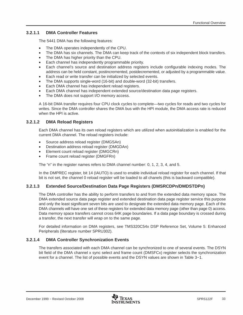
3.2.1.4 DMA Controller Synchronization Events
The transfers associated with each DMA channel can be synchronized to one of several events. The DSYNbit field of the DMA channel x sync select and frame count (DMSFCx) register selects the synchronizationevent for a channel. The list of possible events and the DSYN values are shown in Table 3−1.

Functional Overview
34 December 1999 − Revised October 2008SPRS122F
Table 3−1. DMA Synchronization EventsDSYN VALUE DMA SYNCHRONIZATION EVENT
0000b No synchronization used
0001b McBSP0 Receive Event
0010b McBSP0 Transmit Event
0011b McBSP2 Receive Event
0100b McBSP2 Transmit Event
0101b McBSP1 Receive Event
0110b McBSP1 Transmit Event
0111b − 1111b Reserved
3.2.1.5 DMA Channel Interrupt Selection
The DMA controller can generate a CPU interrupt for each of the six channels. However, channels 0, 1, 2,and 3 are multiplexed with other interrupt sources. DMA channels 0 and 1 share an interrupt line with thereceive and transmit portions of McBSP2 (IMR/IFR bits 6 and 7), and DMA channels 2 and 3 share an interruptline with the receive and transmit portions of McBSP1 (IMR/IFR bits 10 and 11). When the 5441 is reset, theinterrupts from these four DMA channels are deselected. The INTSEL bit field in the DMA channel priority andenable control (DMPREC) register can be used to select these interrupts, as shown in Table 3−2.
Table 3−2. DMA Channel Interrupt SelectionINTSEL Value IMR/IFR[6] IMR/IFR[7] IMR/IFR[10] IMR/IFR[11]
00b (reset) BRINT2 BXINT2 BRINT1 BXINT1
01b BRINT2 BXINT2 DMAC2 DMAC3
10b DMAC0 DMAC1 DMAC2 DMAC3
11b Reserved
3.2.2 16-Bit Bidirectional Host-Port Interface (HPI16)
3.2.2.1 HPI16 Memory Map
The HPI16 is an enhanced 16-bit version of the C54x DSP 8-bit host-port interface (HPI). The HPI16 isdesigned to allow a 16-bit host to access the DSP on-chip memory, with the host acting as the master of theinterface. Each HPI subsystem memory map is identical to its corresponding DMA memory map except theHPI memory map does not support accesses to any memory-mapped registers.
Some of the features of the HPI16 include:
• A 16-bit bidirectional data bus• Multiple data strobes and control signals to allow glueless interfacing to a variety of hosts• Multiplexed and nonmultiplexed address/data modes• A 19-bit address bus used in nonmultiplexed mode to allow access to all on-chip (including extended
address pages) memory• A 19-bit address register used in multiplexed mode. Includes address autoincrement feature for faster
accesses to sequential addresses• Interface to on-chip DMA module to allow access to entire on-chip memory space• HRDY signal to hold off host accesses due to DMA latency• Control register available in multiplexed mode only. Accessible by either host or DSP to provide host/DSP
interrupts, extended addressing, and data prefetch capability• HPI_SEL1 and HPI_SEL2 pins are used to make selection among the four subsystem HPI modules.• Both the HPI data bus and address bus have bus-holder features. The bus holders can be
enabled/disabled by the CPUs.

Functional Overview
35December 1999 − Revised October 2008 SPRS122F
3.2.2.2 HPI Multiplexed Mode
In multiplexed mode, HPI16 operation is very similar to that of the standard 8-bit HPI, which is available withother C54x DSP products. A host with a multiplexed address/data bus can access the HPI16 data register(HPID), address register (HPIA), or control register (HPIC) via the HD bidirectional data bus. The host initiatesthe access with the strobe signals (HDS1, HDS2, HCS) and controls the type of access with the HCNTL,HR/W, and HAS signals. The DSP can interrupt the host via the x_HINT signal, and can stall host accessesvia the HRDY signal. Bit 20 of the HPIA register is used to make selection between program (shared) memoryand data (local) memory access. Table 3−3 shows the memory selection via HA[20].
Table 3−3. HPI Local/Shared Memory Selection Via HA[20]HA[20] Memory Type
0 Local (data)
1 Shared (program)
3.2.2.3 Host/DSP Interrupts
In multiplexed mode, the HPI16 offers the capability for the host and DSP to interrupt each other through theHPIC register.
For host-to-DSP interrupts, the host must write a “1” to the DSPINT bit of the HPIC register. This generatesan interrupt to the DSP. This interrupt can also be used to wake the DSP from any of the IDLE 1,2, or 3 states.Note that the DSPINT bit is always read as “0” by both the host and DSP. The DSP cannot write to this bit (seeFigure 3−12).
For DSP-to-host interrupts, the DSP must write a “1” to the HINT bit of the HPIC register to interrupt the hostvia the x_HINT pin. The host acknowledges and clears this interrupt by also writing a “1” to the HINT bit of theHPIC register. Note that writing a “0” to the HINT bit by either host or DSP has no effect.

Functional Overview
36 December 1999 − Revised October 2008SPRS122F
3.2.2.4 HPI Nonmultiplexed Mode
In nonmultiplexed mode, a host with separate address/data buses can access the HPI16 data register (HPID)via the 16-bit HD bidirectional data bus, and the address register (HPIA) via the 19-bit HA address bus. TheHA[18] signal is used to make selection between program (shared) memory and data (local) memory access.Table 3−4 shows the memory selection via HA[18].
Table 3−4. HPI Local/Shared Memory Selection Via HA[18]HA[18] Memory Type
0 Local (data)
1 Shared (program)
The host initiates the access with the strobe signals (HDS1, HDS2, and HCS) and controls the direction ofthe access with the HR/W signal. The HPI16 can stall host accesses via the HRDY signal. Note that the HPICregister is not available in nonmultiplexed mode since there are no HCNTL signals available. All host accessesinitiate a DMA read or write access. Figure 3−12 shows a block diagram of the HPI16 in nonmultiplexed mode.
HOST HPI-16
Data[15:0]HD[15:0]
R/W HR/WData strobes HDS1, HDS2, HCSHRDY
Ready
HPID[15:0]
ÎÎÎÎÎÎÎÎÎÎÎÎÎÎÎÎÎÎ
DMA
C54xCPU
Inte
rnal
mem
ory
Address[ n:0]†HA[ n :0]†
† n = 0 to 18
Figure 3−12. Interfacing to the HPI-16 in Non-Multiplexed Mode
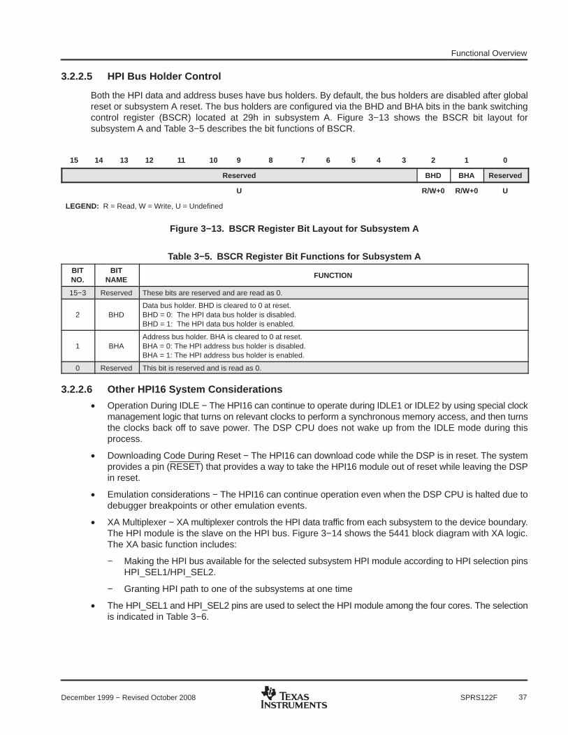
Functional Overview
37December 1999 − Revised October 2008 SPRS122F
3.2.2.5 HPI Bus Holder Control
Both the HPI data and address buses have bus holders. By default, the bus holders are disabled after globalreset or subsystem A reset. The bus holders are configured via the BHD and BHA bits in the bank switchingcontrol register (BSCR) located at 29h in subsystem A. Figure 3−13 shows the BSCR bit layout forsubsystem A and Table 3−5 describes the bit functions of BSCR.
15 14 13 12 11 10 9 8 7 6 5 4 3 2 1 0
Reserved BHD BHA Reserved
U R/W+0 R/W+0 U
LEGEND: R = Read, W = Write, U = Undefined
Figure 3−13. BSCR Register Bit Layout for Subsystem A
Table 3−5. BSCR Register Bit Functions for Subsystem ABITNO.
BITNAME FUNCTION
15−3 Reserved These bits are reserved and are read as 0.
2 BHDData bus holder. BHD is cleared to 0 at reset.BHD = 0: The HPI data bus holder is disabled.BHD = 1: The HPI data bus holder is enabled.
1 BHAAddress bus holder. BHA is cleared to 0 at reset.BHA = 0: The HPI address bus holder is disabled.BHA = 1: The HPI address bus holder is enabled.
0 Reserved This bit is reserved and is read as 0.
3.2.2.6 Other HPI16 System Considerations
• Operation During IDLE − The HPI16 can continue to operate during IDLE1 or IDLE2 by using special clockmanagement logic that turns on relevant clocks to perform a synchronous memory access, and then turnsthe clocks back off to save power. The DSP CPU does not wake up from the IDLE mode during thisprocess.
• Downloading Code During Reset − The HPI16 can download code while the DSP is in reset. The systemprovides a pin (RESET) that provides a way to take the HPI16 module out of reset while leaving the DSPin reset.
• Emulation considerations − The HPI16 can continue operation even when the DSP CPU is halted due todebugger breakpoints or other emulation events.
• XA Multiplexer − XA multiplexer controls the HPI data traffic from each subsystem to the device boundary.The HPI module is the slave on the HPI bus. Figure 3−14 shows the 5441 block diagram with XA logic.The XA basic function includes:
− Making the HPI bus available for the selected subsystem HPI module according to HPI selection pinsHPI_SEL1/HPI_SEL2.
− Granting HPI path to one of the subsystems at one time
• The HPI_SEL1 and HPI_SEL2 pins are used to select the HPI module among the four cores. The selectionis indicated in Table 3−6.

Functional Overview
38 December 1999 − Revised October 2008SPRS122F
DSP Subsystem ADSP ID: 0000
DSP Subsystem BDSP ID: 0001
DSP Subsystem C
DSP ID: 0011DSP Subsystem D
DSP ID: 0010
HPI Bus
HPI Bus
HPI Bus
HPI Bus
HPI_SEL1
HPI_SEL2
XA
NOTE: XA is the MUXing logic for HPI access.
Figure 3−14. XA Multiplexer for HPI Access
Table 3−6. HPI Module Selection
HPI_SEL2 HPI_SEL1 SELECTED HPI MODULE
0 0 Subsystem A
0 1 Subsystem B
1 0 Subsystem C
1 1 Subsystem D

Functional Overview
39December 1999 − Revised October 2008 SPRS122F
3.2.3 Multichannel Buffered Serial Port (McBSP)
The 5441 device provides high-speed, full-duplex serial ports that allow direct interface to other C54x/LC54xdevices, codecs, and other devices in a system. There are twelve multichannel buffered serial ports (McBSPs)on chip (three per subsystem).
The McBSP provides:
• Full-duplex communication• Double-buffer data registers, which allow a continuous data stream• Independent framing and clocking for receive and transmit
In addition, the McBSP has the following capabilities:
• Direct interface to:
− T1/E1 framers
− MVIP switching-compatible and ST-BUS compliant devices
− IOM-2 compliant device
− AC97-compliant device
− Serial peripheral interface (SPI)
• Multichannel transmit and receive of up to 128 channels• A wide selection of data sizes, including: 8, 12, 16, 20, 24, or 32 bits• µ-law and A-law companding• Programmable polarity for both frame synchronization and data clocks• Programmable internal clock and frame generation
3.2.3.1 McBSP Clock Source
The 5441 McBSPs allow either the receive clock pin (BCLKRn) or the transmit clock pin (BCLKXn) to beconfigured as the input clock to the sample rate generator. This enhancement is enabled through two registerbits: bit 7 [the enhanced sample clock mode bit (SCLKME)] of the pin control register (PCR), and bit 13 [theMcBSP sample rate generator clock mode bit (CLKSM)] of the sample rate generator register 2 (SRGR2).SCLKME is an addition to the PCR contained in the McBSPs on previous TMS320C5000 DSP platformdevices. The new bit layout of the PCR is shown in Figure 3−15. For a description of the remaining bits, seeTMS320C54x DSP Reference Set, Volume 5: Enhanced Peripherals (literature number SPRU302).
15 14 13 12 11 10 9 8
Reserved XIOEN RIOEN FSXM FSRM CLKXM CLKRM
R,+0 RW,+0 RW,+0 RW,+0 RW,+0 RW,+0 RW,+0
7 6 5 4 3 2 1 0
SCLKME CLKS_STAT DX_STAT DR_STAT FSXP FSRP CLKXP CLKRP
RW,+0 R,+0 R,+0 R,+0 RW,+0 RW,+0 RW,+0 RW,+0
LEGEND: R = Read, W = Write, +0 = Value at reset
Figure 3−15. Pin Control Register (PCR)
TMS320C5000 is a trademark of Texas Instruments.

Functional Overview
40 December 1999 − Revised October 2008SPRS122F
The selection of the sample rate generator (SRG) clock input source is made by the combination of the CLKSMand SCLKME bit values as shown in Table 3−7.
Table 3−7. Sample Rate Generator Clock Source SelectionSCLKME CLKSM SRG Clock Source
0 0 Reserved
0 1 CPU clock
1 0 BCLKRn pin
1 1 BCLKXn pin
When either of the bidirectional pins, BCLKRn or BCLKXn, is configured as the clock input, its output bufferis automatically disabled. For example, with SCLKME = 1 and CLKSM = 0, the BCLKRn pin is configured asthe SRG input. In this case, both the transmitter and receiver circuits can be synchronized to the SRG outputby setting PCR[9:8] for CLKXM = 1 and CLKRM = 1. However, the SRG output is only driven onto the BCLKXnpin because the BCLKR output is automatically disabled.
3.2.3.2 Multichannel Selection
The McBSP supports independent selection of multiple channels for the transmitter and receiver. Whenmultiple channels are selected, each frame represents a time-division multiplexed (TDM) data stream. In usingtime-division multiplexed data streams, the CPU may only need to process a few of them. Thus, to savememory and bus bandwidth, multichannel selection allows independent enabling of particular channels fortransmission and reception. Up to a maximum of 128 channels in a bit stream can be enabled or disabled.
The 5441 McBSPs have two working modes that are selected by setting the RMCME and XMCME bits in themultichannel control registers MCR1x and MCR2x, respectively (see Figure 3−16 and Figure 3−17). For adescription of the remaining bits, see TMS320C54x DSP Reference Set, Volume 5: Enhanced Peripherals(literature number SPRU302).
• In the first mode, when RMCME = 0 and XMCME = 0, there are two partitions (A and B), with eachcontaining 16 channels as shown in Figure 3−16 and Figure 3−17. This is compatible with the McBSPsused in the 5420, where only 32-channel selection is enabled (default).
15 14 13 12 11 10 9 8 7 6 5 4 3 2 1 0
ReservedXMC
MEXPBBLK XPABLK XCBLK XMCM
R,+0 RW,+0 RW,+0 RW,+0 R,+0 RW,+0
LEGEND: R = Read, W = Write, +0 = Value at reset; x = McBSP 0,1, or 2
Figure 3−16. Multichannel Control Register 2 for McBSPx (MCR2x)
15 14 13 12 11 10 9 8 7 6 5 4 3 2 1 0
ReservedRMC
MERPBBLK RPABLK RCBLK RMCM
R,+0 RW,+0 RW,+0 RW,+0 R,+0 RW,+0
LEGEND: R = Read, W = Write, +0 = Value at reset; x = McBSP 0,1, or 2
Figure 3−17. Multichannel Control Register 1 for McBSPx (MCR1x)

Functional Overview
41December 1999 − Revised October 2008 SPRS122F
• In the second mode, with RMCME = 1 and XMCME = 1, the McBSPs have 128-channel selectioncapability. Twelve registers (RCERCx−RCERHx and XCERCx−XCERHx) are used to enable the128-channel selection. The subaddresses of the registers are shown in Table 3−24. These registers,functionally equivalent to the RCERA0−RCERB1 and XCERA0−XCERB1 registers, are used toenable/disable the transmit and receive of additional channel partitions (C,D,E,F,G, and H) in the128-channel stream. For example, XCERH1 is the transmit enable for channel partition H (channels 112to 127) of McBSP1 for each DSP subsystem. See Figure 3−18, Table 3−8, Figure 3−19, and Table 3−9for bit layouts and functions of the receive and transmit registers.
15 14 13 12 11 10 9 8
RCERyz15 RCERyz14 RCERyz13 RCERyz12 RCERyz11 RCERyz10 RCERyz9 RCERyz8
RW,+0 RW,+0 RW,+0 RW,+0 RW,+0 RW,+0 RW,+0 RW,+0
7 6 5 4 3 2 1 0
RCERyz7 RCERyz6 RCERyz5 RCERy4 RCERyz3 RCERyz2 RCERyz1 RCERyz0
RW,+0 RW,+0 RW,+0 RW,+0 RW,+0 RW,+0 RW,+0 RW,+0
LEGEND: R = Read, W = Write, +0 = Value at reset; y = Partition A,B,C,D,E,F,G, or H; z = McBSP 0,1, or 2
Figure 3−18. Receive Channel Enable Registers Bit Layout for Partitions A to H
Table 3−8. Receive Channel Enable Registers for Partitions A to H
Bit Name Function
15−0 RCERyz[15:0] Receive Channel Enable Register
RCERyz n = 0 Disables reception of nth channel in partition y.
RCERyz n = 1 Enables reception of nth channel in partition y.
Note: y = Partition A,B,C,D,E,F,G, or H; z = McBSP 0,1, or 2; n = bit 15−0
15 14 13 12 11 10 9 8
XCERyz15 XCERyz14 XCERyz13 XCERyz12 XCERyz11 XCERyz10 XCERyz9 XCERyz8
RW,+0 RW,+0 RW,+0 RW,+0 RW,+0 RW,+0 RW,+0 RW,+0
7 6 5 4 3 2 1 0
XCERyz7 XCERyz6 XCERyz5 XCERy4 XCERyz3 XCERyz2 XCERyz1 XCERyz0
RW,+0 RW,+0 RW,+0 RW,+0 RW,+0 RW,+0 RW,+0 RW,+0
LEGEND: R = Read, W = Write, +0 = Value at reset; y = Partition A,B,C,D,E,F,G, or H; z = McBSP 0,1, or 2
Figure 3−19. Transmit Channel Enable Registers Bit Layout for Partitions A to H
Table 3−9. Transmit Channel Enable Registers for Partitions A to H
Bit Name Function
15−0 XCERyz[15:0] Transmit Channel Enable Register
XCERyz n = 0 Disables transmit of nth channel in partition y.
XCERyz n = 1 Enables transmit of nth channel in partition y.
LEGEND: y = Partition A,B,C,D,E,F,G, or H; z = McBSP 0,1, or 2; n = bit 15−0
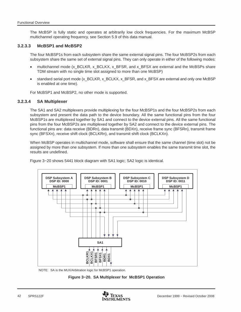
Functional Overview
42 December 1999 − Revised October 2008SPRS122F
The McBSP is fully static and operates at arbitrarily low clock frequencies. For the maximum McBSPmultichannel operating frequency, see Section 5.9 of this data manual.
3.2.3.3 McBSP1 and McBSP2
The four McBSP1s from each subsystem share the same external signal pins. The four McBSP2s from eachsubsystem share the same set of external signal pins. They can only operate in either of the following modes:
• multichannel mode (x_BCLKR, x_BCLKX, x_BFSR, and x_BFSX are external and the McBSPs shareTDM stream with no single time slot assigned to more than one McBSP)
• standard serial port mode (x_BCLKR, x_BCLKX, x_BFSR, and x_BFSX are external and only one McBSPis enabled at one time).
For McBSP1 and McBSP2, no other mode is supported.
3.2.3.4 SA Multiplexer
The SA1 and SA2 multiplexers provide multiplexing for the four McBSP1s and the four McBSP2s from eachsubsystem and present the data path to the device boundary. All the same functional pins from the fourMcBSP1s are multiplexed together by SA1 and connect to the device external pins. All the same functionalpins from the four McBSP2s are multiplexed together by SA2 and connect to the device external pins. Thefunctional pins are: data receive (BDRn), data transmit (BDXn), receive frame sync (BFSRn), transmit framesync (BFSXn), receive shift clock (BCLKRn), and transmit shift clock (BCLKXn).
When McBSP operates in multichannel mode, software shall ensure that the same channel (time slot) not beassigned by more than one subsystem. If more than one subsystem enables the same transmit time slot, theresults are undefined.
Figure 3−20 shows 5441 block diagram with SA1 logic; SA2 logic is identical.
DSP Subsystem ADSP ID: 0000
McBSP1 McBSP1
DSP ID: 0001DSP Subsystem B
McBSP1
DSP ID: 0010DSP Subsystem C
McBSP1
DSP Subsystem DDSP ID: 0011
SA1
BC
LKR
1B
CLK
X1
BF
SR
1B
FS
X1
BD
R1
BD
X1
NOTE: SA is the MUX/Arbitration logic for McBSP1 operation.
Figure 3−20. SA Multiplexer for McBSP1 Operation

Functional Overview
43December 1999 − Revised October 2008 SPRS122F
3.2.4 Hardware Timer
Each 5441 subsystem has one independent software programmable timer. The memory-mapped registerscontrol the operation of the timer. The timer resolution is the clock rate of the CPU. The timer output sharesthe pin with GPIO3 and is controlled by GPIO register bit 15.
The timer supports a 32-bit dynamic range. The timer consists of a programmable 16-bit main counter anda programmable prescalar. The main counter is driven by the prescalar, which decrements by one at everyCPU clock. Once the prescalar reaches zero, the 16-bit counter decrements by one. When the 16-bit counterdecrements to zero, a maskable interrupt (TINT) is generated and the timer output pin (TOUT) asserts anactive-high pulse (2H − 2 ns, H = 0.5 clock cycle). The timer output pulse is driven on GPIO3 when the TOUTbit is set to high in the GPIO register. When the timer is configured in continuous mode, the timer counter andprescalar will be reloaded accordingly after the timer counter exhausts. The timer can be stopped, restarted,reset, or disabled via the bits of the timer control register.
There are four 16-bit registers associated with the timer.
• Timer counter register (TIM)• Timer period register (PRD)• Timer control register (TCR)• Timer second control register (TSCR)
3.2.4.1 TIM Register
This register is loaded with the period register (PRD) value and decrements once the PRD value is loaded.
3.2.4.2 PRD Register
This register is used to reload the timer counter register (TIM).
3.2.4.3 TCR Register
This register provides the control and status information. TCR bit fields are shown in Figure 3−21 anddescribed in Table 3−10.
15 14 13 12 11 10 9 8 7 6 5 4 3 2 1 0
Reserved SOFT FREE PSC TRB TSS TDDR
R/W+0 R/W+0 R/W+0 R/W+0 R/W+0 R/W+0
LEGEND: R = Read, W = Write, +0 = Value at reset
Figure 3−21. Timer Control Register (TCR)

Functional Overview
44 December 1999 − Revised October 2008SPRS122F
Table 3−10. TCR Bit DescriptionBIT
NO.BIT
NAME FUNCTION
15−12 Reserved Register bit is reserved. Read 0, write has no effect.
11 SOFT
Used in conjunction with the FREE bit to determine the state of the timer when a breakpoint is encountered inthe HLL debugger.
When FREE = 0 and SOFT = 0 the timer stops immediately.
When FREE = 0 and SOFT = 1, the timer stops when the counter decrements to 0.
10 FREE
Used in conjunction with the SOFT bit to determine the state of the timer when a breakpoint is encountered inthe HLL debugger.
When FREE = 0, the SOFT bit selects the timer mode.
When FREE = 1, the timer runs free regardless of the SOFT bit.
9−6 PSC Timer prescalar counter, used only when PREMD = 0 (in TSCR register) and the prescaler is in direct mode.
5 TRBTimer reload. When TRB is set, TIM is loaded with the value in the PRD register and the PSC field is loaded withthe value in the TDDR field (when prescalar is in direct mode). TRB is always read a 0.
4 TSS
Timer stop status.
Stops or starts the timer at reset. TSS is cleared and the timer starts timing.
0 = timer is started
1 = timer is stopped
3−0 TDDR
Timer prescalar.
Case 1: When PREMD = 0, TDDR is a 4-bit reload prescalar. When PSC decrements to 0, PSC is loaded withthe contents of TDDR.
Case 2: When PREMD = 1,TDDR is an indirect prescalar, the contents in TDDR is used to specify the timerprescalar.
TDDR[3:0] PRESCALAR
0000 0001h
0001 0003h
0010 0007h
0011 000Fh
0100 001Fh
0101 003Fh
0110 007Fh
0111 00FFh
1000 01FFh
1001 03FFh
1010 07FFh
1011 0FFFh
1100 1FFFh
1101 3FFFh
1110 7FFFh
1111 FFFFh

Functional Overview
45December 1999 − Revised October 2008 SPRS122F
3.2.4.4 TSCR Register
This 16-bit register contains bits to set prescalar mode.
15 14 13 12 11 10 9 8 7 6 5 4 3 2 1 0
Reserved PREMD Reserved
R/W+0
LEGEND: R = Read, W = Write, +0 = Value at reset
Figure 3−22. Timer Second Control Register (TSCR)
Table 3−11. TSCR Bit DescriptionBIT
NO.BIT
NAME FUNCTION
15−13 Reserved Register bit is reserved. Read 0, write has no effect.
12 PREMD
Prescalar mode select bit.
0 = direct mode, TDDR is a 4-bit reload prescalar (default value after reset).
1 = indirect mode, TDDR is used to select individual prescalar value.
11−0 Reserved Register bit is reserved. Read 0, write has no effect.
Out of reset, the TIM and PRD registers are set to a maximum value of FFFFh, the PREMD bit (TSCR[12])is set to 0, the TDDR field (TCR[3:0]) is cleared to 0, and the timer is started.
3.2.5 Watchdog Timer
Each subsystem contains a watchdog timer. The purpose of the watchdog timer is to prevent the system fromlock in case the software becomes trapped in loops with no controlled exit. The watchdog timer has a“watchdog output” pin associated with it. This watchdog output pin is shared with the x_GPIO2/x_WTOUT pin;once the watchdog timer is enabled, this pin is automatically configured as x_WTOUT. The watchdog timerrequires a special service sequence to be executed periodically. Without this periodic servicing, the watchdogtimer counter reaches zero and times out. Consequently, an active-low pulse will be asserted on the “watchdogoutput” pin and an internal maskable interrupt will be triggered. The watchdog output (x_WTOUT) pin can begluelessly external-connected to the local hardware reset or NMI (nonmaskable interrupt). This allowsmaximum flexibility in utilizing the watchdog as required by the particular application.
The watchdog timer is a prescaled 16-bit counter that supports up to a 32-bit dynamic range. Out of reset, thewatchdog is disabled in order to allow as much time as needed for code to be loaded into the 5441 on-chipmemory via the HPI. Prior to being enabled, the watchdog counter will, in fact, still count down from its initialdefault value using the default prescalar value. When the counter reaches zero, a watchdog time-out eventwill occur in that a WD interrupt (WDTINT) request will be sent to the core, and the WDFLAG will be set.However, since all maskable interrupts are disabled by default at reset, the WDTINT will not be serviced bythe core. Additionally, the watchdog pin (x_WTOUT) is disconnected from the watchdog time-out event, sono pulse will be generated on this pin. After this time-out, the counter and prescalar will be reloadedautomatically and the watchdog will continue to count, time out, reload, etc. After code-download, thewatchdog can be enabled to connect the x_WTOUT pin to the time-out event. To enable the watchdog, certainsequence shall be followed as shown in Figure 3−25.
Once the watchdog is enabled, it cannot be disabled by software. It can be disabled by watchdog time-out,local hardware reset, or global hardware reset. A special key sequence is provided to prevent the watchdogfrom being accidentally serviced while the software is trapped in a dead loop or in some other software failures.

Functional Overview
46 December 1999 − Revised October 2008SPRS122F
3.2.5.1 Watchdog Timer Registers
There are four 16-bit registers associated with the watchdog timer.
• WD Timer Counter Register (WDTIM)• WD Timer Period Register (WDPRD)• WD Timer Control Register (WDTCR)• WD Timer Second Control Register (WDTSCR)
3.2.5.2 WDTIM Register
This register contains the 16-bit watchdog counter value. It is decremented once every watchdog clock cycle.
3.2.5.3 WDPRD Register
This register is used to reload the WD timer counter register (WDTIM).
3.2.5.4 WDTCR Register
This register provides the control and status information. WDTCR bit fields are as shown in Figure 3−23 andare described in Table 3−12.
15 14 13 12 11 10 9 8 7 6 5 4 3 2 1 0
Reserved SOFT FREE PSC Reserved TDDR
R/W+0 R/W+0 R R/W+1111
LEGEND: R = Read, W = Write, +0 = Value at reset
Figure 3−23. Watchdog Timer Control Register (WDTCR)

Functional Overview
47December 1999 − Revised October 2008 SPRS122F
Table 3−12. WDTCR Bit DescriptionBIT
NO.BIT
NAME FUNCTION
15−12 Reserved Register bit is reserved. Read 0, write has no effect.
11 SOFT
Used in conjunction with the FREE bit to determine the state of the timer when a breakpoint is encountered inthe HLL debugger.
When FREE = 0 and SOFT = 0 the timer stops immediately.
When FREE = 0 and SOFT = 1, the timer stops when the counter decrements to 0.
10 FREE
Used in conjunction with the SOFT bit to determine the state of the timer when a breakpoint is encountered inthe HLL debugger.
When FREE = 0, the SOFT bit selects the timer mode.
When FREE = 1, the timer runs free regardless of the SOFT bit.
9−6 PSC Timer prescalar counter, used only when PREMD = 0 (in WDTSCR register) and the prescaler is in direct mode.
5−4 Reserved Register bit is reserved. Read 0, write has no effect.
3−0 TDDR
Timer prescalar.
Case 1: When PREMD = 0, TDDR is a 4-bit reload prescalar. When PSC decrements to 0, PSC is loaded withthe contents of TDDR.
Case 2: When PREMD = 1,TDDR is an indirect prescalar, the contents in TDDR is used to specify the timerprescalar.
TDDR[3:0] PRESCALAR
0000 0001h
0001 0003h
0010 0007h
0011 000Fh
0100 001Fh
0101 003Fh
0110 007Fh
0111 00FFh
1000 01FFh
1001 03FFh
1010 07FFh
1011 0FFFh
1100 1FFFh
1101 3FFFh
1110 7FFFh
1111 FFFFh (Default)
3.2.5.5 WDTSCR Register
This 16-bit register contains bits to indicate watchdog flag, to enable watchdog, to set prescalar mode as wellas to provide the 12-bit WDKEY for watchdog service.
WDTSCR bit fields are shown in Figure 3−24 and are described in Table 3−13.

Functional Overview
48 December 1999 − Revised October 2008SPRS122F
15 14 13 12 11 10 9 8 7 6 5 4 3 2 1 0
WDFLAG WDEN Reserved PREMD WDKEY
R/W+0 R/W+0 R/W+1 R/W+0
LEGEND: R = Read, W = Write, +0 = Value at reset
Figure 3−24. Watchdog Timer Second Control Register (WDTSCR)
Table 3−13. WDTSCR Bit DescriptionBIT
NO.BIT
NAME FUNCTION
15 WDFLAG
Watchdog flag bit. This bit can be cleared by enabling the watchdog timer, by device global reset, and by beingwritten with “1”.
It is set by a watchdog time-out.0 = No watchdog time-out occurred1 = Watchdog time-out occurred
14 WDEN
Watchdog timer enable bit.
0 = Watchdog disable. Default value after device reset. Watchdog output pin is disconnected to the
watchdog time-out event, counter starts to run.
1 = Watchdog enable. Once enabled, the watchdog output pin is connected to the watchdog time-out
event, and can be disabled by watchdog time-out or reset.
13 Reserved Register bit is reserved. Read 0, write has no effect.
12 PREMD
Prescalar mode select bit.
0 = Direct mode, TDDR is 4-bit reload prescalar.
1 = Indirect mode, TDDR is used to select individual prescalar value (default value after local or global
hardware reset).
11−0 WDKEY 12-bit watchdog reset key, only the sequence of a 5C6h followed by an A7Eh services the watchdog.
The watchdog has to be serviced periodically with the sequence of 5C6h followed by A7Eh, written to WDKEYbefore the watchdog timer times out. Both 5C6h and A7Eh are allowed to be written to WDKEY. Only thesequence of 5C6h followed by A7Eh, to WDKEY services the watchdog. Any other writes to WDKEY willtrigger the watchdog time-out immediately, and consequently:
• the watchdog output pin will generate an active-low pulse (6H ns, H=0.5 clock cycle)• the WDFLAG bit in WDTSCR will be set to 1• the internal maskable WD interrupt (WD_TINT) will be triggered
Read from WDTSCR register will not cause time-out.
When the watchdog is in time-out state, the watchdog is disabled and WDEN is cleared. The watchdog outputpin (x_WTOUT) is disconnected to the watchdog time-out event. Finally, the timer is reloaded and continuesto run.
Out of reset, the watchdog is disabled, and reads and writes to the watchdog registers are allowed. Once 5C6his written to WDKEY in the WDTSCR register from the initial state, the watchdog enters the preactive state.The next write to the WDTSCR register should be completed with a “1” written to WDEN and A7Eh writtento WDKEY. This causes the watchdog timer to enter the active state. Once the watchdog is enabled, it cannotbe disabled by software. Any writes to the WDTSCR register from the active or service states that do not write5C6h or A7Eh to WDKEY will result in an immediate watchdog time-out. Writing the sequence of 5C6h andA7Eh to WDKEY causes the watchdog timer to transition between the active and service states. The transitionfrom the service state to the active state results in the timer register reload that is necessary to keep thewatchdog timer from timing out. Each time the watchdog is serviced by the sequence, the watchdog timercounter and prescalar will automatically be reloaded.

Functional Overview
49December 1999 − Revised October 2008 SPRS122F
The registers WDTIM, WDPRD, WDTCR, and the PREMD bit in WDTSCR must be configured before thewatchdog enters the active state. By default, WDTIM =FFFFh, WDPRD = FFFFh, PREMD = 1, TDDR = 1111b.Writing a ‘1’ to WDEN and configuring the PREMD bit must be done at the same time that A7Eh is written toWDKEY in watchdog pre-active state.
3.2.5.6 Watchdog State Diagram
Figure 3−25 shows the watchdog operation state diagram.
Initial State(WatchdogDisabled)
(WDTIM=FFFFh)(WDPRD=FFFFh)
(TDDR=1111b)(PREMD=1)
Power Up/Reset
(Hardware)
Not 5C6h toWDKEY
5C6h to WDKEY
Pre-ActiveState
5C6h toWDKEY
A7Eh toWDKEY
A7Eh to WDKEYwith ”1” to WDEN
(Reload Timer,Clear WDFLAG,
Enable Output Pin)Active State(Waiting for
5C6h)
Not A7Eh or 5C6hto WDKEY Not 5C6h or A7Eh
to WDKEYOutput Pin Asserted
WDFLAG SetWD INT Triggered
Timeout!Output Pin Asserted
WDFLAG SetWD INT Triggered
TimeoutState
(WatchdogDisabled)
(Output PinDisconnected)
5C6h toWDKEY
A7Eh toWDKEY(RegisterReload)
ServiceState
(Waiting forA7Eh)
5C6h toWDKEY
Timeout!
WDFLAG SetWD INT Triggered
Output Pin Asserted
WD INT Triggered
to WDKEYOutput Pin Asserted
WDFLAG Set
Not A7Eh or 5C6h
Figure 3−25. Watchdog Operation State Diagram
As shown in Figure 3−25, the watchdog is disabled before it enters the active state. Even though disabled,the WD interrupt (WD_TINT) may be triggered periodically although the watchdog output pin (x_WTOUT) willnot be asserted. The interrupt may be utilized to:
• Indicate that watchdog is not in active state• Allow the watchdog timer to act as a general-purpose time counter if the watchdog functionality is not
needed.
3.2.5.7 Watchdog Register Write Protection
Once the watchdog is enabled, writes to registers WDTIM, WDPRD, and WDTCR will have no effect. Writesto the WDFLAG, WDEN, and PREMD bits in register WDTSCR will have no effect. However, writing anincorrect key (not 5C6h or A7Eh) to WDKEY will result in an immediate time-out.

Functional Overview
50 December 1999 − Revised October 2008SPRS122F
3.2.6 Software-Programmable Phase-Locked Loop (PLL)
The clock generator provides clocks to the 5441 device, and consists of a phase-locked loop (PLL) circuit. Theclock generator requires a reference clock input, which must be provided by using an external clock source.The reference clock input is then divided by two (DIV mode) to generate clocks for the 5441 device. Alternately,the PLL circuit can be used (PLL mode) to generate the device clock by multiplying the reference clockfrequency by a scale factor, allowing use of a clock source with a lower frequency than that of the CPU. ThePLL is an adaptive circuit that, once synchronized, locks onto and tracks an input clock signal. When the PLLis initially started, it enters a transitional mode during which the PLL acquires lock with the input signal. Oncethe PLL is locked, it continues to track and maintain synchronization with the input signal. Then, other internalclock circuitry allows the synthesis of new clock frequencies for use as master clock for the 5441 device. Onlysubsystem A controls the PLL. Subsystems B, C, and D cannot access the PLL registers.
The software-programmable PLL features a high level of flexibility, and includes a clock scaler that providesvarious clock multiplier ratios, capability to directly enable and disable the PLL, and a PLL lock timer that canbe used to delay switching to PLL clocking mode of the device until lock is achieved. Devices that have abuilt-in software-programmable PLL can be configured in one of two clock modes:
• PLL mode. The input clock (CLKIN) is multiplied by 1 of 31 possible ratios. These ratios are achieved usingthe PLL circuitry.
• DIV (divider) mode. The input clock is divided by 2 or 4. Note that when DIV mode is used, the PLL canbe completely disabled in order to minimize power dissipation.
The software-programmable PLL is controlled using the 16-bit memory-mapped (address 0058h) clock moderegister (CLKMD). The CLKMD register is used to define the clock configuration of the PLL clock module.Figure 3−26 shows the bit layout of the clock mode register and Table 3−14 describes the bit functions.
15 12 11 10 3 2 1 0
PLLMUL † PLLDIV† PLLCOUNT† PLLON/OFF† PLLNDIV STATUS
R/W R/W R/W R/W R/W R/W
†When in DIV mode (PLLSTATUS is low), PLLMUL, PLLDIV, PLLCOUNT, and PLLON/OFF are don’t cares, and their contents are indeterminate.
LEGEND: R = Read, W = Write
Figure 3−26. Clock Mode Register (CLKMD)

Functional Overview
51December 1999 − Revised October 2008 SPRS122F
Table 3−14. Clock Mode Register (CLKMD) Bit FunctionsBIT
NO.BIT
NAME FUNCTION
15−12 PLLMUL† PLL multiplier. PLLMUL defines the frequency multiplier in conjunction with PLLDIV and PLLNDIV. SeeTable 3−15.
PLL divider. PLLDIV defines the frequency multiplier in conjunction with PLLMUL and PLLNDIV. See Table 3−15.
11 PLLDIV† PLLDIV = 0 Means that an integer multiply factor is used11 PLLDIV†
PLLDIV = 1 Means that a noninteger multiply factor is used
10−3 PLLCOUNT†
PLL counter value. PLLCOUNT specifies the number of input clock cycles (in increments of16 cycles) for the PLLlock timer to count before the PLL begins clocking the processor after the PLL is started. The PLL counter is adown-counter, which is driven by the input clock divided by 16; therefore, for every 16 input clocks, the PLLcounter decrements by one.
The PLL counter can be used to ensure that the processor is not clocked until the PLL is locked, so that only validclock signals are sent to the device.
2 PLLON/OFF†PLL on/off. PLLON/OFF enables or disables the PLL part of the clock generator in conjunction with the PLLNDIVbit (see Table 3−16). Note that PLLON/OFF and PLLNDIV can both force the PLL to run; when PLLON/OFF ishigh, the PLL runs independently of the state of PLLNDIV.
1 PLLNDIVPLLNDIV configures PLL mode when high or DIV mode when low. PLLNDIV defines the frequency multiplier inconjunction with PLLDIV and PLLMUL. See Table 3−15.
Indicates the PLL mode.
0 STATUS STATUS = 0 Indicates DIV mode0 STATUS
STATUS = 1 Indicates PLL mode
†When in DIV mode (PLLSTATUS is low), PLLMUL, PLLDIV, PLLCOUNT, and PLLON/OFF are don’t cares, and their contents are indeterminate.
Table 3−15. Multiplier Related to PLLNDIV, PLLDIV, and PLLMULPLLNDIV PLLDIV PLLMUL MULTIPLIER‡
0 x 0−14 0.5
0 x 15 0.25
1 0 0−14 PLLMUL + 1
1 0 15 bypass (multiply by 1)
1 1 0 or even (PLLMUL + 1)/2
1 1 odd PLLMUL/4‡ CLKOUT = CLKIN * Multiplier
Table 3−16. VCO Truth TablePLLON/OFF PLLNDIV VCO STATE
0 0 off
1 0 on
0 1 on
1 1 on
3.2.6.1 PLL Clock Programmable Timer
During the lockup period, the PLL should not be used to clock the 5441. The PLLCOUNT programmable locktimer provides a convenient method of automatically delaying clocking of the device by the PLL until lock isachieved.
The PLL lock timer is a counter, loaded from the PLLCOUNT field in the CLKMD register, that decrements fromits preset value to 0. The timer can be preset to any value from 0 to 255, and its input clock is CLKIN dividedby 16. The resulting lockup delay can therefore be set from 0 to 255 × 16 CLKIN cycles.

Functional Overview
52 December 1999 − Revised October 2008SPRS122F
The lock timer is activated when the operating mode of the clock generator is switched from DIV to PLL. Duringthe lockup period, the clock generator continues to operate in DIV mode; after the PLL lock timer decrementsto zero, the PLL begins clocking the 5441.
Accordingly, the value loaded into PLLCOUNT is chosen based on the following formula:
PLLCOUNT Lockup Time16 TCLKIN
where TCLKIN is the input reference clock period and lockup time is the required VCO lockup time, as shownin Table 3−17.
Table 3−17. VCO Lockup TimeCLKOUT FREQUENCY (MHz) LOCKUP TIME (µs)†
5 23
10 17
20 16
40 19
60 24
80 29
100 35
135 45† Approximate values
3.2.6.2 CLKMD Register Initialization At Reset
The clock mode pin (CLKMD) is used to initialize the PLL to a known value at reset. The CLKMD pin is sampledwhen the reset signal is low. Only global reset (RESET) will reset the PLL. Subsystem A local reset (A_RS)has no effect on the PLL.
Table 3−18. PLL Initialization at ResetCLKMD PIN PLL MODE
0 Bypass
1 CLKINx2
3.2.7 General-Purpose I/O
The 5441 has 16 general-purpose I/O pins. These pins are:
A_GPIO0, A_GPIO1, A_GPIO2, A_GPIO3
B_GPIO0, B_GPIO1, B_GPIO2, B_GPIO3
C_GPIO0, C_GPIO1, C_GPIO2, C_GPIO3
D_GPIO0, D_GPIO1, D_GPIO2, D_GPIO3
Four bits of general-purpose I/O are available to each core. Each GPIO pin can be individually selected aseither an input or an output through the GPIO register. The x_XF, x_BIO, and timer output are selectable onGPIO pins 0, 1, and 3 through the GPIO register also. Each output driver has an independent three-statecontrol. All nonreserved GPIO register bits are readable and writeable. The GPIO register bits will be setto 0 when the core is in reset, which will configure all GPIO as inputs. GPIO data and control bits are accessiblethrough a memory-mapped register at 3Ch with the format shown in Figure 3−27 and the bit functionsdescribed in Table 3−19.

Functional Overview
53December 1999 − Revised October 2008 SPRS122F
15 14 13 12 11 10 9 8 7 6 5 4 3 2 1 0
TOUT Rsvd X_BIO X_XFGPIODIR3
GPIODIR2
GPIODIR1
GPIODIR0
CLKOUT1
CLKOUT0 Reserved
GPIODAT3
GPIODAT2
GPIODAT1
GPIODAT0
R/W+0 R/W+0 R/W+0 R/W+0 R/W+0 R/W+0 R/W+0 R/W+0 R/W+0 R/W+0 R/W+0 R/W+0 R/W+0
LEGEND: R = Read, W = Write, +0 = Value at reset
Figure 3−27. General-Purpose I/O Control Register
Table 3−19. General-Purpose I/O Control Register Bit FunctionsBITNO.
BITNAME
BITVALUE FUNCTION
15 TOUT0 Timer output disable. Uses GPIO3 as general-purpose I/O.
15 TOUT1 Timer output enable. Overrides DIR3. Timer output is driven on GPIO3 and readable in DAT3.
14 Reserved X Register bit is reserved. Read 0, write has no effect.
0 Branch control input disable. Uses GPIO1 as general-purpose I/O.
13 X_BIO1
Branch control input enable. Overrides DIR1. The X_BIO output is driven on GPIO1 and readable inDAT0.
12 X_XF0 External flag output disable. Uses GPIO0 as general-purpose I/O.
12 X_XF1 External flag output enable. Overrides DIR0. The X_XF output is driven on GPIO0 and readable in DAT1.
11−8GPIO 0 GPIOn pin is used as an input.
11−8GPIO
DIRn† 1 GPIOn pin is used as an output.
7−6 CLKOUT
CLKOUT muxing selection bits.
CLKOUT1[7] CLKOUT0[6]
A_CLKOUT 0 0(default)
B_CLKOUT 0 1
C_CLKOUT 1 0
D_CLKOUT 1 1
5−4 Reserved X Register bit is reserved. Read 0, write has no effect.
3−0GPIO
†0 GPIOn is driven with a 0 (DIRn = 1). GPIOn is read as 0 (DIRn = 0).
3−0GPIODATn† 1 GPIOn is driven with a 1 (DIRn = 1). GPIOn is read as 1 (DIRn = 0).
† n = 3, 2, 1, or 0
The timer output (TOUT) bit is used to multiplex the output of the timer and GPIO3. The X_XF bit is used tomultiplex the output of the external flag, and the X_BIO bit is used to multiplex the input of the branch control.The watchdog enable (WDEN) bit in the watchdog timer second control register (WDTSCR) is used tomultiplex the watchdog timer output and GPIO2. All GPIO pins are programmable as an input or output by thedirection bit (GPIODIRn). Data is either driven or read from the data bit field (GPIODATn). GPIODIR3 has noeffect when TOUT = 1.

Functional Overview
54 December 1999 − Revised October 2008SPRS122F
3.2.8 Chip Subsystem ID Register
The chip subsystem ID register (CSIDR) is a read-only memory-mapped register located at 3Eh within eachDSP subsystem. This register contains two elements for electrically readable device identification. TheChip ID bits identify the type of C54x device (41h for 5441). The SubSysID contains a unique subsystemidentifier. Figure 3−28 shows the CSIDR and Table 3−20 describes its bit functions.
15 14 13 12 11 10 9 8 7 6 5 4 3 2 1 0
Chip ID Reserved SubSysID
R R
LEGEND: R = Read
Figure 3−28. Chip Subsystem ID Register (CSIDR)
Table 3−20. Chip Subsystem ID Register Bit FunctionsBITNO.
BIT FIELDNAME FUNCTION
15−8 Chip ID 54x device type. Contains 41h for 5441.15−8 Chip ID 54x device type. Contains 41h for 5441.
7−4 Reserved
3−0 SubSysID Identifier for DSP subsystem: A = 00b, B = 01b, C = 10b, and D = 11b3−0 SubSysID Identifier for DSP subsystem: A = 00b, B = 01b, C = 10b, and D = 11b
3.2.9 Data Memory Map Register
To access the extended data memory, the DSP CPU need to configure the data memory map register(DMMR), which is used to point to extended data memory. The content of DMMR register is used to selectthe extended data for all CPU data memory accesses. Figure 3−29 shows the DMMR and Table 3−21describes its bit functions.
15 14 13 12 11 10 9 8 7 6 5 4 3 2 1 0
ReservedExtended
Data
R/W+0
LEGEND: R = Read, W = Write
Figure 3−29. Data Memory Map Register (DMMR)
Table 3−21. Data Memory Map Register FunctionsBITNO.
BIT FIELDNAME FUNCTION
15−1 Reserved
0 Extended data
Extended data memory for CPU access:
Extended_Data = 0b, DARAM2 and DARAM3 are mapped in.0 Extended data Extended_Data = 0b, DARAM2 and DARAM3 are mapped in.
Extended_Data = 1b, DARAM4 and DARAM5 are mapped in.

Functional Overview
55December 1999 − Revised October 2008 SPRS122F
3.3 Memory-Mapped Registers
The 5441 has 27 processor memory-mapped registers, which are mapped in data memory space addresses0h to 1Fh as shown in Table 3−22. Each device also has a set of memory-mapped registers associated withthe peripherals as shown in Table 3−23.
Table 3−22. Processor Memory-Mapped Registers for Each DSP Subsystem
NAMEADDRESS
DESCRIPTIONNAMEDEC HEX
DESCRIPTION
IMR 0 0 Interrupt Mask Register
IFR 1 1 Interrupt Flag Register
— 2−5 2−5 Reserved for testing
ST0 6 6 Status Register 0
ST1 7 7 Status Register 1
AL 8 8 Accumulator A Low Word (15−0)
AH 9 9 Accumulator A High Word (31−16)
AG 10 A Accumulator A Guard Bits (39−32)
BL 11 B Accumulator B Low Word (15−0)
BH 12 C Accumulator B High Word (31−16)
BG 13 D Accumulator B Guard Bits (39−32)
TREG 14 E Temporary Register
TRN 15 F Transition Register
AR0 16 10 Auxiliary Register 0
AR1 17 11 Auxiliary Register 1
AR2 18 12 Auxiliary Register 2
AR3 19 13 Auxiliary Register 3
AR4 20 14 Auxiliary Register 4
AR5 21 15 Auxiliary Register 5
AR6 22 16 Auxiliary Register 6
AR7 23 17 Auxiliary Register 7
SP 24 18 Stack Pointer
BK 25 19 Circular Buffer Size Register
BRC 26 1A Block-Repeat Counter
RSA 27 1B Block-Repeat Start Address
REA 28 1C Block-Repeat End Address
PMST 29 1D Processor Mode Status Register
XPC 30 1E Extended Program Counter
— 31 1F Reserved

Functional Overview
56 December 1999 − Revised October 2008SPRS122F
Table 3−23. Peripheral Memory-Mapped Registers for Each DSP Subsystem
NAMEADDRESS
(HEX) DESCRIPTION
DRR20 20 McBSP 0 Data Receive Register 2
DRR10 21 McBSP 0 Data Receive Register 1
DXR20 22 McBSP 0 Data Transmit Register 2
DXR10 23 McBSP 0 Data Transmit Register 1
TIM 24 Timer Register
PRD 25 Timer Period Register
TCR 26 Timer Control Register
TSCR 27 Timer Second Control Register
− 28 Reserved
BSCR 29 Bank-Switching Control Register
— 2A−2B Reserved
HPIC 2C HPI Control Register (HMODE=0 only)
— 2D−2F Reserved
DRR22 30 McBSP 2 Data Receive Register 2
DRR12 31 McBSP 2 Data Receive Register 1
DXR22 32 McBSP 2 Data Transmit Register 2
DXR12 33 McBSP 2 Data Transmit Register 1
SPSA2 34 McBSP 2 Subbank Address Register†
SPSD2 35 McBSP 2 Subbank Data Register†
— 36−37 Reserved
SPSA0 38 McBSP 0 Subbank Address Register†
SPSD0 39 McBSP 0 Subbank Data Register†
— 3A−3B Reserved
GPIO 3C General-Purpose I/O Register
— 3D Reserved
CSIDR 3E Chip Subsystem ID register
— 3F Reserved
DRR21 40 McBSP 1 Data Receive Register 2
DRR11 41 McBSP 1 Data Receive Register 1
DXR21 42 McBSP 1 Data Transmit Register 2
DXR11 43 McBSP 1 Data Transmit Register 1
— 44−47 Reserved
SPSA1 48 McBSP 1 Subbank Address Register†
SPSD1 49 McBSP 1 Subbank Data Register†
— 4A−4B Reserved
TIM 4C Watchdog Timer Register
PRD 4D Watchdog Timer Period Register
TCR 4E Watchdog Timer Control Register
WDTSCR 4F Watchdog Timer Second Control Register
DMMR 50 Data Memory Map Register
— 51−53 Reserved
DMPREC 54 DMA Priority and Enable Control Register
DMSA 55 DMA Subbank Address Register‡
DMSDI 56 DMA Subbank Data Register with Autoincrement‡
†See Table 3−24 for a detailed description of the McBSP control registers and their subaddresses.‡See Table 3−25 for a detailed description of the DMA subbank addressed registers.

Functional Overview
57December 1999 − Revised October 2008 SPRS122F
Table 3−23. Peripheral Memory-Mapped Registers for Each DSP Subsystem (Continued)
NAME DESCRIPTIONADDRESS
(HEX)
DMSDN 57 DMA Subbank Data Register‡
CLKMD 58 Clock Mode Register (CLKMD), subsystem A only (reserved in subsystems B, C, and D)
— 59−5F Reserved†See Table 3−24 for a detailed description of the McBSP control registers and their subaddresses.‡See Table 3−25 for a detailed description of the DMA subbank addressed registers.
3.4 McBSP Control Registers and Subaddresses
The control registers for the multichannel buffered serial port (McBSP) are accessed using the subbankaddressing scheme. This allows a set or subbank of registers to be accessed through a single memorylocation. The McBSP subbank address register (SPSAx) is used as a pointer to select a particular registerwithin the subbank. The McBSP data register (SPSDx) is used to access (read or write) the selected register.Table 3−24 shows the McBSP control registers and their corresponding subaddresses.
Table 3−24. McBSP Control Registers and SubaddressesMcBSP0 McBSP1 McBSP2 SUB-
DESCRIPTIONNAME ADDRESS NAME ADDRESS NAME ADDRESS
SUB-ADDRESS
DESCRIPTION
ÁÁÁÁÁÁÁÁ
SPCR10ÁÁÁÁÁÁÁÁ
39h ÁÁÁÁÁÁÁÁ
SPCR11ÁÁÁÁÁÁÁÁ
49h ÁÁÁÁÁÁÁÁ
SPCR12ÁÁÁÁÁÁÁÁ
35h ÁÁÁÁÁÁÁÁÁÁ
00h ÁÁÁÁÁÁÁÁÁÁÁÁÁÁÁÁÁÁÁÁÁÁ
Serial port control register 1
ÁÁÁÁÁÁÁÁ
SPCR20ÁÁÁÁÁÁÁÁ
39h ÁÁÁÁÁÁÁÁ
SPCR21ÁÁÁÁÁÁÁÁ
49h ÁÁÁÁÁÁÁÁ
SPCR22ÁÁÁÁÁÁÁÁ
35h ÁÁÁÁÁÁÁÁÁÁ
01h ÁÁÁÁÁÁÁÁÁÁÁÁÁÁÁÁÁÁÁÁÁÁ
Serial port control register 2
ÁÁÁÁRCR10 ÁÁÁÁ39h ÁÁÁÁRCR11ÁÁÁÁ49h ÁÁÁÁRCR12ÁÁÁÁ35h ÁÁÁÁÁ02h ÁÁÁÁÁÁÁÁÁÁÁReceive control register 1ÁÁÁÁÁÁÁÁRCR20
ÁÁÁÁÁÁÁÁ39h
ÁÁÁÁÁÁÁÁRCR21
ÁÁÁÁÁÁÁÁ49h
ÁÁÁÁÁÁÁÁRCR22
ÁÁÁÁÁÁÁÁ35h
ÁÁÁÁÁÁÁÁÁÁ03h
ÁÁÁÁÁÁÁÁÁÁÁÁÁÁÁÁÁÁÁÁÁÁReceive control register 2ÁÁÁÁ
ÁÁÁÁXCR10ÁÁÁÁÁÁÁÁ39h
ÁÁÁÁÁÁÁÁXCR11
ÁÁÁÁÁÁÁÁ49h
ÁÁÁÁÁÁÁÁXCR12
ÁÁÁÁÁÁÁÁ35h
ÁÁÁÁÁÁÁÁÁÁ04h
ÁÁÁÁÁÁÁÁÁÁÁÁÁÁÁÁÁÁÁÁÁÁTransmit control register 1ÁÁÁÁ
ÁÁÁÁXCR20
ÁÁÁÁÁÁÁÁ
39hÁÁÁÁÁÁÁÁ
XCR21ÁÁÁÁÁÁÁÁ
49hÁÁÁÁÁÁÁÁ
XCR22ÁÁÁÁÁÁÁÁ
35hÁÁÁÁÁÁÁÁÁÁ
05hÁÁÁÁÁÁÁÁÁÁÁÁÁÁÁÁÁÁÁÁÁÁ
Transmit control register 2ÁÁÁÁÁÁÁÁ
SRGR10ÁÁÁÁÁÁÁÁ
39h ÁÁÁÁÁÁÁÁ
SRGR11ÁÁÁÁÁÁÁÁ
49h ÁÁÁÁÁÁÁÁ
SRGR12ÁÁÁÁÁÁÁÁ
35h ÁÁÁÁÁÁÁÁÁÁ
06h ÁÁÁÁÁÁÁÁÁÁÁÁÁÁÁÁÁÁÁÁÁÁ
Sample rate generator register 1ÁÁÁÁÁÁÁÁ
SRGR20ÁÁÁÁÁÁÁÁ
39h ÁÁÁÁÁÁÁÁ
SRGR21ÁÁÁÁÁÁÁÁ
49h ÁÁÁÁÁÁÁÁ
SRGR22ÁÁÁÁÁÁÁÁ
35h ÁÁÁÁÁÁÁÁÁÁ
07h ÁÁÁÁÁÁÁÁÁÁÁÁÁÁÁÁÁÁÁÁÁÁ
Sample rate generator register 2
ÁÁÁÁÁÁÁÁ
MCR10 ÁÁÁÁÁÁÁÁ
39h ÁÁÁÁÁÁÁÁ
MCR11ÁÁÁÁÁÁÁÁ
49h ÁÁÁÁÁÁÁÁ
MCR12ÁÁÁÁÁÁÁÁ
35h ÁÁÁÁÁÁÁÁÁÁ
08h ÁÁÁÁÁÁÁÁÁÁÁÁÁÁÁÁÁÁÁÁÁÁ
Multichannel register 1
ÁÁÁÁÁÁÁÁ
MCR20 ÁÁÁÁÁÁÁÁ
39h ÁÁÁÁÁÁÁÁ
MCR21ÁÁÁÁÁÁÁÁ
49h ÁÁÁÁÁÁÁÁ
MCR22ÁÁÁÁÁÁÁÁ
35h ÁÁÁÁÁÁÁÁÁÁ
09h ÁÁÁÁÁÁÁÁÁÁÁÁÁÁÁÁÁÁÁÁÁÁ
Multichannel register 2
ÁÁÁÁÁÁÁÁ
RCERA0ÁÁÁÁÁÁÁÁ
39h ÁÁÁÁÁÁÁÁ
RCERA1ÁÁÁÁÁÁÁÁ
49h ÁÁÁÁÁÁÁÁ
RCERA2ÁÁÁÁÁÁÁÁ
35h ÁÁÁÁÁÁÁÁÁÁ
0Ah ÁÁÁÁÁÁÁÁÁÁÁÁÁÁÁÁÁÁÁÁÁÁ
Receive channel enable register partition A
ÁÁÁÁRCERB0ÁÁÁÁ39h ÁÁÁÁRCERB1ÁÁÁÁ49h ÁÁÁÁRCERB2ÁÁÁÁ35h ÁÁÁÁÁ0Bh ÁÁÁÁÁÁÁÁÁÁÁReceive channel enable register partition BÁÁÁÁÁÁÁÁXCERA0
ÁÁÁÁÁÁÁÁ39h
ÁÁÁÁÁÁÁÁXCERA1
ÁÁÁÁÁÁÁÁ49h
ÁÁÁÁÁÁÁÁXCERA2
ÁÁÁÁÁÁÁÁ35h
ÁÁÁÁÁÁÁÁÁÁ0Ch
ÁÁÁÁÁÁÁÁÁÁÁÁÁÁÁÁÁÁÁÁÁÁTransmit channel enable register partition AÁÁÁÁ
ÁÁÁÁXCERB0
ÁÁÁÁÁÁÁÁ
39hÁÁÁÁÁÁÁÁ
XCERB1ÁÁÁÁÁÁÁÁ
49hÁÁÁÁÁÁÁÁ
XCERB2ÁÁÁÁÁÁÁÁ
35hÁÁÁÁÁÁÁÁÁÁ
0DhÁÁÁÁÁÁÁÁÁÁÁÁÁÁÁÁÁÁÁÁÁÁ
Transmit channel enable register partition BÁÁÁÁÁÁÁÁ
PCR0ÁÁÁÁÁÁÁÁ
39hÁÁÁÁÁÁÁÁ
PCR1ÁÁÁÁÁÁÁÁ
49hÁÁÁÁÁÁÁÁ
PCR2ÁÁÁÁÁÁÁÁ
35hÁÁÁÁÁÁÁÁÁÁ
0EhÁÁÁÁÁÁÁÁÁÁÁÁÁÁÁÁÁÁÁÁÁÁ
Pin control registerÁÁÁÁÁÁÁÁ
RCERC0ÁÁÁÁÁÁÁÁ
39h ÁÁÁÁÁÁÁÁ
RCERC1ÁÁÁÁÁÁÁÁ
49h ÁÁÁÁÁÁÁÁ
RCERC2ÁÁÁÁÁÁÁÁ
35h ÁÁÁÁÁÁÁÁÁÁ
010h ÁÁÁÁÁÁÁÁÁÁÁÁÁÁÁÁÁÁÁÁÁÁ
Receive channel enable register partition C
ÁÁÁÁÁÁÁÁ
RCERD0ÁÁÁÁÁÁÁÁ
39h ÁÁÁÁÁÁÁÁ
RCERD1ÁÁÁÁÁÁÁÁ
49h ÁÁÁÁÁÁÁÁ
RCERD2ÁÁÁÁÁÁÁÁ
35h ÁÁÁÁÁÁÁÁÁÁ
011h ÁÁÁÁÁÁÁÁÁÁÁÁÁÁÁÁÁÁÁÁÁÁ
Receive channel enable register partition D
ÁÁÁÁÁÁÁÁ
XCERC0ÁÁÁÁÁÁÁÁ
39h ÁÁÁÁÁÁÁÁ
XCERC1ÁÁÁÁÁÁÁÁ
49h ÁÁÁÁÁÁÁÁ
XCERC2ÁÁÁÁÁÁÁÁ
35h ÁÁÁÁÁÁÁÁÁÁ
012h ÁÁÁÁÁÁÁÁÁÁÁÁÁÁÁÁÁÁÁÁÁÁ
Transmit channel enable register partition C
ÁÁÁÁÁÁÁÁ
XCERD0ÁÁÁÁÁÁÁÁ
39h ÁÁÁÁÁÁÁÁ
XCERD1ÁÁÁÁÁÁÁÁ
49h ÁÁÁÁÁÁÁÁ
XCERD2ÁÁÁÁÁÁÁÁ
35h ÁÁÁÁÁÁÁÁÁÁ
013h ÁÁÁÁÁÁÁÁÁÁÁÁÁÁÁÁÁÁÁÁÁÁ
Transmit channel enable register partition D
ÁÁÁÁRCERE0ÁÁÁÁ39h ÁÁÁÁRCERE1ÁÁÁÁ49h ÁÁÁÁRCERE2ÁÁÁÁ35h ÁÁÁÁÁ014h ÁÁÁÁÁÁÁÁÁÁÁReceive channel enable register partition EÁÁÁÁÁÁÁÁRCERF0
ÁÁÁÁÁÁÁÁ39h
ÁÁÁÁÁÁÁÁRCERF1
ÁÁÁÁÁÁÁÁ49h
ÁÁÁÁÁÁÁÁRCERF2
ÁÁÁÁÁÁÁÁ35h
ÁÁÁÁÁÁÁÁÁÁ015h
ÁÁÁÁÁÁÁÁÁÁÁÁÁÁÁÁÁÁÁÁÁÁReceive channel enable register partition FÁÁÁÁ
ÁÁÁÁXCERE0ÁÁÁÁÁÁÁÁ39h
ÁÁÁÁÁÁÁÁXCERE1
ÁÁÁÁÁÁÁÁ49h
ÁÁÁÁÁÁÁÁXCERE2
ÁÁÁÁÁÁÁÁ35h
ÁÁÁÁÁÁÁÁÁÁ016h
ÁÁÁÁÁÁÁÁÁÁÁÁÁÁÁÁÁÁÁÁÁÁTransmit channel enable register partition EÁÁÁÁ
ÁÁÁÁXCERF0
ÁÁÁÁÁÁÁÁ
39hÁÁÁÁÁÁÁÁ
XCERF1ÁÁÁÁÁÁÁÁ
49hÁÁÁÁÁÁÁÁ
XCERF2ÁÁÁÁÁÁÁÁ
35hÁÁÁÁÁÁÁÁÁÁ
017hÁÁÁÁÁÁÁÁÁÁÁÁÁÁÁÁÁÁÁÁÁÁ
Transmit channel enable register partition FÁÁÁÁÁÁÁÁ
RCERG0ÁÁÁÁÁÁÁÁ
39h ÁÁÁÁÁÁÁÁ
RCERG1ÁÁÁÁÁÁÁÁ
49h ÁÁÁÁÁÁÁÁ
RCERG2ÁÁÁÁÁÁÁÁ
35h ÁÁÁÁÁÁÁÁÁÁ
018h ÁÁÁÁÁÁÁÁÁÁÁÁÁÁÁÁÁÁÁÁÁÁ
Receive channel enable register partition GÁÁÁÁÁÁÁÁ
RCERH0ÁÁÁÁÁÁÁÁ
39h ÁÁÁÁÁÁÁÁ
RCERH1ÁÁÁÁÁÁÁÁ
49h ÁÁÁÁÁÁÁÁ
RCERH2ÁÁÁÁÁÁÁÁ
35h ÁÁÁÁÁÁÁÁÁÁ
019h ÁÁÁÁÁÁÁÁÁÁÁÁÁÁÁÁÁÁÁÁÁÁ
Receive channel enable register partition H
ÁÁÁÁÁÁÁÁ
XCERG0ÁÁÁÁÁÁÁÁ
39h ÁÁÁÁÁÁÁÁ
XCERG1ÁÁÁÁÁÁÁÁ
49h ÁÁÁÁÁÁÁÁ
XCERG2ÁÁÁÁÁÁÁÁ
35h ÁÁÁÁÁÁÁÁÁÁ
01Ah ÁÁÁÁÁÁÁÁÁÁÁÁÁÁÁÁÁÁÁÁÁÁ
Transmit channel enable register partition G
ÁÁÁÁÁÁÁÁ
XCERH0ÁÁÁÁÁÁÁÁ
39h ÁÁÁÁÁÁÁÁ
XCERH1ÁÁÁÁÁÁÁÁ
49h ÁÁÁÁÁÁÁÁ
XCERH2ÁÁÁÁÁÁÁÁ
35h ÁÁÁÁÁÁÁÁÁÁ
01Bh ÁÁÁÁÁÁÁÁÁÁÁÁÁÁÁÁÁÁÁÁÁÁ
Transmit channel enable register partition H

Functional Overview
58 December 1999 − Revised October 2008SPRS122F
3.5 DMA Subbank Addressed RegistersThe direct memory access (DMA) controller has several control registers associated with it. The main controlregister (DMPREC) is a standard memory-mapped register. However, the other registers are accessed usingthe subbank addressing scheme. This allows a set or subbank of registers to be accessed through a singlememory location. The DMA subbank address (DMSA) register is used as a pointer to select a particularregister within the subbank, while the DMA subbank data (DMSDN) register or the DMA subbank data registerwith autoincrement (DMSDI) is used to access (read or write) the selected register.
When the DMSDI register is used to access the subbank, the subbank address is automaticallypostincremented so that a subsequent access affects the next register within the subbank. This autoincrementfeature is intended for efficient, successive accesses to several control registers. If the autoincrement featureis not required, the DMSDN register should be used to access the subbank. Table 3−25 shows the DMAcontroller subbank addressed registers and their corresponding subaddresses.
Table 3−25. DMA Subbank Addressed Registers
NAME ADDRESSSUB-
ADDRESS DESCRIPTION
DMSRC0 56h/57hÁÁÁÁÁÁÁÁÁÁ
00h DMA channel 0 source address register
DMDST0 56h/57hÁÁÁÁÁÁÁÁÁÁ
01h DMA channel 0 destination address register
DMCTR0 56h/57hÁÁÁÁÁÁÁÁÁÁ
02h DMA channel 0 element count register
ÁÁÁÁÁÁÁÁÁÁ
DMSFC0 ÁÁÁÁÁÁÁÁ
56h/57hÁÁÁÁÁÁÁÁÁÁ
03h ÁÁÁÁÁÁÁÁÁÁÁÁÁÁÁÁÁÁÁÁÁÁÁÁÁÁÁÁÁÁÁÁÁÁÁÁÁÁÁÁÁÁÁÁÁÁ
DMA channel 0 sync select and frame count register
ÁÁÁÁÁÁÁÁÁÁ
DMMCR0 ÁÁÁÁÁÁÁÁ
56h/57hÁÁÁÁÁÁÁÁÁÁ
04h ÁÁÁÁÁÁÁÁÁÁÁÁÁÁÁÁÁÁÁÁÁÁÁÁÁÁÁÁÁÁÁÁÁÁÁÁÁÁÁÁÁÁÁÁÁÁ
DMA channel 0 transfer mode control register
ÁÁÁÁÁÁÁÁÁÁ
DMSRC1 ÁÁÁÁÁÁÁÁ
56h/57hÁÁÁÁÁÁÁÁÁÁ
05h ÁÁÁÁÁÁÁÁÁÁÁÁÁÁÁÁÁÁÁÁÁÁÁÁÁÁÁÁÁÁÁÁÁÁÁÁÁÁÁÁÁÁÁÁÁÁ
DMA channel 1 source address register
ÁÁÁÁÁDMDST1 ÁÁÁÁ56h/57hÁÁÁÁÁ06h ÁÁÁÁÁÁÁÁÁÁÁÁÁÁÁÁÁÁÁÁÁÁÁDMA channel 1 destination address registerÁÁÁÁÁÁÁÁÁÁDMCTR1
ÁÁÁÁÁÁÁÁ56h/57h
ÁÁÁÁÁÁÁÁÁÁ07h
ÁÁÁÁÁÁÁÁÁÁÁÁÁÁÁÁÁÁÁÁÁÁÁÁÁÁÁÁÁÁÁÁÁÁÁÁÁÁÁÁÁÁÁÁÁÁDMA channel 1 element count registerÁÁÁÁÁ
ÁÁÁÁÁDMSFC1ÁÁÁÁÁÁÁÁ56h/57h
ÁÁÁÁÁÁÁÁÁÁ08h
ÁÁÁÁÁÁÁÁÁÁÁÁÁÁÁÁÁÁÁÁÁÁÁÁÁÁÁÁÁÁÁÁÁÁÁÁÁÁÁÁÁÁÁÁÁÁDMA channel 1 sync select and frame count registerÁÁÁÁÁ
ÁÁÁÁÁDMMCR1
ÁÁÁÁÁÁÁÁ
56h/57hÁÁÁÁÁÁÁÁÁÁ
09hÁÁÁÁÁÁÁÁÁÁÁÁÁÁÁÁÁÁÁÁÁÁÁÁÁÁÁÁÁÁÁÁÁÁÁÁÁÁÁÁÁÁÁÁÁÁ
DMA channel 1 transfer mode control registerÁÁÁÁÁÁÁÁÁÁ
DMSRC2 ÁÁÁÁÁÁÁÁ
56h/57hÁÁÁÁÁÁÁÁÁÁ
0Ah ÁÁÁÁÁÁÁÁÁÁÁÁÁÁÁÁÁÁÁÁÁÁÁÁÁÁÁÁÁÁÁÁÁÁÁÁÁÁÁÁÁÁÁÁÁÁ
DMA channel 2 source address registerÁÁÁÁÁÁÁÁÁÁ
DMDST2 ÁÁÁÁÁÁÁÁ
56h/57hÁÁÁÁÁÁÁÁÁÁ
0Bh ÁÁÁÁÁÁÁÁÁÁÁÁÁÁÁÁÁÁÁÁÁÁÁÁÁÁÁÁÁÁÁÁÁÁÁÁÁÁÁÁÁÁÁÁÁÁ
DMA channel 2 destination address register
ÁÁÁÁÁÁÁÁÁÁ
DMCTR2 ÁÁÁÁÁÁÁÁ
56h/57hÁÁÁÁÁÁÁÁÁÁ
0Ch ÁÁÁÁÁÁÁÁÁÁÁÁÁÁÁÁÁÁÁÁÁÁÁÁÁÁÁÁÁÁÁÁÁÁÁÁÁÁÁÁÁÁÁÁÁÁ
DMA channel 2 element count register
ÁÁÁÁÁÁÁÁÁÁ
DMSFC2 ÁÁÁÁÁÁÁÁ
56h/57hÁÁÁÁÁÁÁÁÁÁ
0Dh ÁÁÁÁÁÁÁÁÁÁÁÁÁÁÁÁÁÁÁÁÁÁÁÁÁÁÁÁÁÁÁÁÁÁÁÁÁÁÁÁÁÁÁÁÁÁ
DMA channel 2 sync select and frame count register
ÁÁÁÁÁÁÁÁÁÁ
DMMCR2 ÁÁÁÁÁÁÁÁ
56h/57hÁÁÁÁÁÁÁÁÁÁ
0Eh ÁÁÁÁÁÁÁÁÁÁÁÁÁÁÁÁÁÁÁÁÁÁÁÁÁÁÁÁÁÁÁÁÁÁÁÁÁÁÁÁÁÁÁÁÁÁ
DMA channel 2 transfer mode control register
ÁÁÁÁÁDMSRC3 ÁÁÁÁ56h/57hÁÁÁÁÁ0Fh ÁÁÁÁÁÁÁÁÁÁÁÁÁÁÁÁÁÁÁÁÁÁÁDMA channel 3 source address registerÁÁÁÁÁÁÁÁÁÁDMDST3
ÁÁÁÁÁÁÁÁ56h/57h
ÁÁÁÁÁÁÁÁÁÁ10h
ÁÁÁÁÁÁÁÁÁÁÁÁÁÁÁÁÁÁÁÁÁÁÁÁÁÁÁÁÁÁÁÁÁÁÁÁÁÁÁÁÁÁÁÁÁÁDMA channel 3 destination address registerÁÁÁÁÁ
ÁÁÁÁÁDMCTR3
ÁÁÁÁÁÁÁÁ
56h/57hÁÁÁÁÁÁÁÁÁÁ
11hÁÁÁÁÁÁÁÁÁÁÁÁÁÁÁÁÁÁÁÁÁÁÁÁÁÁÁÁÁÁÁÁÁÁÁÁÁÁÁÁÁÁÁÁÁÁ
DMA channel 3 element count registerÁÁÁÁÁÁÁÁÁÁ
DMSFC3ÁÁÁÁÁÁÁÁ
56h/57hÁÁÁÁÁÁÁÁÁÁ
12hÁÁÁÁÁÁÁÁÁÁÁÁÁÁÁÁÁÁÁÁÁÁÁÁÁÁÁÁÁÁÁÁÁÁÁÁÁÁÁÁÁÁÁÁÁÁ
DMA channel 3 sync select and frame count registerÁÁÁÁÁÁÁÁÁÁ
DMMCR3 ÁÁÁÁÁÁÁÁ
56h/57hÁÁÁÁÁÁÁÁÁÁ
13h ÁÁÁÁÁÁÁÁÁÁÁÁÁÁÁÁÁÁÁÁÁÁÁÁÁÁÁÁÁÁÁÁÁÁÁÁÁÁÁÁÁÁÁÁÁÁ
DMA channel 3 transfer mode control register
ÁÁÁÁÁÁÁÁÁÁ
DMSRC4 ÁÁÁÁÁÁÁÁ
56h/57hÁÁÁÁÁÁÁÁÁÁ
14h ÁÁÁÁÁÁÁÁÁÁÁÁÁÁÁÁÁÁÁÁÁÁÁÁÁÁÁÁÁÁÁÁÁÁÁÁÁÁÁÁÁÁÁÁÁÁ
DMA channel 4 source address register
ÁÁÁÁÁÁÁÁÁÁ
DMDST4 ÁÁÁÁÁÁÁÁ
56h/57hÁÁÁÁÁÁÁÁÁÁ
15h ÁÁÁÁÁÁÁÁÁÁÁÁÁÁÁÁÁÁÁÁÁÁÁÁÁÁÁÁÁÁÁÁÁÁÁÁÁÁÁÁÁÁÁÁÁÁ
DMA channel 4 destination address register
ÁÁÁÁÁÁÁÁÁÁ
DMCTR4 ÁÁÁÁÁÁÁÁ
56h/57hÁÁÁÁÁÁÁÁÁÁ
16h ÁÁÁÁÁÁÁÁÁÁÁÁÁÁÁÁÁÁÁÁÁÁÁÁÁÁÁÁÁÁÁÁÁÁÁÁÁÁÁÁÁÁÁÁÁÁ
DMA channel 4 element count register
ÁÁÁÁÁDMSFC4 ÁÁÁÁ56h/57hÁÁÁÁÁ17h ÁÁÁÁÁÁÁÁÁÁÁÁÁÁÁÁÁÁÁÁÁÁÁDMA channel 4 sync select and frame count registerÁÁÁÁÁÁÁÁÁÁDMMCR4
ÁÁÁÁÁÁÁÁ56h/57h
ÁÁÁÁÁÁÁÁÁÁ18h
ÁÁÁÁÁÁÁÁÁÁÁÁÁÁÁÁÁÁÁÁÁÁÁÁÁÁÁÁÁÁÁÁÁÁÁÁÁÁÁÁÁÁÁÁÁÁDMA channel 4 transfer mode control registerÁÁÁÁÁ
ÁÁÁÁÁDMSRC5ÁÁÁÁÁÁÁÁ56h/57h
ÁÁÁÁÁÁÁÁÁÁ19h
ÁÁÁÁÁÁÁÁÁÁÁÁÁÁÁÁÁÁÁÁÁÁÁÁÁÁÁÁÁÁÁÁÁÁÁÁÁÁÁÁÁÁÁÁÁÁDMA channel 5 source address registerÁÁÁÁÁ
ÁÁÁÁÁDMDST5
ÁÁÁÁÁÁÁÁ
56h/57hÁÁÁÁÁÁÁÁÁÁ
1AhÁÁÁÁÁÁÁÁÁÁÁÁÁÁÁÁÁÁÁÁÁÁÁÁÁÁÁÁÁÁÁÁÁÁÁÁÁÁÁÁÁÁÁÁÁÁ
DMA channel 5 destination address registerÁÁÁÁÁÁÁÁÁÁ
DMCTR5 ÁÁÁÁÁÁÁÁ
56h/57hÁÁÁÁÁÁÁÁÁÁ
1Bh ÁÁÁÁÁÁÁÁÁÁÁÁÁÁÁÁÁÁÁÁÁÁÁÁÁÁÁÁÁÁÁÁÁÁÁÁÁÁÁÁÁÁÁÁÁÁ
DMA channel 5 element count registerÁÁÁÁÁÁÁÁÁÁ
DMSFC5 ÁÁÁÁÁÁÁÁ
56h/57hÁÁÁÁÁÁÁÁÁÁ
1Ch ÁÁÁÁÁÁÁÁÁÁÁÁÁÁÁÁÁÁÁÁÁÁÁÁÁÁÁÁÁÁÁÁÁÁÁÁÁÁÁÁÁÁÁÁÁÁ
DMA channel 5 sync select and frame count register
ÁÁÁÁÁÁÁÁÁÁ
DMMCR5 ÁÁÁÁÁÁÁÁ
56h/57hÁÁÁÁÁÁÁÁÁÁ
1Dh ÁÁÁÁÁÁÁÁÁÁÁÁÁÁÁÁÁÁÁÁÁÁÁÁÁÁÁÁÁÁÁÁÁÁÁÁÁÁÁÁÁÁÁÁÁÁ
DMA channel 5 transfer mode control register
ÁÁÁÁÁÁÁÁÁÁ
DMSRCP ÁÁÁÁÁÁÁÁ
56h/57hÁÁÁÁÁÁÁÁÁÁ
1Eh ÁÁÁÁÁÁÁÁÁÁÁÁÁÁÁÁÁÁÁÁÁÁÁÁÁÁÁÁÁÁÁÁÁÁÁÁÁÁÁÁÁÁÁÁÁÁ
DMA source program page address (common channel)

Functional Overview
59December 1999 − Revised October 2008 SPRS122F
Table 3−25. DMA Subbank Addressed Registers (Continued)
NAME DESCRIPTIONSUB-
ADDRESSADDRESS
ÁÁÁÁÁÁÁÁÁÁ
DMDSTP ÁÁÁÁÁÁÁÁ
56h/57h ÁÁÁÁÁÁÁÁÁÁ
1Fh ÁÁÁÁÁÁÁÁÁÁÁÁÁÁÁÁÁÁÁÁÁÁÁÁÁÁÁÁÁÁÁÁÁÁÁÁÁÁÁÁÁÁÁÁ
DMA destination program page address (common channel)ÁÁÁÁÁÁÁÁÁÁ
DMIDX0 ÁÁÁÁÁÁÁÁ
56h/57h ÁÁÁÁÁÁÁÁÁÁ
20h ÁÁÁÁÁÁÁÁÁÁÁÁÁÁÁÁÁÁÁÁÁÁÁÁÁÁÁÁÁÁÁÁÁÁÁÁÁÁÁÁÁÁÁÁ
DMA element index address register 0
ÁÁÁÁÁÁÁÁÁÁ
DMIDX1 ÁÁÁÁÁÁÁÁ
56h/57h ÁÁÁÁÁÁÁÁÁÁ
21h ÁÁÁÁÁÁÁÁÁÁÁÁÁÁÁÁÁÁÁÁÁÁÁÁÁÁÁÁÁÁÁÁÁÁÁÁÁÁÁÁÁÁÁÁ
DMA element index address register 1
ÁÁÁÁÁÁÁÁÁÁ
DMFRI0 ÁÁÁÁÁÁÁÁ
56h/57h ÁÁÁÁÁÁÁÁÁÁ
22h ÁÁÁÁÁÁÁÁÁÁÁÁÁÁÁÁÁÁÁÁÁÁÁÁÁÁÁÁÁÁÁÁÁÁÁÁÁÁÁÁÁÁÁÁ
DMA frame index register 0
ÁÁÁÁÁÁÁÁÁÁ
DMFRI1 ÁÁÁÁÁÁÁÁ
56h/57h ÁÁÁÁÁÁÁÁÁÁ
23h ÁÁÁÁÁÁÁÁÁÁÁÁÁÁÁÁÁÁÁÁÁÁÁÁÁÁÁÁÁÁÁÁÁÁÁÁÁÁÁÁÁÁÁÁ
DMA frame index register 1
ÁÁÁÁÁÁÁÁÁÁ
DMGSA0 ÁÁÁÁÁÁÁÁ
56h/57h ÁÁÁÁÁÁÁÁÁÁ
24h ÁÁÁÁÁÁÁÁÁÁÁÁÁÁÁÁÁÁÁÁÁÁÁÁÁÁÁÁÁÁÁÁÁÁÁÁÁÁÁÁÁÁÁÁ
DMA channel 0 global source address reload register
ÁÁÁÁÁÁÁÁÁÁ
DMGDA0 ÁÁÁÁÁÁÁÁ
56h/57h ÁÁÁÁÁÁÁÁÁÁ
25h ÁÁÁÁÁÁÁÁÁÁÁÁÁÁÁÁÁÁÁÁÁÁÁÁÁÁÁÁÁÁÁÁÁÁÁÁÁÁÁÁÁÁÁÁ
DMA channel 0 global destination address reload register
ÁÁÁÁÁDMGCR0 ÁÁÁÁ56h/57h ÁÁÁÁÁ26h ÁÁÁÁÁÁÁÁÁÁÁÁÁÁÁÁÁÁÁÁÁÁDMA channel 0 global count reload registerÁÁÁÁÁÁÁÁÁÁDMGFR0
ÁÁÁÁÁÁÁÁ56h/57h
ÁÁÁÁÁÁÁÁÁÁ27h
ÁÁÁÁÁÁÁÁÁÁÁÁÁÁÁÁÁÁÁÁÁÁÁÁÁÁÁÁÁÁÁÁÁÁÁÁÁÁÁÁÁÁÁÁDMA channel 0 global frame count reload register
− 56h/57h 28h Reserved
− 56h/57h 29h ReservedÁÁÁÁÁÁÁÁÁÁ
DMGSA1ÁÁÁÁÁÁÁÁ
56h/57hÁÁÁÁÁÁÁÁÁÁ
2AhÁÁÁÁÁÁÁÁÁÁÁÁÁÁÁÁÁÁÁÁÁÁÁÁÁÁÁÁÁÁÁÁÁÁÁÁÁÁÁÁÁÁÁÁ
DMA channel 1 global source address reload registerÁÁÁÁÁÁÁÁÁÁ
DMGDA1 ÁÁÁÁÁÁÁÁ
56h/57h ÁÁÁÁÁÁÁÁÁÁ
2Bh ÁÁÁÁÁÁÁÁÁÁÁÁÁÁÁÁÁÁÁÁÁÁÁÁÁÁÁÁÁÁÁÁÁÁÁÁÁÁÁÁÁÁÁÁ
DMA channel 1 global destination address reload registerÁÁÁÁÁÁÁÁÁÁ
DMGCR1 ÁÁÁÁÁÁÁÁ
56h/57h ÁÁÁÁÁÁÁÁÁÁ
2Ch ÁÁÁÁÁÁÁÁÁÁÁÁÁÁÁÁÁÁÁÁÁÁÁÁÁÁÁÁÁÁÁÁÁÁÁÁÁÁÁÁÁÁÁÁ
DMA channel 1 global count reload register
ÁÁÁÁÁÁÁÁÁÁ
DMGFR1 ÁÁÁÁÁÁÁÁ
56h/57h ÁÁÁÁÁÁÁÁÁÁ
2Dh ÁÁÁÁÁÁÁÁÁÁÁÁÁÁÁÁÁÁÁÁÁÁÁÁÁÁÁÁÁÁÁÁÁÁÁÁÁÁÁÁÁÁÁÁ
DMA channel 1 global frame count reload register
ÁÁÁÁÁÁÁÁÁÁ
DMGSA2 ÁÁÁÁÁÁÁÁ
56h/57h ÁÁÁÁÁÁÁÁÁÁ
2Eh ÁÁÁÁÁÁÁÁÁÁÁÁÁÁÁÁÁÁÁÁÁÁÁÁÁÁÁÁÁÁÁÁÁÁÁÁÁÁÁÁÁÁÁÁ
DMA channel 2 global source address reload register
ÁÁÁÁÁÁÁÁÁÁ
DMGDA2 ÁÁÁÁÁÁÁÁ
56h/57h ÁÁÁÁÁÁÁÁÁÁ
2Fh ÁÁÁÁÁÁÁÁÁÁÁÁÁÁÁÁÁÁÁÁÁÁÁÁÁÁÁÁÁÁÁÁÁÁÁÁÁÁÁÁÁÁÁÁ
DMA channel 2 global destination address reload register
ÁÁÁÁÁÁÁÁÁÁ
DMGCR2 ÁÁÁÁÁÁÁÁ
56h/57h ÁÁÁÁÁÁÁÁÁÁ
30h ÁÁÁÁÁÁÁÁÁÁÁÁÁÁÁÁÁÁÁÁÁÁÁÁÁÁÁÁÁÁÁÁÁÁÁÁÁÁÁÁÁÁÁÁ
DMA channel 2 global count reload register
ÁÁÁÁÁÁÁÁÁÁ
DMGFR2 ÁÁÁÁÁÁÁÁ
56h/57h ÁÁÁÁÁÁÁÁÁÁ
31h ÁÁÁÁÁÁÁÁÁÁÁÁÁÁÁÁÁÁÁÁÁÁÁÁÁÁÁÁÁÁÁÁÁÁÁÁÁÁÁÁÁÁÁÁ
DMA channel 2 global frame count reload register
ÁÁÁÁÁDMGSA3 ÁÁÁÁ56h/57h ÁÁÁÁÁ32h ÁÁÁÁÁÁÁÁÁÁÁÁÁÁÁÁÁÁÁÁÁÁDMA channel 3 global source address reload registerÁÁÁÁÁÁÁÁÁÁDMGDA3
ÁÁÁÁÁÁÁÁ56h/57h
ÁÁÁÁÁÁÁÁÁÁ33h
ÁÁÁÁÁÁÁÁÁÁÁÁÁÁÁÁÁÁÁÁÁÁÁÁÁÁÁÁÁÁÁÁÁÁÁÁÁÁÁÁÁÁÁÁDMA channel 3 global destination address reload registerÁÁÁÁÁ
ÁÁÁÁÁDMGCR3ÁÁÁÁÁÁÁÁ56h/57h
ÁÁÁÁÁÁÁÁÁÁ34h
ÁÁÁÁÁÁÁÁÁÁÁÁÁÁÁÁÁÁÁÁÁÁÁÁÁÁÁÁÁÁÁÁÁÁÁÁÁÁÁÁÁÁÁÁDMA channel 3 global count reload registerÁÁÁÁÁ
ÁÁÁÁÁDMGFR3
ÁÁÁÁÁÁÁÁ
56h/57hÁÁÁÁÁÁÁÁÁÁ
35hÁÁÁÁÁÁÁÁÁÁÁÁÁÁÁÁÁÁÁÁÁÁÁÁÁÁÁÁÁÁÁÁÁÁÁÁÁÁÁÁÁÁÁÁ
DMA channel 3 global frame count reload registerÁÁÁÁÁÁÁÁÁÁ
DMGSA4ÁÁÁÁÁÁÁÁ
56h/57hÁÁÁÁÁÁÁÁÁÁ
36hÁÁÁÁÁÁÁÁÁÁÁÁÁÁÁÁÁÁÁÁÁÁÁÁÁÁÁÁÁÁÁÁÁÁÁÁÁÁÁÁÁÁÁÁ
DMA channel 4 global source address reload registerÁÁÁÁÁÁÁÁÁÁ
DMGDA4 ÁÁÁÁÁÁÁÁ
56h/57h ÁÁÁÁÁÁÁÁÁÁ
37h ÁÁÁÁÁÁÁÁÁÁÁÁÁÁÁÁÁÁÁÁÁÁÁÁÁÁÁÁÁÁÁÁÁÁÁÁÁÁÁÁÁÁÁÁ
DMA channel 4 global destination address reload registerÁÁÁÁÁÁÁÁÁÁ
DMGCR4 ÁÁÁÁÁÁÁÁ
56h/57h ÁÁÁÁÁÁÁÁÁÁ
38h ÁÁÁÁÁÁÁÁÁÁÁÁÁÁÁÁÁÁÁÁÁÁÁÁÁÁÁÁÁÁÁÁÁÁÁÁÁÁÁÁÁÁÁÁ
DMA channel 4 global count reload register
ÁÁÁÁÁÁÁÁÁÁ
DMGFR4 ÁÁÁÁÁÁÁÁ
56h/57h ÁÁÁÁÁÁÁÁÁÁ
39h ÁÁÁÁÁÁÁÁÁÁÁÁÁÁÁÁÁÁÁÁÁÁÁÁÁÁÁÁÁÁÁÁÁÁÁÁÁÁÁÁÁÁÁÁ
DMA channel 4 global frame count reload register
ÁÁÁÁÁÁÁÁÁÁ
DMGSA5 ÁÁÁÁÁÁÁÁ
56h/57h ÁÁÁÁÁÁÁÁÁÁ
3Ah ÁÁÁÁÁÁÁÁÁÁÁÁÁÁÁÁÁÁÁÁÁÁÁÁÁÁÁÁÁÁÁÁÁÁÁÁÁÁÁÁÁÁÁÁ
DMA channel 5 global source address reload register
ÁÁÁÁÁÁÁÁÁÁ
DMGDA5 ÁÁÁÁÁÁÁÁ
56h/57h ÁÁÁÁÁÁÁÁÁÁ
3Bh ÁÁÁÁÁÁÁÁÁÁÁÁÁÁÁÁÁÁÁÁÁÁÁÁÁÁÁÁÁÁÁÁÁÁÁÁÁÁÁÁÁÁÁÁ
DMA channel 5 global destination address reload register
ÁÁÁÁÁÁÁÁÁÁ
DMGCR5 ÁÁÁÁÁÁÁÁ
56h/57h ÁÁÁÁÁÁÁÁÁÁ
3Ch ÁÁÁÁÁÁÁÁÁÁÁÁÁÁÁÁÁÁÁÁÁÁÁÁÁÁÁÁÁÁÁÁÁÁÁÁÁÁÁÁÁÁÁÁ
DMA channel 5 global count reload register
ÁÁÁÁÁÁÁÁÁÁ
DMGFR5 ÁÁÁÁÁÁÁÁ
56h/57h ÁÁÁÁÁÁÁÁÁÁ
3Dh ÁÁÁÁÁÁÁÁÁÁÁÁÁÁÁÁÁÁÁÁÁÁÁÁÁÁÁÁÁÁÁÁÁÁÁÁÁÁÁÁÁÁÁÁ
DMA channel 5 global frame count reload register
ÁÁÁÁÁDMSRCDP0 ÁÁÁÁ56h/57h ÁÁÁÁÁ3Eh ÁÁÁÁÁÁÁÁÁÁÁÁÁÁÁÁÁÁÁÁÁÁDMA channel 0 extended source data page registerÁÁÁÁÁÁÁÁÁÁDMDSTDP0
ÁÁÁÁÁÁÁÁ56h/57h
ÁÁÁÁÁÁÁÁÁÁ3Fh
ÁÁÁÁÁÁÁÁÁÁÁÁÁÁÁÁÁÁÁÁÁÁÁÁÁÁÁÁÁÁÁÁÁÁÁÁÁÁÁÁÁÁÁÁDMA channel 0 extended destination data page registerÁÁÁÁÁ
ÁÁÁÁÁDMSRCDP1ÁÁÁÁÁÁÁÁ56h/57h
ÁÁÁÁÁÁÁÁÁÁ40h
ÁÁÁÁÁÁÁÁÁÁÁÁÁÁÁÁÁÁÁÁÁÁÁÁÁÁÁÁÁÁÁÁÁÁÁÁÁÁÁÁÁÁÁÁDMA channel 1 extended source data page registerÁÁÁÁÁ
ÁÁÁÁÁDMDSTDP1
ÁÁÁÁÁÁÁÁ
56h/57hÁÁÁÁÁÁÁÁÁÁ
41hÁÁÁÁÁÁÁÁÁÁÁÁÁÁÁÁÁÁÁÁÁÁÁÁÁÁÁÁÁÁÁÁÁÁÁÁÁÁÁÁÁÁÁÁ
DMA channel 1 extended destination data page registerÁÁÁÁÁÁÁÁÁÁ
DMSRCDP2ÁÁÁÁÁÁÁÁ
56h/57hÁÁÁÁÁÁÁÁÁÁ
42hÁÁÁÁÁÁÁÁÁÁÁÁÁÁÁÁÁÁÁÁÁÁÁÁÁÁÁÁÁÁÁÁÁÁÁÁÁÁÁÁÁÁÁÁ
DMA channel 2 extended source data page registerÁÁÁÁÁÁÁÁÁÁ
DMDSTDP2 ÁÁÁÁÁÁÁÁ
56h/57h ÁÁÁÁÁÁÁÁÁÁ
43h ÁÁÁÁÁÁÁÁÁÁÁÁÁÁÁÁÁÁÁÁÁÁÁÁÁÁÁÁÁÁÁÁÁÁÁÁÁÁÁÁÁÁÁÁ
DMA channel 2 extended destination data page registerÁÁÁÁÁÁÁÁÁÁ
DMSRCDP3 ÁÁÁÁÁÁÁÁ
56h/57h ÁÁÁÁÁÁÁÁÁÁ
44h ÁÁÁÁÁÁÁÁÁÁÁÁÁÁÁÁÁÁÁÁÁÁÁÁÁÁÁÁÁÁÁÁÁÁÁÁÁÁÁÁÁÁÁÁ
DMA channel 3 extended source data page register
ÁÁÁÁÁÁÁÁÁÁ
DMDSTDP3 ÁÁÁÁÁÁÁÁ
56h/57h ÁÁÁÁÁÁÁÁÁÁ
45h ÁÁÁÁÁÁÁÁÁÁÁÁÁÁÁÁÁÁÁÁÁÁÁÁÁÁÁÁÁÁÁÁÁÁÁÁÁÁÁÁÁÁÁÁ
DMA channel 3 extended destination data page register
ÁÁÁÁÁÁÁÁÁÁ
DMSRCDP4 ÁÁÁÁÁÁÁÁ
56h/57h ÁÁÁÁÁÁÁÁÁÁ
46h ÁÁÁÁÁÁÁÁÁÁÁÁÁÁÁÁÁÁÁÁÁÁÁÁÁÁÁÁÁÁÁÁÁÁÁÁÁÁÁÁÁÁÁÁ
DMA channel 4 extended source data page register
ÁÁÁÁÁÁÁÁÁÁ
DMDSTDP4 ÁÁÁÁÁÁÁÁ
56h/57h ÁÁÁÁÁÁÁÁÁÁ
47h ÁÁÁÁÁÁÁÁÁÁÁÁÁÁÁÁÁÁÁÁÁÁÁÁÁÁÁÁÁÁÁÁÁÁÁÁÁÁÁÁÁÁÁÁ
DMA channel 4 extended destination data page register

Functional Overview
60 December 1999 − Revised October 2008SPRS122F
Table 3−25. DMA Subbank Addressed Registers (Continued)
NAME DESCRIPTIONSUB-
ADDRESSADDRESS
ÁÁÁÁÁÁÁÁÁÁ
DMSRCDP5ÁÁÁÁÁÁÁÁ
56h/57hÁÁÁÁÁÁÁÁÁÁ
48h ÁÁÁÁÁÁÁÁÁÁÁÁÁÁÁÁÁÁÁÁÁÁÁÁÁÁÁÁÁÁÁÁÁÁÁÁÁÁÁÁÁÁÁÁÁÁ
DMA channel 5 extended source data page registerÁÁÁÁÁÁÁÁÁÁ
DMDSTDP5ÁÁÁÁÁÁÁÁ
56h/57hÁÁÁÁÁÁÁÁÁÁ
49h ÁÁÁÁÁÁÁÁÁÁÁÁÁÁÁÁÁÁÁÁÁÁÁÁÁÁÁÁÁÁÁÁÁÁÁÁÁÁÁÁÁÁÁÁÁÁ
DMA channel 5 extended destination data page register
3.6 Interrupts
Vector-relative locations and priorities for all internal and external interrupts are shown in Table 3−26.
Table 3−26. 5441 Interrupt Locations and Priorities for Each DSP Subsystem
NAMELOCATION
PRIORITY FUNCTIONNAMEDECIMAL HEX
PRIORITY FUNCTION
RS, SINTR 0 00 1 Reset (Hardware and Software Reset)
NMI, SINT16 4 04 2 Nonmaskable Interrupt
SINT17 8 08 — Software Interrupt #17
SINT18 12 0C — Software Interrupt #18
SINT19 16 10 — Software Interrupt #19
SINT20 20 14 — Software Interrupt #20
SINT21 24 18 — Software Interrupt #21
SINT22 28 1C — Software Interrupt #22
SINT23 32 20 — Software Interrupt #23
SINT24 36 24 — Software Interrupt #24
SINT25 40 28 — Software Interrupt #25
SINT26 44 2C — Software Interrupt #26
SINT27 48 30 — Software Interrupt #27
SINT28 52 34 — Software Interrupt #28
SINT29 56 38 — Software Interrupt #29
SINT30 60 3C — Software Interrupt #30
INT, SINT0 64 40 3 External User Interrupt
WDTINT, SINT1 68 44 4 Watchdog Timer Interrupt
INT2, SINT2 72 48 5 Software interrupt #2
TINT, SINT3 76 4C 6 External Timer Interrupt
BRINT0, SINT4 80 50 7 BSP #0 Receive Interrupt
BXINT0, SINT5 84 54 8 BSP #0 Transmit Interrupt
BRINT2, DMAC0 88 58 9 BSP #2 Receive Interrupt or DMA Channel 0
BXINT2, DMAC1 92 5C 10 BSP #2 Receive Interrupt or DMA Channel 1
INT3, SINT8 96 60 11 Software interrupt #8
HPINT, SINT9 100 64 12 HPI Interrupt (from DSPINT in HPIC)
BRINT1, DMAC2 104 68 13 BSP #1 Receive Interrupt or DMA Channel 2
BXINT1, DMAC3 108 6C 14 BSP #1 transmit Interrupt or DMA channel 3
DMAC4, SINT12 112 70 15 DMA Channel 4
DMAC5, SINT13 116 74 16 DMA Channel 5
— 120−127 78−7F — Reserved

Functional Overview
61December 1999 − Revised October 2008 SPRS122F
Figure 3−30 shows the bit layout of the IMR and the IFR. Table 3−27 describes the bit functions.
15 14 13 12 11 10 9 8
Reserved DMAC5 DMAC4XINT1 orDMAC3
RINT1 orDMAC2 HPINT Reserved
R/W R/W R/W R/W R/W
7 6 5 4 3 2 1 0
XINT2 orDMAC1
RINT2 orDMAC0 XINT0 RINT0 TINT Reserved WDTINT INT
R/W R/W R/W R/W R/W R/W R/W
LEGEND: R = Read, W = Write
Figure 3−30. Bit Layout of the IMR and IFR Registers for Each Subsystem
Table 3−27. Bit Functions for IMR and IFR Registers for Each DSP Subsystem BITNO.
BITNAME
BITVALUE FUNCTION
15−14 Reserved X Register bit is reserved.
13 DMAC50 IFR/IMR: DMA Channel 5 has no interrupt pending/is disabled (masked).
13 DMAC51 IFR/IMR: DMA Channel 5 has an interrupt pending/is enabled.
12 DMAC40 IFR/IMR: DMA Channel 4 has no interrupt pending/is disabled (masked).
12 DMAC41 IFR/IMR: DMA Channel 4 has an interrupt pending/is enabled.
XINT10 IFR/IMR: McBSP_1 has no transmit interrupt pending/is disabled (masked).
11
XINT11 IFR/IMR: McBSP_1 has a transmit interrupt pending/is enabled.
11
DMAC30 IFR/IMR: DMA Channel 3 has no interrupt pending/is disabled (masked).
DMAC31 IFR/IMR: DMA Channel 3 has an interrupt pending/is enabled.
RINT10 IFR/IMR: McBSP_1 has no receive interrupt pending/is disabled (masked).
10
RINT11 IFR/IMR: McBSP_1 has a receive interrupt pending/is enabled.
10
DMAC20 IFR/IMR: DMA Channel 2 has no interrupt pending/is disabled (masked).
DMAC21 IFR/IMR: DMA Channel 2 has an interrupt pending/is enabled.
9 HPINT0 IFR/IMR: Host-port interface has no DSPINT interrupt pending/is disabled (masked).
9 HPINT1 IFR/IMR: Host-port interface has an DSPINT interrupt pending/is enabled.
8 Reserved X Register bit is reserved.
XINT20 IFR/IMR: McBSP_2 has no transmit interrupt pending/is disabled (masked).
7
XINT21 IFR/IMR: McBSP_2 has a transmit interrupt pending/is enabled.
7
DMAC10 IFR/IMR: DMA Channel 1 has no interrupt pending/is disabled (masked).
DMAC11 IFR/IMR: DMA Channel 1 has an interrupt pending/is enabled.
RINT20 IFR/IMR: McBSP_2 has no receive interrupt pending/is disabled (masked).
6
RINT21 IFR/IMR: McBSP_2 has a receive interrupt pending/is enabled.
6
DMAC00 IFR/IMR: DMA Channel 0 has no interrupt pending/is disabled (masked).
DMAC01 IFR/IMR: DMA Channel 0 has an interrupt pending/is enabled.
5 XINT00 IFR/IMR: McBSP_0 has no receive interrupt pending/is disabled (masked).
5 XINT01 IFR/IMR: McBSP_0 has a receive interrupt pending/is enabled.
4 RINT00 IFR/IMR: McBSP_0 has no receive interrupt pending/is disabled (masked).
4 RINT01 IFR/IMR: McBSP_0 has a receive interrupt pending/is enabled.

Functional Overview
62 December 1999 − Revised October 2008SPRS122F
Table 3−27. Bit Functions for IMR and IFR Registers for Each DSP Subsystem (Continued)BITNO. FUNCTION
BITVALUE
BITNAME
3 TINT0 IFR/IMR: Timer has no interrupt pending/is disabled (masked).
3 TINT1 IFR/IMR: Timer has an interrupt pending/is enabled.
2 Reserved X Register bit is reserved.
1 WDTINT0 IFR/IMR: Watchdog interrupt has no interrupt pending/is disabled (masked).
1 WDTINT1 IFR/IMR: Watchdog interrupt has an interrupt pending/is enabled.
0 INT0 IFR/IMR: Ext user interrupt pin 0 has no interrupt pending/is disabled (masked).
0 INT1 IFR/IMR: Ext user interrupt pin 0 has an interrupt pending/is enabled.
3.7 IDLE3 Power-Down Mode
The IDLE1 and IDLE2 power-down modes operate as described in the TMS320C54x DSP Reference Set,Volume 1: CPU and Peripherals (literature number SPRU131). The IDLE3 mode is special in that the clockingcircuitry is shut off to conserve power. The 5441 cannot enter an IDLE3 mode unless all the subsystemsexecute an IDLE3 instruction. The power-reduced benefits of IDLE3 cannot be realized until all thesubsystems enter the IDLE3 state and the internal clocks are automatically shut off. The order in whichsubsystems enter IDLE3 does not matter.
3.8 Emulating the 5441 Device
The 5441 is a single device, but actually consists of four independent subboundary systems that containregister/status information used by the emulator tools. Code Composer Studio has a setup wizard called“Code Composer Setup.” The setup wizard prompts the user for the I/O address of the XDSSIO card and thenumber of processors in the system. The board.dat file is then created and placed in the correct directoryautomatically. The board.dat file contents would look something like this:
“CPU_D” TI320C5xx
“CPU_C” TI320C5xx
“CPU_B” TI320C5xx
“CPU_A” TI320C5xx
The subsystems are serially connected together internally. Emulation information is serially transmitted intothe device using TDI. The device responds with serial scan information transmitted out the TDO pin.
Code Composer Studio is a trademark of Texas Instruments.

Documentation Support
63December 1999 − Revised October 2008 SPRS122F
4 Documentation Support
Extensive documentation supports all TMS320 DSP family of devices from product announcement throughapplications development. The following types of documentation are available to support the design and useof the C5000 platform of DSPs:
• TMS320C54x DSP Functional Overview (literature number SPRU307)• Device-specific data sheets• Complete User Guides• Development-support tools• Hardware and software application reports
The five-volume TMS320C54x DSP Reference Set (literature number SPRU210) consists of:
• Volume 1: CPU and Peripherals (literature number SPRU131)• Volume 2: Mnemonic Instruction Set (literature number SPRU172)• Volume 3: Algebraic Instruction Set (literature number SPRU179)• Volume 4: Applications Guide (literature number SPRU173)• Volume 5: Enhanced Peripherals (literature number SPRU302)
The reference set describes in detail the TMS320C54x DSP products currently available and the hardwareand software applications, including algorithms, for fixed-point TMS320 DSP devices.
A series of DSP textbooks is published by Prentice-Hall and John Wiley & Sons to support digital signalprocessing research and education. The TMS320 DSP newsletter, Details on Signal Processing, ispublished quarterly and distributed to update TMS320 DSP customers on product information.
Information regarding Texas Instruments (TI) DSP products is also available on the Worldwide Web athttp://www.ti.com uniform resource locator (URL).
TMS320 and C5000 are trademarks of Texas Instruments.

Electrical Specifications
64 December 1999 − Revised October 2008SPRS122F
5 Electrical Specifications
This section provides the absolute maximum ratings and the recommended operating conditions for theTMS320VC5441 DSP.
Leading “x” in signal names identifies the subsystem; x = A, B, C, or D for subsystem A, B, C, or D, respectively.Trailing “n” in signal names identifies the McBSP; n = 0, 1, or 2 for McBSP0, McBSP1, or McBSP2, respectively.
5.1 Absolute Maximum Ratings
The list of absolute maximum ratings are specified over operating case temperature. Stresses beyond thoselisted under “absolute maximum ratings” may cause permanent damage to the device. These are stressratings only, and functional operation of the device at these or any other conditions beyond those indicatedunder Section 5.2 is not implied. Exposure to absolute-maximum-rated conditions for extended periods mayaffect device reliability. All voltage values are with respect to VSS. Figure 5−1 provides the test load circuitvalues for a 3.3-V device.
Supply voltage I/O range, DVDD − 0.3 V to 4.0 V. . . . . . . . . . . . . . . . . . . . . . . . . . . . . . . . . . . . . . . . . . . . . . . . . . Supply voltage core range, CVDD − 0.3 V to 2.0 V. . . . . . . . . . . . . . . . . . . . . . . . . . . . . . . . . . . . . . . . . . . . . . . . Supply voltage analog PLL, VCCA − 0.3 V to 2.0 V. . . . . . . . . . . . . . . . . . . . . . . . . . . . . . . . . . . . . . . . . . . . . . . . Input voltage range, VI − 0.5 V to DVDD + 0.5 V. . . . . . . . . . . . . . . . . . . . . . . . . . . . . . . . . . . . . . . . . . . . . . . . . . . Output voltage range, Vo − 0.5 V to DVDD + 0.5 V. . . . . . . . . . . . . . . . . . . . . . . . . . . . . . . . . . . . . . . . . . . . . . . . . Operating case temperature range, TC (Commercial) 0°C to 85°C. . . . . . . . . . . . . . . . . . . . . . . . . . . . . . . . . . . TC (Industrial) −40°C to 100°C. . . . . . . . . . . . . . . . . . . . . . . . . . . . . . . . . Storage temperature range Tstg − 65C to 150C. . . . . . . . . . . . . . . . . . . . . . . . . . . . . . . . . . . . . . . . . . . . . . . . .
5.2 Recommended Operating Conditions
MIN NOM MAX UNIT
DVDD Device supply voltage, I/O† 3 3.3 3.6 V
CVDD Device supply voltage, core† 1.55 1.6 1.65 V
VCCA Device supply voltage, PLL 1.55 1.6 1.65 V
VSS Supply voltage, GND 0 V
VIH High-level input voltage, I/O
Schmitt triggered inputs
DVDD = 3.3 ± 0.3 V0.7DVDD DVDD + 0.3
VVIH High-level input voltage, I/O
All other inputs 2 DVDD + 0.3
V
VIL Low-level input voltage, I/O
Schmitt triggered inputs
DVDD = 3.3 ± 0.3 V0 0.3DVDD
VVIL Low-level input voltage, I/O
All other inputs 0 0.8
V
IOH High-level output current − 1 mA
IOL Low-level output current 1.5 mA
TCOperating case temperature, Commercial 0 85
°CTC Operating case temperature, Industrial −40 100°C
† Texas Instrument DSPs do not require specific power sequencing between the core supply and the I/O supply. However, systems should bedesigned to ensure that neither supply is powered up for extended periods of time if the other supply is below the proper operating voltage.Excessive exposure to these conditions can adversely affect the long-term reliability of the devices. System-level concerns such as buscontention may require supply sequencing to be implemented. In this case, the core supply should be powered up at the same time as or priorto the I/O buffers, and then powered down after the I/O buffers.

Electrical Specifications
65December 1999 − Revised October 2008 SPRS122F
5.3 Electrical Characteristics Over Recommended Operating Case TemperatureRange (Unless Otherwise Noted)
PARAMETER TEST CONDITIONS MIN TYP† MAX UNIT
VOH High-level output voltage‡ VDD = 3.3 ± 0.3 V, IOH = MAX 2.4 V
VOL Low-level output voltage‡ IOL = MAX 0.4 V
IIZ Input current in high impedance VDD = MAX, VO = VSS to VDD −10 10 AIIZ Input current in high impedance VDD = MAX, VO = VSS to VDD −10 10 µA
Input currentTRST With internal pulldown 10 300
II
Input current(VI = VSS to VDD)
See pin descriptions With internal pullups −300 −10AII (VI = VSS to VDD)
D[15:0], HA[18:0] Bus holders enabled, VDD = MAX|| −275 275µA
All other input-only pins −10 10
IDDC Supply current, all four core CPUsCVDD = 1.6 V, fx = 133 MHz§, TC = 25°C 200¶ mA
IDDP Supply current, pinsDVDD = 3.3 V, fclock = 133 MHz¶, TC = 25°C# 40 mA
IDDA Supply current, PLL 3 mA
IDDC Supply current, standbyIDLE2 PLL × n mode, 20 MHz input 10 mA
IDDC Supply current, standbyIDLE3 PLL x n mode, 20 MHz input 3 mA
Ci Input capacitance 5 pF
Co Output capacitance 5 pF† All values are typical unless otherwise specified.‡ All input and output voltage levels except x_RS, x_INT, x_NMI, CLKIN, x_BCLKX0, x_BCLKR0, BCLKX2, BCLKR2, HAS, HCS, HDS1, HDS2,
and RESET are LVTTL-compatible.§ Clock mode: PLL × 1 with external source¶ This value is based on 50% usage of MAC and 50% usage of NOP instructions. Actual operating current varies with the program being executed.# This value was obtained using the following conditions: HPI in multiplexed mode with address autoincrement, HPI read, CLKOFF = 0, full-duplex
operation of all 12 McBSPs at a rate of 10 million bits per second each, and 15-pF loads on all outputs. For more details on how this calculationis performed, refer to the Calculation of TMS320LC54x Power Dissipation Application Report (literature number SPRA164).
|| VIL(MIN) ≤ VI ≤ VIL(MAX) or VIH(MIN) ≤ VI ≤ VIH(MAX)
Tester PinElectronics
VLoad
IOL
CT
IOH
OutputUnderTest
50 Ω
Where: IOL = 1.5 mA (all outputs)IOH = 300 µA (all outputs)VLoad = 1.6 VCT = 20 pF typical load circuit capacitance
Figure 5−1. 3.3-V Test Load Circuit

Electrical Specifications
66 December 1999 − Revised October 2008SPRS122F
5.4 Timing Parameter Symbology
Timing parameter symbols used in the timing requirements and switching characteristics tables are createdin accordance with JEDEC Standard 100. To shorten the symbols, some of the pin names and other relatedterminology have been abbreviated as follows:
Lowercase subscripts and their meanings: Letters and symbols and their meanings:
a access time H High
c cycle time (period) L Low
d delay time V Valid
dis disable time Z High impedance
en enable time
f fall time
h hold time
r rise time
su setup time
t transition time
v valid time
w pulse duration (width)
X Unknown, changing, or don’t care level

Electrical Specifications
67December 1999 − Revised October 2008 SPRS122F
5.5 Clock Options
The frequency of the reference clock provided at the CLKIN pin can be divided by a factor of two or four togenerate the internal machine cycle. The selection of the clock mode is described in Section 3.2.6.
5.5.1 Divide-By-Two, Divide-By-Four, and Bypass Clock Options − PLL Disabled
The frequency of the reference clock provided at the CLKIN pin can be divided by a factor of two or four togenerate the internal machine cycle. The selection of the clock mode is described in Section 3.2.6.
Table 5−1 and Table 5−2 assume testing over recommended operating conditions and H = 0.5tc(CO) (seeFigure 5−2).
Table 5−1. Divide-By-Two, Divide-By-Four, and Bypass Clock Options Timing Requirements
MIN MAX UNIT
tc(CI) Cycle time, CLKIN 20 † ns
tf(CI) Fall time, CLKIN 6 ns
tr(CI) Rise time, CLKIN 6 ns
tw(CIL) Pulse duration, CLKIN low 5 ns
tw(CIH) Pulse duration, CLKIN high 5 ns
† This device utilizes a fully static design and therefore can operate with tc(CI) approaching ∞. The device is characterized at frequenciesapproaching 0 Hz.
Table 5−2. Divide-By-Two, Divide-By-Four, and Bypass Clock Options Switching Characteristics
PARAMETER MIN TYP MAX UNIT
tc(CO) Cycle time, CLKOUT 7.5 2tc(CI) † ns
tc(CO) Cycle time, CLKOUT − bypass mode 7.5 2tc(CI) † ns
td(CIH-CO) Delay time, CLKIN high to CLKOUT high/low 2 7 11 ns
tf(CO) Fall time, CLKOUT 1 ns
tr(CO) Rise time, CLKOUT 1 ns
tw(COL) Pulse duration, CLKOUT low H−2 H−1 H ns
tw(COH) Pulse duration, CLKOUT high H−2 H−1 H ns
† This device utilizes a fully static design and therefore can operate with tc(CI) approaching ∞. The device is characterized at frequenciesapproaching 0 Hz.
tr(CO)
tf(CO)
CLKOUT
CLKIN
tw(COL)td(CIH-CO)
tf(CI)tr(CI)
tc(CO)
tc(CI)
tw(COH)
tw(CIH)tw(CIL)
Figure 5−2. External Divide-by-Two Clock Timing

Electrical Specifications
68 December 1999 − Revised October 2008SPRS122F
5.5.2 Multiply-By-N Clock Option − PLL Enabled
The frequency of the reference clock provided at the CLKIN pin can be multiplied by a factor of N to generatethe internal machine cycle. The selection of the clock mode and the value of N is described in Section 3.2.6.
Table 5−3 and Table 5−4 assume testing over recommended operating conditions and H = 0.5tc(CO) (seeFigure 5−3).
Table 5−3. Multiply-By-N Clock Option Timing Requirements
MIN MAX UNIT
Integer PLL multiplier N (N = 1−15)† 20‡ 200
tc(CI) Cycle time, CLKIN PLL multiplier N = x.5† 20‡ 100 nstc(CI) Cycle time, CLKIN
PLL multiplier N = x.25, x.75† 20‡ 50
ns
tf(CI) Fall time, CLKIN 6 ns
tr(CI) Rise time, CLKIN 6 ns
tw(CIL) Pulse duration, CLKIN low 5 ns
tw(CIH) Pulse duration, CLKIN high 5 ns† N = Multiplication factor‡ The multiplication factor and minimum CLKIN cycle time should be chosen such that the resulting CLKOUT cycle time is within the specified range
(tc(CO))
Table 5−4. Multiply-By-N Clock Option Switching Characteristics
PARAMETER MIN TYP MAX UNIT
tc(CO) Cycle time, CLKOUT 7.5 tc(CI)/N† ns
td(CI-CO) Delay time, CLKIN high/low to CLKOUT high/low 2 7 11 ns
tf(CO) Fall time, CLKOUT 1.5 ns
tr(CO) Rise time, CLKOUT 1.5 ns
tw(COL) Pulse duration, CLKOUT low H−2 H−1 H ns
tw(COH) Pulse duration, CLKOUT high H−2 H−1 H ns
tp Transitory phase, PLL lock up time 45 s
† N = Multiplication factor
tc(CO)
tc(CI)
tw(COH)tf(CO)
tr(CO)
tf(CI)
CLKIN
CLKOUT
td(CI-CO)
tw(COL)
tr(CI)
tp
Unstable
tw(CIH)tw(CIL)
Figure 5−3. External Multiply-by-One Clock Timing

Electrical Specifications
69December 1999 − Revised October 2008 SPRS122F
5.6 Reset, x_BIO , and Interrupt Timings
Table 5−5 assumes testing over recommended operating conditions and H = 0.5tc(CO) (see Figure 5−4 andFigure 5−5).
Table 5−5. Reset, x_BIO , and Interrupt Timing RequirementsMIN MAX UNIT
th(RS) Hold time, x_RS after CLKOUT low 0 ns
th(BIO) Hold time, x_BIO after CLKOUT low 0 ns
th(INT) Hold time, x_INT, x_NMI, after CLKOUT low† 0 ns
tw(RSL) Pulse duration, x_RS lowठ4H+4 ns
tw(BIO) Pulse duration, x_BIO low, synchronous† 5H ns
tw(INTH) Pulse duration, x_INT, x_NMI high (synchronous)† 4H ns
tw(INTL) Pulse duration, x_INT, x_NMI low (synchronous)† 4H ns
tw(INTL)WKP Pulse duration, x_INT, x_NMI low for IDLE2/IDLE3 wakeup† 6 ns
tsu(RS) Setup time, x_RS before CLKIN low§ 4 ns
tsu(BIO) Setup time, x_BIO before CLKOUT low 7 ns
tsu(INT) Setup time, x_INT, x_NMI, x_RS before CLKOUT low 7 ns† The external interrupts (x_INT, x_NMI) are synchronized to the core CPU by way of a two flip-flop synchronizer, which samples these inputs with
consecutive falling edges of CLKOUT. The input to the interrupt pins is required to represent a 1-0-0 sequence at the timing that is correspondingto a three-CLKOUT sampling sequence.
‡ If the PLL mode is selected, then at power-on sequence, or at wakeup from IDLE3, x_RS must be held low for at least 50 µs to ensuresynchronization and lock-in of the PLL.
§ x_RS can cause a change in clock frequency, changing the value of H (see Section 3.2.6).
x_BIO
CLKOUT
x_RS, x_NMI, x_INT
CLKIN
th(BIO)
th(RS)
tsu(INT)
tw(BIO)
tsu(BIO)
tw(RSL)
tsu(RS)
Figure 5−4. Reset and x_BIO Timings

Electrical Specifications
70 December 1999 − Revised October 2008SPRS122F
x_INT, x_NMI
CLKOUT
th(INT)tsu(INT)tsu(INT)
tw(INTL)
tw(INTH)
Figure 5−5. Interrupt Timing

Electrical Specifications
71December 1999 − Revised October 2008 SPRS122F
5.7 External Flag (x_XF), Timer (x_TOUT), and Watchdog Timer Output (x_WTOUT )Timings
Table 5−6 assumes testing over recommended operating conditions and H = 0.5tc(CO) (see Figure 5−6,Figure 5−7, and Figure 5−8).
Table 5−6. External Flag (x_XF), Timer (x_TOUT), and Watchdog Timer Output (x_WTOUT )Switching Characteristics
PARAMETER MIN MAX UNIT
td(XF)Delay time, CLKOUT high to x_XF high − 1 4
nstd(XF) Delay time, CLKOUT high to x_XF low − 1 6ns
td(TOUTH) Delay time, CLKOUT high to x_TOUT high − 1 4 ns
td(TOUTL) Delay time, CLKOUT high to x_TOUT low − 1 6 ns
tw(TOUT) Pulse duration, x_TOUT 2H −8 2H ns
td(WTOUTH) Delay time, CLKOUT high to x_WTOUT high − 1 4 ns
td(WTOUTL) Delay time, CLKOUT high to x_WTOUT low − 1 4 ns
tw(WTOUT) Pulse duration, x_WTOUT 2H − 8 ns
x_XF
CLKOUT
td(XF)
Figure 5−6. External Flag (x_XF) Timing
x_TOUT
CLKOUT
tw(TOUT)
td(TOUTL)td(TOUTH)
Figure 5−7. Timer (x_TOUT) Timing
x_WTOUT
CLKOUT
tw(WTOUT)
td(WTOUTL) td(WTOUTH)
Figure 5−8. Watchdog Timer (x_WTOUT ) Timing

Electrical Specifications
72 December 1999 − Revised October 2008SPRS122F
5.8 General-Purpose Input/Output (GPIO) Timing
Table 5−7 and Table 5−8 assume testing over recommended operating conditions (see Figure 5−9).
Table 5−7. GPIO Timing RequirementsMIN MAX UNIT
tsu(GPIO-COH)Setup time, x_GPIOn input valid before CLKOUT high, x_GPIOn configured asgeneral-purpose input.
8 ns
th(GPIO-COH)Hold time, x_GPIOn input valid after CLKOUT high, x_GPIOn configured asgeneral-purpose input.
0 ns
Table 5−8. GPIO Switching CharacteristicsPARAMETER MIN MAX UNIT
td(COH-GPIO)Delay time, CLKOUT high to x_GPIOn output change. x_GPIOn configured asgeneral-purpose output.
0 6 ns
x_GPIOn Input Mode
CLKOUT
th(GPIO-COH)
x_GPIOn Output Mode
tsu(GPIO-COH)
td(COH-GPIO)
Figure 5−9. GPIO Timings

Electrical Specifications
73December 1999 − Revised October 2008 SPRS122F
5.9 Multichannel Buffered Serial Port Timing
5.9.1 McBSP0/1/2 Transmit and Receive Timings
The serial port timings that are referenced to CLKOUT are actually related to the internal CPU clock frequency.These timings are not affected by the value of the DIVFCT bit field in the BSCR register (see Section 3.2.2.5of this data manual for details on the BSCR register). Any references to CLKOUT in these timing parametersrefer to the CLKOUT timings when no divide factor is selected (DIVFCT = 00b).
Table 5−9 and Table 5−10 assume testing over recommended operating conditions and H = 0.5tc(CO) (seeFigure 5−10 and Figure 5−11).
Table 5−9. McBSP0/1/2 T ransmit and Receive Timing Requirements †
MIN MAX UNIT
tc(BCKRX) Cycle time, x_BCLKR/X BCLKR/X ext 50 ns
tw(BCKRX) Pulse duration, x_BCLKR/X low or x_BCLKR/X high BCLKR/X ext 24 ns
th(BCKRL-BFRH) Hold time, external x_BFSR high after x_BCLKR low BCLKR ext 7.5 ns
th(BCKRL-BDRV) Hold time, x_BDR valid after x_BCLKR low BCLKR ext 7.5 ns
th(BCKXL-BFXH) Hold time, external x_BFSX high after x_BCLKX low BCLKX ext 7.5 ns
tsu(BFRH-BCKRL) Setup time, external x_BFSR high before x_BCLKR low BCLKR ext 7.5 ns
tsu(BDRV-BCKRL) Setup time, x_BDR valid before x_BCLKR low BCLKR ext 7.5 ns
tsu(BFXH-BCKXL) Setup time, external x_BFSX high before x_BCLKX low BCLKX ext 7.5 ns
tr(BCKRX) Rise time, x_BCLKR/X BCLKR/X ext 6 ns
tf(BCKRX) Fall time, x_BCLKR/X BCLKR/X ext 6 ns
† Polarity bits CLKRP = CLKXP = FSRP = FSXP = 0. If the polarity of any of the signals is inverted, then the timing references of that signal arealso inverted.

Electrical Specifications
74 December 1999 − Revised October 2008SPRS122F
Table 5−10. McBSP0/1/2 T ransmit and Receive Switching Characteristics †
PARAMETER MIN MAX UNIT
td(BCKXH-BFXV) Delay time, x_BCLKX high to internal x_BFSX valid BCLKX ext 2 15 ns
tdis(BCKXH-BDXHZ)Disable time, x_BCLKX high to x_BDX high impedance following last databit
BCLKX ext 1 18 ns
Delay time, x_BCLKX high to x_BDX valid. This applies to all bits exceptthe first bit transmitted.
BCLKX ext 4 20
td(BCKXH-BDXV) Delay time, x_BCLKX high to x_BDX valid.‡
Only applies to first bit transmitted when in Data Delay 1DXENA = 0 BCLKX ext 16 ns
Only applies to first bit transmitted when in Data Delay 1or 2 (XDATDLY=01b or 10b) modes DXENA = 1 BCLKX ext 4H+19
ten(BCKXH-BDX)
Enable time, x_BCLKX high to x_BDX driven.‡
Only applies to first bit transmitted when in Data Delay 1DXENA = 0 BCLKX ext 2
nsten(BCKXH-BDX) Only applies to first bit transmitted when in Data Delay 1or 2 (XDATDLY=01b or 10b) modes DXENA = 1 BCLKX ext 4H+2
ns
td(BFXH-BDXV)
Delay time, x_BFSX high to x_BDX valid.‡
Only applies to first bit transmitted when in Data Delay 0DXENA = 0 BFSX ext 17
nstd(BFXH-BDXV) Only applies to first bit transmitted when in Data Delay 0(XDATDLY=00b) mode. DXENA = 1 BFSX ext 4H+15
ns
ten(BFXH-BDX)
Enable time, x_BFSX high to x_BDX driven.‡
Only applies to first bit transmitted when in Data Delay 0DXENA = 0 BFSX ext 1
nsten(BFXH-BDX) Only applies to first bit transmitted when in Data Delay 0(XDATDLY=00b) mode DXENA = 1 BFSX ext 4H+5
ns
† Polarity bits CLKRP = CLKXP = FSRP = FSXP = 0. If the polarity of any of the signals is inverted, then the timing references of that signal arealso inverted.
‡ See the TMS320C54x DSP Reference Set, Volume 5: Enhanced Peripherals (literature number SPRU302) for a description of the DX enable(DXENA) and data delay features of the McBSP.

Electrical Specifications
75December 1999 − Revised October 2008 SPRS122F
(n−2)Bit (n−1)
(n−3)(n−2)Bit (n−1)
(n−4)(n−3)(n−2)Bit (n−1)
th(BCKRL−BDRV)tsu(BDRV−BCKRL)
th(BCKRL−BDRV)tsu(BDRV−BCKRL)
tsu(BDRV−BCKRL)th(BCKRL−BDRV)
th(BCKRL−BFRH)tsu(BFRH−BCKRL)
td(BCKRH−BFRV)td(BCKRH−BFRV) tr(BCKRX)
tr(BCKRX)tw(BCKRXL)
tc(BCKRX)
tw(BCKRXH)
(RDATDLY=10b)x_BDR
(RDATDLY=01b)x_BDR
(RDATDLY=00b)x_BDR
x_BFSR (ext)
x_BFSR (int)
x_BCLKR
Figure 5−10. McBSP0/1/2 Receive Timings
ten(BCKXH−BDX)
td(BCKXH−BDXV)
td(BCKXH−BDXV)ten(BCKXH−BDX)
tdis(BCKXH−BDXHZ)
td(BCKXH−BDXV)td(BFXH−BDXV)
ten(BFXH−BDX)
(XDATDLY=10b)x_BDX
(XDATDLY=01b)x_BDX
(XDATDLY=00b)x_BDX
(n−2)Bit (n−1)Bit 0
(n−4)Bit (n−1) (n−3)(n−2)Bit 0
(n−3)(n−2)Bit (n−1)Bit 0
th(BCKXL−BFXH)
tf(BCKRX)tr(BCKRX)
tw(BCKRXL)
tc(BCKRX)tw(BCKRXH)
x_BFSX (ext)
x_BFSX (int)
x_BCLKX
td(BCKXH−BFXV)td(BCKXH−BFXV)
tsu(BFXH−BCKXL)
Figure 5−11. McBSP0/1/2 Transmit Timings

Electrical Specifications
76 December 1999 − Revised October 2008SPRS122F
5.9.2 McBSP0 General-Purpose I/O Timing
Table 5−11 and Table 5−12 assume testing over recommended operating conditions (see Figure 5−12).
Table 5−11. McBSP0 General-Purpose I/O Timing RequirementsMIN MAX UNIT
tsu(BGPIO-COH) Setup time, BGPIOx input mode before CLKOUT high† 7 ns
th(COH-BGPIO) Hold time, BGPIOx input mode after CLKOUT high† 0 ns
† BGPIOx refers to x_BCLKR, x_BFSR, x_BDR, x_BCLKX, or x_BFSX when configured as a general-purpose input.
Table 5−12. McBSP0 General-Purpose I/O Switching CharacteristicsPARAMETER MIN MAX UNIT
td(COH-BGPIO) Delay time, CLKOUT high to BGPIOx output mode‡ −8 8 ns
‡ BGPIOx refers to x_BCLKR, x_BFSR, x_BCLKX, x_BFSX, or x_BDX when configured as a general-purpose output.
tsu(BGPIO-COH)
th(COH-BGPIO)
td(COH-BGPIO)
CLKOUT
BGPIOx InputMode†
BGPIOx OutputMode‡
† BGPIOx refers to x_BCLKR, x_BFSR, x_BDR, x_BCLKX, or x_BFSX when configured as a general-purpose input.‡ BGPIOx refers to x_BCLKR, x_BFSR, x_BCLKX, x_BFSX, or x_BDX when configured as a general-purpose output.
Figure 5−12. McBSP0 General-Purpose I/O Timings

Electrical Specifications
77December 1999 − Revised October 2008 SPRS122F
5.10 Host-Port Interface (HPI16) Timing
Table 5−13 and Table 5−14 assume testing over recommended operating conditions and H = 0.5tc(CO) (seeFigure 5−13 through Figure 5−19). In the following tables, DS refers to the logical OR of HCS, HDS1, andHDS2, and HD refers to any of the HPI data bus pins (HD0, HD1, HD2, etc.).
Table 5−13. HPI16 Timing Requirements
MIN MAX UNIT
tsu(HBV-DSL) Setup time, HAD valid before DS falling edge†‡ 4 ns
th(DSL-HBV) Hold time, HAD valid after DS falling edge†‡ 4 ns
tsu(HBV-HSL) Setup time, HAD valid before HAS falling edge† 4 ns
th(HSL-HBV) Hold time, HAD valid after HAS falling edge† 4 ns
tsu(HAV-DSH) Setup time, address valid before DS rising edge (nonmultiplexed write)‡ 5 ns
tsu(HAV-DSL) Setup time, address valid before DS falling edge (nonmultiplexed read)‡ −(4H + 5) ns
th(DSH-HAV) Hold time, address valid after DS rising edge (nonmultiplexed mode)‡ 2 ns
tsu(HSL-DSL) Setup time, HAS low before DS falling edge‡ 4 ns
th(HSL-DSL) Hold time, HAS low after DS falling edge‡ 2 ns
tw(DSL) Pulse duration, DS low‡ 23 ns
tw(DSH) Pulse duration, DS high‡ 8 ns
Nonmultiplexed or multiplexed mode(no increment) memory accesses (or
Reads 10H + 20
ns(no increment) memory accesses (orwrites to the FETCH bit) with no DMAactivity. Writes 10H + 10
ns
Cycle time, DS rising edge to next DS‡
Nonmultiplexed or multiplexed mode(no increment) memory accesses (or
Reads 16H + 20
nsCycle time, DS rising edge to next DSrising edge‡
(no increment) memory accesses (orwrites to the FETCH bit) with 16-bitDMA activity. Writes 16H + 10
ns
Nonmultiplexed or multiplexed mode(no increment) memory accesses (or
Reads 24H + 20
ns
t
(no increment) memory accesses (orwrites to the FETCH bit) with 32-bitDMA activity. Writes 24H + 10
ns
tc(DSH-DSH)
Cycle time, DS rising edge to next DSrising edge‡
Multiplexed (autoincrement) memoryaccesses (or writes to the FETCH bit) with noDMA activity.
10H + 10 nsCycle time, DS rising edge to next DSrising edge‡
(In autoincrement mode, WRITEtimings are the same as READ
Multiplexed (autoincrement) memoryaccesses (or writes to the FETCH bit) with16-bit DMA activity.
16H + 10 ns
timings are the same as READtimings.) Multiplexed (autoincrement) memory
accesses (or writes to the FETCH bit) with32-bit DMA activity.
24H + 10 ns
Cycle time, DS rising edge to next DS rising edge for writes to DSPINT and x_HINT 8H ns
Cycle time, DS rising edge to next DS rising edge for HPIC reads, HPIC XADD bitwrites, and address register reads and writes
40 ns
tsu(HDV-DSH)W Setup time, HD valid before DS rising edge‡ 4 ns
th(DSH-HDV)W Hold time, HD valid after DS rising edge, write‡ 2 ns
tsu(SELV-DSL) Setup time, HPI_SEL1/SEL2 valid before DS falling edge‡ 4 ns
th(DSH-SELV) Hold time, HPI_SEL1/SEL2 valid after DS rising edge‡ 1 ns
† HAD stands for HCNTL0, HCNTL1, and HR/W.‡ DS refers to either HCS or HDS, whichever is controlling the transfer. Refer to the TMS320C54x DSP Reference Set, Volume 5: Enhanced
Peripherals (literature number SPRU302) for information regarding logical operation of the HPI16. These timings are shown assuming that HDSis the signal controlling the transfer.

Electrical Specifications
78 December 1999 − Revised October 2008SPRS122F
Table 5−14. HPI16 Switching Characteristics
PARAMETER MIN MAX UNIT
td(DSL-HDD) Delay time, DS low to HD driven† 3 20 ns
Case 1a: Memory accesses initiated immediately following a writewhen DMAC is active in 16-bit mode and tw(DSH) was < 18H
32H+20 − tw(DSH) ns
Case 1b: Memory accesses initiated by an autoincrement whenDMAC is active in 16-bit mode and tw(DSH) was < 18H
16H+20 − tw(DSH) ns
Case 1c: Memory accesses not initiated by an autoincrement (or notimmediately following a write) when DMAC is active in 16-bit mode
16H+20
nsCase 1d: Memory accesses initiated by an autoincrement whenDMAC is active in 16-bit mode and tw(DSH) was ≥ 18H
20ns
Case 1e: Memory accesses initiated immediately following a writewhen DMAC is active in 16-bit mode and tw(DSH) was < 26H
48H+20 − tw(DSH) ns
Delay time, DSlow to HD valid
Case 1f: Memory access initiated by an autoincrement when DMACis active in 32-bit mode and tw(DSH) was < 26H
24H+20 − tw(DSH)
td(DSL-HDV1)
Delay time, DSlow to HD validfor first word ofan HPI read
Case 1g: Memory access not initiated by an autoincrement (or notimmediately following a write) when DMAC is active in 32-bit mode
24H+20 ns
an HPI readCase 1h: Memory access initiated by an autoincrement when DMACis active in 32-bit mode and tw(DSH) was ≥ 26H
20
Case 2a: Memory accesses initiated immediately following a writewhen DMAC is active in 16-bit mode and tw(DSH) was < 10H
20H+20 − tw(DSH) ns
Case 2b: Memory accesses initiated by an autoincrement whenDMAC is inactive and tw(DSH) was < 10H
10H+20 − tw(DSH)
Case 2c: Memory accesses not initiated by an autoincrement (or notimmediately following a write) when DMAC is inactive
10H+20ns
Case 2d: Memory accesses initiated by an autoincrement whenDMAC is inactive and tw(DSH) was ≥ 10H
20
ns
Case 3: HPIC/HPIA reads 20
td(DSL-HDV2) Multiplexed reads with autoincrement. Prefetch completed. 3 20 ns
Delay time, DS
Memory accesses (or writes to the FETCH bit) when no DMA isactive
10H+5
td(DSH-HYH)
Delay time, DShigh to HRDYhigh† (writes and
Memory accesses (or writes to the FETCH bit) with one or more16-bit DMA channels active
16H+5 nstd(DSH-HYH) (writes and
autoincrementreads)
Memory accesses (or writes to the FETCH bit) with one or more32-bit DMA channels active
24H+5reads)
Writes to DSPINT and x_HINT‡ 4H + 5
tv(HYH-HDV) Valid time, HD valid after HRDY high 6 ns
th(DSH-HDV)R Hold time, HD valid after DS rising edge, read† 0 10 ns
td(DSL-HYL) Delay time, DS low to HRDY low† 18 ns
td(DSH-HYL) Delay time, DS high to HRDY low† 18 ns
td(HSL-HYL) Delay time, HAS low to HRDY low, read 18 ns
† DS refers to either HCS or HDS, whichever is controlling the transfer. Refer to the TMS320C54x DSP Reference Set, Volume 5: EnhancedPeripherals (literature number SPRU302) for information regarding logical operation of the HPI16. These timings are shown assuming thatHDS is the signal controlling the transfer.
‡ HRDY does not go low for other register accesses.

Electrical Specifications
79December 1999 − Revised October 2008 SPRS122F
PF DataData 1
0101
HRDY‡
HD[15:0]
HCNTL[1:0]
HR/W
HDS
HAS
HCS
tc(DSH−DSH)
tw(DSH) tw(DSL)
td(DSL−HDV2)
td(DSH−HYH)†
th(DSH−HDV)R
tv(HYH−HDV)
th(HSL−HBV)
tsu(HBV−HSL)
tsu(HSL−DSL)th(HSL−DSL)
td(DSH−HYL)†
td(DSL−HDV1)
td(HSL−HYL)
td(DSL−HDD)
† HRDY goes low at these times only after autoincrement reads.‡ While HCS is not selected, HRDY is in high-Z state.
Figure 5−13. Multiplexed Read Timings Using HAS

Electrical Specifications
80 December 1999 − Revised October 2008SPRS122F
PF Data
0101
th(DSL−HBV)
tsu(HBV−DSL)
HRDY‡
HD[15:0]
HCNTL[1:0]
HR/W
HDS
HCS
tc(DSH−DSH)
tw(DSH) tw(DSL)
td(DSL−HDV2)
td(DSH−HYH)†td(DSL−HYL)
th(DSH−HDV)R
tv(HYH−HDV)
td(DSL−HDV1)
td(DSL−HDD) td(DSH−HYL)†
Data 1
† HRDY goes low at these times only after autoincrement reads.‡ While HCS is not selected, HRDY is in high-Z state.
Figure 5−14. Multiplexed Read Timings With HAS Held High

Electrical Specifications
81December 1999 − Revised October 2008 SPRS122F
td(DSH−HYL)
th(DSH−HDV)W
tsu(HDV−DSH)Wtw(DSL)
tw(DSH)
tc(DSH−DSH)
tsu(HSL−DSL)
Data 2Data 1HD[15:0]
0101
HRDY†
HDS
HCNTL[1:0]
HR/W
HAS
HCS
th(HSL−HBV)
tsu(HBV−HSL)
td(DSH−HYH)
th(HSL−DSL)
† While HCS is not selected, HRDY is in high-Z state.
Figure 5−15. Multiplexed Write Timings Using HAS

Electrical Specifications
82 December 1999 − Revised October 2008SPRS122F
td(DSH−HYL)
th(DSH−HDV)W
tsu(HDV−DSH)W
tw(DSL)
th(DSL−HBV)
tsu(HBV−DSL)
tc(DSH−DSH)tw(DSH)
Data 2Data 1HD[15:0]
0101
HRDY†
HCNTL[1:0]
HR/W
HDS
HCS
td(DSH−HYH)† While HCS is not selected, HRDY is in high-Z state.
Figure 5−16. Multiplexed Write Timings With HAS Held High

Electrical Specifications
83December 1999 − Revised October 2008 SPRS122F
tc(DSH−DSH)
tw(DSH)
tsu(HBV−DSL) tw(DSL)
th(DSL−HBV)
tsu(HAV−DSL)
th(DSH−HDV)R
tv(HYH−HDV)
td(DSL−HYL)
HCS
HDS
HR/W
HA[18:0]
HD[15:0]
HRDY†
Valid Address
Data
Valid Address
tsu(HBV−DSL)th(DSL−HBV)
td(DSL−HDV1)
Data
td(DSL−HDV1)
tv(HYH−HDV)
th(DSH−HDV)R
td(DSL−HYL)
th(DSH−HAV)
td(DSL−HDD) td(DSL−HDD)
† While HCS is not selected, HRDY is in high-Z state.
Figure 5−17. Nonmultiplexed Read Timings

Electrical Specifications
84 December 1999 − Revised October 2008SPRS122F
HRDY†
HD[15:0]
HA[18:0]
HR/W
HDS
HCS
Data ValidData Valid
th(DSH−HDV)W
tsu(HDV−DSH)W
Valid AddressValid Address
th(DSH−HAV)
th(DSL−HBV)
tw(DSL)
tsu(HBV−DSL)
tw(DSH)
tc(DSH−DSH)
td(DSH−HYH)
td(DSH−HYL)
tsu(HAV−DSH)
th(DSL−HBV)
tsu(HBV−DSL)
th(DSH−HDV)W
tsu(HDV−DSH)W
† While HCS is not selected, HRDY is in high-Z state.
Figure 5−18. Nonmultiplexed Write Timings
HDS
HPI_SEL1
HCS
th(DSH−SELV1)
tsu(SELV1−DSL)
ÁÁÁÁÁÁÁÁÁÁÁÁÁÁÁÁÁÁÁÁÁÁÁÁÁÁÁÁÁÁÁÁÁÁ
HPI_SEL2
th(DSH−SELV2)
tsu(SELV2−DSL)
Figure 5−19. HPI_SEL1 and HPI_SEL2 Timing

Mechanical Data
85December 1999 − Revised October 2008 SPRS122F
6 Mechanical Data
6.1 Package Thermal Resistance Characteristics
Table 6−1 provides the thermal resistance characteristics for the recommended package types used on theTMS320VC5441 DSP.
Table 6−1. Thermal Resistance Characteristics
PARAMETERGGU
PACKAGEPGF
PACKAGE UNIT
RΘJA 38 56 °C/W
RΘJC 5 5 °C/W
6.2 Packaging Information
The following packaging information reflects the most current released data available for the designateddevice(s). This data is subject to change without notice and without revision of this document.
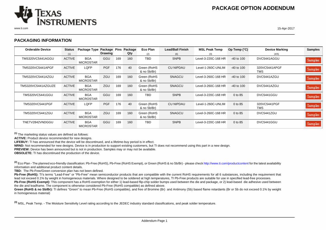
PACKAGE OPTION ADDENDUM
www.ti.com 15-Apr-2017
Addendum-Page 1
PACKAGING INFORMATION
Orderable Device Status(1)
Package Type PackageDrawing
Pins PackageQty
Eco Plan(2)
Lead/Ball Finish(6)
MSL Peak Temp(3)
Op Temp (°C) Device Marking(4/5)
Samples
TMS320VC5441AGGU ACTIVE BGAMICROSTAR
GGU 169 160 TBD SNPB Level-3-220C-168 HR -40 to 100 DVC5441AGGU
TMS320VC5441APGF ACTIVE LQFP PGF 176 40 Green (RoHS& no Sb/Br)
CU NIPDAU Level-1-260C-UNLIM -40 to 100 320VC5441APGFTMS
TMS320VC5441AZGU ACTIVE BGAMICROSTAR
ZGU 169 160 Green (RoHS& no Sb/Br)
SNAGCU Level-3-260C-168 HR -40 to 100 DVC5441AZGU
TMS320VC5441AZGUZE ACTIVE BGAMICROSTAR
ZGU 169 160 Green (RoHS& no Sb/Br)
SNAGCU Level-3-260C-168 HR -40 to 100 DVC5441AZGU
TMS320VC5441GGU ACTIVE BGAMICROSTAR
GGU 169 160 TBD SNPB Level-3-220C-168 HR 0 to 85 DVC5441GGU
TMS320VC5441PGF ACTIVE LQFP PGF 176 40 Green (RoHS& no Sb/Br)
CU NIPDAU Level-1-260C-UNLIM 0 to 85 320VC5441PGFTMS
TMS320VC5441ZGU ACTIVE BGAMICROSTAR
ZGU 169 160 Green (RoHS& no Sb/Br)
SNAGCU Level-3-260C-168 HR 0 to 85 DVC5441ZGU
TNETV2842VNDGGU ACTIVE BGAMICROSTAR
GGU 169 160 TBD SNPB Level-3-220C-168 HR 0 to 85 DVC5441GGU
(1) The marketing status values are defined as follows:ACTIVE: Product device recommended for new designs.LIFEBUY: TI has announced that the device will be discontinued, and a lifetime-buy period is in effect.NRND: Not recommended for new designs. Device is in production to support existing customers, but TI does not recommend using this part in a new design.PREVIEW: Device has been announced but is not in production. Samples may or may not be available.OBSOLETE: TI has discontinued the production of the device.
(2) Eco Plan - The planned eco-friendly classification: Pb-Free (RoHS), Pb-Free (RoHS Exempt), or Green (RoHS & no Sb/Br) - please check http://www.ti.com/productcontent for the latest availabilityinformation and additional product content details.TBD: The Pb-Free/Green conversion plan has not been defined.Pb-Free (RoHS): TI's terms "Lead-Free" or "Pb-Free" mean semiconductor products that are compatible with the current RoHS requirements for all 6 substances, including the requirement thatlead not exceed 0.1% by weight in homogeneous materials. Where designed to be soldered at high temperatures, TI Pb-Free products are suitable for use in specified lead-free processes.Pb-Free (RoHS Exempt): This component has a RoHS exemption for either 1) lead-based flip-chip solder bumps used between the die and package, or 2) lead-based die adhesive used betweenthe die and leadframe. The component is otherwise considered Pb-Free (RoHS compatible) as defined above.Green (RoHS & no Sb/Br): TI defines "Green" to mean Pb-Free (RoHS compatible), and free of Bromine (Br) and Antimony (Sb) based flame retardants (Br or Sb do not exceed 0.1% by weightin homogeneous material)
(3) MSL, Peak Temp. - The Moisture Sensitivity Level rating according to the JEDEC industry standard classifications, and peak solder temperature.
PACKAGE OPTION ADDENDUM
www.ti.com 15-Apr-2017
Addendum-Page 2
(4) There may be additional marking, which relates to the logo, the lot trace code information, or the environmental category on the device.
(5) Multiple Device Markings will be inside parentheses. Only one Device Marking contained in parentheses and separated by a "~" will appear on a device. If a line is indented then it is a continuationof the previous line and the two combined represent the entire Device Marking for that device.
(6) Lead/Ball Finish - Orderable Devices may have multiple material finish options. Finish options are separated by a vertical ruled line. Lead/Ball Finish values may wrap to two lines if the finishvalue exceeds the maximum column width.
Important Information and Disclaimer:The information provided on this page represents TI's knowledge and belief as of the date that it is provided. TI bases its knowledge and belief on informationprovided by third parties, and makes no representation or warranty as to the accuracy of such information. Efforts are underway to better integrate information from third parties. TI has taken andcontinues to take reasonable steps to provide representative and accurate information but may not have conducted destructive testing or chemical analysis on incoming materials and chemicals.TI and TI suppliers consider certain information to be proprietary, and thus CAS numbers and other limited information may not be available for release.
In no event shall TI's liability arising out of such information exceed the total purchase price of the TI part(s) at issue in this document sold by TI to Customer on an annual basis.

MECHANICAL DATA
MPBG157A – AUGUST 2000 – REVISED MAY 2002
1POST OFFICE BOX 655303 • DALLAS, TEXAS 75265
GGU (S–PBGA–N169) PLASTIC BALL GRID ARRAY
0,08 0,10
0,850,95
12,10
11,90SQ
1,40 MAX
0,450,55
0,450,35
Seating Plane
9,60 TYP
G
A
D
BC
EF
HJ
LK
MN
51 32 4 6 7 8 9 10 11 12 13
4073221-3/C 12/01
A1 Corner
0,80
0,80
Bottom View
NOTES: A. All linear dimensions are in millimeters.B. This drawing is subject to change without notice.C. MicroStar BGA configuration
MicroStar BGA is a trademark of Texas Instruments Incorporated.


www.ti.com
PACKAGE OUTLINE
C
176X 0.270.17172X 0.5
PIN 1 ID
(0.13)TYP
0.150.050 -7
4X 21.5
TYP26.225.8
B NOTE 324.223.8
A
NOTE 3
24.223.8
0.750.45
0.25GAGE PLANE
1.6 MAX
(1.4)
PLASTIC QUAD FLATPACK
LQFP - 1.6 mm max heightPGF0176APLASTIC QUAD FLATPACK
4215177/A 05/2017
NOTES: 1. All linear dimensions are in millimeters. Any dimensions in parenthesis are for reference only. Dimensioning and tolerancing per ASME Y14.5M. 2. This drawing is subject to change without notice.3. This dimension does not include mold flash, protrusions, or gate burrs.4. Reference JEDEC registration MS-026.
1
44
45 88
89
132
133176
0.08 C A B
SEE DETAIL A
SEATING PLANE
A 12DETAIL ATYPICAL
0.08 C
SCALE 0.550

www.ti.com
EXAMPLE BOARD LAYOUT
0.05 MAXALL AROUND
0.05 MINALL AROUND
(25.4)
172X (0.5)
176X (1.5)
176X (0.3)
(R0.05) TYP
(25.4)
LQFP - 1.6 mm max heightPGF0176APLASTIC QUAD FLATPACK
4215177/A 05/2017
NOTES: (continued) 5. Publication IPC-7351 may have alternate designs. 6. Solder mask tolerances between and around signal pads can vary based on board fabrication site. 10.
LAND PATTERN EXAMPLEEXPOSED METAL SHOWN
SCALE:4X
SYMM
SYMM
176 133
45 88
89
1321
44
SEE DETAILS
METAL
SOLDER MASKOPENING
NON SOLDER MASKDEFINED SOLDER MASK DETAILS
EXPOSED METAL
SOLDER MASKOPENING
METAL UNDERSOLDER MASK
SOLDER MASKDEFINED
EXPOSED METAL

www.ti.com
EXAMPLE STENCIL DESIGN
172X (0.5)
176X (1.5)
176X (0.3)
(R0.05) TYP
(25.4)
(25.4)
LQFP - 1.6 mm max heightPGF0176APLASTIC QUAD FLATPACK
4215177/A 05/2017
NOTES: (continued) 7. Laser cutting apertures with trapezoidal walls and rounded corners may offer better paste release. IPC-7525 may have alternate design recommendations.8. Board assembly site may have different recommendations for stencil design.
SOLDER PASTE EXAMPLEBASED ON 0.125 mm THICK STENCIL
SCALE:4X
SYMM
SYMM
176 133
45 88
89
1321
44

IMPORTANT NOTICE
Texas Instruments Incorporated (TI) reserves the right to make corrections, enhancements, improvements and other changes to itssemiconductor products and services per JESD46, latest issue, and to discontinue any product or service per JESD48, latest issue. Buyersshould obtain the latest relevant information before placing orders and should verify that such information is current and complete.TI’s published terms of sale for semiconductor products (http://www.ti.com/sc/docs/stdterms.htm) apply to the sale of packaged integratedcircuit products that TI has qualified and released to market. Additional terms may apply to the use or sale of other types of TI products andservices.Reproduction of significant portions of TI information in TI data sheets is permissible only if reproduction is without alteration and isaccompanied by all associated warranties, conditions, limitations, and notices. TI is not responsible or liable for such reproduceddocumentation. Information of third parties may be subject to additional restrictions. Resale of TI products or services with statementsdifferent from or beyond the parameters stated by TI for that product or service voids all express and any implied warranties for theassociated TI product or service and is an unfair and deceptive business practice. TI is not responsible or liable for any such statements.Buyers and others who are developing systems that incorporate TI products (collectively, “Designers”) understand and agree that Designersremain responsible for using their independent analysis, evaluation and judgment in designing their applications and that Designers havefull and exclusive responsibility to assure the safety of Designers' applications and compliance of their applications (and of all TI productsused in or for Designers’ applications) with all applicable regulations, laws and other applicable requirements. Designer represents that, withrespect to their applications, Designer has all the necessary expertise to create and implement safeguards that (1) anticipate dangerousconsequences of failures, (2) monitor failures and their consequences, and (3) lessen the likelihood of failures that might cause harm andtake appropriate actions. Designer agrees that prior to using or distributing any applications that include TI products, Designer willthoroughly test such applications and the functionality of such TI products as used in such applications.TI’s provision of technical, application or other design advice, quality characterization, reliability data or other services or information,including, but not limited to, reference designs and materials relating to evaluation modules, (collectively, “TI Resources”) are intended toassist designers who are developing applications that incorporate TI products; by downloading, accessing or using TI Resources in anyway, Designer (individually or, if Designer is acting on behalf of a company, Designer’s company) agrees to use any particular TI Resourcesolely for this purpose and subject to the terms of this Notice.TI’s provision of TI Resources does not expand or otherwise alter TI’s applicable published warranties or warranty disclaimers for TIproducts, and no additional obligations or liabilities arise from TI providing such TI Resources. TI reserves the right to make corrections,enhancements, improvements and other changes to its TI Resources. TI has not conducted any testing other than that specificallydescribed in the published documentation for a particular TI Resource.Designer is authorized to use, copy and modify any individual TI Resource only in connection with the development of applications thatinclude the TI product(s) identified in such TI Resource. NO OTHER LICENSE, EXPRESS OR IMPLIED, BY ESTOPPEL OR OTHERWISETO ANY OTHER TI INTELLECTUAL PROPERTY RIGHT, AND NO LICENSE TO ANY TECHNOLOGY OR INTELLECTUAL PROPERTYRIGHT OF TI OR ANY THIRD PARTY IS GRANTED HEREIN, including but not limited to any patent right, copyright, mask work right, orother intellectual property right relating to any combination, machine, or process in which TI products or services are used. Informationregarding or referencing third-party products or services does not constitute a license to use such products or services, or a warranty orendorsement thereof. Use of TI Resources may require a license from a third party under the patents or other intellectual property of thethird party, or a license from TI under the patents or other intellectual property of TI.TI RESOURCES ARE PROVIDED “AS IS” AND WITH ALL FAULTS. TI DISCLAIMS ALL OTHER WARRANTIES ORREPRESENTATIONS, EXPRESS OR IMPLIED, REGARDING RESOURCES OR USE THEREOF, INCLUDING BUT NOT LIMITED TOACCURACY OR COMPLETENESS, TITLE, ANY EPIDEMIC FAILURE WARRANTY AND ANY IMPLIED WARRANTIES OFMERCHANTABILITY, FITNESS FOR A PARTICULAR PURPOSE, AND NON-INFRINGEMENT OF ANY THIRD PARTY INTELLECTUALPROPERTY RIGHTS. TI SHALL NOT BE LIABLE FOR AND SHALL NOT DEFEND OR INDEMNIFY DESIGNER AGAINST ANY CLAIM,INCLUDING BUT NOT LIMITED TO ANY INFRINGEMENT CLAIM THAT RELATES TO OR IS BASED ON ANY COMBINATION OFPRODUCTS EVEN IF DESCRIBED IN TI RESOURCES OR OTHERWISE. IN NO EVENT SHALL TI BE LIABLE FOR ANY ACTUAL,DIRECT, SPECIAL, COLLATERAL, INDIRECT, PUNITIVE, INCIDENTAL, CONSEQUENTIAL OR EXEMPLARY DAMAGES INCONNECTION WITH OR ARISING OUT OF TI RESOURCES OR USE THEREOF, AND REGARDLESS OF WHETHER TI HAS BEENADVISED OF THE POSSIBILITY OF SUCH DAMAGES.Unless TI has explicitly designated an individual product as meeting the requirements of a particular industry standard (e.g., ISO/TS 16949and ISO 26262), TI is not responsible for any failure to meet such industry standard requirements.Where TI specifically promotes products as facilitating functional safety or as compliant with industry functional safety standards, suchproducts are intended to help enable customers to design and create their own applications that meet applicable functional safety standardsand requirements. Using products in an application does not by itself establish any safety features in the application. Designers mustensure compliance with safety-related requirements and standards applicable to their applications. Designer may not use any TI products inlife-critical medical equipment unless authorized officers of the parties have executed a special contract specifically governing such use.Life-critical medical equipment is medical equipment where failure of such equipment would cause serious bodily injury or death (e.g., lifesupport, pacemakers, defibrillators, heart pumps, neurostimulators, and implantables). Such equipment includes, without limitation, allmedical devices identified by the U.S. Food and Drug Administration as Class III devices and equivalent classifications outside the U.S.TI may expressly designate certain products as completing a particular qualification (e.g., Q100, Military Grade, or Enhanced Product).Designers agree that it has the necessary expertise to select the product with the appropriate qualification designation for their applicationsand that proper product selection is at Designers’ own risk. Designers are solely responsible for compliance with all legal and regulatoryrequirements in connection with such selection.Designer will fully indemnify TI and its representatives against any damages, costs, losses, and/or liabilities arising out of Designer’s non-compliance with the terms and provisions of this Notice.
Mailing Address: Texas Instruments, Post Office Box 655303, Dallas, Texas 75265Copyright © 2017, Texas Instruments Incorporated