tnb133m ic overvie · 2016-11-09 · confidential 3alogics n-bridge ic overview card emulation nfc...
TRANSCRIPT

Confidential
3alogics
3alogics Inc.
18 – OCT - 2016
( Document : 3AD - SDS - Rev 1.0a )
TNB133M IC Overview
Smart NFC Choice for your Life
Bridge NTM

Confidential
3alogics
■ NFC Introduction
Near field communication (NFC) is a set
of standards for smart-phones and similar
devices to establish radio communication
with each other by touching them together
or bringing them into proximity, usually no
more than a few inches.
• Carrie frequency : 13.56Mz
• Communication method :
Inductive coupling, Magnetic field energy
• Communication Distance (~ 10cm )
: Smart phone ~ 3cm
• Communication Speed
: 106, 212, 424, (848) kpbs
Close communication
Tag(Card) Reader / Writer (Terminal)Multi-standard (ISO/IEC 14443, JIS X 6319-4/Felica, ISO/IEC 15693)
Peer to Peer Communication (Device to Device)NFCIP-1, NFCIP-2 (ISO/IEC 18092, ISO/IEC 21481)
Card Emulation (Secure Element)EMVCo, ISO/IEC 14443, JIS X 6319-4/Felica
What is NFC
- Reader / Writer *Reading Tags
- Peer to Peer *Making Connections
- Card Emulation *Card in a phone
NFC 3 communication mode / 3 Actions
N-Bridge IC Overview
Touch / Tap / Close on

Confidential
3alogics N-Bridge IC Overview
Card Emulation
NFC Forum Type3 Tag (Type F)
Peer to Peer / Data exchange
NFCIP-1, ISO/IEC18092
Passive mode 212kbps or 424kpbs
NFC Device(Smart phone, Dongle, PC ETC)
NFC Target Device / N-bridge System(Consumer electronics, Health care device, ETC)
Target Device peripheral
*Host – NFC Device
*Slave – Target Device
■ What is N-Bridge ? (Action of N-Bridge)
√ N-Bridge Concept : Providing RF interface to RF communicate between NFC Device and Target Device
• Active Type NFC TAG that has Host interface
- SPI / I2C
• Passive Type communication of Load modulation (None RF Generation)
√ N-Bridge Operating mode
• NFC Forum Tag Type3 mode (T3T mode)
• NFC Data Exchange Protocol mode (NFC-DEP mode) / Peer to Peer target
N-
Bridge

Confidential
3alogics
■ N-Bridge Target Application / Target Device
N-Bridge IC Overview
Consumer Electronics Tablet Game
N-Bridge Target Device/Application
STB
Meter
Printer
Business equipment
Health care
deviceHome appliances
ESL/E-paper
Camera/mp 3player
BT Speaker
√ Handover/Making connections
: Bluetooth simple pairing, Wi-Fi
set-up
√ Read/Write the information of
Set device
: Writing and reading information
needed in Target device.
√ System Wake up
: Wake up Sleep mode Target
Device to NFC Host Device like a
Smart phone.
*Target Device (Power save mode)
Confidential
3alogics
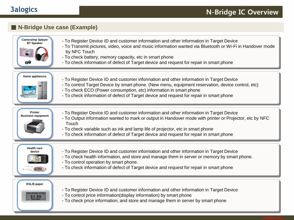
■ N-Bridge Use case (Example)
N-Bridge IC Overview
Printer
Business equipment
Health care
device
Home appliances
- To Register Device ID and customer information and other information in Target Device
- To Transmit pictures, video, voice and music information wanted via Bluetooth or Wi-Fi in Handover mode
by NFC Touch
- To check battery, memory capacity, etc in smart phone
- To check information of defect of Target device and request for repair in smart phone
Camera/mp 3player
BT Speaker
- To Register Device ID and customer information and other information in Target Device
- To control Target Device by smart phone. (New menu, equipment reservation, device control, etc)
- To check ECO (Power consumption, etc) information in smart phone
- To check information of defect of Target device and request for repair in smart phone
- To Register Device ID and customer information and other information in Target Device
- To Output information wanted to mark or output in Handover mode with printer or Projector, etc by NFC
Touch
- To check variable such as ink and lamp life of projector, etc in smart phone
- To check information of defect of Target device and request for repair in smart phone
- To Register Device ID and customer information and other information in Target Device
- To check health information, and store and manage them in server or memory by smart phone.
- To control operation by smart phone.
- To check information of defect of Target device and request for repair in smart phone
- To Register Device ID and customer information and other information in Target Device
- To control price information(display information) by smart phone
- To check price information, and store and manage them in server by smart phone
ESL/E-paper
Confidential
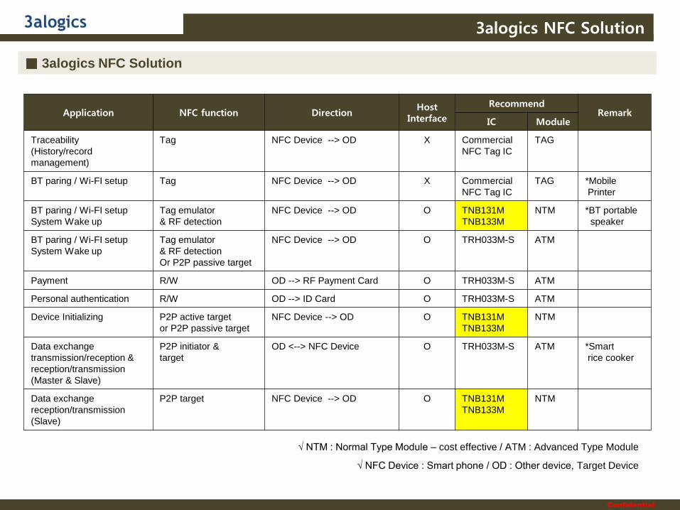
3alogics 3alogics NFC Solution
Application NFC function DirectionHost
Interface
Recommend Remark
IC Module
Traceability
(History/record
management)
Tag NFC Device --> OD X Commercial
NFC Tag IC
TAG
BT paring / Wi-FI setup Tag NFC Device --> OD X Commercial
NFC Tag IC
TAG *Mobile
Printer
BT paring / Wi-FI setup
System Wake up
Tag emulator
& RF detection
NFC Device --> OD O TNB131M
TNB133M
NTM *BT portable
speaker
BT paring / Wi-FI setup
System Wake up
Tag emulator
& RF detection
Or P2P passive target
NFC Device --> OD O TRH033M-S ATM
Payment R/W OD --> RF Payment Card O TRH033M-S ATM
Personal authentication R/W OD --> ID Card O TRH033M-S ATM
Device Initializing P2P active target
or P2P passive target
NFC Device --> OD O TNB131M
TNB133M
NTM
Data exchange
transmission/reception &
reception/transmission
(Master & Slave)
P2P initiator &
target
OD <--> NFC Device O TRH033M-S ATM *Smart
rice cooker
Data exchange
reception/transmission
(Slave)
P2P target NFC Device --> OD O TNB131M
TNB133M
NTM
√ NTM : Normal Type Module – cost effective / ATM : Advanced Type Module
■ 3alogics NFC Solution
√ NFC Device : Smart phone / OD : Other device, Target Device
Confidential
3alogics
■ 3alogics N-Bridge Solution - IC
3alogics NFC Solution
Product Code Package Operating
Temperature
Power supply
(Typ.)
Memory Resonance
Cap.
RF Protocols Host
Interface
TNB131M TQFN16
(3mm X 3mm)
-40 ~ 85°C 1.8V/3.3V 256Byte N-Bridge RAM 23.5pF NFC Type3 I2C/SPI
TNB132M XQFN8
(1.6mm X 1.6mm)
-40 ~ 85°C 3.3V 64Byte N-Bridge RAM
1KByte EEPROM
50pF NFC Type3 I2C
TNB133M QFN16
(4mm X 4mm)
-40 ~ 85°C 1.8V/3.3V Em-MCU(Flip8051)
2KB Xdata RAM
5KByte Code EEPROM
1KB N-Bridge EEPROM
46pF NFC Type3 I2C
UART
TNB134M QFN32
(5mm X 5mm)
-40 ~ 85°C 1.8V/3.3V Em-MCU(8051)
2KB Xdata RAM
15KByte Code EEPROM
1KB N-Bridge EEPROM
23.5pF NFC Type5 I2C
Parametric Table
Target Application
TNB131M / TNB133M
• BT pairing
• Wi-Fi Setup
• ESL
• Consumer electronics
TNB133M
• IoT - NFC Sensor module
TNB134M
• Cold Chain

Confidential
3alogics 3alogics NFC Solution
■ 3alogics N-Bridge Solution – Application (NFC in the IoT)
NFC in the IoT
• 3alogisc NFC Solution
- NFC Bridge IC
- NFC R/W IC
Data Analysis &
Action System
- Wifi-Setup / BT pairing
- AP(gateway) : NFC R/W
IoT device Registration
Confidential
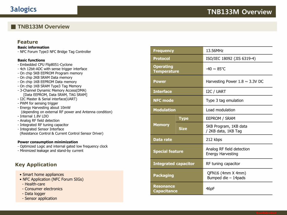
3alogics TNB133M Overview
■ TNB133M Overview
Frequency 13.56MHz
Protocol ISO/IEC 18092 (JIS 6319-4)
OperatingTemperature
-40 ~ 85°C
Power Harvesting Power 1.8 ~ 3.3V DC
Interface I2C / UART
NFC mode Type 3 tag emulation
Modulation Load modulation
Memory
Type EEPROM / SRAM
Size5KB Program, 1KB data / 2KB data, 1KB Tag
Data rate 212 kbps
Special featureAnalog RF field detectionEnergy Harvesting
Integrated capacitor RF tuning capacitor
PackagingQFN16 (4mm X 4mm) Bumped die – 14pads
ResonanceCapacitance
46pF
Key Application
• Smart home appliances• NFC Application (NFC Forum SIGs)
- Health-care- Consumer electronics- Data logger- Sensor application
FeatureBasic information- NFC Forum Type3 NFC Bridge Tag Controller
Basic functions - Embedded CPU Flip8051-Cyclone- 4ch 12bit-ADC with sense trigger interface- On chip 5KB EEPROM Program memory- On chip 2KB SRAM Data memory- On chip 1KB EEPROM Data memory- On chip 1KB SRAM Type3 Tag Memory- 3-Channel Dynamic Memory Access(DMA)
[Data EEPROM, Data SRAM, TAG SRAM]- I2C Master & Serial interface(UART)- PWM for sensing trigger- Energy Harvesting about 10mW
(depending on external RF power and Antenna condition)- Internal 1.8V LDO - Analog RF field detection- Integrated RF tuning capacitor- Integrated Sensor Interface
(Resistance Control & Current Control Sensor Driver)
Power consumption minimization- Optimized Logic and internal gated low frequency clock- Minimized leakage and stand-by current

Confidential
3alogics TNB133M Block Diagram
■ TNB133M Block Diagram
DIGITAL LOGIC
RF interface
Rectifier
MOD/DEMO
POR /
CLK Extractor
Power Management
T3T /
NFC-DEP
Limiter
/ IOSC
I2C Master
/ UART
MEMORY
12B SAR
ADC
EEPROM
6KBytes
SRAM
1K/
2KBytes
ANTP
ANTN
VREC VSS
GP0.0
GP2.3
GP2.2
GP2.0
VDD
Flip8051-
Cyclone
MCU
GP2.1
GP0.2 TESTIRSTGP0.1
SADC3
SADC2
SADC1
SADC0

Confidential
3alogics TNB133M PIN Information
■ TNB133M PIN Information
TNB133M uses 16pin QFN package. (4mm X 4mm)
[ Transparent top view ]
1
2
3
4
5 6 7 8
TNB133ML
16PIN QFN
12
11
10
9
16
15
14
13
GP0.0/CLKIN
GP0.1/TDI/RxD
GP0.2/TMS/TxD
TESTI
GP2.3/SADC3
GP2.2/SADC2
GP2.1/SADC1
GP2.0/SADC0
# Name Dir. Description
1 GP0.0/CLKIN IO GPIO0.0/TEST MCU Clock in
2 GP0.1/TDI/RxD IO GPIO0.1/TEST Data in /UARTRX *Pull-up
3 GP0.2/TMS/TxD IO GPIO0.2/TEST Mode select /UARTTX *Pull-up
4 TESTI I IC TEST Mode select (Active high)
5 VDD PWR 1.8V regulator output / Logic Power & IO Power
6 NC . No Connection
7 NC . No Connection
8 VSS GND Ground
9 GP2.0/SADC0 IOGPIO2.0/ADC input0, with sensing resistor1/I2C
SCL/TNBTest Clk In(0.5 ~ 5.0K)
10 GP2.1/SADC1 IOGPIO2.1/ADC input1, with sensing resistor1/I2C
SDA/TNBTest Data In (0.5 ~ 5.0K)
11 GP2.2/SADC2 IOGPIO2.2/ADC input2, with sensing
resistor2//TNBTest out2 (10 ~ 200K)
12 GP2.3/SADC3 IOGPIO2.3/ADC input3, with sensing
resistor2/UARTTX/TNBTest out1 (10~ 200K)
13 VREC PWR Rectifier output / Harvesting Power
14 ANTN I Antenna negative input
15 ANTP I Antenna positive input
16 RST I IC RESET
TNB133M

Confidential
3alogics
■ TNB133M Package Outline Dimension
Note :
1. All dimensions are In millimeters.
2. Dimensioning and Tolerancing per JEDEC m□-220
Dimensional Ref. Dimensional Tol.REF. min. nom. max. aaa 0.10
A 0.700 0.750 0.800 bbb 0.10
A1 0.000 -- 0.050 ccc 0.10
A3 0.0203 Ref. ddd 0.05
D 3.950 4.000 4.050 eee 0.08
E 3.950 4.000 4.050 fff 0.10
D2 2.400 2.450 2.500
E2 2.400 0.250 0.300
b 0.200 0.250 0.300
L 0.350 0.400 0.450
e 0.500 BSC
K 0.200 MIN
TNB133M POD

Confidential
3alogics TNB133M ET SPEC
■ TNB133M Electrical Characteristics
Symbol Parameter MIN TYP MAX UNIT
Top Operating temperature range -40 +25 +85 ℃
VDD Analog/Digital Core and IO power supply 1.62 1.8 1.98 V
VREC Harvesting Power 1.7 3.0 3.6 V
Symbol Parameter TEST Conditions MIN TYP MAX UNIT
IPWR-3.0V
Power Supply
Current, VCC=3.0V
Active mode, T=25°C
(LDO+IO+RF+VDD Power)- 1.9 - mA
Symbol Parameter MIN TYP MAX UNIT
Vant_pk Antenna input Voltage - - 10 Vpk-pk
VREC_op IC Rectifier Operating Voltage - - 3.6 V
Cin Internal resonance capacitance 41.4 46 50.6 pF
Operating condition range
Current Consumption
RF Interface characteristics
Symbol Parameter MIN TYP MAX UNIT
Amd ASK modulation depth (10%) / downlink - - 30 %
RXsen Rx Sensitivity 40 - - mV
ASK Demodulator characteristics
Symbol Parameter MIN TYP MAX UNIT
VREC Rectifier output voltage -0.5 - 3.6 V
Tstg Storage temperature -55 - 125 °C
VESD Electrostatic discharge voltage - 2 - kV
Limiting characteristics

Confidential
3alogics
■ Integrated Capacitor – Resonance Capacitance
ProductResonant frequency
(MHz)CIC (pF) Cext (pF) Ccon (pF) Cant (pF) Ctotal (pF)
Antenna Coil inductance (μH)
TNB133M
13.3
46 0 1 1 48 2.98
46 0 1 3 50 2.86
46 0 1 5 52 2.75
13.56
46 0 1 1 48 2.87
46 0 1 3 50 2.76
46 0 1 5 52 2.65
13.9
46 0 1 1 48 2.73
46 0 1 3 50 2.62
46 0 1 5 52 2.52
Integrated Capacitor Typ. : 46pF @13.56MHz L = 2.52 ~ 2.98μH
* Recommended Frequency : 13.6 ~ 13.8MHz
TNB133M RES-CAP

Confidential
3alogics
■ TNB133M Sensing IO Architecture
GPIO
(PBCSUDSL8) SEN_RCNT
(3bit)
SEN_ICNT
(6bit i-DAC)
PAD
PADR
Currnet Source BiasCurrent
Source Block
I SENCLK_R SENCLK_I
ADC_Input
(CH0 ~ CH3)
cnt cnt cnt
1.8/3.3V 1.8V 1.8V
TNB133M Sensor Interface (1/4)
Confidential
3alogics
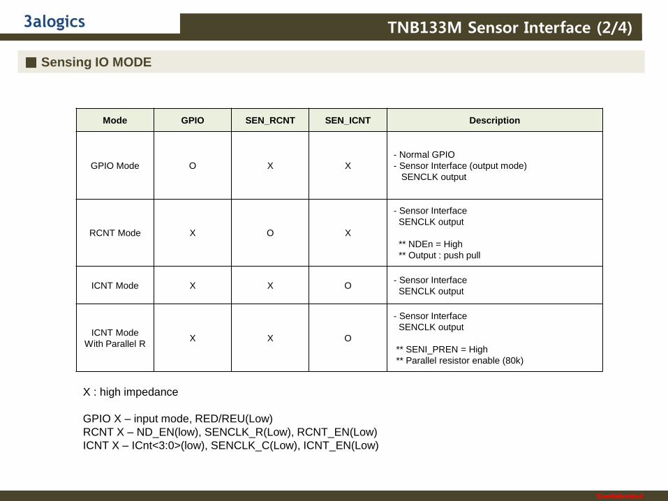
■ Sensing IO MODE
Mode GPIO SEN_RCNT SEN_ICNT Description
GPIO Mode O X X
- Normal GPIO
- Sensor Interface (output mode)
SENCLK output
RCNT Mode X O X
- Sensor Interface
SENCLK output
** NDEn = High
** Output : push pull
ICNT Mode X X O- Sensor Interface
SENCLK output
ICNT Mode
With Parallel RX X O
- Sensor Interface
SENCLK output
** SENI_PREN = High
** Parallel resistor enable (80k)
X : high impedance
GPIO X – input mode, RED/REU(Low)
RCNT X – ND_EN(low), SENCLK_R(Low), RCNT_EN(Low)
ICNT X – ICnt<3:0>(low), SENCLK_C(Low), ICNT_EN(Low)
TNB133M Sensor Interface (2/4)

Confidential
3alogics
■ GPIO – Resistor Control (GP2.0 ~ 2.3)
Name Address Value
SENSRSEL1
(R/W)0xC6
Bit 7-bit 6-bit 5-bit 4-bit 3-bit 2-bit 1-bit 0-bit
Symbol PREnCh1 LRSelCh1 PREnCh0 LRSelCh0
Access RFU r/w r/w r/w RFU r/w r/w r/w
Reset 0 0 0 0 0 0 0 0
Number Name Description
7 PREnCh1 P2.1 Parallel resistor enable (80k)
6:4 LRSelCh1P2.1 Sensing low resistor select
000 – 0.5k, 001 – 1.0k, 010 – 1.5k, 011 – 2.0k, 100 – 2.5k, 101 – 5.0k *Others : Open
3 PREnCh0 P2.0 Parallel resistor enable (80k)
2:0 LRSelCh0P2.0 Sensing low resistor select
000 – 0.5k, 001 – 1.0k, 010 – 1.5k, 011 – 2.0k, 100 – 2.5k, 101 – 5.0k *Others : Open
TNB133M Sensor Interface (3/4)
Name Address Value
SENSRSEL2
(R/W)0xC7
Bit 7-bit 6-bit 5-bit 4-bit 3-bit 2-bit 1-bit 0-bit
Symbol PREnCh3 LRSelCh3 PREnCh2 LRSelCh2
Access RFU r/w r/w r/w RFU r/w r/w r/w
Reset 0 0 0 0 0 0 0 0
Number Name Description
7 PREnCh3 P2.3 Parallel resistor enable (80k)
6:4 LRSelCh3P2.3 Sensing low resistor select
000 – 10k, 001 – 25k, 010 – 50k, 011 – 80k, 100 – 100k, 101 – 200k *Others : Open
3 PREnCh2 P2.2 Parallel resistor enable (80k)
2:0 LRSelCh2P2.2 Sensing low resistor select
000 – 10k, 001 – 25k, 010 – 50k, 011 – 80k, 100 – 100k, 101 – 200k *Others : Open
Confidential
3alogics
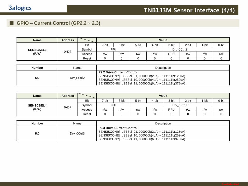
Name Address Value
SENSCSEL3
(R/W)0xDE
Bit 7-bit 6-bit 5-bit 4-bit 3-bit 2-bit 1-bit 0-bit
Symbol RFU Drv_CCtrl2
Access r/w r/w r/w r/w RFU r/w r/w r/w
Reset 0 0 0 0 0 0 0 0
Number Name Description
5:0 Drv_CCtrl2
P2.2 Drive Current Control
SENSISCON의 ILSBSel 01, 000000b(2uA) ~ 111111b(126uA)
SENSISCON의 ILSBSel 10, 000000b(4uA) ~ 111111b(252uA)
SENSISCON의 ILSBSel 11, 000000b(6uA) ~ 111111b(378uA)
■ GPIO – Current Control (GP2.2 ~ 2.3)
TNB133M Sensor Interface (4/4)
Name Address Value
SENSCSEL4
(R/W)0xDF
Bit 7-bit 6-bit 5-bit 4-bit 3-bit 2-bit 1-bit 0-bit
Symbol RFU Drv_CCtrl3
Access r/w r/w r/w r/w RFU r/w r/w r/w
Reset 0 0 0 0 0 0 0 0
Number Name Description
5:0 Drv_CCtrl3
P2.3 Drive Current Control
SENSISCON의 ILSBSel 01, 000000b(2uA) ~ 111111b(126uA)
SENSISCON의 ILSBSel 10, 000000b(4uA) ~ 111111b(252uA)
SENSISCON의 ILSBSel 11, 000000b(6uA) ~ 111111b(378uA)
Confidential
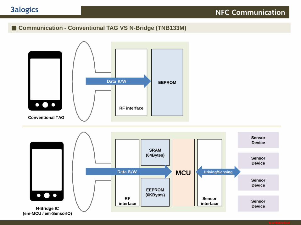
3alogics NFC Communication
■ Communication - Conventional TAG VS N-Bridge (TNB133M)
RF
interface
SRAM
(64Bytes)
EEPROM
(6KBytes)Sensor
interface
Sensor
Device
Data R/W
RF interface
EEPROMData R/W
Conventional TAG
N-Bridge IC
(em-MCU / em-SensorIO)
MCU Driving/Sensing
Sensor
Device
Sensor
Device
Sensor
Device
Confidential
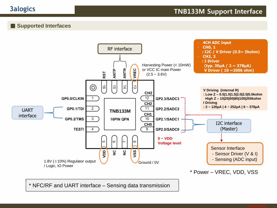
3alogics TNB133M Support Interface
■ Supported Interfaces
* Power – VREC, VDD, VSS
UART interface
I2C interface(Master)
RF interface
Harvesting Power (< 10mW)
or VCC IC main Power
(2.5 ~ 3.6V)
Ground / 0V1.8V (±10%) Regulator output
/ Logic, IO Power
0 ~ VDD
Voltage level
Sensor Interface
- Sensor Driver (V & I)
- Sensing (ADC input)
V Driving (internal R)
: Low Z – 0.5|1.0|1.5|2.0|2.5|5.0kohm
High Z – 10|25|50|80|100|200kohm
I Driving
: 2 ~ 126µA | 4 ~ 252µA | 6 ~ 378µA
* NFC/RF and UART interface – Sensing data transmission
- 4CH ADC input- CH0, 1
: I2C / V Driver (0.5~ 5kohm) - CH2, 3
: I Driver (typ. 30μA / 2 ~ 378μA) V Driver ( 10 ~200k ohm)
CH0
CH1
CH2
CH2
TNB133M
Confidential
3alogics
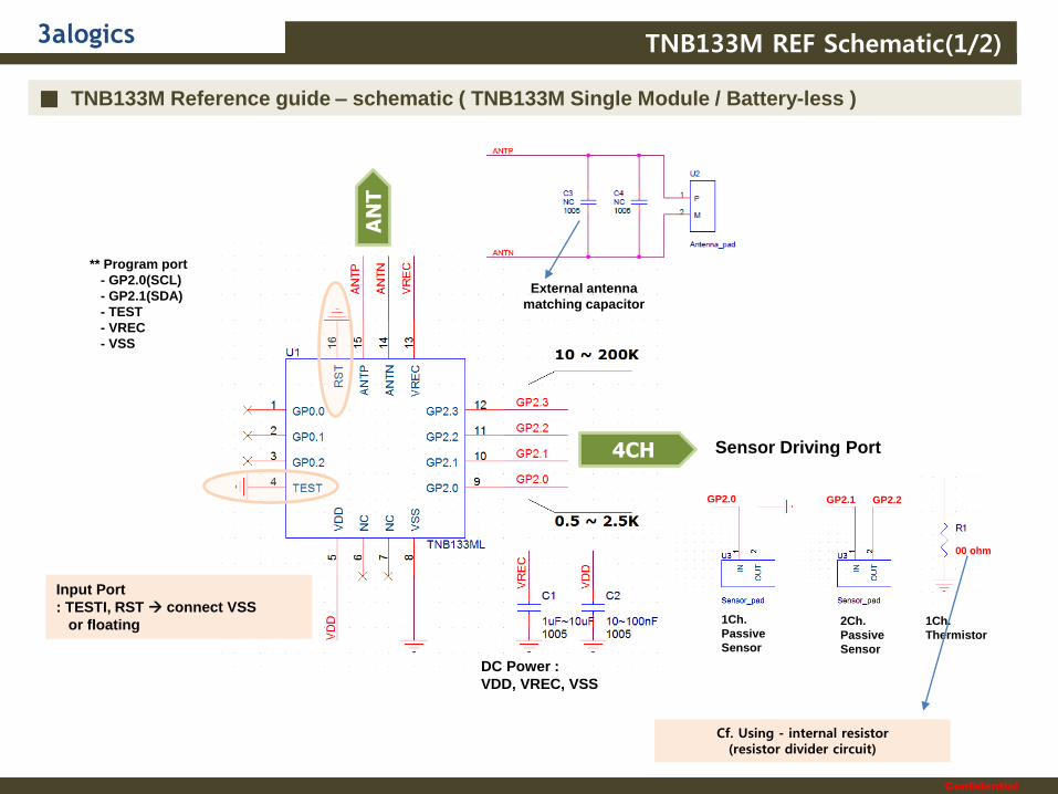
■ TNB133M Reference guide – schematic ( TNB133M Single Module / Battery-less )
4CH Sensor Driving Port
AN
T
DC Power :
VDD, VREC, VSS
Input Port
: TESTI, RST connect VSS
or floating
** Program port
- GP2.0(SCL)
- GP2.1(SDA)
- TEST
- VREC
- VSS
External antenna
matching capacitor
1Ch.
Passive
Sensor
2Ch.
Passive
Sensor
GP2.0 GP2.1 GP2.2
1Ch.
Thermistor
00 ohm
Cf. Using - internal resistor(resistor divider circuit)
TNB133M REF Schematic(1/2)

Confidential
3alogics TNB133M REF Schematic(2/2)
■ TNB133M EVKIT – NBK-300IS Schematic

Confidential
3alogics
www.3alogics.com
Disclaimer3alogics shall not be liable for the incidental or consequential losses of damage to tangible property andinjury in connection with the use of this device. Although the examples in this guide have been testedwith care, they may contain errors and they are not guaranteed for any particular purpose. 3alogicsreserves rights to change any contents to this documents at anytime without any prior notice.
Contact3alogics Inc. 7th Floor, Hyundai-office Bldg.,3, Hwangsaeul-ro 240beon-gil,Bundang-gu, Seongnam-si, Gyeonggi-do, Korea 13595TEL : (82)-(31)-715-7117FAX : (82)-(31)-719-7551E-mail : [email protected]: http://www.3alogics.com
Printed in the Republic of Korea.
IT’s NFC
Smart NFC Choice for your life