topological order in electronic wavefunctions - …topological order in electronic wavefunctions ......
TRANSCRIPT

. . . . . .
Topological Order in Electronic Wavefunctions
Raffaele Resta
Dipartimento di Fisica Teorica, Università di Trieste,and DEMOCRITOS National Simulation Center, IOM-CNR, Trieste
ES12, Wake Forest University, June 2012
. . . . . .
Outline
1 What topology is about
2 Elements of Berryology
3 Chern insulators
4 Noncrystalline insulators
5 Chern number as a cumulant moment in r space
6 Conclusions
. . . . . .
Outline
1 What topology is about
2 Elements of Berryology
3 Chern insulators
4 Noncrystalline insulators
5 Chern number as a cumulant moment in r space
6 Conclusions

. . . . . .
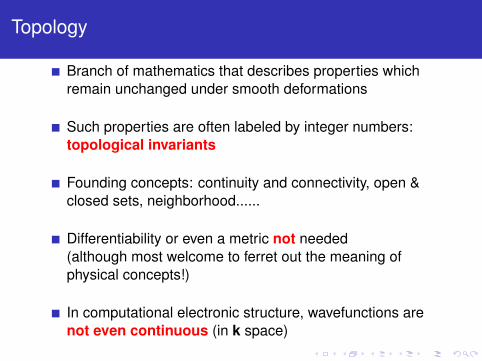
Topology
Branch of mathematics that describes properties whichremain unchanged under smooth deformations
Such properties are often labeled by integer numbers:topological invariants
Founding concepts: continuity and connectivity, open &closed sets, neighborhood......
Differentiability or even a metric not needed(although most welcome to ferret out the meaning ofphysical concepts!)
In computational electronic structure, wavefunctions arenot even continuous (in k space)
. . . . . .
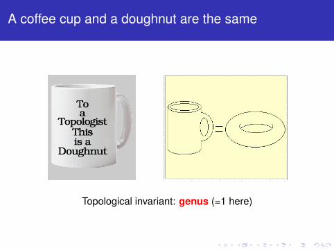
A coffee cup and a doughnut are the same
2/3/12 12:05 PMMath mugs Math humor Mathematician jokes Math mug Math mugs Math gift Math gifts
Page 4 of 6http://mathematicianspictures.com/Math_Mugs_p01.htm
ArchimedesEukleides (Euclid)
DescartesFermatPascal
NewtonLeibniz
EulerLagrange
LaplaceGauss
Ada Byron, LadyLovelaceRiemann
Cantor
Authors PicturesLeonardo Da Vinci
ShopComposers PostersComposers T shirtsFamous Physicists
Math Mug:Certified Math Geek.
Math Mug (set theory):If you consider the set of all sets that havenever been considered ....
Math Mug - TopologyTo a Topologist This is a Doughnut
Math Mug:Real Life is a Special Case(black background)
Topological ClassificationObjects with holes can be classified topologically asfollows:
No holes Genus 0
One hole Genus 1
Two holes Genus 2
Three holes Genus 3
EXAMPLES
The above shapes are topologically equivalentand are of Genus 0
Properties of Space
http://cosmology.uwinnipeg.ca/Cosmology/Properties-of-Space.htm (7 of 11) [03/01/2002 7:23:17 PM]
Topological invariant: genus (=1 here)
. . . . . .
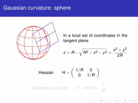
Gaussian curvature: sphere
In a local set of coordinates in thetangent plane
z = R −√
R2 − x2 − y2 ≃ x2 + y2
2R
Hessian H =
(1/R 0
0 1/R
)
Gaussian curvature K = det H =1
R2
. . . . . .
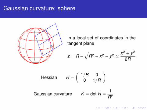
Gaussian curvature: sphere
In a local set of coordinates in thetangent plane
z = R −√
R2 − x2 − y2 ≃ x2 + y2
2R
Hessian H =
(1/R 0
0 1/R
)
Gaussian curvature K = det H =1
R2
. . . . . .
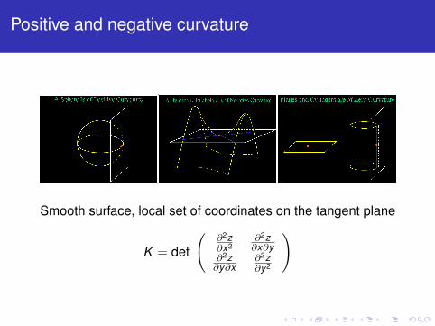
Positive and negative curvature
2/3/12 4:27 PMBob Gardner's "Relativity and Black Holes" Special Relativity
Page 6 of 9http://www.etsu.edu/physics/plntrm/relat/curv.htm
>For example, a plane tangent to a sphere lies entirely on one side of the sphere, and so a sphere is of positivecurvature. In fact, a sphere of radius r is of curvature 1/r2.
A saddle shaped surface (or more precisely, a hyperbolic paraboloid) is of negative curvature. A tangentplane lies on both sides of the surface. Here, the point of tangency is red and the points of intersection areblue. Pringles potato chips are familiar examples of sections of a hyperbolic paraboloid.
2/3/12 4:27 PMBob Gardner's "Relativity and Black Holes" Special Relativity
Page 7 of 9http://www.etsu.edu/physics/plntrm/relat/curv.htm
A cylinder is of zero curvature since a tangent plane lies on one side of the cylinder and the points ofintersection (here in blue) are a line containing the point of tangency. Also, of course, a plane is of zerocurvature.
If two surfaces have the same curvature, we can smoothly transform one into the other without changingdistances (the transformation is called an isometry). For example, a sheet of paper (used here to represent acurvature zero plane) can be rolled up to form a cylinder (which also has zero curvature). However, wecannot role the paper smoothly into a sphere (which is of positive curvature). For example, if we try togiftwrap a basketball, then the paper will overlap itself and have to be crumpled. We also cannot role thepaper smoothly over a saddle shaped surface (which is of negative curvature) since this would require rippingthe paper.
The curvature of a surface is also related to the geometry of the surface.
Smooth surface, local set of coordinates on the tangent plane
K = det
(∂2z∂x2
∂2z∂x∂y
∂2z∂y∂x
∂2z∂y2
)
. . . . . .
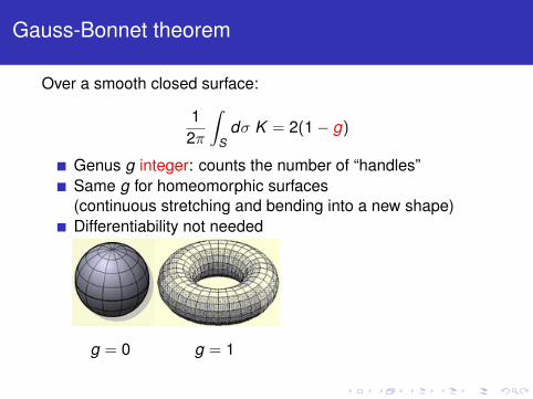
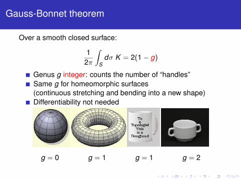
Gauss-Bonnet theorem
Over a smooth closed surface:
12π
∫S
dσ K = 2(1 − g)
Genus g integer: counts the number of “handles”Same g for homeomorphic surfaces(continuous stretching and bending into a new shape)Differentiability not needed
2/3/12 5:21 PMLotsa 'Splainin' 2 Do: Are all mathematicians crazy?
Page 2 of 8http://lotsasplainin.blogspot.com/2007/11/are-all-mathematicians-crazy.html
Here comes the crazy part. Solving the Poincaré Conjecture comes with a prize
of... $1,000,000! (Put your pinky finger to your mouth like Dr. Evil if you feel so
inclined.)
Grisha doesn't want it.
Separate from that cash, Grisha has been awarded the Fields Medal, equivalent
to the Nobel Prize in math, which also comes with a nice clump of cash. (There
is no Nobel Prize in math.)
Grisha doesn't want it.
Maybe his mama could talk some sense into this boy. But taking a look at this
Rasputin lookin' mofo, if she could talk sense into him, she'd probably start by
not dressin' him funny anymore.
Matty Boy, can you 'splain the Poincaré Conjecture to your gentle readers,
some of whom have serious issues with the math?
Let's give it a shot.
In the picture above, we have three different objects, a sphere, a torus and a
Klein bottle. We are going to consider only the surface of each, which we can
think of as a two dimensional thing in a three dimensional world.
The sphere is the easiest of these. It splits the three dimensional world into
three parts: the inside of the sphere, (known as a ball), the skin of the sphere
and the outside.
A torus is the next easiest. There is an inside, the skin and the outside, but
there's the "hole in the middle", which makes a torus different from a sphere in
mathematically important ways.
Then we have the physically impossible model that is the Klein bottle. It can be
Nyan Newt and Beyond!3 days ago
Oliver WillisEqual Polarization, My Ass6 days ago
Karla McLarenOur online course is here:Emotional Flow!1 week ago
beginning to birdSEOW!2 weeks ago
Geometric DecorationsGeometric decoration #16:Mounted Sierpinski's Gasket4 weeks ago
The Ghost-Grey CatTuesday Football: Well, it's astart4 weeks ago
...other dreamsCourt okays Bush's telecomspying4 weeks ago
It's News 2 Them™Shutting down the gossip blog.1 month ago
The Middle AmericanParty (MAP)2 months ago
trinket999's Looking-GlassWorldOff With His Clothes!2 months ago
There Will Be BreadWhere Are You?3 months ago
distributorcap NYHow To Succeed In PoliticsWithout Really Trying4 months ago
Hug The UndersquidA mega giantess dream5 months ago
Claire DaltonPak/(parenthetical)Not from Concentrate7 months ago
Books 4 GrandchildrenGoodbye8 months ago
When Will I Use This?Finally, I Know When I Will
2/3/12 12:05 PMMath mugs Math humor Mathematician jokes Math mug Math mugs Math gift Math gifts
Page 4 of 6http://mathematicianspictures.com/Math_Mugs_p01.htm
ArchimedesEukleides (Euclid)
DescartesFermatPascal
NewtonLeibniz
EulerLagrange
LaplaceGauss
Ada Byron, LadyLovelaceRiemann
Cantor
Authors PicturesLeonardo Da Vinci
ShopComposers PostersComposers T shirtsFamous Physicists
Math Mug:Certified Math Geek.
Math Mug (set theory):If you consider the set of all sets that havenever been considered ....
Math Mug - TopologyTo a Topologist This is a Doughnut
Math Mug:Real Life is a Special Case(black background)
2/4/12 2:56 PMParty Home Rent - Verhuur van materiaal voor feesten en evenemente…ocation de matériel pour vos fêtes et événements — Party Home Rent
Page 1 of 1http://www.partyhomerent.be/shopping_cart.php?language=fr&sort=2a
Rechercher
Recherche avancée
Appareils de cuisine à gaz (8)
Appareils dessert et accessoires (10)
Lounge (11)
Matériel de table (9)
Assiettes et porcelaine divers (19)
Couverts (20)
Verres (19)
Matériel buffet (16)
Tables et chaises (14)
Etales d'animation équipés (2)
Accessoires (32)
Fournitures café (9)
Frais de livraison (5)
Buffets roulants à bièrre/frigo (9)
Accessoires apéro (23)
Matériel de cuisine (8)
Appareils de cuisine électrics (13)
Linge de table & chaise (32)
Chapiteaux et chauffages (9)
2 Débordeurs Elégance avec 1corde noire ou bordeaux
14,00EUR
14,00EUR
Qu'y-a-t-il dans mon panier ?Enlever Produit(s) Qté. Total
Lubiana tassepotage-consomméblanche 32 cl
1 0,22EUR
Sous-total : 0,22EUR
Copyright 2010 Party Home Rent — Location de matériel pour vos fêtes et événements
1
g = 0 g = 1
g = 1 g = 2
. . . . . .
Gauss-Bonnet theorem
Over a smooth closed surface:
12π
∫S
dσ K = 2(1 − g)
Genus g integer: counts the number of “handles”Same g for homeomorphic surfaces(continuous stretching and bending into a new shape)Differentiability not needed
2/3/12 5:21 PMLotsa 'Splainin' 2 Do: Are all mathematicians crazy?
Page 2 of 8http://lotsasplainin.blogspot.com/2007/11/are-all-mathematicians-crazy.html
Here comes the crazy part. Solving the Poincaré Conjecture comes with a prize
of... $1,000,000! (Put your pinky finger to your mouth like Dr. Evil if you feel so
inclined.)
Grisha doesn't want it.
Separate from that cash, Grisha has been awarded the Fields Medal, equivalent
to the Nobel Prize in math, which also comes with a nice clump of cash. (There
is no Nobel Prize in math.)
Grisha doesn't want it.
Maybe his mama could talk some sense into this boy. But taking a look at this
Rasputin lookin' mofo, if she could talk sense into him, she'd probably start by
not dressin' him funny anymore.
Matty Boy, can you 'splain the Poincaré Conjecture to your gentle readers,
some of whom have serious issues with the math?
Let's give it a shot.
In the picture above, we have three different objects, a sphere, a torus and a
Klein bottle. We are going to consider only the surface of each, which we can
think of as a two dimensional thing in a three dimensional world.
The sphere is the easiest of these. It splits the three dimensional world into
three parts: the inside of the sphere, (known as a ball), the skin of the sphere
and the outside.
A torus is the next easiest. There is an inside, the skin and the outside, but
there's the "hole in the middle", which makes a torus different from a sphere in
mathematically important ways.
Then we have the physically impossible model that is the Klein bottle. It can be
Nyan Newt and Beyond!3 days ago
Oliver WillisEqual Polarization, My Ass6 days ago
Karla McLarenOur online course is here:Emotional Flow!1 week ago
beginning to birdSEOW!2 weeks ago
Geometric DecorationsGeometric decoration #16:Mounted Sierpinski's Gasket4 weeks ago
The Ghost-Grey CatTuesday Football: Well, it's astart4 weeks ago
...other dreamsCourt okays Bush's telecomspying4 weeks ago
It's News 2 Them™Shutting down the gossip blog.1 month ago
The Middle AmericanParty (MAP)2 months ago
trinket999's Looking-GlassWorldOff With His Clothes!2 months ago
There Will Be BreadWhere Are You?3 months ago
distributorcap NYHow To Succeed In PoliticsWithout Really Trying4 months ago
Hug The UndersquidA mega giantess dream5 months ago
Claire DaltonPak/(parenthetical)Not from Concentrate7 months ago
Books 4 GrandchildrenGoodbye8 months ago
When Will I Use This?Finally, I Know When I Will
2/3/12 12:05 PMMath mugs Math humor Mathematician jokes Math mug Math mugs Math gift Math gifts
Page 4 of 6http://mathematicianspictures.com/Math_Mugs_p01.htm
ArchimedesEukleides (Euclid)
DescartesFermatPascal
NewtonLeibniz
EulerLagrange
LaplaceGauss
Ada Byron, LadyLovelaceRiemann
Cantor
Authors PicturesLeonardo Da Vinci
ShopComposers PostersComposers T shirtsFamous Physicists
Math Mug:Certified Math Geek.
Math Mug (set theory):If you consider the set of all sets that havenever been considered ....
Math Mug - TopologyTo a Topologist This is a Doughnut
Math Mug:Real Life is a Special Case(black background)
2/4/12 2:56 PMParty Home Rent - Verhuur van materiaal voor feesten en evenemente…ocation de matériel pour vos fêtes et événements — Party Home Rent
Page 1 of 1http://www.partyhomerent.be/shopping_cart.php?language=fr&sort=2a
Rechercher
Recherche avancée
Appareils de cuisine à gaz (8)
Appareils dessert et accessoires (10)
Lounge (11)
Matériel de table (9)
Assiettes et porcelaine divers (19)
Couverts (20)
Verres (19)
Matériel buffet (16)
Tables et chaises (14)
Etales d'animation équipés (2)
Accessoires (32)
Fournitures café (9)
Frais de livraison (5)
Buffets roulants à bièrre/frigo (9)
Accessoires apéro (23)
Matériel de cuisine (8)
Appareils de cuisine électrics (13)
Linge de table & chaise (32)
Chapiteaux et chauffages (9)
2 Débordeurs Elégance avec 1corde noire ou bordeaux
14,00EUR
14,00EUR
Qu'y-a-t-il dans mon panier ?Enlever Produit(s) Qté. Total
Lubiana tassepotage-consomméblanche 32 cl
1 0,22EUR
Sous-total : 0,22EUR
Copyright 2010 Party Home Rent — Location de matériel pour vos fêtes et événements
1
g = 0 g = 1 g = 1 g = 2
. . . . . .
Debut of topology in electronic structure
VOLUME 45, NUMBER 6 PHYSICAL REVIEW LETTERS 11 AUGUST 1/80
invalidate both the relation N =Nz and Eq. (4).However, the experimental results strongly sug-gest that such carriers do not invalidate Eq. (4).At present there is both theoretical and experi-mental investigation of this type of localiza-tion.""" Ando' has suggested that the electronsin impurity bands, arising from short range scat-terers, do not contribute to the Hall current;whereas the electrons in the Landau level giverise to the same Hall current as that obtainedwhen all the electrons are in the level and canmove freely. Clearly this process must be oc-curing but its range of validity must be carefullyexamined as an accompaniment to highly accuratemeasurements of Hall resistance.For high-precision measurements we used a
normal resistance R, in series with the device.The voltage drop, U„across R„and the voltagesUH and Upp across and along the device was meas-ured with a high impedance voltmeter (R &2 x10'0
400
200.
0). The resistance R, was calibrated by the Phys-ikalisch Technische Bundesanstalt, Braunschweig,and had a value of Rp 9999.69 0 at a temperatureof 20'C. A typical result of the measured Hallresistance R„=UH /I =UHR, /U„and the resis-tance, R» =U»R, /U„between the potentialprobes of the device is shown in Fig. 2 (J3 =13 T,T =1.8 K). The minimum in cr„„atV, =23.6 Pcorresponds to the minimum at V~ =8.7 V in Fig.1, because the thicknesses of the gate oxides ofthese two samples differ by a factor of 3.6. Ourexperimental arrangement was not sensitiveenough to measure a value of R» of less than 0.10 which was found in the gate-voltage region23.40 V& V &23.80 V. The Hall resistance in thisgate voltage region had a value of 6453.3+ 0.1 Q.This inaccuracy of + 0.1 0 was due to the limitedsensitivity of the voltmeter. We would like tomention that most of the samples, especially de-vices with a small length-to-width ratio, showeda minimum in the Hall voltage as a function of Vat gate voltage close to the left side of the plateau.In Fig. 2, this minimum is relatively shallow andhas a value of 6452.87 0 at V~ =23.30 V.In order to demonstrate the insensitivity of the
Hall resistance on the geometry of the device,measurements on two samples with a length-to-width ratio of I /W=0. 65 and I/W=25, respective-ly, are plotted in Fig. 3. The gate-voltage scale
23.0 23.5 24.0 24.5=Vg /V
6454.
6400-
6300-
620023.0
8=13.0 TT =1.8 K
23.5 24.0 24.5
z.6453.
(9 6452.
d
6451
h/4e2+~ p—+~)~+K «~~++
ow
/.0IIIII
III
IIIII
I
IIIIII
0I
1
1
I1
IIlIIII1
0IIII
B=13.9 TT =1.8 K
-- ------L=260 pm, W=400pmL=1000pm W=40 pm
=Vg /V
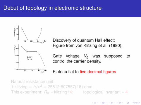
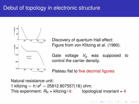
FIG. 2. Hall resistance RH, and device resistance,Rpp, between the potential probes as a function of thegate voltage ~~ in a region of gate voltage correspond-ing to a fully occupied, lowest (n =0) Landau level. Theplateau in RH has a value of 6453.3+ 0.1 Q. The geom-etry of the device was I =400 pm, 8'=50 pm, and L»=130 pm; B=13T.
64500.98 0.99 1.00 101 102
= gate voltage Vg/r'el. units
FIG. 3. Hall resistance RH for two samples with dif-ferent geometry in a gate-voltage region V~ where then =0 Landau level is fully occupied. The recommendedvalue h/4e' is given as 6453.204 &.
496
Discovery of quantum Hall effect:Figure from von Klitzing et al. (1980).
Gate voltage Vg was supposed tocontrol the carrier density.
Plateau flat to five decimal figures
Natural resistance unit:1 klitzing = h/e2 = 25812.807557(18) ohm.This experiment: RH = klitzing / 4: topological invariant = 4
. . . . . .
Debut of topology in electronic structure
VOLUME 45, NUMBER 6 PHYSICAL REVIEW LETTERS 11 AUGUST 1/80
invalidate both the relation N =Nz and Eq. (4).However, the experimental results strongly sug-gest that such carriers do not invalidate Eq. (4).At present there is both theoretical and experi-mental investigation of this type of localiza-tion.""" Ando' has suggested that the electronsin impurity bands, arising from short range scat-terers, do not contribute to the Hall current;whereas the electrons in the Landau level giverise to the same Hall current as that obtainedwhen all the electrons are in the level and canmove freely. Clearly this process must be oc-curing but its range of validity must be carefullyexamined as an accompaniment to highly accuratemeasurements of Hall resistance.For high-precision measurements we used a
normal resistance R, in series with the device.The voltage drop, U„across R„and the voltagesUH and Upp across and along the device was meas-ured with a high impedance voltmeter (R &2 x10'0
400
200.
0). The resistance R, was calibrated by the Phys-ikalisch Technische Bundesanstalt, Braunschweig,and had a value of Rp 9999.69 0 at a temperatureof 20'C. A typical result of the measured Hallresistance R„=UH /I =UHR, /U„and the resis-tance, R» =U»R, /U„between the potentialprobes of the device is shown in Fig. 2 (J3 =13 T,T =1.8 K). The minimum in cr„„atV, =23.6 Pcorresponds to the minimum at V~ =8.7 V in Fig.1, because the thicknesses of the gate oxides ofthese two samples differ by a factor of 3.6. Ourexperimental arrangement was not sensitiveenough to measure a value of R» of less than 0.10 which was found in the gate-voltage region23.40 V& V &23.80 V. The Hall resistance in thisgate voltage region had a value of 6453.3+ 0.1 Q.This inaccuracy of + 0.1 0 was due to the limitedsensitivity of the voltmeter. We would like tomention that most of the samples, especially de-vices with a small length-to-width ratio, showeda minimum in the Hall voltage as a function of Vat gate voltage close to the left side of the plateau.In Fig. 2, this minimum is relatively shallow andhas a value of 6452.87 0 at V~ =23.30 V.In order to demonstrate the insensitivity of the
Hall resistance on the geometry of the device,measurements on two samples with a length-to-width ratio of I /W=0. 65 and I/W=25, respective-ly, are plotted in Fig. 3. The gate-voltage scale
23.0 23.5 24.0 24.5=Vg /V
6454.
6400-
6300-
620023.0
8=13.0 TT =1.8 K
23.5 24.0 24.5
z.6453.
(9 6452.
d
6451
h/4e2+~ p—+~)~+K «~~++
ow
/.0IIIII
III
IIIII
I
IIIIII
0I
1
1
I1
IIlIIII1
0IIII
B=13.9 TT =1.8 K
-- ------L=260 pm, W=400pmL=1000pm W=40 pm
=Vg /V
FIG. 2. Hall resistance RH, and device resistance,Rpp, between the potential probes as a function of thegate voltage ~~ in a region of gate voltage correspond-ing to a fully occupied, lowest (n =0) Landau level. Theplateau in RH has a value of 6453.3+ 0.1 Q. The geom-etry of the device was I =400 pm, 8'=50 pm, and L»=130 pm; B=13T.
64500.98 0.99 1.00 101 102
= gate voltage Vg/r'el. units
FIG. 3. Hall resistance RH for two samples with dif-ferent geometry in a gate-voltage region V~ where then =0 Landau level is fully occupied. The recommendedvalue h/4e' is given as 6453.204 &.
496
Discovery of quantum Hall effect:Figure from von Klitzing et al. (1980).
Gate voltage Vg was supposed tocontrol the carrier density.
Plateau flat to five decimal figures
Natural resistance unit:1 klitzing = h/e2 = 25812.807557(18) ohm.This experiment: RH = klitzing / 4: topological invariant = 4
. . . . . .
Outline
1 What topology is about
2 Elements of Berryology
3 Chern insulators
4 Noncrystalline insulators
5 Chern number as a cumulant moment in r space
6 Conclusions

. . . . . .
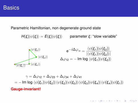
Basics
Parametric Hamiltonian, non degenerate ground state
H(ξ)|ψ(ξ)⟩ = E(ξ)|ψ(ξ)⟩ parameter ξ: “slow variable”
Berry phase: Fundamentals
The Hamiltonian depends on a parameter (and has nondegenerateground eigenstate): H(!)|!(!)! = E(!)|!(!)!.
|!(!1)!
|!(!2)!
|!(!3)!
|!(!4)!
e"i!"
12 =#!(!1)|!(!2)!
|#!(!1)|!(!2)!|
!"12 = " Im log #!(!1)|!(!2)!Berry’s phase — 2010 – p. 7
e−i∆φ12 =⟨ψ(ξ1)|ψ(ξ2)⟩|⟨ψ(ξ1)|ψ(ξ2)⟩|
∆φ12 = − Im log ⟨ψ(ξ1)|ψ(ξ2)⟩
γ = ∆φ12 + ∆φ23 + ∆φ34 + ∆φ41
= − Im log ⟨ψ(ξ1)|ψ(ξ2)⟩⟨ψ(ξ2)|ψ(ξ3)⟩⟨ψ(ξ3)|ψ(ξ4)⟩⟨ψ(ξ4)|ψ(ξ1)⟩
Gauge-invariant!
. . . . . .
Basics
Parametric Hamiltonian, non degenerate ground state
H(ξ)|ψ(ξ)⟩ = E(ξ)|ψ(ξ)⟩ parameter ξ: “slow variable”
|!(!1)!
|!(!2)!
|!(!3)!
|!(!4)!
" = !#12 + !#23 + !#34 + !#41
= " Im log #!(!1)|!(!2)!#!(!2)|!(!3)!#!(!3)|!(!4)!#!(!4)|!(!1)!
Gauge invariant!
Berry’s phase — 2010 – p. 8
e−i∆φ12 =⟨ψ(ξ1)|ψ(ξ2)⟩|⟨ψ(ξ1)|ψ(ξ2)⟩|
∆φ12 = − Im log ⟨ψ(ξ1)|ψ(ξ2)⟩
γ = ∆φ12 + ∆φ23 + ∆φ34 + ∆φ41
= − Im log ⟨ψ(ξ1)|ψ(ξ2)⟩⟨ψ(ξ2)|ψ(ξ3)⟩⟨ψ(ξ3)|ψ(ξ4)⟩⟨ψ(ξ4)|ψ(ξ1)⟩
Gauge-invariant!
. . . . . .
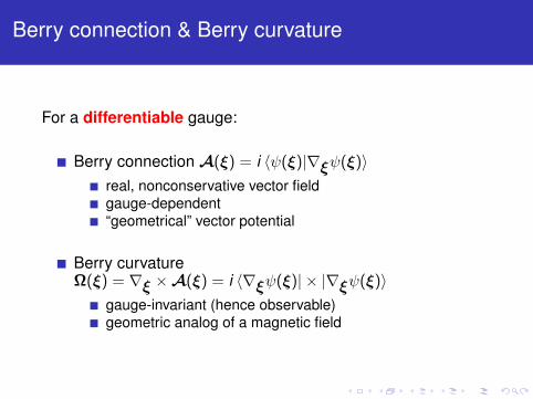
Berry connection & Berry curvature
For a differentiable gauge:
Berry connection A(ξ) = i ⟨ψ(ξ)|∇ξψ(ξ)⟩real, nonconservative vector fieldgauge-dependent“geometrical” vector potential
Berry curvatureΩ(ξ) = ∇ξ × A(ξ) = i ⟨∇ξψ(ξ)| × |∇ξψ(ξ)⟩
gauge-invariant (hence observable)geometric analog of a magnetic field
. . . . . .
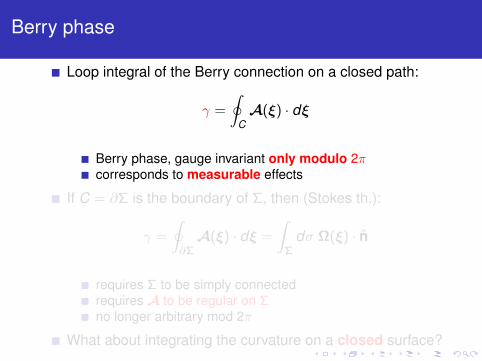
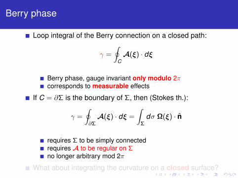
Berry phase
Loop integral of the Berry connection on a closed path:
γ =
∮C
A(ξ) · dξ
Berry phase, gauge invariant only modulo 2πcorresponds to measurable effects
If C = ∂Σ is the boundary of Σ, then (Stokes th.):
γ =
∮∂Σ
A(ξ) · dξ =
∫Σ
dσ Ω(ξ) · n
requires Σ to be simply connectedrequires A to be regular on Σno longer arbitrary mod 2π
What about integrating the curvature on a closed surface?
. . . . . .
Berry phase
Loop integral of the Berry connection on a closed path:
γ =
∮C
A(ξ) · dξ
Berry phase, gauge invariant only modulo 2πcorresponds to measurable effects
If C = ∂Σ is the boundary of Σ, then (Stokes th.):
γ =
∮∂Σ
A(ξ) · dξ =
∫Σ
dσ Ω(ξ) · n
requires Σ to be simply connectedrequires A to be regular on Σno longer arbitrary mod 2π
What about integrating the curvature on a closed surface?
. . . . . .
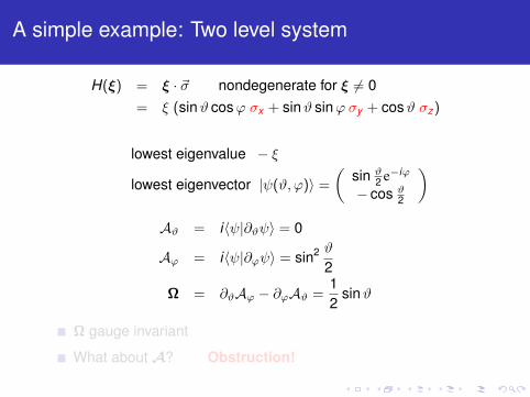
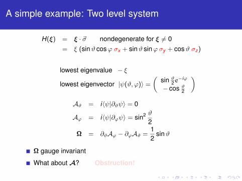
A simple example: Two level system
H(ξ) = ξ · σ nondegenerate for ξ = 0= ξ (sinϑ cosφ σx + sinϑ sinφ σy + cosϑ σz)
lowest eigenvalue − ξ
lowest eigenvector |ψ(ϑ, φ)⟩ =
(sin ϑ
2 e−iφ
− cos ϑ2
)Aϑ = i⟨ψ|∂ϑψ⟩ = 0
Aφ = i⟨ψ|∂φψ⟩ = sin2 ϑ
2
Ω = ∂ϑAφ − ∂φAϑ =12
sinϑ
Ω gauge invariant
What about A? Obstruction!
. . . . . .
A simple example: Two level system
H(ξ) = ξ · σ nondegenerate for ξ = 0= ξ (sinϑ cosφ σx + sinϑ sinφ σy + cosϑ σz)
lowest eigenvalue − ξ
lowest eigenvector |ψ(ϑ, φ)⟩ =
(sin ϑ
2 e−iφ
− cos ϑ2
)Aϑ = i⟨ψ|∂ϑψ⟩ = 0
Aφ = i⟨ψ|∂φψ⟩ = sin2 ϑ
2
Ω = ∂ϑAφ − ∂φAϑ =12
sinϑ
Ω gauge invariant
What about A? Obstruction!
. . . . . .
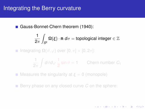
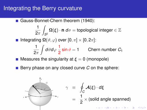
Integrating the Berry curvature
Gauss-Bonnet-Chern theorem (1940):
12π
∫S2
Ω(ξ) · n dσ = topological integer ∈ Z
Integrating Ω(ϑ, φ) over [0, π] × [0,2π]:
12π
∫dϑdφ
12
sinϑ = 1 Chern number C1
Measures the singularity at ξ = 0 (monopole)
Berry phase on any closed curve C on the sphere:

. . . . . .
Integrating the Berry curvature
Gauss-Bonnet-Chern theorem (1940):1
2π
∫S2
Ω(ξ) · n dσ = topological integer ∈ Z
Integrating Ω(ϑ, φ) over [0, π] × [0,2π]:1
2π
∫dϑdφ
12
sinϑ = 1 Chern number C1
Measures the singularity at ξ = 0 (monopole)
Berry phase on any closed curve C on the sphere:
2/5/12 11:58 AMGeometric phases and criticality in spin systems
Page 4 of 12http://rsta.royalsocietypublishing.org/content/364/1849/3463.full
(2.1)
(2.2)
(2.3)
(2.4)
(2.5)
View larger version:In this page In a new windowDownload as PowerPoint Slide
spectrum of eigenvalues,
where |n(λ)〉 and En(λ) are eigenstates and eigenvalues, respectively, of H(λ).
Suppose that the values of λ change slowly along a smooth path in . Underthe adiabatic approximation, a system initially prepared in an eigenstate|n(λ)〉 remains in the corresponding instantaneous eigenspace.
In the simplest case of a non-degenerate eigenvalue, the evolution of theeigenstate is specified by the spectral decomposition (2.1) up to a phasefactor. This phase factor can be evaluated by solving the Schrödinger equationunder the constraint of the adiabatic approximation, yielding
where is the usual dynamical phase, and the extraphase factor is the geometric phase, φ. This phase has the form of a pathintegral of a vector potential A (analogous to the electromagnetical vectorpotential) called the Berry connection, whose components are
As the eigenstates |n(λ)〉 are defined up to an arbitrary phase factor, theBerry connection is not uniquely defined. Nevertheless, when the path integralin expression (2.2) is performed on a closed loop, its value is independent ofthis arbitrary choice, and φ is uniquely defined. Berry was the first to recognizethat the additional phase factor in (2.2) has an inherent geometrical meaning:it cannot be expressed as a single-valued function of λ, but it is a function ofthe path followed by the state during its evolution. Surprisingly, the value ofthis phase depends only on the geometry of the path, and not on the rate atwhich it is traversed. Hence the name ‘geometric phase’.
The simplest, but still significant, example of a geometric phase is the oneobtained for a two-level system, such as a spin-1/2 particle in the presence ofa magnetic field. Its Hamiltonian is given by
where (θ, ϕ) determine the orientation of the magnetic field;
is a SU(2) transformation which rotates theoperator B.σ to the z-direction; and σ=(σx, σy, σz) is the vector of Pauli'soperators, given by
With this parametrization, the Hamiltonian can be represented as a vector on asphere, centred in the point of degeneracy of the Hamiltonian (|B|=0), asshown in figure 1.
Figure 1
The geometric phase isproportional to the solidangle spanned by theHamiltonian with respect toits degeneracy point.
For θ=ϕ=0, we have U= and the two eigenstates of the system given by |+〉
γ ≡∮
CA(ξ) · dξ
=12× (solid angle spanned)

. . . . . .
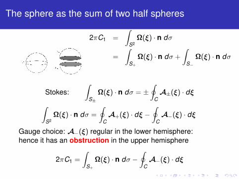
The sphere as the sum of two half spheres
2πC1 =
∫S2
Ω(ξ) · n dσ
=
∫S+
Ω(ξ) · n dσ +
∫S−
Ω(ξ) · n dσ
Stokes:∫
S±
Ω(ξ) · n dσ = ±∮
CA±(ξ) · dξ∫
S2Ω(ξ) · n dσ =
∮C
A+(ξ) · dξ −∮
CA−(ξ) · dξ
Gauge choice: A−(ξ) regular in the lower hemisphere:hence it has an obstruction in the upper hemisphere
2πC1 =
∫S+
Ω(ξ) · n dσ −∮
CA−(ξ) · dξ
. . . . . .
The sphere as the sum of two half spheres
2πC1 =
∫S2
Ω(ξ) · n dσ
=
∫S+
Ω(ξ) · n dσ +
∫S−
Ω(ξ) · n dσ
Stokes:∫
S±
Ω(ξ) · n dσ = ±∮
CA±(ξ) · dξ∫
S2Ω(ξ) · n dσ =
∮C
A+(ξ) · dξ −∮
CA−(ξ) · dξ
Gauge choice: A−(ξ) regular in the lower hemisphere:hence it has an obstruction in the upper hemisphere
2πC1 =
∫S+
Ω(ξ) · n dσ −∮
CA−(ξ) · dξ

. . . . . .
Bloch orbitals (noninteracting electrons in this talk)
Lattice-periodical Hamiltonian (no macroscopic B field);2d, single band, spinless electrons
H|ψk⟩ = εk|ψk⟩Hk|uk⟩ = εk|uk⟩ |uk⟩ = e−ik·r|ψk⟩ Hk = e−ik·rHeik·r
Berry connection and curvature (ξ → k):
A(k) = i⟨uk|∇kuk⟩Ω(k) = i⟨∇kuk| × |∇kuk⟩ = −2 Im ⟨∂kx uk|∂ky uk⟩
BZ (or reciprocal cell) is a closed surface: 2d torusTopological invariant:
C1 =1
2π
∫BZ
dk Ω(k) Chern number
. . . . . .
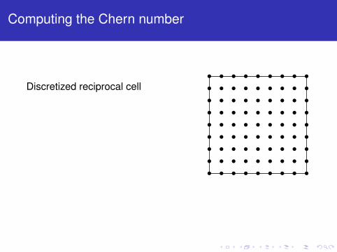
Computing the Chern number
Discretized reciprocal cell

. . . . . .
Computing the Chern number
Discretized reciprocal cell
Periodic gauge choice:where is the obstruction?

. . . . . .
Computing the Chern number
Discretized reciprocal cell
Curvature ≡ Berry phase per unit (reciprocal) areaBerry phase on a small square:
γ = −Im log ⟨uk1 |uk2⟩⟨uk2 |uk3⟩⟨uk3 |uk4⟩⟨uk4 |uk1⟩

. . . . . .
Computing the Chern number
Discretized reciprocal cell
Curvature ≡ Berry phase per unit (reciprocal) areaBerry phase on a small square:
γ = −Im log ⟨uk1 |uk2⟩⟨uk2 |uk3⟩⟨uk3 |uk4⟩⟨uk4 |uk1⟩
Which branch of Im log?

. . . . . .
Computing the Chern number
Discretized reciprocal cell
NonAbelian (many-band):
γ = −Im log det S(k1,k2)S(k2,k3)S(k3,k4)S(k4,k1)
Snn′(ks,ks′) = ⟨unks |unks′⟩
. . . . . .
Outline
1 What topology is about
2 Elements of Berryology
3 Chern insulators
4 Noncrystalline insulators
5 Chern number as a cumulant moment in r space
6 Conclusions
. . . . . .
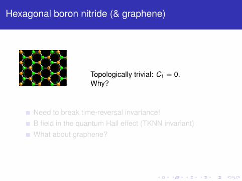
Hexagonal boron nitride (& graphene)
2/5/12 1:06 PMUltrathin hexagonal boron nitride films
Page 1 of 2http://www.physik.unizh.ch/groups/grouposterwalder/kspace/BNhome/BNhome.htm
home
ultrathin hexagonal boron nitride (h-BN)films on metals
Willi Auwärter, Matthias Muntwiler, Martina Corso, Thomas Greberand Jürg Osterwalder
Physics Institute, University of Zurich, 12/12/03
Boron nitrides represent a class of materials with promising properties[1]. They are thermally stable, chemically inert and insulating. Pairs ofboron and nitrogen atoms are isoelectronic to pairs of carbon atoms.Therefore, boron nitrides show a similar structural variety as carbonsolids, including graphitic hexagonalboron nitride (h-BN) and diamond-likecubic boron nitride (c-BN) [2], onion-like fullerenes [3], and multi- andsingle-wall nanotubes [4,5].Differences arise due to thereluctance, in boron nitrides, to form B-B or N-N bonds which excludespentagon formation and thus the synthesis of simple fullerenesanalogous to e.g. C60. In our work we concentrate on hexagonal boronnitride, that is often called "white graphite" due to its color and the layerstructure similar to graphite. The combination of being an electricinsulator and a good thermal conductor that is stable up to hightemperatures and the easy machinability makes h-BN an interestingmaterial for many technical applications. The photograph below showstwo boron nitride blocks. Weaklyphysisorbed layers of h-BN on metalsurfaces have been studied for about adecade [6]. Well-ordered films can begrown by thermal decomposition ofborazine (HBNH)3 on transition metal
surfaces [7]. In most cases studied sofar the film growth was observed to be self-limiting at one monolayer;beyond that the sticking coefficient of the precursor molecule becomesexceedingly small. Most of the work has been concentrated on the
introduction
h-BN on Nickel
h-BN on Rhodium
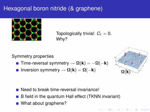
Topologically trivial: C1 = 0.Why?
Need to break time-reversal invariance!B field in the quantum Hall effect (TKNN invariant)What about graphene?
. . . . . .
Hexagonal boron nitride (& graphene)
2/5/12 1:06 PMUltrathin hexagonal boron nitride films
Page 1 of 2http://www.physik.unizh.ch/groups/grouposterwalder/kspace/BNhome/BNhome.htm
home
ultrathin hexagonal boron nitride (h-BN)films on metals
Willi Auwärter, Matthias Muntwiler, Martina Corso, Thomas Greberand Jürg Osterwalder
Physics Institute, University of Zurich, 12/12/03
Boron nitrides represent a class of materials with promising properties[1]. They are thermally stable, chemically inert and insulating. Pairs ofboron and nitrogen atoms are isoelectronic to pairs of carbon atoms.Therefore, boron nitrides show a similar structural variety as carbonsolids, including graphitic hexagonalboron nitride (h-BN) and diamond-likecubic boron nitride (c-BN) [2], onion-like fullerenes [3], and multi- andsingle-wall nanotubes [4,5].Differences arise due to thereluctance, in boron nitrides, to form B-B or N-N bonds which excludespentagon formation and thus the synthesis of simple fullerenesanalogous to e.g. C60. In our work we concentrate on hexagonal boronnitride, that is often called "white graphite" due to its color and the layerstructure similar to graphite. The combination of being an electricinsulator and a good thermal conductor that is stable up to hightemperatures and the easy machinability makes h-BN an interestingmaterial for many technical applications. The photograph below showstwo boron nitride blocks. Weaklyphysisorbed layers of h-BN on metalsurfaces have been studied for about adecade [6]. Well-ordered films can begrown by thermal decomposition ofborazine (HBNH)3 on transition metal
surfaces [7]. In most cases studied sofar the film growth was observed to be self-limiting at one monolayer;beyond that the sticking coefficient of the precursor molecule becomesexceedingly small. Most of the work has been concentrated on the
introduction
h-BN on Nickel
h-BN on Rhodium
Topologically trivial: C1 = 0.Why?
Symmetry propertiesTime-reversal symmetry → Ω(k) = −Ω(−k)
Inversion symmetry → Ω(k) = Ω(−k)
J.N. Fuchs et al.: Topological Berry phase and semiclassical quantization of cyclotron orbits 357
(a)
(b)
Fig. 1. Berry curvature ! (in units of a2) in the conductionband of boron nitride as a function of the Bloch wavevector(kx, ky) (in units of 1/a) in the entire Brillouin zone for "/t =
0.1. The lattice vectors have been taken as a1 =!
32 aex+ 3
2aey ,
a2 = !!
32 aex + 3
2aey. (a) Three dimensional plot (kx, ky , !).(b) Contours of iso-curvature in the Brillouin zone.
symmetry (!(k + G) = !(k)) of the triangular Bravaislattice.
The orbital magnetic moment is easily obtained fromM = e"0! and is shown in Figure 2.
Because of time reversal symmetry, the curvature sat-isfies !(!k) = !!(k) and its integral over the entire BZvanishes. As inversion symmetry is absent !(!k) "= !(k).
The Berry phase for a cyclotron orbit C of constant en-ergy "0 is # (C) = $WC [1! !
|"0| ] where WC # !%!
C d&/2$is the winding number, which is ±1 when encircling a val-ley (because of a vortex in &) and 0 when the orbit isaround the # point, see Figure 3.
(a)
(b)
Fig. 2. Orbital magnetic moment M (in units of e t a2/!) inthe conduction band of boron nitride as a function of the Blochwavevector (kx, ky) (in units of 1/a) in the entire Brillouinzone for "/t = 0.1. (a) Three dimensional plot (kx, ky,M).(b) Contours of iso-M in the Brillouin zone.
A saddle point in the energy dispersion at |"0| =$'2 + t2 separates the cyclotron orbits which encircle the
two valleys from the cyclotron orbit which encircle the #point in the BZ. As a consequence,
# (C) = ! %($[1 !'/|"0|] if ' % |"0| <"'2 + t2
(i.e. WC = !%( = ±1)
= 0 if"'2 + t2 < |"0| %
"'2 + (3t)2
(i.e. WC = 0). (38)
We checked this simple expression for the Berry phasealong a cyclotron orbit numerically by directly comput-ing the integral of the curvature in k space over the areaencircled by the cyclotron orbit.
Ω(k)
Need to break time-reversal invariance!B field in the quantum Hall effect (TKNN invariant)What about graphene?
. . . . . .
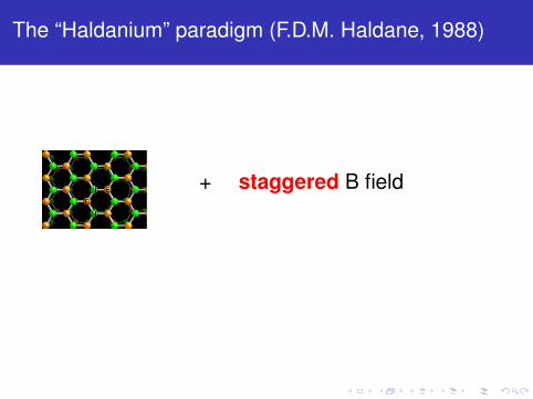
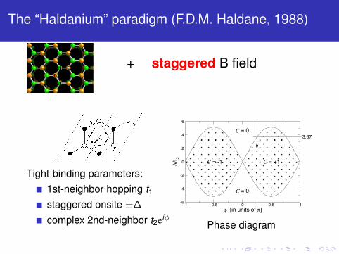
The “Haldanium” paradigm (F.D.M. Haldane, 1988)
2/5/12 1:06 PMUltrathin hexagonal boron nitride films
Page 1 of 2http://www.physik.unizh.ch/groups/grouposterwalder/kspace/BNhome/BNhome.htm
home
ultrathin hexagonal boron nitride (h-BN)films on metals
Willi Auwärter, Matthias Muntwiler, Martina Corso, Thomas Greberand Jürg Osterwalder
Physics Institute, University of Zurich, 12/12/03
Boron nitrides represent a class of materials with promising properties[1]. They are thermally stable, chemically inert and insulating. Pairs ofboron and nitrogen atoms are isoelectronic to pairs of carbon atoms.Therefore, boron nitrides show a similar structural variety as carbonsolids, including graphitic hexagonalboron nitride (h-BN) and diamond-likecubic boron nitride (c-BN) [2], onion-like fullerenes [3], and multi- andsingle-wall nanotubes [4,5].Differences arise due to thereluctance, in boron nitrides, to form B-B or N-N bonds which excludespentagon formation and thus the synthesis of simple fullerenesanalogous to e.g. C60. In our work we concentrate on hexagonal boronnitride, that is often called "white graphite" due to its color and the layerstructure similar to graphite. The combination of being an electricinsulator and a good thermal conductor that is stable up to hightemperatures and the easy machinability makes h-BN an interestingmaterial for many technical applications. The photograph below showstwo boron nitride blocks. Weaklyphysisorbed layers of h-BN on metalsurfaces have been studied for about adecade [6]. Well-ordered films can begrown by thermal decomposition ofborazine (HBNH)3 on transition metal
surfaces [7]. In most cases studied sofar the film growth was observed to be self-limiting at one monolayer;beyond that the sticking coefficient of the precursor molecule becomesexceedingly small. Most of the work has been concentrated on the
introduction
h-BN on Nickel
h-BN on Rhodium
+ staggered B field
. . . . . .
The “Haldanium” paradigm (F.D.M. Haldane, 1988)
2/5/12 1:06 PMUltrathin hexagonal boron nitride films
Page 1 of 2http://www.physik.unizh.ch/groups/grouposterwalder/kspace/BNhome/BNhome.htm
home
ultrathin hexagonal boron nitride (h-BN)films on metals
Willi Auwärter, Matthias Muntwiler, Martina Corso, Thomas Greberand Jürg Osterwalder
Physics Institute, University of Zurich, 12/12/03
Boron nitrides represent a class of materials with promising properties[1]. They are thermally stable, chemically inert and insulating. Pairs ofboron and nitrogen atoms are isoelectronic to pairs of carbon atoms.Therefore, boron nitrides show a similar structural variety as carbonsolids, including graphitic hexagonalboron nitride (h-BN) and diamond-likecubic boron nitride (c-BN) [2], onion-like fullerenes [3], and multi- andsingle-wall nanotubes [4,5].Differences arise due to thereluctance, in boron nitrides, to form B-B or N-N bonds which excludespentagon formation and thus the synthesis of simple fullerenesanalogous to e.g. C60. In our work we concentrate on hexagonal boronnitride, that is often called "white graphite" due to its color and the layerstructure similar to graphite. The combination of being an electricinsulator and a good thermal conductor that is stable up to hightemperatures and the easy machinability makes h-BN an interestingmaterial for many technical applications. The photograph below showstwo boron nitride blocks. Weaklyphysisorbed layers of h-BN on metalsurfaces have been studied for about adecade [6]. Well-ordered films can begrown by thermal decomposition ofborazine (HBNH)3 on transition metal
surfaces [7]. In most cases studied sofar the film growth was observed to be self-limiting at one monolayer;beyond that the sticking coefficient of the precursor molecule becomesexceedingly small. Most of the work has been concentrated on the
introduction
h-BN on Nickel
h-BN on Rhodium
+ staggered B field
f!!"" =1
1 + exp#!" ! !"/#$. !54"
In all subsequent calculations, we set #=0.05 a.u., whichprovides good convergence.
We compute the orbital magnetization as a function of thechemical potential ! with $ fixed at % /3. Using the sameprocedure as in the previous section, we compute the orbitalmagnetization by the means of the heuristic k-space formula!48" and we compare it to the extrapolated value from finitesamples, from L=8 !289 sites" to L=16 !1089 sites". Weverified that a k-point mesh of 100&100 gives well con-verged results for the bulk formula !48".
The orbital magnetization as a function of the chemicalpotential for $=% /3 is shown in Fig. 5. The resulting valuesagree to a good level, and provide solid numerical evidencein favor of Eq. !48", whose analytical proof is still lacking.The orbital magnetization initially increases as the filling ofthe lowest band increases, and rises to a maximum at a !value of about !4.1. Then, as the filling increases, the first!lowest" band crosses the second band and the orbital mag-netization decreases, meaning that the two bands carryopposite-circulating currents giving rise to opposite contribu-tions to the orbital magnetization. The orbital magnetizationremains constant when ! is scanned through the insulatinggap. Upon further increase of the chemical potential, the or-bital magnetization shows a symmetrical behavior as a func-tion of !, the two upper bands having equal but oppositedispersion with respect to the two lowest bands !see Fig. 3".
C. Chern insulating case
In order to check the validity of our heuristic Eq. !48" fora Chern insulator, we switch to the Haldane modelHamiltonian11 that we used in a previous paper7 to addressthe C=0 insulating case. In fact, depending on the parameterchoice, the Chern number C within the model can be eitherzero or nonzero !actually, ±1".
The Haldane model is comprised of a honeycomb latticewith two tight-binding sites per cell with site energies ±',real first-neighbor hoppings t1, and complex second-neighborhoppings t2e±i(, as shown in Fig. 6. The resulting Hamil-
tonian breaks TR symmetry and was proposed !for C= ±1"as a realization of the quantum Hall effect in the absence ofa macroscopic magnetic field. Within this two-band model,one deals with insulators by taking the lowest band as occu-pied.
In our previous paper7 we restricted ourselves to C=0 todemonstrate the validity of Eq. !48", which was also analyti-cally proved. In the present work we address the C!0 insu-lating case, where instead we have no proof of Eq. !48" yet.We are thus performing computer experiments in order toexplore uncharted territory.
Following the notation of Ref. 11, we choose the param-eters '=1, t1=1, and %t2%=1/3. As a function of the fluxparameter $, this system undergoes a transition from zeroChern number to %C%=1 when %sin $%)1/&3.
First we checked the validity of Eq. !48" in the Cherninsulating case by treating the lowest band as occupied. Wecomputed the orbital magnetization as a function of $ by Eq.!48" at a fixed ! value, and we compared it to the magneti-zation of finite samples cut from the bulk. For the periodicsystem, we fix ! in the middle of the gap; for consistency,the finite-size calculations are performed at the same !value, using the Fermi-Dirac distribution of Eq. !54". Thefinite systems have therefore fractional orbital occupancyand a noninteger number of electrons. The biggest samplesize was made up of 20&20 unit cells !800 sites". The com-parison between the finite-size extrapolations and the dis-cretized k-space formula is displayed in Fig. 7. This heuris-tically demonstrates the validity of our main results, Eqs.!46" and !48", in the Chern-insulating case.
Next, we checked the validity of Eq. !48" for the mostgeneral case, following the transition from the metallic phaseto the Chern insulating phase as a function of the chemicalpotential !. To this aim we keep the model Hamiltonianfixed, choosing $=0.7%; for ! in the gap this yields a Cherninsulator. The behavior of the magnetization while ! variesfrom the lowest-band region, to the gap region, and then tothe highest-band region is displayed in Fig. 8, as obtainedfrom both the finite-size extrapolations and the discretizedk-space formula. This shows once more the validity of ourheuristic formula. Also notice that in the gap region the mag-netization is perfectly linear in !, the slope being determinedby the lowest-band Chern number according to Eq. !49".
FIG. 5. Orbital magnetization of the square-lattice model as afunction of the chemical potential ! for $=% /3. The shaded areascorrespond to the two groups of bands. Open circles: extrapolationfrom finite-size samples. Solid line: discretized k-space formula!48".
FIG. 6. Four unit cells of the Haldane model. Filled !open"circles denote sites with E0=!' !+'". Solid lines connecting near-est neighbors indicate a real hopping amplitude t1; dashed arrowspointing to a second-neighbor site indicates a complex hopping am-plitude t2ei$. Arrows indicate sign of the phase $ for second-neighbor hopping.
CERESOLI et al. PHYSICAL REVIEW B 74, 024408 !2006"
024408-10
Tight-binding parameters:1st-neighbor hopping t1staggered onsite ±∆
complex 2nd-neighbor t2eiϕ
approached, the gap at K gets smaller and smaller. Finally,exactly at !! / t2"cr the bands touch at K in such a way that thedispersion relation is linear. Such points are also referred toas Dirac points. When going further into the Chern-insulatorregion, the bands separate again. Note that our specificchoice of t1=1 and t2=1/3 prevents the bands from overlap-ping. If ! and t2 sin " are both chosen to be zero, two Diracpoints form at K and K! and the Haldane model then be-comes an appropriate model for a graphene sheet.20
In the normal-insulator region of the Haldane model theChern number of each band is zero, so that the total Chernnumber !the sum of the Chern numbers of the upper andlower bands" is obviously also zero. When the phase bound-ary is crossed, the Chern numbers of the upper and lowerbands become ±1, but their sum still remains zero. The clo-sure and reopening of the gap as the NI/CI boundary iscrossed corresponds to the “donation” of a Chern unit fromone band to another through the temporarily formed Diracpoint. In the present case, the total Chern number must al-ways remain zero because the model, having a tight-bindingform, assumes Wannier representability of the overall bandspace and a nonzero Chern number is inconsistent with suchan assumption. More generally, the total Chern number of agroup of bands should not change when a gap closure and
reopening occurs among the bands of the group, as long asthe gaps between this group and any lower or higher bandsremains open.
It is possible to argue on very general grounds that a finitesample cut from a Chern insulator must have conductivechannels, otherwise known as chiral edge states, that circu-late around the perimeter of the sample21 in much the sameway as for the quantum Hall effect.22,23 It is therefore ofinterest to investigate the electronic structure of the Haldanemodel from the point of view of the surface band structure.We consider a sample that is finite in the b3 direction !spe-cifically, 30 cells wide" and has periodic boundary conditionsalong the b2 direction #the bi are defined above Eq. !4"$; itsstates can be labeled by a wave vector ky running from !# /ato +# /a, where a is the repeat unit in the y direction. Theenergy eigenvalues are plotted versus ky for several values of! / t2 in Fig. 4. At first sight, the surface band structure showsqualitatively the same information as the bulk band structurein Fig. 3. For ! / t2=6, the valence and conduction bands areseparated by a finite gap. At the Chern transition a Diracpoint forms, showing the characteristic linear dispersion ex-pected around such a point. However, when we go deeperinto the Chern insulator, the surface band structure reveals anew behavior: one surface band now crosses from the lowermanifold to the upper one with increasing ky, and anothercrosses in the opposite direction. Further inspection showsthat the upgoing and downgoing states are localized to theright and left surfaces of the strip, respectively. Thus, if theFermi level lies in the bulk gap, there will be metallic stateswith Fermi velocities parallel to the surfaces and with oppo-site orientation—i.e., a chiral !counterclockwise" circulationof edge states around the perimeter of the sample, as ex-pected.
-1 -0.5 0 0.5 1! [in units of "]
-6
-4
-2
0
2
4
6
#/t 2
= 0
= 0
= -1 = +1
3.67
C
C
C
C
FIG. 2. Chern number of the bottom band of the Haldane modelas a function of the parameters " and ! / t2 !t1=1, t2=1/3". Thevertical line shows the range of parameters that we have chosen forall our calculations.
$ K M K’ $-4
-2
0
2
4
6
ener
gy
6543.6732
FIG. 3. Band structure of the Haldane model along some high-symmetry lines for several values of ! / t2 along the path marked inFig. 2. The inset shows a magnification of the bands at K. Note thatat !! / t2"cr the dispersion is linear.
-20246
ener
gy
-20246
ener
gy
-20246
ener
gy
-"/a $ "/a
#/t2 = 6
(#/t2)cr
#/t2 = 2
FIG. 4. Energy vs wave vector ky for the Haldane model in astrip geometry 30 cells wide along the b3 direction and extendinginfinitely along b2 direction. For ! / t2$ !! / t2"cr !bottom panel",chiral edge states are visible.
INSULATOR/CHERN-INSULATOR TRANSITION IN THE… PHYSICAL REVIEW B 74, 235111 !2006"
235111-3
Phase diagram

. . . . . .
Topological order
a ba b
symmetry as an applied magnetic field would), in simplified models introduced in around 2003 it can lead to a quantum spin Hall effect, in which electrons with opposite spin angular momentum (commonly called spin up and spin down) move in opposite directions around the edge of the droplet in the absence of an external magnetic field2 (Fig. 2b). These simplified models were the first steps towards understanding topological insulators. But it was unclear how realistic the models were: in real materials, there is mixing of spin-up and spin-down electrons, and there is no conserved spin current. It was also unclear whether the edge state of the droplet in Fig. 2b would survive the addition of even a few impurities.
In 2005, a key theoretical advance was made by Kane and Mele3. They used more realistic models, without a conserved spin current, and showed how some of the physics of the quantum spin Hall effect can survive. They found a new type of topological invariant that could be computed for any 2D material and would allow the prediction of whether the material had a stable edge state. This allowed them to show that, despite the edge not being stable in many previous models, there are realistic 2D materials that would have a stable edge state in the absence of a magnetic field; the resultant 2D state was the first topological insulator to be understood. This non-magnetic insulator has edges that act like perfectly conducting one-dimensional electronic wires at low tempera-tures, similar to those in the quantum Hall effect.
Subsequently, Bernevig, Hughes and Zhang made a theoretical prediction that a 2D topological insulator with quantized charge con-ductance along the edges would be realized in (Hg,Cd)Te quantum wells4. The quantized charge conductance was indeed observed in this system, as a quantum-Hall-like plateau in zero magnetic field, in 2007 (ref. 5). These experiments are similar to those on the quantum Hall effect in that they require, at least so far, low temperature and artificial 2D materials (quantum wells), but they differ in that no magnetic field is needed.
Going 3DThe next important theoretical development, in 2006, was the realization6–8 that even though the quantum Hall effect does not general-ize to a genuinely 3D state, the topological insulator does, in a subtle way. Although a 3D ‘weak’ topological insulator can be formed by layering 2D versions, similar to layered quantum Hall states, the resultant state is not stable to disorder, and its physics is generally similar to that of the 2D state. In weak topological insulators, a dislocation (a line-like defect
in the crystal) will always contain a quantum wire like that at the edge of the quantum spin Hall effect (discussed earlier), which may allow 2D topological insulator physics to be observed in a 3D material9.
There is also, however, a ‘strong’ topological insulator, which has a more subtle relationship to the 2D case; the relationship is that in two dimensions it is possible to connect ordinary insulators and topologi-cal insulators smoothly by breaking time-reversal symmetry7. Such a continuous interpolation can be used to build a 3D band structure that respects time-reversal symmetry, is not layered and is topologically non-trivial. It is this strong topological insulator that has protected metallic surfaces and has been the focus of experimental activity.
Spin–orbit coupling is again required and must mix all components of the spin. In other words, there is no way to obtain the 3D strong topologi-cal insulator from separate spin-up and spin-down electrons, unlike in the 2D case. Although this makes it difficult to picture the bulk physics of the 3D topological insulator (only the strong topological insulator will be discussed from this point), it is simple to picture its metallic surface6.
The unusual planar metal that forms at the surface of topological insulators ‘inherits’ topological properties from the bulk insulator. The simplest manifestation of this bulk–surface connection occurs at a smooth surface, where momentum along the surface remains well defined: each momentum along the surface has only a single spin state at the Fermi level, and the spin direction rotates as the momentum moves around the Fermi surface (Fig. 3). When disorder or impurities are added at the surface, there will be scattering between these surface states but, crucially, the topological properties of the bulk insulator do not allow the metallic surface state to vanish — it cannot become local-ized or gapped. These two theoretical predictions, about the electronic structure of the surface state and the robustness to disorder of its metallic behaviour, have led to a flood of experimental work on 3D topological insulators in the past two years.
Experimental realizationsThe first topological insulator to be discovered was the alloy BixSb1!x, the unusual surface bands of which were mapped in an angle-resolved photoemission spectroscopy (ARPES) experiment10,11. In ARPES exper-iments, a high-energy photon is used to eject an electron from a crystal, and then the surface or bulk electronic structure is determined from an analysis of the momentum of the emitted electron. Although the surface structure of this alloy was found to be complex, this work launched a search for other topological insulators.
Figure 1 | Metallic states are born when a surface unties ‘knotted’ electron wavefunctions.!a, An illustration of topological change and the resultant surface state. The trefoil knot (left) and the simple loop (right) represent different insulating materials: the knot is a topological insulator, and the loop is an ordinary insulator. Because there is no continuous deformation by which one can be converted into the other, there must be a surface where the string is cut, shown as a string with open ends (centre), to pass between the two knots; more formally, the topological invariants cannot remain
defined. If the topological invariants are always defined for an insulator, then the surface must be metallic. b, The simplest example of a knotted 3D electronic band structure (with two bands)35, known to mathematicians as the Hopf map. The full topological structure would also have linked fibres on each ring, in addition to the linking of rings shown here. The knotting in real topological insulators is more complex as these require a minimum of four electronic bands, but the surface structure that appears is relatively simple (Fig. 3).
195
NATURE|Vol 464|11 March 2010 PERSPECTIVE!INSIGHT
194-198 Insight Moore NS.indd 195194-198 Insight Moore NS.indd 195 3/3/10 11:30:563/3/10 11:30:56
© 20 Macmillan Publishers Limited. All rights reserved10
approached, the gap at K gets smaller and smaller. Finally,exactly at !! / t2"cr the bands touch at K in such a way that thedispersion relation is linear. Such points are also referred toas Dirac points. When going further into the Chern-insulatorregion, the bands separate again. Note that our specificchoice of t1=1 and t2=1/3 prevents the bands from overlap-ping. If ! and t2 sin " are both chosen to be zero, two Diracpoints form at K and K! and the Haldane model then be-comes an appropriate model for a graphene sheet.20
In the normal-insulator region of the Haldane model theChern number of each band is zero, so that the total Chernnumber !the sum of the Chern numbers of the upper andlower bands" is obviously also zero. When the phase bound-ary is crossed, the Chern numbers of the upper and lowerbands become ±1, but their sum still remains zero. The clo-sure and reopening of the gap as the NI/CI boundary iscrossed corresponds to the “donation” of a Chern unit fromone band to another through the temporarily formed Diracpoint. In the present case, the total Chern number must al-ways remain zero because the model, having a tight-bindingform, assumes Wannier representability of the overall bandspace and a nonzero Chern number is inconsistent with suchan assumption. More generally, the total Chern number of agroup of bands should not change when a gap closure and
reopening occurs among the bands of the group, as long asthe gaps between this group and any lower or higher bandsremains open.
It is possible to argue on very general grounds that a finitesample cut from a Chern insulator must have conductivechannels, otherwise known as chiral edge states, that circu-late around the perimeter of the sample21 in much the sameway as for the quantum Hall effect.22,23 It is therefore ofinterest to investigate the electronic structure of the Haldanemodel from the point of view of the surface band structure.We consider a sample that is finite in the b3 direction !spe-cifically, 30 cells wide" and has periodic boundary conditionsalong the b2 direction #the bi are defined above Eq. !4"$; itsstates can be labeled by a wave vector ky running from !# /ato +# /a, where a is the repeat unit in the y direction. Theenergy eigenvalues are plotted versus ky for several values of! / t2 in Fig. 4. At first sight, the surface band structure showsqualitatively the same information as the bulk band structurein Fig. 3. For ! / t2=6, the valence and conduction bands areseparated by a finite gap. At the Chern transition a Diracpoint forms, showing the characteristic linear dispersion ex-pected around such a point. However, when we go deeperinto the Chern insulator, the surface band structure reveals anew behavior: one surface band now crosses from the lowermanifold to the upper one with increasing ky, and anothercrosses in the opposite direction. Further inspection showsthat the upgoing and downgoing states are localized to theright and left surfaces of the strip, respectively. Thus, if theFermi level lies in the bulk gap, there will be metallic stateswith Fermi velocities parallel to the surfaces and with oppo-site orientation—i.e., a chiral !counterclockwise" circulationof edge states around the perimeter of the sample, as ex-pected.
-1 -0.5 0 0.5 1! [in units of "]
-6
-4
-2
0
2
4
6
#/t 2
= 0
= 0
= -1 = +1
3.67
C
C
C
C
FIG. 2. Chern number of the bottom band of the Haldane modelas a function of the parameters " and ! / t2 !t1=1, t2=1/3". Thevertical line shows the range of parameters that we have chosen forall our calculations.
$ K M K’ $-4
-2
0
2
4
6
ener
gy
6543.6732
FIG. 3. Band structure of the Haldane model along some high-symmetry lines for several values of ! / t2 along the path marked inFig. 2. The inset shows a magnification of the bands at K. Note thatat !! / t2"cr the dispersion is linear.
-20246
ener
gy
-20246
ener
gy
-20246
ener
gy
-"/a $ "/a
#/t2 = 6
(#/t2)cr
#/t2 = 2
FIG. 4. Energy vs wave vector ky for the Haldane model in astrip geometry 30 cells wide along the b3 direction and extendinginfinitely along b2 direction. For ! / t2$ !! / t2"cr !bottom panel",chiral edge states are visible.
INSULATOR/CHERN-INSULATOR TRANSITION IN THE… PHYSICAL REVIEW B 74, 235111 !2006"
235111-3
Ground state wavefunctions differently “knotted” in k spaceTopological order very robustC1 switched only via a metallic state: “cutting the knot”Displays quantum Hall effect at B = 0
. . . . . .
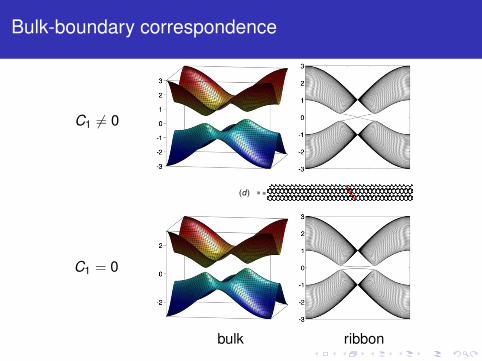
Bulk-boundary correspondence
C1 = 0
C1 = 0
J. Phys. A: Math. Theor. 44 (2011) 113001 Topical Review
(c)(b)(a)
(d )
(g)(e) (f )
Figure 2. (a) The bulk spectrum of Haldane Hamiltonian (equation (1)) (t = 0 and ! = 0.1) asa function of (k1, k2). (b) The energy spectrum of the same Hamiltonian when restricted on aninfinitely long ribbon with open boundary conditions at the two edges. The spectrum is representedas a function of k parallel to the ribbon’s edges. (c) The local density of states (see equation (6)) ofthe ribbon, plotted as an intensity map in the plane of energy (vertical axis) and unit cell numberalong the red line shown in panel (d) (horizontal axis). Blue/red colors correspond to low/highvalues. (d) Illustration of the ribbon used in the calculations shown in panels (b, c) and (f, g). Theribbon was 50 unit cells wide. (e–g) Same as (a–c) but for t = 0.1 and " = 0.
bring major qualitative differences. For some values such as t = 0.1 and ! = 0, the energyspectrum for the ribbon geometry displays an insulating energy gap, while for values liket = 0 and ! = 0.1 it does not. Things become even more intriguing if we look at this spectrumas a function of the momentum parallel to the direction of the ribbon. Examining panels (b)and (f ) of figure 2, we see that when t = 0 and ! = 0.1, the spectrum displays two solitaryenergy bands crossing the bulk insulating gap. For t = 0.1 and ! = 0, we can still see twosolitary bands but they do not cross the bulk insulating gap. If we let the computer run fora while, picking random points in the (t, !) plane, it will slowly reveal that this plane splitsinto regions were the model displays bands that cross the insulating gap like in figure 2(b) andregions where the insulating gap remains open like in figure 2(f ). These regions are shownin figure 3.
It is instructive to also take a look at the maps of the local density of states(LDOS):
#($,n) = 1%
Im(H0 ! $ ! i0+)!1(n,n), (6)
which will reveal the spatial distribution of the quantum states. The #($,n) written abovedepends on three variables, the energy plus the two spatial coordinates, but for a homogeneous
9
bulk ribbon

. . . . . .
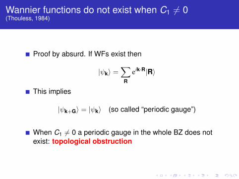
Wannier functions do not exist when C1 = 0(Thouless, 1984)
Proof by absurd. If WFs exist then
|ψk⟩ =∑
R
eik·R|R⟩
This implies
|ψk+G⟩ = |ψk⟩ (so called “periodic gauge”)
When C1 = 0 a periodic gauge in the whole BZ does notexist: topological obstruction
. . . . . .
Wannier functions do not exist when C1 = 0(Thouless, 1984)
Proof by absurd. If WFs exist then
|ψk⟩ =∑
R
eik·R|R⟩
This implies
|ψk+G⟩ = |ψk⟩ (so called “periodic gauge”)
When C1 = 0 a periodic gauge in the whole BZ does notexist: topological obstruction
. . . . . .
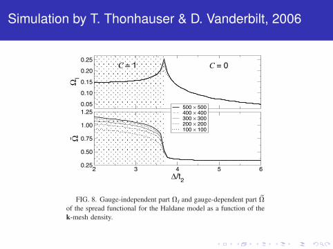
Simulation by T. Thonhauser & D. Vanderbilt, 2006
! = !R!0
"#0"r"R$"2 %15&
are gauge-invariant and gauge-dependent contributions, re-spectively. The gauge-invariant part has been shown to be auseful measure for characterizing the system: !I is finite ininsulators and diverges in metals.9 As for Chern insulators,Resta’s recent argument that !I should remain finite in aquantum Hall fluid26 may hint that this could be the case in acrystalline Chern insulator as well.
MV also gave corresponding k-space expressions for thetwo parts of the functional. Defining the metric tensor g"#
=Re#""uk"Qk""#uk$ where Qk=1! "uk$#uk" %and ""=" /"k"&,these two quantities can be rewritten as
!I =A
%2$&2'BZ
dkTr(g%k&) %16&
and
! =A
%2$&2'BZ
dk"A%k& ! A"2, %17&
where A is the unit cell area, Tr(g)=gxx+gyy, and A is theBZ average of A%k& defined just above Eq. %3&.
In the case of a Chern insulator, the use of the real-spaceexpressions %14& and %15& becomes problematic, since well-localized WF’s cannot be constructed. Nevertheless, thereciprocal-space expressions %16& and %17& remain well de-fined. It is interesting, then, to see how these quantities be-have in a Chern insulator. Do each of these quantities remainfinite, or does one or both of them diverge? Also, what is thebehavior of these quantities as one approaches the NI/CIphase boundary?
To answer these questions, we have computed the quan-tities in Eqs. %16& and %17& using the finite-difference ver-sions of these equations given in Eqs. %34& and %36& of Ref. 7.For the calculation of the gauge-dependent part !, we havefixed our gauge such that "%k$ is real for all k on the lower-energy site in the home unit cell. The results are plotted inFig. 8 for different densities of the k mesh. We confirm that!I is indeed finite inside the Chern-insulator region, as wellas in the normal-insulator region. At the critical value of%& / t2&cr*3.67, however, !I diverges logarithmically withthe number of k points. Furthermore, ! is finite in the nor-mal insulator region, but diverges logarithmically with thenumber of k points for Chern insulators. This latter behavioris consistent with the presence of a vortex in the phases ofthe "wk$ around point ka, which causes A to diverge as "k!ka"!1 and imparts a logarithmic divergence to Eq. %17&. Itfollows that the total spread ! is finite in normal insulatorsand divergent in Chern insulators. Heuristically, it is tempt-ing to associate this divergence with the presence of the me-tallic chiral edge states that are required to exist in Cherninsulators %see Sec. III&, but it is unclear precisely how thesefeatures are related.
VI. DECAY OF THE DENSITY MATRIX
The decay of the density matrix is a fundamental propertyof a system, and it is closely connected to the electron local-ization. It was first studied by Kohn for one-dimensionalinsulators,27 and many others have investigated this topicthereafter.8–10,26,28,29
For periodic samples the density matrix is defined as
'%r,r!& =A
%2$&2 !n=1
occ 'BZ
dk%nk* %r&%nk%r!& , %18&
where we assume that the wave functions %nk are normalizedto one unit cell of area A. If the wave functions are written interms of some basis functions ()
k%r&,
%nk%r& = !)
Cn)k ()
k%r& , %19&
this becomes
'%r,r!& =A
%2$&2 !n=1
occ
!)*'
BZdkCn)
k*Cn*k ()
k*%r&(*k%r!& .
%20&
The Cn)k are the eigenvectors obtained by diagonalizing the
model Hamiltonian—in our case Eq. %4&. In a tight-bindingmodel, the basis functions ()
k%r& are made up of localizedorbitals ( at sites r):
()k%r& = !
Reik·%R+r)&(„r ! %R + r)&… . %21&
Inserting Eq. %21& into Eq. %20& gives
'%r,r!& = !RR!)*
+)*%R! ! R&(*%r ! R ! r)&(%r! ! R! ! r*& ,
%22&
where
0.050.100.150.200.25
!I
2 3 4 5 6"/t2
0.25
0.50
0.75
1.00
1.25
!
500 # 500400 # 400300 # 300200 # 200100 # 100
C C = 0= 1
FIG. 8. Gauge-independent part !I and gauge-dependent part !of the spread functional for the Haldane model as a function of thek-mesh density.
T. THONHAUSER AND DAVID VANDERBILT PHYSICAL REVIEW B 74, 235111 %2006&
235111-6
. . . . . .
Chern insulators
Besides Haldanium (a very popular computationalmaterial), do Chern insulators exist in nature?
Discovery announced at the 2012 APS March Meeting, notconfirmed by any preprint yet (to my knowledge)
Also called QAHE (quantum anomalous Hall effect). Why?
Nonexotic ferromagnetic metals in 3d (Ni, Co, Fe) showAHE: Hall effect in zero B field.Nonquantized: Berry curvature integrated within theFermi volume.

. . . . . .
Time-reversal symmetric topological insulators
In 2d:Kane-Mele model Hamiltonian, 2005A novel invariant, two-valued (Z2)Zero order picture: two copies of the Haldane modelDiscovered: HgxCd1−xTe quantum wells, 2007(L. Molenkamp & al.)
In 3d:Predicted by Fu, Kane, and Mele in 2007Discovered: BixSb1−x , 2008 (M.Z. Hasan & al.)

. . . . . .
2012 O. E. Buckley Condensed Matter Physics Prize
“For the theoretical prediction and experimentalobservation of the quantum spin Hall effect, opening thefield of topological insulators”
Charles L. Kane (U. Pennsylvania)Laurens W. Molenkamp (U. Würzburg, Germany)Shoucheng Zhang (Stanford U.)
Become a Member | Contact Us
Education
International Affairs
Physics for All
Women in Physics
Minorities in Physics
Prizes, Awards & Fellows
Prizes
Awards, Medals & Lectureships
Dissertation Awards
APS Fellows
Other APS Scholarships,Lectureships & Fellowships
Email Print Share
Physicists/Scientists
2012 Oliver E. Buckley Condensed Matter Physics Prize Recipient
Home | Programs | Prizes, Awards and Fellowships | Prizes | Oliver E. Buckley Condensed Matter
Physics Prize
Charles L. Kane University of PennsylvaniaCitation:
"For the theoretical prediction and experimental observation of the quantum spin Halleffect, opening the field of topological insulators."
Background:
Charles Kane received an undergraduate degree in physics from the University ofChicago in 1985 and a Ph.D. in physics from MIT in 1989. After a two year post docat IBM T.J. Watson Research Center he joined the faculty at the University ofPennsylvania, where he is currently Professor of Physics and Astronomy. Professor Kane is known for histheoretical work on the quantum Hall effect, Luttinger liquids and carbon nanotubes. Recently his research hasfocused on the theory of topological phenomena in insulators, superconductors and strongly correlated electronicmaterials. Professor Kane is a Fellow of the American Physical Society and shared the 2010 Europhysics prize,awarded by the European Physical Society.
Selection Committee:
Karin Rabe, Chair; J.M. Phillips; J.C. Campuzano; P.B. Allen; J. Eisenstein
American Physical Society Sites | APS | Journals | PhysicsCentral | Physics
Home | APS Jobs | Media Center | Terms of Use | Site Map
Follow APS:
© 2012 American Physical Society
Become a Member | Contact Us
Education
International Affairs
Physics for All
Women in Physics
Minorities in Physics
Prizes, Awards & Fellows
Prizes
Awards, Medals & Lectureships
Dissertation Awards
APS Fellows
Other APS Scholarships,Lectureships & Fellowships
Email Print Share
Physicists/Scientists
2012 Oliver E. Buckley Condensed Matter Physics Prize Recipient
Home | Programs | Prizes, Awards and Fellowships | Prizes | Oliver E. Buckley Condensed Matter
Physics Prize
Laurens W. Molenkamp University of WuerzburgCitation:
"For the theoretical prediction and experimental observation of the quantum spin Halleffect, opening the field of topological insulators."
Background:
Laurens Molenkamp received undergraduate (1980) and graduate (1985) degrees inPhysical Chemistry from the University of Groningen, the Netherlands, specializing incoherent optical spectroscopy. After completing his PhD, he joined Philips ResearchLaboratories in Eindhoven, the Netherlands, where he soon became involved in quantum transport studies insemiconductor-based nanostructures. This remained his field of interest when he moved back into academia, firstjoining the RWTH in Aachen, Germany, as an associate professor (1994), and subsequently (1999) the Universityof Würzburg, where he holds the Chair of Experimental Physics 3 and leads the II-VI MBE unit. His researchcurrently revolves around quantum transport and semiconductor spintronics, combining nanolithography and lowtemperature transport experiments with the specialized semiconductor epitaxy available at Würzburg. LaurensMolenkamp is a Fellow of the Institute of Physics and the American Physical Society and the recipient of an ERCAdvanced Grant. In 2010, he was a co-recipient of the Europhysics prize, awarded by the Condensed MatterDivision of the European Physical Society.
Selection Committee:
Karin Rabe, Chair; J.M. Phillips; J.C. Campuzano; P.B. Allen; J. Eisenstein
American Physical Society Sites | APS | Journals | PhysicsCentral | Physics
Home | APS Jobs | Media Center | Terms of Use | Site Map
Follow APS:
© 2012 American Physical Society
Become a Member | Contact Us
Education
International Affairs
Physics for All
Women in Physics
Minorities in Physics
Prizes, Awards & Fellows
Prizes
Awards, Medals & Lectureships
Dissertation Awards
APS Fellows
Other APS Scholarships,Lectureships & Fellowships
Email Print Share
Physicists/Scientists
2012 Oliver E. Buckley Condensed Matter Physics Prize Recipient
Home | Programs | Prizes, Awards and Fellowships | Prizes | Oliver E. Buckley Condensed Matter
Physics Prize
Shoucheng Zhang Stanford UniversityCitation:
"For the theoretical prediction and experimental observation of the quantum spin Halleffect, opening the field of topological insulators."
Background:
Shoucheng Zhang is the JG Jackson and CJ Wood professor of physics at StanfordUniversity. He received his BS degree from the Free University of Berlin and in 1983,and his PhD from the State University of New York at Stony Brook in 1987. He was apostdoc fellow at the Institute for Theoretical Physics in Santa Barbara from 1987 to 1989 and a Research StaffMember at the IBM Almaden Research Center from 1989 to 1993. He joined the faculty at Stanford in 1993. He is acondensed matter theorist known for his work on topological insulators, spintronics and high temperaturesuperconductivity. He is a fellow of the American Physical Society and a fellow of the American Academy of Artsand Sciences. He received the Guggenheim fellowship in 2007, the Alexander von Humboldt research prize in 2009and the Europhysics prize in 2010 for his theoretical prediction of the quantum spin Hall effect and topologicalinsulators.
Selection Committee:
Karin Rabe, Chair; J.M Phillips; J.C Campuzano; P.B. Allen; J. Eisenstein
American Physical Society Sites | APS | Journals | PhysicsCentral | Physics
Home | APS Jobs | Media Center | Terms of Use | Site Map
Follow APS:
© 2012 American Physical Society
March MeetingApril MeetingMeeting CalendarAbstract SubmissionArchives of the Bulletin ofthe American PhysicalSocietyPolicies & GuidelinesMeeting PresentationsVirtual Press Rooms
. . . . . .
Outline
1 What topology is about
2 Elements of Berryology
3 Chern insulators
4 Noncrystalline insulators
5 Chern number as a cumulant moment in r space
6 Conclusions
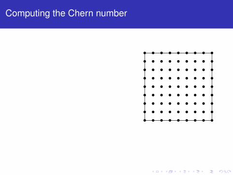
. . . . . .
Computing the Chern number
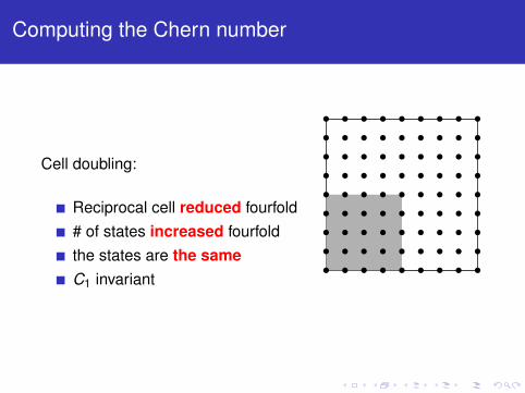
. . . . . .
Computing the Chern number
Cell doubling:
Reciprocal cell reduced fourfold# of states increased fourfoldthe states are the sameC1 invariant
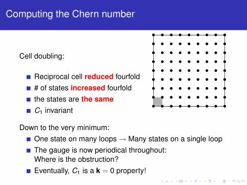
. . . . . .
Computing the Chern number
Cell doubling:
Reciprocal cell reduced fourfold# of states increased fourfoldthe states are the sameC1 invariant
Down to the very minimum:One state on many loops → Many states on a single loopThe gauge is now periodical throughout:Where is the obstruction?Eventually, C1 is a k = 0 property!

. . . . . .
Interpretation of the single point formula
In the large supercell limit
C1 =1
2π
∫BZ
dk Ω(k) → 12π
(2π)2
AcΩ(0)
Chern number → curvature per unit sample area:no integration
Ω(0) is a linear response of the ground state to aninfinitesimal “twist” or “flux” in the many-body Hamiltonian:
H(k) =1
2me
N∑i=1
|pi +ec
A(ri) + ~k|2 + V
Ω(0) = iN∑
n=1
( ⟨∂k1un0|∂k2un0⟩ − ⟨∂k2un0|∂k1un0⟩ )

. . . . . .
Convergence with supercell size(D. Ceresoli & R.R. 2007)
Chern number as a function of thesupercell size, evaluated using thesingle-point formulas for the Haldanemodel Hamiltonian. The largest L cor-responds to 2048 sites in the super-cell.
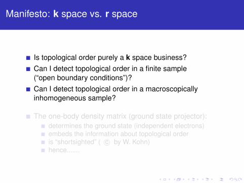
. . . . . .
Manifesto: k space vs. r space
Is topological order purely a k space business?Can I detect topological order in a finite sample(“open boundary conditions”)?Can I detect topological order in a macroscopicallyinhomogeneous sample?
The one-body density matrix (ground state projector):determines the ground state (independent electrons)embeds the information about topological orderis “shortsighted” ( c⃝ by W. Kohn)hence.......
. . . . . .
Outline
1 What topology is about
2 Elements of Berryology
3 Chern insulators
4 Noncrystalline insulators
5 Chern number as a cumulant moment in r space
6 Conclusions
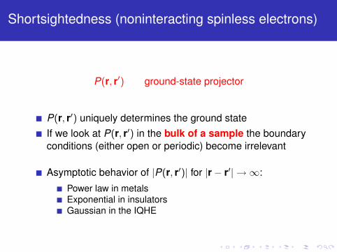
. . . . . .
Shortsightedness (noninteracting spinless electrons)
P(r, r′) ground-state projector
P(r, r′) uniquely determines the ground stateIf we look at P(r, r′) in the bulk of a sample the boundaryconditions (either open or periodic) become irrelevant
Asymptotic behavior of |P(r, r′)| for |r − r′| → ∞:
Power law in metalsExponential in insulatorsGaussian in the IQHE

. . . . . .
Insulating vs. metallic ground stateThe “localization tensor”, a.k.a. second cumulant moment of the electron distribution
Definition within OBCs:
⟨rαrβ⟩c =1
2N
∫drdr′ (r − r′)α(r − r′)β |P(r, r′)|2
Always well defined (r operator harmless within OBCs)Intensive (size-consistent)Real symmetricOriginal theory for correlated wavefunctions
Identical transformation:
Q(r, r′) = δ(r−r′)−P(r, r′) ⟨rαrβ⟩c =1N
Trall spacerαPrβQ
What about the thermodynamic limit?∑α⟨rαrα⟩c diverges in metals∑α⟨rαrα⟩c converges in all insulators:
quantum Hall, band, Chern, Z2, Anderson...... (so far)
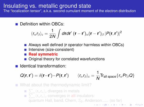
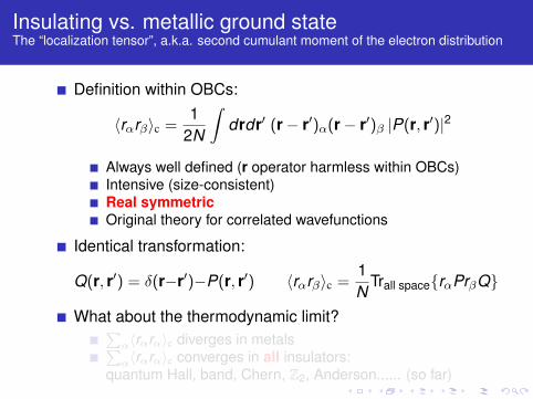
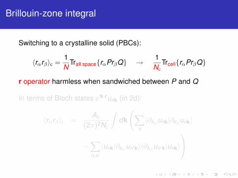
. . . . . .
Brillouin-zone integral
Switching to a crystalline solid (PBCs):
⟨rαrβ⟩c =1N
Trall spacerαPrβQ → 1Nc
TrcellrαPrβQ
r operator harmless when sandwiched between P and Q
In terms of Bloch states eik·runk (in 2d):
⟨rαrβ⟩c =Ac
(2π)2Nc
∫dk
(∑n
⟨∂kαunk|∂kβunk⟩
−∑n,n′
⟨unk|∂kαun′k⟩⟨∂kβun′k|unk⟩
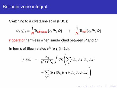
. . . . . .
Brillouin-zone integral
Switching to a crystalline solid (PBCs):
⟨rαrβ⟩c =1N
Trall spacerαPrβQ → 1Nc
TrcellrαPrβQ
r operator harmless when sandwiched between P and Q
In terms of Bloch states eik·runk (in 2d):
⟨rαrβ⟩c =Ac
(2π)2Nc
∫dk
(∑n
⟨∂kαunk|∂kβunk⟩
−∑n,n′
⟨unk|∂kαun′k⟩⟨∂kβun′k|unk⟩

. . . . . .
Marzari-Vanderbilt
∑α
⟨rαrα⟩c =1Nc
ΩI MV gauge-invariant quadratic spread
Naturally endowed with an off-diagonal imaginary part:
Im ⟨r1r2⟩c =Ac
(2π)2NcIm∫
dk∑
n
⟨∂k1unk|∂k2unk⟩
Chern number:
C1 = −1π
Im∫
dk∑
n
⟨∂k1unk|∂k2unk⟩

. . . . . .
Marzari-Vanderbilt
∑α
⟨rαrα⟩c =1Nc
ΩI MV gauge-invariant quadratic spread
Naturally endowed with an off-diagonal imaginary part:
Im ⟨r1r2⟩c =Ac
(2π)2NcIm∫
dk∑
n
⟨∂k1unk|∂k2unk⟩
Chern number:
C1 = −1π
Im∫
dk∑
n
⟨∂k1unk|∂k2unk⟩
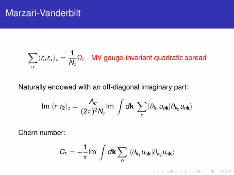
. . . . . .
Marzari-Vanderbilt
∑α
⟨rαrα⟩c =1Nc
ΩI MV gauge-invariant quadratic spread
Naturally endowed with an off-diagonal imaginary part:
Im ⟨r1r2⟩c =Ac
(2π)2NcIm∫
dk∑
n
⟨∂k1unk|∂k2unk⟩
Chern number:
C1 = −1π
Im∫
dk∑
n
⟨∂k1unk|∂k2unk⟩
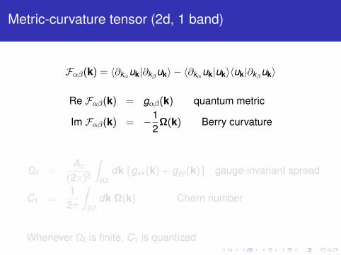
. . . . . .
Metric-curvature tensor (2d, 1 band)
Fαβ(k) = ⟨∂kαuk|∂kβuk⟩ − ⟨∂kαuk|uk⟩⟨uk|∂kβ
uk⟩
Re Fαβ(k) = gαβ(k) quantum metric
Im Fαβ(k) = −12Ω(k) Berry curvature
ΩI =Ac
(2π)2
∫BZ
dk [ gxx(k) + gyy (k) ] gauge-invariant spread
C1 =1
2π
∫BZ
dk Ω(k) Chern number
Whenever ΩI is finite, C1 is quantized
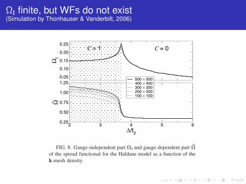
. . . . . .
ΩI finite, but WFs do not exist(Simulation by Thonhauser & Vanderbilt, 2006)
! = !R!0
"#0"r"R$"2 %15&
are gauge-invariant and gauge-dependent contributions, re-spectively. The gauge-invariant part has been shown to be auseful measure for characterizing the system: !I is finite ininsulators and diverges in metals.9 As for Chern insulators,Resta’s recent argument that !I should remain finite in aquantum Hall fluid26 may hint that this could be the case in acrystalline Chern insulator as well.
MV also gave corresponding k-space expressions for thetwo parts of the functional. Defining the metric tensor g"#
=Re#""uk"Qk""#uk$ where Qk=1! "uk$#uk" %and ""=" /"k"&,these two quantities can be rewritten as
!I =A
%2$&2'BZ
dkTr(g%k&) %16&
and
! =A
%2$&2'BZ
dk"A%k& ! A"2, %17&
where A is the unit cell area, Tr(g)=gxx+gyy, and A is theBZ average of A%k& defined just above Eq. %3&.
In the case of a Chern insulator, the use of the real-spaceexpressions %14& and %15& becomes problematic, since well-localized WF’s cannot be constructed. Nevertheless, thereciprocal-space expressions %16& and %17& remain well de-fined. It is interesting, then, to see how these quantities be-have in a Chern insulator. Do each of these quantities remainfinite, or does one or both of them diverge? Also, what is thebehavior of these quantities as one approaches the NI/CIphase boundary?
To answer these questions, we have computed the quan-tities in Eqs. %16& and %17& using the finite-difference ver-sions of these equations given in Eqs. %34& and %36& of Ref. 7.For the calculation of the gauge-dependent part !, we havefixed our gauge such that "%k$ is real for all k on the lower-energy site in the home unit cell. The results are plotted inFig. 8 for different densities of the k mesh. We confirm that!I is indeed finite inside the Chern-insulator region, as wellas in the normal-insulator region. At the critical value of%& / t2&cr*3.67, however, !I diverges logarithmically withthe number of k points. Furthermore, ! is finite in the nor-mal insulator region, but diverges logarithmically with thenumber of k points for Chern insulators. This latter behavioris consistent with the presence of a vortex in the phases ofthe "wk$ around point ka, which causes A to diverge as "k!ka"!1 and imparts a logarithmic divergence to Eq. %17&. Itfollows that the total spread ! is finite in normal insulatorsand divergent in Chern insulators. Heuristically, it is tempt-ing to associate this divergence with the presence of the me-tallic chiral edge states that are required to exist in Cherninsulators %see Sec. III&, but it is unclear precisely how thesefeatures are related.
VI. DECAY OF THE DENSITY MATRIX
The decay of the density matrix is a fundamental propertyof a system, and it is closely connected to the electron local-ization. It was first studied by Kohn for one-dimensionalinsulators,27 and many others have investigated this topicthereafter.8–10,26,28,29
For periodic samples the density matrix is defined as
'%r,r!& =A
%2$&2 !n=1
occ 'BZ
dk%nk* %r&%nk%r!& , %18&
where we assume that the wave functions %nk are normalizedto one unit cell of area A. If the wave functions are written interms of some basis functions ()
k%r&,
%nk%r& = !)
Cn)k ()
k%r& , %19&
this becomes
'%r,r!& =A
%2$&2 !n=1
occ
!)*'
BZdkCn)
k*Cn*k ()
k*%r&(*k%r!& .
%20&
The Cn)k are the eigenvectors obtained by diagonalizing the
model Hamiltonian—in our case Eq. %4&. In a tight-bindingmodel, the basis functions ()
k%r& are made up of localizedorbitals ( at sites r):
()k%r& = !
Reik·%R+r)&(„r ! %R + r)&… . %21&
Inserting Eq. %21& into Eq. %20& gives
'%r,r!& = !RR!)*
+)*%R! ! R&(*%r ! R ! r)&(%r! ! R! ! r*& ,
%22&
where
0.050.100.150.200.25
!I
2 3 4 5 6"/t2
0.25
0.50
0.75
1.00
1.25
!
500 # 500400 # 400300 # 300200 # 200100 # 100
C C = 0= 1
FIG. 8. Gauge-independent part !I and gauge-dependent part !of the spread functional for the Haldane model as a function of thek-mesh density.
T. THONHAUSER AND DAVID VANDERBILT PHYSICAL REVIEW B 74, 235111 %2006&
235111-6
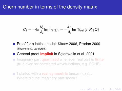
. . . . . .
Chern number in terms of the density matrix
C1 = −4πNc
AcIm ⟨r1r2⟩c = −4π
AcIm Trcellr1Pr2Q
Proof for a lattice model: Kitaev 2006, Prodan 2009(Thanks to D. Vanderbilt)
General proof implicit in Sgiarovello et al. 2001Imaginary part quantized whenever real part is finite(true even for correlated wavefunctions, e.g. FQHE)
I started with a real symmetric tensor ⟨rαrβ⟩c:Where did the imaginary part sneak?
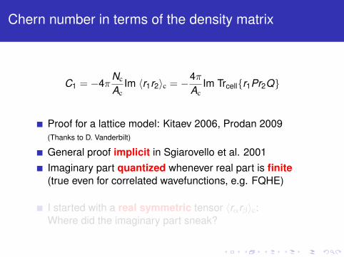
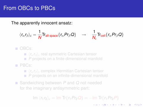
. . . . . .
From OBCs to PBCs
The apparently innocent ansatz:
⟨rαrβ⟩c =1N
Trall spacerαPrβQ → 1Nc
TrcellrαPrβQ
OBCs:⟨rαrβ⟩c real symmetric Cartesian tensorP projects on a finite-dimensional manifold
PBCs:⟨rαrβ⟩c complex Hermitian Cartesian tensorP projects on an infinite-dimensional manifold
Sandwiching between P and Q not neededfor the imaginary antisymmetric part:
Im ⟨r1r2⟩c = Im Trr1Pr2Q = −Im Trr1Pr2P
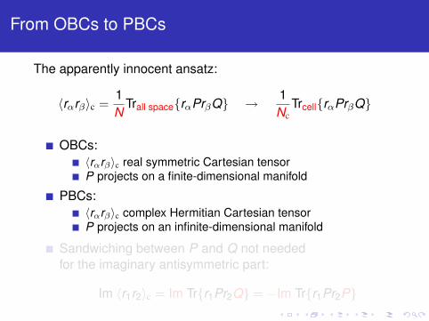
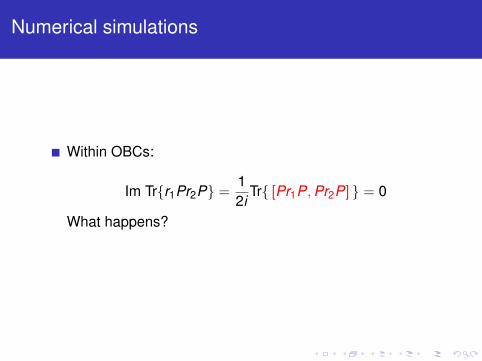
. . . . . .
Numerical simulations
Within OBCs:
Im Trr1Pr2P =12i
Tr [Pr1P,Pr2P] = 0
What happens?
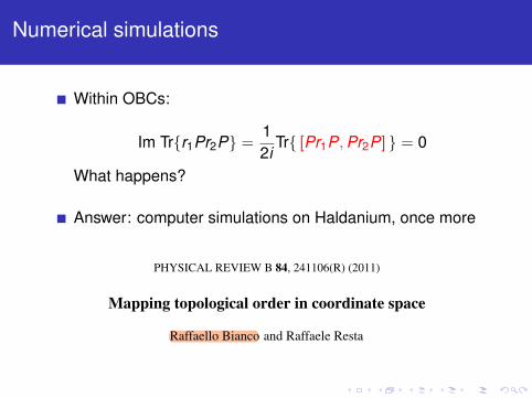
. . . . . .
Numerical simulations
Within OBCs:
Im Trr1Pr2P =12i
Tr [Pr1P,Pr2P] = 0
What happens?
Answer: computer simulations on Haldanium, once moreRAPID COMMUNICATIONS
PHYSICAL REVIEW B 84, 241106(R) (2011)
Mapping topological order in coordinate space
Raffaello Bianco and Raffaele RestaDipartimento di Fisica, Universita di Trieste, Italy, and DEMOCRITOS National Simulation Center, IOM-CNR, Trieste, Italy

. . . . . .
Chern number as a local quantity
Im Trr1Pr2P =12i
Tr [Pr1P,Pr2P]
C1 = −2πiAc
Trcell [Pr1P,Pr2P] ≡ −2πi1Ac
∫celldr ⟨r| [Pr1P,Pr2P] |r⟩
C1 macroscopic average of C(r)
C(r) = −2πi⟨r| [Pr1P,Pr2P] |r⟩ “topological marker”
Can also be interpreted as the curvature per unit area!
Last but not least: Boundary conditions irrelevant
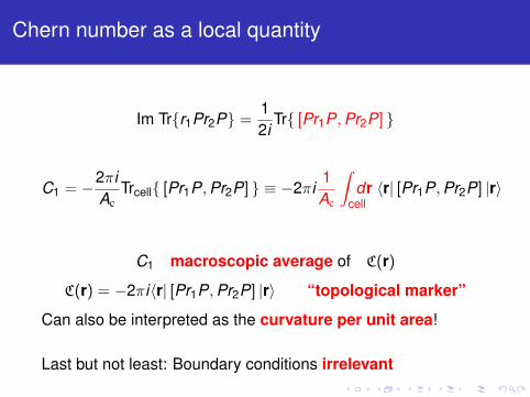
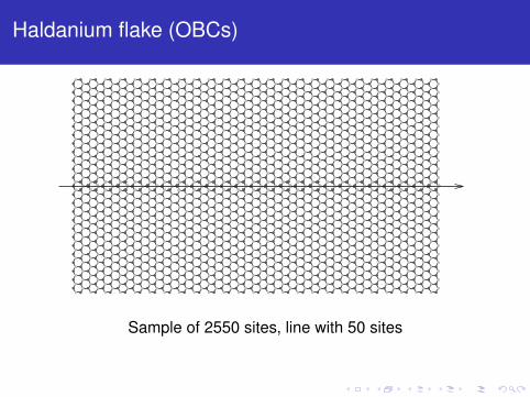
. . . . . .
Haldanium flake (OBCs)
RAPID COMMUNICATIONS
RAFFAELLO BIANCO AND RAFFAELE RESTA PHYSICAL REVIEW B 84, 241106(R) (2011)
Equation (4) becomes then the trace over a crystal cell of areal-space operator:
C = ! 1!
(2! )2
Ac
Im trcellPxQy
= 4!
Ac
Im trcellPxPy, (6)
where the symmetry of the missing term yields the secondline. By exploiting the general properties of projectors and ofthe trace, Eq. (6) can be recast in several equivalent ways.For lattice models, a similar real-space formula has beendemonstrated in 2006 by Kitaev;13 our proof does not relyon lattice models and generalizes Kitaev’s result to realisticimplementations.
Subsequent work adopting Kitaev’s formula was invariablyrooted in k space within a toroidal geometry, for a systemwithout boundaries, and was based on traces.14–17 Finitesystems within open boundary conditions look problematic.In fact, if we replace the trace over the cell with the trace overthe whole sample, the identity
Im trPxPy = 12i
tr[PxP,PyP ] (7)
guarantees a zero result, whenever P projects over a finite-dimensional manifold. This confirms that the global topologyis trivial within open boundary conditions, and also hintsthat traces must be avoided when addressing finite and/orinhomogeneous samples.
At variance with previous work based on Kitaev’s formula,we propose here to directly address the commutator in Eq. (7)before taking the trace. Let X be the projected x coordinate
X(r,r") =!
dr"" P (r,r"")x ""P (r"",r"), (8)
and similarly Y ; we then identify the topological marker withthe local Chern number as10
C(r) = !2! i
!dr"[X(r,r")Y (r",r) ! Y (r,r")X(r",r)]. (9)
Our definition holds within both periodic and open boundaryconditions; given the shortsightedness of P , in a region ofcrystalline periodicity, the cell average of C(r) coincideswith the Chern number C owing to Eq. (6). We expect thedimensionless function C(r) to fluctuate over microscopicdimensions; in the nonperiodic case, the cell average hasto be replaced with the macroscopic average, defined as inelectrostatics (see, e.g., Jackson18).
The gauge invariance of C(r) as defined in Eq. (9) deserves acomment. The ground-state projector P is invariant by unitarytransformations of the occupied orbitals among themselves,but not by a change of the magnetic gauge. However, theunitary operator which transforms P is local in coordinatespace, thus ensuring gauge invariance of C(r).
We validate our formal findings by performing simulationson the Haldane model Hamiltonian;19 it comprises a 2Dhoneycomb lattice with two tight-binding sites per primitivecell with site energies ±", real first-neighbor hoppings t1, andcomplex second-neighbor hoppings t2e
±i# . As a function ofthe parameters, this 2D model system may have either C = 0or C = ±1, according to the phase diagram shown in Fig. 1.
FIG. 1. Chern number of the bottom band of the Haldane modelas a function of the parameters # and "/t2 (t1 = 1,t2 = 1/3). Thepoints marked with letters (a)–(e) in this phase diagram are relevantfor the subsequent discussion and figures. In order to avoid specialfeatures, the # parameter is not a multiple of !/4.
This model has been previously used in several simulations,providing invaluable insight into orbital magnetization5,20,21
as well as into nontrivial topological features of the electronicwave function.5,9,19,22,23 At half filling the system is insulating,except when " = t2 sin # = 0. In this Rapid Communicationwe study, within open boundary conditions, finite flakes ofrectangular shape cut from the bulk, as shown in Fig. 2. Wehave addressed homogenous samples where the Hamiltonianis chosen from various points of the phase diagram (Fig. 1) aswell as disordered and inhomogeneous samples.
Two typical plots for crystalline samples are shown in Fig. 3,where we have chosen the two points (b) and (c) in Fig. 1,with C = 0 and C = 1, respectively. The plots confirm thatthe local Chern numbers C(i) are equal to either 0 or 1 (asexpected) in the bulk of the sample, while they deviate in theboundary region. In both cases the negative values compensatefor the positive ones, given that the sum of the C(i) over thewhole sample vanishes. This compensation is most interestingwhen C = 1 (right-hand panel). A size analysis shows that theminimum negative C(i) value scales as L (linear dimension of
FIG. 2. A typical flake, with 2550 sites, showing the honeycomblattice of the Haldane model (Ref. 19). The 50 sites on the horizontalline will be used in all the subsequent one-dimensional plots.Black and gray circles indicate nonequivalent sites (with on-siteenergies ±").
241106-2
Sample of 2550 sites, line with 50 sites
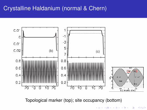
. . . . . .
Crystalline Haldanium (normal & Chern) RAPID COMMUNICATIONS
MAPPING TOPOLOGICAL ORDER IN COORDINATE SPACE PHYSICAL REVIEW B 84, 241106(R) (2011)
FIG. 3. Local Chern number (top) and site occupancy (bottom)for the 50 sites along the line shown in Fig. 2. Left-hand panel: Point(b) in the phase diagram, Fig. 1. Right-hand panel: Point (c). Noticethe different scales.
the sample): The reason is that the number of bulk sites scalesas L2, while the perimeter scales as L.
We have studied both polar (! != 0) and nonpolar (! = 0)cases. While in the latter case the two sites are equivalent, theyare no longer so in the former case. This clearly appears in thesite occupancies, also shown Fig. 3. What is surprising is thatthe corresponding C(i) values do not show any site alternance,while we expect only their cell (or macroscopic) average to beequal to one. We conjecture this to be due to extra symmetrypresent in the Haldane model Hamiltonian, actually broken indisordered samples, discussed below (see Fig. 5).
We have also investigated a few points in the phasediagram close to the transition between C = 0 and C = 1at fixed !/t2 = 3.67 and various " values. Given the finitesize of the system the transition cannot be sharp. The exacttransition for an infinite system occurs at "/# = 0.25; ourresults show that in the bulk of the sample the local Chernnumber is zero up to "/# " 0.17 and one from "/# " 0.29onward. At intermediate values the boundary region broadensconsiderably and indeed invades the whole sample: This isshown in Fig. 4.
FIG. 4. Local Chern number for a few points on the line!/t2 = 3.67, i.e., on the (b)–(c) segment in Fig. 1, close to thetransition from C = 0 to C = 1. The exact transition occurs at"/# = 0.25; our five plots correspond (bottom to top) to "/# =0.17,0.25,0.27,0.29,0.33.
FIG. 5. Local Chern number (top) and site occupancy (bottom)for disordered systems (see text). Left-hand panel: Disordered systemalong the line (a)–(b) in the phase diagram, Fig. 1. Right-hand panel:Line (c)–(d). Notice the different scales.
Typical results for disordered—and macroscopicallyhomogenous—samples are shown in Fig. 5. In the left-handpanel the sign of ! alternates between the two sublattices,while its modulus is chosen at random (with uniform distribu-tion) in the (a)–(b) segment of Fig. 1. In the right-hand panelthe value of ! is chosen at random in the (c)–(d) segment. Itappears clearly that the local Chern numbers C(i) in the bulkof the sample oscillate around a macroscopic average C = 0(left-hand panel) and C = 1 (right-hand panel).
Next we show in Fig. 6 our topological marker across aheterojunction between regions of different topological order,in two typical cases: a normal insulator joined to a C = 1insulator, and a junction where C changes sign. In both casesthe marker maps very perspicuously the actual topologicalorder in the two bulklike regions, while it oscillates at theinterface and at the sample boundary. The virtue of our r-spaceapproach is clearly demonstrated; the conventional k-spaceapproach to topological order cannot separate different regionsof inhomogeneous samples.
Finally we analyze the present results from the viewpointof the modern theory of the insulating state.7,8 Both Eqs. (1)
FIG. 6. Local Chern number (top) and site occupancy (bottom)across heterojunctions. Left-hand panel: Hamiltonian parameters asin (a) and in (b) for the left- and the right-hand halves of the sample,respectively. Right-hand panel: Parameters as in (e) and in (c) for left-and the right-hand halves of the sample.
241106-3
Topological marker (top); site occupancy (bottom)
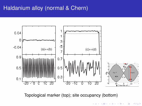
. . . . . .
Haldanium alloy (normal & Chern)RAPID COMMUNICATIONS
MAPPING TOPOLOGICAL ORDER IN COORDINATE SPACE PHYSICAL REVIEW B 84, 241106(R) (2011)
FIG. 3. Local Chern number (top) and site occupancy (bottom)for the 50 sites along the line shown in Fig. 2. Left-hand panel: Point(b) in the phase diagram, Fig. 1. Right-hand panel: Point (c). Noticethe different scales.
the sample): The reason is that the number of bulk sites scalesas L2, while the perimeter scales as L.
We have studied both polar (! != 0) and nonpolar (! = 0)cases. While in the latter case the two sites are equivalent, theyare no longer so in the former case. This clearly appears in thesite occupancies, also shown Fig. 3. What is surprising is thatthe corresponding C(i) values do not show any site alternance,while we expect only their cell (or macroscopic) average to beequal to one. We conjecture this to be due to extra symmetrypresent in the Haldane model Hamiltonian, actually broken indisordered samples, discussed below (see Fig. 5).
We have also investigated a few points in the phasediagram close to the transition between C = 0 and C = 1at fixed !/t2 = 3.67 and various " values. Given the finitesize of the system the transition cannot be sharp. The exacttransition for an infinite system occurs at "/# = 0.25; ourresults show that in the bulk of the sample the local Chernnumber is zero up to "/# " 0.17 and one from "/# " 0.29onward. At intermediate values the boundary region broadensconsiderably and indeed invades the whole sample: This isshown in Fig. 4.
FIG. 4. Local Chern number for a few points on the line!/t2 = 3.67, i.e., on the (b)–(c) segment in Fig. 1, close to thetransition from C = 0 to C = 1. The exact transition occurs at"/# = 0.25; our five plots correspond (bottom to top) to "/# =0.17,0.25,0.27,0.29,0.33.
FIG. 5. Local Chern number (top) and site occupancy (bottom)for disordered systems (see text). Left-hand panel: Disordered systemalong the line (a)–(b) in the phase diagram, Fig. 1. Right-hand panel:Line (c)–(d). Notice the different scales.
Typical results for disordered—and macroscopicallyhomogenous—samples are shown in Fig. 5. In the left-handpanel the sign of ! alternates between the two sublattices,while its modulus is chosen at random (with uniform distribu-tion) in the (a)–(b) segment of Fig. 1. In the right-hand panelthe value of ! is chosen at random in the (c)–(d) segment. Itappears clearly that the local Chern numbers C(i) in the bulkof the sample oscillate around a macroscopic average C = 0(left-hand panel) and C = 1 (right-hand panel).
Next we show in Fig. 6 our topological marker across aheterojunction between regions of different topological order,in two typical cases: a normal insulator joined to a C = 1insulator, and a junction where C changes sign. In both casesthe marker maps very perspicuously the actual topologicalorder in the two bulklike regions, while it oscillates at theinterface and at the sample boundary. The virtue of our r-spaceapproach is clearly demonstrated; the conventional k-spaceapproach to topological order cannot separate different regionsof inhomogeneous samples.
Finally we analyze the present results from the viewpointof the modern theory of the insulating state.7,8 Both Eqs. (1)
FIG. 6. Local Chern number (top) and site occupancy (bottom)across heterojunctions. Left-hand panel: Hamiltonian parameters asin (a) and in (b) for the left- and the right-hand halves of the sample,respectively. Right-hand panel: Parameters as in (e) and in (c) for left-and the right-hand halves of the sample.
241106-3
Topological marker (top); site occupancy (bottom)

. . . . . .
Haldanium heterojunctions
RAPID COMMUNICATIONS
MAPPING TOPOLOGICAL ORDER IN COORDINATE SPACE PHYSICAL REVIEW B 84, 241106(R) (2011)
FIG. 3. Local Chern number (top) and site occupancy (bottom)for the 50 sites along the line shown in Fig. 2. Left-hand panel: Point(b) in the phase diagram, Fig. 1. Right-hand panel: Point (c). Noticethe different scales.
the sample): The reason is that the number of bulk sites scalesas L2, while the perimeter scales as L.
We have studied both polar (! != 0) and nonpolar (! = 0)cases. While in the latter case the two sites are equivalent, theyare no longer so in the former case. This clearly appears in thesite occupancies, also shown Fig. 3. What is surprising is thatthe corresponding C(i) values do not show any site alternance,while we expect only their cell (or macroscopic) average to beequal to one. We conjecture this to be due to extra symmetrypresent in the Haldane model Hamiltonian, actually broken indisordered samples, discussed below (see Fig. 5).
We have also investigated a few points in the phasediagram close to the transition between C = 0 and C = 1at fixed !/t2 = 3.67 and various " values. Given the finitesize of the system the transition cannot be sharp. The exacttransition for an infinite system occurs at "/# = 0.25; ourresults show that in the bulk of the sample the local Chernnumber is zero up to "/# " 0.17 and one from "/# " 0.29onward. At intermediate values the boundary region broadensconsiderably and indeed invades the whole sample: This isshown in Fig. 4.
FIG. 4. Local Chern number for a few points on the line!/t2 = 3.67, i.e., on the (b)–(c) segment in Fig. 1, close to thetransition from C = 0 to C = 1. The exact transition occurs at"/# = 0.25; our five plots correspond (bottom to top) to "/# =0.17,0.25,0.27,0.29,0.33.
FIG. 5. Local Chern number (top) and site occupancy (bottom)for disordered systems (see text). Left-hand panel: Disordered systemalong the line (a)–(b) in the phase diagram, Fig. 1. Right-hand panel:Line (c)–(d). Notice the different scales.
Typical results for disordered—and macroscopicallyhomogenous—samples are shown in Fig. 5. In the left-handpanel the sign of ! alternates between the two sublattices,while its modulus is chosen at random (with uniform distribu-tion) in the (a)–(b) segment of Fig. 1. In the right-hand panelthe value of ! is chosen at random in the (c)–(d) segment. Itappears clearly that the local Chern numbers C(i) in the bulkof the sample oscillate around a macroscopic average C = 0(left-hand panel) and C = 1 (right-hand panel).
Next we show in Fig. 6 our topological marker across aheterojunction between regions of different topological order,in two typical cases: a normal insulator joined to a C = 1insulator, and a junction where C changes sign. In both casesthe marker maps very perspicuously the actual topologicalorder in the two bulklike regions, while it oscillates at theinterface and at the sample boundary. The virtue of our r-spaceapproach is clearly demonstrated; the conventional k-spaceapproach to topological order cannot separate different regionsof inhomogeneous samples.
Finally we analyze the present results from the viewpointof the modern theory of the insulating state.7,8 Both Eqs. (1)
FIG. 6. Local Chern number (top) and site occupancy (bottom)across heterojunctions. Left-hand panel: Hamiltonian parameters asin (a) and in (b) for the left- and the right-hand halves of the sample,respectively. Right-hand panel: Parameters as in (e) and in (c) for left-and the right-hand halves of the sample.
241106-3
Topological marker (top); site occupancy (bottom)
. . . . . .
Outline
1 What topology is about
2 Elements of Berryology
3 Chern insulators
4 Noncrystalline insulators
5 Chern number as a cumulant moment in r space
6 Conclusions
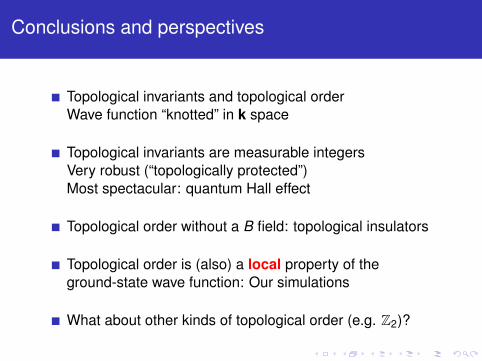
. . . . . .
Conclusions and perspectives
Topological invariants and topological orderWave function “knotted” in k space
Topological invariants are measurable integersVery robust (“topologically protected”)Most spectacular: quantum Hall effect
Topological order without a B field: topological insulators
Topological order is (also) a local property of theground-state wave function: Our simulations
What about other kinds of topological order (e.g. Z2)?

. . . . . .
Collaborators
Davide Ceresoli,now atCNR-ISTM, Milano
Raffaello Bianco,Ph. D. studentat Univ. Trieste