toshiba tecra 500cs and 500cdt - maintenance … tecra 500cs...the toshiba 500 series personal...
TRANSCRIPT

TOSHIBA
500 Series
PN: 500-9400
CAVM-7960284-B00
500 Series 1-1
1.1 Features
The Toshiba 500 Series Personal Computer uses extensive Large Scale Integration (LSI), andComplementary Metal-Oxide Semiconductor (CMOS) technology to provide minimum sizeand weight, low power usage, and high reliability. The computer incorporates the followingfeatures and benefits:
❑ Microprocessor
This computer uses an Intel Pentium processor 120 MHz with VRT (VoltageReduction Technology) that operates at 2.9/3.3 volts. The math co-processor and 16KB cache memory are integrated into Pentium.
❑ Cache memory
256 KB level-2 cache memory is provided in pipe-line burst SRAM.
❑ Hard disk drive
1.3 billion byte (1.26 GB) removable HDD pack.
❑ Selectable Bay
Provides for connection of either an FDD, a CD-ROM, or a second HDD module. AFloppy Disk Drive supports 3.5-inch 2HD (1.44 MB) disks and 2DD (720 KB) disks.The FDD module can be connected to an external FDD port with an attachment whenanother module is installed in the Selectable Bay. A full-size, six-speed CD-ROMdrive contains an ATAPI (AT Attachment Packet Interface) interface controller, andsupports the following formats: audio CD, photo CD, ISO 9660, and CD plus. TheCD-ROM drive is optional on the 500CS. An optional second HDD has 1.3 billionbyte (1.26 GB) capacity.
❑ Memory
Standard with 16 MB of EDO (Extend Data Out) DRAM. This includes 640 KB ofconventional memory and 15488 KB of extended memory.
❑ Display
12.1-inch DSTN (Dual-Scan Supertwist Nematic) color LCD 800 x 600 pixels(500CS). 12.1-inch TFT (Thin Film Transistor) color LCD 800 x 600 pixels(500CDT). The built-in display controller supports full color capability and up to1280 x 1024 resolution on an external monitor.
❑ Keyboard
An-easy-to-use 82/84-key keyboard provides a numeric keypad overlay for fast nu-meric data entry or for cursor and page control. This keyboard supports software thatuses a 101- or 102-key enhanced keyboard.
1-2 500 Series
❑ Batteries
Three different batteries: a Lithium-Ion main battery, a backup battery (for memorybackup), and an RTC battery (Real Time Clock).
❑ Expansion memory slot
An optional 8, 16, 32, 48, or 128 MB memory module can be installed in the memoryslot.
❑ Parallel port
This port can be used to connect a Centronics compatible printer or other paralleldevice. The port supports ECP (Extended Capabilities Port) conforming toIEEE·1284.
❑ Serial port
The serial controller is 16550UART compatible. This standard, 9-pin, serial port canbe used to connect such serial devices as a serial printer, serial mouse, or externalmodem.
❑ External monitor port
The female, 15-pin, D-shell connector can be connected to an external SVGA monitor.This computer supports VESA (Video Electronics Standards Association) DDC(Display Data Channel) 2B compatible functions.
❑ PS/2 mouse/keyboard port
Either a PS/2 compatible keyboard or a PS/2 compatible mouse can be connected tothis port.
❑ PC card slot
A PC card slot can accommodate two Type II (5.0mm) cards or one Type III(10.5mm) card, which support PCMCIA Release 2.01 standard. These slots are readyfor advanced cards, including PC card 16 multifunction cards and CardBus 32-bitcards as well as the ZV (Zoomed Video) port, which is dedicated to high-performancevideo data transfer such as MPEG video playback.
❑ Docking interface port
This 240-pin port enables connection of an Enhanced Port Replicator II or a DeskStation V Plus. The Enhanced Port Replicator II duplicates the following ports on thecomputer: PS/2 keyboard, PS/2 mouse, serial port, parallel port, external CRT, audioline-in, audio line-out, headphone, and microphone. It also provides a joystick portand two additional PC card slots (Type III). The Desk Station V Plus expands addi-tional features to the Enhanced Port Replicator II as follows: two PCI/ISA bus slotsand one PCI bus expansion slot, a 5.25-inch drive bay, a Selectable Bay, and an on-board SCSI-2 (Small Computer System Interface) controller.
500 Series 1-3
❑ External FDD port
The external FDD port lets you connect an external FDD in the attachment when aCD-ROM drive or second HDD is installed in the SelectBay.
❑ AccuPoint
A pointer control stick, located in the center of the keyboard, provides convenientcontrol of the cursor without requiring desk space for a mouse.
❑ Serial infrared port
Incorporates two infrared ports located on the front and back. These ports are com-patible with IrDA1.1 (Infrared Data Association) FIR (Fast Infrared) standard, whichenables cableless 4 Mbps data transfer.
❑ Sound System
Compatible with Sound Blaster Pro and Windows Sound System. This computeris equipped with a microphone, stereo speakers, and the following jacks: audio line-in,audio line-out, headphone, and microphone.
❑ Internal Modem (optional in some markets)
Supports V.34 data communication (28.8Kbps), V.17 class-1 facsimile (14.4Kbps),and voice functions (speaker phone and TAM: Telephone Answering Machine). Thiscomputer is equipped with an RJ11 modem jack to connect a telephone line directly.
1-4 500 Series
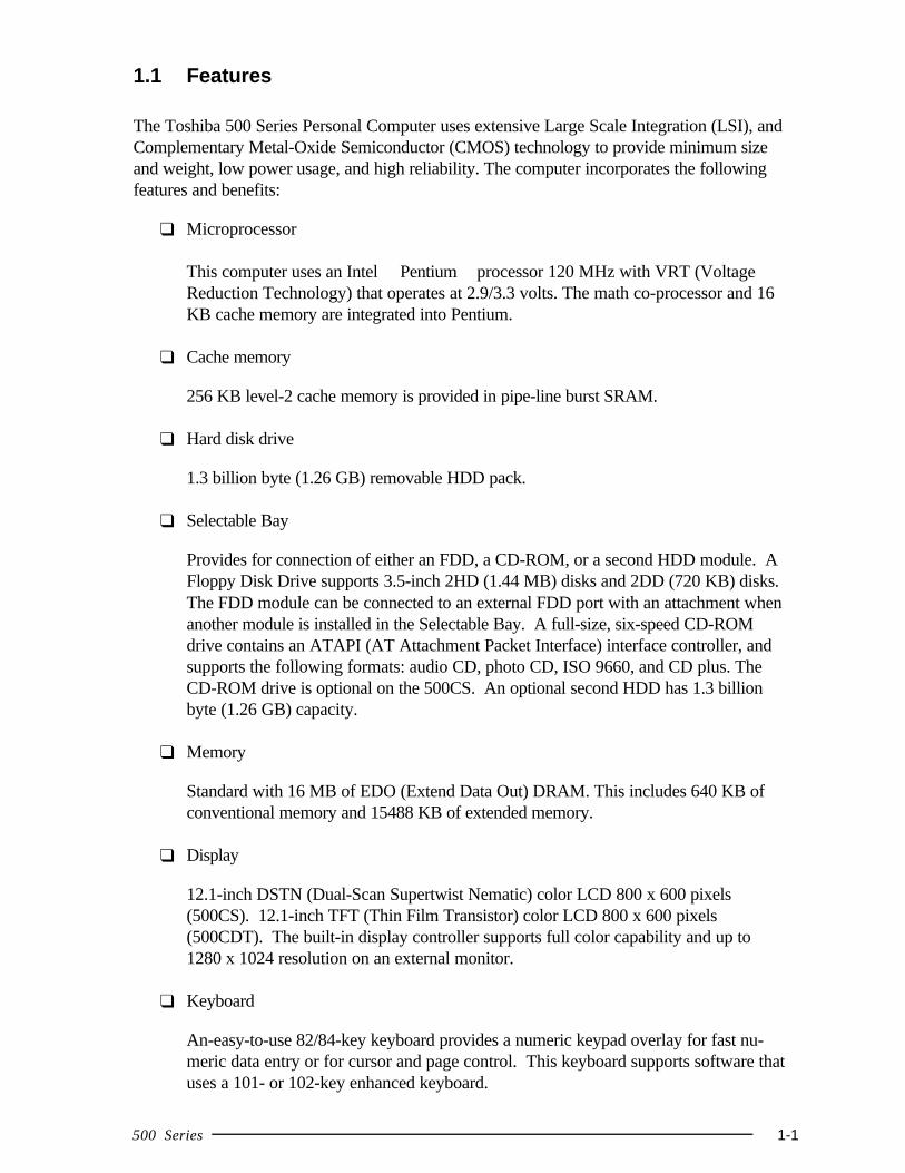
The 500 series Personal Computer is shown in figure 1-1.
Figure 1-1 500 series personal computer
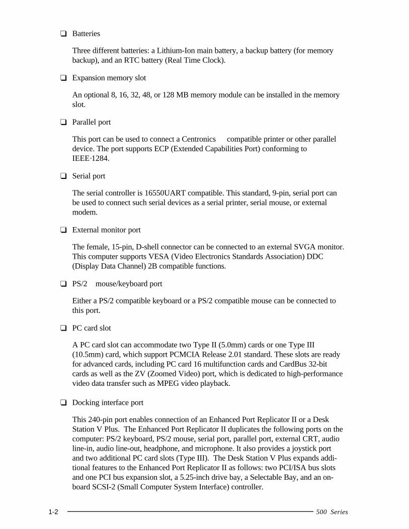
The 500 series system configuration is shown in figure 1-2.
Figure 1-2 500 series system unit configuration
500 Series 1-5
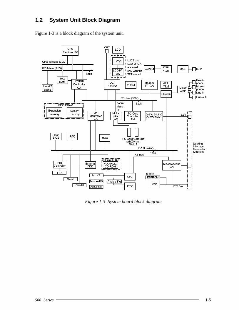
1.2 System Unit Block Diagram
Figure 1-3 is a block diagram of the system unit.
Figure 1-3 System board block diagram
1-6 500 Series
The system board is composed of the following major components:
❑ Intel Pentium processorOperates at 120 MHz and 2.9/3.3 volts. The math co-processor and 16 KBcache memory are integrated into Pentium.
❑ Level-2 cache memoryData RAM: 256 KB
Two 32K x 32-bit pipe-line burst synchronous SRAM chips3.3 volt operationAccess time 8 ns
Tag RAM: 32 KB (only 8 KB is used)One 32K x 8-bit asynchronous SRAM chip3.3 volt operationAccess time 15 ns
The level-2 cache is a direct map method and a write-through policy.
❑ Standard RAM16 MB, eight 1M x 16-bit EDO DRAM chips3.3 volt operationNo parity bitAccess time 60/65 nsData transfer is 64-bit width
❑ BIOS ROM (Flash EEPROM)256 KB, one 256K x 8-bit chip
128 KB used for system BIOS64 KB used for VGA-BIOS8 KB used for plug and play data area8 KB used for password security16 KB used for boot strap32 KB reserved
5 volt operationAccess time 80 nsData transfer is 8-bit width
❑ Optional memoryOne expansion memory slot is available for 8, 16, 32, 48, and 128 MBmemory modules. 8, 16, 32, and 48 MB memory modules consist of some1M x 16-bit chips. 128 MB memory modules consist of some 4M x 16-bitchips.
EDO DRAM is used3.3 volt operationNo parity bitAccess time 60 nsData transfer is 64-bit width
500 Series 1-7
❑ Video RAM2 MB, four 256K x 16-bit EDO DRAM chips5 volt operationAccess time 50 ns
❑ System Controller Gate ArrayThis gate array has the following functions:
CPU interface/controlLevel-2 cache memory controlDRAM controlPCI master/slave interfaceWrite buffer (CPU-DRAM, CPU-PCI, PCI-DRAM)Prefetch buffer (PCI-DRAM)Two DMACs: 82C37 equivalentTwo PICs: 82C59 equivalentOne PIT: 82C54 equivalentSerial interrupt functionPower management controlSuspend/resume controlCPU stop clock function
❑ I/O Controller Gate ArrayThis gate array has the following functions:
Two UARTs 16550A equivalent (One SIO is used for SIR)One FDC µPD765A equivalentOne parallel port control supported ECPISA bus controlPCI bus front end control
❑ Multiplex Gate ArrayThis gate array is a multiplexer for a ZV-port.
❑ LCD Interface Gate Array (TFT only)Controls data transfer between a VGA controller and LVDS
❑ PC Card Controller Gate ArrayThis gate array has the following functions:
PC card controlCardBus controlZV-port support (multiplex gate array control)
1-8 500 Series
❑ Miscellaneous Gate ArrayThis gate array has the following functions:
Communication controlCommunication with KBCI2C bus interface
Communication with PSCommunication with Desk Station V PlusCommunication with EEPROMCommunication register set
PWM controlBeep volume
Speaker controlUniversal I/O portQ-SW control
❑ Modem Interface Gate ArrayControls modem interface LSIs
❑ Video ControllerChips & Technologies F65550 is usedControls internal LCD and external monitor
❑ Keyboard Controller (KBC)One M38802M4 chip is usedIncludes the keyboard scan controller and keyboard interface controller.Controls the internal keyboard, external keyboard, and PS/2 mouse.
❑ AccuPoint Controller (IPSC)One KPAAC0062A chip is usedProvides simultaneous control of both the AccuPoint and a PS/2 mouse.
❑ Real Time Clock (RTC)One T9934 chip is usedThe T9934 has 128 of bytes memory. Fourteen bytes of memory are used forthe calendar and clock. The remaining 114 bytes are used for the systemconfiguration data.
500 Series 1-9
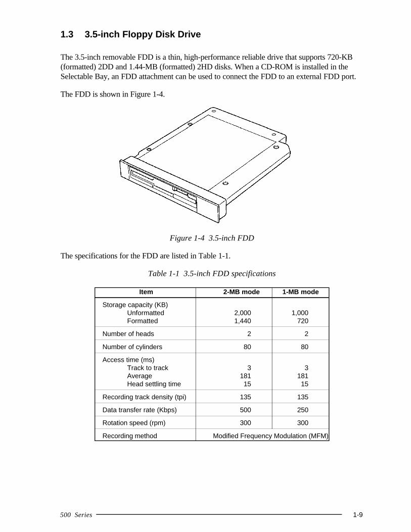
1.3 3.5-inch Floppy Disk Drive
The 3.5-inch removable FDD is a thin, high-performance reliable drive that supports 720-KB(formatted) 2DD and 1.44-MB (formatted) 2HD disks. When a CD-ROM is installed in theSelectable Bay, an FDD attachment can be used to connect the FDD to an external FDD port.
The FDD is shown in Figure 1-4.
Figure 1-4 3.5-inch FDD
The specifications for the FDD are listed in Table 1-1.
Table 1-1 3.5-inch FDD specifications
Item 2-MB mode 1-MB mode
Storage capacity (KB)Unformatted 2,000 1,000Formatted 1,440 720
Number of heads 2 2
Number of cylinders 80 80
Access time (ms)Track to track 3 3Average 181 181Head settling time 15 15
Recording track density (tpi) 135 135
Data transfer rate (Kbps) 500 250
Rotation speed (rpm) 300 300
Recording method Modified Frequency Modulation (MFM)
1-10 500 Series
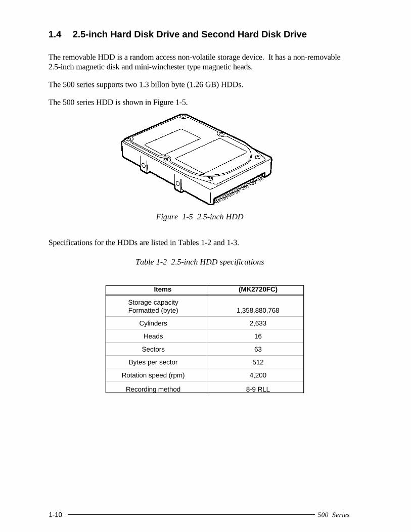
1.4 2.5-inch Hard Disk Drive and Second Hard Disk Drive
The removable HDD is a random access non-volatile storage device. It has a non-removable2.5-inch magnetic disk and mini-winchester type magnetic heads.
The 500 series supports two 1.3 billon byte (1.26 GB) HDDs.
The 500 series HDD is shown in Figure 1-5.
Figure 1-5 2.5-inch HDD
Specifications for the HDDs are listed in Tables 1-2 and 1-3.
Table 1-2 2.5-inch HDD specifications
Items (MK2720FC)
Storage capacityFormatted (byte) 1,358,880,768
Cylinders 2,633
Heads 16
Sectors 63
Bytes per sector 512
Rotation speed (rpm) 4,200
Recording method 8-9 RLL
500 Series 1-11
Table 1-3 Second HDD specifications
Items (MK1301MAV)
Formatted capacity (byte) 1,358,880,768Disks 3
Heads 16
Cylinders 2,633
Sectors 63
Bytes per sector 512
Access time (MS)
Average 13
Track to track 3
Maximum stroke 25
Rotation speed (rpm) 4,200
Data transfer rate (Mbps) 31.8 to 54.8
Buffer size (Kbytes) 128
Power requirement +5V
Power (W)
Seek 3.8
Read/Write 3.2
Idle 1.0
Standby 0.4
Sleep 0.2
1-12 500 Series
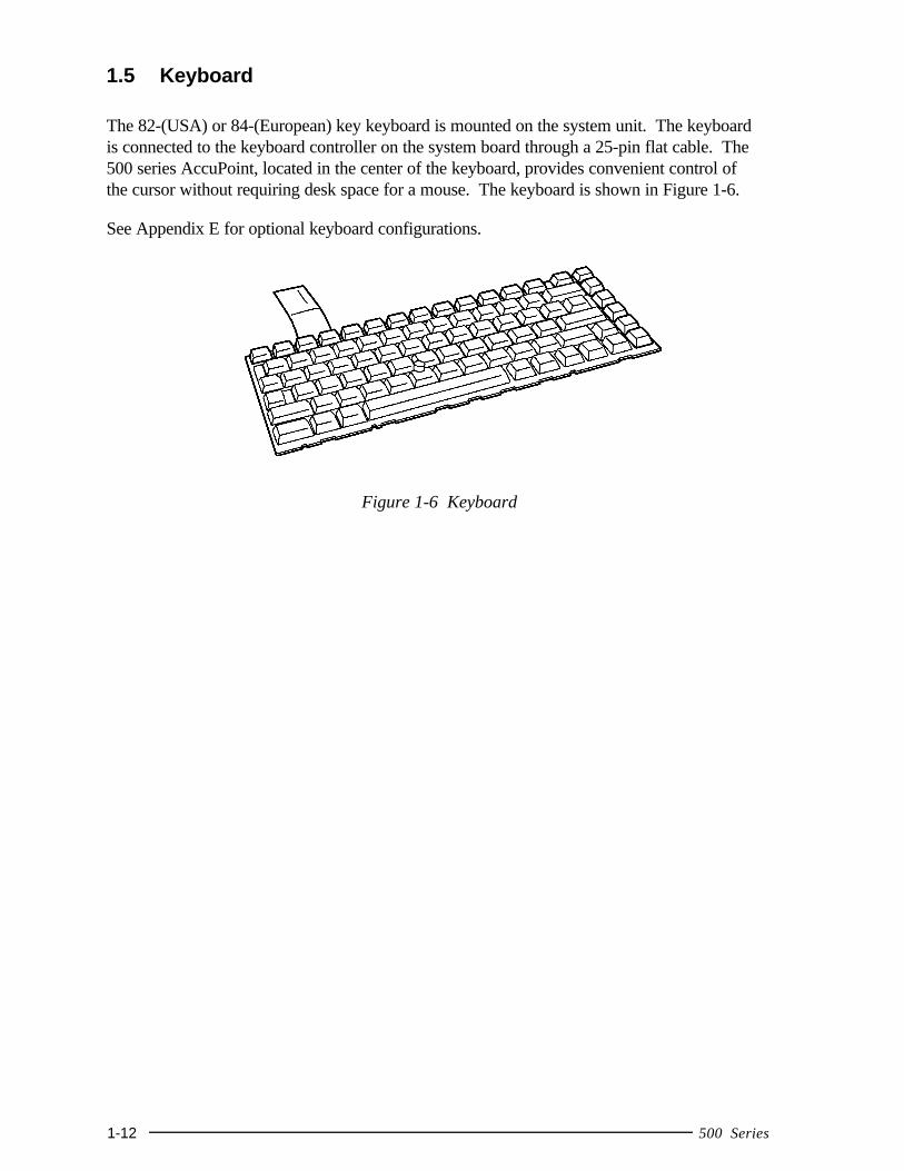
1.5 Keyboard
The 82-(USA) or 84-(European) key keyboard is mounted on the system unit. The keyboardis connected to the keyboard controller on the system board through a 25-pin flat cable. The500 series AccuPoint, located in the center of the keyboard, provides convenient control ofthe cursor without requiring desk space for a mouse. The keyboard is shown in Figure 1-6.
See Appendix E for optional keyboard configurations.
Figure 1-6 Keyboard
500 Series 1-13
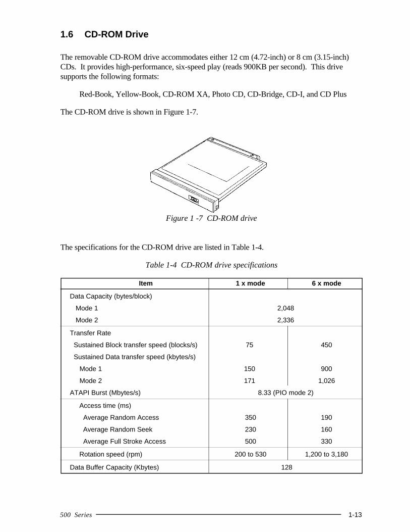
1.6 CD-ROM Drive
The removable CD-ROM drive accommodates either 12 cm (4.72-inch) or 8 cm (3.15-inch)CDs. It provides high-performance, six-speed play (reads 900KB per second). This drivesupports the following formats:
Red-Book, Yellow-Book, CD-ROM XA, Photo CD, CD-Bridge, CD-I, and CD Plus
The CD-ROM drive is shown in Figure 1-7.
Figure 1 -7 CD-ROM drive
The specifications for the CD-ROM drive are listed in Table 1-4.
Table 1-4 CD-ROM drive specifications
Item 1 x mode 6 x mode
Data Capacity (bytes/block)
Mode 1 2,048
Mode 2 2,336
Transfer Rate
Sustained Block transfer speed (blocks/s) 75 450
Sustained Data transfer speed (kbytes/s)
Mode 1 150 900
Mode 2 171 1,026
ATAPI Burst (Mbytes/s) 8.33 (PIO mode 2)
Access time (ms)
Average Random Access 350 190
Average Random Seek 230 160
Average Full Stroke Access 500 330
Rotation speed (rpm) 200 to 530 1,200 to 3,180
Data Buffer Capacity (Kbytes) 128
1-14 500 Series
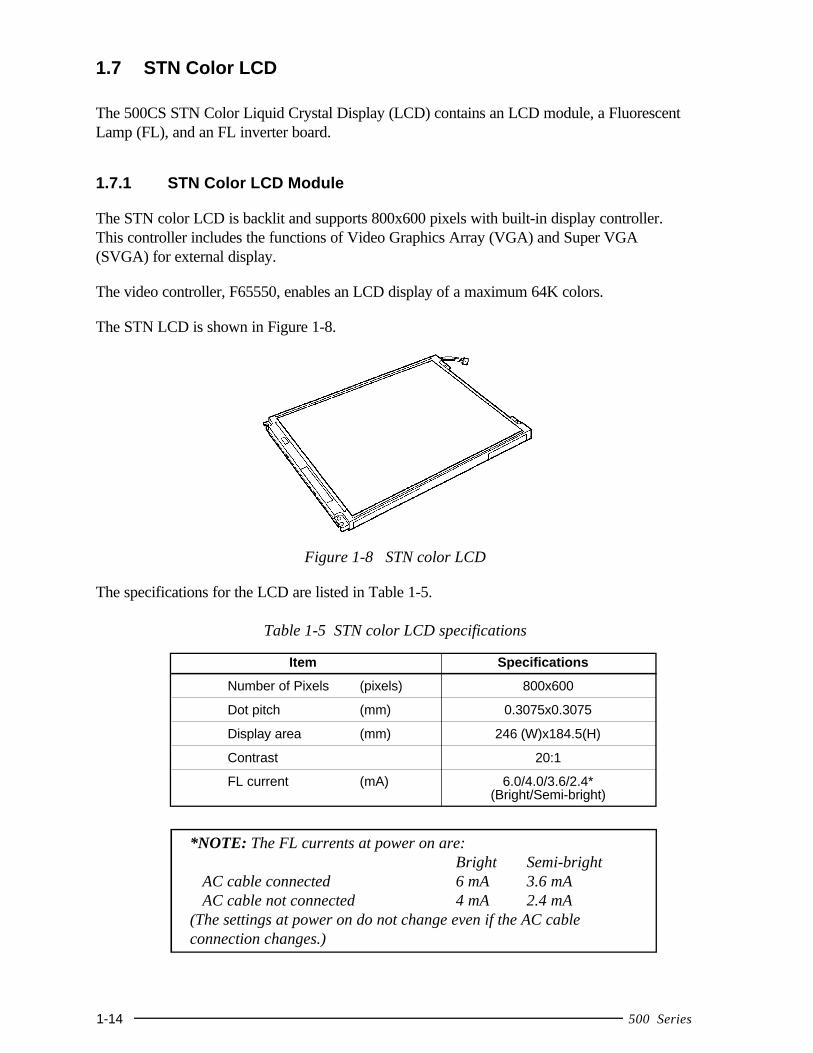
1.7 STN Color LCD
The 500CS STN Color Liquid Crystal Display (LCD) contains an LCD module, a FluorescentLamp (FL), and an FL inverter board.
1.7.1 STN Color LCD Module
The STN color LCD is backlit and supports 800x600 pixels with built-in display controller.This controller includes the functions of Video Graphics Array (VGA) and Super VGA(SVGA) for external display.
The video controller, F65550, enables an LCD display of a maximum 64K colors.
The STN LCD is shown in Figure 1-8.
Figure 1-8 STN color LCD
The specifications for the LCD are listed in Table 1-5.
Table 1-5 STN color LCD specifications
Item Specifications
Number of Pixels (pixels) 800x600
Dot pitch (mm) 0.3075x0.3075
Display area (mm) 246 (W)x184.5(H)
Contrast 20:1
FL current (mA) 6.0/4.0/3.6/2.4*(Bright/Semi-bright)
*NOTE: The FL currents at power on are:Bright Semi-bright
AC cable connected 6 mA 3.6 mA AC cable not connected 4 mA 2.4 mA(The settings at power on do not change even if the AC cableconnection changes.)
500 Series 1-15
1.7.2 Fluorescent Lamp (FL) Inverter Board for STN
The FL inverter board supplies high frequency current to light the LCD’s Fluorescent Lamp.The specifications for the FL inverter are listed in Table 1-6.
Table 1-6 FL inverter board specifications for STN color LCD
Item Specifications
Input Voltage (V) 4 to 5.5
Power (W) 4.8
Output Voltage (Vrms) 1,100
Current (mA) 6.0/4.0/3.6/2.4
1-16 500 Series
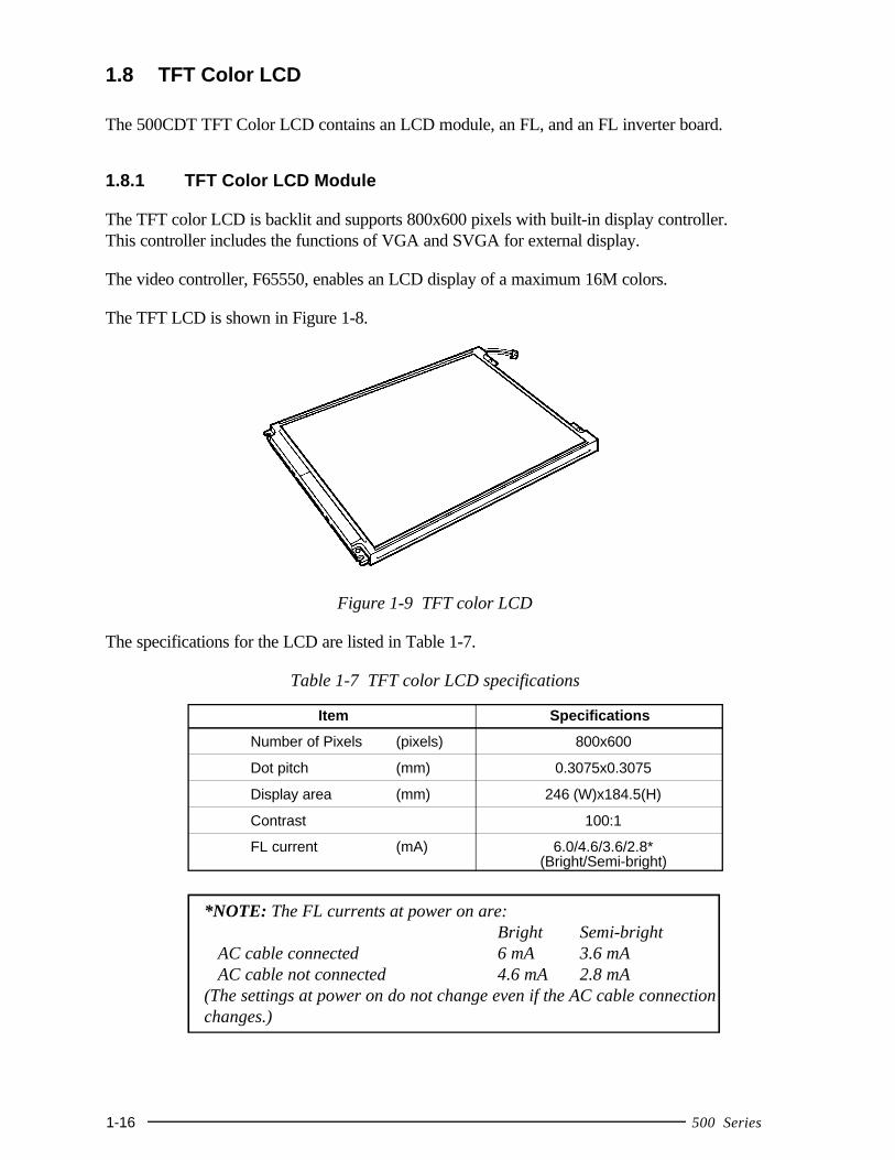
1.8 TFT Color LCD
The 500CDT TFT Color LCD contains an LCD module, an FL, and an FL inverter board.
1.8.1 TFT Color LCD Module
The TFT color LCD is backlit and supports 800x600 pixels with built-in display controller.This controller includes the functions of VGA and SVGA for external display.
The video controller, F65550, enables an LCD display of a maximum 16M colors.
The TFT LCD is shown in Figure 1-8.
Figure 1-9 TFT color LCD
The specifications for the LCD are listed in Table 1-7.
Table 1-7 TFT color LCD specifications
Item Specifications
Number of Pixels (pixels) 800x600
Dot pitch (mm) 0.3075x0.3075
Display area (mm) 246 (W)x184.5(H)
Contrast 100:1
FL current (mA) 6.0/4.6/3.6/2.8*(Bright/Semi-bright)
*NOTE: The FL currents at power on are:Bright Semi-bright
AC cable connected 6 mA 3.6 mA AC cable not connected 4.6 mA 2.8 mA(The settings at power on do not change even if the AC cable connectionchanges.)

500 Series 1-17
1.8.2 Fluorescent Lamp (FL) Inverter Board for TFT
The FL inverter board supplies high frequency current to light the LCD’s Fluorescent Lamp.The specifications for the FL inverter board are listed in Table 1-8.
Table 1-8 FL inverter board specifications for TFT color LCD
Item Specifications
Input Voltage (V) 4 to 5.5
Power (W) 4.8
Output Voltage (Vrms) 1,100
Current (mA) 6.0/4.6/3.6/2.8

1-18 500 Series
1.9 Power Supply
The power supply provides four kinds of voltages to the system board. The power supply hasone microprocessor, operates at 2 MHz, and contains the following functions:
1. Determines if the AC cable or battery is connected to the computer.
2. Detects DC output and circuit malfunctions.
3. Controls the Battery icon and AC IN icon.
4. Turns the battery charging system on and off and detects a fully charged battery.
5. Determines if the power can be turned on and off.
6. Provides more accurate detection of a low battery.
7. Calculates the remaining battery capacity.
8. Detects Ring Indicator (RI) signal for Auto Power On Function.
The power supply output rating is specified in Table 1-9.
Table 1-9 Power supply board output rating
DC Regulation MaximumUse Name voltage tolerance current Ripple
(V) (%) (mA) (mV)
System logic, FDD, HDD B5V +5.0 ±5 3,400 100Display panel, FLand PC card
CPU, RAM, PC card B3V +3.3 ±5 3,800 60
Flash ROM, PC card B12V +12.0 ±5 100 240
System logic MCV +5.0 ±5 5 50
500 Series 1-19
1.10 Batteries
The computer has three types of batteries:
❑ Main battery pack❑ Backup battery❑ RTC battery
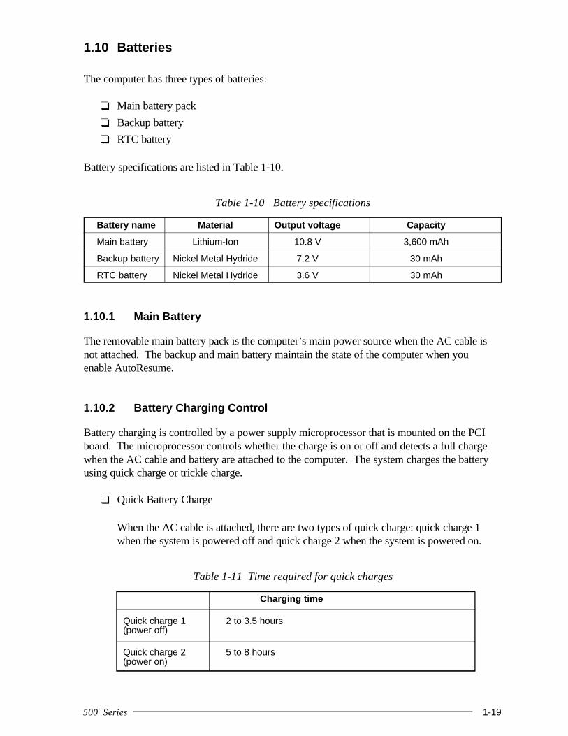
Battery specifications are listed in Table 1-10.
Table 1-10 Battery specifications
Battery name Material Output voltage Capacity
Main battery Lithium-Ion 10.8 V 3,600 mAh
Backup battery Nickel Metal Hydride 7.2 V 30 mAh
RTC battery Nickel Metal Hydride 3.6 V 30 mAh
1.10.1 Main Battery
The removable main battery pack is the computer’s main power source when the AC cable isnot attached. The backup and main battery maintain the state of the computer when youenable AutoResume.
1.10.2 Battery Charging Control
Battery charging is controlled by a power supply microprocessor that is mounted on the PCIboard. The microprocessor controls whether the charge is on or off and detects a full chargewhen the AC cable and battery are attached to the computer. The system charges the batteryusing quick charge or trickle charge.
❑ Quick Battery Charge
When the AC cable is attached, there are two types of quick charge: quick charge 1when the system is powered off and quick charge 2 when the system is powered on.
Table 1-11 Time required for quick charges
Charging time
Quick charge 1 2 to 3.5 hours(power off)
Quick charge 2 5 to 8 hours(power on)
1-20 500 Series
NOTES 1: The time required for quick charge 2 is affected by the amount of powerthe system is consuming. Use of the fluorescent lamp and frequent diskaccess diverts power and lengthens the charge time.
2: Using quick charge 1, the system CPU automatically stops the chargeafter five hours and 30 minutes regardless of the condition of thebattery.
If one of the following occurs, the battery quick charge process stops.
1. The battery becomes fully charged.
2. The AC cable or battery is removed.
3. The battery or output voltage is abnormal.
❑ Trickle Battery Charge
When the main battery is fully charged and the AC cable is attached, the microproces-sor automatically changes quick charge 1 or 2 to trickle charge.
❑ Detection of full charge
A full charge is detected only when the battery is charging at quick charge. A fullcharge is detected under any of the following conditions:
1. The current in the battery charging circuit drops under the predeterminedlimit.
2. The charging time exceeds the fixed limit.
3. The battery’s temperature is over 50°C.
1.10.3 Backup Battery
The backup battery maintains data for AutoResume. The power source used to back-up theAutoResume data is determined according to the following priority:
AC cable > Main battery > Backup battery
The backup battery is charged by the AC cable. Table 1-12 shows the charging time and datapreservation period of the backup battery.
Table 1-12 Backup battery charging/data preservation time
Time
Charging Time 10 H
Data preservation period (full charge) 1.5 H
500 Series 1-21
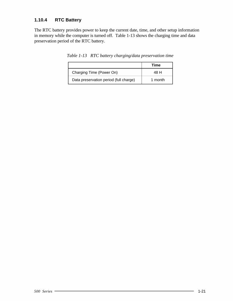
1.10.4 RTC Battery
The RTC battery provides power to keep the current date, time, and other setup informationin memory while the computer is turned off. Table 1-13 shows the charging time and datapreservation period of the RTC battery.
Table 1-13 RTC battery charging/data preservation time
Time
Charging Time (Power On) 48 H
Data preservation period (full charge) 1 month
500 Series 2-1
2.1 Troubleshooting
Chapter 2 describes how to determine if a Field Replaceable Unit (FRU) in the computer iscausing the computer to malfunction. The FRUs covered are:
1. System (FVRSY*) Board 7. Modem (FVRMD*) Board2. PCI (FVRPL*/PS*) Board 8. Floppy Disk Drive3. Sound (FVRSD*) Board 9. Hard Disk Drive4. CardBus (FVRCD*) Board 10. CD-ROM Drive5. LCD FPC (FVRLF*) Board 11. Keyboard
(only for 500CS) 12. Display6. DAA (FLXDA*) Board
NOTE: The DAA (FLXDA*) Board is standard equipment in Canada and the UnitedStates and an option in Europe.
The Diagnostics Disk operations are described in Chapter 3 and Replacement Procedures aredetailed in Chapter 4.
The following tools are necessary for implementing the troubleshooting procedures:
1. Diagnostics Disk2. Phillips screwdriver (2 mm)3. Toshiba MS-DOS system disk(s)
(You must install the following onto the disk: SYS.COM, FORMAT.COM,FDISK.COM and FDISK.EXE)
4. 2DD or 2HD formatted work disk for floppy disk drive testing5. Cleaning kit for floppy disk drive troubleshooting6. Printer port LED7. Printer wraparound connector8. Serial port wraparound connector9. PC Card wraparound card
10. Multimeter11. External monitor12. PS/2 or compatible keyboard13. PS/2 or compatible mouse14. Multimedia sound system with line-in and line-out ports15. Headphone16. Microphone17. Speakers with amplifier18. External FDD attachment19. Lens cleaner for CD-ROM laser pickup lens20. Toshiba-EMI Test Disk TDY-03 for CD-ROM drive.
2-2 500 Series
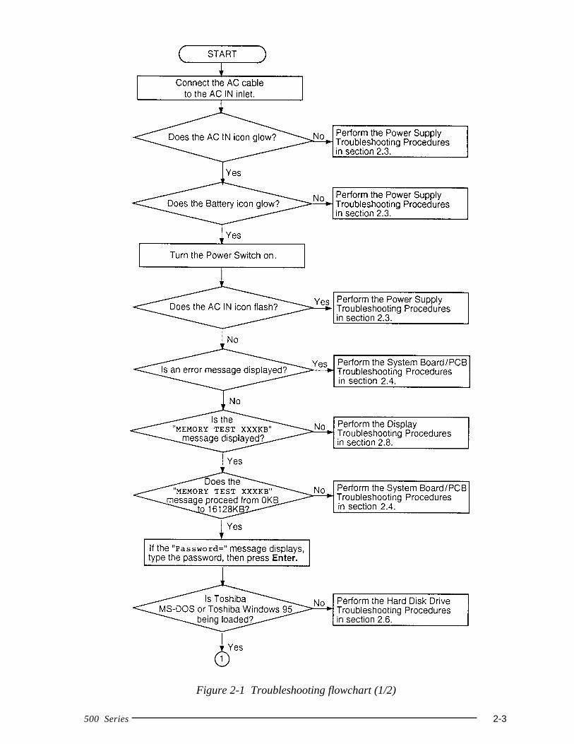
2.2 Troubleshooting Flowchart
Use the flowchart in Figure 2-1 as a guide for determining which troubleshooting proceduresto execute. Before going through the flowchart steps, do the following:
❑ Ask the user if a password is registered and, if it is, ask him or her to enter the pass-word. If the user has forgotten the password, connect the printer port wraparoundboard (F31PRT), then turn the POWER switch on. The computer will override thepassword function by erasing the current password.
❑ Verify with the customer that Toshiba MS-DOS or Toshiba Windows ® 95 is installedon the hard disk. Non-Toshiba operating systems can cause the computer to malfunc-tion.
❑ Make sure all optional equipment is removed from the computer.
❑ Make sure the floppy disk drive is empty.
500 Series 2-3
Figure 2-1 Troubleshooting flowchart (1/2)
2-4 500 Series
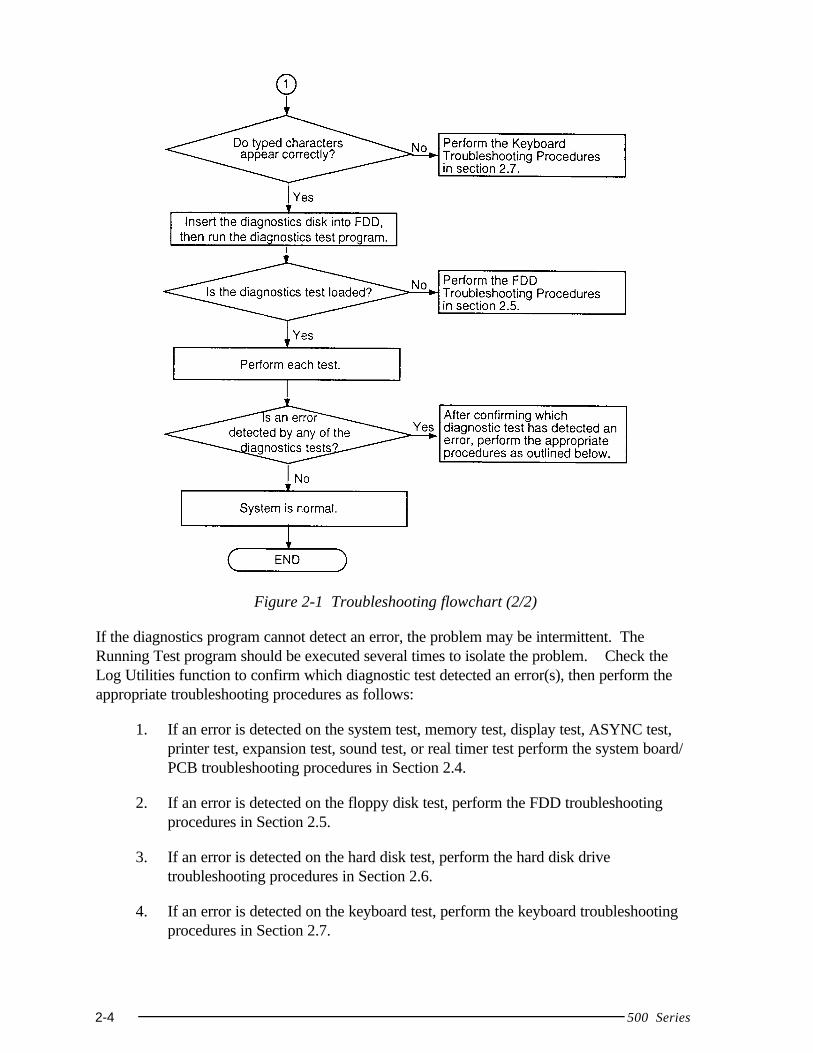
Figure 2-1 Troubleshooting flowchart (2/2)
If the diagnostics program cannot detect an error, the problem may be intermittent. TheRunning Test program should be executed several times to isolate the problem. Check theLog Utilities function to confirm which diagnostic test detected an error(s), then perform theappropriate troubleshooting procedures as follows:
1. If an error is detected on the system test, memory test, display test, ASYNC test,printer test, expansion test, sound test, or real timer test perform the system board/PCB troubleshooting procedures in Section 2.4.
2. If an error is detected on the floppy disk test, perform the FDD troubleshootingprocedures in Section 2.5.
3. If an error is detected on the hard disk test, perform the hard disk drivetroubleshooting procedures in Section 2.6.
4. If an error is detected on the keyboard test, perform the keyboard troubleshootingprocedures in Section 2.7.
500 Series 2-5
5. If an error is detected on the display test, perform the display troubleshootingprocedures in Section 2.8.
6. If an error is detected on the CD-ROM test, perform the CD-ROM drive trouble-shooting procedures in Section 2.9.
7. If an error is detected on the modem test, perform the modem troubleshootingprocedures in Section 2.10.
2-6 500 Series
2.3 Power Supply Troubleshooting
The power supply controls many functions and components. To determine if the power supplyis functioning properly, start with Procedure 1 and continue with the other Procedures asinstructed. The procedures described in this section are:
Procedure 1: Power Status Check
Procedure 2: Error Code Check
Procedure 3: Connection Check
Procedure 4: Quick Charge Check
Procedure 5: Replacement Check
500 Series 2-7
Procedure 1 Power Status Check
The following icons indicate the power supply status:
❑ Battery icon❑ AC IN icon
The power supply controller displays the power supply status through the Battery and the ACIN icons as shown in the tables below.
Table 2-1 Battery icon
Battery icon Power supply status
Lights yellow Quick charge
Lights green Battery has a full charge and the AC cable is connected
Blinks yellow The battery level becomes low while operating the computer on
(even intervals) battery power*1
Flashes yellow The power switch is pressed on when the battery level is low*2
Doesn’t light Any condition other than those above
*1 AutoResume Off will be executed soon.*2 AutoResume Off has already been executed.
Table 2-2 AC IN icon
AC IN icon Power supply status
Lights green DC power is being supplied from the AC PS unit, Desk Station V Plus
Blinks green Power supply malfunction*3
Doesn’t light Any condition other than those above
*3 When the power supply controller detects a malfunction, the AC IN iconblinks and an error code is displayed.
To check the power supply status, install a battery pack and connect an AC PS unit.
Check 1 If the AC IN icon flashes yellow, go to Procedure 2.
Check 2 If the AC IN icon does not light, go to Procedure 3.
Check 3 If the Battery icon does not light yellow or green, go to Procedure 4.
2-8 500 Series
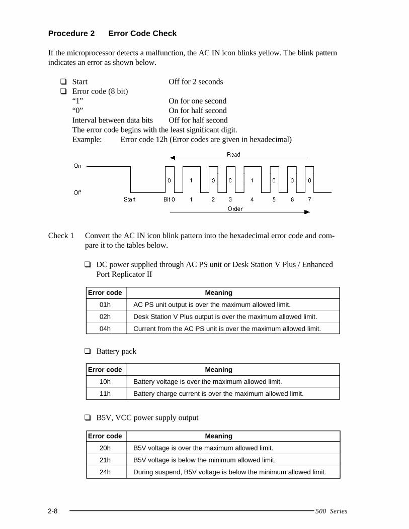
Procedure 2 Error Code Check
If the microprocessor detects a malfunction, the AC IN icon blinks yellow. The blink patternindicates an error as shown below.
❑ Start Off for 2 seconds❑ Error code (8 bit)
“1” On for one second“0” On for half secondInterval between data bits Off for half secondThe error code begins with the least significant digit.Example: Error code 12h (Error codes are given in hexadecimal)
Check 1 Convert the AC IN icon blink pattern into the hexadecimal error code and com-pare it to the tables below.
❑ DC power supplied through AC PS unit or Desk Station V Plus / EnhancedPort Replicator II
Error code Meaning
01h AC PS unit output is over the maximum allowed limit.
02h Desk Station V Plus output is over the maximum allowed limit.
04h Current from the AC PS unit is over the maximum allowed limit.
❑ Battery pack
Error code Meaning
10h Battery voltage is over the maximum allowed limit.
11h Battery charge current is over the maximum allowed limit.
❑ B5V, VCC power supply output
Error code Meaning
20h B5V voltage is over the maximum allowed limit.
21h B5V voltage is below the minimum allowed limit.
24h During suspend, B5V voltage is below the minimum allowed limit.
500 Series 2-9
❑ B3V output
Error code Meaning
30h B3V Voltage is over the maximum allowed limit.
31h B3V Voltage is below the minimum allowed limit.
33h B3V is below the minimum allowed limit during suspend.
❑ B12V Output
Error code Meaning
40h B12V Voltage is over the maximum allowed limit.
41h B12V Voltage is below the minimum allowed limit.
❑ Environmental condition
Error code Meaning
80h CPU temperature is outside the allowable range.
88h The CPU overheats, the system enters resume mode and automati-cally shuts down.
Check 2 In case of error code 01h:
❑ Make sure the AC power cord is firmly plugged into the AC inlet and walloutlet. If this cable is connected correctly, go to the following step:
❑ Make sure the DC power cord of the AC PS unit is firmly plugged into theconnector. If this cable is connected correctly, go to the following step:
❑ Replace the AC PS unit with a new one. If the error still exists, go toProcedure 5.
Check 3 In case of error code 02h:
❑ Make sure the Desk Station V Plus is firmly connected to the computer’sdocking interface port. If this port is connected correctly, go to followingstep:
❑ Check the connector visually to make sure no pins are bent. If a pin(s) is bent,go to Chapter 4, Replacement Procedures. If the connector is not physicallydamaged, go to the following step:
❑ Check the Desk Station V Plus for malfunctions. Refer to the Desk Station VPlus maintenance manual for details. If the error still exists, go to Procedure 5.
2-10 500 Series
Check 4 In case of error code 10h:
❑ Make sure the battery pack is correctly installed in the computer. If the batterypack is correctly installed, go to the following step:
❑ Replace the battery pack with a new one. If the error still exists, go toProcedure 5.
Check 5 When 80h is displayed, it indicates that the CPU temperature is outside the allow-able operating range. Perform the following steps:
❑ Leave the computer in an area that is about room temperature until the CPU’sinternal temperature is within the allowable operating range.
❑ If the error still exists, go to Procedure 5.
Check 6 When 88h is displayed, it indicates that the CPU temperature is too high. Thecomputer automatically enters resume mode and shuts down.
❑ Leave the computer off until the AC IN icon stops blinking. It is recom-mended to leave the computer off until its interior reaches room temperatureeven though the AC IN icon stops blinking.
❑ If the error still exists, go to Procedure 5.
Check 7 For any other error, go to Procedure 5.
Procedure 3 Connection Check
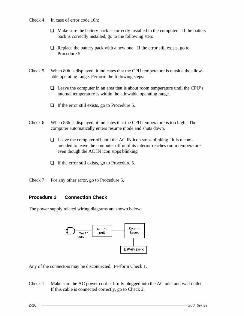
The power supply related wiring diagrams are shown below:
Any of the connectors may be disconnected. Perform Check 1.
Check 1 Make sure the AC power cord is firmly plugged into the AC inlet and wall outlet.If this cable is connected correctly, go to Check 2.
500 Series 2-11
Check 2 • If the AC IN icon does not glow green, go to Procedure 5.• If the Battery icon does not glow orange, go to Check 3.
Check 3 Make sure the battery pack is installed in the computer correctly. If the battery isproperly installed and the Battery icon still does not glow orange, go to Procedure4.
Procedure 4 Quick Charge Check
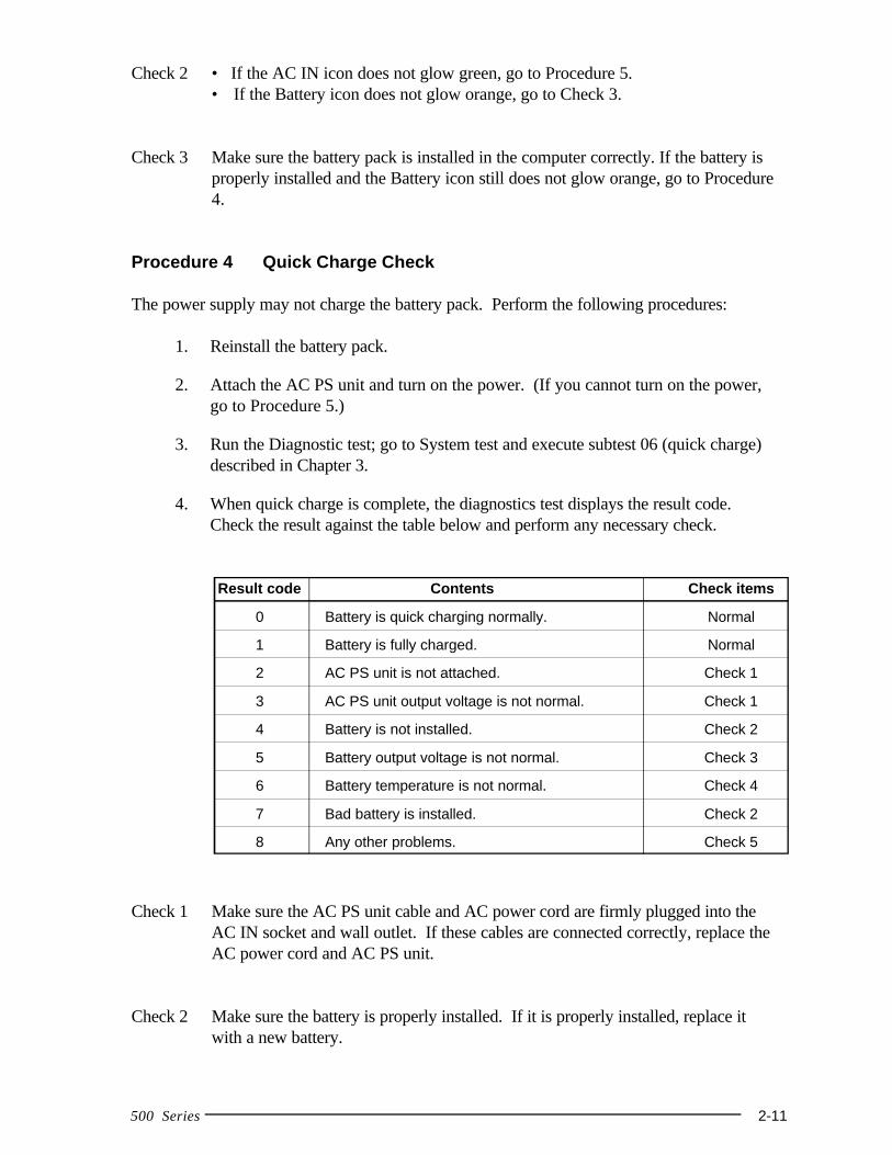
The power supply may not charge the battery pack. Perform the following procedures:
1. Reinstall the battery pack.
2. Attach the AC PS unit and turn on the power. (If you cannot turn on the power,go to Procedure 5.)
3. Run the Diagnostic test; go to System test and execute subtest 06 (quick charge)described in Chapter 3.
4. When quick charge is complete, the diagnostics test displays the result code.Check the result against the table below and perform any necessary check.
Result code Contents Check items
0 Battery is quick charging normally. Normal
1 Battery is fully charged. Normal
2 AC PS unit is not attached. Check 1
3 AC PS unit output voltage is not normal. Check 1
4 Battery is not installed. Check 2
5 Battery output voltage is not normal. Check 3
6 Battery temperature is not normal. Check 4
7 Bad battery is installed. Check 2
8 Any other problems. Check 5
Check 1 Make sure the AC PS unit cable and AC power cord are firmly plugged into theAC IN socket and wall outlet. If these cables are connected correctly, replace theAC power cord and AC PS unit.
Check 2 Make sure the battery is properly installed. If it is properly installed, replace itwith a new battery.
2-12 500 Series
Check 3 The battery pack will be completely discharged. Wait a few minutes to charge thebattery pack. If the battery pack still isn’t charged, replace the battery pack with anew one.
Check 4 The battery temperature is hot or cold. Return the temperature to normal operat-ing condition.
If the battery pack still doesn’t charge, replace the battery pack with a new one.
Check 5 Go to Procedure 5.
Procedure 5 Replacement Check
The system board may be disconnected or damaged. Disassemble the computer following thesteps described in Chapter 4, Replacement Procedures, and check the connection betweenpower supply board and system board. After checking the connection, perform the followingcheck:
Check 1 Replace the system board with a new one.
500 Series 2-13
2.4 System Board/PCB Troubleshooting
This section describes how to determine if the system board or other PCBs are defective ornot functioning properly. Start with Procedure 1 and continue with the other procedures asinstructed. The procedures described in this section are:
Procedure 1: Message Check
Procedure 2: Printer Port LED Check on Boot Mode
Procedure 3: Printer Port LED Check on Resume Mode
Procedure 4: Diagnostic Test Program Execution Check
Procedure 5: Replacement Check
Procedure 1 Message Check
When the power is turned on, the system performs the Initial Reliability Test (IRT) installed inthe BIOS ROM. The IRT tests each IC on the system board and initializes it.
❑ If an error message is shown on the display, perform Check 1.
❑ If there is no error message, go to Procedure 2.
❑ If Toshiba MS-DOS or Toshiba Windows 95 is properly loaded, go toProcedure 3.
Check 1 If one of the following error messages is displayed on the screen, press the F1 keyas the message instructs. These errors occur when the system configurationpreserved in the RTC memory (CMOS type memory) is not the same as the actualconfiguration or when the data is lost.
If you press the F1 key as the message instructs, the TSETUP screen appears toset the system configuration. If error message (b) appears often when the power isturned on, replace the RTC battery. If any other error message is displayed,perform Check 2.
(a) *** Bad HDD type ***Check system. Then press [F1] key ......
(b) *** Bad RTC battery ***Check system. Then press [F1] key ......
(c) *** Bad configuration ***Check system. Then press [F1] key ......
(d) *** Bad memory size ***Check system. Then press [F1] key ......
(e) *** Bad time function ***Check system. Then press [F1] key ......
(f) *** Bad check sum (CMOS) ***Check system. Then press [F1] key ......
(g) *** Bad check sum (ROM) ***Check system. Then press [F1] key ......
2-14 500 Series
Check 2 If the following error message displays, press any key as the message instructs.
WARNING: RESUME FAILURE.PRESS ANY KEY TO CONTINUE.
This message appears when data stored in RAM under the resume function is lostbecause the battery has become discharged or the system board is damaged. Goto Procedure 3.
If any other message appears, perform Check 3.
Check 3 The IRT checks the system board. When the IRT detects an error, the systemstops or an error message appears.
If one of the following error messages (1) through (17), (24) or (25) is displayed,replace the system board.
If error message (18) is displayed, go to the Keyboard Troubleshooting Proce-dures in section 2.7.
If error message (19), (20) or (21) is displayed, go to the HDD TroubleshootingProcedures in section 2.6.
If error message (22) or (23) is displayed, go to the FDD Troubleshooting Proce-dures in section 2.5.
(1) PIT ERROR(2) MEMORY REFRESH ERROR(3) TIMER CH.2 OUT ERROR(4) CMOS CHECKSUM ERROR(5) CMOS BAD BATTERY ERROR(6) FIRST 64KB MEMORY ERROR(7) FIRST 64KB MEMORY PARITY ERROR(8) VRAM ERROR(9) SYSTEM MEMORY ERROR(10) SYSTEM MEMORY PARITY ERROR(11) EXTENDED MEMORY ERROR(12) EXTENDED MEMORY PARITY ERROR(13) DMA PAGE REGISTER ERROR(14) DMAC #1 ERROR(15) DMAC #2 ERROR(16) PIC #1 ERROR(17) PIC #2 ERROR(18) KBC ERROR(19) HDC ERROR(20) HDD #0 ERROR(21) HDD #1 ERROR(22) NO FDD ERROR(23) FDC ERROR(24) TIMER INTERRUPT ERROR(25) RTC UPDATE ERROR
500 Series 2-15
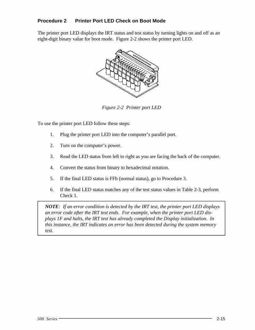
Procedure 2 Printer Port LED Check on Boot Mode
The printer port LED displays the IRT status and test status by turning lights on and off as aneight-digit binary value for boot mode. Figure 2-2 shows the printer port LED.
Figure 2-2 Printer port LED
To use the printer port LED follow these steps:
1. Plug the printer port LED into the computer’s parallel port.
2. Turn on the computer’s power.
3. Read the LED status from left to right as you are facing the back of the computer.
4. Convert the status from binary to hexadecimal notation.
5. If the final LED status is FFh (normal status), go to Procedure 3.
6. If the final LED status matches any of the test status values in Table 2-3, performCheck 1.
NOTE: If an error condition is detected by the IRT test, the printer port LED displaysan error code after the IRT test ends. For example, when the printer port LED dis-plays 1F and halts, the IRT test has already completed the Display initialization. Inthis instance, the IRT indicates an error has been detected during the system memorytest.
2-16 500 Series
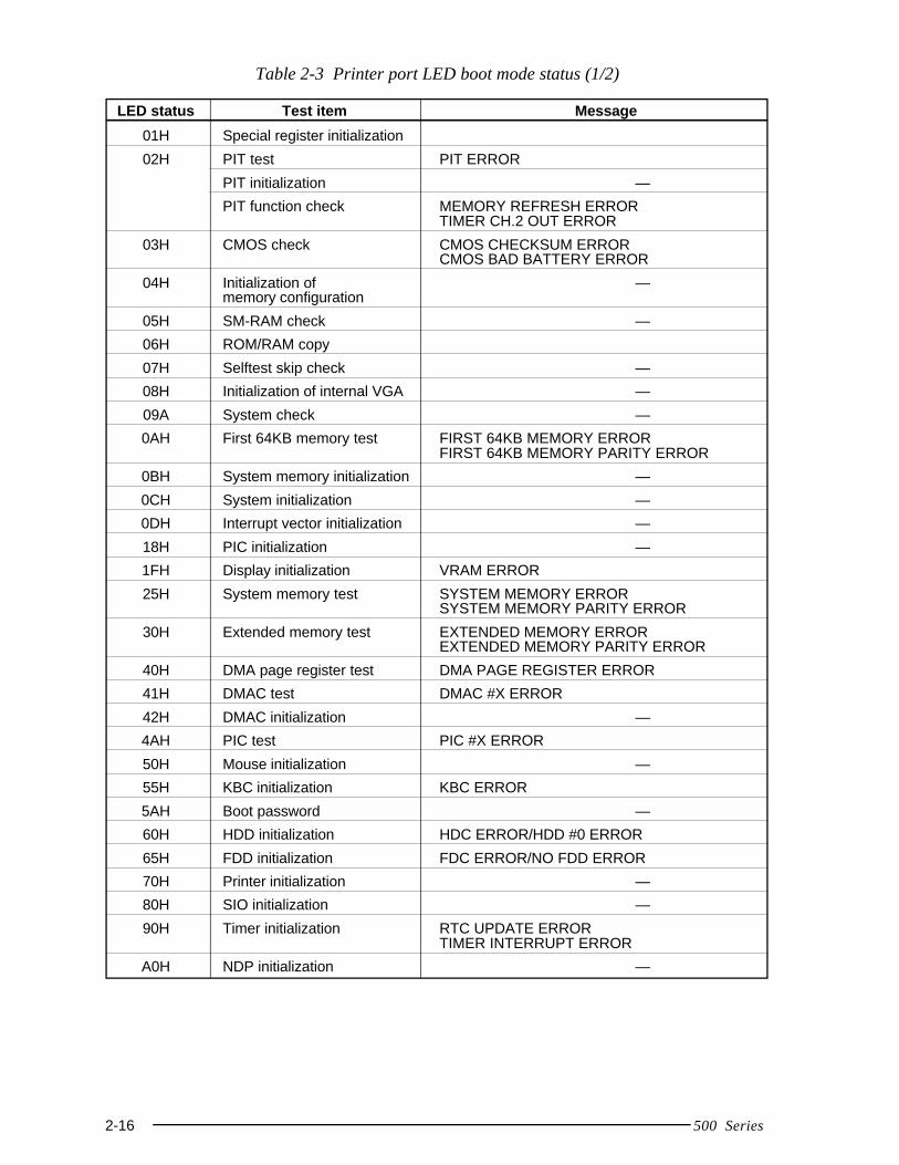
Table 2-3 Printer port LED boot mode status (1/2)
LED status Test item Message
01H Special register initialization
02H PIT test PIT ERROR
PIT initialization —
PIT function check MEMORY REFRESH ERRORTIMER CH.2 OUT ERROR
03H CMOS check CMOS CHECKSUM ERRORCMOS BAD BATTERY ERROR
04H Initialization of —memory configuration
05H SM-RAM check —
06H ROM/RAM copy
07H Selftest skip check —
08H Initialization of internal VGA —
09A System check —
0AH First 64KB memory test FIRST 64KB MEMORY ERRORFIRST 64KB MEMORY PARITY ERROR
0BH System memory initialization —
0CH System initialization —
0DH Interrupt vector initialization —
18H PIC initialization —
1FH Display initialization VRAM ERROR
25H System memory test SYSTEM MEMORY ERRORSYSTEM MEMORY PARITY ERROR
30H Extended memory test EXTENDED MEMORY ERROREXTENDED MEMORY PARITY ERROR
40H DMA page register test DMA PAGE REGISTER ERROR
41H DMAC test DMAC #X ERROR
42H DMAC initialization —
4AH PIC test PIC #X ERROR
50H Mouse initialization —
55H KBC initialization KBC ERROR
5AH Boot password —
60H HDD initialization HDC ERROR/HDD #0 ERROR
65H FDD initialization FDC ERROR/NO FDD ERROR
70H Printer initialization —
80H SIO initialization —
90H Timer initialization RTC UPDATE ERRORTIMER INTERRUPT ERROR
A0H NDP initialization —
500 Series 2-17
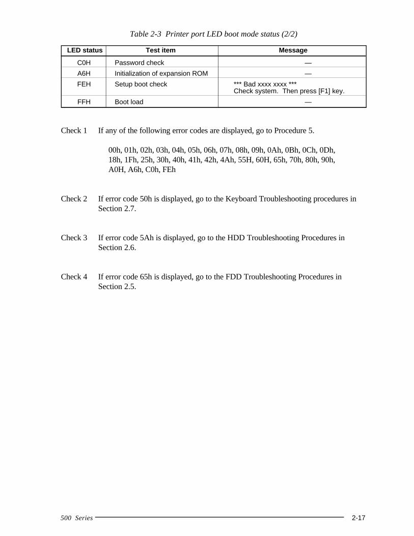
Table 2-3 Printer port LED boot mode status (2/2)
LED status Test item Message
C0H Password check —
A6H Initialization of expansion ROM —
FEH Setup boot check *** Bad xxxx xxxx ***Check system. Then press [F1] key.
FFH Boot load —
Check 1 If any of the following error codes are displayed, go to Procedure 5.
00h, 01h, 02h, 03h, 04h, 05h, 06h, 07h, 08h, 09h, 0Ah, 0Bh, 0Ch, 0Dh,18h, 1Fh, 25h, 30h, 40h, 41h, 42h, 4Ah, 55H, 60H, 65h, 70h, 80h, 90h,A0H, A6h, C0h, FEh
Check 2 If error code 50h is displayed, go to the Keyboard Troubleshooting procedures inSection 2.7.
Check 3 If error code 5Ah is displayed, go to the HDD Troubleshooting Procedures inSection 2.6.
Check 4 If error code 65h is displayed, go to the FDD Troubleshooting Procedures inSection 2.5.
2-18 500 Series
Procedure 3 Printer Port LED Check on Resume Mode
The printer port LED displays the IRT status and test status by turning lights on and off as aneight-digit binary value for resume mode.
To use the printer port LED follow these steps:
1. Make sure the computer is in resume mode.
2. Plug the printer port LED into the computer’s parallel port.
3. Turn on the computer’s power.
4. Read the LED status from left to right as you face the back of the computer.
5. Convert the status from binary to hexadecimal notation.
6. If the final LED status is FFh (normal status), go to Procedure 4.
7. If the final LED status matches any of the test status values in Table 2-4, performProcedure 5.
Table 2-4 Printer port LED resume mode error status
Error status Meaning of status
F1H System BIOS RAM checksum error
F2H External display card is connected
F3H HDD was installed
F4H SMRAM checksum error or memory error during suspend
F5H Conventional memory checksum error
F6H Video RAM checksum error
F7H Extended memory checksum error
F8H PnP RAM checksum error
500 Series 2-19
Procedure 4 Diagnostic Test Program Execution Check
Execute the following tests from the Diagnostic Test Menu. Refer to Chapter 3, Tests andDiagnostics, for more information on how to perform these tests.
1. System test2. Memory test3. Printer test4. ASYNC test5. Real Timer test6. Expansion test7. Sound test8. Modem test
If an error is detected during any of these tests, go to Procedure 5.
2-20 500 Series
Procedure 5 Replacement Check
The system board or other PCBs may be damaged. Disassemble the computer following thesteps described in Chapter 4, Replacement Procedures, and perform the following checks:
❑ If the System test, Memory test, Printer test, Expansion test, Async test, orReal Timer test detects an error, go to Check 1.
❑ If the Sound test detects an error, go to Check 2.
❑ If the Modem test detects an error, go to Check 4.
NOTE: Refer to Chapter 4 for instructions on how to remove and replace any of thefollowing boards.
Check 1 Replace the system board with a new one. If the problem still exists, go to Check6.
Check 2 Replace the sound board with a new one. If the problem still exists, go to Check3.
Check 3 Replace the flat cable with a new one. If the problem still exists, go to Check 6.
Check 4 Replace the DAA board with a new one. If the problem still exists, go to Check 5.
Check 5 Replace the modem board with a new one. If the problem still exists, go to Check6.
Check 6 Replace the PCI (Upper System) board with a new one.
500 Series 2-21
2.5 Floppy Disk Drive Troubleshooting
This section describes how to determine if the FDD is functioning properly. Perform the stepsbelow starting with Procedure 1 and continuing with the other procedures as required.
Procedure 1: FDD Head Cleaning Check
Procedure 2: Diagnostic Test Program Execution Check
Procedure 3: Connector Check and Replacement Check
Procedure 1 FDD Head Cleaning Check
FDD head cleaning is one option available in the Diagnostic Program. A detailed operation isgiven in Chapter 3, Tests and Diagnostics.
Insert the Diagnostics disk into the computer’s floppy disk drive, turn on the computer, andrun the test. Clean the FDD heads using the cleaning kit. If the FDD still does not functionproperly after cleaning, go to Procedure 3.
If the test program cannot be executed on the computer, go to Procedure 3.
2-22 500 Series
Procedure 2 Diagnostic Test Program Execution Check
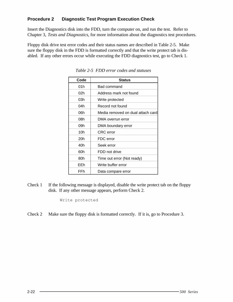
Insert the Diagnostics disk into the FDD, turn the computer on, and run the test. Refer toChapter 3, Tests and Diagnostics, for more information about the diagnostics test procedures.
Floppy disk drive test error codes and their status names are described in Table 2-5. Makesure the floppy disk in the FDD is formatted correctly and that the write protect tab is dis-abled. If any other errors occur while executing the FDD diagnostics test, go to Check 1.
Table 2-5 FDD error codes and statuses
Code Status
01h Bad command
02h Address mark not found
03h Write protected
04h Record not found
06h Media removed on dual attach card
08h DMA overrun error
09h DMA boundary error
10h CRC error
20h FDC error
40h Seek error
60h FDD not drive
80h Time out error (Not ready)
EEh Write buffer error
FFh Data compare error
Check 1 If the following message is displayed, disable the write protect tab on the floppydisk. If any other message appears, perform Check 2.
Write protected
Check 2 Make sure the floppy disk is formatted correctly. If it is, go to Procedure 3.
500 Series 2-23
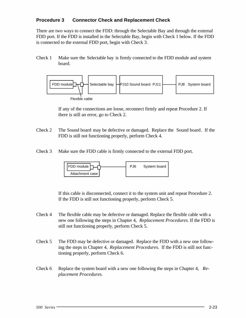
Procedure 3 Connector Check and Replacement Check
There are two ways to connect the FDD: through the Selectable Bay and through the externalFDD port. If the FDD is installed in the Selectable Bay, begin with Check 1 below. If the FDDis connected to the external FDD port, begin with Check 3.
Check 1 Make sure the Selectable bay is firmly connected to the FDD module and systemboard.
FDD module Selectable bay PJ10 Sound board PJ11 PJ8 System board
Flexible cable
If any of the connections are loose, reconnect firmly and repeat Procedure 2. Ifthere is still an error, go to Check 2.
Check 2 The Sound board may be defective or damaged. Replace the Sound board. If theFDD is still not functioning properly, perform Check 4.
Check 3 Make sure the FDD cable is firmly connected to the external FDD port.
FDD module PJ6 System board
Attachment case
If this cable is disconnected, connect it to the system unit and repeat Procedure 2.If the FDD is still not functioning properly, perform Check 5.
Check 4 The flexible cable may be defective or damaged. Replace the flexible cable with anew one following the steps in Chapter 4, Replacement Procedures. If the FDD isstill not functioning properly, perform Check 5.
Check 5 The FDD may be defective or damaged. Replace the FDD with a new one follow-ing the steps in Chapter 4, Replacement Procedures. If the FDD is still not func-tioning properly, perform Check 6.
Check 6 Replace the system board with a new one following the steps in Chapter 4, Re-placement Procedures.
2-24 500 Series
2.6 Hard Disk Drive Troubleshooting
To determine if the hard disk drive is functioning properly, perform the procedures belowstarting with Procedure 1. Continue with the other procedures as instructed.
Procedure 1: Partition Check
Procedure 2: Message Check
Procedure 3: Format Check
Procedure 4: Diagnostic Test Program Execution Check
NOTE: The contents of the hard disk will be erased when the HDD troubleshootingprocedures are executed. Transfer the contents of the hard disk to a backupsystem (i.e., floppy disks). If the customer has not or cannot perform theback-up, create back-up disks as described below.1. If MS-DOS 6.22/Windows for Workgroups is selected, use the Master
Diskette Creator (MDC) utility in the Toshiba Utility folder to back upthe preinstalled software. After backing up the preinstalled software, usethe BACKUP command in the Toshiba Companion Utility to back up theentire disk, including the user’s files.
2. If Windows 95 is selected, check to see if the Microsoft Create SystemDisks Tools (MSCSD.EXE) still exists in the System Tools Folder (thistool can be used only once). If it exists, use it to back up the preinstalledsoftware, then use the Backup utility in the System Tools folder to back upthe entire disk, including the user’s files.
Refer to the appropriate instructions for each operating system.
Procedure 1 Partition Check
Insert the Toshiba MS-DOS system disk and turn on the computer, then perform the follow-ing checks:
Check 1 Type C: and press Enter. If you cannot change to drive C, go to Check 2. If youcan change to drive C, go to Procedure 2.
Check 2 Type FDISK and press Enter. Choose Display Partition Information from theFDISK menu. If drive C is listed, go to Check 3. If drive C is not listed, return tothe FDISK menu and choose the option to create a DOS partition on drive C.Recheck the system. If the problem still exists, go to Procedure 2.
500 Series 2-25
Check 3 If drive C is listed as active in the FDISK menu, go to Check 4. If drive C is notlisted as active, return to the FDISK menu and choose the option to set the activepartition for drive C. Recheck the system. If the problem still exists, go to Proce-dure 2.
Check 4 Remove the system disk from the FDD and cold boot the computer. If the prob-lem still exists, go to Procedure 2. Otherwise, the HDD is operating normally.
Procedure 2 Message Check
When the HDD does not function properly, some of the following error messages may appearon the display. Start with Check 1 below and perform the other checks as instructed.
Check 1 If any of the following messages appear, perform Check 5. If the following mes-sages do not appear, perform Check 2:
HDC ERROR(After 5 seconds this message will disappear)
orHDD #0 ERROR
(After 5 seconds this message will disappear)or
HDD #1 ERROR(After 5 seconds this message will disappear)
Check 2 If either of the following messages appears, perform Check 3. If the followingmessages do not appear, perform Check 5.
Insert system disk in drivePress any key when ready .....
orNon-System disk or disk errorReplace and press any key
Check 3 Check TSETUP to see whether the Hard Disk option is set to "Not used." If so,choose another setting and repeat Check 1. If it is not set to "Not used," go toCheck 4.
Check 4 Using the Toshiba MS-DOS system disk, install a system program on the hard diskusing the SYS command.
If the following message appears on the display, the system program has beentransferred to the HDD.
System transferred
Restart the computer. If the error message still appears, perform Check 5.
2-26 500 Series
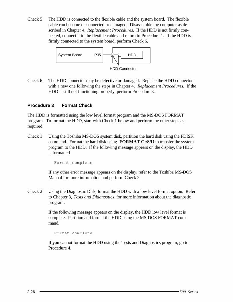
Check 5 The HDD is connected to the flexible cable and the system board. The flexiblecable can become disconnected or damaged. Disassemble the computer as de-scribed in Chapter 4, Replacement Procedures. If the HDD is not firmly con-nected, connect it to the flexible cable and return to Procedure 1. If the HDD isfirmly connected to the system board, perform Check 6.
System Board PJ5 HDD
HDD Connector
Check 6 The HDD connector may be defective or damaged. Replace the HDD connectorwith a new one following the steps in Chapter 4, Replacement Procedures. If theHDD is still not functioning properly, perform Procedure 3.
Procedure 3 Format Check
The HDD is formatted using the low level format program and the MS-DOS FORMATprogram. To format the HDD, start with Check 1 below and perform the other steps asrequired.
Check 1 Using the Toshiba MS-DOS system disk, partition the hard disk using the FDISKcommand. Format the hard disk using FORMAT C:/S/U to transfer the systemprogram to the HDD. If the following message appears on the display, the HDDis formatted.
Format complete
If any other error message appears on the display, refer to the Toshiba MS-DOSManual for more information and perform Check 2.
Check 2 Using the Diagnostic Disk, format the HDD with a low level format option. Referto Chapter 3, Tests and Diagnostics, for more information about the diagnosticprogram.
If the following message appears on the display, the HDD low level format iscomplete. Partition and format the HDD using the MS-DOS FORMAT com-mand.
Format complete
If you cannot format the HDD using the Tests and Diagnostics program, go toProcedure 4.
500 Series 2-27
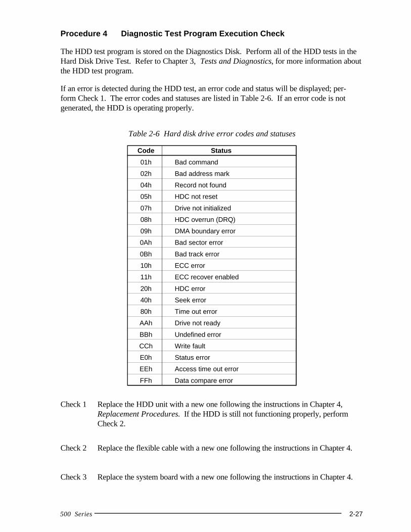
Procedure 4 Diagnostic Test Program Execution Check
The HDD test program is stored on the Diagnostics Disk. Perform all of the HDD tests in theHard Disk Drive Test. Refer to Chapter 3, Tests and Diagnostics, for more information aboutthe HDD test program.
If an error is detected during the HDD test, an error code and status will be displayed; per-form Check 1. The error codes and statuses are listed in Table 2-6. If an error code is notgenerated, the HDD is operating properly.
Table 2-6 Hard disk drive error codes and statuses
Code Status
01h Bad command
02h Bad address mark
04h Record not found
05h HDC not reset
07h Drive not initialized
08h HDC overrun (DRQ)
09h DMA boundary error
0Ah Bad sector error
0Bh Bad track error
10h ECC error
11h ECC recover enabled
20h HDC error
40h Seek error
80h Time out error
AAh Drive not ready
BBh Undefined error
CCh Write fault
E0h Status error
EEh Access time out error
FFh Data compare error
Check 1 Replace the HDD unit with a new one following the instructions in Chapter 4,Replacement Procedures. If the HDD is still not functioning properly, performCheck 2.
Check 2 Replace the flexible cable with a new one following the instructions in Chapter 4.
Check 3 Replace the system board with a new one following the instructions in Chapter 4.
2-28 500 Series
2.7 Keyboard Troubleshooting
To determine if the keyboard is functioning properly, perform the following procedures. Startwith Procedure 1 and continue with the other procedure as instructed.
Procedure 1: Diagnostic Test Program Execution Check
Procedure 2: Connector and Replacement Check
Procedure 1 Diagnostic Test Program Execution Check
Execute the Keyboard Test in the Diagnostic Program. Refer to Chapter 3, Tests and Diag-nostics, for more information on how to perform the test program.
If an error occurs, go to Procedure 2. If an error does not occur, the keyboard is functioningproperly.
Procedure 2 Connector and Replacement Check
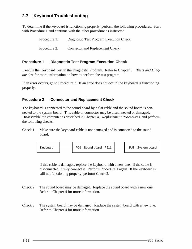
The keyboard is connected to the sound board by a flat cable and the sound board is con-nected to the system board. This cable or connector may be disconnected or damaged.Disassemble the computer as described in Chapter 4, Replacement Procedures, and performthe following checks:
Check 1 Make sure the keyboard cable is not damaged and is connected to the soundboard.
Keyboard PJ9 Sound board PJ11 PJ8 System board
If this cable is damaged, replace the keyboard with a new one. If the cable isdisconnected, firmly connect it. Perform Procedure 1 again. If the keyboard isstill not functioning properly, perform Check 2.
Check 2 The sound board may be damaged. Replace the sound board with a new one.Refer to Chapter 4 for more information.
Check 3 The system board may be damaged. Replace the system board with a new one.Refer to Chapter 4 for more information.
500 Series 2-29
2.8 Display Troubleshooting
This section describes how to determine if the display is functioning properly. Start withProcedure 1 and continue with the other procedures as instructed.
Procedure 1: External Monitor Check
Procedure 2: Diagnostic Test Program Execution Check
Procedure 3: Connector Check
Procedure 4: Replacement Check
Procedure 1 External Monitor Check
Connect the external monitor to the computer’s external monitor port, then boot the com-puter. The computer automatically detects the external monitor even if Resume mode isenabled.
If the external monitor works correctly, the internal LCD display may be damaged. Go toProcedure 3.
If the external monitor appears to have the same problem as the internal LCD, the displaycontroller may be damaged. Go to Procedure 2.
Procedure 2 Diagnostic Test Program Execution Check
The Display Test program is stored on the computer Diagnostic Disk. This program checksthe display controller on the system board. Insert the Diagnostics disk in the floppy diskdrive, turn on the computer, and run the test. Refer to Chapter 3, Tests and Diagnostics, fordetails.
If an error is detected, go to Procedure 3. If an error is not detected, the display is function-ing properly.
2-30 500 Series
Procedure 3 Connector Check
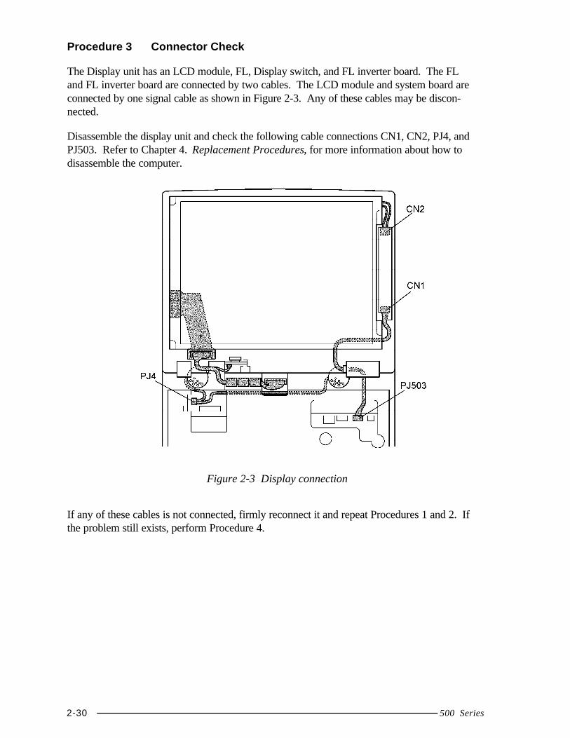
The Display unit has an LCD module, FL, Display switch, and FL inverter board. The FLand FL inverter board are connected by two cables. The LCD module and system board areconnected by one signal cable as shown in Figure 2-3. Any of these cables may be discon-nected.
Disassemble the display unit and check the following cable connections CN1, CN2, PJ4, andPJ503. Refer to Chapter 4. Replacement Procedures, for more information about how todisassemble the computer.
Figure 2-3 Display connection
If any of these cables is not connected, firmly reconnect it and repeat Procedures 1 and 2. Ifthe problem still exists, perform Procedure 4.
500 Series 2-31
Procedure 4 Replacement Check
The FL, FL inverter board, LCD module, and PCI board are connected to the display circuits.Any of these components may be damaged. Refer to Chapter 4, Replacement Procedures, forinstructions on how to disassemble the computer and then perform the following checks:
If the FL does not light, perform Check 1.
If characters are not displayed clearly, perform Check 3.
If some screen functions do not operate properly, perform Check 3.
If the FL remains lit when the display is closed, perform Check 4.
Check 1 Replace the FL inverter board with a new one and test the display again. If theproblem still exists, perform Check 2.
Check 2 Replace the FL with a new one and test the display again. If the problem stillexists, perform Check 3.
Check 3 Replace the LCD module with a new one and test the display again. If theproblem still exists, perform Check 4.
Check 4 Replace the display switch with a new one and test the display again. If theproblem still exists, perform Check 5.
Check 5 Replace the display cable with a new one and test the display again. If theproblem still exists, perform Check 6.
Check 6 The PCI board may be damaged. Replace the PCI board with a new one.
2-32 500 Series
2.9 CD-ROM Drive Troubleshooting
This section describes how to determine if the CD-ROM drive is functioning properly. Per-form the steps below starting with Procedure 1 and continuing with the other procedures asrequired.
Procedure 1: CD Cleaning Check
Procedure 2: Diagnostic Test Program Execution Check
Procedure 3: Connector Check and Replacement Check
Procedure 1 CD Cleaning Check
1. Turn off the power.
2. Open the CD drawer by inserting a slender object such as a straightened paper clipinto the eject hole. The object must be long enough to activate the eject mecha-nism.
3. Clean the laser pickup lens with a lens cleaner. Apply the cleaner to a cloth andwipe the lens.
4. If the CD-ROM drive still does not function properly after cleaning, go to Proce-dure 2.
Procedure 2 Diagnostic Test Program Execution Check
The CD-ROM drive Diagnostic test program is stored on the Diagnostics Disk. Insert a testCD (Toshiba-EMI Test Disc TDY-03) into the CD-ROM drive. Then insert the Diagnosticsdisk into the floppy disk drive, turn on the computer, and run the test. Refer to Chapter 3,Tests and Diagnostics, for more information about the diagnostics test procedures.
If any other errors occur while executing the CD-ROM drive diagnostics test, go to Proce-dure 3.
500 Series 2-33
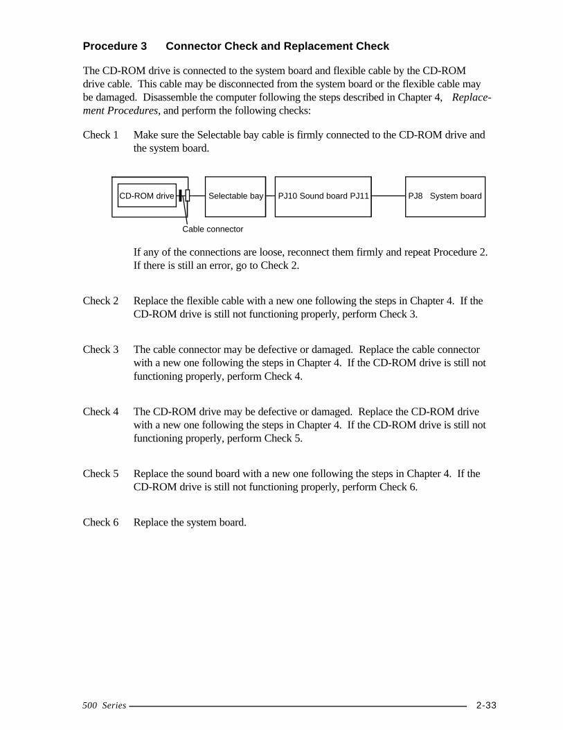
Procedure 3 Connector Check and Replacement Check
The CD-ROM drive is connected to the system board and flexible cable by the CD-ROMdrive cable. This cable may be disconnected from the system board or the flexible cable maybe damaged. Disassemble the computer following the steps described in Chapter 4, Replace-ment Procedures, and perform the following checks:
Check 1 Make sure the Selectable bay cable is firmly connected to the CD-ROM drive andthe system board.
CD-ROM drive Selectable bay PJ10 Sound board PJ11 PJ8 System board
Cable connector
If any of the connections are loose, reconnect them firmly and repeat Procedure 2.If there is still an error, go to Check 2.
Check 2 Replace the flexible cable with a new one following the steps in Chapter 4. If theCD-ROM drive is still not functioning properly, perform Check 3.
Check 3 The cable connector may be defective or damaged. Replace the cable connectorwith a new one following the steps in Chapter 4. If the CD-ROM drive is still notfunctioning properly, perform Check 4.
Check 4 The CD-ROM drive may be defective or damaged. Replace the CD-ROM drivewith a new one following the steps in Chapter 4. If the CD-ROM drive is still notfunctioning properly, perform Check 5.
Check 5 Replace the sound board with a new one following the steps in Chapter 4. If theCD-ROM drive is still not functioning properly, perform Check 6.
Check 6 Replace the system board.
2-34 500 Series
2.10 Internal Modem Troubleshooting
This section describes how to determine if the computer’s internal modem is functioningproperly. Perform the steps below starting with Procedure 1 and continuing with the otherprocedure as required.
Procedure 1: Diagnostic Test Program Execution Check
Procedure 2: Connector Check and Replacement Check
Procedure 1 Diagnostic Test Program Execution Check
The internal modem Diagnostic test program is stored on the Diagnostic Disk. This programchecks the internal modem. Insert the Diagnostics disk into the floppy disk drive, turn on thecomputer, and run the test. Refer to Chapter 3, Tests and Diagnostics, for details.
Check 1 Execute modem test 1. If an error occurs, the modem board may be malfunction-ing. Replace the modem board. If errors still occur, go to Check 2.
Check 2 Execute modem test 3. If an error occurs, the DAA module may be malfunction-ing. Replace the DAA module. If errors still occur, go to Check 3.
Check 3 Execute modem test 2. If an error occurs, the modem board and DAA modulemay be malfunctioning. Replace both.
If any other errors occur while executing the internal modem diagnostics test, go to Procedure2.
Procedure 2 Connector Check and Replacement Check
The DAA board is connected to the modem board. If the modem malfunctions, there may bea bad connection between the DAA board and the modem board or between the modem boardand the PCI board or the DAA module, modem board, or PCI board might be damaged.Disassemble the computer following the steps described in Chapter 4, Replacement Proce-dures, and perform the following checks:
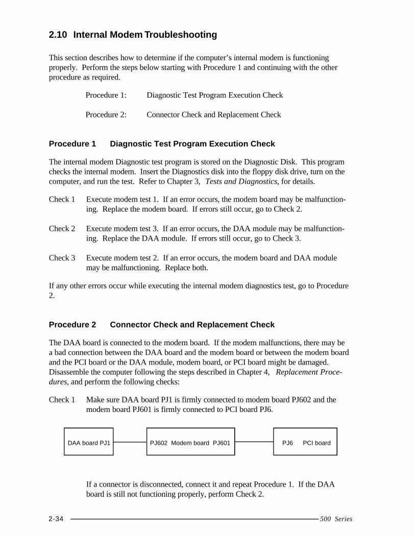
Check 1 Make sure DAA board PJ1 is firmly connected to modem board PJ602 and themodem board PJ601 is firmly connected to PCI board PJ6.
DAA board PJ1 PJ602 Modem board PJ601 PJ6 PCI board
If a connector is disconnected, connect it and repeat Procedure 1. If the DAAboard is still not functioning properly, perform Check 2.
500 Series 2-35
Check 2 The DAA board may be defective or damaged. Replace the DAA board with anew one following the steps in Chapter 4. If the DAA board is still not function-ing properly, perform Check 3.
Check 3 Replace the modem board with a new one following the steps in Chapter 4. If theDAA board is still not functioning properly, perform Check 4.
Check 4 Replace the PCI board with a new one following the steps in Chapter 4.
500 Series 3-1
3.1 The Diagnostic Test
This chapter explains how to use the Diagnostic Test program to test the functions of thecomputer’s hardware modules. The Diagnostics Program is stored on the Diagnostic Diskand consists of 9 programs that are grouped into the Service Program Module (DIAGNOS-TICS MENU).
NOTES: To start the diagnostics, follow these steps:1. Check all cables for loose connections.2. Exit any application you may be using and close Windows.
The DIAGNOSTICS MENU consists of the following nine functions.
❑ DIAGNOSTIC TEST❑ HARD DISK FORMAT❑ HEAD CLEANING❑ LOG UTILITIES❑ RUNNING TEST❑ FDD UTILITIES❑ SYSTEM CONFIGURATION❑ EXIT TO MS-DOS❑ SETUP
3-2 500 Series
The DIAGNOSTIC TEST MENU contains the following functional tests:
❑ SYSTEM TEST❑ MEMORY TEST❑ KEYBOARD TEST❑ DISPLAY TEST❑ FLOPPY DISK TEST❑ PRINTER TEST❑ ASYNC TEST❑ HARD DISK TEST❑ REAL TIMER TEST❑ NDP TEST❑ EXPANSION TEST❑ SOUND TEST❑ CD-ROM TEST❑ MODEM TEST
You will need the following equipment to perform some of the Diagnostic test programs.
❑ The Diagnostics Disk (all tests)❑ A formatted working disk for the floppy disk drive test (all tests)❑ An external FDD attachment❑ A cleaning kit to clean the floppy disk drive heads (Head Cleaning)❑ A PC card wraparound connector for the I/O card test (PCMCIA test)❑ A printer wraparound connector for the printer wraparound test (Printer test)❑ An RS-232-C wraparound connector for the RS-232-C port wraparound test
(ASYNC test)❑ A CD test media (Toshiba-EMI test disk TDY-03 and music CD) (CD-ROM test)❑ External CRT (All tests)❑ PS/2 or compatible keyboard (All tests)❑ PS/2 or compatible mouse (Keyboard test)❑ Serial port wraparound connector (ASYNC test)❑ Multimedia sound system with line-in and line-out ports (Sound test)❑ Headphone (Sound test)❑ CD-ROM drive (CD-ROM test)❑ A telephone❑ A microphone❑ An external speaker
The following sections detail the tests within the Diagnostic Test functions of the DIAGNOS-TIC TEST MENU. Refer to Sections 3.20 through 3.26 for detailed information on theremaining Service Program Module functions.
500 Series 3-3
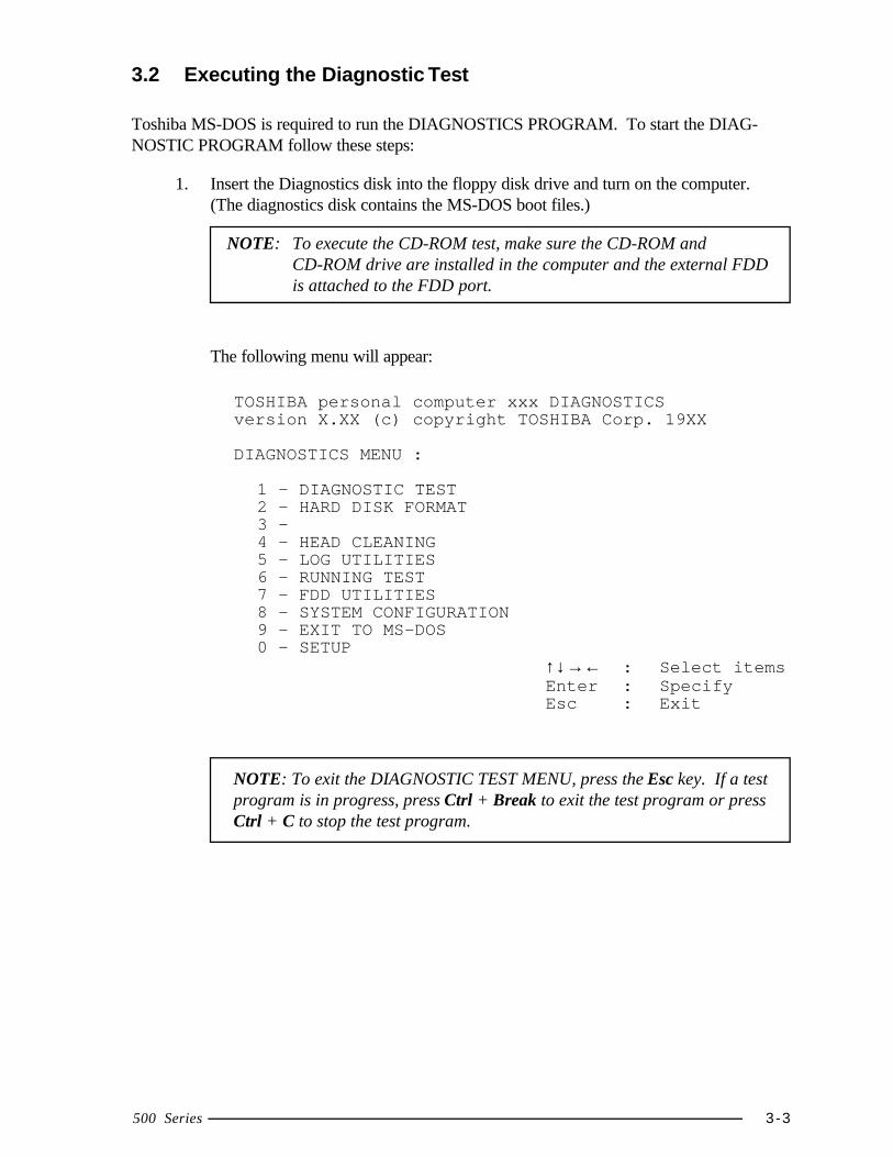
3.2 Executing the Diagnostic Test
Toshiba MS-DOS is required to run the DIAGNOSTICS PROGRAM. To start the DIAG-NOSTIC PROGRAM follow these steps:
1. Insert the Diagnostics disk into the floppy disk drive and turn on the computer.(The diagnostics disk contains the MS-DOS boot files.)
NOTE: To execute the CD-ROM test, make sure the CD-ROM andCD-ROM drive are installed in the computer and the external FDDis attached to the FDD port.
The following menu will appear:
TOSHIBA personal computer xxx DIAGNOSTICSversion X.XX (c) copyright TOSHIBA Corp. 19XX
DIAGNOSTICS MENU :
1 - DIAGNOSTIC TEST2 - HARD DISK FORMAT3 -4 - HEAD CLEANING5 - LOG UTILITIES6 - RUNNING TEST7 - FDD UTILITIES8 - SYSTEM CONFIGURATION9 - EXIT TO MS-DOS0 - SETUP
↑↓→← : Select itemsEnter : SpecifyEsc : Exit
NOTE: To exit the DIAGNOSTIC TEST MENU, press the Esc key. If a testprogram is in progress, press Ctrl + Break to exit the test program or pressCtrl + C to stop the test program.
3-4 500 Series
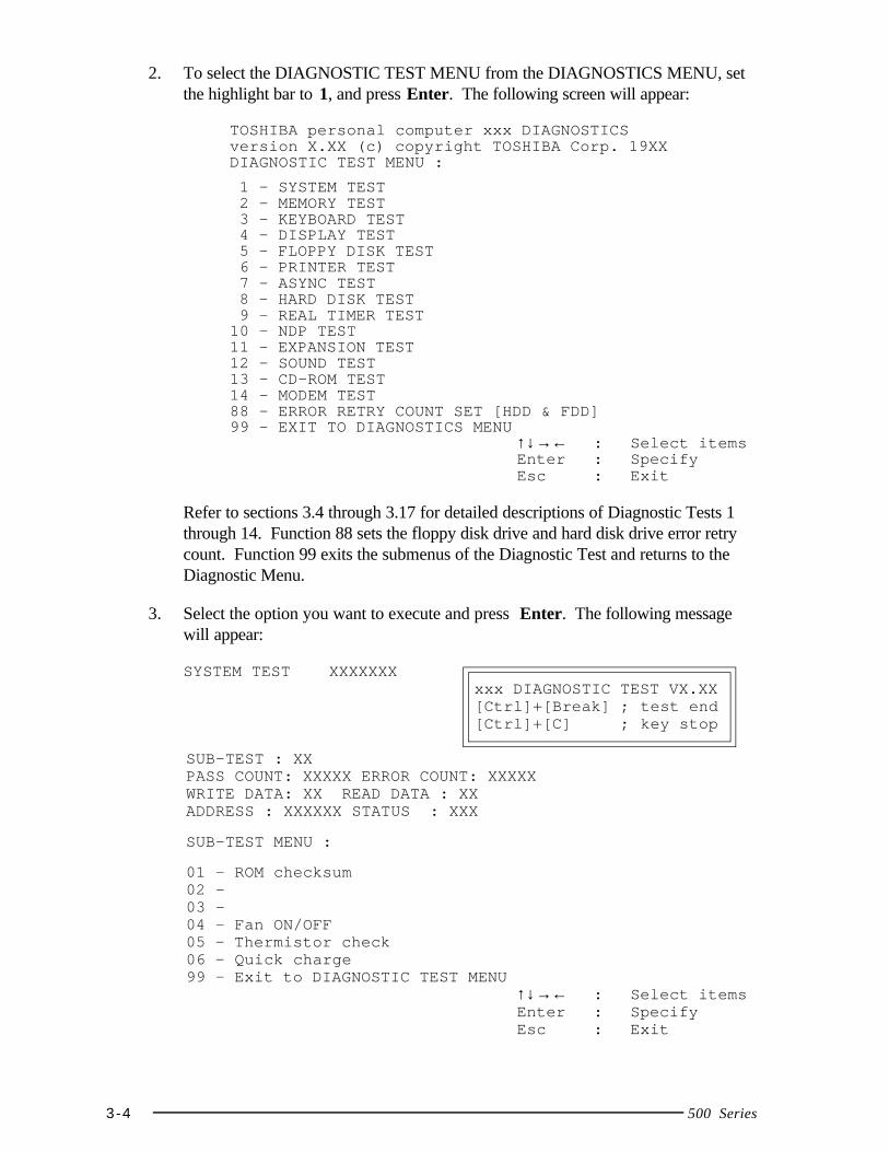
2. To select the DIAGNOSTIC TEST MENU from the DIAGNOSTICS MENU, setthe highlight bar to 1, and press Enter. The following screen will appear:
TOSHIBA personal computer xxx DIAGNOSTICSversion X.XX (c) copyright TOSHIBA Corp. 19XXDIAGNOSTIC TEST MENU :
1 - SYSTEM TEST 2 - MEMORY TEST 3 - KEYBOARD TEST 4 - DISPLAY TEST 5 - FLOPPY DISK TEST 6 - PRINTER TEST 7 - ASYNC TEST 8 - HARD DISK TEST 9 - REAL TIMER TEST10 - NDP TEST11 - EXPANSION TEST12 - SOUND TEST13 - CD-ROM TEST14 - MODEM TEST88 - ERROR RETRY COUNT SET [HDD & FDD]99 - EXIT TO DIAGNOSTICS MENU
↑↓→← : Select itemsEnter : SpecifyEsc : Exit
Refer to sections 3.4 through 3.17 for detailed descriptions of Diagnostic Tests 1through 14. Function 88 sets the floppy disk drive and hard disk drive error retrycount. Function 99 exits the submenus of the Diagnostic Test and returns to theDiagnostic Menu.
3. Select the option you want to execute and press Enter. The following messagewill appear:
SYSTEM TEST XXXXXXXxxx DIAGNOSTIC TEST VX.XX[Ctrl]+[Break] ; test end[Ctrl]+[C] ; key stop
SUB-TEST : XXPASS COUNT: XXXXX ERROR COUNT: XXXXXWRITE DATA: XX READ DATA : XXADDRESS : XXXXXX STATUS : XXX
SUB-TEST MENU :
01 - ROM checksum02 -03 -04 - Fan ON/OFF05 - Thermistor check06 - Quick charge99 - Exit to DIAGNOSTIC TEST MENU
↑↓→← : Select itemsEnter : SpecifyEsc : Exit
500 Series 3-5
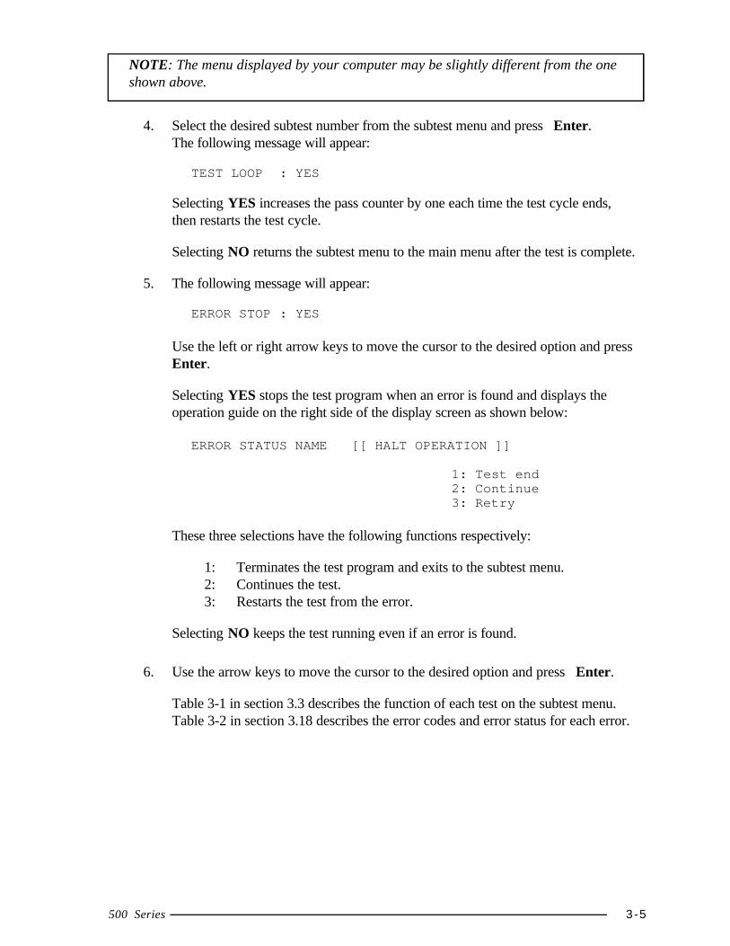
NOTE: The menu displayed by your computer may be slightly different from the oneshown above.
4. Select the desired subtest number from the subtest menu and press Enter.The following message will appear:
TEST LOOP : YES
Selecting YES increases the pass counter by one each time the test cycle ends,then restarts the test cycle.
Selecting NO returns the subtest menu to the main menu after the test is complete.
5. The following message will appear:
ERROR STOP : YES
Use the left or right arrow keys to move the cursor to the desired option and pressEnter.
Selecting YES stops the test program when an error is found and displays theoperation guide on the right side of the display screen as shown below:
ERROR STATUS NAME [[ HALT OPERATION ]]
1: Test end2: Continue3: Retry
These three selections have the following functions respectively:
1: Terminates the test program and exits to the subtest menu.2: Continues the test.3: Restarts the test from the error.
Selecting NO keeps the test running even if an error is found.
6. Use the arrow keys to move the cursor to the desired option and press Enter.
Table 3-1 in section 3.3 describes the function of each test on the subtest menu.Table 3-2 in section 3.18 describes the error codes and error status for each error.
3-6 500 Series
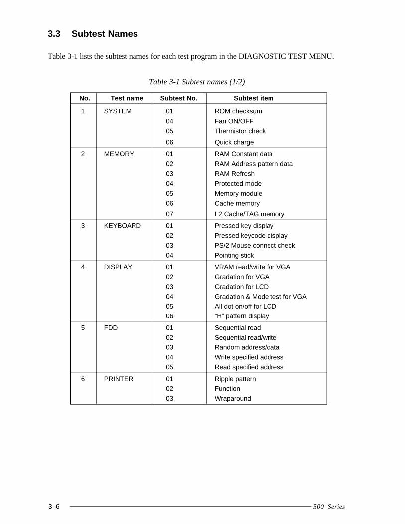
3.3 Subtest Names
Table 3-1 lists the subtest names for each test program in the DIAGNOSTIC TEST MENU.
Table 3-1 Subtest names (1/2)
No. Test name Subtest No. Subtest item
1 SYSTEM 01 ROM checksum
04 Fan ON/OFF
05 Thermistor check
06 Quick charge
2 MEMORY 01 RAM Constant data
02 RAM Address pattern data
03 RAM Refresh
04 Protected mode
05 Memory module
06 Cache memory
07 L2 Cache/TAG memory
3 KEYBOARD 01 Pressed key display
02 Pressed keycode display
03 PS/2 Mouse connect check
04 Pointing stick
4 DISPLAY 01 VRAM read/write for VGA
02 Gradation for VGA
03 Gradation for LCD
04 Gradation & Mode test for VGA
05 All dot on/off for LCD
06 “H” pattern display
5 FDD 01 Sequential read
02 Sequential read/write
03 Random address/data
04 Write specified address
05 Read specified address
6 PRINTER 01 Ripple pattern
02 Function
03 Wraparound
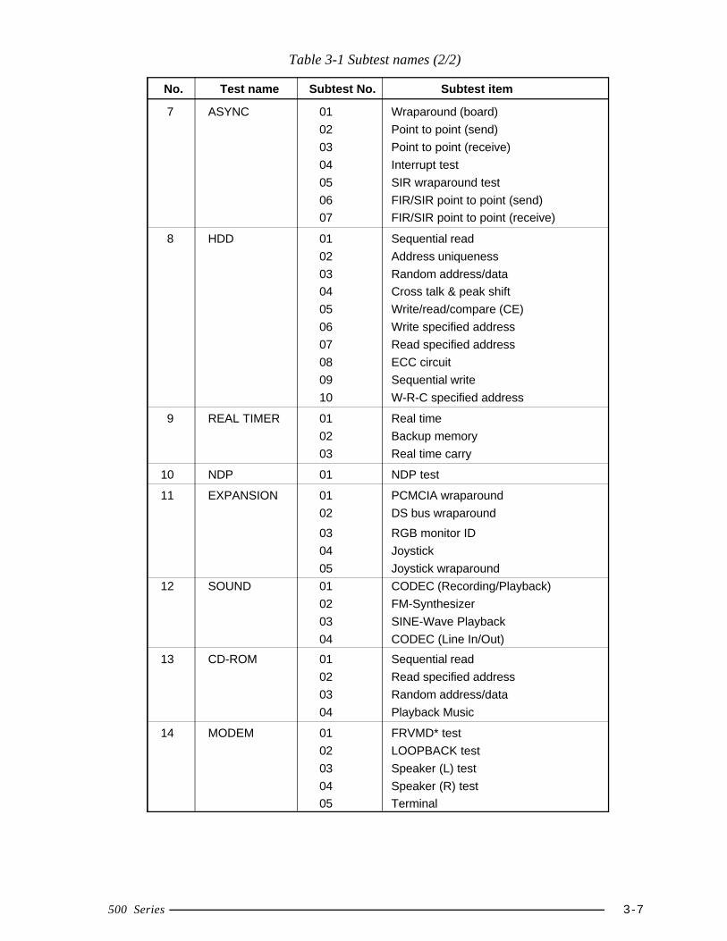
500 Series 3-7
Table 3-1 Subtest names (2/2)
No. Test name Subtest No. Subtest item
7 ASYNC 01 Wraparound (board)
02 Point to point (send)
03 Point to point (receive)
04 Interrupt test
05 SIR wraparound test
06 FIR/SIR point to point (send)
07 FIR/SIR point to point (receive)
8 HDD 01 Sequential read
02 Address uniqueness
03 Random address/data
04 Cross talk & peak shift
05 Write/read/compare (CE)
06 Write specified address
07 Read specified address
08 ECC circuit
09 Sequential write
10 W-R-C specified address
9 REAL TIMER 01 Real time
02 Backup memory
03 Real time carry
10 NDP 01 NDP test
11 EXPANSION 01 PCMCIA wraparound
02 DS bus wraparound
03 RGB monitor ID
04 Joystick
05 Joystick wraparound
12 SOUND 01 CODEC (Recording/Playback)
02 FM-Synthesizer
03 SINE-Wave Playback
04 CODEC (Line In/Out)
13 CD-ROM 01 Sequential read
02 Read specified address
03 Random address/data
04 Playback Music
14 MODEM 01 FRVMD* test
02 LOOPBACK test
03 Speaker (L) test
04 Speaker (R) test
05 Terminal
3-8 500 Series
3.4 System Test
To execute the System Test select 1 from the DIAGNOSTIC TEST MENU, press Enter, andfollow the directions displayed on the screen. Move the highlight bar to the subtest you wantto execute and press Enter.
Subtest 01 ROM checksum
This subtest executes a checksum test of the BIOS ROM on the system board.
Subtest 02 Not used
Subtest 03 Not used
Subtest 04 Fan on/off
This subtest checks fan operation using the on/off command.
The fan cable is securely connected to the system board. When you executethis subtest, the following message is displayed:
*** Fan ON *** : Press [Enter] key?
When you press Enter, the fan should spin.
*** Fan OFF *** : Press [Enter] key?
When you press Enter, the fan should stop.
Subtest 05 Thermistor check
This subtest reads the thermistor connect check status of the power supplymicroprocessor, then compares it with the original data. If the data indicatesthe connector is open or shorted, it displays an error message.
Subtest 06 Quick charge
Displays quick-charge status.
500 Series 3-9
3.5 Memory Test
To execute the Memory Test select 2 from the DIAGNOSTIC TEST MENU, press Enter,and follow the directions displayed on the screen. Move the highlight bar to the subtest youwant to execute and press Enter.
Subtest 01 Constant data (real mode)
This subtest writes a 256-byte unit of constant data to conventional memory(0 to 640 KB), then reads the new data and compares the result with theoriginal data. The constant data is FFFFh, AAAAh, 5555h, and 0000h.
Subtest 02 Address pattern data (real mode)
This subtest writes address pattern data created by the exclusive-ORing(XORing) to the address segment and address offset in conventional memoryprogram end to 640 KB, then reads the new data and compares the result withthe original data.
Subtest 03 Refresh (real mode)
This subtest writes a 256-byte unit of constant data to conventional memory(0 to 640 KB) then reads the new data and compares the result with the origi-nal data.
The constant data is AAAAh and 5555h.
NOTE: There is a short delay between write and read operations, de-pending on the size of the data.
Subtest 04 Protected mode
NOTE: The CONFIG.SYS file must be configured without expandedmemory manager programs such as EMM386.EXE, EMM386.SYS orQEMM386.SYS. Also, the HIMEM.SYS must be deleted from theCONFIG.SYS file.
This subtest writes constant data and address data to extended memory (maxi-mum address 100000h) then reads new data and compares the result with theoriginal data.
The constant data is FFh, AAh, 55h, and 00h.
3-10 500 Series
Subtest 05 Memory module
NOTE: To execute this subtest, an optional memory card must be in-stalled in the computer.
This subtest functions the same as subtest 04, except it is used for testing anoptional memory card. Memory module capacity is 8 MB, 16 MB, 32 MB, 48MB, and 128 MB.
After selecting subtest 05, the following message will appear:
Extended memory size(1:8 MB,2:16 MB,3:32 MB,4:48 MB,5:128 MB)?
Select the number that corresponds to the memory card installed in the com-puter.
Subtest 06 Cache memory
To test the cache memory, a pass-through write-read comparison of ‘5A’ datais run repeatedly to the test area (‘7000’:’Program’ size to ‘7000’:’7FFF’ (32KB)) to check the hit-miss ratio (on/off status) for CPU cache memory. Onetest takes 3 seconds.
Number of misses < Number of hits → OKNumber of misses ≥ Number of hits → Fail
Subtest 07 L2 Cache memory
To test the cache memory, a pass-through write-read comparison of ‘5A’ datais run repeatedly to the test area (‘7000’:’Program’ size to ‘7000’:’7FFF’ (32KB)) to check the hit-miss ratio (on/off status) for L2 cache memory. One testtakes 3 seconds.
Number of misses < Number of hits → OKNumber of misses ≥ Number of hits → Fail
500 Series 3-11
3.6 Keyboard Test
To execute the Keyboard Test select 3 from the DIAGNOSTIC TEST MENU, press Enter,and follow the directions displayed on the screen. The Keyboard test contains four subteststhat test the keyboard, PS/2 mouse, and AccuPoint actions. Move the highlight bar to thesubtest you want to execute and press Enter.
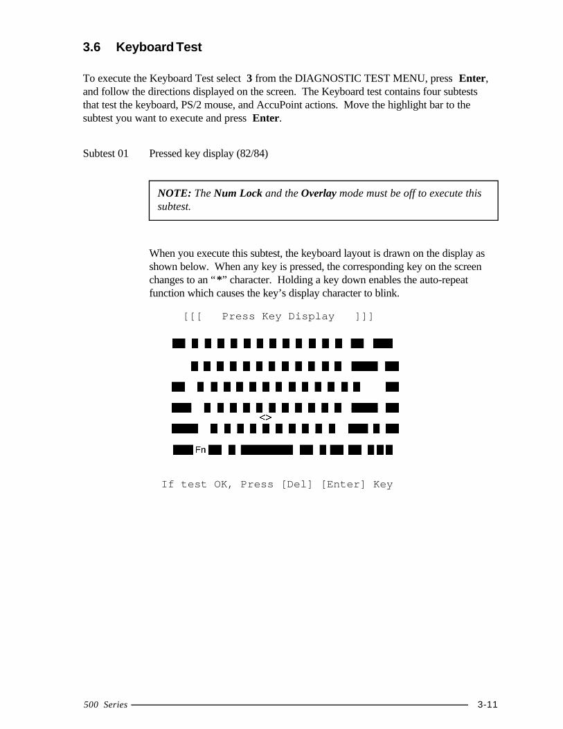
Subtest 01 Pressed key display (82/84)
NOTE: The Num Lock and the Overlay mode must be off to execute thissubtest.
When you execute this subtest, the keyboard layout is drawn on the display asshown below. When any key is pressed, the corresponding key on the screenchanges to an “*” character. Holding a key down enables the auto-repeatfunction which causes the key’s display character to blink.
[[[ Press Key Display ]]]
If test OK, Press [Del] [Enter] Key
3-12 500 Series
Subtest 02 Pressed keycode display
When a key is pressed, the scan code, character code, and keytop name aredisplayed on the screen in the format shown below. The Ins, Caps Lock,Num Lock, Scroll Lock, Alt, Ctrl, Left Shift, and Right Shift keys aredisplayed in reverse screen mode when pressed. The scan codes, charactercodes, and keytop names are shown in Appendix D.
KEYBOARD TEST IN PROGRESS 302000
Scan code = Character code = Keytop =
Ins Lock Caps Lock Num Lock Scroll LockAlt Ctrl Left Shift Right Shift
PRESS [Enter] KEY
Subtest 03 PS/2 mouse connect check
NOTE: To execute the PS/2 mouse connect check, a PS/2 mouse must beconnected to the computer.
This subtest checks whether a PS/2 mouse is connected or not.
If this test does not detect an error, it returns to the subtest menu.If this test detects an error, the following message appears:
KBD - MOUSE INTERFACE ERROR
[[ HALT OPERATION ]]
1: Test end2: Continue3: Retry

500 Series 3-13
Subtest 04 Pointing Stick
This subtest checks the functions of the pointing stick as shown below.
a) IPS stick pressure sensing direction and parameter.b) IPS switch function check.
This test reports the pointing stick motion response from the IPS and IPSswitch. When the stick is pressed towards the upper left, the <POINTING>display changes according to the following illustration. If an IPS switch ispressed, the <BUTTON> display alternates between black and white. Also, theparameters appear on the right side of the display. If two IPS switches arepressed at the same time, the subtest menu is displayed.
***** IPS TEST PROGRAM (V1.00) *****
<< PRESS BUTTON1 + BUTTON2 THEN END >>
When a button is pressed, the display alternates as shown below.
3-14 500 Series
3.7 Display Test
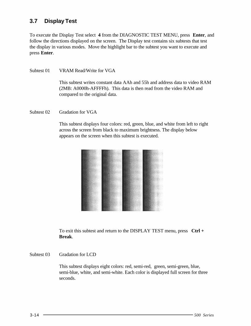
To execute the Display Test select 4 from the DIAGNOSTIC TEST MENU, press Enter, andfollow the directions displayed on the screen. The Display test contains six subtests that testthe display in various modes. Move the highlight bar to the subtest you want to execute andpress Enter.
Subtest 01 VRAM Read/Write for VGA
This subtest writes constant data AAh and 55h and address data to video RAM(2MB: A0000h-AFFFFh). This data is then read from the video RAM andcompared to the original data.
Subtest 02 Gradation for VGA
This subtest displays four colors: red, green, blue, and white from left to rightacross the screen from black to maximum brightness. The display belowappears on the screen when this subtest is executed.
To exit this subtest and return to the DISPLAY TEST menu, press Ctrl +Break.
Subtest 03 Gradation for LCD
This subtest displays eight colors: red, semi-red, green, semi-green, blue,semi-blue, white, and semi-white. Each color is displayed full screen for threeseconds.
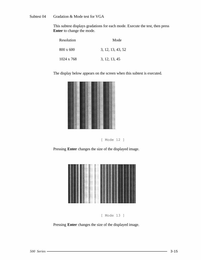
500 Series 3-15
Subtest 04 Gradation & Mode test for VGA
This subtest displays gradations for each mode. Execute the test, then pressEnter to change the mode.
Resolution Mode
800 x 600 3, 12, 13, 43, 52
1024 x 768 3, 12, 13, 45
The display below appears on the screen when this subtest is executed.
[ Mode 12 ]
Pressing Enter changes the size of the displayed image.
[ Mode 13 ]
Pressing Enter changes the size of the displayed image.
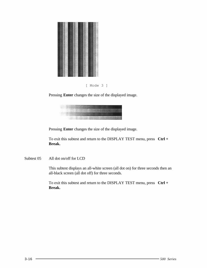
3-16 500 Series
[ Mode 3 ]
Pressing Enter changes the size of the displayed image.
Pressing Enter changes the size of the displayed image.
To exit this subtest and return to the DISPLAY TEST menu, press Ctrl +Break.
Subtest 05 All dot on/off for LCD
This subtest displays an all-white screen (all dot on) for three seconds then anall-black screen (all dot off) for three seconds.
To exit this subtest and return to the DISPLAY TEST menu, press Ctrl +Break.
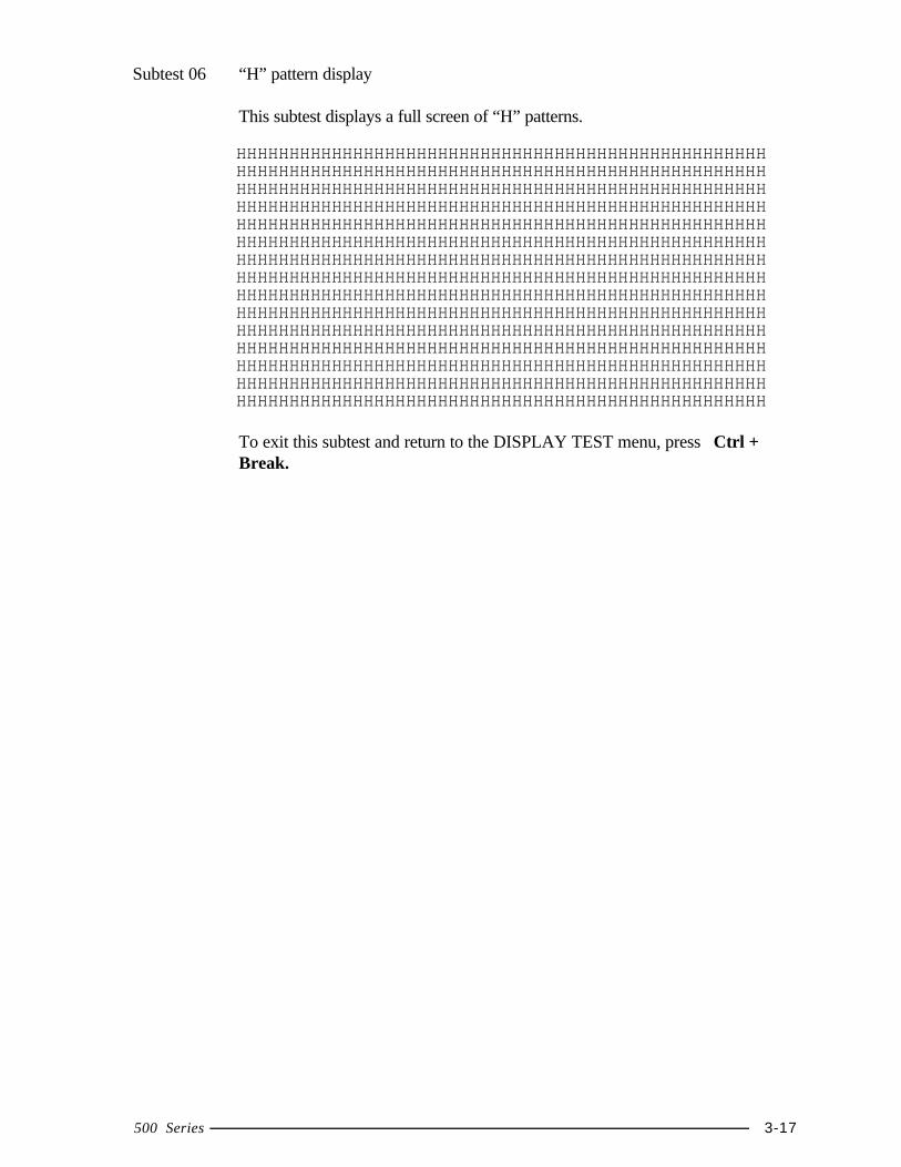
500 Series 3-17
Subtest 06 “H” pattern display
This subtest displays a full screen of “H” patterns.
HHHHHHHHHHHHHHHHHHHHHHHHHHHHHHHHHHHHHHHHHHHHHHHHHHHHHHHHHHHHHHHHHHHHHHHHHHHHHHHHHHHHHHHHHHHHHHHHHHHHHHHHHHHHHHHHHHHHHHHHHHHHHHHHHHHHHHHHHHHHHHHHHHHHHHHHHHHHHHHHHHHHHHHHHHHHHHHHHHHHHHHHHHHHHHHHHHHHHHHHHHHHHHHHHHHHHHHHHHHHHHHHHHHHHHHHHHHHHHHHHHHHHHHHHHHHHHHHHHHHHHHHHHHHHHHHHHHHHHHHHHHHHHHHHHHHHHHHHHHHHHHHHHHHHHHHHHHHHHHHHHHHHHHHHHHHHHHHHHHHHHHHHHHHHHHHHHHHHHHHHHHHHHHHHHHHHHHHHHHHHHHHHHHHHHHHHHHHHHHHHHHHHHHHHHHHHHHHHHHHHHHHHHHHHHHHHHHHHHHHHHHHHHHHHHHHHHHHHHHHHHHHHHHHHHHHHHHHHHHHHHHHHHHHHHHHHHHHHHHHHHHHHHHHHHHHHHHHHHHHHHHHHHHHHHHHHHHHHHHHHHHHHHHHHHHHHHHHHHHHHHHHHHHHHHHHHHHHHHHHHHHHHHHHHHHHHHHHHHHHHHHHHHHHHHHHHHHHHHHHHHHHHHHHHHHHHHHHHHHHHHHHHHHHHHHHHHHHHHHHHHHHHHHHHHHHHHHHHHHHHHHHHHHHHHHHHHHHHHHHHHHHHHHHHHHHHHHHHHHHHHHHHHHHHHHHHHHHHHHHHHHHHHHHHH
To exit this subtest and return to the DISPLAY TEST menu, press Ctrl +Break.
3-18 500 Series
3.8 Floppy Disk Test
NOTE: Before running the floppy disk test, prepare a formatted work disk. Remove theDiagnostics Disk and insert a work disk into the FDD. The contents of the floppy diskwill be erased.
To execute the Floppy Disk Test select 5 from the DIAGNOSTIC TEST MENU, pressEnter, and follow the directions displayed on the screen. The Floppy Disk test contains fivesubtests that test the FDD. The following messages will appear after selecting the FloppyDisk Test from the DIAGNOSTIC TEST MENU. Answer each question with an appropriateresponse to execute the test.
1. Select the test drive number of the floppy disk drive to be tested and press Enter.
Test drive number select (1:FDD#1,2:FDD#2,0:FDD1&2) ?
2. Select the media type of the floppy disk in the test drive to be tested, and pressEnter.
Media in drive #X mode (0:2DD,1:2D,2:2D-2HD/2DD,3:2HD) ?
3. Select the track you want the test to start on and press Enter. Simply pressingEnter sets the start track to zero.
Test start track (Enter:0/dd:00-79) ?
4. The floppy disk test menu will appear after you select the start track number.Select the number of the subtest you want to execute and press Enter. Thefollowing message will appear during the floppy disk test.
FLOPPY DISK XXXXXXXxxxx DIAGNOSTIC TEST VX.XX[Ctrl]+[Break] ; test end[Ctrl]+[C] ; key stop
500 Series 3-19
Subtest 01 Sequential Read
This subtest performs a Cyclic Redundancy Check (CRC), that continuouslyreads all the tracks on a floppy disk. The following tracks are read accordingto the media type in the floppy disk drive:
Double-sided, double-density (2D): Tracks 0 to 39.
Double-sided, double-density, double-track (2DD) and double-sided, high-density, double-track (2HD): Tracks 0 to 79.
The start track is specified when the FDD test is started from the DiagnosticTest Menu. Refer to step 3 at the beginning of this section to set the starttrack.
Subtest 02 Sequential Read/Write
This subtest continuously writes data pattern B5ADADh to all the specifiedtracks selected in subtest 01. The data is then read and compared to theoriginal data.
Subtest 03 Random Address/Data
This subtest writes random data to random addresses on all tracks defined insubtest 01. The data is then read and compared to the original data.
Subtest 04 Write Specified Address
This subtest writes specified data to a specified track, head, and address.
Subtest 05 Read Specified Address
This subtest reads data from a specified track, head, and address.
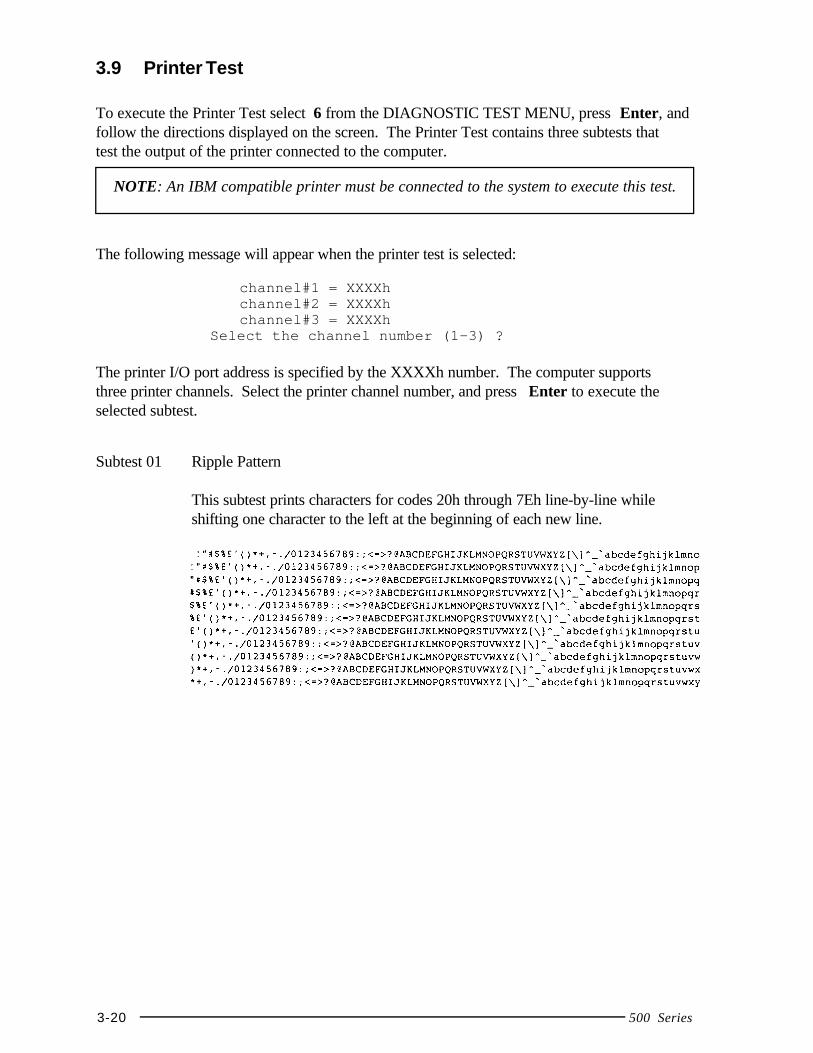
3-20 500 Series
3.9 Printer Test
To execute the Printer Test select 6 from the DIAGNOSTIC TEST MENU, press Enter, andfollow the directions displayed on the screen. The Printer Test contains three subtests thattest the output of the printer connected to the computer.
NOTE: An IBM compatible printer must be connected to the system to execute this test.
The following message will appear when the printer test is selected:
channel#1 = XXXXhchannel#2 = XXXXhchannel#3 = XXXXh
Select the channel number (1-3) ?
The printer I/O port address is specified by the XXXXh number. The computer supportsthree printer channels. Select the printer channel number, and press Enter to execute theselected subtest.
Subtest 01 Ripple Pattern
This subtest prints characters for codes 20h through 7Eh line-by-line whileshifting one character to the left at the beginning of each new line.
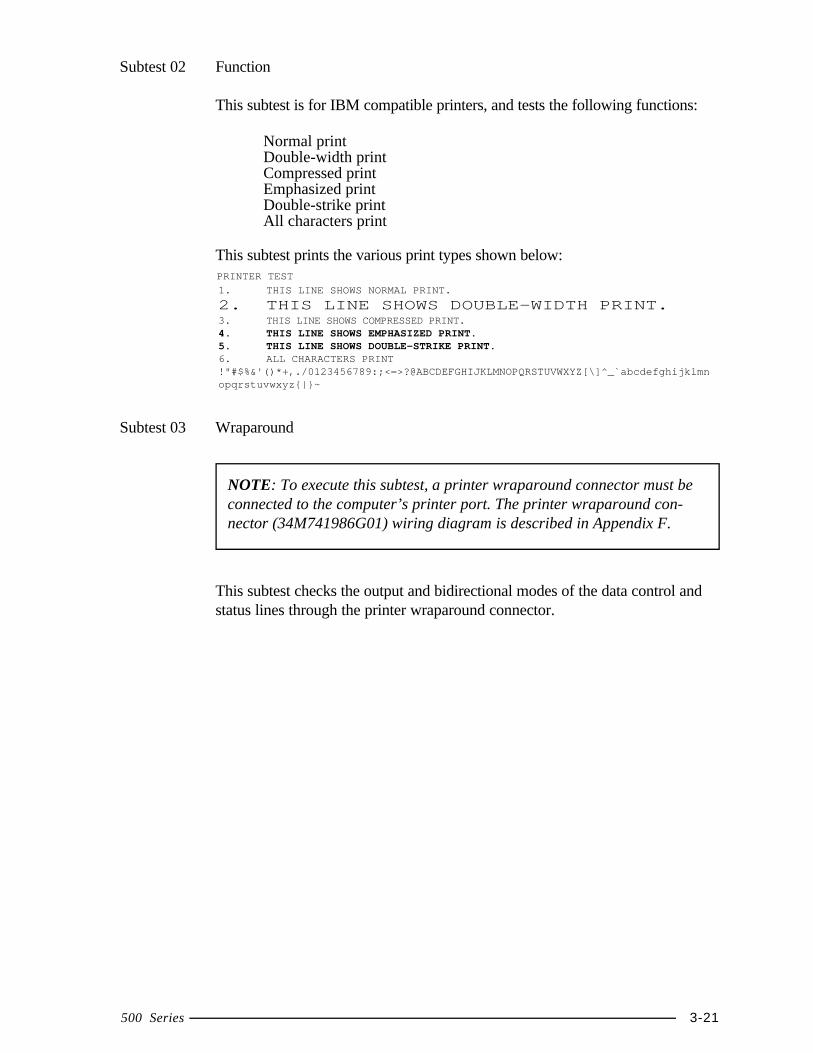
500 Series 3-21
Subtest 02 Function
This subtest is for IBM compatible printers, and tests the following functions:
Normal printDouble-width printCompressed printEmphasized printDouble-strike printAll characters print
This subtest prints the various print types shown below:
Subtest 03 Wraparound
NOTE: To execute this subtest, a printer wraparound connector must beconnected to the computer’s printer port. The printer wraparound con-nector (34M741986G01) wiring diagram is described in Appendix F.
This subtest checks the output and bidirectional modes of the data control andstatus lines through the printer wraparound connector.
PRINTER TEST
1. THIS LINE SHOWS NORMAL PRINT.
2. THIS LINE SHOWS DOUBLE-WIDTH PRINT.3. THIS LINE SHOWS COMPRESSED PRINT.4. THIS LINE SHOWS EMPHASIZED PRINT.5. THIS LINE SHOWS DOUBLE-STRIKE PRINT.6. ALL CHARACTERS PRINT!"#$%&'()*+,./0123456789:;<=>?@ABCDEFGHIJKLMNOPQRSTUVWXYZ[\]^_`abcdefghijklmnopqrstuvwxyz{|}~
3-22 500 Series
3.10 Async Test
To execute the Async Test select 7 from the DIAGNOSTIC TEST MENU, press Enter, andfollow the directions displayed on the screen. The async test contains seven subtests that testthe asynchronous communication functions. Move the highlight bar to the subtest you wantto execute and press Enter.
The subtests require the following data format:
Method: AsynchronousSpeed: 9600BPS (Subtests 01 to 04)
38400BPS (Subtests 05 to 07)Data: 8 bits and one parity bit (EVEN)Data pattern: 20h to 7Eh
The following message will appear at the bottom of the screen when subtests 01, 02, 03, 05,06, and 07 are selected:
Channel#1 = XXXXhChannel#2 = XXXXhChannel#3 = XXXXhSelect the Channel number (1/2/3)
The serial I/O port address is specified by the XXXXh number. Select the serial port channelnumber and press Enter to start the subtest.
Subtest 01 Wraparound (board)
NOTE: To execute this subtest an RS-232-C wraparound connector(34M741621G01) must be connected to the RS-232-C port. The RS-232-C wraparound connector wiring diagram is described in Appendix F.
This subtest checks the data send/receive function through the wraparoundconnector.
Subtest 02 Point to point (Send)
NOTE: To execute this subtest, two machines must be connected with anRS-232-C direct cable. One machine should be set as “send”(subtest 02)and the other set as “receive” (subtest 03). The wiring diagram for theRS-232-C direct cable is described in Appendix F.
This subtest sends 20h through 7Eh data to the receive side, then receives thesent data and compares it to the original data.
500 Series 3-23
Subtest 03 Point to point (Receive)
This subtest is used with subtest 02 described above. This subtest receives thedata from the send side, then sends the received data.
Subtest 04 Interrupt test
This subtest checks the Interrupt Request Level of IRQ 4, 3, and 5 from thesend side.
NOTE: Before conducting subtests 05 to 07, you must executeSIRDRV.COM to enable the infrared communication port.
Subtest 05 SIR Wraparound test
This subtest checks the data send/receive function through the SIR port.
NOTE: To execute subtests 06 and 07, each computer must have accessto the other computer’s infrared port.
Subtest 06 FIR/SIR point to point (Send)
This subtest sends 20h through 7Eh data to the receive side, then receives thesent data and compares it to the original data through the SIR port.
Subtest 07 FIR/SIR point to point (Receive)
This subtest is used with subtest 06 described above. This subtest receives thedata from the send side, then sends the received data through the SIR port.
3-24 500 Series
3.11 Hard Disk Test
To execute the Hard Disk Test select 8 from the DIAGNOSTIC TEST MENU, press Enter,and follow the directions displayed on the screen. The hard disk test contains ten subtests thattest the hard disk drive functions.
NOTE: The contents of the hard disk will be erased when subtest 02, 03, 04, 05, 06,08, 09, or 10 is executed. Before running a test, transfer the contents of thehard disk to a backup system (i.e., floppy disks).1. If MS-DOS 6.22/Windows for Workgroups is selected, use the Master
Diskette Creator (MDC) utility in the Toshiba Utility folder to back up thepreinstalled software. After backing up the preinstalled software, use theBACKUP command in the Toshiba Companion Utility to back up the entiredisk, including the user’s files.
2. If Windows 95 is selected, check to see if the Microsoft Create System DisksTools (MSCSD.EXE) still exists in the System Tools Folder. (This tool canbe used only once.) If it exists, use it to back up the preinstalled software,then use the Backup utility in the System Tools folder to back up the entiredisk, including the user’s files
Refer to the appropriate instructions for each operating system.
1. When you select the hard disk test from the DIAGNOSTIC TEST MENU, thefollowing message will appear:
Test drive number select (1:HDD#1,2:HDD#2,0:HDD1&2) ?
2. Select the hard disk drive number to be tested and press Enter. The followingmessage will appear:
HDC F/W error retry (1:yes,2:no) ?
3. This message is used to select the retry operation when the hard disk controllerdetects an error. Select 1 or 2 and press Enter. The following message willappear:
Data compare error dump (1:no,2:yes) ?
4. This message is used to select the error dump operation when a data compareerror is detected. Select 1 or 2 and press Enter. The following message willappear:
Detail status display (1:no,2:yes) ?5. This message is used to select whether or not the HDD status is displayed on the
screen. The HDD status is described in section 3.19. Select 1 or 2 and pressEnter.
500 Series 3-25
6. The Hard Disk Test message will appear after you respond to the Detail Statusprompt. Select the number of the subtest you want to execute and press Enter.The following message will appear during each subtest.
HARD DISK TEST XXXXXXX
SUB-TEST : XXPASS COUNT: XXXXX ERROR COUNT: XXXXXWRITE DATA: XX READ DATA : XXADDRESS : XXXXXX STATUS : XXX
The first three digits of the ADDRESS indicate which cylinder is being tested, thefourth digit indicates the head and the last two digits indicate the sector.
The first digit of the STATUS number indicates the drive being tested and the lasttwo digits indicate the error status code as explained in Table 3-2.
Subtest 01 Sequential Read
This subtest is a sequential reading of all the tracks on the HDD starting attrack 0. When all the tracks on the HDD have been read, the test starts at themaximum track and reads the tracks on the HDD sequentially back to track 0.
Subtest 02 Address Uniqueness
This subtest writes unique address data to each sector of the HDD track-by-track. The data written to each sector is then read and compared with theoriginal data. There are three ways the HDD can be read:
• Forward sequential• Reverse sequential• Random
Subtest 03 Random Address/Data
This subtest writes random data to random addresses on the HDD cylinder,head, and sector. This data is then read and compared to the original data.
3-26 500 Series
Subtest 04 Cross Talk & Peak Shift
This subtest writes eight types of worst pattern data (shown below) to acylinder, then reads the data while moving from cylinder to cylinder.
Worst pattern data Cylinder
‘B5ADAD’ 0 cylinder
‘4A5252’ 1 cylinder
‘EB6DB6’ 2 cylinder
‘149249’ 3 cylinder
’63B63B’ 4 cylinder
‘9C49C4’ 5 cylinder
‘2DB6DB’ 6 cylinder
‘D24924’ 7 cylinder
Subtest 05 Write/read/compare (CE)
This subtest writes B5ADADh worst pattern data to the CE cylinder on theHDD, then reads the data from the CE cylinder and compares it with theoriginal data.
Subtest 06 Write specified address
This subtest writes specified data to a specified cylinder and head on the HDD.
Subtest 07 Read specified address
This subtest reads data which has been written to a specified cylinder and headon the HDD.
Subtest 08 ECC circuit
This subtest checks the Error Check and Correction (ECC) circuit functions ofthe specified cylinder and head on the HDD.
Subtest 09 Sequential write
This subtest writes specified 2-byte data to all of the cylinders on the HDD.
Subtest 10 W-R-C specified address
This subtest writes data to a specified cylinder and head on the HDD, thenreads the data and compares it to the original data.
500 Series 3-27
3.12 Real Timer Test
To execute the Real Timer Test select 9 from the DIAGNOSTIC TEST MENU, press Enter,and follow the directions on the screen. The real timer test contains three subtests that testthe computer’s real timer functions. Move the highlight bar to the subtest you want to ex-ecute and press Enter.
Subtest 01 Real Time
A new date and time can be input during this subtest. To execute the real timesubtest follow these steps:
1. Select subtest 01 and the following message will appear:
Current date : XX-XX-XXXX Current time : XX:XX:XX
Enter new date:
PRESS [ENTER] KEY TO EXIT TEST
2. If the current date is not correct, input the correct date at the “Enter newdate” prompt and press Enter. The following prompt will appear:
Enter new time :
3. If the current time is not correct, input the correct time in 24-hour format.
Pressing Enter toggles between the time and the date. To exit, press Ctrl+ Break.
Subtest 02 Backup Memory
This subtest performs the following backup memory check:
Writes 1-bit of “on” data to address 01h through 80hWrites 1-bit of “off” data to address 0Eh through 80hWrites the data pattern AAh and 55h to the RTC 114-byte memory(address 0Eh to 7Fh)
The subtest reads and compares this data with the original data.
To exit, press Ctrl + Break.

3-28 500 Series
Subtest 03 Real Time Carry
CAUTION: When this subtest is executed, the current date and time areerased.
This subtest checks the real time clock increments, making sure the date andtime are displayed in the following format:
Current date : 12-31-1995Current time : 23:59:58
Pressing Enter displays the following :
Current date : 01-01-1996Current time : 00:00:00
PRESS [Enter] KEY TO EXIT TEST
Press Ctrl + Break to exit.
500 Series 3-29
3.13 NDP Test
To execute the NDP test select 10 from the DIAGNOSTICS TEST MENU, press Enter, andfollow the directions on the screen. The NDP test contains one subtest that tests the NDPfunctions.
Subtest 01 NDP
This test checks the following functions of NDP:
❑ Control word❑ Status word❑ Bus❑ Addition❑ Multiplication
Press Ctrl + Break to exit.
3-30 500 Series
3.14 Expansion Test
To execute the expansion test select 11 from the DIAGNOSTICS TEST MENU, pressEnter, and follow the directions on the screen. The expansion test contains one subtest.
NOTE: To execute this subtest, the PC card wraparound connector is required.
Subtest 01 PCMCIA wraparound (Main point to point (Receive))
This test checks the following signal line of the PC card slot:
❑ Address line❑ REG#, CE#1, CE#2 line❑ Data line❑ Speaker line❑ Wait line❑ BSY#, BVD1 line
This subtest is executed in the following order:
Sub# Address Good Bad Contents
01 00001 nn xx Address line00001 nn xx REG#, CE#1, CE#2
nn=A0, 90, 80, 00
02 00002 ww rr Data lineww=write data, rr=read data
03 00003 –– –– Speaker line
04 00004 40, 80 xx Wait line (40<xx<80)
05 00005 nn xx Other lines (BSY#, BVD1)nn=21, 00
NOTE: Subtests 02 through 05 are for the Desk Station V Plus. Forprocedures on those subtests, refer to the Desk Station V Plus Mainte-nance Manual.
500 Series 3-31
3.15 Sound Test
To execute the sound test select 12 from the DIAGNOSTICS TEST MENU, press Enter,and follow the directions on the screen. The sound test contains four subtests that test thesound functions.
NOTE: To execute this subtest, the internal microphone and internal headphone (orinternal speaker) are required.
The system is capable of producing high volume sound, so when you use theheadphones be careful to set the volume low and adjust it as necessary.Using the headphones at full volume could damage your ears.
Subtest 01 CODEC (REC/PLAY)
Tests the functions of the Codec (AD1848) A/D, D/A converter and at thesame time, tests the microphone terminals and headphone terminals. Whenyou execute this subtest the following message is displayed.
[Quick REC & PLAY for AD1848]Press any key to *** REC ***
Press any key, start recording, and immediately play the sound. (It takes threeseconds.)
Subtest 02 FM Synthesizer
Tests the OPL# (YMF262) functions. Connect the headphone and check thescale of the right and left side. Also, check the sound adjustment volume.
Subtest 03 SINE-Wave playback
This subtest expands the sine-wave data table to 64KB and creates sine-wavedata. The play data is transferred between DMA and CODEC and plays thesound. (It is a long beep.) Use the oscilloscope to observe the sine wave-form.
Subtest 04 Codec line in/out (record sound/replay)
Load the file AD1848L.COM. Connect a sound source such as a CD player orstereo to the line-in port. Next, connect an output device such as an amplifierfor the internal speaker or a radio/cassette player to the line-out port.
After making the connections, a dialogue box will be displayed. Press Enterto play a recorded sound. About three seconds after the recorded sound isplayed, the dialogue box will be displayed again.
3-32 500 Series
3.16 CD-ROM Test
To execute the CD-ROM test select 13 from the DIAGNOSTICS TEST MENU, pressEnter, and follow the directions on the screen. The CD-ROM test contains four subtests thattest the CD-ROM functions.
NOTE: First, make sure the CD-ROM driver (CDROMDRV.COM) is installed theninsert the test media CD (Toshiba-EMI Test Disk TDY-03).
Subtest 01 Sequential Read
This subtest is a sequential reading of one block unit (2K bytes) of all logicaladdresses.
Subtest 02 Read Specified Address
This subtest reads one-block data from a specified address.
Subtest 03 Random Address/Data
This subtest reads one-block data and multi-block data from random addresses200 times.
Subtest 04 Playback Music
NOTE: The Toshiba-EMI Test Disk TDY-03 cannot be used for Subtest04. For this test, use an ordinary music CD.
This subtest reads track data from a specified track and plays the sound.
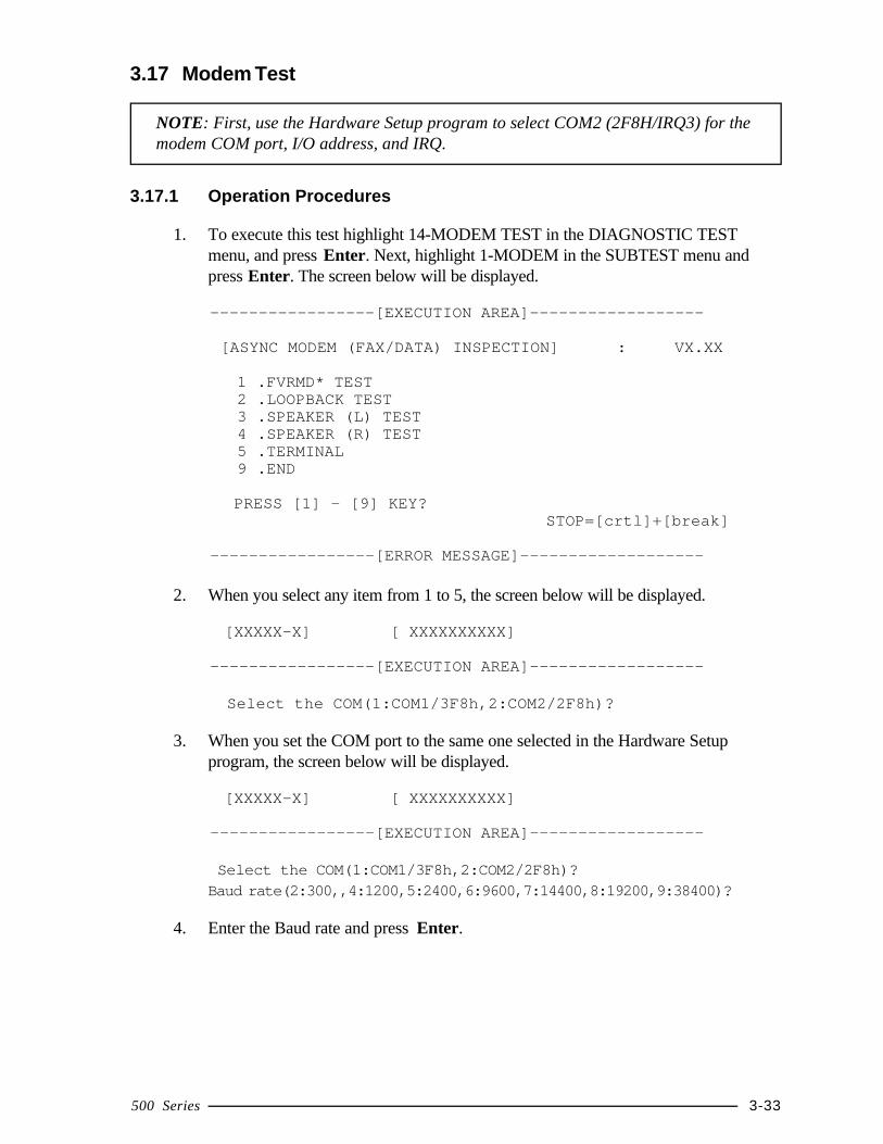
500 Series 3-33
3.17 Modem Test
NOTE: First, use the Hardware Setup program to select COM2 (2F8H/IRQ3) for themodem COM port, I/O address, and IRQ.
3.17.1 Operation Procedures
1. To execute this test highlight 14-MODEM TEST in the DIAGNOSTIC TESTmenu, and press Enter. Next, highlight 1-MODEM in the SUBTEST menu andpress Enter. The screen below will be displayed.
—————————————————[EXECUTION AREA]——————————————————
[ASYNC MODEM (FAX/DATA) INSPECTION] : VX.XX
1 .FVRMD* TEST2 .LOOPBACK TEST3 .SPEAKER (L) TEST4 .SPEAKER (R) TEST5 .TERMINAL9 .END
PRESS [1] - [9] KEY?STOP=[crtl]+[break]
—————————————————[ERROR MESSAGE]———————————————————
2. When you select any item from 1 to 5, the screen below will be displayed.
[XXXXX-X] [ XXXXXXXXXX]
—————————————————[EXECUTION AREA]——————————————————
Select the COM(1:COM1/3F8h,2:COM2/2F8h)?
3. When you set the COM port to the same one selected in the Hardware Setupprogram, the screen below will be displayed.
[XXXXX-X] [ XXXXXXXXXX]
—————————————————[EXECUTION AREA]——————————————————
Select the COM(1:COM1/3F8h,2:COM2/2F8h)?Baud rate(2:300,,4:1200,5:2400,6:9600,7:14400,8:19200,9:38400)?
4. Enter the Baud rate and press Enter.
3-34 500 Series
3.17.2 Program Explanation
Subtest 01 FVRMD*TEST
Initializes the modem and sends an ATZ command.
Subtest 02 LOOPBACK TEST
A loopback signal is sent from board FVRMD* to FLXDA.
Subtest 03 SPEAKER (L) TEST
A dial-tone sound is generated in the left speaker.
Subtest 04 SPEAKER (R) TEST
A dial-tone sound is generated in the right speaker.
Subtest 05 TERMINAL
NOTE: Before you conduct test 05, connect the DAA module to a tele-phone.
When you have connected the DAA module to a telephone, test the connectionby calling the line from another phone.
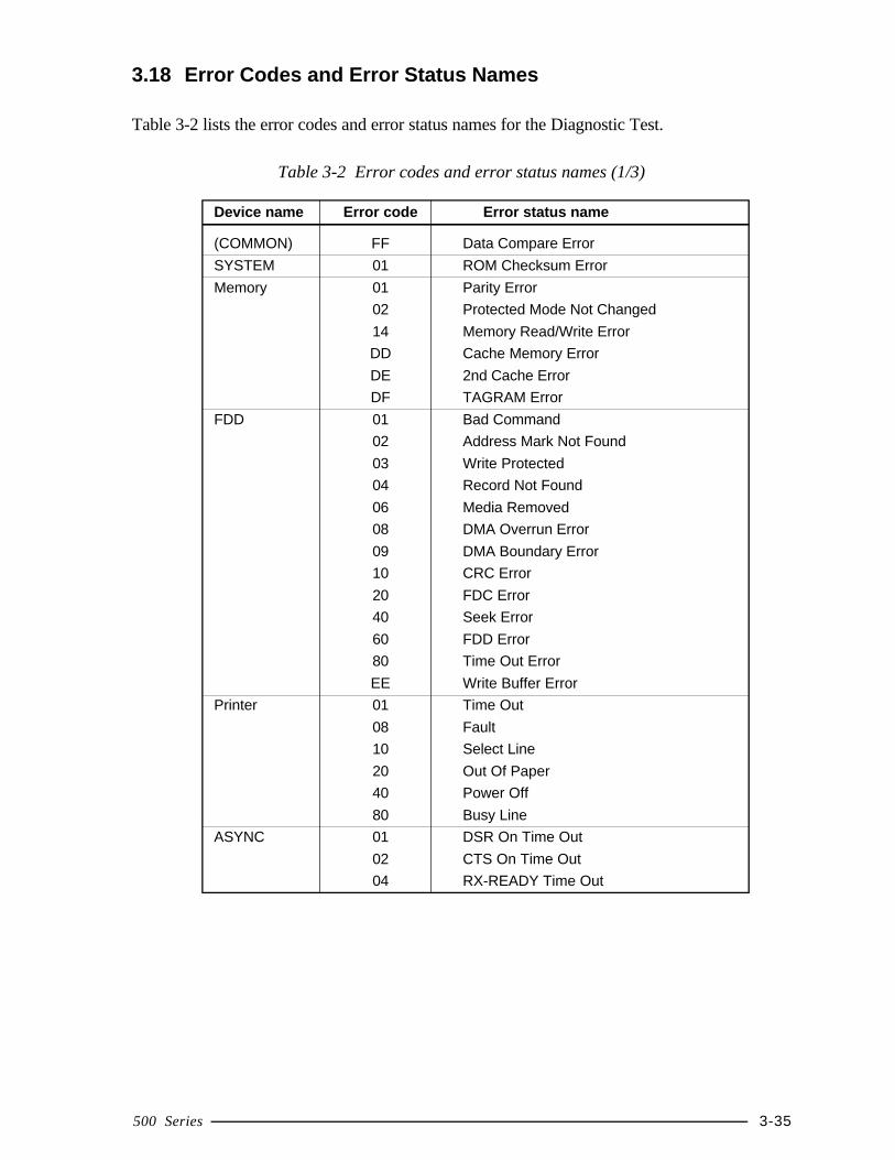
500 Series 3-35
3.18 Error Codes and Error Status Names
Table 3-2 lists the error codes and error status names for the Diagnostic Test.
Table 3-2 Error codes and error status names (1/3)
Device name Error code Error status name
(COMMON) FF Data Compare Error
SYSTEM 01 ROM Checksum Error
Memory 01 Parity Error
02 Protected Mode Not Changed
14 Memory Read/Write Error
DD Cache Memory Error
DE 2nd Cache Error
DF TAGRAM Error
FDD 01 Bad Command
02 Address Mark Not Found
03 Write Protected
04 Record Not Found
06 Media Removed
08 DMA Overrun Error
09 DMA Boundary Error
10 CRC Error
20 FDC Error
40 Seek Error
60 FDD Error
80 Time Out Error
EE Write Buffer Error
Printer 01 Time Out
08 Fault
10 Select Line
20 Out Of Paper
40 Power Off
80 Busy Line
ASYNC 01 DSR On Time Out
02 CTS On Time Out
04 RX-READY Time Out
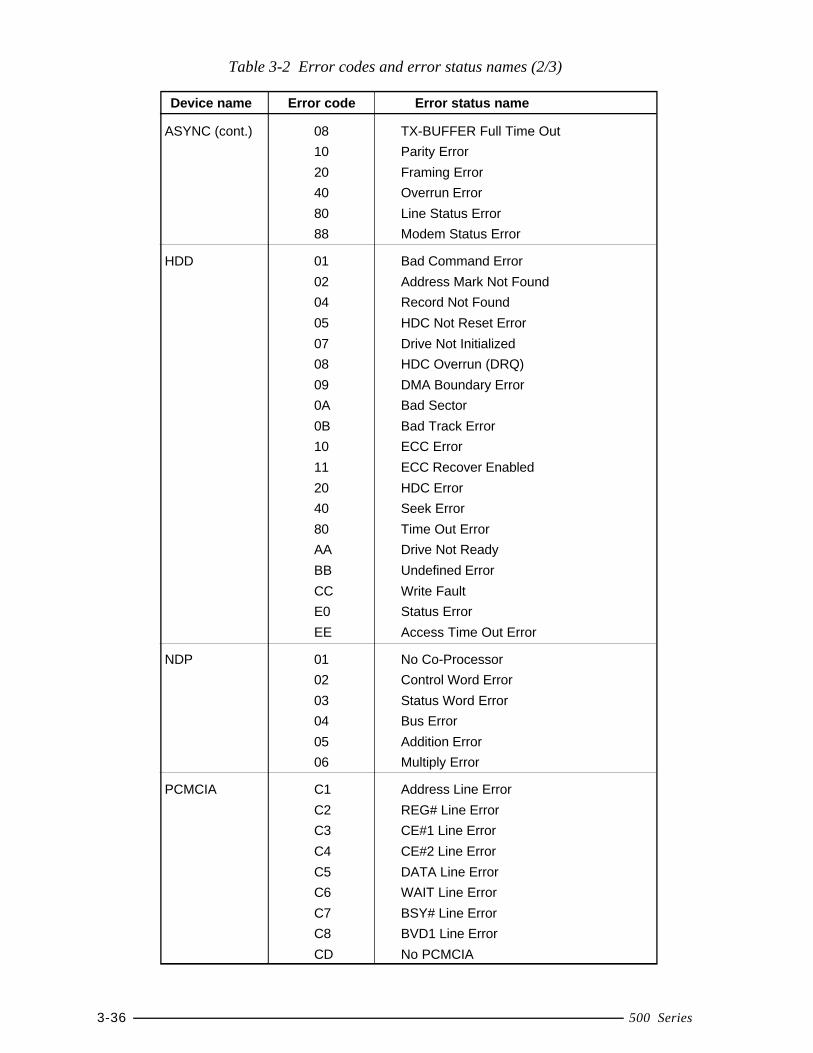
3-36 500 Series
Table 3-2 Error codes and error status names (2/3)
Device name Error code Error status name
ASYNC (cont.) 08 TX-BUFFER Full Time Out
10 Parity Error
20 Framing Error
40 Overrun Error
80 Line Status Error
88 Modem Status Error
HDD 01 Bad Command Error
02 Address Mark Not Found
04 Record Not Found
05 HDC Not Reset Error
07 Drive Not Initialized
08 HDC Overrun (DRQ)
09 DMA Boundary Error
0A Bad Sector
0B Bad Track Error
10 ECC Error
11 ECC Recover Enabled
20 HDC Error
40 Seek Error
80 Time Out Error
AA Drive Not Ready
BB Undefined Error
CC Write Fault
E0 Status Error
EE Access Time Out Error
NDP 01 No Co-Processor
02 Control Word Error
03 Status Word Error
04 Bus Error
05 Addition Error
06 Multiply Error
PCMCIA C1 Address Line Error
C2 REG# Line Error
C3 CE#1 Line Error
C4 CE#2 Line Error
C5 DATA Line Error
C6 WAIT Line Error
C7 BSY# Line Error
C8 BVD1 Line Error
CD No PCMCIA
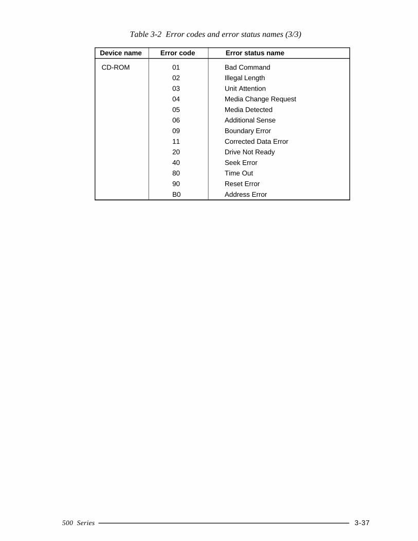
500 Series 3-37
Table 3-2 Error codes and error status names (3/3)
Device name Error code Error status name
CD-ROM 01 Bad Command
02 Illegal Length
03 Unit Attention
04 Media Change Request
05 Media Detected
06 Additional Sense
09 Boundary Error
11 Corrected Data Error
20 Drive Not Ready
40 Seek Error
80 Time Out
90 Reset Error
B0 Address Error
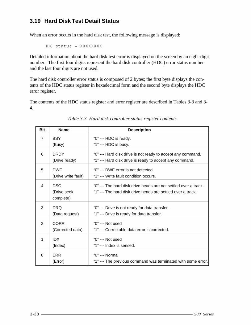
3-38 500 Series
3.19 Hard Disk Test Detail Status
When an error occurs in the hard disk test, the following message is displayed:
HDC status = XXXXXXXX
Detailed information about the hard disk test error is displayed on the screen by an eight-digitnumber. The first four digits represent the hard disk controller (HDC) error status numberand the last four digits are not used.
The hard disk controller error status is composed of 2 bytes; the first byte displays the con-tents of the HDC status register in hexadecimal form and the second byte displays the HDCerror register.
The contents of the HDC status register and error register are described in Tables 3-3 and 3-4.
Table 3-3 Hard disk controller status register contents
Bit Name Description
7 BSY “0” --- HDC is ready.
(Busy) “1” --- HDC is busy.
6 DRDY “0” --- Hard disk drive is not ready to accept any command.
(Drive ready) “1” --- Hard disk drive is ready to accept any command.
5 DWF “0” --- DWF error is not detected.
(Drive write fault) “1” --- Write fault condition occurs.
4 DSC “0” --- The hard disk drive heads are not settled over a track.
(Drive seek “1” --- The hard disk drive heads are settled over a track.
complete)
3 DRQ “0” --- Drive is not ready for data transfer.
(Data request) “1” --- Drive is ready for data transfer.
2 CORR “0” --- Not used
(Corrected data) “1” --- Correctable data error is corrected.
1 IDX “0” --- Not used
(Index) “1” --- Index is sensed.
0 ERR “0” --- Normal
(Error) “1” --- The previous command was terminated with some error.

500 Series 3-39
Table 3-4 Error register contents
Bit Name Description
7 BBK1 “0” Not used
(Bad block “1” A bad block mark is detected.
mark)
6 UNC “0” There is no uncorrectable data error.
(Uncorrectable) “1” Uncorrectable data error has been detected.
5 —— Not used
4 IDNF “0” Not used
(Identification) “1” There was no ID field in the requested sector.
3 —— Not used
2 ABRT “0” Not used
(Abort) “1” Illegal command error or a drive status error occurs.
1 TK00 “0” The hard disk has found track 0 during a recalibrate command.
(Track 0) “1” The hard disk could not find track 0 during a recalibrate command.
0 —— Not used
3-40 500 Series
3.20 Hard Disk Format
This command executes hard disk formatting. There are two types of hard-disk formatting:
❑ Low-level (physical) formatting❑ MS-DOS (logical) formatting
This hard disk format function performs a low-level format of the hard disk and executes thefollowing hard disk formats and check:
1. All track FORMAT2. Good track FORMAT3. Bad track FORMAT4. Bad track CHECK
NOTE: The contents of the hard disk will be erased when this program is executed.Before executing the function, transfer the contents of the hard disk to abackup system (i.e., floppy disks).1. If MS-DOS 6.22/Windows for Workgroups is selected, use the Master
Diskette Creator (MDC) utility in the Toshiba Utility folder to back upthe preinstalled software. After backing up the preinstalled software, usethe BACKUP command in the Toshiba Companion Utility to back up theentire disk, including the user’s files.
2. If Windows 95 is selected, check to see if the Microsoft Create SystemDisks Tools (MSCSD.EXE) still exists in the System Tools Folder. (Thistool can be used only once.) If it exists, use it to back up the preinstalledsoftware, then use the Backup utility in the System Tools folder to backup the entire disk, including the user’s files.
Refer to the appropriate instructions for each operating system.
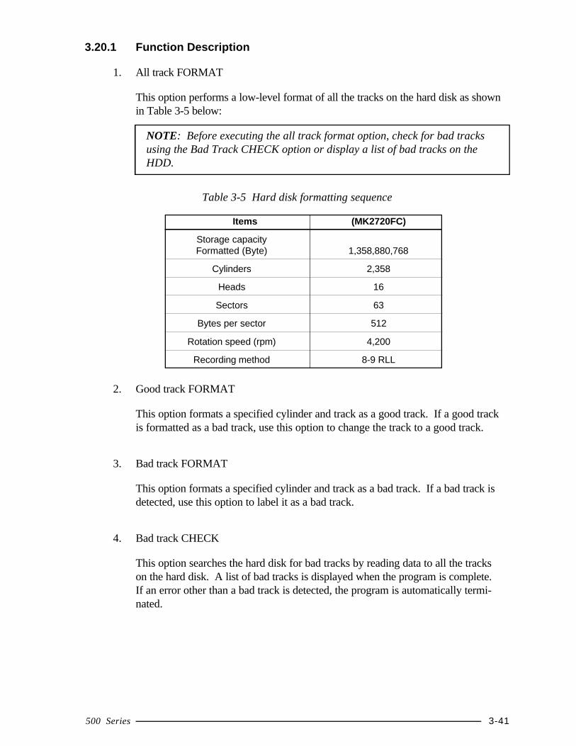
500 Series 3-41
3.20.1 Function Description
1. All track FORMAT
This option performs a low-level format of all the tracks on the hard disk as shownin Table 3-5 below:
NOTE: Before executing the all track format option, check for bad tracksusing the Bad Track CHECK option or display a list of bad tracks on theHDD.
Table 3-5 Hard disk formatting sequence
Items (MK2720FC)
Storage capacityFormatted (Byte) 1,358,880,768
Cylinders 2,358
Heads 16
Sectors 63
Bytes per sector 512
Rotation speed (rpm) 4,200
Recording method 8-9 RLL
2. Good track FORMAT
This option formats a specified cylinder and track as a good track. If a good trackis formatted as a bad track, use this option to change the track to a good track.
3. Bad track FORMAT
This option formats a specified cylinder and track as a bad track. If a bad track isdetected, use this option to label it as a bad track.
4. Bad track CHECK
This option searches the hard disk for bad tracks by reading data to all the trackson the hard disk. A list of bad tracks is displayed when the program is complete.If an error other than a bad track is detected, the program is automatically termi-nated.
3-42 500 Series
3.20.2 Operations
NOTE: After the HDD has been formatted, execute the Toshiba MS-DOS FDISKcommand to partition the HDD. Next, execute the Toshiba MS-DOS FORMAT com-mand. Refer to the Toshiba MS-DOS manual for more information about using thesecommands.
Selecting 2 and pressing Enter on the DIAGNOSTIC MENU displays the following mes-sages:
DIAGNOSTICS - HARD DISK FORMAT : VX.XX
1 - All track FORMAT2 - Good track FORMAT3 - Bad track FORMAT4 - Bad track CHECK9 - Go to TEST MENU
↑↓→← : Select items, Enter: Finish, Esc: Exit
1. All track FORMAT
Pressing 1 selects All track FORMAT, which lets you format the entire disk.
[All track FORMAT]
Drive : #1 = HDD #2 = NonCylinder : XXXXHead : XXSector : XX
<<< Model name = >>>
The following selections also appear at the bottom of the screen insuccession:
Drive number select (1:#1,2:#2) ?
Select a drive number and press Enter. The following message will appear:
Interleave number (1/1 ~ 8) ?
Select an interleave number, 1 ~ 8 and press Enter. Pressing only Enter selects 1.
500 Series 3-43
(a) Bad track register
The Bad Track register prompt will appear as shown below. Enter thecylinder and head numbers of bad tracks and press Enter. Note that if thereare no bad tracks, pressing Enter alone is the same as executing All TrackFormat described in item (c) below.
[ WARNING : Current DISK data will becompletely destroyed ]
Press Bad cylinder number (dddd)] key ? Press Bad head number (dd)] key ?
Enter the cylinder and head number in the format above in decimal notation.Repeat for each bad track you want to format.
After entering the bad tracks, press Enter to execute the format.
(b) All track format
All tracks are formatted as good tracks except those registered as bad tracksin item (a) above or those identified as bad tracks in track verification de-scribed in item (c) below.
(c) Track verification
A check is made of all tracks and if an ECC error, ECC-correctable-dataerror, or record-not-found error is detected at a track, that track is automati-cally formatted as a bad track.
2. Good track FORMAT
If a good track has been erroneously formatted as a bad track, you can use thissubtest to reformat the track as a good track. To format a track as a good track,enter the number for drive, interleave, cylinder, and head as indicated in the screenprompt shown below.
Drive number select (1:#1, 2:#2) ? Interleave number (1 / 1 - 8) ?
Press [Cylinder number (dddd)] ?Press [Head number (dd)] ?
Press Enter to return to the Hard Disk Format menu.
3-44 500 Series
3. Bad track FORMAT
To format a track as a bad track, enter the number for drive, interleave, cylinder,and head as indicated in the screen prompt shown below.
Drive number select (1:#1, 2:#2) ?Interleave number (1 / 1 - 8) ?
Press [Cylinder number (dddd)] ?Press [Head number (dd)] ?
Press Enter to return to the Hard Disk Format menu.
4. Bad track CHECK
This subtest reads the entire disk and displays a list of bad tracks. The test isterminated in case of a bad track check error. To initiate the subtest enter thedrive number at the prompt shown below.
Drive number select (1:#1, 2:#2) ?
Bad tracks will be displayed in the format shown below.
[[cylinder, head = 0123 03]]
Press Enter to return to the Hard Disk Format menu.
500 Series 3-45
3.21 Head Cleaning
3.21.1 Function Description
This function cleans the heads in the FDD by executing a series of head load/seek and readoperations. A cleaning kit is necessary to perform this program.
3.21.2 Operations
1. Selecting 4 on the DIAGNOSTIC MENU and pressing Enter displays the follow-ing messages:
DIAGNOSTICS - FLOPPY DISK HEAD CLEANING : VX.XX
Mount cleaning disk(s) on drive(s).
Press any key when ready.
2. Remove the Diagnostics Disk from the FDD. Insert the cleaning disk and pressEnter.
3. When the "cleaning start" message appears, the FDD head cleaning has begun.
4. The display automatically returns to the DIAGNOSTIC MENU when the programis completed.
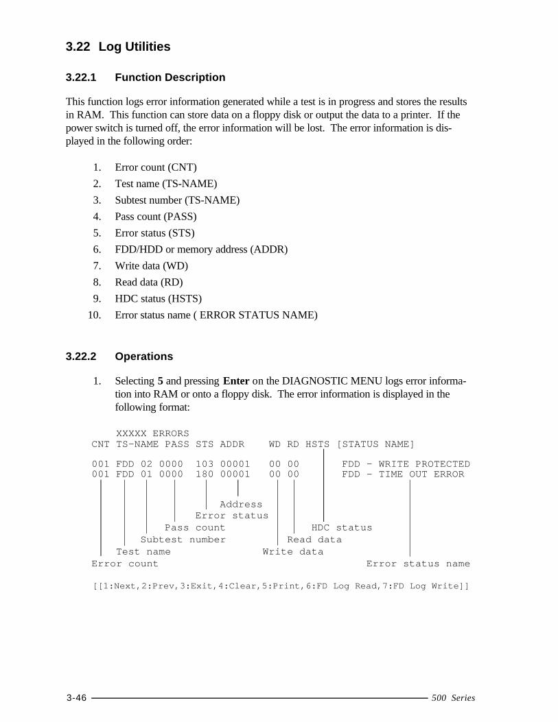
3-46 500 Series
3.22 Log Utilities
3.22.1 Function Description
This function logs error information generated while a test is in progress and stores the resultsin RAM. This function can store data on a floppy disk or output the data to a printer. If thepower switch is turned off, the error information will be lost. The error information is dis-played in the following order:
1. Error count (CNT)2. Test name (TS-NAME)3. Subtest number (TS-NAME)4. Pass count (PASS)5. Error status (STS)6. FDD/HDD or memory address (ADDR)7. Write data (WD)8. Read data (RD)9. HDC status (HSTS)
10. Error status name ( ERROR STATUS NAME)
3.22.2 Operations
1. Selecting 5 and pressing Enter on the DIAGNOSTIC MENU logs error informa-tion into RAM or onto a floppy disk. The error information is displayed in thefollowing format:
XXXXX ERRORSCNT TS-NAME PASS STS ADDR WD RD HSTS [STATUS NAME]
001 FDD 02 0000 103 00001 00 00 FDD - WRITE PROTECTED001 FDD 01 0000 180 00001 00 00 FDD - TIME OUT ERROR
Address Error status Pass count HDC status Subtest number Read data Test name Write dataError count Error status name
[[1:Next,2:Prev,3:Exit,4:Clear,5:Print,6:FD Log Read,7:FD Log Write]]
500 Series 3-47
2. The error information displayed on the screen can be manipulated by the followingnumber keys:
The 1 key scrolls the display to the next page.The 2 key scrolls the display to the previous page.The 3 key returns to the Diagnostic Menu.The 4 key erases all error log information in RAM.The 5 key outputs the error log information to a printer.The 6 key reads the log information from a floppy disk.The 7 key writes the log information to a floppy disk.
3. In the case of “error retry OK,” a capital “R” will be placed at the beginning of theerror status. However, it is not added to the error count.
3-48 500 Series
3.23 Running Test
3.23.1 Function Description
This function automatically executes the following tests in sequence:
1. System test (subtest number 01)2. Memory test (subtest number 01, 02, 04, 06)3. Display test (subtest number 01 to 06)4. FDD test (subtest number 02)5. HDD test (subtest number 01, 05)6. Real timer test (subtest number 02)7. Printer test (subtest number 03), if selected8. Async test (subtest number 01), if selected
The system automatically detects the number of floppy disk drives connected to the computerfor the FDD test.
3.23.2 Operations
NOTE: Do not forget to load a work disk in the FDD. If a work disk is not loaded, anerror will be generated during the FDD testing.
1. Remove the diagnostics disk from the floppy disk drive and insert the work disk.
2. Selecting 6 on the Diagnostic Menu and pressing Enter displays the followingmessage:
Printer wrap around test (Y/N) ?
Selecting Y (yes) executes the printer wraparound test. A printer wraparoundconnector must be connected to the parallel port of the computer to properlyexecute this test.
3. Selecting Y or N and pressing Enter displays the following message:
Serial #A wrap around test (Y/N) ?
Selecting Y (yes) executes the ASYNC wraparound test. An RS-232-C wrap-around connector must be connected to the serial port of the computer to properlyexecute this test.
500 Series 3-49
4. Select Yes or No and press Enter. The following message will appear:
Mount the work disk(s) on the drive(s),then press [Enter] key.[Warning : The contents of the disk(s),will be destroyed.]
5. This program is executed continuously. To terminate the program, press Ctrl +Break.
3-50 500 Series
3.24 Floppy Disk Drive Utilities
3.24.1 Function Description
This function formats the FDD, copies the floppy disk, and displays the dump list for both theFDD and HDD.
1. FORMAT
NOTE: This program is only for testing a floppy disk drive. The option isdifferent from the Toshiba MS-DOS FORMAT command.
This program can format a 5.25-inch or 3.5-inch floppy disk in the followingformats:
(a) 2D: Double-sided, double-density, 48/67.5 TPI, MFM mode, 512 bytes, 9sectors/track.
(b) 2DD: Double-sided, double-density, double-track, 96/135 TPI, MFM mode,512 bytes, 9 sectors/track.
(c) 2HD: Double-sided, high-density, double-track, 96/135 TPI, MFM mode,512 bytes, 18 sectors/track.
2. COPY
This program copies data from a source floppy disk to a target floppy disk.
3. DUMP
This program displays the contents of the floppy disk and the designated sectors ofthe hard disk on the display.
3.24.2 Operations
1. Selecting 7 on the DIAGNOSTIC MENU and pressing Enter displays the follow-ing message:
[ FDD UTILITIES ]
1 - FORMAT2 - COPY3 - DUMP9 - EXIT TO DIAGNOSTICS MENU
500 Series 3-51
2. FORMAT program
(a) Selecting FORMAT displays the following message:
DIAGNOSTICS - FLOPPY DISK FORMAT : VX.XX
Drive number select (1:A, 2:B) ?
(b) Select a drive number to display the following message:
Type select (0:2DD-2DD,1:2D-2D,2:2D-2HD,3:2HD-2HD) ?
(c) Select a media/drive type number and press Enter. A message similar to theone below will be displayed:
Warning : Disk data will be destroyed.
Insert work disk into drive A: Press any key when ready.
(d) Remove the Diagnostics Disk from the FDD, insert the work disk, and pressany key.
The following message will be displayed when the FDD format is executed: [ FDD TYPE ] : TRACK = XXX [ FDD TYPE ] : HEAD = X [ FDD TYPE ] : SECTOR = XX
Format start[[track, head = XXX X]]
After the floppy disk is formatted, the following message will appear:
Format complete Another format (1:Yes/2:No) ?
(e) Typing 1 displays the message from step (c) above. Typing 2 returns the testto the DIAGNOSTIC MENU.
3. COPY program
(a) When COPY is selected, the following message appears:
FLOPPY DISK FORMAT & COPY : VX.XX Type select (0:2DD-2DD,1:2D-2D,2:2D-2HD,3:2HD-2HD) ?
(b) Selecting a media/drive type number will display a message similar to the onebelow: Insert source disk into drive A: Press any key when ready.
(c) Remove the Diagnostics Disk from the FDD, insert the source disk, andpress any key. The following message will appear, indicating the programhas started.
3-52 500 Series
[ FDD TYPE ] : TRACK = XXX [ FDD TYPE ] : HEAD = X [ FDD TYPE ] : SECTOR = XX
Copy start[[ track,head = XXX X ]]
(d) Remove the source disk from the FDD, insert a formatted work disk, andpress any key. The [[ track, head = XXX X ]] message will appear andstart copying to the target disk. When the amount of data is too large to becopied in one operation, the message from step (b) is displayed again. Afterthe floppy disk has been copied, the following message will appear: Copy complete Another copy (1:Yes/2:No) ?
(e) To copy another disk, type 1 and the message from step (a) will be displayedagain. Entering 2 returns the test program to the DIAGNOSTIC MENU.
4. DUMP program
(a) When dump is selected, the following message appears:
DIAGNOSTICS-HARD DISK & FLOPPY DISK DUMP : VX.XX Drive type select (1:FDD, 2:HDD) ?
(b) Select a drive type. If 1 is selected in step (a), the following message dis-plays.
Select drive number (1:A, 2:B) ?
If 2 is selected, the following message displays:
Select drive number (1:C, 2:D) ?
After selecting the HDD, the display will go to step (f).
(c) The following message will be displayed:
Format type select (1:2DD, 2:2D, 3:2HD) ?
(d) Select a format type. The following message will appear:
Insert source disk into drive A: Press any key when ready.
(e) Insert a source disk, press any key, and the following message will appear:
—— Max. address —— [Track ] = 0079 [ Head ] = 01 [Sector] = 09
Track number ??
Set the track number you want to dump. The system will access the disk anddump a list.
500 Series 3-53
3.25 System Configuration
3.25.1 Function Description
The System Configuration program contains the following configuration information for thecomputer:
1. BIOS ROM version2. Boot ROM version3. KBC version4. PS Microprocessor Version5. Base memory size6. The number of floppy disk drives7. The number of ASYNC ports8. The number of hard disk drives9. The number of printer ports
10. Extended Memory Size11. The number of math co-processors
3.25.2 Operations
Selecting 8 on the DIAGNOSTIC MENU and pressing Enter displays the following systemconfiguration:
SYSTEM CONFIGURATION :
* - BIOS ROM VERSION = VX.XX* - BOOT ROM VERSION = VX.XX* - KBC VERSION = VX.XX* - PS MICOM VERSION = VX.XX* - 639KB MEMORY* - 1 FLOPPY DISK DRIVE(S)* - 1 ASYNC ADAPTER* - 1 HARD DISK DRIVE(S)* - 1 PRINTER ADAPTER* - XXXMB + XXXXKB EXTENDED MEMORY* - 1 MATH CO-PROCESSOR
Press [Enter] Key
Press Enter to return to the DIAGNOSTIC MENU.
3-54 500 Series
3.26 SETUP
3.26.1 Function Description
This program displays the current system setup information as listed below:
1. Memory(a) Total
2. Display(a) Display Adapter(b) LCD Display Colors(c) Power On Display(d) Text Mode Stretch
3. Password(a) User Password(b) Eject Password
4. Hard Disk
5. Battery
6. Others(a) Power-up Mode(b) CPU Cache(c) Level 2 Cache(d) Auto Power On(e) Alarm Volume(f) System Beep(g) Panel Power On/Off(h) Keyboard(i) Boot Priority(j) Pointing Devices(k) PC Card Controller Mode
7. Display
8. I/O Ports(a) Serial Port(b) Infrared Port(c) Built-in Modem Port(d) Parallel Port(e) Sound System
9. PCI Bus
10. Drives I/O
11. Floppy Disk I/O
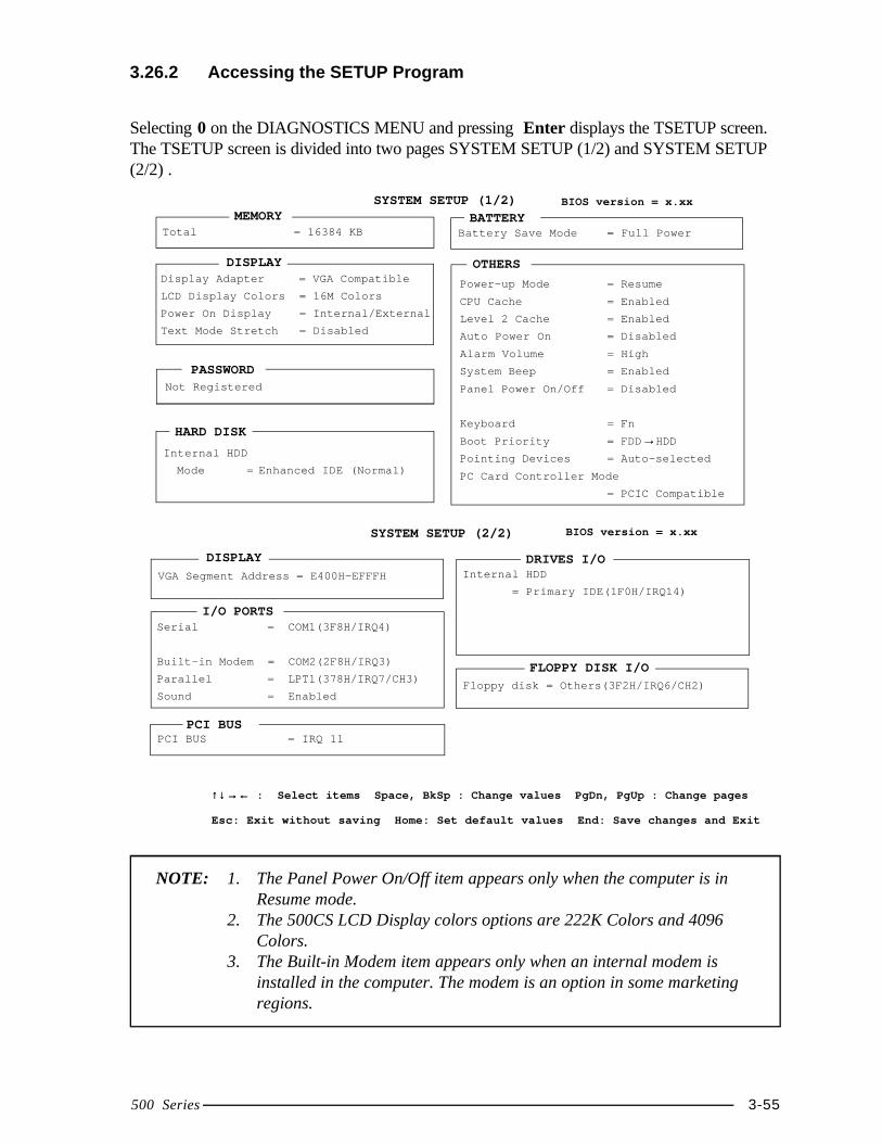
500 Series 3-55
3.26.2 Accessing the SETUP Program
Selecting 0 on the DIAGNOSTICS MENU and pressing Enter displays the TSETUP screen.The TSETUP screen is divided into two pages SYSTEM SETUP (1/2) and SYSTEM SETUP(2/2) .
↑↓→←↑↓→← : Select items Space, BkSp : Change values PgDn, PgUp : Change pages
Esc: Exit without saving Home: Set default values End: Save changes and Exit
NOTE: 1. The Panel Power On/Off item appears only when the computer is inResume mode.
2. The 500CS LCD Display colors options are 222K Colors and 4096Colors.
3. The Built-in Modem item appears only when an internal modem isinstalled in the computer. The modem is an option in some marketingregions.
MEMORYBIOS version = x.xxSYSTEM SETUP (1/2)
Total = 16384 KB
DISPLAYDisplay Adapter = VGA Compatible
LCD Display Colors = 16M Colors
Power On Display = Internal/External
Text Mode Stretch = Disabled
HARD DISK Battery Save Mode = Full Power
BATTERY
Serial = COM1(3F8H/IRQ4)
Built-in Modem = COM2(2F8H/IRQ3)
Parallel = LPT1(378H/IRQ7/CH3)
Sound = Enabled
PCI BUS = IRQ 11
SYSTEM SETUP (2/2) BIOS version = x.xx
Internal HDD
= Primary IDE(1F0H/IRQ14)
DRIVES I/O
I/O PORTS
DISPLAY
PCI BUS
VGA Segment Address = E400H-EFFFH
Floppy disk = Others(3F2H/IRQ6/CH2)
FLOPPY DISK I/O
OTHERS
Power-up Mode = Resume
CPU Cache = Enabled
Level 2 Cache = Enabled
Auto Power On = Disabled
Alarm Volume = High
System Beep = Enabled
Panel Power On/Off = Disabled
Keyboard = Fn
Boot Priority = FDD→HDD
Pointing Devices = Auto-selected
PC Card Controller Mode
= PCIC Compatible
HARD DISKHARD DISK
Internal HDD
Mode = Enhanced IDE (Normal)
Not Registered
PASSWORD
3-56 500 Series
3.26.3 Moving Within the SETUP Menu and Changing Values
1. Press ← and → to move between the two columns. Press ↑ and ↓ to move be-tween items in a column.
2. Press either the spacebar or BkSp to change the value.
NOTE: 1. On either page, you can go directly to a specific group bypressing the first letter (highlighted) of the group’s name. Forexample, B to go to the Battery group.
2. To change pages, press the PgUp (page up) or PgDn (pagedown) key.
3.26.4 Accepting Changes and Exiting the SETUP Window
1. Press End to accept the changes you made.
If the changed item does not require the system to reboot, the following message isdisplayed:
Are you sure? (Y/N)
If the changed item requires the system to reboot, the following message is dis-played:
Are you sure? (Y/N)The changes you made will cause the system to reboot.
(a) To make other changes, press N. Repeat the steps above.
(b) To accept the changes, press Y.
NOTE: You can press Esc to quit at any time without saving changes.SETUP asks you to confirm that you don’t want to save your changes.
3.26.5 The Factory Preset Configuration
When you access SETUP, the current configuration is displayed.
1. To show the factory preset configuration, press Home.
2. To accept the default settings, press End and then press Y.
NOTE: When you execute the default setting, the following settings are notchanged:
HDD Mode Password Sound System Write Policy
500 Series 3-57
3.26.6 SETUP Options
The SETUP screen is divided into functionally related groups. This section describes eachgroup and its options.
1. Memory
This option lists the computer’s memory allocation.
(a) Total
Displays the total amount of memory installed and is automatically calculatedby the computer. You cannot change this value.
2. Display
This option configures the computer’s display.
(a) Display Adapter
Enables or disables the internal controller for the VGA internal display.
VGA compatible Enables the internal VGA controller. (Default)
Not Used Disables the internal VGA controller.
(b) LCD Display Colors
Selects the color palette of the internal TFT display when the LCD mode isset to Color.
222K colors Displays 64k colors out of 226,981 colors, or(500CS) 4096 which displays 4096 colors out of 4096 colors.
16M colors Displays up to 16,777,216 colors simultaneously.(500CDT) (This value cannot be changed.)
(c) Power On Display
Selects the display when booting up the computer.
Internal/External Selects an external CRT if one is connected, other-wise it selects the internal LCD. (Default)
Simultaneous Selects both the internal LCD and the external CRTfor simultaneous display.
3-58 500 Series
NOTE: When starting the computer in Resume mode, the last configuration isremembered. If data does not appear on the display you are using afterstarting in Resume mode, press Fn+F5.Pressing Fn+F5 changes the display setting as follows: internal LCD tosimultaneous to external CRT.
(d) Text Mode Stretch
Text mode stretch enables a larger display area of the screen.
Enabled Enables the text mode stretch feature.
Disabled Disables the text mode stretch feature. (Default)
3. Password
(a) User Password
Sets or resets the user password for power on and instant security.
Registered The user password has been registered.
Not registered The user password has not been registered.
(b) Eject Password
Prevents an unauthorized user from removing the computer from an optionalDesk Station V Plus.
Enabled The eject password has been registered.
Disabled The eject password has not been registered.
For details on setting the user and eject password refer to your 500 SeriesUser’s Guide.
4. Hard Disk
Selects the internal hard disk mode.
Enhanced IDE Select this mode when using MS-DOS ®, (Normal)Windows® for Workgroups, Windows 95, orOS/2®. (Default)
Standard IDE Select this mode when using Novell ® NetWare® orUNIX®. When this mode is selected, up to 504MBis logically available even though the disk’s capacityis larger than 504MB.
No drive An HDD is not installed.
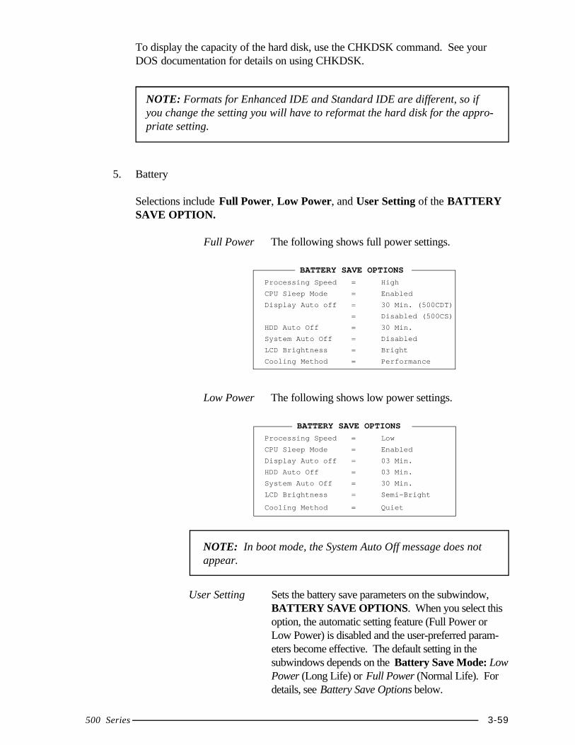
500 Series 3-59
To display the capacity of the hard disk, use the CHKDSK command. See yourDOS documentation for details on using CHKDSK.
NOTE: Formats for Enhanced IDE and Standard IDE are different, so ifyou change the setting you will have to reformat the hard disk for the appro-priate setting.
5. Battery
Selections include Full Power, Low Power, and User Setting of the BATTERYSAVE OPTION.
Full Power The following shows full power settings.
BATTERY SAVE OPTIONS
Processing Speed = High
CPU Sleep Mode = Enabled
Display Auto off = 30 Min. (500CDT)
= Disabled (500CS)
HDD Auto Off = 30 Min.
System Auto Off = Disabled
LCD Brightness = Bright
Cooling Method = Performance
Low Power The following shows low power settings.
BATTERY SAVE OPTIONS
Processing Speed = Low
CPU Sleep Mode = Enabled
Display Auto off = 03 Min.
HDD Auto Off = 03 Min.
System Auto Off = 30 Min.
LCD Brightness = Semi-Bright
Cooling Method = Quiet
NOTE: In boot mode, the System Auto Off message does notappear.
User Setting Sets the battery save parameters on the subwindow,BATTERY SAVE OPTIONS. When you select thisoption, the automatic setting feature (Full Power orLow Power) is disabled and the user-preferred param-eters become effective. The default setting in thesubwindows depends on the Battery Save Mode: LowPower (Long Life) or Full Power (Normal Life). Fordetails, see Battery Save Options below.

3-60 500 Series
(a) Battery Save Options
The following set of options can be selected in the submenu of User Setting(one of the Battery Save Mode options).
(1) Processing Speed
This feature changes the CPU processing speed.
High CPU operates at high speed. (Default)
Low CPU operates at low speed.
(2) CPU Sleep Mode
Use this option to enable or disable the CPU sleep function.
Enabled Enables sleep mode.
Disabled Disables sleep mode.
(3) Display Auto Off
Use this option to disable or set the duration of the display automaticpower off function. This function causes the computer to turn the LCDpanel illumination off if you make no entry for the set period of time.
Disabled Disables display automatic power off.
xx Min. Automatically turns off power to the LCD panelillumination if the panel is not used for the durationset. The duration xx can be set to 1, 3, 5, 10, 15,20, or 30 minutes.
(4) HDD Auto Off
Use this option to set the duration of the HDD automatic power offfunction.
Disabled Disables the HDD automatic power off.
xx Min. Automatically turns off power to the hard disk driveif it is not used for the duration set. The duration xxcan be set to 1, 3, 5, 10, 15, 20, 30, or 45 minutes.
(5) System Auto Off
Use this option to enable or disable the system automatic off function inResume mode when you are working in DOS. In Boot mode, it isdisabled and not displayed.
500 Series 3-61
Disabled Disables system automatic power off.
xx Min. Automatically turns off power to the system if it isnot used for the duration set. The duration xx canbe set to 10, 20, 30, 40, 50, or 60 minutes.
(6) LCD Brightness
Use this option to set the level of LCD brightness.
Bright Full brightness for maximum visibility.
Semi-Bright Less than full brightness for saving power.
(7) Cooling method
Performance If the CPU becomes too hot, the fan turns onautomatically. When the CPU temperature falls to anormal range, high-speed processing is resumed andthe fan turns off.
Quiet If the CPU becomes too hot, the processing speed islowered. If the temperature is still too high, the fanturns on. When the CPU temperature falls to a normalrange, the fan turns off and the processing speed isincreased.
6. Others
Whether or not you need to configure the computer with these options dependsprimarily on the kind of software or peripherals you use.
(a) Power-up Modes
Lets you choose between AutoResume and boot mode. You can also set thisoption using hotkeys. AutoResume is effective with either the internal LCDor with an external monitor.
Boot Turns on boot mode. (Default)
Resume Turns on the AutoResume feature.
(b) CPU Cache
Use this feature to enable or disable the CPU cache.
Enabled Enables the CPU cache. (Default)
Disabled Disables the CPU cache.
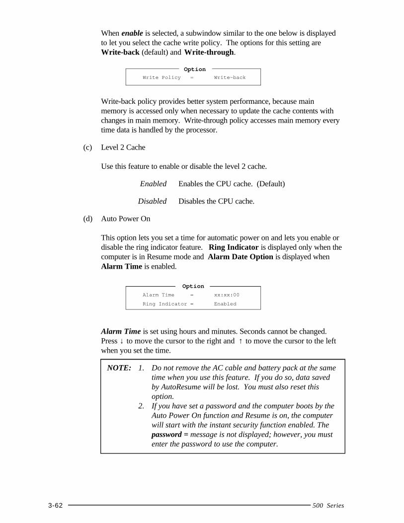
3-62 500 Series
When enable is selected, a subwindow similar to the one below is displayedto let you select the cache write policy. The options for this setting areWrite-back (default) and Write-through.
OptionWrite Policy = Write-back
Write-back policy provides better system performance, because mainmemory is accessed only when necessary to update the cache contents withchanges in main memory. Write-through policy accesses main memory everytime data is handled by the processor.
(c) Level 2 Cache
Use this feature to enable or disable the level 2 cache.
Enabled Enables the CPU cache. (Default)
Disabled Disables the CPU cache.
(d) Auto Power On
This option lets you set a time for automatic power on and lets you enable ordisable the ring indicator feature. Ring Indicator is displayed only when thecomputer is in Resume mode and Alarm Date Option is displayed whenAlarm Time is enabled.
OptionAlarm Time = xx:xx:00
Ring Indicator = Enabled
Alarm Time is set using hours and minutes. Seconds cannot be changed.Press ↓ to move the cursor to the right and ↑ to move the cursor to the leftwhen you set the time.
NOTE: 1. Do not remove the AC cable and battery pack at the sametime when you use this feature. If you do so, data savedby AutoResume will be lost. You must also reset thisoption.
2. If you have set a password and the computer boots by theAuto Power On function and Resume is on, the computerwill start with the instant security function enabled. Thepassword = message is not displayed; however, you mustenter the password to use the computer.
500 Series 3-63
(e) Alarm Volume
This option disables or sets the volume level of the alarm. Setting this optionto off disables the computer’s sound function for alarms. This option canalso be set with hotkeys.
Off Disables the alarm.Low Sets the alarm volume to low.
Medium Sets the alarm volume to medium.
High Sets the alarm volume to high. (Default)
When Alarm Volume is selected, the subwindow below is displayed to letyou enable or disable certain functions.
ALARM VOLUME OPTIONSLow Battery Alarm = Enabled
Panel Close Alarm = Enabled
Enabled Enables the feature. (Default)Disabled Disables the feature.
(f) System Beep
Use this feature to enable or disable the system beep.
Enabled Enables the feature. (Default)Disabled Disables the feature.
(g) Panel Power On/Off
This option allows you to automatically turn your computer on or off byopening or closing the display panel. If this feature is enabled when thecomputer is in Resume mode, the system is automatically powered off whenthe display panel is closed and powered on when the panel is opened. Thisoption does not appear when the computer is in boot mode.
Enabled Enables the feature.Disabled Disables the feature. (Default)
NOTE: Do not remove the AC cable and battery pack at the same timewhen you use this feature. If you do so, data saved by AutoResume willbe lost. You must also reset this option.
3-64 500 Series
(h) Keyboard
This option lets you change the keyboard layout and set the Fn key equiva-lent when you are using an external keyboard. Selecting this option displaysthe following subwindow.
KEYBOARD
Ext. Keyboard “Fn” key equivalent
= Disabled
(1) Ext. Keyboard Fn key equivalent
Use this option to set a key combination on an external keyboard toemulate the Fn key on the computer’s internal keyboard. Setting anFn key equivalent will enable you to use “Hot keys” by pressing theset combination in place of the Fn key.
Disabled No Fn key equivalent. (Default)
Fn Equivalent Left Ctrl + Left Alt*Right Ctrl + Right Alt*Left Alt + Left ShiftRight Alt + Right ShiftLeft Alt + Caps Lock
* If these selections are made, you cannot warm boot the systemby pressing Ctrl + Alt + Del.
(i) Boot Priority
Use this option to select the disk drive priority for boot up.
FDD HDD The computer looks for bootable files first on theFDD and next on the HDD. (Default)
HDD FDD The computer looks for bootable files first on theHDD and next on the FDD.
You can reverse the order by holding down the F10 key while thecomputer is booting. This procedure alternates the setup setting.
500 Series 3-65
(j) Pointing Devices
This option enables or disables the AccuPoint.
Auto selected If the PS/2 mouse is connected to the computerwhen you turn on the power, the PS/2 mouse isenabled and the AccuPoint is disabled. Otherwise,the AccuPoint is enabled. (Default)
Simultaneous Enables both the AccuPoint and the PS/2 mouse.
(k) PC Card Controller Mode
Use this option to set the PC card controller mode.
PCIC Compatible For PCMCIA R2.01 and ZV port card. (Default)
CardBus/16bit For PC card 16 multi-function card, CardBus card,and ZV port card.
7. Display
Use this option to set the VGA segment address from the following options:
(a) VGA Segment Address
E000h-EFFFhE400h-EFFFh (Default)C000h-CBFFhE000h-EBFFh
8. I/O ports
This option controls settings for serial and parallel ports and for the sound system.It also controls the setting for the joystick on the optional Desk Station V Plus.
NOTE: Do not assign the same interrupt request level and I/O address to theserial port and PC card.
3-66 500 Series
(a) Serial Port
This option allows you to set the COM level for the serial port. The serialport interrupt request level (IRQ) and I/O port base address for each COMlevel is shown below:
COM level Interrupt level I/O address
COM1 4 3F8H (Serial port default)
COM2 3 2F8H
COM3 4 3E8H
COM3 5 3E8H
COM3 7 3E8H
COM4 3 2E8H
COM4 5 2E8H
COM4 7 2E8H
Not used (Disables port)
Others (Made automatically by plug-and-playoperating systems)
NOTE: If the setting for the serial port is the same as that for theinfrared or Modem port, the infrared or Modem port is automaticallyset to disabled.
(b) Infrared Port
This option allows you to set the COM level for the infrared port. Theinfrared port interrupt request level (IRQ) and I/O port base address for eachCOM level is shown below.
COM level Interrupt level I/O address
COM1 4 3F8H
COM2 3 2F8H
COM3 4 3E8H
COM3 5 3E8H
COM3 7 3E8H
COM4 3 2E8H
COM4 5 2E8H
COM4 7 2E8H
Not used (Disables port)(Infrared port default)
Others (Made automatically by plug-and-play operating systems)
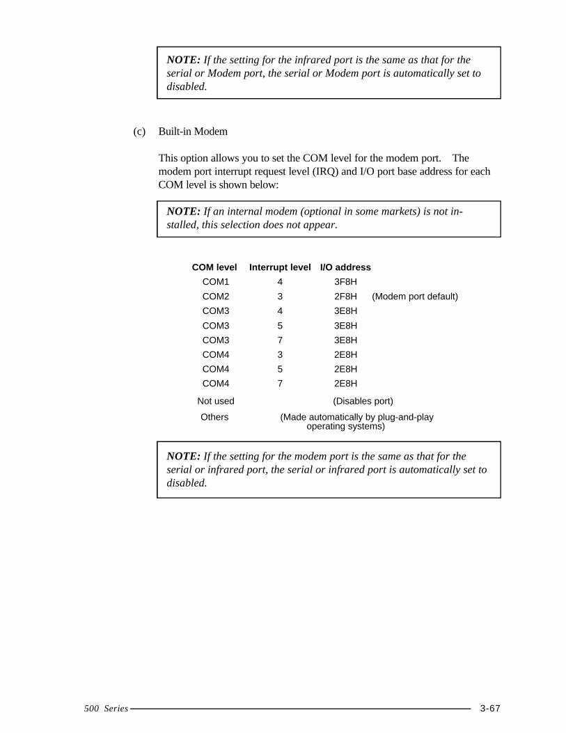
500 Series 3-67
NOTE: If the setting for the infrared port is the same as that for theserial or Modem port, the serial or Modem port is automatically set todisabled.
(c) Built-in Modem
This option allows you to set the COM level for the modem port. Themodem port interrupt request level (IRQ) and I/O port base address for eachCOM level is shown below:
NOTE: If an internal modem (optional in some markets) is not in-stalled, this selection does not appear.
COM level Interrupt level I/O address
COM1 4 3F8H
COM2 3 2F8H (Modem port default)
COM3 4 3E8H
COM3 5 3E8H
COM3 7 3E8H
COM4 3 2E8H
COM4 5 2E8H
COM4 7 2E8H
Not used (Disables port)
Others (Made automatically by plug-and-playoperating systems)
NOTE: If the setting for the modem port is the same as that for theserial or infrared port, the serial or infrared port is automatically set todisabled.
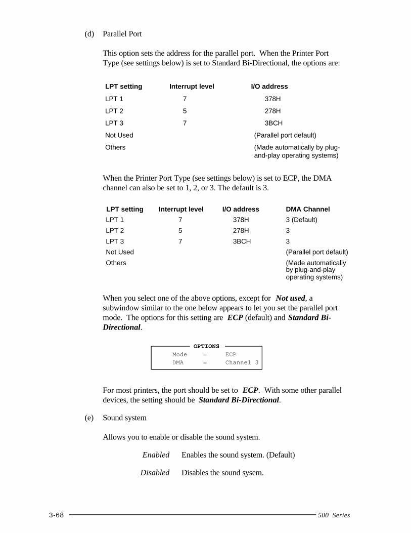
3-68 500 Series
(d) Parallel Port
This option sets the address for the parallel port. When the Printer PortType (see settings below) is set to Standard Bi-Directional, the options are:
LPT setting Interrupt level I/O address
LPT 1 7 378H
LPT 2 5 278H
LPT 3 7 3BCH
Not Used (Parallel port default)
Others (Made automatically by plug-and-play operating systems)
When the Printer Port Type (see settings below) is set to ECP, the DMAchannel can also be set to 1, 2, or 3. The default is 3.
LPT setting Interrupt level I/O address DMA Channel
LPT 1 7 378H 3 (Default)
LPT 2 5 278H 3
LPT 3 7 3BCH 3
Not Used (Parallel port default)
Others (Made automaticallyby plug-and-playoperating systems)
When you select one of the above options, except for Not used, asubwindow similar to the one below appears to let you set the parallel portmode. The options for this setting are ECP (default) and Standard Bi-Directional.
OPTIONS
Mode = ECPDMA = Channel 3
For most printers, the port should be set to ECP. With some other paralleldevices, the setting should be Standard Bi-Directional.
(e) Sound system
Allows you to enable or disable the sound system.
Enabled Enables the sound system. (Default)
Disabled Disables the sound sysem.
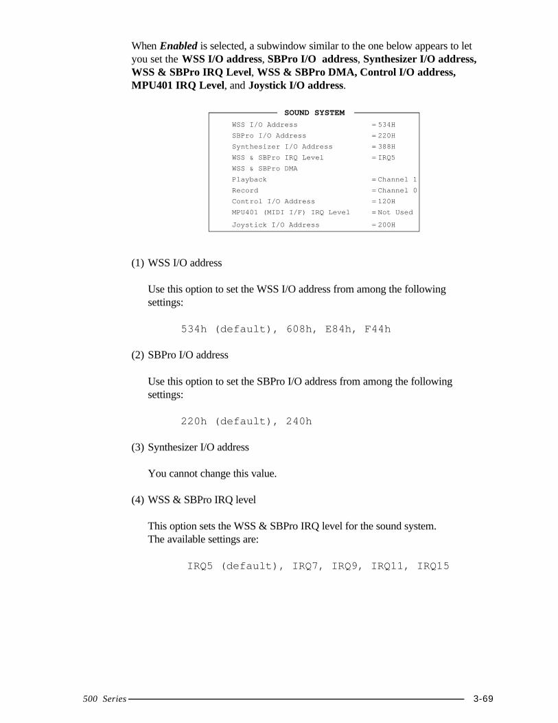
500 Series 3-69
When Enabled is selected, a subwindow similar to the one below appears to letyou set the WSS I/O address, SBPro I/O address, Synthesizer I/O address,WSS & SBPro IRQ Level, WSS & SBPro DMA, Control I/O address,MPU401 IRQ Level, and Joystick I/O address.
SOUND SYSTEM
WSS I/O Address = 534H
SBPro I/O Address = 220H
Synthesizer I/O Address = 388H
WSS & SBPro IRQ Level = IRQ5
WSS & SBPro DMA
Playback = Channel 1
Record = Channel 0
Control I/O Address = 120H
MPU401 (MIDI I/F) IRQ Level = Not Used
Joystick I/O Address = 200H
(1) WSS I/O address
Use this option to set the WSS I/O address from among the followingsettings:
534h (default), 608h, E84h, F44h
(2) SBPro I/O address
Use this option to set the SBPro I/O address from among the followingsettings:
220h (default), 240h
(3) Synthesizer I/O address
You cannot change this value.
(4) WSS & SBPro IRQ level
This option sets the WSS & SBPro IRQ level for the sound system.The available settings are:
IRQ5 (default), IRQ7, IRQ9, IRQ11, IRQ15
3-70 500 Series
(5) WSS & SBPro DMA
This option sets the WSS & SBPro DMA. The available settings are:
Playback: Channel 0Channel 1 (Default)Channel 3
Capture: Channel 0 (Default)Channel 1Channel 3
(6) MPU401 (MIDI I/F) IRQ level
This option sets the MPU401 IRQ level for the sound system. Theavailable settings are:
Not Used (Default)330H/IRQ7330H/IRQ9330H/IRQ11330H/IRQ15
(7) Joystick I/O address
You cannot change this value.
NOTE: When you set the Playback and Record option to the samechannel, the Record option will display Same as Playback.
9. PCI Bus
This option displays the interrupt level for the CardBus in the computer and thePCI bus in the Desk Station V Plus. It is for information only and cannot bechanged.
Under the following conditions:
❑ No PCI card is installed in the Desk Station V Plus.❑ The system cannot assign an interrupt level to the PCI bus.❑ The PC Card Controller Mode is not set to CardBus/16Bit in TSETUP.
The display will read:
PCI bus = IRQ Not Used.
NOTE: In this case, the system will sound a warning beep when you connectthe Desk Station V Plus and turn on the compuer. Also, the following cannotbe used on the Desk Station V Plus: PCI bus slots, ISA bus slots, PC cardslots, and SCSI port.
500 Series 3-71
10. Drives I/O
Displays the installed hard disk drives and/or CD-ROM drives: internal standard,Selectable Bay, Desk Station V Plus, or no drive. It appears only in TESTUP.
(a) Setting for hard disk drive
Primary IDE The HDD is ready for use.(1F0H/IRQ14)
Not used Disables the HDD.
No drive The HDD is not installed.
Other settings are made automatically by plug-and-play operating systems.
(b) Setting for CD-ROM (DS Selectable Bay)
Secondary IDE Desk Station V Plus Selectable Bay(190H/IRQ5) CD-ROM.
Not used Disables the selected CD-ROM.
Other settings are made automatically by plug-and-play operating systems.
NOTE: If the computer is attached to a Desk Station V Plus, you haveaccess to two Selectable Bays. However, you cannot use two CD-ROM drivesin the Selectable Bays at the same time. If two CD-ROM drives are installedin the Selectable Bays, the Desk Station V Plus Selectable Bay is set to Notused by default.
11. Floppy Disk I/O
Displays the address, internal level, and channel settings for the diskette drive. Itappears only in TSETUP.
(3F2H/IRQ6/CH2) The FDD is ready for use.
500 Series 4-1
4.1 General
This section explains how to disassemble the computer and replace Field Replaceable Units(FRUs). It may not be necessary to remove all the FRUs in order to replace one. The chartbelow is a guide to which FRUs need to be removed in order to remove others. Always startby removing the battery pack, then follow the lines on the chart to determine which FRU youmust remove next in order to repair the one you think is causing the computer to operateimproperly.
❑ Battery Pack ❑ Display Frame❑ FL Inverter Board❑ LCD Module❑ STN FL Unit
❑ Optional Memory Module ❑ TFT FL Unit (DTI)❑ Optional PC Card ❑ TFT FL Unit (Sansei)❑ Floppy Disk Drive❑ CD-ROM Drive❑ Hard Disk Drive❑ Second Hard Disk Drive❑ DAA Module❑ Upper Cover and Keyboard❑ Modem Module❑ RTC Battery and Sub-battery❑ Membrane Switch Module❑ CardBus Board❑ Display Assembly❑ Microphone❑ Sound Board❑ Flat Cable❑ AC PS Unit❑ PCI Board❑ System Board
4-2 500 Series
Safety Precautions
Before you begin disassembly, read the following safety precautions and observe them care-fully as you work.
DANGER:1. Always use the lithium ion battery pack or back-up battery that is authorized by
Toshiba or compatible with the unit. Since other battery packs have differentspecifications, they may be incompatible with the unit, and may burst or explode.Do not heat or disassemble the battery pack, as leakage of alkaline solution couldresult. Do not throw the battery pack into a fire, as that could cause the batterypack to explode.
2. The power supply, FL inverter, and other components carry high voltages. Toavoid the risk of electric shock when you turn on the power of a partially dis-assembled computer to check its operation, be very careful not to touch connec-tors or components. Also, do not disassemble individual components during first-level maintenance.
WARNING:To avoid the risk of electric shock or other injury:1. Always turn the power off and disconnect the AC power cord from the power
source.2. Remove any metal jewelry or accessories such as necklaces, bracelets, or rings.
Batteries in the computer retain electrical charge so there is danger of electricalshock even when the computer is disconnected from an AC power source.
3. Never work with wet or damp hands.4. The computer contains many sharp edges and corners, so be careful not to injure
yourself.
CAUTION:To avoid damage to the computer:1. When you change a component, be sure the replacement component meets the
required specifications. Never use foreign parts.2. Be sure metal objects such as screws or paper clips do not fall into the unit, they
can cause short-circuit, fire, or other internal damage.3. Be sure to replace screws with the same size as those removed. Make sure all
screws are securely fastened. Loose screws can cause short circuits, resulting inheat, smoke, or fire.
4. Before lifting out an FRU or other component, make sure all cables to the compo-nent have been disconnected.
5. If you use AC power, be sure to use the cable that came with the computer or onerecommended by Toshiba.
6. Make sure that all replacement components meet the specifications for the com-puter and that all cables and connectors are securely fastened.
500 Series 4-3
Before You Begin
Look over the procedures in this section before you begin disassembling the computer. Fa-miliarize yourself with the disassembly and reassembly steps. Begin each procedure byremoving the AC power cord and the battery pack as instructed in section 4.2, Battery Pack.
1. Do not disassemble the computer unless it is operating abnormally.
2. Use only the correct and approved tools.
3. Make sure the working environment is free from the following elements whetheryou are using or storing the computer:
❑ Dust and contaminates❑ Static electricity❑ Extreme heat, cold, and humidity
4. Make sure the FRU you are replacing is causing the abnormal operation by per-forming the necessary diagnostics tests described in this manual.
5. Do not perform any operations that are not necessary and use only the describedprocedures for disassembling and installing FRUs in the computer.
6. After removing parts from the computer, place them in a safe place away from thecomputer so they will not be damaged and will not interfere with your work.
7. You will remove and replace many screws when you disassemble the computer.When you remove screws, make sure they are placed in a safe place and identifiedwith the correct parts.
8. When assembling the computer, make sure you use the correct screws to securethe various pieces in place. Screw sizes are listed in the corresponding figures.
9. The computer contains many sharp edges and corners, so be careful not to injureyourself.
10. After you have replaced an FRU, make sure the computer is functioning properlyby performing the appropriate test on the FRU you have fixed or replaced.
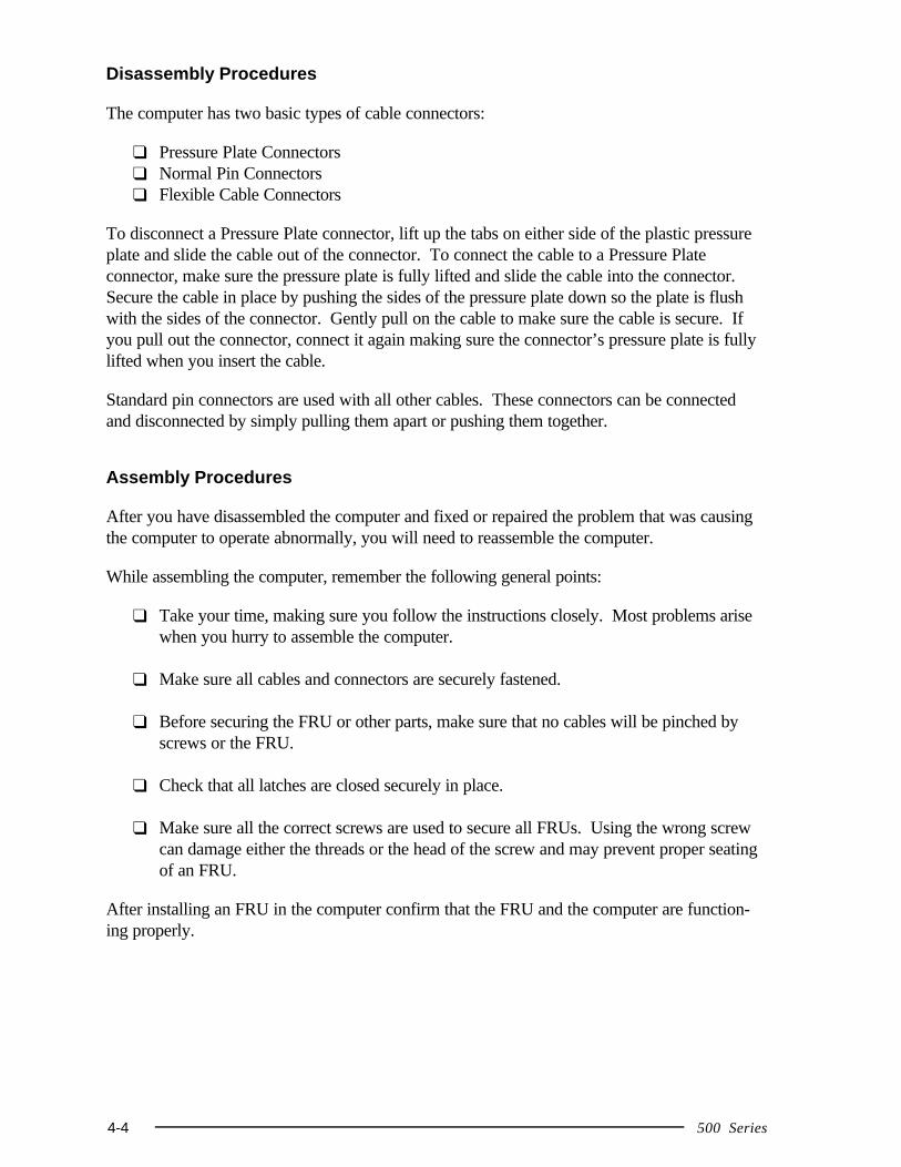
4-4 500 Series
Disassembly Procedures
The computer has two basic types of cable connectors:
❑ Pressure Plate Connectors❑ Normal Pin Connectors❑ Flexible Cable Connectors
To disconnect a Pressure Plate connector, lift up the tabs on either side of the plastic pressureplate and slide the cable out of the connector. To connect the cable to a Pressure Plateconnector, make sure the pressure plate is fully lifted and slide the cable into the connector.Secure the cable in place by pushing the sides of the pressure plate down so the plate is flushwith the sides of the connector. Gently pull on the cable to make sure the cable is secure. Ifyou pull out the connector, connect it again making sure the connector’s pressure plate is fullylifted when you insert the cable.
Standard pin connectors are used with all other cables. These connectors can be connectedand disconnected by simply pulling them apart or pushing them together.
Assembly Procedures
After you have disassembled the computer and fixed or repaired the problem that was causingthe computer to operate abnormally, you will need to reassemble the computer.
While assembling the computer, remember the following general points:
❑ Take your time, making sure you follow the instructions closely. Most problems arisewhen you hurry to assemble the computer.
❑ Make sure all cables and connectors are securely fastened.
❑ Before securing the FRU or other parts, make sure that no cables will be pinched byscrews or the FRU.
❑ Check that all latches are closed securely in place.
❑ Make sure all the correct screws are used to secure all FRUs. Using the wrong screwcan damage either the threads or the head of the screw and may prevent proper seatingof an FRU.
After installing an FRU in the computer confirm that the FRU and the computer are function-ing properly.
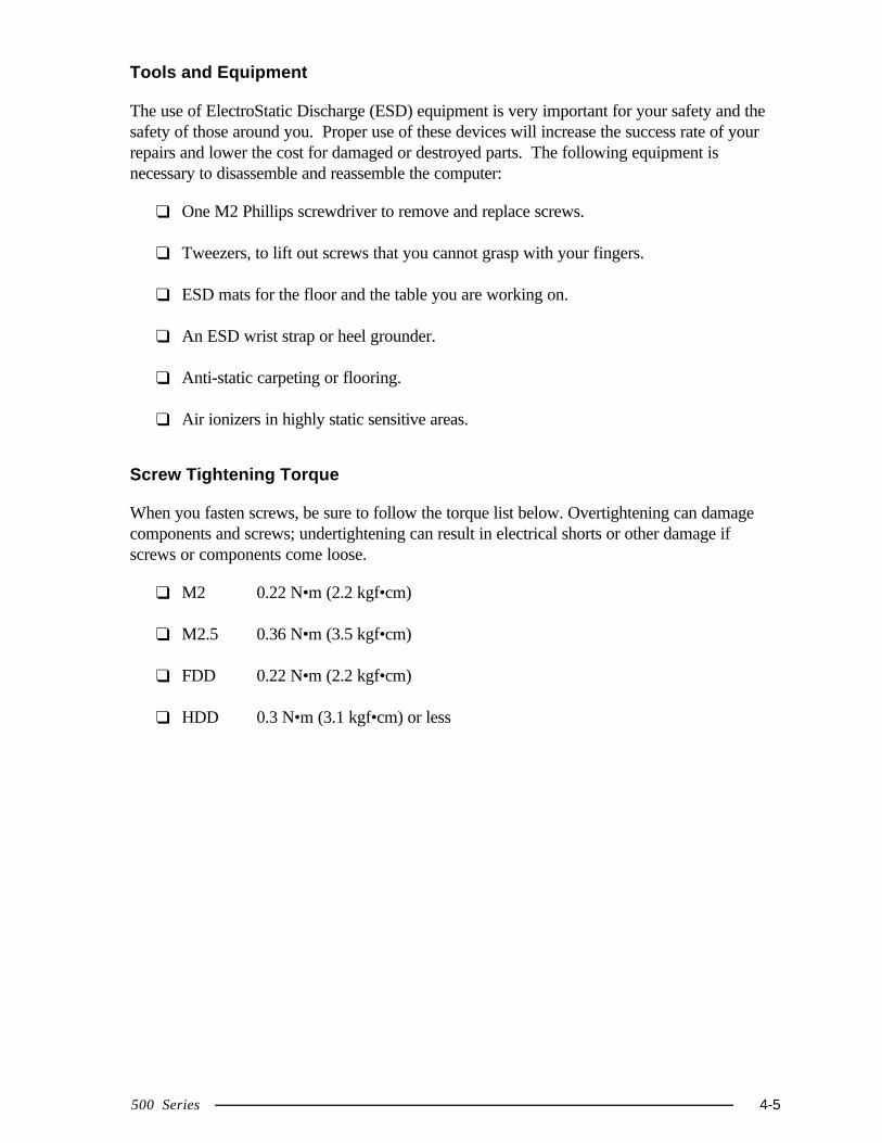
500 Series 4-5
Tools and Equipment
The use of ElectroStatic Discharge (ESD) equipment is very important for your safety and thesafety of those around you. Proper use of these devices will increase the success rate of yourrepairs and lower the cost for damaged or destroyed parts. The following equipment isnecessary to disassemble and reassemble the computer:
❑ One M2 Phillips screwdriver to remove and replace screws.
❑ Tweezers, to lift out screws that you cannot grasp with your fingers.
❑ ESD mats for the floor and the table you are working on.
❑ An ESD wrist strap or heel grounder.
❑ Anti-static carpeting or flooring.
❑ Air ionizers in highly static sensitive areas.
Screw Tightening Torque
When you fasten screws, be sure to follow the torque list below. Overtightening can damagecomponents and screws; undertightening can result in electrical shorts or other damage ifscrews or components come loose.
❑ M2 0.22 N•m (2.2 kgf•cm)
❑ M2.5 0.36 N•m (3.5 kgf•cm)
❑ FDD 0.22 N•m (2.2 kgf•cm)
❑ HDD 0.3 N•m (3.1 kgf•cm) or less
4-6 500 Series
4.2 Battery Pack
Removing the Battery Pack
To remove the battery pack, follow the steps below and refer to Figures 4-1 and 4-2.
1. Turn off the power to the computer, then disconnect the AC power cord and allexternal cables connected to the computer.
2. Turn the computer upside down.
3. Slide the battery cover lock fully in the direction of the arrow on the lock, thenslide out and remove the battery cover.
Figure 4-1 Removing the battery cover
4. Push the battery lock and the battery will pop up slightly.
5. Grasp the end of the battery and remove it.
Figure 4-2 Removing the battery pack
NOTE: For environmental reasons, do not throw away a spent battery pack. Pleasereturn spent battery packs to Toshiba.
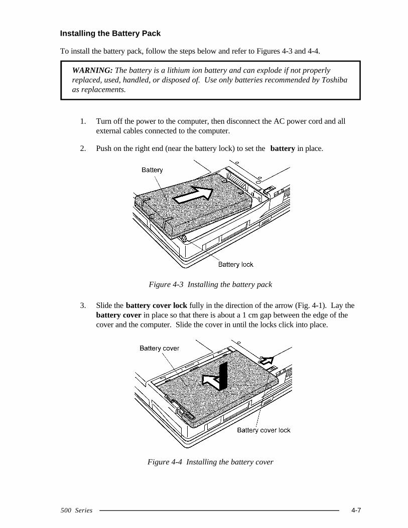
500 Series 4-7
Installing the Battery Pack
To install the battery pack, follow the steps below and refer to Figures 4-3 and 4-4.
WARNING: The battery is a lithium ion battery and can explode if not properlyreplaced, used, handled, or disposed of. Use only batteries recommended by Toshibaas replacements.
1. Turn off the power to the computer, then disconnect the AC power cord and allexternal cables connected to the computer.
2. Push on the right end (near the battery lock) to set the battery in place.
Figure 4-3 Installing the battery pack
3. Slide the battery cover lock fully in the direction of the arrow (Fig. 4-1). Lay thebattery cover in place so that there is about a 1 cm gap between the edge of thecover and the computer. Slide the cover in until the locks click into place.
Figure 4-4 Installing the battery cover
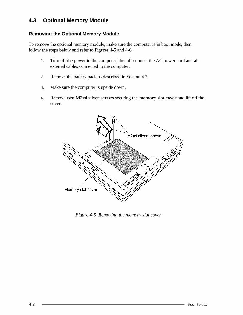
4-8 500 Series
4.3 Optional Memory Module
Removing the Optional Memory Module
To remove the optional memory module, make sure the computer is in boot mode, thenfollow the steps below and refer to Figures 4-5 and 4-6.
1. Turn off the power to the computer, then disconnect the AC power cord and allexternal cables connected to the computer.
2. Remove the battery pack as described in Section 4.2.
3. Make sure the computer is upside down.
4. Remove two M2x4 silver screws securing the memory slot cover and lift off thecover.
Figure 4-5 Removing the memory slot cover
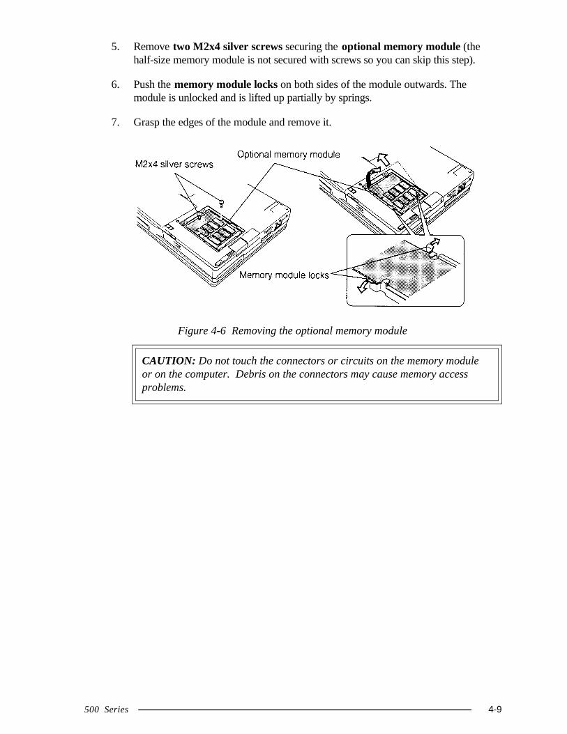
500 Series 4-9
5. Remove two M2x4 silver screws securing the optional memory module (thehalf-size memory module is not secured with screws so you can skip this step).
6. Push the memory module locks on both sides of the module outwards. Themodule is unlocked and is lifted up partially by springs.
7. Grasp the edges of the module and remove it.
Figure 4-6 Removing the optional memory module
CAUTION: Do not touch the connectors or circuits on the memory moduleor on the computer. Debris on the connectors may cause memory accessproblems.
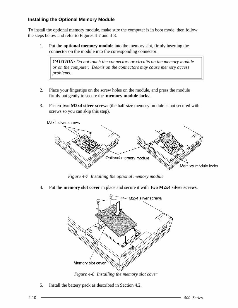
4-10 500 Series
Installing the Optional Memory Module
To install the optional memory module, make sure the computer is in boot mode, then followthe steps below and refer to Figures 4-7 and 4-8.
1. Put the optional memory module into the memory slot, firmly inserting theconnector on the module into the corresponding connector.
CAUTION: Do not touch the connectors or circuits on the memory moduleor on the computer. Debris on the connectors may cause memory accessproblems.
2. Place your fingertips on the screw holes on the module, and press the modulefirmly but gently to secure the memory module locks.
3. Fasten two M2x4 silver screws (the half-size memory module is not secured withscrews so you can skip this step).
Figure 4-7 Installing the optional memory module
4. Put the memory slot cover in place and secure it with two M2x4 silver screws.
Figure 4-8 Installing the memory slot cover
5. Install the battery pack as described in Section 4.2.
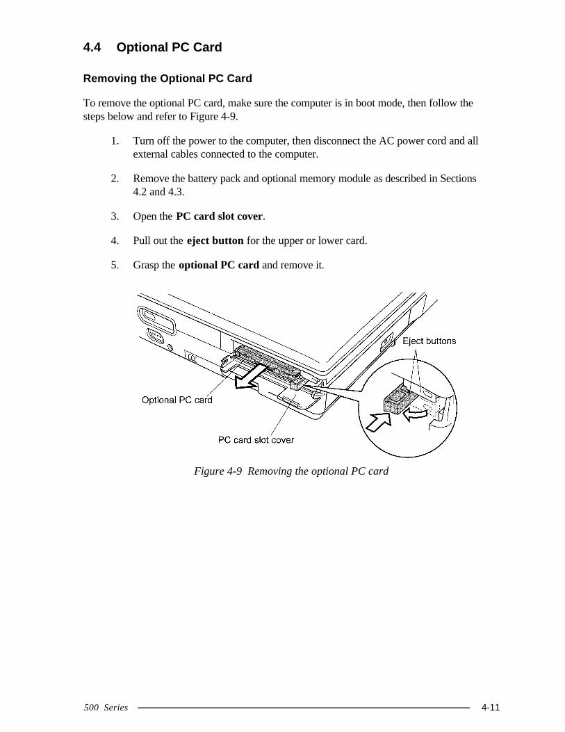
500 Series 4-11
4.4 Optional PC Card
Removing the Optional PC Card
To remove the optional PC card, make sure the computer is in boot mode, then follow thesteps below and refer to Figure 4-9.
1. Turn off the power to the computer, then disconnect the AC power cord and allexternal cables connected to the computer.
2. Remove the battery pack and optional memory module as described in Sections4.2 and 4.3.
3. Open the PC card slot cover.
4. Pull out the eject button for the upper or lower card.
5. Grasp the optional PC card and remove it.
Figure 4-9 Removing the optional PC card
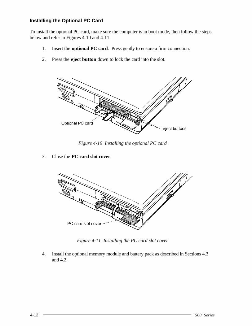
4-12 500 Series
Installing the Optional PC Card
To install the optional PC card, make sure the computer is in boot mode, then follow the stepsbelow and refer to Figures 4-10 and 4-11.
1. Insert the optional PC card. Press gently to ensure a firm connection.
2. Press the eject button down to lock the card into the slot.
Figure 4-10 Installing the optional PC card
3. Close the PC card slot cover.
Figure 4-11 Installing the PC card slot cover
4. Install the optional memory module and battery pack as described in Sections 4.3and 4.2.
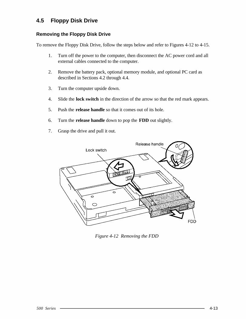
500 Series 4-13
4.5 Floppy Disk Drive
Removing the Floppy Disk Drive
To remove the Floppy Disk Drive, follow the steps below and refer to Figures 4-12 to 4-15.
1. Turn off the power to the computer, then disconnect the AC power cord and allexternal cables connected to the computer.
2. Remove the battery pack, optional memory module, and optional PC card asdescribed in Sections 4.2 through 4.4.
3. Turn the computer upside down.
4. Slide the lock switch in the direction of the arrow so that the red mark appears.
5. Push the release handle so that it comes out of its hole.
6. Turn the release handle down to pop the FDD out slightly.
7. Grasp the drive and pull it out.
Figure 4-12 Removing the FDD
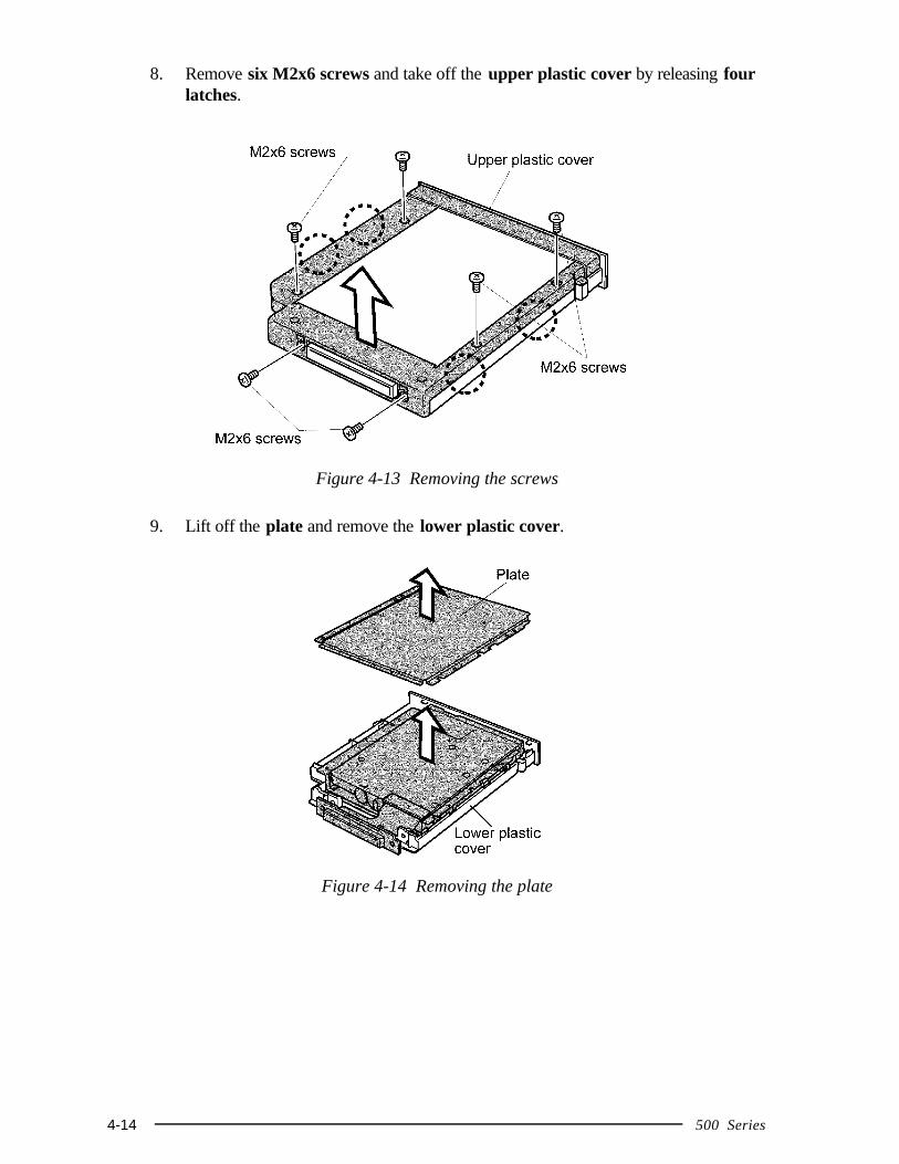
4-14 500 Series
8. Remove six M2x6 screws and take off the upper plastic cover by releasing fourlatches.
Figure 4-13 Removing the screws
9. Lift off the plate and remove the lower plastic cover.
Figure 4-14 Removing the plate

500 Series 4-15
10. Disconnect the flexible cable.
11. Remove four M2x3 screws and remove the FDD from the bracket.
Figure 4-15 Removing the bracket
Installing the Floppy Disk Drive
To install the Floppy Disk Drive, follow the steps below and refer to Figures 4-12 to 4-15.
1. Seat the FDD in the bracket and secure it with four M2x3 screws.
2. Connect the flexible cable.
3. Seat the FDD in the lower plastic cover and set the plate in place.
4. Set the upper plastic cover in place by securing the latches and fasten six M2x6screws.
5. Turn the computer upside down.
6. Insert the FDD into the slot until the release handle returns to the locked posi-tion.
7. Push the release handle back into its hole.
8. Slide the lock switch to the opposite direction of the arrow so that the red mark iscovered.
9. Install the optional PC card, optional memory module, and battery pack as de-scribed in Sections 4.4, 4.3, and 4.2.
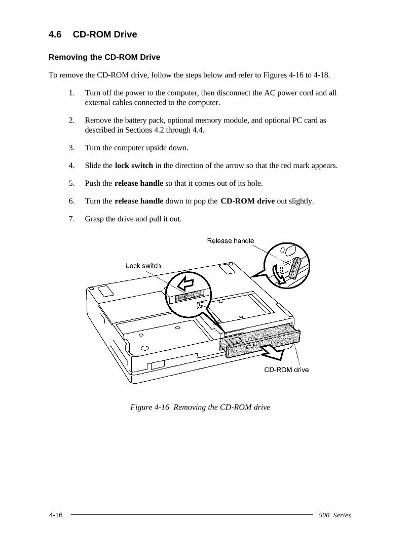
4-16 500 Series
4.6 CD-ROM Drive
Removing the CD-ROM Drive
To remove the CD-ROM drive, follow the steps below and refer to Figures 4-16 to 4-18.
1. Turn off the power to the computer, then disconnect the AC power cord and allexternal cables connected to the computer.
2. Remove the battery pack, optional memory module, and optional PC card asdescribed in Sections 4.2 through 4.4.
3. Turn the computer upside down.
4. Slide the lock switch in the direction of the arrow so that the red mark appears.
5. Push the release handle so that it comes out of its hole.
6. Turn the release handle down to pop the CD-ROM drive out slightly.
7. Grasp the drive and pull it out.
Figure 4-16 Removing the CD-ROM drive
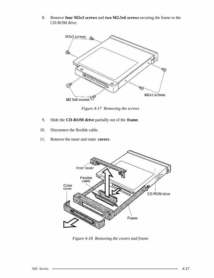
500 Series 4-17
8. Remove four M2x3 screws and two M2.5x6 screws securing the frame to theCD-ROM drive.
Figure 4-17 Removing the screws
9. Slide the CD-ROM drive partially out of the frame.
10. Disconnect the flexible cable.
11. Remove the inner and outer covers.
Figure 4-18 Removing the covers and frame
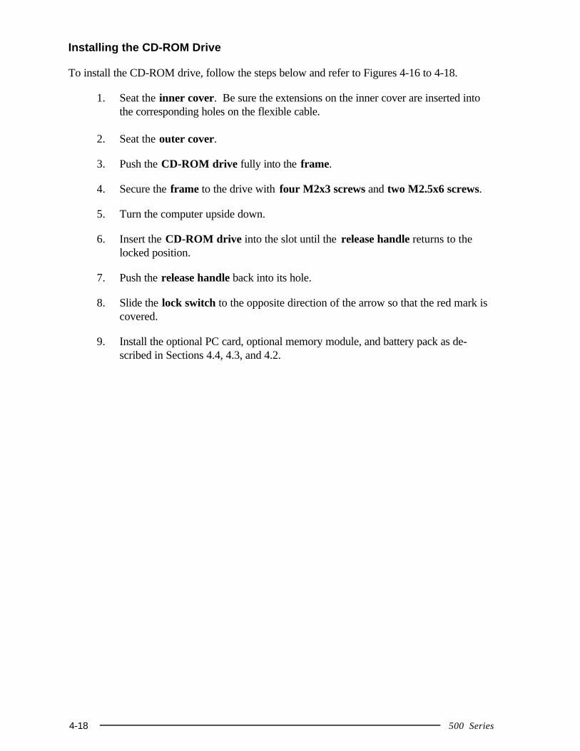
4-18 500 Series
Installing the CD-ROM Drive
To install the CD-ROM drive, follow the steps below and refer to Figures 4-16 to 4-18.
1. Seat the inner cover. Be sure the extensions on the inner cover are inserted intothe corresponding holes on the flexible cable.
2. Seat the outer cover.
3. Push the CD-ROM drive fully into the frame.
4. Secure the frame to the drive with four M2x3 screws and two M2.5x6 screws.
5. Turn the computer upside down.
6. Insert the CD-ROM drive into the slot until the release handle returns to thelocked position.
7. Push the release handle back into its hole.
8. Slide the lock switch to the opposite direction of the arrow so that the red mark iscovered.
9. Install the optional PC card, optional memory module, and battery pack as de-scribed in Sections 4.4, 4.3, and 4.2.
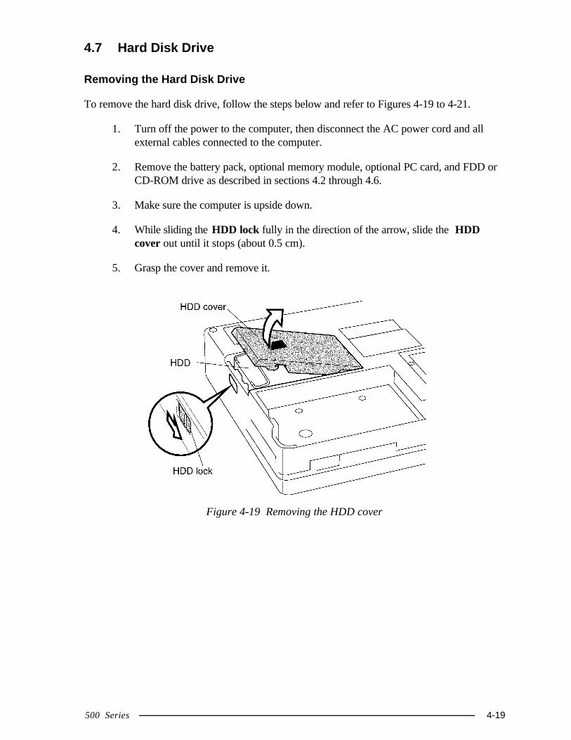
500 Series 4-19
4.7 Hard Disk Drive
Removing the Hard Disk Drive
To remove the hard disk drive, follow the steps below and refer to Figures 4-19 to 4-21.
1. Turn off the power to the computer, then disconnect the AC power cord and allexternal cables connected to the computer.
2. Remove the battery pack, optional memory module, optional PC card, and FDD orCD-ROM drive as described in sections 4.2 through 4.6.
3. Make sure the computer is upside down.
4. While sliding the HDD lock fully in the direction of the arrow, slide the HDDcover out until it stops (about 0.5 cm).
5. Grasp the cover and remove it.
Figure 4-19 Removing the HDD cover
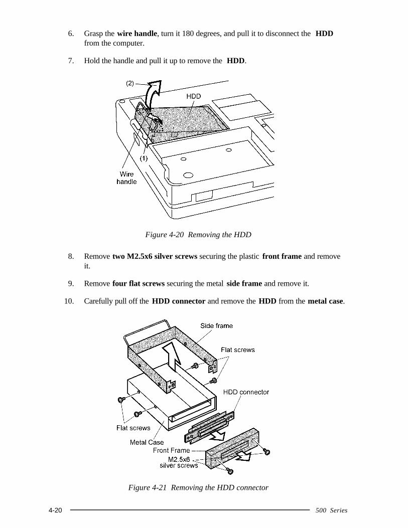
4-20 500 Series
6. Grasp the wire handle, turn it 180 degrees, and pull it to disconnect the HDDfrom the computer.
7. Hold the handle and pull it up to remove the HDD.
Figure 4-20 Removing the HDD
8. Remove two M2.5x6 silver screws securing the plastic front frame and removeit.
9. Remove four flat screws securing the metal side frame and remove it.
10. Carefully pull off the HDD connector and remove the HDD from the metal case.
Figure 4-21 Removing the HDD connector
500 Series 4-21
Installing the Hard Disk Drive
To install the hard disk drive, follow the steps below and refer to Figures 4-19 to 4-21.
1. Seat the metal case and attach the HDD connector to the HDD. Be sure to setthe position of the connector by matching the width of the HDD front with that ofthe connector. The number of the pins on the HDD is different from the numberon the connector.
CAUTION: Make sure to put the connector straight into the correspondingconnector, otherwise the connectors' pins may bend and cause problems.
2. Set the metal side frame so that its front parts are in between the folded board ofthe connector, and secure it with four flat screws.
3. Put the plastic front cover in place, making sure that its top and bottom areoriented correctly, and secure it with two M2.5x6 silver screws.
4. Make sure the computer is upside down, insert the HDD into the computer, andslide the HDD lock in the direction of the arrow to let the HDD drop into place.
5. Push the HDD to secure the HDD’s connector to the corresponding connector onthe computer.
6. Lay the HDD cover in place, being sure to leave a narrow gap (about 0.5 cm) asdescribed in step 4 of “Removing the Hard Disk Drive,” and slide the cover in untilit clicks.
7. Install the CD-ROM drive or FDD, optional PC card, optional memory module,and battery pack as described in Sections 4.6 back through 4.2.
4-22 500 Series
4.8 Second Hard Disk Drive
Removing the Second Hard Disk Drive
To remove the second hard disk drive, follow the steps below and refer to Figures 4-22 to4-25
1. Turn off the power to the computer, then disconnect the AC power cord and allexternal cables connected to the computer.
2. Remove the battery pack, optional memory module, optional PC card, and HDDas described in Sections 4.2 through 4.4, and 4.7.
3. Turn the computer upside down.
4. Slide the lock switch in the direction of the arrow so that the red mark appears.
5. Push the release handle so that it comes out of its hole.
6. Turn the release handle down to pop the second HDD out slightly.
7. Grasp the drive and pull it out.
Figure 4-22 Removing the second HDD
500 Series 4-23
8 . Remove six M2x6 screws and take off the upper plastic coverby releasing four latches.
Figure 4-23 Removing the screws
9. Lift the plate off and remove the lower plastic cover.
Figure 4-24 Removing the plate
4-24 500 Series
10. Remove four M3x4 screws securing the HDD to the lower plate and carefullydisconnect the second HDD from the flexible cable.
Figure 4-25 Removing the second HDD pack
Installing the Second Hard Disk Drive
To install the second Hard Disk Drive, follow the steps below and refer to Figures 4-22 to 4-25.
1. Attach the flexible cable to the second HDD. Be sure to set the position of theconnector.
2. Secure the lower plate with four M3x4 screws and seat it in the lower plasticcover.
3. Set the upper plate and plastic cover. Secure four latches and fasten six M2x6screws.
4. Turn the computer upside down.
5. Insert the second HDD into the slot until the release handle returns to the lockedposition.
6. Push the release handle back into its hole.
7. Slide the lock switch to the opposite direction of the arrow so that the red mark iscovered.
8. Install the HDD, optional PC card, optional memory module, and battery pack asdescribed in Sections 4.7, 4.4, 4.3, and 4.2.
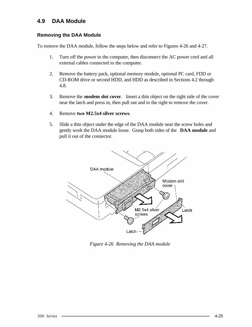
500 Series 4-25
4.9 DAA Module
Removing the DAA Module
To remove the DAA module, follow the steps below and refer to Figures 4-26 and 4-27.
1. Turn off the power to the computer, then disconnect the AC power cord and allexternal cables connected to the computer.
2. Remove the battery pack, optional memory module, optional PC card, FDD orCD-ROM drive or second HDD, and HDD as described in Sections 4.2 through4.8.
3. Remove the modem slot cover. Insert a thin object on the right side of the covernear the latch and press in, then pull out and to the right to remove the cover.
4. Remove two M2.5x4 silver screws.
5. Slide a thin object under the edge of the DAA module near the screw holes andgently work the DAA module loose. Grasp both sides of the DAA module andpull it out of the connector.
Figure 4-26 Removing the DAA module
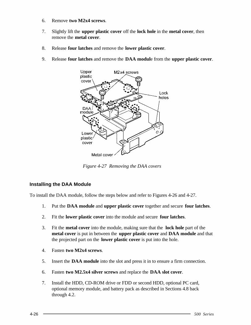
4-26 500 Series
6. Remove two M2x4 screws.
7. Slightly lift the upper plastic cover off the lock hole in the metal cover, thenremove the metal cover.
8. Release four latches and remove the lower plastic cover.
9. Release four latches and remove the DAA module from the upper plastic cover.
Figure 4-27 Removing the DAA covers
Installing the DAA Module
To install the DAA module, follow the steps below and refer to Figures 4-26 and 4-27.
1. Put the DAA module and upper plastic cover together and secure four latches.
2. Fit the lower plastic cover into the module and secure four latches.
3. Fit the metal cover into the module, making sure that the lock hole part of themetal cover is put in between the upper plastic cover and DAA module and thatthe projected part on the lower plastic cover is put into the hole.
4. Fasten two M2x4 screws.
5. Insert the DAA module into the slot and press it in to ensure a firm connection.
6. Fasten two M2.5x4 silver screws and replace the DAA slot cover.
7. Install the HDD, CD-ROM drive or FDD or second HDD, optional PC card,optional memory module, and battery pack as described in Sections 4.8 backthrough 4.2.
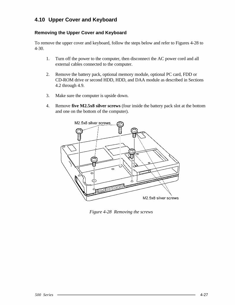
500 Series 4-27
4.10 Upper Cover and Keyboard
Removing the Upper Cover and Keyboard
To remove the upper cover and keyboard, follow the steps below and refer to Figures 4-28 to4-30.
1. Turn off the power to the computer, then disconnect the AC power cord and allexternal cables connected to the computer.
2. Remove the battery pack, optional memory module, optional PC card, FDD orCD-ROM drive or second HDD, HDD, and DAA module as described in Sections4.2 through 4.9.
3. Make sure the computer is upside down.
4. Remove five M2.5x8 silver screws (four inside the battery pack slot at the bottomand one on the bottom of the computer).
Figure 4-28 Removing the screws
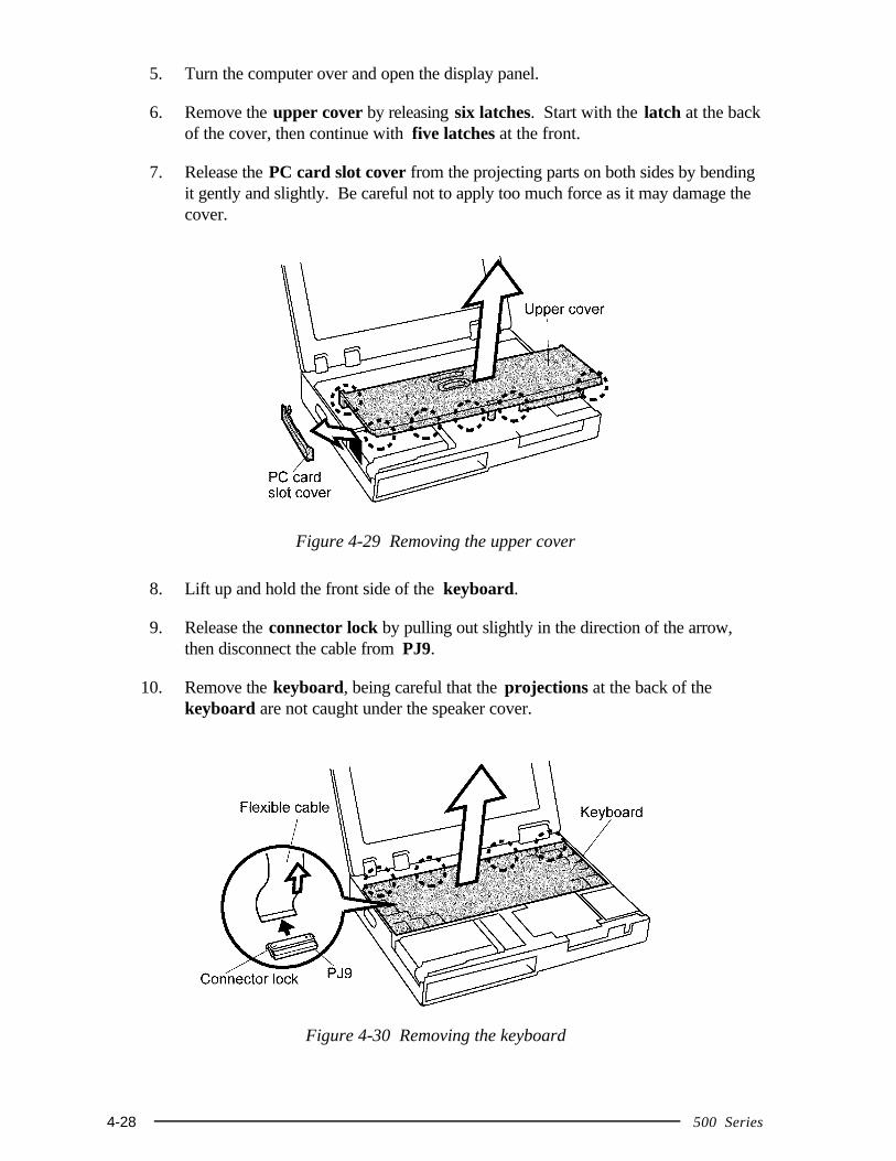
4-28 500 Series
5. Turn the computer over and open the display panel.
6. Remove the upper cover by releasing six latches. Start with the latch at the backof the cover, then continue with five latches at the front.
7. Release the PC card slot cover from the projecting parts on both sides by bendingit gently and slightly. Be careful not to apply too much force as it may damage thecover.
Figure 4-29 Removing the upper cover
8. Lift up and hold the front side of the keyboard.
9. Release the connector lock by pulling out slightly in the direction of the arrow,then disconnect the cable from PJ9.
10. Remove the keyboard, being careful that the projections at the back of thekeyboard are not caught under the speaker cover.
Figure 4-30 Removing the keyboard
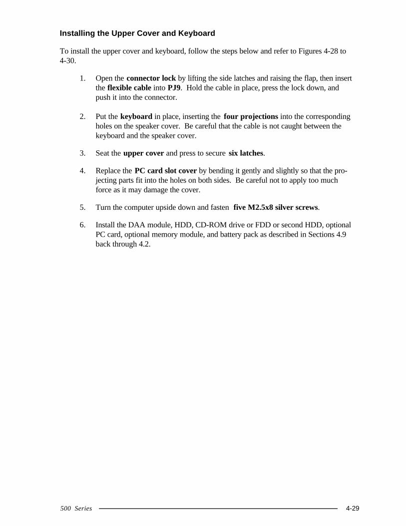
500 Series 4-29
Installing the Upper Cover and Keyboard
To install the upper cover and keyboard, follow the steps below and refer to Figures 4-28 to4-30.
1. Open the connector lock by lifting the side latches and raising the flap, then insertthe flexible cable into PJ9. Hold the cable in place, press the lock down, andpush it into the connector.
2. Put the keyboard in place, inserting the four projections into the correspondingholes on the speaker cover. Be careful that the cable is not caught between thekeyboard and the speaker cover.
3. Seat the upper cover and press to secure six latches.
4. Replace the PC card slot cover by bending it gently and slightly so that the pro-jecting parts fit into the holes on both sides. Be careful not to apply too muchforce as it may damage the cover.
5. Turn the computer upside down and fasten five M2.5x8 silver screws.
6. Install the DAA module, HDD, CD-ROM drive or FDD or second HDD, optionalPC card, optional memory module, and battery pack as described in Sections 4.9back through 4.2.
4-30 500 Series
4.11 Modem Module
Removing the Modem Module
To remove the modem module, follow the steps below and refer to Figure 4-31.
1. Turn off the power to the computer, then disconnect the AC power cord and allexternal cables connected to the computer.
2. Remove the battery pack, optional memory module, optional PC card, FDD orCD-ROM drive or second HDD, HDD, DAA module, and upper cover and key-board as described in Sections 4.2 through 4.10.
3. Remove four M2.5x6 screws and take off the metal cover.
4. Disconnect PJ601 on the modem module from PJ6 and take the module out.
Figure 4-31 Removing the modem module
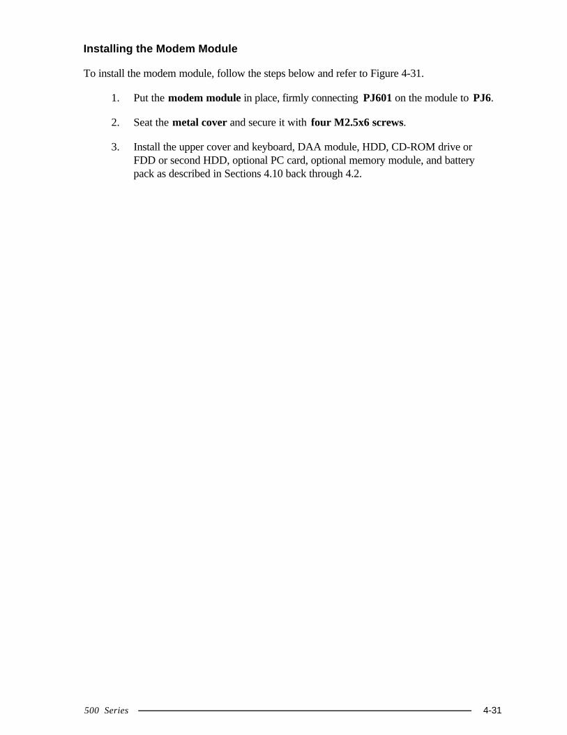
500 Series 4-31
Installing the Modem Module
To install the modem module, follow the steps below and refer to Figure 4-31.
1. Put the modem module in place, firmly connecting PJ601 on the module to PJ6.
2. Seat the metal cover and secure it with four M2.5x6 screws.
3. Install the upper cover and keyboard, DAA module, HDD, CD-ROM drive orFDD or second HDD, optional PC card, optional memory module, and batterypack as described in Sections 4.10 back through 4.2.
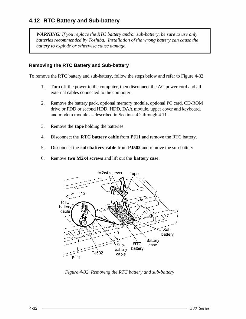
4-32 500 Series
4.12 RTC Battery and Sub-battery
WARNING: If you replace the RTC battery and/or sub-battery, be sure to use onlybatteries recommended by Toshiba. Installation of the wrong battery can cause thebattery to explode or otherwise cause damage.
Removing the RTC Battery and Sub-battery
To remove the RTC battery and sub-battery, follow the steps below and refer to Figure 4-32.
1. Turn off the power to the computer, then disconnect the AC power cord and allexternal cables connected to the computer.
2. Remove the battery pack, optional memory module, optional PC card, CD-ROMdrive or FDD or second HDD, HDD, DAA module, upper cover and keyboard,and modem module as described in Sections 4.2 through 4.11.
3. Remove the tape holding the batteries.
4. Disconnect the RTC battery cable from PJ11 and remove the RTC battery.
5. Disconnect the sub-battery cable from PJ502 and remove the sub-battery.
6. Remove two M2x4 screws and lift out the battery case.
Figure 4-32 Removing the RTC battery and sub-battery
500 Series 4-33
Installing the RTC Battery and Sub-battery
To install the RTC battery and sub-battery, follow the steps below and refer to Figure 4-32.
1. Put the battery case in place and secure it with two M2x4 screws.
2. Put the RTC battery and sub-battery in the case.
3. Carefully run the battery cables in their respective grooves on the case.
4. Connect the RTC battery cable to PJ11 and the sub-battery cable to PJ502.
5. Secure the batteries with tape.
6. Install the modem module, upper cover and keyboard, DAA module, HDD, CD-ROM drive or FDD or second HDD, optional PC card, optional memory module,and battery pack as described in Sections 4.11 back through 4.2.
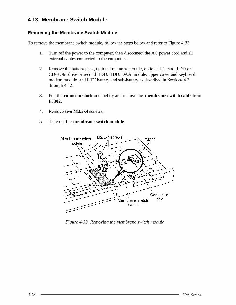
4-34 500 Series
4.13 Membrane Switch Module
Removing the Membrane Switch Module
To remove the membrane switch module, follow the steps below and refer to Figure 4-33.
1. Turn off the power to the computer, then disconnect the AC power cord and allexternal cables connected to the computer.
2. Remove the battery pack, optional memory module, optional PC card, FDD orCD-ROM drive or second HDD, HDD, DAA module, upper cover and keyboard,modem module, and RTC battery and sub-battery as described in Sections 4.2through 4.12.
3. Pull the connector lock out slightly and remove the membrane switch cable fromPJ302.
4. Remove two M2.5x4 screws.
5. Take out the membrane switch module.
Figure 4-33 Removing the membrane switch module
500 Series 4-35
Installing the Membrane Switch Module
To install the membrane switch module, follow the steps below and refer to Figure 4-33.
1. Put the membrane switch module in place and secure it with two M2.5x4screws.
2. Insert the membrane switch cable into PJ302 (into the opening between theconnector lock and the connector itself), and push in the connector lock to securethe cable.
3. Install the RTC battery and sub-battery, modem module, upper cover and key-board, DAA module, HDD, CD-ROM drive or FDD or second HDD, optional PCcard, optional memory module, and battery pack as described in Sections 4.12back through 4.2.
4-36 500 Series
4.14 CardBus Board
Removing the CardBus Board
To remove the CardBus board, follow the steps below and refer to Figure 4-34.
1. Turn off the power to the computer, then disconnect the AC power cord and allexternal cables connected to the computer.
2. Remove the battery pack, optional memory module, optional PC card, FDD orCD-ROM drive or second HDD, HDD, DAA module, upper cover and keyboard,modem module, RTC battery and sub-battery, and membrane switch module asdescribed in Sections 4.2 through 4.13.
3. Remove four M2.5x4 screws.
4. Disconnect PJ301 on the cardbus board from PJ1 and remove the board.
Figure 4-34 Removing the cardbus board
500 Series 4-37
Installing the CardBus Board
To install the cardbus board, follow the steps below and refer to Figure 4-34.
1. Put the cardbus board in place and press it gently, but firmly, to connect PJ301on the board to PJ1.
2. Secure the board with four M2.5x4 screws.
3. Install the membrane switch module, RTC battery and sub-battery, modem mod-ule, upper cover and keyboard, DAA module, HDD, CD-ROM drive or FDD orsecond HDD, optional PC card, optional memory module, and battery pack asdescribed in Sections 4.13 back through 4.2.
4-38 500 Series
4.15 Display Assembly
Removing the Display Assembly
To remove the display assembly, follow the steps below and refer to Figures 4-35 to 4-38.
1. Turn off the power to the computer, then disconnect the AC power cord and allexternal cables connected to the computer.
2. Remove the battery pack, optional memory module, optional PC card, FDD orCD-ROM drive or second HDD, HDD, DAA module, upper cover and keyboard,modem module, RTC battery and sub-battery, membrane switch module, andcardbus board as described in Sections 4.2 through 4.14.
3. Turn the computer upside down and remove one M2.5x4 silver screw (at the rearof the computer), two M2.5x6 silver screws (inside the HDD slot at the bottom),and two M2.5x8 silver screws (on the bottom of the computer).
Figure 4-35 Removing the screws
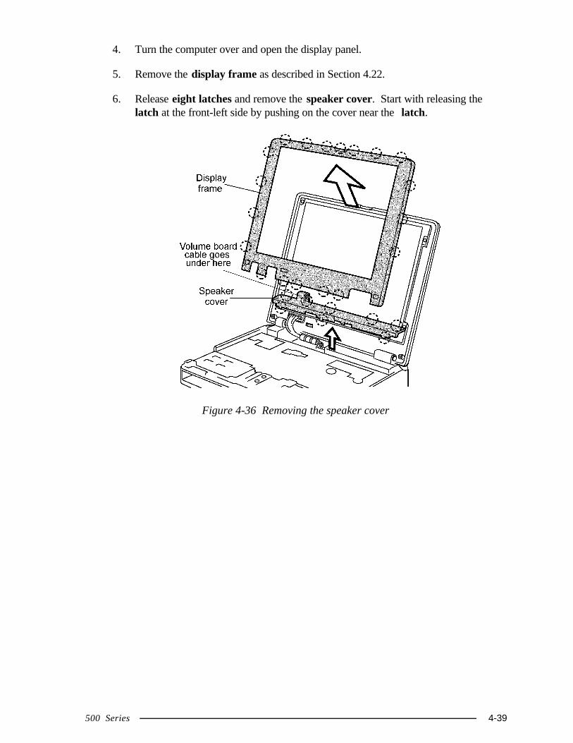
500 Series 4-39
4. Turn the computer over and open the display panel.
5. Remove the display frame as described in Section 4.22.
6. Release eight latches and remove the speaker cover. Start with releasing thelatch at the front-left side by pushing on the cover near the latch.
Figure 4-36 Removing the speaker cover
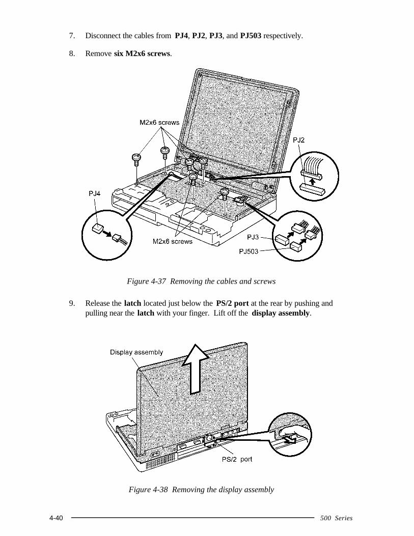
4-40 500 Series
7. Disconnect the cables from PJ4, PJ2, PJ3, and PJ503 respectively.
8. Remove six M2x6 screws.
Figure 4-37 Removing the cables and screws
9. Release the latch located just below the PS/2 port at the rear by pushing andpulling near the latch with your finger. Lift off the display assembly.
Figure 4-38 Removing the display assembly
500 Series 4-41
Installing the Display Assembly
To install the display assembly, follow the steps below and refer to Figures 4-35 to 4-38.
1. Put the display assembly in place and secure it with the latch at the rear.
2. Fasten six M2x6 screws.
3. Connect the cables to PJ4, PJ2, PJ3, and PJ503 respectively.
4. Put the speaker cover in place and secure it with eight latches. Start with thefront latches. Be sure to thread the volume board cable carefully. It should laysmoothly under the "hump" on the speaker cover.
5. Install the display frame as described in Section 4.22.
6. Close the display panel and turn the computer upside down.
7. Fasten one M2.5x4 silver screw at the rear, and two M2.5x6 silver screws andtwo M2.5x8 silver screws on the bottom of the computer.
8. Install the cardbus board, membrane switch module, RTC battery and sub-battery,modem module, upper cover and keyboard, DAA module, HDD, CD-ROM driveor FDD or second HDD, optional PC card, optional memory module, and batterypack as described in Sections 4.14 back through 4.2.
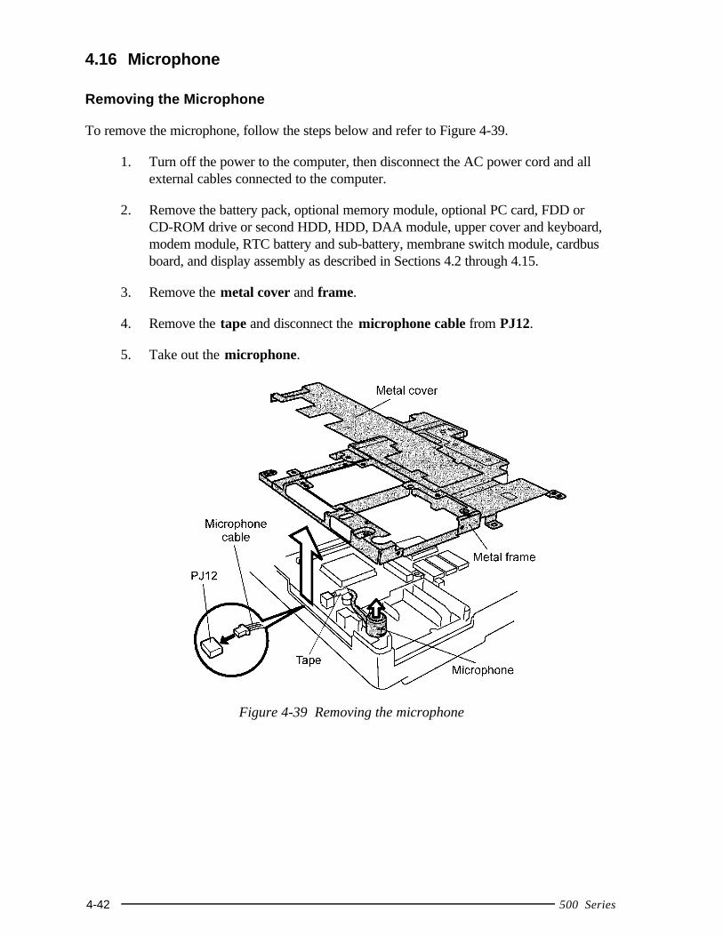
4-42 500 Series
4.16 Microphone
Removing the Microphone
To remove the microphone, follow the steps below and refer to Figure 4-39.
1. Turn off the power to the computer, then disconnect the AC power cord and allexternal cables connected to the computer.
2. Remove the battery pack, optional memory module, optional PC card, FDD orCD-ROM drive or second HDD, HDD, DAA module, upper cover and keyboard,modem module, RTC battery and sub-battery, membrane switch module, cardbusboard, and display assembly as described in Sections 4.2 through 4.15.
3. Remove the metal cover and frame.
4. Remove the tape and disconnect the microphone cable from PJ12.
5. Take out the microphone.
Figure 4-39 Removing the microphone
500 Series 4-43
Installing the Microphone
To install the microphone, follow the steps below and refer to Figure 4-39.
1. Put the microphone in place so that the two projecting parts on the computer areinserted into the holes of the microphone’s rubber cushion.
2. Connect the microphone cable to PJ12.
3. Put the metal cover and frame in place.
4. Install the display assembly, cardbus board, membrane switch module, RTC bat-tery and sub-battery, modem module, upper cover and keyboard, DAA module,HDD, CD-ROM drive or FDD or second HDD, optional PC card, optionalmemory module, and battery pack as described in Sections 4.15 back through 4.2.
4-44 500 Series
4.17 Sound Board
Removing the Sound Board
To remove the sound board, follow the steps below and refer to Figure 4-40.
1. Turn off the power to the computer, then disconnect the AC power cord and allexternal cables connected to the computer.
2. Remove the battery pack, optional memory module, optional PC card, FDD orCD-ROM drive or second HDD, HDD, DAA module, upper cover and keyboard,modem module, RTC battery and sub-battery, membrane switch module, cardbusboard, display assembly, and microphone as described in Sections 4.2 through4.16.
3. Remove one M2.5x6 screw and take off the metal cover.
4. Push the connector lock up to release the sound board cable and pull the cableout.
5. Remove the sound board and disconnect PJ11 on the board from PJ8. Whenremoving the board be careful that the projecting parts on the board, such as thecontrol dial, are not caught in between the computer frame.
Figure 4-40 Removing the sound board
500 Series 4-45
Installing the Sound Board
To install the sound board, follow the steps below and refer to Figure 4-40.
1. Put the sound board in place. With the computer frame pulled out slightly insertthe projecting parts on the board, such as the control dial, into the correspondingholes on the computer frame. Press the board gently but firmly to connect PJ11on the board to PJ8.
2. Insert the sound board cable into the connector and secure it by pushing theconnector lock down.
3. Put the metal cover in place and secure it with one M2.5x6 screw.
4. Install the display assembly, microphone, cardbus board, membrane switch mod-ule, RTC battery and sub-battery, modem module, upper cover and keyboard,DAA module, HDD, CD-ROM drive or FDD or second HDD, optional PC card,optional memory module, and battery pack as described in Sections 4.16 backthrough 4.2.
4-46 500 Series
4.18 Flat Cable
Removing the Flat Cable
To remove the flat cable, follow the steps below and refer to Figure 4-41.
1. Turn off the power to the computer, then disconnect the AC power cord and allexternal cables connected to the computer.
2. Remove the battery pack, optional memory module, optional PC card, FDD orCD-ROM drive or second HDD, DAA module, HDD, upper cover and keyboard,modem module, RTC battery and sub-battery, membrane switch module, cardbusboard, display assembly, microphone, and sound board as described in Sections 4.2through 4.17.
3. Push the connector lock up and disconnect the flat cable from PJ7.
Figure 4-41 Removing the flat cable
500 Series 4-47
Installing the Flat Cable
To install the flat cable, follow the steps below and refer to Figure 4-41.
1. Insert the flat cable into PJ7 and secure it by pushing down on the connectorlock. Be sure the blue-printed side is facing up.
2. Install the sound board, microphone, display assembly, cardbus board, membraneswitch module, RTC battery and sub-battery, modem module, upper cover andkeyboard, DAA module, HDD, CD-ROM drive or FDD or second HDD, optionalPC card, optional memory module, and battery pack as described in Sections 4.17back through 4.2.
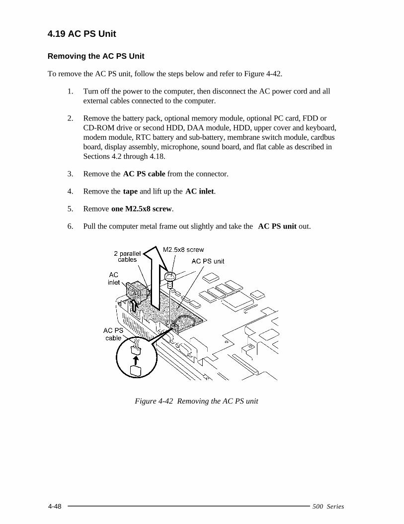
4-48 500 Series
4.19 AC PS Unit
Removing the AC PS Unit
To remove the AC PS unit, follow the steps below and refer to Figure 4-42.
1. Turn off the power to the computer, then disconnect the AC power cord and allexternal cables connected to the computer.
2. Remove the battery pack, optional memory module, optional PC card, FDD orCD-ROM drive or second HDD, DAA module, HDD, upper cover and keyboard,modem module, RTC battery and sub-battery, membrane switch module, cardbusboard, display assembly, microphone, sound board, and flat cable as described inSections 4.2 through 4.18.
3. Remove the AC PS cable from the connector.
4. Remove the tape and lift up the AC inlet.
5. Remove one M2.5x8 screw.
6. Pull the computer metal frame out slightly and take the AC PS unit out.
Figure 4-42 Removing the AC PS unit
500 Series 4-49
Installing the AC PS Unit
To install the AC PS unit, follow the steps below and refer to Figure 4-42.
1. Put the AC PS unit in place and secure it with one M2.5x8 screw.
2. Set the AC inlet so that the computer metal frame is in the openings between thefront part and side wings of the AC inlet. Make sure that the two cables runparallel to each other; they should not cross.
3. Replace the tape.
4. Insert the AC PS cable into the connector.
5. Install the flat cable, sound board, microphone, display assembly, cardbus board,membrane switch module, RTC battery and sub-battery, modem module, uppercover and keyboard, DAA module, HDD, CD-ROM drive or FDD or secondHDD, optional PC card, optional memory module, and battery pack as describedin Sections 4.18 back through 4.2.
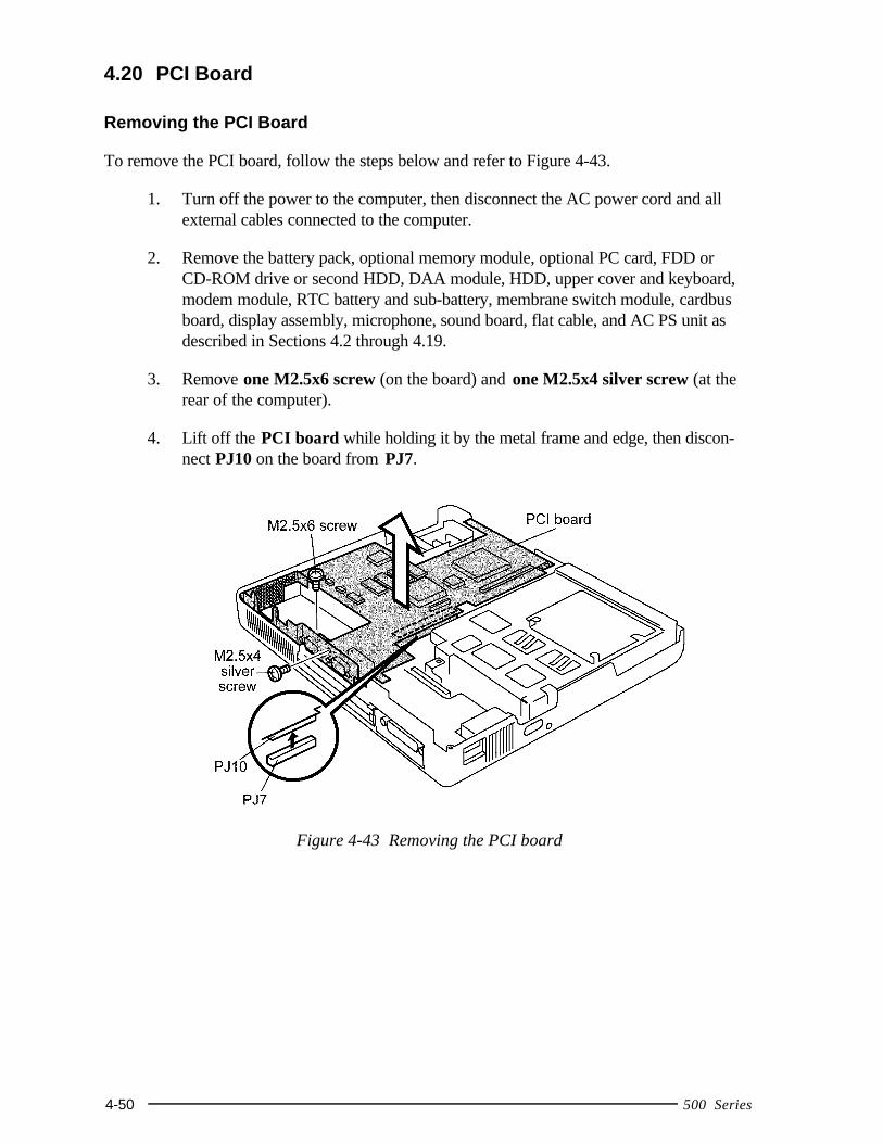
4-50 500 Series
4.20 PCI Board
Removing the PCI Board
To remove the PCI board, follow the steps below and refer to Figure 4-43.
1. Turn off the power to the computer, then disconnect the AC power cord and allexternal cables connected to the computer.
2. Remove the battery pack, optional memory module, optional PC card, FDD orCD-ROM drive or second HDD, DAA module, HDD, upper cover and keyboard,modem module, RTC battery and sub-battery, membrane switch module, cardbusboard, display assembly, microphone, sound board, flat cable, and AC PS unit asdescribed in Sections 4.2 through 4.19.
3. Remove one M2.5x6 screw (on the board) and one M2.5x4 silver screw (at therear of the computer).
4. Lift off the PCI board while holding it by the metal frame and edge, then discon-nect PJ10 on the board from PJ7.
Figure 4-43 Removing the PCI board
500 Series 4-51
Installing the PCI Board
To install the PCI board, follow the steps below and refer to Figure 4-43.
1. Put the PCI board in place, firmly connecting PJ10 on the board to PJ7.
2. Fasten one M2.5x6 screw and one M2.5x4 silver screw to secure the board.
3. Install the AC PS unit, flat cable, sound board, microphone, display assembly,cardbus board, membrane switch module, RTC battery and sub-battery, modemmodule, upper cover and keyboard, DAA module, HDD, CD-ROM drive or FDDor second HDD, optional PC card, optional memory module, and battery pack asdescribed in Sections 4.19 back through 4.2.
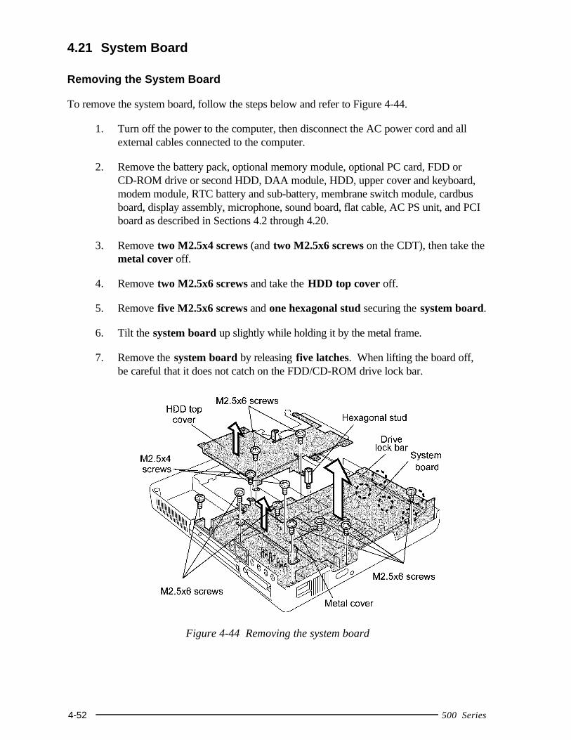
4-52 500 Series
4.21 System Board
Removing the System Board
To remove the system board, follow the steps below and refer to Figure 4-44.
1. Turn off the power to the computer, then disconnect the AC power cord and allexternal cables connected to the computer.
2. Remove the battery pack, optional memory module, optional PC card, FDD orCD-ROM drive or second HDD, DAA module, HDD, upper cover and keyboard,modem module, RTC battery and sub-battery, membrane switch module, cardbusboard, display assembly, microphone, sound board, flat cable, AC PS unit, and PCIboard as described in Sections 4.2 through 4.20.
3. Remove two M2.5x4 screws (and two M2.5x6 screws on the CDT), then take themetal cover off.
4. Remove two M2.5x6 screws and take the HDD top cover off.
5. Remove five M2.5x6 screws and one hexagonal stud securing the system board.
6. Tilt the system board up slightly while holding it by the metal frame.
7. Remove the system board by releasing five latches. When lifting the board off,be careful that it does not catch on the FDD/CD-ROM drive lock bar.
Figure 4-44 Removing the system board
500 Series 4-53
Installing the System Board
To install the system board, follow the steps below and refer to Figure 4-44.
1. Put the system board in place and secure the latches. When placing the board,make sure that the FDD/CD-ROM drive lock bar is put through the hole on theboard.
2. Fasten five M2.5x6 screws and one hexagonal stud to secure the board.
3. Put the HDD top cover in place and secure it with two M2.5x6 screws.
4. Put the metal cover in place and secure it with two M2.5x4 screws (and twoM2.5x6 screws on the CDT).
5. Install the PCI board, AC PS unit, flat cable, sound board, microphone, displayassembly, cardbus board, membrane switch module, RTC battery and sub-battery,modem module, upper cover and keyboard, DAA module, HDD, CD-ROM driveor FDD or second HDD, optional PC card, optional memory module, and batterypack as described in Sections 4.20 back through 4.2.
4-54 500 Series
4.22 Display Frame
Removing the Display Frame
To remove the display frame, follow the steps below and refer to Figure 4-45 (the illustrationis based on the STN display screen, but the procedure is the same for the TFT display screen).
1. Turn off the power to the computer, then disconnect the AC power cord and allexternal cables connected to the computer.
2. Remove the battery pack as described in Section 4.2.
3. Remove two seals and two M2.5x6 screws. When removing them, support thedisplay panel by the back so it will not be damaged.
4. Carefully insert your fingers between the display frame (inner side) and the LCDpanel, and pull out the frame to release nineteen latches (four at the left side,three at the right side, five at the lower side, and seven at the upper side). Startwith the latches at the left and right sides.
Figure 4-45 Removing the display frame (STN display screen)
500 Series 4-55
Installing the Display Frame
To install the display frame, follow the steps below and refer to Figure 4-45 (the illustration isbased on the STN display screen, but the procedure is the same for the TFT display screen).
1. Put the display frame in place and secure the latches.
2. Fasten two M2.5x6 screws and attach two seals. When fastening them, supportthe display panel by the back so it will not be damaged.
3. Install the battery pack as described in Section 4.2.
NOTE: The speaker cover must be in place before you install the display frame. SeeSection 4.15, Display Assembly.
4-56 500 Series
4.23 FL Inverter Board
Removing the FL Inverter Board
To remove the FL inverter board, follow the steps below and refer to Figure 4-46 (the illustra-tion is based on the STN display screen, but the procedure is the same for the TFT displayscreen).
1. Turn off the power to the computer, then disconnect the AC power cord and allexternal cables connected to the computer.
2. Remove the battery pack and display frame as described in Sections 4.2 and 4.22.
3. Remove two M2.5x6 screws. When removing them, support the display panel bythe back so it will not be damaged.
4. Lift up the plastic protector and raise the FL inverter board slightly, then discon-nect the FL inverter cable from CN1 and the FL cable from CN2 (in that order).
Figure 4-46 Removing the FL inverter board (STN display screen)
500 Series 4-57
Installing the FL inverter board
To install the FL inverter board, follow the steps below and refer to Figure 4-46 (the illustra-tion is based on the STN display screen, but the procedure is the same for the TFT displayscreen).
1. Connect the FL cable to CN2 first, then connect the FL inverter cable to CN1.
2. Put the FL inverter board in place and secure it with two M2.5x6 screws. Whenfastening the screws, support the display panel by the back so it will not be dam-aged.
3. Install the display frame and battery pack as described in Sections 4.22 and 4.2.
4-58 500 Series
4.24 LCD Module
Removing the LCD Module
To remove the LCD module, follow the steps below and refer to Figure 4.47 (the illustrationis based on the STN display screen, but the procedure is the same for the TFT display screen).
1. Turn off the power to the computer, then disconnect the AC power cord and allexternal cables connected to the computer.
2. Remove the battery pack, display frame, and FL inverter board as described inSections 4.2, 4.22, and 4.23.
3. Remove four M2.5x6 screws. When removing them, support the display panel bythe back so it will not be damaged.
4. Disconnect the LCD cable from the connector (the connector position of the TFTdisplay screen is not exactly the same as illustrated, but the location is the same),and lift off the LCD module.
Figure 4-47 Removing the LCD module (STN display screen)
500 Series 4-59
Installing the LCD Module
To install the LCD module, follow the steps below and refer to Figure 4-47 (the illustration isbased on the STN display screen, but the procedure is the same for the TFT display screen).
1. Connect the LCD cable (the connector position of the TFT display screen is notthe same as illustrated).
2. Seat the LCD module and secure it with four M2.5x6 screws. When fasteningthe screws, support the display panel by the back so it will not be damaged.
3. Install the FL inverter board, display frame, and battery pack as described inSections 4.23, 4.22, and 4.2.
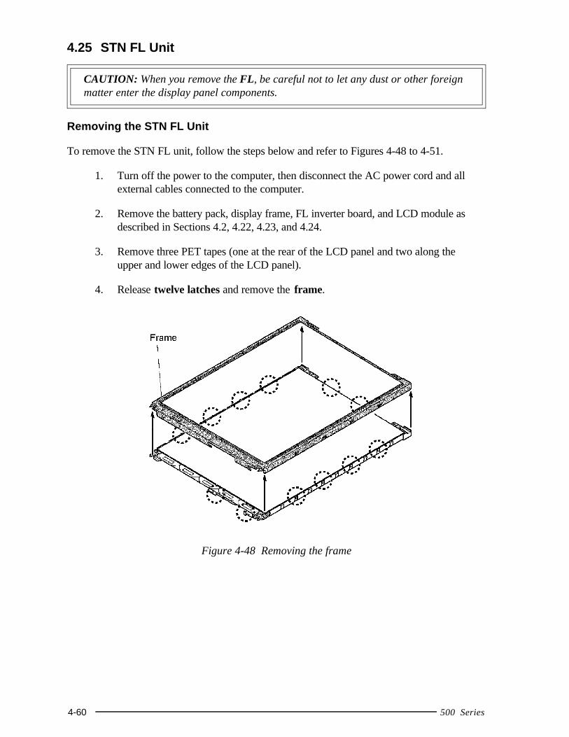
4-60 500 Series
4.25 STN FL Unit
CAUTION: When you remove the FL, be careful not to let any dust or other foreignmatter enter the display panel components.
Removing the STN FL Unit
To remove the STN FL unit, follow the steps below and refer to Figures 4-48 to 4-51.
1. Turn off the power to the computer, then disconnect the AC power cord and allexternal cables connected to the computer.
2. Remove the battery pack, display frame, FL inverter board, and LCD module asdescribed in Sections 4.2, 4.22, 4.23, and 4.24.
3. Remove three PET tapes (one at the rear of the LCD panel and two along theupper and lower edges of the LCD panel).
4. Release twelve latches and remove the frame.
Figure 4-48 Removing the frame
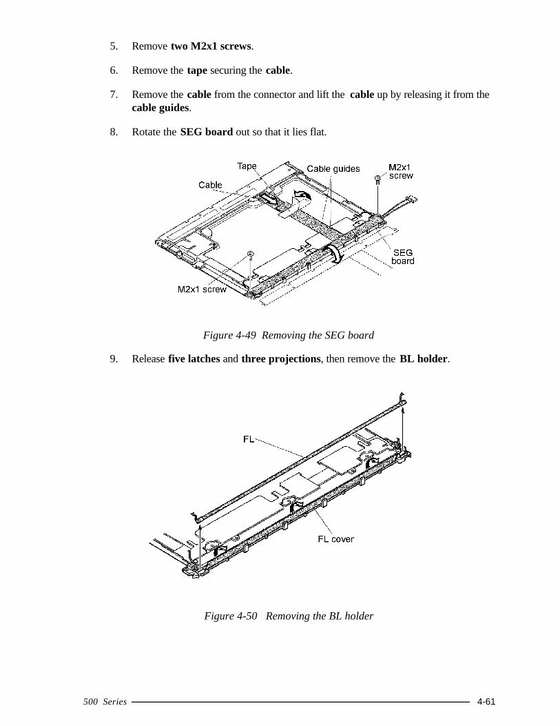
500 Series 4-61
5. Remove two M2x1 screws.
6. Remove the tape securing the cable.
7. Remove the cable from the connector and lift the cable up by releasing it from thecable guides.
8. Rotate the SEG board out so that it lies flat.
Figure 4-49 Removing the SEG board
9. Release five latches and three projections, then remove the BL holder.
Figure 4-50 Removing the BL holder
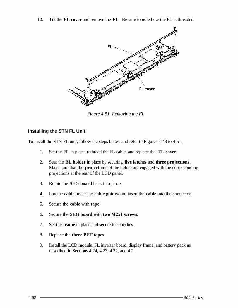
4-62 500 Series
10. Tilt the FL cover and remove the FL. Be sure to note how the FL is threaded.
Figure 4-51 Removing the FL
Installing the STN FL Unit
To install the STN FL unit, follow the steps below and refer to Figures 4-48 to 4-51.
1. Set the FL in place, rethread the FL cable, and replace the FL cover.
2. Seat the BL holder in place by securing five latches and three projections.Make sure that the projections of the holder are engaged with the correspondingprojections at the rear of the LCD panel.
3. Rotate the SEG board back into place.
4. Lay the cable under the cable guides and insert the cable into the connector.
5. Secure the cable with tape.
6. Secure the SEG board with two M2x1 screws.
7. Set the frame in place and secure the latches.
8. Replace the three PET tapes.
9. Install the LCD module, FL inverter board, display frame, and battery pack asdescribed in Sections 4.24, 4.23, 4.22, and 4.2.
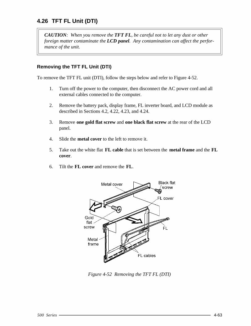
500 Series 4-63
4.26 TFT FL Unit (DTI)
CAUTION: When you remove the TFT FL, be careful not to let any dust or otherforeign matter contaminate the LCD panel. Any contamination can affect the perfor-mance of the unit.
Removing the TFT FL Unit (DTI)
To remove the TFT FL unit (DTI), follow the steps below and refer to Figure 4-52.
1. Turn off the power to the computer, then disconnect the AC power cord and allexternal cables connected to the computer.
2. Remove the battery pack, display frame, FL inverter board, and LCD module asdescribed in Sections 4.2, 4.22, 4.23, and 4.24.
3. Remove one gold flat screw and one black flat screw at the rear of the LCDpanel.
4. Slide the metal cover to the left to remove it.
5. Take out the white flat FL cable that is set between the metal frame and the FLcover.
6. Tilt the FL cover and remove the FL.
Figure 4-52 Removing the TFT FL (DTI)
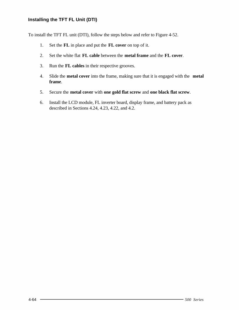
4-64 500 Series
Installing the TFT FL Unit (DTI)
To install the TFT FL unit (DTI), follow the steps below and refer to Figure 4-52.
1. Set the FL in place and put the FL cover on top of it.
2. Set the white flat FL cable between the metal frame and the FL cover.
3. Run the FL cables in their respective grooves.
4. Slide the metal cover into the frame, making sure that it is engaged with the metalframe.
5. Secure the metal cover with one gold flat screw and one black flat screw.
6. Install the LCD module, FL inverter board, display frame, and battery pack asdescribed in Sections 4.24, 4.23, 4.22, and 4.2.
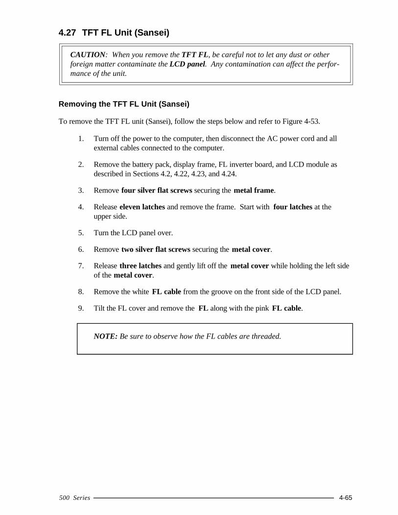
500 Series 4-65
4.27 TFT FL Unit (Sansei)
CAUTION: When you remove the TFT FL, be careful not to let any dust or otherforeign matter contaminate the LCD panel. Any contamination can affect the perfor-mance of the unit.
Removing the TFT FL Unit (Sansei)
To remove the TFT FL unit (Sansei), follow the steps below and refer to Figure 4-53.
1. Turn off the power to the computer, then disconnect the AC power cord and allexternal cables connected to the computer.
2. Remove the battery pack, display frame, FL inverter board, and LCD module asdescribed in Sections 4.2, 4.22, 4.23, and 4.24.
3. Remove four silver flat screws securing the metal frame.
4. Release eleven latches and remove the frame. Start with four latches at theupper side.
5. Turn the LCD panel over.
6. Remove two silver flat screws securing the metal cover.
7. Release three latches and gently lift off the metal cover while holding the left sideof the metal cover.
8. Remove the white FL cable from the groove on the front side of the LCD panel.
9. Tilt the FL cover and remove the FL along with the pink FL cable.
NOTE: Be sure to observe how the FL cables are threaded.
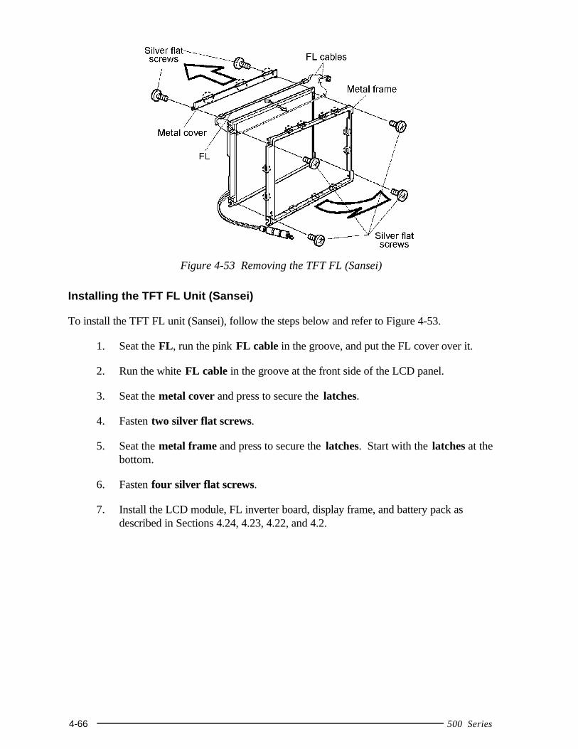
4-66 500 Series
Figure 4-53 Removing the TFT FL (Sansei)
Installing the TFT FL Unit (Sansei)
To install the TFT FL unit (Sansei), follow the steps below and refer to Figure 4-53.
1. Seat the FL, run the pink FL cable in the groove, and put the FL cover over it.
2. Run the white FL cable in the groove at the front side of the LCD panel.
3. Seat the metal cover and press to secure the latches.
4. Fasten two silver flat screws.
5. Seat the metal frame and press to secure the latches. Start with the latches at thebottom.
6. Fasten four silver flat screws.
7. Install the LCD module, FL inverter board, display frame, and battery pack asdescribed in Sections 4.24, 4.23, 4.22, and 4.2.
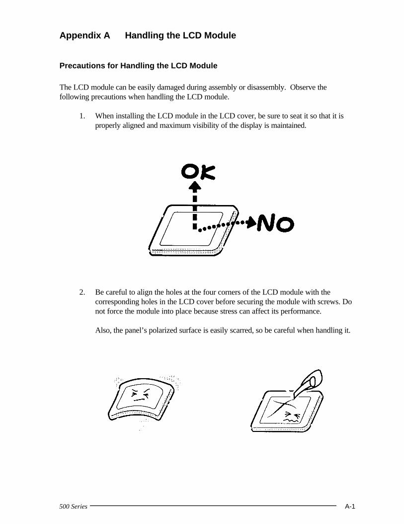
500 Series A-1
Appendix A Handling the LCD Module
Precautions for Handling the LCD Module
The LCD module can be easily damaged during assembly or disassembly. Observe thefollowing precautions when handling the LCD module.
1. When installing the LCD module in the LCD cover, be sure to seat it so that it isproperly aligned and maximum visibility of the display is maintained.
2. Be careful to align the holes at the four corners of the LCD module with thecorresponding holes in the LCD cover before securing the module with screws. Donot force the module into place because stress can affect its performance.
Also, the panel’s polarized surface is easily scarred, so be careful when handling it.
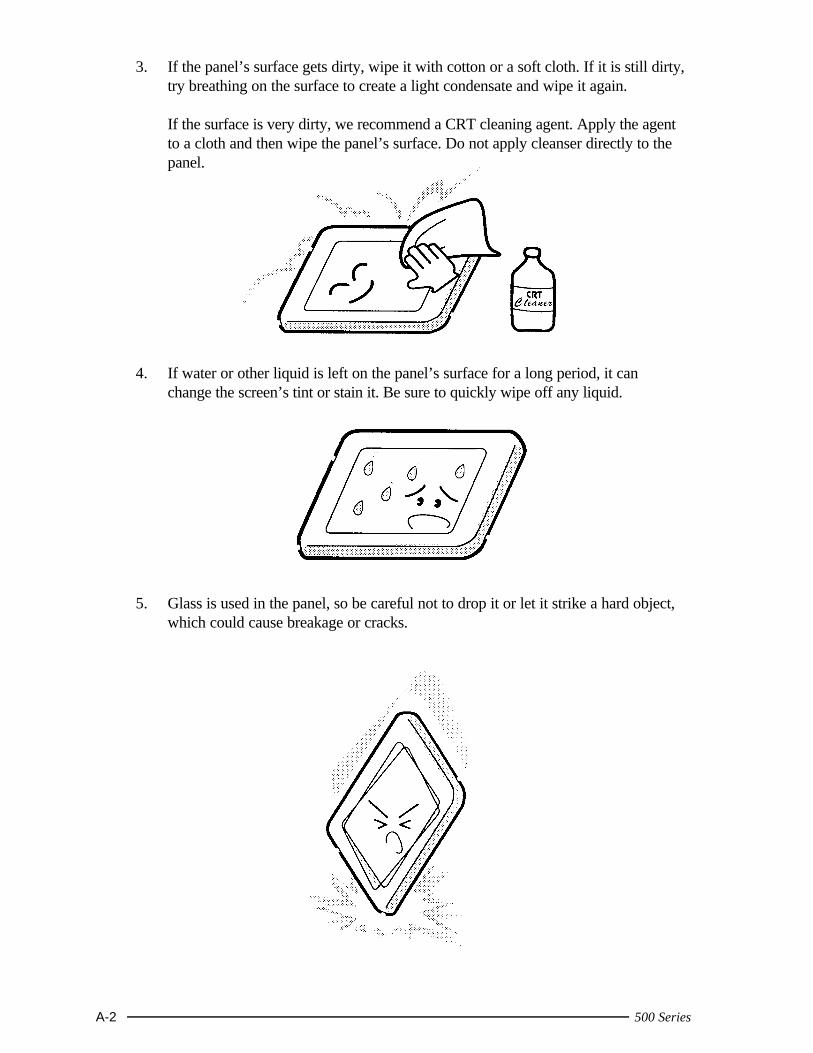
A-2 500 Series
3. If the panel’s surface gets dirty, wipe it with cotton or a soft cloth. If it is still dirty,try breathing on the surface to create a light condensate and wipe it again.
If the surface is very dirty, we recommend a CRT cleaning agent. Apply the agentto a cloth and then wipe the panel’s surface. Do not apply cleanser directly to thepanel.
4. If water or other liquid is left on the panel’s surface for a long period, it canchange the screen’s tint or stain it. Be sure to quickly wipe off any liquid.
5. Glass is used in the panel, so be careful not to drop it or let it strike a hard object,which could cause breakage or cracks.
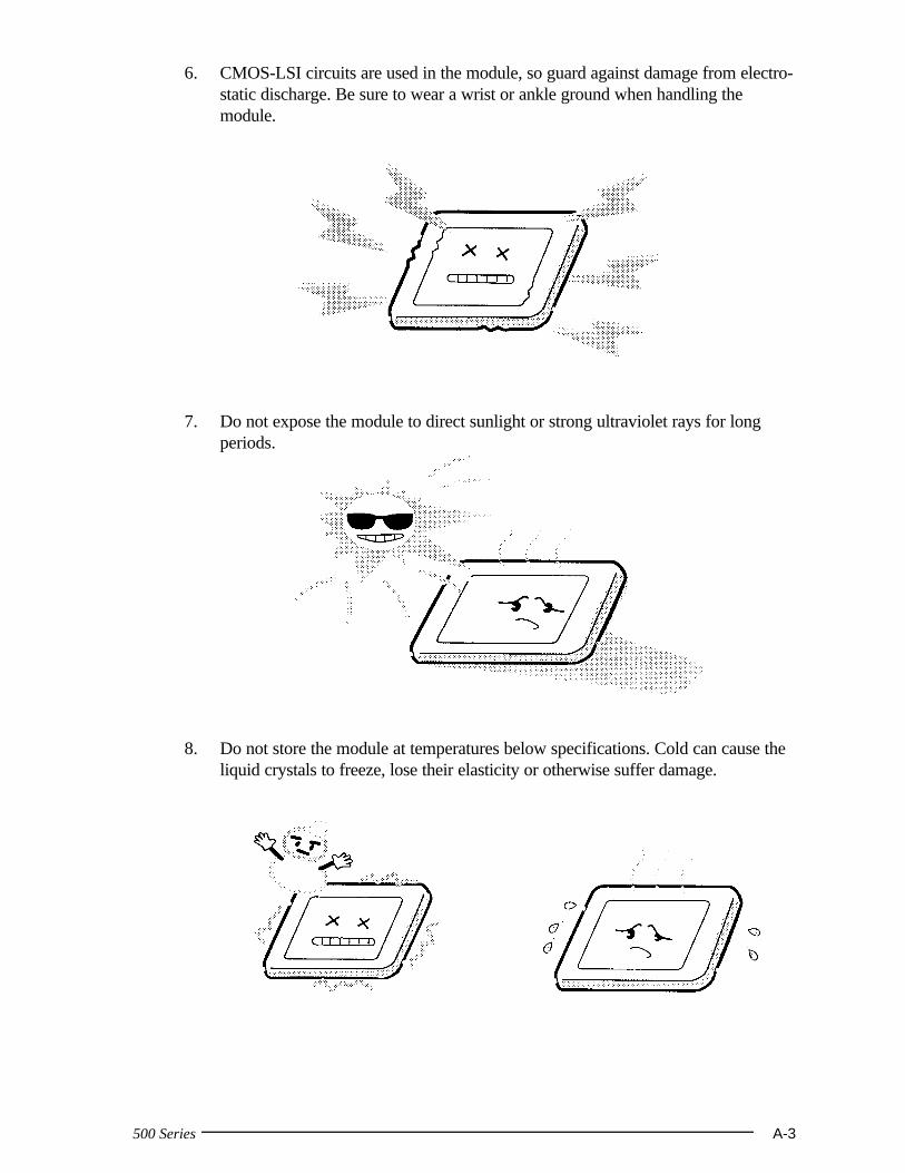
500 Series A-3
6. CMOS-LSI circuits are used in the module, so guard against damage from electro-static discharge. Be sure to wear a wrist or ankle ground when handling themodule.
7. Do not expose the module to direct sunlight or strong ultraviolet rays for longperiods.
8. Do not store the module at temperatures below specifications. Cold can cause theliquid crystals to freeze, lose their elasticity or otherwise suffer damage.
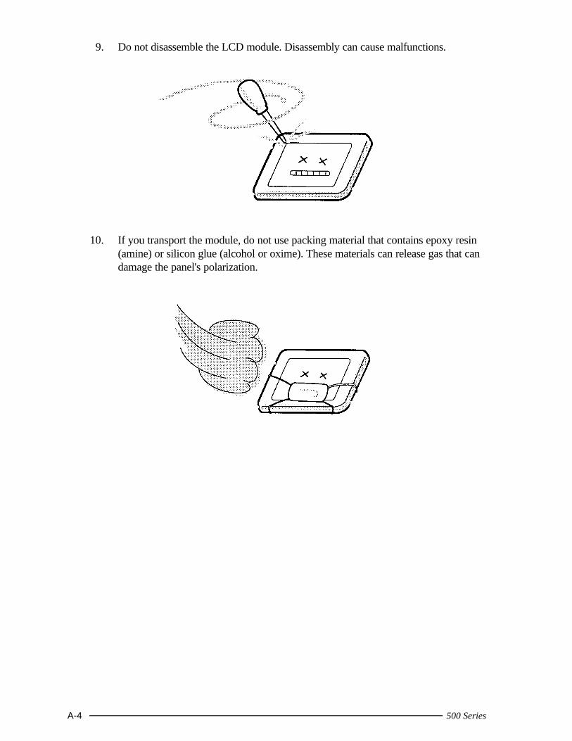
A-4 500 Series
9. Do not disassemble the LCD module. Disassembly can cause malfunctions.
10. If you transport the module, do not use packing material that contains epoxy resin(amine) or silicon glue (alcohol or oxime). These materials can release gas that candamage the panel's polarization.
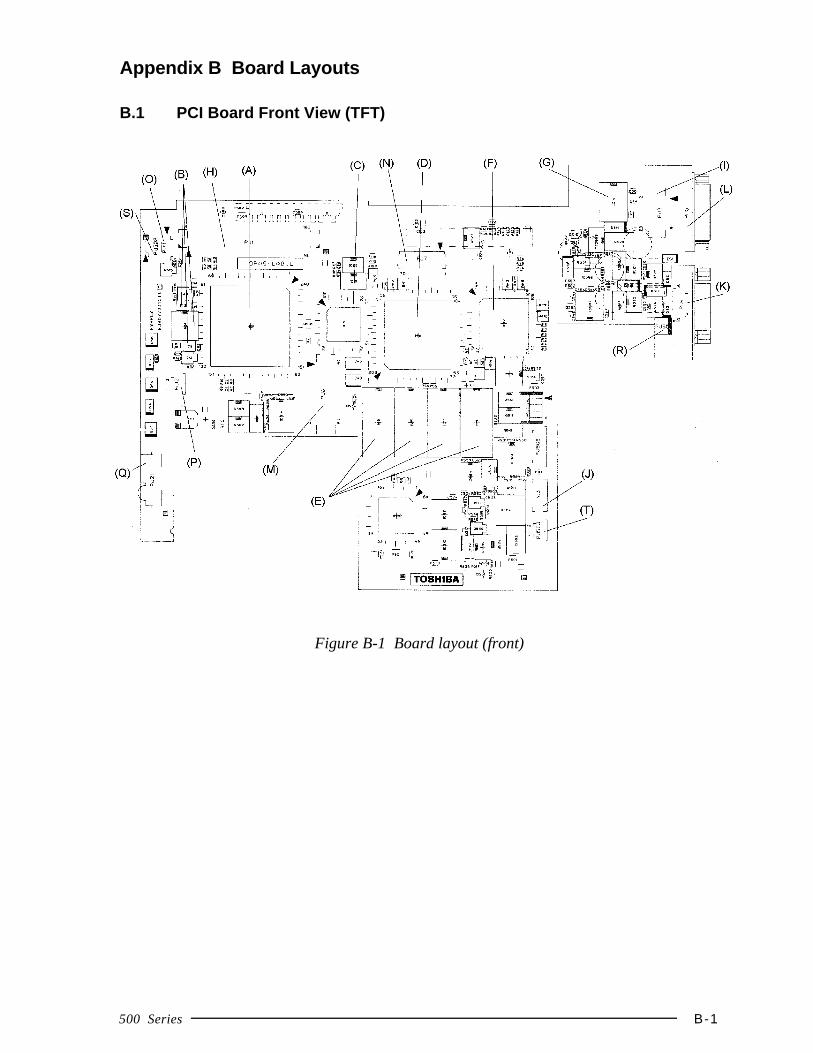
500 Series B-1
Appendix B Board Layouts
B.1 PCI Board Front View (TFT)
Figure B-1 Board layout (front)
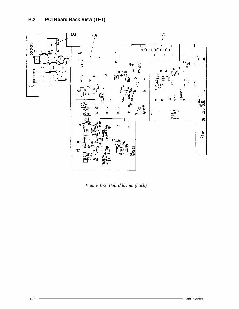
B-2 500 Series
B.2 PCI Board Back View (TFT)
Figure B-2 Board layout (back)
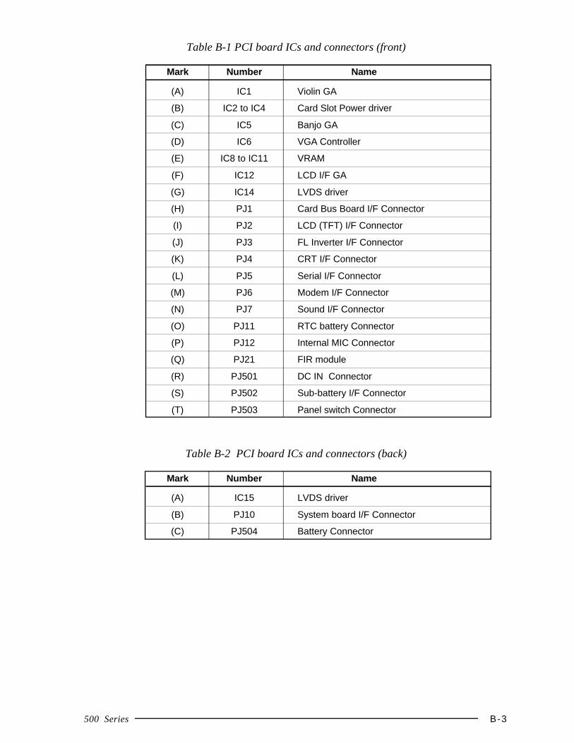
500 Series B-3
Table B-1 PCI board ICs and connectors (front)
Mark Number Name
(A) IC1 Violin GA
(B) IC2 to IC4 Card Slot Power driver
(C) IC5 Banjo GA
(D) IC6 VGA Controller
(E) IC8 to IC11 VRAM
(F) IC12 LCD I/F GA
(G) IC14 LVDS driver
(H) PJ1 Card Bus Board I/F Connector
(I) PJ2 LCD (TFT) I/F Connector
(J) PJ3 FL Inverter I/F Connector
(K) PJ4 CRT I/F Connector
(L) PJ5 Serial I/F Connector
(M) PJ6 Modem I/F Connector
(N) PJ7 Sound I/F Connector
(O) PJ11 RTC battery Connector
(P) PJ12 Internal MIC Connector
(Q) PJ21 FIR module
(R) PJ501 DC IN Connector
(S) PJ502 Sub-battery I/F Connector
(T) PJ503 Panel switch Connector
Table B-2 PCI board ICs and connectors (back)
Mark Number Name
(A) IC15 LVDS driver
(B) PJ10 System board I/F Connector
(C) PJ504 Battery Connector
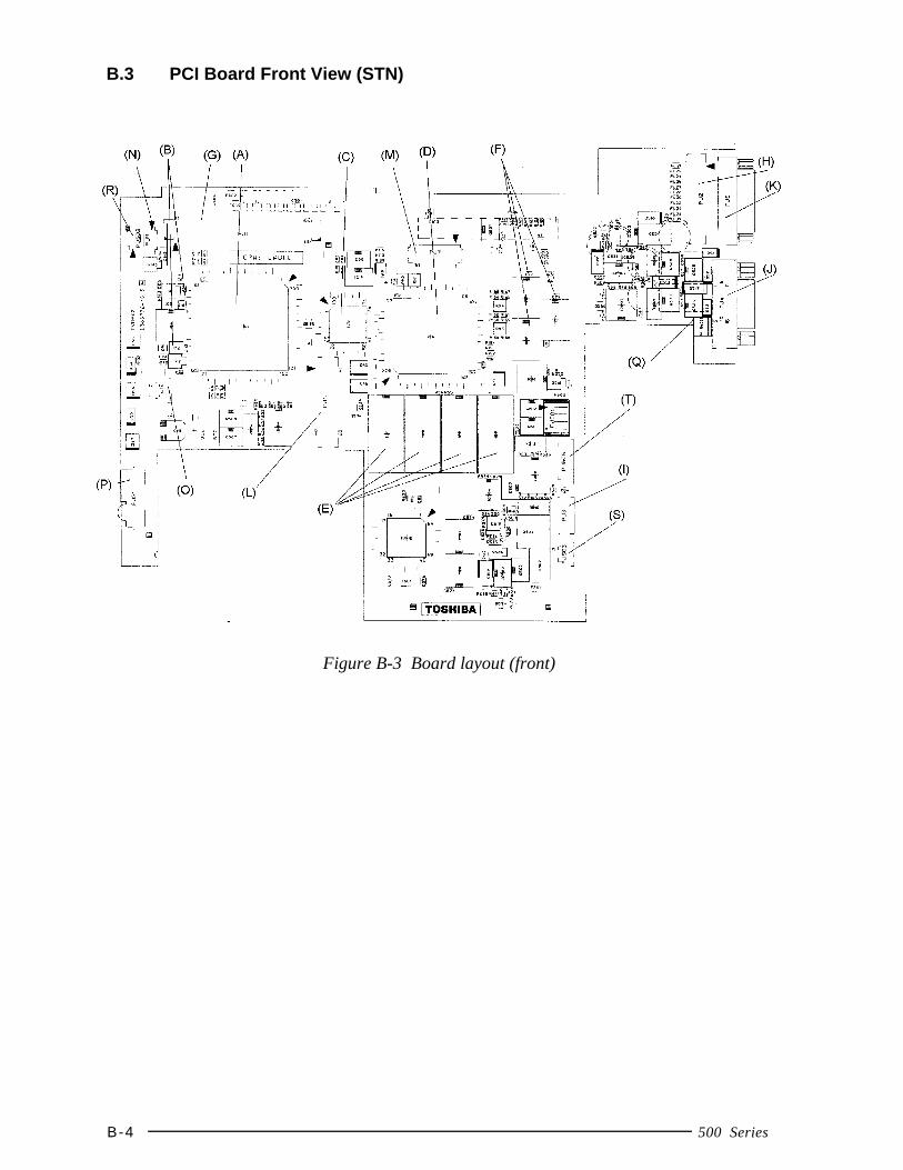
B-4 500 Series
B.3 PCI Board Front View (STN)
Figure B-3 Board layout (front)
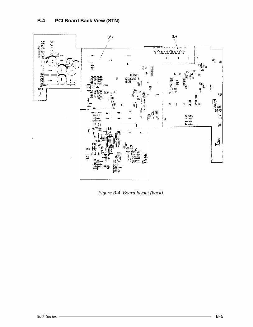
500 Series B-5
B.4 PCI Board Back View (STN)
Figure B-4 Board layout (back)
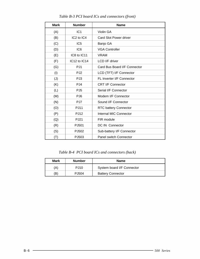
B-6 500 Series
Table B-3 PCI board ICs and connectors (front)
Mark Number Name
(A) IC1 Violin GA
(B) IC2 to IC4 Card Slot Power driver
(C) IC5 Banjo GA
(D) IC6 VGA Controller
(E) IC8 to IC11 VRAM
(F) IC12 to IC14 LCD I/F driver
(G) PJ1 Card Bus Board I/F Connector
(I) PJ2 LCD (TFT) I/F Connector
(J) PJ3 FL Inverter I/F Connector
(K) PJ4 CRT I/F Connector
(L) PJ5 Serial I/F Connector
(M) PJ6 Modem I/F Connector
(N) PJ7 Sound I/F Connector
(O) PJ11 RTC battery Connector
(P) PJ12 Internal MIC Connector
(Q) PJ21 FIR module
(R) PJ501 DC IN Connector
(S) PJ502 Sub-battery I/F Connector
(T) PJ503 Panel switch Connector
Table B-4 PCI board ICs and connectors (back)
Mark Number Name
(A) PJ10 System board I/F Connector
(B) PJ504 Battery Connector
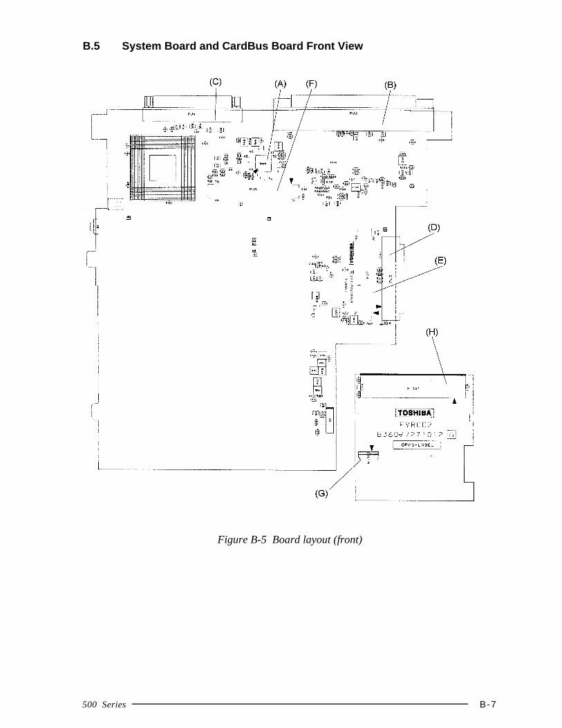
500 Series B-7
B.5 System Board and CardBus Board Front View
Figure B-5 Board layout (front)
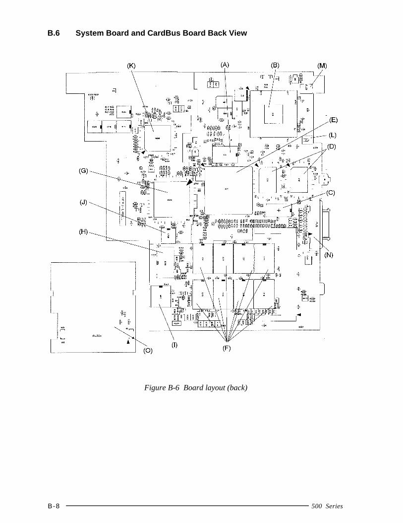
B-8 500 Series
B.6 System Board and CardBus Board Back View
Figure B-6 Board layout (back)
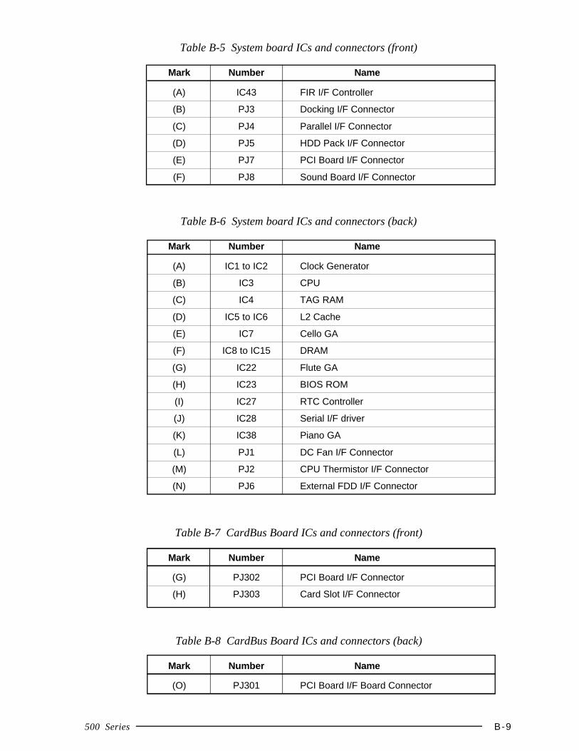
500 Series B-9
Table B-5 System board ICs and connectors (front)
Mark Number Name
(A) IC43 FIR I/F Controller
(B) PJ3 Docking I/F Connector
(C) PJ4 Parallel I/F Connector
(D) PJ5 HDD Pack I/F Connector
(E) PJ7 PCI Board I/F Connector
(F) PJ8 Sound Board I/F Connector
Table B-6 System board ICs and connectors (back)
Mark Number Name
(A) IC1 to IC2 Clock Generator
(B) IC3 CPU
(C) IC4 TAG RAM
(D) IC5 to IC6 L2 Cache
(E) IC7 Cello GA
(F) IC8 to IC15 DRAM
(G) IC22 Flute GA
(H) IC23 BIOS ROM
(I) IC27 RTC Controller
(J) IC28 Serial I/F driver
(K) IC38 Piano GA
(L) PJ1 DC Fan I/F Connector
(M) PJ2 CPU Thermistor I/F Connector
(N) PJ6 External FDD I/F Connector
Table B-7 CardBus Board ICs and connectors (front)
Mark Number Name
(G) PJ302 PCI Board I/F Connector
(H) PJ303 Card Slot I/F Connector
Table B-8 CardBus Board ICs and connectors (back)
Mark Number Name
(O) PJ301 PCI Board I/F Board Connector
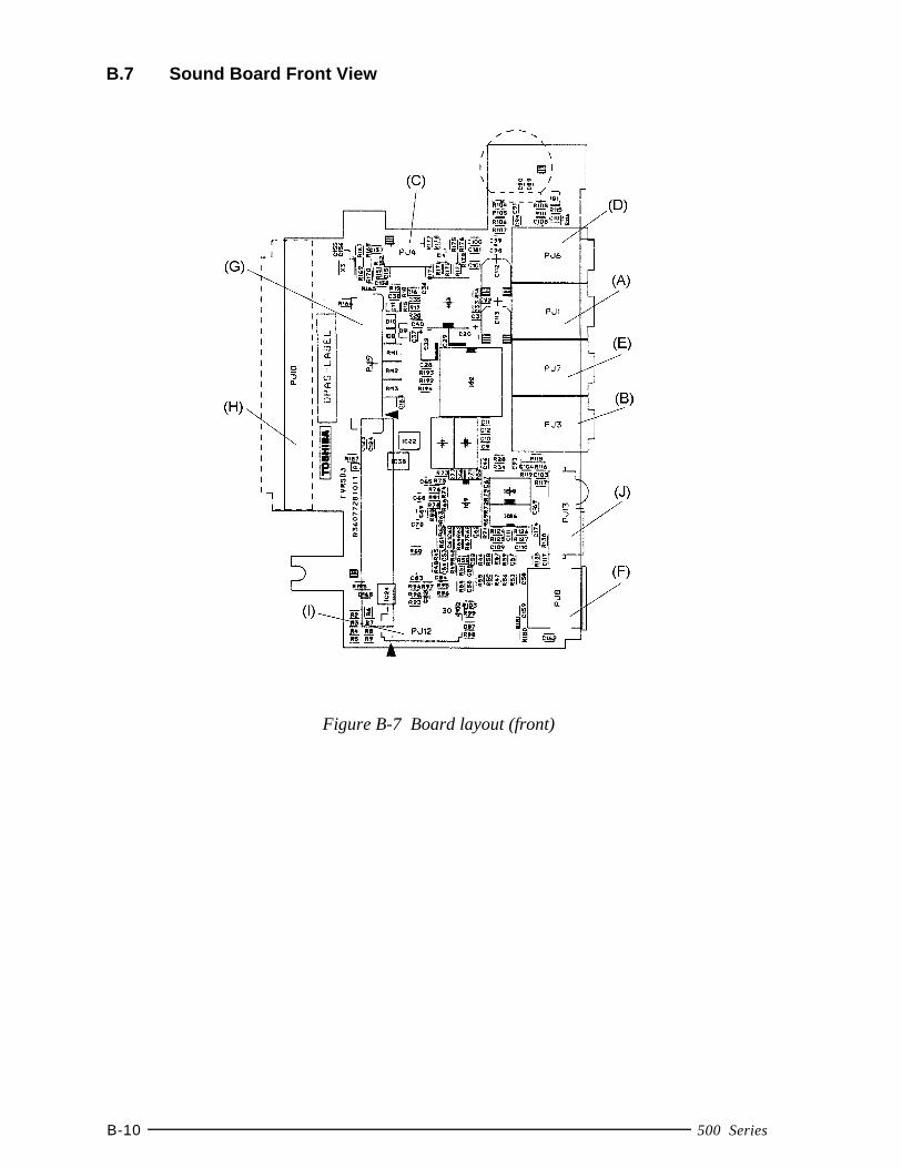
B-10 500 Series
B.7 Sound Board Front View
Figure B-7 Board layout (front)
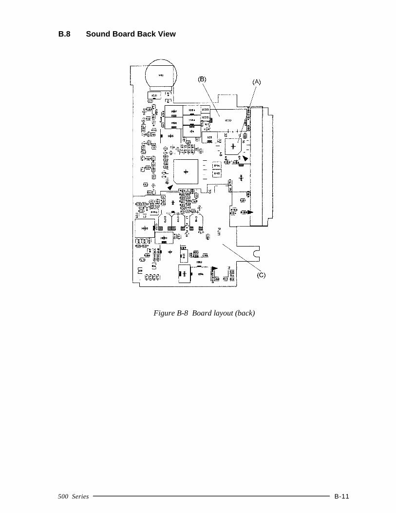
500 Series B-11
B.8 Sound Board Back View
Figure B-8 Board layout (back)
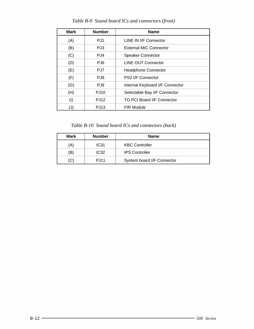
B-12 500 Series
Table B-9 Sound board ICs and connectors (front)
Mark Number Name
(A) PJ1 LINE IN I/F Connector
(B) PJ3 External MIC Connector
(C) PJ4 Speaker Connector
(D) PJ6 LINE OUT Connector
(E) PJ7 Headphone Connector
(F) PJ8 PS2 I/F Connector
(G) PJ9 Internal Keyboard I/F Connector
(H) PJ10 Selectable Bay I/F Connector
(I) PJ12 TO PCI Board I/F Connector
(J) PJ13 FIR Module
Table B-10 Sound board ICs and connectors (back)
Mark Number Name
(A) IC31 KBC Controller
(B) IC32 IPS Controller
(C) PJ11 System board I/F Connector
500 Series C-1
Appendix C Pin Assignments
C.1 PJ1 DC Fan I/F Connector (2-pin) on the System Board
Table C-1 PJ1 DC fan I/F connector pin assignments (2-pin)Pin No. Signal Name I/O Pin No. Signal Name I/O
1 FANPON - 2 GND -
C.2 PJ2 CPU Thermistor I/F Connector (3-pin) on the System Board
Table C-2 PJ2 CPU thermistor I/F connector pin assignments (3-pin)Pin No. Signal Name I/O Pin No. Signal Name I/O
1 CPUTMP;100 I 2 NC -
3 GND -
C.3 Expansion Memory Connector (144-pin) on the System Board
Table C-3 Expansion memory connector pin assignments (144-pin)Pin No. Signal Name I/O Pin No. Signal Name I/O
1 GND - 2 MD0;100 I/O
3 MD1;100 I/O 4 MD2;100 I/O
5 MD3;100 I/O 6 B3VDRM -
7 MD4;100 I/O 8 MD5;100 I/O
9 MD6;100 I/O 10 MD7;100 I/O
11 GND - 12 CAS0;002 O
13 CAS1;002 O 14 B3VDRM -
15 MA08;101 O 16 MA18;101 O
17 MA2;102 O 18 GND -
19 MD8;100 I/O 20 MD9;100 I/O
21 MD10;100 I/O 22 MD11;100 I/O
23 B3VDRM - 24 MD12;100 I/O
25 MD13;100 I/O 26 MD14;100 I/O
27 MD15;100 I/O 28 GND -
29 NC - 30 NC -
31 NC - 32 B3VDRM -
33 NC - 34 WEC;001 O
C-2 500 Series
Table C-3 Expansion memory connector pin assignments (144-pin)(continued)Pin No. Signal Name I/O Pin No. Signal Name I/O
35 RAS2;001 O 36 RAS3;001 O
37 B3VDRM - 38 B3VDRM -
39 NC - 40 NC -
41 B3VDRM - 42 MD16;100 I/O
43 MD17;100 I/O 44 MD18;100 I/O
45 MD19;100 I/O 46 GND -
47 MD20;100 I/O 48 MD21;100 I/O
49 MD22;100 I/O 50 MD23;100 I/O
51 B3VDRM - 52 MA6;102 O
53 MA8;102 O 54 GND -
55 MA9;102 O 56 MA10;102 O
57 B3VDRM - 58 CAS2;002 O
59 CAS3;002 O 60 GND -
61 MD24;100 I/O 62 MD25;100 I/O
63 MD26;100 I/O 64 MD27;100 I/O
65 B3VDRM - 66 MD28;100 I/O
67 MD29;100 I/O 68 MD30;100 I/O
69 MD31;100 I/O 70 GND -
71 NC - 72 B3VDRM -
73 GND - 74 MD32;100 I/O
75 MD33;100 I/O 76 MD34;100 I/O
77 MD35;100 I/O 78 B3VDRM -
79 MD36;100 I/O 80 MD37;100 I/O
81 MD38;100 I/O 82 MD39;100 I/O
83 GND - 84 CAS4;002 O
85 CAS5;002 O 86 B3VDRM -
87 MA3;102 O 88 MA4;102 O
89 MA5;102 O 90 GND -
91 MD40;100 I/O 92 MD41;100 I/O
93 MD42;100 I/O 94 MD43;100 I/O
95 B3VDRM - 96 MD44;100 I/O
97 MD45;100 I/O 98 MD46;100 I/O
99 MD47;100 I/O 100 GND -
101 NC - 102 NC -
103 NC - 104 B3VDRM -
105 WED;001 O 106 RAS4;001 O
107 RAS5;001 O 108 RAS6;001 O
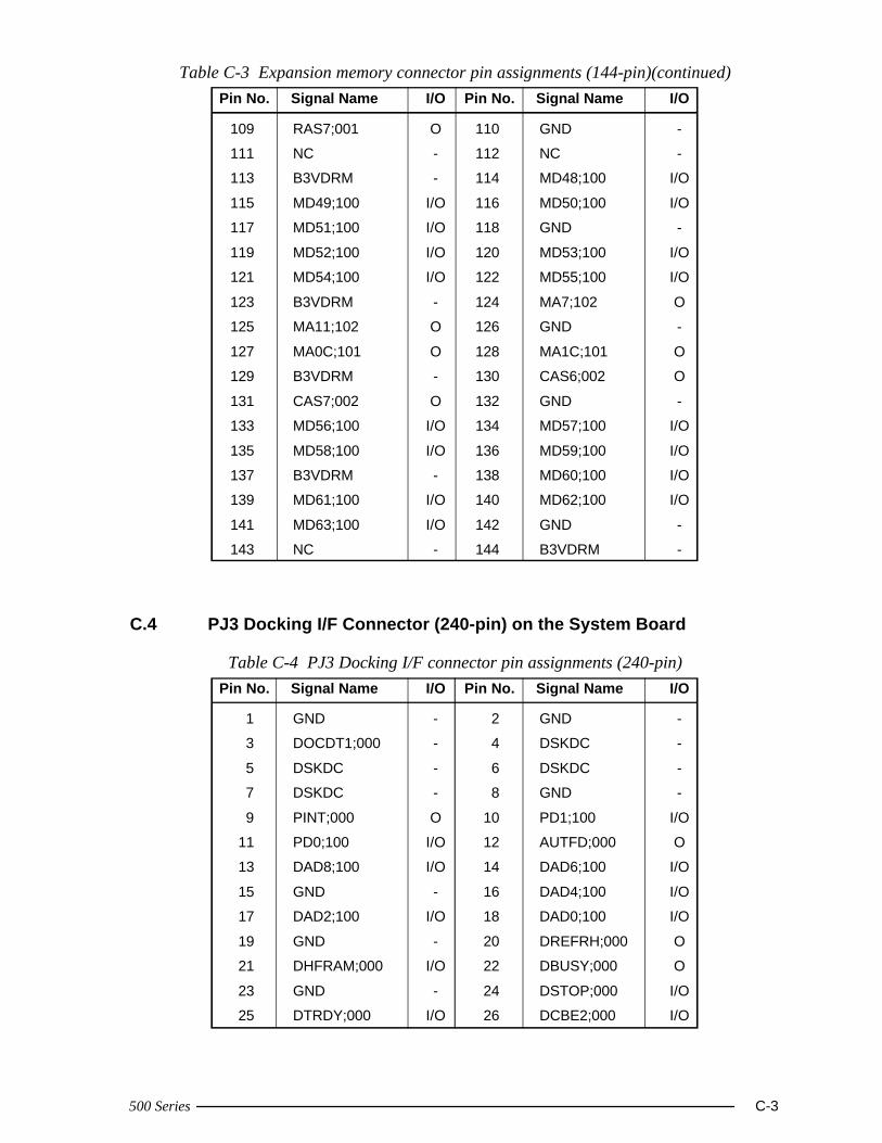
500 Series C-3
Table C-3 Expansion memory connector pin assignments (144-pin)(continued)Pin No. Signal Name I/O Pin No. Signal Name I/O
109 RAS7;001 O 110 GND -
111 NC - 112 NC -
113 B3VDRM - 114 MD48;100 I/O
115 MD49;100 I/O 116 MD50;100 I/O
117 MD51;100 I/O 118 GND -
119 MD52;100 I/O 120 MD53;100 I/O
121 MD54;100 I/O 122 MD55;100 I/O
123 B3VDRM - 124 MA7;102 O
125 MA11;102 O 126 GND -
127 MA0C;101 O 128 MA1C;101 O
129 B3VDRM - 130 CAS6;002 O
131 CAS7;002 O 132 GND -
133 MD56;100 I/O 134 MD57;100 I/O
135 MD58;100 I/O 136 MD59;100 I/O
137 B3VDRM - 138 MD60;100 I/O
139 MD61;100 I/O 140 MD62;100 I/O
141 MD63;100 I/O 142 GND -
143 NC - 144 B3VDRM -
C.4 PJ3 Docking I/F Connector (240-pin) on the System Board
Table C-4 PJ3 Docking I/F connector pin assignments (240-pin)Pin No. Signal Name I/O Pin No. Signal Name I/O
1 GND - 2 GND -
3 DOCDT1;000 - 4 DSKDC -
5 DSKDC - 6 DSKDC -
7 DSKDC - 8 GND -
9 PINT;000 O 10 PD1;100 I/O
11 PD0;100 I/O 12 AUTFD;000 O
13 DAD8;100 I/O 14 DAD6;100 I/O
15 GND - 16 DAD4;100 I/O
17 DAD2;100 I/O 18 DAD0;100 I/O
19 GND - 20 DREFRH;000 O
21 DHFRAM;000 I/O 22 DBUSY;000 O
23 GND - 24 DSTOP;000 I/O
25 DTRDY;000 I/O 26 DCBE2;000 I/O
C-4 500 Series
Table C-4 PJ3 Docking I/F connector pin assignments (240-pin)(continued)Pin No. Signal Name I/O Pin No. Signal Name I/O
27 GND - 28 DCBE0;000 I/O
29 DIOCHK;000 O 30 DSERR O
31 GND - 32 DINTC;000 I
33 GND - 34 DINTB;000 I
35 GND - 36 DINTA;000 I
37 DPREQ;000 I 38 DPGNT;000 O
39 MIDIIN;100 I 40 MIDIOT;100 O
41 VCC - 42 VCC -
43 VCC - 44 VCC -
45 SNDMUT;010 O 46 SPKDIS;100 O
47 MIKDIS;100 I 48 LINEIR;100 I
49 LINEIR;000 I 50 CDR;000 I
51 CDR;100 I 52 CDL;100 I
53 MIKR;000 I 54 MIKR;100 I
55 MIKL;000 I 56 LINEOR;100 O
57 LINEOL;000 O 58 LINEOR;000 O
59 LINEOL;100 O 60 MIKL;100 I
61 GND - 62 GND -
63 GND - 64 DSKDC -
65 DSKDC - 66 DSKDC -
67 PD3;100 I/O 68 GND -
69 PD4;100 I/O 70 ERROR;000 I
71 ACK;000 I 72 STROB;000 O
73 DAD7;100 I/O 74 DAD5;100 I/O
75 GND - 76 DAD3;100 I/O
77 DAD1;100 I/O 78 RCLR;100 I/O
79 GND - 80 DDEVSL;000 I/O
81 DPAR;100 I/O 82 DPERR I
83 GND - 84 DIRDY;000 I/O
85 DCBE3;000 I/O 86 DCBE1;000 I/O
87 GND - 88 DIRQCK;100 O
89 DIRQDT;000 I/O 90 DINTD;000 I
91 GND - 92 GND -
93 GND - 94 DGNT;000 O
95 GND - 96 GND -
97 DFRAME;000 I/O 98 NC -
99 IFLD2A;000 O 100 EXKBCK;100 I/O
500 Series C-5
Table C-4 PJ3 Docking I/F connector pin assignments (240-pin)(continued)Pin No. Signal Name I/O Pin No. Signal Name I/O
101 NC - 102 EXKBDT;100 I/O
103 GND - 104 MOUSCK;100 I/O
105 QSWON;100 O 106 MOUSDT;100 I/O
107 PCM2SP;100 I 108 LINEIL;000 I
109 GND - 110 LINEIL;100 I
111 DOCSMI;100 I 112 CDL;000 I
113 EJCTRQ;100 I 114 JOYDTO;100 I
115 GND - 116 JOYDT2;100 I
117 JOYDT3;100 I 118 JOYDT5;100 I
119 GND - 120 JOYDT7;100 I
121 GND - 122 GND -
123 NC - 124 GND -
125 NC - 126 DSKDC -
127 PD5;100 I/O 128 SLIN;000 O
129 PD6;100 I/O 130 GND -
131 MCV - 132 PE;100 I
133 DAD31;100 I/O 134 DAD17;100 I/O
135 GND - 136 DAD16;100 I/O
137 DAD28;100 I/O 138 DAD15;100 I/O
139 GND - 140 DAD14;100 I/O
141 DAD25;100 I/O 142 DAD13;100 I/O
143 GND - 144 DAD12;100 I/O
145 DAD22;100 I/O 146 DAD11;100 I/O
147 GND - 148 DAD10;100 I/O
149 DAD19;100 I/O 150 DAD9;100 I/O
151 GND - 152 GND -
153 GND - 154 DREQ;000 I
155 GND - 156 GND -
157 NC - 158 NC -
159 DCD1;100 I 160 SCL;100 I/O
161 RXD1;000 I 162 SDA;100 I/O
163 GND - 164 DCRIOT;100 I
165 CTS1;100 I 166 DSCREQ;000 I
167 GND - 168 DSCGNT;000 O
169 DTR1;110 O 170 DCPCLR;010 O
171 MONID0;100 I/O 172 GND -
173 MONID1;100 I/O 174 DSKCHG;000 I
C-6 500 Series
Table C-4 PJ3 Docking I/F connector pin assignments (240-pin)(continued)Pin No. Signal Name I/O Pin No. Signal Name I/O
175 MONID2;100 I/O 176 JOYDT1;100 I
177 MONID3;100 I/O 178 JOYDT4;100 I
179 NC - 180 JOYDT6;100 I
181 GND - 182 SELCT;100 I
183 GND - 184 BUSY;100 I
185 GND - 186 PD7;100 I/O
187 GND - 188 PD2;100 I/O
189 GND - 190 PCONF;100 I
191 GND - 192 DOCPWR;100 O
193 GND - 194 DAD30;100 I/O
195 GND - 196 DAD29;100 I/O
197 GND - 198 DAD27;100 I/O
199 GND - 200 DAD26;100 I/O
201 GND - 202 DAD24;100 I/O
203 GND - 204 DAD23;100 I/O
205 GND - 206 DAD21;100 I/O
207 GND - 208 DAD20;100 I/O
209 GND - 210 DAD18;100 I/O
211 GND - 212 GND -
213 GND - 214 DSCLK;100 O
215 GND - 216 GND -
217 GND - 218 RI1;100 I
219 GND - 220 DSR1;100 I
221 GND - 222 RTS1;110 O
223 GND - 224 TXD1;010 O
225 GND - 226 SIRRXP;100 I
227 GND - 228 FIRTXB;100 O
229 GND - 230 CHSYNC;100 O
231 GND - 232 CVSYNC;100 O
233 GND - 234 CRED;100 O
235 GND - 236 CGREEN;100 O
237 GND - 238 CBLUE;100 O
239 GND - 240 DOCDT2;000 I
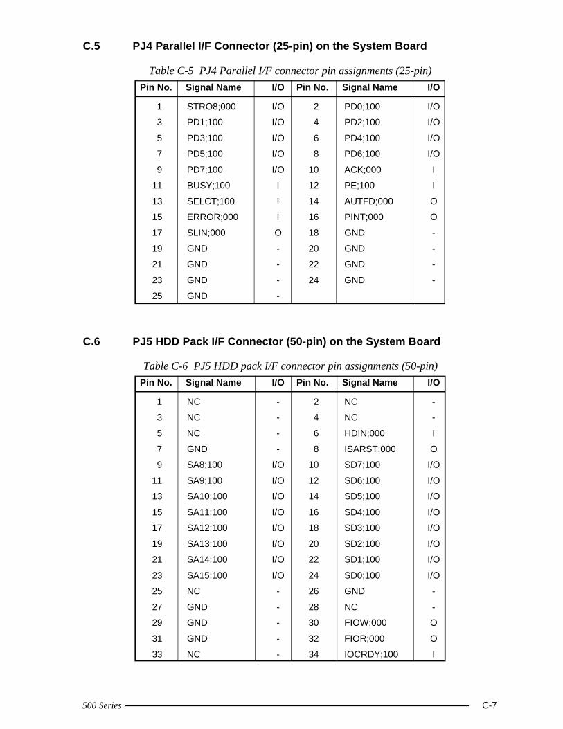
500 Series C-7
C.5 PJ4 Parallel I/F Connector (25-pin) on the System Board
Table C-5 PJ4 Parallel I/F connector pin assignments (25-pin)Pin No. Signal Name I/O Pin No. Signal Name I/O
1 STRO8;000 I/O 2 PD0;100 I/O
3 PD1;100 I/O 4 PD2;100 I/O
5 PD3;100 I/O 6 PD4;100 I/O
7 PD5;100 I/O 8 PD6;100 I/O
9 PD7;100 I/O 10 ACK;000 I
11 BUSY;100 I 12 PE;100 I
13 SELCT;100 I 14 AUTFD;000 O
15 ERROR;000 I 16 PINT;000 O
17 SLIN;000 O 18 GND -
19 GND - 20 GND -
21 GND - 22 GND -
23 GND - 24 GND -
25 GND -
C.6 PJ5 HDD Pack I/F Connector (50-pin) on the System Board
Table C-6 PJ5 HDD pack I/F connector pin assignments (50-pin)Pin No. Signal Name I/O Pin No. Signal Name I/O
1 NC - 2 NC -
3 NC - 4 NC -
5 NC - 6 HDIN;000 I
7 GND - 8 ISARST;000 O
9 SA8;100 I/O 10 SD7;100 I/O
11 SA9;100 I/O 12 SD6;100 I/O
13 SA10;100 I/O 14 SD5;100 I/O
15 SA11;100 I/O 16 SD4;100 I/O
17 SA12;100 I/O 18 SD3;100 I/O
19 SA13;100 I/O 20 SD2;100 I/O
21 SA14;100 I/O 22 SD1;100 I/O
23 SA15;100 I/O 24 SD0;100 I/O
25 NC - 26 GND -
27 GND - 28 NC -
29 GND - 30 FIOW;000 O
31 GND - 32 FIOR;000 O
33 NC - 34 IOCRDY;100 I
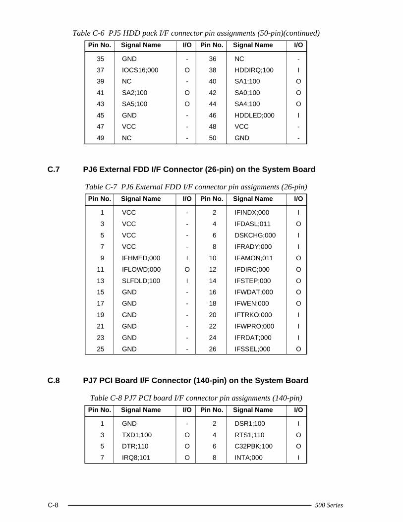
C-8 500 Series
Table C-6 PJ5 HDD pack I/F connector pin assignments (50-pin)(continued)Pin No. Signal Name I/O Pin No. Signal Name I/O
35 GND - 36 NC -
37 IOCS16;000 O 38 HDDIRQ;100 I
39 NC - 40 SA1;100 O
41 SA2;100 O 42 SA0;100 O
43 SA5;100 O 44 SA4;100 O
45 GND - 46 HDDLED;000 I
47 VCC - 48 VCC -
49 NC - 50 GND -
C.7 PJ6 External FDD I/F Connector (26-pin) on the System Board
Table C-7 PJ6 External FDD I/F connector pin assignments (26-pin)Pin No. Signal Name I/O Pin No. Signal Name I/O
1 VCC - 2 IFINDX;000 I
3 VCC - 4 IFDASL;011 O
5 VCC - 6 DSKCHG;000 I
7 VCC - 8 IFRADY;000 I
9 IFHMED;000 I 10 IFAMON;011 O
11 IFLOWD;000 O 12 IFDIRC;000 O
13 SLFDLD;100 I 14 IFSTEP;000 O
15 GND - 16 IFWDAT;000 O
17 GND - 18 IFWEN;000 O
19 GND - 20 IFTRKO;000 I
21 GND - 22 IFWPRO;000 I
23 GND - 24 IFRDAT;000 I
25 GND - 26 IFSSEL;000 O
C.8 PJ7 PCI Board I/F Connector (140-pin) on the System Board
Table C-8 PJ7 PCI board I/F connector pin assignments (140-pin)Pin No. Signal Name I/O Pin No. Signal Name I/O
1 GND - 2 DSR1;100 I
3 TXD1;100 O 4 RTS1;110 O
5 DTR;110 O 6 C32PBK;100 O
7 IRQ8;101 O 8 INTA;000 I
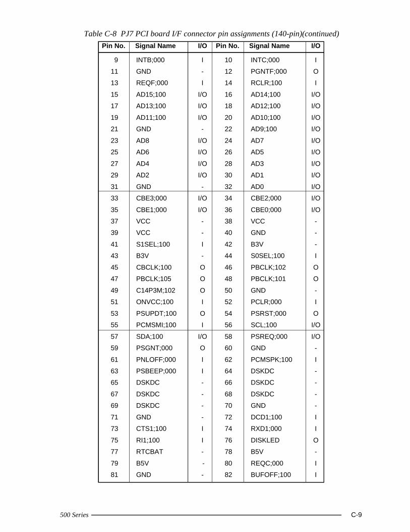
500 Series C-9
Table C-8 PJ7 PCI board I/F connector pin assignments (140-pin)(continued)Pin No. Signal Name I/O Pin No. Signal Name I/O
9 INTB;000 I 10 INTC;000 I
11 GND - 12 PGNTF;000 O
13 REQF;000 I 14 RCLR;100 I
15 AD15;100 I/O 16 AD14;100 I/O
17 AD13;100 I/O 18 AD12;100 I/O
19 AD11;100 I/O 20 AD10;100 I/O
21 GND - 22 AD9;100 I/O
23 AD8 I/O 24 AD7 I/O
25 AD6 I/O 26 AD5 I/O
27 AD4 I/O 28 AD3 I/O
29 AD2 I/O 30 AD1 I/O
31 GND - 32 AD0 I/O
33 CBE3;000 I/O 34 CBE2;000 I/O
35 CBE1;000 I/O 36 CBE0;000 I/O
37 VCC - 38 VCC -
39 VCC - 40 GND -
41 S1SEL;100 I 42 B3V -
43 B3V - 44 S0SEL;100 I
45 CBCLK;100 O 46 PBCLK;102 O
47 PBCLK;105 O 48 PBCLK;101 O
49 C14P3M;102 O 50 GND -
51 ONVCC;100 I 52 PCLR;000 I
53 PSUPDT;100 O 54 PSRST;000 O
55 PCMSMI;100 I 56 SCL;100 I/O
57 SDA;100 I/O 58 PSREQ;000 I/O
59 PSGNT;000 O 60 GND -
61 PNLOFF;000 I 62 PCMSPK;100 I
63 PSBEEP;000 I 64 DSKDC -
65 DSKDC - 66 DSKDC -
67 DSKDC - 68 DSKDC -
69 DSKDC - 70 GND -
71 GND - 72 DCD1;100 I
73 CTS1;100 I 74 RXD1;000 I
75 RI1;100 I 76 DISKLED O
77 RTCBAT - 78 B5V -
79 B5V - 80 REQC;000 I
81 GND - 82 BUFOFF;100 I
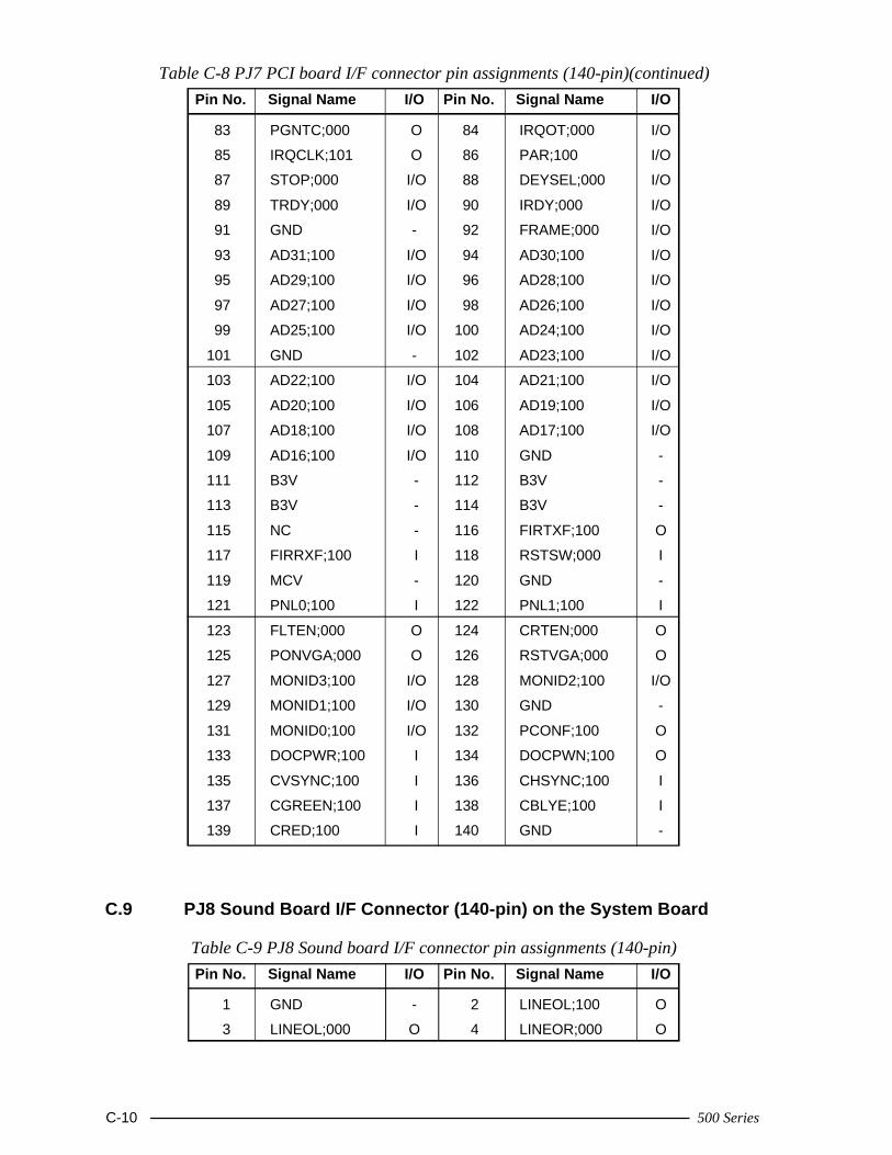
C-10 500 Series
Table C-8 PJ7 PCI board I/F connector pin assignments (140-pin)(continued)Pin No. Signal Name I/O Pin No. Signal Name I/O
83 PGNTC;000 O 84 IRQOT;000 I/O
85 IRQCLK;101 O 86 PAR;100 I/O
87 STOP;000 I/O 88 DEYSEL;000 I/O
89 TRDY;000 I/O 90 IRDY;000 I/O
91 GND - 92 FRAME;000 I/O
93 AD31;100 I/O 94 AD30;100 I/O
95 AD29;100 I/O 96 AD28;100 I/O
97 AD27;100 I/O 98 AD26;100 I/O
99 AD25;100 I/O 100 AD24;100 I/O
101 GND - 102 AD23;100 I/O
103 AD22;100 I/O 104 AD21;100 I/O
105 AD20;100 I/O 106 AD19;100 I/O
107 AD18;100 I/O 108 AD17;100 I/O
109 AD16;100 I/O 110 GND -
111 B3V - 112 B3V -
113 B3V - 114 B3V -
115 NC - 116 FIRTXF;100 O
117 FIRRXF;100 I 118 RSTSW;000 I
119 MCV - 120 GND -
121 PNL0;100 I 122 PNL1;100 I
123 FLTEN;000 O 124 CRTEN;000 O
125 PONVGA;000 O 126 RSTVGA;000 O
127 MONID3;100 I/O 128 MONID2;100 I/O
129 MONID1;100 I/O 130 GND -
131 MONID0;100 I/O 132 PCONF;100 O
133 DOCPWR;100 I 134 DOCPWN;100 O
135 CVSYNC;100 I 136 CHSYNC;100 I
137 CGREEN;100 I 138 CBLYE;100 I
139 CRED;100 I 140 GND -
C.9 PJ8 Sound Board I/F Connector (140-pin) on the System Board
Table C-9 PJ8 Sound board I/F connector pin assignments (140-pin)Pin No. Signal Name I/O Pin No. Signal Name I/O
1 GND - 2 LINEOL;100 O
3 LINEOL;000 O 4 LINEOR;000 O
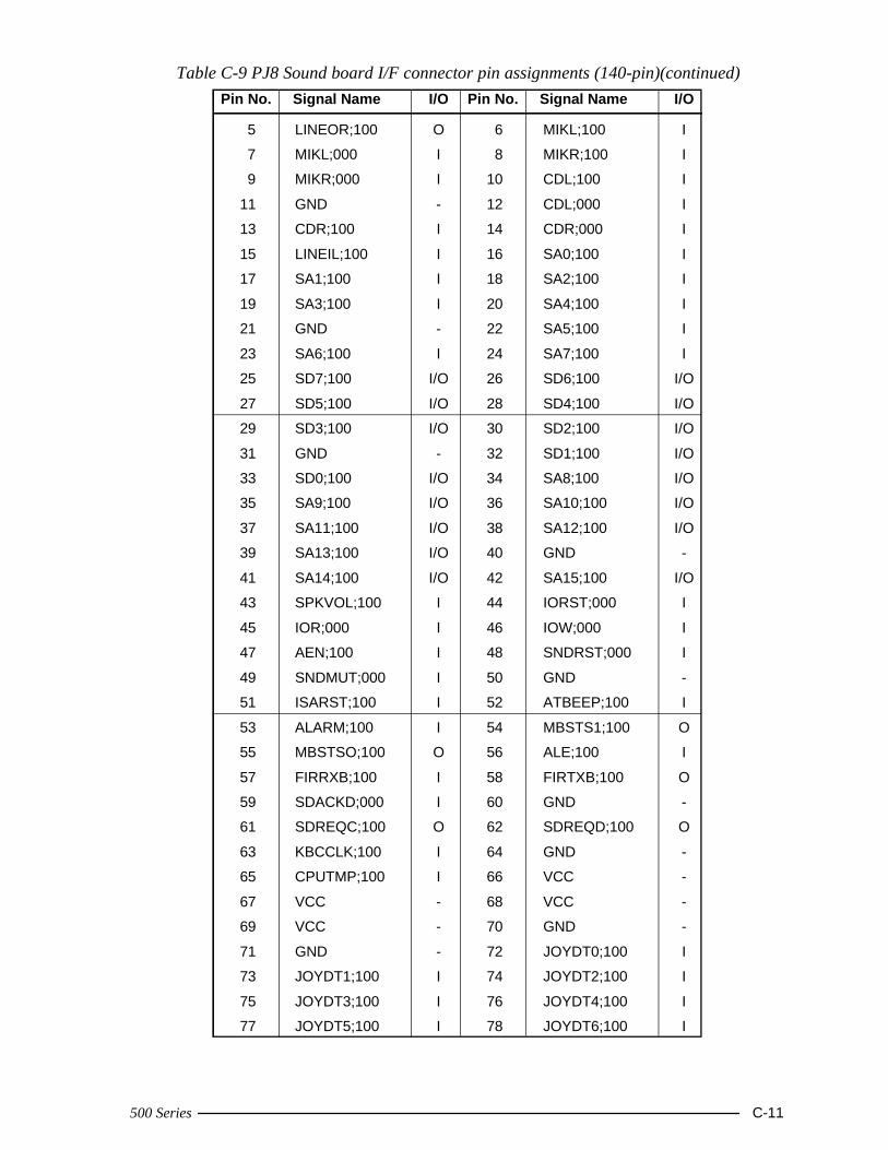
500 Series C-11
Table C-9 PJ8 Sound board I/F connector pin assignments (140-pin)(continued)Pin No. Signal Name I/O Pin No. Signal Name I/O
5 LINEOR;100 O 6 MIKL;100 I
7 MIKL;000 I 8 MIKR;100 I
9 MIKR;000 I 10 CDL;100 I
11 GND - 12 CDL;000 I
13 CDR;100 I 14 CDR;000 I
15 LINEIL;100 I 16 SA0;100 I
17 SA1;100 I 18 SA2;100 I
19 SA3;100 I 20 SA4;100 I
21 GND - 22 SA5;100 I
23 SA6;100 I 24 SA7;100 I
25 SD7;100 I/O 26 SD6;100 I/O
27 SD5;100 I/O 28 SD4;100 I/O
29 SD3;100 I/O 30 SD2;100 I/O
31 GND - 32 SD1;100 I/O
33 SD0;100 I/O 34 SA8;100 I/O
35 SA9;100 I/O 36 SA10;100 I/O
37 SA11;100 I/O 38 SA12;100 I/O
39 SA13;100 I/O 40 GND -
41 SA14;100 I/O 42 SA15;100 I/O
43 SPKVOL;100 I 44 IORST;000 I
45 IOR;000 I 46 IOW;000 I
47 AEN;100 I 48 SNDRST;000 I
49 SNDMUT;000 I 50 GND -
51 ISARST;100 I 52 ATBEEP;100 I
53 ALARM;100 I 54 MBSTS1;100 O
55 MBSTSO;100 O 56 ALE;100 I
57 FIRRXB;100 I 58 FIRTXB;100 O
59 SDACKD;000 I 60 GND -
61 SDREQC;100 O 62 SDREQD;100 O
63 KBCCLK;100 I 64 GND -
65 CPUTMP;100 I 66 VCC -
67 VCC - 68 VCC -
69 VCC - 70 GND -
71 GND - 72 JOYDT0;100 I
73 JOYDT1;100 I 74 JOYDT2;100 I
75 JOYDT3;100 I 76 JOYDT4;100 I
77 JOYDT5;100 I 78 JOYDT6;100 I
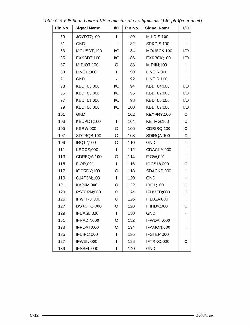
C-12 500 Series
Table C-9 PJ8 Sound board I/F connector pin assignments (140-pin)(continued)Pin No. Signal Name I/O Pin No. Signal Name I/O
79 JOYDT7;100 I 80 MIKDIS;100 I
81 GND - 82 SPKDIS;100 I
83 MOUSDT;100 I/O 84 MOUSCK;100 I/O
85 EXKBDT;100 I/O 86 EXKBCK;100 I/O
87 MIDIOT;100 O 88 MIDIIN;100 I
89 LINEIL;000 I 90 LINEIR;000 I
91 GND - 92 LINEIR;100 I
93 KBDT05;000 I/O 94 KBDT04;000 I/O
95 KBDT03;000 I/O 96 KBDT02;000 I/O
97 KBDT01;000 I/O 98 KBDT00;000 I/O
99 KBDT06;000 I/O 100 KBDT07;000 I/O
101 GND - 102 KEYPRS;100 O
103 KBUPDT;100 I 104 KBTMG;100 O
105 KBRW;000 O 106 CDRIRQ;100 O
107 SDTRQB;100 O 108 SDIRQA;100 O
109 IRQ12;100 O 110 GND -
111 KBCCS;000 I 112 CDACKA;000 I
113 CDREQA;100 O 114 FIOW;001 I
115 FIOR;001 I 116 IOCS16;000 O
117 IOCRDY;100 O 118 SDACKC;000 I
119 C14P3M;103 I 120 GND -
121 KA20M;000 O 122 IRQ1;100 O
123 RSTCPN;000 O 124 IFHMED;000 O
125 IFWPRD;000 O 126 IFLD2A;000 I
127 DSKCHG;000 O 128 IFINDX;000 O
129 IFDASL;000 I 130 GND -
131 IFRADY;000 O 132 IFWDAT;000 I
133 IFRDAT;000 O 134 IFAMON;000 I
135 IFDIRC;000 I 136 IFSTEP;000 I
137 IFWEN;000 I 138 IFTRKO;000 O
139 IFSSEL;000 I 140 GND -
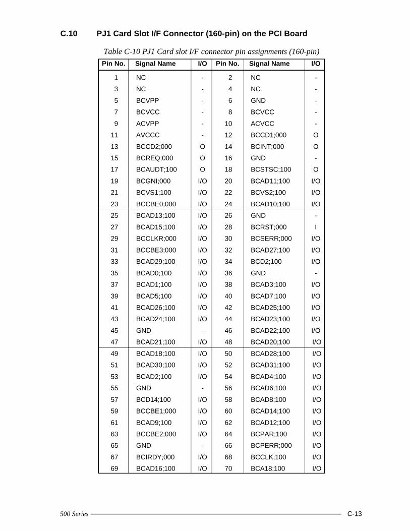
500 Series C-13
C.10 PJ1 Card Slot I/F Connector (160-pin) on the PCI Board
Table C-10 PJ1 Card slot I/F connector pin assignments (160-pin)Pin No. Signal Name I/O Pin No. Signal Name I/O
1 NC - 2 NC -
3 NC - 4 NC -
5 BCVPP - 6 GND -
7 BCVCC - 8 BCVCC -
9 ACVPP - 10 ACVCC -
11 AVCCC - 12 BCCD1;000 O
13 BCCD2;000 O 14 BCINT;000 O
15 BCREQ;000 O 16 GND -
17 BCAUDT;100 O 18 BCSTSC;100 O
19 BCGNI;000 I/O 20 BCAD11;100 I/O
21 BCVS1;100 I/O 22 BCVS2;100 I/O
23 BCCBE0;000 I/O 24 BCAD10;100 I/O
25 BCAD13;100 I/O 26 GND -
27 BCAD15;100 I/O 28 BCRST;000 I
29 BCCLKR;000 I/O 30 BCSERR;000 I/O
31 BCCBE3;000 I/O 32 BCAD27;100 I/O
33 BCAD29;100 I/O 34 BCD2;100 I/O
35 BCAD0;100 I/O 36 GND -
37 BCAD1;100 I/O 38 BCAD3;100 I/O
39 BCAD5;100 I/O 40 BCAD7;100 I/O
41 BCAD26;100 I/O 42 BCAD25;100 I/O
43 BCAD24;100 I/O 44 BCAD23;100 I/O
45 GND - 46 BCAD22;100 I/O
47 BCAD21;100 I/O 48 BCAD20;100 I/O
49 BCAD18;100 I/O 50 BCAD28;100 I/O
51 BCAD30;100 I/O 52 BCAD31;100 I/O
53 BCAD2;100 I/O 54 BCAD4;100 I/O
55 GND - 56 BCAD6;100 I/O
57 BCD14;100 I/O 58 BCAD8;100 I/O
59 BCCBE1;000 I/O 60 BCAD14;100 I/O
61 BCAD9;100 I/O 62 BCAD12;100 I/O
63 BCCBE2;000 I/O 64 BCPAR;100 I/O
65 GND - 66 BCPERR;000 I/O
67 BCIRDY;000 I/O 68 BCCLK;100 I/O
69 BCAD16;100 I/O 70 BCA18;100 I/O
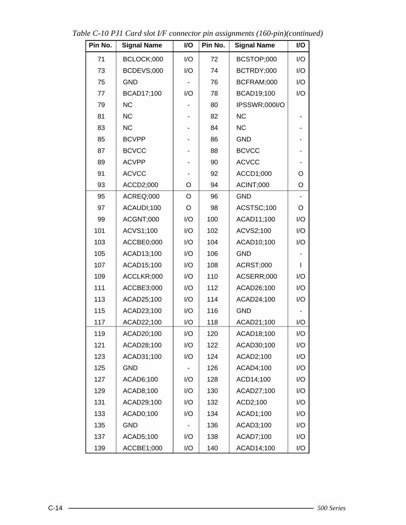
C-14 500 Series
Table C-10 PJ1 Card slot I/F connector pin assignments (160-pin)(continued)Pin No. Signal Name I/O Pin No. Signal Name I/O
71 BCLOCK;000 I/O 72 BCSTOP;000 I/O
73 BCDEVS;000 I/O 74 BCTRDY;000 I/O
75 GND - 76 BCFRAM;000 I/O
77 BCAD17;100 I/O 78 BCAD19;100 I/O
79 NC - 80 IPSSWR;000I/O
81 NC - 82 NC -
83 NC - 84 NC -
85 BCVPP - 86 GND -
87 BCVCC - 88 BCVCC -
89 ACVPP - 90 ACVCC -
91 ACVCC - 92 ACCD1;000 O
93 ACCD2;000 O 94 ACINT;000 O
95 ACREQ;000 O 96 GND -
97 ACAUDI;100 O 98 ACSTSC;100 O
99 ACGNT;000 I/O 100 ACAD11;100 I/O
101 ACVS1;100 I/O 102 ACVS2;100 I/O
103 ACCBE0;000 I/O 104 ACAD10;100 I/O
105 ACAD13;100 I/O 106 GND -
107 ACAD15;100 I/O 108 ACRST;000 I
109 ACCLKR;000 I/O 110 ACSERR;000 I/O
111 ACCBE3;000 I/O 112 ACAD26;100 I/O
113 ACAD25;100 I/O 114 ACAD24;100 I/O
115 ACAD23;100 I/O 116 GND -
117 ACAD22;100 I/O 118 ACAD21;100 I/O
119 ACAD20;100 I/O 120 ACAD18;100 I/O
121 ACAD28;100 I/O 122 ACAD30;100 I/O
123 ACAD31;100 I/O 124 ACAD2;100 I/O
125 GND - 126 ACAD4;100 I/O
127 ACAD6;100 I/O 128 ACD14;100 I/O
129 ACAD8;100 I/O 130 ACAD27;100 I/O
131 ACAD29;100 I/O 132 ACD2;100 I/O
133 ACAD0;100 I/O 134 ACAD1;100 I/O
135 GND - 136 ACAD3;100 I/O
137 ACAD5;100 I/O 138 ACAD7;100 I/O
139 ACCBE1;000 I/O 140 ACAD14;100 I/O
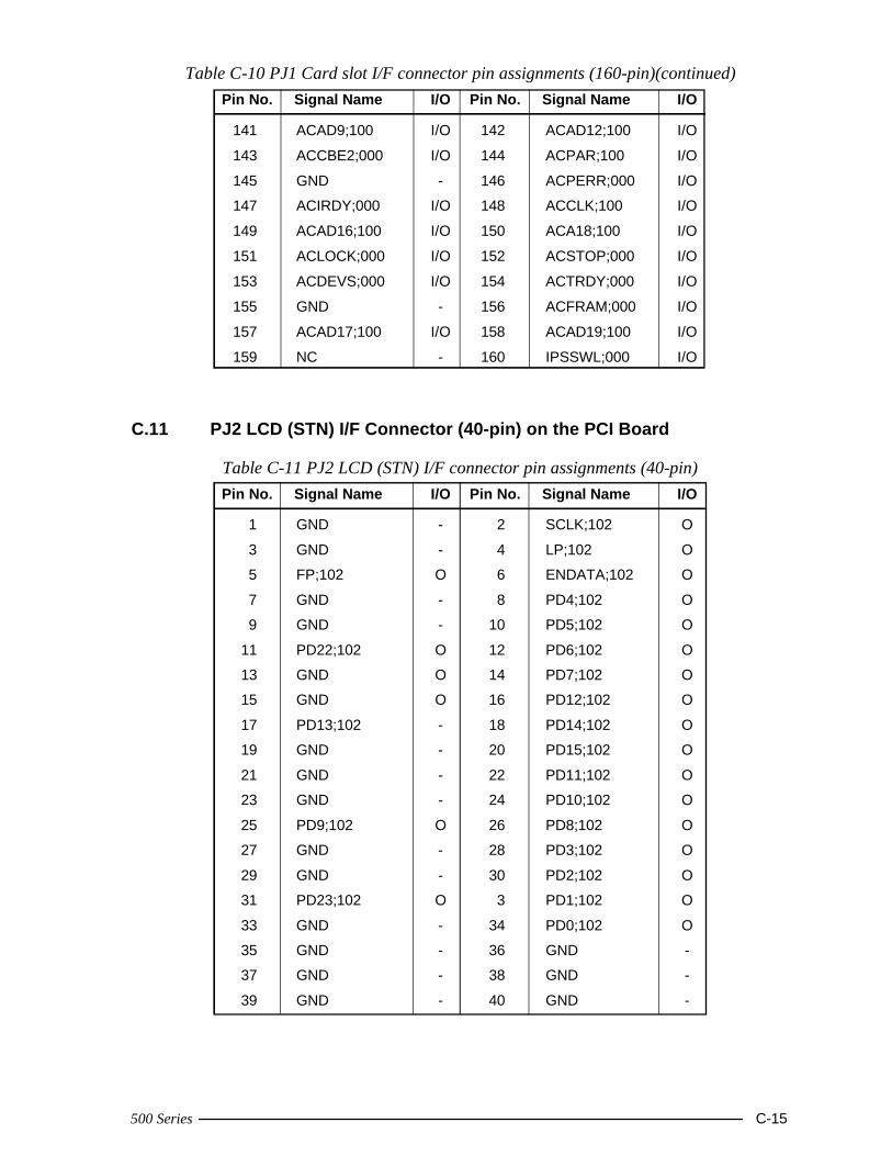
500 Series C-15
Table C-10 PJ1 Card slot I/F connector pin assignments (160-pin)(continued)Pin No. Signal Name I/O Pin No. Signal Name I/O
141 ACAD9;100 I/O 142 ACAD12;100 I/O
143 ACCBE2;000 I/O 144 ACPAR;100 I/O
145 GND - 146 ACPERR;000 I/O
147 ACIRDY;000 I/O 148 ACCLK;100 I/O
149 ACAD16;100 I/O 150 ACA18;100 I/O
151 ACLOCK;000 I/O 152 ACSTOP;000 I/O
153 ACDEVS;000 I/O 154 ACTRDY;000 I/O
155 GND - 156 ACFRAM;000 I/O
157 ACAD17;100 I/O 158 ACAD19;100 I/O
159 NC - 160 IPSSWL;000 I/O
C.11 PJ2 LCD (STN) I/F Connector (40-pin) on the PCI Board
Table C-11 PJ2 LCD (STN) I/F connector pin assignments (40-pin)Pin No. Signal Name I/O Pin No. Signal Name I/O
1 GND - 2 SCLK;102 O
3 GND - 4 LP;102 O
5 FP;102 O 6 ENDATA;102 O
7 GND - 8 PD4;102 O
9 GND - 10 PD5;102 O
11 PD22;102 O 12 PD6;102 O
13 GND O 14 PD7;102 O
15 GND O 16 PD12;102 O
17 PD13;102 - 18 PD14;102 O
19 GND - 20 PD15;102 O
21 GND - 22 PD11;102 O
23 GND - 24 PD10;102 O
25 PD9;102 O 26 PD8;102 O
27 GND - 28 PD3;102 O
29 GND - 30 PD2;102 O
31 PD23;102 O 3 PD1;102 O
33 GND - 34 PD0;102 O
35 GND - 36 GND -
37 GND - 38 GND -
39 GND - 40 GND -
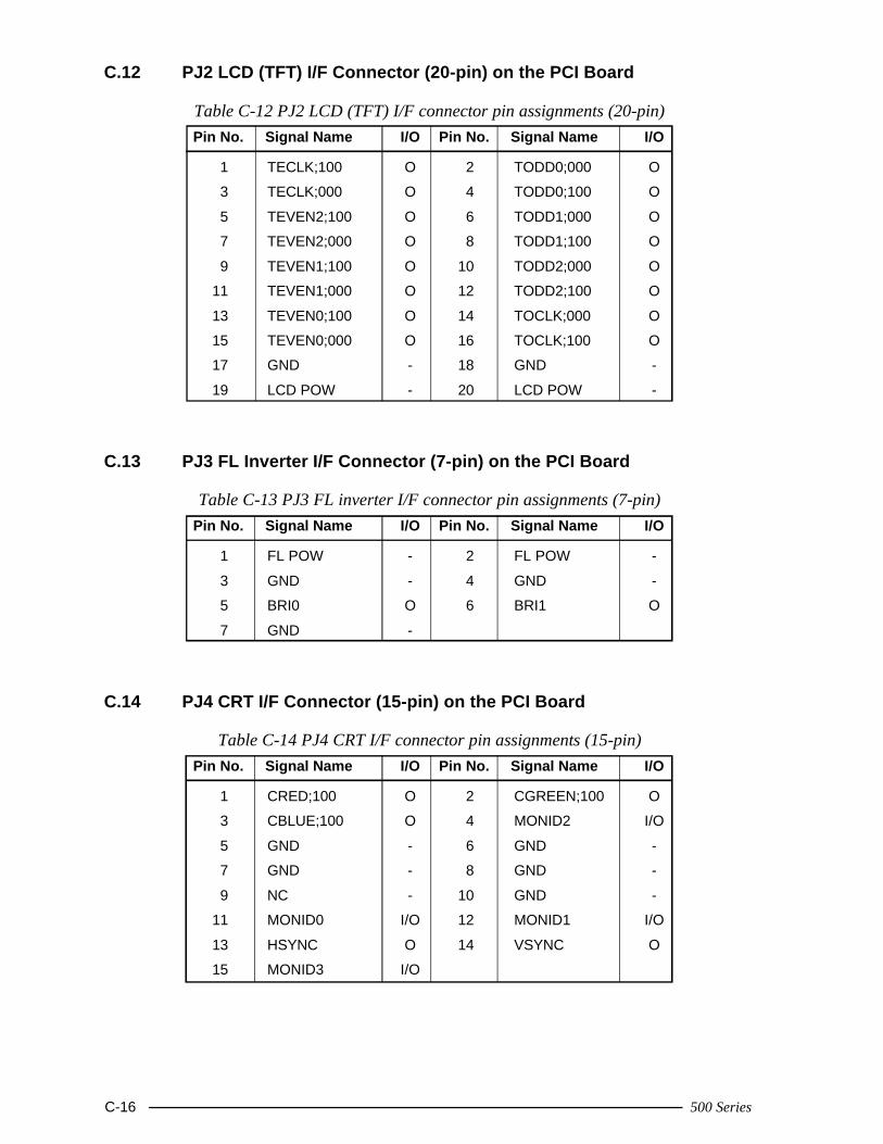
C-16 500 Series
C.12 PJ2 LCD (TFT) I/F Connector (20-pin) on the PCI Board
Table C-12 PJ2 LCD (TFT) I/F connector pin assignments (20-pin)Pin No. Signal Name I/O Pin No. Signal Name I/O
1 TECLK;100 O 2 TODD0;000 O
3 TECLK;000 O 4 TODD0;100 O
5 TEVEN2;100 O 6 TODD1;000 O
7 TEVEN2;000 O 8 TODD1;100 O
9 TEVEN1;100 O 10 TODD2;000 O
11 TEVEN1;000 O 12 TODD2;100 O
13 TEVEN0;100 O 14 TOCLK;000 O
15 TEVEN0;000 O 16 TOCLK;100 O
17 GND - 18 GND -
19 LCD POW - 20 LCD POW -
C.13 PJ3 FL Inverter I/F Connector (7-pin) on the PCI Board
Table C-13 PJ3 FL inverter I/F connector pin assignments (7-pin)Pin No. Signal Name I/O Pin No. Signal Name I/O
1 FL POW - 2 FL POW -
3 GND - 4 GND -
5 BRI0 O 6 BRI1 O
7 GND -
C.14 PJ4 CRT I/F Connector (15-pin) on the PCI Board
Table C-14 PJ4 CRT I/F connector pin assignments (15-pin)Pin No. Signal Name I/O Pin No. Signal Name I/O
1 CRED;100 O 2 CGREEN;100 O
3 CBLUE;100 O 4 MONID2 I/O
5 GND - 6 GND -
7 GND - 8 GND -
9 NC - 10 GND -
11 MONID0 I/O 12 MONID1 I/O
13 HSYNC O 14 VSYNC O
15 MONID3 I/O
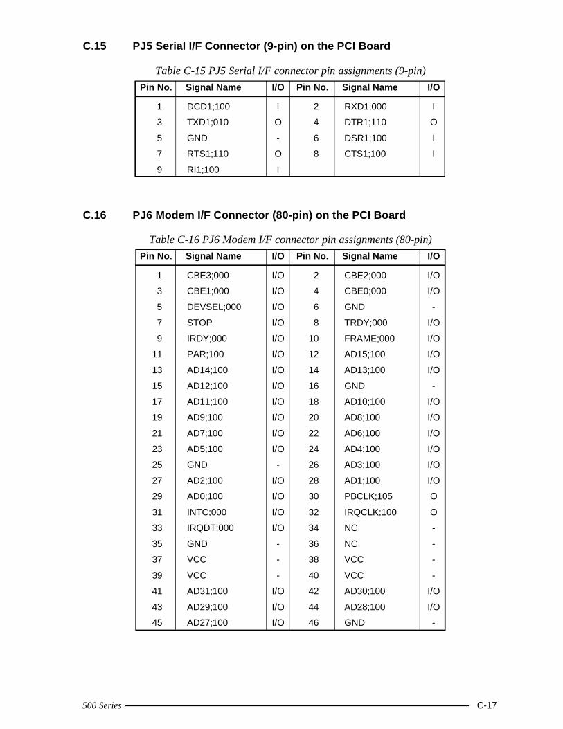
500 Series C-17
C.15 PJ5 Serial I/F Connector (9-pin) on the PCI Board
Table C-15 PJ5 Serial I/F connector pin assignments (9-pin)Pin No. Signal Name I/O Pin No. Signal Name I/O
1 DCD1;100 I 2 RXD1;000 I
3 TXD1;010 O 4 DTR1;110 O
5 GND - 6 DSR1;100 I
7 RTS1;110 O 8 CTS1;100 I
9 RI1;100 I
C.16 PJ6 Modem I/F Connector (80-pin) on the PCI Board
Table C-16 PJ6 Modem I/F connector pin assignments (80-pin)Pin No. Signal Name I/O Pin No. Signal Name I/O
1 CBE3;000 I/O 2 CBE2;000 I/O
3 CBE1;000 I/O 4 CBE0;000 I/O
5 DEVSEL;000 I/O 6 GND -
7 STOP I/O 8 TRDY;000 I/O
9 IRDY;000 I/O 10 FRAME;000 I/O
11 PAR;100 I/O 12 AD15;100 I/O
13 AD14;100 I/O 14 AD13;100 I/O
15 AD12;100 I/O 16 GND -
17 AD11;100 I/O 18 AD10;100 I/O
19 AD9;100 I/O 20 AD8;100 I/O
21 AD7;100 I/O 22 AD6;100 I/O
23 AD5;100 I/O 24 AD4;100 I/O
25 GND - 26 AD3;100 I/O
27 AD2;100 I/O 28 AD1;100 I/O
29 AD0;100 I/O 30 PBCLK;105 O
31 INTC;000 I/O 32 IRQCLK;100 O
33 IRQDT;000 I/O 34 NC -
35 GND - 36 NC -
37 VCC - 38 VCC -
39 VCC - 40 VCC -
41 AD31;100 I/O 42 AD30;100 I/O
43 AD29;100 I/O 44 AD28;100 I/O
45 AD27;100 I/O 46 GND -
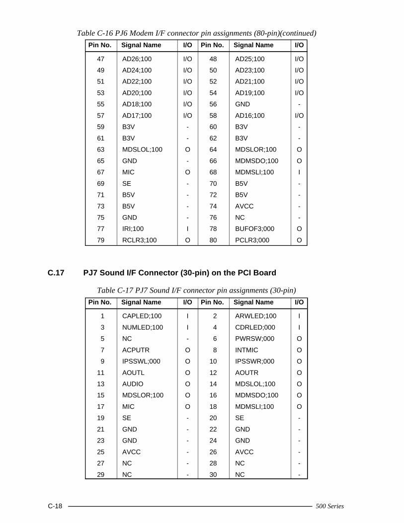
C-18 500 Series
Table C-16 PJ6 Modem I/F connector pin assignments (80-pin)(continued)Pin No. Signal Name I/O Pin No. Signal Name I/O
47 AD26;100 I/O 48 AD25;100 I/O
49 AD24;100 I/O 50 AD23;100 I/O
51 AD22;100 I/O 52 AD21;100 I/O
53 AD20;100 I/O 54 AD19;100 I/O
55 AD18;100 I/O 56 GND -
57 AD17;100 I/O 58 AD16;100 I/O
59 B3V - 60 B3V -
61 B3V - 62 B3V -
63 MDSLOL;100 O 64 MDSLOR;100 O
65 GND - 66 MDMSDO;100 O
67 MIC O 68 MDMSLI;100 I
69 SE - 70 B5V -
71 B5V - 72 B5V -
73 B5V - 74 AVCC -
75 GND - 76 NC -
77 IRI;100 I 78 BUFOF3;000 O
79 RCLR3;100 O 80 PCLR3;000 O
C.17 PJ7 Sound I/F Connector (30-pin) on the PCI Board
Table C-17 PJ7 Sound I/F connector pin assignments (30-pin)Pin No. Signal Name I/O Pin No. Signal Name I/O
1 CAPLED;100 I 2 ARWLED;100 I
3 NUMLED;100 I 4 CDRLED;000 I
5 NC - 6 PWRSW;000 O
7 ACPUTR O 8 INTMIC O
9 IPSSWL;000 O 10 IPSSWR;000 O
11 AOUTL O 12 AOUTR O
13 AUDIO O 14 MDSLOL;100 O
15 MDSLOR;100 O 16 MDMSDO;100 O
17 MIC O 18 MDMSLI;100 O
19 SE - 20 SE -
21 GND - 22 GND -
23 GND - 24 GND -
25 AVCC - 26 AVCC -
27 NC - 28 NC -
29 NC - 30 NC -
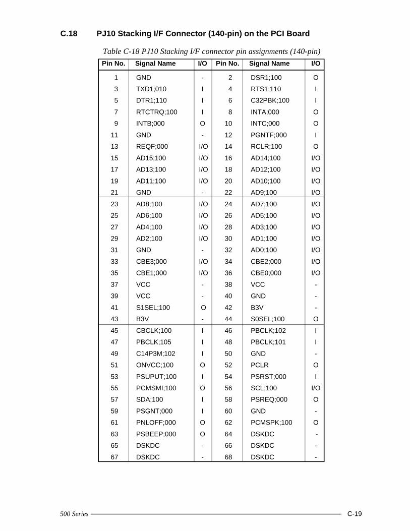
500 Series C-19
C.18 PJ10 Stacking I/F Connector (140-pin) on the PCI Board
Table C-18 PJ10 Stacking I/F connector pin assignments (140-pin)Pin No. Signal Name I/O Pin No. Signal Name I/O
1 GND - 2 DSR1;100 O
3 TXD1;010 I 4 RTS1;110 I
5 DTR1;110 I 6 C32PBK;100 I
7 RTCTRQ;100 I 8 INTA;000 O
9 INTB;000 O 10 INTC;000 O
11 GND - 12 PGNTF;000 I
13 REQF;000 I/O 14 RCLR;100 O
15 AD15;100 I/O 16 AD14;100 I/O
17 AD13;100 I/O 18 AD12;100 I/O
19 AD11;100 I/O 20 AD10;100 I/O
21 GND - 22 AD9;100 I/O
23 AD8;100 I/O 24 AD7;100 I/O
25 AD6;100 I/O 26 AD5;100 I/O
27 AD4;100 I/O 28 AD3;100 I/O
29 AD2;100 I/O 30 AD1;100 I/O
31 GND - 32 AD0;100 I/O
33 CBE3;000 I/O 34 CBE2;000 I/O
35 CBE1;000 I/O 36 CBE0;000 I/O
37 VCC - 38 VCC -
39 VCC - 40 GND -
41 S1SEL;100 O 42 B3V -
43 B3V - 44 S0SEL;100 O
45 CBCLK;100 I 46 PBCLK;102 I
47 PBCLK;105 I 48 PBCLK;101 I
49 C14P3M;102 I 50 GND -
51 ONVCC;100 O 52 PCLR O
53 PSUPUT;100 I 54 PSRST;000 I
55 PCMSMI;100 O 56 SCL;100 I/O
57 SDA;100 I 58 PSREQ;000 O
59 PSGNT;000 I 60 GND -
61 PNLOFF;000 O 62 PCMSPK;100 O
63 PSBEEP;000 O 64 DSKDC -
65 DSKDC - 66 DSKDC -
67 DSKDC - 68 DSKDC -
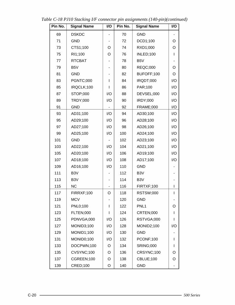
C-20 500 Series
Table C-18 PJ10 Stacking I/F connector pin assignments (140-pin)(continued)Pin No. Signal Name I/O Pin No. Signal Name I/O
69 DSKDC - 70 GND -
71 GND - 72 DCD1;100 O
73 CTS1;100 O 74 RXD1;000 O
75 RI1;100 O 76 INLED;100 I
77 RTCBAT - 78 B5V -
79 B5V - 80 REQC;000 O
81 GND - 82 BUFOFF;100 O
83 PGNTC;000 I 84 IRQDT;000 I/O
85 IRQCLK;100 I 86 PAR;100 I/O
87 STOP;000 I/O 88 DEVSEL;000 I/O
89 TRDY;000 I/O 90 IRDY;000 I/O
91 GND - 92 FRAME;000 I/O
93 AD31;100 I/O 94 AD30;100 I/O
95 AD29;100 I/O 96 AD28;100 I/O
97 AD27;100 I/O 98 AD26;100 I/O
99 AD25;100 I/O 100 AD24;100 I/O
101 GND - 102 AD23;100 I/O
103 AD22;100 I/O 104 AD21;100 I/O
105 AD20;100 I/O 106 AD19;100 I/O
107 AD18;100 I/O 108 AD17;100 I/O
109 AD16;100 I/O 110 GND -
111 B3V - 112 B3V -
113 B3V - 114 B3V -
115 NC - 116 FIRTXF;100 I
117 FIRRXF;100 O 118 RSTSW;000 I
119 MCV - 120 GND -
121 PNL0;100 I 122 PNL1 O
123 FLTEN;000 I 124 CRTEN;000 I
125 PDNVGA;000 I/O 126 RSTVGA;000 I
127 MONID3;100 I/O 128 MONID2;100 I/O
129 MONID1;100 I/O 130 GND -
131 MONID0;100 I/O 132 PCONF;100 I
133 DOCPWN;100 O 134 SRING;000 I
135 CVSYNC;100 O 136 CRSYNC;100 O
137 CGREEN;100 O 138 CBLUE;100 O
139 CRED;100 O 140 GND -
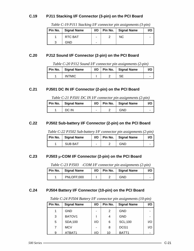
500 Series C-21
C.19 PJ11 Stacking I/F Connector (3-pin) on the PCI Board
Table C-19 PJ11 Stacking I/F connector pin assignments (3-pin)Pin No. Signal Name I/O Pin No. Signal Name I/O
1 RTC BAT - 2 NC -
3 GND -
C.20 PJ12 Sound I/F Connector (2-pin) on the PCI Board
Table C-20 PJ12 Sound I/F connector pin assignments (2-pin)Pin No. Signal Name I/O Pin No. Signal Name I/O
1 INTMIC I 2 SE -
C.21 PJ501 DC IN I/F Connector (2-pin) on the PCI Board
Table C-21 PJ501 DC IN I/F connector pin assignments (2-pin)Pin No. Signal Name I/O Pin No. Signal Name I/O
1 DC IN - 2 GND -
C.22 PJ502 Sub-battery I/F Connector (2-pin) on the PCI Board
Table C-22 PJ502 Sub-battery I/F connector pin assignments (2-pin)Pin No. Signal Name I/O Pin No. Signal Name I/O
1 SUB BAT - 2 GND -
C.23 PJ503 µµ-COM I/F Connector (2-pin) on the PCI Board
Table C-23 PJ503 -COM I/F connector pin assignments (2-pin)Pin No. Signal Name I/O Pin No. Signal Name I/O
1 PNLOFF;000 I 2 GND -
C.24 PJ504 Battery I/F Connector (10-pin) on the PCI Board
Table C-24 PJ504 Battery I/F connector pin assignments (10-pin)Pin No. Signal Name I/O Pin No. Signal Name I/O
1 GND - 2 GND -
3 BATOV1 I 4 GND -
5 SDA;100 I/O 6 SCL;100 I/O
7 MCV - 8 DCG1 I/O
9 ATBAT1 I/O 10 BATT1 -
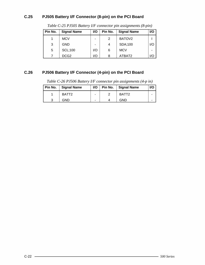
C-22 500 Series
C.25 PJ505 Battery I/F Connector (8-pin) on the PCI Board
Table C-25 PJ505 Battery I/F connector pin assignments (8-pin)Pin No. Signal Name I/O Pin No. Signal Name I/O
1 MCV - 2 BATOV2 I
3 GND - 4 SDA;100 I/O
5 SCL;100 I/O 6 MCV -
7 DCG2 I/O 8 ATBAT2 I/O
C.26 PJ506 Battery I/F Connector (4-pin) on the PCI Board
Table C-26 PJ506 Battery I/F connector pin assignments (4-p in)Pin No. Signal Name I/O Pin No. Signal Name I/O
1 BATT2 - 2 BATT2 -
3 GND - 4 GND -
500 Series C-23
C.27 PJ301 PCI Board I/F Connector (160-pin ) on the CardBus Board
Table C-27 PJ301 PCI board I/F connector pin assignments (160-pin)Pin No. Signal Name I/O Pin No. Signal Name I/O
1 NC - 2 NC -
3 NC - 4 NC -
5 BCVPP - 6 GND -
7 BCVCC - 8 BCVCC -
9 ACVPP - 10 ACVCC -
11 ACVCC - 12 BCCD1;000 I
13 BCCD2;000 I 14 BCINT;000 I
15 BCREQ;000 I 16 GND -
17 BCAUDI;100 I 18 BCSTSC;100 I
19 BCGNT;000 I/O 20 BCAD11;100 I/O
21 BCVS1;100 I/O 22 BCVS2;100 I/O
23 BCCBE0;000 I/O 24 BCAD10;100 I/O
25 BCAD13;100 I/O 26 GND -
27 BCAD15;100 I/O 28 BCRST;000 O
29 BCCLKR;000 I/O 30 BCSERR;000 I/O
31 BCCBE3;000 I/O 32 BCAD27;100 I/O
33 BCAD29;100 I/O 34 BCD2;100 I/O
35 BCAD0;100 I/O 36 GND -
37 BCAD1;100 I/O 38 BCAD3;100 I/O
39 BCAD5;100 I/O 40 BCAD7;100 I/O
41 BCAD26;100 I/O 42 BCAD25;100 I/O
43 BCAD24;100 I/O 44 BCAD23;100 I/O
45 GND - 46 BCAD22;100 I/O
47 BCAD21;100 I/O 48 BCAD20;100 I/O
49 BCAD18;100 I/O 50 BCAD28;100 I/O
51 BCAD30;100 I/O 52 BCAD31;100 I/O
53 BCAD2;100 I/O 54 BCAD4;100 I/O
55 GND - 56 BCAD6;100 I/O
57 BCD14;100 I/O 58 BCAD8;100 I/O
59 BCCBE1;000 I/O 60 BCAD14;100 I/O
61 BCAD9;100 I/O 62 BCAD12;100 I/O
63 BCCBE2;000 I/O 64 BCPAR;100 I/O
65 GND - 66 BCPERR;000 I/O
67 BCIRDY;000 I/O 68 BCCLK;100 I/O
C-24 500 Series
Table C-27 PJ301 PCI board I/F connector pin assignments (160-pin)(continued)Pin No. Signal Name I/O Pin No. Signal Name I/O
69 BCAD16;100 I/O 70 BCA18;100 I/O
71 BCLOCK;000 I/O 72 BCSTOP;000 I/O
73 BCDEVS;000 I/O 74 BCTRDY;000 I/O
75 GND - 76 BCFRAM;000 I/O
77 BCAD17;100 I/O 78 BCAD19;100 I/O
79 NC - 80 IPSSWR I/O
81 NC - 82 NC -
83 NC - 84 NC -
85 BCVPP - 86 GND -
87 BCVCC - 88 BCVCC -
89 ACVPP - 90 ACVCC -
91 ACVCC - 92 ACCD1;000 I
93 ACCD2;000 I 94 AACINT;000 I
95 ACREQ;000 I 96 GND -
97 ACAUDI;100 I 98 ACSTSC;100 I
99 ACGNT;000 I/O 100 ACAD11;100 I/O
101 ACVS1;100 I/O 102 ACVS2;100 I/O
103 ACCBE0;000 I/O 104 ACAD10;100 I/O
105 ACAD13;100 I/O 106 GND -
107 ACAD15;100 I/O 108 ACRST;000 I/O
109 ACCLKR;000 I/O 110 ACSERR;000 I/O
111 ACCBE3;000 I/O 112 ACAD26;100 I/O
113 ACAD25;100 I/O 114 ACAD24;100 I/O
115 ACAD23;100 I/O 116 GND -
117 ACAD22;100 I/O 118 ACAD21;100 I/O
119 ACAD20;100 I/O 120 ACAD18;100 I/O
121 ACAD28;100 I/O 122 ACAD30;100 I/O
123 ACAD31;100 I/O 124 ACAD2;100 I/O
125 GND - 126 ACAD4;100 I/O
127 ACAD6;100 I/O 128 ACD14;100 I/O
129 ACAD8;100 I/O 130 ACAD27;100 I/O
131 ACAD29;100 I/O 132 ACD2;100 I/O
133 ACAD0;100 I/O 134 ACAD1;100 I/O
135 GND - 136 ACAD3;100 I/O
137 ACAD5;100 I/O 138 ACAD7;100 I/O
139 ACCBE1;000 I/O 140 ACAD14;100 I/O
500 Series C-25
Table C-27 PJ301 PCI board I/F connector pin assignments (160-pin)(continued)Pin No. Signal Name I/O Pin No. Signal Name I/O
141 ACAD9;100 I/O 142 ACAD12;100 I/O
143 ACCBE2;000 I/O 144 ACPAR;100 I/O
145 GND - 146 ACPERR;000 I/O
147 ACIRDY;000 I/O 148 ACCLK;100 I/O
149 ACAD16;100 I/O 150 ACA18;100 I/O
151 ACLOCK;000 I/O 152 ACSTOP;000 I/O
153 ACDEVS;000 I/O 154 ACTRDY;000 I/O
155 GND - 156 ACFRAM;000 I/O
157 ACAD17;100 I/O 158 ACAD19;100 I/O
159 NC - 160 IPSSWL -
C.28 PJ302 PCI Board I/F Connector (4-pin ) on the CardBus Board
Table C-28 PJ302 PCI board I/F connector pin assignments (4-pin)Pin No. Signal Name I/O Pin No. Signal Name I/O
1 GND - 2 IPSSWR I
3 GND - 4 IPSSWL I
C.29 PJ303 Card Slot I/F Connector (152-pin ) on the CardBus Board
Table C-29 PJ303 Card slot I/F connector pin assignments (152-pin)Pin No. Signal Name I/O Pin No. Signal Name I/O
A01 GND - A02 BCAD0;100 I/O
A03 BCAD1;100 I/O A04 BCAD3;100 I/O
A05 BCAD5;100 I/O A06 BCAD7;100 I/O
A07 BCCBE0;000 I/O A08 BCAD9;100 I/O
A09 BCAD11;100 I/O A10 BCAD12;100 I/O
A11 BCAD14;100 I/O A12 BCCBE1;000 I/O
A13 BCPAR;100 I/O A14 BCPERR;000 I/O
A15 BCGNT;000 I A16 BCINT;000 O
A17 BCVCC - A18 BCVPP -
A19 BCCLK;100 I A20 BCIRDY;000 I/O
A21 BCCBE2;000 I/O A22 BCAD18;100 I/O
A23 BCAD20;100 I/O A24 BCAD21;100 I/O
A25 BCAD22;100 I/O A26 BCAD23;100 I/O
A27 BCAD24;100 I/O A28 BCAD25;100 I/O
C-26 500 Series
Table C-29 PJ303 Card slot I/F connector pin assignments (152-pin)(continued)Pin No. Signal Name I/O Pin No. Signal Name I/O
A29 BCAD26;100 I/O A30 BCAD27;100 I/O
A31 BCAD29;100 I/O A32 BCD2;100 I/O
A33 BCCLKR;000 I/O A34 GND -
A35 GND - A36 BCCD1;000 O
A37 BCAD2;100 I/O A38 BCAD4;100 I/O
A39 BCAD6;100 I/O A40 BCD14;100 I/O
A41 BCAD8;100 I/O A42 BCAD10;100 I/O
A43 BCVS1;100 I/O A44 BCAD13;100 I/O
A45 BCAD15;100 I/O A46 BCAD16;100 I/O
A47 BCA18;100 I/O A48 BCLOCK;000 I/O
A49 BCSTOP;000 I/O A50 BCDEVS;000 I/O
A51 BCVCC - A52 BCVPP -
A53 BCTRDY;000 I/O A54 BCFARM;000 I/O
A55 BCAD17;100 I/O A56 BCAD18;100 I/O
A57 BCVS2;100 I/O A58 BCRST;000 I
A59 BCSERR;000 O A60 BCREQ;000 O
A61 BCCBE3;000 I/O A62 BCAUDI;100 O
A63 BCSTSC;100 O A64 BCAD28;100 I/O
A65 BCAD30;100 I/O A66 BCAD31;100 I/O
A67 BCCD2;000 I/O A68 GND -
A69 GND - A70 GND -
A71 GND - A72 GND -
A73 GND - A74 GND -
A75 GND - A76 GND -
B01 GND - B02 ACAD0;100 I/O
B03 ACAD1;100 I/O B04 ACAD3;100 I/O
B05 ACAD5;100 I/O B06 ACAD7;100 I/O
B07 ACCBE0;000 I/O B08 ACAD9;100 I/O
B09 ACAD11;100 I/O B10 ACAD12;100 I/O
B11 ACAD14;100 I/O B12 ACCBE1;000 I/O
B13 ACPAR;100 I/O B14 ACPERR;000 I/O
B15 ACGNT;000 I B16 ACINT;000 O
B17 ACVCC - B18 ACVPP -
B19 ACCLK;100 I B20 ACIRDY;000 I/O
B21 ACCBE2;000 I/O B22 ACAD18;100 I/O
B23 ACAD20;100 I/O B24 ACAD21;100 I/O
B25 ACAD22;100 I/O B26 ACAD23;100 I/O
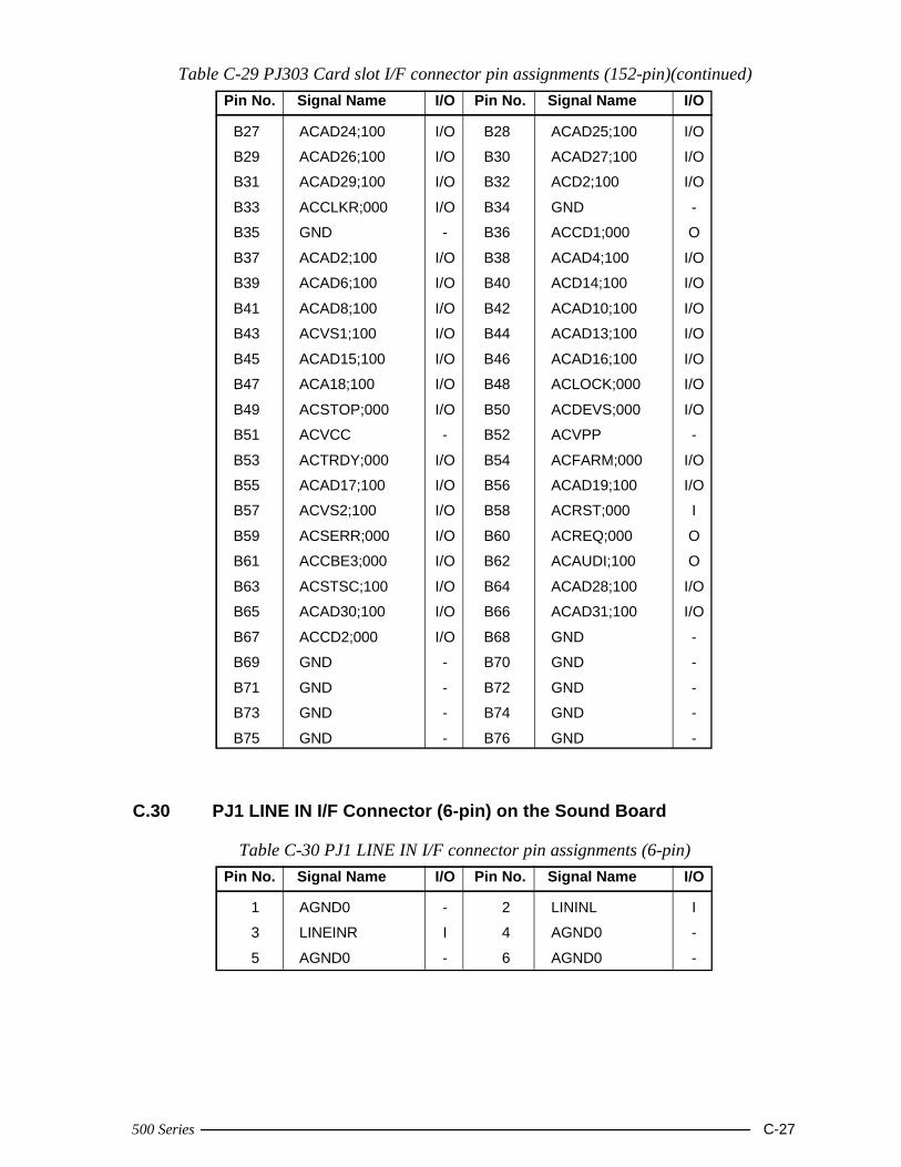
500 Series C-27
Table C-29 PJ303 Card slot I/F connector pin assignments (152-pin)(continued)Pin No. Signal Name I/O Pin No. Signal Name I/O
B27 ACAD24;100 I/O B28 ACAD25;100 I/O
B29 ACAD26;100 I/O B30 ACAD27;100 I/O
B31 ACAD29;100 I/O B32 ACD2;100 I/O
B33 ACCLKR;000 I/O B34 GND -
B35 GND - B36 ACCD1;000 O
B37 ACAD2;100 I/O B38 ACAD4;100 I/O
B39 ACAD6;100 I/O B40 ACD14;100 I/O
B41 ACAD8;100 I/O B42 ACAD10;100 I/O
B43 ACVS1;100 I/O B44 ACAD13;100 I/O
B45 ACAD15;100 I/O B46 ACAD16;100 I/O
B47 ACA18;100 I/O B48 ACLOCK;000 I/O
B49 ACSTOP;000 I/O B50 ACDEVS;000 I/O
B51 ACVCC - B52 ACVPP -
B53 ACTRDY;000 I/O B54 ACFARM;000 I/O
B55 ACAD17;100 I/O B56 ACAD19;100 I/O
B57 ACVS2;100 I/O B58 ACRST;000 I
B59 ACSERR;000 I/O B60 ACREQ;000 O
B61 ACCBE3;000 I/O B62 ACAUDI;100 O
B63 ACSTSC;100 I/O B64 ACAD28;100 I/O
B65 ACAD30;100 I/O B66 ACAD31;100 I/O
B67 ACCD2;000 I/O B68 GND -
B69 GND - B70 GND -
B71 GND - B72 GND -
B73 GND - B74 GND -
B75 GND - B76 GND -
C.30 PJ1 LINE IN I/F Connector (6-pin) on the Sound Board
Table C-30 PJ1 LINE IN I/F connector pin assignments (6-pin)Pin No. Signal Name I/O Pin No. Signal Name I/O
1 AGND0 - 2 LININL I
3 LINEINR I 4 AGND0 -
5 AGND0 - 6 AGND0 -
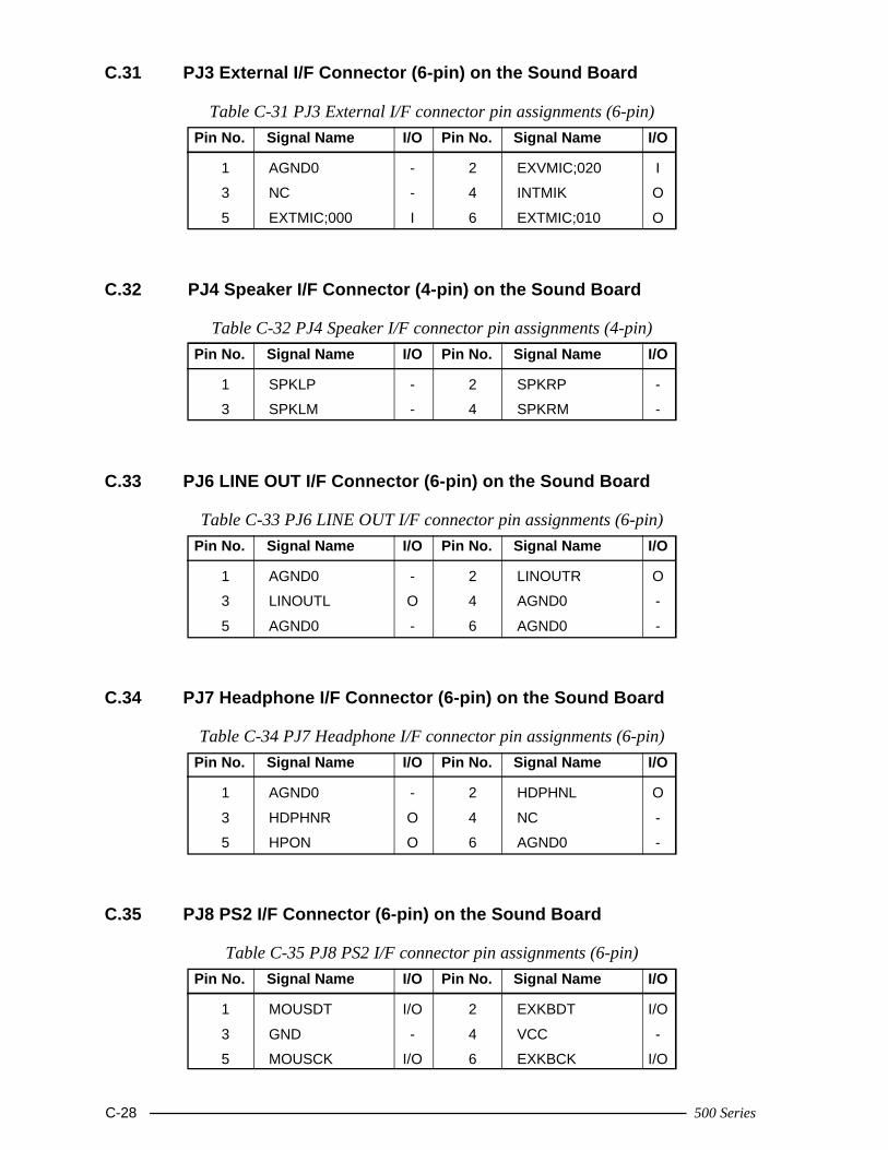
C-28 500 Series
C.31 PJ3 External I/F Connector (6-pin) on the Sound Board
Table C-31 PJ3 External I/F connector pin assignments (6-pin)Pin No. Signal Name I/O Pin No. Signal Name I/O
1 AGND0 - 2 EXVMIC;020 I
3 NC - 4 INTMIK O
5 EXTMIC;000 I 6 EXTMIC;010 O
C.32 PJ4 Speaker I/F Connector (4-pin) on the Sound Board
Table C-32 PJ4 Speaker I/F connector pin assignments (4-pin)Pin No. Signal Name I/O Pin No. Signal Name I/O
1 SPKLP - 2 SPKRP -
3 SPKLM - 4 SPKRM -
C.33 PJ6 LINE OUT I/F Connector (6-pin) on the Sound Board
Table C-33 PJ6 LINE OUT I/F connector pin assignments (6-pin)Pin No. Signal Name I/O Pin No. Signal Name I/O
1 AGND0 - 2 LINOUTR O
3 LINOUTL O 4 AGND0 -
5 AGND0 - 6 AGND0 -
C.34 PJ7 Headphone I/F Connector (6-pin) on the Sound Board
Table C-34 PJ7 Headphone I/F connector pin assignments (6-pin)Pin No. Signal Name I/O Pin No. Signal Name I/O
1 AGND0 - 2 HDPHNL O
3 HDPHNR O 4 NC -
5 HPON O 6 AGND0 -
C.35 PJ8 PS2 I/F Connector (6-pin) on the Sound Board
Table C-35 PJ8 PS2 I/F connector pin assignments (6-pin)Pin No. Signal Name I/O Pin No. Signal Name I/O
1 MOUSDT I/O 2 EXKBDT I/O
3 GND - 4 VCC -
5 MOUSCK I/O 6 EXKBCK I/O
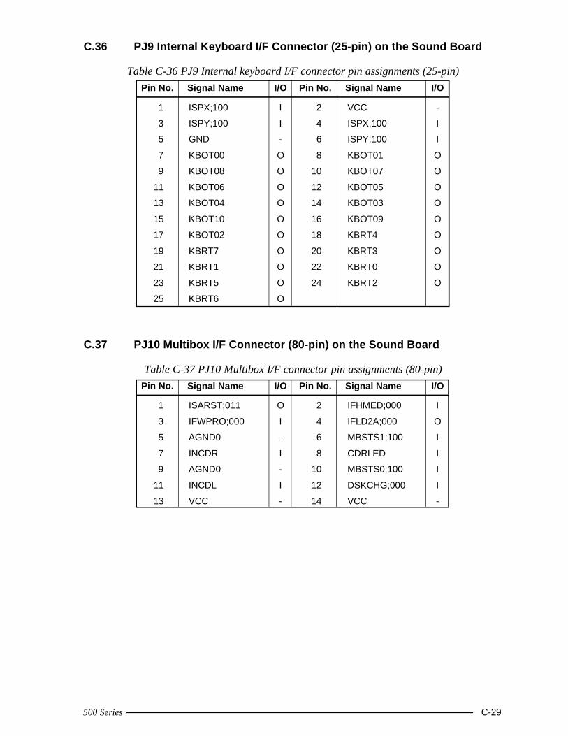
500 Series C-29
C.36 PJ9 Internal Keyboard I/F Connector (25-pin) on the Sound Board
Table C-36 PJ9 Internal keyboard I/F connector pin assignments (25-pin)Pin No. Signal Name I/O Pin No. Signal Name I/O
1 ISPX;100 I 2 VCC -
3 ISPY;100 I 4 ISPX;100 I
5 GND - 6 ISPY;100 I
7 KBOT00 O 8 KBOT01 O
9 KBOT08 O 10 KBOT07 O
11 KBOT06 O 12 KBOT05 O
13 KBOT04 O 14 KBOT03 O
15 KBOT10 O 16 KBOT09 O
17 KBOT02 O 18 KBRT4 O
19 KBRT7 O 20 KBRT3 O
21 KBRT1 O 22 KBRT0 O
23 KBRT5 O 24 KBRT2 O
25 KBRT6 O
C.37 PJ10 Multibox I/F Connector (80-pin) on the Sound Board
Table C-37 PJ10 Multibox I/F connector pin assignments (80-pin)Pin No. Signal Name I/O Pin No. Signal Name I/O
1 ISARST;011 O 2 IFHMED;000 I
3 IFWPRO;000 I 4 IFLD2A;000 O
5 AGND0 - 6 MBSTS1;100 I
7 INCDR I 8 CDRLED I
9 AGND0 - 10 MBSTS0;100 I
11 INCDL I 12 DSKCHG;000 I
13 VCC - 14 VCC -
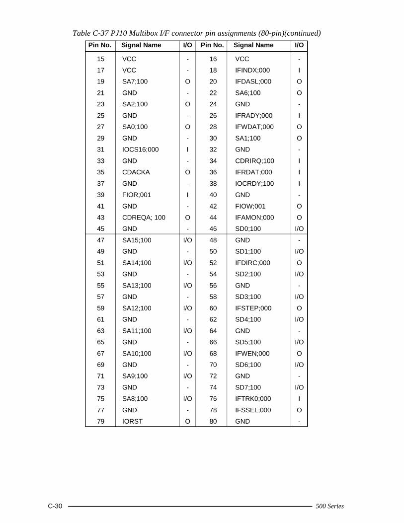
C-30 500 Series
Table C-37 PJ10 Multibox I/F connector pin assignments (80-pin)(continued)Pin No. Signal Name I/O Pin No. Signal Name I/O
15 VCC - 16 VCC -
17 VCC - 18 IFINDX;000 I
19 SA7;100 O 20 IFDASL;000 O
21 GND - 22 SA6;100 O
23 SA2;100 O 24 GND -
25 GND - 26 IFRADY;000 I
27 SA0;100 O 28 IFWDAT;000 O
29 GND - 30 SA1;100 O
31 IOCS16;000 I 32 GND -
33 GND - 34 CDRIRQ;100 I
35 CDACKA O 36 IFRDAT;000 I
37 GND - 38 IOCRDY;100 I
39 FIOR;001 I 40 GND -
41 GND - 42 FIOW;001 O
43 CDREQA; 100 O 44 IFAMON;000 O
45 GND - 46 SD0;100 I/O
47 SA15;100 I/O 48 GND -
49 GND - 50 SD1;100 I/O
51 SA14;100 I/O 52 IFDIRC;000 O
53 GND - 54 SD2;100 I/O
55 SA13;100 I/O 56 GND -
57 GND - 58 SD3;100 I/O
59 SA12;100 I/O 60 IFSTEP;000 O
61 GND - 62 SD4;100 I/O
63 SA11;100 I/O 64 GND -
65 GND - 66 SD5;100 I/O
67 SA10;100 I/O 68 IFWEN;000 O
69 GND - 70 SD6;100 I/O
71 SA9;100 I/O 72 GND -
73 GND - 74 SD7;100 I/O
75 SA8;100 I/O 76 IFTRK0;000 I
77 GND - 78 IFSSEL;000 O
79 IORST O 80 GND -
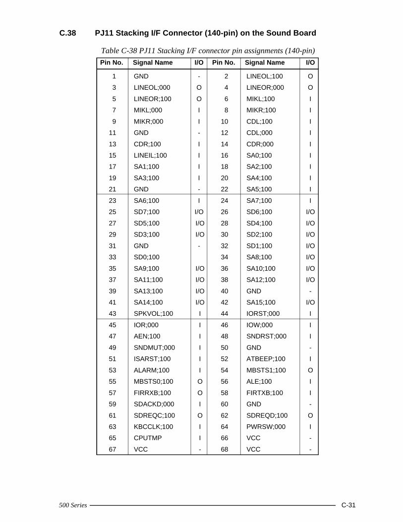
500 Series C-31
C.38 PJ11 Stacking I/F Connector (140-pin) on the Sound Board
Table C-38 PJ11 Stacking I/F connector pin assignments (140-pin)Pin No. Signal Name I/O Pin No. Signal Name I/O
1 GND - 2 LINEOL;100 O
3 LINEOL;000 O 4 LINEOR;000 O
5 LINEOR;100 O 6 MIKL;100 I
7 MIKL;000 I 8 MIKR;100 I
9 MIKR;000 I 10 CDL;100 I
11 GND - 12 CDL;000 I
13 CDR;100 I 14 CDR;000 I
15 LINEIL;100 I 16 SA0;100 I
17 SA1;100 I 18 SA2;100 I
19 SA3;100 I 20 SA4;100 I
21 GND - 22 SA5;100 I
23 SA6;100 I 24 SA7;100 I
25 SD7;100 I/O 26 SD6;100 I/O
27 SD5;100 I/O 28 SD4;100 I/O
29 SD3;100 I/O 30 SD2;100 I/O
31 GND - 32 SD1;100 I/O
33 SD0;100 34 SA8;100 I/O
35 SA9;100 I/O 36 SA10;100 I/O
37 SA11;100 I/O 38 SA12;100 I/O
39 SA13;100 I/O 40 GND -
41 SA14;100 I/O 42 SA15;100 I/O
43 SPKVOL;100 I 44 IORST;000 I
45 IOR;000 I 46 IOW;000 I
47 AEN;100 I 48 SNDRST;000 I
49 SNDMUT;000 I 50 GND -
51 ISARST;100 I 52 ATBEEP;100 I
53 ALARM;100 I 54 MBSTS1;100 O
55 MBSTS0;100 O 56 ALE;100 I
57 FIRRXB;100 O 58 FIRTXB;100 I
59 SDACKD;000 I 60 GND -
61 SDREQC;100 O 62 SDREQD;100 O
63 KBCCLK;100 I 64 PWRSW;000 I
65 CPUTMP I 66 VCC -
67 VCC - 68 VCC -
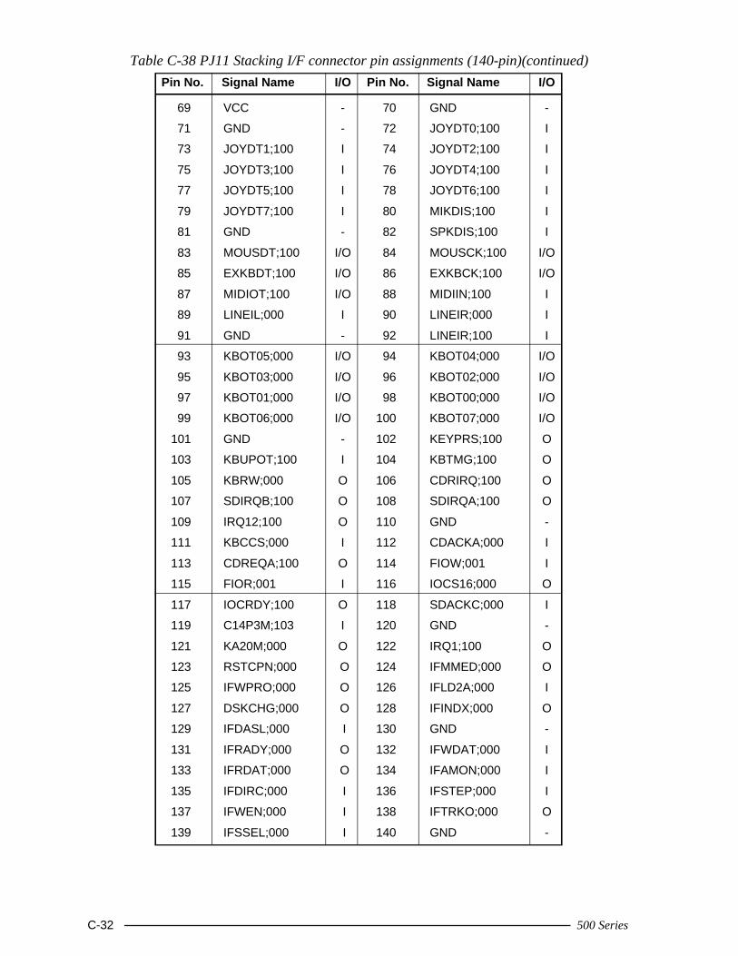
C-32 500 Series
Table C-38 PJ11 Stacking I/F connector pin assignments (140-pin)(continued)Pin No. Signal Name I/O Pin No. Signal Name I/O
69 VCC - 70 GND -
71 GND - 72 JOYDT0;100 I
73 JOYDT1;100 I 74 JOYDT2;100 I
75 JOYDT3;100 I 76 JOYDT4;100 I
77 JOYDT5;100 I 78 JOYDT6;100 I
79 JOYDT7;100 I 80 MIKDIS;100 I
81 GND - 82 SPKDIS;100 I
83 MOUSDT;100 I/O 84 MOUSCK;100 I/O
85 EXKBDT;100 I/O 86 EXKBCK;100 I/O
87 MIDIOT;100 I/O 88 MIDIIN;100 I
89 LINEIL;000 I 90 LINEIR;000 I
91 GND - 92 LINEIR;100 I
93 KBOT05;000 I/O 94 KBOT04;000 I/O
95 KBOT03;000 I/O 96 KBOT02;000 I/O
97 KBOT01;000 I/O 98 KBOT00;000 I/O
99 KBOT06;000 I/O 100 KBOT07;000 I/O
101 GND - 102 KEYPRS;100 O
103 KBUPOT;100 I 104 KBTMG;100 O
105 KBRW;000 O 106 CDRIRQ;100 O
107 SDIRQB;100 O 108 SDIRQA;100 O
109 IRQ12;100 O 110 GND -
111 KBCCS;000 I 112 CDACKA;000 I
113 CDREQA;100 O 114 FIOW;001 I
115 FIOR;001 I 116 IOCS16;000 O
117 IOCRDY;100 O 118 SDACKC;000 I
119 C14P3M;103 I 120 GND -
121 KA20M;000 O 122 IRQ1;100 O
123 RSTCPN;000 O 124 IFMMED;000 O
125 IFWPRO;000 O 126 IFLD2A;000 I
127 DSKCHG;000 O 128 IFINDX;000 O
129 IFDASL;000 I 130 GND -
131 IFRADY;000 O 132 IFWDAT;000 I
133 IFRDAT;000 O 134 IFAMON;000 I
135 IFDIRC;000 I 136 IFSTEP;000 I
137 IFWEN;000 I 138 IFTRKO;000 O
139 IFSSEL;000 I 140 GND -
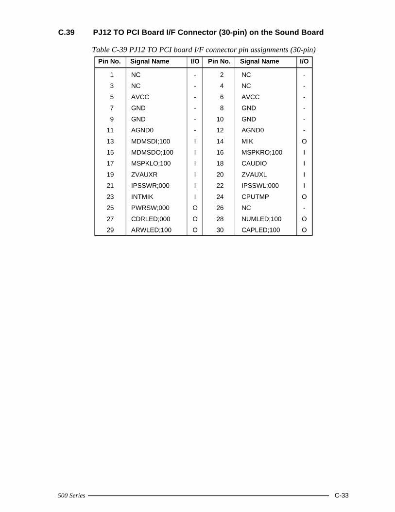
500 Series C-33
C.39 PJ12 TO PCI Board I/F Connector (30-pin) on the Sound Board
Table C-39 PJ12 TO PCI board I/F connector pin assignments (30-pin)Pin No. Signal Name I/O Pin No. Signal Name I/O
1 NC - 2 NC -
3 NC - 4 NC -
5 AVCC - 6 AVCC -
7 GND - 8 GND -
9 GND - 10 GND -
11 AGND0 - 12 AGND0 -
13 MDMSDI;100 I 14 MIK O
15 MDMSDO;100 I 16 MSPKRO;100 I
17 MSPKLO;100 I 18 CAUDIO I
19 ZVAUXR I 20 ZVAUXL I
21 IPSSWR;000 I 22 IPSSWL;000 I
23 INTMIK I 24 CPUTMP O
25 PWRSW;000 O 26 NC -
27 CDRLED;000 O 28 NUMLED;100 O
29 ARWLED;100 O 30 CAPLED;100 O
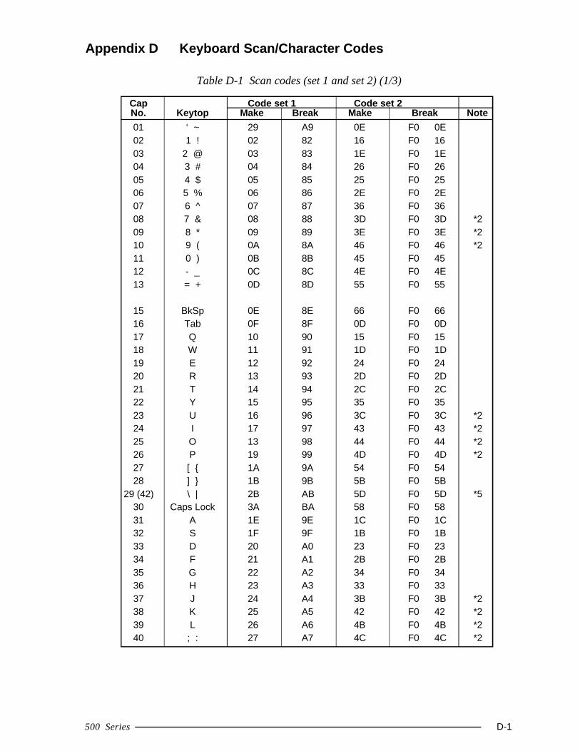
500 Series D-1
Appendix D Keyboard Scan/Character Codes
Table D-1 Scan codes (set 1 and set 2) (1/3)
Cap Code set 1 Code set 2No. Keytop Make Break Make Break Note
01 ‘ ~ 29 A9 0E F0 0E02 1 ! 02 82 16 F0 1603 2 @ 03 83 1E F0 1E04 3 # 04 84 26 F0 2605 4 $ 05 85 25 F0 2506 5 % 06 86 2E F0 2E07 6 ^ 07 87 36 F0 3608 7 & 08 88 3D F0 3D *209 8 * 09 89 3E F0 3E *210 9 ( 0A 8A 46 F0 46 *211 0 ) 0B 8B 45 F0 4512 - _ 0C 8C 4E F0 4E13 = + 0D 8D 55 F0 55
15 BkSp 0E 8E 66 F0 6616 Tab 0F 8F 0D F0 0D17 Q 10 90 15 F0 1518 W 11 91 1D F0 1D19 E 12 92 24 F0 2420 R 13 93 2D F0 2D21 T 14 94 2C F0 2C22 Y 15 95 35 F0 3523 U 16 96 3C F0 3C *224 I 17 97 43 F0 43 *225 O 13 98 44 F0 44 *226 P 19 99 4D F0 4D *227 [ { 1A 9A 54 F0 5428 ] } 1B 9B 5B F0 5B
29 (42) \ | 2B AB 5D F0 5D *530 Caps Lock 3A BA 58 F0 5831 A 1E 9E 1C F0 1C32 S 1F 9F 1B F0 1B33 D 20 A0 23 F0 2334 F 21 A1 2B F0 2B35 G 22 A2 34 F0 3436 H 23 A3 33 F0 3337 J 24 A4 3B F0 3B *238 K 25 A5 42 F0 42 *239 L 26 A6 4B F0 4B *240 ; : 27 A7 4C F0 4C *2
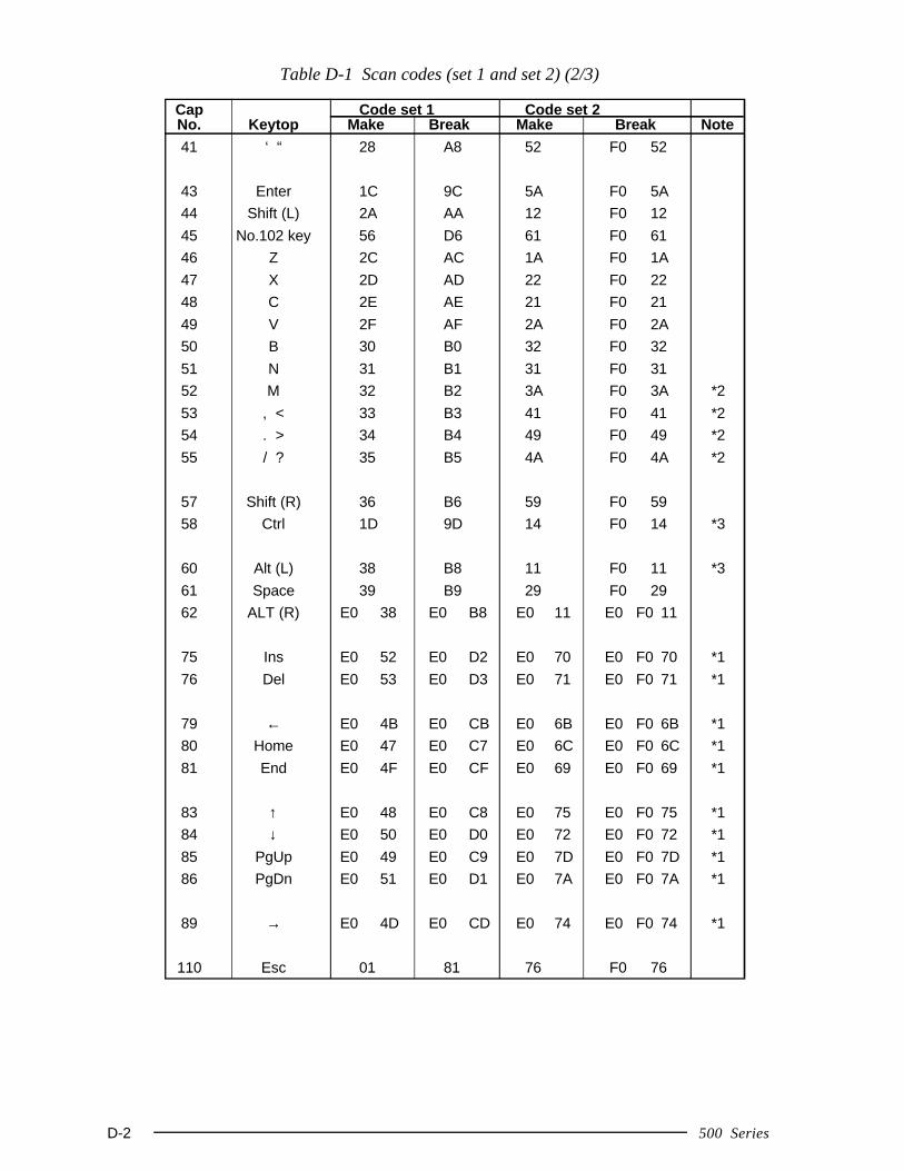
D-2 500 Series
Table D-1 Scan codes (set 1 and set 2) (2/3)
Cap Code set 1 Code set 2No. Keytop Make Break Make Break Note
41 ‘ “ 28 A8 52 F0 52
43 Enter 1C 9C 5A F0 5A
44 Shift (L) 2A AA 12 F0 12
45 No.102 key 56 D6 61 F0 61
46 Z 2C AC 1A F0 1A
47 X 2D AD 22 F0 22
48 C 2E AE 21 F0 21
49 V 2F AF 2A F0 2A
50 B 30 B0 32 F0 32
51 N 31 B1 31 F0 31
52 M 32 B2 3A F0 3A *2
53 , < 33 B3 41 F0 41 *2
54 . > 34 B4 49 F0 49 *2
55 / ? 35 B5 4A F0 4A *2
57 Shift (R) 36 B6 59 F0 59
58 Ctrl 1D 9D 14 F0 14 *3
60 Alt (L) 38 B8 11 F0 11 *3
61 Space 39 B9 29 F0 29
62 ALT (R) E0 38 E0 B8 E0 11 E0 F0 11
75 Ins E0 52 E0 D2 E0 70 E0 F0 70 *1
76 Del E0 53 E0 D3 E0 71 E0 F0 71 *1
79 ← E0 4B E0 CB E0 6B E0 F0 6B *1
80 Home E0 47 E0 C7 E0 6C E0 F0 6C *1
81 End E0 4F E0 CF E0 69 E0 F0 69 *1
83 ↑ E0 48 E0 C8 E0 75 E0 F0 75 *1
84 ↓ E0 50 E0 D0 E0 72 E0 F0 72 *1
85 PgUp E0 49 E0 C9 E0 7D E0 F0 7D *1
86 PgDn E0 51 E0 D1 E0 7A E0 F0 7A *1
89 → E0 4D E0 CD E0 74 E0 F0 74 *1
110 Esc 01 81 76 F0 76
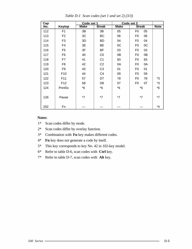
500 Series D-3
Table D-1 Scan codes (set 1 and set 2) (3/3)
Cap Code set 1 Code set 2No. Keytop Make Break Make Break Note
112 F1 3B 3B 05 F0 05
113 F2 3C BC 06 F0 06
114 F3 3D BD 04 F0 04
115 F4 3E BE 0C F0 0C
116 F5 3F BF 03 F0 03
117 F6 40 C0 0B F0 0B
118 F7 41 C1 83 F0 83
119 F8 42 C2 0A F0 0A
120 F9 43 C3 01 F0 01
121 F10 44 C4 09 F0 09
122 F11 57 D7 78 F0 78 *3
123 F12 58 D8 07 F0 07 *3
124 PrintSc *6 *6 *6 *6 *6
126 Pause *7 *7 *7 *7 *7
202 Fn — — — — *4
Notes:1* Scan codes differ by mode.2* Scan codes differ by overlay function.3* Combination with Fn key makes different codes.4* Fn key does not generate a code by itself.5* This key corresponds to key No. 42 in 102-key model.6* Refer to table D-6, scan codes with Ctrl key.7* Refer to table D-7, scan codes with Alt key.
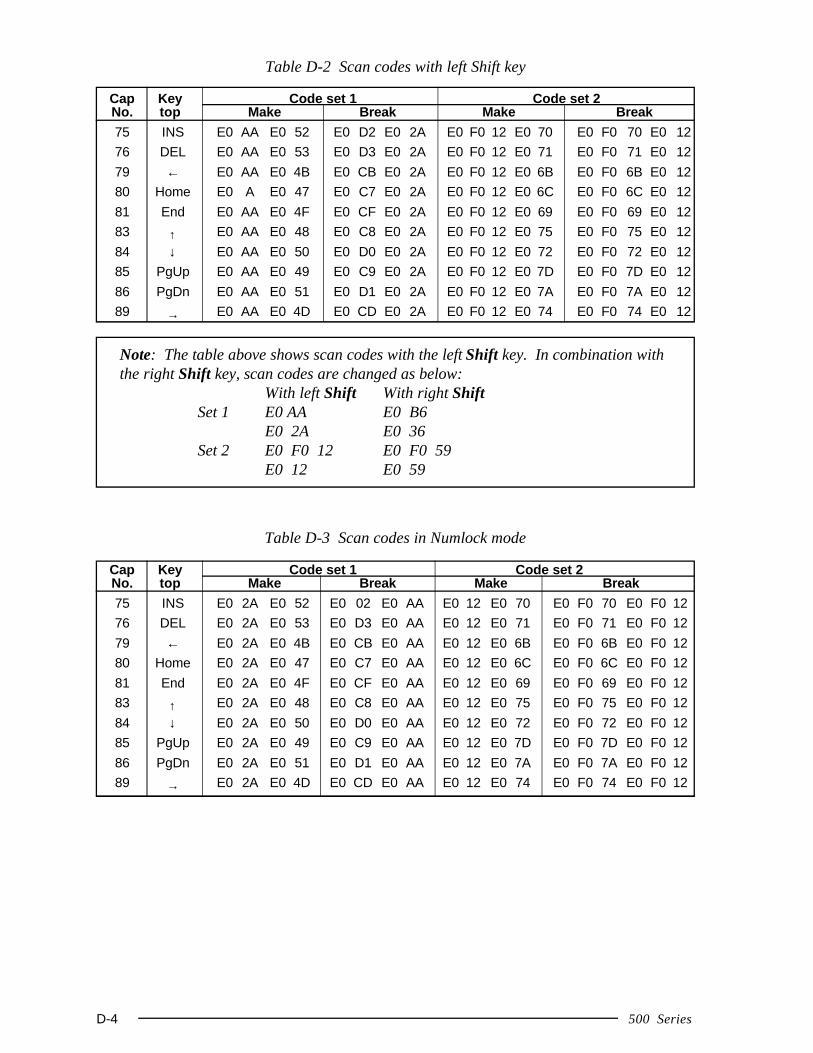
D-4 500 Series
Table D-2 Scan codes with left Shift key
Cap Key Code set 1 Code set 2No. top Make Break Make Break
75 INS E0 AA E0 52 E0 D2 E0 2A E0 F0 12 E0 70 E0 F0 70 E0 12
76 DEL E0 AA E0 53 E0 D3 E0 2A E0 F0 12 E0 71 E0 F0 71 E0 12
79 ← E0 AA E0 4B E0 CB E0 2A E0 F0 12 E0 6B E0 F0 6B E0 12
80 Home E0 A E0 47 E0 C7 E0 2A E0 F0 12 E0 6C E0 F0 6C E0 12
81 End E0 AA E0 4F E0 CF E0 2A E0 F0 12 E0 69 E0 F0 69 E0 12
83 ↑ E0 AA E0 48 E0 C8 E0 2A E0 F0 12 E0 75 E0 F0 75 E0 12
84 ↓ E0 AA E0 50 E0 D0 E0 2A E0 F0 12 E0 72 E0 F0 72 E0 12
85 PgUp E0 AA E0 49 E0 C9 E0 2A E0 F0 12 E0 7D E0 F0 7D E0 12
86 PgDn E0 AA E0 51 E0 D1 E0 2A E0 F0 12 E0 7A E0 F0 7A E0 12
89 → E0 AA E0 4D E0 CD E0 2A E0 F0 12 E0 74 E0 F0 74 E0 12
Note: The table above shows scan codes with the left Shift key. In combination withthe right Shift key, scan codes are changed as below:
With left Shift With right ShiftSet 1 E0 AA E0 B6
E0 2A E0 36Set 2 E0 F0 12 E0 F0 59
E0 12 E0 59
Table D-3 Scan codes in Numlock mode
Cap Key Code set 1 Code set 2No. top Make Break Make Break
75 INS E0 2A E0 52 E0 02 E0 AA E0 12 E0 70 E0 F0 70 E0 F0 12
76 DEL E0 2A E0 53 E0 D3 E0 AA E0 12 E0 71 E0 F0 71 E0 F0 12
79 ← E0 2A E0 4B E0 CB E0 AA E0 12 E0 6B E0 F0 6B E0 F0 12
80 Home E0 2A E0 47 E0 C7 E0 AA E0 12 E0 6C E0 F0 6C E0 F0 12
81 End E0 2A E0 4F E0 CF E0 AA E0 12 E0 69 E0 F0 69 E0 F0 12
83 ↑ E0 2A E0 48 E0 C8 E0 AA E0 12 E0 75 E0 F0 75 E0 F0 12
84 ↓ E0 2A E0 50 E0 D0 E0 AA E0 12 E0 72 E0 F0 72 E0 F0 12
85 PgUp E0 2A E0 49 E0 C9 E0 AA E0 12 E0 7D E0 F0 7D E0 F0 12
86 PgDn E0 2A E0 51 E0 D1 E0 AA E0 12 E0 7A E0 F0 7A E0 F0 12
89 → E0 2A E0 4D E0 CD E0 AA E0 12 E0 74 E0 F0 74 E0 F0 12
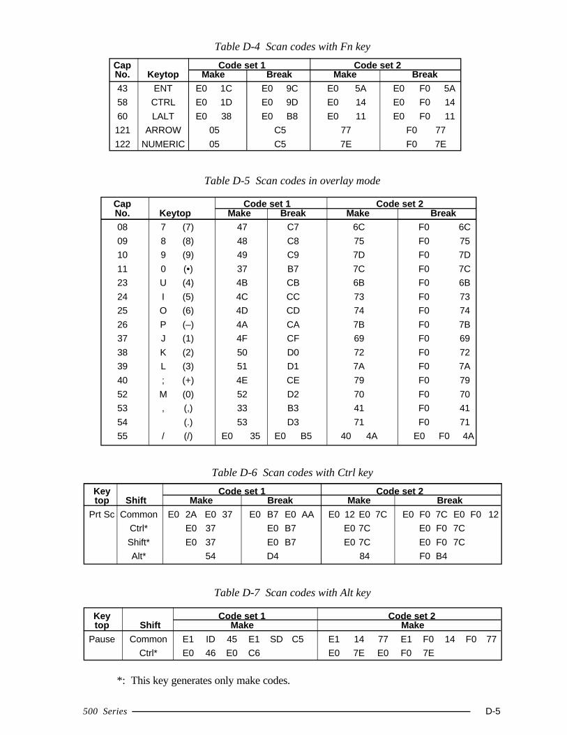
500 Series D-5
Table D-4 Scan codes with Fn key
Cap Code set 1 Code set 2No. Keytop Make Break Make Break
43 ENT E0 1C E0 9C E0 5A E0 F0 5A
58 CTRL E0 1D E0 9D E0 14 E0 F0 14
60 LALT E0 38 E0 B8 E0 11 E0 F0 11
121 ARROW 05 C5 77 F0 77
122 NUMERIC 05 C5 7E F0 7E
Table D-5 Scan codes in overlay mode
Cap Code set 1 Code set 2No. Keytop Make Break Make Break08 7 (7) 47 C7 6C F0 6C
09 8 (8) 48 C8 75 F0 75
10 9 (9) 49 C9 7D F0 7D
11 0 (•) 37 B7 7C F0 7C
23 U (4) 4B CB 6B F0 6B
24 I (5) 4C CC 73 F0 73
25 O (6) 4D CD 74 F0 74
26 P (–) 4A CA 7B F0 7B
37 J (1) 4F CF 69 F0 69
38 K (2) 50 D0 72 F0 72
39 L (3) 51 D1 7A F0 7A
40 ; (+) 4E CE 79 F0 79
52 M (0) 52 D2 70 F0 70
53 , (,) 33 B3 41 F0 41
54 (.) 53 D3 71 F0 71
55 / (/) E0 35 E0 B5 40 4A E0 F0 4A
Table D-6 Scan codes with Ctrl key
Key Code set 1 Code set 2top Shift Make Break Make Break
Prt Sc Common E0 2A E0 37 E0 B7 E0 AA E0 12 E0 7C E0 F0 7C E0 F0 12
Ctrl* E0 37 E0 B7 E0 7C E0 F0 7C
Shift* E0 37 E0 B7 E0 7C E0 F0 7C
Alt* 54 D4 84 F0 B4
Table D-7 Scan codes with Alt key
Key Code set 1 Code set 2top Shift Make Make
Pause Common E1 ID 45 E1 SD C5 E1 14 77 E1 F0 14 F0 77
Ctrl* E0 46 E0 C6 E0 7E E0 F0 7E
*: This key generates only make codes.
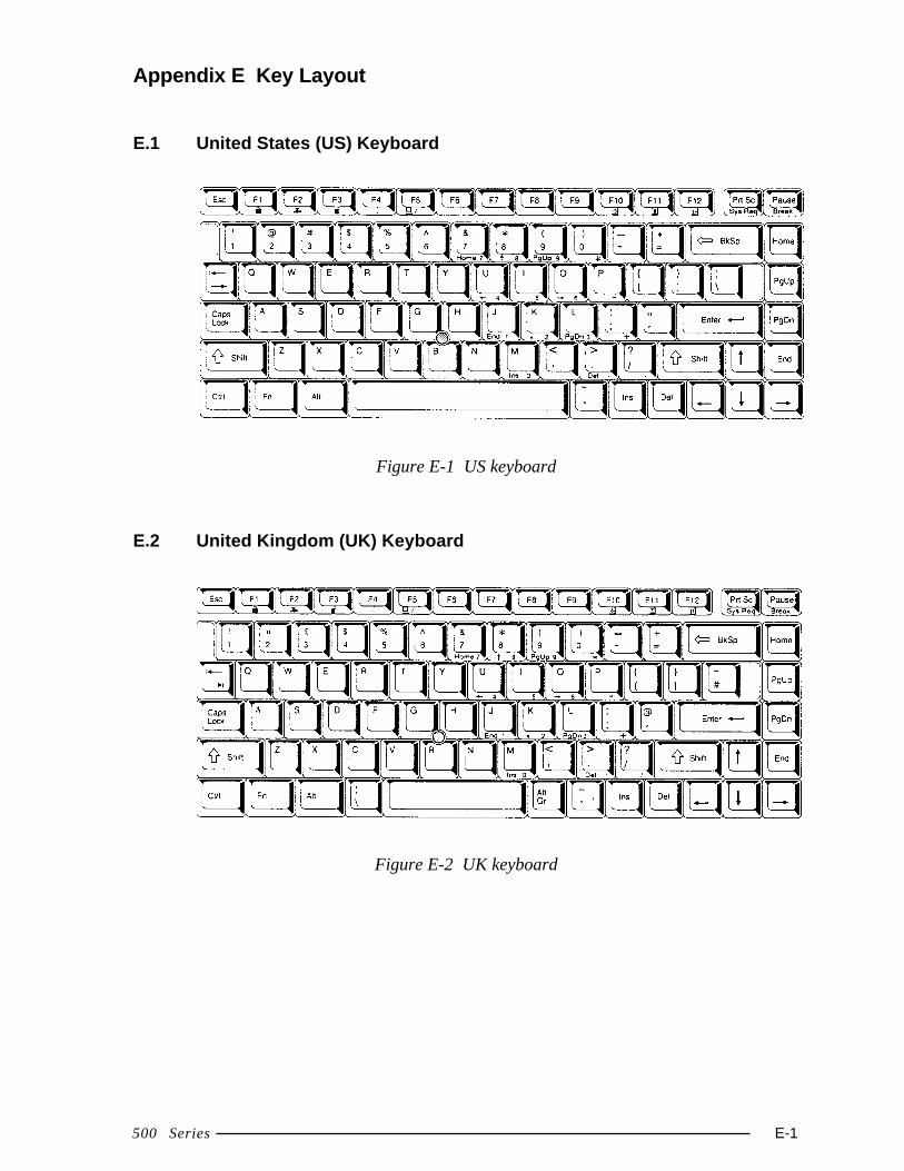
500 Series E-1
Appendix E Key Layout
E.1 United States (US) Keyboard
Figure E-1 US keyboard
E.2 United Kingdom (UK) Keyboard
Figure E-2 UK keyboard
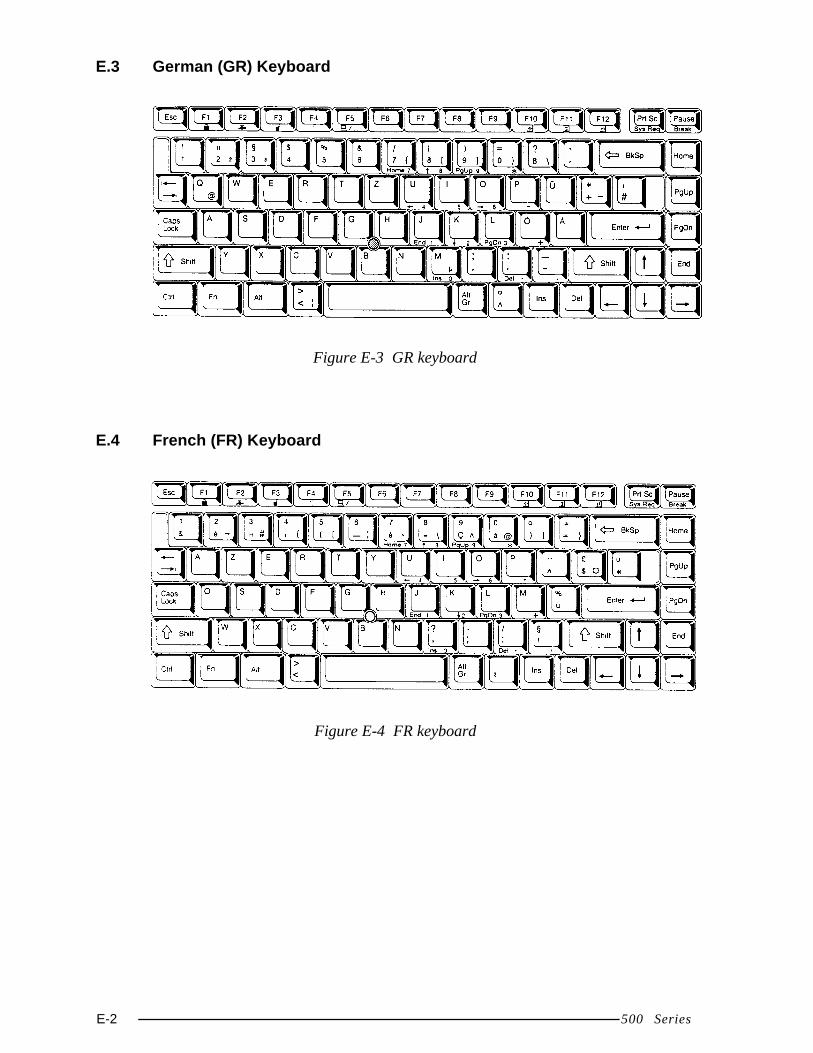
E-2 500 Series
E.3 German (GR) Keyboard
Figure E-3 GR keyboard
E.4 French (FR) Keyboard
Figure E-4 FR keyboard
500 Series E-3
E.5 Spanish (SP) Keyboard
Figure E-5 SP keyboard
E.6 Italian (IT) Keyboard
Figure E-6 IT keyboard

E-4 500 Series
E.7 Scandinavian (SC) Keyboard
Figure E-7 SC keyboard
E.8 Swiss-German (SL) Keyboard
Figure E-8 SL keyboard

500 Series F-1
Appendix F Wiring Diagrams
F.1 Printer Wraparound Connector
(9) +PD7 (15) –ERROR
(8) +PD6 (14) –AUTFD
(7) +PD5 (13) +SELECT
(6) +PD4 (16) –PINIT
(5) +PD3 (1) –STROBE(10) –ACK
(4) +PD2 (12) +PE
(3) +PD1 (17) –SLIN
(2) +PD0 (11) +BUSY
Figure F-1 Printer wraparound connector
F.2 RS-232-C Wraparound Connector
(3) TD (2) RD
(7) RTS (8) CTS(1) CD
(4) DTR (6) DSR(9) RI
Figure F-2 RS-232-C wraparound connector
F.3 RS-232-C Direct Cable (9-Pin to 9-Pin)
(3) TD (2) RD
(4) DTR (6) DSR(8) CTS(9) RI
(7) RTS (1) CD
(5) GND (5) GND
(2) RD (3) TD
(1) CD (7) RTS
(6) DSR (4) DTR(8) CTS(9) RI
Figure F-3 RS-232-C direct cable (9-pin to 9-pin)
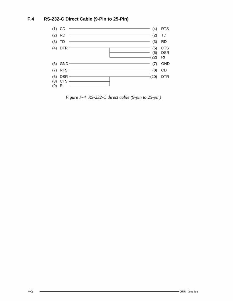
F-2 500 Series
F.4 RS-232-C Direct Cable (9-Pin to 25-Pin)
(1) CD (4) RTS
(2) RD (2) TD
(3) TD (3) RD
(4) DTR (5) CTS(6) DSR
(22) RI
(5) GND (7) GND
(7) RTS (8) CD
(6) DSR (20) DTR(8) CTS(9) RI
Figure F-4 RS-232-C direct cable (9-pin to 25-pin)
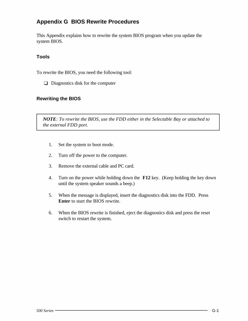
500 Series G-1
Appendix G BIOS Rewrite Procedures
This Appendix explains how to rewrite the system BIOS program when you update thesystem BIOS.
Tools
To rewrite the BIOS, you need the following tool:
❑ Diagnostics disk for the computer
Rewriting the BIOS
NOTE: To rewrite the BIOS, use the FDD either in the Selectable Bay or attached tothe external FDD port.
1. Set the system to boot mode.
2. Turn off the power to the computer.
3. Remove the external cable and PC card.
4. Turn on the power while holding down the F12 key. (Keep holding the key downuntil the system speaker sounds a beep.)
5. When the message is displayed, insert the diagnostics disk into the FDD. PressEnter to start the BIOS rewrite.
6. When the BIOS rewrite is finished, eject the diagnostics disk and press the resetswitch to restart the system.