total ionizing dose test report - infineon technologies · tid test report january 7, 2005 ......
TRANSCRIPT
Total Ionizing DoseTest Report
RDHA720SF06A1NK
January, 2005
International Rectifier RDHA720SF06A1NK TID Test Report January 7, 2005
Table of Contents
I. Introduction ………………………………………………. 3
II. Test Plan ..…………………………………………………. 3
III. Test Results ..……………………………………………... 3 IV. Summary ..…………………………………………………. 6
V. Conclusion ………………………………………………… 6
VI. Figures 1 – 11—Electrical Test ……………………..8 – 13
VII. Figure 12—Bias Conditions ….………….…………..…. 20 Appendix A – Electrical Test Data Appendix B – Test Plan Appendix C – Test Procedure Appendix D – Bias Conditions
International Rectifier RDHA720SF06A1NK TID Test Report January 7, 2005
I. INTRODUCTION
A component-level radiation characterization for Total Ionizing Dose (TID) was performed, from November 2003 to February 2004, for the RDHA720SF06A1NK 60V/20A, single pole, normally open, non-buffered Solid State Relay to determine the total dose tolerance of each component designed into this Solid State Relay. Therefore, this report provides the radiation performance of the RDHA720SF06A1NK, based on analysis of the Isolink Optocoupler OLQ205 (IR Hi-Rel part number C06R015), and the International Rectifier MOSFET IRHC7054 (IR Hi-Rel part number C01R471).
The irradiation was performed at the University of Massachusetts Lowell, Nuclear Research Facility using their Co60 gamma ray source. A total of eight (8) Optocoupler devices, from IMR #012804-013, were irradiated for TID in 25Krad and/or 50Krad intervals, up to a maximum of 250Krads @ a dose rate of 200rads/s(Si); four devices were irradiated under Bias condition A (On) and four devices were irradiated under Bias Condition B (Off). Refer to Figures 1-5 for Optocoupler performance, pre- & post-irradiation. A total of 200 MOSFET die, four (4) from each of fifty (50) wafers, from Wafer Lot EER433690, were irradiated for TID per IR Hi-Rel Test Program T090036G, up to 1000Krads; two (2) die from each wafer were irradiated under VGS Bias Condition (On), (VGS=12V; VDS=0V), and the other two (2) die from each wafer were irradiated under VDS Bias Condition (Off), (VGS=0V; VDS=48V). It should be noted that four (4) wafers from this lot were dispositioned as IRHC7054—100Krad rated die. Therefore, this report will focus on MOSFET performance up to 100Krads. Refer to Figures 6-11 for MOSFET performance, pre- & post-irradiation.
The post-irradiation testing was performed within one hour after the last radiation exposure level was completed. Annealing was not performed on these devices since all devices passed the test conditions and limits provided in the component specification drawings.
II. TEST PLAN
The Test Plan is included in Appendix B. Devices were tested after irradiation as defined by Mil-STD-883, Method 1019. Further details on the test method are explained in Appendix B.
III. RESULTS
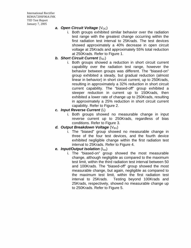
1. Optocoupler A total of eight (8) Optocoupler devices were used for irradiation for TID up to 250Krads—four “biased-on” and four “biased-off”. Refer to the Bias Conditions Section of this report. Five (5) performance characteristics were measured for each Optocoupler for pre-irradiation and post-irradiation, at each radiation exposure level.
International Rectifier RDHA720SF06A1NK TID Test Report January 7, 2005
a. Open Circuit Voltage (VOC) i. Both groups exhibited similar behavior over the radiation
test range with the greatest change occurring within the first radiation test interval to 25Krads. The test devices showed approximately a 40% decrease in open circuit voltage at 25Krads and approximately 55% total reduction at 250Krads. Refer to Figure 1.
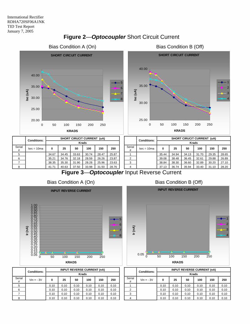
b. Short Circuit Current (ISC) i. Both groups showed a reduction in short circuit current
capability over the radiation test range, however the behavior between groups was different. The “biased-on” group exhibited a steady, but gradual reduction (almost linear in behavior) in short circuit current, up to 250Krads, resulting in approximately a 32% reduction in short circuit current capability. The “biased-off” group exhibited a steeper reduction in current up to 150Krads, then exhibited a lower rate of change up to 250Krads, resulting in approximately a 25% reduction in short circuit current capability. Refer to Figure 2.
c. Input Reverse Current (Ir) i. Both groups showed no measurable change in input
reverse current up to 250Krads, regardless of bias conditions. Refer to Figure 3.
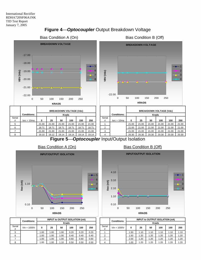
d. Output Breakdown Voltage (VBV) i. The “biased” group showed no measurable change in
three of the four test devices, and the fourth device exhibited negligible change within the first radiation test interval to 25Krads. Refer to Figure 4.
e. Input/Output Isolation (Iiso) i. The “biased-on” group showed the most measurable
change, although negligible as compared to the maximum test limit, within the third radiation test interval between 50 and 100Krads. The “biased-off” group showed the most measurable change, but again, negligible as compared to the maximum test limit, within the first radiation test interval to 25Krads. Testing beyond 100Krads and 25Krads, respectively, showed no measurable change up to 250Krads. Refer to Figure 5.
International Rectifier RDHA720SF06A1NK TID Test Report January 7, 2005
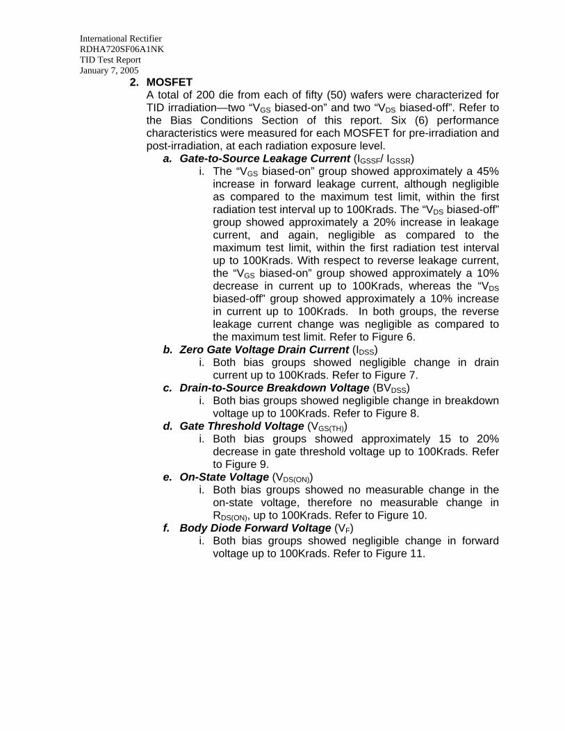
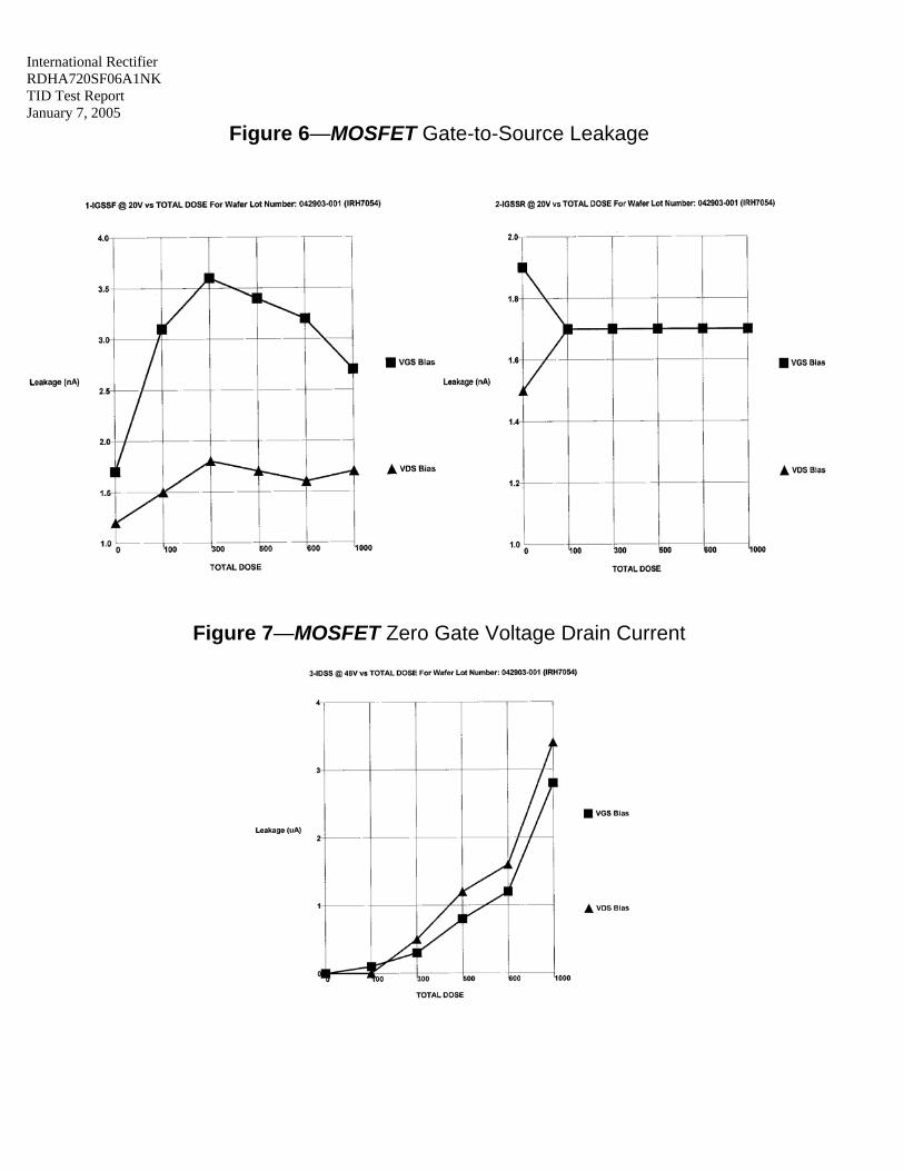
2. MOSFET A total of 200 die from each of fifty (50) wafers were characterized for TID irradiation—two “VGS biased-on” and two “VDS biased-off”. Refer to the Bias Conditions Section of this report. Six (6) performance characteristics were measured for each MOSFET for pre-irradiation and post-irradiation, at each radiation exposure level.
a. Gate-to-Source Leakage Current (IGSSF/ IGSSR) i. The “VGS biased-on” group showed approximately a 45%
increase in forward leakage current, although negligible as compared to the maximum test limit, within the first radiation test interval up to 100Krads. The “VDS biased-off” group showed approximately a 20% increase in leakage current, and again, negligible as compared to the maximum test limit, within the first radiation test interval up to 100Krads. With respect to reverse leakage current, the “VGS biased-on” group showed approximately a 10% decrease in current up to 100Krads, whereas the “VDS biased-off” group showed approximately a 10% increase in current up to 100Krads. In both groups, the reverse leakage current change was negligible as compared to the maximum test limit. Refer to Figure 6.
b. Zero Gate Voltage Drain Current (IDSS) i. Both bias groups showed negligible change in drain
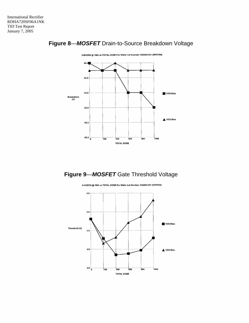
current up to 100Krads. Refer to Figure 7. c. Drain-to-Source Breakdown Voltage (BVDSS)
i. Both bias groups showed negligible change in breakdown voltage up to 100Krads. Refer to Figure 8.
d. Gate Threshold Voltage (VGS(TH)) i. Both bias groups showed approximately 15 to 20%
decrease in gate threshold voltage up to 100Krads. Refer to Figure 9.
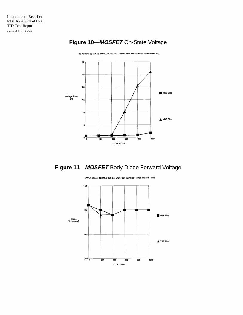
e. On-State Voltage (VDS(ON)) i. Both bias groups showed no measurable change in the
on-state voltage, therefore no measurable change in RDS(ON), up to 100Krads. Refer to Figure 10.
f. Body Diode Forward Voltage (VF) i. Both bias groups showed negligible change in forward
voltage up to 100Krads. Refer to Figure 11.
International Rectifier RDHA720SF06A1NK TID Test Report January 7, 2005 IV. SUMMARY
The RDHA720SF06A1NK 60V/20A is designed to be a Radiation Hardened, single pole, normally open, non-buffered Solid State Relay consisting of two part types—two (2) each of Isolink Optocoupler OLQ205 (IR Hi-Rel part number C060015), and one (1) each of International Rectifier MOSFET IRHC7054 (IR Hi-Rel part number C01R471). The Optocoupler outputs are configured in parallel for higher gate drive capability. To demonstrate radiation hardness, the Optocoupler and MOSFET were irradiated for TID up to and thru 100Krads, the radiation hardness specified for the RDHA720SF06A1NK Solid State Relay. The data up to 100Krads, contained within, shows that while certain characteristics or parameters of the Optocoupler and MOSFET have degraded, the irradiated components continue to meet the component specification requirements.
V. CONCLUSION
The RDHA720SF06A1NK Solid State Relay is comprised of two (2) Isolink OLQ205 Optocouplers and one (1) International Rectifier, all housed in a hermetic 5-pin Single In-line Package (SIP). Both the Optocoupler and the MOSFET have been characterized for TID radiation levels up to and including 100Krads, and both components have demonstrated a strong degree of hardness to TID radiation of 100Krads. Devices irradiated in the “biased-on” groups showed the most change when exposed to ionizing irradiation; however, all parameters passed their post-irradiation test specifications and limits. Therefore, based on the analyses contained within for the OLQ205 Optocoupler and the IRHC7054 MOSFET, the combination and integration of these components make the RDHA720SF06A1NK Solid State Relay usable in applications where it is subjected to Gamma radiations up to 100Krads.

International Rectifier RDHA720SF06A1NK TID Test Report January 7, 2005
Appendix A
Electrical Test Data

International Rectifier RDHA720SF06A1NK TID Test Report January 7, 2005
Figure 1—Optocoupler Open Circuit Voltage
Bias Condition A (On) Bias Condition B (Off)
OPEN CIRCUIT VOLTAGE
8.509.50
10.5011.5012.5013.5014.5015.5016.5017.5018.5019.50
0 50 100 150 200 250
KRADS
Voc
(Vdc
)
5
6
7
8
OPEN CIRCUIT VOLTAGE
8.509.50
10.5011.5012.5013.5014.5015.5016.5017.5018.5019.50
0 50 100 150 200 250
KRADS
Voc
(Vdc
)
1
2
3
4
OPEN CIRCUIT VOLTAGE (Vdc) OPEN CIRCUIT VOLTAGE (Vdc)
Conditions:
Krads Conditions:
Krads Serial
# Isrc = 10ma,
Vin = 0 25 50 100 150 250
Serial #
Isrc = 10ma, Vin = 0 25 50 100 150 250
5 2.66 19.39 11.76 11.17 10.62 10.50 9.94 1 2.66 19.42 11.85 11.29 10.76 10.52 10.01 6 2.67 19.36 11.62 10.95 10.41 10.24 9.72 2 2.65 19.37 11.75 11.15 10.61 10.39 9.89 7 2.67 19.32 11.65 11.01 10.43 10.28 9.76 3 2.66 19.44 11.66 11.16 10.60 10.37 9.86 8 2.66 19.40 11.93 11.31 10.75 10.59 10.09 4 2.67 19.40 11.97 11.41 10.88 10.65 10.14
International Rectifier RDHA720SF06A1NK TID Test Report January 7, 2005
Figure 2—Optocoupler Short Circuit Current
Bias Condition A (On) Bias Condition B (Off)
SHORT CIRCUIT CURRENT
20.00
25.00
30.00
35.00
40.00
0 50 100 150 200 250
KRADS
Isc
(uA
)
5
6
7
8
SHORT CIRCUIT CURRENT
25.00
30.00
35.00
40.00
0 50 100 150 200 250
KRADSIs
c (u
A)
1
2
3
4
SHORT CIRUCIT CURRENT (uA) SHORT CIRUCIT CURRENT (uA)
Conditions:
Krads Conditions:
Krads Serial
# Isrc = 10ma 0 25 50 100 150 250 Serial
# Isrc = 10ma 0 25 50 100 150 250
5 34.67 34.45 33.63 30.74 28.47 25.87 1 35.44 34.94 34.13 31.70 29.35 28.65 6 35.21 34.76 32.18 28.59 26.26 23.87 2 39.08 38.48 36.45 32.61 29.88 26.89 7 38.35 35.30 31.90 28.28 25.96 23.63 3 38.84 38.30 36.60 32.89 30.20 27.10 8 41.71 40.63 37.50 33.98 31.50 28.76 4 37.13 36.74 35.94 33.40 31.10 28.20
Figure 3—Optocoupler Input Reverse Current
Bias Condition A (On) Bias Condition B (Off)
INPUT REVERSE CURRENT
0.050.100.150.200.250.300.350.400.450.500.550.600.650.700.750.800.850.900.951.00
0 50 100 150 200 250
KRADS
Ir (n
A)
5
6
7
8
INPUT REVERSE CURRENT
0.05 0 50 100 150 200 250
KRADS
Ir (n
A)
1
2
3
4
INPUT REVERSE CURRENT (nA) INPUT REVERSE CURRENT (nA)
Conditions:
Krads Conditions:
Krads Serial
# Vin = - 3V 0 25 50 100 150 250 Serial
# Vin = - 3V 0 25 50 100 150 250
5 0.10 0.10 0.10 0.10 0.10 0.10 1 0.10 0.10 0.10 0.10 0.10 0.10 6 0.10 0.10 0.10 0.10 0.10 0.10 2 0.10 0.10 0.10 0.10 0.10 0.10 7 0.10 0.10 0.10 0.10 0.10 0.10 3 0.10 0.10 0.10 0.10 0.10 0.10 8
0.10 0.10 0.10 0.10 0.10 0.10 4
0.10 0.10 0.10 0.10 0.10 0.10
International Rectifier RDHA720SF06A1NK TID Test Report January 7, 2005
Figure 4—Optocoupler Output Breakdown Voltage
Bias Condition A (On) Bias Condition B (Off)
BREAKDOWN VOLTAGE
-22.00
-21.00
-20.00
-19.00
-18.00
-17.00
0 50 100 150 200 250
KRADS
VBV
(Vdc
)
5
6
7
8
BREAKDOWN VOLTAGE
-22.000 50 100 150 200 250
KRADSVB
V (V
dc)
1
2
3
4
BREAKDOWN VOLTAGE (Vdc) BREAKDOWN VOLTAGE (Vdc)
Conditions: Krads Conditions: Krads Serial
# Isrc = 10ma 0 25 50 100 150 250 Serial
# Isrc = 10ma 0 25 50 100 150 250 5 21.00 21.00 21.00 21.00 21.00 21.00 1 21.00 21.00 21.00 21.00 21.00 21.00 6 18.71 18.71 18.71 18.71 18.71 18.71 2 21.00 21.00 21.00 21.00 21.00 21.00 7 21.00 21.00 21.00 21.00 21.00 21.00 3 21.00 21.00 21.00 21.00 21.00 21.00 8 19.10 19.12 19.14 19.14 19.14 19.14 4 20.30 20.30 20.30 20.30 20.30 20.30
Figure 5—Optocoupler Input/Output Isolation
Bias Condition A (On) Bias Condition B (Off)
INPUT/OUTPUT ISOLATION
0.10
1.10
2.10
3.10
4.10
0 50 100 150 200 250
KRADS
Iiso
(nA
)
1
2
3
4
INPUT/OUTPUT ISOLATION
0.10
1.10
0 50 100 150 200 250
KRADS
Iiso
(nA
)
5
6
7
8
INPUT to OUTPUT ISOLATION (nA) INPUT to OUTPUT ISOLATION (nA)
Conditions:
Krads Conditions:
Krads Serial
# Vin = 1000V 0 25 50 100 150 250 Serial
# Vin = 1000V 0 25 50 100 150 250
5 1.00 1.00 1.00 0.20 0.20 0.20 1 1.50 1.10 1.10 1.10 1.10 1.10 6 1.00 1.00 1.00 0.40 0.40 0.40 2 1.50 1.20 1.20 1.20 1.20 1.20 7 1.00 1.00 1.00 0.60 0.60 0.60 3 2.00 1.20 1.20 1.20 1.20 1.20 8 1.00 1.00 1.10 0.50 0.50 0.50 4 1.00 1.20 1.20 1.20 1.20 1.20
International Rectifier RDHA720SF06A1NK TID Test Report January 7, 2005
Figure 6—MOSFET Gate-to-Source Leakage
Figure 7—MOSFET Zero Gate Voltage Drain Current
International Rectifier RDHA720SF06A1NK TID Test Report January 7, 2005
Figure 8—MOSFET Drain-to-Source Breakdown Voltage
Figure 9—MOSFET Gate Threshold Voltage
International Rectifier RDHA720SF06A1NK TID Test Report January 7, 2005
Figure 10—MOSFET On-State Voltage
Figure 11—MOSFET Body Diode Forward Voltage
International Rectifier RDHA720SF06A1NK TID Test Report January 7, 2005
Appendix B
Test Plan

International Rectifier RDHA720SF06A1NK TID Test Report January 7, 2005
1. Purpose The purpose of this test is to characterize and qualify this device for TID effects for International Rectifier’s hybrid SSR devices. The data resulting from the tests shall be incorporated into the IR data sheet.
2. Test Responsibility International Rectifier shall be responsible for conducting the tests, which shall be performed at the University of Massachusetts Research Reactor (UMRR) Facility. International Rectifier shall be responsible for the final Test Report.
3. Test Facility a. Nuclear Reactor—The University of Massachusetts Research Reactor (UMRR)
shall be used to provide the source for Gamma radiation. UMRR will also provide information on dose rate, total dose, irradiation test times and dosimetry for this evaluation.
b. Test Equipment--The necessary test equipment including interface board, cables, power supplies, measurement system, etc. shall be provided by International Rectifier.
c. Sample Size—Sample size shall be determined based on device type and characterization parameters. As a minimum, the sample size shall meet the requirements of Mil- PRF-38534.
4. Test Devices
a. Element Evaluation components are planned for TID characterization and evaluation.
b. All devices shall be built in packages as defined in the component-level drawings. c. Devices shall be properly sealed and packed in static-free containers. d. All devices shall be verified for correct electrical performance (baseline) prior to
arrival at UMRR.
5. Test Method Mil- PRF-38534 shall be used to establish procedure for all testing described herein. See Appendix C, Test Procedure.
6. Record Keeping The Reactor facility shall provide dosimetry data for the Cobalt60. Each exposure run shall be cataloged with the appropriate lot number and group letter in order to maintain correlation to the appropriate data set. IR will be responsible for collecting and compiling the test data.
7. Test Report The Test Report shall include the following information:
a. Device type(s), serial numbers, lot identification (per active component) b. Facility and radiation source type c. Schematic of test circuit and bias conditions d. Electrical Test Data e. Descriptive Summary including graphs (if applicable)

International Rectifier RDHA720SF06A1NK TID Test Report January 7, 2005
Appendix C
Test Procedure
International Rectifier RDHA720SF06A1NK TID Test Report January 7, 2005
1. Preliminary Setup a. Perform baseline testing on each device prior to irradiation. The Optocoupler
devices shall be tested per Manual Test Procedure T031104X and the MOSFET devices shall be tested per Radiation Test Program T090036G and Electrical Test Specification T052113G. Remove any device that fails pre-radiation test limits and replace with a known good unit.
b. Divide the selected Optocoupler devices into two groups. Each group shall contain 4 devices. One group will be used for Bias Condition A (On) and the other group for Bias Condition B (Off).
c. Prepare the MOSFETs for irradiation per Radiation Test procedure T030043G. d. Prepare devices for transportation to the Radiation facility. Devices must be stored
in a static free container. Device pins must be shorted.
2. Test Equipment a. Keithley Source Meter—Model 2410 b. Optocoupler Test Board—TF-04-017 c. MOSFET Test Board—TF-04-145 d. 15ft Power Supply Cable (1 ea) e. Radiation Test Power Supply Rack—PC-02-001
3. Radiation Setup
Note: Refer to Total Dose Radiation Test Procedure T030043G for MOSFET Irradiation. a. Prepare the QF299 form with the appropriate information re: Part Type,
Description, Part No, etc. b. Select control devices, if applicable, and record their serial numbers on the
QF299 form as control units. c. Record device serial numbers, targeted for irradiation, on the QF299
form as “biased” and “un-biased” units. Load the Test Board (TF-xx-xxx) sockets designated “biased on” and “biased off”, as applicable.
d. Move the test board into the Gamma room and insert into the irradiation fixture. e. In the test room, connect the Keithley 2410 source meter to the Voltage Input source
connector on the power supply rack. f. Adjust the Voltage Input Keithley for “constant current” mode. Set the voltage level
to 5.0 volts and the current to 40ma (10mA per Bias Condition A (On) device). g. Enable the output of the Keithley. h. Measure the input and output voltage on each socket on the test board.
Note: If voltage is out of tolerance, correct the problem and retest. i. Secure the Gamma room and notify reactor personnel to place the
Cobalt60 source on the rack. Note: Record the time the Cobalt60 source is in place on the QF299 form.

International Rectifier RDHA720SF06A1NK TID Test Report January 7, 2005
j. When the exposure run is complete, record the time on the QF299 form. k. Disable the output of the Keithley. l. Remove the test board from the Gamma room and return to the test room. m. Radiation exposure is complete.
4. Return to IR Facility
a. Place devices into a static free container. Maintain an ambient Temperature of 25°C or less.

International Rectifier RDHA720SF06A1NK TID Test Report January 7, 2005
Appendix D
Bias Conditions
International Rectifier RDHA720SF06A1NK TID Test Report January 7, 2005
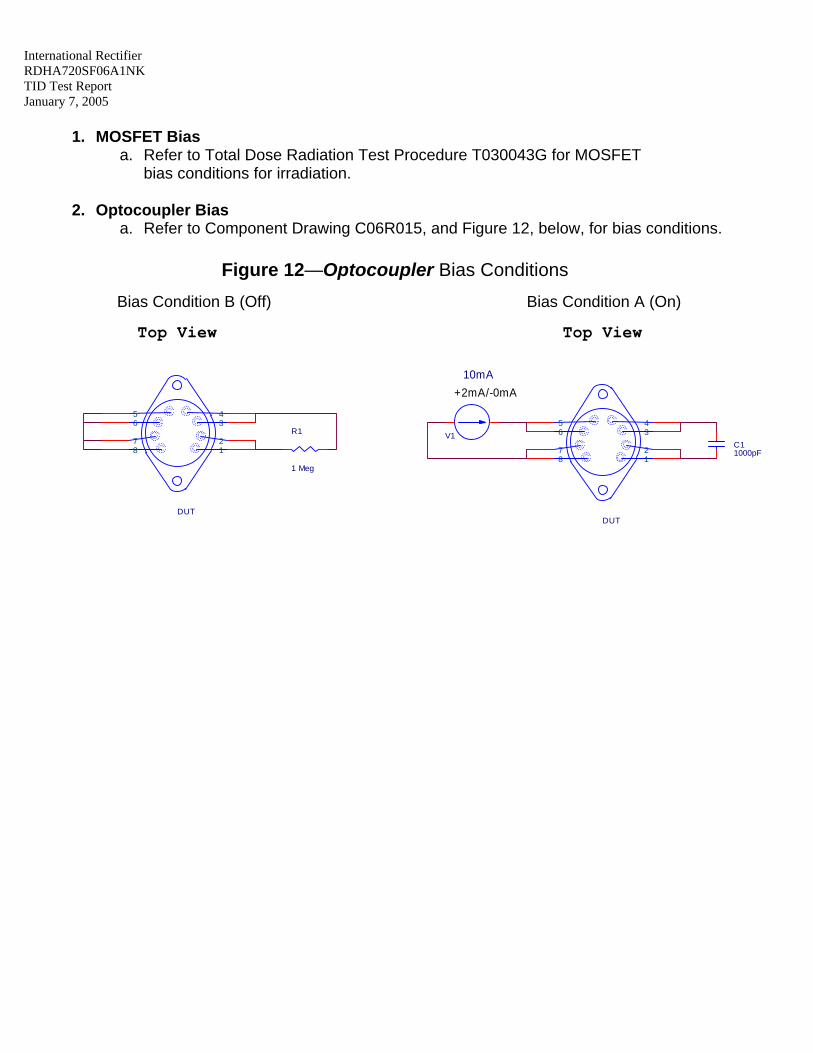
1. MOSFET Bias a. Refer to Total Dose Radiation Test Procedure T030043G for MOSFET
bias conditions for irradiation.
2. Optocoupler Bias a. Refer to Component Drawing C06R015, and Figure 12, below, for bias conditions.
Figure 12—Optocoupler Bias Conditions
Bias Condition B (Off) Bias Condition A (On)
Top View
C11000pF
Top View
R1
1 Meg
V1
10mA+2mA/-0mA
DUT
12
345
6
78
DUT
12
345
6
78