towards the formal verification of the requirements … contractor report 4522 towards the formal...
TRANSCRIPT

NASA Contractor Report 4522
Towards the Formal Verification
of the Requirements and Design
of a Processor Interface Unit
David A. Fura
The Boeing Company
Seattle, Washington
Phillip J. Windley
University of Idaho
Moscow, Idaho
Gerald C. Cohen
The Boeing Company
Seattle, Washington
Prepared for
Langley Research Center
under Contract NAS1-18586
National Aeronautics andSpace Administration
Office of Management
Scientific and TechnicalInformation Program
1993
ur_p..o,,I"NI
,4"O_Z
ul_0
U
LUu
C_ ZUU Uu.. uJ I.- _
_rz O._.j ij.jb,=4_"p
,...o_-"Yc,'__o _t4_
3c L,UO _
¢,
NZO I_ I_
d.O r_
,.....,> ,,4 _ L-_
_t0um0
N0
N_0
I"
https://ntrs.nasa.gov/search.jsp?R=19940019602 2018-05-31T02:12:44+00:00Z


Preface
This document was generated in support of NASA contract NAS 1-18586, Design and Validation of Digital
Flight Control Systems Suitable for Fly-By-Wire Applications, Task Assignment 10. Task 10 is concernedwith the formal specification and verification of a processor interface unit.
This report describes the formal verification of the design and partial requirements for a processor interface
unit using the HOL theorem-proving system. The HOL listings from the formal verification are documentedin NASA CR- 191466. The processor interface unit is a single-chip subsystem within a fault-tolerant embed-
ded system under development within the Boeing Defense & Space Group. It provides the opportunity to
investigate the specification and verification of a real-world subsystem within a commercially-developed
fault-tolerant computer.
The NASA technical monitor for this work is Sally Johnson of the NASA Langley Research Center, Hamp-
ton, Virginia.
The work was accomplished at the Boeing Company, Seattle, Washington and the University of Idaho,
Moscow, Idaho. Personnel responsible for the work include:
Boeing Defense & Space Group:
Dagfinn Gangsaas, Responsible ManagerThomas M. Richardson, Program Manager
Gerald C. Cohen, Principal Investigator
David A. Fura, Researcher
University of Idaho:
Dr. Phillip J. Windley, Chief Researcher
o°o
111
I:K rtS_i:


Contents
Introduction ............................................................................................................................................
1.1 Informal PIU Description .............................................................................................................
1.2
1
2
1.1.1 PMM Initialization ............................................................................................................ 4
1.1.2 CPU Accesses to Memory ................................................................................................ 4
1.1.2.1 Accessing Local Memory ................................................................................. 4
1.1.2.2 Accessing the Internal Register File .................................................................. 5
1.1.2.3 Accessing the the C_Bus ................................................................................... 6
1.1.3 C_Bus Accesses to Memory ............................................................................................. 6
1.1.4 Timers and Interrupts ........................................................................................................ 7
Specification Overview ................................................................................................................. 7
Processor Port Description ..................................................................................................................... 9
2.1 P_Port Operation Overview .......................................................................................................... 92.2 HOL Variables ............................................................................................................................ 13
PIU Design Verification ...................................................................................................................... 15
3.1 Overall Approach ....................................................................................................................... 153.2 Standard Cases ............................................................................................................................ 16
3.3 The Harder Cases ........................................................................................................................ 18
3.3.1 Non-standard Array Accesses ......................................................................................... 183.3.2 Tri-State Buses ................................................................................................................ 19
3.4 Discussion ................................................................................................................................... 19
3.4.1
3.4.2
3.4.3
Generation of Gate-Level Models .................................................................................. 20
Generation and Verification of Clock-Level Models ..................................................... 20
Bus Modules ................................................................................................................... 21
4 PIU Requirements Verification ........................................................................................................... 23
4.1 P_Port Description ...................................................................................................................... 23
4.1.1 Signals ............................................................................................................................. 23
4.1.2 Significant Event Times .................................................................................................. 24
4.2 Overall Verification Approach ................................................................................................... 254.2.1 Transaction-Level Interpreter ......................................................................................... 25
4.2.1.1 Execution Predicate ......................................................................................... 26
4.2.1.2 Precondition ..................................................................................................... 26
4.2.1.3 Postcondition .................................................................................................... 27
4.2.2 Abstraction Predicate ...................................................................................................... 27
4.2.3 Theorem Proving with the Pre-Post Interpreter Model .................................................. 284.3 Transaction Address Verification ............................................................................................... 29
4.3.1 Top Level Proof Steps .................................................................................................... 324.3.1.1 Flowthru Case .................................................................................................. 34
4.3.1.2 Delayed Case ................................................................................................... 344.3.2 Relating the L_Bus and I_Bus Transaction Times ......................................................... 34
4.3.2.1 The Transaction 'Onto' Relationship .............................................................. 354.3.2.2 The Transaction 'One-to-One' and 'Causality' Relationships ........................ 36
4.3.2.3 Discussion ........................................................................................................ 36
4.3.3 Theorem Proving Over Intervals .................................................................................... 374.4 Transaction Block-Size Verification .......................................................................................... 38
, ' r . :'._ W
PII__ PA(_E _L_[_-iK NOT F|LMEL_

4.5 Discussion..................................................................................................................................414.5.1 CurrentStatus.................................................................................................................414.5.2 TheTransaction-LevelVerificationProcess..................................................................41
Conclusions..........................................................................................................................................435.1 Clock-LevelVerification............................................................................................................435.2 Transaction-LevelVerification...................................................................................................435.3 DesignIssues..............................................................................................................................445.4 FutureWork................................................................................................................................44
6 References............................................................................................................................................46
A HOLOverview....................................................................................................................................47A.1 TheLanguage............................................................................................................................47A.2 TheProofSystem.......................................................................................................................49
vi

List of Figures
1.1 Block Diagram of the Processor-Memory Module (PMM) ......................................................... 2
1.2 Major Blocks of the Processor Interface Unit (PIU) .................................................................... 3
1.3 PIU Specification Hierarchy for the P Process .......................................................................... 7
2.1 Circuit Diagram for the PIU Processor Port (P_Port) ................................................................ 10
2.2 P_Port FSM Description ............................................................................................................. 11
3.1 Correspondence Between an Example Structure and its Behavioral Definition ........................ 20
3.2 Example Bus Module and its Gate-Level Definition ................................................................. 21
4.1 Significant Events and Times Within a P_Port Transaction ...................................................... 244.2 Transaction One-to-One and Onto Relationships ....................................................................... 35
4.3 Informal and HOL Definitions for the Transaction Block Size ................................................. 39
vii


List of Tables
1.1 R_Port Register Definitions .......................................................................................................... 6
2.1 P_Port HOL Variables and Their Types ..................................................................................... 13
4.1 Major Theorems of the Transaction Address Proof ................................................................... 294.2 Lemmas Used in the Top-Level Address Proof ......................................................................... 33
4.3 Major Theorems Used in the First Block-Size Proof ................................................................. 40
A.I HOL Infix Operators .................................................................................................................. 48A.2 HOL Binders .............................................................................................................................. 48
A.3 HOL Type Operators ................................................................................................................. 49
I:,I_{wg._D_N@PAGE _LA{_K NOT FILMED
,_:__:. _B_ " ' : ix


1 Introduction
This report describes work to formally verify the requirements and design of a processor interface unit
(PIU), a single-chip subsystem providing memory-interface, bus-interface, and additional support services
for a commercial microprocessor within a fault-tolerant computer system. This system, the Fault-Tolerant
Embedded Processor (FTEP), is targeted towards applications in avionics and space requiting extremely
high levels of mission reliability, extended maintenance-free operation, or both. Since the need for high-
quality design assurance in such systems is an undisputed fact, the continued development and application
of formal methods is vital as these systems see increasing use in modern society.
The work described in this report represents part of our early progress in developing a provably correct
fault-tolerant computing platform for application to real commercial, military, and spaceborne systems. It
thus represents a transfer of formal modeling and verification methods from academic settings into 'real-
world' hardware applications. The test case for our initial attempt at this - the PIU - has an'ned out to be a
good choice in that it exploits recent academic research developed, in part, under this contract. It has also
helped to focus new research towards the important problems affecting real-world hardware modeling and
verification.
This report is one of two describing the results of Task 10 of a multi-year NASA contract. The other
report, which we will sometimes refer to as the 'Specification Report,' describes work to formally specify
the PIU design and requirements [Fur93a]. Two additional reports contain the actual HOL listings of the
formal specification and verification [Fur93b][Fur93c]. All specification and verification work was per-
formed using the HOL theorem proving system from the University of Cambridge IGor88].The research focus of Task 10 was on abstraction. One of the major accomplishments of this work is a
new approach for modeling PIU requirements, and the successful specification and verification of a non-
trivial subset of these requirements using this model. The model was also used to specify and verify the PIU
design (or implementation).A secondary emphasis of the Task 10 work was composition; an issue that gained in importance as this
work progressed. We have identified an approach to achieve secure composition of PIU ports, as well as the
PIU itself, at high levels of abstraction [Fur93a].
The verification described in this report exploits the research developed in earlier tasks of this contract.
Specifically, the design verification described in Section 3 employs the hierarchical specification methods,
described in [Win90], to greatly reduce the verification burden there.
Unfortunately, the current state-of-the-art in requirements verification lags considerably behind that of
lower-level design verification. We are aware of no chip as complicated as the PIU being formally specified,
let alone verified, at a level of abstraction corresponding to the PIU transaction level. As explained in Sec-
tion 4, the lack of prior experience on verifications of this type has forced us to perform a considerable
amount of +seat-of-the-pants' theorem proving. Already we have gained significant insight into how future
verifications can be structured to ease the burden on the verifier, however much work remains to be done to
make requirements verification anywhere near as straightforward as design verification.
This report is divided into four sections following this introduction. Section 2 describes the Processor
Port of the PIU in some detail to support the discussions of the PIU design verification (in Section 3) and
the partial requirements verification (in Section 4). Section 5 contains our conclusions. A brief description
of the HOL theorem-proving system is provided in Appendix A.
Before leaving this section, we present an informal description of the PIU, including both its structure
and an overview of its behavior. Following this we introduce the specification hierarchy developed for the
PIU.

1.1 Informal PIU Description
The PIU is a single-chip subsystem providing memory-interface, bus-interface, and additional support
services within the Processor-Memory Module (PMM) of the F'IEP system. The PIU's position within the
PMM structure is shown in Figure 1.1. A PMM, itself a single block within an FTEP Core, interconnects
three internal PMM subsystems: the local processors, the local memory, and the Core Bus (C_Bus) inter-face.
The PMM processors (CPU0 and CPU1) are arranged in a cold-sparing configuration to enhance long-
life operation. Only one processor is active during a given mission. The choice of active processor is deter-
mined during initialization. The spare processor is disabled by the PIU through assertion of the processor's
cpu_reset input. For the first implementation of the PMM, described in this report, lntel 80960MC micro-
processors [Int89] are used for the local processors. They communicate with the PIU using the L_Bus busprotocol of the 80960.
Processor programs and data are stored in local electrically-erasable programmable read-only memory
(EEPROM) and static random access memory (SRAM), respectively. Memory accesses are initiated by
either the local processor or an external block acting as C_Bus master. In either case the PIU provides the
memory interface. The features provided by the PIU include memory error correction, memory locking to
implement atomic read-modify-write operations, byte accesses, and block accesses of up to 64 words.
EEPROM and SRAM memory capacity in the first implementation is 1 MB (megabyte) of actual informa-
tion storage each, implemented within seven 256Kx8-bit memory chips each. A (7,4) Hamming code pro-vides single-bit error correction on memory reads.
The PIU also provides processor support features such as timers and interrupt control. Two M-bit timers
can be set by the processor to provide either timekeeping or watchdog functions. Processor interrupts are
SRAM
EEPROM
M_Bus
prom_resetpiu_clkcbus_clk
t ii iiiiiii iiiiJ
cpuO_reset J
failureO_ _ CPUO
• /
-failure 1 | CPU 1
!Core Bus Interface
Figure 1.1: Block Diagram of the Processor-Memory Module (PMM).
2

generatedwithinthePIUundertwoconditions.Oneconditionisatimertime-out;theotherisawriteoper-ationto aspeciallydesignatedPIUregisterbyeitherthelocalprocessororC_Busmaster.
Theresetandclocksignalsat thetopof Figure1.1areproducedby theFault-TolerantClockUnit(FTCU)notshownhere.Theprom_reset signal is sent only to the PIU to allow it greater control over the
local processors. For example, the PIU uses this signal to enter its initialization mode, during which it acti-
vates the processor reset signals. All of the PIU input signals produced by the FI'CU are synchronized with
those in the PlUs in redundant PMMs of a fault-tolerant FTEP core.
The structure of the PIU itself is shown in Figure 1.2. The Processor Port (P_Port), C_Bus Port
(C_Port), and Memory Port (M_Port) implement the communication protocols for the L_Bus, C_Bus, and
M_Bus, respectively. The M_Port also implements (7,4) Hamming encoding and decoding on writes and
reads, respectively, to the local memory, and the C_Port implements single-bit parity encoding and decoding
for C_Bus transfers.
The Register Port (R_Port) is the fourth, and final, port residing on the PIU's Internal Bus (I_Bus). It
contains a state machine, counters, and various command and status registers used by the local processor to
implement timers and interrupts.
M Bus
f
_ _ I_BusM_Port
piu_clk prom_resetcbus_clk
R_Port SU_Cont
resets &disables
P_Port
C_Port
C_Bus
J
intl 3.'O]
cpuO_resetcpul_reset
failureO_failure l_
L_Bus
Figure 1.2: Major Blocks of the Processor Interface Unit (PIU).

TheStart-up Controller (SU_Cont) implements the PMM initialization sequence. After it has concluded
initialization, control is turned over to the other ports with the SU_Cont continuing operation in a back-
ground mode. The SU_Cont is not physically located on the I_Bus; however, for convenience, we will
sometimes refer to it as one of the five PIUports.
Behaviorally, the PIU functionality can be divided into four categories: (1) PMM initialization, (2)
local-processor memory accesses, (3) C_Bus memory accesses, and (4) timers and interrupts.
1.1.1 PMM Initialization
The PIU controls the PMM initialization sequence. After receiving a synchronous pmm_reset signal
from the PTCU, the PIU initiates the testing of the two local processors (or CPUs). Based on the test results,
the PIU selects one of the CPUs to be active for the upcoming mission, while at the same time isolating the
other CPU. During the initialization, the PIU also maintains the inter-PMM synchronization that is initially
established by the FTCUs.
The PIU initiates CPU self-test via the CPU reset signals that it controls. To begin the initialization
sequence, the PIU resets CPU0, which then goes through a two-phase (Intel 80960) testing process of its
own. In the first phase the CPU executes a 47,000-cycle self-test procedure; in the second phase the CPU
reads the first eight words of local memory (via the PIU) and performs a check-sum test. If either of these
tests fail, then the CPU'sfailureO_ pin remains asserted, otherwise it is deasserted.
After the CPU self-test is completed, the CPU executes a software-based test using a program and the
prior-mission fault status stored in local memory. At preselected points in this program the CPU updates
PIU registers in a prespecified manner. At the end of this program, the PIU compares the modified PIU reg-
ister values against their expected values. This acceptance test is the final major test of CPU functionalityduring initialization.
At the same time that CPU0 is being tested, the PIU isolates CPU1 by asserting its cpul_reset input.
Once the testing of CPU0 is completed, the roles are reversed. After both CPUs have been tested, the PIU
selects one to be active for the upcoming mission. The selection algorithm makes use of the CPU failure
signal outputs and the acceptance-test results: if CPU0 is ok then it is selected, otherwise if CPU 1 is ok then
it is selected, otherwise neither one is selected. Once the choice is made, the selected CPU is reset again and
begins normal operation. The PIU isolates the other CPU by keeping its reset active.
An important PIU requirement is to maintain clock-level synchronization between redundant PMMs,
yet accommodate possible nondeterminism within the PMM initialization sequences. Before the PMM ini-
tialization begins, the redundant PMM clocks are synchronized by the FTCUs, and pmm_reset signals are
delivered to the PIUs synchronously across all PMMs. Synchronization is maintained by establishing max-
imum time durations for each phase of the initialization and having each PMM use the entire duration. The
PIUs enforce these phase boundaries and thus guarantee that each PMM leaves its initialization on precisely
the same clock cycle.
1.1.2 CPU Accesses to Memory
The PIU controls CPU reads and writes to the local memory, the internal PIU registers, and global mem-
ory.
1.1.2.1 Accessing Local Memory
The PIU implements error-correction code (ECC) encoding and decoding and supports atomic memory
operations, byte accesses, and 2-, 3-, and 4-word block transfers.
4
Onwritesto thelocalmemory,thePIUencodesthe32-bitdatawordsusinga single-error-correction(7,4)Hammingcode.The56-bitencodedwordsarestoredsuchthateach7-bitword(thereareeightofthese)isspreadamongtheseven256Kx8-bitmemorychips.Onreads,thedecodingprocessimplementedwithinthePIUmasksall faultsaffectingoneof thesevenbitsof eachcodeword.Entirememory-chipfail-uresarethushandled.
Atomicmemoryaccesses,the'atomicadd'and'atomicmodify'instructionsof thelntel80960instruc-tionset,aresupportedbythePIU.DuringtheseoperationsthePIUpreventstheC_Busfromgainingaccesstothelocalmemory.ThePIUusesthelock_ signal provided by the CPU during these operations.
Byte accesses to the local memory are supported by the PIU. Reads are implemented in a straightfor-
ward way. Writes are implemented using a read-modify-write operation that reencodes the entire 32-bit data
word.
Byte accesses of up to four words are also supported to implement cache refilling within the CPU.
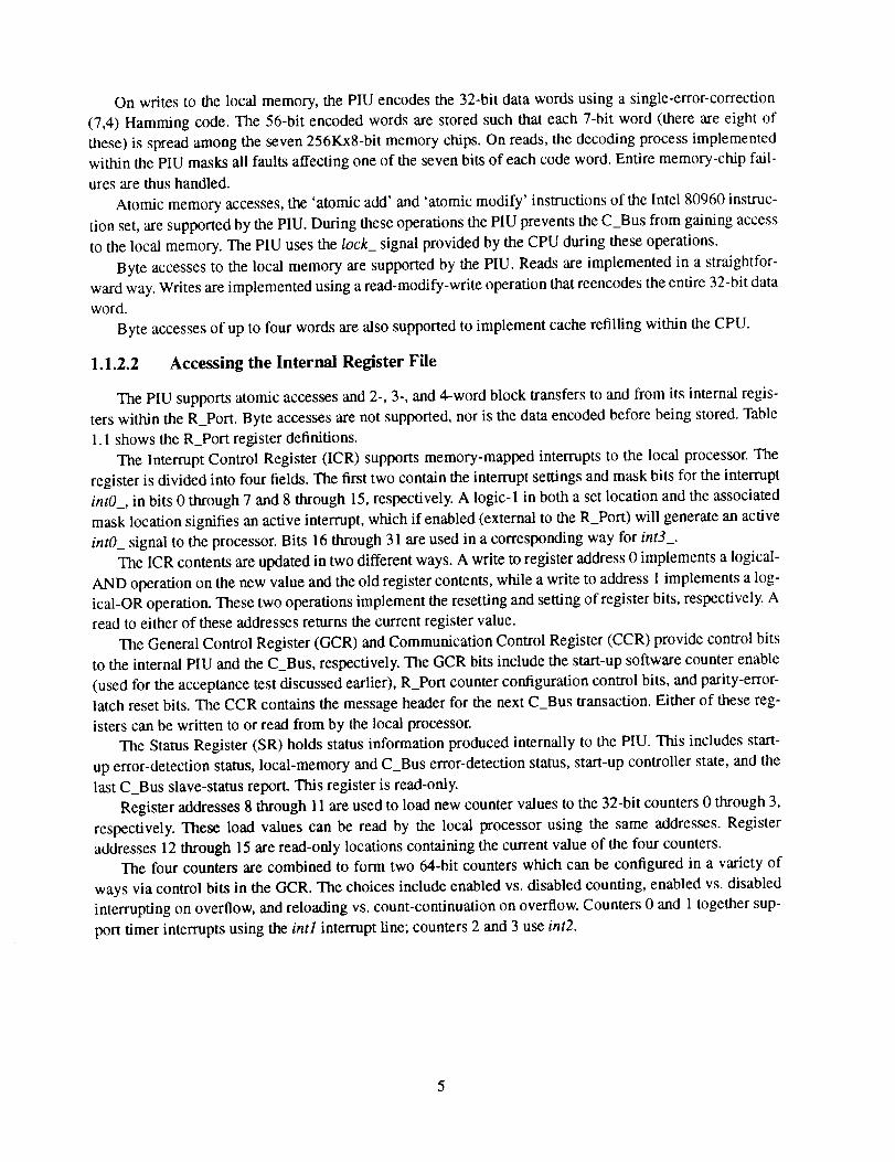
1.1.2.2 Accessing the Internal Register File
The PIU supports atomic accesses and 2-, 3-, and 4-word block transfers to and from its internal regis-
ters within the R_Port. Byte accesses are not supported, nor is the data encoded before being stored. Table
1.1 shows the R_Port register definitions.
The Interrupt Control Register (ICR) supports memory-mapped interrupts to the local processor. The
register is divided into four fields. The first two contain the interrupt settings and mask bits for the interrupt
intO_, in bits 0 through 7 and 8 through 15, respectively. A logic-1 in both a set location and the associated
mask location signifies an active interrupt, which if enabled (external to the R_Port) will generate an active
intO_ signal to the processor. Bits 16 through 31 are used in a corresponding way for int3_.
The ICR contents are updated in two different ways. A write to register address 0 implements a logical-
AND operation on the new value and the old register contents, while a write to address 1 implements a log-
ical-OR operation. These two operations implement the resetting and setting of register bits, respectively. A
read to either of these addresses reUarns the current register value.
The General Control Register (GCR) and Communication Control Register (CCR) provide control bits
to the internal PIU and the C_Bus, respectively. The GCR bits include the start-up software counter enable
(used for the acceptance test discussed earlier), R_Port counter configuration control bits, and parity-error-
latch reset bits. The CCR contains the message header for the next C_Bus transaction. Either of these reg-
isters can be written to or read from by the local processor.
The Status Register (SR) holds status information produced internally to the PIU. This includes start-
up error-detection status, local-memory and C_Bus error-detection status, start-up controller state, and the
last C_Bus slave-status report. This register is read-only.
Register addresses 8 through 11 are used to load new counter values to the 32-bit counters 0 through 3,
respectively. These load values can be read by the local processor using the same addresses. Register
addresses 12 through 15 are read-only locations containing the current value of the four counters.The four counters are combined to form two 64-bit counters which can be configured in a variety of
ways via control bits in the GCR. The choices include enabled vs. disabled counting, enabled vs. disabled
interrupting on overflow, and reloading vs. count-continuation on overflow. Counters 0 and 1 together sup-
port timer interrupts using the intl interrupt line; counters 2 and 3 use int2.
1.1.2.3
Table I.I: R_Port Register Definitions.
Register Address Contents
0 Interrupt Control Register (ICR) reset
1 ICR set
General Control Register (GCR)
Communication Control Register (CCR)
Status Register (SR)
8 Counter 0 in
9 Counter 1 in
10 Counter 2 in
11 Counter 3 in
12 Counter 0 out
13 Counter I out
14 Counter 2 out
15 Counter 3 out
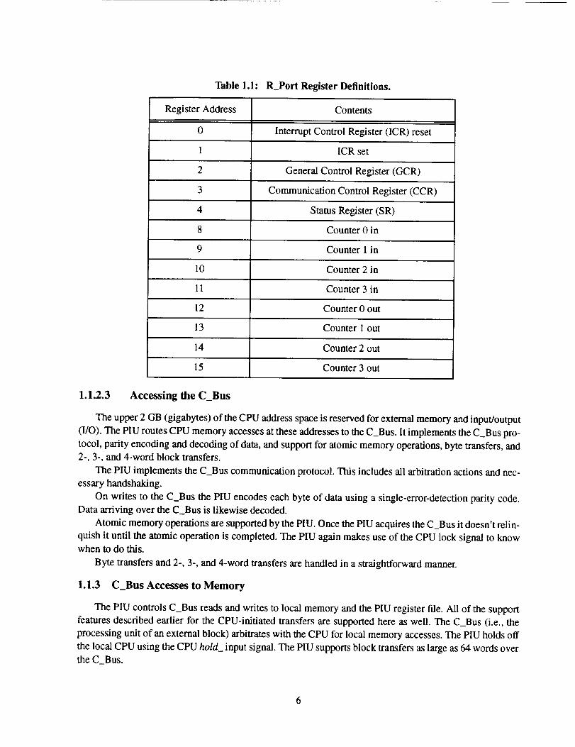
Accessing the C_Bus
The upper 2 GB (gigabytes) of the CPU address space is reserved for external memory and input/output
(I/O). The PIU routes CPU memory accesses at these addresses to the C_Bus. It implements the C_Bus pro-
tocol, parity encoding and decoding of data, and support for atomic memory operations, byte transfers, and2-, 3-, and 4-word block transfers.
The PIU implements the C_Bus communication protocol. This includes all arbitration actions and nec-
essary handshaking.
On writes to the C_Bus the PIU encodes each byte of data using a single-error-detection parity code.Data arriving over the C_Bus is likewise decoded.
Atomic memory operations are supported by the PIU. Once the PIU acquires the C_Bus it doesn't relin-
quish it until the atomic operation is completed. The PIU again makes use of the CPU lock signal to knowwhen to do this.
Byte transfers and 2-, 3-, and 4-word transfers are handled in a straightforward manner.
1.1.3 C_Bus Accesses to Memory
The PIU controls C_Bus reads and writes to local memory and the PIU register file. All of the support
features described earlier for the CPU-initiated transfers are supported here as well. The C_Bus (i.e., the
processing unit of an external block) arbitrates with the CPU for local memory accesses. The PIU holds off
the local CPU using the CPU hold_ input signal. The PIU supports block transfers as large as 64 words overthe CBus.
6
1.1.4 Timers and Interrupts
As explained above, the PIU contains two 64-bit counters and an interrupt control register. The counters
can be used to implement timed interrupts as well as a real-time clock. The timed interrupts can be pro-
grammed to provide either a single-shot interrupt or repeated, periodic interrupts.
The interrupt register is a memory-mapped register used to implement 16 possible interrupts. These
interrupts can be initiated by either the active local processor or an external C_Bus master.
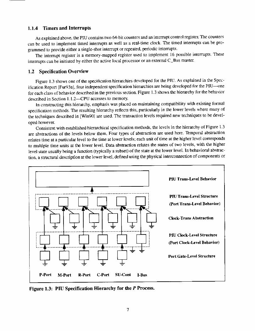
1.2 Specification Overview
Figure 1.3 shows one of the specification hierarchies developed for the PIU. As explained in the Spec-
ification Report [Fur93a], four independent specification hierarchies are being developed for the PIU--one
for each class of behavior described in the previous section. Figure 1.3 shows the hierarchy for the behavior
described in Section 1.1.2--CPU accesses to memory.
In constructing this hierarchy, emphasis was placed on maintaining compatibility with existing formal
specification methods. The resulting hierarchy reflects this, particularly in the lower levels where many of
the techniques described in [Win90] are used. The transaction levels required new techniques to be devel-
oped however.Consistent with established hierarchical specification methods, the levels in the hierarchy of Figure 1.3
are abstractions of the levels below them. Four types of abstraction are used here. Temporal abstraction
relates time at a particular level to the time at lower levels; each unit of time at the higher level corresponds
to multiple time units at the lower level. Data abstraction relates the states of two levels, with the higher
level state usually being a function (typically a subset) of the state at the lower level. In behavioral abstrac-
tion, a structural description at the lower level, defined using the physical interconnection of components or
I
P-Port M-Port R-Port C.Port SU-Cont I-Bus
PIU Trans-Level Behavior
PIU Trans-Level Structure
(Port Trans-Level Behavior)
Clock-Trans Abstraction
PIU Clock-Level Structure
(Port Clock-Level Behavior)
Port Gate-Level Structure
Figure 1.3: PIU Specification Hierarchy for the P Process.

subsystems, is replaced by a purely behavioral description at the higher level. Structural abstraction com-
bines subsystems defined at one level to form a higher level comprising their composition.
Port Gate-level structure. At the bottom of the PIU specification hierarchy is the gate-level descrip-
tion. This is a structural description derived from the lowest-level detailed design developed by the PIU
design team. The chip layout is obtained directly from this level using silicon compilation techniques that
are not within the scope of this verification task. As the bottom-most level in our hierarchy, the gate-level
models are assumed to correctly model the behavior of the physical devices, as indicated by their 'ground'
designations in the figure. Components at the gate level include individual logic gates, latches, counters, and
finite-state machines. This level is comparable to the electronic block model (EBM) level of [Win90].
Port Clock-Level Behavior. The clock-level behavioral description for each individual port, and the
I_Bus, is an interpreter model with a transition time interval of one clock period. (An interpreter is a finite-
state machine with behavior partitioned into a set of instructions). Only a single instruction is defined for
each port of the PIU however, specifying the state change and outputs of the port occurring during its exe-
cution. This level is comparable to the microinstruction level of [Win90] and elsewhere except that only a
subset of the chip design (i.e., a port) is described here rather than the entire chip.
For each of the five ports, the clock-level behavior is implemented by the corresponding gate-level
behavior shown below it in the figure--the I_Bus behavior is assumed. Other than behavioral abstraction,
there is no other abstraction between this level and the underlying gate level.
PIU Clock-Level Structure. The enclosing box around the port clock-level models represents the
clock-level structure for the entire PIU. As a structure, this representation specifies a set of constituent com-
ponents and their interconnections---the components are the actual clock-level models just described. The
interconnections are defined using the established method of forming a logical conjunction of the individual
port descriptions, using existential quantification for the signals internal to the composition (e.g., IGor86]).
Other than structural abstraction, there is no other abstraction between this description and its underlyingmodels.
Port Transaction-Level Behavior. The transaction-level behavioral description for the ports uses a
time interval corresponding to a local processor-generated transaction. A transaction here corresponds to the
transactions of the Intel 80960 microprocessor L_Bus protocol lint89]. A single transaction can represent
many clock cycles of behavior, with its time duration being nondeterministic, although bounded.
The jump in abstraction between the transaction level and the implementing clock level is very large
and is defined within a number of abstraction predicates shown in the figure. These predicates define the
temporal and data abstraction linking the state, inputs, and outputs of the corresponding models in each
level. Abstraction is by nature an asserted (rather than proved) entity and this fact is indicated by the
'ground' designation assigned to each of the abstraction models in the figure.
PIU Transaction-Level Structure. The PIU transaction-level structure is represented by the bounding
box around the port behaviors just described. This level is a structural composition of the five individual
transaction-level port specifications. The port composition is again based on the established method of form-
ing a logical conjunction, of the individual port descriptions.
PIU Transaction-Level Behavior. The PIU transaction-style behavioral description is the top-most
level in the PIU hierarchy providing a concise and easy-to-understand definition of PIU behavior. The trans-
action level specifies the PIU requirements for memory-access transactions initiated by the local processor.
Other than structural abstraction, there is no other abstraction between this description and the PIU transac-tion-level structure.

2 Processor Port Description
To prepare the reader for the discussions in Sections 3 and 4, we describe in this section the design of
the Processor Port (or P_Port) of the PIU. We focus on the P_Port because it is the target for the transaction-
level verification described in Section 4. The clock-level verification examples of Section 3 also refer to the
descriptions in this section.The circuit diagram for the P_Port is shown in Figure 2.1. As evident from the figure, the design is a
highly-distributed structure containing many primitive components. As explained in [Fur92], to simplify the
specification we have grouped certain sections of random logic into single behavioral models. This atso
speeds the verification somewhat. For example, there is an HOL definition, Req_lnputs, that defines the
behavior of the group of combinational logic indicated in the figure. All of these definitions are contained
in [Fur93b].
The figure contains several blocks that are likely to be unrecognizable to most readers. Aside from the
normal logic primitives (NAND gates, etc.), Figure 2.1 contains latches, a counter, and a finite-state
machine (FSM). Most of the non-logic elements are D-type latches. They are clocked on either phase A (A)
or phase B (R) of the clock cycle, and some contain an additional enable input (E), set input (S), and/or reset
input (Fi).The Ctr_Logic group contains a 2-bit counter that loads in a new value when the input I.O is high and
counts down, under the control of the ON input, otherwise. The FSM_Gate block is a 3-state FSM that con-
trois the P_Port operation.The shaded blocks indicate state-holding devices (again, usually latches). The names adjacent to these
blocks, beginning with P_, are the state variables of the P_Port. The P_Port inputs and outputs are, for the
most part, shown at either the extreme left or extreme right in the figure. Those variables beginning with an
L_ are Intel 80960 LBus variables, while those with an I_ are PIU I_Bus variables. The variables Fist, A,
and B, contained throughout the figure, are the reset, clock phase A, and clock phase B, respectively. The
other variables represent P_Port internal nodes.
2.1 P_Port Operation Overview
The P_Port processes memory-access transactions sourced by the active local processor of the PMM
(Figure 1. I). Transaction requests are received over the L_Bus and relayed onto the I_Bus. The informationcontained in a transaction includes the memory address, a read/write control bit, a block of (up to four) data
words, a corresponding block of byte enables, and a lock bit. These are explained below.
L_Bus transaction requests are defined by the arrival of a low I._ads_ and a high L_dan_. As seen in the
Req_Inputs group, this corresponds to a high ale signal value, which should set the P_rqt latch. The P_Port,
in turn, transmits an I_Bus request using the output signals I_male_, I_tale_, I_cale_, and I_hlda_.
An I_Bus request is defined as the combination of a high I_hlda_ and one of I_male_, I_tale_, or I_¢ale_
being low. The high I_hlda_ indicates that the P_Port, rather than the C_Port, is the current master of the
I_Bus. The other three signals distinguish the memory-request target: local memory, PIU register file, or
Core Bus, respectively.
Upon the arrival of an L_Bus transaction request, the P_Port also receives the memory address, the first
set of byte enables, and the read/write bit. The P_Port latches these values, under the control of the P_rqt
latch. For example, bit 31 and bits 2S down to 0 of the address (L_Bus signal L_ad_in) are loaded into a latch
within the Data_Latches group. The latch enable is the inverted P_rqt value. In its intended operation, the
P_rqt latch should be low upon the arrival of the request, enabling the address to be latched. On the cycles
following the request however, the P_rqt latch should be high to prevent further address loading. The byte

L_ad_out[31:0]
I
Lad In[31:0]
[31:0]
L_be_[3:0]
L_wr
AP_addr[1:0] [2S:24]
P_addr[2S:2] [23:0]
P_de=tl
[26]
lI
MERGE
_> [25:24] .'"................
a_state
n_GA TE
ScacJ.og/c
i d_stata hide_
a_stato
rile_
<_ I_ad_ln[31:0]
lad_en_
• _ I_ad_out[31:0]
hlda_
l_ I_be_[3:0]
lad_en_
I_rale_
hlda_
I_male_
I crqt_
Rst hide_
! (_ I_last_
__-'_" ..:i l_.rdy_hlds
I tardy_
I_hlda_
a_state
d_state
hide_
B
rale_
Figure 2.1: Circuit Diagram for the PIU Processor Port (P_Port).
BA
I_cgnt_
I_hold_
l_cale_
l_Iock_
I0

enables (on L_be_[3:0]) and read/write bit (on L_wr) are handled in the same way. The lock bit (on L_lock_)
also arrives during the transaction-request cycle, but is treated differently, as explained below.
Understanding the P_Port's operation requires understanding the P Port's FSM, which is described in
Figure 2.2. As seen in part (a), the FSM state variables include what might normally be thought of as FSM
'inputs' (P_lsm_rst through P_lsm_loek_), in addition to what is normally considered the 'state' (P_lsm_-
state). To accurately model the FSM's behavior however, it is necessary to define state variables for all of
these phase-B-clocked values.
P _fsm_rst
P_fsm_mr_t_sack
P_fsm_crqt_P_Nm cgnt_
P_fsm_hold_
P_h_m_lock_
p fsm_stata
combinational
logic
J
a_state
d_stata
hlda
(a) Structure.
mrqt v (--_rqt_ A -_cgnt_)a_stats d_stats
rst -_ sack /,, (hold v (-_hold A -_lock_)) -_
\\
-_ho4d_ A lock_ A sack A -_hold_ A lock_
_(mrqt v (_crqt_ A _cgnt_))
--bids_
(b) Behavior.
Figure 2.2: P_Port FSM Description.
Part (b) of the figure shows the FSM behavior. In the diagram, the input variable names are abbreviated
versions of the corresponding latch variable names. We distinguish between these values contained within
the phase-B-clocked latches (such as P_fsm_rst - abbreviated rst) and the external signals (such as Rst). The
latched values are the external signals delayed one cycle; for example, P_fsm_rst at time t+l is equal to Rst
at time t. The equations attached to the transitions define the conditions for taking the transition. The active
output signals are denoted at the states, with the understanding that it is the next state that is being indicated
here, rather than the current state. ] For example, the output a_state is high when the next state is PA (the
address state). The outputs d_state and hlda_ are similar, except that hide_ is active low.
As seen from the state machine, a P_Port reset (Rst high) moves the FSM into state PA. While in PA,
one of two events can change the state. One such event is the P_Port's gaining mastership of the PIU's
I_Bus, which moves the FSM into the data state (PD). The input-state mrqt is high if the previous cycle saw
11

thearrivalofanL_BustransactionrequesttargetingeitherthelocalmemoryorPIUregisterfile.NotefromFigure2.1thatthiscorrespondsto amost-significantaddressbit (P_destl)of logic-zero.Theinput-statecrqt_is active-lowif theCoreBuswasinsteadtargeted,in whichcasetheP_PongainsI_BusmastershiponlyaftertheC_PortacquirestheCoreBusandhasreturnedanactive-lowI_cgnt_toindicatethis.
ThePA state is also exited when the C_Port requested the I_Bus on the previous cycle (hold_ is low)
and the P_Port did not receive a simultaneous L_Bus transaction request, nor is the P_Port in the middle of
an atomic read-modify-write operation (lock_ is high). If these conditions are met then execution moves into
the hold state (PH).
The need to arbitrate for the I_Bus makes the P_Port design an interesting verification test case. It also
explains the need for P_Port latching of the address, and other L_Bus inputs, as described earlier. These
L_Bus signals are only valid during the first cycle of the transaction.
Continuing on with the FSM description, the PH state is seen to be exited upon the arrival of an inactive-
high I_hold_ signal during the previous cycle (input-state hold_ is high). An obvious requirement on the
C_Port then is that it eventually release the I_Bus in this way; otherwise the P_Port would remain trapped
in the PH state. Note that while in the PH state the I_Bus control signals sourced by the P_Port (l_male_, etc.)
are tri-stated. They are driven during this time by the C_Port.
The PD state is exited when the FSM input-state variable sack is high. This event occurs when the local
signal sack of Figure 2.1 (not to be confused with the internai-FSM sack) is high during the previous clock
cycle. The combination of two events must occur for this to happen. First, the I_Bus slave port must be trans-
mitring an active-low I_srdy_ signal, indicating the slave's successful handling of the current data word. For
write transactions, this means that the slave has finished storing the word, while for reads it indicates that
the slave is currently driving the data word onto the Iad in signal lines. I_srdy_ is transferred onto the
L_Bus as L_ready_.
An active-high sack also depends upon a P_size value of zero, which corresponds to an active-high Z
output from the counter within the Ctr_Logic group. Such a value indicates that the current data word being
processed is the last word of the block. The counter is initially loaded with the block size received over the
L_Bus as part of the address (i.e., L_ad_in[1:0]). After each word of the block is processed (and a low I_srdy_
is received) the counter is decremented, as indicated in Figure 2.1. The counter Z output is transmitted to the
slave port as I_last_ to inform it of the completion of the block. This is used by the slave in lieu of the block
size bits transmitted as I ad out[25:24] to eliminate the need for the slave to itself count down. As explained
in Section 4, this design approach adds to the difficulty in verifying the P_Port's block-size output.
The hardware at the lower left comer of Figure 2.1 implements P_Port 'memory locking' to support
atomic read-modify-write memory operations. There are two aspects to this, affecting the P_Port FSM and
affecting the I_lock_ signal that is sent to the C_Pon.
The P_Port FSM receives its lock input from the P_lock_ latch, which is intended to contain the up-to-
date version of the L_lock_ input sourced by the lntel 80960. During the 'read' portion of an atomic opera-
tion, L_lock_ is made active low by the 80960 and left low until after the corresponding write access is
started. As seen in Figure 2.2, while P_fsm_loek_ is low the FSM will not transition into the PH state, mean-
ing that it will not relinquish the I_Bus to the C_Pot't. In this way, the P_Port can successfully implement
atomic operations to the local memory and PIU register file.
The remaining 'memory lock' hardware implements the generation of the I_lock_ output. Although this
appears somewhat complicated, this logic merely ensures that I_lock_ is brought low only on atomic oper-
1. It is a coincidence that the FSM outputs and next state are correlated in this way. This FSM can be viewedas a normal Moore-type machine, meaning that the output is a function of the current state, except that weconsider all of the phase-B-clocked variables to be part of the state, rather than just P_fsm_state. We call theother phase-B variables 'input-states' in recognition that their inputs are from outside the FSM.
12

ationstotheC_Bus,andnottothelocalmemoryandthePIUregisterfile.TheC_PortusesthissignalmuchastheP_Portusesk_loek_; when it receives an active-low value it maintains ownership of the C_Bus until
it is released by an inactive-high value.
2.2 HOL Variables
The P_Port state, input, and output data structures are defined in HOL using the function define_type
from the standard type definition package. Individual elements of these structures are accessed using func-
tions defined with the new_reeursive_definition function. These definitions are contained in [Fur93b]. In this
section, we list the individual state, environment (input), and output variables to support the discussions in
Sections 3 and 4.
We use the variables s', e', and p' to represent the clock-level state, environment, and output, respec-
tively. Each of these variables is a 'signal,' meaning that it is a function, mapping time (with type :time') to
its appropriate data structure. The type :time' is an abbreviation for the HOL type tor natural numbers
(:num). For example, the state signal s' has the type :time'--->pc_state, and the application of this signal to a
particular point in time (e.g., (s' t')) yields the data structure for the state (with type :pc_state). Table 2.1 con-tains the individual state variables of the P_Port defined using accesser functions operating on the state data
structure (s' t'). For example, P_eddrS (s' t') represents the value of the P_addr latch of Figure 2.1 at time t'.
The type :worth is an HOL type representing n-bit (boolean) words. The type :wire is a 4-valued-logic type
with the values HI, LO, X, and Z, representing high, low, unknown, and high impedance, respectively; :busn
represents n-bit words of type :wire. The type :pfsm_ty contains the values PA, PD, and PH, representing theFSM state. Table 2.1 also contains the environment and output variables defined in a corresponding way. As
explained in [Fur93a], the environment and output variables are HOL 2-tuples representing the two values
contained within an individual clock cycle (one for phase A and one for phase B).
Table 2.1: P_Port HOL Variables and Their Types.
State
Variable
P_addrS (s' t')
Type
P_fsm_crqt_S (=' t')
:worcln
P_dutlS (s' t') :bool
P_be_S (=' t') :wordn
P_wrS (=' t') :bool
P_Mm_stateS (s' t') :pfsm_ty
P_fsm_rstS (s' t') :bool
P_fsm_mrqtS (s' t') :bool
P_fsm_sackS (s' t') :bool
:bool
P_fsm_cgnt_S (l' t') :bool
P_fsm_hold_S (s' t') :heel
P_fsm_lock_S (s' t') :heel
P_rqtS (s' t') :heel
Environment
Variable
RitE (e' t')
L_ad_lnE (e' t')
Type
:bool#bool
:wordn#wordn
OutputVariable
L_ad_outO (p' t')
L_remdy_O (p' t')
Type
:busn#busn
:bool#bool
L_ads_E (e' t') :bool#bool I ad outO (p' t') :busn#busn
L_den_E (e' t') :bool#bool l_be_O (p' t') :buen#busn
L_be_E (e' t') :wordn#wordn l_rale_O (p' t') :wlre#wlre
L_wrE (e' t')
L_lock_E (e' t')
l_ad_inE (e' t')
l_cgnt_E (e' t')
I_hold_E (e' t')
l_srdy E (e' t')
: bool#bool I_mele_O (p' t') :wire#wire
:bool#bool I_crqt_O (p' t') :bool#bool
:wordn#wordn I_cale_O (p' t') :bool#bool
:bool#bool I_mrdy_O (p' t') :wire#wire
I_last_O (p' t')
I_hlda_O (p' t')
:bool#bool
:bool#bool
I_tock_O (p' t')
:wire#wire
:bool#bool
:bool#bool ]1
13

Table 2.1: P_Port HOL Variables and Their Types.
State
Variable
P_slzeS (s' t')
Type
:wordn
P_loadS (s' t') :bool
P_downS (s' t') :bool
P_lock_S (s' t') :bool
P_lock_inh_S (s' t') :bool
P_maleS (s' t') :bool
P_rale_S (s' t') :bool
Environment
Variable Type
//OutputVariable
llType
14

3 PIU DesignVerification
This section describes the verification of the clock-level behavioral models for each of the five PIU
ports, with respect to their implementing gate-level models. Section 3.1 overviews the clock-level verifica-
tion problem and the approach used to solve it. Section 3.2 describes the tactic used to handle the standard
cases. Both of these subsections make use of the P_Port for clarifying examples. Section 3.3 explains the
more-difficult cases arising within the P_Port and the R_Port, and it outlines their solution. Section 3.4 pro-
vides a concluding discussion.
3.1 Overall Approach
The implementation correcmess theorem statement for each port follows the form of the P_Port theorem
shown here:
P_Clock_Correct:I- V s' e' p'. PBIock_GATE s' e' p' _ PCSet_Correct s' e' p'
The predicates PBIock_GATE and PCSet_Correct are the models for the gate-level structure and clock-level
behavior, respectively. The variables s', e', and p' are the state, environment, and output signals described
in Section 2.
PCSet_Correet characterizes the behavior of the entire P_Port instruction set, in terms of the individual-
instruction predicate PC_Correct:
I -a_f V s' e' p'. PCSet_Correct s' e' p' = V pci t'. PC_Correct pci $' e' p' t'
The variable pci represents the instruction under consideration. At this level there is only one: PC_X. The
variable t' represents clock-level time, where each increment corresponds to a single cycle of the PIU input
clock (piu_clk of Figure 1.1). The variables s', e', and p' are the same as before.From its definition PCSet_Correct is seen to be true only if PC_Correct is true for all instructions pci and
all time t'. PC_Correct is itself defined in terms of the instruction execution predicate PC Exec, the instruc-
tion precondition PC_PreC, and the postcondition PC_PostC:
I-,uf V pci s' e' p' t'. PC_Correct pci s' e' p' t' PC_Exec pci s' e' p' t' ^PC_PreC pci s' e' p' t'
PC_PostC pci $' e' p' t'
This predicate is read as "for all instructions pci and all time t' (and all s', e', p'), if pci is executed at t' and
if the precondition is true for pci at t', then the postcondition is true for pci at t'. This defines instruction cor-
rectness for individual instructions at single points in time.
15

Theexecution,precondition,andpostconditionpredicatesaredefinedasfollows:
I-def V pci s' e' p' t'. PC_Exec pci s' e' p' t'
I-def V pci s' e' p' t'. PC_PreC pci s' e' p' t'
I-def V pci s' e' p' t'. PC_PostC pci s' e' p' t'
= T
= T
= (s' (t'+l)) = PC_NSF(s't') (e't')) /x(p' t' = PC_OF (s' t') (e' t'))
PC_Exec is universally true since there is only one instruction for this level and it is executed every
cycle; Pe_PreCis also true, indicating that no special preconditions are necessary here. The pre-post inter-preter model is an overkill in this situation--a simple finite-state machine model would suffice.
The postcondition PC_Posit provides the definition for correct clock-level behavior in terms of the
next-state function PC_NSF and the output function PC_OE These functions take as inputs the current state
(s' t') and current inputs (e' t'), and return the next-state and output, respectively. Each is much too long to
include here however. The interested reader is referred to the [Fur93b] for details of these functions.
As seen in the next section, proving the correctness theorem P_Cloek__Correet is conceptually verystraightforward.
3.2 Standard Cases
To clarify what needs to be proved, the theorem statement P_Clock_Correct from above is shown herewith several of its definitions rewritten.
Rewritten Theorem Statement:
V pci s' e' p' t'. PBIock_GATE s' e' p' (s' (t'+l)) = PC_NSF (s' t') (e' t')) /x
(p' t' = PC_OF (s' t') (e' t'))
An advantage of the we-post interpreter model's specification style is the use of an explicit instruction
variable (pei here), which helps to guide the verification process. In previous interpreter verification
approaches, performing a case split on the instruction set was not so easy. In fact, one of the contributions
of the generic interpreter theory [Win90] was its 'behind-the-scenes' handling of several proof steps to pro-vide the user with a refined set of proof obligations, corresponding to the individual instructions to be veri-fied.
The "for all pei" in the above theorem statement makes clear the need to perform a case split on theinstruction set. This is easily accomplished in HOL using the tactic INDUCT_THEN. 1
1. The lack of any dependence upon pci within the body of the above goal makes the above discussion some-
what irrelevant to the immediate example. For instance, pci could also be eliminated here using the tacticGEN_TAC, etc. The discussion is directed more towards the general interpreter verification problem.
16

The tactic STRIP_TAC can be used here to specialize the state, environment, output, and time variables
and move the implementation PBIoek_GATE s' e' p' into the assumption list. Then CONJ_TAC can be used to
split the goal into the following two subgoals:
Subgoal 1:
Subgoal 2:
s' (t'+l) = PC_NSF (s' t') (e' t')
[ PBIock_GATE s' e' p' ]
p' t' = PC_OF (s' t') (e' t')
[ PBIock_GATE s' e' p' ]
At this point we have the option of rewriting the subgoals and assumptions using the next-state defini-
tion (subgoal 1) and the implementation, and proceeding from there. This is a bad choice however. The
amount of detail contained within PC_NSF (and PC_OF) is overwhelming, and makes such a direct approach
impractical. Instead, it is far better to initially prove a theorem for each of the individual elements of the
state and output data structures. These theorems can then be used to derive the above two subgoals.
Consider the subgoal for the next state (subgoal 1). As described in Section 2, the next-state data struc-
ture (s' (t'.l)) contains 20 elements: P_addrS (s' (t'+l)) through P_rale_S ($' (t'+l)). For each of these, we
prove a theorem comparable to P_addrS_THM below. Having this, we use the tactic IMP_RES_TAC (20 times)
to move the consequences of each of these theorems into the assumption list, where they are then available
for rewriting with. Only a few minor proof steps are required to finish the proof. The details of this and the
prior steps are contained in [Fur93c].
P_addrS_THM:
I- V t' s' e' p'. PBIock_GATE s' e' p' _ (P_addrS (s' (t'+l)) = P_addrS (PC_NSF (s' t') (e' t')))
The following 3-line tactic, suitably customized, proves the vast majority of the theorems P_addrS_THM
through P_raleS_THM.
REWRITE_TAC [P_addrS; PBIock_EXP; PC_NSF_EXP]THEN REPEAT STRIP_TACTHEN ASM_REWRITE_TAC [ ]
The first step rewrites the goal (the theorem statement) using the definitions of the variable accessor
function P__addrS, an 'expanded' version of the gate-level implementation (PBIoek_EXP) and an 'expanded'
version of the next-state function (PC_NSF_EXP). The expanded version of PBIoek_EXP, for example, has
all of the components in the gate-level structure already rewritten according to their definitions.
The second step in the proof moves the rewritten implementation (PBIock_GATE) into the assumption
list where it can be used in the third step to rewrite the left-hand side of the remaining goal (P_addrS (s' (t'
+ 1))). From this description it is evident that the left-hand side of the above equality represents the next-
state behavior of P_addr implemented by PBIoek_GATE, while the fight-hand side is that specified by the
clock-level next-state function PC_NSF.
This 3-line tactic is the standard proof technique for structural-to-behavioral proofs where no temporal
or data abstraction exists between the two levels. Discovering the importance of avoiding abstraction here
was an important contribution of earlier work under this contract (e.g., [Win90]). Except for cases such as
17
thosedescribedin thenextsection,onceallspecificationerrorswereeliminated,theclock-levelcorrectnessproofsweretrivialtocomplete.
3.3 The Harder Cases
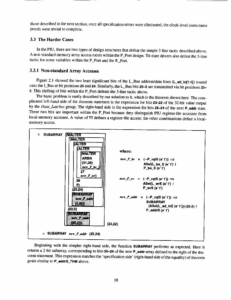
In the PIU, there are two types of design structures that defeat the simple 3-line tactic described above.
A non-standard memory array access exists within the P_Port design. Tri-state drivers also defeat the 3-line
tactic for some variables within the P_Port and the R_Port.
3.3.1 Non-standard Array Accesses
Figure 2.1 showed the two least significant bits of the L_Bus address/data lines (L_ad_in[1:0]) routed
onto the I_Bus at bit positions 2s and 24. Similarly, the L_Bus bits 25-2 are transmitted via bit positions 23-0. This shifting of bits within the P_Port defeats the 3-line tactic above.
The basic problem is easily described by our solution to it, which is the theorem shown here. The com-
plicated left-hand side of the theorem statement is the expression for bits 23-22 of the 32-bit value output
by the Data_Latches group. The right-hand side is the expression for bits 25-24 of the next P_addr state.
These two bits are important within the P_Port because they distinguish PIU register-file accesses from
local-memory accesses. A value of'IT defines a register-file access; the other combinations define a local-
memory access.
I- SUBARRAY (MALTER Ii'(MALTER II
(25,24)
(2a,o)
= SUBARRAY new P add" (25,24)
(23,22)
where:
new_P_be = (-_P_rqtS (s' t')) ==:>
ASel(L_be_E (e' t') I
P_be_S ($' t')
new_P_wr = (-_P_rqtS (s' t')) =::>ASeI(L_wrE (e' t') IP_wrS (s' t')
new P addr = (-_P_rqtS (s' t')) =::>
SUBARRAY
(ASel(L_ad_inE (e' t'))) (25,0) I
P_addrS ($' t')
Beginning with the simpler right-hand side, the function SUBARRAY performs as expected. Here it
returns a 2-bit subarray, corresponding to bits 25-24 of the new P_,,ddr array defined to the right of the the-
orem statement. This expression matches the 'specification side' (right-hand side of the equality) of theoremgoals similar to P_addrS_THM above.
18

Theleft-handsideof the above theorem statement matches the 'implementation side' of theorem goals
such as P_addrS_THM, which are rewritten with the components of PBIock_GATE. The portion of the above
expression within the outermost box is a 32-bit array whose bits 31-28 are the next-state value of P_be_, bit27 is the next-state value of P_wr, and so on. The function ALTERf i x returns an array whose i'th element is
x, and whose other elements are those off. MALTERhandles multi-bit updates in a similar fashion. ARBN is
an array, all of whose elements are arbitrary values. All of these are described in more detail within the Spec-
ification Report [Fur93a].The theorem above was straightforward to prove. Named lemmal within Section 3. l of [Fur93c], it was
used in the third line of the standard 3-line tactic to rewrite the implementation side of the theorem goal, and
successfully completed several of the PPort proofs.
3.3.2 Tri-State Buses
Tri-state buses lead to more difficult theorem-proving problems than above, primarily because they
require quantitative reasoning with n-bit words, which is currently not well supported by our wordn_defthe-
try. For example, using the HOL reduce library, one can directly prove the inequality: _ (5 = 7). However,
proving the comparable fact for n-bit words, (9 0NORDN 3 5 = WORDN 3 7)) is not automatic and is quite
tedious.
Proofs such as this are necessary in the R_Port verification to show that multiple outputs of a register-
file address decoder are not true at the same time. If more than one were true, then multiple R_Port bus driv-
ers would be simultaneously driving onto a common bus, which would be a serious design flaw. In lieu of
a complete arithmetic library for n-bit words comparable to reduce, which is planned future work, we have
proven the following special-purpose theorem for the 4-bit case within the R_Port:
I- Vnm. n_<15 :_ m_<15 :D -_(m=n) :D _(WORDN3m=WORDN3 n)
This theorem statement is very straightforward, and it clearly defines the preconditions necessary to
establish the appropriate n-bit-word inequalities. To use tiffs theorem in practice, we first obtained a theorem
for each precondition (5 _<15, for example) using REDUCE_CONV, which we added to the assumption list
using ASSOME_TAC. We then used IMP_RES_TAC, with the above theorem, to establish the desired inequal-
ity in the assumption list, for subsequent use in rewriting the goal.
Although this procedure is conceptually straightforward, in practice it requires more theorem-proving
effort than it should. We expect to put more work into strengthening our wordn_deftheory to make future
proofs like this easier. Section 3.3 of [Fur93c] contains the details of the R_Port clock-level proof.
3.4 Discussion
The PIU clock-level verification took approximately four man-months, which included time spent con-
vetting our component library from the phase level to the clock level, as described in the Specification
Report [Fur93a]. Altogether there are theorems for approximately 170 next-state variables and 60 outputvariables. Some enhancements to our wordn_def theory were required, as was the development of a new
theory for implementing 4-valued logic: busn_def.Most of our time was spent finding and correcting bugs in the clock-level specifications. Although we
used great care in constructing these models, there remained many mistakes. Furthermore, the large amount
of detail in the port specifications required tedious and time-consuming searches for these mistakes. In this
section, we present some ideas for making future tasks of this type more efficient.
19

Our experience on this task suggests that a behavioral version of the lowest-level structural description,
like the clock level, is an important level within a specification hierarchy. While most of the proofs for the
individual next-state and output variables were easy to construct, the CPU-time requirements for these
proofs were significant in many cases. This is because of the large amount of rewriting that is necessary in
circuits containing many components. Having an already-verified behavioral level, before attempting proofs
at higher specification levels, greatly improves theorem-proving efficiency there.
The remainder of this section discusses three areas where future work should be targeted to make clock-
level verification a practical activity. The first is the automated generation of gate-level models. This is fol-
lowed by the automated generation and verification of clock-level models. Finally, we discuss an approachfor incorporating buses into the above approach.
3.4.1 Generation of Gate-Level Models
A high priority for any future work is the automated generation of HOL gate-level specifications from
the implementation descriptions (simulation models or netlists). It should be relatively straightforward to
construct a translation program to do this based purely on the structural information contained within the
description. Even a translation not based on a formal semantics is extremely important in helping make the-
orem-proving-based verification a practical activity, as well as helping to ensure the accuracy of the lowest-level specification model.
3.4.2 Generation and Verification of Clock.Level Models
The automated generation of clock-level models from the gate-level specification should also be pur-
sued. There is a systematic way to do this, using the lot construct of the HOL logic to define the intermediate
signal values present on the circuit's internal nodes. In fact, this is similar to the manual procedure that we
used to create the clock-level models for the PIU. Figure 3.1 demonstrates the idea. It shows an example
circuit structure in part (a) along with its behavioral representation in part (b). The behavior is represented
as a function, in a manner compatible with both the pre-post interpreter model and the generic interpretermodel of [Win90].
In2
In3 out
In4
(a) Example Circuit.
I-kf out_function In1 In2 in3 |n4 =
leta = -_(Inl ^ In2) in
let b = -_(In3 ^ in4) Inletc= -_(a ^ b) Inlet out = -_c Inout
(b) Corresponding HOL Function.
Figure 3.1: Correspondence Between an Example Structure and its Behavioral Definition.
As in this figure, the procedure for constructing clock-level models works with nodes at the outputs of
logic gates whose inputs are already defined, either because they are system inputs, current state values, or
previously defined within a let construct. In practice, this is done twice - once to construct the next-state
function and once for the output function.
There is no reason to stop here. A further advancement would be the automated verification of the clock
level with respect to the gate level, using routines coded in the HOL interface language ML (see IGor88]).
As explained above, most of the next-state and output variables can be proven using a similar 3-line tactic.
Those that cannot be proved this way can, in the worst case, be performed by hand. A better approach though
20

wouldbetointerveneearlierwithinthedesignprocessitself.Forexample,insteadof permittingdesignerstousetri-statebuffersin anarbitraryway,it mightbebetterto provide'busmodules,'asdescribedin thenextsection.
3.4.3 Bus Modules
Bus modules support clock-level proof automation by 'preprocessing' the difficult proof steps involving
tri-state drivers. The basic idea is described in Figure 3.2, where a four-input bus is described graphically
(part (a)) and behaviorally (part (b)). The components in the module are the tri-state drivers and a decoder,
which outputs a single high value that is determined by its 2-bit input combination.
$ell
sol2
In1
In2
In3
In4
(a) Example Bus Module.
I-.f bus_module sol1 eel2 din1 din2 din3 din4 out
VL
out t =
(-_ sell t ^ -_ eel2 t) _ in1 t I
out (--_sell t ^ eel2 t) _ in2 t I
(eel1 t A -_sel2 t) _ in3 t
% (sell t A eel2 t) % I in4 t
(b) Corresponding HOL Definition.
Figure 3.2: Example Bus Module and its Gate-Level Definition.
The important aspect to this idea is that HOL gate-level models would be constructed using bus module
specifications, such as the HOL definition of bus_module in the figure, rather than the models for the indi-
vidual components. These module specifications would be pre-verified, and so could safely be used in the
automated approach discussed in the last section.A choice would need to be made concerning the generation of the HOL specifications for these modules
however. The approach having the least impact on current design practice is to rely on the gate-level trans-
lator to find instances of these modules, perhaps distributed within the design, to construct the HOL models.
A designer would be constrained mainly in the required use of a decoder to produce the tri-state enables,
which is a good design practice anyway.
Another approach is to introduce bus modules into the designers' component library and mandate that
they be used instead of the individual components of the modules. This is not likely to be resisted by design-
ers, but it does have a potential impact on the layout of the individual bus components. For example, it may
be desirable to distribute the drivers over a wide physical area. If an automated layout tool is used, this may
require special attention in the layout algorithm. Another approach is to overlay bus modules on top of the
existing design environment, and translate them into the 'normal' components. Bus modules in this sce-
nario, aside from serving as the HOL translation source, merely provide a 'syntax check' on the design.
To conclude, bus modules can play an important role in helping make theorem-proving-based verifica-
tion of low-level hardware an efficient and secure process. There is a limitation to this approach however,
in that it works only with buses that have localized control, which essentially means that all of the bus
enables are generated (by a single decoder) within the subsystem under consideration. However, this
approach would have been applicable to the buses within the R_Port and P_Port of the PIU. But the PIU's
21
I_Bus,whichhascontroldistributedamongfourof theports,is anothermatter.TheSpecificationReport[Fur93a]explainshowdistributed bus control can be handled in a secure manner.
22

4 PIU Requirements Verification
This section describes the partial verification of the transaction-level behavior of the P_Port, for trans-
actions initiated by the local processor. Of the three next-state variables and nine output variables of the
P_Port, we have completed the proof for the address output variable (IB_Addr_out) and most of the proof
for the block-size output variable (IB_BS_out). As explained in this section, the work completed so far rep-
resents approximately 80-90% of the P-Port verification.
Section 4.1 lists and explains some of the important signals of the P_Port, and it describes the significant
events defined by these signals and the time variables that denote them. Section 4.2 explains the overall ver-
ification approach used for the transaction verification. Section 4.3 describes the address verification. Sec-
tion 4.4 describes the partially-completed block-size verification. Section 4.5 finishes with a concluding
discussion.
4.1 P_Port Description
Section 4.1.1 describes significant P_Port signals and Section 4.1.2 describes the important event times.
In the descriptions that follow, transaction-level times use unprimed variables; clock-level variables are
primed.
4.1.1 Signals
A number of signals have been defined to make the transaction-level specification more compact and
readable. They also help to simplify the verification in some cases by avoiding the need to perform case
splits. In this section we describe four such signals that see considerable use later in the description of the
P_Port verification. All of these signals are functions, with types :timeC-_bool.
The signal ale_sifl_pb defines the presence (or absence) of local-processor memory requests. When true,
it indicates that the local processor is requesting an L_Bus transaction. This signal was shown in Figure 2.1
as ale, and is defined in terms of L_Bus clock-level signals as follows:
I-ae/ V e'. ale_sig_pb e' = )_ u', -_BSel(L_ads_E(e' u')) /x BSel(L_den E(e' u'))
BSel is an accessor function that returns the phase-B portion of the clock-level variable. As explained in Sec-
tion 2, L_ads_E and L_den_E are also accessor functions that, when applied to the environment structure (e'
u' above), return the values corresponding to the signals L_ads_ and L_den_, respectively.
The signal ale_sig_ib is the corresponding IBus version of ale_slg_pb, indicating that the P_Port is ini-
flaring an I_Bus transaction. It is defined as follows:
I-def V p'. ale_sig_ib p' ;_ u'. BSel(l_hlda_O(p' u')) /x ((BSel(l_male_O(p' u')) = LO) v
(BSel(l_rale_O(p' u')) = LO) x/
-_BSel(l_cale_O(p' u')))
As before, the functions I_hlda_O, etc. are accessor functions, in this case returning values from the P_Port
output data structure.This signal has no physical counterpart within the P_Port design, but it indicates the precise conditions
under which the P_Port initiates an IBus transaction. When the signal I_hlda_ is true the P_Port, rather than
the C_Port, drives the IBus mastership signals I_mrdy_, I_last_, etc. An active low Imale_, I_rale_, or
23

I_cale_ indicates an M_Port, R_Port, or C_Port memory request, respectively. Both I_male_ and I_rale_ are
outputs of tri-state buffers thus they are of 4-value-logic type ":wire".
The signal ack_sig_ib is defined as follows:
[ I-def V e' p'. ack_sig_ib e' p' = _. u'. (BSel(l_last_O(p' u')) = LO) A -_BSel(l_srdy_E(e' u'))
When this signal is true at a clock-level time u', it indicates that the active portion of the current trans-
action is over at time u'. The P_Port supplies the signal I_last_ to indicate when the last word is beingaccessed. The I_Bus slave provides the signal I_,rdy_.
The signal rdy_sig_ib is similar to ack_sig_ib in that it indicates the presence of an active I_srdy_, but
the inactive I_last_ output indicates that only an intermediate data-word access is being completed, ratherthan the entire active transaction. Its definition is as follows:
I-de/ V e' p'. rdy_sig_ib e' p' = _. u'. (BSel(l_last_O(p' u')) = HI) A -_BSel(l_srdy_E(e' u'))
4.1.2 Significant Event Times
Within a given transaction are several important times that correspond to the major events within the
transaction. These are times measured on the clock-level scale, occurring between the transaction-level
times t and t+l. Figure 4.1 shows these times plotted along with their defining events, which are themselves
defined using the signals described in the last section.
tp' U' t'rayO t'rdyl
era#t'ray2 t'sack tp'muc
I I I
I Iack_sig_ib e' p' t'sack
rdy_slg__lb e' p' t'rdy2
rdy_slg_lb e' p' t'rdyl
rdy_sig_lb e' p' t'rdyO
ale__sig_ib p' tl'
ale__sig_pb e' tp'
Figure 4.1: Significant Events and Times Within a P_Port Transaction.
The clock-level variable tp' represents the beginning of the transaction interval, defined by the arrival
of local-processor memory request (ale_sig._pb e' tp' ]s tl'ue). This is the concrete time corresponding to the
P_Port transaction-level time t. The 'p' signifies a 'processor-bus' transaction time--the Intel L_Bus is
sometimes given the generic designation 'P_Bus.'
The variable ti' represents the time that the P_Port initiates an I_Bus transaction (ele_sig_ib p' ti' is true)
in response to the processor L_Bus request. This transaction is either begun immediately, or else forced to
wait because of a busy I_Bus (as in Figure 4.1). Within a given transaction then, we have tr _>tp'.
The variables t'rayO, t'rdyl, t'rdy2, and t'rdy3 represent the times that the I_Bus slave port (the P_Port is
the I_Bus master) responds with an active-low I_srdy_ signal, indicating that the slave has finished process-
24

ingthecurrentdataword.Fordatawritesthismeansthattheslaveis ready to receive the next word, whilelot data reads this means that the slave is currently sourcing a valid data word. Not all of these times are
applicable for a given transaction however--they are used, from left to right, as the number of data words
in the transaction (i.e., the block size) is increased from one to four. Figure 4.1 shows the case for a block
size of four.
The variable t'saek is used to represent the time that I srdy_ becomes active-low to end the active part
of the current transaction. It therefore represents the same time as one of the t'rdy variables, depending on
the block size. The 'sack' within this variable name is taken from the signal with the same name shown in
Figure 2.1. It is a shorthand for 'slave acknowledge.'The clock-level variable tp'sue represents the time that a new transaction request arrives over the
L_Bus. This event officially marks the end of the current transaction and the beginning of a new one. The
interval between t'saek and tp'sue represents idle time; we sometimes refer to t'saek as the end of the 'active"
part of the transaction. Just as tp' corresponds to the transaction-level time t, tp'sue marks the clock-level
time corresponding to t+l.
4.2 Overall Verification Approach
The implementation correctness theorem statement for the P_Port transaction level is as follows:
P_Trans_Correct: I- V s e p s' e' p'. PCSet_Correct s' e' p'PTAbsSets e p s' e' p'
PTSet_Correct s e p
The predicates PCSet_Correct and PTSet_Correct are the models for the clock-level and transaction-level
P_Port behavior, respectively. The predicate PTAbsSet is the abstraction predicate that relates the variables
of the clock level and transaction level. The variables s, e, and p represent signals mapping transaction-level
time to transaction-level state, input, and output, respectively. The variables s', e', and p' are the correspond-
ing signals for the clock level, which have already been used in Sections 2 and 3.
4.2.1 Transaction-Level Interpreter
Like the definition of its clock-level counterpart, PTSet_Correct is defined in terms of an individual-
instruction correctness predicate:
I-_f V s e p. PTSet_Correct s e p = V pti t. PT_Correct pti s e p t
The instruction and time variables, pti and t, represent transaction-level entities. Unlike the clock level
where only a single instruction was defined, here there are two: PT_Write and PT_Read, for handling data
writes and reads, respectively.The individual instruction correctness predicate PT_Correet is defined similar to before:
I-def V pti S e p t. PT_Correct pti s e p t PT_Exec pti s e p t APT_PreC pti s e p t
PT_PostC pti s e p t
25
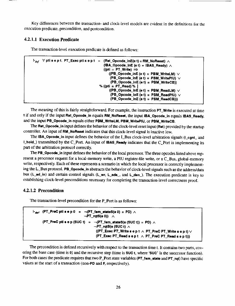
Key differences between the transaction- and clock-level models are evident in the definitions for the
execution predicate, precondition, and postcondition.
4.2.1.1 Execution Predicate
The transaction-level execution predicate is defined as follows:
l-a,/ Vptisept. PT_Execptisept = (Rst_Opcode_inE(e t) = RM_NoReset) A(IBA_Opcode_inE (e t) = IBAS_Ready) A((pti = PT_Write) =¢
((PB_Opcode_inE (e t) = PBM_WriteLM) v(PB_Opcode_inE (e t) = PBM_WritePIU) v(PB_Opcode_inE (e t) = PBM_WriteCB))
% ((pti = PT_Read) % I((PB_Opcode_inE (et) = PBM_ReadLM) v(PB_Opcode_inE (e t) = PBM_ReadPIU) v(PB_Opcode_inE (e t) = PBM_ReadCB)))
The meaning of this is fairly straightforward. For example, the instruction PT_Write is executed at time
t if and only if the input Flst_Opcode_in equals FIM NoFleset, the input IBA_Opcode_in equals IBAS_FIeady,
and the input PB_Opcode_in equals either PBM_WriteLM, PBM_WritePIU, or PBM_WriteCB.
The Rst_Opcode_in input defines the behavior of the clock-level reset input (Rst) provided by the startup
controller. An input of FIM_NoFleset indicates that this clock-level signal is inactive low.
The IBA_Opcode_in input defines the behavior of the I_Bus clock-level arbitration signals (l_egnt and
I_hold) transmitted by the C_Port. An input of IBAS Fleady indicates that the CPort is implementing its
part of the arbitration protocol correctly.
The PB_Opcodo_in input defines the behavior of the local processor. The three opcodes listed above rep-
resent a processor request for a local-memory write, a PIU register-file write, or a CBus, global-memory
write, respectively. Each of these represents a scenario in which the local processor is correctly implement-
ing the L_Bus protocol. PB_Opcode_in abstracts the behavior of clock-level signals such as the address/data
bus (L_ad_in) and certain control signals (L_wr, L_ads_, and L_den_). The execution predicate is key to
establishing clock-level preconditions necessary for completing the transaction-level correctness proof.
4.2.1.2 Precondition
The transaction-level precondition for the P_Port is as follows:
I-aef (PT_PreC pti • • p 0 = -_(PT_fsm_stateS(s O) : PD) A-_PT_rqtS(s 0)) A
(PT_PreC pti • • p (SUC t) = -_(PT_fsm_stateS(s (SUC t)) = PD) A-_PT_rqtS(s (SUC t) A
((PT_Exec PT_Write s e p t A PT_PreC PT_Write s • p t) v
(PT_Exec PT_Read s • p t A PT_PreC PT_Read s e p t)))
The precondition is defined recursively with respect to the transaction time t. It contains two parts, cov-
ering the base case (time is 0) and the recursive step (time is SUe t, where 'SUO' is the successor function).
For both cases the predicate requires that two P_Port state variables (PT_fsrn_state and PT_rqt) have specific
values at the start of a transaction (non-PD and F, respectively).
26

Theremainingpartofthepredicateassertsthataninstructionwasexecutedduringthepriortransaction-leveltimeandthatitspreconditionwassatisfied.Thereasonfor includingthispreconditiononapriorexe-cutionis thatseveralofourinductionproofshaverequiredit. Thisissomethingthatweaddedafterattempt-ingproofsofthesetype.Wedon'tbelievethatit causesanyfundamentalproblems,sinceif apriorexecutiondoesnotexistthentheenvironmentof theP_Portwaserroneousandin thisscenariowecouldnothopetoknowthePPort's conditionattransactionstart.Asmentionedin theSpecificationReport[Fur93a],futureworkwill addresseliminatingtheneedforthispartof thepredicate.
4.2.1.3 Postcondition
The transaction-level postcondition for the P-Port is as follows:
I"def Vptisept. PT_PostCptisept =(pti = PT_Write) => (((s (t + 1) = PT_WriteNSF_A (s t) (et)) v
(s (t + 1) = PT_WriteNSF_H (s t) (e t)) A(p t = PT_WriteOF (s t) (e t)))
% (pti = PT_Read) % I (((s (t + 1) = PT_ReadNSF_A (s t) (e t)) v(s (t + 1) = PT_ReadNSF_H (s t) (e t)) A(p t = PT_ReadOF (s t) (e t)))
For each of the transaction-level instructions, the next state is defined by one of two next-state functions.
One of these defines the next FSM state variable to be PA, the other defines it to be PH. This is the same
condition as seen in the precondition, that is, non-PD. Each instruction contains a single function defining
the P_Port output.
The need for two next-state functions is dictated by the presence of the C_Port, which can request the
IBus. If it does so prior to the P_Port's receiving an L_Bus request to begin a new transaction (defining the
time t+l) then the P_Port will be in the PH, or hold, state. Otherwise it will be in the PA, or address, state.
4.2.2 Abstraction Predicate
The abstraction predicate PTAbsSet defines the relationship between the P_Port signals at the transac-
tion level and those at the clock level. It is defined in terms of the individual-instruction abstraction predicate
PTAbs as follows:
I-d,,/ Vseps'e'p'. PTAbsSetseps'e'p' = Vptit. PTAbsptisepts'e'p' [
PTAbs is itself defined as:
I-def V pti s ep t s'e' p'. PTAbs pti s e p t s' e' p' =
(PT_Exec pti s e p t3 tp'. NTH_TIME_TRUE t (ale_sig__pb e') 0 tp' ^ (tp' > 0))
(V tp'. NTH_TIME_TRUE t (ale_sig_pb e') 0 tp'
D (Rst_Slave pti e t e' APB_Slave pti e p t e' p' tp' AIBA_PMaster pti e p t e' p' APStateAbs pti s e p t s' e' p' tp')) A
(V ti'. NTH_TIME_TRUE t (ale_$ig_ib p') 0 ti'IB_PMaster pti e p t e' p' tr)
A
27
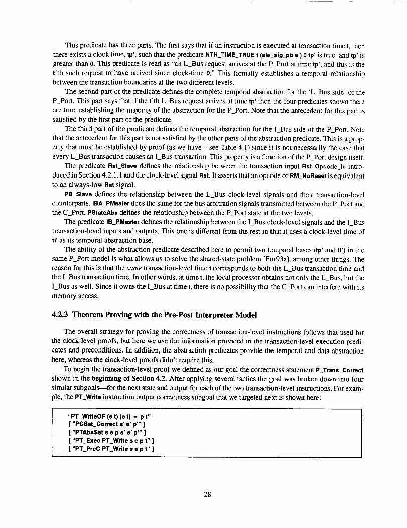
This predicate has three parts. The first says that if an instruction is executed at transaction time t, then
there exists a clock time, tp', such that the predicate NTH_TIME TRUE t (ale_sig_pb e') 0 tp' is true, and tp' is
greater than O. This predicate is read as "an LBus request arrives at the P_Pon at time tp', and this is the
t'th such request to have arrived since clock-time o." This formally establishes a temporal relationshipbetween the transaction boundaries at the two different levels.
The second part of the predicate defines the complete temporal abstraction for the 'L_Bus side' of the
P_Port. This part says that if the t'th LBus request arrives at time tp' then the four predicates shown there
are true, establishing the majority of the abstraction for the P_Port. Note that the antecedent for this part is
satisfied by the first part of the predicate.
The third part of the predicate defines the temporal abstraction for the I_Bus side of the P_Port. Note
that the antecedent for this part is not satisfied by the other parts of the abstraction predicate. This is a prop-
erty that must be established by proof (as we have - see Table 4. l) since it is not necessarily the case that
every L_Bus transaction causes an I_Bus transaction. This property is a function of the P_Port design itself.
The predicate Rst_Slave defines the relationship between the transaction input Rst_Opcode_in intro-
duced in Section 4.2.1.1 and the clock-level signal Rst. It asserts that an opcode of RM_NoReset is equivalent
to an always-low Rst signal.
PB_Slave defines the relationship between the L_Bus clock-level signals and their transaction-level
counterparts. IBA_PMaster does the same for the bus arbitration signals transmitted between the P_Port and
the C_Port. PStateAbs defines the relationship between the P_Port state at the two levels.
The predicate IB_PMuter defines the relationship between the I_Bus clock-level signals and the I_Bus
transaction-level inputs and outputs. This one is different from the rest in that it uses a clock-level time of
ti' as its temporal abstraction base.
The ability of the abstraction predicate described here to permit two temporal bases (tp' and tr) in the
same P_Port model is what allows us to solve the shared-state problem [Fur93a], among other things. The
reason for this is that the same transaction-level time t corresponds to both the L_Bus transaction time and
the I_Bus transaction time. In other words, at time t, the local processor obtains not only the L_Bus, but the
I_Bus as well. Since it owns the I_Bus at time t, there is no possibility that the C_Port can interfere with its
memory access.
4.2.3 Theorem Proving with the Pre-Post Interpreter Model
The overall strategy for proving the correctness of transaction-level instructions follows that used for
the clock-level proofs, but here we use the information provided in the transaction-level execution predi-
cates and preconditions. In addition, the abstraction predicates provide the temporal and data abstraction
here, whereas the clock-level proofs didn't require this.
To begin the transaction-level proof we defined as our goal the correctness statement P_Trans_Correct
shown in the beginning of Section 4.2. After applying several tactics the goal was broken down into four
similar subgoals--for the next state and output for each of the two transaction-level instructions. For exam-
ple, the PT_WHte instruction output correctness subgoal that we targeted next is shown here:
"PT_WriteOF (s t) (et) = p t"[ "PCSet_Correct s' e' p'" ][ "PTAbsSet s • p s' e' p'" ][ "PT_Exec PT_Write s e p t" ][ "PT_PreC PT_Write s • p t" ]
28

The top line is the subgoal; the expressions in square brackets are the assumption list.
Again, similar to the clock-level proofs, the procedure here is to use the implementation model (PCSet_-
Correct) to expand the right-hand side of the equality to demonstrate its equivalence to the left-hand side,
rewritten using the output function definition (PT_WrileOF). The difference here is the addition of the
abstraction, execution, and precondition predicates in the assumption list.
4.3 Transaction Address Verification
As with the clock-level verifications, the above goal, "PT_WriteOF (s t) (e t) = p t," was not tackled
directly, but instead the individual variables making up the output data structure _ t) were first targeted. The
theorem statement for the verification of the transaction address (IB_Addr_outO (p t)) is shown here:
ADDR_WRITE:
I- V sep s'e'p't.PCSet_Correct s' e' p'
PTAbsSet s e p s' e' p' Z)
PT_Exec PT_Write s e p t
PT_PreC PT_Write s e p t
(IB_Addr_outO (PT_WriteOF (s t) (e t)) = IB_Addr_outO (p t))
The proof of this theorem required a significant amount of effort, in both the development of new proof
techniques and by the shear size of the problem, as measured by the number and difficulty of the theorems
involved. Table 4.1 summarizes the major theorems proved in the transaction address verification. Each
entry, numbered to ease referencing, contains (enclosed within double quotes) only the significant part of
the theorem statement to conserve space. Each entry also contains the list of previously-proven theorems
required in the proof of each theorem. Table 4.1 therefore contains a proof tree for the address verification.
Table 4.1: Major Theorems of the Transaction Address Proof.
Description
ADDR_WRITE:"... _ (IB_Addr_outO(PT_WdteOF (s t) (e t)) : IB_Addr_outO(p t))"
Theorems used: Ill [31 [51 16] [7] [151 [161 [201 [251
No.
[o]
[11 P_RQT_FALSE_ON TI' IMP_FLOWTHRU_CONDS:
"... D _P_rq_(s' tl') 23 (-_LEMENT(FST(L_ad_InE(e' tp')))31 A New_State_ls_PA s' e' tp')"
Theorem used: [2]
[21 P_RQT_TRUE ON 1"I':"... 23 _(-_ELEMENT(FST(L_ad_InE(e' tp')))31 A New_State_Is_PA s' e' tp') 23 P_rqtS(s' tl')"
Theorems used: [51 [151 [1611221
[31 P_RQT_TRUE ON TI' IMP_DELAY_CONDS:
"... D P_rqllS{s' tl') D _(New_State_ls_PA s' e' tp' A -_ELEMENT(FST(L_ad_InE(e' tp')))31)"
Theorems used: [41
[41 P_RQT_FALSE ON TI'"... D (New_State_ls_PA ,' e' tp' A -_ELEMENT(FST(L_ad_InE(e' tp')))31) _ -_P_rqtS(s' tl')"
Theorems used: [6]
29

Table 4.1: Major Theorems of the Transaction Address Proof.
DescriptionNo.
[5] NEXT_IBUS_TRANS IS NTH
"... D STABLE_FALSE_THEN_TRUE (ale_Mg_lb p')(tp',lJ') D NTH_T1ME_TRUE t(ale_slg_ib p')O ti'"
Theorems used: [7] [8] [30]
[61 TRANS_TIMES_EQUAL
"... D (New_State_ls_PA s' e' tp' A -_ELEMENT(FST(L_ad_inE(e' tp')))31) _ (U' = tp')"Theorems used: [8] [10] [29]
[71 NTH_IB US_TRANS_EXISTS:
"... _ (3 ti'. NTH_TIME_TRUE qale_sig_ib p')O ti' A tJ' > 0)"Theorems used: [8] [16] [29] [30]
[8] NTH_TRANS_ONTO:
"... D NTH_TIME_TRUE t(alo_slg_ob e')O tp" D NTH_TIME_TRUE t(ale_slg_ib p')O ti"D NTH_TIME_TRUE (SUC t)(ale_slg_pb e')O tp' _ TRUE_THEN_STABLE_FALSE(ale_sig_ib p')(tl",tp'-l)"
Theorems used: [9] [10] [12]
[9] NTH_TRANS_ONE TO ONE:
"... D NTH_TIME_TRUE t(ale_sig_pb o')0 tp' D NTH_TIME_TRUE t(ale_slg_lb p')0 li'D TRUE_THEN_STABLE_FALSE(ale_slg_pb e'Xtp',tr)"
Theorems used: [10] [11]
[10] NTH TRANS_CAUSAL:
"... _ NTH_TIME_TRUE t(ale _sig_pb e')O tp' D NTH_TIME_TRUE t(ale_slg_ib p')O ti' D (tp' _<tr)"Theorems used: [12] [30]
[11] TRANS_ONE TO ONE:
"... D NTH_TIME_TRUE t(ale_sig_pb e90 tp' D STABLE_FALSE_THEN_TRUE(ale_slg_Ib p')(tp',tt')TRUE_THE N_STAB LE_FALSE(ale_eig_pb e')(tp',tr)"
Theorems used: [23]
[12] TRANS_ONTO:
"... D NTH_TIME_TRUE t(ale_elg_ib p')O ti' D STABLE_FALSE_THEN_TRUE(ale_slg_pb e'){tl'+l,tp'suc)TRUE_THEN_STABLE_FALSE(ale_elg_Ib p')(tl',tp'suc-1)"
Theorems used: [13] [14] [25] [33]
[13] NEW_P_RQT_FALSE_FROM_T'SACK TO TP'SUC:
"... D SaclLSlg_Is_TRUE z' e' t%aek D STABLE_FALSE_THEN_'I'RUE(ale__slg_pb' e'Xt'sack,tp'suc)(fuok ___f) D (t' _<tp'suc) _ -_New_P_Rqt_Ie_TRUE s' e' t'"
Theorems used: (none)
[14] NEW_STATE_PD_FROM TI' TO T'SACK:"... =3 ele_sig_ib p' tl' D STABLE_FALSE(Sack_SIg_Ie_TRUE e' e')(tl',t'eack-1) _ (tl'+l < t')
(t' < t'sack) D New_State Is PD s' e' t'"
Theorems used: [25][32]
[15] TI'_AFrER_TP':
"... _ NTH_TIME_TRUE t(aie._eig_pb e')Otp' _ STABLE_FALSE_THEN_TRUE(ale_elg_Ib p'){tp',ti')D (ELEMENT(FST(L. adJnE(e' tp')))31 V -_New_State_le_PA s' e' tp') _ (tp' < tl')"
Theorem used: [25] [28]
[16] ALE_SIG_IB_TRUE_A FTER_TP':
"... D NTH_TIME_TRUE qale_elILpb e')O tp'-,(-_ELEMENT(FST(L_edJnE(e' tp')))31 A New_State_le_PA .' e' tp')
(3 tl'. STABLE_FALSE_THEN_TRUE(ale_elg_Ib p'Xtp',ti')) "
Theorems used: [17] [18] [191 [211 [221 [23] [28]
3O

Table 4.1: Major Theorems of the Transaction Address Proof.
No. Description
[171 ALE SIG_IB_FALSE_AWA ITING _CG NT:"... D NTH_TIME_TRUE t(alo_sig_pb e')0 tp' D STABLE_TRUE_THEN_FALSE(bsig I_ognt_E e')(tp',ti')
D ELEMENT(FST(L_ad_inE(o' tp')))31 D (tp' < tl') D STABLE_FALSE(alo_slg_Ib p'Xtp',ti'-l)"
Theorems used: [21]
[18] P_DESTI_TRUE_IMP_P_FSM_MRQT_FALSE:"... D P destl(s' t') D _P_fi_m_mrqt(s' t')"
Theorems used: {none)
[191 EVENTUALLY PA AF'I'ER_PH:
"... _ Now State Is PH s' e' t'(3 u'. (t' < u') A STABLE FALSE_THEN_TRUE(_. v'. New_State_Is_PA s' e' v'Xt',u'))"
Used mk_thm.
[201 NEW P ADDR_STABLE_FROM_TP' TO TI':"... D-NI"H_TIME_TRUE t(ale_sig_pb e')O tp'D STABLE_FALSE(ale__slg_Ib p')(tp',tl'-l)
(tp' <_t') D (t' < tl') D (P_addrS(s' (t'+l)) = SUBARRAY(FST(L_ad_InE(e' tp'))){25,0))"
Theorems used: [22]
[21] _[EW P DESTI_STABLE_FROM_TP' TO TI':"... D-NI"H_TIME_TRUE t(ale_slg._pb e')Otp' D STABLE_FALSE(ale_slg_Ib p')(tp',tl'-l)
D (tp' < t') D (t' _<tJ') D (P_destlS(s' (t'+l)) = ELEMENT(FST(L_ad_InE(e' tp')))31)"
Theorems used: [22]
[22] NEW p_RQT_TRUE_FROM_TP' TO T[':"... D-NTH_TIME_TRUE qale_slg_pb e')O tp' D STABLE_FALSE(ale_sig_Ib p')(tp',tl'-l)
D (tp' < t') D (t' < tl') D New_P_Rqt_Is_TRUE s' e' t'"Theorems used: [23] [28]
[23] NEW STATE PD FALSE_FROM_TP' TO TI':"... D-NTH_TIME_TRUE t(ale_slg_pb e')O tp' D STABLE_FALSE(ale_slg_ib p')(tp',ti'-l)
D (tp' < t') D (t' < tl') D _New_State_ls_PD s' e' t"
Theorems used: [24] [25]
[24] IBUS ALE FALSE_PREVENTS_NEW_STATE_PD:"... D-NTH--TIME_TRUE t(ale_sig_pb e')O _' D STABLE_FALSE(ale_sig_.Ib p')(_',tl")
D (tp' < t') _ (t' < tl") D --_New_Stato_Is_PD s' s' t'"Theorems used: [261 [28]
[25] IB US_ALE_TRUE_IMP_NEW_STATE_PA:"... _ ale_slg_lb p'f _ New_State Is PA s' o' t'"
Theorems used: (none)
[26] NOT IBUS_ALE_PREVENTS_NEW_STATE_PD:"... D- _New_Stats_ls_PD s' e' t' D --_ale_slg_lb p' t' _ --_New_Stats_ls_PD s' e' (t'+l)"
Theorems used: [27]
[27] NOT_IBUS_ALE_IMP_NOT_FS M_RQT:"... D New_State_ls_PA s' e' t' _ _ale_slg_lb p' t'
D -_(P_fsm_mrcltS(s' (t'+l)) V _P_f,m_crqt_S(s' (t'+l)) A _p fsm_ognt S(s' (t'+l)))"
Theorems used: (none)
[28] p_RQT_PREVENTS_NEW_STATE_PD:"... D -_(P_fsm_stateS(s' t') = PD) D _P_rqtS(s' f) D _New_Stats_Is_PD s' e' t'"
Theorems used: (none)
[301 ALE_SIG IB FALSE_UPTO_FIRST:"... D NTH_TIME_TRUE 0(ale_slg_pb e')0 tp' D STABLE_FALSE(ale_slg_Ib p'XO,tp'-1)"
Theorems used: (none)
31

Table4.1: Major Theoremsof theTransactionAddressProof.
No. Description
[311 P_RQT_UPTO_FIRST:
"... :3 NTH_TIME_TRUE 0(alo_slg_pb e')0 tp' D (t' <_tp') _ --_P_rqtS(s' t')"Theorems used: (none)
[32] IB US_ALE_IMP_FSM_RQT:
"... _ ale_slg_lb p' tl' :D (P_fsm_mrqtS(s' (tl'+l)) M -_P_fsm_crqt_S(s' (U'+I)) A -_P_fsm_cgnt_S(s' (ti'+l)))"Theorems used: (none)
[33] IB US_ALE_IMP_NEW_P_RQT:"... _ ale_sig_ib p' tt' _ Now_P_Rqt_Is_TRUE s' e' tl'"Theorems used: (none)
[34] I_CALE_IMP_I_CGNT:
"... _ _SND(l_cale_O(p' t')) _ -_SND(l_cgnt_E(e' t'))"Theorems used: (none)
Rather than explaining each of these theorems here, which would take many pages, we instead focus on
a selected subset within the discussions of this section. The interested reader can consult the table for addi-tional details, as well as [Fur93c] for the full details.
4.3.1 Top Level Proof Steps
The proof of the ADDR_WRITEtheorem proceeded backwards from the goal until reaching the followingsubgoah
"SUBARRAY(FST(L_ad_inE(e' tp')))(25,2)
SUBARRAY
((-_P_rqtS(s' ti')) :=> SUBARRAY (FST(L_ad_inE(e' ti'))) (25,0) I P_addrS($' ti'))(25,2)"
The left-hand side of this equivalence is the transaction address as defined by the specification, via the
output function, PT_WHteOE mapped to the clock level by the abstraction predicate. It defines the outputaddress as bits 25--2 of the clock-level L_Bus address/data input lines. (SUBARRA¥ x (re,n) is a function
returning elements m-n of array x.) This is the expected expression for the I_Bus address (e.g., see Figure2.1).
The right-hand side of the equivalence is the transaction address obtained from abstracting the output
of the clock-level implementation. Its explanation thus requires some understanding of the P_Port circuit
shown in Figure 2.1. In this figure, the address sent by the P_Port to the I_Bus is seen to pass through the
address latch, P_addt. This latch is controlled by the P_rqt latch. Two different scenarios exist for an I_Bus
transaction, distinguished by the value of this latch at the time that the I_Bus transaction is begun (at ti').
In one scenario the I_Bus is not being used by the C_Port when the L_Bus request arrives. In this
flowthru case the P_Port will immediately claim the I_Bus, generating an I_Bus transaction at time tp'--the
arrival time of the L_Bus request. In this case then ti', the I_Bus transaction initiation time, should equal tp'.
In addition, Pjqt$ (s' tl') should be low since this is the beginning of the P_Port transaction---P¥_PreC
32
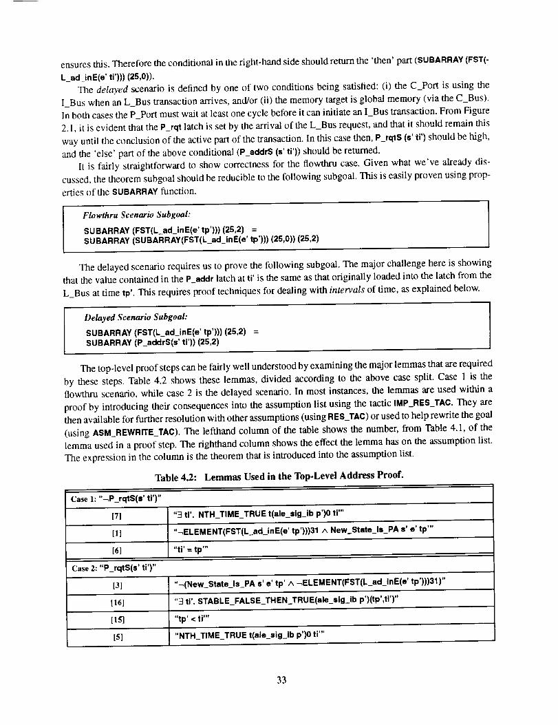
ensuresthis.Thereforetheconditionalinthefight-handsideshouldrealmthe'then'part(SUBARRAY(FST(-
L ad inE(e' ti'))) (25,0)).
The delayed scenario is defined by one of two conditions being satisfied: (i) the C_Port is using the
I Bus when an L_Bus transaction arrives, and/or (ii) the memory target is global memory (via the C_Bus).
In both cases the P_Port must wait at least one cycle before it can initiate an I_Bus transaction. From Figure
2.1, it is evident that the P_rqt latch is set by the arrival of the L_Bus request, and that it should remain this
way until the conclusion of the active part of the transaction. In this case then, P_rqtS (s' ti') should be high,
and the 'else' part of the above conditional (P_addrS ($' ti')) should be returned.
It is fairly straightforward to show correctness for the flowthru case. Given what we've already dis-
cussed, the theorem subgoal should be reducible to the following subgoal. This is easily proven using prop-
erties of the SUBARRAY function.
Flowthru Scenario Subgoal:
SUBARRAY(FST(L_ad_inE(e' tp'))) (25,2) =SUBARRAY (SUBARRAY(FST(L_ad_inE(e' tp'))) (25,0)) (25,2)
The delayed scenario requires us to prove the following subgoal. The major challenge here is showingthat the value contained in the P_addr latch at ti' is the same as that originally loaded into the latch from the
L_Bus at time tp'. This requires proof techniques for dealing with intervals of time, as explained below.
Delayed Scenario Subgoal:
SUBARRAY (FST(k_ad_inE(e' tp'))) (25,2)SUBARRAY (P_addrS(s' ti')) (25,2)
The top-level proof steps can be fairly well understood by examining the major lemmas that are required
by these steps. Table 4.2 shows these lemmas, divided according to the above case split. Case 1 is theflowthru scenario, while case 2 is the delayed scenario. In most instances, the lemmas are used within a
proof by introducing their consequences into the assumption list using the tactic IMP_RES_TAC. They arethen available for further resolution with other assumptions (using RES_TAC) or used to help rewrite the goal
(using ASM_REWRITE_TAC). The iefthand column of the table shows the number, from Table 4.1, of the
lemma used in a proof step. The righthand column shows the effect the lemma has on the assumption list.
The expression in the column is the theorem that is introduced into the assumption list.
Table 4.2: Lemmas Used in the Top-Level Address Proof.
Case 1: "_P_rqtS(a' ti')"
[71 "3 ti'. NTH_TIME_TRUE t(ale_sig_ib p')O ti'"
[1] "-_ELEMENT(FST(L_ad_inE(e' tp')))31 A New_State Is PA s' e' tp'"
161 "ti' = tp'"
Case 2: "P_rqtS(s' ti')"
[31 "-_(New_State Is PA s' e' tp' ^ -_ELEMENT(FST(L_ad_inE(e'tp')))31)"
[161 "q ti'. STABLE_FALSE_THEN_TRUE(ale_sig_ib p')(tp',ti')"
[ 15] "tp' < ti'"
[5] "NTH_TIME_TRUE t(ale_sig_ib p')O ti'"
33

Table 4.2: Lemmas Used in the Top-Level Address Proof.
I [2Ol ] "P_addrS(s' ti')= SUBARRAY (FST(L_ad_inE(e' tp')))(25,0)" [
4.3.1.1 Fiowthru Case
The proof for the flowthru case is fairly short, when given the three lemmas shown in the table. The first
lemma (NTH_IBUS_TRANS_EXISTS [7]) establishes the existence of the t'th I_Bus transaction at time ti', as
shown in the fight-hand column. This 'liveness' property makes it possible to relate the clock- and transac-
tion-level I_Bus variables through the abstraction predicate IBA_PMaster.
The second lemma (P_ROT_FALSE ON Tr IMP_FLOWTHRU_eONDS [1]) establishes the required input
and state conditions, at the beginning of the transaction, associated with the case "_P_rqtS(s' tr)." These con-
ditions, as shown in the right-hand column, are: (i) a logic-zero address bit 31 (indicating a non-CBus tar-
get) and (ii) an FSM next-state value of PA (indicating a free l_Bus).
As seen in Table 4.1, P_RQT_FALSE ON TI' IMP_FLOWTHRU_CONDS[1] states that if P_rqt is low at
time tr, then the conditions in the right-hand column of the above table are implied. There is no way, that
we know of, to prove this lemma directly from the P_Port circuit; instead it was derived from its contrapos-itive, P_RQT_TRUE_ON_TI' [2].
The third lemma in the above table (TRANS_TIMES_EQUAL [6]) is resolved with the previously derived
flowthru conditions to establish the desired equivalence between ti' and tp'. Only a few small steps are
needed to finish the proof for the flowthru case after introducing this lemma.
4.3.1.2 Delayed Case
The proof for the delayed case is also fairly short, when provided with the lemmas shown in Table 4.2.
The first lemma (P_RQT_TRUE_ON_TI'_IMP DELAY_CONDS [3]) establishes the appropriate input and state
initial conditions shown in the right-hand column of the table. Similar to before, this lemma was not proven
directly from the P_Port circuit, but instead derived as the contrapositive of another theorem (P_ROT_.
FALSE_ON_Tr [41).
The second iemma (ALE_SIG_IB_TRUE_AFTER_TP' [16]) is resolved with the delay conditions to estab-
lish the existence of a time (following tp') for which the next I_Bus transaction is initiated.
The third lemma (TI'_AFTER TP' [15]) is then used to establish the strict less-than relationship between
tp' and ti' for the delayed scenario. This is necessary because the value of P_addr should be equal to the
LBus value only after tp', i.e., beginning at the end of the cycle for which the L_Bus request arrived.
The fourth lemma (NEXT_IBUS_TRANS_IS_NTH [5]) is needed to establish that the next I_Bus transac-
tion time, as defined using the second lemma, is in fact the clock-level time for the t'th I_Bus transaction,rather than for some other transaction.
Finally, the fifth lemma (NEW_P_ADDR_STABLE_FROM TP' TO_Tr [20]) establishes the desired rela-
tionship between the P_nddr latch at time ti' and the'L_ad bus at time tp'. As for the flowthru case, only a
few steps are needed to complete the proof once all of these lemmas have been introduced and processed.
4.3.2 Relating the L_Bus and I_Bus Transaction Times
Several of the theorems listed in Table 4.1 are involved with establishing the proper relationships
between the clock-level times of L_Bus transactions and of I_Bus transactions. In studying the expected
operation of the P_Port, it becomes apparent that there should be a one-to-one and onto mapping between
34
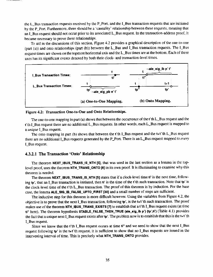
theL_BustransactionrequestsreceivedbytheP_Port,andtheI_BustransactionrequeststhatareinitiatedbytheP_Port.Furthermore,thereshouldbe a "causality' relationship between these requests, meaning that
an I_Bus request should not occur prior to its associated L_Bus request. In the transaction-address proof, it
became necessary to prove these relationships.
To aid in the discussions of this section, Figure 4.2 provides a graphical description of the one-to-one
(part (a)) and onto relationships (part (b)) between the L_Bus and I_Bus transaction requests. The I_Bus
request times are shown on the topmost horizontal axis and the L_Bus times are at the bottom. Each of these
axes has its significant events denoted by both their clock- and transaction-level times.
l_Bus TransactionTimes:
L_Bus Transaction Times:
-_ale_sig_ib p' t't t __.J,,._____.,
; dti'
t
"v"
tp' -_ale_sig_pb e' t'
(a) One-to-One Mapping.
ti "I
t t+l
tp" tp'
(b) Onto Mapping.
Figure 4.2: Transaction One-to-One and Onto Relationships.
The one-to-one mapping in part (a) shows that between the occurrence of the t'th L_Bus request and the
t'th I_Bus request there are no additional L_Bus requests. In other words, each L_Bus request is mapped to
a unique I_Bus request.
The onto mapping in part (b) shows that between the t'th I_Bus request and the t+l 'th L_Bus request
there are no additional I_Bus requests generated by the P_Port. There is an L_Bus request mapped to every
I_Bus request.
4.3.2.1 The Transaction 'Onto' Relalionship
The theorem NEXT_IBUS_TRANS IS NTH [5], that was used in the last section as a lemma in the top-
level proof, uses the theorem NTH_TRANS_ONTO [8] in its own proof. It is illuminating to examine why this
theorem is needed.
The theorem NEXT_IBUS_TRANS IS NTH [5] states that if a clock-level time ti' is the next time, follow-
ing tp', that an I_Bus transaction is initiated, then tr is the time of the t'th such transaction. Note that tp' is
the clock-level time of the t'th L_Bus transaction. The proof of this theorem is by induction. For the base
case, the lemma ALE_SIG_IB FALSE_UPTO_FIRST [30] and a small number of steps are sufficient.
The inductive step for this theorem is more difficult however. Using the variables from Figure 4.2, the
objective is to prove that the next I_Bus transaction, following tp', is the t+l 'th such transaction. The proof
makes use of the theorem NTH_IBUS_TRANS_EXlSTS [7] to establish that a t'th IBus request exists (at time
ti" here). The theorem hypothesis STABLE_FALSE_THEN_TRUE (ale_sig_ib p') (tp',ti') (Table 4.1) provides
the fact that a unique next I_Bus request exists after tp'. The problem now is to establish that this is the t+l 'th
I_Bus request.
Since we know that the t'th I_Bus request occurs at time ti" and we need to show that the next I_Bus
request following tp' is the t+l'th request, it is sufficient to show that no I_Bus requests are issued in the
intervening interval of time. This is precisely what NTH_TRANS_ONTO provides.
35

4.3.2.2 The Transaction 'One-to-One' and 'Causality' Relationships
As seen in Table 4.1, the proof for the theorem NTH_TRANS_ONTO [8] uses as lemmas the theorems
NTH_TRANS ONE TO ONE [91, NTH TRANS_CAUSAL [10], and TRANS_ONTO [12]. Again, it is quite inter-
esting to examine this proof in some of its detail.
The proof for NTH_TRANS_ONTO is split into two cases. The first assumes ti" < tp', while the second
assumes the opposite, or tp' < ti". The first case uses NTH_TRANS_CAUSAL [101and TRANS_ONTO [12] to
help prove the theorem goal directly, and the second case uses NTH_TRANS_ONE TO ONE [9] to create a
contradiction within the assumption list, thereby proving the goal indirectly.
Case l: (1i"< tp'). Again using the variables from Figure 4.2, the theorem hypotheses, after some manip-
ulation, provide us the fact that no L_Bus requests arrive between the clock-level times tp" and tp'. The the-
orem NTH_TRANS_CAUSAL [10] is resolved with the theorem hypotheses to provide the fact tp" < ti", which
is then processed to establish that no L_Bus requests arrive between the times tr' and tp', a condition match-
ing the last precondition of TRANS_ONTO [12].
As seen in Table 4.1, TRANS_ONTO [121 is a somewhat weaker version of NTH_TRANS_ONTO [8]. The
major difference between the two is that one of the preconditions for TRANS_ONTO [12] states that tp' marks
the time for the next L_Bus transaction, following ti", while for NTH_TRANS_ONTO [8], tp' corresponds to
the t+1 'th L_Bus transaction, but without regard to its relationship to ti". The stronger precondition within
TRANS_ONTO [12] permits it to be proven directly from the P_Port circuit description, in contrast to the sit-
uation for NTH_TRANS_ONTO [8].
The precondition for TRANS_ONTO [12] is just weak enough however, to match the previously-discussed
conditions within the assumption list for the case-1 goal. An application of IMP_RES_TAC with this theorem,
and some minor proof steps, are sufficient to solve the goal.
Case 2: (tp' < tr'). As seen in Figure 4.2, this is a contradictory scenario. From the theorem hypotheses
we can obtain the relationship tp" < tp' to go along with our assumption tp' < ti"; that is, tp' falls within the
interval (tp", ti"], which includes the time ti" but not tp". The theorem NTH_TRANS_ONE TO ONE [9] states
that, given suitable preconditions (which are contained in the assumption list), there are no L_Bus _ansac-
tion requests occurring within this interval. However, this contradicts other conditions within the assump-
tion list which state that an L_Bus request does arrive at the time tp' within the interval.
4.3.2.3 Discussion
The five theorems NTH_TRANS_ONTO [8], NTH_TRANS_ONE TO ONE [9], NTH_TRANS_CAUSAL [10],
TRANS_ONE TO ONE [11], and TRANS_ONTO [12] establish sufficient relationships between the L_Bus
transaction requests and the I_Bus transaction requests to achieve a transaction-address proof. Discovering,
and proving, this set of theorems was a major undertaking and required a significant amount of time and
effort. But, having gone through the process once, we are now in a position to investigate ways to make
future proofs of this type easier.
Two approaches to handle problems of this type make sense. One approach is to continue on with the
current methods, but seek to refine them in order to discover a minimal set of theorems necessary to be
proved. By beginning with what we have already learned under this task, such an approach would be more
efficient on future efforts similar to this one.
Another approach, that we believe has more promise, is to make better use of the notion of 'precondi-
tions.' In particular, the idea may be transferable from the pre-post interpreter model into the abstraction
predicates. So called 'abstraction preconditions' could permit one to postulate the existence of a one-to-one
and onto relationship between appropriate transactions prior to the transaction under consideration. In such
36

ascenario,thenextI_Bustransaction,forexample,couldeasilybeshowntobethet+l 'th such transaction,
without the need to establish, by proof, any facts about prior transaction behavior (which is what NTH_TRAN-
S_ONTO [8] does).In other words, abstraction preconditions could permit theorems such as NEXT_IBUS_TRANS IS NTH [5]
to be proven much more easily than is now possible. The theorem-proving price for this is the set of proof
obligations necessaryto propagate the preconditions onto the next transaction. This may be no worse, how-
ever, than the theorems TRANS_ONE TO ONE [11] and TRANS_ONTO [12] already required. We plan to
investigate abstraction preconditions during our work under Task 12 of this contract. Longer-term work
might include developing a generic theory to automatically handle some of the required proof infrastructure.
4.3.3 Theorem Proving Over Intervals
In order to prove the theorems in the previous sections it was necessary to reason over intervals. For
example, the proof for TRANS_ONTO [12] requires reasoning about two intervals. Again using the variables
within Figure 4.2, TRANS_ONTO [12] states that between the clock-level time ti" and the next occurrence of
an L_Bus transaction request, there are no intervening I_Bus transaction requests sourced by the P_Port.
Theorems [13] and [14] of Table 4.1 provide the sufficient conditions for the two intervals involved.The theorem NEW_STATE PD FROM TI' TO T'SACK [14] states that the P_Port FSM has an output of
d_state in the clock-level interval beginning after ti' and ending with t'sack (see Figure 4.1 for these times).
From Figure 2.1 it is clear that none of I_male_, I_rale_, nor I__¢ale_ call be active low during this time since
this requires a mutually exclusive FSM output of a_=tate. Therefore, the I_Bus transaction-request signal
ale_sig_ib p' must be inactive-low during this interval.
The theorem NEW_P_RQT_FALSE_FROM_T'SACK TO TP'SUC [13] states that, in the interval beginning
with t'sack and ending with tp'suc, the P_rqt latch output value is low. As seen from Figure 2.1, this is suf-
ficient to ensure that ale_sig_ib p' is low during this particular interval.
Appending these two subintervals together creates the interval of interest to the TRANS_ONTO [12] the-
orem and goes a long way towards achieving the proof. In addition to these two interval theorems, the the-
orems numbered [20], [21], [22], [23], [30], and [31] all establish facts about state or output variables during
particular intervals of time.The interval theorems dealing with the clock-level times preceding the first L_Bus transaction request
(numbers [30] and [31]) are easily proven. The others, however, are not as easy to prove, and required us to
develop a new technique to handle them.Induction is the natural choice for proving theorems of this sort, but, unfortunately, it cannot be directly
applied here. The problem is that the lower bound of the interval (being non-zero) cannot be properly han-
dled in the induction step. For example, consider an interval of time defined for the variable t' as follows: tp'
<_t' ^ t' < ti'. In the induction step (we're inducting on t') the theorem precondition, tp' < SUC t' ^ SUC t' <
ti', is entered into the assumption list where it must (in a typical induction) be resolved with the precondition
of the inductive hypothesis. However, in the inductive hypothesis, the precondition reads: tp' <_t' ^ t' _<ti'.
While the second conjunct can be inferred from the theorem precondition, the first conjunct (tp' <_t') cannot
be, and the proof comes to a unsuccessful halt.To solve interval-induction problems, we induct over the offsetinto the interval rather than over all time.
This creates a theorem that, when properly specialized, can be used to prove the theorem of interest. Inter-
val-induction proofs are thus a two-step procedure. The theorems in Table 4.1 do not reflect this; we have
only entered the 'finished' theorem statements there.
37

Togettheflavorof thistwo-stepprocess,thefollowing(partial)theoremstatementis thefirststepofthe theorem NEW_STATE_PD_FALSE_FROM_TP' TO Tr [23]:
OFFSETNEW_STATE PD .FALSE_FROM_TP'_TO_TI':
I. V u. NTH_TIME_TRUE t (ale_sig._pbe') 0 tp' :9STABLE_FALSE (ale_sig_ib p') (tp', ti'-l)
((tp'+u') < ti') :_-_New_State Is PD $' e' (tp'+u')
The variable u' in this theorem statement is the offset into the interval, that begins at time tp' and ends
at ti'. To achieve the proof for the finished theorem, this theorem is used with u' specialized to t'-tp'. Aftersome algebraic manipulations the finished theorem results.
We used this two-step approach to prove most of the interval theorems for the P_Port. We were never
happy with this approach, however, and towards the end of the task we implemented a new induction tactic
that handles interval inductions directly. This tactic, called RANGE_INDUCT_TAC, when applied to a goal,produces two simpler subgoals as demonstrated here.
Goal: "Vt. a_<t :9 t_<b :9 Pt"
RANGE_INDUCT_TAC
Subgoals: "P a"("a_<b"]
"P (SUC (a + u))"[ "P (a. u)" ][ "(sue (a+ u))< b"]["(a + u)< b"]
This tactic tests out well on small examples, but hasn't been used on any major proofs within the P_Port
yet. Part of our Task 12 work will continue the development of this approach.
4.4 Transaction Block-Size Verification
In this section we provide a brief description of the partially-completed block-size verification. The
emphasis of this section is on those aspects of the block-size problem that distinguish it from the addressverification problem.
The address correctness proof, by itself, represents a significant percentage of the work needed to com-
plete the entire P_Port proof. This is because of the large number of theorems developed for the address
proof that can be reused for the other variables. The block-size verification does require significant new the-
orem development however. The address verification principally dealt with the time interval between tp' and
tr, whereas the block-size verification also deals with the intervals tr-t'rdyo, t'rdyO--t'rdyl, and so on.
An interesting aspect of the PIU PPort, from a modeling and verification point of view, is the way that
block-size information is represented differently by the protocols of the two interface buses. On the L_Bus
side the block size is contained within the two address bits L_ad[1:0] during the first clock cycle of the trans-
action (at tp'). From Figure 2. l, it would appear that the block size transmitted onto the I_Bus is this same
38

pair of bits on I_ad[25:24]. However, these bits are not used by the slave ports of the PIU; instead the I_Bus
block-size information is defined by the behavior of the P_Port control signal I_last_.
Figure 4.3 shows how I_last is interpreted. Informally, a block size of one word, which is represented
by a block-size 'value' of 0, is defined by an I_last_ value of LO during the first word interval. A two-word
block is defined by an I_last_ value of HI during the first word and LO during the second. The other block
sizes follow this pattern. The timing diagram in the figure is the typical way that this type of behavior is
represented and understood by designers. The HOL representation at the right is quite readable however,
and has eliminated the ambiguity found in the timing diagram, particularly with regard to the precise cycle
that I last must go LO. The HOL predicate STABLE_LO f 01 ,t2) is true if and only if the signal f has the value
LO for all-times between tl and t2, including the end points. The signal bsig I_last_O p' maps clock-level
time, t', to the phase-B value of the 2-tuple I_last_O (p' t'). (bsig s f is defined as _. t. BSel (s (f t)).)
Block Informal SpecificationSize
I_last_
2
ti'
av
t'rdy0 t'rdyl t'rdy2 t'rdy3
HOL Specification
STABLE_LO (bsig I_lut_O p')( ti'+l, t'rdy0)
STABLE_HI (bsig l_last_O p') (ti'+1, t'rdy0) ^STABLE_LO (bsig l_last_O p')( t'rdy0+1, t'rdyl)
STABLE_HI (bsig l_last_O p') (ti'+l, t'rdyl) ^STABLE_LO (bsig l_last_O p')( t'rdyl+1, t'rdy2)
STABLE_HI (bsig l_last_O p') (ti'+1, t'rdy2) ^STABLE_LO (bsig l_last_O p')( t'rdy2+1, t'rdy3)
Figure 4.3: Informal and HOL Definitions for the Transaction Block Size.
When discounting the proof infrastructure required by both the address and block-size verifications, the
block-size proof is seen to be more difficult than the address proof. In addition to the greater inherent com-
plexity of the block-size abstraction, the block-size hardware implementation is also more complex. As seen
in Figure 2.1, the I_last_ output is sourced by the P_size counter that is controlled by two inputs: 'load' and
'down,' sourced by the latches P_load and P_down, respectively. P_load is itself controlled by the P_rqt
latch, and P_down is controlled by both I_srcb/_ and the FSM output d_state. In addition, I_last_ is driven by
a tri-state driver that is controlled by the FSM output hlda_.
The block-size proof is split into four cases, distinguished by the values of the 2-bit block-size field,
L ad[1:0]. At this time, we have proven the first two cases (for block-size values o and 1) and have completed
n_ost of the theorems for the third case. We have also proven the top-level correctness theorem for the block
size by temporarily assuming lemmas for the third and fourth case. This proof will be completed as part of
Task 12.
39

Table 4.3 summarizes six of the theorems proven for the block-size-0 case. The theorem numbers arecontinued from those in Table 4.1.
Table 4.3: Major Theorems Used in the First Block-Size Proof.
DescriptionNo.
[35] I_LAST_FOR_BLOCK SIZE 0
"... D (SUBARRAY(SND(L_adJnE(e' tp')))(1,0) = WORDN 1 0)
STABLE_TRUE_THEN_FALSE(bsig I srdy_E e')(tl'+l,t'rdy0)
STABLE_LO(b$1g I_last_O p')(U'+l,t'rdy0)"Theorems used: [10] [14] [36] [37] [39]
[36] P_SIZE_STABLE_FROM TP' TO T'RDY0
"... _ STABLE_TRUE_THEN_FALSE(bsig I_srdy_E e'Xtl'+l,t'rdy0) _ (tp'+l _ t') _ (t'_< t'rdy0)(P_sizeS(s' t') ,, SUBARRAY(SND(L_ad_InE(e' tp'))X1,0))"
Theorems used: [37] [38] [39]
[37] P_DOWN_STABLE_FALSE_THEN_TRUE_FROM_TP' TO T'RDY0
"... _ STABLE_TRUE_THEN_FALSE(b_ig I_srdy_E e')(tl'+l,t'rdy0))
D STABLE_FALSE_THEN_TRUE(Lu'. P_downS(s' u'))(tp'+l,t'rdy0+l)"Theorems used: [5] [10] [14] [23] [39]
[38] P_LOAD_TRUE_THEN_STABLE_FALSE_FROM_TP'_TO_T,SACK
"... _ STABLE_FALSE(Sack_SIg_Is_TRUE t' e')(tr,t'uck.1)
D TRUE_THEN_STABLE_FALSE(_u'. P_loadS(s' u'))(tp',t'sack)"Theorems used: [5] [10] [22] [40]
[39] SAC K_S[G_FALS E_DURING_DATA_0
"... _ STABLE_TRUE.THEN_FALSE(bslg I_erdy_E e')(tr+l,t'rdy0)STABLE_FALSE(Sack_SIg_Is_TRUE s' e')(ti',t'rdyO-1)"
Theorems used: [251
[40] NE W_P RQT_TRUE_FROM_TI'_TO_T'SACK
"... D STABLE_FALSE(Sack_Sig_Is_TRUE .' s')(ti',t'uck-1) _ (U' _<t')(t' < t'sack) _ Nsw_P_Rqt_Is_TRUE e' e' t' "
Theorems used: [33]
The first theorem, I_LAST FOR_BLOCK_SIZE_0 [35], establishes the desired conditions for I_last_,
matching the block-size-0 specification shown in Figure 4.3. (WORON m n is the re+l-bit bit-vector corre-
sponding to the natural number n.) In the top-level block-size proof, the first precondition for this theorem
is provided automatically by the case split mentioned above. The second precondition is obtained from the
constraints placed on I_Bus slave ports. The abstraction predicate IB_PMuter, shown in Section 4.2.2, con-
tains these constraints, which are informally: (i) the slave port will transmit an active-low I_srdy_ sometime
after ti', and (ii) if lima_ is inactive-high when the slave port transmits an active-low I_sr__, then the slave
will transmit another low I_srdy_ sometime in the future. These two constraints are part of the slave portionof the I_Bus protocol.
A stable-LO I_lut_ requires three conditions: (i) a P_size value of zero (FF), (ii) a low P_down value,
and (iii) a high hldn_ value. The need for conditions (i) and (iii) is clear, since the P_si_ 'zero' output and
hlda_ are the source and enable for the I_lul_ ll'i-state buffer, respectively. Condition (ii) is needed because,
although not evident from Figure 2.1, the V_size counter output is a function of P_down. Condition (i) is
provided by the theorem P_SIZE_STABLE_FROM TP' TO_T'RDY0 [36]; condition (ii) is provided by
P_OOWN_STABLE_FALSE_THEN_TRUE_FROM TP' TO T'ROY0[37]; and condition (iii) is obtained from the
combination SACK_SIG_FALSE_DURING_DATA_0 [39] and NEW_STATE PD FROM TI' TO T'SACK[14].
40
The remaining theorem dependencies shown in Table 4.3 are fairly straightforward. The interested
reader is referred to [Fur93c] for the full details of the partially-completed block-size proof.
4.5 Discussion
In this section we describe the current status of the PIU requirements verification and discuss the veri-
fication process itself.
4.5.1 Current Status
The only transaction-level verification attempted so far has been in the P_Port for transactions initiated
by the local processor. As explained in this section, the proof for the transaction-level address is finished
and the proof for the block size is more than half completed. The remaining transaction-level variables are
the data outputs, for both writes and reads, the byte-enable outputs, the three opcode outputs, and the two
next-state variables.
We believe that the work completed so far represents approximately 80-90% of the P_Port verification.
Most of the 'proof infrastructure' must be completed for the first proof, but can then be reused for the other
proofs. In addition, the other variables have relatively simple abstractions, making them inherently easier to
handle, than the block size for example. For instance, the byte enables and data outputs all have flowthru
behavior. The L_Bus opcode proof will reuse several of the higher-level theorems proven for the block size
proof.In the address verification, all the theorems were proven except for one that was assumed. Its proof
appears to be tricky, but assuming it for now was considered to be low risk, in light of the amount of uncer-
tainty present in other areas of the P_Port verification. A few 'theorems' were also assumed in the block-
size work done so far--these will be cleaned up as the development of the proof continues.
4.5.2 The Transaction-Level Verification Process
A common criticism of the HOL system is the large amount of low-level proof detail that must be pro-
vided by the user. As seen in [Fur93c] there is a tremendous amount of detail required for the proofs com-
pleted thus far, and many of these proofs were extremely tedious and time-consuming. However, it has been
our experience on this task that higher-level theorem-proving issues have been just as significant a problem
as the individual proof constructions.
When we began the transaction-level verification, we had a pre-post interpreter model that had been
tested on only a few small examples. As we progressed, we discovered that our specification methods were
under seemingly constant revision and that new proof techniques had to be developed in some cases. Getting
into the heart of the address proof, we encountered places where it was unclear which among several differ-
ent paths should be taken to solve certain goals. This is particularly true for the theorems, relating the L_Bus
and I_Bus transaction times, that were explained in Section 4.3.2.
Many of these problems will not exist for the next port that we address. A key objective in this and future
work will be to use what we have learned here and to generalize our techniques as much as possible. Ulti-
mately, we hope to develop a generic theory for transactions comparable to the generic interpreter theory.
We developed our temporal logic theory (templogic_deJ) as part of this task. Our main objective with it
was to provide meaningful specifications, hence it contains, for example, both of the predicates STABLE_-
FALSE_THEN_TRUE and STABLE LO THEN_HI, for types ":boor' and ":wire" respectively. However, we are
not completely satisfied with what we have now, and see a need for much more work in defining a truly good
41

setof temporal-logicprimitivesfor modelingthebusprotocolsassociatedwith thePIU,andsimilarsub-systems.
Thesamecommentsmadeconcerningourwordn_deftheory in Section 3.3.2 are reiterated here. We
need a richer theory with, for example, built-in arithmetic tactics to prove automatically such trivially-true
facts as -(WORDN 1 2 = WORDN 1 3). Such a theory would have sped up considerably the proofs dealingwith the P_size counter in the block-size verification.
42

5 Conclusions
We have successfully completed significant portions of the PIU verification using techniques that
extend the current state-of-the-art in interpreter modeling and verification. In this section we discuss: (a)
the clock-level verification, (b) the partially-completed transaction-level verification, (c) design issues, and
(d) future work.
5.1 Clock-Level Verification
Modeling and verification concepts from the generic interpreter theory were used to great benefit in the
PIU clock-level verification. By restricting the abstraction between the clock level and the underlying gate
level to structural only, the clock-level proofs were extremely straightforward to construct. A single (suit-
ably customized) 3-line tactic was sufficient to verify the majority of the 170 next-state and 60 output vari-
ables. In addition, by capturing the complete clock-level behavior within a single instruction, the amount of
required theorem proving was minimized.
The clock-level verification took approximately three man-months for the 230 state and output proofs.
However, much of this time was spent on activities that would not be acceptable in a mature hardware devel-
opment process. The two problem sources for these proofs were: (a) incorrect, complex specifications and
(b) difficult design constructs. Future work to address these problems is discussed below.
A behavioral version of the implementation structure (such as the clock level) is an important level in a
specification hierarchy because: (a) as discussed above, it is easy to construct proofs for and (b) the CPU
requirements for these proofs can be high (several hours for some of the PIU variables). Because the proof
construction for this level is so easy, human interaction is minimal. Long proof (CPU) times may be toler-
able in such scenarios, in contrast to the difficult transaction-level proofs, for example, where the level of
human interaction is necessarily higher. Many of our transaction-level theorems would not have been
proved had the clock level not existed.
5.2 Transaction-Level Verification
Transaction-level verification is extremely hard. To our knowledge, we are the first to attempt proofs at
this level, and the corresponding lack of experience within the theorem-proving community has contributed
to our workload. The impact that our lessons learned should have on future work is summarized below.
More fundamentally, transaction-level verification is hard because of the complex relationships existing
between the transaction-level variables and the underlying clock-level variables. In other previous work,
primarily with non-pipelined microprocessors, concrete variables were mapped to the abstract level only at
the boundaries of the abstract operations. In this 'point abstraction' approach the mappings are simple.
In contrast, the 'interval abstraction' that is necessary for the transaction level maps concrete variable
intervals to the abstract, transaction level. This abstraction is implemented using a temporal logic that we
have developed specifically for this purpose. After the early steps in a transaction-level proof, these tempo-
ral-logic formulas become, in effect, the 'specification' for the underlying clock-level state machine. Com-
pleting these proofs in HOL is a tedious and time-consuming job.
In this task we have completed approximately 80-90% of the P_Port transaction-level verification, rep-
resenting approximately three man-months of effort. Of this time, all but two weeks were devoted to the
proof for the first P_Port transaction-level variable (the address). Even though the block size has a much
more complicated abstraction, only two weeks were needed to complete roughly 75% of the block-size ver-
ification. Virtually all of the proof 'infrastructure' is now completed, and the proofs for the remaining vari-
ables are expected to be completed much faster.
43
5.3 Design Issues
In contrast to the previous task (Task 9), that was performed in parallel with parts of the PIU design and
uncovered some latent design mistakes, this task has not discovered any serious design flaws. This is not to
say that mistakes don't exist, only that the partially-completed transaction-level verification has not discov-
ered any to date. However, we have found some design weaknesses that make the design more difficult to
verify and, in some cases, have the potential to cause future problems.
Within the P_Port the control logic is distributed among several latches and gates. This burdened the
transaction-level proof because each of these latches generally required one or more interval-induction the-
orems to be proved. This is not merely a theorem-proving issue, since a high level of proof effort corre-
sponds directly to a high level of human reasoning necessary to even comprehend the design. Future
'verification-sensitive' designs should try to centralize this type of control logic within a single statemachine.
The use of level-sensitive devices, such as latches, and other 'complex output' devices also added to the
proof burden in the P_Port verification. The output expressions for latches contain the latch input expres-
sions, in addition to the latch state, making them cumbersome to deal with. In addition, a counter in the
P_Port had its decrementer on its output side rather than its input side. Thus, even though the counter is an
edge-sensitive device, its output expression is complicated by the presence of the 'count-down' input. These
types of structures, when taken together, added significantly to the PPort verification burden. Where prac-
tical, they should be avoided in future verification-sensitive designs.
Finally, it appears that the designers' lack of an explicit I_Bus protocol specification to design from has
led to some increased complexity within the PPort. As explained in the Specification Report [Fur93a],
P_Port correctness depends on C_Port behavior that is nontrivial to verify and, perhaps even worse, was not
even documented. Without clear interface specifications it is much too easy, at best, to add unnecessary com-
plexity to a design and, at worst, to make an unwarranted assumption that results in a fatal bug. As others
before us, we strongly advocate the use of rigorous interface specifications in subsystem designs, to promote
both design correctness and design elegance (and ease of verification).
5.4 Future Work
While we have demonstrated how transaction-level interpreters may be verified, much work remains to
make future tasks like this efficient, and, in fact, practical.
To begin, future design verifications should make greater use of automation than we have applied here.
As explained in Section 3.4, the gate- to clock-level verification problem is so straightforward that it is con-
ceivable to generate clock-level models mechanically from their gate-level counterparts, and then to auto-
matically construct the necessary theorem statements and tactics to prove the clock-level correctness.
Modest design constraints, such as requiring the use of pre-verified bus modules rather than individual tri-
state buffers, can be used to address difficult areas within the gate-to-clock boundary.
This approach is especially attractive because it can serve two different communities having an interest
in theorem proving. For the 'design process improvement' community it provides the speedy generation of
clock-level behavioral models for use higher up in the verification hierarchy. The clock-level proofs can be
executed in the background, or overnight. The 'safety-' and 'security-critical' communities are served by
the full rigor of the formal clock-level correctness proofs that are eventually produced.
The requirements verification process needs significant advances to make these verifications practical.
Problems exist on at least two levels here. The detailed circuit-related theorems of the P_Port were
extremely tedious and time-consuming to prove. Yet most of these proofs were similar in form, with the
major differences being in the particular state and input variables used. With more experience it should be
44

possibleto makethesetypesof proofsmoresystematicandefficient.Increasingthelevelof automation,usingtheinterfacelanguageML,isalmostalwaysagoodideaandshouldbe investigated. Another approach
deserving strong consideration is the embedding of 'pseudo formal' techniques, such as model checking
[McM93], into the prover. The work being done to combine HOL with the VOSS trajectory evaluation tool
[Joy93] is a noteworthy example of this approach.
Another area deserving attention is the possible greater use of preconditions. In particular, as explained
in Section 4.3.2, using 'abstraction preconditions' might have saved a significant amount of work in the
P_Port verification. The beneficial aspect to preconditions is their ability to keep the theorem-proving atten-
tion focused on the current operation under consideration - prior operation behavior can be ignored. Some
of the hardest proofs in the P_Port verification were the ones that spanned multiple operations (transactions).
As we complete the P_Port verification and move on to the other PIU ports, we will investigate some
of these ideas further.
45

6 References
[Cam86]
[Chu40]
[Con86]
[Fur92]
[Fur93a]
[Fur93b]
[Fur93c]
[Gor79]
[Gor86]
[Gor88]
[Int89]
[Joy93]
[McM93]
[Win90]
A. Camilleri, M. Gordon, and T. Melham, "Hardware Verification using Higher-Order Logic,"in D. Borrione (editor), From HDL Descriptions to Guaranteed Correct Circuit Designs, North-Holland, 1986.
A. Church, "A Formulation of the Simple Theory of Types," Journal of Symbolic Logic, Vol. 5,1940.
R.L. Constable, Implementing Mathematics with the NUPRL Proof Development System, Pren-tice Hall, 1986.
D.A. Fura, P.J. Windley, and G.C. Cohen, "Formal Design Specification of a Processor Inter-face Unit," NASA Contractor Report 189698, November 1992.
D.A. Fura, P.J. Windley, and G.C. Cohen, "Towards the Formal Specification of a Processor In-
terface Unit," NASA Contractor Report 4521, 1993.
D.A. Fura, P.J. Windley, and G.C. Cohen, "Towards the Formal Specification of a Processor In-
terface Unit - HOL Listings," NASA Contractor Report 191465, 1993.
D.A. Fura, P.J. Windley, and G.C. Cohen, "Towards the Formal Verification of a Processor In-
terface Unit - HOL Listings," NASA Contractor Report 191466, 1993.
M. Gordon, R. Milner, and C. Wadsworth, Edinburgh LCF: A Mechanized Logic of Computa-
tion, Lecture Notes in Computer Science, Vol. 78, Springer-Verlag, 1979.
M. Gordon, "Why higher-order logic is a good formalism for specifying and verifying hard-
ware," in G.J. Milne and P.A. Subrahmanyam (editors), FormalAspects of VLSIDesign, Elsevi-er Science Publishers, 1986.
M.J.C. Gordon, "HOL: A proof generating system for higher-order logic," in G. Birtwistle and
P.A Subrahmanyam (editors), VLSI Specification, Verification, and Synthesis, Kluwer AcademicPress, 1988.
Intel Corporation, 80960MC Hardware Designer's Reference Manual, June 1989.
J.J. Joyce and C.H. Seger, "Linking BDD-Based Symbolic Evaluation to Interactive Theorem-
Proving," in Proceedings of the 30th Design Automation Conference, IEEE Computer SocietyPress, June 1993.
K.L. McMillan, Symbolic Model Checking, Kluwer Academic Publishers, 1993.
P.J. Windley, The Formal Verification of Generic Interpreters, Ph.D. thesis and Research ReportCSE-90-22, Division of Computer Science, University of California, Davis, July 1990.
46

Appendix A: HOL Overview
HOL is a general theorem proving system developed at the University of Cambridge [Gor88] [Cam86]
that is based on Church's theory of simple types, or higher order logic [Chu40]. Church developed higher
order logic as a foundation for mathematics, but it can be used for describing and reasoning about compu-
tational systems of all kinds. Higher order logic is similar to the more familiar predicate logic, but allows
quantification over predicates and functions, not just variables, allowing more general systems to be
described.
HOL grew out of Robin Milner's LCF theorem prover [Gor79] and is similar to other LCF progeny such
as NUPRL [Con86]. Because HOL is the theorem proving environment used in the body of this work, we
describe it in more detail. This description is taken from [Win90], with some additions to support the dis-
cussions of this report.HOL's proof style can be tailored to the individual user, but most users find it convenient to work in a
goal-directed fashion. HOL is a tactic-based theorem prover. A tactic breaks a goal into one or more sub-
goals and provides a justification for the goal reduction in the form of an inference rule. Tactics performtasks such as induction, rewriting, and case analysis. At the same time, HOL allows forward inference, and
many proofs are a combination of forward and backward proof styles. Any theorem-proving strategy a user
employs in connection with HOL is checked for soundness, eliminating the possibility of incorrect proofs.
HOL provides a metalanguage, ML, for programming and extending the theorem prover. Using ML,
tactics can be put together to form more powerful tactics, new tactics can be written, and theorems can be
combined into new theories for later use. The metalanguage makes the HOL verification system extremely
flexible.
In HOL, all proofs, even tactic-based proofs, are eventually reduced to the application of inference
rules. Most nontrivial proofs require large numbers of inferences. Proofs of large devices such as micropro-
cessors can take many millions of inference steps. In a proof containing millions of steps, what kind of con-
fidence do we have that the proof is correct? One of the most important features of HOL is that it is secure,
meaning that new theorems can only be created in a controlled manner. HOL is based on five primitive axi-
oms and eight primitive inference rules. All high-level inference rules and tactics do their work through
some combination of the primitive inference rules. Because the entire proof can be reduced to one using
only eight primitive inference rules and five primitive axioms, an independent proof-checking program
could check the proof syntactically.
A.1 The Language
The object language of HOL is described in this section. We will discuss HOL's terms and types.
Terms. All HOL expressions are made up of terms. There are four kinds of terms in HOL: variables,
constants, function applications, and abstractions (lambda expressions). Variables and constants are denoted
by any sequence of letters, digits, underlines, and primes starting with a letter. Constants are distinguished
in the logic; any identifier that is not a distinguished constant is taken to be a variable. Constants and vari-
ables can have any finite arity, not just 0, and, thus, can represent functions as well.
Function application is denoted by juxtaposition, resulting in a prefix syntax. Thus, a term of the form
"tl t,7."is an application of the operator tl to the operand t2. The term's value is the result of applying tl to t2.An abstraction denotes a function and has the form "_.x. t." An abstraction "X x. t" has two parts: the
bound variable x and the body of the abstraction t. It represents a function, t, such that "f(x) = t." For example,
"Xy. 2,y" denotes a function on numbers that doubles its argument.
47

Constantscanbelongto twospecialsyntacticclasses.Constantsof arity2canbedeclared to be infix.
Infix operators ate written: "rand1 op rand2" instead of in the usual prefix form: "op rand1 rand2." TableA. 1 shows several of HOL's built-in infix operators.
Constants can also belong to another special class called binders. A familiar example of a binder is V.
If c is a binder, then the term "e x. t" (where x is a variable) is written as shorthand for the term "e(k x. t)."Table A.2 shows several of HOUs built-in binders.
Operator
A
Table A.I: HOL Infix Operators.
Application Meaning
tl = t2 tl equals t2
tl, t2 the pair tl and t2
tl A t2 tl andt2
v tl vt2 tlort2
tl _ t2 tl implies t2
Table A.2: HOL Binders.
Binder Application Meaning
V Vx.t for all x, t
3 q x. t there exists an x such that t
e e x. t choose an x such that t is true
In addition to the infix constants and binders, HOL has a conditional statement that is written
"a _ b I c," meaning "ifa then b else c."
Types. HOL is strongly typed to avoid Russell's paradox and others like it. Russell's paradox occurs in
a high order logic when one can define a predicate that leads to a contradiction. Specifically, suppose that
we define P as P(x) = -at(x), where -_ denotes negation. P is true when its argument applied to itself is false.
Applying P to itself leads to a contradiction since P(P) = _p(p) (i.e., true = false). This kind of paradox can
be prevented by typing since, in a typed system, the type of P would never allow it to be applied to itself.
Every term in HOL is typed according to the folll3wing recursive rules:
a. Each constant or variable has a fixed type.
b. If x has type a and t has type 15,the abstraction _. x. t has the type (ct --> 15).
c. If t has the type (ct _ 15)and u has the type a, the application t u has the type 15.
Types in HOL are built from type variables and type operators. 'l_ype variables are denoted by a sequence
of asterisks (,) followed by a (possibly empty) sequence of letters and digits. Thus, ,, ***, and ,ab2 are all
48

valid typevariables.All typevariablesareuniversallyquantifiedimplicitly,yieldingtypepolymorphicexpressions.
Typeoperatorsconstructnewtypesfromexistingtypes.Eachtypeoperatorhasa name(denotedbyasequenceof lettersanddigitsbeginningwitha letter)andanarity.If at..... an are types and op is a type
operator of arity n, then (or1..... czn)op is a type. Note that type operators are postfix while normal function
application is prefix or infix. A type operator of arity 0 is a type constant.HOL has several built-in types that are listed in Table A.3. The type operators bool, ind, and fun are
primitive. HOL has a special syntax that allows (,,**)prod to be written as (* # **), (*,**)sum to be written
as (. + **), and (,,**)fun to be written as (* -_ **).
Table A.3: HOL Type Operators.
Operator A rity Meaning
bool 0 booleans
ind 0 individuals
hum 0 natural numbers
(*)list 1 lists of type *
(*,**)prod 2 products of * and **
(*,**)sum 2 coproducts of * and **
(*,**)tun 2 functions from * to **
A.2 The Proof System
HOL is not an automated theorem prover, but is more than simply a proof checker, falling somwhere
between these two extremes. HOL has several features that contribute to its use as a verification environ-
ment:a. Several built-in theories, including booleans, individuals, numbers, products, sums, lists, and
trees. These theories contain the five axioms that form the basis of higher order logic, as well
as a large number of theorems that follow from them.b. Rules of inference for higher order logic. These rules contain not only the eight basic rules of
inference from higher order logic, but also a large body of derived inference rules that allow
proofs to proceed using larger steps. The HOL system has rules that implement the standardintroduction and elimination rules for Predicate Calculus as well as specialized rules for rewrit-
ing terms.c. A collection of tactics. Examples of tactics include: REWRITE_TAC which rewrites a goal
according to previously proven theorems; ASM_REWRITE_TAC which rewrites using the
assumption list in addition to specified theorems; GEN TAC which removes universally quanti-fied variables from the front of terms; CONJ_TAC which splits a conjunction into two separate
subgoals; ASSUME TACwhich introduces a previously proven theorem into the assumption list;
IMP RES TAC which resolves an implication-style theorem with the assumption list; and
INDUCT_THEN which performs a case split on a variable with an 'enumerated' type.
49

do
e.
A proof management system that keeps track of the state of an interactive proof session.
A metalanguage, ML, for programming and extending the theorem prover. Using the metalan-
guage, tactics can be put together to form more powerful tactics, new tactics can be written, and
theorems can be aggregated to form theories for later use. The metalanguage makes the verifi-cation system extremely flexible.
50


REPORT DOCUMENTATION PAGE For,.A_,_o_No. 0704-0188
Pulbhc reporlm 9 burdqm for thi ,.._;.._.c... od ;,.-_,,.;.;.,_, Is w;;,..---'_¢l lo avorl_e 1 hour p_ re_oOnlm. _nolu¢lmg the lime toq revmwmg .ntmactmns. seat=brag oxmm 9 ¢iEa sources.
ilathenng and enlmtmnihg the _ needed, and ¢om_nng Im¢l rev_wmg the ¢_llect_on ot *nfomvll_,.. Send corr, rrontl reg_'dmg Ihrl I)¢J_le/1 IlhrP.IIO Of any olhl! _ el lhll
colecllon d irdorwlltlorq,ilholu¢lil_lSt_il(_S for rgdgcmg lhMI b_fden, to Washington hte_uarte_ Sorvm, Dwe_lorae toq In|eriCson OqDDrll_lOrlsand Rq_orls. 121 =; Jellemon Dmml
_l._ay, Suite 12'0_, k,rTm,_on, VA 22202-4302. _ _o the O_m el Msna_t and Bu,o_. Pemef_ork R_Jua_o_, Pm,_ (0704-01U}. W_i_o.n. DE: 205O3.
1. AGENCY USE ONLY (L44w b_) 2. nePOm" DATe 3. REPORT TYPE AND DATES COVERED
December 1993 Contractor Report
4, TITLE AND SUu;vvI.E
Towards the Formal Verification of the Requirements and Design of a ProcessorInterface Unit
s. AUTHOR(S)
David A. Fura, Phillip J. Windley', and Gerald C. Cohen
7. PERFORMING ORGANIZATION NAME(S) AND ADORESS_ES)
Boeing Defense & Space Group
P.O. Box 3707, M/S 4C-70
Seattle, WA 98124-2207
9. SPONSORING / MONITORING AOENCY NAME(S) AND ADORESS(EB)
National Aeronautics and Space Administration
NASA Langley Research Center
Hampton, VA 23681-0001
11. SUPPLEMENTARY NOTES
Langley Technical Monitor: Sally C. Johnson
Task 10 Report
"University of Idaho, Moscow, ID
S. FUNDING NUMBERS
C NASI-18586
WU 505-64-10-07
8. PERFORMING ORGANIZATIONREPORT NUMBER
10. SPONSORING/MONITORING
AGENCY REPORT NUMBER
NASA CR-4522
lb. DiSTiiSU'nON I AVAII.AilILITY STATEMENT
Unclassified - Unlimited
Subject Category 62
12b. DISTRIBUTION COOE
_13. ABSTRACT (k/mum _O0 _)
This report describes tha formal verification of the design and partial requirements for a Processor Interface Unit (PIU) using
the Higher Order Logic (HOL) theorem-proving system. The processor interface unit is a single-chip subsystem within a
fault-tolerant ambedded system under development within the Boeing Defense and Space Group. It providas tha
opportunity to investigata the specification and verification of a real-world subsystem within a commercially-developed
fault-tolerant computer. This report gives an overview of the PIU verification effort. The actual HOL listing from the
verification effort are documented in a companion NASA contractor report entitled "Towards the Formal Verification of the
Requirements and Design of a Processor Interface UnIt--HOL Listings," including tha genaral-purposa HOL theories and
definitions that support the PlU verification as well as tactics used in the woofs.
14. SUBJECT TERMS Formal methods; Formal specification; Formal verification; Fault tolerance;
Reliability; Specification
17. SECURITY C_FiCATIONOF REPORT
Unclassified
18. SECURITY CLASSIFICATIONOF THIS PAGE
Unclassified
NSN 7540-01-280-5500
19. SECURITY CLASSIFICATIONOF ASSTRACT
15. NUMBER OF PAGES
64lS. PRICE CODE
20. UMITAI:ION OF ABSTRACT
Standard Form 2tll Z:_-l(Rev'e2-89)Ptet, cnlN_l by ANSI _0,298-102