tps1h100-q1 40-v, 100-mΩsingle-channel smart high-side
TRANSCRIPT

Gate Drive and
Clamp
Logic and
Protection
Current Sense/
Current Limit
IN
CL
CS
Version B
OUT
VSOutput
Clamp
DIAG_EN
GND
DgndRgnd
Load
ST
Version A
MCU
VBAT
5 V
Product
Folder
Order
Now
Technical
Documents
Tools &
Software
Support &Community
ReferenceDesign
An IMPORTANT NOTICE at the end of this data sheet addresses availability, warranty, changes, use in safety-critical applications,intellectual property matters and other important disclaimers. PRODUCTION DATA.
TPS1H100-Q1SLVSCM2D –OCTOBER 2014–REVISED DECEMBER 2019
TPS1H100-Q1 40-V, 100-mΩ Single-Channel Smart High-Side Power Switch
1
1 Features1• Qualified for automotive applications• AEC-Q100 Qualified with the following results:
– Device temperature grade 1: –40°C to 125°Cambient operating temperature range
– Device HBM ESD classification level H3A– Device CDM ESD classification level C4B
• Functional safety capable– Documentation available to aid functional
safety system design• Single-channel smart high-side power switch with
full diagnostics– Version A: open-drain status output– Version B: current sense analog output
• Wide operating voltage 3.5 to 40 V• Very-low standby current, <0.5 µA• Operating junction temperature, –40 to 150°C• Input control, 3.3-V and 5-V logic compatible• High-accuracy current sense, ±30 mA at 1 A,
±4 mA at 5 mA• Programmable current limit with external resistor,
±20% at 0.5 A• Diagnostic enable function for multiplexing of mcu
analog or digital interface• Tested according to AECQ100-12 Grade A,
1 million times Short to GND test• Electrical transient disturbance immunity
certification of ISO7637-2 and ISO16750-2• Protection
– Overload and short-circuit protection– Inductive load negative voltage clamp– Undervoltage lockout (UVLO) protection
– Thermal shutdown/swing with self recovery– Loss of GND, loss of supply protection– Reverse battery protection with external
circuitry• Diagnostic
– On- and Off-state output open- and short-to-battery detection
– Overload and short to ground detection andcurrent limit
– Thermal shutdown/swing detection• 14-Pin Thermally-enhanced PWP package
2 Applications• High-side power switch for sub-module• Power switch for low-wattage lamp• High-side relays and solenoids• PLC Digital output power switch• General resistive, inductive, and capacitive loads
3 DescriptionThe TPS1H100-Q1 device is a fully protected high-side power switch, with integrated NMOS power FETand charge pump, targeted for the intelligent controlof the variable kinds of resistive, inductive, andcapacitive loads. Accurate current sense andprogrammable current limit features differentiate itfrom the market.
Device Information(1)
PART NUMBER PACKAGE BODY SIZE (NOM)TPS1H100-Q1 HTSSOP (14) 4.40 mm × 5.00 mm
(1) For all available packages, see the orderable addendum atthe end of the data sheet.
Typical Application Schematic

2
TPS1H100-Q1SLVSCM2D –OCTOBER 2014–REVISED DECEMBER 2019 www.ti.com
Product Folder Links: TPS1H100-Q1
Submit Documentation Feedback Copyright © 2014–2019, Texas Instruments Incorporated
Table of Contents1 Features .................................................................. 12 Applications ........................................................... 13 Description ............................................................. 14 Revision History..................................................... 25 Pin Configuration and Functions ......................... 36 Specifications......................................................... 4
6.1 Absolute Maximum Ratings ...................................... 46.2 ESD Ratings.............................................................. 46.3 Recommended Operating Conditions....................... 46.4 Thermal Information .................................................. 56.5 Electrical Characteristics........................................... 66.6 Timing Requirements – Current Sense
Characteristics ........................................................... 86.7 Switching Characteristics .......................................... 96.8 Typical Characteristics ............................................ 11
7 Detailed Description ............................................ 157.1 Overview ................................................................. 157.2 Functional Block Diagram ....................................... 16
7.3 Feature Description................................................. 167.4 Device Functional Modes........................................ 31
8 Application and Implementation ........................ 328.1 Application Information............................................ 328.2 Typical Application ................................................. 32
9 Power Supply Recommendations ...................... 3710 Layout................................................................... 37
10.1 Layout Guidelines ................................................. 3710.2 Layout Example .................................................... 3710.3 Thermal Considerations ........................................ 38
11 Device and Documentation Support ................. 3911.1 Receiving Notification of Documentation Updates 3911.2 Community Resources.......................................... 3911.3 Trademarks ........................................................... 3911.4 Electrostatic Discharge Caution............................ 3911.5 Glossary ................................................................ 39
12 Mechanical, Packaging, and OrderableInformation ........................................................... 39
4 Revision HistoryNOTE: Page numbers for previous revisions may differ from page numbers in the current version.
Changes from Revision C (June 2018) to Revision D Page
• Added Functional safety capable link to the Features section ............................................................................................... 1
Changes from Revision B (June 2015) to Revision C Page
• Changed the Pin Functions table to alphabetical order and created separate columns for the Version A and VersionB devices ................................................................................................................................................................................ 3
• Added tablenotes to the Electrical Characteristics table ........................................................................................................ 7• Added the Receiving Notification of Documentation Updates section ................................................................................. 39
Changes from Revision A (January 2015) to Revision B Page
• Updated Figure 6 and Figure 7 ............................................................................................................................................ 10• Updated Figure 38................................................................................................................................................................ 25• Updated Figure 39 ............................................................................................................................................................... 26• Updated Figure 40 ............................................................................................................................................................... 27• Added Community Resources ............................................................................................................................................. 39
Changes from Original (October 2014) to Revision A Page
• Updated device status from preview to production data ....................................................................................................... 1

1NC 14 CS
2GND 13 CL
3IN 12 DIAG_EN
4NC 11 NC
5OUT 10 VS
6OUT 9 VS
7OUT 8 VS
Not to scale
Thermal
Pad
1NC 14 ST
2GND 13 CL
3IN 12 DIAG_EN
4NC 11 NC
5OUT 10 VS
6OUT 9 VS
7OUT 8 VS
Not to scale
Thermal
Pad
3
TPS1H100-Q1www.ti.com SLVSCM2D –OCTOBER 2014–REVISED DECEMBER 2019
Product Folder Links: TPS1H100-Q1
Submit Documentation FeedbackCopyright © 2014–2019, Texas Instruments Incorporated
5 Pin Configuration and Functions
PWP Package Version A14-Pin HTSSOP
Top View
PWP Package Version B14-Pin HTSSOP
Top View
Pin FunctionsPIN
I/O DESCRIPTIONNAME VER. A VER. B
CL 13 13 O Programmable current-limit pin. Connect to device GND if externalcurrent limit is not used.
CS — 14 O Current-sense output. Leave floating if not used.
DIAG_EN 12 12 I Enable and disable pin for diagnostic functions. Connect to device GNDif not used.
GND 2 2 — Ground pinIN 3 3 I Input control for channel activationNC 1, 4, 11 1, 4, 11 — No-connect pin; leave floating.OUT 5, 6, 7 5, 6, 7 O Output, connected to load (NMOS source)ST 14 — O Open-drain diagnostic status output. Leave floating if not used.VS 8, 9, 10 8, 9, 10 I Power supply; battery voltageThermal pad — — — Thermal pad. Connect to device GND or leave floating.

4
TPS1H100-Q1SLVSCM2D –OCTOBER 2014–REVISED DECEMBER 2019 www.ti.com
Product Folder Links: TPS1H100-Q1
Submit Documentation Feedback Copyright © 2014–2019, Texas Instruments Incorporated
(1) Stresses beyond those listed under Absolute Maximum Ratings may cause permanent damage to the device. These are stress ratingsonly, which do not imply functional operation of the device at these or any other conditions beyond those indicated under RecommendedOperating Conditions. Exposure to absolute-maximum-rated conditions for extended periods may affect device reliability.
(2) All voltage values are with respect to GND.(3) Absolute negative voltage on these terminals is not to go below –0.3 V.(4) Absolute maximum voltage, withstand 48-V load dump voltage for 400 ms.(5) Reverse polarity condition: t < 60 s, reverse current < Irev1, GND pin 1-kΩ resistor in parallel with diode.(6) Test condition: VS = 13.5 V, L = 8 mH, R = 0 Ω, TJ = 150°C. FR4 2s2p board, 2- × 70-μm Cu, 2- × 35-μm Cu. 600-mm2 thermal pad
copper area.
6 Specifications
6.1 Absolute Maximum Ratingsover operating free-air temperature range (unless otherwise noted) (1) (2) (3)
MIN MAX UNITSupply voltage (4), t < 400 ms 48 VReverse polarity voltage (5) –18 VContinuous drain current Internally limited AReverse current on GND –50 20 mAReverse current on GND, t < 120 s –250 20 mAVoltage on IN/DIAG_EN pin –0.3 7 VCurrent on IN /DIAG_EN pin –30 2 mAVoltage on ST pin –0.3 7 VCurrent on ST pin –30 10 mAIN pin PWM frequency 2 KHzVoltage on CL pin –0.3 7 VCurrent on CL pin –2 30 mAVoltage on CS pin –2.7 6.5 VCurrent on CS pin –2 30 mAInductive load switch-off energy dissipation, single pulse (6) 70 mJOperating ambient temperature –40 125 °COperating junction temperature –40 150 °CStorage temperature, Tstg –65 150 °C
(1) The human-body model is a 107-pF capacitor discharged through a 1.5-kΩ resistor into each terminal.(2) The charged-device model is tested according to AEC_Q100-011C.
6.2 ESD RatingsVALUE UNIT
V(ESD)Electrostaticdischarge
Human body model (HBM) AEC-Q100 Classification Level H3A (1) VS, OUT, GND ±5000VHuman body model (HBM) AEC-Q100 Classification Level H2 (1) Other pins ±4000
Charged device model (CDM), per AEC Q100-011 (2) ±750
6.3 Recommended Operating Conditionsover operating free-air temperature range (unless otherwise noted)
MIN MAX UNITVS Operating voltage 5 40 V
Voltage on IN/DIAG_EN pin 0 5 VVoltage on ST pin 0 5 V
Io,nom Nominal DC load current 0 4 ATJ Operating junction temperature range –40 150 °C

Copper Area (mm2)
RTJA (
°C/W
)
0 100 200 300 400 500 600 700 80020
30
40
50
60
70
80
D025
4-layer PCB2-layer PCB
5
TPS1H100-Q1www.ti.com SLVSCM2D –OCTOBER 2014–REVISED DECEMBER 2019
Product Folder Links: TPS1H100-Q1
Submit Documentation FeedbackCopyright © 2014–2019, Texas Instruments Incorporated
(1) For more information about traditional and new thermal metrics, see the Semiconductor and IC Package Thermal Metrics applicationreport.
(2) The thermal data is based on JEDEC standard high-K profile – JESD 51-7. The copper pad is soldered to the thermal land pattern. Also,correct attachment procedure must be incorporated.
6.4 Thermal Information
THERMAL METRIC (1)TPS1H100-Q1
UNITPWP (HTSSOP)14 PINS
RθJA Junction-to-ambient thermal resistance (2) 41 °C/WRθJC(top) Junction-to-case (top) thermal resistance 29.7 °C/WRθJB Junction-to-board thermal resistance 25.1 °C/WψJT Junction-to-top characterization parameter 0.9 °C/WψJB Junction-to-board characterization parameter 24.8 °C/WRθJC(bot) Junction-to-case (bottom) thermal resistance 2.7 °C/W
(1) 4-layer board: FR4 2s2p board, 2.8-mil copper (top/bottom), 1.4-mil copper (internal layers). 76.4- × 114.3- × 1.5-mmboard size.
(2) 2-layer board: FR4 2s0p board, 2.8-mil copper (top/bottom). 76.4- × 114.3- × 1.5-mm board size.
Figure 1. RθJA Value vs Copper Area

6
TPS1H100-Q1SLVSCM2D –OCTOBER 2014–REVISED DECEMBER 2019 www.ti.com
Product Folder Links: TPS1H100-Q1
Submit Documentation Feedback Copyright © 2014–2019, Texas Instruments Incorporated
(1) Value is specified by design, not subject to production test.(2) Value is based on the minimum value of the 10 pcs/3 lots samples.
6.5 Electrical Characteristics5 V < VS < 40 V; –40°C < TJ < 150°C unless otherwise specified
PARAMETER TEST CONDITIONS MIN TYP MAX UNITOPERATING VOLTAGEVS,nom Nominal operating voltage 5 40 V
VS,op Extended operating voltage RDS(on) value increases maximum 20%,compared to 5 V, see RDS(on) parameter 3.5 5 V
VS,UVR Undervoltage restart VS rises up, VS > VS,UVR, device turn on 3.5 3.7 4 VVS,UVF Undervoltage shutdown VS falls down, VS < VS,UVF, device shuts off 3 3.2 3.5 VVUV,hys Undervoltage shutdown, hysteresis 0.5 VOPERATING CURRENT
Inom Nominal operating currentVIN = 5 V, VDIAG_EN = 0 V, no load 5 mAVIN = 5 V, VDIAG_EN = 0 V, 10-Ω load 10 mA
Ioff Standby current
VS = 13.5 V, VIN = VDIAG_EN = VCS = VCL =VOUTPUT = 0 V, TJ = 25°C 0.5 µA
VS = 13.5 V, VIN = VDIAG_EN = VCS = VCL =VOUTPUT = 0 V, TJ = 125°C 5 µA
Ioff,diag Standby current with diagnostic enabled VIN = 0 V, VDIAG_EN = 5 V 1.2 mA
toff,deg Standby mode deglitch time (1) IN from high to low, if deglitch time > toff,deg,enters into standby mode. 2 ms
Ileak,out Off-state output leakage currentVS = 13.5 V, VIN = VOUTPUT = 0, TJ = 25°C 0.5 µAVS = 13.5 V, VIN = VOUTPUT = 0, TJ = 125°C 3 µA
POWER STAGE
RDS-ON On-state resistanceVS > 5 V, TJ = 25°C 80 100 mΩ
VS > 5 V, TJ = 150°C 166 mΩ
VS = 3.5 V, TJ = 25°C 120 mΩ
Ilim,nom Internal current limit 7 13 A
Ilim,tsd Current limit during thermal shutdown
Internal current limit, thermal cycling condition 5 AExternal current limit, thermal cyclingcondition; Percentage of current limit setvalue
50%
VDSClamp drain-to-source voltage internallyclamped 50 70 V
OUTPUT DIODE CHARACTERISTICSVF Drain-to-source diode voltage VIN = 0, IOUT = −0.2 A 0.7 V
Irev1Continuous reverse current whenreverse polarity (2)
t < 60 s, VS = 13.5 V, GND pin 1-kΩ resistorin parallel with diode. TJ = 25°C. See Irev1 testcondition (Figure 6).
4 A
Irev2Continuous reverse current whenVOUT > VS + Vdiode
(2)t < 60 s, VS = 13.5 V. TJ = 25°C. See Irev2test condition (Figure 7). 2 A
LOGIC INPUT (IN AND DIAG_EN)Vlogic,h Input or DIAG_EN high-level voltage 2 VVlogic,l Input or DIAG_EN low-level voltage 0.8 VVlogic,hys Input or DIAG_EN hysteresis voltage 250 mVRpd,in Input pulldown resistor 500 kΩRpd,diag Diag pulldown resistor 150 kΩ
7
TPS1H100-Q1www.ti.com SLVSCM2D –OCTOBER 2014–REVISED DECEMBER 2019
Product Folder Links: TPS1H100-Q1
Submit Documentation FeedbackCopyright © 2014–2019, Texas Instruments Incorporated
Electrical Characteristics (continued)5 V < VS < 40 V; –40°C < TJ < 150°C unless otherwise specified
PARAMETER TEST CONDITIONS MIN TYP MAX UNIT
(3) External current-limit accuracy is only applicable to overload conditions greater than 1.5× the current-limit setting.(4) External current-limit setting is recommended to be higher than 500 mA.
DIAGNOSTICSIloss,gnd Loss-of-ground output leakage current 100 µA
Vol,offOpen-load detection threshold in off-state
VIN = 0 V, When VS – VOUT < Vol,off, durationlonger than tol,off. Open load detected. 1.4 1.8 2.6 V
Iol,offOff-state output sink current with openload VIN = 0 V, VS = VOUT = 13.5 V, TJ = 125°C. –50 µA
tol,offOpen-load detection-threshold deglitchtime in off state
VIN = 0 V, When VS – VOUT < Vol,off, durationlonger than tol,off. Open load detected. 600 µs
Iol,onOpen-load detection threshold in onstate
VIN = 5 V, when IOUT < Iol,on, duration longerthan tol,on. Open load detected.Version A only
2 6 10 mA
tol,onOpen-load detection-threshold deglitchtime in on-state
VIN = 5 V, when IOUT < Iol,on, duration longerthan tol,on. Open load detected.Version A only
700 µs
VST Status low output voltage IST = 2 mAVersion A only 0.4 V
TSD Thermal shutdown threshold 175
°CTSD,rst Thermal shutdown status reset 155Tsw Thermal swing shutdown threshold 60
ThysHysteresis for resetting the thermalshutdown and swing 10
CURRENT SENSE (VERSION B) AND CURRENT LIMITK Current sense current ratio 500KCL Current limit current ratio 2000
dK/K Current-sense accuracy
Iload ≥ 5 mA –80 80
%Iload ≥ 25 mA –10 10Iload ≥ 50 mA –7 7Iload ≥ 0.1 A –5 5Iload ≥ 1 A –3 3
dKCL/KCL External current-limit accuracy (3) (4) Ilimit ≥ 0.5 A –20 20%
Ilimit ≥ 1.6 A –14 14VCS,lin Linear current sense voltage range (1) VS ≥ 5 V 0 4 VIOUT,lin Linear output current range (1) VS ≥ 5 V, VCS,lin ≤ 4 V 0 4 A
VCS,H Current-sense fault high voltageVS ≥ 7 V 4.3 4.75 4.9
VVS ≥ 5 V Min(VS –
0.8, 4.3) 4.9
ICS,H Current sense fault condition current VCS = 4.3 V, VS > 7 V 10 mAVCL,th Current limit internal threshold voltage (1) 1.233 V
ICS,leakCurrent sense leakage current indisabled mode
VIN = 5 V, Rload = 10 Ω, VDIAG_EN = 0 V, TJ =125°C 1 µA
VIN = 0 V, VDIAG_EN = 0 V, TJ = 125°C 1 µA

IN
ST
CL
CS
OUT
VS
DIAG_EN
GND
IGN
D
Vo
ut
Vs
VC
S
VC
L
VD
IAG
VS
T
VIN IOUT
IS
IIN
IST
IDIAG
ICL
ICS
Open LoadOpen
Load
In
CS
ST Tol,off
Tol,on
Vcs,H
Tol,off
Tcs, on2 Tcs, off1 Tcs, on1 Tcs, off2
In
Iout
Diag-En
CS
8
TPS1H100-Q1SLVSCM2D –OCTOBER 2014–REVISED DECEMBER 2019 www.ti.com
Product Folder Links: TPS1H100-Q1
Submit Documentation Feedback Copyright © 2014–2019, Texas Instruments Incorporated
(1) Value specified by design, not subject to production test.
6.6 Timing Requirements – Current Sense Characteristics (1)
MIN NOM MAX UNIT
tCS,off1CS settling timefrom DIAG disabled
VIN = 5 V, Iload ≥ 5 mA. VDIAG_EN from 5 to 0 V. CS to 10% of sensevalue. 10 µs
tCS,on1CS settling timefrom DIAG enabled
VIN = 5 V, Iload ≥ 5 mA. VDIAG_EN from 0 to 5 V. CS to 90% of sensevalue. 10 µs
tCS,off2CS settling timefrom IN falling edge
VDIAG_EN = 5 V, Iload ≥ 5 mA. IN from 5 to 0 V. CS to 10% of sensevalue. 10 µs
VDIAG_EN = 5 V, Iload ≥ 5 mA. IN from 5 to 0 V. Current limit triggered. 180 µs
tCS,on2CS settling timefrom IN rising edge
VVS = 13.5 V, VDIAG_EN = 5 V, Iload ≥ 100 mA. VIN from 0 to 5 V. CS to90% of sense value. 150 µs
Figure 2. CS Delay Characteristics
Figure 3. Open-Load Blanking Time Characteristics
Figure 4. Pin Current and Voltage Conventions

In
Vout
Td,ON
10%
90%
10%
90%
Td,OFFdV/dtON dV/dtOFF
9
TPS1H100-Q1www.ti.com SLVSCM2D –OCTOBER 2014–REVISED DECEMBER 2019
Product Folder Links: TPS1H100-Q1
Submit Documentation FeedbackCopyright © 2014–2019, Texas Instruments Incorporated
(1) Value specified by design, not subject to production test.
6.7 Switching CharacteristicsVVS = 13.5 V, Rload = 10 Ω, over operating free-air temperature range (unless otherwise noted) (1)
PARAMETER TEST CONDITIONS MIN TYP MAX UNITtd,ON Turn-on delay time IN rising edge to VOUT = 10%, DIAG_EN high 20 50 µstd,OFF Turn-off delay time IN falling edge to VOUT = 90%, DIAG_EN high 20 50 µsdV/dtON Slew rate on VOUT = 10% to 90%, DIAG_EN high 0.1 0.5 V/µsdV/dtOFF Slew rate off VOUT = 90% to 10%, DIAG_EN high 0.1 0.5 V/µs
Slew rate on and off matching –0.15 0.15 V/µs
Figure 5. Switching Characteristics Diagram

SOURCE
DRAINOutput
Clamp
GND
DgndRgnd
Load
VBAT
SOURCE
DRAINOutput
Clamp
GND
DgndRgnd
Load
VBAT
10
TPS1H100-Q1SLVSCM2D –OCTOBER 2014–REVISED DECEMBER 2019 www.ti.com
Product Folder Links: TPS1H100-Q1
Submit Documentation Feedback Copyright © 2014–2019, Texas Instruments Incorporated
Figure 6. Irev1 Test Condition
Figure 7. Irev2 Test Condition
Temperature (°C)
Voltage (
V)
-40 -15 10 35 60 85 110 1250.6
0.8
1
1.2
1.4
1.6
1.8
D005
Vlogic,hVlogic,l
Temperature (°C)
Voltage (
V)
-40 -15 10 35 60 85 110 1250.5
0.6
0.7
0.8
0.9
D006
Temperature (°C)
Curr
ent (µ
A)
-40 -15 10 35 60 85 110 1250
0.05
0.1
0.15
0.2
0.25
0.3
D003
IoffIleak,out
Temperature (°C)
Curr
ent (m
A)
-40 -15 10 35 60 85 110 1250
0.2
0.4
0.6
0.8
1
1.2
D004
Temperature (°C)
Voltage (
V)
-40 -15 10 35 60 85 110 1253
3.2
3.4
3.6
3.8
4
D001
Vs,uvrVs,uvf
Temperature (°C)
Curr
ent (m
A)
-40 -15 10 35 60 85 110 1250
2
4
6
8
10
D002
Inom(no load)Inom(10-O load)
11
TPS1H100-Q1www.ti.com SLVSCM2D –OCTOBER 2014–REVISED DECEMBER 2019
Product Folder Links: TPS1H100-Q1
Submit Documentation FeedbackCopyright © 2014–2019, Texas Instruments Incorporated
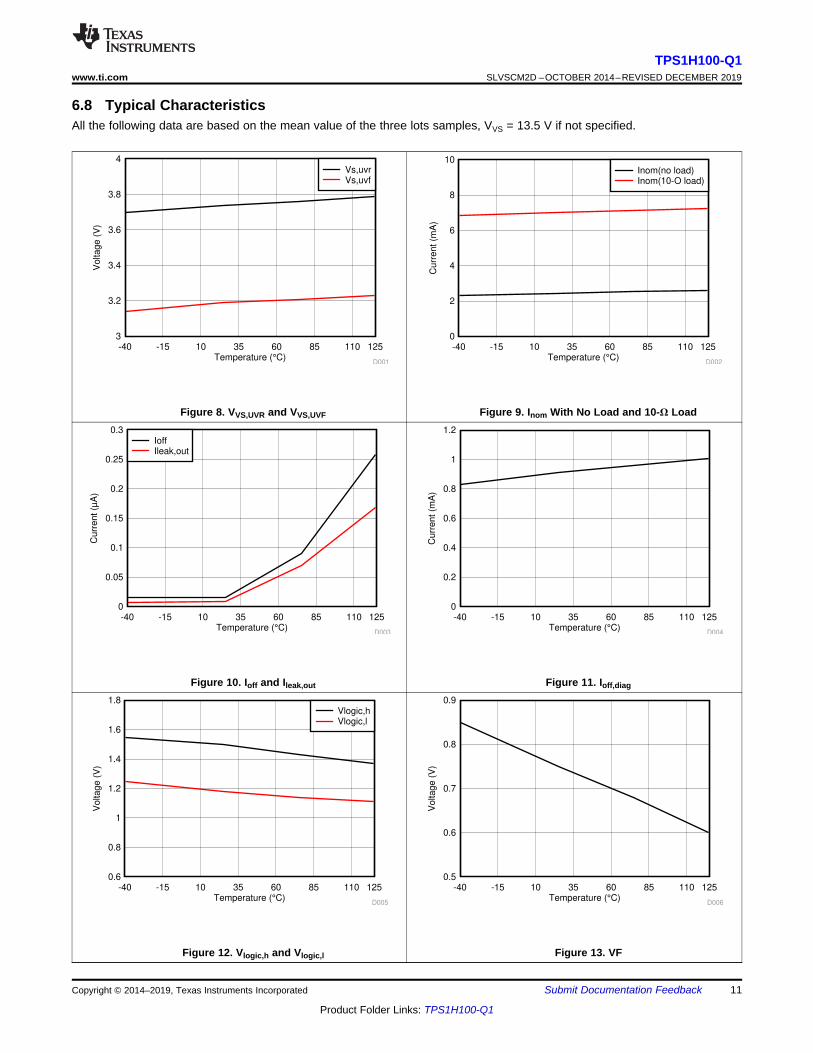
6.8 Typical CharacteristicsAll the following data are based on the mean value of the three lots samples, VVS = 13.5 V if not specified.
Figure 8. VVS,UVR and VVS,UVF Figure 9. Inom With No Load and 10-Ω Load
Figure 10. Ioff and Ileak,out Figure 11. Ioff,diag
Figure 12. Vlogic,h and Vlogic,l Figure 13. VF

Temperature (°C)
Sle
w R
ate
(V
/µS
)
-40 -15 10 35 60 85 110 1250.3
0.32
0.34
0.36
0.38
0.4
D011
dV/dtONdV/dtOFF
Temperature (°C)
Voltage (
V)
-40 -15 10 35 60 85 110 1254.3
4.4
4.5
4.6
4.7
4.8
4.9
5
D012
Temperature (°C)
Curr
ent (A
)
-40 -15 10 35 60 85 110 1259
9.5
10
10.5
11
D009Temperature (°C)
Tim
e (
µs)
-40 -15 10 35 60 85 110 12520
25
30
35
40
45
D010
TD_OnTD_Off
Temperature (°C)
Volta
ge
(V
)
-40 -15 10 35 60 85 110 12550
55
60
65
D007Temperature (°C)
Resis
tance (
mO
)
-40 -15 10 35 60 85 110 12555
70
85
100
115
130
D008
Rdson_VS_3P5VRdson_VS_5VRdson_VS_13P5Rdson_VS_40V
12
TPS1H100-Q1SLVSCM2D –OCTOBER 2014–REVISED DECEMBER 2019 www.ti.com
Product Folder Links: TPS1H100-Q1
Submit Documentation Feedback Copyright © 2014–2019, Texas Instruments Incorporated
Typical Characteristics (continued)All the following data are based on the mean value of the three lots samples, VVS = 13.5 V if not specified.
Figure 14. VDS, clamp Figure 15. RDSON
Figure 16. Ilim,nom Figure 17. TDon and TDoff
Figure 18. dV/dtON and dV/dtOFF Figure 19. VCS,h

Temperature (°C)-40 -10 20 50 80 110 125
-10%
-8%
-6%
-4%
-2%
0
2%
4%
6%
8%
10%
D019Temperature (°C)
-40 -10 20 50 80 110 125-10%
-8%
-6%
-4%
-2%
0
2%
4%
6%
8%
10%
D016
Temperature (°C)-40 -10 20 50 80 110 125
-20%
-15%
-10%
-5%
0
5%
10%
15%
20%
D015Temperature (°C)
-40 -10 20 50 80 110 125-10%
-8%
-6%
-4%
-2%
0
2%
4%
6%
8%
10%
D017
Temperature (°C)
Voltage (
V)
-40 -15 10 35 60 85 110 1251.7
1.75
1.8
1.85
1.9
1.95
D013Temperature (°C)
Curr
ent
(mA
)
-40 -15 10 35 60 85 110 1255
6
7
8
9
D014
13
TPS1H100-Q1www.ti.com SLVSCM2D –OCTOBER 2014–REVISED DECEMBER 2019
Product Folder Links: TPS1H100-Q1
Submit Documentation FeedbackCopyright © 2014–2019, Texas Instruments Incorporated
Typical Characteristics (continued)All the following data are based on the mean value of the three lots samples, VVS = 13.5 V if not specified.
Figure 20. Vol,off Figure 21. Iol,on
Figure 22. KCS = 5 mA, 13.5 V Figure 23. KCS = 25 mA, 13.5 V
Figure 24. KCS = 50 mA, 13.5 V Figure 25. KCS = 100 mA, 13.5 V

Temperature (°C)-40 -10 20 50 80 110 125
-10%
-8%
-6%
-4%
-2%
0
2%
4%
6%
8%
10%
D021
Temperature (°C)-40 -10 20 50 80 110 125
-10%
-8%
-6%
-4%
-2%
0
2%
4%
6%
8%
10%
D018Temperature (°C)
-40 -10 20 50 80 110 125-10%
-8%
-6%
-4%
-2%
0
2%
4%
6%
8%
10%
D020
14
TPS1H100-Q1SLVSCM2D –OCTOBER 2014–REVISED DECEMBER 2019 www.ti.com
Product Folder Links: TPS1H100-Q1
Submit Documentation Feedback Copyright © 2014–2019, Texas Instruments Incorporated
Typical Characteristics (continued)All the following data are based on the mean value of the three lots samples, VVS = 13.5 V if not specified.
Figure 26. KCS = 1 A, 13.5 V Figure 27. KCL = 0.5 A, 13.5 V
Figure 28. KCL = 1.6 A, 13.5 V

15
TPS1H100-Q1www.ti.com SLVSCM2D –OCTOBER 2014–REVISED DECEMBER 2019
Product Folder Links: TPS1H100-Q1
Submit Documentation FeedbackCopyright © 2014–2019, Texas Instruments Incorporated
7 Detailed Description
7.1 OverviewThe TPS1H100-Q1 is a single-channel, fully-protected, high-side power switch with an integrated NMOS powerFET and charge pump. Full diagnostics and high-accuracy current-sense features enable intelligent control of theload. A programmable current-limit function greatly improves the reliability of the whole system. The devicediagnostic reporting has two versions to support both digital status and analog current-sense output, both ofwhich can be set to the high-impedance state when diagnostics are disabled, for multiplexing the MCU analog ordigital interface among devices.
For version A, the digital status report is implemented with an open-drain structure. When a fault conditionoccurs, it pulls down to GND. A 3.3- or 5-V external pullup is required to match the microcontroller supply level.For version B, high-accuracy current sensing allows a better real-time monitoring effect and more-accuratediagnostics without further calibration. A current mirror is used to source 1 / K of the load current, which isreflected as voltage on the CS pin. K is a constant value across the temperature and supply voltage. The current-sensing function operates normally within a wide linear region from 0 to 4 V. The CS pin can also report a faultby pulling up the voltage of VCS,h.
The external high-accuracy current limit allows setting the current limit value by application. It highly improves thereliability of the system by clamping the inrush current effectively under start-up or short-circuit conditions. Also, itcan save system costs by reducing PCB trace, connector size, and the preceding power-stage capacity. Aninternal current limit is also implemented in this device. The lower value of the external or internal current-limitvalue is applied.
An active drain and source voltage clamp is built in to address switching off the energy of inductive loads, suchas relays, solenoids, pumps, motors, and so forth. During the inductive switching-off cycle, both the energy of thepower supply (EBAT) and the load (ELOAD) are dissipated on the high-side power switch itself. With the benefits ofprocess technology and excellent IC layout, the TPS1H100-Q1 device can achieve excellent power dissipationcapacity, which can help save the external free-wheeling circuitry in most cases. See Inductive-Load Switching-Off Clamp for more details.
Short-circuit reliability is critical for smart high-side power-switch devices. The standard of AEC-Q100-012 is todetermine the reliability of the devices when operating in a continuous short-circuit condition. Different gradelevels are specified according to the pass cycles. This device is qualified with the highest level, Grade A, 1million times short-to-GND certification.
The TPS1H100-Q1 device can be used as a high-side power switch for a wide variety of resistive, inductive, andcapacitive loads, including the low-wattage bulbs, LEDs, relays, solenoids, and heaters.

Gate Driver
Diagnostics
and Protection
Current Limit
IN
ST
CL
CS
SOURCE(OUT)
DRAIN (VS)
VDS Clamp
DIAG_EN
GND
Charge PumpInternal LDO
Internal
Reference
Current Sense
Open Load
Detection
Thermal
Monitor
16
TPS1H100-Q1SLVSCM2D –OCTOBER 2014–REVISED DECEMBER 2019 www.ti.com
Product Folder Links: TPS1H100-Q1
Submit Documentation Feedback Copyright © 2014–2019, Texas Instruments Incorporated
7.2 Functional Block Diagram
7.3 Feature Description
7.3.1 Accurate Current SenseFor version B, the high-accuracy current-sense function is internally implemented, which allows a better real-timemonitoring effect and more-accurate diagnostics without further calibration. A current mirror is used to source1 / K of the load current, flowing out to the external resistor between the CS pin and GND, and reflected asvoltage on the CS pin.
K is the ratio of the output current and the sense current. It is a constant value across the temperature andsupply voltage. Each device was internally calibrated while in production, so post-calibration by users is notrequired in most cases.

CS CSCS
CS out
V V KR
I I
u
5 mA
0 A
dK/K = ±80%
25 mA dK/K = ±10%
50 mA dK/K = ±7%
100 mA dK/K = ±5%
1 A dK/K = ±3%
4 A
17
TPS1H100-Q1www.ti.com SLVSCM2D –OCTOBER 2014–REVISED DECEMBER 2019
Product Folder Links: TPS1H100-Q1
Submit Documentation FeedbackCopyright © 2014–2019, Texas Instruments Incorporated
Feature Description (continued)
Figure 29. Current-Sense Accuracy
Ensure the CS voltage is in the linear region (0 to 4 V) during normal operation. Calculate RCS with Equation 1.
(1)
Also, when a fault condition occurs, CS works as a diagnostics report pin. When an open load or short to batteryoccurs in the on-state, VCS almost equals 0. When current limit, thermal shutdown/swing, open load, or short tobattery in the off-state occurs, the voltage is pulled up to VCS,h. Figure 30 shows a typical current-sense voltageaccording to the operating conditions, including fault conditions.

OUT
VS
VBAT
RCL
Iout/Kcl
Iout
Rcs
CLCS
Iout/K
CURRENT
CLAMP
Vcl,th
FAULT Vcs,H+
t
ADC Full Scale
Range
Max Normal
Operating Current
On-state: Current limit, thermal fault
Off-state: Open load/ short to battery Over
currentNormal
Open Load Current
On-state: open load/short to battery
Current Sense
Voltage
Operating
Range
Vcs,H
18
TPS1H100-Q1SLVSCM2D –OCTOBER 2014–REVISED DECEMBER 2019 www.ti.com
Product Folder Links: TPS1H100-Q1
Submit Documentation Feedback Copyright © 2014–2019, Texas Instruments Incorporated
Feature Description (continued)
Figure 30. Voltage Indication on the Current-Sense Pin
Figure 31. Current-Sense and Current-Limit Block Diagram
7.3.2 Programmable Current LimitA high-accuracy current limit allows higher reliability, which protects the power supply during short circuit orpower up. Also, it can save system costs by reducing PCB traces, connector size, and the capacity of thepreceding power stage.
Current limit offers protection from overstressing to the load and integrated power FET. Current limit holds thecurrent at the set value, and pulls up the CS pin to VCS,h as a diagnostic report. The two current-limit thresholdsare:• External programmable current limit -- An external resistor is used to convert a proportional load current into a
voltage, which is compared with an internal reference voltage, Vth,cl. When the voltage on the CL pin exceedsVth.cl, a closed loop steps in immediately. VGS voltage regulates accordingly, leading to the Vds voltageregulation. When the closed loop is set up, the current is clamped at the set value. The externalprogrammable current limit provides the capability to set the current-limit value by application.

2 BAT OUTHSD OUT(MAX) 2
V V1E L I
2 R
u u
BAT OUT OUT(MAX) OUTOUT(MAX) OUTHSD 2
OUT
V V R I V( / 5 , ± 9 OQ
VR
ª º § ·u « » u u u ¨ ¸¨ ¸« »© ¹¬ ¼
OUT(MAX) OUTDECAY
OUT
R I VLT ln
R V
§ ·u ¨ ¸ u¨ ¸© ¹
DECAYT
HSD DS,clamp OUT0
E V I (t)dt u³
HSD BAT LOAD BAT L R( ( ( ( ( ±(
DS,clamp BAT OUT9 9 ± 9
CL,th CL,th CLoutCL CL
CL CL out
V V KII R
R K I
u o
19
TPS1H100-Q1www.ti.com SLVSCM2D –OCTOBER 2014–REVISED DECEMBER 2019
Product Folder Links: TPS1H100-Q1
Submit Documentation FeedbackCopyright © 2014–2019, Texas Instruments Incorporated
Feature Description (continued)• Internal current limit -- The internal current limit is fixed and typically 10 A. To use the internal current limit for
large-current applications, tie the CL pin directly to the device GND.
Both the internal current limit (Ilim,nom) and external programmable current limit are always active when VVS ispowered and IN is high. The lower one (of Ilim,nom and the external programmable current limit) is applied as theactual current limit.
Note that if a GND network is used (which leads to the level shift between the device GND and board GND), theCL pin must be connected with device GND. Calculate RCL with Equation 2.
(2)
For better protection from a hard short-to-GND condition (when VS and input are high and a short to GNDhappens suddenly), an open-loop fast-response behavior is set to turn off the channel, before the current-limitclosed loop is set up. The open-loop response time is around 1 µs. With this fast response, the device canachieve better inrush-suppression performance.
7.3.3 Inductive-Load Switching-Off ClampWhen an inductive load is switching off, the output voltage is pulled down to negative, due to the inductancecharacteristics. The power FET may break down if the voltage is not clamped during the current-decay period. Toprotect the power FET in this situation, internally clamp the drain-to-source voltage, namely VDS,clamp, the clampdiode between the drain and gate.
(3)
During the current-decay period (TDECAY), the power FET is turned on for inductance-energy dissipation. Both theenergy of the power supply (EBAT) and the load (ELOAD) are dissipated on the high-side power switch itself, whichis called EHSD. If resistance is in series with inductance, some of the load energy is dissipated in the resistance.
(4)
From the high-side power switch’s view, EHSD equals the integration value during the current-decay period.
(5)
(6)
(7)
When R approximately equals 0, EHSD can be given simply as:
(8)

INPUT
VOUT
VBAT
IOUT
VDS, clamp
tDECAY
EHSD
R
VBAT
+
-
IN
SOURCE
DRAIN
GND
-L
20
TPS1H100-Q1SLVSCM2D –OCTOBER 2014–REVISED DECEMBER 2019 www.ti.com
Product Folder Links: TPS1H100-Q1
Submit Documentation Feedback Copyright © 2014–2019, Texas Instruments Incorporated
Feature Description (continued)
Figure 32. Driving Inductive Load
Figure 33. Inductive-Load Switching-Off Diagram
As discussed previously, when switching off, battery energy and load energy are dissipated on the high-sidepower switch, which leads to the large thermal variation. For each high-side power switch, the upper limit of themaximum safe power dissipation depends on the device intrinsic capacity, ambient temperature, and boarddissipation condition. TI provides the upper limit of single-pulse energy that devices can tolerate under the testcondition: VVS = 13.5 V, inductance from 0.1 mH to 400 mH, R = 0 Ω, FR4 2s2p board, 2- × 70-μm copper, 2- ×35-μm copper, thermal pad copper area 600 mm2.
For one dedicated inductance, see Figure 34. If the maximum switching-off current is lower than the currentvalue shown on the curve, the internal clamp function can be used for the demagnetization energy dissipation. Ifnot, external free-wheeling circuitry is necessary for device protection.

Inductance Range (mH)
Maxim
um
Curr
en
t (A
)
0.1 0.2 0.5 1 2 3 4 5 7 10 20 30 50 100 200 4004000
1
2
3
4
5
6
7
8
9
10
11
12
D026
TA = 25°CTA = 125°C
21
TPS1H100-Q1www.ti.com SLVSCM2D –OCTOBER 2014–REVISED DECEMBER 2019
Product Folder Links: TPS1H100-Q1
Submit Documentation FeedbackCopyright © 2014–2019, Texas Instruments Incorporated
Feature Description (continued)
(1) Need external pullup resistor during off-state
Figure 34. Maximum Current vs Inductance Range
7.3.4 Full Protections and DiagnosticsTable 1 is when DIAG_EN enabled. When DIAG_EN is low, current sense or ST is disabled accordingly. Theoutput is in high-impedance mode. Refer to Table 2 for details.
Table 1. Fault Table
CONDITIONS IN OUT CRITERION ST(Version A)
CS(Version B) Diagnostics Recovery
NormalL L H 0H H H In linear region
Short to GND H L Current limit triggered. L VCS,h AUTO
Open load (1)
Short to batteryReverse polarity
H H Version A: Output current < Iol,onVersion B: Judged by users L (deglitch) Almost 0 AUTO
L H VVS – VOUT < Vol,off L (deglitch) VCS,h (deglitch) AUTO
Thermal shutdown H TSD triggered L VCS,hRecovery whentemp < TSD,rst
Thermal swing H Tsw triggered L VCS,h AUTO
Table 2. DIAG_EN Logic TableDIAG_EN IN Condition Protections and Diagnostics
HIGHON See Table 1OFF See Table 1
LOWON Diagnostics disabled, protection normal
CS or ST is high Impedance
OFF Diagnostics disabled, no protectionsCS or ST is high impedance

OUT
VS
Vol,off
FAULT
OPEN LOAD
VBAT
ST/CS Rpu
Normal Operation
Region
18 mA
2 mA
80% Tolerance
25 mA10% Tolerance
22.5 mA
27.5 mA
10 mA
On State, Open Load/
Short to Battery
22
TPS1H100-Q1SLVSCM2D –OCTOBER 2014–REVISED DECEMBER 2019 www.ti.com
Product Folder Links: TPS1H100-Q1
Submit Documentation Feedback Copyright © 2014–2019, Texas Instruments Incorporated
7.3.4.1 Short-to-GND and Overload DetectionIn the on state, the short-to-GND fault is reported as the low status output or VCS,h on CS, when a current limit istriggered. The lower one of the internal and external set values is applied for the actual current limit. It is in auto-recovery when the fault condition is cleared. If not cleared, thermal shutdown triggers to protect the power FET.
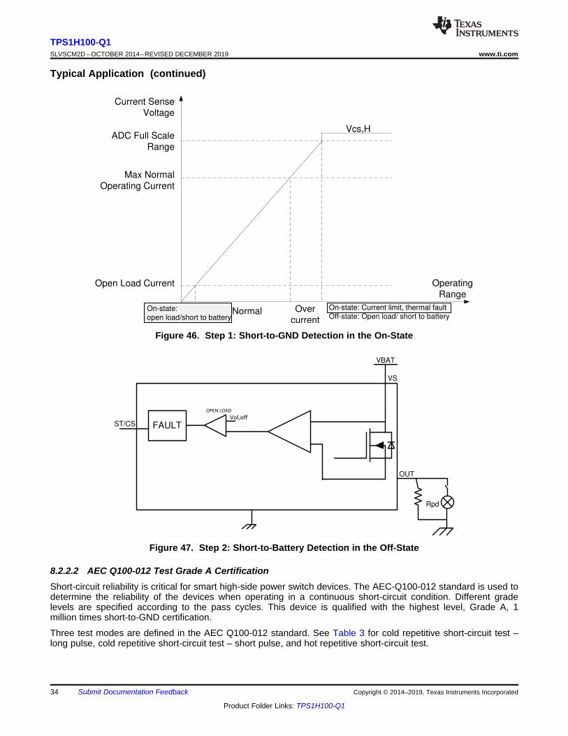
7.3.4.2 Open-Load DetectionIn the on state for version A, if the current flowing through the output is less than Iol,on, the device recognizes anopen-load fault. For version B, faults are diagnosed by reading the voltage on the CS pin and judged by the user.A benefit of high-accuracy current sense down to a verylow current range, this device can achieve a very lowopen-load detection threshold, which correspondingly expands the normal operation region. TI suggests 10 mAas the upper limit for the open-load detection threshold and 25 mA as the lower limit for the normal operationcurrent. In Figure 35, the recommended open-load detection region is shown as the dark-shaded region and thelight-shaded region is for normal operation. As a guideline, do not overlap these two regions.
Figure 35. On-State Open-Load Detection and Normal-Operation Diagram
In the off state, if a load is connected, the output voltage is pulled to 0 V. In the case of an open load, the outputvoltage is close to the supply voltage, VS – VOUT < Vol,off. For version A, the ST pin goes low to indicate the faultto the MCU. For version B, the CS pin is pulled up to VCS,h. There is always a leakage current Iol,off present onthe output, due to the internal logic control path or external humidity, corrosion, and so forth. Thus, TIrecommends an external pullup resistor to offset the leakage current. This pullup current should be less than theoutput load current to avoid false detection in the normal operation mode. To reduce the standby current, TIrecommends always to use a switch in series with? the pullup resistor. TI recommends Rpu ≤ 15 kΩ.
Figure 36. Open-Load Detection Circuit
23
TPS1H100-Q1www.ti.com SLVSCM2D –OCTOBER 2014–REVISED DECEMBER 2019
Product Folder Links: TPS1H100-Q1
Submit Documentation FeedbackCopyright © 2014–2019, Texas Instruments Incorporated
7.3.4.3 Short-to-Battery DetectionShort-to-battery detectioin has the same detection mechanism and behavior as open-load detection, both in theon-state and off-state. See the fault truth table, Table 1, for more details. In the on-state, the reverse currentflows through the FET instead of the body diode, leading to less power dissipation. Thus, the worst case for off-state is when reverse current occurs. In the off-state, if VOUT – VVS < VF, short to battery can be detected. (VF isthe body diode forward voltage and typically 0.7 V.) However, the reverse current does not occur. If VOUT – VVS >VF, short to battery can be detected, and the reverse current should be lower than Irev2 to ensure the survival ofthe device. TI recommends switching on the input for lower power dissipation or the reverse block circuitry for thesupply. See Reverse Current Protection for more external protection circuitry information.
7.3.4.4 Reverse-Polarity DetectionReverse-polarity detection has the same detection mechanism and behavior as open-load detection, both in theon-state and off-state. See the fault truth table, Table 1, for more details. In the on-state, the reverse currentflows through the FET instead of the body diode, leading to less power dissipation. Thus, the worst case off-stateis when reverse current occurs. In off-state, the reverse current should be lower than Irev1 to ensure the survivalof the device. See Reverse Current Protection for more external protection circuitry information.
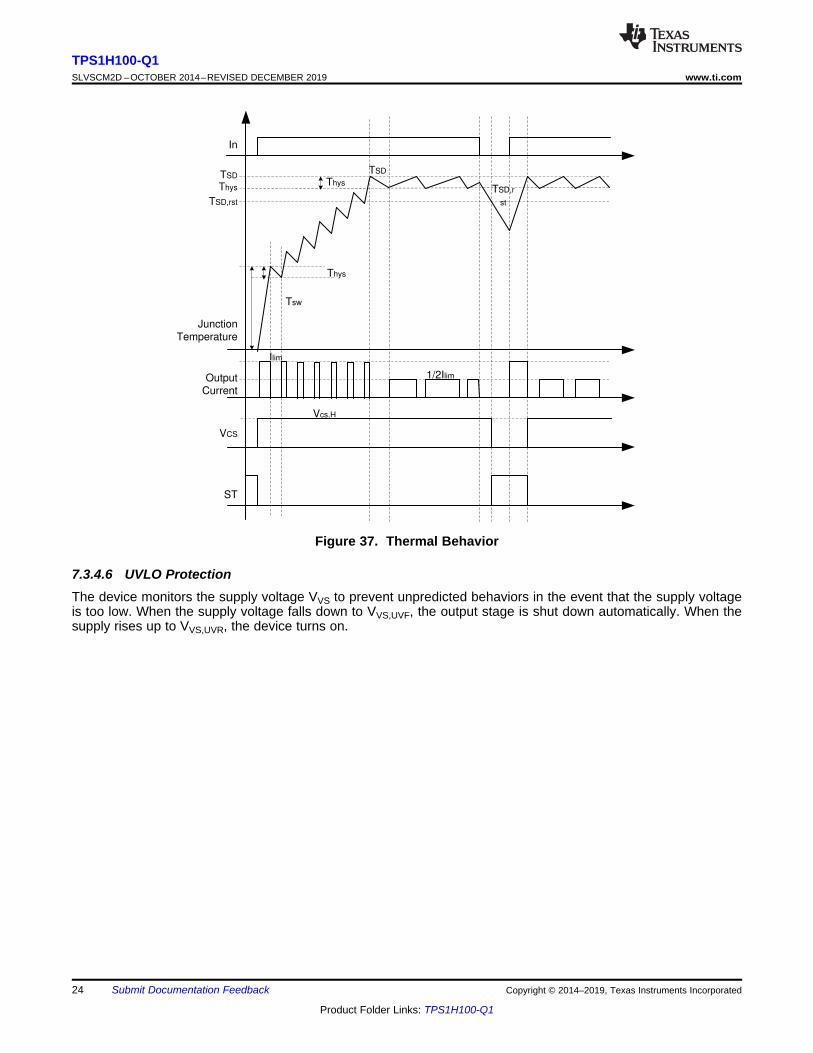
7.3.4.5 Thermal Protection BehaviorBoth the absolute temperature thermal shutdown and the dynamic temperature thermal swing diagnostic andprotection are built into the device to increase the maximum reliability of the power FET. Thermal swing is activewhen the temperature of the power FET is increasing sharply, that is ΔT = TDMOS – TLogic > Tsw, then the output isshut down, and the ST pin goes low, or the CS pin is pulled up to VCS,h. It auto-recovers and clears the faultsignal until ΔT = TDMOS – TLogic < Tsw – Thys. Thermal swing function improves device reliability against repetitivefast thermal variation, as shown in Figure 37. Multiple thermal swings are triggered before thermal shutdownhappens. Thermal shutdown is active when absolute temperature T > TSD. When active, the output is shut down,and the ST pin goes low, or the CS pin is pulled up to VCS,h. The output is auto-recovered when T < TSD – Thys;the current limit is reduced to Ilim,tsd, or half of the programmable current limit value, to avoid repeated thermalshutdown. However, the thermal shutdown fault signal and half-current limit value are not cleared until thejunction temperature decreases to less than TSD,rst.
Output
Current
VCS
ST
Junction
Temperature
TSD
In
Thys
Thys
Tsw
TSD,r
st
Thys
TSD
TSD,rst
Vcs,H
Ilim
1/2Ilim
24
TPS1H100-Q1SLVSCM2D –OCTOBER 2014–REVISED DECEMBER 2019 www.ti.com
Product Folder Links: TPS1H100-Q1
Submit Documentation Feedback Copyright © 2014–2019, Texas Instruments Incorporated
Figure 37. Thermal Behavior
7.3.4.6 UVLO ProtectionThe device monitors the supply voltage VVS to prevent unpredicted behaviors in the event that the supply voltageis too low. When the supply voltage falls down to VVS,UVF, the output stage is shut down automatically. When thesupply rises up to VVS,UVR, the device turns on.

IN
CL
CS
Version B
SOURCE
DRAIN
DIAG_EN
GND
NC
(Floating)
Load
ST
Version A
MCU
VBAT
5V
Tab
25
TPS1H100-Q1www.ti.com SLVSCM2D –OCTOBER 2014–REVISED DECEMBER 2019
Product Folder Links: TPS1H100-Q1
Submit Documentation FeedbackCopyright © 2014–2019, Texas Instruments Incorporated
7.3.4.7 Loss of GND ProtectionWhen loss of GND occurs, output is turned off regardless of whether the input signal is high or low.
Case 1 (loss of device GND): Loss of GND protection is active when the Tab, IC_GND, and current limit GND areone trace connected to the board GND, as shown in Figure 38. Tab floating is also a choice.
Figure 38. Loss of Device GND

IN
CL
CS
Version B
SOURCE
DRAIN
DIAG_EN
GND
NC
(Floating)
Load
ST
Version A
MCU
VBAT
5V
Tab
26
TPS1H100-Q1SLVSCM2D –OCTOBER 2014–REVISED DECEMBER 2019 www.ti.com
Product Folder Links: TPS1H100-Q1
Submit Documentation Feedback Copyright © 2014–2019, Texas Instruments Incorporated
Case 2 (loss of module GND): When the whole ECU module GND is lost, protections are also active. At thiscondition, the load GND remains connected.
Figure 39. Loss of Module GND

IN
CL
CS
SOURCE
DRAIN
DIAG_EN
GND
DgndRgnd
NC
(Floating)
ST
VBAT
L
D
Z
MCU
5V
27
TPS1H100-Q1www.ti.com SLVSCM2D –OCTOBER 2014–REVISED DECEMBER 2019
Product Folder Links: TPS1H100-Q1
Submit Documentation FeedbackCopyright © 2014–2019, Texas Instruments Incorporated
7.3.4.8 Loss of Power Supply ProtectionWhen loss of supply occurs, output is turned off regardless of whether the input is high or low. For a resistive orcapacitive load, loss-o-supply protection is easy to achieve due to no more power. The worst case is a chargedinductive load. In this case, the current is driven from all of the IOs to maintain the inductance output loop. TIrecommends either the MCU serial resistor plus the GND network (diode and resistor in parallel) or external free-wheeling circuitry.
Figure 40. Loss of Battery
Gate drive
and Clamp
Logic and
Protection
Current Sense/
Current Limit
IN
CURRENT LIMIT
CS
Version B
SOURCE
DRAINOutput
Clamp
DIAG_EN
GND
NC
(Floating)
Load
STATUS
Version A
VBAT
28
TPS1H100-Q1SLVSCM2D –OCTOBER 2014–REVISED DECEMBER 2019 www.ti.com
Product Folder Links: TPS1H100-Q1
Submit Documentation Feedback Copyright © 2014–2019, Texas Instruments Incorporated
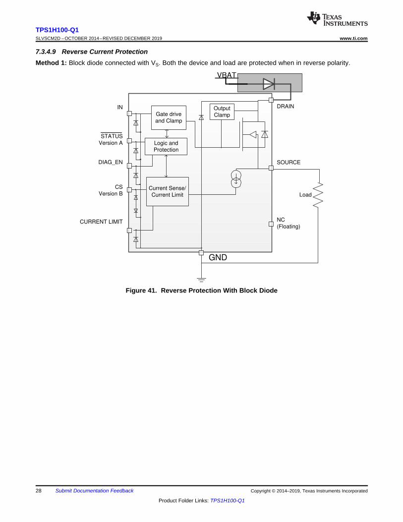
7.3.4.9 Reverse Current ProtectionMethod 1: Block diode connected with VS. Both the device and load are protected when in reverse polarity.
Figure 41. Reverse Protection With Block Diode

CC
GND
GND
±9R
±,t
GNDshiftGND
nom
VR
Id
Gate drive
and Clamp
Logic and
Protection
Current Sense/
Current Limit
IN
CURRENT LIMIT
CS
Version B
SOURCE
DRAINOutput
Clamp
DIAG_EN
GND
DgndRgnd
NC
(Floating)
Load
STATUS
Version A
VBAT
GND
Network
29
TPS1H100-Q1www.ti.com SLVSCM2D –OCTOBER 2014–REVISED DECEMBER 2019
Product Folder Links: TPS1H100-Q1
Submit Documentation FeedbackCopyright © 2014–2019, Texas Instruments Incorporated
Method 2 (GND network protection): Only the high-side device is protected under this connection. The loadreverse loop is limited by the load itself. Note when reverse polarity happens, the continuous reverse currentthrough the power FET should be less than Irev. Of the three types of ground pin networks, TI stronglyrecommends type 3 (the resistor and diode in parallel). No matter what types of connection are between thedevice GND and the board GND, if a GND voltage shift happens, ensure the following proper connections for thenormal operation:• Leave the NC pin floating or connect to the device GND. TI recommends to leave floating.• Connect the current limit programmable resistor to the device GND.
Figure 42. Reverse Protection With GND Network
• Type 1 (resistor): The higher resistor value contributes to a better current limit effect when the reversebattery or negative ISO pulses. However, it leads to higher GND shift during normal operation mode. Also,consider the resistor’s power dissipation.
(9)
where• VGNDshift is the maximum value for the GND shift, determined by the HSD and microcontroller. TI suggests a
value ≤ 0.6 V.• Inom is the nominal operating current.• –VCC is the maximum reverse voltage seen on the battery line.• –IGND is the maximum reverse current the ground pin can withstand, which is available in the Absolute
Maximum Ratings. (10)If multiple high-side power switches are used, the resistor can be shared among devices.
• Type 2 (diode): A diode is needed to block the reverse voltage, which also brings a ground shift (≈ 600 mV).

Gate drive
and Clamp
Logic and
Protection
Current Sense/
Current Limit
IN
CURRENT
LIMIT
CS
Version B
SOURCE
DRAINOutput
Clamp
DIAG_EN
GND
DgndRgnd
NC
(Floating)
Load
STATUS
Version A
MCU
VBAT
5V
30
TPS1H100-Q1SLVSCM2D –OCTOBER 2014–REVISED DECEMBER 2019 www.ti.com
Product Folder Links: TPS1H100-Q1
Submit Documentation Feedback Copyright © 2014–2019, Texas Instruments Incorporated
However, an inductive load is not acceptable to avoid an abnormal status when switching off.• Type 3 (resistor and diode in parallel (recommended)): A peak negative spike may occur when the
inductive load is switching off, which may damage the HSD or the diode. So, TI recommends a resistor inparallel with the diode when driving an inductive load. The recommended selection are 1-kΩ resistor inparallel with an IF > 100-mA diode. If multiple high-side switches are used, the resistor and diode can beshared among devices.
7.3.4.10 Protection for MCU I/OsIn many conditions, such as the negative ISO pulse, or the loss of battery with an inductive load, a negativepotential on the device GND pin may damage the MCU I/O pins [more likely, the internal circuitry connected tothe pins]. Therefore, the serial resistors between MCU and HSD are required.
Also, for proper protection against loss of GND, TI recommends 4.7 kΩ when using 3.3-V MCU I/Os; 10 kΩ is for5-V applications.
Figure 43. MCU IO Protections
7.3.5 Diagnostic Enable FunctionThe diagnostic enable pin, DIAG_EN, offers multiplexing of the microcontroller diagnostic input for current senseor digital status, by sharing the same sense resistor and ADC line or I/O port among multiple devices.

DIAG_EN low and
IN high to low and
t > toff,deg
DIAG_EN
high to low
DIAG_EN
low to high
IN low to high
IN high to low and
DIAG_EN high and
t > toff,deg
IN low to high
Standby Mode
(IN low, DIAG low)
Standby mode
with diagnostic
(IN low, DIAG high)
Normal Mode
(IN high)
31
TPS1H100-Q1www.ti.com SLVSCM2D –OCTOBER 2014–REVISED DECEMBER 2019
Product Folder Links: TPS1H100-Q1
Submit Documentation FeedbackCopyright © 2014–2019, Texas Instruments Incorporated
In addition, during the output-off period, the diagnostic disable function lowers the current consumption for thestandby condition. The three working modes in the device are normal mode, standby mode, and standby modewith diagnostic. If off-state power saving is required in the system, the standby current is <500 nA with DIAG_ENlow. If the off-state diagnostic is required in the system, the typical standby current is around 1 mA withDIAG_EN high.
7.4 Device Functional Modes
7.4.1 Working ModeThe three working modes in the device are normal mode, standby mode, and standby mode with diagnostic. If anoff-state power saving is required in the system, the standby current is less than 500 nA with DIAG_EN low. If anoff-state diagnostic is required in the system, the typical standby current is around 1 mA with DIAG_EN high.Note that to enter standby mode requires IN low and t > toff,deg. toff,deg is the standby-mode deglitch time, which isused to avoid false triggering. Figure 44 shows a work-mode state-machine state diagram.
Figure 44. Work-Mode State Machine

Gate drive
and Clamp
Logic and
Protection
Current Sense/
Current Limit
IN
CL
CS
Version B
SOURCE
DRAINOutput
Clamp
DIAG_EN
GND
DgndRgnd
NC
(Floating)
Load
ST
Version A
MCU
VBAT
5V
RCS
RCL
RSER
GND Network
32
TPS1H100-Q1SLVSCM2D –OCTOBER 2014–REVISED DECEMBER 2019 www.ti.com
Product Folder Links: TPS1H100-Q1
Submit Documentation Feedback Copyright © 2014–2019, Texas Instruments Incorporated
8 Application and Implementation
NOTEInformation in the following applications sections is not part of the TI componentspecification, and TI does not warrant its accuracy or completeness. TI’s customers areresponsible for determining suitability of components for their purposes. Customers shouldvalidate and test their design implementation to confirm system functionality.
8.1 Application InformationThe following discussion notes how to implement the device to distinguish the different fault modes andimplement a ? transient-pulse immunity test.
In some applications, open load, short to battery, and short to GND must be distinguished from each other. Thisrequires two steps.
8.2 Typical ApplicationFigure 45 shows an example of how to design the external circuitry parameters.
Figure 45. Typical Application Circuitry

cl,th CLCL
OUT
V K 1.233 2000R 493.2
I 5
u u :
CS CSCS
CS OUT
V V K 3 500R 750
I I 2
u u :
33
TPS1H100-Q1www.ti.com SLVSCM2D –OCTOBER 2014–REVISED DECEMBER 2019
Product Folder Links: TPS1H100-Q1
Submit Documentation FeedbackCopyright © 2014–2019, Texas Instruments Incorporated
Typical Application (continued)8.2.1 Design Requirements• VS range from 9 V to 16 V• Nominal current of 2 A• Current sense for fault monitoring• Expected current limit value of 5 A• Full diagnostics with 5-V MCU• Reverse protection with GND network
8.2.2 Detailed Design ProcedureThe RCS, VCS linear region is from 0 to 4 V. To keep the 2-A nominal current in the 0- to 3-V range, calculate theRCS as in Equation 11. To achieve better current sense accuracy, a 1% accuracy or better resistor is preferred.
(11)
RCL, VCL,th is the current-limit internal threshold, 1.233 V. To set the programmable current limit value at 5 A,calculate the RCL as in Equation 12.
(12)
TI recommends RSER = 10 kΩ for 5-V MCU.
TI recommends a 1-kΩ resistor and 200-V, 0.2-A diode for the GND network.
8.2.2.1 Distinguishing of Different Fault ModesSome applications require that open load, short to battery, and short to GND can be distinguished from eachother. This requires two steps:1. In the on-state, for the current-sense version device (version B), on-state open load and short to battery are
recognized as an extremely-low voltage level on the current-sense pin, whereas short to GND is reported asa pulled-up voltage VCS,h. Therefore, the user can find a short to GND (see Figure 46).
2. If reported as an on-state open-load or short-to-battery fault in the first step, turn off the input signal. In theoff-state, with an external pulldown resistor, open load and short to battery can be easily distinguished. Whenthe output pulls down, the short to battery is still reported as an off-state fault condition, whereas the openload is ignored.
OUT
VS
Vol,off
FAULT
OPEN LOAD
VBAT
ST/CS
Rpd
ADC Full Scale
Range
Max Normal
Operating Current
On-state: Current limit, thermal fault
Off-state: Open load/ short to battery Over
currentNormal
Open Load Current
On-state:
open load/short to battery
Current Sense
Voltage
Operating
Range
Vcs,H
34
TPS1H100-Q1SLVSCM2D –OCTOBER 2014–REVISED DECEMBER 2019 www.ti.com
Product Folder Links: TPS1H100-Q1
Submit Documentation Feedback Copyright © 2014–2019, Texas Instruments Incorporated
Typical Application (continued)
Figure 46. Step 1: Short-to-GND Detection in the On-State
Figure 47. Step 2: Short-to-Battery Detection in the Off-State
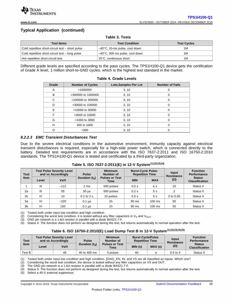
8.2.2.2 AEC Q100-012 Test Grade A CertificationShort-circuit reliability is critical for smart high-side power switch devices. The AEC-Q100-012 standard is used todetermine the reliability of the devices when operating in a continuous short-circuit condition. Different gradelevels are specified according to the pass cycles. This device is qualified with the highest level, Grade A, 1million times short-to-GND certification.
Three test modes are defined in the AEC Q100-012 standard. See Table 3 for cold repetitive short-circuit test –long pulse, cold repetitive short-circuit test – short pulse, and hot repetitive short-circuit test.
35
TPS1H100-Q1www.ti.com SLVSCM2D –OCTOBER 2014–REVISED DECEMBER 2019
Product Folder Links: TPS1H100-Q1
Submit Documentation FeedbackCopyright © 2014–2019, Texas Instruments Incorporated
Typical Application (continued)Table 3. Tests
Test Items Test Condition Test CyclesCold repetitive short-circuit test – short pulse –40°C, 10-ms pulse, cool down 1MCold repetitive short-circuit test – long pulse –40°C, 300-ms pulse, cool down 1MHot repetitive short-circuit test 25°C, continuous short 1M
Different grade levels are specified according to the pass cycles. The TPS1H100-Q1 device gets the certificationof Grade A level, 1 million short-to-GND cycles, which is the highest test standard in the market.
Table 4. Grade LevelsGrade Number of Cycles Lots,Samples Per Lot Number of Fails
A >1000000 3, 10 0B >300000 to 1000000 3, 10 0C >100000 to 300000 3, 10 0D >30000 to 100000 3, 10 0E >10000 to 30000 3, 10 0F >3000 to 10000 3, 10 0G >1000 to 3000 3, 10 0H 300 to 1000 3, 10 0O <300 3, 10 0
(1) Tested both under input low condition and high condition.(2) Considering the worst test condition, it is tested without any filter capacitors in VS and VOUT.(3) GND pin network is a 1-kΩ resistor in parallel with a diode BAS21-7-F.(4) Status II: The function does not perform as designed during the test, but returns automatically to normal operation after the test.
8.2.2.3 EMC Transient Disturbances TestDue to the severe electrical conditions in the automotive environment, immunity capacity against electricaltransient disturbances is required, especially for a high-side power switch, which is connected directly to thebattery. Detailed test requirements are in accordance with the ISO 7637-2:2011 and ISO 16750-2:2010standards. The TPS1H100-Q1 device is tested and certificated by a third-party organization.
Table 5. ISO 7637-2:2011(E) in 12-V System (1) (2) (3) (4)
TestItem
Test Pulse Severity Leveland vs Accordingly Pulse
Duration (td)
MinimumNumber of
Pulses or TestTime
Burst-Cycle Pulse-Repetition Time Input
Resistance(Ω)
FunctionPerformance
StatusClassificationLevel Vs/V MIN MAX
1 III –112 2 ms 500 pulses 0.5 s e s 10 Status II2a III 55 50 µs 500 pulses 0.2 s 5 s 2 Status II2b IV 10 0.2 to 2 s 10 pulses 0.5 s 5 s 0 to 0.05 Status II3a IV –220 0.1 µs 1h 90 ms 100 ms 50 Status II3b IV 150 0.1 µs 1h 90 ms 100 ms 50 Status II
(1) Tested both under input low condition and high condition. [DIAG_EN, IN, and VS are all classified as inputs. Which one?(2) Considering the worst test condition, the device is tested without any filter capacitors on VS and OUT.(3) The GND pin network is a 1-kΩ resistor in parallel with a diode BAS21-7-F.(4) Status II: The function does not perform as designed during the test, but returns automatically to normal operation after the test.(5) Select a 45-V external suppressor.
Table 6. ISO 16750-2:2010(E) Load Dump Test B in 12-V System (1) (2) (3) (4) (5)
TestItem
Test Pulse Severity Leveland vs Accordingly Pulse
Duration (td)
MinimumNumber of
Pulses or TestTime
Burst Cycle/PulseRepetition Time Input
Resistance(Ω)
FunctionPerformance
StatusClassificationLevel Vs/V MIN (s) MAX (s)
Test B 45 40 to 400 ms 5 pulses 60 e 0.5 to 4 Status II

Fast loop response
Closed loop response
1.8 A inrush
1 A inrush
2 A inrush
Input Step
36
TPS1H100-Q1SLVSCM2D –OCTOBER 2014–REVISED DECEMBER 2019 www.ti.com
Product Folder Links: TPS1H100-Q1
Submit Documentation Feedback Copyright © 2014–2019, Texas Instruments Incorporated
8.2.3 Application CurvesFigure 48 shows a test example of initial short-circuit inrush-current limit. Test conditions: VS = 13.5 V, input isfrom low to high, load is short-to-GND or with a 470-µF capacitive load, external current limit is 2 A. CH1 is theoutput current. CH3 is the input step.
Figure 49 shows a test example of a hard short-circuit inrush-current limit. Test conditions: VS= 13.5 V, input ishigh, load is 5 µH + 100 mΩ, external current limit is 1 A. A short to GND suddenly happens.
Figure 48. Initial Short-to-GND Waveform Figure 49. Hard Short-to-GND Waveform

VS
VS
VS
OUT
OUT
OUT
13
1
2
3
4
5
6
7 8
9
10
11
12
14
Thermal
Pad
GND
NC
IN
NC
NC
ST/CS
DIAG_EN
CL
37
TPS1H100-Q1www.ti.com SLVSCM2D –OCTOBER 2014–REVISED DECEMBER 2019
Product Folder Links: TPS1H100-Q1
Submit Documentation FeedbackCopyright © 2014–2019, Texas Instruments Incorporated
9 Power Supply RecommendationsThe device is qualified for both automotive and industrial applications. The normal power supply connection is a12-V automotive system or 24-V industrial system. The supply voltage should be within the range specified in theRecommended Operating Conditions.
10 Layout
10.1 Layout GuidelinesTo prevent thermal shutdown, TJ must be less than 150°C. If the output current is very high, the powerdissipation may be large. The HTSSOP package has good thermal impedance. However, the PCB layout is veryimportant. Good PCB design can optimize heat transfer, which is absolutely essential for the long-term reliabilityof the device.• Maximize the copper coverage on the PCB to increase the thermal conductivity of the board. The major heat-
flow path from the package to the ambient is through the copper on the PCB. Maximum copper is extremelyimportant when there are not any heat sinks attached to the PCB on the other side of the board opposite thepackage.
• Add as many thermal vias as possible directly under the package ground pad to optimize the thermalconductivity of the board.
• All thermal vias should either be plated shut or plugged and capped on both sides of the board to preventsolder voids. To ensure reliability and performance, the solder coverage should be at least 85%.
10.2 Layout Example
10.2.1 Without a GND NetworkWithout a GND network, tie the thermal pad directly to the board GND copper for better thermal performance.
Figure 50. Layout Without a GND Network

J A JA TT T R PT
u
2
T OUT DSON S nomP I R V I u u
VS
VS
VS
OUT
OUT
OUT
13
1
2
3
4
5
6
7 8
9
10
11
12
14
GND
NC
IN
NC
NC
ST/CS
DIAG_EN
CL
Thermal
Pad
GND Network
38
TPS1H100-Q1SLVSCM2D –OCTOBER 2014–REVISED DECEMBER 2019 www.ti.com
Product Folder Links: TPS1H100-Q1
Submit Documentation Feedback Copyright © 2014–2019, Texas Instruments Incorporated
Layout Example (continued)10.2.2 With a GND NetworkWith a GND network, tie the thermal pad with a single trace through the GND network to the board GND copper.
Figure 51. Layout With a GND Network
10.3 Thermal ConsiderationsThis device possesses thermal shutdown (TSD) circuitry as a protection from overheating. For continuous normaloperation, the junction temperature should not exceed the thermal-shutdown trip point. If the junction temperatureexceeds the thermal-shutdown trip point, the output turns off. When the junction temperature falls below thethermal-shutdown trip point, the output turns on again.
Calculate the power dissipated by the device according to Equation 13.
where• PT = Total power dissipation of the device (13)
After determining the power dissipated by the device, calculate the junction temperature from the ambienttemperature and the device thermal impedance.
(14)

39
TPS1H100-Q1www.ti.com SLVSCM2D –OCTOBER 2014–REVISED DECEMBER 2019
Product Folder Links: TPS1H100-Q1
Submit Documentation FeedbackCopyright © 2014–2019, Texas Instruments Incorporated
11 Device and Documentation Support
11.1 Receiving Notification of Documentation UpdatesTo receive notification of documentation updates, navigate to the device product folder on ti.com. In the upperright corner, click on Alert me to register and receive a weekly digest of any product information that haschanged. For change details, review the revision history included in any revised document.
11.2 Community ResourcesTI E2E™ support forums are an engineer's go-to source for fast, verified answers and design help — straightfrom the experts. Search existing answers or ask your own question to get the quick design help you need.
Linked content is provided "AS IS" by the respective contributors. They do not constitute TI specifications and donot necessarily reflect TI's views; see TI's Terms of Use.
11.3 TrademarksE2E is a trademark of Texas Instruments.All other trademarks are the property of their respective owners.
11.4 Electrostatic Discharge CautionThese devices have limited built-in ESD protection. The leads should be shorted together or the device placed in conductive foamduring storage or handling to prevent electrostatic damage to the MOS gates.
11.5 GlossarySLYZ022 — TI Glossary.
This glossary lists and explains terms, acronyms, and definitions.
12 Mechanical, Packaging, and Orderable InformationThe following pages include mechanical, packaging, and orderable information. This information is the mostcurrent data available for the designated devices. This data is subject to change without notice and revision ofthis document. For browser-based versions of this data sheet, refer to the left-hand navigation.
PACKAGE OPTION ADDENDUM
www.ti.com 10-Dec-2020
Addendum-Page 1
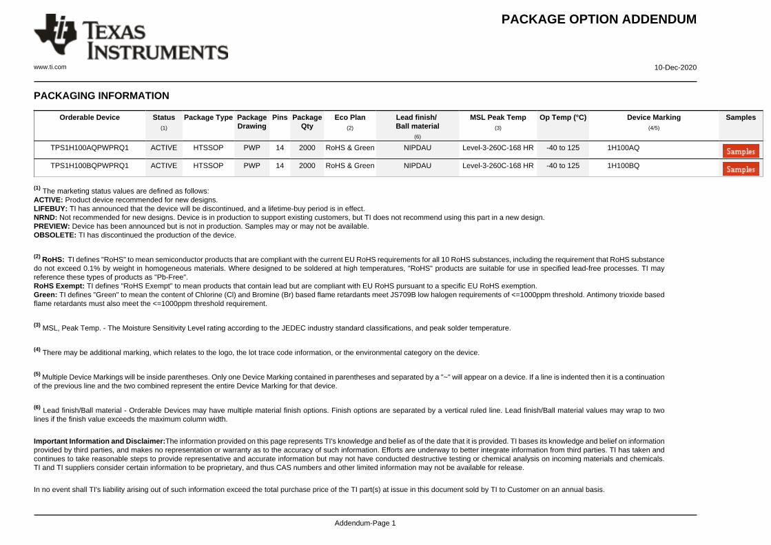
PACKAGING INFORMATION
Orderable Device Status(1)
Package Type PackageDrawing
Pins PackageQty
Eco Plan(2)
Lead finish/Ball material
(6)
MSL Peak Temp(3)
Op Temp (°C) Device Marking(4/5)
Samples
TPS1H100AQPWPRQ1 ACTIVE HTSSOP PWP 14 2000 RoHS & Green NIPDAU Level-3-260C-168 HR -40 to 125 1H100AQ
TPS1H100BQPWPRQ1 ACTIVE HTSSOP PWP 14 2000 RoHS & Green NIPDAU Level-3-260C-168 HR -40 to 125 1H100BQ
(1) The marketing status values are defined as follows:ACTIVE: Product device recommended for new designs.LIFEBUY: TI has announced that the device will be discontinued, and a lifetime-buy period is in effect.NRND: Not recommended for new designs. Device is in production to support existing customers, but TI does not recommend using this part in a new design.PREVIEW: Device has been announced but is not in production. Samples may or may not be available.OBSOLETE: TI has discontinued the production of the device.
(2) RoHS: TI defines "RoHS" to mean semiconductor products that are compliant with the current EU RoHS requirements for all 10 RoHS substances, including the requirement that RoHS substancedo not exceed 0.1% by weight in homogeneous materials. Where designed to be soldered at high temperatures, "RoHS" products are suitable for use in specified lead-free processes. TI mayreference these types of products as "Pb-Free".RoHS Exempt: TI defines "RoHS Exempt" to mean products that contain lead but are compliant with EU RoHS pursuant to a specific EU RoHS exemption.Green: TI defines "Green" to mean the content of Chlorine (Cl) and Bromine (Br) based flame retardants meet JS709B low halogen requirements of <=1000ppm threshold. Antimony trioxide basedflame retardants must also meet the <=1000ppm threshold requirement.
(3) MSL, Peak Temp. - The Moisture Sensitivity Level rating according to the JEDEC industry standard classifications, and peak solder temperature.
(4) There may be additional marking, which relates to the logo, the lot trace code information, or the environmental category on the device.
(5) Multiple Device Markings will be inside parentheses. Only one Device Marking contained in parentheses and separated by a "~" will appear on a device. If a line is indented then it is a continuationof the previous line and the two combined represent the entire Device Marking for that device.
(6) Lead finish/Ball material - Orderable Devices may have multiple material finish options. Finish options are separated by a vertical ruled line. Lead finish/Ball material values may wrap to twolines if the finish value exceeds the maximum column width.
Important Information and Disclaimer:The information provided on this page represents TI's knowledge and belief as of the date that it is provided. TI bases its knowledge and belief on informationprovided by third parties, and makes no representation or warranty as to the accuracy of such information. Efforts are underway to better integrate information from third parties. TI has taken andcontinues to take reasonable steps to provide representative and accurate information but may not have conducted destructive testing or chemical analysis on incoming materials and chemicals.TI and TI suppliers consider certain information to be proprietary, and thus CAS numbers and other limited information may not be available for release.
In no event shall TI's liability arising out of such information exceed the total purchase price of the TI part(s) at issue in this document sold by TI to Customer on an annual basis.

PACKAGE OPTION ADDENDUM
www.ti.com 10-Dec-2020
Addendum-Page 2

TAPE AND REEL INFORMATION
*All dimensions are nominal
Device PackageType
PackageDrawing
Pins SPQ ReelDiameter
(mm)
ReelWidth
W1 (mm)
A0(mm)
B0(mm)
K0(mm)
P1(mm)
W(mm)
Pin1Quadrant
TPS1H100AQPWPRQ1 HTSSOP PWP 14 2000 330.0 12.4 6.9 5.6 1.6 8.0 12.0 Q1
TPS1H100BQPWPRQ1 HTSSOP PWP 14 2000 330.0 12.4 6.9 5.6 1.6 8.0 12.0 Q1
PACKAGE MATERIALS INFORMATION
www.ti.com 17-Dec-2019
Pack Materials-Page 1

*All dimensions are nominal
Device Package Type Package Drawing Pins SPQ Length (mm) Width (mm) Height (mm)
TPS1H100AQPWPRQ1 HTSSOP PWP 14 2000 350.0 350.0 43.0
TPS1H100BQPWPRQ1 HTSSOP PWP 14 2000 350.0 350.0 43.0
PACKAGE MATERIALS INFORMATION
www.ti.com 17-Dec-2019
Pack Materials-Page 2


IMPORTANT NOTICE AND DISCLAIMER
TI PROVIDES TECHNICAL AND RELIABILITY DATA (INCLUDING DATASHEETS), DESIGN RESOURCES (INCLUDING REFERENCE DESIGNS), APPLICATION OR OTHER DESIGN ADVICE, WEB TOOLS, SAFETY INFORMATION, AND OTHER RESOURCES “AS IS” AND WITH ALL FAULTS, AND DISCLAIMS ALL WARRANTIES, EXPRESS AND IMPLIED, INCLUDING WITHOUT LIMITATION ANY IMPLIED WARRANTIES OF MERCHANTABILITY, FITNESS FOR A PARTICULAR PURPOSE OR NON-INFRINGEMENT OF THIRD PARTY INTELLECTUAL PROPERTY RIGHTS.These resources are intended for skilled developers designing with TI products. You are solely responsible for (1) selecting the appropriate TI products for your application, (2) designing, validating and testing your application, and (3) ensuring your application meets applicable standards, and any other safety, security, or other requirements. These resources are subject to change without notice. TI grants you permission to use these resources only for development of an application that uses the TI products described in the resource. Other reproduction and display of these resources is prohibited. No license is granted to any other TI intellectual property right or to any third party intellectual property right. TI disclaims responsibility for, and you will fully indemnify TI and its representatives against, any claims, damages, costs, losses, and liabilities arising out of your use of these resources.TI’s products are provided subject to TI’s Terms of Sale (www.ti.com/legal/termsofsale.html) or other applicable terms available either on ti.com or provided in conjunction with such TI products. TI’s provision of these resources does not expand or otherwise alter TI’s applicable warranties or warranty disclaimers for TI products.
Mailing Address: Texas Instruments, Post Office Box 655303, Dallas, Texas 75265Copyright © 2020, Texas Instruments Incorporated