tps22810-q1, 2.7-18-v, 79-mΩ on-resistance … free-air temperature range of –40˚c to +105˚c....
TRANSCRIPT

PowerSupply
EN/UVLO
GND
VIN
CT
VOUT
OFF
ON
TPS22810
QOD
CL RLCIN
Product
Folder
Order
Now
Technical
Documents
Tools &
Software
Support &Community
An IMPORTANT NOTICE at the end of this data sheet addresses availability, warranty, changes, use in safety-critical applications,intellectual property matters and other important disclaimers. PRODUCTION DATA.
TPS22810-Q1SLVSEJ0 –APRIL 2018
TPS22810-Q1, 2.7-18-V, 79-mΩ On-Resistance Load Switch With Thermal Protection
1
1 Features1• Qualified for Automotive Applications• AEC-Q100 Qualified With the Following Results:
– Device Temperature Grade 2: –40°C to+105°CAmbient Operating Temperature
– Device HBM ESD Classification Level 2– Device CDM ESD Classification Level C5
• Integrated Single Channel Load Switch• 2-A Maximum Continuous Current• Input Voltage: 2.7 V to 18 V• Absolute Maximum Input Voltage: 20 V• On-Resistance (RON)
– RON = 79 mΩ (Typical) at VIN = 12 V• Quiescent Current
– 62 µA (Typical) at VIN = 12 V• Shutdown Current
– 500 nA (Typical) at VIN = 12 V• Thermal Shutdown• Undervoltage Lock-Out (UVLO)• Adjustable Quick Output Discharge (QOD)• Configurable Rise Time With CT Pin• SOT23-6 Package
– 2.9-mm × 2.8-mm, 0.95-mm Pitch,1.45-mm Height (DBV)
2 Applications• Automotive Head Unit• Surround View ECU
3 DescriptionThe TPS22810-Q1 is a one channel load switch withconfigurable rise time and integrated quick outputdischarge (QOD). The device features thermalshutdown to protect the device against high junctiontemperature and thereby ensure safe operating areaof the device inherently. The device features a N-channel MOSFET that can operate over an inputvoltage range of 2.7 V to 18 V. The device cansupport a maximum current of 2 A. The switch iscontrolled by an on and off input that can interfacedirectly with low-voltage control signals.
The configurable rise time of the device greatlyreduces inrush current caused by large bulk loadcapacitances, thereby reducing or eliminating powersupply droop. Undervoltage lock-out is used to turnoff the device if the VIN voltage drops below athreshold value, ensuring that the downstreamcircuitry is not damaged by being supplied by avoltage lower than intended. The configurable QODpin controls the fall time of the device to allow designflexibility for power down.
The TPS22810-Q1 is available in a leaded, SOT-23package (DBV) which allows to visually inspect solderjoints. The device is characterized for operation overthe free-air temperature range of –40˚C to +105˚C.
Device Information(1)
PART NUMBER PACKAGE BODY SIZE (NOM)TPS22810-Q1 SOT-23 (6) 2.90 mm × 2.80 mm
(1) For all available packages, see the orderable addendum atthe end of the data sheet.
Simplified Schematic

2
TPS22810-Q1SLVSEJ0 –APRIL 2018 www.ti.com
Product Folder Links: TPS22810-Q1
Submit Documentation Feedback Copyright © 2018, Texas Instruments Incorporated
Table of Contents1 Features .................................................................. 12 Applications ........................................................... 13 Description ............................................................. 14 Revision History..................................................... 25 Pin Configuration and Functions ......................... 36 Specifications......................................................... 4
6.1 Absolute Maximum Ratings ...................................... 46.2 ESD Ratings.............................................................. 46.3 Recommended Operating Conditions....................... 46.4 Thermal Information .................................................. 46.5 Electrical Characteristics........................................... 56.6 Switching Characteristics .......................................... 66.7 Typical DC Characteristics ....................................... 76.8 Typical AC Characteristics........................................ 8
7 Parameter Measurement Information ................ 108 Detailed Description ............................................ 11
8.1 Overview ................................................................. 118.2 Functional Block Diagram ....................................... 118.3 Feature Description................................................. 12
8.4 Device Functional Modes........................................ 159 Application and Implementation ........................ 16
9.1 Application Information............................................ 169.2 Typical Application ................................................. 16
10 Power Supply Recommendations ..................... 2111 Layout................................................................... 22
11.1 Layout Guidelines ................................................. 2211.2 Layout Example .................................................... 2211.3 Thermal Considerations ........................................ 22
12 Device and Documentation Support ................. 2312.1 Device Support...................................................... 2312.2 Documentation Support ........................................ 2312.3 Receiving Notification of Documentation Updates 2312.4 Community Resources.......................................... 2312.5 Trademarks ........................................................... 2312.6 Electrostatic Discharge Caution............................ 2312.7 Glossary ................................................................ 23
13 Mechanical, Packaging, and OrderableInformation ........................................................... 23
4 Revision History
DATE REVISION NOTESApril 2018 * Initial release.

VIN VOUT
CTEN/UVLO
GND QOD
1
2
3
6
5
4
3
TPS22810-Q1www.ti.com SLVSEJ0 –APRIL 2018
Product Folder Links: TPS22810-Q1
Submit Documentation FeedbackCopyright © 2018, Texas Instruments Incorporated
5 Pin Configuration and Functions
DBV Package6-Pin SOT-23
Top View
Pin FunctionsPIN
I/O DESCRIPTIONNAME NO.
CT 4 O Switch slew rate control. Can be left floatingEN/UVLO 3 I Active high switch control input and UVLO adjustment. Do not leave floatingGND 2 — Device ground
QOD 5 O
Quick Output Discharge pin. This functionality can be enabled in one of threeways:• Placing an external resistor between VOUT and QOD• Tying QOD directly to VOUT and using the internal resistor value (RPD)• Disabling QOD by leaving pin floatingSee the Quick Output Discharge (QOD) for more information
VIN 1 I Switch input. Place ceramic bypass capacitor(s) between this pin and GNDVOUT 6 O Switch output
4
TPS22810-Q1SLVSEJ0 –APRIL 2018 www.ti.com
Product Folder Links: TPS22810-Q1
Submit Documentation Feedback Copyright © 2018, Texas Instruments Incorporated
(1) Stresses beyond those listed under Absolute Maximum Rating may cause permanent damage to the device. These are stress ratingsonly, which do not imply functional operation of the device at these or any other conditions beyond those indicated under RecommendedOperating Condition. Exposure to absolute-maximum-rated conditions for extended periods may affect device reliability.
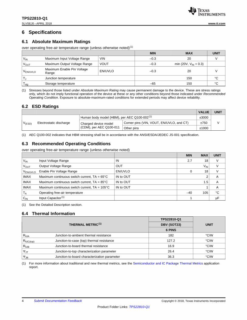
6 Specifications
6.1 Absolute Maximum Ratingsover operating free-air temperature range (unless otherwise noted) (1)
MIN MAX UNITVIN Maximum Input Voltage Range VIN –0.3 20 VVOUT Maximum Output Voltage Range VOUT –0.3 min (20V, VIN + 0.3)
VEN/UVLOMaximum Enable Pin VoltageRange EN/UVLO –0.3 20 V
TJ Junction temperature 150 °CTstg Storage temperature –65 150 °C
(1) AEC Q100-002 indicates that HBM stressing shall be in accordance with the ANSI/ESDA/JEDEC JS-001 specification.
6.2 ESD RatingsVALUE UNIT
V(ESD) Electrostatic dischargeHuman body model (HBM), per AEC Q100-002 (1) ±3000
VCharged device model(CDM), per AEC Q100-011
Corner pins (VIN, VOUT, EN/UVLO, and CT) ±750Other pins ±1000
(1) See the Detailed Description section.
6.3 Recommended Operating Conditionsover operating free-air temperature range (unless otherwise noted)
MIN MAX UNITVIN Input Voltage Range IN 2.7 18 VVOUT Output Voltage Range OUT VIN VVEN/UVLO Enable Pin Voltage Range EN/UVLO 0 18 VIMAX Maximum continuous switch current, TA = 65°C IN to OUT 2 AIMAX Maximum continuous switch current, TA = 85°C IN to OUT 1.5 AIMAX Maximum continuous switch current, TA = 105°C IN to OUT 1 ATA Operating free-air temperature –40 105 °CCIN Input Capacitor (1) 1 µF
(1) For more information about traditional and new thermal metrics, see the Semiconductor and IC Package Thermal Metrics applicationreport.
6.4 Thermal Information
THERMAL METRIC (1)TPS22810-Q1
UNITDBV (SOT23)6 PINS
RθJA Junction-to-ambient thermal resistance 182 °C/WRθJC(top) Junction-to-case (top) thermal resistance 127.2 °C/WRθJB Junction-to-board thermal resistance 16.9 °C/WΨJT Junction-to-top characterization parameter 26.4 °C/WΨJB Junction-to-board characterization parameter 36.3 °C/W

5
TPS22810-Q1www.ti.com SLVSEJ0 –APRIL 2018
Product Folder Links: TPS22810-Q1
Submit Documentation FeedbackCopyright © 2018, Texas Instruments Incorporated
6.5 Electrical CharacteristicsUnless otherwise noted, the specification in the following table applies over the following ambient operatingtemperature–40°C ≤TA ≤ +105°C. Typical values are for TA = 25°C.
PARAMETER TEST CONDITIONS MIN TYP MAX UNIT
IQ, VIN Quiescent current IOUT = 0 A
VIN = 18 VTA = –40°C to +85°C 62 80
µA
TA = –40°C to +105°C 85
VIN = 12 VTA = –40°C to +85°C 62 80TA = –40°C to +105°C 85
VIN = 5 VTA = –40°C to +85°C 59 80TA = –40°C to +105°C 85
VIN = 3.3 VTA = –40°C to +85°C 53 80TA = –40°C to +105°C 85
VIN = 2.7 VTA = –40°C to +85°C 49 70TA = –40°C to +105°C 85
ISD, VIN Shutdown current VEN = 0 V, VOUT = 0 V
VIN = 18 VTA = –40°C to +85°C 0.5 2.3
µA
TA = –40°C to +105°C 3.8
VIN = 12 VTA = –40°C to +85°C 0.5 2.3TA = –40°C to +105°C 3.8
VIN = 5 VTA = –40°C to +85°C 0.5 2.3TA = –40°C to +105°C 3.8
VIN = 3.3 VTA = –40°C to +85°C 0.5 2.3TA = –40°C to +105°C 3.8
VIN = 2.7 VTA = –40°C to +85°C 0.5 2.3TA = –40°C to +105°C 3.8
IEN/UVLOEN/UVLO pin input leakagecurrent VIN = 18 V, IOUT = 0 A TA = –40°C to +105°C 0.1 µA
VUVR VIN UVLO threshold, rising TA = –40°C to +105°C 2 2.54 2.62 VVUVRhyst VIN UVLO hysterisis TA = –40°C to +105°C 5 %VENR EN threshold, rising TA = –40°C to +105°C 1.13 1.23 1.3 VVENF EN threshold, falling TA = –40°C to +105°C 1.08 1.13 1.18 V
VSHUTFEN threshold voltage for lowIQ shutdown TA = –40°C to +105°C 0.5 0.75 0.9 V
RON On-resistance
VIN = 18 V, IOUT = –200 mATA = 25°C 79 86
mΩ
TA = –40°C to +85°C 105TA = –40°C to +105°C 115
VIN = 12 V, IOUT = –200 mATA = 25°C 79 86TA = –40°C to +85°C 105TA = –40°C to +105°C 115
VIN = 9 V, IOUT = –200 mATA = 25°C 79 86TA = –40°C to +85°C 105TA = –40°C to +105°C 115
VIN = 5 V, IOUT = –200 mATA = 25°C 79 86TA = –40°C to +85°C 105TA = –40°C to +105°C 115
VIN = 3.3 V, IOUT = –200 mATA = 25°C 83 92TA = –40°C to +85°C 115TA = –40°C to +105°C 125
VIN = 2.7 V, IOUT = –200 mATA = 25°C 86 95TA = –40°C to +85°C 120TA = –40°C to +105°C 130

6
TPS22810-Q1SLVSEJ0 –APRIL 2018 www.ti.com
Product Folder Links: TPS22810-Q1
Submit Documentation Feedback Copyright © 2018, Texas Instruments Incorporated
Electrical Characteristics (continued)Unless otherwise noted, the specification in the following table applies over the following ambient operatingtemperature–40°C ≤TA ≤ +105°C. Typical values are for TA = 25°C.
PARAMETER TEST CONDITIONS MIN TYP MAX UNIT
RPD Output pull down resistanceVIN = VOUT = 18 V, VEN/UVLO = 0 V TA = –40°C to +105°C 290 350
ΩVIN = VOUT = 12 V, VEN/UVLO = 0 V TA = –40°C to +105°C 265 350VIN = VOUT = 5 V, VEN/UVLO = 0 V TA = –40°C to +105°C 250 400
TSD Thermal shutdown threshold VIN = 18 V TA = –40°C to +105°C 160 °CTSD,HYS Thermal shutdown hysterisis VIN = 18 V TA = –40°C to +105°C 30 °C
6.6 Switching CharacteristicsRefer to the timing test circuit in Figure 16 (unless otherwise noted) for references to external components used for the testcondition in the switching characteristics table. Switching characteristics shown below are only valid for the power-upsequence where VIN is already in steady state condition before the EN/UVLO pin is asserted high.
PARAMETER TEST CONDITIONS MIN TYP MAX UNITVIN = 18 V, VEN/UVLO = 5 V, TA = 25 °C (unless otherwise noted)tON Turnon time RL = 10 Ω, CIN = 1 µF, CL = 0.1 µF, CT = 2200 pF 520
µstOFF Turnoff time RL = 10 Ω, CIN = 1 µF, CL = 0.1 µF, CT = 2200 pF 3.3tR VOUT rise time RL = 10 Ω, CIN = 1 µF, CL = 0.1 µF, CT = 2200 pF 700tF VOUT fall time RL = 10 Ω, CIN = 1 µF, CL = 0.1 µF, CT = 2200 pF 2tD Delay time RL = 10 Ω, CIN = 1 µF, CL = 0.1 µF, CT = 2200 pF 180VIN = 12 V, VEN/UVLO = 5 V, TA = 25 °C (unless otherwise noted)tON Turnon time RL = 10 Ω, CIN = 1 µF, CL = 0.1 µF, CT = 2200 pF 380
µstOFF Turnoff time RL = 10 Ω, CIN = 1 µF, CL = 0.1 µF, CT = 2200 pF 3.3tR VOUT rise time RL = 10 Ω, CIN = 1 µF, CL = 0.1 µF, CT = 2200 pF 460tF VOUT fall time RL = 10 Ω, CIN = 1 µF, CL = 0.1 µF, CT = 2200 pF 2tD Delay time RL = 10 Ω, CIN = 1 µF, CL = 0.1 µF, CT = 2200 pF 150VIN = 3.3 V, VEN/UVLO = 5 V, TA = 25 °C (unless otherwise noted)tON Turnon time RL = 10 Ω, CIN = 1 µF, CL = 0.1 µF, CT = 2200 pF 185
µstOFF Turnoff time RL = 10 Ω, CIN = 1 µF, CL = 0.1 µF, CT = 2200 pF 3.3tR VOUT rise time RL = 10 Ω, CIN = 1 µF, CL = 0.1 µF, CT = 2200 pF 120tF VOUT fall time RL = 10 Ω, CIN = 1 µF, CL = 0.1 µF, CT = 2200 pF 2tD Delay time RL = 10 Ω, CIN = 1 µF, CL = 0.1 µF, CT = 2200 pF 130
Input Voltage (V)
EN
VIL
(m
V)
2 4 6 8 10 12 14 16 181.119
1.122
1.125
1.128
1.131
1.134
1.137
1.14
SLVS
105 qC85 qC
25 qC-40 qC
Input Voltage (V)
Out
put P
ull-D
own
Res
ista
nce
(:)
2.7 4.7 6.7 8.7 10.7 12.7 14.7 16.7 1850
100
150
200
250
300
350
400
450
D007
-40qC25qC85qC105qC
Temperature (qC)
On-
Res
ista
nce
(m:
)
-40 -20 0 20 40 60 80 100 12060
70
80
90
100
110
120
SLVS
VIN t 5 VVIN = 3.3 VVIN = 2.7 V
Input Voltage (V)
On-
Res
ista
nce
(m:
)
2 4 6 8 10 12 14 16 1860
65
70
75
80
85
90
95
100
105
110
115
120
SLVS
-40 qC25 qC
85 qC105 qC
Input Voltage (V)
Qui
esce
nt C
urre
nt (P
A)
2 4 6 8 10 12 14 16 1840
45
50
55
60
65
70
75
SLVS
-40 qC25 qC
85 qC105 qC
Input Voltage (V)
Shu
tdow
n C
urre
nt (P
A)
2 4 6 8 10 12 14 16 18-0.1
0
0.1
0.2
0.3
0.4
0.5
SLVS
-40 qC25 qC85 qC105 qC
7
TPS22810-Q1www.ti.com SLVSEJ0 –APRIL 2018
Product Folder Links: TPS22810-Q1
Submit Documentation FeedbackCopyright © 2018, Texas Instruments Incorporated
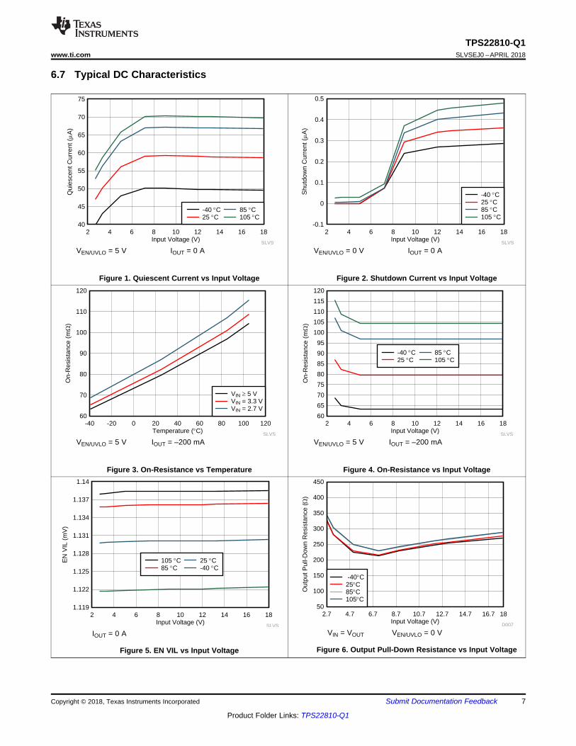
6.7 Typical DC Characteristics
VEN/UVLO = 5 V IOUT = 0 A
Figure 1. Quiescent Current vs Input Voltage
VEN/UVLO = 0 V IOUT = 0 A
Figure 2. Shutdown Current vs Input Voltage
VEN/UVLO = 5 V IOUT = –200 mA
Figure 3. On-Resistance vs Temperature
VEN/UVLO = 5 V IOUT = –200 mA
Figure 4. On-Resistance vs Input Voltage
IOUT = 0 A
Figure 5. EN VIL vs Input Voltage
VIN = VOUT VEN/UVLO = 0 V
Figure 6. Output Pull-Down Resistance vs Input Voltage

VIN
VON
VOUT
IIN
Input Voltage (V)
Tur
non
Tim
e (t
ON)
(Ps)
2.7 4.7 6.7 8.7 10.7 12.7 14.7 16.7 18100
150
200
250
300
350
400
450
500
550
600
D012
-40qC25qC85qC105qC
Input Voltage (V)
VO
UT F
all T
ime
(tF)
(P
s)
2.7 4.7 6.7 8.7 10.7 12.7 14.7 16.7 180
0.2
0.4
0.6
0.8
1
1.2
1.4
1.6
1.8
D010
-40qC25qC85qC105qC
Input Voltage (V)
Tur
noff
Tim
e (t
OF
F)
(Ps)
2.7 4.7 6.7 8.7 10.7 12.7 14.7 16.7 180
0.5
1
1.5
2
2.5
3
3.5
4
4.5
5
D011
-40qC25qC85qC105qC
Input Voltage (V)
VO
UT R
ise
Tim
e (t
R)
(Ps)
2.7 4.7 6.7 8.7 10.7 12.7 14.7 16.7 1850
100150200250300350400450500550600650700750
D008
-40qC25qC85qC105qC
Input Voltage (V)
Del
ay T
ime
(tD)
(Ps)
2.7 4.7 6.7 8.7 10.7 12.7 14.7 16.7 180
20
40
60
80
100
120
140
160
180
200
D009
-40qC25qC85qC105qC
8
TPS22810-Q1SLVSEJ0 –APRIL 2018 www.ti.com
Product Folder Links: TPS22810-Q1
Submit Documentation Feedback Copyright © 2018, Texas Instruments Incorporated
6.8 Typical AC Characteristics
CIN = 1 µF RL = 10 Ω CL = 0.1 µFCT = 2200 pF
Figure 7. VOUT Rise Time (tR) vs Input Voltage
CIN = 1 µF RL = 10 Ω CL = 0.1 µFCT = 2200 pF
Figure 8. Delay Time (tD) vs Input Voltage
CIN = 1 µF RL = 10 Ω CL = 0.1 µF
Figure 9. VOUT Fall Time (tF) vs Input Voltage
CIN = 1 µF RL = 10 Ω CL = 0.1 µF
Figure 10. Turnoff Time (tOFF) vs Input Voltage
CIN = 1 µF RL = 10 Ω CL = 0.1 µFCT = 2200 pF
Figure 11. Turnon Time (tON) vs Input Voltage
VIN = 5 V CIN = 1 µF CL = 0.1 µFRL = 10 Ω CT = 2200 pF
Figure 12. Rise Time tR at VIN = 5 V
VIN
VON
VOUT
IIN
VIN
VON
VOUT
IIN
VIN
VON
VOUT
IIN
9
TPS22810-Q1www.ti.com SLVSEJ0 –APRIL 2018
Product Folder Links: TPS22810-Q1
Submit Documentation FeedbackCopyright © 2018, Texas Instruments Incorporated
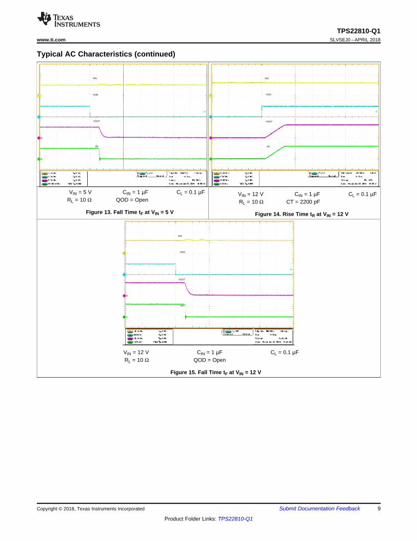
Typical AC Characteristics (continued)
VIN = 5 V CIN = 1 µF CL = 0.1 µFRL = 10 Ω QOD = Open
Figure 13. Fall Time tF at VIN = 5 V
VIN = 12 V CIN = 1 µF CL = 0.1 µFRL = 10 Ω CT = 2200 pF
Figure 14. Rise Time tR at VIN = 12 V
VIN = 12 V CIN = 1 µF CL = 0.1 µFRL = 10 Ω QOD = Open
Figure 15. Fall Time tF at VIN = 12 V

tR
VOUT
10%
90% 90%
100%10%
VOUT
tFtOFF
VON
tOUT
tD
50% 50%
50% 50%
OFF
ON(A) EN/UVLO
GND
VIN
CIN = 1 µF
GND
VOUT
CL
RL
GND
TPS22810
+
-
10
TPS22810-Q1SLVSEJ0 –APRIL 2018 www.ti.com
Product Folder Links: TPS22810-Q1
Submit Documentation Feedback Copyright © 2018, Texas Instruments Incorporated
7 Parameter Measurement Information
A. Rise and fall times of the control signal are 100 ns
Figure 16. Test Circuit
Figure 17. Timing Waveforms

Charge Pump
VIN
EN/UVLO
VOUT
GND
CT
Control Logic
2.54 V
2.4 V
1.23 V
1.13 V ThermalShutdown
QOD
11
TPS22810-Q1www.ti.com SLVSEJ0 –APRIL 2018
Product Folder Links: TPS22810-Q1
Submit Documentation FeedbackCopyright © 2018, Texas Instruments Incorporated
8 Detailed Description
8.1 OverviewThe TPS22810-Q1 is a 6-pin, 2.7-18-V load switch with thermal protection. To reduce voltage drop for lowvoltage and high current rails, the device implements a low resistance N-channel MOSFET which reduces thedrop out voltage across the device.
The device starts its operation by monitoring the VIN bus. When VIN exceeds the undervoltage-lockout threshold(VUVR), the device samples the EN/UVLO pin. A high level on this pin enables the internal MOSFET. When VINrises, the internal MOSFET of the device starts conducting and allow current to flow from VIN to VOUT. WhenEN/UVLO is held low (below VENF), internal MOSFET is turned off.
A voltage VEN/UVLO < VENF on this pin turns off the internal FET, thus disconnecting VIN from VOUT, while voltagebelow VSHUTF takes the device into shutdown mode, with IQ less than 1 μA to ensure minimal power loss.
The device has a configurable slew rate which helps reduce or eliminate power supply droop because of largeinrush currents. The device also features a QOD (Quick Output Discharge) pin with an internal pull-downresistance (RPD) which can be used to discharge VOUT once the switch is disabled.
During shutdown, the device has very low leakage currents, thereby reducing unnecessary leakages fordownstream modules during standby. Integrated control logic, driver, charge pump, and output discharge FETeliminates the need for any external components which reduces solution size and bill of materials (BOM) count.
The device has a thermal protection feature to protect itself against thermal damage due to overtemperature andovercurrent conditions. Safe Operating Area (SOA) requirements are thus inherently met without any specialdesign consideration by the board designer.
8.2 Functional Block Diagram

12
TPS22810-Q1SLVSEJ0 –APRIL 2018 www.ti.com
Product Folder Links: TPS22810-Q1
Submit Documentation Feedback Copyright © 2018, Texas Instruments Incorporated
8.3 Feature Description
8.3.1 On and Off ControlThe EN/UVLO pin controls the state of the switch. EN/UVLO is active high and has a low threshold that caninterface with low-voltage signals. The EN/UVLO pin is compatible with standard GPIO logic threshold. It can beused with any microcontroller with 1.2 V or higher GPIO voltage. This pin cannot be left floating and must bedriven either high or low for proper functionality.
8.3.2 Quick Output Discharge (QOD)The TPS22810-Q1 includes a QOD feature. The QOD pin can be configured in one of three ways:• QOD pin shorted to VOUT pin. Using this method, the discharge rate after the switch becomes disabled is
controlled with the value of the internal pull-down resistance (RPD). The value of this resistance is listed in theElectrical Characteristics table.
• QOD pin connected to VOUT pin using an external resistor REXT. After the switch becomes disabled, thedischarge rate is controlled by the value of the total resistance of the QOD. To adjust the total QODresistance, Equation 1 can be used.
RQOD = RPD + REXT
where• RQOD is the total output discharge resistance• RPD is the internal pulldown resistance• REXT is the external resistance placed between the VOUT and QOD pin. (1)
• QOD pin is unused and left floating. Using this method, there is no quick output discharge functionality, andthe output remains floating after the switch is disabled.
Note that during thermal shutdown, the QOD functionality is not available. The device does not discharge theload because RPD does not become engaged.
The fall times of the device depend on many factors including the total resistance of the QOD, VIN, and theoutput capacitance. When QOD is connected to VOUT, the fall time changes over VIN because the internal RPDvaries over VIN. To calculate the approximate fall time of VOUT for a given RQOD, use Equation 2 and Table 1.
VCAP = VIN × e-t/τ
where• VCAP is the voltage across the capacitor (V)• t is the time since power supply removal (s)• τ is the time constant equal to RQOD × CL (2)
The fall time's dependency on VIN becomes minimal because the QOD value increases with additional externalresistance. See Table 1 for QOD fall times.
(1) TYPICAL VALUES WITH QOD SHORTED TO VOUT
Table 1. QOD Fall Times
VIN (V)FALL TIME (μs) 90% - 10%, CIN = 1 μF, IOUT = 0 A , VIN = 0 V, ON = 0 V (1)
TA = 25°C TA = 85°CCL = 1 μF CL = 10 μF CL = 100 μF CL = 1 μF CL = 10 μF CL = 100 μF
18 470 4700 47000 470 4700 4700012 450 4500 45000 450 4500 450009 440 4400 44000 440 4400 440005 500 5000 50000 480 4800 48000
3.3 600 6000 60000 570 5700 57000

VIN VOUT
ThermalShutdown
2.54 V2.4 V
1.23 V1.13 V
CL
VIN
EN/UVLO
GND
R2
R1
GateControl
CIN
13
TPS22810-Q1www.ti.com SLVSEJ0 –APRIL 2018
Product Folder Links: TPS22810-Q1
Submit Documentation FeedbackCopyright © 2018, Texas Instruments Incorporated
8.3.2.1 QOD when System Power is RemovedThe adjustable QOD can be used to control the power down sequencing of a system even when the systempower supply is removed. When the power is removed, the input capacitor, CIN, discharges at VIN. Past the setUVLO level, the pull-down resistance RPD becomes disabled and the output no longer becomes discharged. Ifthere is still remaining charge on the output capacitor, this results in longer fall times. Care must be taken suchthat CIN is large enough to meet the device UVLO settings.
8.3.2.2 Internal QOD ConsiderationsSpecial considerations must be taken when using the internal RPD by shorting the QOD pin to the VOUT pin. Theinternal RPD is a pull-down resistance designed to quickly discharge a load after the switch has been disabled.Care must be used to ensure that excessive current does not flow through RPD during discharge so that themaximum TJ of 125°C is not exceeded. When using only the internal RPD to discharge a load, the total capacitiveload must not exceed 200 uF. Otherwise, an external resistor, REXT must be used to ensure the amount ofcurrent flowing through RPD is properly limited and the maximum TJ is not exceeded. To ensure the device is notdamaged, the remaining charge from CL must decay naturally through the internal QOD resistance and must notbe driven.
8.3.3 EN/UVLOEN/UVLO controls the ON and OFF state of the internal MOSFET, as an input pin. In its high state, the internalMOSFET is enabled. A low on this pin turns off the internal MOSFET. High and Low levels are specified in theparametric table of the datasheet.
A voltage VEN/UVLO < VENF on this pin turns off the internal FET, thus disconnecting VIN from VOUT, while voltagebelow VSHUTF takes the device into shutdown mode, with IQ less than 1 μA to ensure minimal power loss.
The EN/UVLO pin can be directly driven by a 1.8 V, 3.3 V or 5 V general purpose output pin.
The internal de-glitch delay on EN/UVLO falling edge is intentionally kept low (2.5 μs typical) for quick detectionof power failure. For applications where a higher de-glitch delay on EN/UVLO is desired, or when the supply isparticularly noisy, it is recommended to use an external bypass capacitor from EN/UVLO to GND.
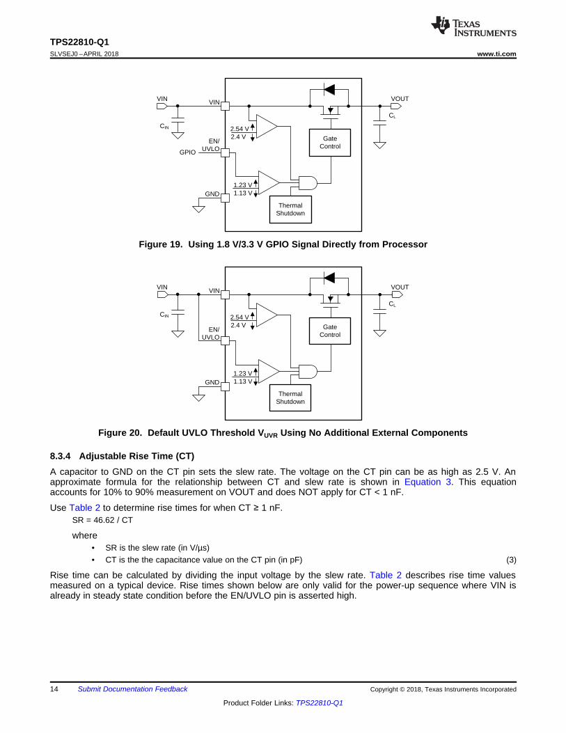
The undervoltage lock out (UVLO) threshold can be programmed by using an external resistor divider fromsupply VIN terminal to EN/UVLO terminal to GND shown in Figure 18. When an undervoltage or input power failevent is detected, the internal FET is quickly turned off. If the programmable UVLO function is not needed, theEN/UVLO terminal must be connected to the VIN terminal. EN/UVLO terminal must not be left floating.
The device also implements internal UVLO circuitry on the VIN terminal. The device disables when the VINterminal voltage falls below internal UVLO Threshold (VUVF). The internal UVLO threshold has a hysteresis(VUVRhyst). See Figure 19 and Figure 20.
Figure 18. Configuring UVLO with External Resistor Network
VIN VOUT
ThermalShutdown
2.54 V2.4 V
1.23 V1.13 V
CL
VIN
EN/UVLO
GND
GateControl
CIN
VIN VOUT
ThermalShutdown
2.54 V2.4 V
1.23 V1.13 V
CL
VIN
EN/UVLO
GND
GateControl
CIN
GPIO
14
TPS22810-Q1SLVSEJ0 –APRIL 2018 www.ti.com
Product Folder Links: TPS22810-Q1
Submit Documentation Feedback Copyright © 2018, Texas Instruments Incorporated
Figure 19. Using 1.8 V/3.3 V GPIO Signal Directly from Processor
Figure 20. Default UVLO Threshold VUVR Using No Additional External Components
8.3.4 Adjustable Rise Time (CT)A capacitor to GND on the CT pin sets the slew rate. The voltage on the CT pin can be as high as 2.5 V. Anapproximate formula for the relationship between CT and slew rate is shown in Equation 3. This equationaccounts for 10% to 90% measurement on VOUT and does NOT apply for CT < 1 nF.
Use Table 2 to determine rise times for when CT ≥ 1 nF.SR = 46.62 / CT
where• SR is the slew rate (in V/µs)• CT is the the capacitance value on the CT pin (in pF) (3)
Rise time can be calculated by dividing the input voltage by the slew rate. Table 2 describes rise time valuesmeasured on a typical device. Rise times shown below are only valid for the power-up sequence where VIN isalready in steady state condition before the EN/UVLO pin is asserted high.
15
TPS22810-Q1www.ti.com SLVSEJ0 –APRIL 2018
Product Folder Links: TPS22810-Q1
Submit Documentation FeedbackCopyright © 2018, Texas Instruments Incorporated
Table 2. Rise Time Table
CT (pF)RISE TIME (µs) 10% - 90%, CL = 0.1 µF, CIN = 1 µF, RL = 10 Ω
VIN = 18 V VIN = 12 V VIN = 9 V VIN = 5 V VIN = 3.3 V0 115 91 78 60 98
470 136 94 80 63 981000 310 209 158 91 1022200 688 464 345 198 1354700 1430 957 704 397 265
10000 3115 2085 1540 864 55027000 8230 5460 4010 2245 1430
8.3.5 Thermal ShutdownThe switch disables when the junction temperature (TJ) rises above the thermal shutdown threshold, TSD. Theswitch re-enables once the temperature drops below the TSD – TSD,HYS value.
8.4 Device Functional ModesThe features of the TPS22810-Q1 depend on the operating mode. Table 3 summarizes the Device FunctionalModes.
Table 3. Function TableEN/UVLO Device State
L DisabledH Enabled

PowerSupply
EN/UVLO
GND
VIN
CT
VOUT
OFF
ON
TPS22810
QOD
CL RLCIN
16
TPS22810-Q1SLVSEJ0 –APRIL 2018 www.ti.com
Product Folder Links: TPS22810-Q1
Submit Documentation Feedback Copyright © 2018, Texas Instruments Incorporated
9 Application and Implementation
NOTEInformation in the following applications sections is not part of the TI componentspecification, and TI does not warrant its accuracy or completeness. TI’s customers areresponsible for determining suitability of components for their purposes. Customers shouldvalidate and test their design implementation to confirm system functionality.
9.1 Application InformationThis section highlights some of the design considerations when implementing this device in various applications.A PSPICE model for this device is also available in the product page of this device on www.ti.com (See theDevice Support section for more information).
9.1.1 ON and OFF ControlThe EN/UVLO pin controls the state of the switch. Asserting EN/UVLO high enables the switch. EN/UVLO isactive high and has a low threshold that can interface with low-voltage signals. The EN/UVLO pin is compatiblewith standard GPIO logic thresholds. It can be used with any microcontroller with 1.2 V or higher GPIO voltage.This pin cannot be left floating and must be driven either high or low for proper functionality.
9.1.2 Input Capacitor (Optional)To limit the voltage drop on the input supply caused by transient inrush currents when the switch turns on into adischarged load capacitor, a capacitor must be placed between VIN and GND. A 1-μF ceramic capacitor, CIN,placed close to the pins, is usually sufficient. Higher values of CIN can be used to further reduce the voltage dropduring high current applications. When switching heavy loads, it is recommended to have an input capacitorabout 10 times higher than the output capacitor to avoid excessive voltage drop.
9.1.3 Output Capacitor (Optional)Due to the integrated body diode in the NMOS switch, a CIN greater than CL is highly recommended. A CLgreater than CIN can cause VOUT to exceed VIN when the system supply is removed. This can result in currentflow through the body diode from VOUT to VIN. A CIN to CL ratio of 10 to 1 is recommended for minimizing VINdip caused by inrush currents during startup; however, a 10 to 1 ratio for capacitance is not required for properfunctionality of the device. A ratio smaller than 10 to 1 (such as 1 to 1) can cause slightly more VIN dip uponturnon due to inrush currents.
This can be mitigated by increasing the capacitance on the CT pin for a longer rise time.
9.2 Typical ApplicationThis typical application demonstrates how the TPS22810-Q1 can be used to power downstream modules.
Figure 21. Typical Application Schematic

QOD(20ms)/(R (22 F))1.2V 10.8V e u P u
17
TPS22810-Q1www.ti.com SLVSEJ0 –APRIL 2018
Product Folder Links: TPS22810-Q1
Submit Documentation FeedbackCopyright © 2018, Texas Instruments Incorporated
Typical Application (continued)9.2.1 Design RequirementsFor this design example, use the values listed in Table 4:
Table 4. Design ParametersDESIGN PARAMETER EXAMPLE VALUE
VIN 12 VLoad current 2 A
CL 22 µFDesired fall time 20 ms
Maximum acceptable inrush current 400 mA
9.2.2 Detailed Design Procedure
9.2.2.1 Shutdown Sequencing During Unexpected Power LossUsing the adjustable Quick Output Discharge function of the TPS22810-Q1, adding a load switch to each powerrail can be used to manage the power down sequencing in the event of an unexpected power loss (for example,battery removal). To determine the QOD values for each load switch, first confirm the power down order of thedevice you wish to power sequence. Be sure to check if there are voltage or timing margins that must bemaintained during power down. Next, consult Table 1 to determine appropriate CL and RQOD values for eachpower rail's load switch so that the load switches' fall times correspond to the order in which they need to bepowered down. In the above example, we must have this power rail's fall time to be 4 ms. Using Equation 2, wecan determine the appropriate RQOD to achieve our desired fall time.
Since fall times are measured from 90% of VOUT to 10% of VOUT, using Equation 2, we get Equation 4 andEquation 5.
(4)RQOD = 413.7 Ω (5)
Consulting Figure 6, RPD at VIN = 12 V is approximately 250 Ω. Using Equation 1, the required external QODresistance can be calculated shown in Equation 6 and Equation 7.
413.7 Ω = 250 Ω + REXT (6)REXT = 163.7 Ω (7)
Figure 22 through Figure 25 are scope shots demonstrating an example of the QOD functionality when power isremoved from the device (both ON and VIN are disconnected simultaneously). In the scope shots, the VIN = 12 Vand correspond to when RQOD = 1000 Ω, RQOD= 500 Ω, and QOD = VOUT with two values of CL = 10 µF and 22µF.

VIN
VON
VOUT
VIN
VON
VOUT
VIN
VON
VOUT
VIN
VON
VOUT
18
TPS22810-Q1SLVSEJ0 –APRIL 2018 www.ti.com
Product Folder Links: TPS22810-Q1
Submit Documentation Feedback Copyright © 2018, Texas Instruments Incorporated
VIN = 12 V CIN = 1 µF CL = 10 µF
Figure 22. Fall Time tF at VIN = 12 V, RQOD = 1000 Ω
VIN = 12 V CIN = 1 µF CL = 10 µF
Figure 23. Fall Time tF at VIN = 12 V, RQOD = 500 Ω
VIN = 12 V CIN = 1 µF CL = 10 µF
Figure 24. tF at VIN = 12 V , QOD = VOUT
VIN = 12 V CIN = 1 µF CL = 22 µF
Figure 25. tF at VIN = 12 V, RQOD = 1000 Ω

OUTINRUSH L
dVI C
dt= ´
VIN
VON
VOUT
VIN
VON
VOUT
19
TPS22810-Q1www.ti.com SLVSEJ0 –APRIL 2018
Product Folder Links: TPS22810-Q1
Submit Documentation FeedbackCopyright © 2018, Texas Instruments Incorporated
VIN = 12 V CIN = 1 µF CL = 22 µF
Figure 26. tF at VIN = 12 V, RQOD = 500 Ω
VIN = 12 V CIN = 1 µF CL = 22 µF
Figure 27. tF at VIN = 12 V, QOD = VOUT
9.2.2.2 VIN to VOUT Voltage DropThe VIN to VOUT voltage drop in the device is determined by the RON of the device and the load current. TheRON of the device depends upon the VIN conditions of the device. Refer to the RON specification of the device inthe Electrical Characteristics table of this datasheet. Once the RON of the device is determined based upon theVIN conditions, use Equation 8 to calculate the VIN to VOUT voltage drop.
∆V = ILOAD × RON
where• ΔV is the voltage drop from VIN to VOUT• ILOAD is the load current• RON is the On-resistance of the device for a specific VIN (8)
An appropriate ILOAD must be chosen such that the IMAX specification of the device is not violated.
9.2.2.3 Inrush CurrentTo determine how much inrush current is caused by the CL capacitor, use Equation 9.
where• IINRUSH is the amount of inrush caused by CL
• CL is the capacitance on VOUT• dt is the Output Voltage rise time during the ramp up of VOUT when the device is enabled• dVOUT is the change in VOUT during the ramp up of VOUT when the device is enabled (9)
The appropriate rise time can be calculated using the design requirements and the inrush current equation.When we calculate the rise time (measured from 10% to 90% of VOUT), we account for this in our dVOUTparameter (80% of VOUT = 9.6 V) shown in Equation 10 and Equation 11.
400 mA = 22 µF × 9.6 V/dt (10)dt = 528 µs (11)
To ensure an inrush current of less than 400 mA, choose a CT value that yields a rise time of more than 528 μs.Consulting Table 2 at VIN = 12 V, CT = 4700 pF provides a typical rise time of 957 μs. Using this rise time andvoltage into Equation 9, yields Equation 12 and Equation 13.
IInrush = 22 µF × 9.6 V/ 957 µs (12)Inrush = 220 mA (13)
VIN
VON
VOUT
IIN
VIN
VON
VOUT
IIN
VIN
VON
VOUT
IIN
VIN
VON
VOUT
IIN
20
TPS22810-Q1SLVSEJ0 –APRIL 2018 www.ti.com
Product Folder Links: TPS22810-Q1
Submit Documentation Feedback Copyright © 2018, Texas Instruments Incorporated
An appropriate CL value must be placed on VOUT such that the IMAX and IPLS specifications of the device are notviolated.
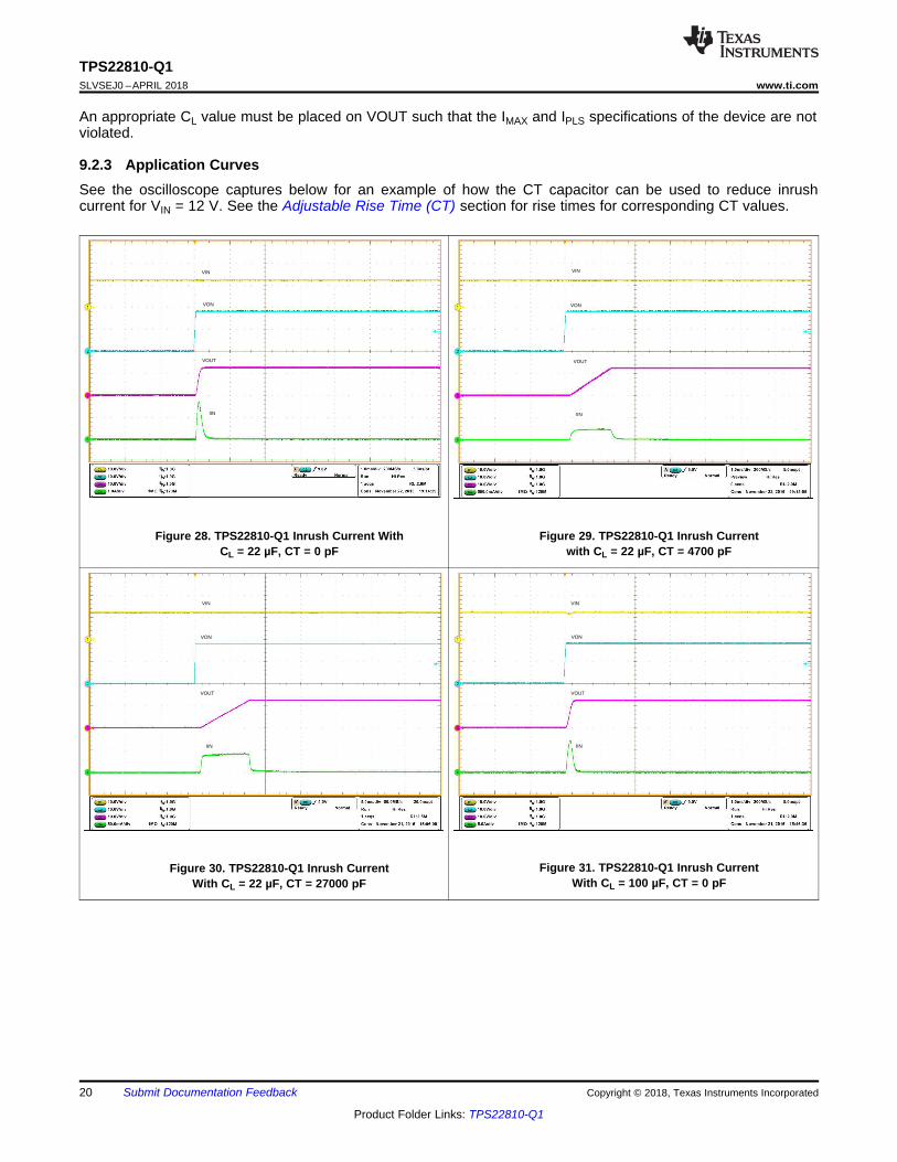
9.2.3 Application CurvesSee the oscilloscope captures below for an example of how the CT capacitor can be used to reduce inrushcurrent for VIN = 12 V. See the Adjustable Rise Time (CT) section for rise times for corresponding CT values.
Figure 28. TPS22810-Q1 Inrush Current WithCL = 22 µF, CT = 0 pF
Figure 29. TPS22810-Q1 Inrush Currentwith CL = 22 µF, CT = 4700 pF
Figure 30. TPS22810-Q1 Inrush CurrentWith CL = 22 µF, CT = 27000 pF
Figure 31. TPS22810-Q1 Inrush CurrentWith CL = 100 µF, CT = 0 pF

VIN
VON
VOUT
IIN
VIN
VON
VOUT
IIN
21
TPS22810-Q1www.ti.com SLVSEJ0 –APRIL 2018
Product Folder Links: TPS22810-Q1
Submit Documentation FeedbackCopyright © 2018, Texas Instruments Incorporated
Figure 32. TPS22810-Q1 Inrush CurrentWith CL = 100 µF, CT = 4700 pF
Figure 33. TPS22810-Q1 Inrush CurrentWith CL = 100 µF, CT = 27000 pF
10 Power Supply RecommendationsThe device is designed to operate from a VIN range of 2.7 V to 18 V. This supply must be well regulated andplaced as close to the device terminal as possible with the recommended 1-µF bypass capacitor. If the supply islocated more than a few inches from the device terminals, additional bulk capacitance may be required inaddition to the ceramic bypass capacitors. If additional bulk capacitance is required, an electrolytic, tantalum, orceramic capacitor of 1-µF may be sufficient.
The TPS22810-Q1 operates regardless of power sequencing order. The order in which voltages are applied toVIN and EN/UVLO does not damage the device as long as the voltages do not exceed the absolute maximumoperating conditions.

J(MAX) AD(MAX)
JA
T TP
-=
q
1 VOUT
2 QOD
3 CT 4EN/UVLO
5GND
6VIN
VIA to Power Ground Plane
22
TPS22810-Q1SLVSEJ0 –APRIL 2018 www.ti.com
Product Folder Links: TPS22810-Q1
Submit Documentation Feedback Copyright © 2018, Texas Instruments Incorporated
11 Layout
11.1 Layout Guidelines1. VIN and VOUT traces must be as short and wide as possible to accommodate for high current.2. The VIN pin must be bypassed to ground with low ESR ceramic bypass capacitors. The typical
recommended bypass capacitance is 1-μF ceramic with X5R or X7R dielectric. This capacitor must beplaced as close to the device pins as possible.
11.2 Layout Example
Figure 34. Recommended Board Layout
11.3 Thermal ConsiderationsFor best performance, all traces must be as short as possible. To be most effective, the input and outputcapacitors must be placed close to the device to minimize the effects that parasitic trace inductances may haveon normal and short-circuit operation. Using wide traces for VIN, VOUT, and GND helps minimize the parasiticelectrical effects along with minimizing the case to ambient thermal impedance.
The maximum IC junction temperature must be restricted to 150°C under normal operating conditions. Tocalculate the maximum allowable dissipation, PD(max) for a given output current and ambient temperature, useEquation 14.
where• PD(MAX) is the maximum allowable power dissipation• TJ(MAX) is the maximum allowable junction temperature (150°C for the TPS22810-Q1)• TA is the ambient temperature of the device• θJA is the junction to air thermal impedance. Refer to the Thermal Information table. This parameter highly
depends on the board layout. (14)

23
TPS22810-Q1www.ti.com SLVSEJ0 –APRIL 2018
Product Folder Links: TPS22810-Q1
Submit Documentation FeedbackCopyright © 2018, Texas Instruments Incorporated
12 Device and Documentation Support
12.1 Device Support
12.1.1 Developmental SupportFor the TPS22810 PSpice Transient Model, see TPS22810 PSpice Transient Model
12.2 Documentation Support
12.2.1 Related DocumentationFor related documentation see the following:• TPS22810 Load Switch Evaluation Module• Selecting a Load Switch to Replace a Discrete Solution• Timing of Load Switches
12.3 Receiving Notification of Documentation UpdatesTo receive notification of documentation updates—including silicon errata—go to the product folder for yourdevice on ti.com. In the upper right corner, click the Alert me button. This registers you to receive a weekly digestof product information that has changed (if any). For change details, check the revision history of any reviseddocument.
12.4 Community ResourcesThe following links connect to TI community resources. Linked contents are provided "AS IS" by the respectivecontributors. They do not constitute TI specifications and do not necessarily reflect TI's views; see TI's Terms ofUse.
TI E2E™ Online Community TI's Engineer-to-Engineer (E2E) Community. Created to foster collaborationamong engineers. At e2e.ti.com, you can ask questions, share knowledge, explore ideas and helpsolve problems with fellow engineers.
Design Support TI's Design Support Quickly find helpful E2E forums along with design support tools andcontact information for technical support.
12.5 TrademarksE2E is a trademark of Texas Instruments.All other trademarks are the property of their respective owners.
12.6 Electrostatic Discharge CautionThis integrated circuit can be damaged by ESD. Texas Instruments recommends that all integrated circuits be handled withappropriate precautions. Failure to observe proper handling and installation procedures can cause damage.
ESD damage can range from subtle performance degradation to complete device failure. Precision integrated circuits may be moresusceptible to damage because very small parametric changes could cause the device not to meet its published specifications.
12.7 GlossarySLYZ022 — TI Glossary.
This glossary lists and explains terms, acronyms, and definitions.
13 Mechanical, Packaging, and Orderable InformationThe following pages include mechanical, packaging, and orderable information. This information is the mostcurrent data available for the designated devices. This data is subject to change without notice and revision ofthis document. For browser-based versions of this data sheet, refer to the left-hand navigation.

PACKAGE OPTION ADDENDUM
www.ti.com 6-Apr-2018
Addendum-Page 1
PACKAGING INFORMATION
Orderable Device Status(1)
Package Type PackageDrawing
Pins PackageQty
Eco Plan(2)
Lead/Ball Finish(6)
MSL Peak Temp(3)
Op Temp (°C) Device Marking(4/5)
Samples
TPS22810TDBVRQ1 ACTIVE SOT-23 DBV 6 3000 Green (RoHS& no Sb/Br)
CU NIPDAU Level-2-260C-1 YEAR -40 to 105 1EFF
(1) The marketing status values are defined as follows:ACTIVE: Product device recommended for new designs.LIFEBUY: TI has announced that the device will be discontinued, and a lifetime-buy period is in effect.NRND: Not recommended for new designs. Device is in production to support existing customers, but TI does not recommend using this part in a new design.PREVIEW: Device has been announced but is not in production. Samples may or may not be available.OBSOLETE: TI has discontinued the production of the device.
(2) RoHS: TI defines "RoHS" to mean semiconductor products that are compliant with the current EU RoHS requirements for all 10 RoHS substances, including the requirement that RoHS substancedo not exceed 0.1% by weight in homogeneous materials. Where designed to be soldered at high temperatures, "RoHS" products are suitable for use in specified lead-free processes. TI mayreference these types of products as "Pb-Free".RoHS Exempt: TI defines "RoHS Exempt" to mean products that contain lead but are compliant with EU RoHS pursuant to a specific EU RoHS exemption.Green: TI defines "Green" to mean the content of Chlorine (Cl) and Bromine (Br) based flame retardants meet JS709B low halogen requirements of <=1000ppm threshold. Antimony trioxide basedflame retardants must also meet the <=1000ppm threshold requirement.
(3) MSL, Peak Temp. - The Moisture Sensitivity Level rating according to the JEDEC industry standard classifications, and peak solder temperature.
(4) There may be additional marking, which relates to the logo, the lot trace code information, or the environmental category on the device.
(5) Multiple Device Markings will be inside parentheses. Only one Device Marking contained in parentheses and separated by a "~" will appear on a device. If a line is indented then it is a continuationof the previous line and the two combined represent the entire Device Marking for that device.
(6) Lead/Ball Finish - Orderable Devices may have multiple material finish options. Finish options are separated by a vertical ruled line. Lead/Ball Finish values may wrap to two lines if the finishvalue exceeds the maximum column width.
Important Information and Disclaimer:The information provided on this page represents TI's knowledge and belief as of the date that it is provided. TI bases its knowledge and belief on informationprovided by third parties, and makes no representation or warranty as to the accuracy of such information. Efforts are underway to better integrate information from third parties. TI has taken andcontinues to take reasonable steps to provide representative and accurate information but may not have conducted destructive testing or chemical analysis on incoming materials and chemicals.TI and TI suppliers consider certain information to be proprietary, and thus CAS numbers and other limited information may not be available for release.
In no event shall TI's liability arising out of such information exceed the total purchase price of the TI part(s) at issue in this document sold by TI to Customer on an annual basis.
OTHER QUALIFIED VERSIONS OF TPS22810-Q1 :

PACKAGE OPTION ADDENDUM
www.ti.com 6-Apr-2018
Addendum-Page 2
• Catalog: TPS22810
NOTE: Qualified Version Definitions:
• Catalog - TI's standard catalog product
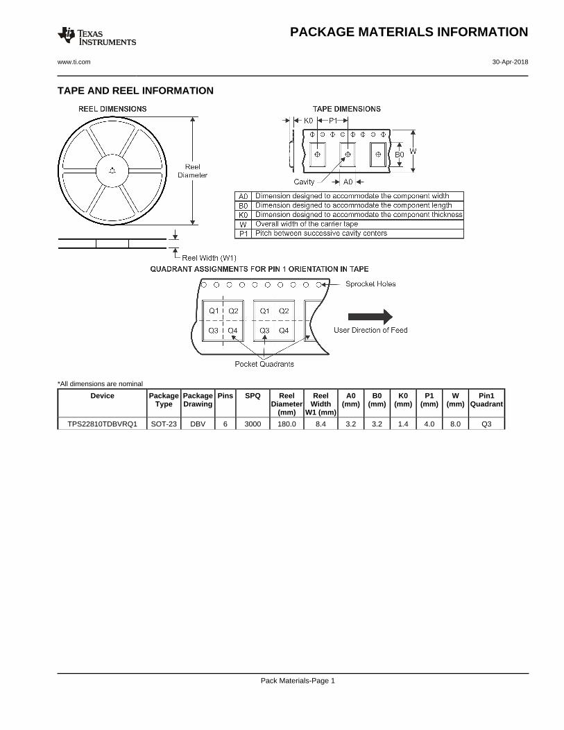
TAPE AND REEL INFORMATION
*All dimensions are nominal
Device PackageType
PackageDrawing
Pins SPQ ReelDiameter
(mm)
ReelWidth
W1 (mm)
A0(mm)
B0(mm)
K0(mm)
P1(mm)
W(mm)
Pin1Quadrant
TPS22810TDBVRQ1 SOT-23 DBV 6 3000 180.0 8.4 3.2 3.2 1.4 4.0 8.0 Q3
PACKAGE MATERIALS INFORMATION
www.ti.com 30-Apr-2018
Pack Materials-Page 1

*All dimensions are nominal
Device Package Type Package Drawing Pins SPQ Length (mm) Width (mm) Height (mm)
TPS22810TDBVRQ1 SOT-23 DBV 6 3000 210.0 185.0 35.0
PACKAGE MATERIALS INFORMATION
www.ti.com 30-Apr-2018
Pack Materials-Page 2


IMPORTANT NOTICE
Texas Instruments Incorporated (TI) reserves the right to make corrections, enhancements, improvements and other changes to itssemiconductor products and services per JESD46, latest issue, and to discontinue any product or service per JESD48, latest issue. Buyersshould obtain the latest relevant information before placing orders and should verify that such information is current and complete.TI’s published terms of sale for semiconductor products (http://www.ti.com/sc/docs/stdterms.htm) apply to the sale of packaged integratedcircuit products that TI has qualified and released to market. Additional terms may apply to the use or sale of other types of TI products andservices.Reproduction of significant portions of TI information in TI data sheets is permissible only if reproduction is without alteration and isaccompanied by all associated warranties, conditions, limitations, and notices. TI is not responsible or liable for such reproduceddocumentation. Information of third parties may be subject to additional restrictions. Resale of TI products or services with statementsdifferent from or beyond the parameters stated by TI for that product or service voids all express and any implied warranties for theassociated TI product or service and is an unfair and deceptive business practice. TI is not responsible or liable for any such statements.Buyers and others who are developing systems that incorporate TI products (collectively, “Designers”) understand and agree that Designersremain responsible for using their independent analysis, evaluation and judgment in designing their applications and that Designers havefull and exclusive responsibility to assure the safety of Designers' applications and compliance of their applications (and of all TI productsused in or for Designers’ applications) with all applicable regulations, laws and other applicable requirements. Designer represents that, withrespect to their applications, Designer has all the necessary expertise to create and implement safeguards that (1) anticipate dangerousconsequences of failures, (2) monitor failures and their consequences, and (3) lessen the likelihood of failures that might cause harm andtake appropriate actions. Designer agrees that prior to using or distributing any applications that include TI products, Designer willthoroughly test such applications and the functionality of such TI products as used in such applications.TI’s provision of technical, application or other design advice, quality characterization, reliability data or other services or information,including, but not limited to, reference designs and materials relating to evaluation modules, (collectively, “TI Resources”) are intended toassist designers who are developing applications that incorporate TI products; by downloading, accessing or using TI Resources in anyway, Designer (individually or, if Designer is acting on behalf of a company, Designer’s company) agrees to use any particular TI Resourcesolely for this purpose and subject to the terms of this Notice.TI’s provision of TI Resources does not expand or otherwise alter TI’s applicable published warranties or warranty disclaimers for TIproducts, and no additional obligations or liabilities arise from TI providing such TI Resources. TI reserves the right to make corrections,enhancements, improvements and other changes to its TI Resources. TI has not conducted any testing other than that specificallydescribed in the published documentation for a particular TI Resource.Designer is authorized to use, copy and modify any individual TI Resource only in connection with the development of applications thatinclude the TI product(s) identified in such TI Resource. NO OTHER LICENSE, EXPRESS OR IMPLIED, BY ESTOPPEL OR OTHERWISETO ANY OTHER TI INTELLECTUAL PROPERTY RIGHT, AND NO LICENSE TO ANY TECHNOLOGY OR INTELLECTUAL PROPERTYRIGHT OF TI OR ANY THIRD PARTY IS GRANTED HEREIN, including but not limited to any patent right, copyright, mask work right, orother intellectual property right relating to any combination, machine, or process in which TI products or services are used. Informationregarding or referencing third-party products or services does not constitute a license to use such products or services, or a warranty orendorsement thereof. Use of TI Resources may require a license from a third party under the patents or other intellectual property of thethird party, or a license from TI under the patents or other intellectual property of TI.TI RESOURCES ARE PROVIDED “AS IS” AND WITH ALL FAULTS. TI DISCLAIMS ALL OTHER WARRANTIES ORREPRESENTATIONS, EXPRESS OR IMPLIED, REGARDING RESOURCES OR USE THEREOF, INCLUDING BUT NOT LIMITED TOACCURACY OR COMPLETENESS, TITLE, ANY EPIDEMIC FAILURE WARRANTY AND ANY IMPLIED WARRANTIES OFMERCHANTABILITY, FITNESS FOR A PARTICULAR PURPOSE, AND NON-INFRINGEMENT OF ANY THIRD PARTY INTELLECTUALPROPERTY RIGHTS. TI SHALL NOT BE LIABLE FOR AND SHALL NOT DEFEND OR INDEMNIFY DESIGNER AGAINST ANY CLAIM,INCLUDING BUT NOT LIMITED TO ANY INFRINGEMENT CLAIM THAT RELATES TO OR IS BASED ON ANY COMBINATION OFPRODUCTS EVEN IF DESCRIBED IN TI RESOURCES OR OTHERWISE. IN NO EVENT SHALL TI BE LIABLE FOR ANY ACTUAL,DIRECT, SPECIAL, COLLATERAL, INDIRECT, PUNITIVE, INCIDENTAL, CONSEQUENTIAL OR EXEMPLARY DAMAGES INCONNECTION WITH OR ARISING OUT OF TI RESOURCES OR USE THEREOF, AND REGARDLESS OF WHETHER TI HAS BEENADVISED OF THE POSSIBILITY OF SUCH DAMAGES.Unless TI has explicitly designated an individual product as meeting the requirements of a particular industry standard (e.g., ISO/TS 16949and ISO 26262), TI is not responsible for any failure to meet such industry standard requirements.Where TI specifically promotes products as facilitating functional safety or as compliant with industry functional safety standards, suchproducts are intended to help enable customers to design and create their own applications that meet applicable functional safety standardsand requirements. Using products in an application does not by itself establish any safety features in the application. Designers mustensure compliance with safety-related requirements and standards applicable to their applications. Designer may not use any TI products inlife-critical medical equipment unless authorized officers of the parties have executed a special contract specifically governing such use.Life-critical medical equipment is medical equipment where failure of such equipment would cause serious bodily injury or death (e.g., lifesupport, pacemakers, defibrillators, heart pumps, neurostimulators, and implantables). Such equipment includes, without limitation, allmedical devices identified by the U.S. Food and Drug Administration as Class III devices and equivalent classifications outside the U.S.TI may expressly designate certain products as completing a particular qualification (e.g., Q100, Military Grade, or Enhanced Product).Designers agree that it has the necessary expertise to select the product with the appropriate qualification designation for their applicationsand that proper product selection is at Designers’ own risk. Designers are solely responsible for compliance with all legal and regulatoryrequirements in connection with such selection.Designer will fully indemnify TI and its representatives against any damages, costs, losses, and/or liabilities arising out of Designer’s non-compliance with the terms and provisions of this Notice.
Mailing Address: Texas Instruments, Post Office Box 655303, Dallas, Texas 75265Copyright © 2018, Texas Instruments Incorporated