tps6131x 1.5-a multiple led camera flash and video light ... · production data. tps61310, ......
TRANSCRIPT

VOUT
AVIN
SWSW
LED1
PGNDPGND
AGND
SDASCL
LED2
LED3
STRB0
TS
NRESET
INDLED
NTC
STRB1
AGND
Copyright © 2016, Texas Instruments Incorporated
2.5 V to5.5 V
Tx-MASK
GPIO/PG
C
10 mFO D1 D2
PrivacyIndicator
I C I/F2
C
4.7 mFI
L2.2 mH
Product
Folder
Sample &Buy
Technical
Documents
Tools &
Software
Support &Community
An IMPORTANT NOTICE at the end of this data sheet addresses availability, warranty, changes, use in safety-critical applications,intellectual property matters and other important disclaimers. PRODUCTION DATA.
TPS61310, TPS61311SLVS978D –MARCH 2010–REVISED SEPTEMBER 2016
TPS6131x 1.5-A Multiple LED Camera Flash and Video Light DriverWith I2C Compatible Interface
1
1 Features1• Operational Modes:
– Video Light and Flash Strobe– Voltage Regulated Converter: 3.8 V to 5.7 V
With Down Mode– Standby: 2 µA (Typical)
• LED VF Measurement• Power-Save Mode for Improved Efficiency at Low
Output Power, Up to 95% Efficiency• I2C Compatible Interface up to 3.4 Mbps• Dual Wire Camera Module Interface• Zero Latency Tx-Masking Input• Hardware Reset Input• Privacy Indicator LED Output• GPIO and Power Good Output• Various Safe Operation and Robust Handling
Features:– LED Temperature Monitoring– Open and Shorted LED Detection and
Protection– Integrated LED Safety Timer– Automatic Battery Voltage Droop Monitoring
and Protection– Smooth LED Current Ramp-Up and Ramp-
Down– Undervoltage Lockout
• Total Solution Size of Less Than 25 mm2
• Available in a 20-Pin NanoFree™ DSBGAPackage
2 Applications• Single, Dual, or Triple White LED Flash Supply for
Cell Phones and Smart-Phones• Video Lighting for Digital Video Applications• General Lighting Applications• Audio Amplifier Power Supply
3 DescriptionThe TPS6131x family is an integrated solution with awide feature set for driving up to three LEDs for still-camera flash strobe and video-camera lightingapplications. It is based on a high efficiencysynchronous boost topology with combinable currentsinks to drive up to three white LEDs in parallel. The2-MHz switching frequency allows the use of smalland low-profile 2.2-µH inductors. To optimize overallefficiency, the device operates with a low LED-feedback voltage and regulated output-voltageadaptation.
The device integrates a control scheme thatautomatically optimizes the LED current flash budgetas a function of the battery voltage condition.
The TPS6131x not only operates as a regulatedcurrent source, but also as a standard voltage boostregulator. The device enters power-save modeoperation at light load currents to maintain highefficiency over the entire load current range. Theseoperating modes can be useful to supply other highpower devices in the system (for example, a hands-free audio PA).
To simplify video light and flash synchronization withthe camera module, the device offers a dedicatedcontrol interface (STRB0, STRB1) for zero latencyLED turnon time.
Device Information(1)
PART NUMBER PACKAGE BODY SIZE (NOM)TPS61310,TPS61311 DSBGA (20) 2.20 mm × 1.90 mm
(1) For all available packages, see the orderable addendum atthe end of the data sheet.
Typical Application
2
TPS61310, TPS61311SLVS978D –MARCH 2010–REVISED SEPTEMBER 2016 www.ti.com
Product Folder Links: TPS61310 TPS61311
Submit Documentation Feedback Copyright © 2010–2016, Texas Instruments Incorporated
Table of Contents1 Features .................................................................. 12 Applications ........................................................... 13 Description ............................................................. 14 Revision History..................................................... 25 Device Comparison Table ..................................... 36 Pin Configuration and Functions ......................... 37 Specifications......................................................... 4
7.1 Absolute Maximum Ratings ...................................... 47.2 ESD Ratings.............................................................. 47.3 Recommended Operating Conditions....................... 47.4 Thermal Information .................................................. 57.5 Electrical Characteristics........................................... 57.6 I2C Interface Timing Requirements........................... 77.7 Dissipation Ratings ................................................... 87.8 Typical Characteristics .............................................. 9
8 Parameter Measurement Information ................ 139 Detailed Description ............................................ 14
9.1 Overview ................................................................. 149.2 Functional Block Diagram ....................................... 159.3 Feature Description................................................. 16
9.4 Device Functional Modes........................................ 259.5 Register Maps ......................................................... 30
10 Application and Implementation........................ 3810.1 Application Information.......................................... 3810.2 Typical Applications .............................................. 38
11 Power Supply Recommendations ..................... 4512 Layout................................................................... 45
12.1 Layout Guidelines ................................................. 4512.2 Layout Example .................................................... 4612.3 Thermal Considerations ........................................ 46
13 Device and Documentation Support ................. 4813.1 Documentation Support ........................................ 4813.2 Related Links ........................................................ 4813.3 Receiving Notification of Documentation Updates 4813.4 Community Resources.......................................... 4813.5 Trademarks ........................................................... 4813.6 Electrostatic Discharge Caution............................ 4813.7 Glossary ................................................................ 48
14 Mechanical, Packaging, and OrderableInformation ........................................................... 48
4 Revision HistoryNOTE: Page numbers for previous revisions may differ from page numbers in the current version.
Changes from Revision C (November 2012) to Revision D Page
• Added Device Information table,ESD Ratings table,Recommended Operating Conditions table,Thermal Informationtable,Device and Documentation Support section, and Mechanical, Packaging, and Orderable Information section........... 1
• Deleted Ordering Information table; see POA at the end of the data sheet........................................................................... 1
Changes from Revision B (September 2011) to Revision C Page
• Added revision letter C to literature number........................................................................................................................... 1• Added TPS61311 to ordering table ........................................................................................................................................ 3• Added Current Limit Setting for TPS61311 .......................................................................................................................... 21• Added current limit setting for TPS61311 in register map.................................................................................................... 34
Changes from Revision A (October 2010) to Revision B Page
• Changed VUVLO to max value from 2.35 V to 2.4 V. ............................................................................................................... 5• Updated LED forward voltage calibration description. ......................................................................................................... 24• Updated SFT bit description ................................................................................................................................................. 33
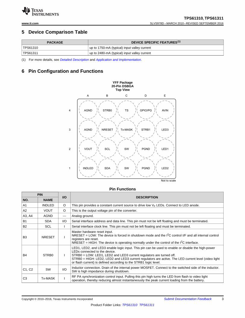
A B C D E
4
3
2
1
Not to scale
AGND STRB0 TS GPIO/PG AVIN
AGND NRESET Tx-MASK STRB1 LED3
VOUT SCL SW PGND LED1
INDLED SDA SW PGND LED2
3
TPS61310, TPS61311www.ti.com SLVS978D –MARCH 2010–REVISED SEPTEMBER 2016
Product Folder Links: TPS61310 TPS61311
Submit Documentation FeedbackCopyright © 2010–2016, Texas Instruments Incorporated
(1) For more details, see Detailed Description and Application and Implementation.
5 Device Comparison Table
PACKAGE DEVICE SPECIFIC FEATURES (1)
TPS61310 up to 1750-mA (typical) input valley currentTPS61311 up to 2480-mA (typical) input valley current
6 Pin Configuration and Functions
YFF Package20-Pin DSBGA
Top View
Pin FunctionsPIN
I/O DESCRIPTIONNO. NAMEA1 INDLED O This pin provides a constant current source to drive low VF LEDs. Connect to LED anode.A2 VOUT O This is the output voltage pin of the converter.A3, A4 AGND — Analog ground.B1 SDA I/O Serial interface address and data line. This pin must not be left floating and must be terminated.B2 SCL I Serial interface clock line. This pin must not be left floating and must be terminated.
B3 NRESET I
Master hardware reset input.NRESET = LOW: The device is forced in shutdown mode and the I2C control I/F and all internal controlregisters are reset.NRESET = HIGH: The device is operating normally under the control of the I2C interface.
B4 STRB0 I
LED1, LED2, and LED3 enable logic input. This pin can be used to enable or disable the high-powerLEDs connected to the device.STRB0 = LOW: LED1, LED2 and LED3 current regulators are turned off.STRB0 = HIGH: LED2, LED2 and LED3 current regulators are active. The LED current level (video lightor flash current) is defined according to the STRB1 logic level.
C1, C2 SW I/O Inductor connection. Drain of the internal power MOSFET. Connect to the switched side of the inductor.SW is high impedance during shutdown.
C3 Tx-MASK I RF PA synchronization control input. Pulling this pin high turns the LED from flash to video lightoperation, thereby reducing almost instantaneously the peak current loading from the battery.
4
TPS61310, TPS61311SLVS978D –MARCH 2010–REVISED SEPTEMBER 2016 www.ti.com
Product Folder Links: TPS61310 TPS61311
Submit Documentation Feedback Copyright © 2010–2016, Texas Instruments Incorporated
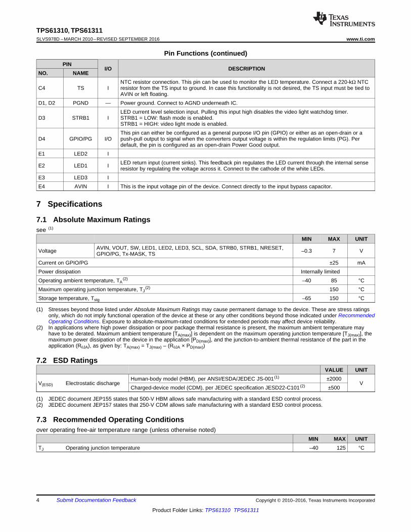
Pin Functions (continued)PIN
I/O DESCRIPTIONNO. NAME
C4 TS INTC resistor connection. This pin can be used to monitor the LED temperature. Connect a 220-kΩ NTCresistor from the TS input to ground. In case this functionality is not desired, the TS input must be tied toAVIN or left floating.
D1, D2 PGND — Power ground. Connect to AGND underneath IC.
D3 STRB1 ILED current level selection input. Pulling this input high disables the video light watchdog timer.STRB1 = LOW: flash mode is enabled.STRB1 = HIGH: video light mode is enabled.
D4 GPIO/PG I/OThis pin can either be configured as a general purpose I/O pin (GPIO) or either as an open-drain or apush-pull output to signal when the converters output voltage is within the regulation limits (PG). Perdefault, the pin is configured as an open-drain Power Good output.
E1 LED2 I
E2 LED1 I LED return input (current sinks). This feedback pin regulates the LED current through the internal senseresistor by regulating the voltage across it. Connect to the cathode of the white LEDs.
E3 LED3 IE4 AVIN I This is the input voltage pin of the device. Connect directly to the input bypass capacitor.
(1) Stresses beyond those listed under Absolute Maximum Ratings may cause permanent damage to the device. These are stress ratingsonly, which do not imply functional operation of the device at these or any other conditions beyond those indicated under RecommendedOperating Conditions. Exposure to absolute-maximum-rated conditions for extended periods may affect device reliability.
(2) In applications where high power dissipation or poor package thermal resistance is present, the maximum ambient temperature mayhave to be derated. Maximum ambient temperature [TA(max)] is dependent on the maximum operating junction temperature [TJ(max)], themaximum power dissipation of the device in the application [PD(max)], and the junction-to-ambient thermal resistance of the part in theapplication (RθJA), as given by: TA(max) = TJ(max) – (RθJA × PD(max))
7 Specifications
7.1 Absolute Maximum Ratingssee (1)
MIN MAX UNIT
Voltage AVIN, VOUT, SW, LED1, LED2, LED3, SCL, SDA, STRB0, STRB1, NRESET,GPIO/PG, Tx-MASK, TS –0.3 7 V
Current on GPIO/PG ±25 mAPower dissipation Internally limitedOperating ambient temperature, TA
(2) –40 85 °CMaximum operating junction temperature, TJ
(2) 150 °CStorage temperature, Tstg –65 150 °C
(1) JEDEC document JEP155 states that 500-V HBM allows safe manufacturing with a standard ESD control process.(2) JEDEC document JEP157 states that 250-V CDM allows safe manufacturing with a standard ESD control process.
7.2 ESD RatingsVALUE UNIT
V(ESD) Electrostatic dischargeHuman-body model (HBM), per ANSI/ESDA/JEDEC JS-001 (1) ±2000
VCharged-device model (CDM), per JEDEC specification JESD22-C101 (2) ±500
7.3 Recommended Operating Conditionsover operating free-air temperature range (unless otherwise noted)
MIN MAX UNITTJ Operating junction temperature –40 125 °C
5
TPS61310, TPS61311www.ti.com SLVS978D –MARCH 2010–REVISED SEPTEMBER 2016
Product Folder Links: TPS61310 TPS61311
Submit Documentation FeedbackCopyright © 2010–2016, Texas Instruments Incorporated
(1) For more information about traditional and new thermal metrics, see the Semiconductor and IC Package Thermal Metrics applicationreport.
7.4 Thermal Information
THERMAL METRIC (1)TPS6131x
UNITYFF (DSBGA)20 PINS
RθJA Junction-to-ambient thermal resistance 71 °C/WRθJC(top) Junction-to-case (top) thermal resistance 0.4 °C/WRθJB Junction-to-board thermal resistance 21 °C/WψJT Junction-to-top characterization parameter 1.9 °C/WψJB Junction-to-board characterization parameter 11.2 °C/W
(1) Verified by characterization. Not tested in production.(2) Verified by characterization. Not tested in production.
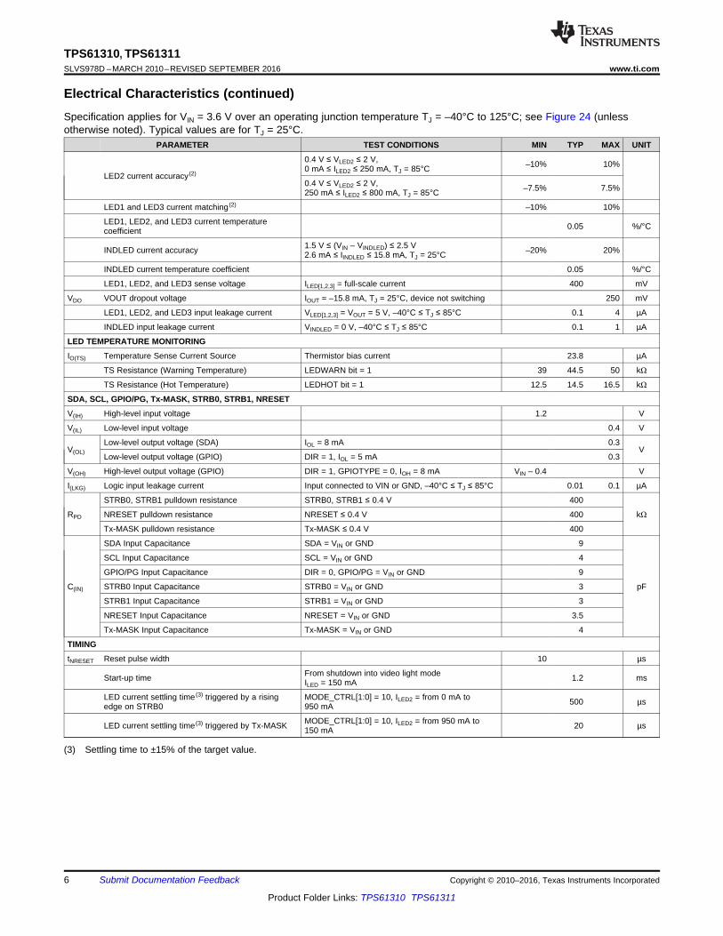
7.5 Electrical CharacteristicsSpecification applies for VIN = 3.6 V over an operating junction temperature TJ = –40°C to 125°C; see Figure 24 (unlessotherwise noted). Typical values are for TJ = 25°C.
PARAMETER TEST CONDITIONS MIN TYP MAX UNIT
SUPPLY CURRENT
VIN Input voltage 2.5 5.5 V
IQ Operating quiescent current into AVIN
IOUT = 0 mA, device not switching (Power SafeMode), –40°C ≤ TJ ≤ 85°C 590 700 µA
IOUT(DC) = 0 mA, PWM operation VOUT = 4.95 V,voltage regulation mode 11.3 mA
ISD Shutdown current –40°C ≤ TJ ≤ 85°C 1 5 µA
VUVLOUndervoltage lockout threshold(analog circuitry) VIN falling 2.3 2.4 V
OUTPUT
VOUT
Output voltageCurrent regulation mode VIN 5.5
VVoltage regulation mode 3.825 5.7
Internal feedback voltage accuracy 2.5 V ≤ VIN ≤ 4.8 V, –20°C ≤ TJ ≤ 125°C, Boostmode, PWM voltage regulation –2% 2%
Power-save mode ripple voltage IOUT = 10 mA 0.015 × VOUT VP–P
OVPOutput overvoltage protection
VOUT rising, 0000 ≤ OV[3:0] ≤ 0100 4.5 4.65 4.8
VVOUT rising, 0101 ≤ OV[3:0] ≤ 1111 5.8 6 6.2
Output overvoltage protection hysteresis VOUT falling 0.15
POWER SWITCH
rDS(on) Switch MOSFET ON-resistance VOUT = VGS = 3.6 V 90 mΩ
Rectifier MOSFET ON-resistance VOUT = VGS = 3.6 V 135 mΩ
Ilkg(SW) Leakage into SW VOUT = 0 V, SW = 3.6 V, –40°C ≤ TJ ≤ 85°C 0.3 4 µA
Ilim Rectifier valley current limit (open loop) VOUT = 4.95 V, –20°C ≤ TJ ≤ 85°C,PWM operation, relative to selected ILIM –15% 15%
OSCILLATOR
fOSC Oscillator frequency 1.92 MHz
fACC Oscillator frequency –10% 7%
THERMAL SHUTDOWN, HOT DIE DETECTOR
Thermal shutdown (1) 140 160 °C
Thermal shutdown hysteresis (1) 20 °C
Hot die detector accuracy (1) –8 8 °C
LED CURRENT REGULATOR
LED1 and LED3 current accuracy (2)
0.4 V ≤ VLED[1,3] ≤ 2 V,0 mA ≤ ILED[1,3] ≤ 100 mA, TJ = 85°C –10% 10%
0.4 V ≤ VLED[1,3] ≤ 2 V,100 mA < ILED[1,3] ≤ 400 mA, TJ = 85°C –7.5% 7.5%
6
TPS61310, TPS61311SLVS978D –MARCH 2010–REVISED SEPTEMBER 2016 www.ti.com
Product Folder Links: TPS61310 TPS61311
Submit Documentation Feedback Copyright © 2010–2016, Texas Instruments Incorporated
Electrical Characteristics (continued)Specification applies for VIN = 3.6 V over an operating junction temperature TJ = –40°C to 125°C; see Figure 24 (unlessotherwise noted). Typical values are for TJ = 25°C.
PARAMETER TEST CONDITIONS MIN TYP MAX UNIT
(3) Settling time to ±15% of the target value.
LED2 current accuracy (2)
0.4 V ≤ VLED2 ≤ 2 V,0 mA ≤ ILED2 ≤ 250 mA, TJ = 85°C –10% 10%
0.4 V ≤ VLED2 ≤ 2 V,250 mA ≤ ILED2 ≤ 800 mA, TJ = 85°C –7.5% 7.5%
LED1 and LED3 current matching (2) –10% 10%
LED1, LED2, and LED3 current temperaturecoefficient 0.05 %/°C
INDLED current accuracy 1.5 V ≤ (VIN – VINDLED) ≤ 2.5 V2.6 mA ≤ IINDLED ≤ 15.8 mA, TJ = 25°C –20% 20%
INDLED current temperature coefficient 0.05 %/°C
LED1, LED2, and LED3 sense voltage ILED[1,2,3] = full-scale current 400 mV
VDO VOUT dropout voltage IOUT = –15.8 mA, TJ = 25°C, device not switching 250 mV
LED1, LED2, and LED3 input leakage current VLED[1,2,3] = VOUT = 5 V, –40°C ≤ TJ ≤ 85°C 0.1 4 µA
INDLED input leakage current VINDLED = 0 V, –40°C ≤ TJ ≤ 85°C 0.1 1 µA
LED TEMPERATURE MONITORING
IO(TS) Temperature Sense Current Source Thermistor bias current 23.8 µA
TS Resistance (Warning Temperature) LEDWARN bit = 1 39 44.5 50 kΩ
TS Resistance (Hot Temperature) LEDHOT bit = 1 12.5 14.5 16.5 kΩ
SDA, SCL, GPIO/PG, Tx-MASK, STRB0, STRB1, NRESET
V(IH) High-level input voltage 1.2 V
V(IL) Low-level input voltage 0.4 V
V(OL)Low-level output voltage (SDA) IOL = 8 mA 0.3
VLow-level output voltage (GPIO) DIR = 1, IOL = 5 mA 0.3
V(OH) High-level output voltage (GPIO) DIR = 1, GPIOTYPE = 0, IOH = 8 mA VIN – 0.4 V
I(LKG) Logic input leakage current Input connected to VIN or GND, –40°C ≤ TJ ≤ 85°C 0.01 0.1 µA
RPD
STRB0, STRB1 pulldown resistance STRB0, STRB1 ≤ 0.4 V 400
kΩNRESET pulldown resistance NRESET ≤ 0.4 V 400
Tx-MASK pulldown resistance Tx-MASK ≤ 0.4 V 400
C(IN)
SDA Input Capacitance SDA = VIN or GND 9
pF
SCL Input Capacitance SCL = VIN or GND 4
GPIO/PG Input Capacitance DIR = 0, GPIO/PG = VIN or GND 9
STRB0 Input Capacitance STRB0 = VIN or GND 3
STRB1 Input Capacitance STRB1 = VIN or GND 3
NRESET Input Capacitance NRESET = VIN or GND 3.5
Tx-MASK Input Capacitance Tx-MASK = VIN or GND 4
TIMING
tNRESET Reset pulse width 10 µs
Start-up time From shutdown into video light modeILED = 150 mA 1.2 ms
LED current settling time (3) triggered by a risingedge on STRB0
MODE_CTRL[1:0] = 10, ILED2 = from 0 mA to950 mA 500 µs
LED current settling time (3) triggered by Tx-MASK MODE_CTRL[1:0] = 10, ILED2 = from 950 mA to150 mA 20 µs

7
TPS61310, TPS61311www.ti.com SLVS978D –MARCH 2010–REVISED SEPTEMBER 2016
Product Folder Links: TPS61310 TPS61311
Submit Documentation FeedbackCopyright © 2010–2016, Texas Instruments Incorporated
(1) Specified by design. Not tested in production.
7.6 I2C Interface Timing Requirementssee (1)
MIN MAX UNIT
f(SCL) SCL Clock Frequency
Standard mode 100kHz
Fast mode 400High-speed mode (write operation), CB – 100 pF max 3.4
MHzHigh-speed mode (read operation), CB – 100 pF max 3.4High-speed mode (write operation), CB – 400 pF max 1.7High-speed mode (read operation), CB – 400 pF max 1.7
tBUFBus Free Time Between a STOPand START Condition
Standard mode 4.7µs
Fast mode 1.3
tHD, tSTAHold Time (Repeated) STARTCondition
Standard mode 4 µsFast mode 600
nsHigh-speed mode 160
tLOW LOW Period of the SCL Clock
Standard mode 4.7µs
Fast mode 1.3High-speed mode, CB – 100 pF max 160
nsHigh-speed mode, CB – 400 pF max 320
tHIGH HIGH Period of the SCL Clock
Standard mode 4 µsFast mode 600
nsHigh-speed mode, CB – 100 pF max 60High-speed mode, CB – 400 pF max 120
tSU, tSTASetup Time for a Repeated STARTCondition
Standard mode 4.7 µsFast mode 600
nsHigh-speed mode 160
tSU, tDAT Data Setup TimeStandard mode 250
nsFast mode 100High-speed mode 10
tHD, tDAT Data Hold Time
Standard mode 0 3.45µs
Fast mode 0 0.9High-speed mode, CB – 100 pF max 0 70
nsHigh-speed mode, CB – 400 pF max 0 150
tRCL Rise Time of SCL Signal
Standard mode 20 + 0.1 × CB 1000
nsFast mode 20 + 0.1 × CB 300High-speed mode, CB – 100 pF max 10 40High-speed mode, CB – 400 pF max 20 80
tRCL1
Rise Time of SCL Signal After aRepeated START Condition andAfter an Acknowledge BIT
Standard mode 20 + 0.1 × CB 1000
nsFast mode 20 + 0.1 × CB 300High-speed mode, CB – 100 pF max 10 80High-speed mode, CB – 400 pF max 20 160
tFCL Fall Time of SCL Signal
Standard mode 20 + 0.1 × CB 300
nsFast mode 20 + 0.1 × CB 300High-speed mode, CB – 100 pF max 10 40High-speed mode, CB – 400 pF max 20 80
tRDA Rise Time of SDA Signal
Standard mode 20 + 0.1 × CB 1000
nsFast mode 20 + 0.1 × CB 300High-speed mode, CB – 100 pF max 10 80High-speed mode, CB – 400 pF max 20 160

Sr PSr
tfDA trDA
thd;DAT
tsu;STA thd;STA tsu;DAT
tsu;STO
trCL1
tfCL
tHIGH tLOW tLOW tHIGH
trCLtrCL1
= MCS Current Source Pull-Up
= R(P) Resistor Pull-Up
SDAH
SCLH
Note A: First rising edge of the SCLH signal after Sr and after each acknowledge bit.
See Note ASee Note A
tf tLOWtr
thd;STA
thd;DAT
tsu;DATtf
HIGH
tsu;STA
S Sr P S
thd;STAtr
tBUF
tsu;STO
SDA
SCL
8
TPS61310, TPS61311SLVS978D –MARCH 2010–REVISED SEPTEMBER 2016 www.ti.com
Product Folder Links: TPS61310 TPS61311
Submit Documentation Feedback Copyright © 2010–2016, Texas Instruments Incorporated
I2C Interface Timing Requirements (continued)see (1)
MIN MAX UNIT
tFDA Fall Time of SDA Signal
Standard mode 20 + 0.1 × CB 300
nsFast mode 20 + 0.1 × CB 300High-speed mode, CB – 100 pF max 10 80High-speed mode, CB – 400 pF max 20 160
tSU, tSTO Setup Time for STOP ConditionStandard mode 4 µsFast mode 600
nsHigh-speed mode 160
CB Capacitive Load for SDA and SCL 400 pF
(1) Maximum power dissipation is a function of TJ(max), RθJA and TA. The maximum allowable power dissipation at any allowable ambienttemperature is PD = (TJ(max) – TA) / RθJA.
7.7 Dissipation RatingsPACKAGE POWER RATING (TA = 25°C) DERATING FACTOR ABOVE TA = 25°C (1)
YFF 1.4 W 14 mW/°C
Figure 1. Serial Interface Timing For F/S-Mode
Figure 2. Serial Interface Timing For H/S-Mode

0
100
200
300
400
500
600
700
800
900
400 500 600 700 800 900 1000 1100 1200 1300 1400
LED2 Pin Headroom Voltage - mV
ILED2 = 800 mA
ILED2 = 700 mA
ILED2 = 550 mA
ILED2 = 300 mA
ILED2 = 450 mA
ILED2 = 350 mA
I = 1750 mALIM
LE
D2 C
urr
en
t -
mA
0
250
500
750
1000
1250
1500
1750
2000
2.5 2.9 3.3 3.7 4.1 4.5 4.9 5.3
V - Input Voltage - VI
I = 1750 mA,
Tx-MASK = LowLIM
ILED1 = 50 mAILED2 = 550 mA
ILED3 = 2
ILED1 = 50 mAILED2 = 600 mA
ILED3 = 3
ILED1 = 50 mAILED2 = 450 mA
ILED3 = 2
ILED1 = 50 mAILED2 = 275 mA
ILED3 = 2
DC
In
pu
t C
urr
en
t -
mA
0
10
20
30
40
50
60
70
80
90
100
LE
D P
ow
er
Eff
icie
ncy (
PL
ED
/PIN
) -
%
2.5 2.9 3.3 3.7 4.1 4.5 4.9 5.3
V - Input Voltage - VI
ILED1 = 50 mAILED2 = 100 mA
ILED3 =
I = 1750 mA,
Tx-MASK = LowLIM
ILED1 = 0 mAILED2 = 200 mA
ILED3 = 10
ILED1 = 5 mAILED2 = 150 mA
ILED3 = 7
ILED1 = 50 mAILED2 = 550 mA
ILED3 = 2
ILED1 = 50 mAILED2 = 600 mA
ILED3 = 3
ILED1 = 50 mAILED2 = 450 mA
ILED3 = 2
2.5 2.9 3.3 3.7 4.1 4.5 4.9 5.3
V - Input Voltage - VI
0
10
20
30
40
50
60
70
80
90
100
LE
D P
ow
er
Eff
icie
ncy (
PL
ED
/PIN
) -
%
ILED2 = 75 mA
ILED2 = 100 mA
ILED2 = 150 mA
ILED2 = 225 mA
I = 1750 mA,
Tx-MASK = LowLED2 Channel
LIM
9
TPS61310, TPS61311www.ti.com SLVS978D –MARCH 2010–REVISED SEPTEMBER 2016
Product Folder Links: TPS61310 TPS61311
Submit Documentation FeedbackCopyright © 2010–2016, Texas Instruments Incorporated
7.8 Typical CharacteristicsTable 1. Table of Graphs
CAPTION FIGURELED Power Efficiency Input Voltage Figure 3, Figure 4DC Input Current Input Voltage Figure 5LED Current LED Pin Headroom Voltage Figure 6, Figure 7LED Current LED Current Digital Code Figure 8, Figure 9, Figure 10, Figure 11INDLED Current INDLED Pin Headroom Voltage Figure 12Efficiency Output Current Figure 13, Figure 14DC Output Voltage Load Current Figure 15, Figure 16Maximum Output Current Input Voltage Figure 17DC Precharge Current Differential I/O Voltage Figure 18, Figure 19Supply Current Input Voltage Figure 20Temperature Detection Threshold Figure 21, Figure 22Junction Temperature Port Voltage Figure 23
Figure 3. LED Power Efficiency vs Input Voltage Figure 4. LED Power Efficiency vs Input Voltage
Figure 5. DC Input Current vs Input Voltage Figure 6. LED2 Current vs LED2 Pin Headroom Voltage

200
225
250
275
300
325
350
375
400
425
450
200 225 250 275 300 325 350 375 400 425 450
LED1, LED3 Current Digital Code - mA
V = 4.5 VINV = 3.6 VIN
V = 2.5 VIN
I = 1750 mALIM
LE
D1, L
ED
3 C
urr
en
t -
mA
0
1
2
3
4
5
6
7
8
9
0.5 0.7 0.9 1.1 1.3 1.5 1.7 1.9
INDLED Pin Headroom Voltage - V
IND
LE
D C
urr
en
t -
mA
INDLED = 0011
INDLED = 0010
INDLED = 0001
T = 85°CA
T = 25°CAT = -40°CA
T = 85°CA
T = 25°CA
T = -40°CAT = 85°CA
T = 25°CA
V = 3.6 VIN
T = -40°CA
25
50
75
100
125
25 50 75 100 125
LED1, LED3 Current Digital Code - mA
V = 4.5 VIN
V = 3.6 VIN
V = 2.5 VIN
LE
D1
, L
ED
3 C
urr
en
t -
mA
I = 1750 mALIM
200
250
300
350
400
450
500
550
600
650
700
750
800
850
900
LED2 Current Digital Code - mA
V = 4.5 VINV = 3.6 VIN
I = 1750 mALIM
200 300 400 500 600 700 800 900
V = 2.5 VIN
LE
D2
Cu
rre
nt
- m
A
0
25
50
75
100
125
150
175
200
225
250
275
300
0 25 50 75 100 125 150 175 200 225 250 275 300
LED2 Current Digital Code - mA
V = 2.5 VIN
V = 4.5 VIN
V = 3.6 VIN
LE
D2
Cu
rre
nt
- m
A
I = 1750 mALIM
0
100
200
300
400
500
600
700
800
900
400 500 600 700 800 900 1000 1100 1200 1300 1400
LED1, LED3 Pin Headroom Voltage - mV
LE
D1 +
LE
D3 C
urr
en
t -
mA
ILED1 = ILED3 = 400 mA
I = 1750 mALIM
ILED1 = ILED3 = 350 mA
ILED1 = ILED3 = 300 mA
ILED1 = ILED3 = 250 mA
10
TPS61310, TPS61311SLVS978D –MARCH 2010–REVISED SEPTEMBER 2016 www.ti.com
Product Folder Links: TPS61310 TPS61311
Submit Documentation Feedback Copyright © 2010–2016, Texas Instruments Incorporated
Typical Characteristics (continued)
Figure 7. LED1 + LED3 Current vsLED1 + LED3 Pin Headroom Voltage
Figure 8. LED2 Current vs LED2 Current Digital Code
Figure 9. LED1, LED3 Current vsLED1, LED3 Current Digital Code
Figure 10. LED2 Current vs LED2 Current Digital Code
Figure 11. LED1, LED3 Current vsLED1, LED3 Current Digital Code
Figure 12. INDLED Current vsINDLED Pin Headroom Voltage

0
100
200
300
400
500
600
700
800
900
1000
1100
1200
1300
1400
1500
2.5 2.9 3.3 3.7 4.1 4.5 4.9 5.3
V - Input Voltage - VI
I-
Ou
tpu
t C
urr
en
t (m
ax)
- m
AO
V = 4.95 V,
I = 1250 mAOUT
LIM
Voltage Mode Regulation
V = 5.7 V,
I = 1250 mAOUT
LIM
0
50
100
150
200
250
300
350
400
0 0.6 1.2 1.8 2.4 3 3.6 4.2Differential Input - Output Voltage - V
V = 3.6 V, T = 25°CIN A
V = 2.5 V, T = 25°CIN A
V = 4.2 V, T = 25°CIN A
DC
Pre
-Ch
arg
e C
urr
en
t -
mA
4.8
4.85
4.9
4.95
5
5.05
5.1
5.15
5.2
1 10 100 1000 10000
I - Output Current - mAO
V-
Ou
tpu
t V
olt
ag
e (
DC
) -
VO
Voltage Mode Regulation
Forced PWM Operation
PFM/PWM Operation
V = 3.6 VIN
V = 2.5 VIN
V = 4.95 V,
I = 1750 mAOUT
LIM
V = 4.2 VIN
3.71
3.749
3.787
3.825
3.863
3.902
3.94
3.978
4.016
2.5 2.9 3.3 3.7 4.1 4.5 4.9 5.3I - Output Current - mAO
V-
Ou
tpu
t V
olt
ag
e (
DC
) -
VO
I = 0 mAOUT
I = 100 mAOUT
I = 1000 mAOUT
Voltage Mode Regulation
V = 3.825 VOUT
I = 1750 mALIM
0
10
20
30
40
50
60
70
80
90
100
1 10 100 1000 10000
I - Output Current - mAO
Eff
icie
ncy -
%
Forced PWM Operation
PFM/PWM Operation
V = 4.2 VIN
V = 3.6 VIN
V = 2.5 VINV = 3 VIN
V = 3.825 V
Voltage Mode Regulation
OUT
I = 1750 mALIM
0
10
20
30
40
50
60
70
80
90
100
1 10 100 1000 10000
I - Output Current - mAO
Eff
icie
ncy -
%
V = 4.2 VIN
V = 3.6 VINV = 2.5 VIN
V = 4.95 V
Voltage Mode Regulation
OUT
I = 1750 mALIM
V = 3 VIN
PFM/PWM Operation
Forced PWM Operation
11
TPS61310, TPS61311www.ti.com SLVS978D –MARCH 2010–REVISED SEPTEMBER 2016
Product Folder Links: TPS61310 TPS61311
Submit Documentation FeedbackCopyright © 2010–2016, Texas Instruments Incorporated
Typical Characteristics (continued)
Figure 13. Efficiency vs Output Current Figure 14. Efficiency vs Output Current
Figure 15. DC Output Voltage vs Load Current Figure 16. DC Output Voltage vs Load Current
Figure 17. Maximum Output Current vs Input Voltage Figure 18. DC Precharge Current vsDifferential I/O Voltage
-50
-25
0
25
50
75
100
125
150
175
200
-0.6 -0.55 -0.5 -0.45 -0.4 -0.35 -0.3 -0.25 -0.2 -0.15 -0.1
Port Voltage - V
T-
Ju
nc
tio
n T
em
pe
ratu
re -
°C
J
VP
OR
T
PortInput Buffer
100 Am
I = -100 APORT m
STRB1 Input
Tx-MASK Input
0
2
4
6
8
10
12
14
16
18
20
22
24
26
28
64 65 66 67 68 69 70 71 72 73 74 75Temperature Detection (70°C Threshold)
Sam
ple
Perc
en
tag
e -
%
V = 3.6 VIN
Sample Size = 76
0
2
4
6
8
10
12
14
16
18
20
22
24
26
50 51 52 53 54 55 56 57 58 59 60Temperature Detection (55°C Threshold)
Sam
ple
Perc
en
tag
e -
%
V = 3.6 VIN
Sample Size = 76
0
50
100
150
200
250
300
350
400
0 0.6 1.2 1.8 2.4 3 3.6 4.2
Differential Input - Output Voltage - V
V = 3.6 V, T = -40°CIN A
V = 3.6 V, T = 25°CIN A
V = 3.6 V, T = 85°CIN A
DC
Pre
-Ch
arg
e C
urr
en
t -
mA
1000
500
600
700
800
900
1100
1200
1300
1400
1500
2.5 2.9 3.3 3.7 4.1 4.5 4.9 5.3V - Input Voltage - VI
I-
Su
pp
ly C
urr
en
t -
AC
Cm
V = 5.7 V, T = 25°COUT A
V = 3.825 V,
T = 25°COUT
AV = 4.95 V,
T = 25°COUT
A
V = 4.95 V, T = 85°COUT A
V = 4.95 V,
T = -40°COUT
A
I = 0 mA
ENPSM bit = ENVM bit = 1OUT
12
TPS61310, TPS61311SLVS978D –MARCH 2010–REVISED SEPTEMBER 2016 www.ti.com
Product Folder Links: TPS61310 TPS61311
Submit Documentation Feedback Copyright © 2010–2016, Texas Instruments Incorporated
Typical Characteristics (continued)
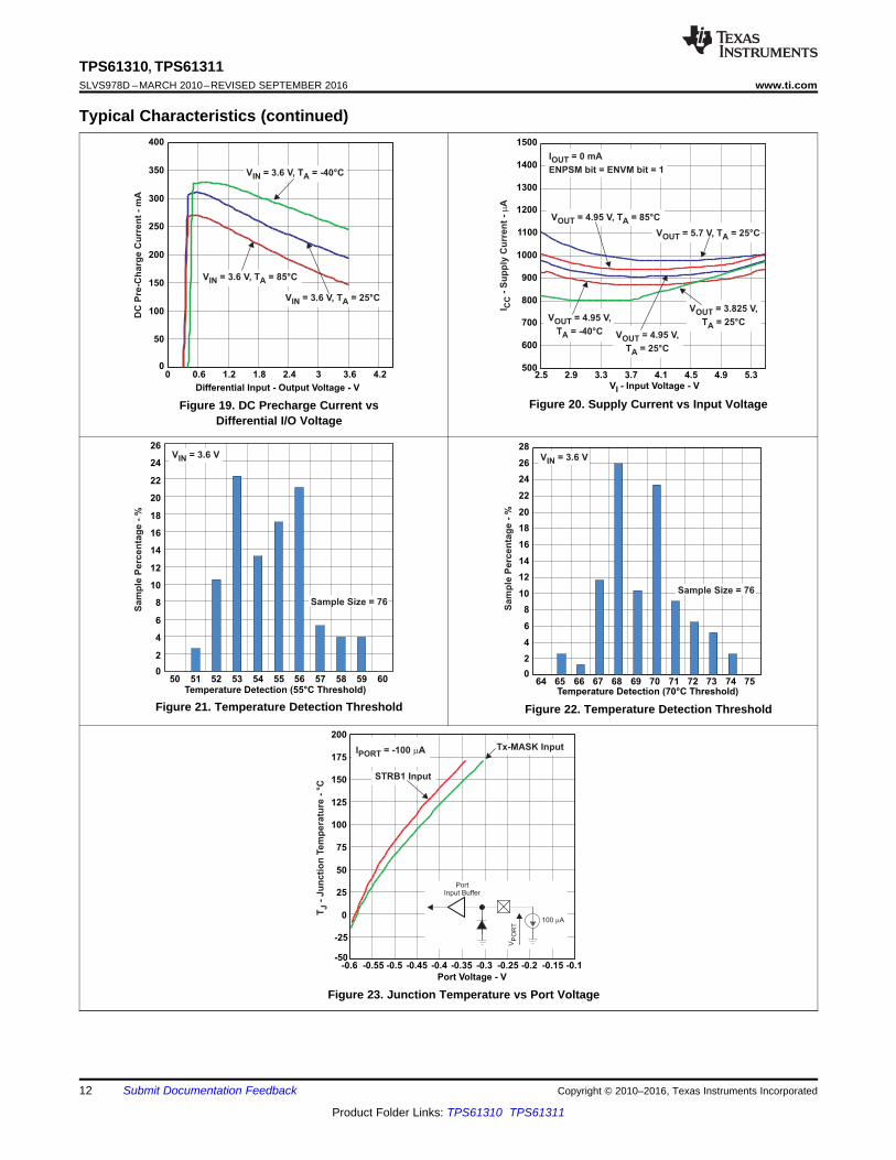
Figure 19. DC Precharge Current vsDifferential I/O Voltage
Figure 20. Supply Current vs Input Voltage
Figure 21. Temperature Detection Threshold Figure 22. Temperature Detection Threshold
Figure 23. Junction Temperature vs Port Voltage
VOUT
AVIN
SW
CI
SW
LED 1
PGND
PGND
AGND
L
2 .2 mH
SDA
SCLI2C I /F
TPS61310
LED 2
LED 3
D 1 D 22 .5 V .. 5 .5 V
STRB0
TS
NRESET
GPIO /PG
INDLED
PrivacyIndicator
NTC
Tx -MASK
STRB1
CO
10 mF4.7 mF
AGND
Copyright © 2016, Texas Instruments Incorporated
13
TPS61310, TPS61311www.ti.com SLVS978D –MARCH 2010–REVISED SEPTEMBER 2016
Product Folder Links: TPS61310 TPS61311
Submit Documentation FeedbackCopyright © 2010–2016, Texas Instruments Incorporated
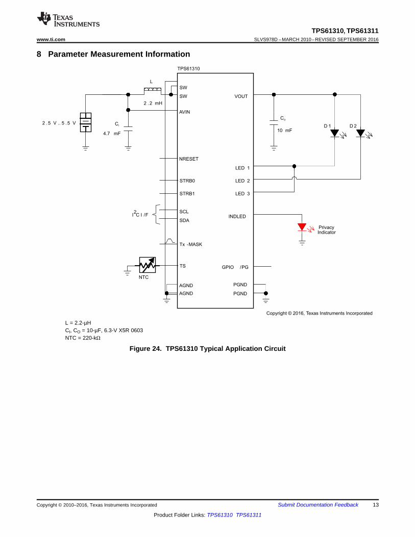
8 Parameter Measurement Information
L = 2.2-µHCI, CO = 10-µF, 6.3-V X5R 0603NTC = 220-kΩ
Figure 24. TPS61310 Typical Application Circuit
14
TPS61310, TPS61311SLVS978D –MARCH 2010–REVISED SEPTEMBER 2016 www.ti.com
Product Folder Links: TPS61310 TPS61311
Submit Documentation Feedback Copyright © 2010–2016, Texas Instruments Incorporated
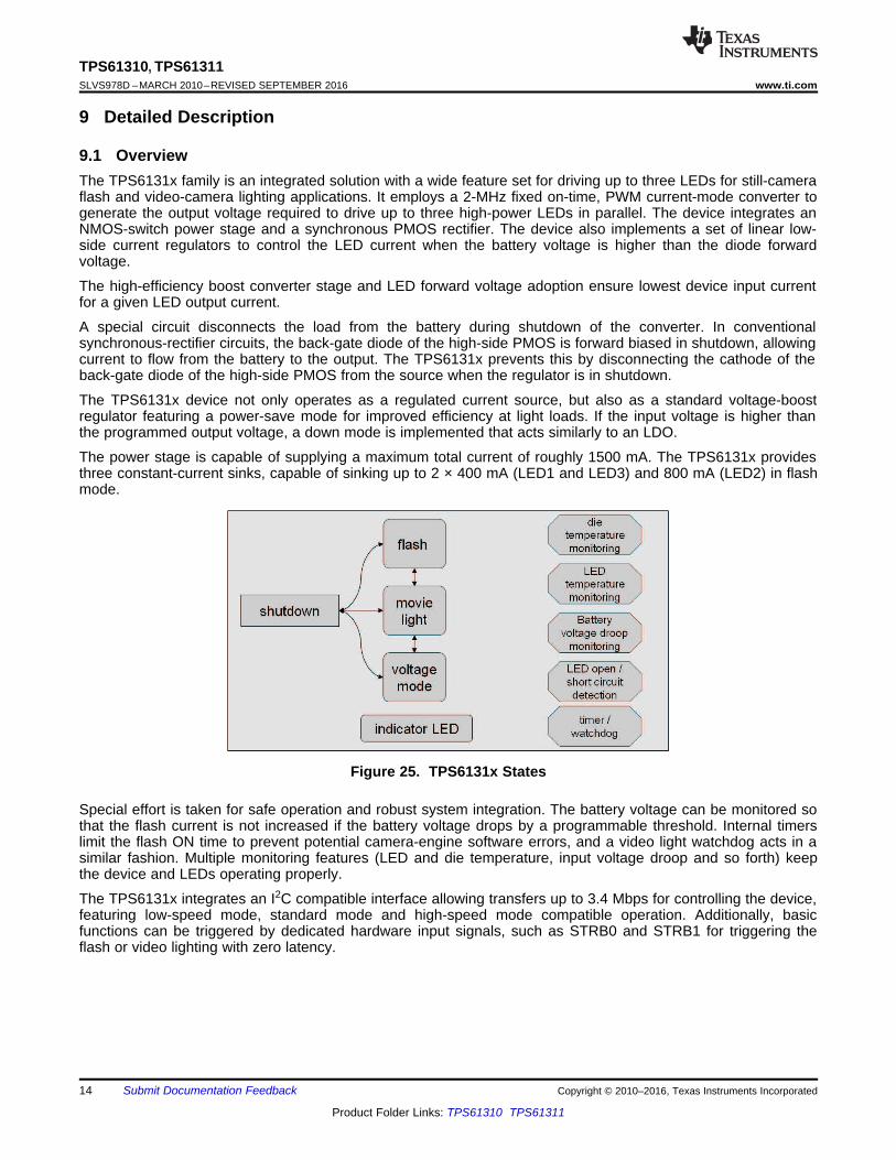
9 Detailed Description
9.1 OverviewThe TPS6131x family is an integrated solution with a wide feature set for driving up to three LEDs for still-cameraflash and video-camera lighting applications. It employs a 2-MHz fixed on-time, PWM current-mode converter togenerate the output voltage required to drive up to three high-power LEDs in parallel. The device integrates anNMOS-switch power stage and a synchronous PMOS rectifier. The device also implements a set of linear low-side current regulators to control the LED current when the battery voltage is higher than the diode forwardvoltage.
The high-efficiency boost converter stage and LED forward voltage adoption ensure lowest device input currentfor a given LED output current.
A special circuit disconnects the load from the battery during shutdown of the converter. In conventionalsynchronous-rectifier circuits, the back-gate diode of the high-side PMOS is forward biased in shutdown, allowingcurrent to flow from the battery to the output. The TPS6131x prevents this by disconnecting the cathode of theback-gate diode of the high-side PMOS from the source when the regulator is in shutdown.
The TPS6131x device not only operates as a regulated current source, but also as a standard voltage-boostregulator featuring a power-save mode for improved efficiency at light loads. If the input voltage is higher thanthe programmed output voltage, a down mode is implemented that acts similarly to an LDO.
The power stage is capable of supplying a maximum total current of roughly 1500 mA. The TPS6131x providesthree constant-current sinks, capable of sinking up to 2 × 400 mA (LED1 and LED3) and 800 mA (LED2) in flashmode.
Figure 25. TPS6131x States
Special effort is taken for safe operation and robust system integration. The battery voltage can be monitored sothat the flash current is not increased if the battery voltage drops by a programmable threshold. Internal timerslimit the flash ON time to prevent potential camera-engine software errors, and a video light watchdog acts in asimilar fashion. Multiple monitoring features (LED and die temperature, input voltage droop and so forth) keepthe device and LEDs operating properly.
The TPS6131x integrates an I2C compatible interface allowing transfers up to 3.4 Mbps for controlling the device,featuring low-speed mode, standard mode and high-speed mode compatible operation. Additionally, basicfunctions can be triggered by dedicated hardware input signals, such as STRB0 and STRB1 for triggering theflash or video lighting with zero latency.

AVIN
VOUT
SW
LED2
REF
SCL
SDAI2C I/F
AGND PGND
STRB1
CURRENT
CONTROL
P
P
SENSE FB
COMPARATOR
ERROR
AMPLIFIER
OVP
COMPARATOR
VOLTAGE
REGULATIONCURRENT
REGULATION
VREF
ON/OFF
Control
Logic
Max tON Timer
DAC
TON
Control
Backgate
Control
LED1
CURRENT
CONTROL
Low-Side LED Current Regulator
P
SENSE FB
ON/OFF
P
LED3
VLED Sense
DAC
SENSE FB
STRB0
Tx-MASK
INDLED
AVIN
INDC[1:0]
High-Side LED Current Regulator
Slew-Rate
Controller
NRESET
LED Current Ramp
R
S
Q
Q
CONTROL LOGIC
TS
AVIN
23µA
VREF = 1.05V
VREF = 0.345V
WARNING
HOT
Undervoltage
Lockout
Bias Supply
Bandgap
Hot Die
Indicator
VREF = 1.238V
350 kΩ
BATTERY DROOP
THRESHOLD
Digital
Filter
VBAT DROOP
COMPARATOR
Oscillator
(STOP)
Copyright © 2016, Texas Instruments Incorporated
15
TPS61310, TPS61311www.ti.com SLVS978D –MARCH 2010–REVISED SEPTEMBER 2016
Product Folder Links: TPS61310 TPS61311
Submit Documentation FeedbackCopyright © 2010–2016, Texas Instruments Incorporated
9.2 Functional Block Diagram
Figure 26. TPS6131x

16-bit Prescaler Safety Timer
Time-Out (TO)
Dimming
(DIM)
Timer
Value
(STIM)
STRB0
tPULSE
CLOCK
Edge Detect
Start
MODE 0
CURRENT REGULATOR MODE – DC LIGHT / FLASH ACTIVE
MODE 0 = LOW
MODE 1 = HIGH
Duty-Cycle Generator (5% ... 67%)LED1-3 ON/OFF CONTROL
0: LED1-3 OFF
1: DC LIGHT CURRENT LEVEL
Start
Flash/Timer
(SFT)
Tx-MASK
0: DC LIGHT CURRENT LEVEL1: FLASH CURRENT LEVEL
LED1-3 CURRENT CONTROL
350 kW
Safety Timer Trigger
(STT)
1
0
1
GPIO/PG
(GPIO Bit)
Port Direction
(DIR)
(GPIO Bit)
PWROK
Port Type
(PG)
DC Light
Safety Timer
(11.2s)
MODE 1
MODE 0
0: NORMAL OPERATION
1: DISABLE CURRENT SINK
350 kW
STRB1MODE 1
Copyright © 2016, Texas Instruments Incorporated
16
TPS61310, TPS61311SLVS978D –MARCH 2010–REVISED SEPTEMBER 2016 www.ti.com
Product Folder Links: TPS61310 TPS61311
Submit Documentation Feedback Copyright © 2010–2016, Texas Instruments Incorporated
Functional Block Diagram (continued)
Figure 27. Timer Block
9.3 Feature Description
9.3.1 Privacy IndicatorThe privacy indicator functionality can be used to indicate when a person is being photographed or filmed. TheTPS6131x device offers two options of privacy indication: A dedicated pin driving an additional privacy indicatorLED or using the white LEDs with pulse width modulation.
9.3.1.1 Dedicated LED Privacy IndicatorThe TPS6131x device provides a high-side linear constant current source to drive low VF LEDs. The LED currentis directly regulated off the battery and can be controlled through the INDC[3:0] bits, from 2.6 mA to 15.8 mA in 7programable current steps.
The device can drive two possible hardware configurations shown in Figure 28 and Figure 29. In Figure 28 theTPS6131x device drives a privacy indicator LED towards ground.
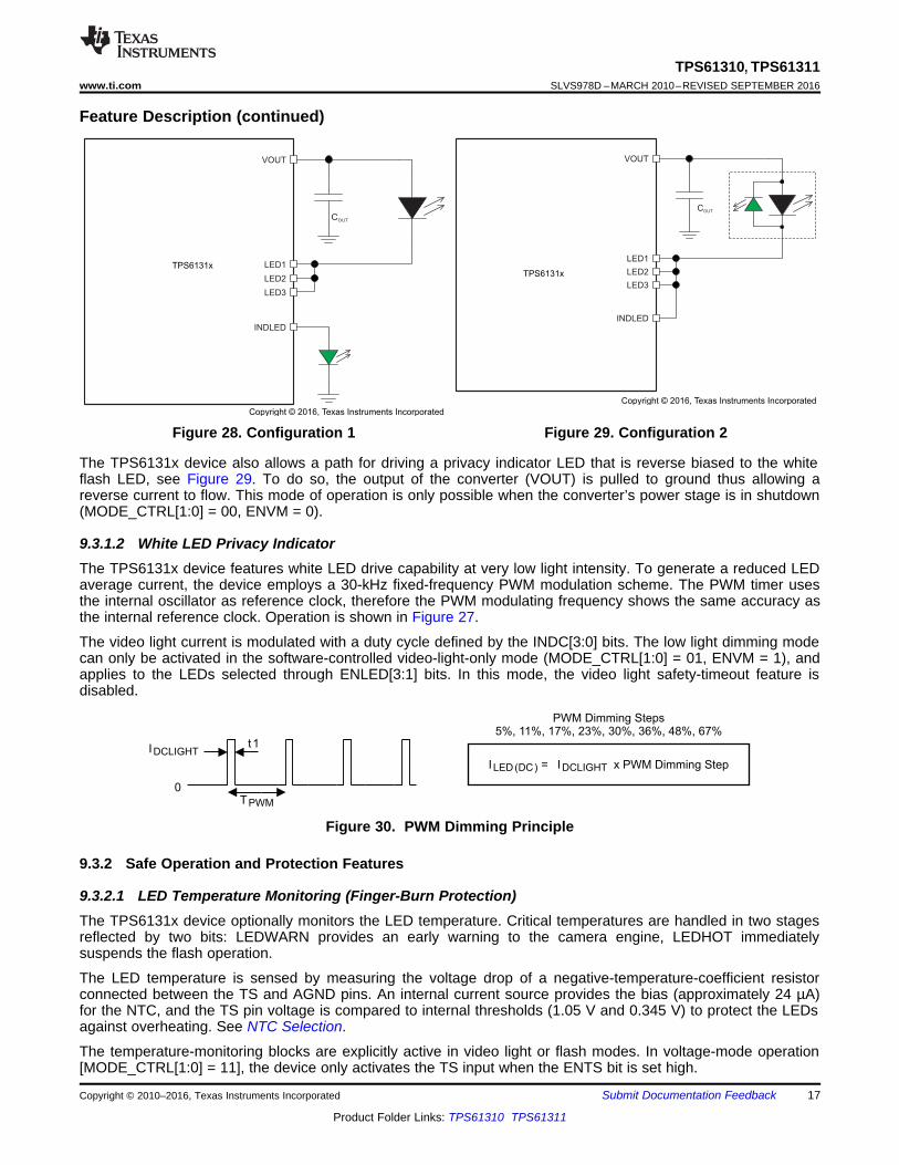
PWM Dimming Steps5%, 11%, 17%, 23%, 30%, 36%, 48%, 67%
IDCLIGHT
0
ILED (DC) = IDCLIGHT x PWM Dimming Step
t1
TPWM
TPS6131x
VOUT
COUT
INDLED
LED1
LED2
LED3
Copyright © 2016, Texas Instruments Incorporated
TPS6131x
VOUT
INDLED
LED1
LED2
LED3
COUT
Copyright © 2016, Texas Instruments Incorporated
17
TPS61310, TPS61311www.ti.com SLVS978D –MARCH 2010–REVISED SEPTEMBER 2016
Product Folder Links: TPS61310 TPS61311
Submit Documentation FeedbackCopyright © 2010–2016, Texas Instruments Incorporated
Feature Description (continued)
Figure 28. Configuration 1 Figure 29. Configuration 2
The TPS6131x device also allows a path for driving a privacy indicator LED that is reverse biased to the whiteflash LED, see Figure 29. To do so, the output of the converter (VOUT) is pulled to ground thus allowing areverse current to flow. This mode of operation is only possible when the converter’s power stage is in shutdown(MODE_CTRL[1:0] = 00, ENVM = 0).
9.3.1.2 White LED Privacy IndicatorThe TPS6131x device features white LED drive capability at very low light intensity. To generate a reduced LEDaverage current, the device employs a 30-kHz fixed-frequency PWM modulation scheme. The PWM timer usesthe internal oscillator as reference clock, therefore the PWM modulating frequency shows the same accuracy asthe internal reference clock. Operation is shown in Figure 27.
The video light current is modulated with a duty cycle defined by the INDC[3:0] bits. The low light dimming modecan only be activated in the software-controlled video-light-only mode (MODE_CTRL[1:0] = 01, ENVM = 1), andapplies to the LEDs selected through ENLED[3:1] bits. In this mode, the video light safety-timeout feature isdisabled.
Figure 30. PWM Dimming Principle
9.3.2 Safe Operation and Protection Features
9.3.2.1 LED Temperature Monitoring (Finger-Burn Protection)The TPS6131x device optionally monitors the LED temperature. Critical temperatures are handled in two stagesreflected by two bits: LEDWARN provides an early warning to the camera engine, LEDHOT immediatelysuspends the flash operation.
The LED temperature is sensed by measuring the voltage drop of a negative-temperature-coefficient resistorconnected between the TS and AGND pins. An internal current source provides the bias (approximately 24 µA)for the NTC, and the TS pin voltage is compared to internal thresholds (1.05 V and 0.345 V) to protect the LEDsagainst overheating. See NTC Selection.
The temperature-monitoring blocks are explicitly active in video light or flash modes. In voltage-mode operation[MODE_CTRL[1:0] = 11], the device only activates the TS input when the ENTS bit is set high.

18
TPS61310, TPS61311SLVS978D –MARCH 2010–REVISED SEPTEMBER 2016 www.ti.com
Product Folder Links: TPS61310 TPS61311
Submit Documentation Feedback Copyright © 2010–2016, Texas Instruments Incorporated
Feature Description (continued)The LEDWARN and LEDHOT bits reflect the LED temperature. The LEDWARN bit is set when the voltage at theTS pin is lower than 1.05 V. This threshold corresponds to an LED warning temperature value; device operationis still permitted. While regulating LED current, video light or flash modes, the LEDHOT bit is latched when thevoltage at the TS pin is lower than 0.345 V. This threshold corresponds to an excessive LED temperature value;device operation is immediately suspended, (MODE_CTRL[1:0] bits are reset, and the HOTDIE[1:0] bits are set).
9.3.2.2 LED Failure Modes (Open and Short Detection) and Overvoltage ProtectionThe TPS6131x devices incorporate protection features to indicate if the connected LEDs are failing. Theseprotections cover overvoltage conditions, which are caused by a failing LED showing open circuit behavior, aswell as short-circuit conditions caused by a failing LED or further reasons causing a short-circuit condition. If suchfailure conditions occur, these are indicated by setting a failure detection flag. Furthermore, the maximum currentdrawn from the output is limited and can be programmed by the current-limit setting.
9.3.2.2.1 LED Open Circuit Detection and Overvoltage Protection
If the connected LED(s) fail showing an open circuit behavior or are disconnected, the VOUT output voltage mustbe limited to prevent the step-up converter from exceeding critical values. An overvoltage protection isimplemented to avoid the output voltage exceeding critical values for the device and possibly for the system it issupplying. For this protection the TPS6131x output voltage is monitored internally. The TPS6131x device limitsVOUT according to the overvoltage protection settings (see Table 2). In this failure mode, VOUT is either limited to4.65 V (typical) or 6 V (typical) and the HIGH-POWER LED FAILURE (HPLF) flag is set. The OVP thresholddepends on the programmed output voltage (OV).
Table 2. OVP SpecificationOVP THRESHOLD OPERATING CONDITIONS
4.65 V typical 0000 ≤ OV[3:0] ≤ 01006 V typical 0101 ≤ OV[3:0] ≤ 1111
9.3.2.2.2 Short-Circuit Protection
The TPS6131x devices incorporate double protection to protect the device and application circuit from short-circuit conditions occurring between VOUT and the current sinks LED1, LED2, and LED3.
If a short-circuit condition occurs while the LEDs are operated, the low side current sinks LED1, LED2, LED3 limitthe maximum output current as programmed for the video-light mode or flash mode respectively. If a short-circuitcondition occurs, the current sinks increase their input resistance to prevent excessive current to be drawn.Furthermore, the HIGH-POWER LED FAILURE flag (HPLF) is set to indicate the short circuit condition. (HPLF) istriggered if the LED forward voltage drops below 1.23 V typically. The second protection is the current limit,which generally limits the current drawn from VOUT. See Current Limit.
9.3.2.3 LED Current Ramp-Up and Ramp-DownTo achieve smooth LED current waveforms and avoid excessive battery voltage drop, the TPS6131x deviceactively controls the LED current ramp-up and ramp-down sequence.
Table 3. LED Current Ramp-Up and Ramp-DownControl vs Operating Mode
LED CURRENT OPERATING MODE
Ramp-upISTEP = 25 mAtRISE = 12 µs
Slew rate × 2.1 mA/µs
Ramp-downISTEP = 25 mAtFALL = 0.5 µs
Slew rate × 50 mA/µs

maximum allowedBattery Droop(BATDROOP[2:0])
DC light
STRB0
VBAT
ILED
Target FlashCurrent (950mA)
Actual FlashCurrent (700mA)
Battery droopthresholdexceeded
LED current isstopped fromramping further
LED
CURRENT
Time
t RISE
ISTEP
t FALL
19
TPS61310, TPS61311www.ti.com SLVS978D –MARCH 2010–REVISED SEPTEMBER 2016
Product Folder Links: TPS61310 TPS61311
Submit Documentation FeedbackCopyright © 2010–2016, Texas Instruments Incorporated
Figure 31. LED Current Slew Rate Control
9.3.2.4 Battery Voltage Droop Monitoring and ProtectionDuring a high-power flash strobe, the battery voltage usually drops by a few hundred millivolts. To prevent thebattery voltage from collapsing too much, the TPS6131x devices integrates a battery voltage droop monitoringfeature to automatically limit the flash current if the battery voltage drops more than a programmable threshold.
The battery voltage droop monitoring feature can be enabled or disabled through the ENBATMON bit.
At the very beginning of the flash strobe, the device measures the battery voltage and sets a minimum batteryvoltage threshold based on the tolerable droop (see REGISTER7 (address = 0x07) for BATDROOP[2:0] bits).While the LED current is increasing to the target flash current (see REGISTER1 (address = 0x01) andREGISTER2 (address = 0x02) for FC13[4:0] and FC2[5:0] bits), a comparator monitors the actual battery voltageand stops the ramp-up sequence when the droop exceeds the limit. See Functional Block Diagram andFigure 32.
The battery voltage droop monitor feature is automatically disabled during a Tx-MASK event.
Figure 32. Battery Voltage Droop Monitoring and LED Current Control Principle (STRB1 = 0, Tx-Base = 1)
9.3.2.5 Undervoltage LockoutThe undervoltage lockout circuit prevents the device from error conditions at low input voltages. It prevents theconverter from turning on the switch MOSFET, or rectifier MOSFET for battery voltages below 2.3 V. The I2Ccompatible interface is fully functional down to 2.1-V input voltage.
9.3.2.6 Hot Die Detection and Thermal ShutdownThe TPS6131x device offers two levels of die temperature monitoring and protection, which are hot die detectionand thermal shutdown functionality. The hot die detector (HOTDIE[1:0] bits) reflects the instantaneous junctiontemperature. This functionality is always enabled except when the device is in shutdown mode.
IIN (DC)
Inductor
Current
Rectifier
Current
DIL
f
D
L
VΔI
INL ×=
DIL
Current Limit
ThresholdIVALLEY = ILIM
IIN (DC)
Increased
Load Current
IOUT (CL)
DIL
f
IPEAK
I (= I )OUT(DC) LED
OUT ININOUT(CL) VALLEY L L
OUT
V VV1 DI = (1 D) (I + I ) with I = and D
2 L f V
-- ´ D D ´ »
20
TPS61310, TPS61311SLVS978D –MARCH 2010–REVISED SEPTEMBER 2016 www.ti.com
Product Folder Links: TPS61310 TPS61311
Submit Documentation Feedback Copyright © 2010–2016, Texas Instruments Incorporated
The hot die detector monitors the junction temperature but does not shut down the device. It provides an earlywarning to the camera engine to avoid excessive power dissipation thus preventing from thermal shutdownduring the next high-power flash strobe.
As soon as the junction temperature TJ exceeds 160°C typical, the device goes into thermal shutdown. In thismode, the power stage and the low-side current regulators are turned off, the HOTDIE[1:0] bits are set and canonly be reset by a read access. In the voltage mode operation (MODE_CTRL[1:0] = 11 or ENVM = 1), the devicecontinues its operation when the junction temperature falls below 140°C typical again. In the current regulationmode, video light or flash modes, device operation is suspended.
Table 4. Die Temperature BitsHOTDIE[1:0] JUNCTION TEMPERATURE
00 <55°C01 55°C ≤ TJ ≤ 70°C10 >70°C11 Thermal shutdown tripped. The bit is reset after read access
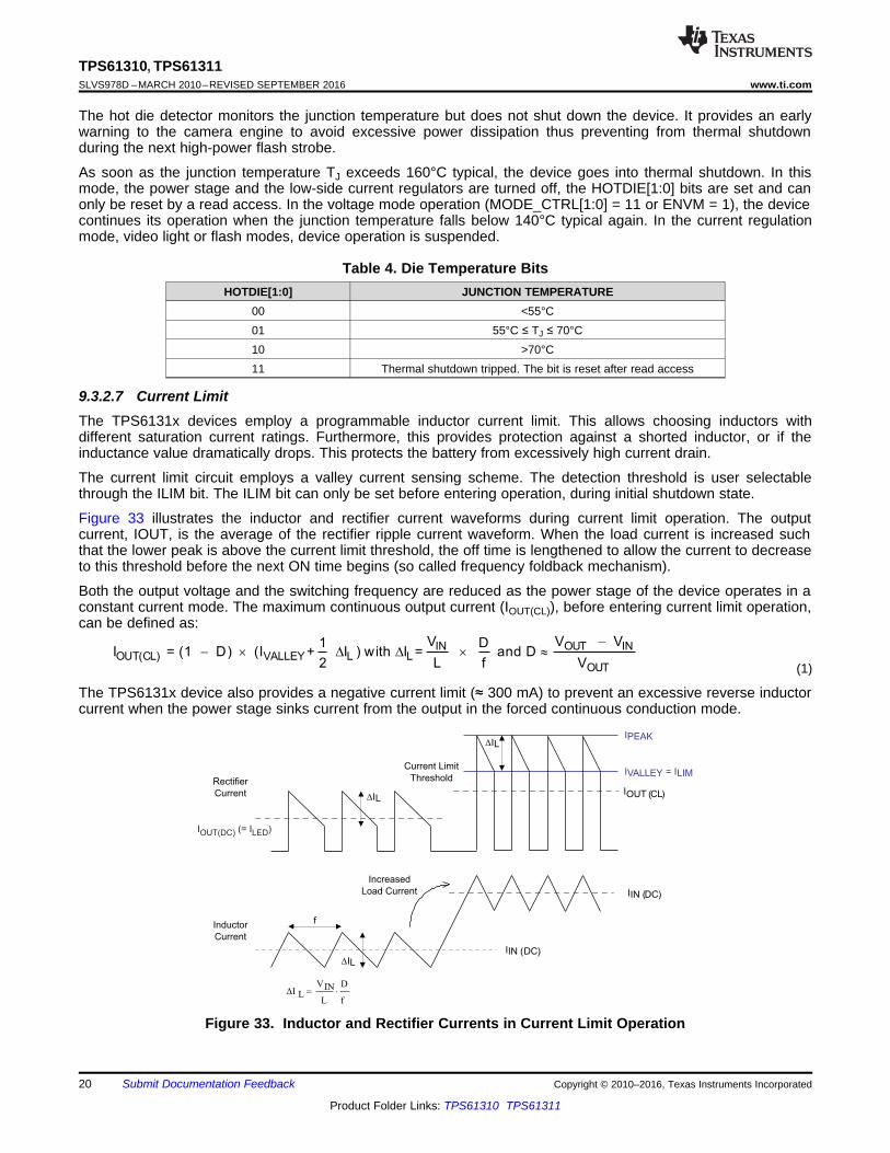
9.3.2.7 Current LimitThe TPS6131x devices employ a programmable inductor current limit. This allows choosing inductors withdifferent saturation current ratings. Furthermore, this provides protection against a shorted inductor, or if theinductance value dramatically drops. This protects the battery from excessively high current drain.
The current limit circuit employs a valley current sensing scheme. The detection threshold is user selectablethrough the ILIM bit. The ILIM bit can only be set before entering operation, during initial shutdown state.
Figure 33 illustrates the inductor and rectifier current waveforms during current limit operation. The outputcurrent, IOUT, is the average of the rectifier ripple current waveform. When the load current is increased suchthat the lower peak is above the current limit threshold, the off time is lengthened to allow the current to decreaseto this threshold before the next ON time begins (so called frequency foldback mechanism).
Both the output voltage and the switching frequency are reduced as the power stage of the device operates in aconstant current mode. The maximum continuous output current (IOUT(CL)), before entering current limit operation,can be defined as:
(1)
The TPS6131x device also provides a negative current limit (≈ 300 mA) to prevent an excessive reverse inductorcurrent when the power stage sinks current from the output in the forced continuous conduction mode.
Figure 33. Inductor and Rectifier Currents in Current Limit Operation

FLASH
DC LIGHT
LED CURRENT
STRB0
Tx- MASK
21
TPS61310, TPS61311www.ti.com SLVS978D –MARCH 2010–REVISED SEPTEMBER 2016
Product Folder Links: TPS61310 TPS61311
Submit Documentation FeedbackCopyright © 2010–2016, Texas Instruments Incorporated
Table 5. Inductor Current Limit OperationCURRENT LIMIT SETTING
ILIM BITTPS61310 TPS613111250 mA 1800 mA Low1750 mA 2480 mA High
9.3.2.8 Flash Blanking (Tx-Mask) for Instantaneous Flash Current ReductionThe TPS6131x devices offer a dedicated hardware signal input (Tx-Mask) that can be used to reduce the flashcurrent to the programmed video light level instantaneously.
This feature can be used to reduce the overall current drawn from the battery if other system components requirehigh energy simultaneously, such as during a RF PA transmission pulse.
The Tx-MASK function has no influence on the safety timer duration.
Figure 34. Synchronized Flash With Blanking Periods (STRB1 = 0)
9.3.3 Start-Up SequenceTo avoid high inrush current during start-up, control the inrush current. When the device enables, the internalstart-up cycle starts with the first step, the precharge phase.
During precharge, the rectifying switch is turned on until the output capacitor is either charged to a value close tothe input voltage or ≈ 3.3 V, whichever occurs first. The rectifying switch is current limited during that phase. Thecurrent limit increases with decreasing input-to-output voltage difference. This circuit also limits the output currentunder output short-circuit conditions.
After precharging the output capacitor, the device starts switching, and increases its current limit in three steps oftypically 25 mA, 250 mA and full current limit (ILIM setting). The current limit transition from the first to thesecond step occurs after 1 ms of operation. Full current limit operation is set once the output voltage reaches itsregulation limits. In this mode, the active balancing circuit is disabled.
9.3.4 NRESET Input: Hardware Enable or DisableThe TPS6131x family features a hardware reset pin (NRESET). This reset pin allows the device to be disabledby an external controller without requiring an I2C write command. Under normal operation, the NRESET pin mustbe held high to prevent an unwanted reset. When the NRESET is driven low, the I2C control interface and allinternal control registers are reset to the default states and the part enters shutdown mode.
Data linestable;
data valid
DATA
CLK
Changeof dataallowed
START Condition
DATA
CLK
STOP Condition
S P
22
TPS61310, TPS61311SLVS978D –MARCH 2010–REVISED SEPTEMBER 2016 www.ti.com
Product Folder Links: TPS61310 TPS61311
Submit Documentation Feedback Copyright © 2010–2016, Texas Instruments Incorporated
9.3.5 Serial Interface DescriptionI2C™ is a 2-wire serial interface developed by Philips Semiconductor, now NXP Semiconductors [1]. The busconsists of a data line (SDA) and a clock line (SCL) with pullup structures. When the bus is idle, both SDA andSCL lines are pulled high. All the I2C compatible devices connect to the I2C bus through open drain I/O pins,SDA and SCL. A master device, usually a microcontroller or a digital signal processor, controls the bus. Themaster is responsible for generating the SCL signal and device addresses. The master also generates specificconditions that indicate the START and STOP of data transfer. A slave device receives or transmits data on thebus under control of the master device.
The TPS6131x device works as a slave and supports these data transfer modes, as defined in the I2C BusSpecification: standard mode (100 kbps) and fast mode (400 kbps), and high-speed mode (3.4 Mbps). Theinterface adds flexibility to the power supply solution, enabling most functions to be programmed to new valuesdepending on the instantaneous application requirements. Register contents remain intact as long as supplyvoltage remains above 2.1 V.
The data transfer protocol for standard and fast modes is exactly the same, therefore they are referred to as F/S-mode in this document. The protocol for high-speed mode is different from F/S-mode, and it is referred to as H/S-mode. The TPS6131x device supports 7-bit addressing; 10-bit addressing and general call address are notsupported. The device 7-bit address is defined as 011 0011.
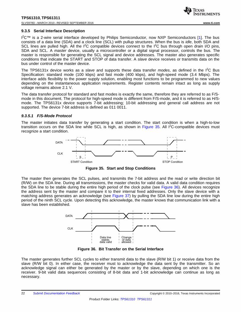
9.3.5.1 F/S-Mode ProtocolThe master initiates data transfer by generating a start condition. The start condition is when a high-to-lowtransition occurs on the SDA line while SCL is high, as shown in Figure 35. All I2C-compatible devices mustrecognize a start condition.
Figure 35. Start and Stop Conditions
The master then generates the SCL pulses, and transmits the 7-bit address and the read or write direction bit(R/W) on the SDA line. During all transmissions, the master checks for valid data. A valid data condition requiresthe SDA line to be stable during the entire high period of the clock pulse (see Figure 36). All devices recognizethe address sent by the master and compare it to their internal fixed addresses. Only the slave device with amatching address generates an acknowledge (see Figure 37) by pulling the SDA line low during the entire highperiod of the ninth SCL cycle. Upon detecting this acknowledge, the master knows that communication link with aslave has been established.
Figure 36. Bit Transfer on the Serial Interface
The master generates further SCL cycles to either transmit data to the slave (R/W bit 1) or receive data from theslave (R/W bit 0). In either case, the receiver must to acknowledge the data sent by the transmitter. So anacknowledge signal can either be generated by the master or by the slave, depending on which one is thereceiver. 9-bit valid data sequences consisting of 8-bit data and 1-bit acknowledge can continue as long asnecessary.
23
TPS61310, TPS61311www.ti.com SLVS978D –MARCH 2010–REVISED SEPTEMBER 2016
Product Folder Links: TPS61310 TPS61311
Submit Documentation FeedbackCopyright © 2010–2016, Texas Instruments Incorporated
To signal the end of the data transfer, the master generates a stop condition by pulling the SDA line from low tohigh while the SCL line is high (see Figure 35). This releases the bus and stops the communication link with theaddressed slave. All I2C compatible devices must recognize the stop condition. Upon the receipt of a stopcondition, all devices know that the bus is released, and they wait for a start condition followed by a matchingaddress.
Attempting to read data from register addresses not listed in this section results in 00h being read out.
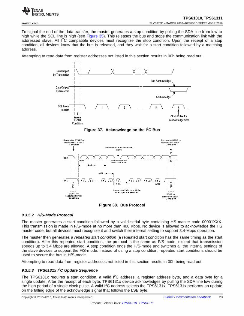
Figure 37. Acknowledge on the I2C Bus
Figure 38. Bus Protocol
9.3.5.2 H/S-Mode ProtocolThe master generates a start condition followed by a valid serial byte containing HS master code 00001XXX.This transmission is made in F/S-mode at no more than 400 Kbps. No device is allowed to acknowledge the HSmaster code, but all devices must recognize it and switch their internal setting to support 3.4-Mbps operation.
The master then generates a repeated start condition (a repeated start condition has the same timing as the startcondition). After this repeated start condition, the protocol is the same as F/S-mode, except that transmissionspeeds up to 3.4 Mbps are allowed. A stop condition ends the H/S-mode and switches all the internal settings ofthe slave devices to support the F/S-mode. Instead of using a stop condition, repeated start conditions should beused to secure the bus in H/S-mode.
Attempting to read data from register addresses not listed in this section results in 00h being read out.
9.3.5.3 TPS6131x I2C Update SequenceThe TPS6131x requires a start condition, a valid I2C address, a register address byte, and a data byte for asingle update. After the receipt of each byte, TPS6131x device acknowledges by pulling the SDA line low duringthe high period of a single clock pulse. A valid I2C address selects the TPS6131x. TPS6131x performs an updateon the falling edge of the acknowledge signal that follows the LSB byte.
Slave Address R/W A Register Address A PSr
1 7 1 1 1 18
Data
8
A/A
1
S HS-Master Code A
1 18
F/S Mode HS Mode F/S Mode
Data Transferred
(n x Bytes + Acknowledge)HS Mode Continues
Slave AddressSr
From Master to TPS6131x
From TPS6131x to Master
A = Acknowledge
A = Acknowledge
S = START condition
Sr = REPEATED START condition
P = STOP condition
Slave Address R/W A Register Address A Data A PS
1 7 1 1 1 1 18 8
“0” Write
Sr
1
Slave Address R/W
7 1
“1” Read
A
1
From Master to TPS6131x
From TPS6131x to Master
A = Acknowledge
S = START condition
Sr = REPEATED START condition
P = STOP condition
Slave Address R/W A Register Address A Data A PS
1 7 1 1 1 1 18 8
“0” Write
From Master to TPS6131x
From TPS6131x to Master
A = Acknowledge
S = START condition
Sr = REPEATED START condition
P = STOP condition
24
TPS61310, TPS61311SLVS978D –MARCH 2010–REVISED SEPTEMBER 2016 www.ti.com
Product Folder Links: TPS61310 TPS61311
Submit Documentation Feedback Copyright © 2010–2016, Texas Instruments Incorporated
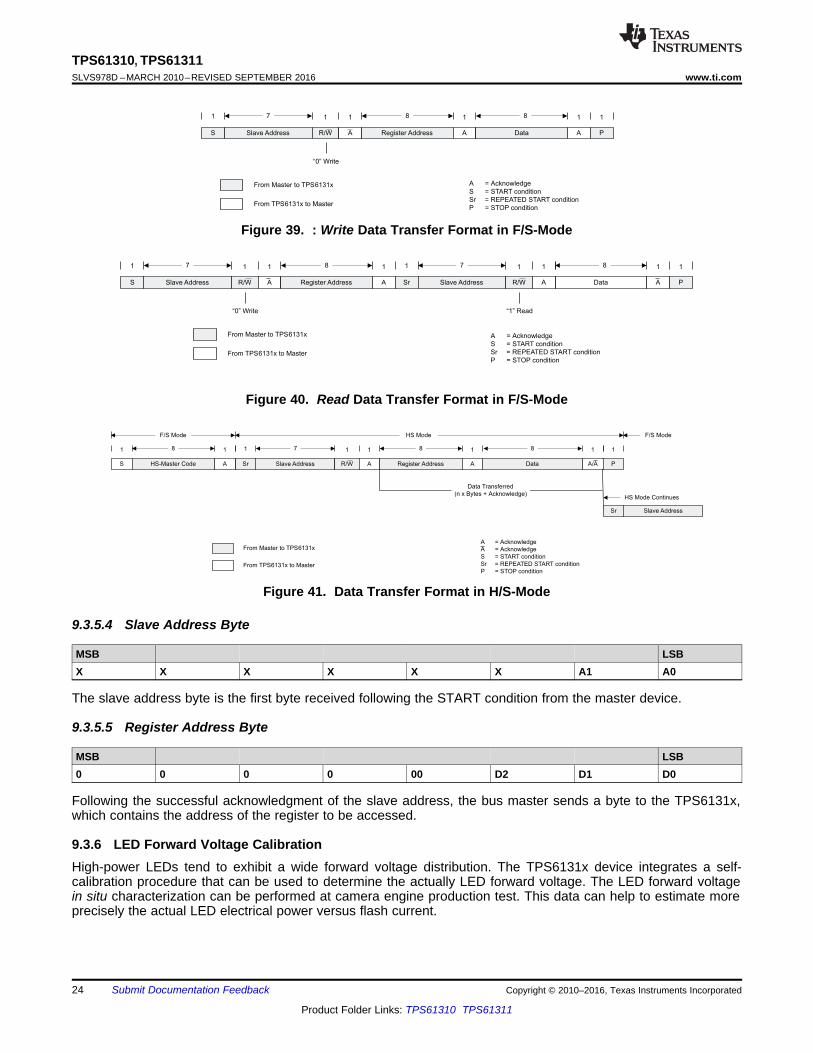
Figure 39. : Write Data Transfer Format in F/S-Mode
Figure 40. Read Data Transfer Format in F/S-Mode
Figure 41. Data Transfer Format in H/S-Mode
9.3.5.4 Slave Address Byte
MSB LSBX X X X X X A1 A0
The slave address byte is the first byte received following the START condition from the master device.
9.3.5.5 Register Address Byte
MSB LSB0 0 0 0 00 D2 D1 D0
Following the successful acknowledgment of the slave address, the bus master sends a byte to the TPS6131x,which contains the address of the register to be accessed.
9.3.6 LED Forward Voltage CalibrationHigh-power LEDs tend to exhibit a wide forward voltage distribution. The TPS6131x device integrates a self-calibration procedure that can be used to determine the actually LED forward voltage. The LED forward voltagein situ characterization can be performed at camera engine production test. This data can help to estimate moreprecisely the actual LED electrical power versus flash current.
Output Voltage, VOUT
Power Good, PG
VBAT
LED Flash Current, IFLASH
OV[3:0] 0000 0001 0010 0011 0100 0101
~200 ms
Feedback Sense Comparator Output
VLED > 400 mV
Self-Calibration,
SELFCAL bit (write)
Self-Calibration,
SELFCAL bit (read)
ESR x ILED~200 ms
Feedback Sense
Comparator Information
X
25
TPS61310, TPS61311www.ti.com SLVS978D –MARCH 2010–REVISED SEPTEMBER 2016
Product Folder Links: TPS61310 TPS61311
Submit Documentation FeedbackCopyright © 2010–2016, Texas Instruments Incorporated
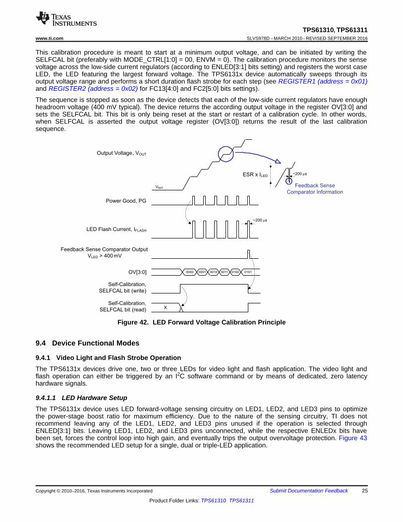
This calibration procedure is meant to start at a minimum output voltage, and can be initiated by writing theSELFCAL bit (preferably with MODE_CTRL[1:0] = 00, ENVM = 0). The calibration procedure monitors the sensevoltage across the low-side current regulators (according to ENLED[3:1] bits setting) and registers the worst caseLED, the LED featuring the largest forward voltage. The TPS6131x device automatically sweeps through itsoutput voltage range and performs a short duration flash strobe for each step (see REGISTER1 (address = 0x01)and REGISTER2 (address = 0x02) for FC13[4:0] and FC2[5:0] bits settings).
The sequence is stopped as soon as the device detects that each of the low-side current regulators have enoughheadroom voltage (400 mV typical). The device returns the according output voltage in the register OV[3:0] andsets the SELFCAL bit. This bit is only being reset at the start or restart of a calibration cycle. In other words,when SELFCAL is asserted the output voltage register (OV[3:0]) returns the result of the last calibrationsequence.
Figure 42. LED Forward Voltage Calibration Principle
9.4 Device Functional Modes
9.4.1 Video Light and Flash Strobe OperationThe TPS6131x devices drive one, two or three LEDs for video light and flash application. The video light andflash operation can either be triggered by an I2C software command or by means of dedicated, zero latencyhardware signals.
9.4.1.1 LED Hardware SetupThe TPS6131x device uses LED forward-voltage sensing circuitry on LED1, LED2, and LED3 pins to optimizethe power-stage boost ratio for maximum efficiency. Due to the nature of the sensing circuitry, TI does notrecommend leaving any of the LED1, LED2, and LED3 pins unused if the operation is selected throughENLED[3:1] bits. Leaving LED1, LED2, and LED3 pins unconnected, while the respective ENLEDx bits havebeen set, forces the control loop into high gain, and eventually trips the output overvoltage protection. Figure 43shows the recommended LED setup for a single, dual or triple-LED application.

TPS6131x
VOUT
COUT
LED1LED2LED3
TPS6131x
VOUT
COUT
LED1LED2LED3
TPS6131x
VOUT
COUT
LED1LED2LED3
Single LED Dual LED Tripple LED
26
TPS61310, TPS61311SLVS978D –MARCH 2010–REVISED SEPTEMBER 2016 www.ti.com
Product Folder Links: TPS61310 TPS61311
Submit Documentation Feedback Copyright © 2010–2016, Texas Instruments Incorporated
Device Functional Modes (continued)
Figure 43. White LED Hardware Setup Options
The LED1, LED2, and LED3 inputs may be connected together to drive one or two LEDs at higher currents.Connecting the current sink inputs in parallel does not affect the internal operation of the TPS6131x. For bestoperation, TI recommends disabling the LED inputs that are not connected. (see the ENLED[3:1] bits descriptionin REGISTER5 (address = 0x05)).
The video light currents are individually programmed through the video light control bits DCL13[2:0] andDCL2[2:0] , the flash currents through FC2[5:0] and FC13[4:0] bits accordingly. If, for single or dual LEDapplication as shown in Figure 43, current sinks are connected to each other and enabled, the resulting video orflash current is the sum of the programmed currents.
9.4.1.2 Triggering Video Light and FlashFor most flexible system integration, the TPS6131x offers several options for activating the video light and flash.Depending on the settings of the MODE_CTRL[1:0] bits, the device can enter different modes of operation. Itoffers the option of triggering the video light and flash through hardware signals (STRB0, STRB1) or software I2Ccommand. The flash-signal hardware trigger can be on the leading-edge, turning on for the programmed flash ontime, or level sensitive, turning on for as long as the signal is logic high.
The TPS6131x flash timer is programmed through the STIM[2:0] and SELSTIM bits. If the flash is fired by arising-edge trigger or by an I2C command, the timer defines the flash duration. If the flash is fired by a level-sensitive trigger, the timer defines the maximum flash ON duration, and overrides the hardware signal if theprogrammed on-time is exceeded.
For video lighting, a watchdog timer is implemented; this must be refreshed within 13 seconds. This function canbe disabled, as described in Table 6.
Table 6. Mode Operations for Video Light and FlashMODE_CTRL SETTING DESCRIPTION
MODE_CTRL[1:0] = 01
The STRB0, STRB1 inputs are disabled. The device regulates the LED current in video light mode(DCLC bits) regardless of the STRB0, STRB1 inputs and the START_FLASH/TIMER (SFT) bit. To avoiddevice shutdown because of the video light safety timeout, MODE_CTRL[1:0] must be refreshed withinless than 13 seconds (STRB1 = 0). The video light watchdog timer can be disabled by pulling theSTRB1 signal high.
MODE_CTRL[1:0] = 10
The STRB0, STRB1 inputs are enabled. The flash pulse can be triggered by these synchronizationsignals, or by a software command (START_FLASH/TIMER (SFT) bit). The LEDs are enabled ordisabled according to the STRB0, STRB1 input. The flash safety timer is activated, and the video lightwatchdog timer is disabled.
The dual-wire camera-module interface STRB0 and STRB1 inputs are used for selecting the video light(STRB1 = 1) or flash (STRB1 = 0) mode. The STRB0 signal then triggers the video light or flash, depending onthe state of STRB1. The STT bit defines if the flash trigger is level sensitive (STT = 0), or fired on the rising edge(STT = 1).

STRB0
AF ASSIST LIGHT STROBE
STRB1
TIMERDURATION = STIM
LED CONTROL
DC LIGHT FLASH
LED OFF LED OFF LED OFF
STRB0
AF ASSIST LIGHT STROBE
STRB1
TIMERDURATION < STIM
LED CONTROL
DC LIGHT FLASH
LED OFF LED OFF LED OFF
27
TPS61310, TPS61311www.ti.com SLVS978D –MARCH 2010–REVISED SEPTEMBER 2016
Product Folder Links: TPS61310 TPS61311
Submit Documentation FeedbackCopyright © 2010–2016, Texas Instruments Incorporated
9.4.1.3 Level-Sensitive Flash Trigger (STT = 0)In this mode, the high-power LEDs are driven at the flash current level and the safety timer (STIM) is running.The maximum duration of the flash pulse is defined in the STIM[2:0] register.
The safety timer is triggered on rising edge and stopped by a negative logic on the synchronization source(STRB0, STRB1 = 0) or by a timeout event (TO bit).
Figure 44. Hardware Synchronized Video Light and Flash Strobe
9.4.1.4 Rising-Edge Flash Trigger (STT = 1)In this mode, the high-power LEDs are driven at the flash current level and the safety timer (STIM) is running.The duration of the flash pulse is defined in the STIM[2:0] register.
The flash strobe is started either by a rising edge on the synchronization source (STRB0 = 1, STRB1 = 0) or by apositive transition on the START-FLASH/TIMER (SFT) bit (STRB0 = 1, STRB1 = 0). Once running, the timerignores all kind of triggering signals and only stops after a timeout (TO). START-FLASH/TIMER (SFT) bit is beingreset by the timeout (TO) signal.
Figure 45. Edge Sensitive Timer (Single Trigger Event)
9.4.2 Voltage ModeIn this mode, the TPS6131x operates as a standard voltage-boost regulator, featuring power-save mode forimproved efficiency under light loads. The voltage-mode operation is enabled by software control by setting themode-control bit MODE_CTRL[1:0] = 11. The device regulates a constant output voltage according to theOV[3:0] bit settings (from 3.825 V to 5.7 V in 125-mV steps). In voltage mode, the LED current sinks LED1,LED2, and LED3 are turned off.
The TPS6131x integrates a software control bit (ENVM bit) that can be used to force the converter to run involtage mode. This enables the converter to operate at a fixed programmed output voltage (according to theOV[3:0] settings) while operating the LEDs.
Table 7 provides an overview of the different voltage mode variations.

28
TPS61310, TPS61311SLVS978D –MARCH 2010–REVISED SEPTEMBER 2016 www.ti.com
Product Folder Links: TPS61310 TPS61311
Submit Documentation Feedback Copyright © 2010–2016, Texas Instruments Incorporated
Table 7. Voltage Mode DescriptionINTERNAL REGISTER
SETTINGS MODE_CTRL[1:0]ENVM
BIT OPERATING MODES
11 0 LEDs are turned off and the converter operate in voltage-regulation mode (VM); the outputvoltage is set through register OV[3:0].00 1
01 1
The converter operates in voltage-regulation mode (VM); the output voltage is set through theregister OV[3:0]. The LEDs are turned on for video light operation and the energy is beingdirectly transferred from the battery to the output. The LED currents are regulated by the meansof the low-side current sinks.
10 1The converter operates in the voltage-regulation mode (VM); the output voltage is set throughthe register OV[3:0]. The LED currents are regulated by the low-side current sinks. The LEDsare ready for flash operation.
11 1 LEDs are turned off and the converter operates in the voltage regulation mode (VM); the outputvoltage is set through the register OV[3:0].
9.4.2.1 Down Mode in Voltage Mode OperationIn general, a boost converter only regulates output voltages which are higher than the input voltage. TheTPS6131x can regulate 4.2 V at the output with an input voltage as high as 5.5 V. To control these applicationsproperly, a down-conversion mode is implemented.
In voltage-regulation mode, if the input voltage reaches or exceeds the output voltage, the converter changes todown-conversion mode. In this mode, the control circuit changes the behavior of the rectifying PMOS. It sets thevoltage drop across the PMOS as high as required to regulate the output voltage. This increases the powerlosses in the converter, and must be considered for thermal design. The down-conversion mode is automaticallyturned off as soon as the input voltage falls to approximately 200 mV below the output voltage.
For proper operation in down-conversion mode the output voltage must not be programmed higher thanapproximately 5.3 V. Take care not to violate the absolute maximum ratings at the SW pins.
9.4.2.2 Power Good IndicationThe TPS6131x integrates a Power Good circuit that is activated when the device operates in voltage-regulationmode (MODE_CTRL[1:0] = 11 or ENVM = 1). In shutdown mode (MODE_CTRL[1:0] = 00, ENVM = 0), theGPIO/PG pin state is defined below, according to the GPIOTYPE bit:
Table 8. GPIO/PG State in ShutdownGPIOTYPE GPIO/PG SHUTDOWN STATE
0 Reset or pulled to ground1 Open-drain
Depending on the GPIO/PG output stage type selection, push-pull or open-drain, the polarity of the Power Goodoutput signal (PG) can be inverted or not. The Power Good software bit and hardware signal polarity is definedbelow:
Table 9. Power Good Signal PolarityGPIOTYPE PG BIT GPIO/PG OUTPUT PORT COMMENTS
0: push-pull output0 0
Output is active-high1 1
1: open-drain output0 Open-drain
Output is active-low1 Low
VOUT NOM.
PFM mode at light load
PWM mode at heavy load
PFM ripple about 0.015 x VOUT
1.013 x VOUT NOM.
Output
Voltage
Voltage Mode Request
Output Voltage, VOUT
Nom.Voltage
Start-up phase
Power Good Bit, (PG)
Power Good Output,GPIO/PG
Hi-Z Hi-Z
1.025 VOUT (NOM)
0.985 VOUT (NOM)
VOUT (NOM)
Output Voltage
Down Regulation
Output Voltage
Up Regulation
Forced PWM mode operation
Forced PWM mode operation
(PG)Bit
29
TPS61310, TPS61311www.ti.com SLVS978D –MARCH 2010–REVISED SEPTEMBER 2016
Product Folder Links: TPS61310 TPS61311
Submit Documentation FeedbackCopyright © 2010–2016, Texas Instruments Incorporated
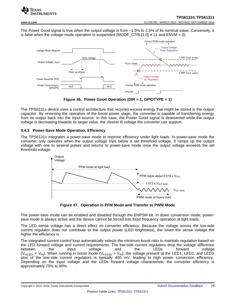
The Power Good signal is true when the output voltage is from –1.5% to 2.5% of its nominal value. Conversely, itis false when the voltage-mode operation is suspended (MODE_CTRL[1:0] ≠ 11 and ENVM = 0).
Figure 46. Power Good Operation (DIR = 1, GPIOTYPE = 1)
The TPS6131x device uses a control architecture that recycles excess energy that might be stored in the outputcapacitor. By reversing the operation of the boost power stage, the converter is capable of transferring energyfrom its output back into the input source. In this case, the Power Good signal is deasserted while the outputvoltage is decreasing towards its target value, the closest fit voltage the converter can support.
9.4.3 Power-Save Mode Operation, EfficiencyThe TPS6131x integrates a power-save mode to improve efficiency under light loads. In power-save mode theconverter only operates when the output voltage trips below a set threshold voltage. It ramps up the outputvoltage with one to several pulses and returns to power-save mode once the output voltage exceeds the setthreshold voltage.
Figure 47. Operation in PFM Mode and Transfer to PWM Mode
The power-save mode can be enabled and disabled through the ENPSM bit. In down conversion mode, power-save mode is always active and the device cannot be forced into fixed frequency operation at light loads.
The LED sense voltage has a direct effect on converter efficiency. Because the voltage across the low-sidecurrent regulator does not contribute to the output power (LED brightness), the lower the sense voltage thehigher the efficiency is.
The integrated current control loop automatically selects the minimum boost ratio to maintain regulation based onthe LED forward voltage and current requirements. The low-side current regulators drop the voltage differencebetween the input voltage and the LEDs forward voltage(VF(LED) < VIN). When running in boost mode (VF(LED) > VIN), the voltage present at the LED1, LED2, and LED3pins of the low-side current regulators is typically 400 mV, leading to high power conversion efficiency.Depending on the input voltage and the LEDs forward voltage characteristic the converter efficiency isapproximately 75% to 90%.
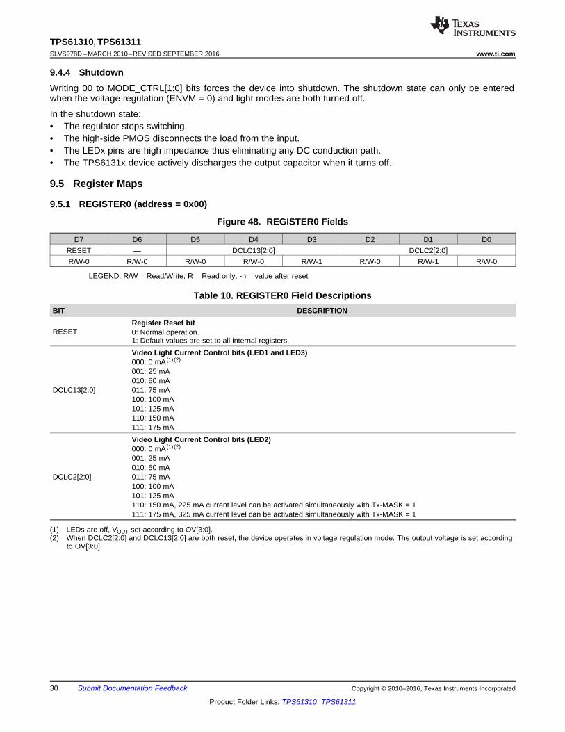
30
TPS61310, TPS61311SLVS978D –MARCH 2010–REVISED SEPTEMBER 2016 www.ti.com
Product Folder Links: TPS61310 TPS61311
Submit Documentation Feedback Copyright © 2010–2016, Texas Instruments Incorporated
9.4.4 ShutdownWriting 00 to MODE_CTRL[1:0] bits forces the device into shutdown. The shutdown state can only be enteredwhen the voltage regulation (ENVM = 0) and light modes are both turned off.
In the shutdown state:• The regulator stops switching.• The high-side PMOS disconnects the load from the input.• The LEDx pins are high impedance thus eliminating any DC conduction path.• The TPS6131x device actively discharges the output capacitor when it turns off.
9.5 Register Maps
9.5.1 REGISTER0 (address = 0x00)
Figure 48. REGISTER0 Fields
D7 D6 D5 D4 D3 D2 D1 D0RESET — DCLC13[2:0] DCLC2[2:0]R/W-0 R/W-0 R/W-0 R/W-0 R/W-1 R/W-0 R/W-1 R/W-0
LEGEND: R/W = Read/Write; R = Read only; -n = value after reset
(1) LEDs are off, VOUT set according to OV[3:0].(2) When DCLC2[2:0] and DCLC13[2:0] are both reset, the device operates in voltage regulation mode. The output voltage is set according
to OV[3:0].
Table 10. REGISTER0 Field DescriptionsBIT DESCRIPTION
RESETRegister Reset bit0: Normal operation.1: Default values are set to all internal registers.
DCLC13[2:0]
Video Light Current Control bits (LED1 and LED3)000: 0 mA (1) (2)
001: 25 mA010: 50 mA011: 75 mA100: 100 mA101: 125 mA110: 150 mA111: 175 mA
DCLC2[2:0]
Video Light Current Control bits (LED2)000: 0 mA (1) (2)
001: 25 mA010: 50 mA011: 75 mA100: 100 mA101: 125 mA110: 150 mA, 225 mA current level can be activated simultaneously with Tx-MASK = 1111: 175 mA, 325 mA current level can be activated simultaneously with Tx-MASK = 1

31
TPS61310, TPS61311www.ti.com SLVS978D –MARCH 2010–REVISED SEPTEMBER 2016
Product Folder Links: TPS61310 TPS61311
Submit Documentation FeedbackCopyright © 2010–2016, Texas Instruments Incorporated
9.5.2 REGISTER1 (address = 0x01)
Figure 49. REGISTER1 Fields
D7 D6 D5 D4 D3 D2 D1 D0MODE_CTRL[1:0] FC2[5:0]
R/W-0 R/W-0 R/W-0 R/W-1 R/W-0 R/W-0 R/W-0 R/W-0
LEGEND: R/W = Read/Write; R = Read only; -n = value after reset
(1) LEDs are off, VOUT set according to OV[3:0].(2) When FC13[4:0] and FC2[5:0] are both reset, the device operates in voltage regulation mode. The output voltage is set according to
OV[3:0].
Table 11. REGISTER1 Field DescriptionsBIT DESCRIPTION
MODE_CTRL[1:0]
Mode Control bits00: Device in shutdown mode.01: Device operates in video light mode.10: Device operates in flash mode.11: Device operates as constant voltage source.To avoid device shutdown by video light safety timeout, MODE_CTRL[1:0] bits must be refreshed within less than13 s.Writing to REGISTER1[7:6] automatically updates REGISTER2[7:6].
FC2[5:0]
Flash Current Control bits (LED2)000000: 0 mA (1) (2)
000001: 25 mA000010: 50 mA000011: 75 mA000100: 100 mA000101: 125 mA000110: 150 mA000111: 175 mA001000: 200 mA001001: 225 mA001010: 250 mA001011: 275 mA001100: 300 mA001101: 325 mA001110: 350 mA001111: 375 mA010000: 400 mA010001: 425 mA010010: 450 mA010011: 475 mA010100: 500 mA010101: 525 mA010110: 550 mA010111: 575 mA011000: 600 mA011001: 625 mA011010: 650 mA011011: 675 mA011100: 700 mA011101: 725 mA011110: 750 mA011111: 775 mA100000 to 111111: 800 mA

32
TPS61310, TPS61311SLVS978D –MARCH 2010–REVISED SEPTEMBER 2016 www.ti.com
Product Folder Links: TPS61310 TPS61311
Submit Documentation Feedback Copyright © 2010–2016, Texas Instruments Incorporated
9.5.3 REGISTER2 (address = 0x02)
Figure 50. REGISTER2 Fields
D7 D6 D5 D4 D3 D2 D1 D0MODE_CTRL[1:0] ENVM FC13[4:0]
R/W-0 R/W-0 R/W-0 R/W-0 R/W-1 R/W-0 R/W-0 R/W-0
LEGEND: R/W = Read/Write; R = Read only; -n = value after reset
(1) LEDs are off, VOUT set according to OV[3:0].(2) When FC13[4:0] and FC2[5:0] are both reset, the device operates in voltage regulation mode. The output voltage is set according to
OV[3:0].
Table 12. REGISTER2 Field DescriptionsBIT DESCRIPTION
MODE_CTRL[1:0]
Mode Control bits00: Device in shutdown mode.01: Device operates in video light mode.10: Device operates in flash mode.11: Device operates as constant voltage source.To avoid device shutdown by video light safety timeout, MODE_CTRL[1:0] bits must be refreshed within less than13 s.Writing to REGISTER2[6:5] automatically updates REGISTER1[6:5].
ENVM
Enable Voltage Mode bit.0: Normal operation.1: Forces the device into a constant voltage source.In read mode, the ENVM bit is automatically updated to reflect the logic state of the ENVM input pin.
FC13[4:0]
Flash Current Control bits (LED1 and LED3)00000: 0 mA (1) (2)
00001: 25 mA00010: 50 mA00011: 75 mA00100: 100 mA00101: 125 mA00110: 150 mA00111: 175 mA01000: 200 mA01001: 225 mA01010: 250 mA01011: 275 mA01100: 300 mA01101: 325 mA01110: 350 mA01111: 375 mA10000 to 11111: 400 mA

33
TPS61310, TPS61311www.ti.com SLVS978D –MARCH 2010–REVISED SEPTEMBER 2016
Product Folder Links: TPS61310 TPS61311
Submit Documentation FeedbackCopyright © 2010–2016, Texas Instruments Incorporated
9.5.4 REGISTER3 (address = 0x03)
Figure 51. REGISTER3 Fields
D7 D6 D5 D4 D3 D2 D1 D0
STIM[2:0] HPFL SELSTIM (W)TO (R) STT SFT Tx-MASK
R/W-1 R/W-1 R/W-0 R-0 R-0 R/W-0 R/W-0 R/W-1
LEGEND: R/W = Read/Write; R = Read only; -n = value after resetTable 13. REGISTER3 Field Descriptions
BIT DESCRIPTION
STIM[2:0]
Safety Timer bitsSTIM[2:0]000001010011100101110111
RANGE 068.2 ms102.2 ms136.3 ms170.4 ms204.5 ms340.8 ms579.3 ms852 ms
RANGE 15.3 ms10.7 ms16 ms21.3 ms26.6 ms32 ms37.3 ms71.5 ms
HPFL
High-Power LED Failure flag0: Proper LED operation.1: LED failed (open or shorted).High-power LED failure flag is reset after readout
SELSTIMSafety Timer Selection Range (Write Only)0: Safety timer range 0.1: Safety timer range 1.
TOTime-Out Flag (Read Only)0: No time-out event occurred.1: Time-out event occurred. Time-out flag is reset at restart of the safety timer.
STT
Safety Timer Trigger bit0: LED safety timer is level sensitive.1: LED safety timer is rising edge sensitive.This bit is only valid for MODE_CTRL[1:0] = 10.
SFT
Start/Flash Timer bitIn write mode, this bit initiates a flash strobe sequence. Notice that this bit is only active when STRB0 input is high.0: No change in the high-power LED current.1: High-power LED current ramps to the flash current level.In read mode, this bit indicates the high-power LED status.0: High-power LEDs are idle.1: Ongoing high-power LED flash strobe.
Tx-MASK
Flash Blanking Control bitIn write mode, this bit enables and disables the flash blanking and LED current reduction function.0: Flash blanking disabled.1: LED current is reduced to video light level when Tx-MASK input is high.In read mode, this flag indicates whether or not the flash masking input is activated. Tx-MASK flag is reset afterreadout of the flag.0: No flash blanking event occurred.1: Tx-MASK input triggered.
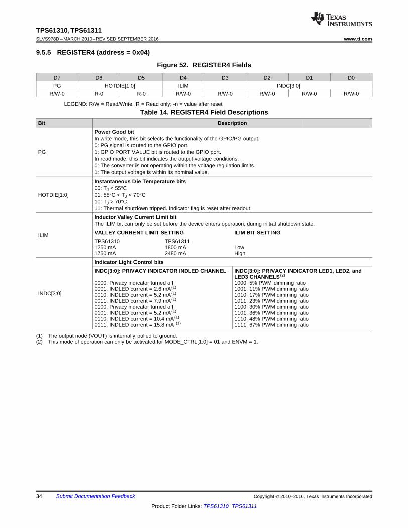
34
TPS61310, TPS61311SLVS978D –MARCH 2010–REVISED SEPTEMBER 2016 www.ti.com
Product Folder Links: TPS61310 TPS61311
Submit Documentation Feedback Copyright © 2010–2016, Texas Instruments Incorporated
9.5.5 REGISTER4 (address = 0x04)
Figure 52. REGISTER4 Fields
D7 D6 D5 D4 D3 D2 D1 D0PG HOTDIE[1:0] ILIM INDC[3:0]
R/W-0 R-0 R-0 R/W-0 R/W-0 R/W-0 R/W-0 R/W-0
LEGEND: R/W = Read/Write; R = Read only; -n = value after reset
(1) The output node (VOUT) is internally pulled to ground.(2) This mode of operation can only be activated for MODE_CTRL[1:0] = 01 and ENVM = 1.
Table 14. REGISTER4 Field DescriptionsBit Description
PG
Power Good bitIn write mode, this bit selects the functionality of the GPIO/PG output.0: PG signal is routed to the GPIO port.1: GPIO PORT VALUE bit is routed to the GPIO port.In read mode, this bit indicates the output voltage conditions.0: The converter is not operating within the voltage regulation limits.1: The output voltage is within its nominal value.
HOTDIE[1:0]
Instantaneous Die Temperature bits00: TJ < 55°C01: 55°C < TJ < 70°C10: TJ > 70°C11: Thermal shutdown tripped. Indicator flag is reset after readout.
ILIM
Inductor Valley Current Limit bitThe ILIM bit can only be set before the device enters operation, during initial shutdown state.VALLEY CURRENT LIMIT SETTING ILIM BIT SETTINGTPS613101250 mA1750 mA
TPS613111800 mA2480 mA
LowHigh
INDC[3:0]
Indicator Light Control bitsINDC[3:0]: PRIVACY INDICATOR INDLED CHANNEL_0000: Privacy indicator turned off0001: INDLED current = 2.6 mA (1)
0010: INDLED current = 5.2 mA (1)
0011: INDLED current = 7.9 mA (1)
0100: Privacy indicator turned off0101: INDLED current = 5.2 mA (1)
0110: INDLED current = 10.4 mA (1)
0111: INDLED current = 15.8 mA (1)
INDC[3:0]: PRIVACY INDICATOR LED1, LED2, andLED3 CHANNELS (2)
1000: 5% PWM dimming ratio1001: 11% PWM dimming ratio1010: 17% PWM dimming ratio1011: 23% PWM dimming ratio1100: 30% PWM dimming ratio1101: 36% PWM dimming ratio1110: 48% PWM dimming ratio1111: 67% PWM dimming ratio

35
TPS61310, TPS61311www.ti.com SLVS978D –MARCH 2010–REVISED SEPTEMBER 2016
Product Folder Links: TPS61310 TPS61311
Submit Documentation FeedbackCopyright © 2010–2016, Texas Instruments Incorporated
9.5.6 REGISTER5 (address = 0x05)
Figure 53. REGISTER5 Fields
D7 D6 D5 D4 D3 D2 D1 D0
SELFCAL ENPSM DIR (W)STSTRB1 (R) GPIO GPIOTYPE ENLED3 ENLED2 ENLED1
R/W-0 R/W-1 R/W-1 R/W-0 R/W-1 R/W-0 R/W-1 R/W-0
LEGEND: R/W = Read/Write; R = Read only; -n = value after resetTable 15. REGISTER5 Field Descriptions
Bit Description
SELFCAL
High-Current LED Forward Voltage Self-Calibration Start bitIn write mode, this bit enables and disables the output voltage versus LED forward voltage and current self-calibration procedure.0: Self-calibration disabled.1: Self-calibration enabled.In read mode, this bit returns the status of the self-calibration procedure.0: Self-calibration ongoing1: Self-calibration done. This bit is only reset at the start or restart of a calibration cycle.
ENPSMEnable and Disable Power-Save Mode bit0: Power-save mode disabled.1: Power-save mode enabled.
STSTRB1 STRB1 Input Status bit (Read Only)This bit indicates the logic state on the STRB1 state.
DIRGPIO Direction bit0: GPIO configured as input.1: GPIO configured as output.
GPIO GPIO Port ValueThis bit contains the GPIO port value.
GPIOTYPEGPIO Port Type0: GPIO is configured as push-pull output.1: GPIO is configured as open-drain output.
ENLED3Enable and Disable High-Current LED3 bit0: LED3 input is disabled.1: LED3 input is enabled.
ENLED2Enable and Disable High-Current LED2 bit0: LED2 input is disabled.1: LED2 input is enabled.
ENLED1Enable and Disable High-Current LED1 bit0: LED1 input is disabled.1: LED1 input is enabled.

36
TPS61310, TPS61311SLVS978D –MARCH 2010–REVISED SEPTEMBER 2016 www.ti.com
Product Folder Links: TPS61310 TPS61311
Submit Documentation Feedback Copyright © 2010–2016, Texas Instruments Incorporated
9.5.7 REGISTER6 (address = 0x06)
Figure 54. REGISTER6 Fields
D7 D6 D5 D4 D3 D2 D1 D0ENTS LEDHOT LEDWARN LEDHDR 0V[3:0]R/W-0 R/W-0 R-0 R-0 R/W-1 R/W-0 R/W-0 R/W-1
LEGEND: R/W = Read/Write; R = Read only; -n = value after resetTable 16. REGISTER6 Field Descriptions
Bit Description
ENTSEnable and Disable LED Temperature Monitoring0: LED temperature monitoring disabled.1: LED temperature monitoring enabled.
LEDHOT
LED Excessive Temperature FlagThis bit can be reset by writing a logic level zero.0: TS input voltage > 0.345 V.1: TS input voltage < 0.345 V.
LEDWARN
LED Temperature Warning Flag (Read Only)This flag is reset after readout.0: TS input voltage > 1.05 V.1: TS input voltage < 1.05 V.
LEDHDR
LED High-Current Regulator Headroom Voltage Monitoring bitThis bit returns the headroom voltage status of the LED high-current regulators. This value is being updated at theend of a flash strobe, before the LED current ramp-down phase.0: Low headroom voltage.1: Sufficient headroom voltage.
0V[3:0]
Output Voltage Selection bitsIn read mode, these bits return the result of the high-current LED forward voltage self-calibration procedure.In write mode, these bits are used to set the target output voltage (see Down Mode in Voltage Mode Operationvoltage regulation mode). In applications requiring dynamic voltage control, take care to set the new target codeafter voltage mode operation is enabled (MODE_CTRL[1:0] = 11 or ENVM bit = 1).OV[3:0]: Target Output Voltage0000: 3.825 V0001: 3.95 V0010: 4.075 V0011: 4.2 V0100: 4.325 V0101: 4.45 V0110: 4.575 V0111: 4.7 V1000: 4.825 V1001: 4.95 V1010: 5.075 V1011: 5.2 V1100: 5.325 V1101: 5.45 V1110: 5.575 V1111: 5.7 V
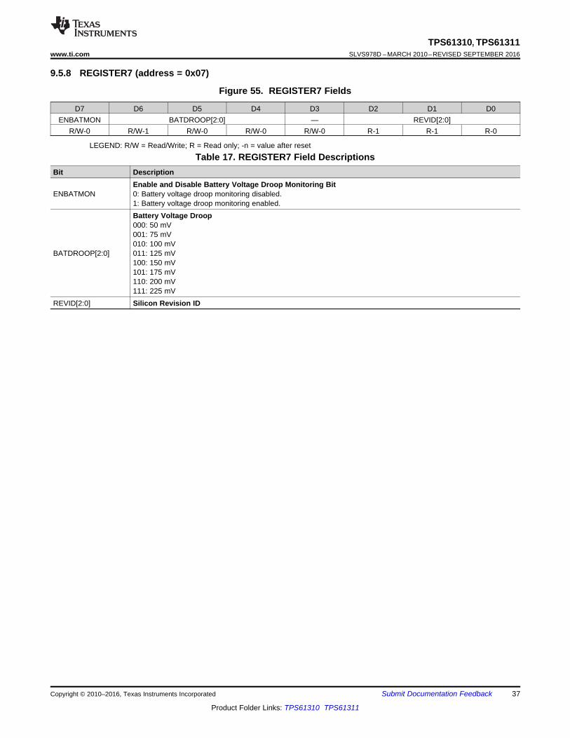
37
TPS61310, TPS61311www.ti.com SLVS978D –MARCH 2010–REVISED SEPTEMBER 2016
Product Folder Links: TPS61310 TPS61311
Submit Documentation FeedbackCopyright © 2010–2016, Texas Instruments Incorporated
9.5.8 REGISTER7 (address = 0x07)
Figure 55. REGISTER7 Fields
D7 D6 D5 D4 D3 D2 D1 D0ENBATMON BATDROOP[2:0] — REVID[2:0]
R/W-0 R/W-1 R/W-0 R/W-0 R/W-0 R-1 R-1 R-0
LEGEND: R/W = Read/Write; R = Read only; -n = value after resetTable 17. REGISTER7 Field Descriptions
Bit Description
ENBATMONEnable and Disable Battery Voltage Droop Monitoring Bit0: Battery voltage droop monitoring disabled.1: Battery voltage droop monitoring enabled.
BATDROOP[2:0]
Battery Voltage Droop000: 50 mV001: 75 mV010: 100 mV011: 125 mV100: 150 mV101: 175 mV110: 200 mV111: 225 mV
REVID[2:0] Silicon Revision ID

CAMERA ENGINEFLASH SYNCHRONIZATION
RF PA TX ACTIVE
VOUT
AVIN
SW
CI
SW
LED 1
CO
10 mF
PGND
PGND
AGND
L
2.2 mH
SDA
SCL
TPS 61310
LED 2
LED 3
D1 D 22 .5 V .. 5 .5 V
STRB0
STRB1
TS GPIO /PG
INDLED
Privacy
IndicatorI2
C I /F
NRESET
220 k
NTC
Tx -MASK
HARDWARE RESET
Copyright © 2016, Texas Instruments Incorporated
38
TPS61310, TPS61311SLVS978D –MARCH 2010–REVISED SEPTEMBER 2016 www.ti.com
Product Folder Links: TPS61310 TPS61311
Submit Documentation Feedback Copyright © 2010–2016, Texas Instruments Incorporated
10 Application and Implementation
NOTEInformation in the following applications sections is not part of the TI componentspecification, and TI does not warrant its accuracy or completeness. TI’s customers areresponsible for determining suitability of components for their purposes. Customers shouldvalidate and test their design implementation to confirm system functionality.
10.1 Application InformationTPS6131x family is based on a high-efficiency synchronous boost topology, which can drive up to three LEDs inparallel. The power stage is capable of supplying a maximum total current up to 1750 mA for TPS61310 and2480 mA for TPS61311. The 2-MHz switching frequency allows the use of small and low passive components.
10.2 Typical Applications
10.2.1 2x 600-mA High Power White LED Solution Featuring Privacy Indicator
Figure 56. 2x 600-mA High Power White LED Solution Featuring Privacy Indicator
10.2.1.1 Design RequirementsIn this design example, different LED current limit is set through I2C interface, the input voltage is 2.5 V to 5.5 V,output voltage is 4.94 V, operating frequency of 2 MHz.

ESROUTERR RIV ´=D
OUT OUT INmin
OUT
I × (V V )C
f V V
-»
´ D ´
OUT OUT ININL(PEAK)
OUT
I V VV DI = + with D =
2 f L (1 D) V
-´
´ ´ - ´ h
OUTL OUT
IN
VI I
η V» ´
´
39
TPS61310, TPS61311www.ti.com SLVS978D –MARCH 2010–REVISED SEPTEMBER 2016
Product Folder Links: TPS61310 TPS61311
Submit Documentation FeedbackCopyright © 2010–2016, Texas Instruments Incorporated
Typical Applications (continued)10.2.1.2 Detailed Design Procedure
10.2.1.2.1 Inductor Selection
A boost converter requires two main passive components for storing energy during the conversion. A boostinductor and a storage capacitor at the output are required.
The TPS6131x device integrates current-limit protection circuitry. The valley current of the PMOS rectifier issensed to limit the maximum current flowing through the synchronous rectifier and the inductor. The valley peakcurrent limit (1250 mA or 1750 mA) is user selectable through the I2C interface.
To optimize solution size the TPS6131x device is designed to operate with inductance values from a minimum of1.3 µH to a maximum of 2.9 µH. TI recommends a 2.2-µH inductance in typical high-current white LEDapplications.
The highest peak current through the inductor and the power switch depends on the output load, the input andoutput voltages. The maximum average inductor current and the maximum inductor peak current can beestimated using Equation 2 and Equation 3:
(2)
where• f = switching frequency (2 MHz)• L = inductance value (2.2 µH)• η = estimated efficiency (85%) (3)
The losses in the inductor caused by magnetic hysteresis losses and copper losses are a major parameter fortotal circuit efficiency.
10.2.1.2.2 Input Capacitor
For good input-voltage filtering, TI recommends low ESR ceramic capacitors. TI recommends a 10-µF inputcapacitor to improve transient behavior of the regulator and EMI behavior of the total power supply circuit. Theinput capacitor must be placed as close as possible to the input pin of the converter.
10.2.1.2.3 Output Capacitor
The major parameter necessary to define the output capacitor is the maximum allowed output-voltage ripple ofthe converter. This ripple is determined by two parameters of the capacitor, the capacitance and the ESR. It ispossible to calculate the minimum capacitance required for the defined ripple, supposing that the ESR is zero, byusing Equation 4:
where• f is the switching frequency• ΔV is the maximum allowed ripple (4)
With a chosen ripple voltage of 10 mV, a minimum capacitance of 10 µF is required. The total ripple is larger dueto the ESR of the output capacitor. This additional component of the ripple can be calculated using Equation 5:
(5)
The total ripple is the sum of the ripple caused by the capacitance and the ripple caused by the ESR of thecapacitor. Additional ripple is caused by load transients. This means that the output capacitor must completelysupply the load during the charging phase of the inductor. A reasonable value of the output capacitance dependson the speed of the load transients and the load current during the load change.

Temperature (°C)
TS
Inpu
t Res
ista
nce
(k:
)
25 35 45 55 65 75 85 95 105 115 1250
10
20
30
40
50
60
70
80
D001
Minimum NTCMaximum NTCTypical NTC
40
TPS61310, TPS61311SLVS978D –MARCH 2010–REVISED SEPTEMBER 2016 www.ti.com
Product Folder Links: TPS61310 TPS61311
Submit Documentation Feedback Copyright © 2010–2016, Texas Instruments Incorporated
Typical Applications (continued)For the standard current white LED application, a minimum of 3-µF effective output capacitance is usuallyrequired when operating with 2.2-µH (typical) inductors. For solution size reasons, this is usually one or moreX5R or X7R ceramic capacitors.
Depending on the material, size and therefore margin to the rated voltage of the used output capacitor,degradation on the effective capacitance can be observed. This loss of capacitance is related to the DC biasvoltage applied. Therefore, TI recommends checking that the selected capacitors show enough effectivecapacitance under real operating conditions.
10.2.1.2.4 NTC Selection
The TPS6131x requires a negative thermistor (NTC) for sensing the LED temperature. Once the temperaturemonitoring feature is activated, a regulated bias current (approximately 24 µA) is driven out of the TS port toproduce a voltage across the thermistor.
If the temperature of the NTC-thermistor rises due to the heat dissipated by the LED, the voltage on the TS inputpin decreases. When this voltage goes below the warning threshold, the LEDWARN bit in REGISTER6 is set.This flag is cleared by reading the register.
If the voltage on the TS input decreases further and falls below hot threshold, the LEDHOT bit in REGISTER6 isset and the device goes automatically in shutdown mode to avoid damaging the LED. This status is latched untilthe LEDHOT flag gets cleared by software.
The selection of the NTC-thermistor value strongly depends on the power dissipated by the LED and allcomponents surrounding the temperature sensor and on the cooling capabilities of each specific application. Witha 220-kΩ (at 25°C) thermistor, the valid temperature window is set from 60°C to 90°C. The temperature windowcan be enlarged by adding external resistors to the TS pin application circuit. To obtain proper triggering of theLEDWARN and LEDHOT flags in noisy environments, the TS signal may require additional filtering capacitance.
Figure 57. Temperature Monitoring Characteristic
10.2.1.2.5 Checking Loop Stability
The first step of circuit and stability evaluation is to examine these signals from a steady-state perspective:• Switching node (SW)• Inductor current (IL)• Output ripple voltage (VOUT(AC))
These are the basic signals that must be measured when evaluating a switching converter. If the switchingwaveform shows large duty-cycle jitter or the output voltage or inductor current shows oscillations, the regulationloop may be unstable. This is often a result of improper board layout or L-C combination.
As a next step in the evaluation of the regulation loop, test the load transient response. VOUT can be monitoredfor settling time, overshoot or ringing that helps judge the converter's stability. With no ringing, the loop usuallyhas more than 45° of phase margin.
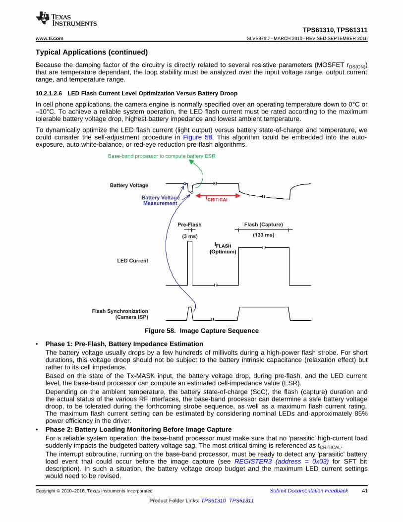
I
(Optimum)FLASH
~ ~~ ~
~ ~
~ ~
~ ~
Battery VoltageMeasurement
Base-band processor to compute battery ESR
tCRITICAL
Flash (Capture)
(133 ms)
Pre-Flash
(3 ms)
Battery Voltage
LED Current
Flash Synchronization(Camera ISP)
41
TPS61310, TPS61311www.ti.com SLVS978D –MARCH 2010–REVISED SEPTEMBER 2016
Product Folder Links: TPS61310 TPS61311
Submit Documentation FeedbackCopyright © 2010–2016, Texas Instruments Incorporated
Typical Applications (continued)Because the damping factor of the circuitry is directly related to several resistive parameters (MOSFET rDS(ON))that are temperature dependant, the loop stability must be analyzed over the input voltage range, output currentrange, and temperature range.
10.2.1.2.6 LED Flash Current Level Optimization Versus Battery Droop
In cell phone applications, the camera engine is normally specified over an operating temperature down to 0°C or–10°C. To achieve a reliable system operation, the LED flash current must be rated according to the maximumtolerable battery voltage drop, highest battery impedance and lowest ambient temperature.
To dynamically optimize the LED flash current (light output) versus battery state-of-charge and temperature, wecould consider the self-adjustment procedure in Figure 58. This algorithm could be embedded into the auto-exposure, auto white-balance, or red-eye reduction pre-flash algorithms.
Figure 58. Image Capture Sequence
• Phase 1: Pre-Flash, Battery Impedance EstimationThe battery voltage usually drops by a few hundreds of millivolts during a high-power flash strobe. For shortdurations, this voltage droop should not be subject to the battery intrinsic capacitance (relaxation effect) butrather to its cell impedance.Based on the state of the Tx-MASK input, the battery voltage drop, during pre-flash, and the LED currentlevel, the base-band processor can compute an estimated cell-impedance value (ESR).Depending on the ambient temperature, the battery state-of-charge (SoC), the flash (capture) duration andthe actual status of the various RF interfaces, the base-band processor can determine a safe battery voltagedroop, to be tolerated during the forthcoming strobe sequence, as well as a maximum flash current rating.The maximum flash current setting can be estimated by considering nominal LEDs and approximately 85%power efficiency in the driver.
• Phase 2: Battery Loading Monitoring Before Image CaptureFor a reliable system operation, the base-band processor must make sure that no 'parasitic' high-current loadsuddenly impacts the budgeted battery voltage sag. The most critical timing is referenced as tCRITICAL.The interrupt subroutine, running on the base-band processor, must be ready to detect any 'parasitic' batteryload event that could occur before the image capture (see REGISTER3 (address = 0x03) for SFT bitdescription). In such a situation, the battery voltage droop budget and the maximum LED current settingswould need to be revised.

t - Time = 500 µs/div
Tx-MASK(2V/div)
I
(200mA/div)LED2
V = 3.6V, V = 4.95V, I = 1750mAIN OUT LIM
DCLC2[2:0] = 000FC2[5:0] = 011000
STRB0(2V/div)
I +
(200mA/div)LED1 ILED3
DCLC13[2:0] = 000FC13[4:0] = 01100
t - Time = 1 ms/div
I
(500mA/div)LED2
V = 3.6V, V = 4.95V, I = 1750mAIN OUT LIM
LED2 Channel OnlyDCLC2[2:0] = 000FC2[5:0] = 100000
STRB0(2V/div)
LED2 Pin Headroom Voltage(1V/div)
V
(1V/div - 3.6V Offset)OUT
42
TPS61310, TPS61311SLVS978D –MARCH 2010–REVISED SEPTEMBER 2016 www.ti.com
Product Folder Links: TPS61310 TPS61311
Submit Documentation Feedback Copyright © 2010–2016, Texas Instruments Incorporated
Typical Applications (continued)
Figure 59. 900-mAh, Li-Ion Battery Transient Response vs SoC and Temperature
10.2.1.3 Application Curves
STRB1 = 0
Figure 60. Flash Sequence
STRB1 = 0
Figure 61. Tx-Masking Operation

t - Time = 2 s/divm
SW(5V/div)
I
(200mA/div)L
V
(100mV/div - 4.95V Offset)OUT
V = 3.6V,IN V = 4.95V
I = 50mA, I = 1750mAOUT
OUT LIM
PFM/PWM OperationENPSM bit = 1
t - Time = 200 µs/div
MODE_CTRL[1:0] = 01DC Light Turn-On
I
(50mA/div)LED2
I
(200mA/div)L
V = 3.6V, V = 4.95V
I = 1750mAIN OUT
LIM
LED2 Channel OnlyDCLC2[2:0] = 100
V
(2V/div)OUT
t - Time = 125 ns/div
SW(2V/div)
I
(200mA/div)L
V
(20mV/div - 4.95V Offset)OUT
V = 3.6V,IN V = 4.95V
I = 300mA, I = 1750mAOUT
OUT LIM
Forced PWM OperationENPSM bit = 0
I
(20 mA/div)LED2
t - Time = 10 µs/div
Frequency = 30 kHzDuty Cycle = 23 %
t - Time = 5 µs/div
Tx-MASK(2V/div)
I
(200mA/div)LED2
I
(200mA/div)L
V = 3.6V, V = 4.95V
I = 1750mAIN OUT
LIM
LED2 Channel OnlyDCLC2[2:0] = 111FC2[5:0] = 100000
t - Time = 100 µs/div
Tx-MASK(2V/div)
I
(200mA/div)LED2
I
(500mA/div)L
V = 3.6V, V = 4.95V
I = 1750mAIN OUT
LIM
LED2 Channel OnlyDCLC2[2:0] = 010FC2[5:0] = 100000
43
TPS61310, TPS61311www.ti.com SLVS978D –MARCH 2010–REVISED SEPTEMBER 2016
Product Folder Links: TPS61310 TPS61311
Submit Documentation FeedbackCopyright © 2010–2016, Texas Instruments Incorporated
Typical Applications (continued)
STRB1 = 0
Figure 62. Tx-Masking Operation
STRB1 = 0
Figure 63. Tx-Masking Operation
Figure 64. Low-Light Dimming Mode Operation Figure 65. PWM Operation
Figure 66. PFM Operation Figure 67. Start-Up Into Video Light Operation

CAMERA ENGINEFLASH SYNCHRONIZATION
RF PA TX ACTIVE
VOUT
AVIN
SW
CI
SW
LED 1
CO
10 mF
PGND
PGND
AGND
L
2.2 mH
SDA
SCL
TPS 61310
LED 2
LED 3
D 12 .5 V .. 5 .5 V
STRB0
STRB1
TS GPIO/PG
INDLED
Privacy
Indicator
I2
C I /F
NRESET
220 k
NTC
Tx -MASK
HARDWARE RESET
Copyright © 2016, Texas Instruments Incorporated
44
TPS61310, TPS61311SLVS978D –MARCH 2010–REVISED SEPTEMBER 2016 www.ti.com
Product Folder Links: TPS61310 TPS61311
Submit Documentation Feedback Copyright © 2010–2016, Texas Instruments Incorporated
Typical Applications (continued)10.2.2 1200-mA High Power White LED Solution Featuring Voltage Mode
Figure 68. 1200-mA High Power White LED Solution Featuring Voltage Mode
10.2.2.1 Design RequirementsTPS6131x operates in standard voltage-boost regulator by setting mode-control bit MODE_CTRL[1:0] = 11. TheLED current sink is turned off in this mode, with VIN = 2.5 V to 5.5 V, VOUT = 4.95 V, operating frequency 2 MHz.
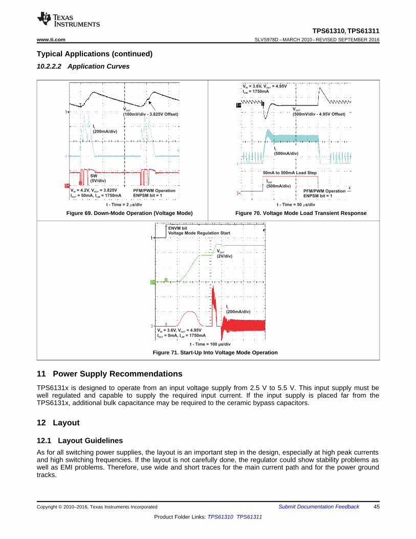
t - Time = 100 µs/div
ENVM bitVoltage Mode Regulation Start
I
(200mA/div)L
V = 3.6V, V = 4.95V
I = 1750mAIN OUT
LIMI = 0mA,OUT
V
(2V/div)OUT
t - Time = 2 s/divm
SW(5V/div)
I
(200mA/div)L
V
(100mV/div - 3.825V Offset)OUT
V = 4.2V,IN V = 3.825V
I = 50mA, I = 1750mAOUT
OUT LIM
PFM/PWM OperationENPSM bit = 1
t - Time = 50 s/divm
I
(500mA/div)L
V
(500mV/div - 4.95V Offset)OUT
V = 3.6V,IN V = 4.95V
I = 1750mAOUT
LIM
PFM/PWM OperationENPSM bit = 1
I
(500mA/div)OUT
50mA to 500mA Load Step
45
TPS61310, TPS61311www.ti.com SLVS978D –MARCH 2010–REVISED SEPTEMBER 2016
Product Folder Links: TPS61310 TPS61311
Submit Documentation FeedbackCopyright © 2010–2016, Texas Instruments Incorporated
Typical Applications (continued)10.2.2.2 Application Curves
Figure 69. Down-Mode Operation (Voltage Mode) Figure 70. Voltage Mode Load Transient Response
Figure 71. Start-Up Into Voltage Mode Operation
11 Power Supply RecommendationsTPS6131x is designed to operate from an input voltage supply from 2.5 V to 5.5 V. This input supply must bewell regulated and capable to supply the required input current. If the input supply is placed far from theTPS6131x, additional bulk capacitance may be required to the ceramic bypass capacitors.
12 Layout
12.1 Layout GuidelinesAs for all switching power supplies, the layout is an important step in the design, especially at high peak currentsand high switching frequencies. If the layout is not carefully done, the regulator could show stability problems aswell as EMI problems. Therefore, use wide and short traces for the main current path and for the power groundtracks.
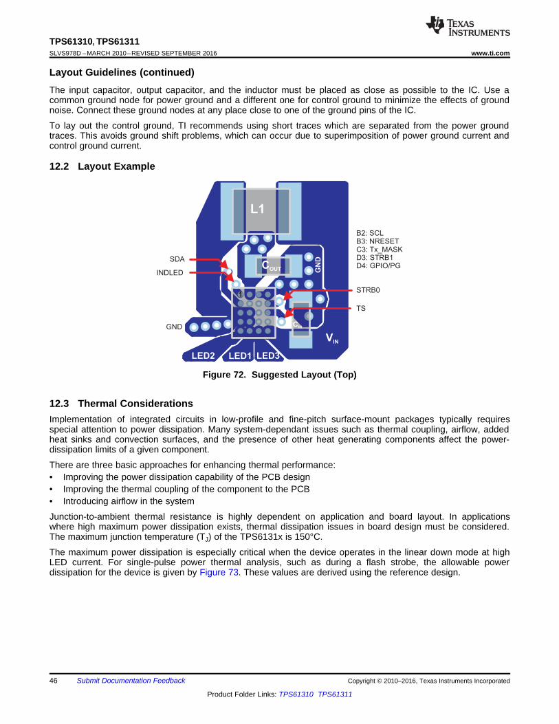
GND
LED1LED2 LED3
VIN
GN
D
L1
COUT
CIN
1
INDLED
SDA
STRB0
TS
B2: SCLB3: NRESETC3: Tx_MASKD3: STRB1D4: GPIO/PG
46
TPS61310, TPS61311SLVS978D –MARCH 2010–REVISED SEPTEMBER 2016 www.ti.com
Product Folder Links: TPS61310 TPS61311
Submit Documentation Feedback Copyright © 2010–2016, Texas Instruments Incorporated
Layout Guidelines (continued)The input capacitor, output capacitor, and the inductor must be placed as close as possible to the IC. Use acommon ground node for power ground and a different one for control ground to minimize the effects of groundnoise. Connect these ground nodes at any place close to one of the ground pins of the IC.
To lay out the control ground, TI recommends using short traces which are separated from the power groundtraces. This avoids ground shift problems, which can occur due to superimposition of power ground current andcontrol ground current.
12.2 Layout Example
Figure 72. Suggested Layout (Top)
12.3 Thermal ConsiderationsImplementation of integrated circuits in low-profile and fine-pitch surface-mount packages typically requiresspecial attention to power dissipation. Many system-dependant issues such as thermal coupling, airflow, addedheat sinks and convection surfaces, and the presence of other heat generating components affect the power-dissipation limits of a given component.
There are three basic approaches for enhancing thermal performance:• Improving the power dissipation capability of the PCB design• Improving the thermal coupling of the component to the PCB• Introducing airflow in the system
Junction-to-ambient thermal resistance is highly dependent on application and board layout. In applicationswhere high maximum power dissipation exists, thermal dissipation issues in board design must be considered.The maximum junction temperature (TJ) of the TPS6131x is 150°C.
The maximum power dissipation is especially critical when the device operates in the linear down mode at highLED current. For single-pulse power thermal analysis, such as during a flash strobe, the allowable powerdissipation for the device is given by Figure 73. These values are derived using the reference design.

0
1
2
3
4
5
6
7
8
9
10
0 20 40 60 80 100 120 140 160 180 200
Pulse Width - ms
P-
Sin
gle
Pu
lse C
on
sta
nt
Po
wer
Dis
sip
ati
on
- W
DIS
T = 65°C riseJ
T = 40°C riseJ
No Airflow
47
TPS61310, TPS61311www.ti.com SLVS978D –MARCH 2010–REVISED SEPTEMBER 2016
Product Folder Links: TPS61310 TPS61311
Submit Documentation FeedbackCopyright © 2010–2016, Texas Instruments Incorporated
Thermal Considerations (continued)
Figure 73. Single Pulse Power Capability

48
TPS61310, TPS61311SLVS978D –MARCH 2010–REVISED SEPTEMBER 2016 www.ti.com
Product Folder Links: TPS61310 TPS61311
Submit Documentation Feedback Copyright © 2010–2016, Texas Instruments Incorporated
13 Device and Documentation Support
13.1 Documentation Support
13.1.1 Related DocumentationFor related documentation see the following:
UM10204, I2C-Bus Specification and User Manual; (Rev. 6, April 2014),http://www.nxp.com/documents/user_manual/UM10204.pdf
13.2 Related LinksThe table below lists quick access links. Categories include technical documents, support and communityresources, tools and software, and quick access to sample or buy.
Table 18. Related Links
PARTS PRODUCT FOLDER SAMPLE & BUY TECHNICALDOCUMENTS
TOOLS &SOFTWARE
SUPPORT &COMMUNITY
TPS61310 Click here Click here Click here Click here Click hereTPS61311 Click here Click here Click here Click here Click here
13.3 Receiving Notification of Documentation UpdatesTo receive notification of documentation updates, navigate to the device product folder on ti.com. In the upperright corner, click on Alert me to register and receive a weekly digest of any product information that haschanged. For change details, review the revision history included in any revised document.
13.4 Community ResourcesThe following links connect to TI community resources. Linked contents are provided "AS IS" by the respectivecontributors. They do not constitute TI specifications and do not necessarily reflect TI's views; see TI's Terms ofUse.
TI E2E™ Online Community TI's Engineer-to-Engineer (E2E) Community. Created to foster collaborationamong engineers. At e2e.ti.com, you can ask questions, share knowledge, explore ideas and helpsolve problems with fellow engineers.
Design Support TI's Design Support Quickly find helpful E2E forums along with design support tools andcontact information for technical support.
13.5 TrademarksNanoFree, E2E are trademarks of Texas Instruments.I2C is a trademark of NXP Semiconductors.All other trademarks are the property of their respective owners.
13.6 Electrostatic Discharge CautionThese devices have limited built-in ESD protection. The leads should be shorted together or the device placed in conductive foamduring storage or handling to prevent electrostatic damage to the MOS gates.
13.7 GlossarySLYZ022 — TI Glossary.
This glossary lists and explains terms, acronyms, and definitions.
14 Mechanical, Packaging, and Orderable InformationThe following pages include mechanical, packaging, and orderable information. This information is the mostcurrent data available for the designated devices. This data is subject to change without notice and revision ofthis document. For browser-based versions of this data sheet, refer to the left-hand navigation.
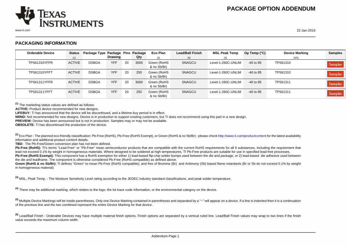
PACKAGE OPTION ADDENDUM
www.ti.com 22-Jan-2016
Addendum-Page 1
PACKAGING INFORMATION
Orderable Device Status(1)
Package Type PackageDrawing
Pins PackageQty
Eco Plan(2)
Lead/Ball Finish(6)
MSL Peak Temp(3)
Op Temp (°C) Device Marking(4/5)
Samples
TPS61310YFFR ACTIVE DSBGA YFF 20 3000 Green (RoHS& no Sb/Br)
SNAGCU Level-1-260C-UNLIM -40 to 85 TPS61310
TPS61310YFFT ACTIVE DSBGA YFF 20 250 Green (RoHS& no Sb/Br)
SNAGCU Level-1-260C-UNLIM -40 to 85 TPS61310
TPS61311YFFR ACTIVE DSBGA YFF 20 3000 Green (RoHS& no Sb/Br)
SNAGCU Level-1-260C-UNLIM -40 to 85 TPS61311
TPS61311YFFT ACTIVE DSBGA YFF 20 250 Green (RoHS& no Sb/Br)
SNAGCU Level-1-260C-UNLIM -40 to 85 TPS61311
(1) The marketing status values are defined as follows:ACTIVE: Product device recommended for new designs.LIFEBUY: TI has announced that the device will be discontinued, and a lifetime-buy period is in effect.NRND: Not recommended for new designs. Device is in production to support existing customers, but TI does not recommend using this part in a new design.PREVIEW: Device has been announced but is not in production. Samples may or may not be available.OBSOLETE: TI has discontinued the production of the device.
(2) Eco Plan - The planned eco-friendly classification: Pb-Free (RoHS), Pb-Free (RoHS Exempt), or Green (RoHS & no Sb/Br) - please check http://www.ti.com/productcontent for the latest availabilityinformation and additional product content details.TBD: The Pb-Free/Green conversion plan has not been defined.Pb-Free (RoHS): TI's terms "Lead-Free" or "Pb-Free" mean semiconductor products that are compatible with the current RoHS requirements for all 6 substances, including the requirement thatlead not exceed 0.1% by weight in homogeneous materials. Where designed to be soldered at high temperatures, TI Pb-Free products are suitable for use in specified lead-free processes.Pb-Free (RoHS Exempt): This component has a RoHS exemption for either 1) lead-based flip-chip solder bumps used between the die and package, or 2) lead-based die adhesive used betweenthe die and leadframe. The component is otherwise considered Pb-Free (RoHS compatible) as defined above.Green (RoHS & no Sb/Br): TI defines "Green" to mean Pb-Free (RoHS compatible), and free of Bromine (Br) and Antimony (Sb) based flame retardants (Br or Sb do not exceed 0.1% by weightin homogeneous material)
(3) MSL, Peak Temp. - The Moisture Sensitivity Level rating according to the JEDEC industry standard classifications, and peak solder temperature.
(4) There may be additional marking, which relates to the logo, the lot trace code information, or the environmental category on the device.
(5) Multiple Device Markings will be inside parentheses. Only one Device Marking contained in parentheses and separated by a "~" will appear on a device. If a line is indented then it is a continuationof the previous line and the two combined represent the entire Device Marking for that device.
(6) Lead/Ball Finish - Orderable Devices may have multiple material finish options. Finish options are separated by a vertical ruled line. Lead/Ball Finish values may wrap to two lines if the finishvalue exceeds the maximum column width.

PACKAGE OPTION ADDENDUM
www.ti.com 22-Jan-2016
Addendum-Page 2
Important Information and Disclaimer:The information provided on this page represents TI's knowledge and belief as of the date that it is provided. TI bases its knowledge and belief on informationprovided by third parties, and makes no representation or warranty as to the accuracy of such information. Efforts are underway to better integrate information from third parties. TI has taken andcontinues to take reasonable steps to provide representative and accurate information but may not have conducted destructive testing or chemical analysis on incoming materials and chemicals.TI and TI suppliers consider certain information to be proprietary, and thus CAS numbers and other limited information may not be available for release.
In no event shall TI's liability arising out of such information exceed the total purchase price of the TI part(s) at issue in this document sold by TI to Customer on an annual basis.

TAPE AND REEL INFORMATION
*All dimensions are nominal
Device PackageType
PackageDrawing
Pins SPQ ReelDiameter
(mm)
ReelWidth
W1 (mm)
A0(mm)
B0(mm)
K0(mm)
P1(mm)
W(mm)
Pin1Quadrant
TPS61310YFFT DSBGA YFF 20 250 178.0 9.2 2.2 2.35 0.8 4.0 8.0 Q1
TPS61310YFFT DSBGA YFF 20 250 180.0 8.4 2.2 2.35 0.8 4.0 8.0 Q1
TPS61311YFFR DSBGA YFF 20 3000 180.0 8.4 2.2 2.35 0.8 4.0 8.0 Q1
TPS61311YFFR DSBGA YFF 20 3000 178.0 9.2 2.2 2.35 0.8 4.0 8.0 Q1
TPS61311YFFT DSBGA YFF 20 250 180.0 8.4 2.2 2.35 0.8 4.0 8.0 Q1
TPS61311YFFT DSBGA YFF 20 250 178.0 9.2 2.2 2.35 0.8 4.0 8.0 Q1
PACKAGE MATERIALS INFORMATION
www.ti.com 26-Jul-2016
Pack Materials-Page 1

*All dimensions are nominal
Device Package Type Package Drawing Pins SPQ Length (mm) Width (mm) Height (mm)
TPS61310YFFT DSBGA YFF 20 250 220.0 220.0 35.0
TPS61310YFFT DSBGA YFF 20 250 182.0 182.0 20.0
TPS61311YFFR DSBGA YFF 20 3000 182.0 182.0 20.0
TPS61311YFFR DSBGA YFF 20 3000 220.0 220.0 35.0
TPS61311YFFT DSBGA YFF 20 250 182.0 182.0 20.0
TPS61311YFFT DSBGA YFF 20 250 220.0 220.0 35.0
PACKAGE MATERIALS INFORMATION
www.ti.com 26-Jul-2016
Pack Materials-Page 2
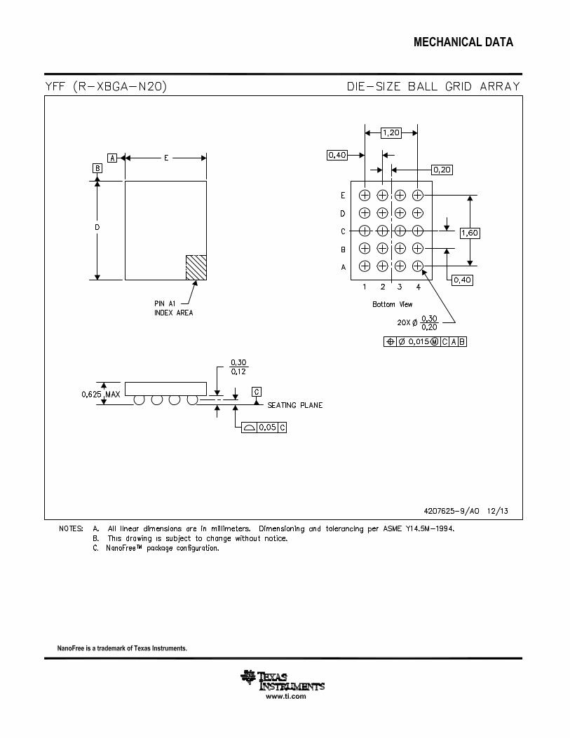

IMPORTANT NOTICE
Texas Instruments Incorporated and its subsidiaries (TI) reserve the right to make corrections, enhancements, improvements and otherchanges to its semiconductor products and services per JESD46, latest issue, and to discontinue any product or service per JESD48, latestissue. Buyers should obtain the latest relevant information before placing orders and should verify that such information is current andcomplete. All semiconductor products (also referred to herein as “components”) are sold subject to TI’s terms and conditions of salesupplied at the time of order acknowledgment.TI warrants performance of its components to the specifications applicable at the time of sale, in accordance with the warranty in TI’s termsand conditions of sale of semiconductor products. Testing and other quality control techniques are used to the extent TI deems necessaryto support this warranty. Except where mandated by applicable law, testing of all parameters of each component is not necessarilyperformed.TI assumes no liability for applications assistance or the design of Buyers’ products. Buyers are responsible for their products andapplications using TI components. To minimize the risks associated with Buyers’ products and applications, Buyers should provideadequate design and operating safeguards.TI does not warrant or represent that any license, either express or implied, is granted under any patent right, copyright, mask work right, orother intellectual property right relating to any combination, machine, or process in which TI components or services are used. Informationpublished by TI regarding third-party products or services does not constitute a license to use such products or services or a warranty orendorsement thereof. Use of such information may require a license from a third party under the patents or other intellectual property of thethird party, or a license from TI under the patents or other intellectual property of TI.Reproduction of significant portions of TI information in TI data books or data sheets is permissible only if reproduction is without alterationand is accompanied by all associated warranties, conditions, limitations, and notices. TI is not responsible or liable for such altereddocumentation. Information of third parties may be subject to additional restrictions.Resale of TI components or services with statements different from or beyond the parameters stated by TI for that component or servicevoids all express and any implied warranties for the associated TI component or service and is an unfair and deceptive business practice.TI is not responsible or liable for any such statements.Buyer acknowledges and agrees that it is solely responsible for compliance with all legal, regulatory and safety-related requirementsconcerning its products, and any use of TI components in its applications, notwithstanding any applications-related information or supportthat may be provided by TI. Buyer represents and agrees that it has all the necessary expertise to create and implement safeguards whichanticipate dangerous consequences of failures, monitor failures and their consequences, lessen the likelihood of failures that might causeharm and take appropriate remedial actions. Buyer will fully indemnify TI and its representatives against any damages arising out of the useof any TI components in safety-critical applications.In some cases, TI components may be promoted specifically to facilitate safety-related applications. With such components, TI’s goal is tohelp enable customers to design and create their own end-product solutions that meet applicable functional safety standards andrequirements. Nonetheless, such components are subject to these terms.No TI components are authorized for use in FDA Class III (or similar life-critical medical equipment) unless authorized officers of the partieshave executed a special agreement specifically governing such use.Only those TI components which TI has specifically designated as military grade or “enhanced plastic” are designed and intended for use inmilitary/aerospace applications or environments. Buyer acknowledges and agrees that any military or aerospace use of TI componentswhich have not been so designated is solely at the Buyer's risk, and that Buyer is solely responsible for compliance with all legal andregulatory requirements in connection with such use.TI has specifically designated certain components as meeting ISO/TS16949 requirements, mainly for automotive use. In any case of use ofnon-designated products, TI will not be responsible for any failure to meet ISO/TS16949.
Products ApplicationsAudio www.ti.com/audio Automotive and Transportation www.ti.com/automotiveAmplifiers amplifier.ti.com Communications and Telecom www.ti.com/communicationsData Converters dataconverter.ti.com Computers and Peripherals www.ti.com/computersDLP® Products www.dlp.com Consumer Electronics www.ti.com/consumer-appsDSP dsp.ti.com Energy and Lighting www.ti.com/energyClocks and Timers www.ti.com/clocks Industrial www.ti.com/industrialInterface interface.ti.com Medical www.ti.com/medicalLogic logic.ti.com Security www.ti.com/securityPower Mgmt power.ti.com Space, Avionics and Defense www.ti.com/space-avionics-defenseMicrocontrollers microcontroller.ti.com Video and Imaging www.ti.com/videoRFID www.ti-rfid.comOMAP Applications Processors www.ti.com/omap TI E2E Community e2e.ti.comWireless Connectivity www.ti.com/wirelessconnectivity
Mailing Address: Texas Instruments, Post Office Box 655303, Dallas, Texas 75265Copyright © 2016, Texas Instruments Incorporated