tps65235-1 lnb voltage regulator with i2c interface ... · tps65235-1 lnb voltage regulator with...
TRANSCRIPT

110 k
1 PF1 PF
10 PH
10 PF
VIN
VOUT
100 nF
PGND
LX
AGND
BOOST
VINVCC
ISET
TCAP
VCP
VLNB
22 nF
2 × 22 PF
0.1 PF
TPS65235-1
Copyright © 2017, Texas Instruments Incorporated
Product
Folder
Order
Now
Technical
Documents
Tools &
Software
Support &Community
An IMPORTANT NOTICE at the end of this data sheet addresses availability, warranty, changes, use in safety-critical applications,intellectual property matters and other important disclaimers. PRODUCTION DATA.
TPS65235-1SLVSDP1A –JANUARY 2017–REVISED DECEMBER 2017
TPS65235-1 LNB Voltage Regulator With I2C Interface
1
1 Features1• Complete Integrate Solution for LNB and I2C
Interface• DiSEqC 2.x, and DiSEqC 1.x Compatible• Supports 5-V, 12-V, and 15-V Power Rail• Up to 1000-mA Accurate Output Current Limit
Adjustable by External Resistor• Boost Switch Peak Current Limit Proportional to
LDO Current Limit• Boost Converter With 140-mΩ Low Rds(on) Internal
Power Switch• Boost Switching Frequency 1-MHz or 500-kHz
Selectable• Audible Noise Avoided at Force PWM Mode• Dedicated Enable Pin for Non-I2C Application• Low-Dropout (LDO) Regulator With Push-Pull
Output Stage for VLNB Output• Built-In Accurate 22-kHz Tone Generator and
External Tone Input Support• Supports Both External 44-kHz and 22-kHz Tone
Input• Adjustable Soft-start and 13-V to 18-V Voltage
Transition Time• 650-mV to 750-mV 22-kHz Tone Amplitude
Selection• I2C Registers Accessible with EN Low• Short Circuit Dynamic Protection• Diagnostics for Output Voltage Level, DiSEqC
Tone Input and Output, Current Level, and CableConnection
• Thermal Protection Available• 20-Pin WQFN 3 mm × 3 mm (RUK) Package
2 Applications• Set Top Box Satellite Receiver• TV Satellite Receiver• PC Card Satellite Receiver• Satellite TV
3 DescriptionDesigned for analog and digital satellite receivers, theTPS65235-1 is a monolithic voltage regulator with I2Cinterface; specifically to provide the 13-V to 18-Vpower supply and the 22-kHz tone signal to the LNBdown converter in the antenna dish or to the multi-switch box. The device offers a complete solutionwith minimum component count, low powerdissipation together with simple design and I2Cstandard interface.
The TPS65235-1 features high power efficiency. Theboost converter integrates a 140-mΩ power MOSFETrunning at 1 MHz or 500 kHz selectable switchingfrequency. Drop out voltage at the linear regulator is0.8 V to minimize power loss. The TPS65235-1provides multiple ways to generate the 22 kHz signal.Integrated linear regulator with push-pull output stagegenerates 22-kHz tone signal superimposed at theoutput even at zero loading. Current limit of linearregulator can be programmed by external resistorwith ±10% accuracy. Full range of diagnostic read byI2C is available for system monitoring.
The TPS65235-1 has a special design at FCCMmode to avoid the audible noise especially when VINis higher or closer to the VLNB output.
The TPS65235-1 supports advanced DiSEqC 2.xstandard with 22-kHz tone detection circuit and outputinterface.
Device Information(1)
PART NUMBER PACKAGE BODY SIZE (NOM)TPS65235-1 WQFN 3.00 mm × 3.00 mm
(1) For all available packages, see the orderable addendum atthe end of the data sheet.
Simplified Schematic

2
TPS65235-1SLVSDP1A –JANUARY 2017–REVISED DECEMBER 2017 www.ti.com
Product Folder Links: TPS65235-1
Submit Documentation Feedback Copyright © 2017, Texas Instruments Incorporated
Table of Contents1 Features .................................................................. 12 Applications ........................................................... 13 Description ............................................................. 14 Revision History..................................................... 25 Pin Configuration and Functions ......................... 36 Specifications......................................................... 4
6.1 Absolute Maximum Ratings ...................................... 46.2 ESD Ratings.............................................................. 46.3 Recommended Operating Conditions....................... 46.4 Thermal Information .................................................. 46.5 Electrical Characteristics........................................... 56.6 Timing Requirements ................................................ 76.7 Typical Characteristics .............................................. 8
7 Detailed Description .............................................. 97.1 Overview ................................................................... 97.2 Functional Block Diagram ......................................... 97.3 Feature Description................................................. 107.4 Device Functional Modes........................................ 18
7.5 Programming........................................................... 197.6 Register Maps ......................................................... 21
8 Application and Implementation ........................ 248.1 Application Information............................................ 248.2 Typical Application .................................................. 24
9 Power Supply Recommendations ...................... 3010 Layout................................................................... 31
10.1 Layout Guidelines ................................................. 3110.2 Layout Example .................................................... 32
11 Device and Documentation Support ................. 3311.1 Device Support .................................................... 3311.2 Documentation Support ....................................... 3311.3 Receiving Notification of Documentation Updates 3311.4 Community Resources.......................................... 3311.5 Trademarks ........................................................... 3311.6 Electrostatic Discharge Caution............................ 3311.7 Glossary ................................................................ 33
12 Mechanical, Packaging, and OrderableInformation ........................................................... 33
4 Revision HistoryNOTE: Page numbers for previous revisions may differ from page numbers in the current version.
Changes from Original (January 2017) to Revision A Page
• Changed the VCP values From: VLNB to 7 V To: –0.3 V to 7 V in the Absolute Maximum Ratings ................................... 4• Changed the GDR values From: VLNB to VCP To: –0.3 V to 7 Vin the Absolute Maximum Ratings .................................. 4• Changed the A(tone) TONEAMP = 0b values From: MIN = 667 TYP = 700 MAX = 746 To: MIN = 617 TYP = 650
MAX = 696 in the Electrical Characteristics ........................................................................................................................... 5• Changed the A(tone) TONEAMP = 1b values From: MIN = 753 TYP = 800 MAX = 853 To: MIN = 703 TYP = 750
MAX = 803 in the Electrical Characteristics ........................................................................................................................... 5
15D
IN1
LX
16VLNB 10 VCTRL
14D
OU
T2
VIN
17VCP 9 ADDR
13E
XT
M3
VC
C
18BOOST 8 FAULT
12S
CL
4A
GN
D
19GDR 7 EN
11S
DA
5T
CA
P
20PGND 6 ISET
Not to scale
Thermal
Pad
3
TPS65235-1www.ti.com SLVSDP1A –JANUARY 2017–REVISED DECEMBER 2017
Product Folder Links: TPS65235-1
Submit Documentation FeedbackCopyright © 2017, Texas Instruments Incorporated
(1) I = input, O = output, I/O = input and output, S = power supply
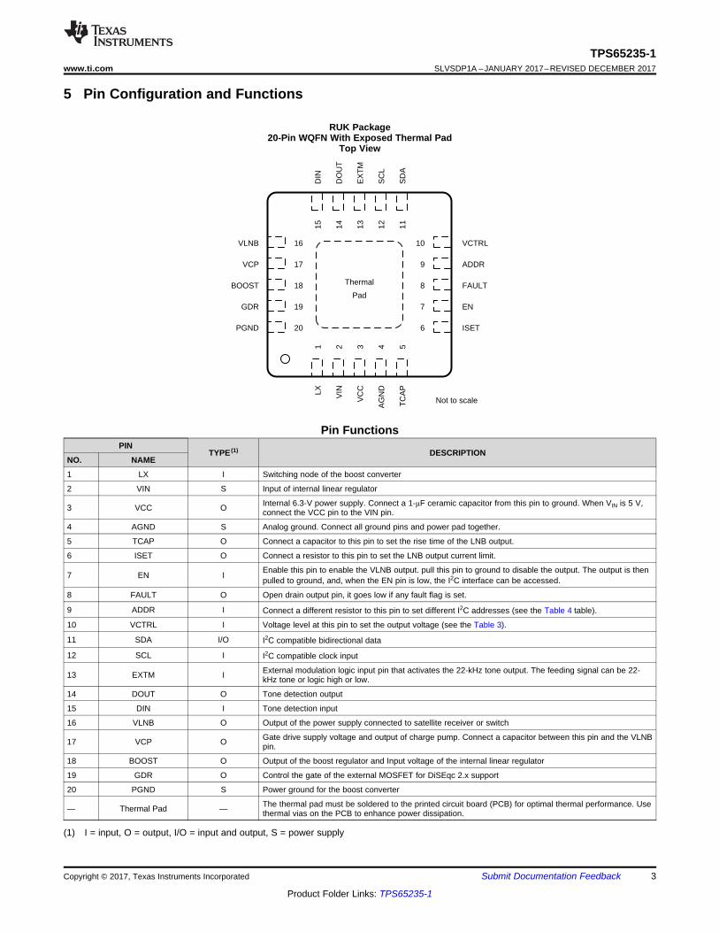
5 Pin Configuration and Functions
RUK Package20-Pin WQFN With Exposed Thermal Pad
Top View
Pin FunctionsPIN
TYPE (1) DESCRIPTIONNO. NAME
1 LX I Switching node of the boost converter
2 VIN S Input of internal linear regulator
3 VCC O Internal 6.3-V power supply. Connect a 1-μF ceramic capacitor from this pin to ground. When VIN is 5 V,connect the VCC pin to the VIN pin.
4 AGND S Analog ground. Connect all ground pins and power pad together.
5 TCAP O Connect a capacitor to this pin to set the rise time of the LNB output.
6 ISET O Connect a resistor to this pin to set the LNB output current limit.
7 EN I Enable this pin to enable the VLNB output. pull this pin to ground to disable the output. The output is thenpulled to ground, and, when the EN pin is low, the I2C interface can be accessed.
8 FAULT O Open drain output pin, it goes low if any fault flag is set.
9 ADDR I Connect a different resistor to this pin to set different I2C addresses (see the Table 4 table).
10 VCTRL I Voltage level at this pin to set the output voltage (see the Table 3).
11 SDA I/O I2C compatible bidirectional data
12 SCL I I2C compatible clock input
13 EXTM I External modulation logic input pin that activates the 22-kHz tone output. The feeding signal can be 22-kHz tone or logic high or low.
14 DOUT O Tone detection output
15 DIN I Tone detection input
16 VLNB O Output of the power supply connected to satellite receiver or switch
17 VCP O Gate drive supply voltage and output of charge pump. Connect a capacitor between this pin and the VLNBpin.
18 BOOST O Output of the boost regulator and Input voltage of the internal linear regulator
19 GDR O Control the gate of the external MOSFET for DiSEqc 2.x support
20 PGND S Power ground for the boost converter
— Thermal Pad — The thermal pad must be soldered to the printed circuit board (PCB) for optimal thermal performance. Usethermal vias on the PCB to enhance power dissipation.

4
TPS65235-1SLVSDP1A –JANUARY 2017–REVISED DECEMBER 2017 www.ti.com
Product Folder Links: TPS65235-1
Submit Documentation Feedback Copyright © 2017, Texas Instruments Incorporated
(1) Stresses beyond those listed under Absolute Maximum Ratings may cause permanent damage to the device. These are stress ratingsonly, which do not imply functional operation of the device at these or any other conditions beyond those indicated under RecommendedOperating Conditions. Exposure to absolute-maximum-rated conditions for extended periods may affect device reliability.
6 Specifications
6.1 Absolute Maximum Ratingsover operating free-air temperature range (unless otherwise noted) (1)
MIN MAX UNIT
Voltage
VIN, LX, BOOST, VLNB 1 30
V
VCP, GDR (referenced to VLNB pin) –0.3 7VCC, EN, ADDR, FAULT, SCL, SDA, VCTRL, EXTM, DOUT, DIN,TCAP –0.3 7
ISET –0.3 3.6PGND –0.3 0.3
Operating junction temperature, TJ –40 150°C
Storage temperature, Tstg –55 150
(1) JEDEC document JEP155 states that 500-V HBM allows safe manufacturing with a standard ESD control process.(2) JEDEC document JEP157 states that 250-V CDM allows safe manufacturing with a standard ESD control process.
6.2 ESD RatingsVALUE UNIT
V(ESD)Electrostaticdischarge
Human-body model (HBM), per ANSI/ESDA/JEDEC JS-001 (1) ±4000V
Charged-device model (CDM), per JEDEC specification JESD22-C101 (2) ±1500
6.3 Recommended Operating Conditionsover operating free-air temperature range (unless otherwise noted)
MIN NOM MAX UNITVIN Input operating voltage 4.5 20 VTA Operating junction temperature –40 125 °C
(1) For more information about traditional and new thermal metrics, see the Semiconductor and IC Package Thermal Metrics applicationreport.
6.4 Thermal Information
THERMAL METRIC (1)TPS65235-1
UNITRUK (WQFN)20 PINS
RθJA Junction-to-ambient thermal resistance 44.8 °C/WRθJC(top) Junction-to-case (top) thermal resistance 47.3 °C/WRθJB Junction-to-board thermal resistance 16.5 °C/WψJT Junction-to-top characterization parameter 0.5 °C/WψJB Junction-to-board characterization parameter 16.4 °C/WRθJC(bot) Junction-to-case (bottom) thermal resistance 3.6 °C/W

5
TPS65235-1www.ti.com SLVSDP1A –JANUARY 2017–REVISED DECEMBER 2017
Product Folder Links: TPS65235-1
Submit Documentation FeedbackCopyright © 2017, Texas Instruments Incorporated
(1) Specified by design
6.5 Electrical Characteristics–40°C ≤ TJ ≤ 125°C, VIN = 12 V, fSW = 1 MHz (unless otherwise noted)
PARAMETER TEST CONDITIONS MIN TYP MAX UNIT
INPUT SUPPLY
VIN Input voltage range 4.5 12 20 V
IDD(SDN) Shutdown supply current EN = 0b 90 120 150 µA
ILDO(Q) LDO quiescent current EN = 1b, IO = 0 A, VVLNB = 18.2 V 1.5 5 8.5 mA
UVLO VIN undervoltage lockoutVIN rising 4.15 4.3 4.45 V
Hysteresis 280 480 550 mV
OUTPUT VOLTAGE
VOUT Regulated output voltage
V(ctrl) = 1, IO = 500 mA 18 18.2 18.4 V
V(ctrl) = 0, IO = 500 mA 13.25 13.4 13.55 V
SCL = 1b, V(ctrl) = 1, IO = 500 mA (NonI2C) 19.18 19.4 19.62 V
SCL = 1b, V(ctrl) = 0, IO = 500 mA (NonI2C) 14.44 14.6 14.76 V
I(OCP) Output short circuit current limitR(SET) = 200 kΩ, Full temperature 580 650 720 mA
TJ = 25°C 629 650 688 mA
fSW Boost switching frequency f = 1 MHz 977 1060 1134 kHz
I(limitsw)(1) Switching current limit VIN = 12 V, VOUT = 18.2 V, R(SET) = 200
kΩ 3 A
Rds(on)_LS On resistance of low side FET VIN = 12 V 90 140 210 mΩ
V(drop) Linear regulator voltage dropoutIO = 500 mA, TONEAMP = 0b 0.44 0.7 1 V
IO = 500 mA, TONEAMP = 1b 0.55 0.8 1.12 V
I(cable) Cable good detection current threshold VIN = 12 V, VOUT = 13.4 V or 18.2 V 0.9 5 8.8 mA
I(rev) Reverse bias current EN = 1b, VVLNB = 21 V 49 58 65 mA
I(rev_dis) Disabled reverse bias current EN = 0b, VVLNB = 21 V 3.72 4.6 5.63 mA
LOGIC SIGNALS
Enable threshold (V(EN)), high 1.6 V
Enable threshold (V(EN)), low 0.8 V
I(EN) Enable internal pullup currentV(EN) = 1.5 V 5 6 7 µA
V(EN) = 1 V 2 3 4 µA
V(VCTRL_H)VCTRL logic threshold level for high-levelinput voltage 2 V
V(VCTRL_L)VCTRL logic threshold level for low-levelinput voltage 0.8 V
V(EXTM_H)EXTM logic threshold level for high-levelinput voltage 2 V
V(EXTM_L)EXTM logic threshold level for low-levelinput voltage 0.8 V
VOL(FAULT) FAULT output low voltage FAULT open drain, IOL = 1 mA 0.4 V
TONE
f(tone) Tone frequency 22-kHz tone output 20 22 24 kHz
A(tone) Tone amplitude
0 mA ≤ IO ≤ 500 mA, CO = 100 nF,TONEAMP = 0b 617 650 696 mV
0 mA ≤ IO ≤ 500 mA, CO = 100 nF,TONEAMP = 1b 703 750 803 mV
D(tone) Tone duty cycle 45% 50% 55%
f(EXTM) External tone input frequency range22-kHz tone output 17.6 22 26.4 kHz
44-kHz tone output 35.2 44 52.8 kHz

6
TPS65235-1SLVSDP1A –JANUARY 2017–REVISED DECEMBER 2017 www.ti.com
Product Folder Links: TPS65235-1
Submit Documentation Feedback Copyright © 2017, Texas Instruments Incorporated
Electrical Characteristics (continued)–40°C ≤ TJ ≤ 125°C, VIN = 12 V, fSW = 1 MHz (unless otherwise noted)
PARAMETER TEST CONDITIONS MIN TYP MAX UNIT
TONE DETECTION
f(DIN) Tone detector frequency capture range 0.4-VPP sine wave 17.6 22 26.4 kHz
V(DIN) Tone detector input amplitude Sine wave, 22 kHz 0.3 1.5 V
V(DOUT) DOUT output voltage Tone present, Iload = 2 mA 0.4 V
GDR Bypass FET gate voltage, LNBTONE_TRANS = 1b, V(LNB) = 18.2 V 23.11 23.5 24.03 V
TONE_TRANS = 0b, V(LNB) = 18.2 V 18.17 18.2 18.23 V
THERMAL SHUT-DOWN (JUNCTION TEMPERATURE)
T(TRIP) Thermal protection trip point Temperature rising 160 °C
T(HYST) Thermal protection hysteresis 20 °C
I2C READ BACK FAULT STATUS
V(PGOOD) PGOOD trip levels
Feedback voltage UVP low 94% 96% 97.1%
Feedback voltage UVP high 93% 94.5% 95.5%
Feedback voltage OVP high 104% 106.6% 108%
Feedback voltage OVP low 102% 104.6% 106%
T(warn) Temperature warning threshold 125 °C
I2C INTERFACE
VIH SDA,SCL input high voltage 2 V
VIL SDA,SCL input low voltage 0.8 V
II Input current SDA, SCL, 0.4 V ≤ VI ≤ 4.5 V –10 10 µA
VOL SDA output low voltage SDA open drain, IOL = 2 mA 0.4 V
f(SCL) Maximum SCL clock frequency 400 kHz

7
TPS65235-1www.ti.com SLVSDP1A –JANUARY 2017–REVISED DECEMBER 2017
Product Folder Links: TPS65235-1
Submit Documentation FeedbackCopyright © 2017, Texas Instruments Incorporated
6.6 Timing RequirementsMIN NOM MAX UNIT
OUTPUT VOLTAGE
tr, tf 13-V to 18-V transition rising falling time C(TCAP) = 22 nF 2 ms
tON(min) Minimum on time for the Low side FET 75 102 130 ns
TONE
tr(tone) Tone rise time
0 mA ≤ IO ≤ 500 mA, CO = 100 nF,Control Reg1[0] = 0b 11 µs
0 mA ≤ IO ≤ 500 mA, CO = 100 nF,Control Reg1[0] = 1b, and EXTM has44-kHz input
5.5 µs
tf(tone) Tone fall time
0 mA ≤ IO ≤ 500 mA, CO = 100 nF,Control Reg1[0] = 0b 10.8 µs
0 mA ≤ IO ≤ 500 mA, CO = 100 nF,Control Reg1[0] = 1b, and EXTM has44 kHz input
5.4 µs
OVERCURRENT PROTECTION
tON Overcurrent protection ON time TIMER = 0b 2.3 3.75 5.52 ms
tOFF Overcurrent protection OFF time TIMER = 0b 98.5 118 133.5 ms
I2C INTERFACE
tBUFBus free time between a STOP and STARTcondition 1.3 µs
tHD_STA Hold time (repeated) START condition 0.6 µs
tSU_STO Setup time for STOP condition 0.6 µs
tLOW LOW period of the SCL clock 1 µs
tHIGH HIGH period of the SCL clock 0.6 µs
tSU_STA Setup time for a repeated START condition 0.6 µs
tSU_DAT Data setup time 0.1 µs
tHD_DAT Data hold time 0 0.9 µs
tRCL Rise time of SCL signal Capacitance of one bus line (pF) 20 + 0.1 CB 300 ns
tRCL1Rise time of SCL Signal after a Repeated STARTcondition and after an acknowledge BIT Capacitance of one bus line (pF) 20 + 0.1 CB 300 ns
tFCL Fall time of SCL signal Capacitance of one bus line (pF) 20 + 0.1 CB 300 ns
tRDA Rise time of SDA signal Capacitance of one bus line (pF) 20 + 0.1 CB 300 ns
tFDA Fall time of SDA signal Capacitance of one bus line (pF) 20 + 0.1 CB 300 ns
CB Capacitance of one bus line(SCL and SDA) 400 pF

Junction Temperature (qC)
I DD S
hutd
own
Cur
rent
(m
A)
-40 -20 0 20 40 60 80 100 120 140105
110
115
120
125
130
135
D005 Junction Temperature (qC)
I DD C
urre
nt L
imit
(mA
)
-40 -20 0 20 40 60 80 100 120 140620
630
640
650
660
670
680
D006
Output Current (A)
Out
put V
olta
ge (
V)
0 0.1 0.2 0.3 0.4 0.5 0.6 0.7 0.8 0.9 118.1
18.12
18.14
18.16
18.18
18.2
18.22
18.24
18.26
18.28
18.3
D003 Junction Temperature (qC)
I DD Q
uies
ent C
urre
nt (
mA
)
-40 -20 0 20 40 60 80 100 120 1403
3.5
4
4.5
5
5.5
6
6.5
7
D004
Output Current (A)
Effi
cien
cy
0 0.1 0.2 0.3 0.4 0.5 0.6 0.7 0.8 0.9 160%
65%
70%
75%
80%
85%
90%
95%
D001
V(LNB) = 13.4 VV(LNB) = 18.2 V
Output Current (A)
Out
put V
olta
ge (
V)
0 0.1 0.2 0.3 0.4 0.5 0.6 0.7 0.8 0.9 113.35
13.36
13.37
13.38
13.39
13.4
13.41
13.42
13.43
13.44
13.45
D002
8
TPS65235-1SLVSDP1A –JANUARY 2017–REVISED DECEMBER 2017 www.ti.com
Product Folder Links: TPS65235-1
Submit Documentation Feedback Copyright © 2017, Texas Instruments Incorporated
6.7 Typical CharacteristicsTA = 25°C, VIN = 12 V, fSW = 1 MHz, CBoost = (2 × 22 µF / 35 V) (unless otherwise noted)
L = 4.7 µH
Figure 1. Power Efficiency
VVLNB = 13.4 V
Figure 2. Load Regulation
VVLNB =18.2 V
Figure 3. Load Regulation Figure 4. Input Supply Quiescent Current vs JunctionTemperature
Figure 5. Shutdown Current vs Junction Temperature
ILOAD = 650 mA
Figure 6. LNB Current Limit vs Junction Temperature

PWM Controller
Tone Generator
REF_Boost
I2C Interface
EX
TM
REF
REF_Boost
REF_LDO
TCAP
Internal RegulatorVCC
SDA
SCL
Fault Diagnose
OCP
OTP
PGOOD
ISE
T
I2C EN
EN
LX
BOOST
VLNB
VCTRL
Charge Pump VCP
FA
ULT
VIN
EN
AG
ND
Logic
ADDR
GDR
DINTone Det
DO
UT
VLNB
VC
PV
LNB
Tone_AutoTone_Trans
EXTM
PGND
Copyright © 2017, Texas Instruments Incorporated
9
TPS65235-1www.ti.com SLVSDP1A –JANUARY 2017–REVISED DECEMBER 2017
Product Folder Links: TPS65235-1
Submit Documentation FeedbackCopyright © 2017, Texas Instruments Incorporated
7 Detailed Description
7.1 OverviewThe TPS65235-1 device is the power management IC (PMIC) that integrates a boost converter, an LDOregulator, and a 22-kHz tone generator to serve as a LNB power supply. This solution compiles the DiSEqC 2.xstandard with or without I2C interface. An external resistor allows for precise programming of the output currentlimit. The 22-kHz tone signal can be generated in one of two ways, either with or without I2C. The integratedboost features low Rds(on) MOSFET and internal compensation. A selectable switching frequency of 1 MHz or 500kHz is designed to reduce the size of passive components and be flexible for design.
The TPS65235-1 device can support the 44-kHz tone output. When the EXTM pin has a 44-kHz tone input, andthe EXTM TONE bit in the Control Register 1 is set to 1b, the LNB tone output is 44 kHz. By default, theTPS65235-1 device has a typical 22-kHz tone output.
7.2 Functional Block Diagram

1.267SET SETR (k ) 117.08 x I (A)�
:
ISET (A)
RS
ET (
K)
0.3 0.4 0.5 0.6 0.7 0.8 0.9 1 1.1 1.2100
150
200
250
300
350
400
450
500
550
D007
y = 117.08x-1.267
10
TPS65235-1SLVSDP1A –JANUARY 2017–REVISED DECEMBER 2017 www.ti.com
Product Folder Links: TPS65235-1
Submit Documentation Feedback Copyright © 2017, Texas Instruments Incorporated
7.3 Feature Description
7.3.1 Boost ConverterThe TPS65235-1 device has an internal compensated boost converter and low-dropout (LDO) linear regulator.The boost converter tracks the LNB output voltage within 800 mV even at loading 1000 mA, which minimizespower loss.
The boost converter operates at 1 MHz by default. The TPS65235-1 device has internal cycle-by-cycle peakcurrent limit in the boost converter and DC current limit in the LNB output to help protect the device from shortcircuits and over loading. When the LNB output is shorted to ground, the LNB output current is clamped at theLDO current limit. The LDO current limit is set by the external resistor at the ISET pin. The current limit of theboost switch is proportional to the LDO current limit. If an overcurrent condition occurs for more than 4 ms, theboost converter enters hiccup mode and retries startup in 128 ms. This hiccup mode ON time and OFF time areselectable through the I2C control register (address 0x01) to be either 4 ms and 128 ms or 8 ms and 256 ms,respectively. At extremely light loads, the boost converter automatically operates in a pulse-skipping mode.
The boost converter is stable with either ceramic capacitor or electrolytic capacitor.
If two or more set-top box LNB outputs are connected together, one output voltage can be set higher than others.The output with the lower set voltage is then effectively turned off. When the voltage drops to the set level, theLNB output with the lower set output voltage returns to normal conditions.
7.3.2 Linear Regulator and Current LimitThe linear regulator is used to generate the 22-kHz tone signal by changing the LDO reference voltage. Thelinear regulator features low-dropout voltage to minimize power loss while maintaining enough head room for the22-kHz tone with 650-mV amplitude. The linear regulator also implements a tight current limit for overcurrentprotection. The current limit is set by an external resistor connected to ISET pin. Figure 7 shows the relationshipbetween the current limit threshold and the resistor value.
Figure 7. Linear Regulator Current Limit Vs Resistor
(1)
A 200-kΩ resistor sets the current to 0.65 A, and 110-kΩ resistor sets the current to approximately 1 A.

. SSTCAP
SS
C (nF)t (ms) 0 8 x
I ( A)
P
SW (OCP)I 5 x I 0.8A �
SW (OCP)I 3 x I 0.8A �
11
TPS65235-1www.ti.com SLVSDP1A –JANUARY 2017–REVISED DECEMBER 2017
Product Folder Links: TPS65235-1
Submit Documentation FeedbackCopyright © 2017, Texas Instruments Incorporated
Feature Description (continued)7.3.3 Boost Converter Current LimitThe boost converter has the cycle-by-cycle peak current limit on the internal Power MOSFET switch to serve asthe secondary protection when LNB output is hard short. With ISW bit default setting 0b on I2C control register0x01, the switch current limit ISW is proportional as LDO current limit I(OCP) set by ISET pin resistor, and therelationship can be expressed as:
(2)
For the 5 V VIN, if LNB current load is up to 1 A, the ISW bit should be written as 1b, the switch current limit ISWfor the internal Power MOSFET is:
(3)
While due to the high power loss at 5 V, VIN, it has a chance to trigger the thermal shutdown before the loading isup to 1 A, especially the VLNB output is high.
7.3.4 Charge PumpThe charge pump circuitry generates a voltage to drive the NMOS of the linear regulator. The voltage across thecharge pump capacitor between VLNB and VCP is about 5.4 V, so the absolute value of the VCP voltage will beVLNB + 5.4 V.
7.3.5 Slew Rate ControlWhen LNB output voltage transits from 13.4 V to 18.2 V or 18.2 V to 13.4 V , the cap at pin TCAP controls thetransition time. This transition time makes sure the boost converter output to follow LNB output change. Usuallyboost converter has low bandwidth and can’t response fast. The voltage at TCAP acts as the reference voltageof the linear regulator. The boost converter’s reference is also based on TCAP with additional fixed voltage togenerate a 0.8 V above the LNB output.
The charging and discharging current is 10 µA, thus the transition time can be estimated as:
(4)
A 22-nF capacitor generates about 2 ms transition time.
In light load conditions, when LNB output voltage is set from 18.2 V to 13.4 V, the voltage drops very slow, whichcauses wrong VOUT_GOOD (Bit 0 at status register 0x02) logic for LNB output voltage detection. TPS65235-1has integrated a pull down circuit to pull down the output during the transition. This ensures the voltage changecan follow the voltage at TCAP. When the 22-kHz tone signal is superimposing on the LNB output voltage, thepull down current can also provide square wave instead of a distorted waveforms.
7.3.6 Short Circuit Protection, Hiccup and Overtemperature ProtectionThe LNB output current limit can be set by an external resistor. When short circuit conditions occur or currentlimit is triggered, the output current is clamped at the current limit for 4 ms with LDO on. If the condition retains,the converter will shut down for 128 ms and then restart. This hiccup behavior prevents IC from being overheat.The hiccup ON/OFF time can be set by I2C register. Refer to Control Register 1 for detail.
The low side MOSFET of the boost converter has a peak current limit threshold which serves as the secondaryprotection. If boost converter’s peak current limit is triggered, the peak current will be clamped as high as 3.8 Awhen setting ISW default and LNB current limit up to 1 A. If loading current continues to increase, output voltagestarts to drop and output power drops.
Thermal shutdown prevents the chip from operating at exceedingly high temperatures. When the junctiontemperature exceeds 160°C, the output shuts down. When the die temperature drops below its lower thresholdtypically 140°C, the output is enabled.

EXTM
TONE
Option 1. Use external tone, gated by EXTM logic pulse
EXTM
TONE
Option 2. Use internal tone, gated by EXTM logic envelop
VLNB(V)
VLNB(V)
12
TPS65235-1SLVSDP1A –JANUARY 2017–REVISED DECEMBER 2017 www.ti.com
Product Folder Links: TPS65235-1
Submit Documentation Feedback Copyright © 2017, Texas Instruments Incorporated
Feature Description (continued)When the chip is in overcurrent protection or thermal shutdown, the I2C interface and logic are still active. TheFAULT pin is pulled down to signal the processor. The FAULT pin signal remains low unless the following actionis taken:1. If I2C interface is not used to control, EN pin must be recycled to pull the FAULT pin back to high.2. If I2C interface is used, the I2C master need to read the status Control Register 2, then the FAULT pin will be
back to high.
7.3.7 Tone GenerationA 22-kHz tone signal is implemented at the LNB output voltage as a carrier for DiSEqC command. This tonesignal can be generated by feeding an external 22-kHz clock at the EXTM pin, and it can also be generated withits internal tone generator controlled by EXTM pin. If EXTM pin is toggled to high, the internal tone signal will besuperimposed at the LNB output, if EXTM pin is low, there will be no tone superimposed at the output stage ofthe regulator facilitates a push-pull circuit, so even at zero loading; the 22-kHz tone at the output is still cleanwithout distortion.
There are two ways to generate the 22-kHz tone signal at the output.
For option1, if the EXTM has 44-kHz tone input, and the bit EXTM TONE of the Control Register 1 is set to 1b,the LNB tone output is 44 kHz.
Figure 8. Two Ways to Generate 22-kHz tone
7.3.8 Tone DetectionA 22-kHz tone detector is implemented in the TPS65235-1 solution. The detector extracts the AC-coupled tonesignal from the DIN input and provides it as an open-drain signal on the DOUT pin. When the DOUTMODE bit inthe Control Register 2 is set to the default setting, if a tone is present, the DOUT output is logic low. If a tone isnot present, the internal output FET is off. If a pullup resistor is connected to the DOUT pin, the output is logichigh. The maximum tone out delay with respect to the input is one and a half of the tone cycle.
The DOUTMODE bit in the Control Register 2 is reserved and should not be used.

INVD 1-
VLNB 0.8
�
OUT IN
peakS
I V x D1I x
1-D 2 L x f �
13
TPS65235-1www.ti.com SLVSDP1A –JANUARY 2017–REVISED DECEMBER 2017
Product Folder Links: TPS65235-1
Submit Documentation FeedbackCopyright © 2017, Texas Instruments Incorporated
Feature Description (continued)7.3.9 Audio Noise RejectionWhen the TPS65235-1 operates in PSM mode, locating the switching frequency at the range of audio frequencyis possible. Which causes audible noise, especially when the VLNB voltage is lower or closer to the VIN voltage,and the current load is light.
When audible noise occurs, setting the TPS65235-1 device to operate in force PWM mode is recommended. Inforce PWM mode, a special design is implemented to avoid the audible noise.
7.3.10 Disable and EnableThe TPS65235-1 device has a dedicated EN pin to disable and enable the LNB output. In a non-I2C application,when the EN pin is pulled high, the LNB output is enabled. When the EN pin is pulled low, the LNB output isdisabled. In an I2C application, when the EN pin is either low or high, the I2C registers can be accessed, whichallows users to change the default LNB output at system power-up. When the I2C_CON bit in the ControlRegister 1 is set to 1b, the LNB output enable or disable is controlled by the EN bit in the Control Register 2. Bydefault, the I2C_CON bit of the control register is set to 0b, which makes the LNB output is controlled by the ENpin. Figure 9 and Figure 10 shows the detailed control behavior.
V(EN) = 0 V I2C_CON = 1b
Figure 9. VLNB Output Controlled by bit EN of ControlRegister 2
I2C_CON = 0b
Figure 10. VLNB Output Controlled by EN Pin
7.3.11 Component Selection
7.3.11.1 Boost InductorThe TPS65235-1 device is recommended to operate with a boost inductor value of 4.7 µH or 10 µH. The boostinductor must be able to support the peak current requirement to maintain the maximum LNB output currentwithout saturation. Use Equation 5 to estimate the peak current of the boost inductor (Ipeak).
where
(6) (6)
With a different inductance, the system has different gain and phase margins. Figure 11 shows a Bode plot ofboost loop with 2 × 10 µF / 35 V of boost capacitor and 4.7 µH, 5.6 µH, 6.8 µH, 8.2 µH, and 10 µH of boostinductance. As the boost inductance increases, the 0-dB crossover frequency keeps relatively constant whilereducing the phase and gain margins. With a 4.7-µH boost inductance, the phase margin is 66.96° and with a10-µH inductance, the phase margin is 39.63°.

10 H, 39.63 degm
4.7 H, 66.96 degm
4.7 Hm
5.6 Hm
6.8 Hm
8.2 Hm
10 Hm
4.7 Hm
5.6 Hm
6.8 Hm
8.2 Hm
10 Hm
Lo
op
Ga
in (
dB
)
14
TPS65235-1SLVSDP1A –JANUARY 2017–REVISED DECEMBER 2017 www.ti.com
Product Folder Links: TPS65235-1
Submit Documentation Feedback Copyright © 2017, Texas Instruments Incorporated
Feature Description (continued)
Figure 11. Gain and Phase Margin of the Boost Loop with Different Inductance(VIN = 12 V, VOUT = 18.2 V, ILOAD = 1 A, fSW = 1 MHz, 5 µF, Typical Bode Plot)
7.3.11.2 Capacitor SelectionThe TPS65235-1 device has a 1-MHz nonsynchronous boost converter integrated and the boost converterfeatures the internal compensation network. The TPS65235-1 device works well with both ceramic capacitor andelectrolytic capacitor.
The recommended ceramic capacitors for the TPS65235-1 application are, at the minimum, rated as X7R/X5R,with a 35-V rating, and a 1206 size for the achieving lower LNB output ripple. Table 1 lists the recommendedceramic capacitors list for both 4.7-µH and 10-µH boost inductors.
If more cost-effictive design is needed, use a 100-µF electrolytic (low ESR) and a 10-µF or 35-V ceramiccapacitor.
Table 1. Boost Inductor and Capacitor SelectionsBOOST INDUCTOR CAPACITORS TOLERANCE (%) RATING (V) SIZE
10 µH2 × 22 µF ±10 35 12062 × 10 µF ±10 35 1206
4.7 µH2 × 22 µF ±10 35 12062 × 10 µF ±10 35 1206
22 µF ±10 35 1206

4 Fm
5 Fm
7.5 Fm
10 Fm
15 Fm
20 Fm
4 Fm
5 Fm
7.5 Fm
10 Fm
15 Fm
20 Fm
4 F, 57.45 degm
20 F, 84.49 degm
4 Fm
20 Fm
Lo
op
Ga
in (
dB
)
15
TPS65235-1www.ti.com SLVSDP1A –JANUARY 2017–REVISED DECEMBER 2017
Product Folder Links: TPS65235-1
Submit Documentation FeedbackCopyright © 2017, Texas Instruments Incorporated
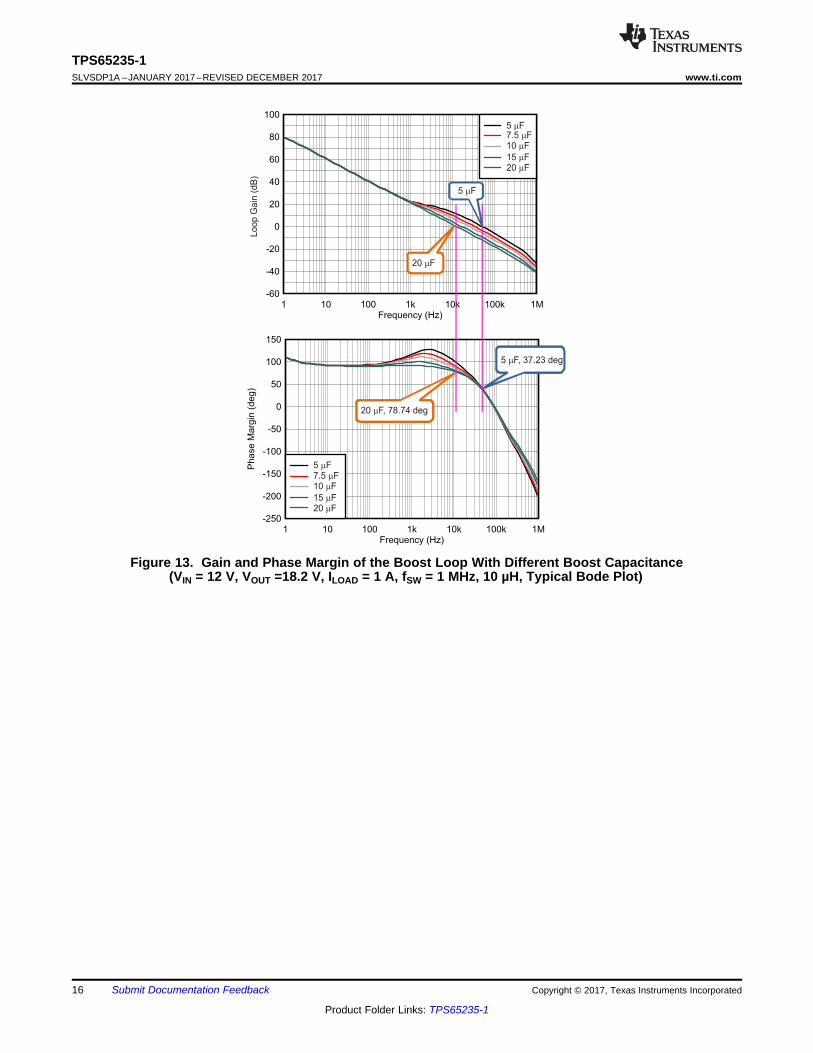
Figure 12 and Figure 13 show a bode plot of boost loop with 4.7-µH and 10-µH inductance and 4 µF, 5 µF, 7.5µF, 10 µF, 15 µF, and 20 µF of boost capacitance after degrading. As the boost capacitance increases, thephase margin increases.
Figure 12. Gain and Phase Margin of the Boost Loop With Different Boost Capacitance(VIN = 12 V, VOUT = 18.2 V, ILOAD = 1 A, fSW = 1 MHz, 4.7 µH, Typical Bode Plot)
5 Fm
7.5 Fm
10 Fm
15 Fm
20 Fm
5 Fm
7.5 Fm
10 Fm
15 Fm
20 Fm
5 F, 37.23 degm
20 F, 78.74 degm
5 Fm
20 Fm
Lo
op
Ga
in (
dB
)
16
TPS65235-1SLVSDP1A –JANUARY 2017–REVISED DECEMBER 2017 www.ti.com
Product Folder Links: TPS65235-1
Submit Documentation Feedback Copyright © 2017, Texas Instruments Incorporated
Figure 13. Gain and Phase Margin of the Boost Loop With Different Boost Capacitance(VIN = 12 V, VOUT =18.2 V, ILOAD = 1 A, fSW = 1 MHz, 10 µH, Typical Bode Plot)

1 µF
10 µH
10 µF
VOUT
100 nF
PGND
GDR
LX
BOOST
VIN
1 2
20
19
18
17
16
VCP
VLNB
2x22 µF
0.1 µF
D0D2
D1
D3
TPS65235-1
VIN
Copyright © 2017, Texas Instruments Incorporated
17
TPS65235-1www.ti.com SLVSDP1A –JANUARY 2017–REVISED DECEMBER 2017
Product Folder Links: TPS65235-1
Submit Documentation FeedbackCopyright © 2017, Texas Instruments Incorporated
(1) See Third-party Products Disclaimer
7.3.11.3 Surge ComponentsIf a surge test is required for the application, the D0 and D2 diodes should be added as the external protectioncomponents. If no surge test is required, remove the D0 and D2 diodes.Table 2 lists the recommended surgecomponents.
Table 2. Surge ComponentsDESIGNATOR DESCRIPTION PART NUMBER MANUFACTURER (1)
D0 Diode, TVS, Uni, 28 V, 1500 W, SMC SMCJ28A Fairchild SemiconductorD2 Diode, Schottky, 40 V, 2 A, SMA B240A-13-F Diodes Inc.
Figure 14. Surge Components Selection
7.3.11.4 Consideration for Boost Filtering and LNB NoiseSmaller capacitance on the BOOST pin reduces the cost of the system. However, when the inductor in system isthe same, the smaller capacitance on the boost and the larger ripple on the LNB output.

18
TPS65235-1SLVSDP1A –JANUARY 2017–REVISED DECEMBER 2017 www.ti.com
Product Folder Links: TPS65235-1
Submit Documentation Feedback Copyright © 2017, Texas Instruments Incorporated
(1) I2C_CON is the bit7 of the I2C control register 0x01, which is used to set the VLNB output controlled by the I2C register or not.(2) When I2C interface is used in design, all the I2C registers are accessible even if the I2C_CON bit is 0b.(3) When I2C_CON is 1b, the VLNB output is controlled by the I2C control register even if the EN pin is low.(4) When I2C interface is used in design, it is recommended to set the I2C_CON with 1b, if not, the LNB output will be variable because the
SCL is toggled by the I2C register access as the clock signal.(5) Bit EN of the control register2 is used to disable or enable the LNB output, by default , the bit EN is 1b which enable the LNB output
7.4 Device Functional ModesTable 3 is the logic table for the device.
Table 3. Logic tableEN I2C_CON (1) (2) (3) SCL VCTRL VLNB (4)
H 0 H H 19.4 VH 0 H L 14.6 VH 0 L H 18.2 VH 0 L L 13.4 V
X 1 X X Controlled by VSET[3:0]bits at 0x01 register (5)
L 0 X X 0 V

tSU, DATtLOW
tHD, DAT
tHIGH
StartCondition
tHD, STA
SCL
tr tf
SDA
tSU, STA
tHD, STA
tSP
tSU, STO
tBUF
Repeated StartCondition
StopCondition
StartCondition
19
TPS65235-1www.ti.com SLVSDP1A –JANUARY 2017–REVISED DECEMBER 2017
Product Folder Links: TPS65235-1
Submit Documentation FeedbackCopyright © 2017, Texas Instruments Incorporated
7.5 Programming
7.5.1 Serial Interface DescriptionI2C is a 2-wire serial interface developed by Philips Semiconductor (see I2C-Bus Specification, Version 2.1,January 2000). The bus consists of a data line (SDA) and a clock line (SCL) with pullup structures. When the busis idle, both SDA and SCL lines are pulled high external. All the I2C compatible devices connect to the I2C busthrough open drain I/O pins, SDA and SCL. A master device, usually a microcontroller (MCU) or a digital signalprocessor (DSP), controls the bus. The master device is responsible for generating the SCL signal and deviceaddresses. The master device also generates specific conditions that indicate the START and STOP of datatransfer. A slave device receives, transmits data, or both on the bus under control of the master device.
The TPS65235-1 device works as a slave and supports the following data transfer modes, as defined in theI2CBus Specification: standard mode (100 kbps), and fast mode (400 kbps). The interface adds flexibility to thepower supply solution, enabling most functions to be programmed to new values depending on the instantaneousapplication requirements. Register contents remain intact as long as supply voltage remains above 4.5 V(typical).
The data transfer protocol for standard and fast modes is exactly the same; therefore, they are referred to asF/S-mode in this document. The TPS65235-1 device supports 7-bit addressing; 10-bit addressing and generalcall address are not supported.
The TPS65235-1 device has a 7-bit address set by ADDR pin. Table 4 shows how to set the I2C address.
Table 4. I2C Address SelectionADDR PIN I2C ADDRESS ADDRESS FORMAT (A6 ≥ A0)
Connect to VCC 0x08 000 1000bFloating 0x09 000 1001bConnected to GND 0x10 001 0000bResistor divider to make ADDR pin voltage in 3 V ~ VCC - 0.8 V 0x11 001 0001b
Figure 15. I2C Interface Timing Diagram

N: Not Acknowledge
A: Acknowledge
S: Start
P: Stop
Sr: Repeated Start
System Host
Chip
S 7-Bit Slave AddressA6«.A0
0 A Register1 Address A Sr 17-Bit Slave Address A
Data Byte N P
S7-Bit Slave Address
A6«.A00 A Register Address A Data Byte A P
20
TPS65235-1SLVSDP1A –JANUARY 2017–REVISED DECEMBER 2017 www.ti.com
Product Folder Links: TPS65235-1
Submit Documentation Feedback Copyright © 2017, Texas Instruments Incorporated
7.5.2 TPS65235-1 I2C Update SequenceThe TPS65235-1 requires a start condition, a valid I2C address, a register address byte, and a data byte for asingle update. After the receipt of each byte, TPS65235-1 device acknowledges by pulling the SDA line lowduring the high period of a single clock pulse. TPS65235-1 performs an update on the falling edge of the LSBbyte.
When the TPS65235-1 is disabled (EN pin tied to ground) the device cannot be updated via the I2C interface.
Figure 16. I2C Write Data Format
Figure 17. I2C Read Data Format

21
TPS65235-1www.ti.com SLVSDP1A –JANUARY 2017–REVISED DECEMBER 2017
Product Folder Links: TPS65235-1
Submit Documentation FeedbackCopyright © 2017, Texas Instruments Incorporated
7.6 Register Maps
7.6.1 Control Register 1 (address = 0x00) [reset = 0x08]
Figure 18. Control Register 1
7 6 5 4 3 2 1 0I2C_CON PWM/PSM RESERVED VSET[3:0] EXTM TONER/W-0b R/W-0b R/W-0b R/W-0100b R/W-0b
Table 5. Control Register 1Bit Field Type Reset Description
7 I2C_CON R/W 0b 0b = I2C control disabled1b = I2C control enabled
6 PWM/PSM R/W 0b 0b = PSM at light load1b = Forced PWM
5 RESERVED R/W 0b Reserved4-1 VSET[3:0]
R/W 0100b
LNB output voltage selection0000b = 11 V0001b = 11.6 V0010b = 12.2 V0011b = 12.8 V0100b = 13.4 V0101b = 14 V0110b = 14.6 V0111b = 15.2 V1000b = 15.8 V1001b = 16.4 V1010b = 17 V1011b = 17.6 V1100b = 18.2 V1101b = 18.8 V1110b = 19.4 V1111b = 20 V
0 EXTM TONE R/W 0b
0b = EXTM 44-kHz tone input not support, with only 22-kHz toneoutput at VLNB1b = EXTM 44-kHz tone input support, with 44-kHz tone outputat VLNB

22
TPS65235-1SLVSDP1A –JANUARY 2017–REVISED DECEMBER 2017 www.ti.com
Product Folder Links: TPS65235-1
Submit Documentation Feedback Copyright © 2017, Texas Instruments Incorporated
7.6.2 Control Register 2 (address = 0x01) [reset = 0x09]
Figure 19. Control Register 2
7 6 5 4 3 2 1 0TONEAMP TIMER ISW FSET EN DOUTMODE TONE_AUTO TONE_TRANS
R/W-0b R/W-0b R/W-0b R/W-0b R/W-1b R/W-0b R/W-0b R/W-1b
Table 6. Control Register 2Bit Field Type Reset Description
7 TONEAMP R/W 0b 0b = 22-kHz tone amplitude is 650 mV (typ)1b = 22-kHz tone amplitude is 750 mV (typ)
6 TIMER R/W 0b 0b = Hiccup ON time set to 4 ms and OFF time set to 128 ms1b = Hiccup ON time set to 8 ms and OFF time set to 256 ms
5 ISWR/W 0b 0b = Boost switch peak current limit set to 3 × IOCP + 0.8 A
1b = Boost switch peak current limit set to 5 × IOCP + 0.8 A4 FSET
R/W 0b 0b = 1-MHz switching frequency1b = 500-kHz switching frequency
3 ENR/W 1b 0b = LNB output disabled
1b = LNB output voltage Enabled2 DOUTMODE
R/W 0b 0b = DOUT is kept to low when DIN has the tone input1b = Reserved, cannot set to 1b
1 TONE_AUTO
R/W 0b
0b = GDR (External bypass FET control) is controlled byTONE_TRANS1b = GDR (External bypass FET control) is automaticallycontrolled by 22-kHz tones transmit
0 TONE_TRANS R/W 1b
0b = GDR output with VLNB voltage for tone receive. BypassFET is OFF for tone receiving from satellite1b = GDR output with VCP voltage. Bypass FET is ON for tonetransmit from TPS65235-1
Table 7. 22-kHz Tone Receive Mode SelectionTONE_AUTO TONE_TRANS BYPASS FET
0b 0b OFF0b 1b ON1b x Auto Detect
The TPS65235-1 has full range of diagnostic flags for operation and debug. Processor can read the statusregister to check the error conditions. Once the error happens, the flags are changed, once the errors are gone,the flags are set back without I2C access.
If the TSD and OCP flags are triggered, FAULT pin will be pulled low, so FAULT pin can be the interrupt signal toprocessor. Once TSD and OCP are set to 1b, the FAULT pin logic is latched to low, processor need to read thisstatus register to release the fault conditions.

23
TPS65235-1www.ti.com SLVSDP1A –JANUARY 2017–REVISED DECEMBER 2017
Product Folder Links: TPS65235-1
Submit Documentation FeedbackCopyright © 2017, Texas Instruments Incorporated
7.6.3 Status Register (address = 0x02) [reset = 0x29]
Figure 20. Status Register
7 6 5 4 3 2 1 0Reserved 0 LDO_ON T125 TSD OCP CABLE_GOOD VOUT_GOOD
R-0b R-0b R-0b R-0b R-1b R-0b R-0b R-1b
Table 8. Status RegisterBit Field Type Reset Description
7 Reserved R 0b Reserved
6 TDETGOOD R 0b 0b = 22-kHz tone detected on DIN pin is out of range1b = 22-kHz tone detected on DIN pin is in range
5 LDO_ONR 1b 0b = Internal LDO is turned off but boost converter is on
1b = Internal LDO is turned on and boost converter is on4 T125
R 0b 0b = Die temperature < 125°C1b = Die temperature > 125°C
3 TSD
R 1b
0b = No thermal shutdown triggered1b = Thermal shutdown triggered. The FAULT pin logic islatched to low, processor need to read this register to releasethe fault conditions
2 OCP
R 0b
0b = Overcurrent protection conditions released1b = Overcurrent protection triggered. The FAULT pin logic islatched to low, processor need to read this register to releasethe fault conditions
1 CABLE_GOODR 0b 0b = Cable not connected
1b = Cable connection good
0 VOUT_GOOD R 1b 0b = LNB output voltage out of range1b = LNB output voltage in range

110 k
1 PF
1 PF
TPS65235-1
SC
L
EX
TM
DO
UT
DIN
PGND
GDR
LX AG
ND
10
BOOST FAULT
VCTRL
ADDR
VIN
VC
C
1 2 3 4
20
19
18
12131415
8
917
16
SD
A
11
ISET
EN
6
7
TC
AP
5
VCP
VLNB
22 nF
10 k
D0
VOUT
100 nF
2 × 22 PF
0.1 PF
1 PF
10 PH
10 PF
VIN
Copyright © 2017, Texas Instruments Incorporated
24
TPS65235-1SLVSDP1A –JANUARY 2017–REVISED DECEMBER 2017 www.ti.com
Product Folder Links: TPS65235-1
Submit Documentation Feedback Copyright © 2017, Texas Instruments Incorporated
8 Application and Implementation
NOTEInformation in the following applications sections is not part of the TI componentspecification, and TI does not warrant its accuracy or completeness. TI’s customers areresponsible for determining suitability of components for their purposes. Customers shouldvalidate and test their design implementation to confirm system functionality.
8.1 Application InformationThe TPS65235 supports both DisEqc1.x and DisEqc2.x application. When the input voltage VIN is greater thanthe expected output voltage VLNB, the linear regulator drops the voltage difference between VIN and VLNB,which causes the lower efficiency and the higher power loss on the internal linear regulator if the current loadingis high. For care must be taken to ensure that the safe operating temperature range of the TPS65235-1 is notexceeded. TI recommends operating the device in force PWM mode when VIN > VOUT to reduce output ripple.
8.2 Typical Application
8.2.1 DiSEqc1.x SupportTPS65235-1 can operate in I2C and non-I2C interface mode. Figure 21 shows the application with the device inI2C interface mode to support DiSEqC 1.x application. In non-I2C mode, the SCL, SDA, and ADDR pins can befloating.
Figure 21. Application for DiSEqc1.x Support
25
TPS65235-1www.ti.com SLVSDP1A –JANUARY 2017–REVISED DECEMBER 2017
Product Folder Links: TPS65235-1
Submit Documentation FeedbackCopyright © 2017, Texas Instruments Incorporated
Typical Application (continued)8.2.1.1 Design RequirementsFor this design example, use the parameters in Table 9.
Table 9. Design ParametersPARAMETER VALUE
Input voltage range, VIN 4.5 V to 20 VOutput voltage range VLNB 11 V to 20 V
Output current range 0 A to 1 A
8.2.1.2 Detailed Design ProcedureTo begin the design process, the following component values must be selected:• Inductor
– Choose the appropriate value of the inductor based on application cost requirements, ripple requirements,and Component Selection.
• BOOST capacitor– Choose the appropriate BOOST capacitor value based on application cost requirements, ripple
requirements, and Component Selection.• Diodes
– The D0 and D2 diodes are used to help meet the surge-protection requirement of the application. If theapplication does not require surge protection, remove these diodes. For diode component selection, referto Surge Components.
– The D1 diode is used for the boost loop. A Schottky diode is recommended for D1. The applicationrequirements, which include input power range, output power range, and the current requirement,determine the current and voltage capability of the D1 diode.
– The D3 diode is to help with the output protection for the VLNB voltage. A Schottky diode is recommendedfor D3. The application requirements determine the current and voltage capability of the D3 diode.
26
TPS65235-1SLVSDP1A –JANUARY 2017–REVISED DECEMBER 2017 www.ti.com
Product Folder Links: TPS65235-1
Submit Documentation Feedback Copyright © 2017, Texas Instruments Incorporated
8.2.1.3 Application CurvesTA = 25°C, VIN = 12 V, fSW = 1 MHz, CBoost = (2 × 22 µF / 35 V) (unless otherwise noted)
VVLNB = 13.4 V
Figure 22. Soft Start, Delay from EN High toLNB Output High
VVLNB = 13.4 V
Figure 23. Disabled, Delay from EN Low toLNB Output Low
VVLNB = 18.2 V
Figure 24. Soft-Start, Delay from EN High toLNB Output High
VVLNB = 18.2 V
Figure 25. Disabled, Delay From EN Low toLNB Output Low
EN = 0b VVLNB =13.4 V
Figure 26. Soft Start, Delay From I2C Enable (I2C_CON =1b) to LNB Output High
EN = 0b VVLNB = 13.4 V
Figure 27. Delay From I2C Disable (I2C_CON = 0b) toLNB Output Low
27
TPS65235-1www.ti.com SLVSDP1A –JANUARY 2017–REVISED DECEMBER 2017
Product Folder Links: TPS65235-1
Submit Documentation FeedbackCopyright © 2017, Texas Instruments Incorporated
VVLNB = 13.4 V
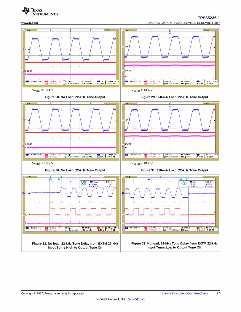
Figure 28. No Load, 22-kHz Tone Output
VVLNB = 13.4 V
Figure 29. 950-mA Load, 22-kHz Tone Output
VVLNB = 18.2 V
Figure 30. No Load, 22-kHz Tone Output
VVLNB = 18.2 V
Figure 31. 950-mA Load, 22-kHz Tone Output
Figure 32. No load, 22-kHz Tone Delay from EXTM 22-kHzInput Turns High to Output Tone On
Figure 33. No load, 22-kHz Tone Delay from EXTM 22-kHzInput Turns Low to Output Tone Off
28
TPS65235-1SLVSDP1A –JANUARY 2017–REVISED DECEMBER 2017 www.ti.com
Product Folder Links: TPS65235-1
Submit Documentation Feedback Copyright © 2017, Texas Instruments Incorporated
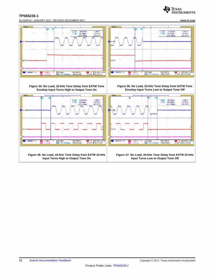
Figure 34. No Load, 22-kHz Tone Delay from EXTM ToneEnvelop Input Turns High to Output Tone On
Figure 35. No Load, 22-kHz Tone Delay from EXTM ToneEnvelop Input Turns Low to Output Tone Off
Figure 36. No Load, 44-kHz Tone Delay from EXTM 22-kHzInput Turns High to Output Tone On
Figure 37. No Load, 44-kHz Tone Delay from EXTM 22-kHzInput Turns Low to Output Tone Off

110 k
1 PF
10 PH
10 PF
VIN
VOUT100 nF
8
9
6
7
22 nF
2 × 22PF
0.1 PF
15
22 nF
220 PH
10 nF10 k
10 k
10 k
D2 D3
D1
TPS65235-1
SC
L
EX
TM
DO
UT
DIN
PGND
GDR
LX AG
ND
10
BOOST FAULT
VCTRL
ADDR
VIN
VC
C
1 2 3 4
20
19
18
12131415
17
16
SD
A
11
ISET
EN
TC
AP
5
VCP
VLNB
1 PF
Copyright © 2017, Texas Instruments Incorporated
29
TPS65235-1www.ti.com SLVSDP1A –JANUARY 2017–REVISED DECEMBER 2017
Product Folder Links: TPS65235-1
Submit Documentation FeedbackCopyright © 2017, Texas Instruments Incorporated
8.2.2 DiSEqc2.x SupportThe TPS65235-1 can support both DiSEqC 1.x application and DiSEqC 2.x application. Figure 38 shows theapplication for supporting DiSEqC 2.x application.
Figure 38. Application Schematic for DiSEqc2.x Support
8.2.2.1 Design RequirementsRefer to the DiSEqc1.x Support section for design requirements.
8.2.2.2 Detailed Design ProcedureRefer to the DiSEqc1.x Support section for detailed design procedures.

30
TPS65235-1SLVSDP1A –JANUARY 2017–REVISED DECEMBER 2017 www.ti.com
Product Folder Links: TPS65235-1
Submit Documentation Feedback Copyright © 2017, Texas Instruments Incorporated
8.2.2.3 Application CurveRefer to the DiSEqc1.x Support section for typical application curves. Figure 39 is the unique tone-detectioncurve for the DiSEqC 2.x application.
Figure 39. DOUT Tone Detection Output
9 Power Supply RecommendationsThe device is designed to operate from an input supply ranging from 4.5 V to 20 V. The input supply should bewell regulated. If the input supply is located more than a few inches from the converter, an additional bulkcapacitance, typically with a value 100 µF, may be required in addition to the ceramic bypass capacitors.

31
TPS65235-1www.ti.com SLVSDP1A –JANUARY 2017–REVISED DECEMBER 2017
Product Folder Links: TPS65235-1
Submit Documentation FeedbackCopyright © 2017, Texas Instruments Incorporated
10 Layout
10.1 Layout GuidelinesThe TPS65235-1 is designed to layout in 2-layer PCB. To ensure reliability of the device, following commonprinted-circuit board layout guidelines is recommended.• It is critical to make sure the ground of input capacitor, output capacitor, and the boost converter are
connected at one point at same layer.• The PGND and AGND pins are located in different regions. Connect these grounds to the thermal pad. Other
components are connected the AGND pin.• Put the BOOST capacitors as close as possible.• The loop from the VIN inductor to the LX pin should be as short as possible.• The loop from the VIN inductor to D1 Schottky diode to the BOOST should be as short as possible.• The loop for boost capacitors to the PGND pin should be within the loop from the LX pin to D1 Schottky diode
to the BOOST pin.

110k
1uF1uF10uH
10uF
VIN
VOUT
100nF
SC
L
EX
TM
DO
UT
DIN
PGND
GDR
LX
AG
ND
10
BOOST FAULT
VCTRL
ADDR
VIN
VC
C
1 2 3 4
20
19
18
12131415
8
917
16
SD
A
11
ISET
EN
6
7
TC
AP
5
VCP
VLNB
22nF
2x22uF
0.1uF
10k
VIA to GND Plane (Inner Layer)
Polygonal Copper Pour
D1
D3
D2
32
TPS65235-1SLVSDP1A –JANUARY 2017–REVISED DECEMBER 2017 www.ti.com
Product Folder Links: TPS65235-1
Submit Documentation Feedback Copyright © 2017, Texas Instruments Incorporated
10.2 Layout Example
Figure 40. Layout

33
TPS65235-1www.ti.com SLVSDP1A –JANUARY 2017–REVISED DECEMBER 2017
Product Folder Links: TPS65235-1
Submit Documentation FeedbackCopyright © 2017, Texas Instruments Incorporated
11 Device and Documentation Support
11.1 Device Support
11.1.1 Third-Party Products DisclaimerTI'S PUBLICATION OF INFORMATION REGARDING THIRD-PARTY PRODUCTS OR SERVICES DOES NOTCONSTITUTE AN ENDORSEMENT REGARDING THE SUITABILITY OF SUCH PRODUCTS OR SERVICESOR A WARRANTY, REPRESENTATION OR ENDORSEMENT OF SUCH PRODUCTS OR SERVICES, EITHERALONE OR IN COMBINATION WITH ANY TI PRODUCT OR SERVICE.
11.2 Documentation Support
11.2.1 Related DocumentationFor related documentation see the following:• Texas Instruments, Evaluation Module for the TPS65235-1 LNB Voltage Regulator With I2C Interface for
DiSEqC2.x Application user's guide• Texas Instruments, Evaluation Module for the TPS65235-1 LNB Voltage Regulator With I2C Interface for
DiSEqC1.x Application user's guide
11.3 Receiving Notification of Documentation UpdatesTo receive notification of documentation updates, navigate to the device product folder on ti.com. In the upperright corner, click on Alert me to register and receive a weekly digest of any product information that haschanged. For change details, review the revision history included in any revised document.
11.4 Community ResourcesThe following links connect to TI community resources. Linked contents are provided "AS IS" by the respectivecontributors. They do not constitute TI specifications and do not necessarily reflect TI's views; see TI's Terms ofUse.
TI E2E™ Online Community TI's Engineer-to-Engineer (E2E) Community. Created to foster collaborationamong engineers. At e2e.ti.com, you can ask questions, share knowledge, explore ideas and helpsolve problems with fellow engineers.
Design Support TI's Design Support Quickly find helpful E2E forums along with design support tools andcontact information for technical support.
11.5 TrademarksE2E is a trademark of Texas Instruments.All other trademarks are the property of their respective owners.
11.6 Electrostatic Discharge CautionThis integrated circuit can be damaged by ESD. Texas Instruments recommends that all integrated circuits be handled withappropriate precautions. Failure to observe proper handling and installation procedures can cause damage.
ESD damage can range from subtle performance degradation to complete device failure. Precision integrated circuits may be moresusceptible to damage because very small parametric changes could cause the device not to meet its published specifications.
11.7 GlossarySLYZ022 — TI Glossary.
This glossary lists and explains terms, acronyms, and definitions.
12 Mechanical, Packaging, and Orderable InformationThe following pages include mechanical, packaging, and orderable information. This information is the mostcurrent data available for the designated devices. This data is subject to change without notice and revision ofthis document. For browser-based versions of this data sheet, refer to the left-hand navigation.

PACKAGE OPTION ADDENDUM
www.ti.com 3-Nov-2017
Addendum-Page 1
PACKAGING INFORMATION
Orderable Device Status(1)
Package Type PackageDrawing
Pins PackageQty
Eco Plan(2)
Lead/Ball Finish(6)
MSL Peak Temp(3)
Op Temp (°C) Device Marking(4/5)
Samples
TPS65235-1RUKR ACTIVE WQFN RUK 20 3000 Green (RoHS& no Sb/Br)
CU NIPDAU Level-2-260C-1 YEAR -40 to 85 652351
TPS65235-1RUKT ACTIVE WQFN RUK 20 250 Green (RoHS& no Sb/Br)
CU NIPDAU Level-2-260C-1 YEAR -40 to 85 652351
(1) The marketing status values are defined as follows:ACTIVE: Product device recommended for new designs.LIFEBUY: TI has announced that the device will be discontinued, and a lifetime-buy period is in effect.NRND: Not recommended for new designs. Device is in production to support existing customers, but TI does not recommend using this part in a new design.PREVIEW: Device has been announced but is not in production. Samples may or may not be available.OBSOLETE: TI has discontinued the production of the device.
(2) RoHS: TI defines "RoHS" to mean semiconductor products that are compliant with the current EU RoHS requirements for all 10 RoHS substances, including the requirement that RoHS substancedo not exceed 0.1% by weight in homogeneous materials. Where designed to be soldered at high temperatures, "RoHS" products are suitable for use in specified lead-free processes. TI mayreference these types of products as "Pb-Free".RoHS Exempt: TI defines "RoHS Exempt" to mean products that contain lead but are compliant with EU RoHS pursuant to a specific EU RoHS exemption.Green: TI defines "Green" to mean the content of Chlorine (Cl) and Bromine (Br) based flame retardants meet JS709B low halogen requirements of <=1000ppm threshold. Antimony trioxide basedflame retardants must also meet the <=1000ppm threshold requirement.
(3) MSL, Peak Temp. - The Moisture Sensitivity Level rating according to the JEDEC industry standard classifications, and peak solder temperature.
(4) There may be additional marking, which relates to the logo, the lot trace code information, or the environmental category on the device.
(5) Multiple Device Markings will be inside parentheses. Only one Device Marking contained in parentheses and separated by a "~" will appear on a device. If a line is indented then it is a continuationof the previous line and the two combined represent the entire Device Marking for that device.
(6) Lead/Ball Finish - Orderable Devices may have multiple material finish options. Finish options are separated by a vertical ruled line. Lead/Ball Finish values may wrap to two lines if the finishvalue exceeds the maximum column width.
Important Information and Disclaimer:The information provided on this page represents TI's knowledge and belief as of the date that it is provided. TI bases its knowledge and belief on informationprovided by third parties, and makes no representation or warranty as to the accuracy of such information. Efforts are underway to better integrate information from third parties. TI has taken andcontinues to take reasonable steps to provide representative and accurate information but may not have conducted destructive testing or chemical analysis on incoming materials and chemicals.TI and TI suppliers consider certain information to be proprietary, and thus CAS numbers and other limited information may not be available for release.
In no event shall TI's liability arising out of such information exceed the total purchase price of the TI part(s) at issue in this document sold by TI to Customer on an annual basis.

PACKAGE OPTION ADDENDUM
www.ti.com 3-Nov-2017
Addendum-Page 2

TAPE AND REEL INFORMATION
*All dimensions are nominal
Device PackageType
PackageDrawing
Pins SPQ ReelDiameter
(mm)
ReelWidth
W1 (mm)
A0(mm)
B0(mm)
K0(mm)
P1(mm)
W(mm)
Pin1Quadrant
TPS65235-1RUKR WQFN RUK 20 3000 330.0 12.4 3.3 3.3 1.1 8.0 12.0 Q2
TPS65235-1RUKT WQFN RUK 20 250 180.0 12.4 3.3 3.3 1.1 8.0 12.0 Q2
PACKAGE MATERIALS INFORMATION
www.ti.com 3-Nov-2017
Pack Materials-Page 1

*All dimensions are nominal
Device Package Type Package Drawing Pins SPQ Length (mm) Width (mm) Height (mm)
TPS65235-1RUKR WQFN RUK 20 3000 367.0 367.0 35.0
TPS65235-1RUKT WQFN RUK 20 250 210.0 185.0 35.0
PACKAGE MATERIALS INFORMATION
www.ti.com 3-Nov-2017
Pack Materials-Page 2


IMPORTANT NOTICE
Texas Instruments Incorporated (TI) reserves the right to make corrections, enhancements, improvements and other changes to itssemiconductor products and services per JESD46, latest issue, and to discontinue any product or service per JESD48, latest issue. Buyersshould obtain the latest relevant information before placing orders and should verify that such information is current and complete.TI’s published terms of sale for semiconductor products (http://www.ti.com/sc/docs/stdterms.htm) apply to the sale of packaged integratedcircuit products that TI has qualified and released to market. Additional terms may apply to the use or sale of other types of TI products andservices.Reproduction of significant portions of TI information in TI data sheets is permissible only if reproduction is without alteration and isaccompanied by all associated warranties, conditions, limitations, and notices. TI is not responsible or liable for such reproduceddocumentation. Information of third parties may be subject to additional restrictions. Resale of TI products or services with statementsdifferent from or beyond the parameters stated by TI for that product or service voids all express and any implied warranties for theassociated TI product or service and is an unfair and deceptive business practice. TI is not responsible or liable for any such statements.Buyers and others who are developing systems that incorporate TI products (collectively, “Designers”) understand and agree that Designersremain responsible for using their independent analysis, evaluation and judgment in designing their applications and that Designers havefull and exclusive responsibility to assure the safety of Designers' applications and compliance of their applications (and of all TI productsused in or for Designers’ applications) with all applicable regulations, laws and other applicable requirements. Designer represents that, withrespect to their applications, Designer has all the necessary expertise to create and implement safeguards that (1) anticipate dangerousconsequences of failures, (2) monitor failures and their consequences, and (3) lessen the likelihood of failures that might cause harm andtake appropriate actions. Designer agrees that prior to using or distributing any applications that include TI products, Designer willthoroughly test such applications and the functionality of such TI products as used in such applications.TI’s provision of technical, application or other design advice, quality characterization, reliability data or other services or information,including, but not limited to, reference designs and materials relating to evaluation modules, (collectively, “TI Resources”) are intended toassist designers who are developing applications that incorporate TI products; by downloading, accessing or using TI Resources in anyway, Designer (individually or, if Designer is acting on behalf of a company, Designer’s company) agrees to use any particular TI Resourcesolely for this purpose and subject to the terms of this Notice.TI’s provision of TI Resources does not expand or otherwise alter TI’s applicable published warranties or warranty disclaimers for TIproducts, and no additional obligations or liabilities arise from TI providing such TI Resources. TI reserves the right to make corrections,enhancements, improvements and other changes to its TI Resources. TI has not conducted any testing other than that specificallydescribed in the published documentation for a particular TI Resource.Designer is authorized to use, copy and modify any individual TI Resource only in connection with the development of applications thatinclude the TI product(s) identified in such TI Resource. NO OTHER LICENSE, EXPRESS OR IMPLIED, BY ESTOPPEL OR OTHERWISETO ANY OTHER TI INTELLECTUAL PROPERTY RIGHT, AND NO LICENSE TO ANY TECHNOLOGY OR INTELLECTUAL PROPERTYRIGHT OF TI OR ANY THIRD PARTY IS GRANTED HEREIN, including but not limited to any patent right, copyright, mask work right, orother intellectual property right relating to any combination, machine, or process in which TI products or services are used. Informationregarding or referencing third-party products or services does not constitute a license to use such products or services, or a warranty orendorsement thereof. Use of TI Resources may require a license from a third party under the patents or other intellectual property of thethird party, or a license from TI under the patents or other intellectual property of TI.TI RESOURCES ARE PROVIDED “AS IS” AND WITH ALL FAULTS. TI DISCLAIMS ALL OTHER WARRANTIES ORREPRESENTATIONS, EXPRESS OR IMPLIED, REGARDING RESOURCES OR USE THEREOF, INCLUDING BUT NOT LIMITED TOACCURACY OR COMPLETENESS, TITLE, ANY EPIDEMIC FAILURE WARRANTY AND ANY IMPLIED WARRANTIES OFMERCHANTABILITY, FITNESS FOR A PARTICULAR PURPOSE, AND NON-INFRINGEMENT OF ANY THIRD PARTY INTELLECTUALPROPERTY RIGHTS. TI SHALL NOT BE LIABLE FOR AND SHALL NOT DEFEND OR INDEMNIFY DESIGNER AGAINST ANY CLAIM,INCLUDING BUT NOT LIMITED TO ANY INFRINGEMENT CLAIM THAT RELATES TO OR IS BASED ON ANY COMBINATION OFPRODUCTS EVEN IF DESCRIBED IN TI RESOURCES OR OTHERWISE. IN NO EVENT SHALL TI BE LIABLE FOR ANY ACTUAL,DIRECT, SPECIAL, COLLATERAL, INDIRECT, PUNITIVE, INCIDENTAL, CONSEQUENTIAL OR EXEMPLARY DAMAGES INCONNECTION WITH OR ARISING OUT OF TI RESOURCES OR USE THEREOF, AND REGARDLESS OF WHETHER TI HAS BEENADVISED OF THE POSSIBILITY OF SUCH DAMAGES.Unless TI has explicitly designated an individual product as meeting the requirements of a particular industry standard (e.g., ISO/TS 16949and ISO 26262), TI is not responsible for any failure to meet such industry standard requirements.Where TI specifically promotes products as facilitating functional safety or as compliant with industry functional safety standards, suchproducts are intended to help enable customers to design and create their own applications that meet applicable functional safety standardsand requirements. Using products in an application does not by itself establish any safety features in the application. Designers mustensure compliance with safety-related requirements and standards applicable to their applications. Designer may not use any TI products inlife-critical medical equipment unless authorized officers of the parties have executed a special contract specifically governing such use.Life-critical medical equipment is medical equipment where failure of such equipment would cause serious bodily injury or death (e.g., lifesupport, pacemakers, defibrillators, heart pumps, neurostimulators, and implantables). Such equipment includes, without limitation, allmedical devices identified by the U.S. Food and Drug Administration as Class III devices and equivalent classifications outside the U.S.TI may expressly designate certain products as completing a particular qualification (e.g., Q100, Military Grade, or Enhanced Product).Designers agree that it has the necessary expertise to select the product with the appropriate qualification designation for their applicationsand that proper product selection is at Designers’ own risk. Designers are solely responsible for compliance with all legal and regulatoryrequirements in connection with such selection.Designer will fully indemnify TI and its representatives against any damages, costs, losses, and/or liabilities arising out of Designer’s non-compliance with the terms and provisions of this Notice.
Mailing Address: Texas Instruments, Post Office Box 655303, Dallas, Texas 75265Copyright © 2017, Texas Instruments Incorporated