tps65987 evaluation module (rev. a) - ti.com
TRANSCRIPT
1SLVUBO9A–April 2019–Revised March 2020Submit Documentation Feedback
Copyright © 2019–2020, Texas Instruments Incorporated
TPS65987 Evaluation Module
User's GuideSLVUBO9A–April 2019–Revised March 2020
TPS65987 Evaluation Module
This document is the user guide for the TPS65987 Evaluation Module (TPS65987EVM). TheTPS65987EVM allows for evaluation of the TPS65987 IC as part of a stand-alone testing kit fordevelopment and testing of USB Type-C and Power Delivery (PD) end products. Out of the box, theTPS65987EVM is configured to emulate a single port laptop computer. The TP65987EVM also contains aTPD6S300A device for protection.
Contents1 Introduction ................................................................................................................... 22 Setup ......................................................................................................................... 43 Using the TPS65987EVM .................................................................................................. 74 Schematic and Bill of Materials ............................................................................................ 8
List of Figures
1 TPS65987EVM Board....................................................................................................... 22 TPS65987EVM Block Level Diagram ..................................................................................... 33 Power Path Jumper Configuration for Source or Sink .................................................................. 44 USB Type-C™ and External Module Connectors ...................................................................... 85 FTDI Device and Connector ............................................................................................... 96 USB PD Controller and Memory ......................................................................................... 107 USB PD Power Paths ..................................................................................................... 118 Variable DC/DC Controller ................................................................................................ 129 Buck and Boost DC/DC Convertors ..................................................................................... 13
List of Tables
1 Jumper Configuration ....................................................................................................... 42 Connector Functionality..................................................................................................... 53 Test Points.................................................................................................................... 54 LEDs........................................................................................................................... 55 S1 Switch Bank .............................................................................................................. 66 S4 Switch Bank .............................................................................................................. 67 Push Buttons ................................................................................................................. 68 TPS65987EVM Bill of Materials .......................................................................................... 14
TrademarksUSB Type-C is a trademark of USB Implementers Forum.All other trademarks are the property of their respective owners.
Introduction www.ti.com
2 SLVUBO9A–April 2019–Revised March 2020Submit Documentation Feedback
Copyright © 2019–2020, Texas Instruments Incorporated
TPS65987 Evaluation Module
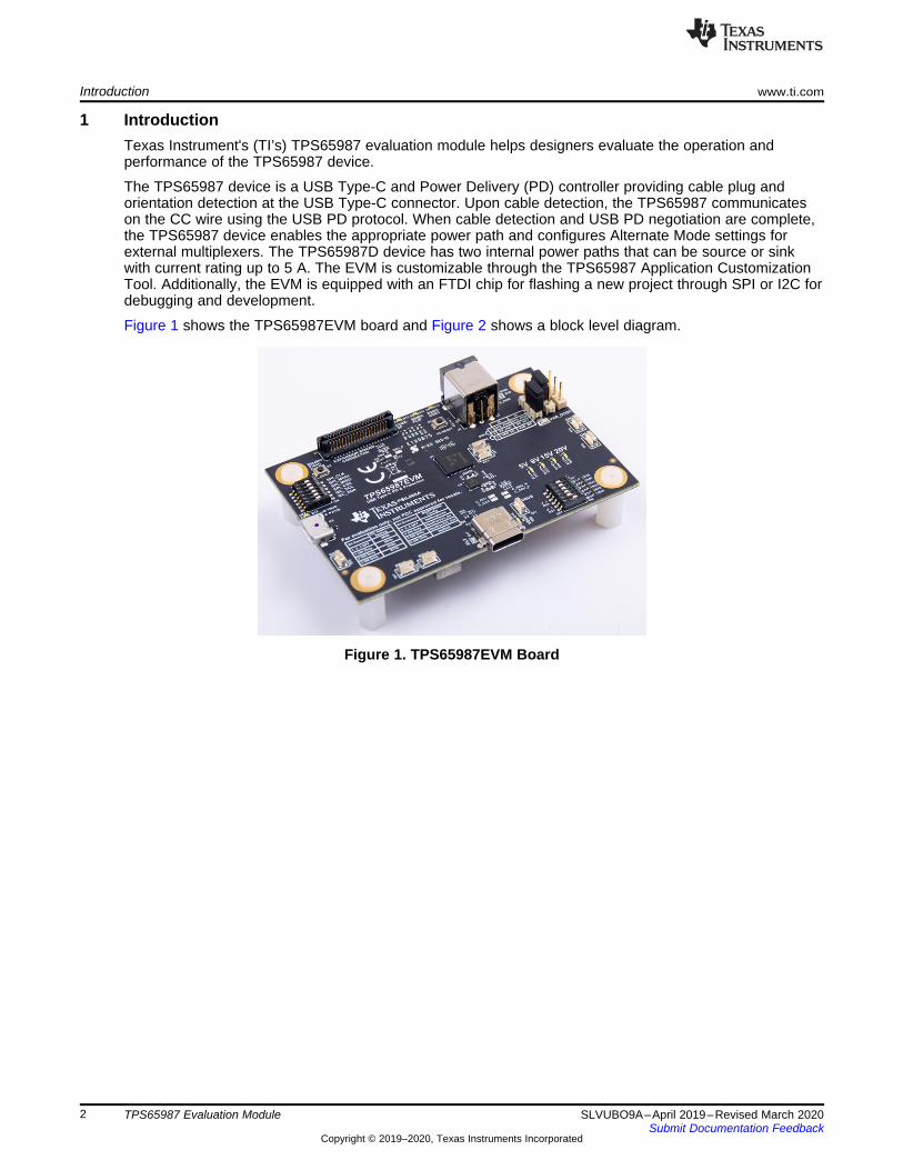
1 IntroductionTexas Instrument's (TI’s) TPS65987 evaluation module helps designers evaluate the operation andperformance of the TPS65987 device.
The TPS65987 device is a USB Type-C and Power Delivery (PD) controller providing cable plug andorientation detection at the USB Type-C connector. Upon cable detection, the TPS65987 communicateson the CC wire using the USB PD protocol. When cable detection and USB PD negotiation are complete,the TPS65987 device enables the appropriate power path and configures Alternate Mode settings forexternal multiplexers. The TPS65987D device has two internal power paths that can be source or sinkwith current rating up to 5 A. The EVM is customizable through the TPS65987 Application CustomizationTool. Additionally, the EVM is equipped with an FTDI chip for flashing a new project through SPI or I2C fordebugging and development.
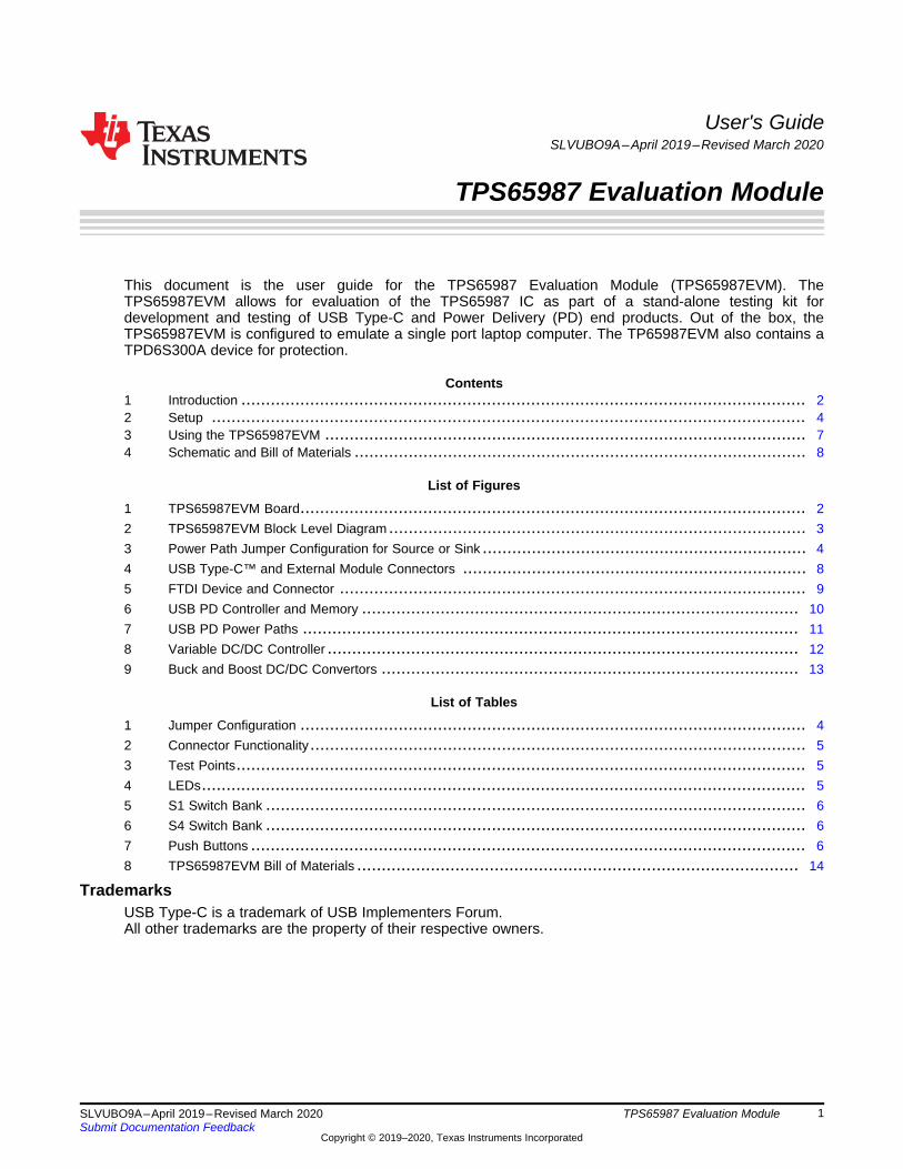
Figure 1 shows the TPS65987EVM board and Figure 2 shows a block level diagram.
Figure 1. TPS65987EVM Board

SBU1/2
Type C
Receptacle
VBUS
CC1/2
SSTX/
RX
USB2.0
TPS65987D
TPD6S300A
C_SBU1/2
C_CC1/2
CC1/2
SBU1/2
CC1/2
Var iable
DC/DC
Buck DC/DC
Boost DC/DC
5V, 9V, 15V,
20V
VIN 3V3
3.3V
VIN 5V
5V
PP_CABLE
SYS PWR
VAR DCSource Path
Sink Path
VIN
VIN 3V3
3.3V
GPIOV_CTL
Expansion connector
PP
EX
T
(GP
IO)
USB2.0
DC Barrel JackJ4
J5
SYS PWR
20V
J9
J1
FTDI
Flash
SPI
Type B (micro)
Receptacle
F-VBUS
USB2.0
J3
J2
SPI
SYS PWR
PFET Control
PPHV1
PPHV2
VIN 5V0
5V
VIN 3V3
VIN 5V0
LDO
AUX/SBU1/2
SSTX/RX
USB D+/D-
J6
I2C
www.ti.com Introduction
3SLVUBO9A–April 2019–Revised March 2020Submit Documentation Feedback
Copyright © 2019–2020, Texas Instruments Incorporated
TPS65987 Evaluation Module
Figure 2. TPS65987EVM Block Level Diagram
1.1 Items Required for OperationThe following is required to operate the EVM:• TPS65987EVM• 20-V barrel jack adapter or dc power supply• Active or e-marked USB Type-C cables• USB Type-A to USB Micro-B cable ( for configuration customization, debugging and updating FW
flash)• TPS65987D USB Type-C and USB PD Controller with Integrated Power Switches data sheet• TPS6598x configuration tool• TPS6598x Application Customization Tool user's guide• How to evaluate and configure TI's USB type-C PD Controllers training videos
SYS_PWR
PP_HV1
VAR_DCDC
1
2
3
SYS_PWR
PP_HV2
VAR_DCDC
TPS65987D
Power Paths
J5 J4
1
2
3
SYS_PWR
PP_HV2
VAR_DCDC
Jumper J6 is not used
J6
Do not populate
sink
source
sink
source
sink
source
Setup www.ti.com
4 SLVUBO9A–April 2019–Revised March 2020Submit Documentation Feedback
Copyright © 2019–2020, Texas Instruments Incorporated
TPS65987 Evaluation Module
2 SetupThis section describes the header and jumper connections on the EVM and getting started using theTPS65987EVM.
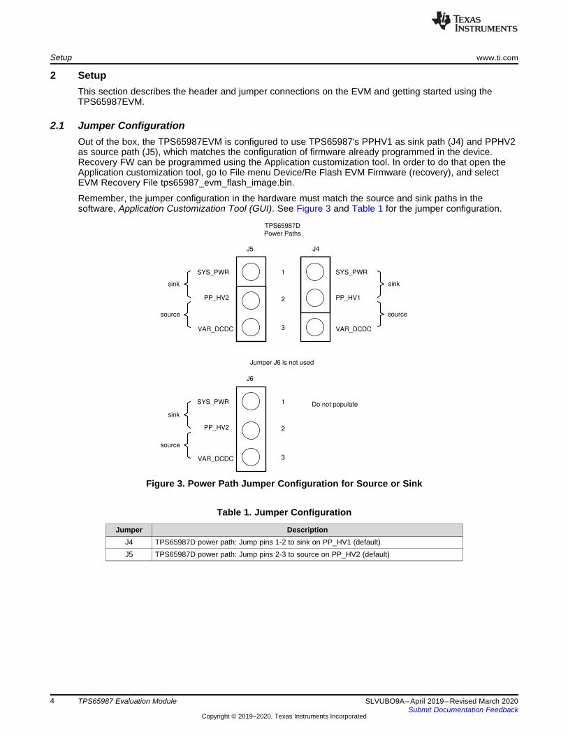
2.1 Jumper ConfigurationOut of the box, the TPS65987EVM is configured to use TPS65987's PPHV1 as sink path (J4) and PPHV2as source path (J5), which matches the configuration of firmware already programmed in the device.Recovery FW can be programmed using the Application customization tool. In order to do that open theApplication customization tool, go to File menu Device/Re Flash EVM Firmware (recovery), and selectEVM Recovery File tps65987_evm_flash_image.bin.
Remember, the jumper configuration in the hardware must match the source and sink paths in thesoftware, Application Customization Tool (GUI). See Figure 3 and Table 1 for the jumper configuration.
Figure 3. Power Path Jumper Configuration for Source or Sink
Table 1. Jumper Configuration
Jumper DescriptionJ4 TPS65987D power path: Jump pins 1-2 to sink on PP_HV1 (default)J5 TPS65987D power path: Jump pins 2-3 to source on PP_HV2 (default)
www.ti.com Setup
5SLVUBO9A–April 2019–Revised March 2020Submit Documentation Feedback
Copyright © 2019–2020, Texas Instruments Incorporated
TPS65987 Evaluation Module
2.2 Connector FunctionalityTable 2 lists the TPS65987EVM connector and functionality.
Table 2. Connector Functionality
Designator DescriptionJ1 USB Type-C connector: TI recommends using an active or e-marked USB Type-c cableJ2 Expansion board connector: Option to connect to external module.J3 Micro-B connector: Connect to a PC to flash a project on the PD controller. You must download the
TPS6598x configuration tool (GUI) to flash a project properly.J9 Barrel jack connector: Use a 19-V to 20-V DC supply. A standard Dell or HP notebook adapter (or similar) will
provide the required power.
2.3 Test PointsTable 3 lists the TPS65987EVM test points.
Table 3. Test Points
Test Point Label DescriptionTP1 VBUS VBUS voltage on the USB Type-C connector. Sourcing and sinking is always in
reference to VBUS (Source to VBUS or sink from VBUS).TP2 CC1 System side CC1. This could be VCONN or CC depending on polarity flip of the USB
Type-C cable.TP3 CC2 System side CC2. This could be VCONN or CC depending on polarity flip of the USB
Type-C cable.TP4, TP5, TP8 GND Ground reference for entire board
TP6 P3V3 Output of 3.3-V DC/DC convertor to power up all ICs on the EVMTP7 P5V0 Output of 5-V DC/DC convertor used for PP_CABLE (VCONN)
2.4 LEDsTable 4 lists the TPS65987EVM LEDs.
Table 4. LEDs
Designator Label DescriptionD12 μB VBUS White LED that shows when the μB port is connected (FTDI for GUI).D13 SSMX: DP White LED that shows when the TPS65987D device has enabled this signal for
external module super-speed MUX (depending on version of EVM the silkscreen mayappear to show this signal swapped with SSMX: USB3)
D14 SSMX: FLIP White LED that shows when the TPS65987D device has enabled this signal forexternal module super-speed MUX
D15 SSMX: USB3 White LED that shows when the TPS65987D device has enabled this signal forexternal module super-speed MUX
D16 VBUS White LED that shows when VBUS has a voltage of 5 V, 9 V, 15 V, or 20 VD19 SYS_PWR Blue LED that shows when the barrel jack is connectedD20 VAR_DCDC Green LED that shows when there is a voltage on the variable DC/DC controller (U9).
When the EVM acts as a source, D20 lights up.D22 PDO_0 White LED that shows when there is a 5-V PD contract (only shown when sourcing)D22 PDO_1 White LED that shows when there is a 9-V PD contract (only shown when sourcing)D24 PDO_2 White LED that shows when there is a 15-V PD contract (only shown when sourcing)D25 PDO_3 White LED that shows when there is a 20-V PD contract (only shown when sourcing)D17 /FLT Red LED that shows when there is an fault occurred TPD6S300A device

Setup www.ti.com
6 SLVUBO9A–April 2019–Revised March 2020Submit Documentation Feedback
Copyright © 2019–2020, Texas Instruments Incorporated
TPS65987 Evaluation Module
2.5 SwitchesTable 5, Table 6, and Table 7 lists the TPS65987EVM switches. For S1, make sure to leave all sixswitches in the ON position (to the right) for flashing a project and debugging. For S4 Switch: EVM out ofth box should have S4->4 (BP_WaitFor3V3_Internal) as on(right). This ensures that PD controller enablesinternal paths in dead battery mode. This switch can be turned off(left) if EVM is used as source only.Note, S4[1, 2, 3] only one switch should be in "ON" position at a time, same way for S4[4, 5, 6].
Table 5. S1 Switch Bank
Switch (S1) Description1: SPI_CLK Connects SPI_CLK node from FTDI to TPS65987D, EEPROM when the switch is in the ON position (to the
right), and disconnects when in the OFF position (to the left)2: SPI_MOSI Connects SPI_MOSI node from FTDI to TPS65987D, EEPROM when the switch is in the ON position (to
the right), and disconnects when in the OFF position (to the left)3: SPI_MISO Connects SPI_MISO node from FTDI to TPS65987D, EEPROM when the switch is in the ON position (to
the right), and disconnects when in the OFF position (to the left)4: SPI_CSZ Connects SPI_CSZ node from FTDI to TPS65987D, EEPROM when the switch is in the ON position (to the
right), and disconnects when in the OFF position (to the left)5: I2C_SCL Connects I2C_SCL node from FTDI to TPS65987D, EEPROM when the switch is in the ON position (to the
right), and disconnects when in the OFF position (to the left)6: I2C_SDA Connects I2C_SDA node from FTDI to TPS65987D, EEPROM when the switch is in the ON position (to the
right), and disconnects when in the OFF position (to the left)
Table 6. S4 Switch Bank
Switch (S4) Description1, 2, 3 OFF I2C address selection: 000b1 ON Only I2C address selection: 001b2 ON Only I2C address selection: 010b3 ON Only I2C address selection: 011b4, 5, 6 OFF Dead battery mode: BP_NoResponse4 ON Only Dead battery mode: BP_WaitFor3V3_Internal5 ON Only Dead battery mode: BP_WaitFor3V3_External6 ON Only Dead battery mode: BP_NoWait
Table 7. Push Buttons
Designator Label DescriptionS2 PD Reset This switch is a push-button that pulls the HRESET pin (44) of the TPS65987D device high
when pressed. Releasing the push-button pulsl HRESET low again, and the TPS65987Ddevice goes through a soft reset, which consists of reloading firmware from RAM. If a validconfiguration is present in RAM, the TPS65987D device will not reload configuration from theexternal flash.
S3 Disable FlashConfig
This push button switch will hold the SPI Miso line to GND. Use this button when booting thedevice. If this button is pressed when the device is booting, the TPS65987D device does notload its configuration from the SPI Flash and instead boots into a default ROM configuration.
www.ti.com Using the TPS65987EVM
7SLVUBO9A–April 2019–Revised March 2020Submit Documentation Feedback
Copyright © 2019–2020, Texas Instruments Incorporated
TPS65987 Evaluation Module
3 Using the TPS65987EVMThis section discusses how to power the EVM, configure the firmware, and how to debug.
3.1 Powering the TPS65987EVMThe main power supply for the EVM is the barrel jack (J9), which accepts 19 V to 20 V via a barrel jackadapter. The EVM can also be powered with an external power supply on SYS_PWR (pin 1 of J4, J5, orJ6). The input voltage can range from 5 V to 20 V, but configure the appropriate power profile for PP_HVin the firmware using the configuration tool. The EVM can also be powered as a sink through a USB Type-C cable from a source adaptor, EVM, or device.
3.2 Firmware ConfigurationsOut of the box, the TPS65987EVM is configured to emulate a single port laptop computer. Thisconfiguration can be used to source or sink power known as (DRP), and this configuration sets DFP_D(Downward Facing Port). If different configurations are required to test your system, use the TPS6598xconfiguration tool(GUI) to create a configuration or load a different configuration template.
3.3 Debugging the EVMThe following checks can help resolve issues when connecting the EVM to another EVM or USB Type-Cdevice and no status LEDs are on:
Make sure that a firmware image is loaded on the TPS65987EVM, using the TPS6598x configurationtool(GUI).
• Make sure the CC lines are toggling for dual-role port functionality.• Make sure the following system supplies:
– P3V3 = 3.3 V– P5V0 = 5 V– Barrel jack / SYS_PWR = 20 V (when plugged in)– VAR_DCDC = 5 V (when barrel jack is plugged in without a USB Type-C attached cable or device)– VBUS = 5 V, 9 V, 15 V, or 20 V (when USB Type-C port is attached to another EVM or device)

GNDA1
TX1+A2
TX1-A3
VBUSA4
CC1A5
D+A6
D-A7
SBU1A8
VBUSA9
RX2-A1 0
RX2+A11
GNDA12 GND B1
B2TX2+
TX2-B3
VBUSB4
CC2B5
D+B6
D-B7
SBU2B8
VBUSB9
RX1-B10
RX1+B11
GND B12
H1 H1
H2 H2
H3 H3H4 H4
H5H5
H6H6
11
22
33
J1
D1
TC_SSTX2_NTC_SSTX2_P
TC_SSTX1_PTC_SSTX1_N
0.01uFC2
0.01uFC3
0.01 uFC4
0.01uFC5
0 C60 C7
1
3
5
2
4
6
7
9 10
8
1211
1413
1615
1817
2019
2221
2423
2625
2827
3029
3231
3433
3635
3837
4039
J2
GNDGND
VBU S
C_SSTX2_N
C_SSTX2_P
GND
C_CC2
C_USB_N
C_USB_P
C_SBU_N
GND
C_SSRX1_P
C_SSRX1_N
GNDGND
C_SSRX2_N
C_SSRX2_P
GND
C_SBU_P
C_U SB_P
C_USB_N
C_CC1
C_SSTX1_P
C_SSTX1_N
GND
GND
VBUS
VBUS
VBUS
0 C90 C8
VBUS
GND
TP1
I2C 1_SCL
I2C1_SDA
C_SSR X2_P
C_SSRX2_N
C_SSTX1_N
C_SSTX1_P
C_SSTX2_P
C_SSTX2_N
C_SSR X1_P
C_SSRX1_N
SBU_P
SBU_N
LDO_3V3
HPD
VAR_DCDC
P5V0
P3V3
C_USB_P
C_U SB_N
GPIO_5/I2C3_SCL
GPIO_6/I2C3_SDA
I2C_SCL_SAM
USB Type-C Connector
Expansion Connector
I2C_SDA_SAM
4.7uFC1
3.48R1
SSM X_DP
SSM X_FLIP
SSMX_USB3
I2C1_IRQZ
GPIO_7/I2C3_IRQZI2C_IRQ_SAM
C_SBU_N
C_SBU_P DP_SBU_P
DP_SBU_N
D3D2 D5D4 D6 D7 D8 D9 D10 D11
DP_SBU_N
DP_SBU_P SBU_P
SBU_N
R2R3
DD
NN
PP
00
R4R5
DD
NN
PP
00
0R60
DN P0
R7R8
0DN P
0R9R10R11 0
DNP
CC1
CC2
C_ CC1
C_CC20R93
DNP
R96 0DNP
SBU_P
SBU_N
R90 0
R91 0
1C_SBU1
2C_SBU2
3VBIAS
4C_CC1
5C_CC2
6RPD_G2
7RPD_G1
GND8
FLT 9VPWR10
CC211
CC112
GND13
SBU214
SBU115
NC16
NC17
GND18
D219
D1 20
PAD21
U2
TPD6S300ARUKR
GND
GND
C_CC1
C_CC2
R76 0
R77 0
0.1uF
C48
GND
3
1
2
Q9
P3V3
GND
Red
12
D17
10.0kR83
CC1
CC2
LDO_3V3
1uF
C43
GND
100kR79
LDO_3V3
/FLT
/FLT
C_USB_P
C_USB_N
Protection Circuit
0C_SBU_P
R94
0C_SBU_N
R97
0/FLT_TPD
R171
Schematic and Bill of Materials www.ti.com
8 SLVUBO9A–April 2019–Revised March 2020Submit Documentation Feedback
Copyright © 2019–2020, Texas Instruments Incorporated
TPS65987 Evaluation Module
4 Schematic and Bill of Materials
4.1 SchematicFigure 4 to Figure 9 illustrate the TPS65987EVM schematics.
Figure 4. USB Type-C™ and External Module Connectors

50VREGIN
49VREGOUT
DM7
REF6
14 RESET#
EECS63
EECLK62
61EEDATA
2OSCI
3OSCO
16ADBUS0
4VPHY
9VPLL
VCORE12
VCCIO20
AGND10
1 GND
36SUSPEND#
60PWREN#
13 TEST
DP8
17ADBUS118ADBUS219ADBUS321ADBUS422ADBUS523
ADBUS624
ADBUS7
26BDBUS0
27BDBUS1
29BDBUS3
28BDBUS2
30BDBUS4
32BDBUS5
33BDBUS634BDBUS7
38CDBU S039CDBU S140
CDBU S241
CDBU S343
CDBU S444
CDBU S545
CDBU S646
CDBU S7
48DDBU S0
52DDBU S1
53DDBU S254DDBU S355DDBU S457DDBU S558DDBU S659
DDBU S7
5 GND
GND11
GND15
GND25
GND47
GND51
37 VCORE64 VCORE
VCCIO31
VCCIO42
VCCIO5 6
GND35
U4
FT4232HL
12
Y1
27pF
C24
27pF
C23
2VSS
DI3
6VCC
CS5
4CLK
DO1
U7
93LC56BT-I/OT
GND
GND
GND
GND
GND
R25DN
NPP
00R26
D
GND
D+1
D-2
3GND
U3
TPD2E009DRTRGND
F_USB_D_N
L1 26 ohm
0.01uFC25
RESETN
White
12
D12
GND
F_SPI_CLK
F_SPI_MOSI
F_SPI_MISO
F_SPI_CSZ
F_I2C2_SCL
F_I2C2_SDA
VREGOUT
GND
GND
VREGOUT
EEC LK
EECS
EEDATA
GND
GND
F_USB_D_P
GND
GND
F_USB_D_P
F_ USB_D_N
F_ USB_D_P F_USB_D_N
EECLK
EECS
EEDATA
EEDATA
F_SPI_CLK
F_SPI_MOSI
F_SPI_MISO
F_SPI_CSZ
SPI_MOSI
SPI_MISO
SPI_CSZ
SPI_CLK
SWD_DATA
SWD_CLK
1
2
Make sure to keep Y1 traces the same length
3
4
5
6
1
9
8
7
0
11
12
S1
F_I2C2 _SCL
F_I 2C2_SDA
I2C2_SCL
I2C2_SDA
10.0kR23
1.00k
R21
4.70kR20
GND
RESETN
F_VBUS
FTDI Chip
Micro-B Connector
FTDI Switches and Memory
10.0kR24
10.0kR27
GND
ULINK2 Debugger
10.0kR22
0.1uF
C10
0.1uFC15
0.1uFC12
0.1uFC14
0.1uFC16
0.1uFC19
0.1uFC18
0.1uFC20
0.1u FC21
0
R18
0DNP
R19
0
DNP
R17
12k
R16
10.0kR12
10.0kR13
10.0kR14
0.1uFC17
2.20k
R15
4.7uF
C11
4.7uF
C13
4.7uFC22
GND
F_VBUS
GND
GND GND
F_SYS_3V3
F_SYS_3V3
F_SYS_3V3
F_SYS_3V3
F_SYS_3V3
1
F_SYS_3V3
EN2
3 IN
IN4
5OUT6OUT
NC 7
8PG
GND
U13 TPS76833QD
0.1uF
C44249k
0
R164
R170 10µF
C45 10uFC46
1VBUS
D-2
D+3
4ID
5GND
67
8
91
0
J3
LDO_3V3
www.ti.com Schematic and Bill of Materials
9SLVUBO9A–April 2019–Revised March 2020Submit Documentation Feedback
Copyright © 2019–2020, Texas Instruments Incorporated
TPS65987 Evaluation Module
Figure 5. FTDI Device and Connector

21
S2
TP2
TP3
SPI_MISO Pull Downto disable flash config
Variable DC/DC ControlSS Mux Control
SSMX_DP --> GPIO_0SSMX_FLIP --> GPIO_1SSMX_USB3 --> GPIO_2
HPD --> GPIO3
I2C Addr ess SettingSwitch 1-3 Off --> 000b (0)Switch 1 On only --> 001b (0.34)Switch 2 On only --> 010b (0.50)Switch 3 On only --> 011b (0.90)
Truth Table
5V
1
Output Voltage
2 3 4 5 6
1 9 8 7
0
11
12
S4
GN DGND
21
S3
GND
BUSPOWERZ Configur ationSwitch 4-6 Off --> BP_NoResponse (0)Switch 4 On only --> BP_WaitFor3V3_Internal (0.24)Switch 5 On only --> BP_WaitFor3V3_External (0.43)Switch 6 On only --> BP_NoWait (0.90)
GND
HPD
SSMX_DP
SSMX_FLIP
SSMX_USB3
GPIO_5/I2C3_SCL
GPIO_6/I2C3_SDA
GND
GNDGND
SSMX_USB3SSMX_FLIPSSMX_DP
P3V3
SPI_MISO
SPI_CSZ
SPI_CLK
SPI_MOSI
SPI_MISO
PD O_1
PDO_0
ADCIN2 ADCIN1
LDO_3V3
P3V3
LDO_3V3
HRESET
SWD_CLK
I2C1_SCL
I2C1_SDA
I2C2_SCL
I2C2_IRQZ
I2C2_SDA
I2C1_IRQZ220pFC26
220pFC27
GND GND
CC1
CC2
C_USB_P
C_USB_N
PP_EXT2_EN
SWD_DATA
PDO_3
/PGOOD
GPIO_7/I2C3_IRQZ
ADCIN2
ADCIN1
GND
LDO_3V3
USB PD Controller
EEPROM
SS Mux Control LED's
ADCIN1:2 Resistor Divider Setting
PDO_2
0PDO_3
00
00
0
0
001
PDO_2 PDO_1
11 9V
15V20V
10.0kR30
10.0kR34
3.83kR28
3.83kR29
3.83kR36
10.0kR44
10.0kR41
100kR40
191kR39
100k
R50
100k
0
R51
0
R49
R37
100kR38
CS1
2 SO/SIO1
W P3
GND 4
5 SI/SIO0
6 SCLK
7HOLD
8VCC
U5
MX25L8006EM1I-12G
LDO_3V3
0.1uFC29
GND
GND
SPI_CSZ
SPI_CLK
SPI_M OSI
SPI_MISO
3.3kR46
3.3kR47
3.3kR48
3.3kR45
SPI_C SZ
SPI_MISO
10.0kR32
10.0kR33
White
12
D14White
12
D13White
12
D15
130kR43
316kR42
DNR1300P
GND
/FLT_TPD
10.0kR31
3.83kR35
6ADCIN1
10ADCIN2
C1_CC124
26C1_CC2
53C_USB_N (GPIO19)
50
GND
C1_USB_P (GPIO18)
45
GND 47
55GPIO21
54GPIO20
16GPIO0
GPIO117
40 GPIO1241 GPIO1342
GPIO14 (PWM)43
GPIO15 (PWM)48
GPIO16 (PEXT1)49
GPIO17 (PEXT2)
18GPIO2
21I2C3_SCL (GPIO5)
22I2C3_SDA (GPIO6)
30HPD (GPIO3)
GPIO431
44HRESET
29I2C1_IRQ
27I2C1_SCL
28I2C1_SD A
34I2C2 _IRQ
32I2C2_SCL33I2C2_SD A
38 SPI_CLK (GPIO10)
36SPI_MISO (GPIO8)
37 SPI_MOSI (GPIO9)
39 SPI_SS (GPIO11)
23I2C3_IRQ (GPIO7)
U1A
3
1
TPS65987DDHRSHR
2
Q1
3
1
SI1012R-T1-GE3
2
Q2
3
1
SI1012R-T1-GE3
2
Q3
0 SI1012R-T1-GE3
0R172R173
PD_U SB_PPD_U SB_N
0.01uF
C28
Schematic and Bill of Materials www.ti.com
10 SLVUBO9A–April 2019–Revised March 2020Submit Documentation Feedback
Copyright © 2019–2020, Texas Instruments Incorporated
TPS65987 Evaluation Module
Figure 6. USB PD Controller and Memory
GND
GND
GND
3
1
2
Q5
22uFC31
10uFC42
3
1
2
4
5
V+
V-
U6
3
1
2
Q6
GND
GND
10uFC40
GND
10uFC41
22uFC30
GND
DRAIN1
DRAIN2
PP_EXT1
GND
LDO_3V3
LDO_1V8
P5V0
10uFC38
10uFC37
GND GND
P3V3
PP_HV1
GND
VBUS
VBUS
GN D
GND
PP_EXT2_EN
LDO_3V3
External Power Path (PD Controller )
USB PD Power Path
PP_CAB_87
22uF
C39
GND
PP_HV2White
12
D16
GND
0.1uF50V
C35
100kPR62
DN
10.0kR66
10.0kR60
10.0k
R57
10.0kR55
1.00k
R61
1P0.0k
R54DN
10.0kPR56
DN
576k
R65
0.1uFDNPC34
0.1uFC33
1uFC36
2
1
7,8
Q4A
4
3
5,6
Q4B
60.4kR59
60.4kR58
10.0k
R63
10.0k
R64
0.1uFC32
R67 0
R68DN
0P
GND
DNP0R131
P3V3
35LDO_1V8
9LDO_ 3V3
15 DRAIN1
25PP1_CABLE
GND46
12PP_HV1
11PP_ HV1
1PP_HV22PP_HV2
13VBUS1
14VBUS1
3VBUS2
4VBUS2
5VIN_3V3
56DRAIN2
DRAIN257
7 DRAIN2
8DRAIN1
19 DRAIN158 DRAIN1
DRAIN252
GND51
GND20
GND59
U1B
1
3
J4
SYS_PW R
VAR_DCDC
PP_HV1
1
2
3
J5
SYS_PWR
PP Jumpers
SYS_PWR =>Sink from VBUSVAR_DCDC=>Source to VBUS
VAR_DCDC
PP_HV2
SYS_PWR
VAR_DCDC
PP_EXT1
1
2
3
J6
TPS65987DDHRSHR
2
www.ti.com Schematic and Bill of Materials
11SLVUBO9A–April 2019–Revised March 2020Submit Documentation Feedback
Copyright © 2019–2020, Texas Instruments Incorporated
TPS65987 Evaluation Module
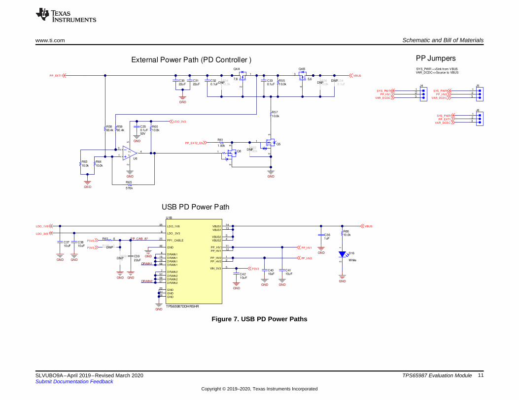
Figure 7. USB PD Power Paths
22uFC52
22uFC53
GND
GND
270
R103
0.1uFC54
Output capacitors must be rated toat least 25V and have ESR in 100s of mOhms
GND
GND
GND
22uF25V
C6022uF25V
C6122uF25V
C6222uF25V
C6322uF25V
C6422uF25V
C6522uF25V
C6622uF25V
C6722uF25V
C6822uF25V
C6922uF25V
C7022uF25V
C7122uF25V
C72
SYS_PWR
EN _VAR
GND
GND
10kR104
PDO_ 2PDO_1
P3V3
22uF25V
C59
SYS_PW R
30kR100
GND
9.53kR107
0.1uFC56
Green
21
D20
8.87kR111
1
23
Q11 1
23
Q12 1
23
Q13
1
23
Q14
3.65kR112
47uFC50
47uFC51
VA R_DCDC
EN_VAR
PDO_1 PD O_2 PDO_3
GND
PDO_2 PDO_10 0
10
010 0
5V
9V15V20V
Output Voltage Feedback (R1)30k
30k
Feedback (R2)
30k30k
9.53k
4.59k2.64k1.79k
5.14V
9.33V15.3222.03
PDO_3 Output Voltage00
01
1
23
Q16 1
23
Q17PDO_0
1
23
Q15
Variable DC/DC Convertor: 5V, 9V, 15V, 20V
Var. DC/DC Control LED'sFast Role Swap Caps
Change PDO's
GND
PDO_31
23
Q18
2.20kR113
IN4
IN5
1G
ND
2G
ND
IN6
3G
ND
7P
AD
U8
GND
10.0kR114
10.0kR115
10.0kR116
10.0kR117
100kR102
11.0k
1
R106
000pF
C55
1000pFC581
3
2
D21
DNP
GND
SYS_PWR
1
3
2
D18
10uH
L2
4
7,81,2,3
5,6,
Q10
47.5kR99
100pFC57
SW_Node_VARDC
100k
FB node on VAR_DC
R109100kR110
100kR108
10.0kR105
100kR101
DNP0R98
GND
White
12
D23
White
12
D24
White
12
D22
White
12
D255V 9V 15V 20V
TP5
TP4
1
Blue
2
D19
1SENSE
4GND
2POWER
3POWER
5GND
6 SHIELD7 SHIELD8 SHIELD9
J9
SHIELD
JPD1135-509-7F1
ISENSE
2GND
3EN
FB4
5ADJ
6PGND
7PGATE
8 VIN
U9
LM3489QMM/NOPB
TP8
GND
Schematic and Bill of Materials www.ti.com
12 SLVUBO9A–April 2019–Revised March 2020Submit Documentation Feedback
Copyright © 2019–2020, Texas Instruments Incorporated
TPS65987 Evaluation Module
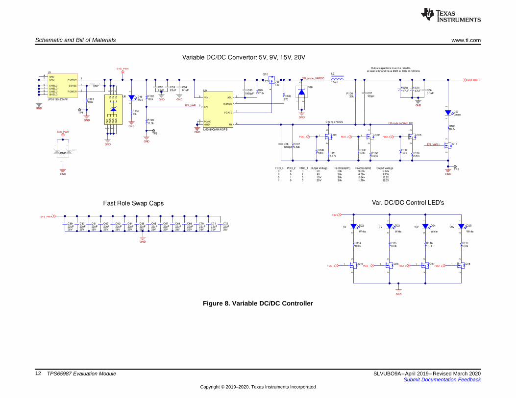
Figure 8. Variable DC/DC Controller

SW
2PGND
SW Node Boost1
IN3
4 EN5GND
6 ILIM
7ENUSB
8FAULT USB
9
AUX10
EP 11
U12
TPS2500DRCR
0.1uF50V
C74
0.1uFC76
GND
GND
GND
10uH
L3
GND
0.1uFC85
GND
GND
ILim setMax 1100mATyp 900mAMin 700mA
2.2uH
L4
0.1uFC79
GND
22uFC75
1 VIN
6VSENSE
8EN
PGOOD10
3GND
7COMP
PH2
9BOOT
PAD11
GND4
5GND
U10
TPS54334DRCR
300pFC82
2.61kR124
6800pFC83
GND
PG
D_
3V
3
GND
47uFC88
100kR122
32.4kR127
150kR120
66.5kR126
32.4kR129
TP6
TP7
47uF
C77
47uF
C78
47uF
C86
47uF
C840.1uFC87
47uF
C49
SYS_PWR
P5V0
GND
GND
P3V3
P3V3
P3V3
220pFC81
Buck Convertor: SYS_PW R => 3.3V
V3V3_Sense
&
Boost Convertor: 3.3V => 5V
3
4
1
62
V+
V-
5
U11
560k
R125
39k
R123
GND
GND
100kR118
15.0kR121
GND
22pFC80
GND
0
R119
0.1uFC73
SYS_PWR
P3V3
/PGOOD
Barrel Jack Detection
100k
R128
SW Node Buck
PGD_3V3
www.ti.com Schematic and Bill of Materials
13SLVUBO9A–April 2019–Revised March 2020Submit Documentation Feedback
Copyright © 2019–2020, Texas Instruments Incorporated
TPS65987 Evaluation Module
Figure 9. Buck and Boost DC/DC Convertors
Schematic and Bill of Materials www.ti.com
14 SLVUBO9A–April 2019–Revised March 2020Submit Documentation Feedback
Copyright © 2019–2020, Texas Instruments Incorporated
TPS65987 Evaluation Module
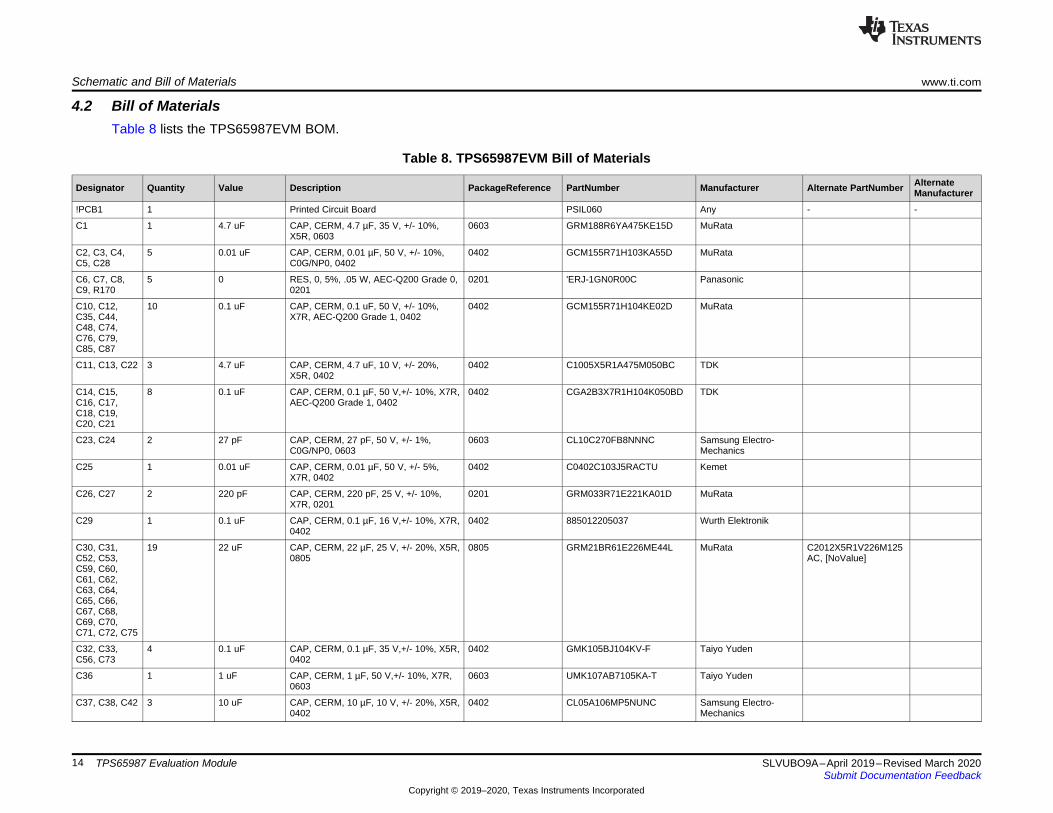
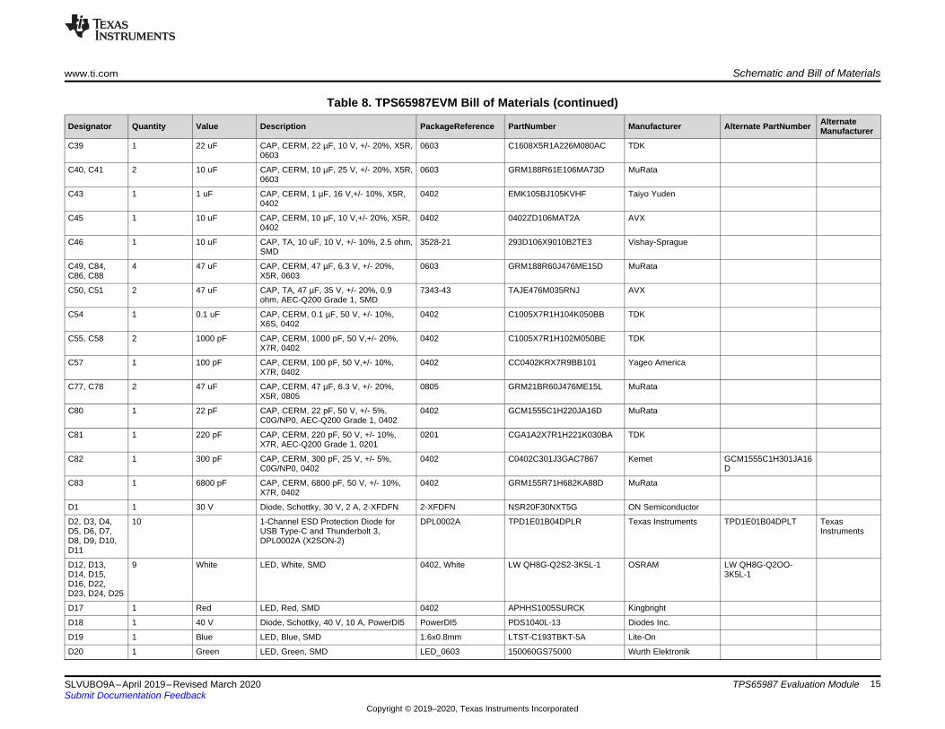
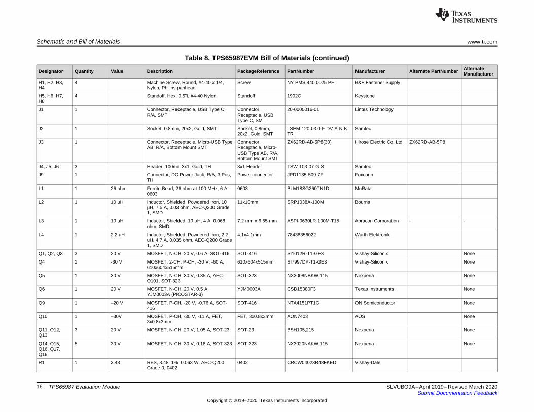
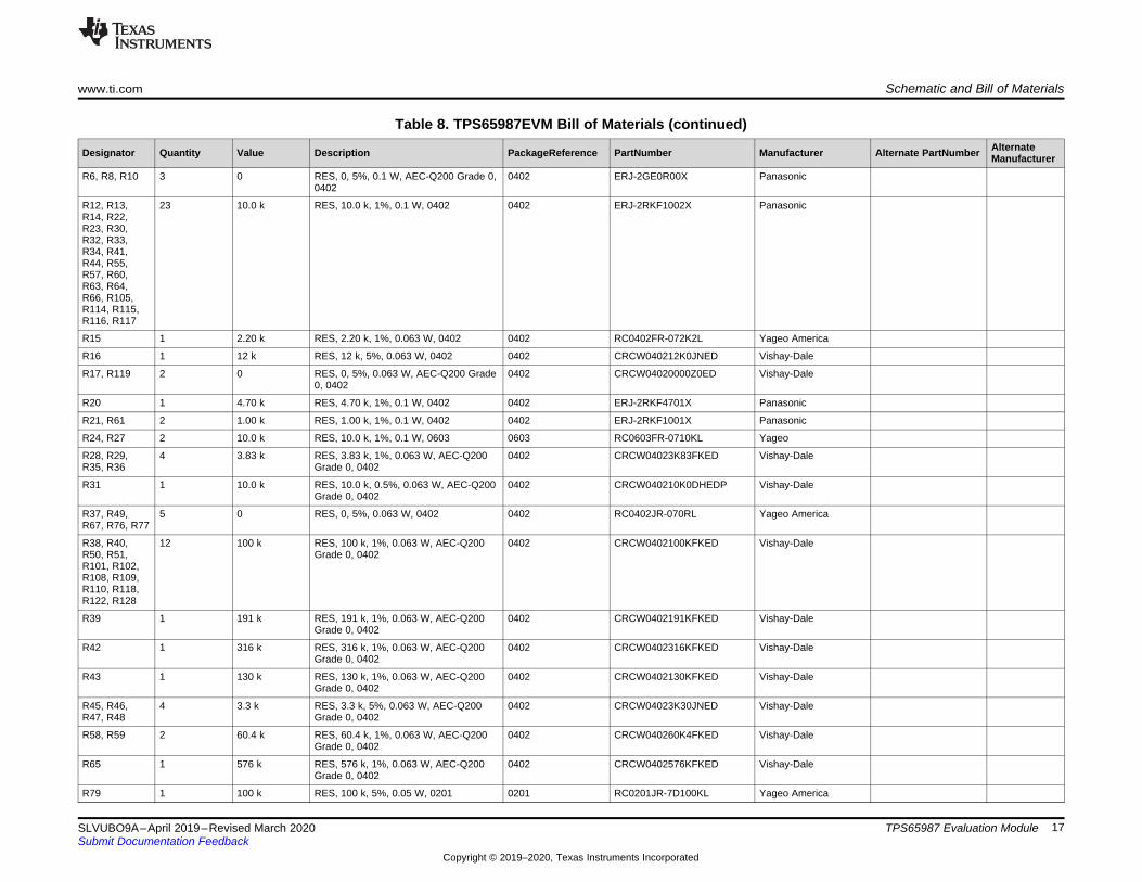
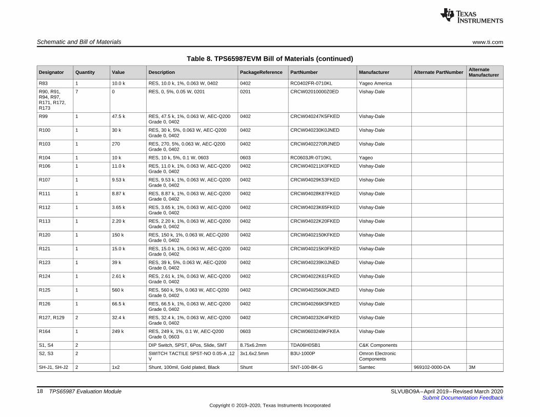
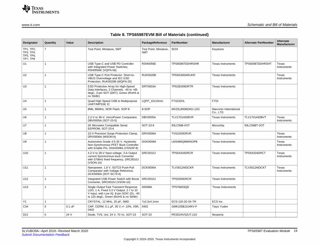
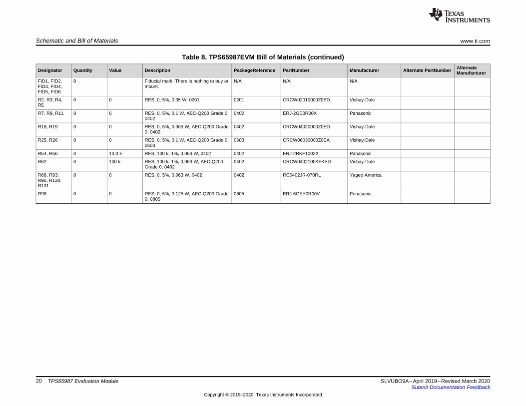
4.2 Bill of MaterialsTable 8 lists the TPS65987EVM BOM.
Table 8. TPS65987EVM Bill of Materials
Designator Quantity Value Description PackageReference PartNumber Manufacturer Alternate PartNumber AlternateManufacturer
!PCB1 1 Printed Circuit Board PSIL060 Any - -
C1 1 4.7 uF CAP, CERM, 4.7 µF, 35 V, +/- 10%,X5R, 0603
0603 GRM188R6YA475KE15D MuRata
C2, C3, C4,C5, C28
5 0.01 uF CAP, CERM, 0.01 µF, 50 V, +/- 10%,C0G/NP0, 0402
0402 GCM155R71H103KA55D MuRata
C6, C7, C8,C9, R170
5 0 RES, 0, 5%, .05 W, AEC-Q200 Grade 0,0201
0201 'ERJ-1GN0R00C Panasonic
C10, C12,C35, C44,C48, C74,C76, C79,C85, C87
10 0.1 uF CAP, CERM, 0.1 uF, 50 V, +/- 10%,X7R, AEC-Q200 Grade 1, 0402
0402 GCM155R71H104KE02D MuRata
C11, C13, C22 3 4.7 uF CAP, CERM, 4.7 uF, 10 V, +/- 20%,X5R, 0402
0402 C1005X5R1A475M050BC TDK
C14, C15,C16, C17,C18, C19,C20, C21
8 0.1 uF CAP, CERM, 0.1 µF, 50 V,+/- 10%, X7R,AEC-Q200 Grade 1, 0402
0402 CGA2B3X7R1H104K050BD TDK
C23, C24 2 27 pF CAP, CERM, 27 pF, 50 V, +/- 1%,C0G/NP0, 0603
0603 CL10C270FB8NNNC Samsung Electro-Mechanics
C25 1 0.01 uF CAP, CERM, 0.01 µF, 50 V, +/- 5%,X7R, 0402
0402 C0402C103J5RACTU Kemet
C26, C27 2 220 pF CAP, CERM, 220 pF, 25 V, +/- 10%,X7R, 0201
0201 GRM033R71E221KA01D MuRata
C29 1 0.1 uF CAP, CERM, 0.1 µF, 16 V,+/- 10%, X7R,0402
0402 885012205037 Wurth Elektronik
C30, C31,C52, C53,C59, C60,C61, C62,C63, C64,C65, C66,C67, C68,C69, C70,C71, C72, C75
19 22 uF CAP, CERM, 22 µF, 25 V, +/- 20%, X5R,0805
0805 GRM21BR61E226ME44L MuRata C2012X5R1V226M125AC, [NoValue]
C32, C33,C56, C73
4 0.1 uF CAP, CERM, 0.1 µF, 35 V,+/- 10%, X5R,0402
0402 GMK105BJ104KV-F Taiyo Yuden
C36 1 1 uF CAP, CERM, 1 µF, 50 V,+/- 10%, X7R,0603
0603 UMK107AB7105KA-T Taiyo Yuden
C37, C38, C42 3 10 uF CAP, CERM, 10 µF, 10 V, +/- 20%, X5R,0402
0402 CL05A106MP5NUNC Samsung Electro-Mechanics
www.ti.com Schematic and Bill of Materials
15SLVUBO9A–April 2019–Revised March 2020Submit Documentation Feedback
Copyright © 2019–2020, Texas Instruments Incorporated
TPS65987 Evaluation Module
Table 8. TPS65987EVM Bill of Materials (continued)
Designator Quantity Value Description PackageReference PartNumber Manufacturer Alternate PartNumber AlternateManufacturer
C39 1 22 uF CAP, CERM, 22 µF, 10 V, +/- 20%, X5R,0603
0603 C1608X5R1A226M080AC TDK
C40, C41 2 10 uF CAP, CERM, 10 µF, 25 V, +/- 20%, X5R,0603
0603 GRM188R61E106MA73D MuRata
C43 1 1 uF CAP, CERM, 1 µF, 16 V,+/- 10%, X5R,0402
0402 EMK105BJ105KVHF Taiyo Yuden
C45 1 10 uF CAP, CERM, 10 µF, 10 V,+/- 20%, X5R,0402
0402 0402ZD106MAT2A AVX
C46 1 10 uF CAP, TA, 10 uF, 10 V, +/- 10%, 2.5 ohm,SMD
3528-21 293D106X9010B2TE3 Vishay-Sprague
C49, C84,C86, C88
4 47 uF CAP, CERM, 47 µF, 6.3 V, +/- 20%,X5R, 0603
0603 GRM188R60J476ME15D MuRata
C50, C51 2 47 uF CAP, TA, 47 µF, 35 V, +/- 20%, 0.9ohm, AEC-Q200 Grade 1, SMD
7343-43 TAJE476M035RNJ AVX
C54 1 0.1 uF CAP, CERM, 0.1 µF, 50 V, +/- 10%,X6S, 0402
0402 C1005X7R1H104K050BB TDK
C55, C58 2 1000 pF CAP, CERM, 1000 pF, 50 V,+/- 20%,X7R, 0402
0402 C1005X7R1H102M050BE TDK
C57 1 100 pF CAP, CERM, 100 pF, 50 V,+/- 10%,X7R, 0402
0402 CC0402KRX7R9BB101 Yageo America
C77, C78 2 47 uF CAP, CERM, 47 µF, 6.3 V, +/- 20%,X5R, 0805
0805 GRM21BR60J476ME15L MuRata
C80 1 22 pF CAP, CERM, 22 pF, 50 V, +/- 5%,C0G/NP0, AEC-Q200 Grade 1, 0402
0402 GCM1555C1H220JA16D MuRata
C81 1 220 pF CAP, CERM, 220 pF, 50 V, +/- 10%,X7R, AEC-Q200 Grade 1, 0201
0201 CGA1A2X7R1H221K030BA TDK
C82 1 300 pF CAP, CERM, 300 pF, 25 V, +/- 5%,C0G/NP0, 0402
0402 C0402C301J3GAC7867 Kemet GCM1555C1H301JA16D
C83 1 6800 pF CAP, CERM, 6800 pF, 50 V, +/- 10%,X7R, 0402
0402 GRM155R71H682KA88D MuRata
D1 1 30 V Diode, Schottky, 30 V, 2 A, 2-XFDFN 2-XFDFN NSR20F30NXT5G ON Semiconductor
D2, D3, D4,D5, D6, D7,D8, D9, D10,D11
10 1-Channel ESD Protection Diode forUSB Type-C and Thunderbolt 3,DPL0002A (X2SON-2)
DPL0002A TPD1E01B04DPLR Texas Instruments TPD1E01B04DPLT TexasInstruments
D12, D13,D14, D15,D16, D22,D23, D24, D25
9 White LED, White, SMD 0402, White LW QH8G-Q2S2-3K5L-1 OSRAM LW QH8G-Q2OO-3K5L-1
D17 1 Red LED, Red, SMD 0402 APHHS1005SURCK Kingbright
D18 1 40 V Diode, Schottky, 40 V, 10 A, PowerDI5 PowerDI5 PDS1040L-13 Diodes Inc.
D19 1 Blue LED, Blue, SMD 1.6x0.8mm LTST-C193TBKT-5A Lite-On
D20 1 Green LED, Green, SMD LED_0603 150060GS75000 Wurth Elektronik
Schematic and Bill of Materials www.ti.com
16 SLVUBO9A–April 2019–Revised March 2020Submit Documentation Feedback
Copyright © 2019–2020, Texas Instruments Incorporated
TPS65987 Evaluation Module
Table 8. TPS65987EVM Bill of Materials (continued)
Designator Quantity Value Description PackageReference PartNumber Manufacturer Alternate PartNumber AlternateManufacturer
H1, H2, H3,H4
4 Machine Screw, Round, #4-40 x 1/4,Nylon, Philips panhead
Screw NY PMS 440 0025 PH B&F Fastener Supply
H5, H6, H7,H8
4 Standoff, Hex, 0.5"L #4-40 Nylon Standoff 1902C Keystone
J1 1 Connector, Receptacle, USB Type C,R/A, SMT
Connector,Receptacle, USBType C, SMT
20-0000016-01 Lintes Technology
J2 1 Socket, 0.8mm, 20x2, Gold, SMT Socket, 0.8mm,20x2, Gold, SMT
LSEM-120-03.0-F-DV-A-N-K-TR
Samtec
J3 1 Connector, Receptacle, Micro-USB TypeAB, R/A, Bottom Mount SMT
Connector,Receptacle, Micro-USB Type AB, R/A,Bottom Mount SMT
ZX62RD-AB-5P8(30) Hirose Electric Co. Ltd. ZX62RD-AB-5P8
J4, J5, J6 3 Header, 100mil, 3x1, Gold, TH 3x1 Header TSW-103-07-G-S Samtec
J9 1 Connector, DC Power Jack, R/A, 3 Pos,TH
Power connector JPD1135-509-7F Foxconn
L1 1 26 ohm Ferrite Bead, 26 ohm at 100 MHz, 6 A,0603
0603 BLM18SG260TN1D MuRata
L2 1 10 uH Inductor, Shielded, Powdered Iron, 10µH, 7.5 A, 0.03 ohm, AEC-Q200 Grade1, SMD
11x10mm SRP1038A-100M Bourns
L3 1 10 uH Inductor, Shielded, 10 µH, 4 A, 0.068ohm, SMD
7.2 mm x 6.65 mm ASPI-0630LR-100M-T15 Abracon Corporation - -
L4 1 2.2 uH Inductor, Shielded, Powdered Iron, 2.2uH, 4.7 A, 0.035 ohm, AEC-Q200 Grade1, SMD
4.1x4.1mm 78438356022 Wurth Elektronik
Q1, Q2, Q3 3 20 V MOSFET, N-CH, 20 V, 0.6 A, SOT-416 SOT-416 SI1012R-T1-GE3 Vishay-Siliconix None
Q4 1 -30 V MOSFET, 2-CH, P-CH, -30 V, -60 A,610x604x515mm
610x604x515mm SI7997DP-T1-GE3 Vishay-Siliconix None
Q5 1 30 V MOSFET, N-CH, 30 V, 0.35 A, AEC-Q101, SOT-323
SOT-323 NX3008NBKW,115 Nexperia None
Q6 1 20 V MOSFET, N-CH, 20 V, 0.5 A,YJM0003A (PICOSTAR-3)
YJM0003A CSD15380F3 Texas Instruments None
Q9 1 –20 V MOSFET, P-CH, -20 V, -0.76 A, SOT-416
SOT-416 NTA4151PT1G ON Semiconductor None
Q10 1 –30V MOSFET, P-CH, -30 V, -11 A, FET,3x0.8x3mm
FET, 3x0.8x3mm AON7403 AOS None
Q11, Q12,Q13
3 20 V MOSFET, N-CH, 20 V, 1.05 A, SOT-23 SOT-23 BSH105,215 Nexperia None
Q14, Q15,Q16, Q17,Q18
5 30 V MOSFET, N-CH, 30 V, 0.18 A, SOT-323 SOT-323 NX3020NAKW,115 Nexperia None
R1 1 3.48 RES, 3.48, 1%, 0.063 W, AEC-Q200Grade 0, 0402
0402 CRCW04023R48FKED Vishay-Dale
www.ti.com Schematic and Bill of Materials
17SLVUBO9A–April 2019–Revised March 2020Submit Documentation Feedback
Copyright © 2019–2020, Texas Instruments Incorporated
TPS65987 Evaluation Module
Table 8. TPS65987EVM Bill of Materials (continued)
Designator Quantity Value Description PackageReference PartNumber Manufacturer Alternate PartNumber AlternateManufacturer
R6, R8, R10 3 0 RES, 0, 5%, 0.1 W, AEC-Q200 Grade 0,0402
0402 ERJ-2GE0R00X Panasonic
R12, R13,R14, R22,R23, R30,R32, R33,R34, R41,R44, R55,R57, R60,R63, R64,R66, R105,R114, R115,R116, R117
23 10.0 k RES, 10.0 k, 1%, 0.1 W, 0402 0402 ERJ-2RKF1002X Panasonic
R15 1 2.20 k RES, 2.20 k, 1%, 0.063 W, 0402 0402 RC0402FR-072K2L Yageo America
R16 1 12 k RES, 12 k, 5%, 0.063 W, 0402 0402 CRCW040212K0JNED Vishay-Dale
R17, R119 2 0 RES, 0, 5%, 0.063 W, AEC-Q200 Grade0, 0402
0402 CRCW04020000Z0ED Vishay-Dale
R20 1 4.70 k RES, 4.70 k, 1%, 0.1 W, 0402 0402 ERJ-2RKF4701X Panasonic
R21, R61 2 1.00 k RES, 1.00 k, 1%, 0.1 W, 0402 0402 ERJ-2RKF1001X Panasonic
R24, R27 2 10.0 k RES, 10.0 k, 1%, 0.1 W, 0603 0603 RC0603FR-0710KL Yageo
R28, R29,R35, R36
4 3.83 k RES, 3.83 k, 1%, 0.063 W, AEC-Q200Grade 0, 0402
0402 CRCW04023K83FKED Vishay-Dale
R31 1 10.0 k RES, 10.0 k, 0.5%, 0.063 W, AEC-Q200Grade 0, 0402
0402 CRCW040210K0DHEDP Vishay-Dale
R37, R49,R67, R76, R77
5 0 RES, 0, 5%, 0.063 W, 0402 0402 RC0402JR-070RL Yageo America
R38, R40,R50, R51,R101, R102,R108, R109,R110, R118,R122, R128
12 100 k RES, 100 k, 1%, 0.063 W, AEC-Q200Grade 0, 0402
0402 CRCW0402100KFKED Vishay-Dale
R39 1 191 k RES, 191 k, 1%, 0.063 W, AEC-Q200Grade 0, 0402
0402 CRCW0402191KFKED Vishay-Dale
R42 1 316 k RES, 316 k, 1%, 0.063 W, AEC-Q200Grade 0, 0402
0402 CRCW0402316KFKED Vishay-Dale
R43 1 130 k RES, 130 k, 1%, 0.063 W, AEC-Q200Grade 0, 0402
0402 CRCW0402130KFKED Vishay-Dale
R45, R46,R47, R48
4 3.3 k RES, 3.3 k, 5%, 0.063 W, AEC-Q200Grade 0, 0402
0402 CRCW04023K30JNED Vishay-Dale
R58, R59 2 60.4 k RES, 60.4 k, 1%, 0.063 W, AEC-Q200Grade 0, 0402
0402 CRCW040260K4FKED Vishay-Dale
R65 1 576 k RES, 576 k, 1%, 0.063 W, AEC-Q200Grade 0, 0402
0402 CRCW0402576KFKED Vishay-Dale
R79 1 100 k RES, 100 k, 5%, 0.05 W, 0201 0201 RC0201JR-7D100KL Yageo America
Schematic and Bill of Materials www.ti.com
18 SLVUBO9A–April 2019–Revised March 2020Submit Documentation Feedback
Copyright © 2019–2020, Texas Instruments Incorporated
TPS65987 Evaluation Module
Table 8. TPS65987EVM Bill of Materials (continued)
Designator Quantity Value Description PackageReference PartNumber Manufacturer Alternate PartNumber AlternateManufacturer
R83 1 10.0 k RES, 10.0 k, 1%, 0.063 W, 0402 0402 RC0402FR-0710KL Yageo America
R90, R91,R94, R97,R171, R172,R173
7 0 RES, 0, 5%, 0.05 W, 0201 0201 CRCW02010000Z0ED Vishay-Dale
R99 1 47.5 k RES, 47.5 k, 1%, 0.063 W, AEC-Q200Grade 0, 0402
0402 CRCW040247K5FKED Vishay-Dale
R100 1 30 k RES, 30 k, 5%, 0.063 W, AEC-Q200Grade 0, 0402
0402 CRCW040230K0JNED Vishay-Dale
R103 1 270 RES, 270, 5%, 0.063 W, AEC-Q200Grade 0, 0402
0402 CRCW0402270RJNED Vishay-Dale
R104 1 10 k RES, 10 k, 5%, 0.1 W, 0603 0603 RC0603JR-0710KL Yageo
R106 1 11.0 k RES, 11.0 k, 1%, 0.063 W, AEC-Q200Grade 0, 0402
0402 CRCW040211K0FKED Vishay-Dale
R107 1 9.53 k RES, 9.53 k, 1%, 0.063 W, AEC-Q200Grade 0, 0402
0402 CRCW04029K53FKED Vishay-Dale
R111 1 8.87 k RES, 8.87 k, 1%, 0.063 W, AEC-Q200Grade 0, 0402
0402 CRCW04028K87FKED Vishay-Dale
R112 1 3.65 k RES, 3.65 k, 1%, 0.063 W, AEC-Q200Grade 0, 0402
0402 CRCW04023K65FKED Vishay-Dale
R113 1 2.20 k RES, 2.20 k, 1%, 0.063 W, AEC-Q200Grade 0, 0402
0402 CRCW04022K20FKED Vishay-Dale
R120 1 150 k RES, 150 k, 1%, 0.063 W, AEC-Q200Grade 0, 0402
0402 CRCW0402150KFKED Vishay-Dale
R121 1 15.0 k RES, 15.0 k, 1%, 0.063 W, AEC-Q200Grade 0, 0402
0402 CRCW040215K0FKED Vishay-Dale
R123 1 39 k RES, 39 k, 5%, 0.063 W, AEC-Q200Grade 0, 0402
0402 CRCW040239K0JNED Vishay-Dale
R124 1 2.61 k RES, 2.61 k, 1%, 0.063 W, AEC-Q200Grade 0, 0402
0402 CRCW04022K61FKED Vishay-Dale
R125 1 560 k RES, 560 k, 5%, 0.063 W, AEC-Q200Grade 0, 0402
0402 CRCW0402560KJNED Vishay-Dale
R126 1 66.5 k RES, 66.5 k, 1%, 0.063 W, AEC-Q200Grade 0, 0402
0402 CRCW040266K5FKED Vishay-Dale
R127, R129 2 32.4 k RES, 32.4 k, 1%, 0.063 W, AEC-Q200Grade 0, 0402
0402 CRCW040232K4FKED Vishay-Dale
R164 1 249 k RES, 249 k, 1%, 0.1 W, AEC-Q200Grade 0, 0603
0603 CRCW0603249KFKEA Vishay-Dale
S1, S4 2 DIP Switch, SPST, 6Pos, Slide, SMT 8.75x6.2mm TDA06H0SB1 C&K Components
S2, S3 2 SWITCH TACTILE SPST-NO 0.05-A ,12V
3x1.6x2.5mm B3U-1000P Omron ElectronicComponents
SH-J1, SH-J2 2 1x2 Shunt, 100mil, Gold plated, Black Shunt SNT-100-BK-G Samtec 969102-0000-DA 3M
www.ti.com Schematic and Bill of Materials
19SLVUBO9A–April 2019–Revised March 2020Submit Documentation Feedback
Copyright © 2019–2020, Texas Instruments Incorporated
TPS65987 Evaluation Module
Table 8. TPS65987EVM Bill of Materials (continued)
Designator Quantity Value Description PackageReference PartNumber Manufacturer Alternate PartNumber AlternateManufacturer
TP1, TP2,TP3, TP4,TP5, TP6,TP7, TP8
7 Test Point, Miniature, SMT Test Point, Miniature,SMT
5019 Keystone
U1 1 USB Type-C and USB PD Controllerwith Integrated Power Switches,RSH0056E (VQFN-56)
RSH0056E TPS65987DDHRSHR Texas Instruments TPS65987DDHRSHT TexasInstruments
U2 1 USB Type-C Port Protector: Short-to-VBUS Overvoltage and IEC ESDProtection, RUK0020B (WQFN-20)
RUK0020B TPD6S300ARUKR Texas Instruments TexasInstruments
U3 1 ESD Protection Array for High-SpeedData Interfaces, 2 Channels, -40 to +85degC, 3-pin SOT (DRT), Green (RoHS &no Sb/Br)
DRT0003A TPD2E009DRTR Texas Instruments
U4 1 Quad High Speed USB to MultipurposeUART/MPSSE IC
LQFP_10x10mm FT4232HL FTDI
U5 1 8Mb, 86MHz, NOR Flash, SOP-8 8-SOP MX25L8006EM1I-12G Macronix InternationalCo., LTD
U6 1 2.2-V to 36-V, microPower Comparator,DBV0005A (SOT-23-5)
DBV0005A TLV1701AIDBVR Texas Instruments TLV1701AIDBVT TexasInstruments
U7 1 2K Microwire Compatible SerialEEPROM, SOT-23-6
SOT-23-6 93LC56B-I/OT Microchip 93LC56BT-I/OT
U8 1 22-V Precision Surge Protection Clamp,DRV0006A (WSON-6)
DRV0006A TVS2200DRVR Texas Instruments TexasInstruments
U9 1 Automotive Grade 4.5-35 V, HystereticNon-Synchronous PFET Buck Controllerwith Enable Pin, DGK0008A (VSSOP-8)
DGK0008A LM3489QMM/NOPB Texas Instruments TexasInstruments
U10 1 4.2-V to 28-V Input voltage, 3-A Outputcurrent Synchronous buck Converterwith 570kHz fixed frequency, DRC0010J(VSON-10)
DRC0010J TPS54334DRCR Texas Instruments TPS54334DRCT TexasInstruments
U11 1 Nanopower, 1.8 V, SOT23 Push-PullComparator with Voltage Reference,DCK0006A (SOT-SC70-6)
DCK0006A TLV3012AIDCKR Texas Instruments TLV3012AIDCKT TexasInstruments
U12 1 Integrated USB Power Switch with BoostConverter, DRC0010J (VSON-10)
DRC0010J TPS2500DRCR Texas Instruments
U13 1 Single Output Fast Transient ResponseLDO, 1 A, Fixed 3.3 V Output, 2.7 to 10V Input, with Low IQ, 8-pin SOIC (D), -40to 125 degC, Green (RoHS & no Sb/Br)
D0008A TPS76833QD 'Texas Instruments
Y1 1 CRYSTAL, 12 MHz, 20 pF, SMD 7x2.3x4.1mm ECS-120-20-3X-TR ECS Inc.
C34 0 0.1 uF CAP, CERM, 0.1 µF, 35 V,+/- 10%, X5R,0402
0402 GMK105BJ104KV-F Taiyo Yuden
D21 0 24 V Diode, TVS, Uni, 24 V, 70 Vc, SOT-23 SOT-23 PESD24VS2UT,215 Nexperia
Schematic and Bill of Materials www.ti.com
20 SLVUBO9A–April 2019–Revised March 2020Submit Documentation Feedback
Copyright © 2019–2020, Texas Instruments Incorporated
TPS65987 Evaluation Module
Table 8. TPS65987EVM Bill of Materials (continued)
Designator Quantity Value Description PackageReference PartNumber Manufacturer Alternate PartNumber AlternateManufacturer
FID1, FID2,FID3, FID4,FID5, FID6
0 Fiducial mark. There is nothing to buy ormount.
N/A N/A N/A
R2, R3, R4,R5
0 0 RES, 0, 5%, 0.05 W, 0201 0201 CRCW02010000Z0ED Vishay-Dale
R7, R9, R11 0 0 RES, 0, 5%, 0.1 W, AEC-Q200 Grade 0,0402
0402 ERJ-2GE0R00X Panasonic
R18, R19 0 0 RES, 0, 5%, 0.063 W, AEC-Q200 Grade0, 0402
0402 CRCW04020000Z0ED Vishay-Dale
R25, R26 0 0 RES, 0, 5%, 0.1 W, AEC-Q200 Grade 0,0603
0603 CRCW06030000Z0EA Vishay-Dale
R54, R56 0 10.0 k RES, 100 k, 1%, 0.063 W, 0402 0402 ERJ-2RKF1002X Panasonic
R62 0 100 k RES, 100 k, 1%, 0.063 W, AEC-Q200Grade 0, 0402
0402 CRCW0402100KFKED Vishay-Dale
R68, R93,R96, R130,R131
0 0 RES, 0, 5%, 0.063 W, 0402 0402 RC0402JR-070RL Yageo America
R98 0 0 RES, 0, 5%, 0.125 W, AEC-Q200 Grade0, 0805
0805 ERJ-6GEY0R00V Panasonic

www.ti.com Revision History
21SLVUBO9A–April 2019–Revised March 2020Submit Documentation Feedback
Copyright © 2019–2020, Texas Instruments Incorporated
Revision History
Revision History
Changes from Original (April 2019) to A Revision .......................................................................................................... Page
• Updated Section 1.1. ..................................................................................................................... 3• Updated Table 1. .......................................................................................................................... 4• Updated Table 2. .......................................................................................................................... 5• Updated Table 4. .......................................................................................................................... 5• Updated Section 3.2. ..................................................................................................................... 7• Updated Figure 4 title. .................................................................................................................... 8
STANDARD TERMS FOR EVALUATION MODULES1. Delivery: TI delivers TI evaluation boards, kits, or modules, including any accompanying demonstration software, components, and/or
documentation which may be provided together or separately (collectively, an “EVM” or “EVMs”) to the User (“User”) in accordancewith the terms set forth herein. User's acceptance of the EVM is expressly subject to the following terms.1.1 EVMs are intended solely for product or software developers for use in a research and development setting to facilitate feasibility
evaluation, experimentation, or scientific analysis of TI semiconductors products. EVMs have no direct function and are notfinished products. EVMs shall not be directly or indirectly assembled as a part or subassembly in any finished product. Forclarification, any software or software tools provided with the EVM (“Software”) shall not be subject to the terms and conditionsset forth herein but rather shall be subject to the applicable terms that accompany such Software
1.2 EVMs are not intended for consumer or household use. EVMs may not be sold, sublicensed, leased, rented, loaned, assigned,or otherwise distributed for commercial purposes by Users, in whole or in part, or used in any finished product or productionsystem.
2 Limited Warranty and Related Remedies/Disclaimers:2.1 These terms do not apply to Software. The warranty, if any, for Software is covered in the applicable Software License
Agreement.2.2 TI warrants that the TI EVM will conform to TI's published specifications for ninety (90) days after the date TI delivers such EVM
to User. Notwithstanding the foregoing, TI shall not be liable for a nonconforming EVM if (a) the nonconformity was caused byneglect, misuse or mistreatment by an entity other than TI, including improper installation or testing, or for any EVMs that havebeen altered or modified in any way by an entity other than TI, (b) the nonconformity resulted from User's design, specificationsor instructions for such EVMs or improper system design, or (c) User has not paid on time. Testing and other quality controltechniques are used to the extent TI deems necessary. TI does not test all parameters of each EVM.User's claims against TI under this Section 2 are void if User fails to notify TI of any apparent defects in the EVMs within ten (10)business days after delivery, or of any hidden defects with ten (10) business days after the defect has been detected.
2.3 TI's sole liability shall be at its option to repair or replace EVMs that fail to conform to the warranty set forth above, or creditUser's account for such EVM. TI's liability under this warranty shall be limited to EVMs that are returned during the warrantyperiod to the address designated by TI and that are determined by TI not to conform to such warranty. If TI elects to repair orreplace such EVM, TI shall have a reasonable time to repair such EVM or provide replacements. Repaired EVMs shall bewarranted for the remainder of the original warranty period. Replaced EVMs shall be warranted for a new full ninety (90) daywarranty period.
WARNINGEvaluation Kits are intended solely for use by technically qualified,professional electronics experts who are familiar with the dangers
and application risks associated with handling electrical mechanicalcomponents, systems, and subsystems.
User shall operate the Evaluation Kit within TI’s recommendedguidelines and any applicable legal or environmental requirementsas well as reasonable and customary safeguards. Failure to set up
and/or operate the Evaluation Kit within TI’s recommendedguidelines may result in personal injury or death or propertydamage. Proper set up entails following TI’s instructions for
electrical ratings of interface circuits such as input, output andelectrical loads.
NOTE:EXPOSURE TO ELECTROSTATIC DISCHARGE (ESD) MAY CAUSE DEGREDATION OR FAILURE OF THE EVALUATIONKIT; TI RECOMMENDS STORAGE OF THE EVALUATION KIT IN A PROTECTIVE ESD BAG.

www.ti.com
2
3 Regulatory Notices:3.1 United States
3.1.1 Notice applicable to EVMs not FCC-Approved:FCC NOTICE: This kit is designed to allow product developers to evaluate electronic components, circuitry, or softwareassociated with the kit to determine whether to incorporate such items in a finished product and software developers to writesoftware applications for use with the end product. This kit is not a finished product and when assembled may not be resold orotherwise marketed unless all required FCC equipment authorizations are first obtained. Operation is subject to the conditionthat this product not cause harmful interference to licensed radio stations and that this product accept harmful interference.Unless the assembled kit is designed to operate under part 15, part 18 or part 95 of this chapter, the operator of the kit mustoperate under the authority of an FCC license holder or must secure an experimental authorization under part 5 of this chapter.3.1.2 For EVMs annotated as FCC – FEDERAL COMMUNICATIONS COMMISSION Part 15 Compliant:
CAUTIONThis device complies with part 15 of the FCC Rules. Operation is subject to the following two conditions: (1) This device may notcause harmful interference, and (2) this device must accept any interference received, including interference that may causeundesired operation.Changes or modifications not expressly approved by the party responsible for compliance could void the user's authority tooperate the equipment.
FCC Interference Statement for Class A EVM devicesNOTE: This equipment has been tested and found to comply with the limits for a Class A digital device, pursuant to part 15 ofthe FCC Rules. These limits are designed to provide reasonable protection against harmful interference when the equipment isoperated in a commercial environment. This equipment generates, uses, and can radiate radio frequency energy and, if notinstalled and used in accordance with the instruction manual, may cause harmful interference to radio communications.Operation of this equipment in a residential area is likely to cause harmful interference in which case the user will be required tocorrect the interference at his own expense.
FCC Interference Statement for Class B EVM devicesNOTE: This equipment has been tested and found to comply with the limits for a Class B digital device, pursuant to part 15 ofthe FCC Rules. These limits are designed to provide reasonable protection against harmful interference in a residentialinstallation. This equipment generates, uses and can radiate radio frequency energy and, if not installed and used in accordancewith the instructions, may cause harmful interference to radio communications. However, there is no guarantee that interferencewill not occur in a particular installation. If this equipment does cause harmful interference to radio or television reception, whichcan be determined by turning the equipment off and on, the user is encouraged to try to correct the interference by one or moreof the following measures:
• Reorient or relocate the receiving antenna.• Increase the separation between the equipment and receiver.• Connect the equipment into an outlet on a circuit different from that to which the receiver is connected.• Consult the dealer or an experienced radio/TV technician for help.
3.2 Canada3.2.1 For EVMs issued with an Industry Canada Certificate of Conformance to RSS-210 or RSS-247
Concerning EVMs Including Radio Transmitters:This device complies with Industry Canada license-exempt RSSs. Operation is subject to the following two conditions:(1) this device may not cause interference, and (2) this device must accept any interference, including interference that maycause undesired operation of the device.
Concernant les EVMs avec appareils radio:Le présent appareil est conforme aux CNR d'Industrie Canada applicables aux appareils radio exempts de licence. L'exploitationest autorisée aux deux conditions suivantes: (1) l'appareil ne doit pas produire de brouillage, et (2) l'utilisateur de l'appareil doitaccepter tout brouillage radioélectrique subi, même si le brouillage est susceptible d'en compromettre le fonctionnement.
Concerning EVMs Including Detachable Antennas:Under Industry Canada regulations, this radio transmitter may only operate using an antenna of a type and maximum (or lesser)gain approved for the transmitter by Industry Canada. To reduce potential radio interference to other users, the antenna typeand its gain should be so chosen that the equivalent isotropically radiated power (e.i.r.p.) is not more than that necessary forsuccessful communication. This radio transmitter has been approved by Industry Canada to operate with the antenna typeslisted in the user guide with the maximum permissible gain and required antenna impedance for each antenna type indicated.Antenna types not included in this list, having a gain greater than the maximum gain indicated for that type, are strictly prohibitedfor use with this device.
www.ti.com
3
Concernant les EVMs avec antennes détachablesConformément à la réglementation d'Industrie Canada, le présent émetteur radio peut fonctionner avec une antenne d'un type etd'un gain maximal (ou inférieur) approuvé pour l'émetteur par Industrie Canada. Dans le but de réduire les risques de brouillageradioélectrique à l'intention des autres utilisateurs, il faut choisir le type d'antenne et son gain de sorte que la puissance isotroperayonnée équivalente (p.i.r.e.) ne dépasse pas l'intensité nécessaire à l'établissement d'une communication satisfaisante. Leprésent émetteur radio a été approuvé par Industrie Canada pour fonctionner avec les types d'antenne énumérés dans lemanuel d’usage et ayant un gain admissible maximal et l'impédance requise pour chaque type d'antenne. Les types d'antennenon inclus dans cette liste, ou dont le gain est supérieur au gain maximal indiqué, sont strictement interdits pour l'exploitation del'émetteur
3.3 Japan3.3.1 Notice for EVMs delivered in Japan: Please see http://www.tij.co.jp/lsds/ti_ja/general/eStore/notice_01.page 日本国内に
輸入される評価用キット、ボードについては、次のところをご覧ください。http://www.tij.co.jp/lsds/ti_ja/general/eStore/notice_01.page
3.3.2 Notice for Users of EVMs Considered “Radio Frequency Products” in Japan: EVMs entering Japan may not be certifiedby TI as conforming to Technical Regulations of Radio Law of Japan.
If User uses EVMs in Japan, not certified to Technical Regulations of Radio Law of Japan, User is required to follow theinstructions set forth by Radio Law of Japan, which includes, but is not limited to, the instructions below with respect to EVMs(which for the avoidance of doubt are stated strictly for convenience and should be verified by User):1. Use EVMs in a shielded room or any other test facility as defined in the notification #173 issued by Ministry of Internal
Affairs and Communications on March 28, 2006, based on Sub-section 1.1 of Article 6 of the Ministry’s Rule forEnforcement of Radio Law of Japan,
2. Use EVMs only after User obtains the license of Test Radio Station as provided in Radio Law of Japan with respect toEVMs, or
3. Use of EVMs only after User obtains the Technical Regulations Conformity Certification as provided in Radio Law of Japanwith respect to EVMs. Also, do not transfer EVMs, unless User gives the same notice above to the transferee. Please notethat if User does not follow the instructions above, User will be subject to penalties of Radio Law of Japan.
【無線電波を送信する製品の開発キットをお使いになる際の注意事項】 開発キットの中には技術基準適合証明を受けていないものがあります。 技術適合証明を受けていないもののご使用に際しては、電波法遵守のため、以下のいずれかの措置を取っていただく必要がありますのでご注意ください。1. 電波法施行規則第6条第1項第1号に基づく平成18年3月28日総務省告示第173号で定められた電波暗室等の試験設備でご使用
いただく。2. 実験局の免許を取得後ご使用いただく。3. 技術基準適合証明を取得後ご使用いただく。
なお、本製品は、上記の「ご使用にあたっての注意」を譲渡先、移転先に通知しない限り、譲渡、移転できないものとします。上記を遵守頂けない場合は、電波法の罰則が適用される可能性があることをご留意ください。 日本テキサス・イ
ンスツルメンツ株式会社東京都新宿区西新宿6丁目24番1号西新宿三井ビル
3.3.3 Notice for EVMs for Power Line Communication: Please see http://www.tij.co.jp/lsds/ti_ja/general/eStore/notice_02.page電力線搬送波通信についての開発キットをお使いになる際の注意事項については、次のところをご覧ください。http://www.tij.co.jp/lsds/ti_ja/general/eStore/notice_02.page
3.4 European Union3.4.1 For EVMs subject to EU Directive 2014/30/EU (Electromagnetic Compatibility Directive):
This is a class A product intended for use in environments other than domestic environments that are connected to alow-voltage power-supply network that supplies buildings used for domestic purposes. In a domestic environment thisproduct may cause radio interference in which case the user may be required to take adequate measures.

www.ti.com
4
4 EVM Use Restrictions and Warnings:4.1 EVMS ARE NOT FOR USE IN FUNCTIONAL SAFETY AND/OR SAFETY CRITICAL EVALUATIONS, INCLUDING BUT NOT
LIMITED TO EVALUATIONS OF LIFE SUPPORT APPLICATIONS.4.2 User must read and apply the user guide and other available documentation provided by TI regarding the EVM prior to handling
or using the EVM, including without limitation any warning or restriction notices. The notices contain important safety informationrelated to, for example, temperatures and voltages.
4.3 Safety-Related Warnings and Restrictions:4.3.1 User shall operate the EVM within TI’s recommended specifications and environmental considerations stated in the user
guide, other available documentation provided by TI, and any other applicable requirements and employ reasonable andcustomary safeguards. Exceeding the specified performance ratings and specifications (including but not limited to inputand output voltage, current, power, and environmental ranges) for the EVM may cause personal injury or death, orproperty damage. If there are questions concerning performance ratings and specifications, User should contact a TIfield representative prior to connecting interface electronics including input power and intended loads. Any loads appliedoutside of the specified output range may also result in unintended and/or inaccurate operation and/or possiblepermanent damage to the EVM and/or interface electronics. Please consult the EVM user guide prior to connecting anyload to the EVM output. If there is uncertainty as to the load specification, please contact a TI field representative.During normal operation, even with the inputs and outputs kept within the specified allowable ranges, some circuitcomponents may have elevated case temperatures. These components include but are not limited to linear regulators,switching transistors, pass transistors, current sense resistors, and heat sinks, which can be identified using theinformation in the associated documentation. When working with the EVM, please be aware that the EVM may becomevery warm.
4.3.2 EVMs are intended solely for use by technically qualified, professional electronics experts who are familiar with thedangers and application risks associated with handling electrical mechanical components, systems, and subsystems.User assumes all responsibility and liability for proper and safe handling and use of the EVM by User or its employees,affiliates, contractors or designees. User assumes all responsibility and liability to ensure that any interfaces (electronicand/or mechanical) between the EVM and any human body are designed with suitable isolation and means to safelylimit accessible leakage currents to minimize the risk of electrical shock hazard. User assumes all responsibility andliability for any improper or unsafe handling or use of the EVM by User or its employees, affiliates, contractors ordesignees.
4.4 User assumes all responsibility and liability to determine whether the EVM is subject to any applicable international, federal,state, or local laws and regulations related to User’s handling and use of the EVM and, if applicable, User assumes allresponsibility and liability for compliance in all respects with such laws and regulations. User assumes all responsibility andliability for proper disposal and recycling of the EVM consistent with all applicable international, federal, state, and localrequirements.
5. Accuracy of Information: To the extent TI provides information on the availability and function of EVMs, TI attempts to be as accurateas possible. However, TI does not warrant the accuracy of EVM descriptions, EVM availability or other information on its websites asaccurate, complete, reliable, current, or error-free.
6. Disclaimers:6.1 EXCEPT AS SET FORTH ABOVE, EVMS AND ANY MATERIALS PROVIDED WITH THE EVM (INCLUDING, BUT NOT
LIMITED TO, REFERENCE DESIGNS AND THE DESIGN OF THE EVM ITSELF) ARE PROVIDED "AS IS" AND "WITH ALLFAULTS." TI DISCLAIMS ALL OTHER WARRANTIES, EXPRESS OR IMPLIED, REGARDING SUCH ITEMS, INCLUDING BUTNOT LIMITED TO ANY EPIDEMIC FAILURE WARRANTY OR IMPLIED WARRANTIES OF MERCHANTABILITY OR FITNESSFOR A PARTICULAR PURPOSE OR NON-INFRINGEMENT OF ANY THIRD PARTY PATENTS, COPYRIGHTS, TRADESECRETS OR OTHER INTELLECTUAL PROPERTY RIGHTS.
6.2 EXCEPT FOR THE LIMITED RIGHT TO USE THE EVM SET FORTH HEREIN, NOTHING IN THESE TERMS SHALL BECONSTRUED AS GRANTING OR CONFERRING ANY RIGHTS BY LICENSE, PATENT, OR ANY OTHER INDUSTRIAL ORINTELLECTUAL PROPERTY RIGHT OF TI, ITS SUPPLIERS/LICENSORS OR ANY OTHER THIRD PARTY, TO USE THEEVM IN ANY FINISHED END-USER OR READY-TO-USE FINAL PRODUCT, OR FOR ANY INVENTION, DISCOVERY ORIMPROVEMENT, REGARDLESS OF WHEN MADE, CONCEIVED OR ACQUIRED.
7. USER'S INDEMNITY OBLIGATIONS AND REPRESENTATIONS. USER WILL DEFEND, INDEMNIFY AND HOLD TI, ITSLICENSORS AND THEIR REPRESENTATIVES HARMLESS FROM AND AGAINST ANY AND ALL CLAIMS, DAMAGES, LOSSES,EXPENSES, COSTS AND LIABILITIES (COLLECTIVELY, "CLAIMS") ARISING OUT OF OR IN CONNECTION WITH ANYHANDLING OR USE OF THE EVM THAT IS NOT IN ACCORDANCE WITH THESE TERMS. THIS OBLIGATION SHALL APPLYWHETHER CLAIMS ARISE UNDER STATUTE, REGULATION, OR THE LAW OF TORT, CONTRACT OR ANY OTHER LEGALTHEORY, AND EVEN IF THE EVM FAILS TO PERFORM AS DESCRIBED OR EXPECTED.
www.ti.com
5
8. Limitations on Damages and Liability:8.1 General Limitations. IN NO EVENT SHALL TI BE LIABLE FOR ANY SPECIAL, COLLATERAL, INDIRECT, PUNITIVE,
INCIDENTAL, CONSEQUENTIAL, OR EXEMPLARY DAMAGES IN CONNECTION WITH OR ARISING OUT OF THESETERMS OR THE USE OF THE EVMS , REGARDLESS OF WHETHER TI HAS BEEN ADVISED OF THE POSSIBILITY OFSUCH DAMAGES. EXCLUDED DAMAGES INCLUDE, BUT ARE NOT LIMITED TO, COST OF REMOVAL ORREINSTALLATION, ANCILLARY COSTS TO THE PROCUREMENT OF SUBSTITUTE GOODS OR SERVICES, RETESTING,OUTSIDE COMPUTER TIME, LABOR COSTS, LOSS OF GOODWILL, LOSS OF PROFITS, LOSS OF SAVINGS, LOSS OFUSE, LOSS OF DATA, OR BUSINESS INTERRUPTION. NO CLAIM, SUIT OR ACTION SHALL BE BROUGHT AGAINST TIMORE THAN TWELVE (12) MONTHS AFTER THE EVENT THAT GAVE RISE TO THE CAUSE OF ACTION HASOCCURRED.
8.2 Specific Limitations. IN NO EVENT SHALL TI'S AGGREGATE LIABILITY FROM ANY USE OF AN EVM PROVIDEDHEREUNDER, INCLUDING FROM ANY WARRANTY, INDEMITY OR OTHER OBLIGATION ARISING OUT OF OR INCONNECTION WITH THESE TERMS, , EXCEED THE TOTAL AMOUNT PAID TO TI BY USER FOR THE PARTICULAREVM(S) AT ISSUE DURING THE PRIOR TWELVE (12) MONTHS WITH RESPECT TO WHICH LOSSES OR DAMAGES ARECLAIMED. THE EXISTENCE OF MORE THAN ONE CLAIM SHALL NOT ENLARGE OR EXTEND THIS LIMIT.
9. Return Policy. Except as otherwise provided, TI does not offer any refunds, returns, or exchanges. Furthermore, no return of EVM(s)will be accepted if the package has been opened and no return of the EVM(s) will be accepted if they are damaged or otherwise not ina resalable condition. If User feels it has been incorrectly charged for the EVM(s) it ordered or that delivery violates the applicableorder, User should contact TI. All refunds will be made in full within thirty (30) working days from the return of the components(s),excluding any postage or packaging costs.
10. Governing Law: These terms and conditions shall be governed by and interpreted in accordance with the laws of the State of Texas,without reference to conflict-of-laws principles. User agrees that non-exclusive jurisdiction for any dispute arising out of or relating tothese terms and conditions lies within courts located in the State of Texas and consents to venue in Dallas County, Texas.Notwithstanding the foregoing, any judgment may be enforced in any United States or foreign court, and TI may seek injunctive reliefin any United States or foreign court.
Mailing Address: Texas Instruments, Post Office Box 655303, Dallas, Texas 75265Copyright © 2019, Texas Instruments Incorporated
IMPORTANT NOTICE AND DISCLAIMER
TI PROVIDES TECHNICAL AND RELIABILITY DATA (INCLUDING DATASHEETS), DESIGN RESOURCES (INCLUDING REFERENCE DESIGNS), APPLICATION OR OTHER DESIGN ADVICE, WEB TOOLS, SAFETY INFORMATION, AND OTHER RESOURCES “AS IS” AND WITH ALL FAULTS, AND DISCLAIMS ALL WARRANTIES, EXPRESS AND IMPLIED, INCLUDING WITHOUT LIMITATION ANY IMPLIED WARRANTIES OF MERCHANTABILITY, FITNESS FOR A PARTICULAR PURPOSE OR NON-INFRINGEMENT OF THIRD PARTY INTELLECTUAL PROPERTY RIGHTS.These resources are intended for skilled developers designing with TI products. You are solely responsible for (1) selecting the appropriate TI products for your application, (2) designing, validating and testing your application, and (3) ensuring your application meets applicable standards, and any other safety, security, or other requirements. These resources are subject to change without notice. TI grants you permission to use these resources only for development of an application that uses the TI products described in the resource. Other reproduction and display of these resources is prohibited. No license is granted to any other TI intellectual property right or to any third party intellectual property right. TI disclaims responsibility for, and you will fully indemnify TI and its representatives against, any claims, damages, costs, losses, and liabilities arising out of your use of these resources.TI’s products are provided subject to TI’s Terms of Sale (www.ti.com/legal/termsofsale.html) or other applicable terms available either on ti.com or provided in conjunction with such TI products. TI’s provision of these resources does not expand or otherwise alter TI’s applicable warranties or warranty disclaimers for TI products.
Mailing Address: Texas Instruments, Post Office Box 655303, Dallas, Texas 75265Copyright © 2020, Texas Instruments Incorporated