tps7b82-q1 automotive 300-ma, high-voltage, ultra-low-iq
TRANSCRIPT

TPS7B82-Q1 Automotive 300-mA, High-Voltage, Ultra-Low-IQ Low-Dropout Regulator
1 Features• AEC-Q100 qualified for automotive applications:
– Temperature grade 1: –40°C ≤ TA ≤ 125°C– Temperature grade 0: –40°C ≤ TA ≤ 150°C
• Extended junction temperature range:– Grade 1: –40°C ≤ TJ ≤ 150°C– Grade 0: –40°C ≤ TJ ≤ 165°C
• Low quiescent current IQ:– 300-nA shutdown IQ– 2.7 µA typical at light loads– 5 µA maximum at light loads
• 3-V to 40-V wide VIN input voltage range with up to 45-V transient
• Maximum output current: 300 mA• 2% output-voltage accuracy• Maximum dropout voltage: 700 mV at 200-mA load
current for fixed 5-V output version• Stable with low-ESR (0.001-Ω to 5-Ω) ceramic
output-stability capacitor (1 µF to 200 µF)• Fixed 2.5-V, 3.3-V, and 5-V output voltage• Packages:
– 8-pin HVSSOP, RθJA = 63.9°C/W– 6-pin WSON, RθJA = 72.8°C/W– 5-pin TO-252, RθJA = 31.1°C/W– 14-pin HTSSOP, RθJA = 52.0°C/W
2 Applications• Automotive head units• Telematics control units• Headlights• Body control modules• Inverter and motor controls
3 DescriptionIn automotive battery-connected applications, low quiescent current (IQ) is important to save power and extend battery lifetime. Ultra-low IQ must be included for always-on systems.
The TPS7B82-Q1 is a low-dropout linear regulator designed to operate with a wide input-voltage range from 3 V to 40 V (45-V load dump protection). Operation down to 3 V allows the TPS7B82-Q1 to continue operating during cold-crank and start and stop conditions. With only 2.7-µA typical quiescent current at light load, this device is an optimal solution for powering microcontrollers (MCUs) and CAN/LIN transceivers in standby systems.
The device features integrated short-circuit and overcurrent protection. This device operates in ambient temperatures from –40°C to +125°C and with junction temperatures from –40°C to +150°C. Additionally, this device uses a thermally conductive package to enable sustained operation despite significant dissipation across the device. Because of these features, the device is designed as a power supply for various automotive applications.
Device Information(1)
PART NUMBER PACKAGE BODY SIZE (NOM)
TPS7B82-Q1
HVSSOP (8) 3.00 mm × 3.00 mm
WSON (6) 2.00 mm × 2.00 mm
TO-252 (5) 6.10 mm × 6.60 mm
HTSSOP (14) 5.00 mm x 4.40 mm
(1) For all available packages, see the orderable addendum at the end of the data sheet.
Typical Application Schematic
TPS7B82-Q1SLVSDQ0I – SEPTEMBER 2017 – REVISED AUGUST 2021
An IMPORTANT NOTICE at the end of this data sheet addresses availability, warranty, changes, use in safety-critical applications, intellectual property matters and other important disclaimers. PRODUCTION DATA.
Table of Contents1 Features............................................................................12 Applications..................................................................... 13 Description.......................................................................14 Revision History.............................................................. 25 Pin Configuration and Functions...................................36 Specifications.................................................................. 4
6.1 Absolute Maximum Ratings........................................ 46.2 ESD Ratings............................................................... 46.3 Recommended Operating Conditions.........................46.4 Thermal Information....................................................56.5 Electrical Characteristics: Grade 1 Options................ 56.6 Electrical Characteristics: Grade 0 Options................ 66.7 Typical Characteristics................................................ 8
7 Detailed Description...................................................... 117.1 Overview................................................................... 117.2 Functional Block Diagram......................................... 117.3 Feature Description...................................................11
7.4 Device Functional Modes..........................................128 Application and Implementation.................................. 13
8.1 Application Information............................................. 138.2 Typical Application.................................................... 13
9 Power Supply Recommendations................................1510 Layout...........................................................................15
10.1 Layout Guidelines................................................... 1510.2 Layout Example...................................................... 15
11 Device and Documentation Support..........................1611.1 Receiving Notification of Documentation Updates.. 1611.2 Support Resources................................................. 1611.3 Trademarks............................................................. 1611.4 Electrostatic Discharge Caution.............................. 1611.5 Glossary.................................................................. 16
12 Mechanical, Packaging, and Orderable Information.................................................................... 16
4 Revision HistoryNOTE: Page numbers for previous revisions may differ from page numbers in the current version.
Changes from Revision H (March 2021) to Revision I (August 2021) Page• Changed IQ parameter maximum specifications from 3.5 μA to 5 μA and from 4.5 μA to 6.5 μA in the
Electrical Characteristics: Grade 0 Options table............................................................................................... 6• Changed V(Load-Reg) parameter maximum specification from 10 mV to 20 mV in the Electrical Characteristics:
Grade 0 Options table.........................................................................................................................................6• Changed VOUT parameter test condition from 40 V to 14 V in the Electrical Characteristics: Grade 0 Options
table.................................................................................................................................................................... 6
Changes from Revision G (July 2020) to Revision H (March 2021) Page• Added PWP (HTSSOP) package to document...................................................................................................1• Added grade 0 information to Features section..................................................................................................1• Deleted Thermal resistance bullet from Features section.................................................................................. 1• Changed RθJA rating from 38.8°C/W to 31.1°C/W in TO-252 Packages sub-bullet............................................1• Added grade 0 information to junction temperature parameter in Absolute Maximum Ratings .........................4• Added grade 0 information to Recommended Operating Conditions table........................................................ 4• Added grade 1 options to condition statement of Electrical Characteristics table.............................................. 5• Added Electrical Characteristics: Grade 0 Options table....................................................................................6
TPS7B82-Q1SLVSDQ0I – SEPTEMBER 2017 – REVISED AUGUST 2021 www.ti.com
2 Submit Document Feedback Copyright © 2021 Texas Instruments Incorporated
Product Folder Links: TPS7B82-Q1

5 Pin Configuration and Functions
1IN 8 OUT
2EN 7 NC
3NC 6 GND
4GND 5 GND
Not to scale
Thermal
Pad
Figure 5-1. DGN Package, 8-Pin HVSSOP PowerPAD™, Top View
1IN
2EN
3GND 4 GND
5 DNC
6 OUT
Not to scale
Thermal
Pad
Figure 5-2. DRV Package, 6-Pin WSON PowerPAD™, Top View
GND
Not to scale
1
IN
2 E
N
3
GN
D
4 D
NC
5 O
UT
Figure 5-3. KVU Package, 5-Pin TO-252, Top View
1IN 14 OUT
2NC 13 NC
3EN 12 NC
4NC 11 NC
5GND 10 DNC
6NC 9 NC
7NC 8 NC
Not to scale
Thermal
Pad
Figure 5-4. PWP Package, 14-Pin HTSSOP, Top View
NC – No internal connection
Table 5-1. Pin FunctionsPIN
I/O DESCRIPTIONNAME
NO.DGN DRV KVU PWP
DNC — 5 4 10 — Do not connect to a biased voltage. Tie this pin to ground or leave floating.
EN 2 2 2 3 I Enable input pin
GND 4, 5, 6 3,4 3, TAB 5 — Ground reference
IN 1 1 1 1 I Input power-supply pin
NC 3, 7 — —2, 4, 6, 7, 8, 9, 11, 12, 13
— Not internally connected
OUT 8 6 5 14 O Regulated output voltage pin
Thermal pad — Connect the thermal pad to a large-area GND plane for improved thermal performance.
www.ti.comTPS7B82-Q1
SLVSDQ0I – SEPTEMBER 2017 – REVISED AUGUST 2021
Copyright © 2021 Texas Instruments Incorporated Submit Document Feedback 3
Product Folder Links: TPS7B82-Q1

6 Specifications6.1 Absolute Maximum Ratingsover operating ambient temperature range (unless otherwise noted)(1) (2)
MIN MAX UNITVIN Unregulated input(3) –0.3 45 V
VEN Enable input(3) –0.3 VIN V
VOUT Regulated output –0.3 7 V
TJJunction temperature (grade 1) –40 150
°CJunction temperature (grade 0) –40 165
Tstg Storage temperature range –40 150 °C
(1) Stresses beyond those listed under Absolute Maximum Ratings may cause permanent damage to the device. These are stress ratings only, which do not imply functional operation of the device at these or any other conditions beyond those indicated under Recommended Operating Conditions. Exposure to absolute-maximum-rated conditions for extended periods may affect device reliability.
(2) All voltage values are with respect to GND.(3) Absolute maximum voltage, withstand 45 V for 200 ms.
6.2 ESD RatingsVALUE UNIT
V(ESD) Electrostatic discharge
Human-body model (HBM), per AEC Q100-002(1)
HBM ESD classification level H2 ±2000
VCharged-device model (CDM), per AEC Q100-011CDM ESD classification level C3B
Corner pins(1, 4, 5, and 8) ±750
Other pins ±500
(1) AEC Q100-002 indicates that HBM stressing shall be in accordance with the ANSI/ESDA/JEDEC JS-001 specification.
6.3 Recommended Operating Conditionsover operating ambient temperature range (unless otherwise noted)
MIN MAX UNITVIN Unregulated input voltage 3 40 V
VEN Enable input voltage 0 VIN V
COUT Output capacitor requirements(1) 1 200 µF
ESR Output capacitor ESR requirements(2) 0.001 5 Ω
TAAmbient temperature (grade 1) –40 125
°CAmbient temperature (grade 0) –40 150
TJJunction temperature (grade 1) –40 150
°CJunction temperature (grade 0) –40 165
(1) The output capacitance range specified in the table is the effective value.(2) Relevant equivalent series resistance (ESR) value at f = 10 kHz.
TPS7B82-Q1SLVSDQ0I – SEPTEMBER 2017 – REVISED AUGUST 2021 www.ti.com
4 Submit Document Feedback Copyright © 2021 Texas Instruments Incorporated
Product Folder Links: TPS7B82-Q1

6.4 Thermal Information
THERMAL METRIC(1)
TPS7B82-Q1
UNITDGN(HVSSOP)
DRV(WSON)
KVU(TO-252)
PWP(HTSSOP)
8 PINS 6 PINS 5 PINS 14 PINSRθJA Junction-to-ambient thermal resistance 63.9 72.8 31.1 52.0 °C/W
RθJC(top) Junction-to-case (top) thermal resistance 50.2 85.8 39.9 48.2 °C/W
RθJB Junction-to-board thermal resistance 22.6 37.4 9.9 28.2 °C/W
ψJT Junction-to-top characterization parameter 1.8 2.7 4.2 2.5 °C/W
ψJB Junction-to-board characterization parameter 22.3 37.3 9.9 28.1 °C/W
RθJC(bot) Junction-to-case (bottom) thermal resistance 12.1 13.8 2.8 10.7 °C/W
(1) For more information about traditional and new thermal metrics, see the Semiconductor and IC Package Thermal Metrics application report.
6.5 Electrical Characteristics: Grade 1 OptionsVIN = 14-V, 10-µF ceramic output capacitor, grade 1 options, TJ = –40°C to +150°C, over operating ambient temperature range (unless otherwise noted)
PARAMETER TEST CONDITIONS MIN TYP MAX UNITSUPPLY VOLTAGE AND CURRENT (IN)
VIN Input voltage VOUT(NOM) + V(Dropout)
40 V
I(SD) Shutdown current EN = 0 V 0.3 1 µA
I(Q) Quiescent current
VIN = 6 V to 40 V, EN ≥ 2 V,IOUT = 0 mA
DRV and KVU packages 1.9 3.5
DGN package 1.9 5
µAVIN = 6 V to 40 V, EN ≥ 2 V,IOUT = 0.2 mA
DRV and KVU packages 2.7 4.5
DGN package 2.7 6.5
V(IN, UVLO) VIN undervoltage detectionRamp VIN down until the output turns OFF 2.7 V
Hysteresis 200 mV
ENABLE INPUT (EN)VIL Logic-input low level 0.7 V
VIH Logic-input high level 2 V
REGULATED OUTPUT (OUT)
VOUT Regulated output VIN = VOUT + V(Dropout) to 40 V,IOUT = 1 mA to 300 mA
DRV and KVU packages –1.5% 1.5%
DGN package –2% 2%
V(Line-Reg) Line regulation VIN = 6 V to 40 V, IOUT = 10 mA 10 mV
V(Load-Reg) Load regulation VIN = 14 V, IOUT = 1 mA to 300 mADRV and KVU packages 10
mVDGN package 20
www.ti.comTPS7B82-Q1
SLVSDQ0I – SEPTEMBER 2017 – REVISED AUGUST 2021
Copyright © 2021 Texas Instruments Incorporated Submit Document Feedback 5
Product Folder Links: TPS7B82-Q1
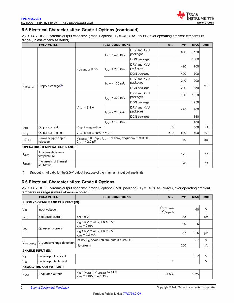
6.5 Electrical Characteristics: Grade 1 Options (continued)VIN = 14-V, 10-µF ceramic output capacitor, grade 1 options, TJ = –40°C to +150°C, over operating ambient temperature range (unless otherwise noted)
PARAMETER TEST CONDITIONS MIN TYP MAX UNIT
V(Dropout) Dropout voltage(1)
VOUT(NOM) = 5 V
IOUT = 300 mADRV and KVU packages 630 1170
mV
DGN package 1000
IOUT = 200 mADRV and KVU packages 420 780
DGN package 400 700
IOUT = 100 mADRV and KVU packages 210 390
DGN package 200 350
VOUT = 3.3 V
IOUT = 300 mADRV and KVU packages 730 1350
DGN package 1250
IOUT = 200 mADRV and KVU packages 475 900
DGN package 850
IOUT = 100 mA 450
IOUT Output current VOUT in regulation 0 300 mA
I(CL) Output current limit VOUT short to 90% × VOUT 310 510 690 mA
PSRR Power-supply ripple rejection
V(Ripple) = 0.5 VPP, IOUT = 10 mA, frequency = 100 Hz, COUT = 2.2 µF 60 dB
OPERATING TEMPERATURE RANGE
T(SD)Junction shutdown temperature 175 °C
T(HYST)Hysteresis of thermal shutdown 20 °C
(1) Dropout is not valid for the 2.5-V output because of the minimum input voltage limits.
6.6 Electrical Characteristics: Grade 0 OptionsVIN = 14-V, 10-µF ceramic output capacitor, grade 0 options (PWP package), TJ = –40°C to +165°C, over operating ambient temperature range (unless otherwise noted)
PARAMETER TEST CONDITIONS MIN TYP MAX UNITSUPPLY VOLTAGE AND CURRENT (IN)
VIN Input voltage VOUT(NOM) + V(Dropout)
40 V
I(SD) Shutdown current EN = 0 V 0.3 1 µA
I(Q) Quiescent current
VIN = 6 V to 40 V, EN ≥ 2 V,IOUT = 0 mA 1.9 5
VIN = 6 V to 40 V, EN ≥ 2 V,IOUT = 0.2 mA 2.7 6.5 µA
V(IN, UVLO) VIN undervoltage detectionRamp VIN down until the output turns OFF 2.7 V
Hysteresis 200 mV
ENABLE INPUT (EN)VIL Logic-input low level 0.7 V
VIH Logic-input high level 2 V
REGULATED OUTPUT (OUT)
VOUT Regulated output VIN = VOUT + V(Dropout) to 14 V,IOUT = 1 mA to 300 mA –1.5% 1.5%
TPS7B82-Q1SLVSDQ0I – SEPTEMBER 2017 – REVISED AUGUST 2021 www.ti.com
6 Submit Document Feedback Copyright © 2021 Texas Instruments Incorporated
Product Folder Links: TPS7B82-Q1

6.6 Electrical Characteristics: Grade 0 Options (continued)VIN = 14-V, 10-µF ceramic output capacitor, grade 0 options (PWP package), TJ = –40°C to +165°C, over operating ambient temperature range (unless otherwise noted)
PARAMETER TEST CONDITIONS MIN TYP MAX UNITV(Line-Reg) Line regulation VIN = 6 V to 40 V, IOUT = 10 mA 10 mV
V(Load-Reg) Load regulation VIN = 14 V, IOUT = 1 mA to 300 mA 20 mV
V(Dropout) Dropout voltage(1)
VOUT(NOM) = 5 V
IOUT = 300 mA 630 1170
mV
IOUT = 200 mA 420 780
IOUT = 100 mA 210 390
VOUT = 3.3 V
IOUT = 300 mA 730 1350
IOUT = 200 mA 475 900
IOUT = 100 mA 450
IOUT Output current VOUT in regulation 0 300 mA
I(CL) Output current limit VOUT short to 90% × VOUT 310 510 690 mA
PSRR Power-supply ripple rejection
V(Ripple) = 0.5 VPP, IOUT = 10 mA, frequency = 100 Hz, COUT = 2.2 µF 60 dB
OPERATING TEMPERATURE RANGE
T(SD)Junction shutdown temperature 185 °C
T(HYST)Hysteresis of thermal shutdown 20 °C
www.ti.comTPS7B82-Q1
SLVSDQ0I – SEPTEMBER 2017 – REVISED AUGUST 2021
Copyright © 2021 Texas Instruments Incorporated Submit Document Feedback 7
Product Folder Links: TPS7B82-Q1

6.7 Typical CharacteristicsVIN = 14 V, VEN ≥ 2 V, TJ = –40°C to 150°C (unless otherwise noted)
Output Current (mA)
Quie
scent
Curr
ent
(PA
)
0 50 100 150 200 250 3000
150
300
450
600
750
D001
�40°C25°C125°C
VOUT = 5 V
Figure 6-1. Quiescent Current vs Output Current
Input Voltage (V)
Quie
scent
Curr
ent
(PA
)
0 5 10 15 20 25 30 35 40-500
0
500
1000
1500
2000
2500
3000
D002
IOUT = 1 mAIOUT = 100 mAIOUT = 200 mA
VOUT = 5 V
Figure 6-2. Quiescent Current vs Input Voltage
Temperature (qC)
Shutd
ow
n C
urr
ent (P
A)
-40 -25 -10 5 20 35 50 65 80 95 110 1250
0.1
0.2
0.3
0.4
0.5
D003
VEN = 0 V
Figure 6-3. Shutdown Current vs Ambient Temperature
Temperature (°C)
Quie
scent
Curr
ent
(PA
)
-40 -25 -10 5 20 35 50 65 80 95 110 125-100
0
100
200
300
400
500
D004
IOUT = 1 mAIOUT = 100 mA
VOUT = 5 V
Figure 6-4. Quiescent Current vs Ambient Temperature
Output Current (mA)
Dro
pout
Voltage (
mV
)
0 50 100 150 200 250 3000
100
200
300
400
500
600
700
800
D005
�40°C25°C125°C
VIN = 5 V, 5-V fixed output, V(Dropout) = VIN – VOUT
Figure 6-5. Dropout Voltage vs Output Current
Temperature (qC)
Dro
pout V
oltage (
mV
)
-40 -25 -10 5 20 35 50 65 80 95 110 1250
100
200
300
400
500
600
700
800
D006
VIN = 5 V, 5-V fixed output, V(Dropout) = VIN – VOUT
Figure 6-6. Dropout Voltage vs Ambient Temperature
TPS7B82-Q1SLVSDQ0I – SEPTEMBER 2017 – REVISED AUGUST 2021 www.ti.com
8 Submit Document Feedback Copyright © 2021 Texas Instruments Incorporated
Product Folder Links: TPS7B82-Q1

6.7 Typical Characteristics (continued)VIN = 14 V, VEN ≥ 2 V, TJ = –40°C to 150°C (unless otherwise noted)
Temperature (qC)
Outp
ut
Voltag
e (
V)
-40 -25 -10 5 20 35 50 65 80 95 110 1254.9
4.95
5
5.05
5.1
D007
VOUT = 5 V
Figure 6-7. Output Voltage vs Ambient Temperature
Input Voltage (V)
Outp
ut
Voltage (
V)
0 5 10 15 20 25 30 35 40-0.5
0
0.5
1
1.5
2
2.5
3
3.5
4
4.5
5
5.5
D008
�40qC25qC125qC
VOUT = 5 V, IOUT = 1 mA
Figure 6-8. Output Voltage vs Input Voltage
Temperature (qC)
Curr
ent
Lim
it (
mA
)
-40 -25 -10 5 20 35 50 65 80 95 110 1250
100
200
300
400
500
600
700
D009
VIN = 14 V, VOUT is shorted to 90% × VOUT
Figure 6-9. Output Current Limit vs Ambient Temperature
Output Current (mA)
Load R
egula
tion (
%/m
A)
0 50 100 150 200 250 300-1
-0.8
-0.6
-0.4
-0.2
0
0.2
0.4
0.6
0.8
1
D010
�40°C25°C125°C
VOUT = 5 V
Figure 6-10. Load Regulation
Input Voltage (V)
Lin
e R
egula
tion (
%/V
)
0 5 10 15 20 25 30 35 40-1
-0.8
-0.6
-0.4
-0.2
0
0.2
0.4
0.6
0.8
1
D011
�40°C25°C125°C
VOUT = 5 V, IOUT = 10 mA
Figure 6-11. Line Regulation
Frequency (Hz)
PS
RR
(dB
)
-25
0
25
50
75
100
125
10 100 1k 10k 100k 1M 10M 100M
D012
IOUT = 10 mA
Figure 6-12. PSRR vs Frequency
www.ti.comTPS7B82-Q1
SLVSDQ0I – SEPTEMBER 2017 – REVISED AUGUST 2021
Copyright © 2021 Texas Instruments Incorporated Submit Document Feedback 9
Product Folder Links: TPS7B82-Q1

6.7 Typical Characteristics (continued)VIN = 14 V, VEN ≥ 2 V, TJ = –40°C to 150°C (unless otherwise noted)
Frequency (Hz)
PS
RR
(dB
)
-25
0
25
50
75
100
125
10 100 1k 10k 100k 1M 10M 100M
D013
IOUT = 100 mA
Figure 6-13. PSRR vs Frequency
ESR (:)
Outp
ut
Capacitance (P
F)
0.001 0.01 0.1 1 551
10
100
200
D014
Figure 6-14. Output Capacitance vs ESR Stability
TPS7B82-Q1SLVSDQ0I – SEPTEMBER 2017 – REVISED AUGUST 2021 www.ti.com
10 Submit Document Feedback Copyright © 2021 Texas Instruments Incorporated
Product Folder Links: TPS7B82-Q1
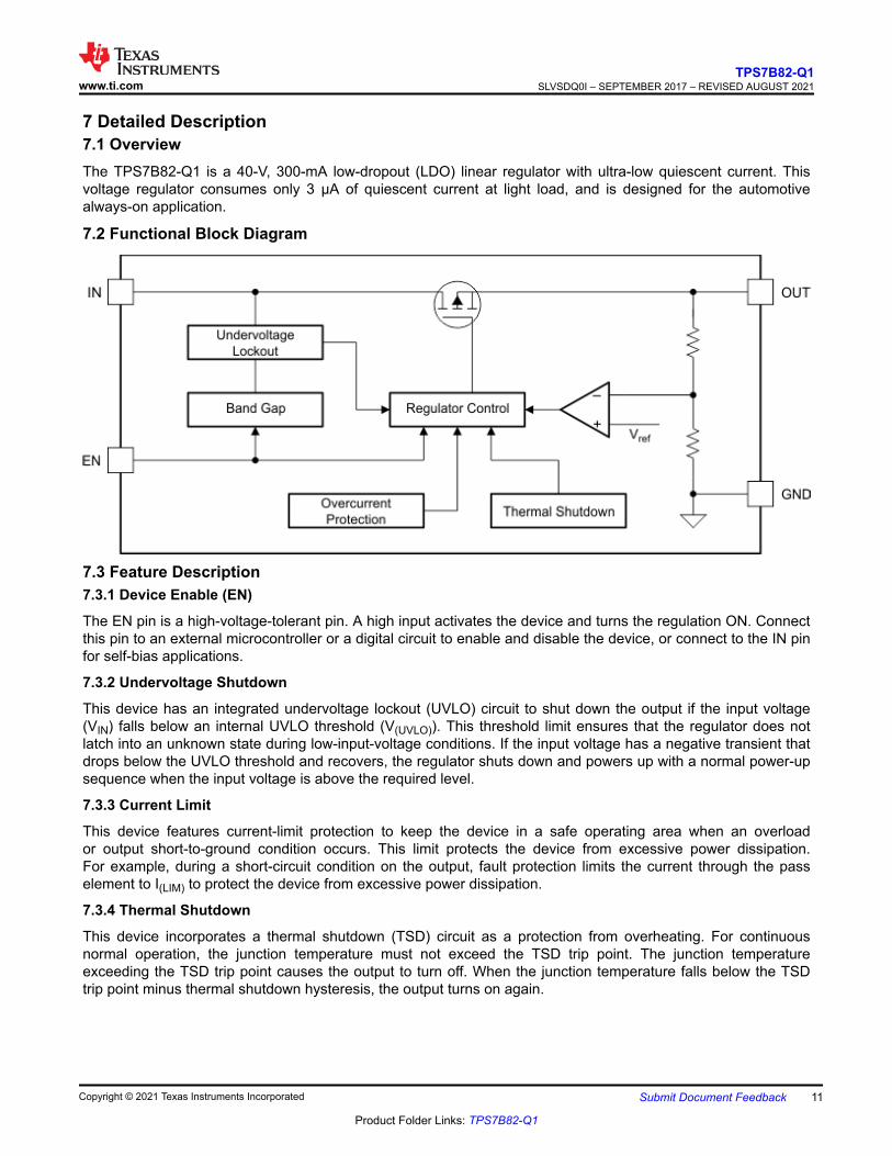
7 Detailed Description7.1 OverviewThe TPS7B82-Q1 is a 40-V, 300-mA low-dropout (LDO) linear regulator with ultra-low quiescent current. This voltage regulator consumes only 3 μA of quiescent current at light load, and is designed for the automotive always-on application.
7.2 Functional Block Diagram
7.3 Feature Description7.3.1 Device Enable (EN)
The EN pin is a high-voltage-tolerant pin. A high input activates the device and turns the regulation ON. Connect this pin to an external microcontroller or a digital circuit to enable and disable the device, or connect to the IN pin for self-bias applications.
7.3.2 Undervoltage Shutdown
This device has an integrated undervoltage lockout (UVLO) circuit to shut down the output if the input voltage (VIN) falls below an internal UVLO threshold (V(UVLO)). This threshold limit ensures that the regulator does not latch into an unknown state during low-input-voltage conditions. If the input voltage has a negative transient that drops below the UVLO threshold and recovers, the regulator shuts down and powers up with a normal power-up sequence when the input voltage is above the required level.
7.3.3 Current Limit
This device features current-limit protection to keep the device in a safe operating area when an overload or output short-to-ground condition occurs. This limit protects the device from excessive power dissipation. For example, during a short-circuit condition on the output, fault protection limits the current through the pass element to I(LIM) to protect the device from excessive power dissipation.
7.3.4 Thermal Shutdown
This device incorporates a thermal shutdown (TSD) circuit as a protection from overheating. For continuous normal operation, the junction temperature must not exceed the TSD trip point. The junction temperature exceeding the TSD trip point causes the output to turn off. When the junction temperature falls below the TSD trip point minus thermal shutdown hysteresis, the output turns on again.
www.ti.comTPS7B82-Q1
SLVSDQ0I – SEPTEMBER 2017 – REVISED AUGUST 2021
Copyright © 2021 Texas Instruments Incorporated Submit Document Feedback 11
Product Folder Links: TPS7B82-Q1

7.4 Device Functional Modes7.4.1 Operation With VIN Lower Than 3 V
The device normally operates with input voltages above 3 V. The device can also operate at lower input voltages; the maximum UVLO voltage is 2.7 V. At input voltages below the actual UVLO voltage, the device does not operate.
7.4.2 Operation With VIN Larger Than 3 V
When VIN is greater than 3 V, if VIN is also higher than the output set value plus the device dropout voltage, VOUT is equal to the set value. Otherwise, VOUT is equal to VIN minus the dropout voltage.
TPS7B82-Q1SLVSDQ0I – SEPTEMBER 2017 – REVISED AUGUST 2021 www.ti.com
12 Submit Document Feedback Copyright © 2021 Texas Instruments Incorporated
Product Folder Links: TPS7B82-Q1

8 Application and ImplementationNote
Information in the following applications sections is not part of the TI component specification, and TI does not warrant its accuracy or completeness. TI’s customers are responsible for determining suitability of components for their purposes, as well as validating and testing their design implementation to confirm system functionality.
8.1 Application InformationThe TPS7B82-Q1 is a 300-mA, 40-V low-dropout linear regulator with ultra-low quiescent current. The PSpice transient model is available for download on the product folder and can be used to evaluate the basic function of the device.
8.2 Typical ApplicationFigure 8-1 shows a typical application circuit for the TPS7B82-Q1. Different values of external components can be used, depending on the end application. An application may require a larger output capacitor during fast load steps to prevent a large drop on the output voltage. Use a low-ESR ceramic capacitor with a dielectric of type X5R or X7R.
Figure 8-1. TPS7B82-Q1 Typical Application Schematic
8.2.1 Design Requirements
For this design example, use the parameters listed in Table 8-1.
Table 8-1. Design Requirements ParametersPARAMETER VALUE
Input voltage range 3 V to 40 V
Output voltage 5 V or 3.3 V
Output current 300 mA maximum
8.2.2 Detailed Design Procedure
To begin the design process, determine the following:
• Input voltage range• Output voltage• Output current
www.ti.comTPS7B82-Q1
SLVSDQ0I – SEPTEMBER 2017 – REVISED AUGUST 2021
Copyright © 2021 Texas Instruments Incorporated Submit Document Feedback 13
Product Folder Links: TPS7B82-Q1

8.2.2.1 Input Capacitor
Although an input capacitor is not required for stability, good analog design practice is to connect a 10-µF to22-µF capacitor from IN to GND. This capacitor counteracts reactive input sources and improves transient response, input ripple rejection, and PSRR. The voltage rating must be greater than the maximum input voltage.
8.2.2.2 Output Capacitor
To ensure the stability of the TPS7B82-Q1, the device requires an output capacitor with a value in the range from 1 μF to 200 μF and with an ESR range between 0.001 Ω and 5 Ω. Select a ceramic capacitor with low ESR to improve the load transient response.
8.2.3 Application Curve
Figure 8-2. TPS7B82-Q1 Power-Up Waveform (5 V)
TPS7B82-Q1SLVSDQ0I – SEPTEMBER 2017 – REVISED AUGUST 2021 www.ti.com
14 Submit Document Feedback Copyright © 2021 Texas Instruments Incorporated
Product Folder Links: TPS7B82-Q1

9 Power Supply RecommendationsThe device is designed to operate from an input voltage supply range from 3 V to 40 V. This input supply must be well regulated. If the input supply is located more than a few inches from the TPS7B82-Q1, add a capacitor with a value greater than or equal to 10 μF with a 0.1-μF bypass capacitor in parallel at the input.
10 Layout10.1 Layout GuidelinesFor LDO power supplies, especially high-voltage and large output current supplies, layout is an important step. If layout is not carefully designed, the regulator can fail to deliver enough output current because of thermal limitation. To improve the thermal performance of the device, and to maximize the current output at high ambient temperature, spread the copper under the thermal pad as far as possible and place enough thermal vias on the copper under the thermal pad. Figure 10-1 shows an example layout.
10.2 Layout Example
IN
EN
GND
1
2
3
4
8
7
6
5
OUT
GND
Figure 10-1. TPSB82-Q1 Example Layout Diagram
www.ti.comTPS7B82-Q1
SLVSDQ0I – SEPTEMBER 2017 – REVISED AUGUST 2021
Copyright © 2021 Texas Instruments Incorporated Submit Document Feedback 15
Product Folder Links: TPS7B82-Q1

11 Device and Documentation Support11.1 Receiving Notification of Documentation UpdatesTo receive notification of documentation updates, navigate to the device product folder on ti.com. Click on Subscribe to updates to register and receive a weekly digest of any product information that has changed. For change details, review the revision history included in any revised document.
11.2 Support ResourcesTI E2E™ support forums are an engineer's go-to source for fast, verified answers and design help — straight from the experts. Search existing answers or ask your own question to get the quick design help you need.
Linked content is provided "AS IS" by the respective contributors. They do not constitute TI specifications and do not necessarily reflect TI's views; see TI's Terms of Use.
11.3 TrademarksPowerPAD™ and TI E2E™ are trademarks of Texas Instruments.All trademarks are the property of their respective owners.11.4 Electrostatic Discharge Caution
This integrated circuit can be damaged by ESD. Texas Instruments recommends that all integrated circuits be handled with appropriate precautions. Failure to observe proper handling and installation procedures can cause damage.ESD damage can range from subtle performance degradation to complete device failure. Precision integrated circuits may be more susceptible to damage because very small parametric changes could cause the device not to meet its published specifications.
11.5 GlossaryTI Glossary This glossary lists and explains terms, acronyms, and definitions.
12 Mechanical, Packaging, and Orderable InformationThe following pages include mechanical, packaging, and orderable information. This information is the most-current data available for the designated device. This data is subject to change without notice and without revision of this document. For browser-based versions of this data sheet, see the left-hand navigation pane.
TPS7B82-Q1SLVSDQ0I – SEPTEMBER 2017 – REVISED AUGUST 2021 www.ti.com
16 Submit Document Feedback Copyright © 2021 Texas Instruments Incorporated
Product Folder Links: TPS7B82-Q1

PACKAGE OPTION ADDENDUM
www.ti.com 20-Aug-2021
Addendum-Page 1
PACKAGING INFORMATION
Orderable Device Status(1)
Package Type PackageDrawing
Pins PackageQty
Eco Plan(2)
Lead finish/Ball material
(6)
MSL Peak Temp(3)
Op Temp (°C) Device Marking(4/5)
Samples
TPS7B8225QDGNRQ1 ACTIVE HVSSOP DGN 8 2500 RoHS & Green NIPDAUAG Level-2-260C-1 YEAR -40 to 150 1QFX
TPS7B8233EPWPRQ1 ACTIVE HTSSOP PWP 14 2500 RoHS & Green NIPDAU Level-3-260C-168 HR -40 to 150 7B8233E
TPS7B8233QDGNRQ1 ACTIVE HVSSOP DGN 8 2500 RoHS & Green NIPDAUAG Level-2-260C-1 YEAR -40 to 150 1GGX
TPS7B8233QDRVRQ1 ACTIVE WSON DRV 6 3000 RoHS & Green NIPDAU Level-2-260C-1 YEAR -40 to 150 1ORH
TPS7B8233QKVURQ1 ACTIVE TO-252 KVU 5 2500 RoHS & Green SN Level-3-260C-168 HR -40 to 150 7B8233Q1
TPS7B8250EPWPRQ1 ACTIVE HTSSOP PWP 14 2500 RoHS & Green NIPDAU Level-3-260C-168 HR -40 to 150 7B8250E
TPS7B8250QDGNRQ1 ACTIVE HVSSOP DGN 8 2500 RoHS & Green NIPDAUAG Level-2-260C-1 YEAR -40 to 150 19TX
TPS7B8250QDRVRQ1 ACTIVE WSON DRV 6 3000 RoHS & Green NIPDAU Level-2-260C-1 YEAR -40 to 150 1UFH
TPS7B8250QKVURQ1 ACTIVE TO-252 KVU 5 2500 RoHS & Green SN Level-3-260C-168 HR -40 to 150 7B8250Q1
(1) The marketing status values are defined as follows:ACTIVE: Product device recommended for new designs.LIFEBUY: TI has announced that the device will be discontinued, and a lifetime-buy period is in effect.NRND: Not recommended for new designs. Device is in production to support existing customers, but TI does not recommend using this part in a new design.PREVIEW: Device has been announced but is not in production. Samples may or may not be available.OBSOLETE: TI has discontinued the production of the device.
(2) RoHS: TI defines "RoHS" to mean semiconductor products that are compliant with the current EU RoHS requirements for all 10 RoHS substances, including the requirement that RoHS substancedo not exceed 0.1% by weight in homogeneous materials. Where designed to be soldered at high temperatures, "RoHS" products are suitable for use in specified lead-free processes. TI mayreference these types of products as "Pb-Free".RoHS Exempt: TI defines "RoHS Exempt" to mean products that contain lead but are compliant with EU RoHS pursuant to a specific EU RoHS exemption.Green: TI defines "Green" to mean the content of Chlorine (Cl) and Bromine (Br) based flame retardants meet JS709B low halogen requirements of <=1000ppm threshold. Antimony trioxide basedflame retardants must also meet the <=1000ppm threshold requirement.
(3) MSL, Peak Temp. - The Moisture Sensitivity Level rating according to the JEDEC industry standard classifications, and peak solder temperature.
(4) There may be additional marking, which relates to the logo, the lot trace code information, or the environmental category on the device.

PACKAGE OPTION ADDENDUM
www.ti.com 20-Aug-2021
Addendum-Page 2
(5) Multiple Device Markings will be inside parentheses. Only one Device Marking contained in parentheses and separated by a "~" will appear on a device. If a line is indented then it is a continuationof the previous line and the two combined represent the entire Device Marking for that device.
(6) Lead finish/Ball material - Orderable Devices may have multiple material finish options. Finish options are separated by a vertical ruled line. Lead finish/Ball material values may wrap to twolines if the finish value exceeds the maximum column width.
Important Information and Disclaimer:The information provided on this page represents TI's knowledge and belief as of the date that it is provided. TI bases its knowledge and belief on informationprovided by third parties, and makes no representation or warranty as to the accuracy of such information. Efforts are underway to better integrate information from third parties. TI has taken andcontinues to take reasonable steps to provide representative and accurate information but may not have conducted destructive testing or chemical analysis on incoming materials and chemicals.TI and TI suppliers consider certain information to be proprietary, and thus CAS numbers and other limited information may not be available for release.
In no event shall TI's liability arising out of such information exceed the total purchase price of the TI part(s) at issue in this document sold by TI to Customer on an annual basis.

TAPE AND REEL INFORMATION
*All dimensions are nominal
Device PackageType
PackageDrawing
Pins SPQ ReelDiameter
(mm)
ReelWidth
W1 (mm)
A0(mm)
B0(mm)
K0(mm)
P1(mm)
W(mm)
Pin1Quadrant
TPS7B8225QDGNRQ1 HVSSOP DGN 8 2500 330.0 12.4 5.3 3.4 1.4 8.0 12.0 Q1
TPS7B8233EPWPRQ1 HTSSOP PWP 14 2500 330.0 12.4 6.9 5.6 1.6 8.0 12.0 Q1
TPS7B8233QDGNRQ1 HVSSOP DGN 8 2500 330.0 12.4 5.3 3.4 1.4 8.0 12.0 Q1
TPS7B8233QDRVRQ1 WSON DRV 6 3000 180.0 8.4 2.3 2.3 1.15 4.0 8.0 Q2
TPS7B8233QKVURQ1 TO-252 KVU 5 2500 330.0 16.4 6.9 10.5 2.7 8.0 16.0 Q2
TPS7B8250EPWPRQ1 HTSSOP PWP 14 2500 330.0 12.4 6.9 5.6 1.6 8.0 12.0 Q1
TPS7B8250QDGNRQ1 HVSSOP DGN 8 2500 330.0 12.4 5.3 3.4 1.4 8.0 12.0 Q1
TPS7B8250QDRVRQ1 WSON DRV 6 3000 180.0 8.4 2.3 2.3 1.15 4.0 8.0 Q2
TPS7B8250QKVURQ1 TO-252 KVU 5 2500 330.0 16.4 6.9 10.5 2.7 8.0 16.0 Q2
PACKAGE MATERIALS INFORMATION
www.ti.com 25-Nov-2021
Pack Materials-Page 1

*All dimensions are nominal
Device Package Type Package Drawing Pins SPQ Length (mm) Width (mm) Height (mm)
TPS7B8225QDGNRQ1 HVSSOP DGN 8 2500 366.0 364.0 50.0
TPS7B8233EPWPRQ1 HTSSOP PWP 14 2500 853.0 449.0 35.0
TPS7B8233QDGNRQ1 HVSSOP DGN 8 2500 366.0 364.0 50.0
TPS7B8233QDRVRQ1 WSON DRV 6 3000 210.0 185.0 35.0
TPS7B8233QKVURQ1 TO-252 KVU 5 2500 340.0 340.0 38.0
TPS7B8250EPWPRQ1 HTSSOP PWP 14 2500 853.0 449.0 35.0
TPS7B8250QDGNRQ1 HVSSOP DGN 8 2500 366.0 364.0 50.0
TPS7B8250QDRVRQ1 WSON DRV 6 3000 210.0 185.0 35.0
TPS7B8250QKVURQ1 TO-252 KVU 5 2500 340.0 340.0 38.0
PACKAGE MATERIALS INFORMATION
www.ti.com 25-Nov-2021
Pack Materials-Page 2
GENERIC PACKAGE VIEW
Images above are just a representation of the package family, actual package may vary.Refer to the product data sheet for package details.
DRV 6 WSON - 0.8 mm max heightPLASTIC SMALL OUTLINE - NO LEAD
4206925/F

www.ti.com
PACKAGE OUTLINE
C
6X 0.350.25
1.6 0.1
6X 0.30.2
2X1.3
1 0.1
4X 0.65
0.80.7
0.050.00
B 2.11.9
A
2.11.9
(0.2) TYP
WSON - 0.8 mm max heightDRV0006APLASTIC SMALL OUTLINE - NO LEAD
4222173/B 04/2018
PIN 1 INDEX AREA
SEATING PLANE
0.08 C
1
34
6
(OPTIONAL)PIN 1 ID
0.1 C A B0.05 C
THERMAL PADEXPOSED
7
NOTES: 1. All linear dimensions are in millimeters. Any dimensions in parenthesis are for reference only. Dimensioning and tolerancing per ASME Y14.5M. 2. This drawing is subject to change without notice. 3. The package thermal pad must be soldered to the printed circuit board for thermal and mechanical performance.
SCALE 5.500

www.ti.com
EXAMPLE BOARD LAYOUT
0.07 MINALL AROUND
0.07 MAXALL AROUND
(1)
4X (0.65)
(1.95)
6X (0.3)
6X (0.45)
(1.6)
(R0.05) TYP
( 0.2) VIATYP
(1.1)
WSON - 0.8 mm max heightDRV0006APLASTIC SMALL OUTLINE - NO LEAD
4222173/B 04/2018
SYMM
1
34
6
SYMM
LAND PATTERN EXAMPLESCALE:25X
7
NOTES: (continued) 4. This package is designed to be soldered to a thermal pad on the board. For more information, see Texas Instruments literature number SLUA271 (www.ti.com/lit/slua271).5. Vias are optional depending on application, refer to device data sheet. If some or all are implemented, recommended via locations are shown.
SOLDER MASKOPENINGSOLDER MASK
METAL UNDER
SOLDER MASKDEFINED
METALSOLDER MASKOPENING
SOLDER MASK DETAILS
NON SOLDER MASKDEFINED
(PREFERRED)

www.ti.com
EXAMPLE STENCIL DESIGN
6X (0.3)
6X (0.45)
4X (0.65)
(0.7)
(1)
(1.95)
(R0.05) TYP
(0.45)
WSON - 0.8 mm max heightDRV0006APLASTIC SMALL OUTLINE - NO LEAD
4222173/B 04/2018
NOTES: (continued) 6. Laser cutting apertures with trapezoidal walls and rounded corners may offer better paste release. IPC-7525 may have alternate design recommendations.
SOLDER PASTE EXAMPLEBASED ON 0.125 mm THICK STENCIL
EXPOSED PAD #7
88% PRINTED SOLDER COVERAGE BY AREA UNDER PACKAGESCALE:30X
SYMM
1
3 4
6
SYMM
METAL7


www.ti.com
GENERIC PACKAGE VIEW
This image is a representation of the package family, actual package may vary.Refer to the product data sheet for package details.
PowerPAD VSSOP - 1.1 mm max heightDGN 8SMALL OUTLINE PACKAGE3 x 3, 0.65 mm pitch
4225482/A

www.ti.com
PACKAGE OUTLINE
C
6X 0.65
2X1.95
8X 0.380.25
5.054.75 TYP
SEATINGPLANE
0.150.05
0.25GAGE PLANE
0 -8
1.1 MAX
0.230.13
1.8461.646
2.151.95
B 3.12.9
NOTE 4
A
3.12.9
NOTE 3
0.70.4
PowerPAD VSSOP - 1.1 mm max heightDGN0008GSMALL OUTLINE PACKAGE
4225480/A 11/2019
1
4
5
8
0.13 C A B
PIN 1 INDEX AREA
SEE DETAIL A
0.1 C
NOTES: 1. All linear dimensions are in millimeters. Any dimensions in parenthesis are for reference only. Dimensioning and tolerancing per ASME Y14.5M. 2. This drawing is subject to change without notice. 3. This dimension does not include mold flash, protrusions, or gate burrs. Mold flash, protrusions, or gate burrs shall not exceed 0.15 mm per side. 4. This dimension does not include interlead flash. Interlead flash shall not exceed 0.25 mm per side.5. Reference JEDEC registration MO-187.
PowerPAD is a trademark of Texas Instruments.
TM
A 20DETAIL ATYPICAL
SCALE 4.000
EXPOSED THERMAL PAD
1
45
8
9
www.ti.com
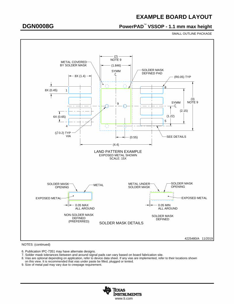
EXAMPLE BOARD LAYOUT
0.05 MAXALL AROUND
0.05 MINALL AROUND
8X (1.4)
8X (0.45)
6X (0.65)
(4.4)
(R0.05) TYP
(2)NOTE 9
(3)NOTE 9
(1.22)
(0.55)( 0.2) TYP
VIA
(1.846)
(2.15)
PowerPAD VSSOP - 1.1 mm max heightDGN0008GSMALL OUTLINE PACKAGE
4225480/A 11/2019
NOTES: (continued) 6. Publication IPC-7351 may have alternate designs. 7. Solder mask tolerances between and around signal pads can vary based on board fabrication site.8. Vias are optional depending on application, refer to device data sheet. If any vias are implemented, refer to their locations shown on this view. It is recommended that vias under paste be filled, plugged or tented.9. Size of metal pad may vary due to creepage requirement.
TM
LAND PATTERN EXAMPLEEXPOSED METAL SHOWN
SCALE: 15X
SYMM
SYMM
1
4
5
8
SOLDER MASKDEFINED PAD
METAL COVEREDBY SOLDER MASK
SEE DETAILS
9
15.000
METALSOLDER MASKOPENING
METAL UNDERSOLDER MASK
SOLDER MASKOPENING
EXPOSED METALEXPOSED METAL
SOLDER MASK DETAILS
NON-SOLDER MASKDEFINED
(PREFERRED)
SOLDER MASKDEFINED
www.ti.com
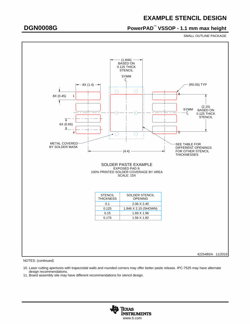
EXAMPLE STENCIL DESIGN
8X (1.4)
8X (0.45)
6X (0.65)
(4.4)
(R0.05) TYP
(1.846)BASED ON
0.125 THICKSTENCIL
(2.15)BASED ON
0.125 THICKSTENCIL
PowerPAD VSSOP - 1.1 mm max heightDGN0008GSMALL OUTLINE PACKAGE
4225480/A 11/2019
1.56 X 1.820.1751.69 X 1.960.15
1.846 X 2.15 (SHOWN)0.1252.06 X 2.400.1
SOLDER STENCILOPENING
STENCILTHICKNESS
NOTES: (continued) 10. Laser cutting apertures with trapezoidal walls and rounded corners may offer better paste release. IPC-7525 may have alternate design recommendations. 11. Board assembly site may have different recommendations for stencil design.
TM
SOLDER PASTE EXAMPLEEXPOSED PAD 9:
100% PRINTED SOLDER COVERAGE BY AREASCALE: 15X
SYMM
SYMM
1
4 5
8
METAL COVEREDBY SOLDER MASK
SEE TABLE FORDIFFERENT OPENINGSFOR OTHER STENCILTHICKNESSES

IMPORTANT NOTICE AND DISCLAIMERTI PROVIDES TECHNICAL AND RELIABILITY DATA (INCLUDING DATA SHEETS), DESIGN RESOURCES (INCLUDING REFERENCE DESIGNS), APPLICATION OR OTHER DESIGN ADVICE, WEB TOOLS, SAFETY INFORMATION, AND OTHER RESOURCES “AS IS” AND WITH ALL FAULTS, AND DISCLAIMS ALL WARRANTIES, EXPRESS AND IMPLIED, INCLUDING WITHOUT LIMITATION ANY IMPLIED WARRANTIES OF MERCHANTABILITY, FITNESS FOR A PARTICULAR PURPOSE OR NON-INFRINGEMENT OF THIRD PARTY INTELLECTUAL PROPERTY RIGHTS.These resources are intended for skilled developers designing with TI products. You are solely responsible for (1) selecting the appropriate TI products for your application, (2) designing, validating and testing your application, and (3) ensuring your application meets applicable standards, and any other safety, security, regulatory or other requirements.These resources are subject to change without notice. TI grants you permission to use these resources only for development of an application that uses the TI products described in the resource. Other reproduction and display of these resources is prohibited. No license is granted to any other TI intellectual property right or to any third party intellectual property right. TI disclaims responsibility for, and you will fully indemnify TI and its representatives against, any claims, damages, costs, losses, and liabilities arising out of your use of these resources.TI’s products are provided subject to TI’s Terms of Sale or other applicable terms available either on ti.com or provided in conjunction with such TI products. TI’s provision of these resources does not expand or otherwise alter TI’s applicable warranties or warranty disclaimers for TI products.TI objects to and rejects any additional or different terms you may have proposed. IMPORTANT NOTICE
Mailing Address: Texas Instruments, Post Office Box 655303, Dallas, Texas 75265Copyright © 2021, Texas Instruments Incorporated