tpu2000//2000r modbus/modbus plus … · tpu2000/2000r modbus/modbus plus automation guide i...
TRANSCRIPT
TPU2000/2000R Modbus/Modbus Plus Automation Guide
i
TPU2000//2000R MODBUS/MODBUS PLUSAUTOMATION TECHNICAL GUIDE
TG 7.11.1.7-61
Version 1.0
12/01
TPU2000/2000R Modbus/Modbus Plus Automation Guide
ii
ContentsSection 1 – IntroductionIntroduction .................................................................................................................................................... 1
Section 2 – Communication Card Identification and Physical Port CharacteristicsCommunication Identification and Physical Port Characteristics......................................................................... 3Communication Card Part Number Options ...................................................................................................... 5Unit Communication Card Verification .............................................................................................................. 8
Section 3 – TPU2000 and TPU2000R Device ConnectivityTPU2000 and TPU2000R Device Connectivity............................................................................................... 10RS232 Interface Connectivity ........................................................................................................................ 10Port Isolation ................................................................................................................................................ 10RS232 Handshaking Defined......................................................................................................................... 11RS232 Cable Connectivity ............................................................................................................................ 11RS485 Device Connectivity with the TPU2000 and TPU2000R........................................................................ 13
Section 4 – TPU2000 and TPU2000R Device ParameterizationTPU2000 and TPU2000R Device Parameterization ........................................................................................ 17COM 0 Port (Front Port Configuration) ........................................................................................................... 17COM Port 1 Option Settings (TPU2000R Only) [Catalog 588XXX00-XXX0 or 588XXX50-XXX0] ....................... 19COM Port 2 Option Settings (TPU2000R Only) [Catalog 588XXX00-XXX0 or 588XXXX6-XXX4] ....................... 20COM Port 3 and AUX COM Configuration ...................................................................................................... 21Modbus Protocol Selection and Configuration for Port 3 and AUX COM ........................................................... 22Modbus Plus Port Configuration [COM 3 on Selected Units] (TPU2000R Only)................................................. 24IRIG B Configuration and Wiring.................................................................................................................... 24Hardware Configuration ................................................................................................................................ 27Software Configuration.................................................................................................................................. 29
Section 5 – ModbusModbus Protocol........................................................................................................................................... 30Modbus ASCII Emulation .............................................................................................................................. 30Modbus RTU Emulation................................................................................................................................ 32Modbus Plus (Available on the TPU2000R Only) ............................................................................................ 33Modbus Plus Theory of Operation.................................................................................................................. 33Modbus and Modbus Plus General Notes....................................................................................................... 37Modbus/Modbus Plus Register Map............................................................................................................... 370X Discrete Coils.......................................................................................................................................... 37Function Code 1 (Read Coil Status) – Read Only Data.................................................................................... 38Modbus 0X Implementation Features ............................................................................................................. 39Logical Output Block (Single Bit Data) – 108 Discrete Coils (99 Elements Defined for 2 Winding TPU, 176
Elements Defined for 3 Winding TPU) ................................................................................................ 41Physical Output Block (Single Bit Data) – 16 Discrete Coils (8 Elements Defined)............................................. 50Logical Output Block (Two Bit Data with Momentary Change Detection)........................................................... 50Physical Output Block (Two Bit Data with Momentary Change Detection): Not available on TPU2000 ................ 541X Discrete Contact Inputs............................................................................................................................ 55Function Code 2 – Read Input Status (Read Only Data).................................................................................. 55Logical Inputs (34 Elements Defined 2 Winding TPU2000/2000R – 80 Elements Defined 3 Winding
TPU2000/2000R).............................................................................................................................. 57Physical Inputs (16 Elements Defined) ........................................................................................................... 59Momentary Change Detect Logical Inputs (68 Elements Defined 2 Winding TPU – 160 Elements Defined 3
Winding TPU)................................................................................................................................... 59Physical Input Momentary Change Detect (32 Elements Defined).................................................................... 634X Register Read Capabilities ....................................................................................................................... 64
TPU2000/2000R Modbus/Modbus Plus Automation Guide
iii
Function Code 03 – Read Holding Registers (Read Only) ............................................................................... 66Register Scaling and Re-Mapping and User Definable (UDR) Configuraton Process......................................... 66TPU2000 and TPU2000R Internal Operation.................................................................................................. 67ABB Data Type Definitions ............................................................................................................................ 68Register Scaling Investigated ........................................................................................................................ 69Scaling Option and Destination Register Length Options Explained ................................................................. 70Destination Register Length Justification Options Explained ............................................................................ 73Source Register Address and Source Register Type Explained ....................................................................... 73Source Scale Range and Source Scale Type Selections Explained.................................................................. 73TPU2000 and TPU2000R User Definable Register Defaults............................................................................ 75Relay Status (1 Register Defined).................................................................................................................. 78Diagnostic Status (2 Registers Defined)......................................................................................................... 79Unit Information (15 Registers Defined).......................................................................................................... 80Read Quick Status (3 Registers Defined) ....................................................................................................... 81Power Fail Status Information (9 Registers Defined) ....................................................................................... 82Fast Status (2 Registers Defined) .................................................................................................................. 82Communication Event Log (8 Registers Defined) ............................................................................................ 83Metering Values (35 Registers Defined)......................................................................................................... 84Load Current and Angular Values (63 Registers Defined TPU 2 Winding– 66 Registers Defined
TPU 3 Winding) ................................................................................................................................ 85RMS Voltage/Angular/Real and Reactive Power/Energy Values Block (17 Registers Defined) ........................... 87RMS Demand Current/Real and Reactive Power Values Block (24 Registers Defined)...................................... 88Minimum and Maximum Peak Demand (60 Registers Defined)........................................................................ 89Breaker Counters (11 Registers Defined) Modbus Function 03 Read Only ....................................................... 96Discrete 4X Register Bit Data Reporting (26 Registers Defined)....................................................................... 974X Register Write Capabilities ......................................................................................................................106Function Code 16 Preset 4X Registers (Write Only).......................................................................................107Function Code 23 Read/Write Register (Read/Write Concurrently)..................................................................108Fault Records ..............................................................................................................................................108Differential Fault Record Reporting ...............................................................................................................110Through Fault Buffers ..................................................................................................................................114Harmonic Restraint Fault Record ..................................................................................................................118Event Records (11 Registers Defined) ..........................................................................................................123Providing Control Functionality in the TPU2000/2000R...................................................................................126Group I Control Features Explained..............................................................................................................129Scada Redi .................................................................................................................................................130Group II Control Features Explained.............................................................................................................132Group III Control Features Explained ............................................................................................................136Group IV Control Features Explained............................................................................................................139Group V Control Features Explained.............................................................................................................145Group VI Control Features Explained............................................................................................................149Oscillographic Data Storage (Version 1.5 and Greater TPU2000R Only).........................................................151Oscillographic Configuration (12 Registers Defined).......................................................................................152Oscillographic Data Retrieval........................................................................................................................155Data Retrieval Theory of Operation...............................................................................................................155Oscillographic Data Interpretation .................................................................................................................1646X Registers ...............................................................................................................................................165Function Code 20 (Read General Reference) and 21 (Write General Reference).............................................166Programmable Input Configuration................................................................................................................167Term Definitions ..........................................................................................................................................167Methodology and Register Manipulation to Configure the Programmable Logical Input ....................................168Programmable Output Select Configuration...................................................................................................174Programmable Output User Defined String Block...........................................................................................178Settings ......................................................................................................................................................179Configuration Settings..................................................................................................................................194Counters .....................................................................................................................................................197Alarm Settings .............................................................................................................................................197Real Time Clock (13 Registers Defined)........................................................................................................199ULO Connection Settings and User Names ...................................................................................................199
TPU2000/2000R Modbus/Modbus Plus Automation Guide
iv
ULI Connection Settings and User Names.....................................................................................................201Force Logical Input Allocation and Name Assignment ....................................................................................202Modbus Plus Global Register Mapping (37 Registers Defined) TPU2000R Only ..............................................205User Definable Register Configuration Block .................................................................................................209Modbus ASCII Communication Test Example................................................................................................225Calculation of the LRC (Longitudinal Redundancy Code)................................................................................226Modbus CRC-16 Calculation ........................................................................................................................226TPU2000/TPU2000R Modbus Exception Response Analysis .........................................................................227Modbus Troubleshooting Tips.......................................................................................................................228TPU2000/TPU2000R Modbus ASCII Communication Timing Analysis ............................................................229Modbus Baud Rate Analysis ........................................................................................................................230TPU2000/TPU2000R Throughput Analysis....................................................................................................232Final Throughput Calculation and Analysis....................................................................................................232Modbus Plus Troubleshooting.......................................................................................................................234Modbus Plus Throughput .............................................................................................................................235
Appendix A-TPU Standard 10 Byte Protocol Document..................................................................................237Appendix B-ASCII Conversion Table.............................................................................................................328Appendix C-Modbus Plus Communication Between an ABB Protective Relay and a Modicon PLC ...................331Appendix D-Telebyte RS232/485 Converter Connection to ABB Protective Relays ..........................................338
The following are trademarks of AEG Schneider Automation Inc.Modbus, Modbus Plus, ModiconIBM, OS 2, and IBM PC are registered trademarks of International Business Machines Corporation.The following are registered trademarks of the Microsoft Corporation:Windows NT Windows 3.1Windows 95 Windows 98Hyperterminal MS-DOSMicrosoft USDATA is a registered trademark of the USDATA Corporation.
TPU2000/2000R Modbus/Modbus Plus Automation Guide
v
TablesSection 1 – IntroductionTable 1-1. Protocol Capabilities Listed by Product Type ................................................................................... 2
Section 2 – Communication Card Identification and Physical Port CharacteristicsTable 2-1. TPU2000 Communication Options .................................................................................................. 6Table 2-2. TPU2000 Communication Card Matrix for Unit 488MRXDZ-CSSSQ.................................................. 7Table 2-3. TPU2000R Communication Options................................................................................................ 7Table 2-4. TPU2000R Communication Card Matrix for Unit 588XXXYZ-XXXXQ ................................................ 8Table 2-5. TPU2000R Communication Card Matrix......................................................................................... 8
Section 3 – TPU2000 and TPU2000R Device ConnectivityTable 3-1. Physical Interface Options ............................................................................................................ 10Table 3-2. TPU2000 AUX COM Signal Assignments...................................................................................... 16
Section 4 – TPU2000 and TPU2000R Device ParameterizationTable 4-1. TPU2000 and TPU2000R COM Port 0 Front Panel Interface Parameters ........................................ 17Table 4-2. WinECP Communication Port Settings .......................................................................................... 19Table 4-3. COM Port 1 and COM Port 2 WinECP Port Setting Options............................................................ 19Table 4-4. Valid Parameter Selection for Standard Ten Byte and Modbus Protocols ........................................ 22
Section 5 – ModbusTable 5-1. Logical Output Modbus Address Map Definition ............................................................................. 41Table 5-2. Physical Output Contact Mapping Defined..................................................................................... 50Table 5-3. Momentary Change Detect Data Definition .................................................................................... 50Table 5-4. Modbus Physical Output Momentary Change Detect Address Allocation ......................................... 54Table 5-5. Logical Input Modbus Address Map Definition................................................................................ 57Table 5-6. Physical Input Modbus Address Map Definition.............................................................................. 59Table 5-7. Logical Input Status Momentary Change Detect Status .................................................................. 59Table 5-8. Physical Input Momentary Change Detect Register Map ................................................................ 63Table 5-9. Register Scaling Queries .............................................................................................................. 69Table 5-10. Minimum and Maximum Ranges for Scaled Numbers Depending Upon Scale Option and
Bit Length Selected........................................................................................................................... 71Table 5-11. Default Scaling and Remapping Register Assignments ................................................................ 75Table 5-12. Relay Status Modbus Address Map Definition.............................................................................. 78Table 5-13. Diagnostic Status Modbus Address Map Definition....................................................................... 80Table 5-14. Unit Information Status Modbus Address Map Definition............................................................... 81Table 5-15. Quick Status Modbus Address Map Definition.............................................................................. 82Table 5-16. Power Fail Table Register Definition............................................................................................ 82Table 5-17. Fast Status Modbus Address Map Definition................................................................................ 83Table 5-18. Communication Error Event Log ................................................................................................. 83Table 5-19. TPU2000/TPU2000R Metering Values ........................................................................................ 84Table 5-20. Demand Metering Modbus Address Map Definition...................................................................... 85Table 5-21. TPU2000/TPU2000R Metering Values ........................................................................................ 87Table 5-22. To Be Named ............................................................................................................................ 88Table 5-23. Peak Demand Register Map for the TPU2000R and TPU2000...................................................... 90Table 5-24. Minimum Demand Register Map for the TPU2000R and TPU2000................................................ 93Table 5-25. Breaker Counter Definition Table ................................................................................................ 96Table 5-26. Logical Input Table (8 Registers 128 Elements) ........................................................................... 97Table 5-27. Logical Input Definition Table (8 Registers – 127 Elements).........................................................100Table 5-28. Physical Output Table (1 Register Defined).................................................................................102Table 5-29. Physical Input Table (1 Register Defined) ...................................................................................102Table 5-30. Force Table Mapping ................................................................................................................103Table 5-31. Three Winding Logical Output Points .........................................................................................105Table 5-32. Fault Record Data Assignment ..................................................................................................109
TPU2000/2000R Modbus/Modbus Plus Automation Guide
vi
Table 5-33. Differential 2 Winding Fault Record Register Definition ................................................................110Table 5-34. 2 Winding Differential Fault Record Address Table......................................................................113Table 5-35. 2 Winding Through Fault Register Definition for the TPU2000/TPU2000R ....................................115Table 5-36. 3 Winding Through Fault Record Buffer Modbus Register Definition.............................................117Table 5-37. 2 Winding Harmonic Restraint Fault Record Buffer Modbus Register Assignment .........................119Table 5-38. 3 Winding Harmonic Fault Register Definitions............................................................................121Table 5-39. Operation Record Address Definition..........................................................................................124Table 5-40. Event Record Definition Type.....................................................................................................124Table 5-41. Security Status Register Indicating Password Requirement .........................................................127Table 5-42. Group I Control Registers ..........................................................................................................129Table 5-43. Group II Bit Definitions for TPU2000R Control.............................................................................133Table 5-44. State Truth Chart for Physical Input Forcing Function ..................................................................134Table 5-45. TPU2000R Bit Control Function Definitions.................................................................................136Table 5-46. State Truth Chart for Physical Input Forcing Function ..................................................................138Table 5-47. ECP Default Correlation to Forced Logical Input Bit Map .............................................................140Table 5-48. State Truth Chart for Physical Input Forcing Function ..................................................................142Table 5-49. TPU2000 and TPU2000R Bit Control Function Definitions ...........................................................142Table 5-50. State Truth Chart for Physical Input Forcing Function ..................................................................145Table 5-51. TPU2000 and TPU2000R Bit Control Function Definitions ...........................................................145Table 5-52. TPU2000 and TPU2000R Bit Control Function Definitions ...........................................................150Table 5-53. Oscillographic Resolution Capabilities ........................................................................................152Table 5-54. Oscillographic Configuration Registers .......................................................................................153Table 5-55. Oscillographic Data Format Retrieval Block ................................................................................156Table 5-56. Physical Logical Function Byte Configuration Codes for Register 60044 to 60058 .........................169Table 5-57. Relay Configuration Setting Definition ........................................................................................170Table 5-58. Programmable Input “NEGATED” “AND” Input ............................................................................171Table 5-59. AND/OR Conditional Logic Table ...............................................................................................172Table 5-60. Physical Input Mapping Table ....................................................................................................173Table 5-61. Relay Configuration Setting Definition ........................................................................................174Table 5-62. Physical Logical Function Byte Configuration Codes for Register 60044 to 60058 .........................175Table 5-63. Programmable Output AND/OR Select.......................................................................................178Table 5-64. Programmable Output User Defined Strings ...............................................................................178Table 5-65. To Be Named ...........................................................................................................................179Table 5-66. Primary Settings Register Definition Common to the 2 and 3 Winding Units..................................180Table 5-67. 3 Winding Primary Settings Block ..............................................................................................183Table 5-68. ALT 1 Settings Register Definition..............................................................................................185Table 5-69. Alternate 1 Settings for 3 Winding Block.....................................................................................188Table 5-70. ALT 2 Settings Register Definition..............................................................................................190Table 5-71. Alternate 2 Settings for 3 Winding Block.....................................................................................193Table 5-72. TPU2000/2000R Configuration Settings Register Setting.............................................................194Table 5-73. TPU2000/2000R Configuration Settings Register Setting.............................................................196Table 5-74. Counter Register Assignment ....................................................................................................197Table 5-75. Alarm Setting Table...................................................................................................................198Table 5-76. 3 Winding Alarm Settings Block .................................................................................................198Table 5-77. Real Time Clock Register Definition Assignment .........................................................................199Table 5-78. ULO Table Map for Character Name Assignment........................................................................199Table 5-79. ULI Table Map for Character Name Assignment .........................................................................201Table 5-80. FLI Soft Bit Table Map and Character Name Assignment Register Map........................................202Table 5-81. Modbus Plus Global Register Map Configuration Definition..........................................................207Table 5-82. User Definable Register Configuration Table ..............................................................................210Table 5-83. Modbus Standard Exception Codes ...........................................................................................228Table 5-84. TPU2000/TPU2000R Defined Exception Codes..........................................................................228Table 5-85. Character Transfer Time vs Baud Rate.......................................................................................231Table 5-86. TPU2000/TPU2000R Modbus CommandThroughput (Average time in mS)..................................232
TPU2000/2000R Modbus/Modbus Plus Automation Guide
vii
FiguresSection 1 – IntroductionFigure 1-1. Distribution Protection Unit Product Family..................................................................................... 1
Section 2 – Communication Card Identification and Physical Port CharacteristicsFigure 2-1. COM 0 Port Location..................................................................................................................... 3Figure 2-2. Physical Optional Communication Card Port Locations ................................................................... 3Figure 2-3. TPU2000 and TPU2000R Communication Cards............................................................................ 4Figure 2-4. Physical Communication Card Location for the TPU2000 ................................................................ 4Figure 2-5. Physical Communication Card Location for the TPU2000R.............................................................. 5
Section 3 – TPU2000 and TPU2000R Device ConnectivityFigure 3-1. Point to Point Architecture Using RS232....................................................................................... 11Figure 3-2. Multi-Drop Topology Using RS232 ............................................................................................... 11Figure 3-3. 9 Pin RS232-DTE-DTE Connector ............................................................................................... 12Figure 3-4. Connection of a DB25 Connector to a TPU2000 or TPU2000R...................................................... 12Figure 3-5. Location of RS485 Resistor Configuration Jumpers in the TPU2000R ............................................ 14Figure 3-6. RS485 Topology Configuration for the TPU2000R........................................................................ 14Figure 3-7. Alternate External Resistor Placement for the TPU2000R ............................................................. 15Figure 3-8. RS485 Communication Cabling (TPU2000R) ............................................................................... 15Figure 3-9. TPU2000 RS485 Wiring Diagram................................................................................................. 16
Section 4 – TPU2000 and TPU2000R Device ParameterizationFigure 4-1. Initial WinECP Communication Configuration Screen.................................................................... 18Figure 4-2. Communication Port Setup Screen .............................................................................................. 18Figure 4-3. COM Port 1 WinECP Setting Screen............................................................................................ 20Figure 4-4. WinECP COM Port 2 Communication Screen............................................................................... 20Figure 4-5. TPU2000R Communication Capability Chart ................................................................................ 21Figure 4-6. TPU2000 Communication Capability Chart................................................................................... 21Figure 4-7. Modbus, DNP 3.0, SPACOM, and PG&E Port 3 Communication Screen........................................ 23Figure 4-8. Typical IRIG B Architecture ......................................................................................................... 25Figure 4-9. IRIG B Frame Construction ......................................................................................................... 26Figure 4-10. DPU/TPU/GPU2000R and DPU1500R IRIG B Connector Placement ........................................... 27Figure 4-11. DPU/TPU2000 IRIG B Connector Placement.............................................................................. 27Figure 4-12. Load Impedance Calculation...................................................................................................... 28Figure 4-13. Pin to Pin Illustration of ABB Protective Daisychain Link for IRIG B .............................................. 29
Section 5 – ModbusFigure 5-1. Modbus Polling Sequence........................................................................................................... 30Figure 5-2. Modbus ASCII Transmitted and Received Frame Formats ............................................................ 31Figure 5-3. Modbus ASCII Frame Format ...................................................................................................... 31Figure 5-4. Modbus ASCII Frame Analysis.................................................................................................... 31Figure 5-5. Modbus RTU Format .................................................................................................................. 32Figure 5-6. RTU Frame Format..................................................................................................................... 32Figure 5-7. Modbus Plus Message Frame Structure....................................................................................... 34Figure 5-8. Modbus Plus Token Rotation Explanation .................................................................................... 34Figure 5-9. Modbus Plus Token Rotation Explanation .................................................................................... 34Figure 5-10. Modbus Plus Token Rotation Explanation................................................................................... 35Figure 5-11. Modbus Plus Network Topology................................................................................................. 35Figure 5-12. Modbus Plus Path Designation.................................................................................................. 36Figure 5-13. Modbus Plus Addressing Example............................................................................................. 36Figure 5-14. Modbus Protocol Function 01 Frame Format .............................................................................. 38Figure 5-15. Example Transaction Request for Eight Physical Output Coils ..................................................... 39Figure 5-16. Example of Raw Data Decode ................................................................................................... 39
TPU2000/2000R Modbus/Modbus Plus Automation Guide
viii
Figure 5-17. Momentary Change Detect Example .......................................................................................... 40Figure 5-18. Latched Element Status Example .............................................................................................. 41Figure 5-19. 1X Input Request Using Modbus Command 02........................................................................... 56Figure 5-20. Momentary Change Detect Example .......................................................................................... 57Figure 5-21. Momentary Change Detect Status Example................................................................................ 63Figure 5-22. Decode of Raw Data Bits as seen on Data Scope Analyzer ......................................................... 63Figure 5-23. Vendor Documentation Translation Example .............................................................................. 65Figure 5-24. 4X Data Read Frame Format..................................................................................................... 66Figure 5-25. Register Scaling Methodology ................................................................................................... 67Figure 5-26. Change Configuration Settings Menu Illustrating CT and VT Configuration................................... 68Figure 5-27. User Definable Register Configuration Screen ............................................................................ 69Figure 5-28. Popup Menu Configuration Screen for Data Type Register Selections .......................................... 70Figure 5-29. Relationship Between Scaled and Unscaled Formats for Offset Bipolar, Bipolar, Unipolar, and
Negative Unipolar Scaling Selection in the TPU2000 and 2000R ......................................................... 72Figure 5-30. Bit Justification Notation............................................................................................................ 73Figure 5-31. Register Scaling Default Example .............................................................................................. 76Figure 5-32. Scaling Example for Voltage Mapped Registers .......................................................................... 77Figure 5-33. Application Example: Fetch Relay Status from the TPU2000/2000R............................................. 79Figure 5-34. Application Example: Returned Relay Response......................................................................... 79Figure 5-35. Demand Current Calculation...................................................................................................... 89Figure 5-36. Energy Demand Calculation ...................................................................................................... 90Figure 5-37. Modbus Write Command 16 (10 HEX) Allowing Writes to the TPU2000/2000R............................107Figure 5-38. Function 23 Read/Write Command Format ................................................................................108Figure 5-39. 2 Winding Differential Fault Buffer.............................................................................................109Figure 5-40. 3 Winding Differential Fault Buffer.............................................................................................110Figure 5-41. Event Record Access Illustration if Function 23 is Issued to TPU2000/2000R Device...................115Figure 5-42. To Be Named..........................................................................................................................119Figure 5-43. Typical Control Features Available for the TPU2000 and TPU2000R...........................................127Figure 5-44. Reset Target LED’s Via Modbus Network Control ......................................................................130Figure 5-45. Typical Modbus/Modbus Plus Register Definition .......................................................................131Figure 5-46. Scada Redi Memory Map Modification ......................................................................................131Figure 5-47. Typical Commissioning System ................................................................................................132Figure 5-48. Force Physical Input Example...................................................................................................134Figure 5-49. Force Physical Input Example...................................................................................................134Figure 5-50. Force Physical Input Example...................................................................................................135Figure 5-51. Force Physical Output Example ................................................................................................138Figure 5-52. Force Physical Output Example ................................................................................................139Figure 5-53. Force Physical Output Example ................................................................................................139Figure 5-54. ECP Default Logical Input List ..................................................................................................140Figure 5-55. Mapping Function Screen for Logical Inputs ..............................................................................141Figure 5-56. Application Example Illustrating the Use of FLI Group IV Methodology ........................................144Figure 5-57. Reset Sequence for 46-1, 46-2, and 63 Latch Status Bits...........................................................149Figure 5-58. Momentary Pulse Control Illustrated..........................................................................................151Figure 5-59. Waveform Capture Buffer Options ............................................................................................151Figure 5-60. Oscillographic Retrieval/Storage Parameterizaton Philosophy ....................................................154Figure 5-61. Configuration Data Retrieval Example.......................................................................................155Figure 5-62. Memory Map Philosophy for Oscillographic Waveform Retrieval .................................................156Figure 5-63. Data Interpretation...................................................................................................................165Figure 5-64. Function 20 Read 6X Register Frame Definition.........................................................................166Figure 5-65. Modbus Command 21-Write General Reference Format ............................................................166Figure 5-66. Bit Input Mapping Definition for Registers ..................................................................................169Figure 5-67. Low Bit Output Mapping Definition for Registers ........................................................................175Figure 5-68. High Bit Output Mapping Definition for Registers........................................................................175Figure 5-69. Low Bit Output Mapping Definition for Registers ........................................................................177Figure 5-70. Setting Tab Display Screen with Modbus Plus Global Register Configuration Option....................206Figure 5-71. Global Register Configuration Option Screen.............................................................................206Figure 5-72. Global Register Configuration Screen........................................................................................207Figure 5-73. Exception Code Example for Holding Register Read ..................................................................228Figure 5-74. Diagnostic Function Code.........................................................................................................229

TPU2000/2000R Modbus/Modbus Plus Automation Guide
ix
Figure 5-75. Example Communication Timing Topology ................................................................................230Figure 5-76. Network Throughput Analysis at 1200 Baud ..............................................................................233Figure 5-77. Network Throughput Analysis at 19200 Baud.............................................................................233Figure 5-78. Modbus Plus Network Throughput Example ..............................................................................235

TPU2000/2000R Modbus/Modbus Plus Automation Guide
1
Section 1 - Introduction
With the introduction of a microprocessor based protective relay, today’s relay protection engineer must befamiliar with topics outside of traditional relaying schemes. It is intended that the production of this manual willenable the relay engineer to understand the principles of a microprocessor-based relay’s inclusion in a substationautomation project.
Substation automation is heavily dependent upon integration of the appropriate components to allow reporting ofmetering and event data. The foundation of a successful automation solution is thorough engineering of acommunication system. The Transmission Protection Unit (TPU) is the culmination of intensive design efforts andrelaying experience, which combine protective relaying and communication capabilities at an economical price.Through the evolution of protective relays, it was decided that a special manual needed to serve today’s powerautomation specialist.
This manual is intended to give the reader an in-depth explanation of the communication interfaces available withthe Transmission Protection Unit. Successful integration of microprocessor based relays like the TPU dependson not just understanding the bits and bytes of a particular protocol. It is the inherent understanding andapplication of such esoteric topics as physical interfaces, real time control, manufacturer independent deviceintegration, throughput vs. speed of communication, … which influences the success of an automation project.
In many cases the individual performing the SCADA integration is not a relay protection engineer. This manualdeparts from the standard type of relay manual in that each data type is explained and each bit, byte and wordmeaning is explained. Several application examples are given within each section. A description of each protocolcommand is illustrated for the benefit of the user. Appendices are included detailing application notes, whichaugment the text. An explanation of the product’s physical interfaces and the connectivity required is explored indepth. Explanations of register’s uses to increase overall throughput are also explored. Throughput is always anissue when the system is commissioned. Understanding ways to improve the system data update is explained.
Several steps are required to permit successful communication between devices:
1. Identification of the hardware components (Section 2)
2. Correct physical connection between devices (Section 3).
3. Correct device configuration of port protocol and operation parameters (Section 4).
4. Generation and interpretation of the protocol command strings (Section 5).
The following sections shall explore the following procedures in depth when establishing a communicationautomation system, utilizing the TPU2000 and TPU2000R. An additional Section (Section 6) illustratestroubleshooting and commissioning of the Modbus/Modbus Plus Networks.
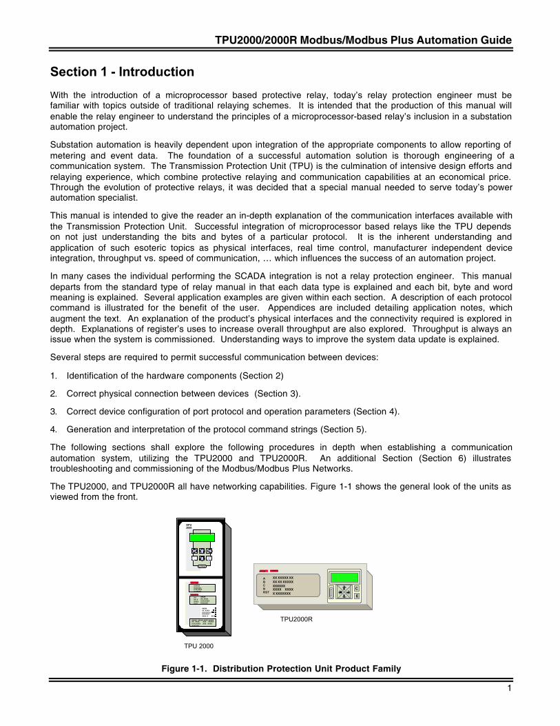
The TPU2000, and TPU2000R all have networking capabilities. Figure 1-1 shows the general look of the units asviewed from the front.
CC EE
STATUS
TARGETS
XXXXXXX XXXXX XX XXXXX XXXXX
XXXXXXX XXXXX XX XXXXX XXXXX
X XXX XX XX XX X X
XXXXXXX XXXXX XX XXXXX XXXXXXXXX X
XXXXX XXXXX XXXX XXXXXXX XXXX XXX XXXXXX XX XXXX XXX XXXXX XXXXX
DPU2000
E
C
ABCNRST
XX XXXXX XXXX XX XXXXXXXXXXX XXXX XXXXX XXXXXXX
STATUS TARGETS
TPU 2000
TPU2000R
Figure 1-1. Distribution Protection Unit Product Family
TPU2000/2000R Modbus/Modbus Plus Automation Guide
2
The products differentiate themselves as listed in Table 1-1. Table 1-1 lists the available protocols within therelays. Standard Ten Byte is an ABB protocol which is within the TPU2000 and TPU2000R protective relays.Standard Ten Byte is an asynchronous byte oriented protocol. The programming software (ECP [DOS ExternalCommunication Program] and WINECP [Windows External Communication Program]) allows configuration of therelay through a port on the units. Standard Ten Byte is available through an RS232 or RS485 port on the TPU.
INCOM is an ABB protocol, which is a derivative of Standard Ten Byte. It is a modulated synchronous bit streamusing the same commands as in the Standard Ten Byte protocol. INCOM is available as an option for theTPU2000 and TPU2000R relays as indicated within Table 1-1. Its physical interface is proprietary in that the TPUnode expects a modulated signal.
Modbus is an industrial de-facto standard protocol, which has been widely embraced by the utility industry.Modbus has two emulation’s, RTU, which is a synchronous protocol and ASCII which is an asynchronousprotocol. Modbus uses only one command set, but two emulation’s. Modbus strengths are that it uses astandard RS232 or RS485 interface to interconnect nodes on a network.
Modbus Plus is a hybrid protocol refinement of Modbus. Modbus Plus has a proprietary physical interface whichis available to device manufacturers through a connectivity program with Groupe Schneider. The interface offersgreater speed and communication features than Modbus.
DNP 3.0 is a protocol, which has its roots deep in the utility industry. It is an asynchronous protocol that allowsconnectivity through a standard RS232 or RS485 port. It includes such defined capabilities as file transfer, andtimestamping as part of the protocol, which makes it desirable for a utility implementation.
Table 1-1. Protocol Capabilities Listed by Product Type
PRODUCT PROTOCOL NOTESTPU2000 Standard Ten Byte Addressable Front Com, Com 1 and Aux Com
INCOM 2 Wire (and Shield) Current Injection Physical InterfaceModbus RS232 or RS485
DNP 3.0 RS232 or RS485TPU2000R Standard Ten Byte RS232 or RS485
INCOM 2 Wire (and Shield) Current Injection Physical InterfaceModbus RS232 or RS485Modbus Plus Proprietary Current Injection Physical InterfaceDNP 3.0 RS232 or RS485
Within this document, only Modbus, and Modbus Plus protocols shall be covered in depth. Standard 10 Byte,INCOM and DNP 3.0 shall be explained superficially. If one would need to reference the specific details ofStandard Ten Byte or INCOM protocols, please reference the engineering specifications concerning these topicsin Appendix A of this document.
TPU2000/2000R Modbus/Modbus Plus Automation Guide
3
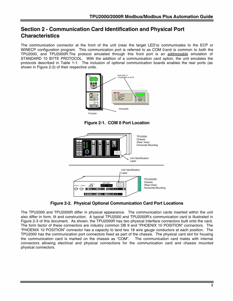
Section 2 - Communication Card Identification and Physical PortCharacteristics
The communication connector at the front of the unit (near the target LED’s) communicates to the ECP orWINECP configuration program. This communication port is referred to as COM 0 and is common to both theTPU2000, and TPU2000R.The protocol emulated through this front port is an addressable emulation ofSTANDARD 10 BYTE PROTOCOL. With the addition of a communication card option, the unit emulates theprotocols described in Table 1-1. The inclusion of optional communication boards enables the rear ports (asshown in Figure 2-2) of their respective units.
CC EE
STATUS
TARGETS
XXXXXXX XXXXX XX XXXX
X XXXXX
XXXXXXX XXXXX XX XXXXX XXXXX
X XXX XX X X XX XX
XXXXXXX XXXXX XX XXXX
X XXXXXXXXX X
XXXXX XXXXX XXXX XXXXXXX XXXX XXX XXXXXX XX XXXX XXX XXXXX XXXXX
DPU2000
E
C
ABCNRST
XX XXXXX XXXX XX XXXXXXXXXXX XXXX XXXXX XXXXXXX
STATUS TARGETS
TPU2000
TPU2000R
COM PORT 0- STANDARD 10 BYTE
Figure 2-1. COM 0 Port Location
Com 3Com 1 Com 2
AUX COM
TPU2000R/Chassis(Rear View)Horizontal Mounting
RS 232C
TPU2000Chassis(Rear View)Horizontal Mounting
AU
X C
OM
Model xxxxct xx p t xx
Model xxxxct xx pt xx
Unit Identification Label
Unit Identification Label
Figure 2-2. Physical Optional Communication Card Port Locations
The TPU2000 and TPU2000R differ in physical appearance. The communication cards inserted within the unitalso differ in form, fit and construction. A typical TPU2000 and TPU2000R’s communication card is illustrated inFigure 2-3 of this document. As shown, the TPU2000R has two physical interface connectors built onto the card.The form factor of these connectors are industry common DB 9 and “PHOENIX 10 POSITION” connectors. The“PHOENIX 10 POSITION” connector has a capacity to land two 18 wire gauge conductors at each position. TheTPU2000 has the communication port connectors fixed as part of the chassis. The physical card slot for housingthe communication card is marked on the chassis as “COM”. The communication card mates with internalconnectors allowing electrical and physical connections for the communication card and chassis mountedphysical connectors.
TPU2000/2000R Modbus/Modbus Plus Automation Guide
4
AUX/COM3.0
AUX/COM3.0
12345
TPU2000R COMMUNICATION CARD (TYPICAL)
TPU2000 COMMUNICATION CARD (TYPICAL)
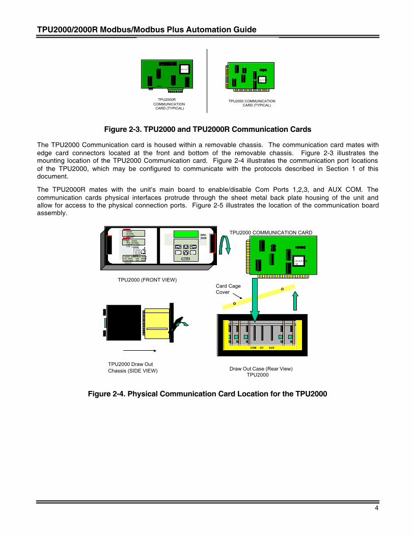
Figure 2-3. TPU2000 and TPU2000R Communication Cards
The TPU2000 Communication card is housed within a removable chassis. The communication card mates withedge card connectors located at the front and bottom of the removable chassis. Figure 2-3 illustrates themounting location of the TPU2000 Communication card. Figure 2-4 illustrates the communication port locationsof the TPU2000, which may be configured to communicate with the protocols described in Section 1 of thisdocument.
The TPU2000R mates with the unit’s main board to enable/disable Com Ports 1,2,3, and AUX COM. Thecommunication cards physical interfaces protrude through the sheet metal back plate housing of the unit andallow for access to the physical connection ports. Figure 2-5 illustrates the location of the communication boardassembly.
AUX/COM3.0
STATUS
TARGETS
XXXXXXX XXXXX XX XXXXX XXXXX
XXXXXXX XXXXX XX XXXXX XXXXX
XXXX XX XX XX XX
XXXXXXX XXXXX XX XXXXX XXXXXXXXX XXXXXX XXXXX XXXX XXXXX
XX XXXX XXX XXXXXX XX XXXX XXX XXXXX XXXXX
DPU2000
CC EE
TPU2000 Draw OutChassis (SIDE VIEW) Draw Out Case (Rear View)
TPU2000
COM I/O AUX
TPU2000 COMMUNICATION CARD
Card CageCover
TPU2000 (FRONT VIEW)
Figure 2-4. Physical Communication Card Location for the TPU2000
TPU2000/2000R Modbus/Modbus Plus Automation Guide
5
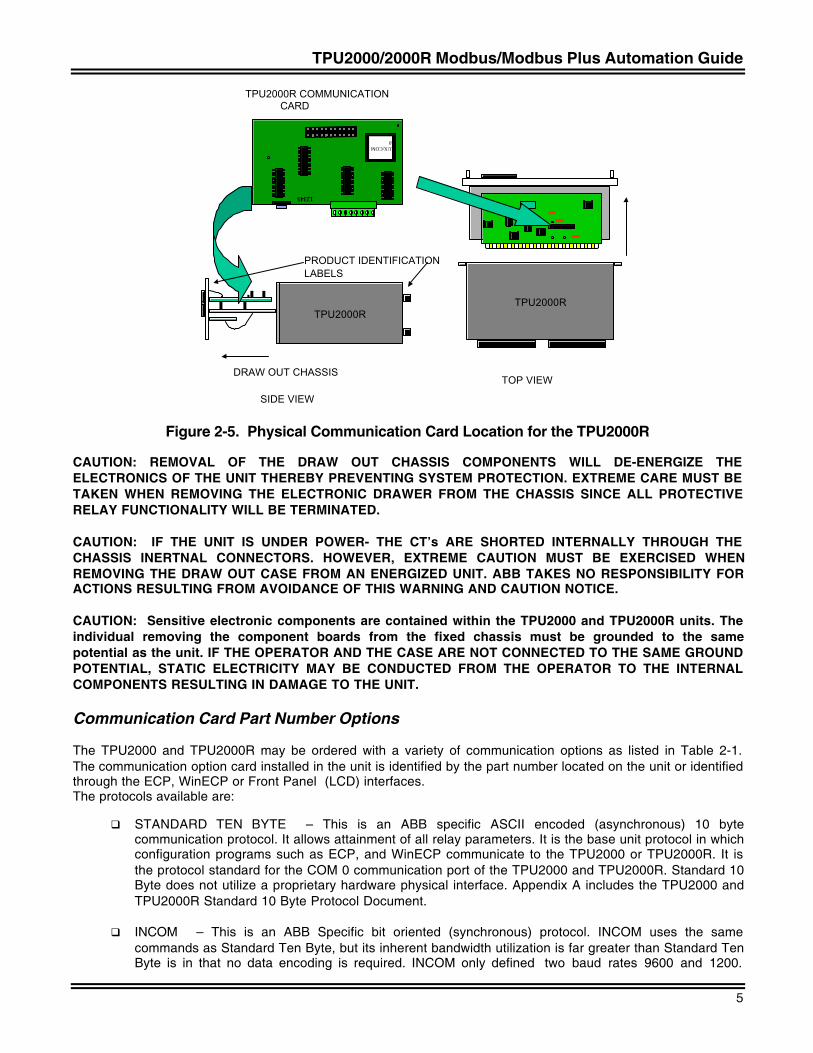
TPU2000R COMMUNICATION CARD
TPU2000R
DRAW OUT CHASSIS
PRODUCT IDENTIFICATIONLABELS
AUX/COM3.0
12345
SIDE VIEW
TPU2000R
TOP VIEW
Figure 2-5. Physical Communication Card Location for the TPU2000R
CAUTION: REMOVAL OF THE DRAW OUT CHASSIS COMPONENTS WILL DE-ENERGIZE THEELECTRONICS OF THE UNIT THEREBY PREVENTING SYSTEM PROTECTION. EXTREME CARE MUST BETAKEN WHEN REMOVING THE ELECTRONIC DRAWER FROM THE CHASSIS SINCE ALL PROTECTIVERELAY FUNCTIONALITY WILL BE TERMINATED.
CAUTION: IF THE UNIT IS UNDER POWER- THE CT’s ARE SHORTED INTERNALLY THROUGH THECHASSIS INERTNAL CONNECTORS. HOWEVER, EXTREME CAUTION MUST BE EXERCISED WHENREMOVING THE DRAW OUT CASE FROM AN ENERGIZED UNIT. ABB TAKES NO RESPONSIBILITY FORACTIONS RESULTING FROM AVOIDANCE OF THIS WARNING AND CAUTION NOTICE.
CAUTION: Sensitive electronic components are contained within the TPU2000 and TPU2000R units. Theindividual removing the component boards from the fixed chassis must be grounded to the samepotential as the unit. IF THE OPERATOR AND THE CASE ARE NOT CONNECTED TO THE SAME GROUNDPOTENTIAL, STATIC ELECTRICITY MAY BE CONDUCTED FROM THE OPERATOR TO THE INTERNALCOMPONENTS RESULTING IN DAMAGE TO THE UNIT.
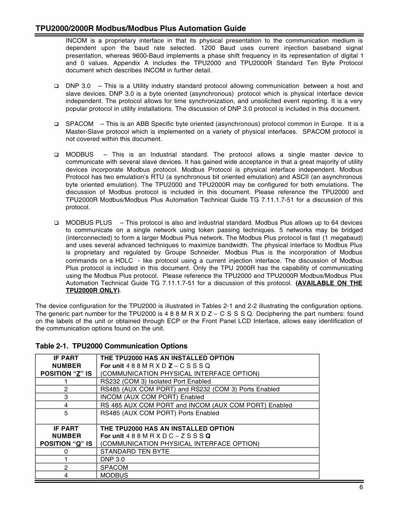
Communication Card Part Number Options
The TPU2000 and TPU2000R may be ordered with a variety of communication options as listed in Table 2-1.The communication option card installed in the unit is identified by the part number located on the unit or identifiedthrough the ECP, WinECP or Front Panel (LCD) interfaces.The protocols available are:
q STANDARD TEN BYTE – This is an ABB specific ASCII encoded (asynchronous) 10 bytecommunication protocol. It allows attainment of all relay parameters. It is the base unit protocol in whichconfiguration programs such as ECP, and WinECP communicate to the TPU2000 or TPU2000R. It isthe protocol standard for the COM 0 communication port of the TPU2000 and TPU2000R. Standard 10Byte does not utilize a proprietary hardware physical interface. Appendix A includes the TPU2000 andTPU2000R Standard 10 Byte Protocol Document.
q INCOM – This is an ABB Specific bit oriented (synchronous) protocol. INCOM uses the samecommands as Standard Ten Byte, but its inherent bandwidth utilization is far greater than Standard TenByte is in that no data encoding is required. INCOM only defined two baud rates 9600 and 1200.
TPU2000/2000R Modbus/Modbus Plus Automation Guide
6
INCOM is a proprietary interface in that its physical presentation to the communication medium isdependent upon the baud rate selected. 1200 Baud uses current injection baseband signalpresentation, whereas 9600-Baud implements a phase shift frequency in its representation of digital 1and 0 values. Appendix A includes the TPU2000 and TPU2000R Standard Ten Byte Protocoldocument which describes INCOM in further detail.
q DNP 3.0 – This is a Utility industry standard protocol allowing communication between a host andslave devices. DNP 3.0 is a byte oriented (asynchronous) protocol which is physical interface deviceindependent. The protocol allows for time synchronization, and unsolicited event reporting. It is a verypopular protocol in utility installations. The discussion of DNP 3.0 protocol is included in this document.
q SPACOM – This is an ABB Specific byte oriented (asynchronous) protocol common in Europe. It is aMaster-Slave protocol which is implemented on a variety of physical interfaces. SPACOM protocol isnot covered within this document.
q MODBUS – This is an Industrial standard. The protocol allows a single master device tocommunicate with several slave devices. It has gained wide acceptance in that a great majority of utilitydevices incorporate Modbus protocol. Modbus Protocol is physical interface independent. ModbusProtocol has two emulation’s RTU (a synchronous bit oriented emulation) and ASCII (an asynchronousbyte oriented emulation). The TPU2000 and TPU2000R may be configured for both emulations. Thediscussion of Modbus protocol is included in this document. Please reference the TPU2000 andTPU2000R Modbus/Modbus Plus Automation Technical Guide TG 7.11.1.7-51 for a discussion of thisprotocol.
q MODBUS PLUS – This protocol is also and industrial standard. Modbus Plus allows up to 64 devicesto communicate on a single network using token passing techniques. 5 networks may be bridged(interconnected) to form a larger Modbus Plus network. The Modbus Plus protocol is fast (1 megabaud)and uses several advanced techniques to maximize bandwidth. The physical interface to Modbus Plusis proprietary and regulated by Groupe Schneider. Modbus Plus is the incorporation of Modbuscommands on a HDLC- like protocol using a current injection interface. The discussion of ModbusPlus protocol is included in this document. Only the TPU 2000R has the capability of communicatingusing the Modbus Plus protocol. Please reference the TPU2000 and TPU2000R Modbus/Modbus PlusAutomation Technical Guide TG 7.11.1.7-51 for a discussion of this protocol. (AVAILABLE ON THETPU2000R ONLY).
The device configuration for the TPU2000 is illustrated in Tables 2-1 and 2-2 illustrating the configuration options.The generic part number for the TPU2000 is 4 8 8 M R X D Z – C S S S Q. Deciphering the part numbers: foundon the labels of the unit or obtained through ECP or the Front Panel LCD Interface, allows easy identification ofthe communication options found on the unit.
Table 2-1. TPU2000 Communication Options
IF PARTNUMBER
POSITION “Z” IS
THE TPU2000 HAS AN INSTALLED OPTIONFor unit 4 8 8 M R X D Z – C S S S Q(COMMUNICATION PHYSICAL INTERFACE OPTION)
1 RS232 (COM 3) Isolated Port Enabled2 RS485 (AUX COM PORT) and RS232 (COM 3) Ports Enabled3 INCOM (AUX COM PORT) Enabled4 RS 485 AUX COM PORT and INCOM (AUX COM PORT) Enabled5 RS485 (AUX COM PORT) Ports Enabled
IF PARTNUMBER
POSITION “Q” IS
THE TPU2000 HAS AN INSTALLED OPTIONFor unit 4 8 8 M R X D C – Z S S S Q(COMMUNICATION PHYSICAL INTERFACE OPTION)
0 STANDARD TEN BYTE1 DNP 3.02 SPACOM4 MODBUS
TPU2000/2000R Modbus/Modbus Plus Automation Guide
7
Table 2-2. TPU2000 Communication Card Matrix for Unit 4 8 8 M R X D Z – C S S S Q
“Z” Digit “Q” Digit COM 3 AUX COM RS485 INCOM IRIG B1 0 Standard 10 Byte RS2322 0 Standard 10 Byte RS232 Standard 10 Byte Available2 1 Standard 10 Byte or
DNP 3.0 RS232Standard 10 Byteor DNP 3.0
2 2 Standard 10 Byte RS232 SPACOM2 4 Standard 10 Byte or
Modbus RS232Standard 10 Byteor Modbus
Available
3 0 Available Available4 0 Standard 10 Byte Available Available4 1 DNP 3.0 Available Available4 2 SPACOM4 4 Modbus Available Available5 0 Standard 10 Byte
The device configuration for the TPU2000R is illustrated in Tables 2-3 and 2-4 illustrating the configurationoptions. The generic part number for the TPU2000 is 5 8 8 X X X Y Z – X X X X Q. Deciphering the part numbers:found on the labels of the unit or obtained through ECP or the Front Panel LCD Interface, allows easyidentification of the communication options found on the unit.
Table 2-3. TPU2000R Communication Options
IF PARTNUMBER
POSITION “Y” IS
THE TPU2000R HAS AN INSTALLED OPTIONFor unit 5 8 8 X X X Y Z – X X X X Q (X = Don’t Care)(FRONT PANEL INTERFACE OPTION)
0 Horizontal Unit Mounting – No front panel LCD interface.1 Horizontal Unit Mounting – Front panel LCD interface is included.5 Vertical Unit Mounting – No front panel LCD interface.6 Vertical Unit Mounting – Front panel LCD interface is included.
IF PARTNUMBER
POSITION “Z” IS
THE TPU2000R HAS AN INSTALLED OPTIONFor unit 5 8 8 X X X Y Z – X X X X Q ( X = Don’t Care)(COMMUNICATION PHYSICAL INTERFACE OPTION)
0 RS232 (COM 1) Non-Isolated Port is active on the unit.1 RS232 (COM 2) Isolated Port Only is active on the unit. (SEE NOTE)2 RS485 (AUX COM PORT) and RS232 (COM 3) Ports on Option Card.3 INCOM (AUX COM PORT) and RS485 (AUX COM PORT) Ports on Option Card.4 INCOM (AUX COM PORT) and RS485 (AUX COM PORT) Ports on Option Card.5 RS485 (AUX COM PORT) Port On Option Card.6 Modbus Plus Port (COM 3) on the Option Card.7 Modbus Plus (COM 3) and RS485 (AUX COM PORT) on the Option Card.8 RS485 (COM 3) and RS485 (AUX COM PORT) Ports on the Option Card.
NOTE: * = If the option denoted in part number position “Y” is a 0 or 5, the COM 2port is enabled, if the option denoted in part number position “Y” is a 2 or 6 theCOM 2 Port is disabled.
IF PARTNUMBER
POSITION “Q” IS
THE TPU2000R HAS AN INSTALLED OPTIONFor unit 5 8 8 X X X Y Z – X X X X Q (X = Don’t Care)(COMMUNICATION PHYSICAL INTERFACE OPTION)
0 STANDARD TEN BYTE1 DNP 3.04 Modbus/Modbus Plus (Depending on hardware interface selected in Position Z)
TPU2000/2000R Modbus/Modbus Plus Automation Guide
8
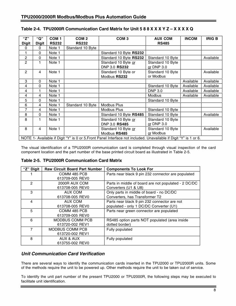
Table 2-4. TPU2000R Communication Card Matrix for Unit 5 8 8 X X X Y Z – X X X X Q
“Z”Digit
“Q”Digit
COM 1RS232
COM 2RS232
COM 3 AUX COMRS485
INCOM IRIG B
0 0 Note 1 Standard 10 Byte1 0 Note 1 Standard 10 Byte RS2322 0 Note 1 Standard 10 Byte RS232 Standard 10 Byte Available2 1 Note 1 Standard 10 Byte or
DNP 3.0 RS232Standard 10 Byteor DNP 3.0
2 4 Note 1 Standard 10 Byte orModbus RS232
Standard 10 Byteor Modbus
Available
3 0 Note 1 Available Available4 0 Note 1 Standard 10 Byte Available Available4 1 Note 1 DNP 3.0 Available Available4 4 Note 1 Modbus Available Available5 0 Note 1 Standard 10 Byte6 4 Note 1 Standard 10 Byte Modbus Plus7 4 Note 1 Modbus Plus Standard 10 Byte8 0 Note 1 Standard 10 Byte RS485 Standard 10 Byte Available8 1 Note 1 Standard 10 Byte or
DNP 3.0 RS485Standard 10 Byteor DNP 3.0
8 4 Note 1 Standard 10 Byte orModbus RS485
Standard 10 Byteor Modbus
Available
NOTE 1- Available if Digit “Y” is 0 or 5.Front Panel Interface not included. Unavailable if Digit “Y” is 1 or 6.
The visual identification of a TPU2000R communication card is completed through visual inspection of the cardcomponent location and the part number of the base printed circuit board as illustrated in Table 2-5.
Table 2-5. TPU2000R Communication Card Matrix
“Z” Digit Raw Circuit Board Part Number Components To Look For1 COMM 485 PCB
613709-005 REV0Parts near black 9 pin 232 connector are populated
2 2000R AUX COM613708-005 REV0
Parts in middle of board are not populated - 2 DC/DCConverters (U1 & U8)
3 AUX COM613708-005 REV0
Only parts in middle of board - no DC/DCConverters, has Transformer T2
4 AUX COM613708-005 REV0
Parts near black 9 pin 232 connector are notpopulated - only 1 DC/DC Converter (U1)
5 COMM 485 PCB613709-005 REV0
Parts near green connector are populated
6 MODBUS COMM PCB613720-002 REV1
RS485 option parts NOT populated (area insidedotted border)
7 MODBUS COMM PCB613720-002 REV1
Fully populated
8 AUX & AUX613755-002 REV0
Fully populated
Unit Communication Card Verification
There are several ways to identify the communication cards inserted in the TPU2000 or TPU2000R units. Someof the methods require the unit to be powered up. Other methods require the unit to be taken out of service.
To identify the unit part number of the present TPU2000 or TPU2000R, the following steps may be executed tofacilitate unit identification.
TPU2000/2000R Modbus/Modbus Plus Automation Guide
9
1. With the unit energized, if the unit has a Front Panel LCD (Refer to Tables 2-1 through 2-4 inclusive foridentification) Interface:
1. Depress the “E” Key.2. Depress the Arrow Down Key “↓” once to highlight the SETTINGS field. Depress the “E”
Key.3. Depress the Arrow Down Key “↓” twice to highlight the UNIT INFORMATION field.
Depress the “E” key.4. The Serial Number and Catalog Number shall be displayed.
If the Unit does not have a Front Panel LCD Interface (Refer to Tables 2-1 through 2-4 inclusive for identification)and the user has DOS ECP or if the user wishes not to use the unit’s Front Panel LCD Interface:
1. Start ECP.2. Select the appropriate communication parameters so that the personal computer
attached to the TPU2000 or TPU2000R will communicate via the null modem cableconnection. (See Figure 3-3 or Figure 3-4)
3. Depress enter to allow attachment of the unit.4. The Serial Number and Catalog Number shall be displayed.
If the Unit does not have a Front Panel LCD Interface (Refer to Tables 2-1 through 2-4 inclusive for identification)and the user has WinECP or if the user wishes not to use the unit’s Front Panel Interface:
1. Start WinECP.2. Depress the “DIRECT ACCESS” selection button presented in the pop-up window.3. Depress the “CONNECT” option selection presented within the pop-up window.4. Select the “HELP” Menu option at the top right-hand section of the menu bar.5. Select the Drag-Down Menu item “UNIT INFORMATION”.6. A pop-up window shall appear with the Serial Number and Catalog Number.
2. At the back of the TPU2000 or the TPU2000R chassis, in the left-hand lower section of the unit, a label shallappear indicating the serial number and model number of the unit. It should match the data presented in theECP, WinECP or Front Panel Interface (FPI) Menus. If it does not, please contact the factory.
3. As a final check, if the TPU2000 or TPU2000R can be powered-down or if protection can be interrupted,loosen the front panel screws at the front of the unit. Remove the product component drawer from thechassis. Face the front panel interface, and rotate the board so that the semiconductor components aredirectly visible. On the backside of the metal panel supporting the Front Panel Interface, a label shall beavailable indicating the serial number and model number. These numbers should match those obtained insteps 1 and 2. If they do not, please contact the factory.
TPU2000/2000R Modbus/Modbus Plus Automation Guide
10
Section 3 - TPU2000 and TPU2000R Device Connectivity
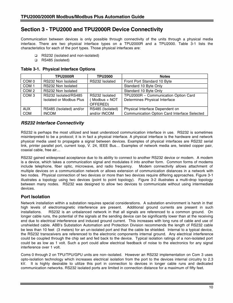
Communication between devices is only possible through connectivity of the units through a physical mediainterface. There are two physical interface types on a TPU2000R and a TPU2000. Table 3-1 lists thecharacteristics for each of the port types. Those physical interfaces are:
q RS232 (isolated and non-isolated)q RS485 (isolated)
Table 3-1. Physical Interface Options
TPU2000R TPU2000 NotesCOM 0 RS232 Non Isolated RS232 Isolated Front Port Standard 10 ByteCOM 1 RS232 Non Isolated Standard 10 Byte OnlyCOM 2 RS232 Non Isolated Standard 10 Byte OnlyCOM 3 RS232 Isolated/RS485
Isolated or Modbus PlusRS232 Isolated( Modbus + NOTOFFERED)
TPU2000R – Communication Option CardDetermines Physical Interface
AUXCOM
RS485 (Isolated) and/orINCOM
RS485 (Isolated)and/or INCOM
Physical Interface Dependent onCommunication Option Card Interface Selected
RS232 Interface Connectivity
RS232 is perhaps the most utilized and least understood communication interface in use. RS232 is sometimesmisinterpreted to be a protocol; it is in fact a physical interface. A physical interface is the hardware and networkphysical media used to propagate a signal between devices. Examples of physical interfaces are RS232 seriallink, printer parallel port, current loop, V. 24, IEEE Bus… Examples of network media are, twisted copper pair,coaxial cable, free air…
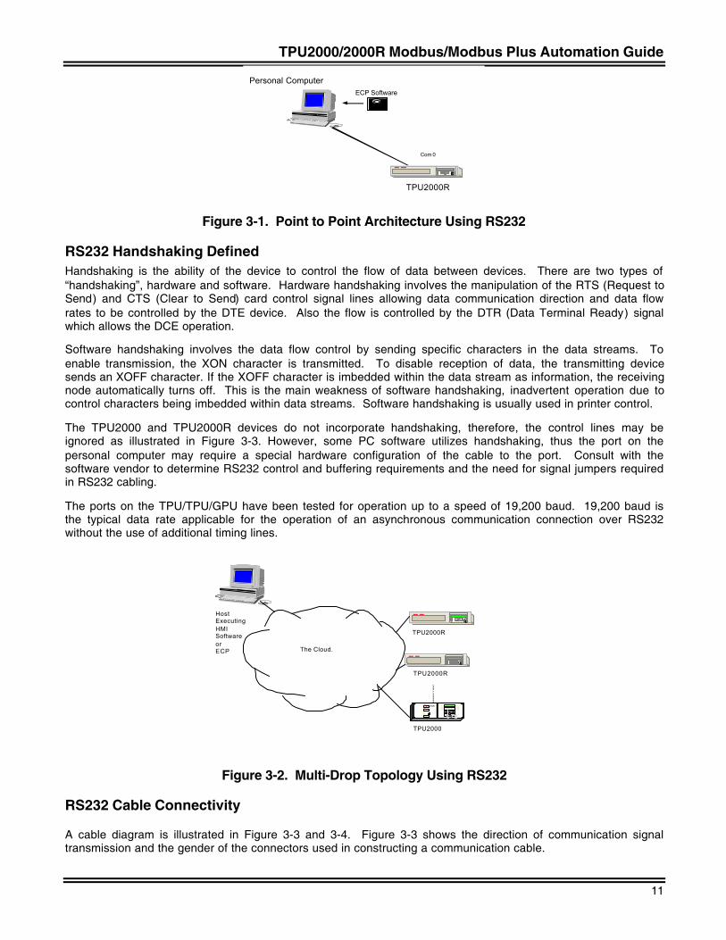
RS232 gained widespread acceptance due to its ability to connect to another RS232 device or modem. A modemis a device, which takes a communication signal and modulates it into another form. Common forms of modemsinclude telephone, fiber optic, microwave, and radio frequency. Modem connectivity allows attachment ofmultiple devices on a communication network or allows extension of communication distances in a network withtwo nodes. Physical connection of two devices or more than two devices require differing approaches. Figure 3-1illustrates a topology using two devices (point to point topology). Figure 3-2 illustrates a multi-drop topologybetween many nodes. RS232 was designed to allow two devices to communicate without using intermediatedevices.
Port IsolationNetwork installation within a substation requires special considerations. A substation environment is harsh in thathigh levels of electromagnetic interference are present. Additional ground currents are present in suchinstallations. RS232 is an unbalanced network in that all signals are referenced to a common ground. Onlonger cable runs, the potential of the signals at the sending device can be significantly lower than at the receivingend due to electrical interference and induced ground current. This increases with long runs of cable and use ofunshielded cable. ABB’s Substation Automation and Protection Division recommends the length of RS232 cablebe less than 10 feet (3 meters) for an un-isolated port and that the cable be shielded. Internal to a typical device,the RS232 transceivers are referenced to the electronic components internal ground. Any electrical interferencecould be coupled through the chip set and fed back to the device. Typical isolation ratings of a non-isolated portcould be as low as 1 volt. Such a port could allow electrical feedback of noise to the electronics for any signalinterference over 1 volt.
Coms 0 through 2 on TPU/TPU/GPU units are non–isolated. However an RS232 implementation on Com 3 usesopto-isolation technology which increases electrical isolation from the port to the devices internal circuitry to 2.3kV. It is highly desirable to utilize this port in connection to devices in longer cable runs and dedicatedcommunication networks. RS232 isolated ports are limited in connection distance for a maximum of fifty feet.
TPU2000/2000R Modbus/Modbus Plus Automation Guide
11
EC
TPU2000R
Personal ComputerECP Software
Com 0
Figure 3-1. Point to Point Architecture Using RS232
RS232 Handshaking DefinedHandshaking is the ability of the device to control the flow of data between devices. There are two types of“handshaking”, hardware and software. Hardware handshaking involves the manipulation of the RTS (Request toSend) and CTS (Clear to Send) card control signal lines allowing data communication direction and data flowrates to be controlled by the DTE device. Also the flow is controlled by the DTR (Data Terminal Ready) signalwhich allows the DCE operation.
Software handshaking involves the data flow control by sending specific characters in the data streams. Toenable transmission, the XON character is transmitted. To disable reception of data, the transmitting devicesends an XOFF character. If the XOFF character is imbedded within the data stream as information, the receivingnode automatically turns off. This is the main weakness of software handshaking, inadvertent operation due tocontrol characters being imbedded within data streams. Software handshaking is usually used in printer control.
The TPU2000 and TPU2000R devices do not incorporate handshaking, therefore, the control lines may beignored as illustrated in Figure 3-3. However, some PC software utilizes handshaking, thus the port on thepersonal computer may require a special hardware configuration of the cable to the port. Consult with thesoftware vendor to determine RS232 control and buffering requirements and the need for signal jumpers requiredin RS232 cabling.
The ports on the TPU/TPU/GPU have been tested for operation up to a speed of 19,200 baud. 19,200 baud isthe typical data rate applicable for the operation of an asynchronous communication connection over RS232without the use of additional timing lines.
Figure 3-2. Multi-Drop Topology Using RS232
RS232 Cable Connectivity
A cable diagram is illustrated in Figure 3-3 and 3-4. Figure 3-3 shows the direction of communication signaltransmission and the gender of the connectors used in constructing a communication cable.
Host ExecutingHMI Softwareor ECP
TPU2000
EC
EC
TPU2000R
The Cloud.
TPU2000R
STATUS
CC EE
TPU2000/2000R Modbus/Modbus Plus Automation Guide
12
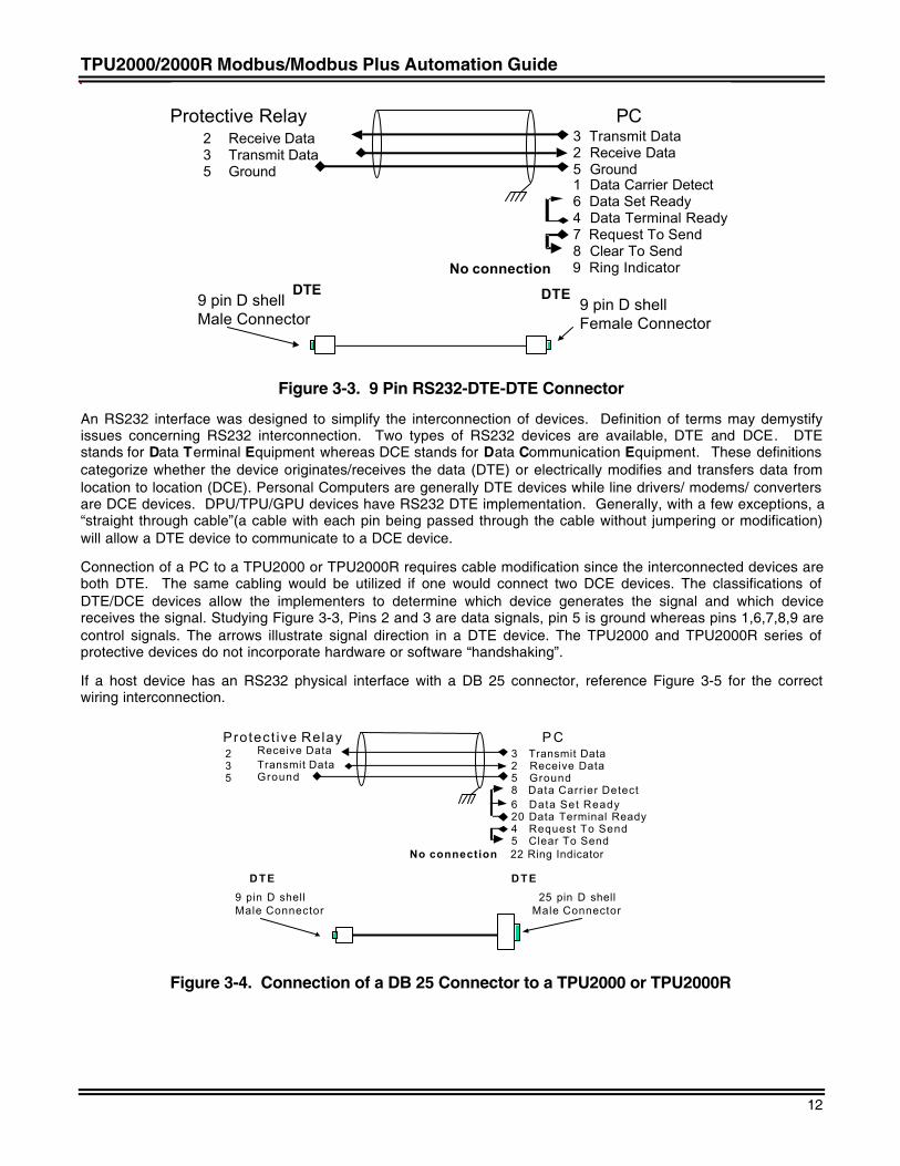
Protective Relay PC2 Receive Data 3 Transmit Data3 Transmit Data 2 Receive Data5 Ground 5 Ground
1 Data Carrier Detect6 Data Set Ready
4 Data Terminal Ready7 Request To Send8 Clear To Send
No connection 9 Ring Indicator
9 pin D shellMale Connector
9 pin D shellFemale Connector
DTE DTE
Figure 3-3. 9 Pin RS232-DTE-DTE Connector
An RS232 interface was designed to simplify the interconnection of devices. Definition of terms may demystifyissues concerning RS232 interconnection. Two types of RS232 devices are available, DTE and DCE. DTEstands for Data Terminal Equipment whereas DCE stands for Data Communication Equipment. These definitionscategorize whether the device originates/receives the data (DTE) or electrically modifies and transfers data fromlocation to location (DCE). Personal Computers are generally DTE devices while line drivers/ modems/ convertersare DCE devices. DPU/TPU/GPU devices have RS232 DTE implementation. Generally, with a few exceptions, a“straight through cable”(a cable with each pin being passed through the cable without jumpering or modification)will allow a DTE device to communicate to a DCE device.
Connection of a PC to a TPU2000 or TPU2000R requires cable modification since the interconnected devices areboth DTE. The same cabling would be utilized if one would connect two DCE devices. The classifications ofDTE/DCE devices allow the implementers to determine which device generates the signal and which devicereceives the signal. Studying Figure 3-3, Pins 2 and 3 are data signals, pin 5 is ground whereas pins 1,6,7,8,9 arecontrol signals. The arrows illustrate signal direction in a DTE device. The TPU2000 and TPU2000R series ofprotective devices do not incorporate hardware or software “handshaking”.
If a host device has an RS232 physical interface with a DB 25 connector, reference Figure 3-5 for the correctwiring interconnection.
Protect ive Relay P C2 Receive Data 3 Transmit Data3 Transmit Data 2 Receive Data5 Ground 5 Ground
8 Data Carrier Detect6 Data Set Ready
20 Data Terminal Ready4 Request To Send5 Clear To Send
No connection 22 Ring Indicator
9 pin D shellMale Connector
25 pin D shellMale Connector
D T E D T E
Figure 3-4. Connection of a DB 25 Connector to a TPU2000 or TPU2000R
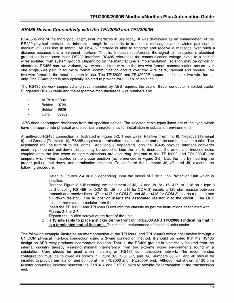
TPU2000/2000R Modbus/Modbus Plus Automation Guide
13
RS485 Device Connectivity with the TPU2000 and TPU2000R
RS485 is one of the more popular physical interfaces in use today. It was developed as an enhancement of theRS422 physical interface. Its inherent strength is its ability to transmit a message over a twisted pair coppermedium of 3000 feet in length. An RS485 interface is able to transmit and receive a message over such adistance because it is a balanced interface. That is, it does not reference the signal to the system’s electricalground, as is the case in an RS232 interface. RS485 references the communication voltage levels to a pair ofwires isolated from system ground. Depending on the manufacturer’s implementation, isolation may be optical orelectronic. RS485 has two variants, two wires and four-wire. In the two-wire format, communication occurs overone single wire pair. In four-wire format, communication occurs over two wire pairs, transmit and receive. Thetwo-wire format is the most common in use. The TPU2000 and TPU2000R support half duplex two-wire formatonly. The RS485 port is also optically isolated to provide for 3000 V of isolation.
The RS485 network supported and recommended by ABB requires the use of three conductor shielded cable.Suggested RS485 cable and the respective manufacturer’s wire numbers are:
• ALPHA 58902• Belden 9729• Belden 9829• Carol 58902
ABB does not support deviations from the specified cables. The selected cable types listed are of the type whichhave the appropriate physical and electrical characteristics for installation in substation environments.
A multi-drop RS485 connection is illustrated in Figure 3-2. Three wires, Positive (Terminal 9), Negative (Terminal8) and Ground (Terminal 10). RS485 requires a termination resistor at each end of the communication cable. Theresistance shall be from 90 to 120 ohms. Additionally, depending upon the RS485 physical interface converterused, a pull-up and pull-down resistor may be added to bias the line to decrease the amount of induced noisecoupled onto the line when no communications are occurring. Internal to the TPU2000 and TPU2000R arejumpers which when inserted in the proper position (as referenced in Figure 3-5), bias the line by inserting theproper pull-up, pull-down, and termination resistors. To configure the Jumpers J6, J7, and J8, execute thefollowing procedure:
q Refer to Figures 2-4 or 2-5 depending upon the model of Distribution Protection Unit which isinstalled.
q Refer to Figure 3-6 illustrating the placement of J6, J7 and J8 (or J16, J17, or J 18 on a type 8card enabling RS 485 for COM 3). J6 (or J16 for COM 3) inserts a 120 ohm resistor betweentransmit and receive lines. J7 or (J17 for COM 3) and J8 or (J18 for COM 3) inserts a pull-up andpull-down resistor. The IN position inserts the associated resistor in to the circuit. The OUTposition removes the resistor from the circuit.
q Insert the TPU2000 and TPU2000R unit into the chassis as per the instructions associated withFigures 2-4 or 2-5.
q Tighten the knurled screws at the front of the unit.q IT IS advisable to place a sticker on the front of TPU2000 AND TPU2000R indicating that it
is a terminated end of line unit. This makes maintenance of installed units easier.
The following example illustrates an interconnection of the TPU2000 and TPU2000R with a host device through aUNICOM physical interface connection using a 3-wire connection method. It should be noted that the RS485design on ABB relay products incorporates isolation. That is, the RS485 ground is electrically isolated from theinternal circuitry thereby assuring minimal interference from the extreme noise environments found in asubstation. Care should be used when installing an RS485 communication network. The recommendedconfiguration must be followed as shown in Figure 3-5, 3-6, 3-7, and 3-8. Jumpers J6, J7, and J8 should beinserted to provide termination and pull-up at the TPU2000 and TPU2000R end. Although not shown, a 120 ohmresistor should be inserted between the TX/RX + and TX/RX- pairs to provide for termination at the transmissionend.
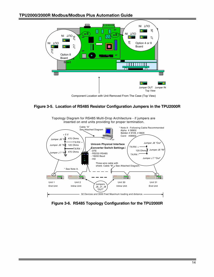
TPU2000/2000R Modbus/Modbus Plus Automation Guide
14
Jumper OUT Jumper IN Top View
Component Location with Unit Removed From The Case (Top View)
J8
J7
J6
OUT IN
OUT IN
Option 8Board
Option 4 or 8Board
J18
J17
J
16
OUT IN
OUT IN
Option 8Board
Figure 3-5. Location of RS485 Resistor Configuration Jumpers in the TPU2000R
Unicom Physical Interface Converter Switch Settings :- DTE- RS232-RS485- 19200 Baud- HD
Cable “A”See Attached Diagram
ECEC EC
32 Devices and 3000 Feet Maximum loading and distance.
EC
Unit 1 Unit 2 Unit 30 Unit 31
Three-wire cable withshield. Cable “B” - See Attached Diagram.
End Unit Inline Unit Inline Unit End UnitJumpersJ6, J7, J8 “OUT”
+ 5 V
120 Ohms
470 Ohms
470 Ohms
Jumper J8 “IN
Jumper J 7 “IN”
Jumper J6 “IN”TX/RX +
TX/RX -
Topology Diagram for RS485 Multi-Drop Architecture - if jumpers are inserted on end units providing for proper termination.
* See Note A.
* Note A - Following Cable Recommended Alpha # 58902 Belden # 9729, # 9829 Carol #58902
120 Ohms
Jumper J8 “Out”
Jumper J6 “IN”TX/RX +
TX/RX -
Jumper J 7 “Out”
Figure 3-6. RS485 Topology Configuration for the TPU2000R
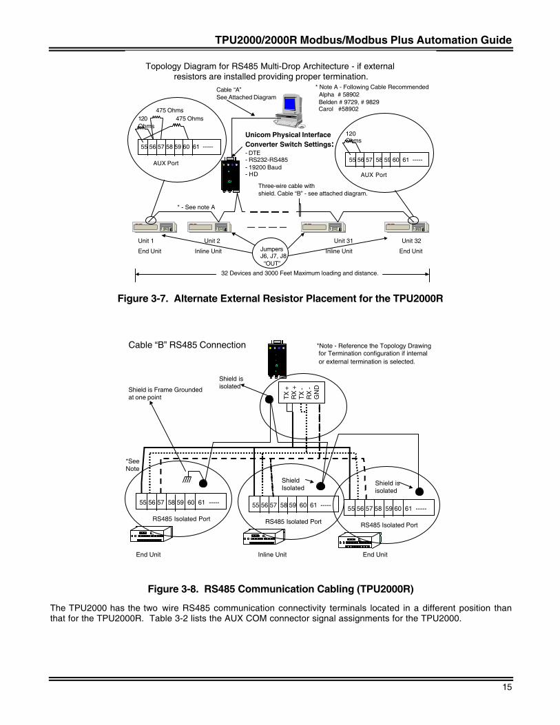
TPU2000/2000R Modbus/Modbus Plus Automation Guide
15
Unicom Physical Interface Converter Switch Settings:- DTE- RS232-RS485- 19200 Baud- HD
Cable “A”See Attached Diagram
ECEC EC
32 Devices and 3000 Feet Maximum loading and distance.
EC
Unit 1 Unit 2 Unit 31 Unit 32
Three-wire cable withshield. Cable “B” - see attached diagram.
End Unit Inline Unit Inline Unit End UnitJumpersJ6, J7, J8 “OUT”
Topology Diagram for RS485 Multi-Drop Architecture - if external resistors are installed providing proper termination.
55 56 57 58 59 60 61 -----
475 Ohms475 Ohms
120Ohms
AUX Port
* - See note A
* Note A - Following Cable Recommended Alpha # 58902 Belden # 9729, # 9829 Carol #58902
55 56 57 58 59 60 61 -----
120Ohms
AUX Port
Figure 3-7. Alternate External Resistor Placement for the TPU2000RTX
+R
X +
TX -
RX
-G
ND
3
55 56 57 58 59 60 61 -----
RS485 Isolated Port
Shield is isolatedShield is Frame Grounded
at one point
3
55 56 57 58 59 60 61 -----
RS485 Isolated Port
3
55 56 57 58 59 60 61 -----
RS485 Isolated Port
End Unit Inline Unit End Unit
Shield Isolated
Shield isisolated
Cable “B” RS485 Connection
*SeeNote
*Note - Reference the Topology Drawing for Termination configuration if internal or external termination is selected.
Figure 3-8. RS485 Communication Cabling (TPU2000R)
The TPU2000 has the two wire RS485 communication connectivity terminals located in a different position thanthat for the TPU2000R. Table 3-2 lists the AUX COM connector signal assignments for the TPU2000.
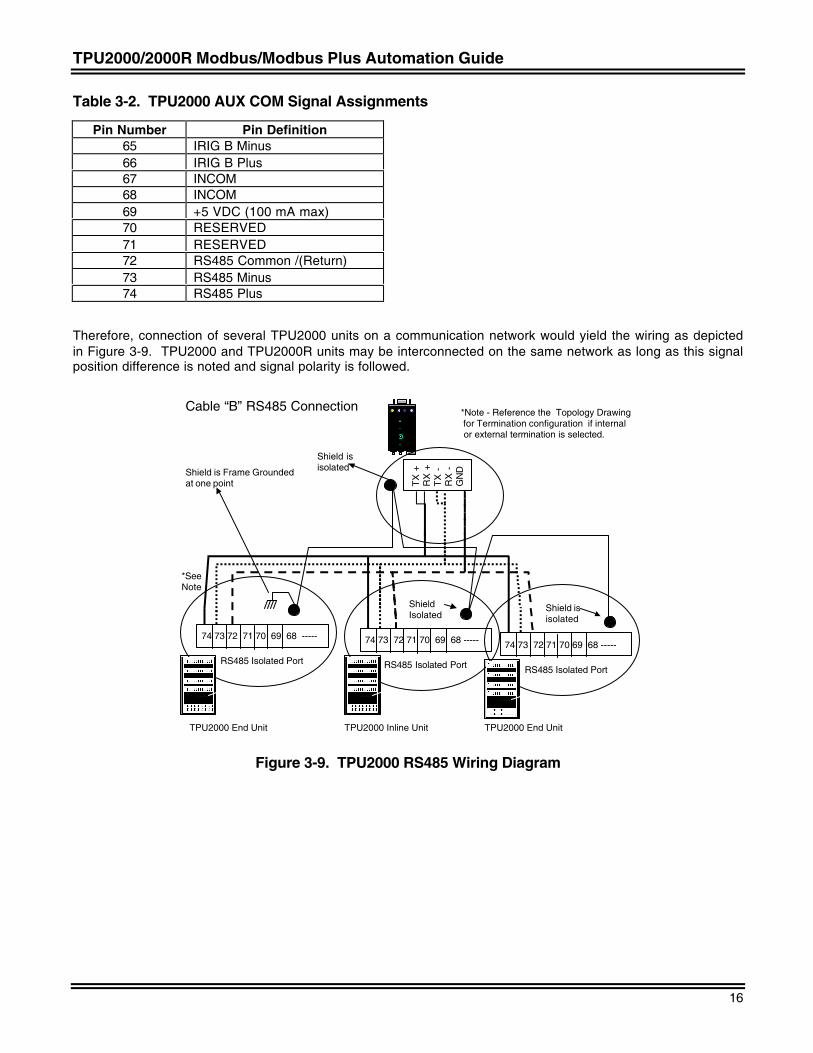
TPU2000/2000R Modbus/Modbus Plus Automation Guide
16
Table 3-2. TPU2000 AUX COM Signal Assignments
Pin Number Pin Definition65 IRIG B Minus66 IRIG B Plus67 INCOM68 INCOM69 +5 VDC (100 mA max)70 RESERVED71 RESERVED72 RS485 Common /(Return)73 RS485 Minus74 RS485 Plus
Therefore, connection of several TPU2000 units on a communication network would yield the wiring as depictedin Figure 3-9. TPU2000 and TPU2000R units may be interconnected on the same network as long as this signalposition difference is noted and signal polarity is followed.
TX
+R
X +
TX
-R
X -
GN
D
74 73 72 71 70 69 68 -----
RS485 Isolated Port
Shield is isolatedShield is Frame Grounded
at one point
74 73 72 71 70 69 68 -----
RS485 Isolated Port
74 73 72 71 70 69 68 -----
RS485 Isolated Port
TPU2000 End Unit TPU2000 Inline Unit TPU2000 End Unit
Shield Isolated
Shield isisolated
Cable “B” RS485 Connection
*SeeNote
*Note - Reference the Topology Drawing for Termination configuration if internal or external termination is selected.
Figure 3-9. TPU2000 RS485 Wiring Diagram
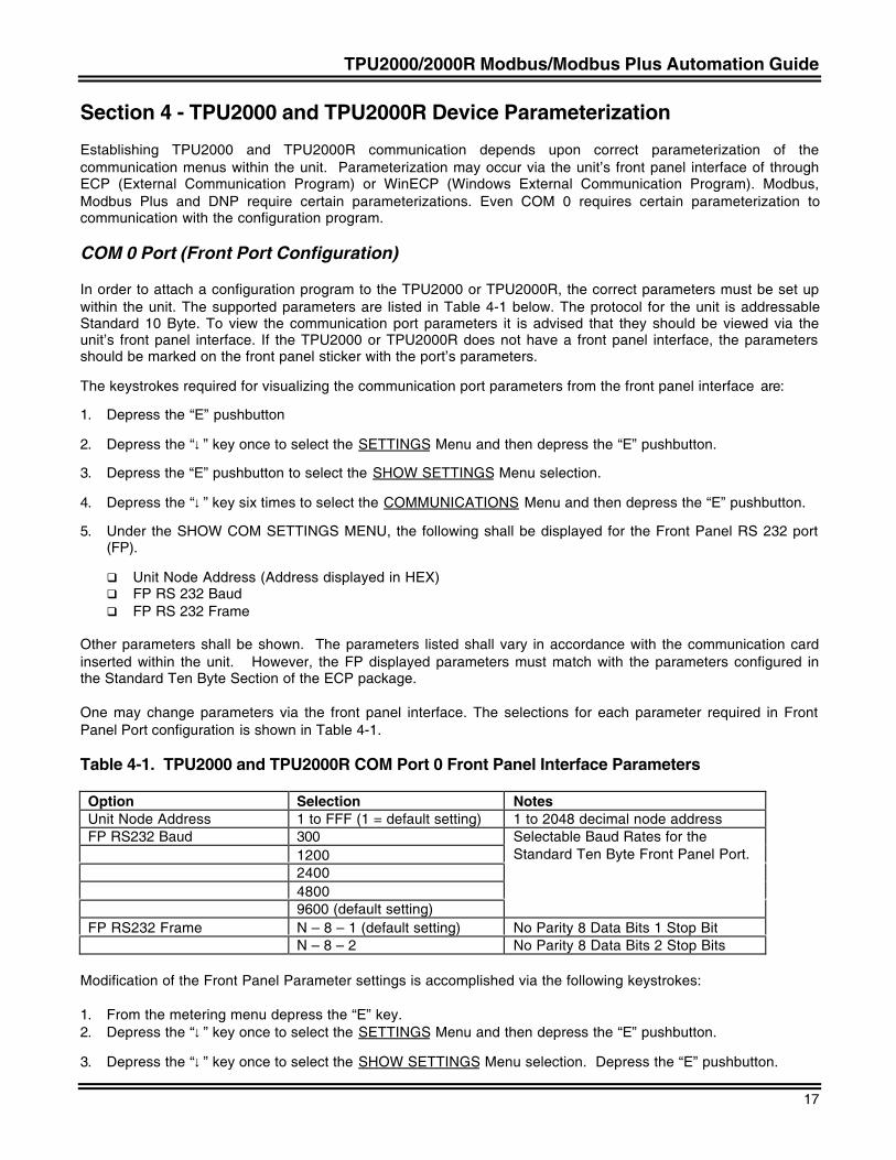
TPU2000/2000R Modbus/Modbus Plus Automation Guide
17
Section 4 - TPU2000 and TPU2000R Device Parameterization
Establishing TPU2000 and TPU2000R communication depends upon correct parameterization of thecommunication menus within the unit. Parameterization may occur via the unit’s front panel interface of throughECP (External Communication Program) or WinECP (Windows External Communication Program). Modbus,Modbus Plus and DNP require certain parameterizations. Even COM 0 requires certain parameterization tocommunication with the configuration program.
COM 0 Port (Front Port Configuration)
In order to attach a configuration program to the TPU2000 or TPU2000R, the correct parameters must be set upwithin the unit. The supported parameters are listed in Table 4-1 below. The protocol for the unit is addressableStandard 10 Byte. To view the communication port parameters it is advised that they should be viewed via theunit’s front panel interface. If the TPU2000 or TPU2000R does not have a front panel interface, the parametersshould be marked on the front panel sticker with the port’s parameters.
The keystrokes required for visualizing the communication port parameters from the front panel interface are:
1. Depress the “E” pushbutton
2. Depress the “↓” key once to select the SETTINGS Menu and then depress the “E” pushbutton.
3. Depress the “E” pushbutton to select the SHOW SETTINGS Menu selection.
4. Depress the “↓” key six times to select the COMMUNICATIONS Menu and then depress the “E” pushbutton.
5. Under the SHOW COM SETTINGS MENU, the following shall be displayed for the Front Panel RS 232 port(FP).
q Unit Node Address (Address displayed in HEX)q FP RS 232 Baudq FP RS 232 Frame
Other parameters shall be shown. The parameters listed shall vary in accordance with the communication cardinserted within the unit. However, the FP displayed parameters must match with the parameters configured inthe Standard Ten Byte Section of the ECP package.
One may change parameters via the front panel interface. The selections for each parameter required in FrontPanel Port configuration is shown in Table 4-1.
Table 4-1. TPU2000 and TPU2000R COM Port 0 Front Panel Interface Parameters
Option Selection NotesUnit Node Address 1 to FFF (1 = default setting) 1 to 2048 decimal node addressFP RS232 Baud 300
1200240048009600 (default setting)
Selectable Baud Rates for theStandard Ten Byte Front Panel Port.
FP RS232 Frame N – 8 – 1 (default setting) No Parity 8 Data Bits 1 Stop BitN – 8 – 2 No Parity 8 Data Bits 2 Stop Bits
Modification of the Front Panel Parameter settings is accomplished via the following keystrokes:
1. From the metering menu depress the “E” key.2. Depress the “↓” key once to select the SETTINGS Menu and then depress the “E” pushbutton.
3. Depress the “↓” key once to select the SHOW SETTINGS Menu selection. Depress the “E” pushbutton.
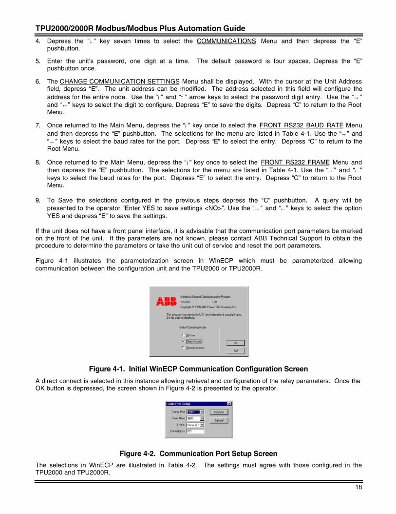
TPU2000/2000R Modbus/Modbus Plus Automation Guide
18
4. Depress the “↓” key seven times to select the COMMUNICATIONS Menu and then depress the “E”pushbutton.
5. Enter the unit’s password, one digit at a time. The default password is four spaces. Depress the “E”pushbutton once.
6. The CHANGE COMMUNICATION SETTINGS Menu shall be displayed. With the cursor at the Unit Addressfield, depress “E”. The unit address can be modified. The address selected in this field will configure theaddress for the entire node. Use the “↓” and “↑” arrow keys to select the password digit entry. Use the “→”and “←” keys to select the digit to configure. Depress “E” to save the digits. Depress “C” to return to the RootMenu.
7. Once returned to the Main Menu, depress the “↓” key once to select the FRONT RS232 BAUD RATE Menuand then depress the “E” pushbutton. The selections for the menu are listed in Table 4-1. Use the “→” and“←” keys to select the baud rates for the port. Depress “E” to select the entry. Depress “C” to return to theRoot Menu.
8. Once returned to the Main Menu, depress the “↓” key once to select the FRONT RS232 FRAME Menu andthen depress the “E” pushbutton. The selections for the menu are listed in Table 4-1. Use the “→” and “←”keys to select the baud rates for the port. Depress “E” to select the entry. Depress “C” to return to the RootMenu.
9. To Save the selections configured in the previous steps depress the “C” pushbutton. A query will bepresented to the operator “Enter YES to save settings <NO>”. Use the “→” and “←” keys to select the optionYES and depress “E” to save the settings.
If the unit does not have a front panel interface, it is advisable that the communication port parameters be markedon the front of the unit. If the parameters are not known, please contact ABB Technical Support to obtain theprocedure to determine the parameters or take the unit out of service and reset the port parameters.
Figure 4-1 illustrates the parameterization screen in WinECP which must be parameterized allowingcommunication between the configuration unit and the TPU2000 or TPU2000R.
Figure 4-1. Initial WinECP Communication Configuration Screen
A direct connect is selected in this instance allowing retrieval and configuration of the relay parameters. Once theOK button is depressed, the screen shown in Figure 4-2 is presented to the operator.
Figure 4-2. Communication Port Setup ScreenThe selections in WinECP are illustrated in Table 4-2. The settings must agree with those configured in theTPU2000 and TPU2000R.
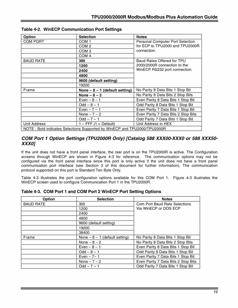
TPU2000/2000R Modbus/Modbus Plus Automation Guide
19
Table 4-2. WinECP Communication Port Settings
Option Selection NotesCOM PORT COM 1
COM 2COM 3COM 4
Personal Computer Port Selectionfor ECP to TPU2000 and TPU2000Rconnection.
BAUD RATE 3001200240048009600 (default setting)19200
Baud Rates Offered for TPU2000/2000R connection to theWinECP RS232 port connection.
Frame None – 8 – 1 (default setting) No Parity 8 Data Bits 1 Stop BitNone – 8 – 2 No Parity 8 Data Bits 2 Stop BitsEven – 8 – 1 Even Parity 8 Data Bits 1 Stop BitOdd – 8 – 1 Odd Parity 8 Data Bits 1 Stop BitEven – 7 – 1 Even Parity 7 Data Bits 1 Stop BitNone – 7 – 2 Even Parity 7 Data Bits 2 Stop BitsOdd – 7 – 1 Odd Parity 7 Data Bits 1 Stop Bit
Unit Address 1 – FFF (1 = Default) Unit Address in HEXNOTE : Bold indicates Selections Supported by WinECP and TPU2000/TPU2000R
COM Port 1 Option Settings (TPU2000R Only) [Catalog 588 XXX00-XXX0 or 588 XXX50-XXX0]
If the unit does not have a front panel interface, the rear port is on the TPU2000R is active. The Configurationscreens through WinECP are shown in Figure 4-3 for reference. The communication options may not beconfigured via the front panel interface since this port is only active if the unit does not have a front panelcommunication port interface (see Section 3 of this document for further information). The communicationprotocol supported on this port is Standard Ten Byte Only.
Table 4-3 illustrates the port configuration options available for this COM Port 1. Figure 4-3 illustrates theWinECP screen used to configure Communication Port 1 in the TPU2000R.
Table 4-3. COM Port 1 and COM Port 2 WinECP Port Setting Options
Option Selection NotesBAUD RATE 300
1200240048009600 (default setting)1920038400
Com Port Baud Rate SelectionsVia WinECP or DOS ECP
Frame None – 8 – 1 (default setting) No Parity 8 Data Bits 1 Stop BitNone – 8 – 2 No Parity 8 Data Bits 2 Stop BitsEven – 8 – 1 Even Parity 8 Data Bits 1 Stop BitOdd – 8 – 1 Odd Parity 8 Data Bits 1 Stop BitEven – 7– 1 Even Parity 7 Data Bits 1 Stop BitNone – 7 – 2 Even Parity 7 Data Bits 2 Stop BitsOdd – 7 – 1 Odd Parity 7 Data Bits 1 Stop Bit
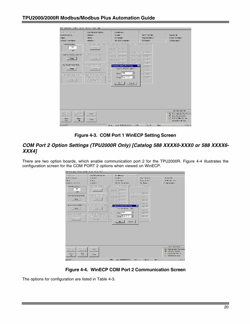
TPU2000/2000R Modbus/Modbus Plus Automation Guide
20
Figure 4-3. COM Port 1 WinECP Setting Screen
COM Port 2 Option Settings (TPU2000R Only) [Catalog 588 XXXX0-XXX0 or 588 XXXX6-XXX4]
There are two option boards, which enable communication port 2 for the TPU2000R. Figure 4-4 illustrates theconfiguration screen for the COM PORT 2 options when viewed on WinECP.
Figure 4-4. WinECP COM Port 2 Communication Screen
The options for configuration are listed in Table 4-3.
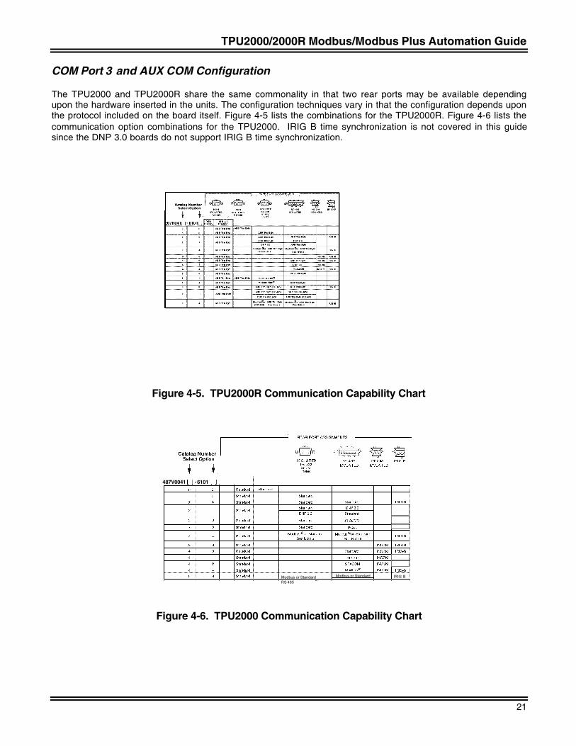
TPU2000/2000R Modbus/Modbus Plus Automation Guide
21
COM Port 3 and AUX COM Configuration
The TPU2000 and TPU2000R share the same commonality in that two rear ports may be available dependingupon the hardware inserted in the units. The configuration techniques vary in that the configuration depends uponthe protocol included on the board itself. Figure 4-5 lists the combinations for the TPU2000R. Figure 4-6 lists thecommunication option combinations for the TPU2000. IRIG B time synchronization is not covered in this guidesince the DNP 3.0 boards do not support IRIG B time synchronization.
Figure 4-5. TPU2000R Communication Capability Chart
IRIG BModbus or StandardModbus or StandardRS 485
487V0041 6101
Figure 4-6. TPU2000 Communication Capability Chart
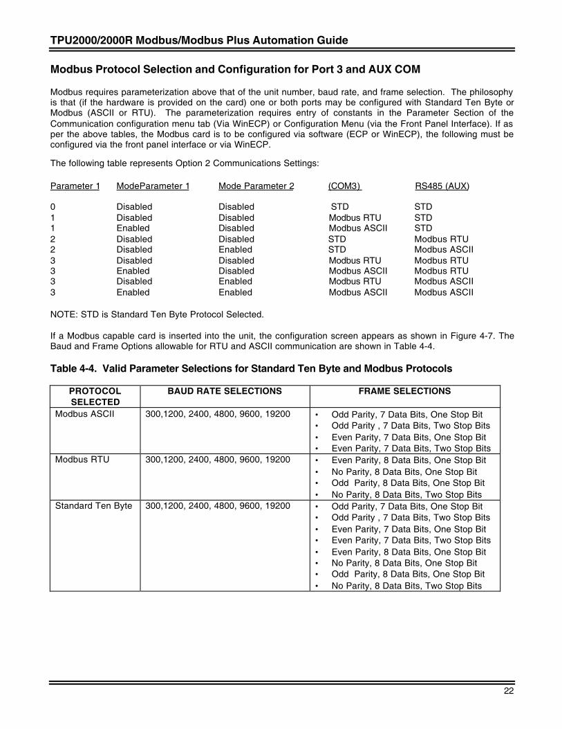
TPU2000/2000R Modbus/Modbus Plus Automation Guide
22
Modbus Protocol Selection and Configuration for Port 3 and AUX COM
Modbus requires parameterization above that of the unit number, baud rate, and frame selection. The philosophyis that (if the hardware is provided on the card) one or both ports may be configured with Standard Ten Byte orModbus (ASCII or RTU). The parameterization requires entry of constants in the Parameter Section of theCommunication configuration menu tab (Via WinECP) or Configuration Menu (via the Front Panel Interface). If asper the above tables, the Modbus card is to be configured via software (ECP or WinECP), the following must beconfigured via the front panel interface or via WinECP.
The following table represents Option 2 Communications Settings:
Parameter 1 ModeParameter 1 Mode Parameter 2 (COM3) RS485 (AUX)
0 Disabled Disabled STD STD1 Disabled Disabled Modbus RTU STD1 Enabled Disabled Modbus ASCII STD2 Disabled Disabled STD Modbus RTU2 Disabled Enabled STD Modbus ASCII3 Disabled Disabled Modbus RTU Modbus RTU3 Enabled Disabled Modbus ASCII Modbus RTU3 Disabled Enabled Modbus RTU Modbus ASCII3 Enabled Enabled Modbus ASCII Modbus ASCII
NOTE: STD is Standard Ten Byte Protocol Selected.
If a Modbus capable card is inserted into the unit, the configuration screen appears as shown in Figure 4-7. TheBaud and Frame Options allowable for RTU and ASCII communication are shown in Table 4-4.
Table 4-4. Valid Parameter Selections for Standard Ten Byte and Modbus Protocols
PROTOCOLSELECTED
BAUD RATE SELECTIONS FRAME SELECTIONS
Modbus ASCII 300,1200, 2400, 4800, 9600, 19200 • Odd Parity, 7 Data Bits, One Stop Bit• Odd Parity , 7 Data Bits, Two Stop Bits• Even Parity, 7 Data Bits, One Stop Bit• Even Parity, 7 Data Bits, Two Stop Bits
Modbus RTU 300,1200, 2400, 4800, 9600, 19200 • Even Parity, 8 Data Bits, One Stop Bit• No Parity, 8 Data Bits, One Stop Bit• Odd Parity, 8 Data Bits, One Stop Bit• No Parity, 8 Data Bits, Two Stop Bits
Standard Ten Byte 300,1200, 2400, 4800, 9600, 19200 • Odd Parity, 7 Data Bits, One Stop Bit• Odd Parity , 7 Data Bits, Two Stop Bits• Even Parity, 7 Data Bits, One Stop Bit• Even Parity, 7 Data Bits, Two Stop Bits• Even Parity, 8 Data Bits, One Stop Bit• No Parity, 8 Data Bits, One Stop Bit• Odd Parity, 8 Data Bits, One Stop Bit• No Parity, 8 Data Bits, Two Stop Bits
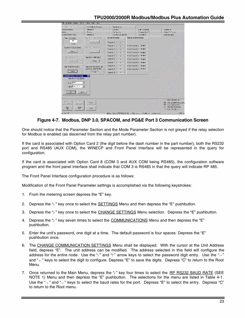
TPU2000/2000R Modbus/Modbus Plus Automation Guide
23
Figure 4-7. Modbus, DNP 3.0, SPACOM, and PG&E Port 3 Communication Screen
One should notice that the Parameter Section and the Mode Parameter Section is not greyed if the relay selectionfor Modbus is enabled (as discerned from the relay part number).
If the card is associated with Option Card 2 (the digit before the dash number in the part number), both the RS232port and RS485 (AUX COM), the WINECP and Front Panel Interface will be represented in the query forconfiguration.
If the card is associated with Option Card 8 (COM 3 and AUX COM being RS485), the configuration softwareprogram and the front panel interface shall indicate that COM 3 is RS485 in that the query will indicate RP 485.
The Front Panel Interface configuration procedure is as follows:
Modification of the Front Panel Parameter settings is accomplished via the following keystrokes:
1. From the metering screen depress the “E” key.
2. Depress the “↓” key once to select the SETTINGS Menu and then depress the “E” pushbutton.
3. Depress the “↓” key once to select the CHANGE SETTINGS Menu selection. Depress the “E” pushbutton.
4. Depress the “↓” key seven times to select the COMMUNICATIONS Menu and then depress the “E”pushbutton.
5. Enter the unit’s password, one digit at a time. The default password is four spaces. Depress the “E”pushbutton once.
6. The CHANGE COMMUNICATION SETTINGS Menu shall be displayed. With the cursor at the Unit Addressfield, depress “E”. The unit address can be modified. The address selected in this field will configure theaddress for the entire node. Use the “↓” and “↑” arrow keys to select the password digit entry. Use the “→”and “←” keys to select the digit to configure. Depress “E” to save the digits. Depress “C” to return to the RootMenu.
7. Once returned to the Main Menu, depress the “↓” key four times to select the RP RS232 BAUD RATE (SEENOTE 1) Menu and then depress the “E” pushbutton. The selections for the menu are listed in Table 4-1.Use the “→” and “←” keys to select the baud rates for the port. Depress “E” to select the entry. Depress “C”to return to the Root menu.
TPU2000/2000R Modbus/Modbus Plus Automation Guide
24
8. Once returned to the Main Menu, depress the “↓” key once to select the RP RS232 FRAME (SEE NOTE 2) Menu and then depress the “E” pushbutton. The selections for the menu are listed in Table 4-1. Use the “→” and “←” keys to select the baud rates for the port. Depress “E” to select the entry. Depress“C” to return to the Root Menu.
9. Once returned to the Main Menu, depress the “↓” key once to select the RP RS485 BAUD RATE (SEE NOTE3) menu and then depress the “E” pushbutton. The selections for the menu are listed in Table 4-1. Use the“→” and “←” keys to select the baud rates for the port. Depress “E” to select the entry. Depress “C” to returnto the Root Menu.
10. Once returned to the main menu, depress the “↓” key once to select the RP RS485 FRAME (SEE NOTE 4)menu and then depress the “E” pushbutton. The selections for the menu are listed in Table 4-1. Use the “→”and “←” keys to select the baud rates for the port. Depress “E” to select the entry. Depress “C” to return tothe Root Menu.
11. Once returned to the Main Menu, depress the “↓” key once to select the RP IRIG B selection. Refer toSection 5 to determine the configuration for the IRIG B of the unit.
12. Once returned to the Main Menu, depress the “↓” key once to select the PARAMETER 1 Menu and thendepress the “E” pushbutton. The selections for this field may range from 0 to 255. Use the “→” and “←” keysto select appropriate entry for Parameter 1 as described above. Depress “E” to select the entry. Depress “C”to return to the Root Menu.
13. Once returned to the Main Menu, depress the “↓” key twelve times to select the MODE PARAMETER 1 Menuitem and then depress the “E” pushbutton. The selections for this field are enable and disable. Use the “→”and “←” keys to select appropriate entry for MODE PARAMETER 1 as described above. Depress “E” toselect the entry. Depress “C” to return to the Root Menu.
14. Once returned to the Main Menu, depress the “↓” key once to select the MODE PARAMETER 2 Menu itemand then depress the “E” pushbutton. The selections for this field are enable and disable. Use the “→” and“←” keys to select appropriate entry for MODE PARAMETER 1 as described above. Depress “E” to selectthe entry. Depress “C” to return to the Root Menu.
15. To Save the selections configured in the previous steps depress the “C” pushbutton. A query will bepresented to the operator “Enter YES to save settings <NO>”. Use the “→” and “←” keys to select the optionYES and depress “E” to save the settings.
NOTE 1: If the DUAL RS485 Board (Option 8) is selected, the query shall be modified as: RS485 – 1Baud. If the hardware does not support COM 3, this query shall be omitted.
NOTE 2: If the DUAL RS485 Board (Option 8) is selected, the query shall be modified as RS485 – 1Frame. If the hardware does not support COM 3, this query shall be omitted.
NOTE 3: If the DUAL RS485 Board (Option 8) is selected, the query shall be modified to RS485 – 2Baud.
NOTE 4: If the DUAL RS485 Board (Option 8) is selected, the query shall be modified to RS485 – 2Frame.
Modbus Plus Port Configuration [COM 3 on Selected Units] (TPU2000R Only)
Only the TPU2000R supports Modbus Plus. The TPU2000R recognizes if the communication card supportsModbus Plus. Only the Unit Address field within the communication port parameter screen is used via ModbusPlus. One should refer later sections in this manual for a further explanation of the Modbus Plus addressingscheme for accessing relay information.
IRIG B Configuration and Wiring
Although not a protocol, IRIG B time synchronization is included on the communication cards within the TPU2000and TPU2000R. The following section describes the theory, connection and configuration options present withinthe TPU2000 and TPU2000R.
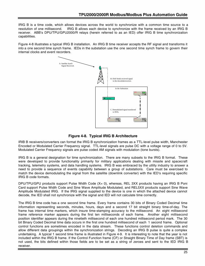
TPU2000/2000R Modbus/Modbus Plus Automation Guide
25
IRIG B is a time code, which allows devices across the world to synchronize with a common time source to aresolution of one millisecond. IRIG B allows each device to synchronize with the frame received by an IRIG Breceiver. ABB’s DPU/TPU/GPU2000/R relays (herein referred to as an IED) offer IRIG B time synchronizationcapabilities.
Figure 4-8 illustrates a typical IRIG B installation. An IRIG B time receiver accepts the RF signal and transforms itinto a one second time synch frame. IEDs in the substation use the one second time synch frame to govern theirinternal clocks and event recorders.
In the Substation
True Time
EC
EC
EC
A. Satellite Synch Signal Received.
B. Dish Sends received signal to the downlink/receiver.
C. Demodulated signal transferred to IEDs.
Figure 4-8. Typical IRIG B ArchitectureIRIB B receivers/converters can format the IRIG B synchronization frames as a TTL-level pulse width, ManchesterEncoded or Modulated Carrier Frequency signal. TTL-level signals are pulse DC with a voltage range of 0 to 5V.Modulated Carrier Frequency signals are pulse coded AM signals with modulation (tone bursts).
IRIG B is a general designation for time synchronization. There are many subsets to the IRIG B format. Thesewere developed to provide functionality primarily for military applications dealing with missile and spacecrafttracking, telemetry systems, and data handling systems. IRIG B was embraced by the utility industry to answer aneed to provide a sequence of events capability between a group of substations. Care must be exercised tomatch the device demodulating the signal from the satellite (downlink converter) with the IED’s requiring specificIRIG B code formats.
DPU/TPU/GPU products support Pulse Width Code (X= 0), whereas, REL 3XX products having an IRIG B PoniCard support Pulse Width Code and Sine Wave Amplitude Modulated, and REL5XX products support Sine WaveAmplitude Modulated IRIG. If the IRIG signal supplied to the device is one in which the attached device cannotdecode, the IED shall not synchronize with the signal and IED will not calculate time correctly.
The IRIG B time code has a one second time frame. Every frame contains 30 bits of Binary Coded Decimal timeinformation representing seconds, minutes, hours, days and a second 17 bit straight binary time-of-day. Theframe has internal time markers, which insure time-stamping accuracy to the millisecond. An eight millisecondframe reference marker appears during the first ten milliseconds of each frame. Another eight millisecondposition identifier appears during the ninetieth millisecond of each one hundred millisecond period mark. The 30bit Binary Coded Decimal time data occurs in the first one hundred millisecond of each 1 second frame. Optionalcontrol functions are sometimes encoded in the data stream. These functions control deletion commands andallow different data groupings within the synchronization strings. Decoding an IRIG B pulse is quite a complexundertaking. A typical 1 second time frame is illustrated in Figure 4-9. It is interesting to note that the year is notincluded within the IRIG B frame. If the Control Function frame (CF) or Straight Binary Time of Day frame (SBT) isnot used, the bits defined within those fields are to be set as a string of zeroes and sent to the IED IRIG Breceiver.
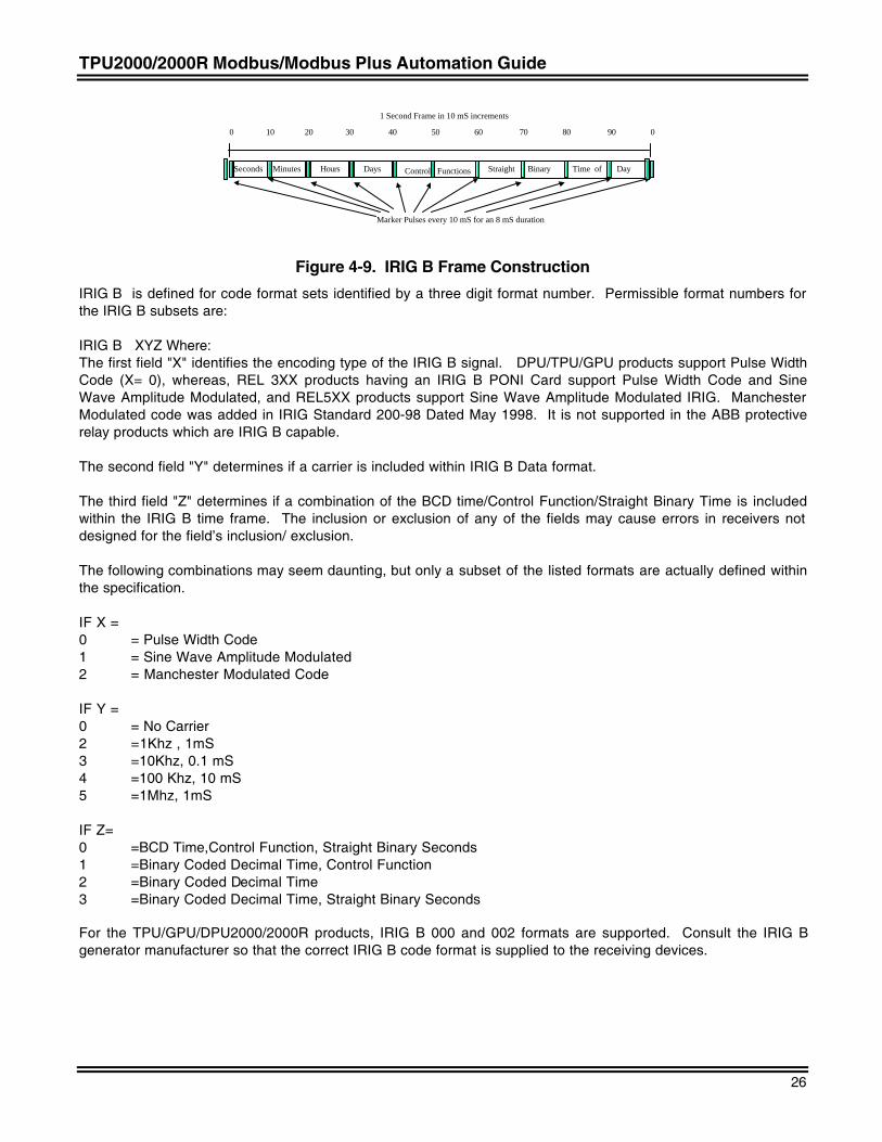
TPU2000/2000R Modbus/Modbus Plus Automation Guide
26
Seconds Minutes Hours Days Control Functions Straight Binary Time of Day
0 10 20 30 40 50 60 70 80 90 0
Marker Pulses every 10 mS for an 8 mS duration
1 Second Frame in 10 mS increments
Figure 4-9. IRIG B Frame Construction
IRIG B is defined for code format sets identified by a three digit format number. Permissible format numbers forthe IRIG B subsets are:
IRIG B XYZ Where:The first field "X" identifies the encoding type of the IRIG B signal. DPU/TPU/GPU products support Pulse WidthCode (X= 0), whereas, REL 3XX products having an IRIG B PONI Card support Pulse Width Code and SineWave Amplitude Modulated, and REL5XX products support Sine Wave Amplitude Modulated IRIG. ManchesterModulated code was added in IRIG Standard 200-98 Dated May 1998. It is not supported in the ABB protectiverelay products which are IRIG B capable.
The second field "Y" determines if a carrier is included within IRIG B Data format.
The third field "Z" determines if a combination of the BCD time/Control Function/Straight Binary Time is includedwithin the IRIG B time frame. The inclusion or exclusion of any of the fields may cause errors in receivers notdesigned for the field’s inclusion/ exclusion.
The following combinations may seem daunting, but only a subset of the listed formats are actually defined withinthe specification.
IF X =0 = Pulse Width Code1 = Sine Wave Amplitude Modulated2 = Manchester Modulated Code
IF Y =0 = No Carrier2 =1Khz , 1mS3 =10Khz, 0.1 mS4 =100 Khz, 10 mS5 =1Mhz, 1mS
IF Z=0 =BCD Time,Control Function, Straight Binary Seconds1 =Binary Coded Decimal Time, Control Function2 =Binary Coded Decimal Time3 =Binary Coded Decimal Time, Straight Binary Seconds
For the TPU/GPU/DPU2000/2000R products, IRIG B 000 and 002 formats are supported. Consult the IRIG Bgenerator manufacturer so that the correct IRIG B code format is supplied to the receiving devices.
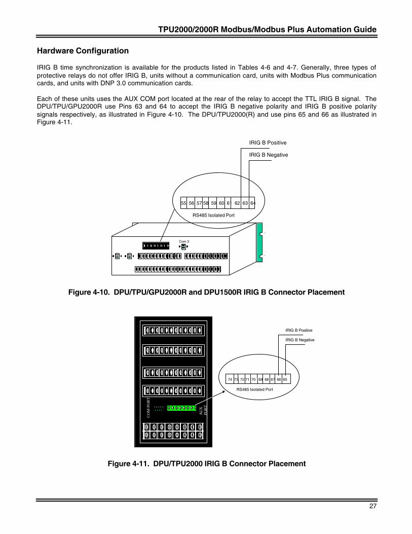
TPU2000/2000R Modbus/Modbus Plus Automation Guide
27
Hardware Configuration
IRIG B time synchronization is available for the products listed in Tables 4-6 and 4-7. Generally, three types ofprotective relays do not offer IRIG B, units without a communication card, units with Modbus Plus communicationcards, and units with DNP 3.0 communication cards.
Each of these units uses the AUX COM port located at the rear of the relay to accept the TTL IRIG B signal. TheDPU/TPU/GPU2000R use Pins 63 and 64 to accept the IRIG B negative polarity and IRIG B positive polaritysignals respectively, as illustrated in Figure 4-10. The DPU/TPU2000(R) and use pins 65 and 66 as illustrated inFigure 4-11.
Com 3
55 56 57 58 59 60 61 62 63 64
RS485 Isolated Port
IRIG B Positive
IRIG B Negative
Figure 4-10. DPU/TPU/GPU2000R and DPU1500R IRIG B Connector Placement
CO
M P
OR
T
AU
XPO
RT
74 73 72 71 70 69 68 67 66 65
RS485 Isolated Port
IRIG B Positive
IRIG B Negative
Figure 4-11. DPU/TPU2000 IRIG B Connector Placement
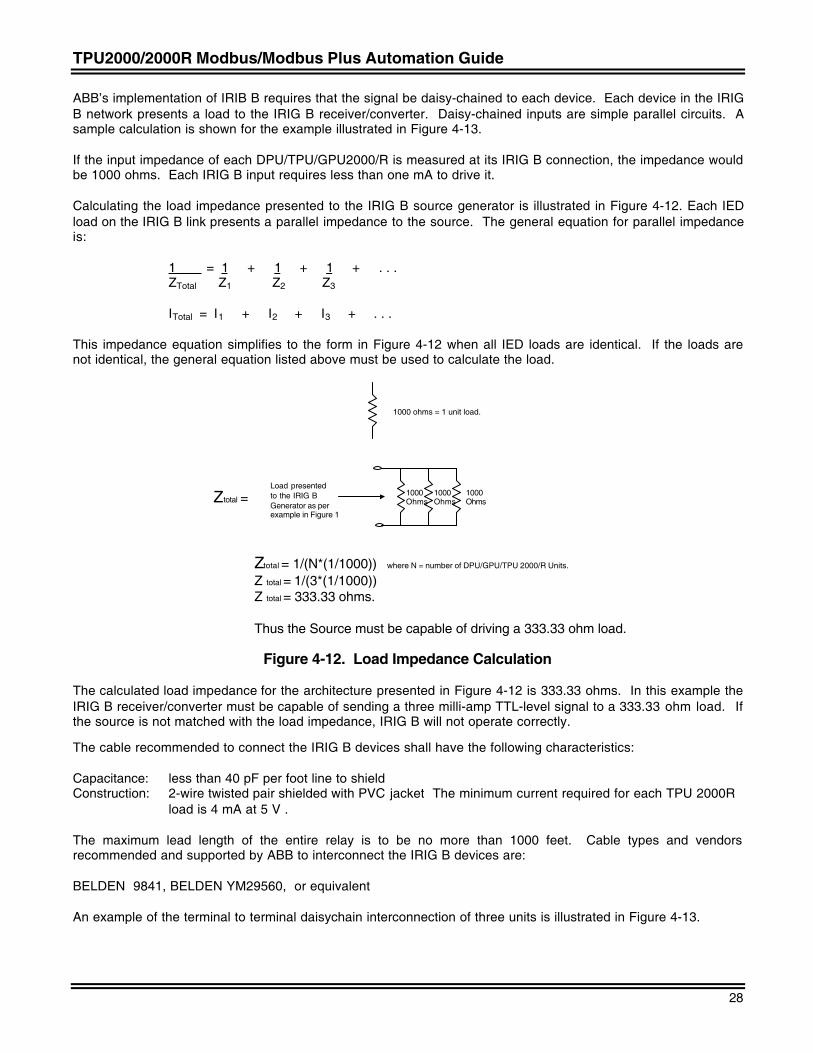
TPU2000/2000R Modbus/Modbus Plus Automation Guide
28
ABB’s implementation of IRIB B requires that the signal be daisy-chained to each device. Each device in the IRIGB network presents a load to the IRIG B receiver/converter. Daisy-chained inputs are simple parallel circuits. Asample calculation is shown for the example illustrated in Figure 4-13.
If the input impedance of each DPU/TPU/GPU2000/R is measured at its IRIG B connection, the impedance wouldbe 1000 ohms. Each IRIG B input requires less than one mA to drive it.
Calculating the load impedance presented to the IRIG B source generator is illustrated in Figure 4-12. Each IEDload on the IRIG B link presents a parallel impedance to the source. The general equation for parallel impedanceis:
1 = 1 + 1 + 1 + . . .ZTotal Z1 Z2 Z3
ITotal = I1 + I2 + I3 + . . .
This impedance equation simplifies to the form in Figure 4-12 when all IED loads are identical. If the loads arenot identical, the general equation listed above must be used to calculate the load.
1000 ohms = 1 unit load.
Load presentedto the IRIG BGenerator as perexample in Figure 1
1000Ohms
1000Ohms
1000Ohms
Ztotal = 1/(N*(1/1000)) where N = number of DPU/GPU/TPU 2000/R Units.
Z total = 1/(3*(1/1000))Z total = 333.33 ohms.
Thus the Source must be capable of driving a 333.33 ohm load.
Ztotal =
Figure 4-12. Load Impedance Calculation
The calculated load impedance for the architecture presented in Figure 4-12 is 333.33 ohms. In this example theIRIG B receiver/converter must be capable of sending a three milli-amp TTL-level signal to a 333.33 ohm load. Ifthe source is not matched with the load impedance, IRIG B will not operate correctly.
The cable recommended to connect the IRIG B devices shall have the following characteristics:
Capacitance: less than 40 pF per foot line to shieldConstruction: 2-wire twisted pair shielded with PVC jacket The minimum current required for each TPU 2000R
load is 4 mA at 5 V .
The maximum lead length of the entire relay is to be no more than 1000 feet. Cable types and vendorsrecommended and supported by ABB to interconnect the IRIG B devices are:
BELDEN 9841, BELDEN YM29560, or equivalent
An example of the terminal to terminal daisychain interconnection of three units is illustrated in Figure 4-13.
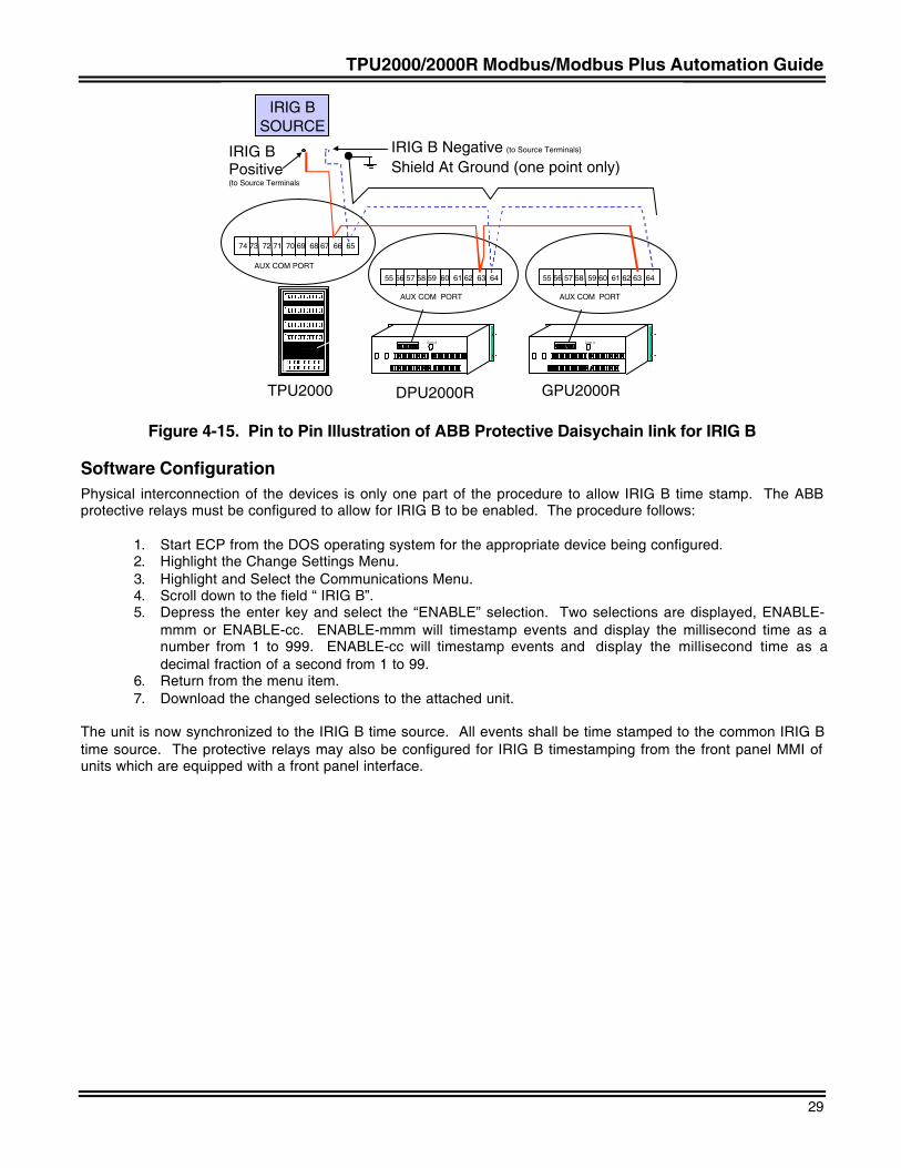
TPU2000/2000R Modbus/Modbus Plus Automation Guide
29
74 73 72 71 70 69 68 67 66 65
AUX COM PORT
IRIG BSOURCE
TPU2000
Com 3
55 56 57 58 59 60 61 62 63 64
AUX COM PORT
DPU2000R
Com 3
55 56 57 58 59 60 61 62 63 64
AUX COM PORT
GPU2000R
IRIG B Negative (to Source Terminals)IRIG BPositive(to Source Terminals
Shield At Ground (one point only)
Figure 4-15. Pin to Pin Illustration of ABB Protective Daisychain link for IRIG B
Software ConfigurationPhysical interconnection of the devices is only one part of the procedure to allow IRIG B time stamp. The ABBprotective relays must be configured to allow for IRIG B to be enabled. The procedure follows:
1. Start ECP from the DOS operating system for the appropriate device being configured.2. Highlight the Change Settings Menu.3. Highlight and Select the Communications Menu.4. Scroll down to the field “ IRIG B”.5. Depress the enter key and select the “ENABLE” selection. Two selections are displayed, ENABLE-
mmm or ENABLE-cc. ENABLE-mmm will timestamp events and display the millisecond time as anumber from 1 to 999. ENABLE-cc will timestamp events and display the millisecond time as adecimal fraction of a second from 1 to 99.
6. Return from the menu item.7. Download the changed selections to the attached unit.
The unit is now synchronized to the IRIG B time source. All events shall be time stamped to the common IRIG Btime source. The protective relays may also be configured for IRIG B timestamping from the front panel MMI ofunits which are equipped with a front panel interface.
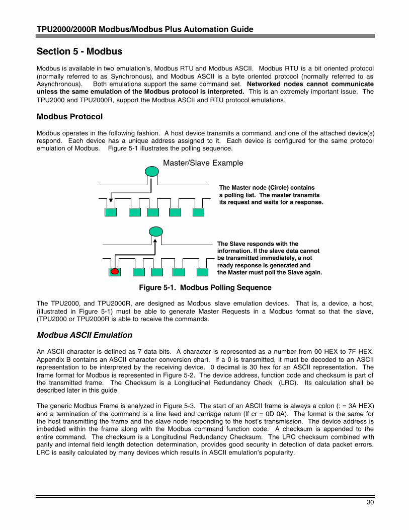
TPU2000/2000R Modbus/Modbus Plus Automation Guide
30
Section 5 - Modbus
Modbus is available in two emulation’s, Modbus RTU and Modbus ASCII. Modbus RTU is a bit oriented protocol(normally referred to as Synchronous), and Modbus ASCII is a byte oriented protocol (normally referred to asAsynchronous). Both emulations support the same command set. Networked nodes cannot communicateunless the same emulation of the Modbus protocol is interpreted. This is an extremely important issue. TheTPU2000 and TPU2000R, support the Modbus ASCII and RTU protocol emulations.
Modbus Protocol
Modbus operates in the following fashion. A host device transmits a command, and one of the attached device(s)respond. Each device has a unique address assigned to it. Each device is configured for the same protocolemulation of Modbus. Figure 5-1 illustrates the polling sequence.
Master/Slave Example
The Master node (Circle) containsa polling list. The master transmitsits request and waits for a response.
The Slave responds with the information. If the slave data cannot be transmitted immediately, a not ready response is generated and the Master must poll the Slave again.
Figure 5-1. Modbus Polling Sequence
The TPU2000, and TPU2000R, are designed as Modbus slave emulation devices. That is, a device, a host,(illustrated in Figure 5-1) must be able to generate Master Requests in a Modbus format so that the slave,(TPU2000 or TPU2000R is able to receive the commands.
Modbus ASCII Emulation
An ASCII character is defined as 7 data bits. A character is represented as a number from 00 HEX to 7F HEX.Appendix B contains an ASCII character conversion chart. If a 0 is transmitted, it must be decoded to an ASCIIrepresentation to be interpreted by the receiving device. 0 decimal is 30 hex for an ASCII representation. Theframe format for Modbus is represented in Figure 5-2. The device address, function code and checksum is part ofthe transmitted frame. The Checksum is a Longitudinal Redundancy Check (LRC). Its calculation shall bedescribed later in this guide.
The generic Modbus Frame is analyzed in Figure 5-3. The start of an ASCII frame is always a colon (: = 3A HEX)and a termination of the command is a line feed and carriage return (lf cr = 0D 0A). The format is the same forthe host transmitting the frame and the slave node responding to the host’s transmission. The device address isimbedded within the frame along with the Modbus command function code. A checksum is appended to theentire command. The checksum is a Longitudinal Redundancy Checksum. The LRC checksum combined withparity and internal field length detection determination, provides good security in detection of data packet errors.LRC is easily calculated by many devices which results in ASCII emulation’s popularity.
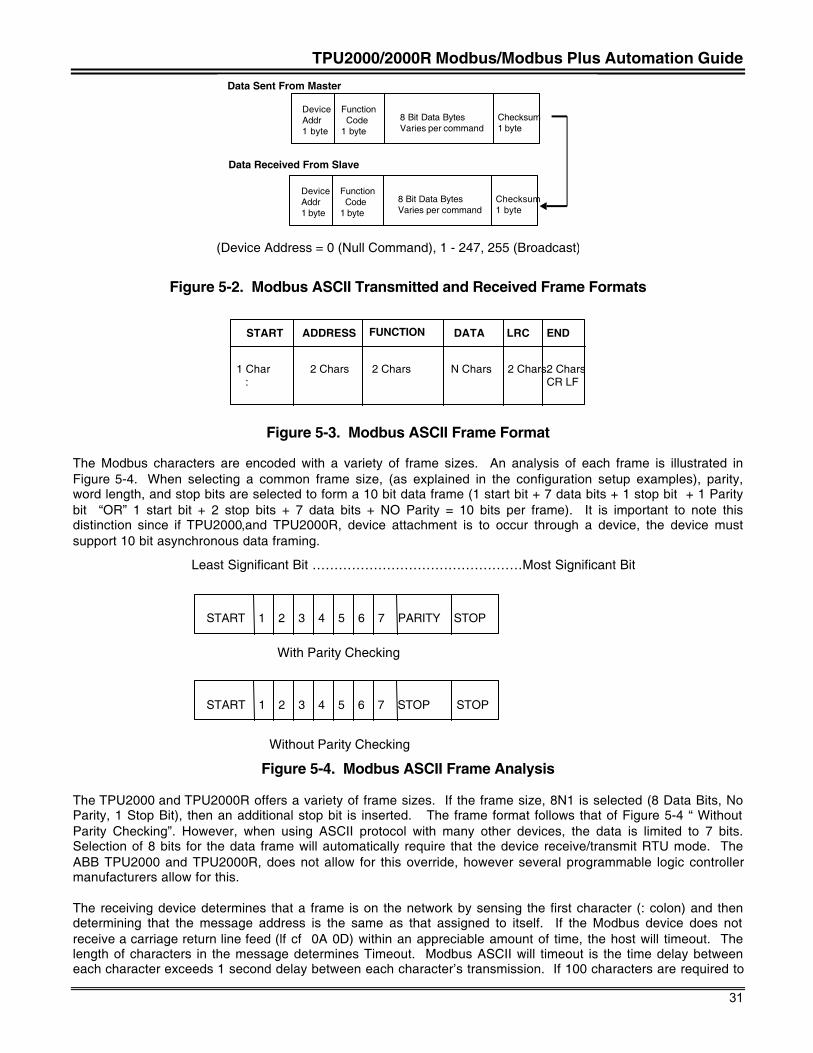
TPU2000/2000R Modbus/Modbus Plus Automation Guide
31
DeviceAddr1 byte
Function Code1 byte
8 Bit Data BytesVaries per command
Checksum1 byte
DeviceAddr1 byte
Function Code1 byte
8 Bit Data BytesVaries per command
Checksum1 byte
Data Sent From Master
Data Received From Slave
(Device Address = 0 (Null Command), 1 - 247, 255 (Broadcast)
Figure 5-2. Modbus ASCII Transmitted and Received Frame Formats
START FUNCTIONADDRESS DATA LRC END
1 Char :
2 Chars 2 Chars N Chars 2 Chars2 CharsCR LF
Figure 5-3. Modbus ASCII Frame Format
The Modbus characters are encoded with a variety of frame sizes. An analysis of each frame is illustrated inFigure 5-4. When selecting a common frame size, (as explained in the configuration setup examples), parity,word length, and stop bits are selected to form a 10 bit data frame (1 start bit + 7 data bits + 1 stop bit + 1 Paritybit “OR” 1 start bit + 2 stop bits + 7 data bits + NO Parity = 10 bits per frame). It is important to note thisdistinction since if TPU2000,and TPU2000R, device attachment is to occur through a device, the device mustsupport 10 bit asynchronous data framing.
Least Significant Bit …………………………………………Most Significant Bit
START 1 2 3 4 5 6 7 PARITY STOP
With Parity Checking
START 1 2 3 4 5 6 7 STOP STOP
Without Parity Checking
Figure 5-4. Modbus ASCII Frame Analysis
The TPU2000 and TPU2000R offers a variety of frame sizes. If the frame size, 8N1 is selected (8 Data Bits, NoParity, 1 Stop Bit), then an additional stop bit is inserted. The frame format follows that of Figure 5-4 “ WithoutParity Checking”. However, when using ASCII protocol with many other devices, the data is limited to 7 bits.Selection of 8 bits for the data frame will automatically require that the device receive/transmit RTU mode. TheABB TPU2000 and TPU2000R, does not allow for this override, however several programmable logic controllermanufacturers allow for this.
The receiving device determines that a frame is on the network by sensing the first character (: colon) and thendetermining that the message address is the same as that assigned to itself. If the Modbus device does notreceive a carriage return line feed (lf cf 0A 0D) within an appreciable amount of time, the host will timeout. Thelength of characters in the message determines Timeout. Modbus ASCII will timeout is the time delay betweeneach character exceeds 1 second delay between each character’s transmission. If 100 characters are required to
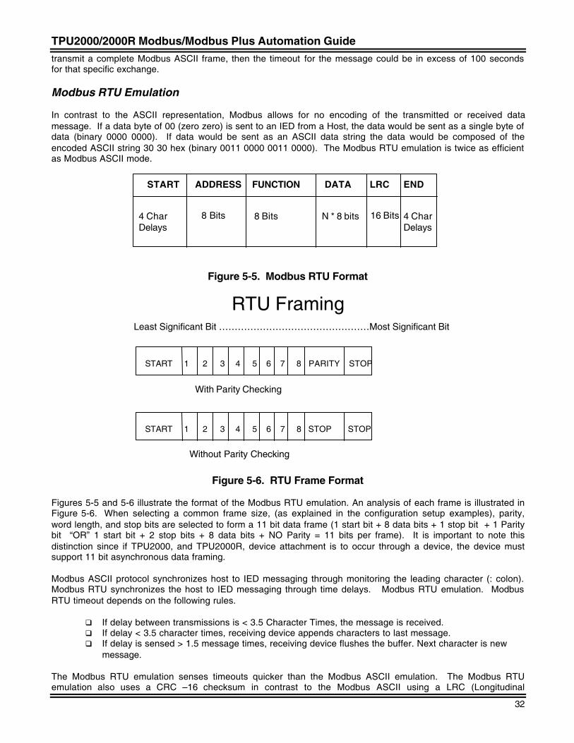
TPU2000/2000R Modbus/Modbus Plus Automation Guide
32
transmit a complete Modbus ASCII frame, then the timeout for the message could be in excess of 100 secondsfor that specific exchange.
Modbus RTU Emulation
In contrast to the ASCII representation, Modbus allows for no encoding of the transmitted or received datamessage. If a data byte of 00 (zero zero) is sent to an IED from a Host, the data would be sent as a single byte ofdata (binary 0000 0000). If data would be sent as an ASCII data string the data would be composed of theencoded ASCII string 30 30 hex (binary 0011 0000 0011 0000). The Modbus RTU emulation is twice as efficientas Modbus ASCII mode.
START FUNCTIONADDRESS DATA LRC END
4 CharDelays
8 Bits 8 Bits N * 8 bits 16 Bits 4 CharDelays
Figure 5-5. Modbus RTU Format
RTU FramingLeast Significant Bit …………………………………………Most Significant Bit
With Parity Checking
Without Parity Checking
START 1 2 3 4 5 6 7 8 PARITY STOP
START 1 2 3 4 5 6 7 8 STOP STOP
Figure 5-6. RTU Frame Format
Figures 5-5 and 5-6 illustrate the format of the Modbus RTU emulation. An analysis of each frame is illustrated inFigure 5-6. When selecting a common frame size, (as explained in the configuration setup examples), parity,word length, and stop bits are selected to form a 11 bit data frame (1 start bit + 8 data bits + 1 stop bit + 1 Paritybit “OR” 1 start bit + 2 stop bits + 8 data bits + NO Parity = 11 bits per frame). It is important to note thisdistinction since if TPU2000, and TPU2000R, device attachment is to occur through a device, the device mustsupport 11 bit asynchronous data framing.
Modbus ASCII protocol synchronizes host to IED messaging through monitoring the leading character (: colon).Modbus RTU synchronizes the host to IED messaging through time delays. Modbus RTU emulation. ModbusRTU timeout depends on the following rules.
q If delay between transmissions is < 3.5 Character Times, the message is received.q If delay < 3.5 character times, receiving device appends characters to last message.q If delay is sensed > 1.5 message times, receiving device flushes the buffer. Next character is new
message.
The Modbus RTU emulation senses timeouts quicker than the Modbus ASCII emulation. The Modbus RTUemulation also uses a CRC –16 checksum in contrast to the Modbus ASCII using a LRC (Longitudinal
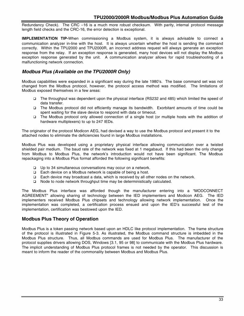
TPU2000/2000R Modbus/Modbus Plus Automation Guide
33
Redundancy Check). The CRC –16 is a much more robust checksum. With parity, internal protocol messagelength field checks and the CRC-16, the error detection is exceptional.
IMPLEMENTATION TIP-When commissioning a Modbus system, it is always advisable to connect acommunication analyzer in-line with the host. It is always uncertain whether the host is sending the commandcorrectly. Within the TPU2000 and TPU2000R, an incorrect address request will always generate an exceptionresponse from the relay. If an exception response is generated, many host devices will not display the Modbusexception response generated by the unit. A communication analyzer allows for rapid troubleshooting of amalfunctioning network connection.
Modbus Plus (Available on the TPU2000R Only)
Modbus capabilities were expanded in a significant way during the late 1980’s. The base command set was notchanged from the Modbus protocol, however, the protocol access method was modified. The limitations ofModbus exposed themselves in a few areas:
q The throughput was dependent upon the physical interface (RS232 and 485) which limited the speed ofdata transfer.
q The Modbus protocol did not efficiently manage its bandwidth. Exorbitant amounts of time could bespent waiting for the slave device to respond with data or timeout.
q The Modbus protocol only allowed connection of a single host (or multiple hosts with the addition ofhardware multiplexers) to up to 247 IEDs.
The originator of the protocol Modicon AEG, had devised a way to use the Modbus protocol and present it to theattached nodes to eliminate the deficiencies found in large Modbus installations.
Modbus Plus was developed using a proprietary physical interface allowing communication over a twistedshielded pair medium. The baud rate of the network was fixed at 1 megabaud. If this had been the only changefrom Modbus to Modbus Plus, the network’s introduction would not have been significant. The Modbusrepackaging into a Modbus Plus format afforded the following significant benefits:
q Up to 34 simultaneous conversations may occur on a network.q Each device on a Modbus network is capable of being a host.q Each device may broadcast a data, which is received by all other nodes on the network.q Node to node network throughput time may be deterministically calculated.
The Modbus Plus interface was afforded though the manufacturer entering into a “MODCONNECTAGREEMENT” allowing sharing of technology between the IED implementers and Modicon AEG. The IEDimplementers received Modbus Plus chipsets and technology allowing network implementation. Once theimplementation was completed, a certification process ensued and upon the IED’s successful test of theimplementation, certification was bestowed upon the IED.
Modbus Plus Theory of Operation
Modbus Plus is a token passing network based upon an HDLC like protocol implementation. The frame structureof the protocol is illustrated in Figure 5-3. As illustrated, the Modbus command structure is imbedded in theModbus Plus structure. Thus, all Modbus commands are used for Modbus Plus. The manufacturer of theprotocol supplies drivers allowing DOS, Windows [3.1, 95 or 98] to communicate with the Modbus Plus hardware.The implicit understanding of Modbus Plus protocol frames is not needed by the operator. This discussion ismeant to inform the reader of the commonality between Modbus and Modbus Plus.
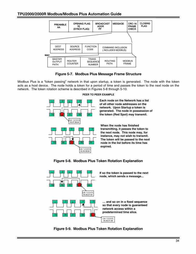
TPU2000/2000R Modbus/Modbus Plus Automation Guide
34
PREAMBLE AA
OPENING FLAG 7E(SYNCH FLAG)
BROADCAST ADDR FF
CRC-16FRAMECHECK
CLOSING FLAG
MESSAGEPREAMBLE AA
OPENING FLAG 7E(SYNCH FLAG)
BROADCAST ADDR FF
CRC-16FRAMECHECK
CLOSING FLAG
MESSAGE
DEST ADDRESS
SOURCEADDRESS
FUNCTION CODE
COMMAND INCLUSION( INCLUDES MODBUS)
MASTEROUTPUTPATH
ROUTERCOUNTER
TRANSSEQUENCE NUMBER
ROUTING PATH
MODBUS FRAME
MAC
Figure 5-7. Modbus Plus Message Frame Structure
Modbus Plus is a “token passing” network in that upon startup, a token is generated. The node with the tokenacts as a host device. The node holds a token for a period of time and passes the token to the next node on thenetwork. The token rotation scheme is described in Figures 5-8 through 5-10.
PEER TO PEER EXAMPLE
Each node on the Network has a list of all other node addresses on the network. Upon Startup a token isgenerated. The node in possession ofthe token (Red Spot) may transmit.
When the node has finishedtransmitting, it passes the token tothe next node. This node may, for instance, may not wish to transmit. The token will be passed to the next node in the list before its time has expired.
1 2 3 4 5
55 57 58 64
1 2 3 4 5
55 57 58 6456
List: 1,2,3,4,5,55,57,58,64
List: 1,2,3,4,5,55,56,58,64
56
Figure 5-8. Modbus Plus Token Rotation Explanation
If so the token is passed to the next node, which sends a message...
… and so on in a fixed sequence so that every node is guaranteed network access within a predetermined time slice.
1 2 3 4 5
55 57 6456 58
1 2 3 4 5
55 5756 58 64
List: 1,2,3,4,5,55,56,57,64
List: 1,2,3,4,5,55,56,57,58
Figure 5-9. Modbus Plus Token Rotation Explanation
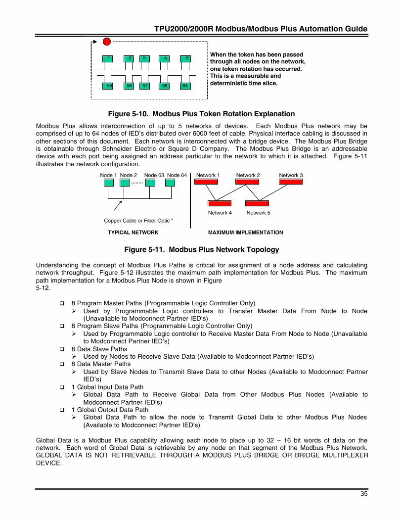
TPU2000/2000R Modbus/Modbus Plus Automation Guide
35
1 2 3 4 5
55 5756 58 64
When the token has been passed through all nodes on the network, one token rotation has occurred. This is a measurable and deterministic time slice.
Figure 5-10. Modbus Plus Token Rotation Explanation
Modbus Plus allows interconnection of up to 5 networks of devices. Each Modbus Plus network may becomprised of up to 64 nodes of IED’s distributed over 6000 feet of cable. Physical interface cabling is discussed inother sections of this document. Each network is interconnected with a bridge device. The Modbus Plus Bridgeis obtainable through Schneider Electric or Square D Company. The Modbus Plus Bridge is an addressabledevice with each port being assigned an address particular to the network to which it is attached. Figure 5-11illustrates the network configuration.
Node 1 Node 2 Node 63 Node 64
Copper Cable or Fiber Optic *
Network 1 Network 2 Network 3
Network 4 Network 5
TYPICAL NETWORK MAXIMUM IMPLEMENTATION
Figure 5-11. Modbus Plus Network Topology
Understanding the concept of Modbus Plus Paths is critical for assignment of a node address and calculatingnetwork throughput. Figure 5-12 illustrates the maximum path implementation for Modbus Plus. The maximumpath implementation for a Modbus Plus Node is shown in Figure5-12.
q 8 Program Master Paths (Programmable Logic Controller Only)Ø Used by Programmable Logic controllers to Transfer Master Data From Node to Node
(Unavailable to Modconnect Partner IED’s)q 8 Program Slave Paths (Programmable Logic Controller Only)Ø Used by Programmable Logic controller to Receive Master Data From Node to Node (Unavailable
to Modconnect Partner IED’s)q 8 Data Slave PathsØ Used by Nodes to Receive Slave Data (Available to Modconnect Partner IED’s)
q 8 Data Master PathsØ Used by Slave Nodes to Transmit Slave Data to other Nodes (Available to Modconnect Partner
IED’s)q 1 Global Input Data PathØ Global Data Path to Receive Global Data from Other Modbus Plus Nodes (Available to
Modconnect Partner IED’s)q 1 Global Output Data PathØ Global Data Path to allow the node to Transmit Global Data to other Modbus Plus Nodes
(Available to Modconnect Partner IED’s)
Global Data is a Modbus Plus capability allowing each node to place up to 32 – 16 bit words of data on thenetwork. Each word of Global Data is retrievable by any node on that segment of the Modbus Plus Network.GLOBAL DATA IS NOT RETRIEVABLE THROUGH A MODBUS PLUS BRIDGE OR BRIDGE MULTIPLEXERDEVICE.
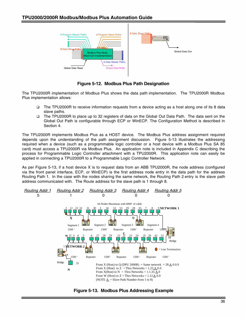
TPU2000/2000R Modbus/Modbus Plus Automation Guide
36
Modbus Plus Node (Maximum Implementation)
8 Data Master Paths
8 Data Slave Paths
Global Data Read Global Data Write
8 Program Master Paths 8 Program Slave Paths
EC
8 Data Slave Paths
Global Data Out
Figure 5-12. Modbus Plus Path Designation
The TPU2000R implementation of Modbus Plus shows the data path implementation. The TPU2000R ModbusPlus implementation allows:
q The TPU2000R to receive information requests from a device acting as a host along one of its 8 dataslave paths.
q The TPU2000R to place up to 32 registers of data on the Global Out Data Path. The data sent on theGlobal Out Path is configurable through ECP or WinECP. The Configuration Method is described inSection 4.
The TPU2000R implements Modbus Plus as a HOST device. The Modbus Plus address assignment requireddepends upon the understanding of the path assignment discussion. Figure 5-13 illustrates the addressingrequired when a device (such as a programmable logic controller or a host device with a Modbus Plus SA 85card) must access a TPU2000R via Modbus Plus. An application note is included in Appendix C describing theprocess for Programmable Logic Controller attachment with a TPU2000R. This application note can easily beapplied in connecting a TPU2000R to a Programmable Logic Controller Network.
As per Figure 5-13, if a host device X is to request data from an ABB TPU2000R, the node address (configuredvia the front panel interface, ECP, or WinECP) is the first address node entry in the data path for the addressRouting Path 1. In the case with the nodes sharing the same network, the Routing Path 2 entry is the slave pathaddress communicated with. The Route address for the slave path is 1 through 8.
Routing Addr 1 Routing Addr 2 Routing Addr 3 Routing Addr 4 Routing Addr 55 1 0 0 0
64 Nodes Maximum with 6000’ of cable
1500 ‘ Repeater 1500’ Repeater 1500 ‘ Repeater 1500 ‘
1500 ‘ Repeater 1500’ Repeater 1500 ‘ Repeater 1500 ‘
Bridge
Bridge
1
64
1
64
12
3 4 5 6 27 28 29 21 22 23 24 25 26 42 52
2
12
22 32
Segment 1 Segment 2 Segment 3 Segment 4
= Line Termination
31 30 3 34 52 53 29 28 35 7 8 9 NETWORK 1
NETWORK 2
X Q
ZW
From X (Host) to Q (DPU 2000R) = Same network = 28.A.0.0.0From X (Host) to Z = Thru Networks = 1.22.A.0.0From X(Host) to N = Thru Networks = 1.1.33.A.0From W (Host) to Z = Thru Networks = 1.12.A.0.0(NOTE A = Slave Path Number from 1 to 8)
33
N
Figure 5-13. Modbus Plus Addressing Example
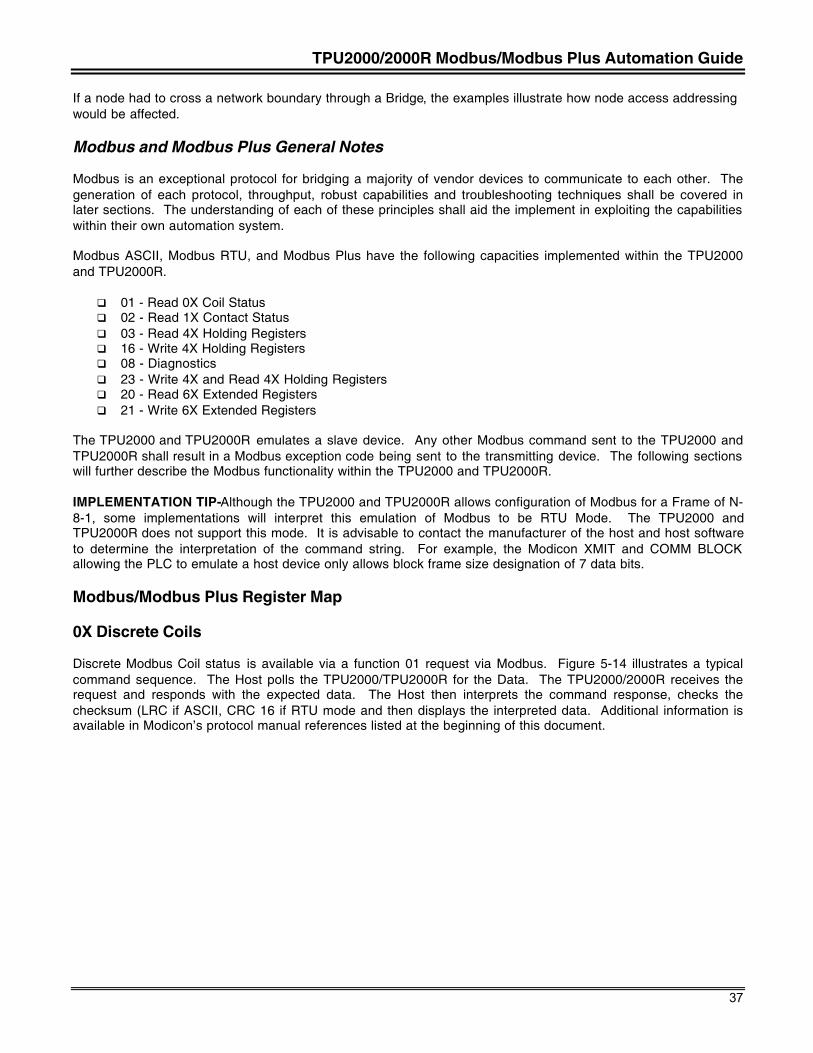
TPU2000/2000R Modbus/Modbus Plus Automation Guide
37
If a node had to cross a network boundary through a Bridge, the examples illustrate how node access addressingwould be affected.
Modbus and Modbus Plus General Notes
Modbus is an exceptional protocol for bridging a majority of vendor devices to communicate to each other. Thegeneration of each protocol, throughput, robust capabilities and troubleshooting techniques shall be covered inlater sections. The understanding of each of these principles shall aid the implement in exploiting the capabilitieswithin their own automation system.
Modbus ASCII, Modbus RTU, and Modbus Plus have the following capacities implemented within the TPU2000and TPU2000R.
q 01 - Read 0X Coil Statusq 02 - Read 1X Contact Statusq 03 - Read 4X Holding Registersq 16 - Write 4X Holding Registersq 08 - Diagnosticsq 23 - Write 4X and Read 4X Holding Registersq 20 - Read 6X Extended Registersq 21 - Write 6X Extended Registers
The TPU2000 and TPU2000R emulates a slave device. Any other Modbus command sent to the TPU2000 andTPU2000R shall result in a Modbus exception code being sent to the transmitting device. The following sectionswill further describe the Modbus functionality within the TPU2000 and TPU2000R.
IMPLEMENTATION TIP-Although the TPU2000 and TPU2000R allows configuration of Modbus for a Frame of N-8-1, some implementations will interpret this emulation of Modbus to be RTU Mode. The TPU2000 andTPU2000R does not support this mode. It is advisable to contact the manufacturer of the host and host softwareto determine the interpretation of the command string. For example, the Modicon XMIT and COMM BLOCKallowing the PLC to emulate a host device only allows block frame size designation of 7 data bits.
Modbus/Modbus Plus Register Map
0X Discrete Coils
Discrete Modbus Coil status is available via a function 01 request via Modbus. Figure 5-14 illustrates a typicalcommand sequence. The Host polls the TPU2000/TPU2000R for the Data. The TPU2000/2000R receives therequest and responds with the expected data. The Host then interprets the command response, checks thechecksum (LRC if ASCII, CRC 16 if RTU mode and then displays the interpreted data. Additional information isavailable in Modicon’s protocol manual references listed at the beginning of this document.
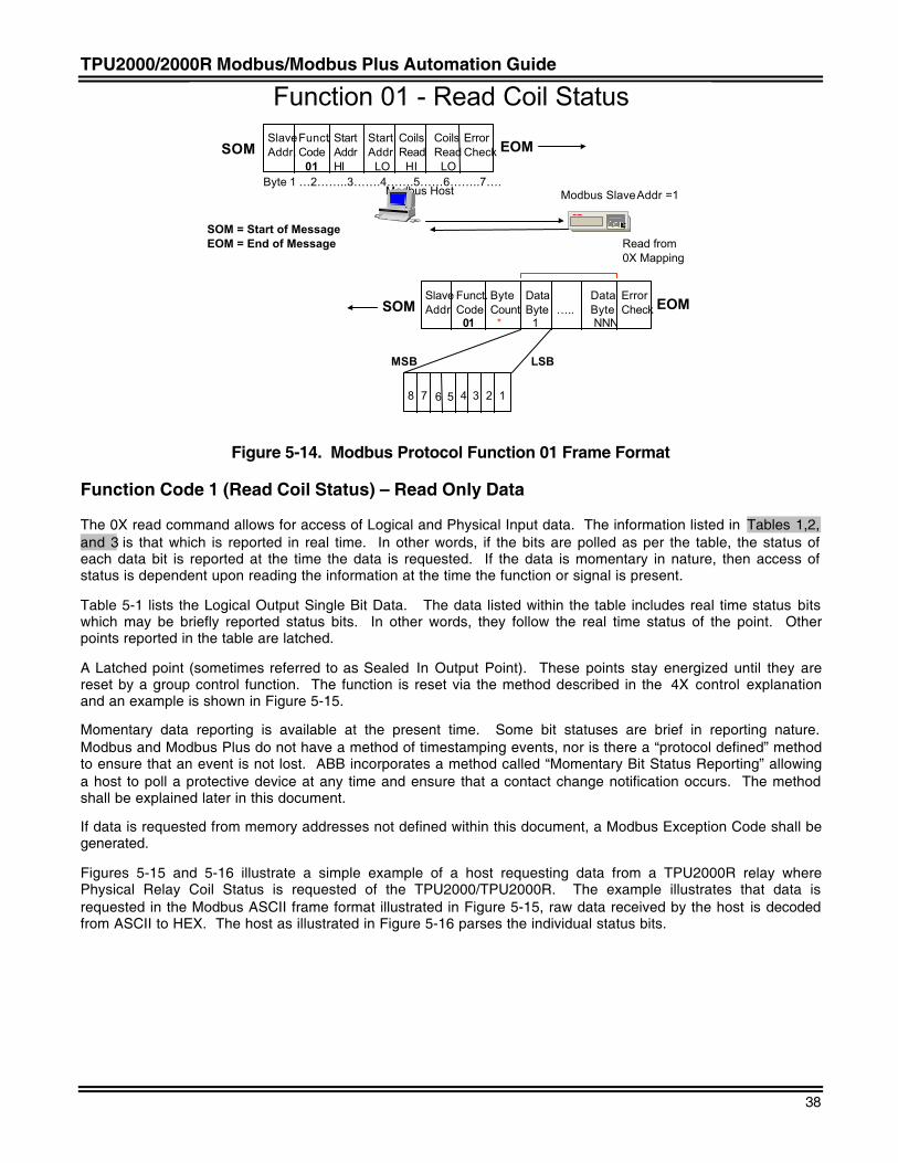
TPU2000/2000R Modbus/Modbus Plus Automation Guide
38
Function 01 - Read Coil Status
Modbus Host
EC
Modbus Slave Addr =1
Read from 0X Mapping
SlaveAddr.
Funct.Code 01
StartAddrHI
Start Addr LO
CoilsRead HI
CoilsRead LO
ErrorCheck EOMSOM
SlaveAddr.
Funct.Code 01
ByteCount *
DataByte 1
…..DataByte NNN
ErrorCheck EOMSOM
Byte 1 …2……..3…….4…….5……6……..7….
MSB LSB
8 7 6 5 4 3 2 1
SOM = Start of MessageEOM = End of Message
Figure 5-14. Modbus Protocol Function 01 Frame Format
Function Code 1 (Read Coil Status) – Read Only Data
The 0X read command allows for access of Logical and Physical Input data. The information listed in Tables 1,2,and 3 is that which is reported in real time. In other words, if the bits are polled as per the table, the status ofeach data bit is reported at the time the data is requested. If the data is momentary in nature, then access ofstatus is dependent upon reading the information at the time the function or signal is present.
Table 5-1 lists the Logical Output Single Bit Data. The data listed within the table includes real time status bitswhich may be briefly reported status bits. In other words, they follow the real time status of the point. Otherpoints reported in the table are latched.
A Latched point (sometimes referred to as Sealed In Output Point). These points stay energized until they arereset by a group control function. The function is reset via the method described in the 4X control explanationand an example is shown in Figure 5-15.
Momentary data reporting is available at the present time. Some bit statuses are brief in reporting nature.Modbus and Modbus Plus do not have a method of timestamping events, nor is there a “protocol defined” methodto ensure that an event is not lost. ABB incorporates a method called “Momentary Bit Status Reporting” allowinga host to poll a protective device at any time and ensure that a contact change notification occurs. The methodshall be explained later in this document.
If data is requested from memory addresses not defined within this document, a Modbus Exception Code shall begenerated.
Figures 5-15 and 5-16 illustrate a simple example of a host requesting data from a TPU2000R relay wherePhysical Relay Coil Status is requested of the TPU2000/TPU2000R. The example illustrates that data isrequested in the Modbus ASCII frame format illustrated in Figure 5-15, raw data received by the host is decodedfrom ASCII to HEX. The host as illustrated in Figure 5-16 parses the individual status bits.
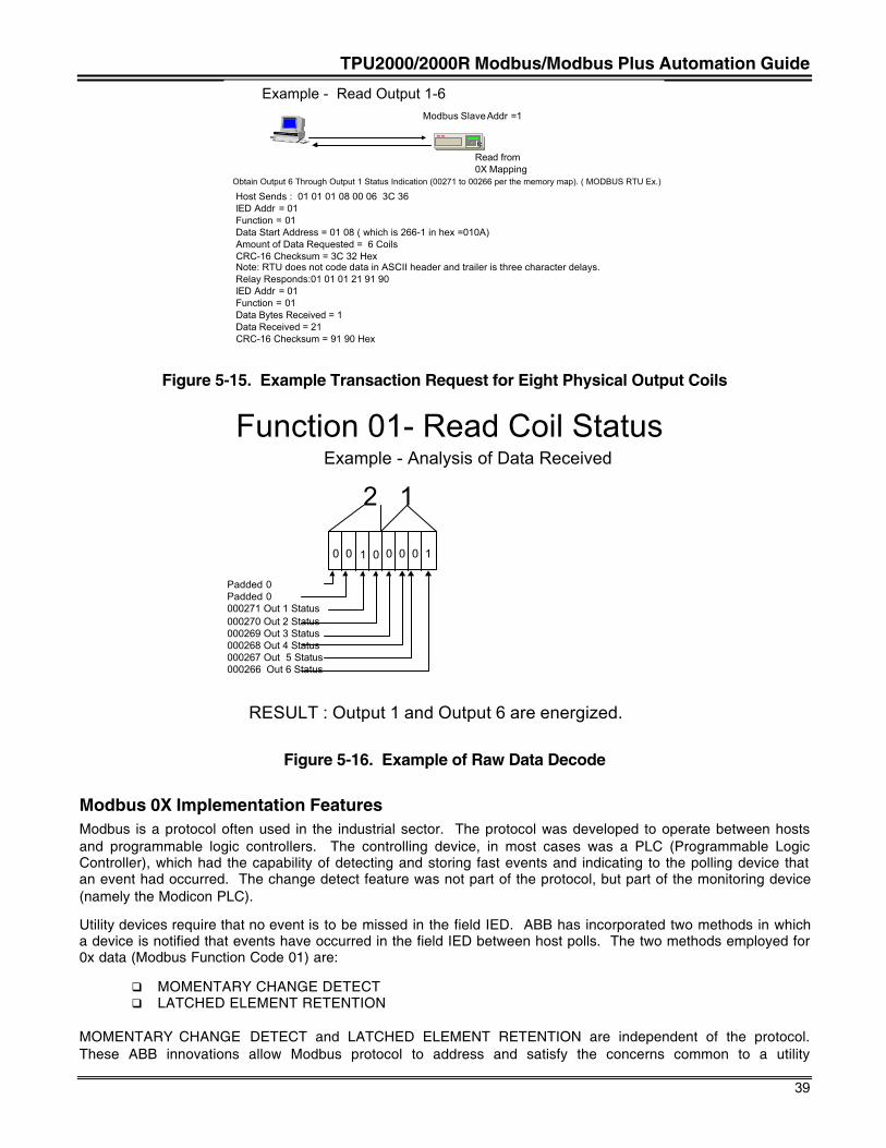
TPU2000/2000R Modbus/Modbus Plus Automation Guide
39
Example - Read Output 1-6
Obtain Output 6 Through Output 1 Status Indication (00271 to 00266 per the memory map). ( MODBUS RTU Ex.)
Host Sends : 01 01 01 08 00 06 3C 36IED Addr = 01Function = 01Data Start Address = 01 08 ( which is 266-1 in hex =010A)Amount of Data Requested = 6 CoilsCRC-16 Checksum = 3C 32 HexNote: RTU does not code data in ASCII header and trailer is three character delays.Relay Responds:01 01 01 21 91 90IED Addr = 01Function = 01Data Bytes Received = 1Data Received = 21CRC-16 Checksum = 91 90 Hex
Modbus Slave Addr =1
Read from 0X Mapping
EC
Figure 5-15. Example Transaction Request for Eight Physical Output Coils
Function 01- Read Coil Status
0 0 1 0 0 0 0 1
Example - Analysis of Data Received
2 1
Padded 0Padded 0000271 Out 1 Status000270 Out 2 Status000269 Out 3 Status000268 Out 4 Status000267 Out 5 Status000266 Out 6 Status
RESULT : Output 1 and Output 6 are energized.
Figure 5-16. Example of Raw Data Decode
Modbus 0X Implementation FeaturesModbus is a protocol often used in the industrial sector. The protocol was developed to operate between hostsand programmable logic controllers. The controlling device, in most cases was a PLC (Programmable LogicController), which had the capability of detecting and storing fast events and indicating to the polling device thatan event had occurred. The change detect feature was not part of the protocol, but part of the monitoring device(namely the Modicon PLC).
Utility devices require that no event is to be missed in the field IED. ABB has incorporated two methods in whicha device is notified that events have occurred in the field IED between host polls. The two methods employed for0x data (Modbus Function Code 01) are:
q MOMENTARY CHANGE DETECTq LATCHED ELEMENT RETENTION
MOMENTARY CHANGE DETECT and LATCHED ELEMENT RETENTION are independent of the protocol.These ABB innovations allow Modbus protocol to address and satisfy the concerns common to a utility
TPU2000/2000R Modbus/Modbus Plus Automation Guide
40
installation. The two functionality’s are those in excess of the real time status access that Modbus function code01 affords.
Momentary Change Detect status is incorporated using two bits to indicate present status and momentaryindication status. The odd bit is the status bit and the even bit is the momentary bit. The status bit indicates thepresent state of the element accessed. The momentary bit indicates element transitioning more than oncebetween IED reads. The momentary bit is set to a “1” if the element has transitioned more than once. The bit isreset upon a host access. Addresses 00513 through 01056 are allocated for momentary change bit detect statusdetection. NOTE: MOMENTARY BITS MUST BE READ IN PAIRS.
An example of momentary change detect is illustrated in Figure 5-17. Suppose a host device monitorsTPU2000R physical output bit 1. Figure 5-17 illustrates the physical output transitions of output 1. At each outputrising edge/falling edge transition, the status of the Modbus coil 0x addresses are listed. The dotted line arrowsindicate the poll received by the TPU2000R and the state of both the status bit and the momentary indication bit.Note that the even bit (momentary change detect) resets itself to a zero state after a host read.
EC OUTPUT 1 (ADDR 00270)
REAL TIME STATE00271 OUTPUT 1echo’s that of 01053 when read.
1
0
MOMENTARY STATE01053 STATUS OUTPUT 1
01054 MOMENTARY OUTPUT 1
TIME = 0
0 1 1 0 0 1 0 0 1 0 1 1
0 0 0 0 0 0 1 0 0 1 1 0
HOST READSDPU 2000R01053 = 101054 = 0
HOST READSDPU 2000R01053 = 001054 = 0
HOST READS HOST READSDPU 2000R DPU 2000R01053 = 0 01053 = 101054 = 1 01054 = 1
01054 RESETS AFTER HOST READ. OUTPUT 1 STATE TRANSITIONED MORE THAN ONCE BETWEEN HOST ACCESSES
Figure 5-17. Momentary Change Detect ExampleLatched Element Retention is a method by which when an element has transitions from a 0 (inactive), to a 1(active) status, the element is set to “1”. The element stays at a status of 1 until the operator executes a resetsequence. The reset of latched points may occur:
q The operator may depress the “SYSTEM RESET” pushbutton at the faceplate of the TPU2000Rq Depress the “C”, “E”, and “↑” (UP ARROW), keys simultaneously on the membrane keypad
(TPU2000R and TPU2000)q Initiate a supervisory bit reset sequence for the individual bits requiring reset. Reference Section 5 of
this guide for a detailed explanation of the reset procedure.
Figure 5-18 illustrates the operation of a latched bit sequence. The LATCHED elements are denoted with thesymbol (L) within the tables. Example latched elements are addresses 0050 through 0069 in Table 5-1 of thisdocument.
TPU2000/2000R Modbus/Modbus Plus Automation Guide
41
EC
REAL-TIME STATE00012 51 P-1
1
0
LATCHED STATE00062 51 P-1
TIME = 0
0 1 1 0 1 1
HOST READSDPU 2000RLATCHED STATUS= 1 WHEREAS THEFAULT HAS BEENCLEARED ANDREAL- TIME STATUS= 0 ( DEPENDING WHENPOLLED).
HOST OR OPERATOR PERFORMS DPU 2000R LATCH RESET SEQUENCE ON ELEMENT 51 P-1.
PHASE INSTANTANEOUSOVERCURRENT (51P)
1
0
Figure 5-18. Latched Element Status Example
Logical Output Block (Single Bit Data) – 108 Discrete Coils (99 Elements Defined 2Winding TPU, 176 Elements Defined for 3 Winding TPU)
Relay Element Status as described in Table 5-3. Additional coil status has been added in the latest version ofTPU2000/TPU2000R executive firmware. Consult the symbol keys in the table for revision level feature inclusion.
The status information reported in Table 5-3 is reported as real time status bits. Additional Latched or Seal In bitsare reported as status as illustrated in the following table.
Table 5-1. Logical Output Modbus Address Map Definition
RegisterAddress
Item Description
00513: DIFF STATUS Differential Trip Contact Energized (Status)00514: DIFF MOMENTARY Differential Trip Contact Energized (Momentary)00515: SELFCHECK ALARM
STATUSSelf Check Alarm Energized (Status)
00516: SELFCHECK ALARMMOMENTARY
Self Check Alarm Energized (Momentary)
00517: 87T STATUS Harmonic Restrained % Differential Trip Alarm Energized(Status)
00518: 87T MOMENTARY Harmonic Restrained % Differential Trip Alarm Energized(Momentary)
00519: 87H STATUS Unrestrained High Set Instantaneous Differential Trip AlarmEnergized (Status)
00520: 87H MOMENTARY Unrestrained High Set Instantaneous Differential Trip AlarmEnergized (Momentary)
00521: 2HROA STATUS 2nd Harmonic Restraint Alarm Energized (Status)00522: 2HROA MOMENTARY 2nd Harmonic Restraint Alarm Energized (Momentary)00523: 5HROA STATUS 5th Harmonic Restraint Alarm Energized (Status)00524: 5HROA MOMENTARY 5th Harmonic Restraint Alarm Energized (Momentary)00525: AHROA STATUS All Harmonics Restraint Alarm (2nd through 11th Harmonic)
Energized (Status)00526: AHROA MOMENTARY All Harmonics Restraint Alarm (2nd through 11th Harmonic)
Energized (Momentary)00527: TCFA STATUS Trip Circuit is Open Fail Alarm Energized (Status)00528: TCFA MOMENTARY Trip Circuit is Open Fail Alarm Energized (Momentary)00529: TFA STATUS Trip Fail Alarm Energized (Status)00530: TFA MOMENTARY Trip Fail Alarm Energized (Momentary)00531: 51P-1 STATUS Winding 1 Phase Time Overcurrent Alarm Energized (Status)00532: 51P-1 MOMENTARY Winding 1 Phase Time Overcurrent Alarm Energized
(Momentary)00533: 51P-2 STATUS Winding 2 Phase Time Overcurrent Alarm Energized (Status)
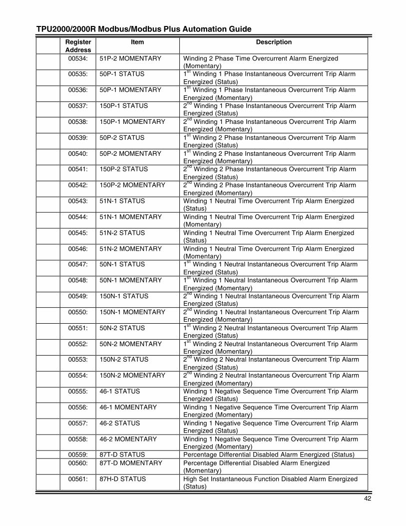
TPU2000/2000R Modbus/Modbus Plus Automation Guide
42
RegisterAddress
Item Description
00534: 51P-2 MOMENTARY Winding 2 Phase Time Overcurrent Alarm Energized(Momentary)
00535: 50P-1 STATUS 1st Winding 1 Phase Instantaneous Overcurrent Trip AlarmEnergized (Status)
00536: 50P-1 MOMENTARY 1st Winding 1 Phase Instantaneous Overcurrent Trip AlarmEnergized (Momentary)
00537: 150P-1 STATUS 2nd Winding 1 Phase Instantaneous Overcurrent Trip AlarmEnergized (Status)
00538: 150P-1 MOMENTARY 2nd Winding 1 Phase Instantaneous Overcurrent Trip AlarmEnergized (Momentary)
00539: 50P-2 STATUS 1st Winding 2 Phase Instantaneous Overcurrent Trip AlarmEnergized (Status)
00540: 50P-2 MOMENTARY 1st Winding 2 Phase Instantaneous Overcurrent Trip AlarmEnergized (Momentary)
00541: 150P-2 STATUS 2nd Winding 2 Phase Instantaneous Overcurrent Trip AlarmEnergized (Status)
00542: 150P-2 MOMENTARY 2nd Winding 2 Phase Instantaneous Overcurrent Trip AlarmEnergized (Momentary)
00543: 51N-1 STATUS Winding 1 Neutral Time Overcurrent Trip Alarm Energized(Status)
00544: 51N-1 MOMENTARY Winding 1 Neutral Time Overcurrent Trip Alarm Energized(Momentary)
00545: 51N-2 STATUS Winding 1 Neutral Time Overcurrent Trip Alarm Energized(Status)
00546: 51N-2 MOMENTARY Winding 1 Neutral Time Overcurrent Trip Alarm Energized(Momentary)
00547: 50N-1 STATUS 1st Winding 1 Neutral Instantaneous Overcurrent Trip AlarmEnergized (Status)
00548: 50N-1 MOMENTARY 1st Winding 1 Neutral Instantaneous Overcurrent Trip AlarmEnergized (Momentary)
00549: 150N-1 STATUS 2nd Winding 1 Neutral Instantaneous Overcurrent Trip AlarmEnergized (Status)
00550: 150N-1 MOMENTARY 2nd Winding 1 Neutral Instantaneous Overcurrent Trip AlarmEnergized (Momentary)
00551: 50N-2 STATUS 1st Winding 2 Neutral Instantaneous Overcurrent Trip AlarmEnergized (Status)
00552: 50N-2 MOMENTARY 1st Winding 2 Neutral Instantaneous Overcurrent Trip AlarmEnergized (Momentary)
00553: 150N-2 STATUS 2nd Winding 2 Neutral Instantaneous Overcurrent Trip AlarmEnergized (Status)
00554: 150N-2 MOMENTARY 2nd Winding 2 Neutral Instantaneous Overcurrent Trip AlarmEnergized (Momentary)
00555: 46-1 STATUS Winding 1 Negative Sequence Time Overcurrent Trip AlarmEnergized (Status)
00556: 46-1 MOMENTARY Winding 1 Negative Sequence Time Overcurrent Trip AlarmEnergized (Momentary)
00557: 46-2 STATUS Winding 1 Negative Sequence Time Overcurrent Trip AlarmEnergized (Status)
00558: 46-2 MOMENTARY Winding 1 Negative Sequence Time Overcurrent Trip AlarmEnergized (Momentary)
00559: 87T-D STATUS Percentage Differential Disabled Alarm Energized (Status)00560: 87T-D MOMENTARY Percentage Differential Disabled Alarm Energized
(Momentary)00561: 87H-D STATUS High Set Instantaneous Function Disabled Alarm Energized
(Status)
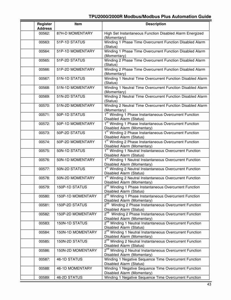
TPU2000/2000R Modbus/Modbus Plus Automation Guide
43
RegisterAddress
Item Description
00562: 87H-D MOMENTARY High Set Instantaneous Function Disabled Alarm Energized(Momentary)
00563: 51P-1D STATUS Winding 1 Phase Time Overcurrent Function Disabled Alarm(Status)
00564: 51P-1D MOMENTARY Winding 1 Phase Time Overcurrent Function Disabled Alarm(Momentary)
00565: 51P-2D STATUS Winding 2 Phase Time Overcurrent Function Disabled Alarm(Status)
00566: 51P-2D MOMENTARY Winding 2 Phase Time Overcurrent Function Disabled Alarm(Momentary)
00567: 51N-1D STATUS Winding 1 Neutral Time Overcurrent Function Disabled Alarm(Status)
00568: 51N-1D MOMENTARY Winding 1 Neutral Time Overcurrent Function Disabled Alarm(Momentary)
00569: 51N-2D STATUS Winding 2 Neutral Time Overcurrent Function Disabled Alarm(Status)
00570: 51N-2D MOMENTARY Winding 2 Neutral Time Overcurrent Function Disabled Alarm(Momentary)
00571: 50P-1D STATUS 1st Winding 1 Phase Instantaneous Overcurrent FunctionDisabled Alarm (Status)
00572: 50P-1D MOMENTARY 1st Winding 1 Phase Instantaneous Overcurrent FunctionDisabled Alarm (Momentary)
00573: 50P-2D STATUS 1st Winding 2 Phase Instantaneous Overcurrent FunctionDisabled Alarm (Status)
00574: 50P-2D MOMENTARY 1st Winding 2 Phase Instantaneous Overcurrent FunctionDisabled Alarm (Momentary)
00575: 50N-1D STATUS 1st Winding 1 Neutral Instantaneous Overcurrent FunctionDisabled Alarm (Status)
00576: 50N-1D MOMENTARY 1st Winding 1 Neutral Instantaneous Overcurrent FunctionDisabled Alarm (Momentary)
00577: 50N-2D STATUS 1st Winding 2 Neutral Instantaneous Overcurrent FunctionDisabled Alarm (Status)
00578: 50N-2D MOMENTARY 1st Winding 2 Neutral Instantaneous Overcurrent FunctionDisabled Alarm (Momentary)
00579: 150P-1D STATUS 2nd Winding 1 Phase Instantaneous Overcurrent FunctionDisabled Alarm (Status)
00580: 150P-1D MOMENTARY 2nd Winding 1 Phase Instantaneous Overcurrent FunctionDisabled Alarm (Momentary)
00581: 150P-2D STATUS 2nd Winding 2 Phase Instantaneous Overcurrent FunctionDisabled Alarm (Status)
00582: 150P-2D MOMENTARY 2nd Winding 2 Phase Instantaneous Overcurrent FunctionDisabled Alarm (Momentary)
00583: 150N-1D STATUS 2nd Winding 1 Neutral Instantaneous Overcurrent FunctionDisabled Alarm (Status)
00584: 150N-1D MOMENTARY 2nd Winding 1 Neutral Instantaneous Overcurrent FunctionDisabled Alarm (Momentary)
00585: 150N-2D STATUS 2nd Winding 2 Neutral Instantaneous Overcurrent FunctionDisabled Alarm (Status)
00586: 150N-2D MOMENTARY 2nd Winding 2 Neutral Instantaneous Overcurrent FunctionDisabled Alarm (Momentary)
00587: 46-1D STATUS Winding 1 Negative Sequence Time Overcurrent FunctionDisabled Alarm (Status)
00588: 46-1D MOMENTARY Winding 1 Negative Sequence Time Overcurrent FunctionDisabled Alarm (Momentary)
00589: 46-2D STATUS Winding 1 Negative Sequence Time Overcurrent Function
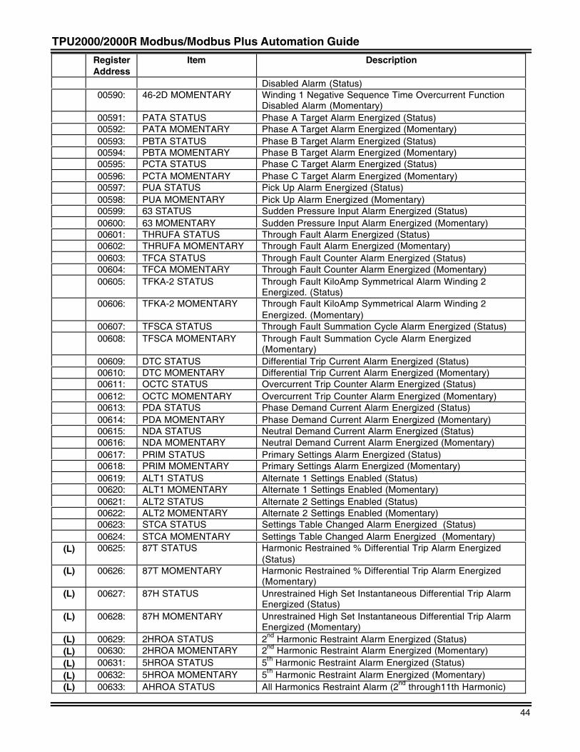
TPU2000/2000R Modbus/Modbus Plus Automation Guide
44
RegisterAddress
Item Description
Disabled Alarm (Status)00590: 46-2D MOMENTARY Winding 1 Negative Sequence Time Overcurrent Function
Disabled Alarm (Momentary)00591: PATA STATUS Phase A Target Alarm Energized (Status)00592: PATA MOMENTARY Phase A Target Alarm Energized (Momentary)00593: PBTA STATUS Phase B Target Alarm Energized (Status)00594: PBTA MOMENTARY Phase B Target Alarm Energized (Momentary)00595: PCTA STATUS Phase C Target Alarm Energized (Status)00596: PCTA MOMENTARY Phase C Target Alarm Energized (Momentary)00597: PUA STATUS Pick Up Alarm Energized (Status)00598: PUA MOMENTARY Pick Up Alarm Energized (Momentary)00599: 63 STATUS Sudden Pressure Input Alarm Energized (Status)00600: 63 MOMENTARY Sudden Pressure Input Alarm Energized (Momentary)00601: THRUFA STATUS Through Fault Alarm Energized (Status)00602: THRUFA MOMENTARY Through Fault Alarm Energized (Momentary)00603: TFCA STATUS Through Fault Counter Alarm Energized (Status)00604: TFCA MOMENTARY Through Fault Counter Alarm Energized (Momentary)00605: TFKA-2 STATUS Through Fault KiloAmp Symmetrical Alarm Winding 2
Energized. (Status)00606: TFKA-2 MOMENTARY Through Fault KiloAmp Symmetrical Alarm Winding 2
Energized. (Momentary)00607: TFSCA STATUS Through Fault Summation Cycle Alarm Energized (Status)00608: TFSCA MOMENTARY Through Fault Summation Cycle Alarm Energized
(Momentary)00609: DTC STATUS Differential Trip Current Alarm Energized (Status)00610: DTC MOMENTARY Differential Trip Current Alarm Energized (Momentary)00611: OCTC STATUS Overcurrent Trip Counter Alarm Energized (Status)00612: OCTC MOMENTARY Overcurrent Trip Counter Alarm Energized (Momentary)00613: PDA STATUS Phase Demand Current Alarm Energized (Status)00614: PDA MOMENTARY Phase Demand Current Alarm Energized (Momentary)00615: NDA STATUS Neutral Demand Current Alarm Energized (Status)00616: NDA MOMENTARY Neutral Demand Current Alarm Energized (Momentary)00617: PRIM STATUS Primary Settings Alarm Energized (Status)00618: PRIM MOMENTARY Primary Settings Alarm Energized (Momentary)00619: ALT1 STATUS Alternate 1 Settings Enabled (Status)00620: ALT1 MOMENTARY Alternate 1 Settings Enabled (Momentary)00621: ALT2 STATUS Alternate 2 Settings Enabled (Status)00622: ALT2 MOMENTARY Alternate 2 Settings Enabled (Momentary)00623: STCA STATUS Settings Table Changed Alarm Energized (Status)00624: STCA MOMENTARY Settings Table Changed Alarm Energized (Momentary)
(L) 00625: 87T STATUS Harmonic Restrained % Differential Trip Alarm Energized(Status)
(L) 00626: 87T MOMENTARY Harmonic Restrained % Differential Trip Alarm Energized(Momentary)
(L) 00627: 87H STATUS Unrestrained High Set Instantaneous Differential Trip AlarmEnergized (Status)
(L) 00628: 87H MOMENTARY Unrestrained High Set Instantaneous Differential Trip AlarmEnergized (Momentary)
(L) 00629: 2HROA STATUS 2nd Harmonic Restraint Alarm Energized (Status)(L) 00630: 2HROA MOMENTARY 2nd Harmonic Restraint Alarm Energized (Momentary)(L) 00631: 5HROA STATUS 5th Harmonic Restraint Alarm Energized (Status)(L) 00632: 5HROA MOMENTARY 5th Harmonic Restraint Alarm Energized (Momentary)(L) 00633: AHROA STATUS All Harmonics Restraint Alarm (2nd through11th Harmonic)
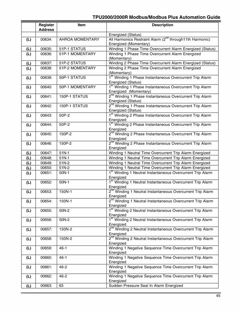
TPU2000/2000R Modbus/Modbus Plus Automation Guide
45
RegisterAddress
Item Description
Energized (Status)(L) 00634: AHROA MOMENTARY All Harmonics Restraint Alarm (2nd through11th Harmonic)
Energized (Momentary)(L) 00635: 51P-1 STATUS Winding 1 Phase Time Overcurrent Alarm Energized (Status)(L) 00636: 51P-1 MOMENTARY Winding 1 Phase Time Overcurrent Alarm Energized
(Momentary)(L) 00637: 51P-2 STATUS Winding 2 Phase Time Overcurrent Alarm Energized (Status)(L) 00638: 51P-2 MOMENTARY Winding 2 Phase Time Overcurrent Alarm Energized
(Momentary)(L) 00639: 50P-1 STATUS 1st Winding 1 Phase Instantaneous Overcurrent Trip Alarm
Energized (Status)(L) 00640: 50P-1 MOMENTARY 1st Winding 1 Phase Instantaneous Overcurrent Trip Alarm
Energized (Momentary)(L) 00641: 150P-1 STATUS 2nd Winding 1 Phase Instantaneous Overcurrent Trip Alarm
Energized (Status)(L) 00642: 150P-1 STATUS 2nd Winding 1 Phase Instantaneous Overcurrent Trip Alarm
Energized (Status)(L) 00643: 50P-2 1st Winding 2 Phase Instantaneous Overcurrent Trip Alarm
Energized(L) 00644: 50P-2 1st Winding 2 Phase Instantaneous Overcurrent Trip Alarm
Energized(L) 00645: 150P-2 2nd Winding 2 Phase Instantaneous Overcurrent Trip Alarm
Energized(L) 00646: 150P-2 2nd Winding 2 Phase Instantaneous Overcurrent Trip Alarm
Energized(L) 00647: 51N-1 Winding 1 Neutral Time Overcurrent Trip Alarm Energized(L) 00648: 51N-1 Winding 1 Neutral Time Overcurrent Trip Alarm Energized(L) 00649: 51N-2 Winding 1 Neutral Time Overcurrent Trip Alarm Energized(L) 00650: 51N-2 Winding 1 Neutral Time Overcurrent Trip Alarm Energized(L) 00651: 50N-1 1st Winding 1 Neutral Instantaneous Overcurrent Trip Alarm
Energized(L) 00652: 50N-1 1st Winding 1 Neutral Instantaneous Overcurrent Trip Alarm
Energized(L) 00653: 150N-1 2nd Winding 1 Neutral Instantaneous Overcurrent Trip Alarm
Energized(L) 00654: 150N-1 2nd Winding 1 Neutral Instantaneous Overcurrent Trip Alarm
Energized(L) 00655: 50N-2 1st Winding 2 Neutral Instantaneous Overcurrent Trip Alarm
Energized(L) 00656: 50N-2 1st Winding 2 Neutral Instantaneous Overcurrent Trip Alarm
Energized(L) 00657: 150N-2 2nd Winding 2 Neutral Instantaneous Overcurrent Trip Alarm
Energized(L) 00658: 150N-2 2nd Winding 2 Neutral Instantaneous Overcurrent Trip Alarm
Energized(L) 00659: 46-1 Winding 1 Negative Sequence Time Overcurrent Trip Alarm
Energized(L) 00660: 46-1 Winding 1 Negative Sequence Time Overcurrent Trip Alarm
Energized(L) 00661: 46-2 Winding 1 Negative Sequence Time Overcurrent Trip Alarm
Energized(L) 00662: 46-2 Winding 1 Negative Sequence Time Overcurrent Trip Alarm
Energized(L) 00663: 63 Sudden Pressure Seal In Alarm Energized
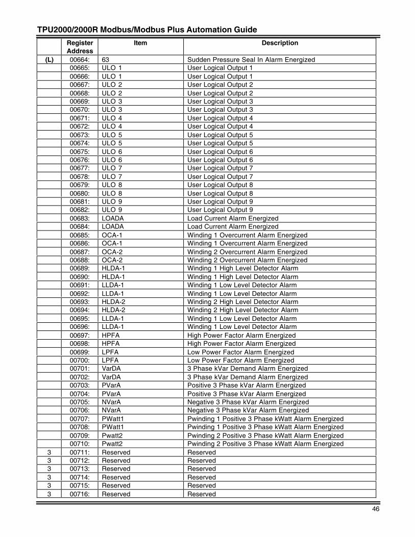
TPU2000/2000R Modbus/Modbus Plus Automation Guide
46
RegisterAddress
Item Description
(L) 00664: 63 Sudden Pressure Seal In Alarm Energized00665: ULO 1 User Logical Output 100666: ULO 1 User Logical Output 100667: ULO 2 User Logical Output 200668: ULO 2 User Logical Output 200669: ULO 3 User Logical Output 300670: ULO 3 User Logical Output 300671: ULO 4 User Logical Output 400672: ULO 4 User Logical Output 400673: ULO 5 User Logical Output 500674: ULO 5 User Logical Output 500675: ULO 6 User Logical Output 600676: ULO 6 User Logical Output 600677: ULO 7 User Logical Output 700678: ULO 7 User Logical Output 700679: ULO 8 User Logical Output 800680: ULO 8 User Logical Output 800681: ULO 9 User Logical Output 900682: ULO 9 User Logical Output 900683: LOADA Load Current Alarm Energized00684: LOADA Load Current Alarm Energized00685: OCA-1 Winding 1 Overcurrent Alarm Energized00686: OCA-1 Winding 1 Overcurrent Alarm Energized00687: OCA-2 Winding 2 Overcurrent Alarm Energized00688: OCA-2 Winding 2 Overcurrent Alarm Energized00689: HLDA-1 Winding 1 High Level Detector Alarm00690: HLDA-1 Winding 1 High Level Detector Alarm00691: LLDA-1 Winding 1 Low Level Detector Alarm00692: LLDA-1 Winding 1 Low Level Detector Alarm00693: HLDA-2 Winding 2 High Level Detector Alarm00694: HLDA-2 Winding 2 High Level Detector Alarm00695: LLDA-1 Winding 1 Low Level Detector Alarm00696: LLDA-1 Winding 1 Low Level Detector Alarm00697: HPFA High Power Factor Alarm Energized00698: HPFA High Power Factor Alarm Energized00699: LPFA Low Power Factor Alarm Energized00700: LPFA Low Power Factor Alarm Energized00701: VarDA 3 Phase kVar Demand Alarm Energized00702: VarDA 3 Phase kVar Demand Alarm Energized00703: PVarA Positive 3 Phase kVar Alarm Energized00704: PVarA Positive 3 Phase kVar Alarm Energized00705: NVarA Negative 3 Phase kVar Alarm Energized00706: NVarA Negative 3 Phase kVar Alarm Energized00707: PWatt1 Pwinding 1 Positive 3 Phase kWatt Alarm Energized00708: PWatt1 Pwinding 1 Positive 3 Phase kWatt Alarm Energized00709: Pwatt2 Pwinding 2 Positive 3 Phase kWatt Alarm Energized00710: Pwatt2 Pwinding 2 Positive 3 Phase kWatt Alarm Energized
3 00711: Reserved Reserved3 00712: Reserved Reserved3 00713: Reserved Reserved3 00714: Reserved Reserved3 00715: Reserved Reserved3 00716: Reserved Reserved
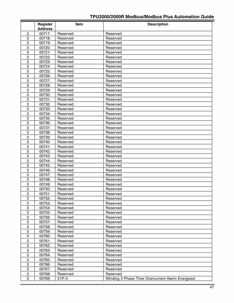
TPU2000/2000R Modbus/Modbus Plus Automation Guide
47
RegisterAddress
Item Description
3 00717: Reserved Reserved3 00718: Reserved Reserved3 00719: Reserved Reserved3 00720: Reserved Reserved3 00721: Reserved Reserved3 00722: Reserved Reserved3 00723: Reserved Reserved3 00724: Reserved Reserved3 00725: Reserved Reserved3 00726: Reserved Reserved3 00727: Reserved Reserved3 00728: Reserved Reserved3 00729: Reserved Reserved3 00730: Reserved Reserved3 00731: Reserved Reserved3 00732: Reserved Reserved3 00733: Reserved Reserved3 00734: Reserved Reserved3 00735: Reserved Reserved3 00736: Reserved Reserved3 00737: Reserved Reserved3 00738: Reserved Reserved3 00739: Reserved Reserved3 00740: Reserved Reserved3 00741: Reserved Reserved3 00742: Reserved Reserved3 00743: Reserved Reserved3 00744: Reserved Reserved3 00745: Reserved Reserved3 00746: Reserved Reserved3 00747: Reserved Reserved3 00748: Reserved Reserved3 00749: Reserved Reserved3 00750: Reserved Reserved3 00751: Reserved Reserved3 00752: Reserved Reserved3 00753: Reserved Reserved3 00754: Reserved Reserved3 00755: Reserved Reserved3 00756: Reserved Reserved3 00757: Reserved Reserved3 00758: Reserved Reserved3 00759: Reserved Reserved3 00760: Reserved Reserved3 00761: Reserved Reserved3 00762: Reserved Reserved3 00763: Reserved Reserved3 00764: Reserved Reserved3 00765: Reserved Reserved3 00766: Reserved Reserved3 00767: Reserved Reserved3 00768: Reserved Reserved3 00769: 51P-3 Winding 3 Phase Time Overcurrent Alarm Energized
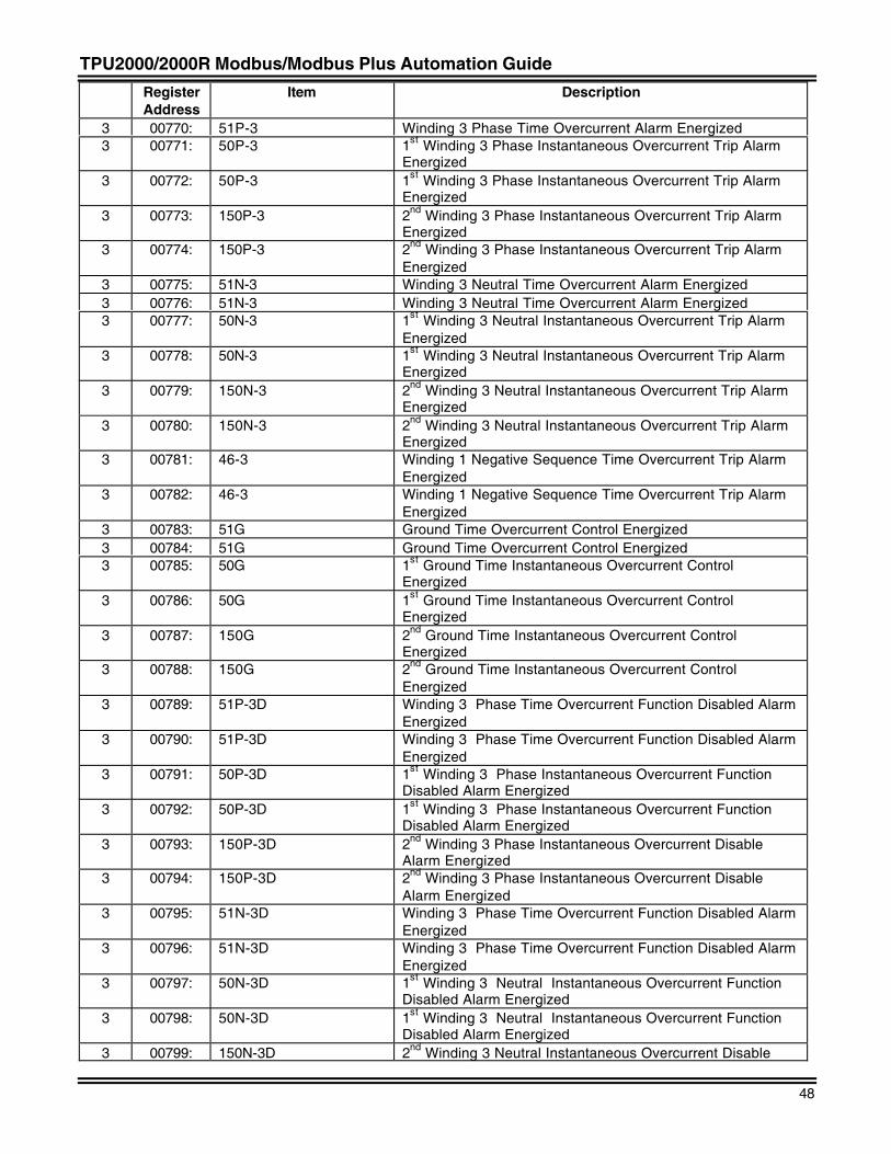
TPU2000/2000R Modbus/Modbus Plus Automation Guide
48
RegisterAddress
Item Description
3 00770: 51P-3 Winding 3 Phase Time Overcurrent Alarm Energized3 00771: 50P-3 1st Winding 3 Phase Instantaneous Overcurrent Trip Alarm
Energized3 00772: 50P-3 1st Winding 3 Phase Instantaneous Overcurrent Trip Alarm
Energized3 00773: 150P-3 2nd Winding 3 Phase Instantaneous Overcurrent Trip Alarm
Energized3 00774: 150P-3 2nd Winding 3 Phase Instantaneous Overcurrent Trip Alarm
Energized3 00775: 51N-3 Winding 3 Neutral Time Overcurrent Alarm Energized3 00776: 51N-3 Winding 3 Neutral Time Overcurrent Alarm Energized3 00777: 50N-3 1st Winding 3 Neutral Instantaneous Overcurrent Trip Alarm
Energized3 00778: 50N-3 1st Winding 3 Neutral Instantaneous Overcurrent Trip Alarm
Energized3 00779: 150N-3 2nd Winding 3 Neutral Instantaneous Overcurrent Trip Alarm
Energized3 00780: 150N-3 2nd Winding 3 Neutral Instantaneous Overcurrent Trip Alarm
Energized3 00781: 46-3 Winding 1 Negative Sequence Time Overcurrent Trip Alarm
Energized3 00782: 46-3 Winding 1 Negative Sequence Time Overcurrent Trip Alarm
Energized3 00783: 51G Ground Time Overcurrent Control Energized3 00784: 51G Ground Time Overcurrent Control Energized3 00785: 50G 1st Ground Time Instantaneous Overcurrent Control
Energized3 00786: 50G 1st Ground Time Instantaneous Overcurrent Control
Energized3 00787: 150G 2nd Ground Time Instantaneous Overcurrent Control
Energized3 00788: 150G 2nd Ground Time Instantaneous Overcurrent Control
Energized3 00789: 51P-3D Winding 3 Phase Time Overcurrent Function Disabled Alarm
Energized3 00790: 51P-3D Winding 3 Phase Time Overcurrent Function Disabled Alarm
Energized3 00791: 50P-3D 1st Winding 3 Phase Instantaneous Overcurrent Function
Disabled Alarm Energized3 00792: 50P-3D 1st Winding 3 Phase Instantaneous Overcurrent Function
Disabled Alarm Energized3 00793: 150P-3D 2nd Winding 3 Phase Instantaneous Overcurrent Disable
Alarm Energized3 00794: 150P-3D 2nd Winding 3 Phase Instantaneous Overcurrent Disable
Alarm Energized3 00795: 51N-3D Winding 3 Phase Time Overcurrent Function Disabled Alarm
Energized3 00796: 51N-3D Winding 3 Phase Time Overcurrent Function Disabled Alarm
Energized3 00797: 50N-3D 1st Winding 3 Neutral Instantaneous Overcurrent Function
Disabled Alarm Energized3 00798: 50N-3D 1st Winding 3 Neutral Instantaneous Overcurrent Function
Disabled Alarm Energized3 00799: 150N-3D 2nd Winding 3 Neutral Instantaneous Overcurrent Disable
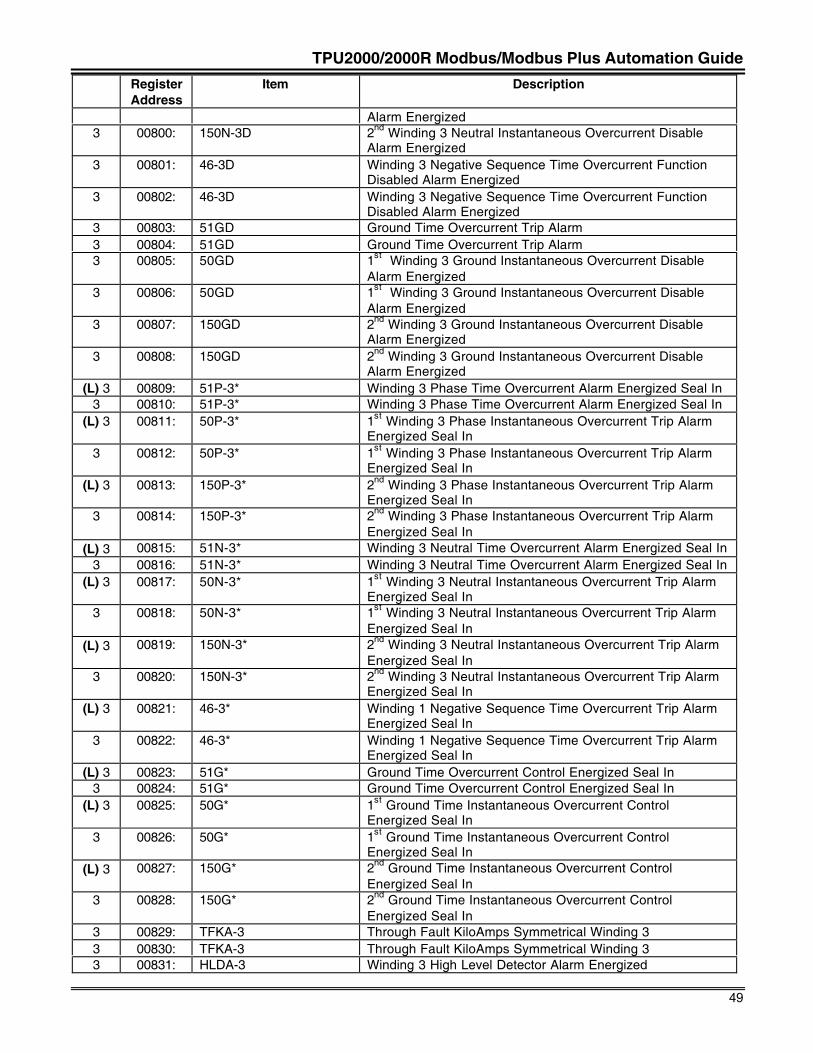
TPU2000/2000R Modbus/Modbus Plus Automation Guide
49
RegisterAddress
Item Description
Alarm Energized3 00800: 150N-3D 2nd Winding 3 Neutral Instantaneous Overcurrent Disable
Alarm Energized3 00801: 46-3D Winding 3 Negative Sequence Time Overcurrent Function
Disabled Alarm Energized3 00802: 46-3D Winding 3 Negative Sequence Time Overcurrent Function
Disabled Alarm Energized3 00803: 51GD Ground Time Overcurrent Trip Alarm3 00804: 51GD Ground Time Overcurrent Trip Alarm3 00805: 50GD 1st Winding 3 Ground Instantaneous Overcurrent Disable
Alarm Energized3 00806: 50GD 1st Winding 3 Ground Instantaneous Overcurrent Disable
Alarm Energized3 00807: 150GD 2nd Winding 3 Ground Instantaneous Overcurrent Disable
Alarm Energized3 00808: 150GD 2nd Winding 3 Ground Instantaneous Overcurrent Disable
Alarm Energized(L) 3 00809: 51P-3* Winding 3 Phase Time Overcurrent Alarm Energized Seal In
3 00810: 51P-3* Winding 3 Phase Time Overcurrent Alarm Energized Seal In(L) 3 00811: 50P-3* 1st Winding 3 Phase Instantaneous Overcurrent Trip Alarm
Energized Seal In3 00812: 50P-3* 1st Winding 3 Phase Instantaneous Overcurrent Trip Alarm
Energized Seal In(L) 3 00813: 150P-3* 2nd Winding 3 Phase Instantaneous Overcurrent Trip Alarm
Energized Seal In3 00814: 150P-3* 2nd Winding 3 Phase Instantaneous Overcurrent Trip Alarm
Energized Seal In(L) 3 00815: 51N-3* Winding 3 Neutral Time Overcurrent Alarm Energized Seal In
3 00816: 51N-3* Winding 3 Neutral Time Overcurrent Alarm Energized Seal In(L) 3 00817: 50N-3* 1st Winding 3 Neutral Instantaneous Overcurrent Trip Alarm
Energized Seal In3 00818: 50N-3* 1st Winding 3 Neutral Instantaneous Overcurrent Trip Alarm
Energized Seal In(L) 3 00819: 150N-3* 2nd Winding 3 Neutral Instantaneous Overcurrent Trip Alarm
Energized Seal In3 00820: 150N-3* 2nd Winding 3 Neutral Instantaneous Overcurrent Trip Alarm
Energized Seal In(L) 3 00821: 46-3* Winding 1 Negative Sequence Time Overcurrent Trip Alarm
Energized Seal In3 00822: 46-3* Winding 1 Negative Sequence Time Overcurrent Trip Alarm
Energized Seal In(L) 3 00823: 51G* Ground Time Overcurrent Control Energized Seal In
3 00824: 51G* Ground Time Overcurrent Control Energized Seal In(L) 3 00825: 50G* 1st Ground Time Instantaneous Overcurrent Control
Energized Seal In3 00826: 50G* 1st Ground Time Instantaneous Overcurrent Control
Energized Seal In(L) 3 00827: 150G* 2nd Ground Time Instantaneous Overcurrent Control
Energized Seal In3 00828: 150G* 2nd Ground Time Instantaneous Overcurrent Control
Energized Seal In3 00829: TFKA-3 Through Fault KiloAmps Symmetrical Winding 33 00830: TFKA-3 Through Fault KiloAmps Symmetrical Winding 33 00831: HLDA-3 Winding 3 High Level Detector Alarm Energized
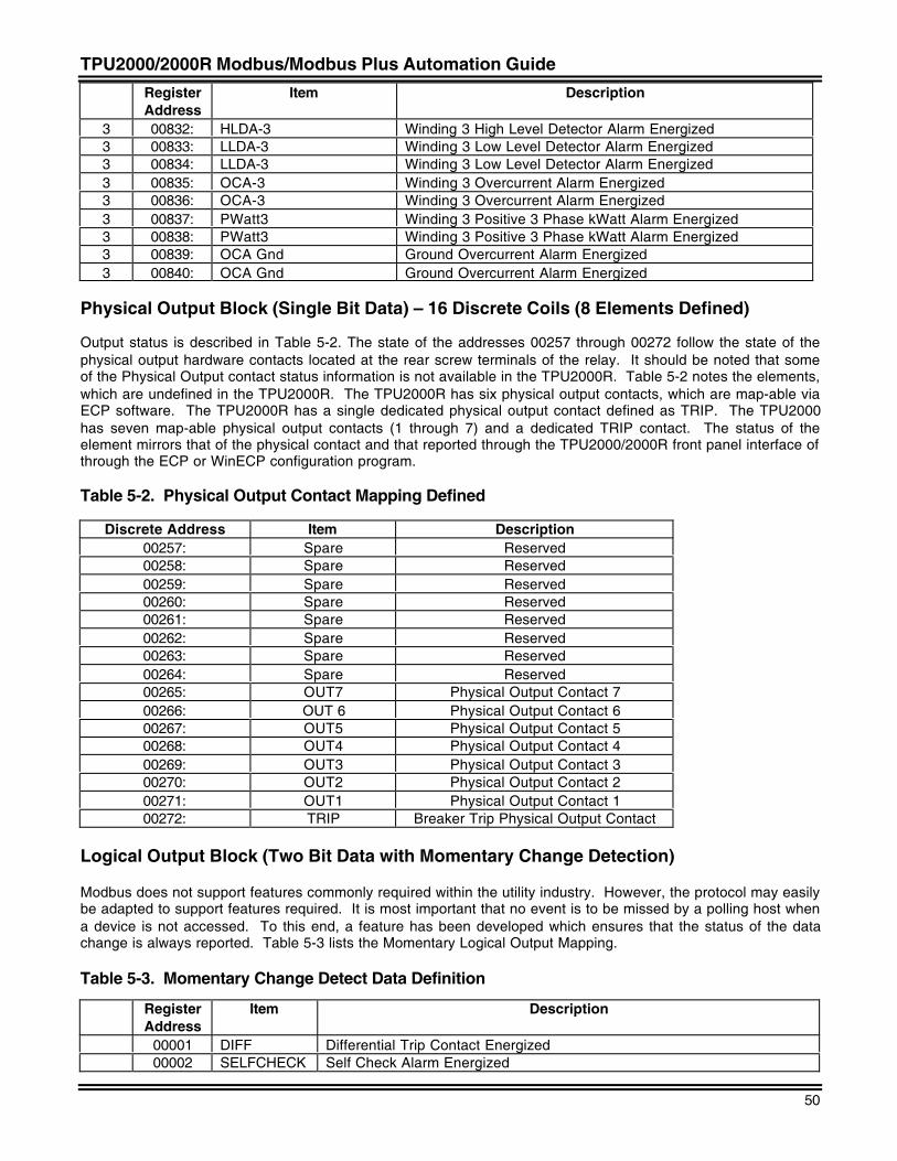
TPU2000/2000R Modbus/Modbus Plus Automation Guide
50
RegisterAddress
Item Description
3 00832: HLDA-3 Winding 3 High Level Detector Alarm Energized3 00833: LLDA-3 Winding 3 Low Level Detector Alarm Energized3 00834: LLDA-3 Winding 3 Low Level Detector Alarm Energized3 00835: OCA-3 Winding 3 Overcurrent Alarm Energized3 00836: OCA-3 Winding 3 Overcurrent Alarm Energized3 00837: PWatt3 Winding 3 Positive 3 Phase kWatt Alarm Energized3 00838: PWatt3 Winding 3 Positive 3 Phase kWatt Alarm Energized3 00839: OCA Gnd Ground Overcurrent Alarm Energized3 00840: OCA Gnd Ground Overcurrent Alarm Energized
Physical Output Block (Single Bit Data) – 16 Discrete Coils (8 Elements Defined)
Output status is described in Table 5-2. The state of the addresses 00257 through 00272 follow the state of thephysical output hardware contacts located at the rear screw terminals of the relay. It should be noted that someof the Physical Output contact status information is not available in the TPU2000R. Table 5-2 notes the elements,which are undefined in the TPU2000R. The TPU2000R has six physical output contacts, which are map-able viaECP software. The TPU2000R has a single dedicated physical output contact defined as TRIP. The TPU2000has seven map-able physical output contacts (1 through 7) and a dedicated TRIP contact. The status of theelement mirrors that of the physical contact and that reported through the TPU2000/2000R front panel interface ofthrough the ECP or WinECP configuration program.
Table 5-2. Physical Output Contact Mapping Defined
Discrete Address Item Description00257: Spare Reserved00258: Spare Reserved00259: Spare Reserved00260: Spare Reserved00261: Spare Reserved00262: Spare Reserved00263: Spare Reserved00264: Spare Reserved00265: OUT7 Physical Output Contact 700266: OUT 6 Physical Output Contact 600267: OUT5 Physical Output Contact 500268: OUT4 Physical Output Contact 400269: OUT3 Physical Output Contact 300270: OUT2 Physical Output Contact 200271: OUT1 Physical Output Contact 100272: TRIP Breaker Trip Physical Output Contact
Logical Output Block (Two Bit Data with Momentary Change Detection)
Modbus does not support features commonly required within the utility industry. However, the protocol may easilybe adapted to support features required. It is most important that no event is to be missed by a polling host whena device is not accessed. To this end, a feature has been developed which ensures that the status of the datachange is always reported. Table 5-3 lists the Momentary Logical Output Mapping.
Table 5-3. Momentary Change Detect Data Definition
RegisterAddress
Item Description
00001 DIFF Differential Trip Contact Energized00002 SELFCHECK Self Check Alarm Energized
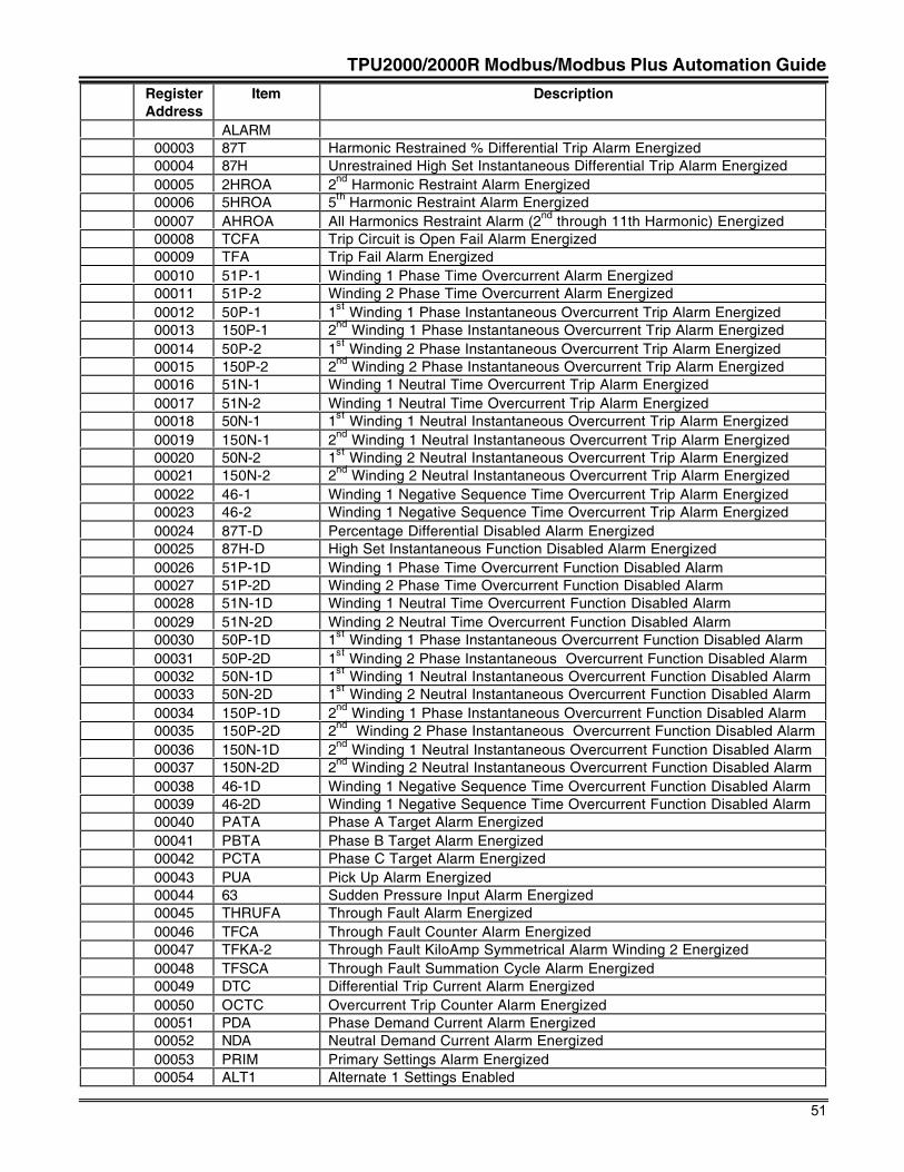
TPU2000/2000R Modbus/Modbus Plus Automation Guide
51
RegisterAddress
Item Description
ALARM00003 87T Harmonic Restrained % Differential Trip Alarm Energized00004 87H Unrestrained High Set Instantaneous Differential Trip Alarm Energized00005 2HROA 2nd Harmonic Restraint Alarm Energized00006 5HROA 5th Harmonic Restraint Alarm Energized00007 AHROA All Harmonics Restraint Alarm (2nd through 11th Harmonic) Energized00008 TCFA Trip Circuit is Open Fail Alarm Energized00009 TFA Trip Fail Alarm Energized00010 51P-1 Winding 1 Phase Time Overcurrent Alarm Energized00011 51P-2 Winding 2 Phase Time Overcurrent Alarm Energized00012 50P-1 1st Winding 1 Phase Instantaneous Overcurrent Trip Alarm Energized00013 150P-1 2nd Winding 1 Phase Instantaneous Overcurrent Trip Alarm Energized00014 50P-2 1st Winding 2 Phase Instantaneous Overcurrent Trip Alarm Energized00015 150P-2 2nd Winding 2 Phase Instantaneous Overcurrent Trip Alarm Energized00016 51N-1 Winding 1 Neutral Time Overcurrent Trip Alarm Energized00017 51N-2 Winding 1 Neutral Time Overcurrent Trip Alarm Energized00018 50N-1 1st Winding 1 Neutral Instantaneous Overcurrent Trip Alarm Energized00019 150N-1 2nd Winding 1 Neutral Instantaneous Overcurrent Trip Alarm Energized00020 50N-2 1st Winding 2 Neutral Instantaneous Overcurrent Trip Alarm Energized00021 150N-2 2nd Winding 2 Neutral Instantaneous Overcurrent Trip Alarm Energized00022 46-1 Winding 1 Negative Sequence Time Overcurrent Trip Alarm Energized00023 46-2 Winding 1 Negative Sequence Time Overcurrent Trip Alarm Energized00024 87T-D Percentage Differential Disabled Alarm Energized00025 87H-D High Set Instantaneous Function Disabled Alarm Energized00026 51P-1D Winding 1 Phase Time Overcurrent Function Disabled Alarm00027 51P-2D Winding 2 Phase Time Overcurrent Function Disabled Alarm00028 51N-1D Winding 1 Neutral Time Overcurrent Function Disabled Alarm00029 51N-2D Winding 2 Neutral Time Overcurrent Function Disabled Alarm00030 50P-1D 1st Winding 1 Phase Instantaneous Overcurrent Function Disabled Alarm00031 50P-2D 1st Winding 2 Phase Instantaneous Overcurrent Function Disabled Alarm00032 50N-1D 1st Winding 1 Neutral Instantaneous Overcurrent Function Disabled Alarm00033 50N-2D 1st Winding 2 Neutral Instantaneous Overcurrent Function Disabled Alarm00034 150P-1D 2nd Winding 1 Phase Instantaneous Overcurrent Function Disabled Alarm00035 150P-2D 2nd Winding 2 Phase Instantaneous Overcurrent Function Disabled Alarm00036 150N-1D 2nd Winding 1 Neutral Instantaneous Overcurrent Function Disabled Alarm00037 150N-2D 2nd Winding 2 Neutral Instantaneous Overcurrent Function Disabled Alarm00038 46-1D Winding 1 Negative Sequence Time Overcurrent Function Disabled Alarm00039 46-2D Winding 1 Negative Sequence Time Overcurrent Function Disabled Alarm00040 PATA Phase A Target Alarm Energized00041 PBTA Phase B Target Alarm Energized00042 PCTA Phase C Target Alarm Energized00043 PUA Pick Up Alarm Energized00044 63 Sudden Pressure Input Alarm Energized00045 THRUFA Through Fault Alarm Energized00046 TFCA Through Fault Counter Alarm Energized00047 TFKA-2 Through Fault KiloAmp Symmetrical Alarm Winding 2 Energized00048 TFSCA Through Fault Summation Cycle Alarm Energized00049 DTC Differential Trip Current Alarm Energized00050 OCTC Overcurrent Trip Counter Alarm Energized00051 PDA Phase Demand Current Alarm Energized00052 NDA Neutral Demand Current Alarm Energized00053 PRIM Primary Settings Alarm Energized00054 ALT1 Alternate 1 Settings Enabled
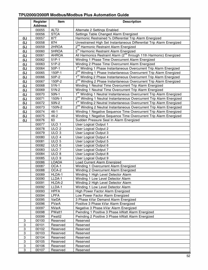
TPU2000/2000R Modbus/Modbus Plus Automation Guide
52
RegisterAddress
Item Description
00055 ALT2 Alternate 2 Settings Enabled00056 STCA Settings Table Changed Alarm Energized
(L) 00057 87T Harmonic Restrained % Differential Trip Alarm Energized(L) 00058 87H Unrestrained High Set Instantaneous Differential Trip Alarm Energized(L) 00059 2HROA 2nd Harmonic Restraint Alarm Energized(L) 00060 5HROA 5th Harmonic Restraint Alarm Energized(L) 00061 AHROA All Harmonics Restraint Alarm (2nd through 11th Harmonic) Energized(L) 00062 51P-1 Winding 1 Phase Time Overcurrent Alarm Energized(L) 00063 51P-2 Winding 2 Phase Time Overcurrent Alarm Energized(L) 00064 50P-1 1st Winding 1 Phase Instantaneous Overcurrent Trip Alarm Energized(L) 00065 150P-1 2nd Winding 1 Phase Instantaneous Overcurrent Trip Alarm Energized(L) 00066 50P-2 1st Winding 2 Phase Instantaneous Overcurrent Trip Alarm Energized(L) 00067 150P-2 2nd Winding 2 Phase Instantaneous Overcurrent Trip Alarm Energized(L) 00068 51N-1 Winding 1 Neutral Time Overcurrent Trip Alarm Energized(L) 00069 51N-2 Winding 1 Neutral Time Overcurrent Trip Alarm Energized(L) 00070 50N-1 1st Winding 1 Neutral Instantaneous Overcurrent Trip Alarm Energized(L) 00071 150N-1 2nd Winding 1 Neutral Instantaneous Overcurrent Trip Alarm Energized(L) 00072 50N-2 1st Winding 2 Neutral Instantaneous Overcurrent Trip Alarm Energized(L) 00073 150N-2 2nd Winding 2 Neutral Instantaneous Overcurrent Trip Alarm Energized(L) 00074 46-1 Winding 1 Negative Sequence Time Overcurrent Trip Alarm Energized(L) 00075 46-2 Winding 1 Negative Sequence Time Overcurrent Trip Alarm Energized(L) 00076 63 Sudden Pressure Seal In Alarm Energized
00077 ULO 1 User Logical Output 100078 ULO 2 User Logical Output 200079 ULO 3 User Logical Output 300080 ULO 4 User Logical Output 400081 ULO 5 User Logical Output 500082 ULO 6 User Logical Output 600083 ULO 7 User Logical Output 700084 ULO 8 User Logical Output 800085 ULO 9 User Logical Output 900086 LOADA Load Current Alarm Energized00087 OCA-1 Winding 1 Overcurrent Alarm Energized00088 OCA-2 Winding 2 Overcurrent Alarm Energized00089 HLDA-1 Winding 1 High Level Detector Alarm00090 LLDA-1 Winding 1 Low Level Detector Alarm00091 HLDA-2 Winding 2 High Level Detector Alarm00092 LLDA-1 Winding 1 Low Level Detector Alarm00093 HPFA High Power Factor Alarm Energized00094 LPFA Low Power Factor Alarm Energized00095 VarDA 3 Phase kVar Demand Alarm Energized00096 PVarA Positive 3 Phase kVar Alarm Energized00097 NVarA Negative 3 Phase kVar Alarm Energized00098 PWatt1 Pwinding 1 Positive 3 Phase kWatt Alarm Energized00099 Pwatt2 Pwinding 2 Positive 3 Phase kWatt Alarm Energized
3 00100 Reserved Reserved3 00101 Reserved Reserved3 00102 Reserved Reserved3 00103 Reserved Reserved3 00104 Reserved Reserved3 00105 Reserved Reserved3 00106 Reserved Reserved3 00107 Reserved Reserved
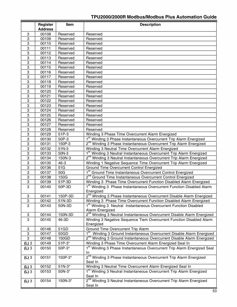
TPU2000/2000R Modbus/Modbus Plus Automation Guide
53
RegisterAddress
Item Description
3 00108 Reserved Reserved3 00109 Reserved Reserved3 00110 Reserved Reserved3 00111 Reserved Reserved3 00112 Reserved Reserved3 00113 Reserved Reserved3 00114 Reserved Reserved3 00115 Reserved Reserved3 00116 Reserved Reserved3 00117 Reserved Reserved3 00118 Reserved Reserved3 00119 Reserved Reserved3 00120 Reserved Reserved3 00121 Reserved Reserved3 00122 Reserved Reserved3 00123 Reserved Reserved3 00124 Reserved Reserved3 00125 Reserved Reserved3 00126 Reserved Reserved3 00127 Reserved Reserved3 00128 Reserved Reserved3 00129 51P-3 Winding 3 Phase Time Overcurrent Alarm Energized3 00130 50P-3 1st Winding 3 Phase Instantaneous Overcurrent Trip Alarm Energized3 00131 150P-3 2nd Winding 3 Phase Instantaneous Overcurrent Trip Alarm Energized3 00132 51N-3 Winding 3 Neutral Time Overcurrent Alarm Energized3 00133 50N-3 1st Winding 3 Neutral Instantaneous Overcurrent Trip Alarm Energized3 00134 150N-3 2nd Winding 3 Neutral Instantaneous Overcurrent Trip Alarm Energized3 00135 46-3 Winding 1 Negative Sequence Time Overcurrent Trip Alarm Energized3 00136 51G Ground Time Overcurrent Control Energized3 00137 50G 1st Ground Time Instantaneous Overcurrent Control Energized3 00138 150G 2nd Ground Time Instantaneous Overcurrent Control Energized3 00139 51P-3D Winding 3 Phase Time Overcurrent Function Disabled Alarm Energized3 00140 50P-3D 1st Winding 3 Phase Instantaneous Overcurrent Function Disabled Alarm
Energized3 00141 150P-3D 2nd Winding 3 Phase Instantaneous Overcurrent Disable Alarm Energized3 00142 51N-3D Winding 3 Phase Time Overcurrent Function Disabled Alarm Energized3 00143 50N-3D 1st Winding 3 Neutral Instantaneous Overcurrent Function Disabled
Alarm Energized3 00144 150N-3D 2nd Winding 3 Neutral Instantaneous Overcurrent Disable Alarm Energized3 00145 46-3D Winding 3 Negative Sequence Tiem Overcurrent Function Disabled Alarm
Energized3 00146 51GD Ground Time Overcurrent Trip Alarm3 00147 50GD 1st Winding 3 Ground Instantaneous Overcurrent Disable Alarm Energized3 00148 150GD 2nd Winding 3 Ground Instantaneous Overcurrent Disable Alarm Energized
(L) 3 00149 51P-3* Winding 3 Phase Time Overcurrent Alarm Energized Seal In(L) 3 00150 50P-3* 1st Winding 3 Phase Instantaneous Overcurrent Trip Alarm Energized Seal
In(L) 3 00151 150P-3* 2nd Winding 3 Phase Instantaneous Overcurrent Trip Alarm Energized
Seal In(L) 3 00152 51N-3* Winding 3 Neutral Time Overcurrent Alarm Energized Seal In(L) 3 00153 50N-3* 1st Winding 3 Neutral Instantaneous Overcurrent Trip Alarm Energized
Seal In(L) 3 00154 150N-3* 2nd Winding 3 Neutral Instantaneous Overcurrent Trip Alarm Energized
Seal In
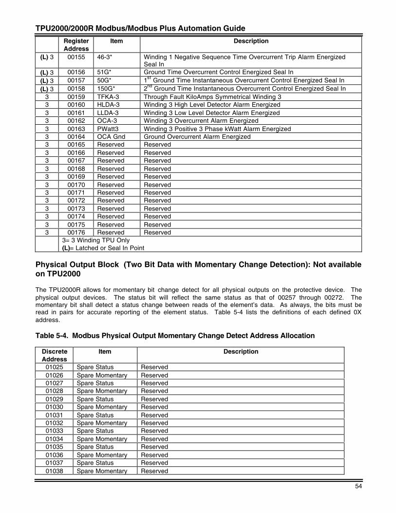
TPU2000/2000R Modbus/Modbus Plus Automation Guide
54
RegisterAddress
Item Description
(L) 3 00155 46-3* Winding 1 Negative Sequence Time Overcurrent Trip Alarm EnergizedSeal In
(L) 3 00156 51G* Ground Time Overcurrent Control Energized Seal In(L) 3 00157 50G* 1st Ground Time Instantaneous Overcurrent Control Energized Seal In(L) 3 00158 150G* 2nd Ground Time Instantaneous Overcurrent Control Energized Seal In
3 00159 TFKA-3 Through Fault KiloAmps Symmetrical Winding 33 00160 HLDA-3 Winding 3 High Level Detector Alarm Energized3 00161 LLDA-3 Winding 3 Low Level Detector Alarm Energized3 00162 OCA-3 Winding 3 Overcurrent Alarm Energized3 00163 PWatt3 Winding 3 Positive 3 Phase kWatt Alarm Energized3 00164 OCA Gnd Ground Overcurrent Alarm Energized3 00165 Reserved Reserved3 00166 Reserved Reserved3 00167 Reserved Reserved3 00168 Reserved Reserved3 00169 Reserved Reserved3 00170 Reserved Reserved3 00171 Reserved Reserved3 00172 Reserved Reserved3 00173 Reserved Reserved3 00174 Reserved Reserved3 00175 Reserved Reserved3 00176 Reserved Reserved
3= 3 Winding TPU Only(L)= Latched or Seal In Point
Physical Output Block (Two Bit Data with Momentary Change Detection): Not availableon TPU2000
The TPU2000R allows for momentary bit change detect for all physical outputs on the protective device. Thephysical output devices. The status bit will reflect the same status as that of 00257 through 00272. Themomentary bit shall detect a status change between reads of the element’s data. As always, the bits must beread in pairs for accurate reporting of the element status. Table 5-4 lists the definitions of each defined 0Xaddress.
Table 5-4. Modbus Physical Output Momentary Change Detect Address Allocation
DiscreteAddress
Item Description
01025 Spare Status Reserved01026 Spare Momentary Reserved01027 Spare Status Reserved01028 Spare Momentary Reserved01029 Spare Status Reserved01030 Spare Momentary Reserved01031 Spare Status Reserved01032 Spare Momentary Reserved01033 Spare Status Reserved01034 Spare Momentary Reserved01035 Spare Status Reserved01036 Spare Momentary Reserved01037 Spare Status Reserved01038 Spare Momentary Reserved
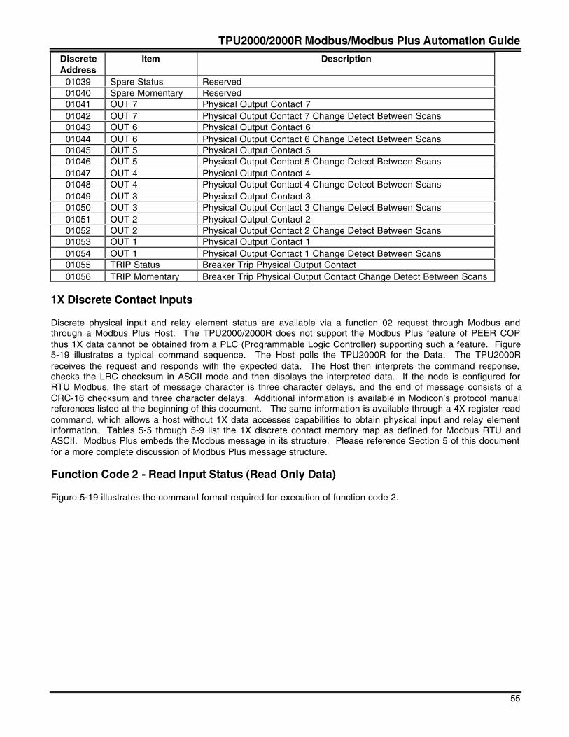
TPU2000/2000R Modbus/Modbus Plus Automation Guide
55
DiscreteAddress
Item Description
01039 Spare Status Reserved01040 Spare Momentary Reserved01041 OUT 7 Physical Output Contact 701042 OUT 7 Physical Output Contact 7 Change Detect Between Scans01043 OUT 6 Physical Output Contact 601044 OUT 6 Physical Output Contact 6 Change Detect Between Scans01045 OUT 5 Physical Output Contact 501046 OUT 5 Physical Output Contact 5 Change Detect Between Scans01047 OUT 4 Physical Output Contact 401048 OUT 4 Physical Output Contact 4 Change Detect Between Scans01049 OUT 3 Physical Output Contact 301050 OUT 3 Physical Output Contact 3 Change Detect Between Scans01051 OUT 2 Physical Output Contact 201052 OUT 2 Physical Output Contact 2 Change Detect Between Scans01053 OUT 1 Physical Output Contact 101054 OUT 1 Physical Output Contact 1 Change Detect Between Scans01055 TRIP Status Breaker Trip Physical Output Contact01056 TRIP Momentary Breaker Trip Physical Output Contact Change Detect Between Scans
1X Discrete Contact Inputs
Discrete physical input and relay element status are available via a function 02 request through Modbus andthrough a Modbus Plus Host. The TPU2000/2000R does not support the Modbus Plus feature of PEER COPthus 1X data cannot be obtained from a PLC (Programmable Logic Controller) supporting such a feature. Figure5-19 illustrates a typical command sequence. The Host polls the TPU2000R for the Data. The TPU2000Rreceives the request and responds with the expected data. The Host then interprets the command response,checks the LRC checksum in ASCII mode and then displays the interpreted data. If the node is configured forRTU Modbus, the start of message character is three character delays, and the end of message consists of aCRC-16 checksum and three character delays. Additional information is available in Modicon’s protocol manualreferences listed at the beginning of this document. The same information is available through a 4X register readcommand, which allows a host without 1X data accesses capabilities to obtain physical input and relay elementinformation. Tables 5-5 through 5-9 list the 1X discrete contact memory map as defined for Modbus RTU andASCII. Modbus Plus embeds the Modbus message in its structure. Please reference Section 5 of this documentfor a more complete discussion of Modbus Plus message structure.
Function Code 2 - Read Input Status (Read Only Data)
Figure 5-19 illustrates the command format required for execution of function code 2.
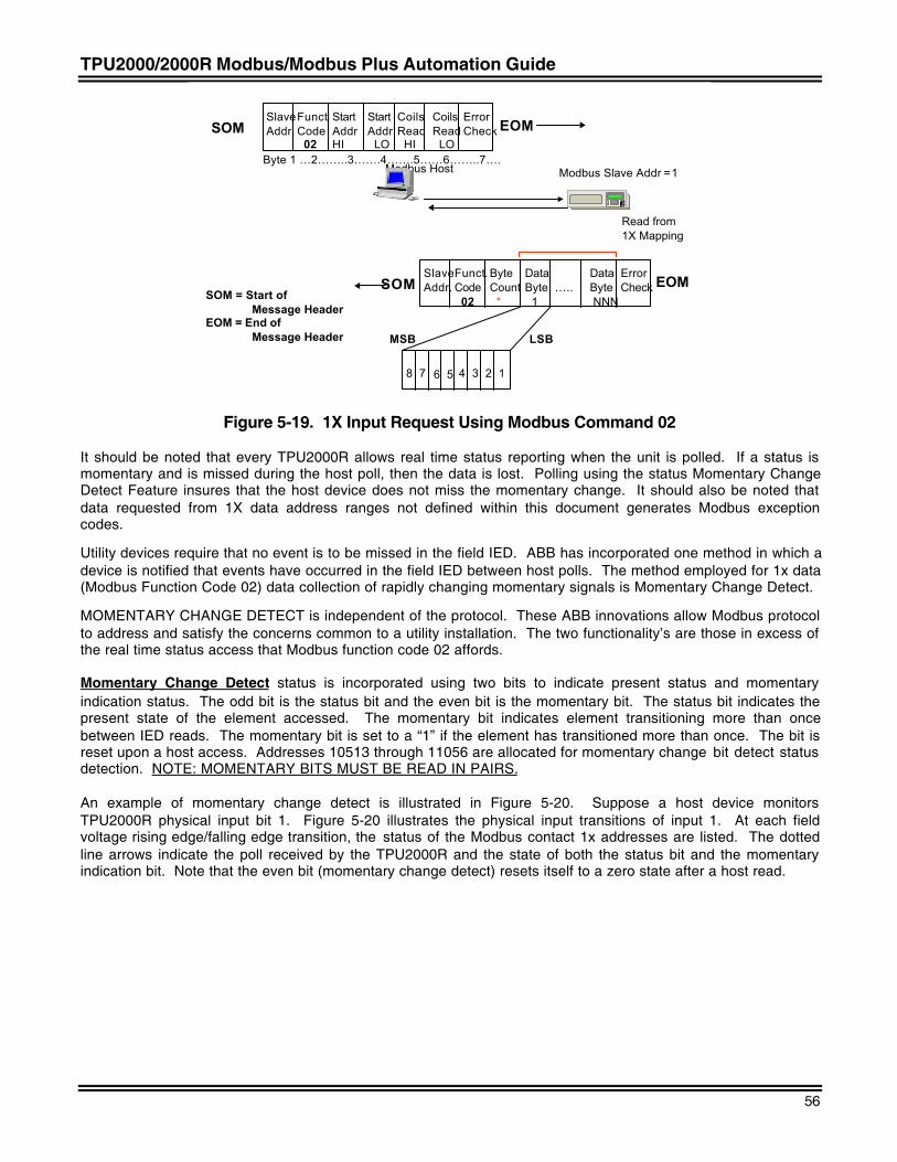
TPU2000/2000R Modbus/Modbus Plus Automation Guide
56
Modbus Host Modbus Slave Addr =1
Read from 1X Mapping
SlaveAddr.
Funct.Code 02
StartAddrHI
Start Addr LO
CoilsRead HI
CoilsRead LO
ErrorCheck EOMSOM
SlaveAddr.
Funct.Code 02
ByteCount *
DataByte 1
…..DataByte NNN
ErrorCheck EOMSOM
Byte 1 …2……..3…….4…….5……6……..7….
MSB LSB
8 7 6 5 4 3 2 1
SOM = Start of Message HeaderEOM = End of Message Header
EC
Figure 5-19. 1X Input Request Using Modbus Command 02
It should be noted that every TPU2000R allows real time status reporting when the unit is polled. If a status ismomentary and is missed during the host poll, then the data is lost. Polling using the status Momentary ChangeDetect Feature insures that the host device does not miss the momentary change. It should also be noted thatdata requested from 1X data address ranges not defined within this document generates Modbus exceptioncodes.
Utility devices require that no event is to be missed in the field IED. ABB has incorporated one method in which adevice is notified that events have occurred in the field IED between host polls. The method employed for 1x data(Modbus Function Code 02) data collection of rapidly changing momentary signals is Momentary Change Detect.
MOMENTARY CHANGE DETECT is independent of the protocol. These ABB innovations allow Modbus protocolto address and satisfy the concerns common to a utility installation. The two functionality’s are those in excess ofthe real time status access that Modbus function code 02 affords.
Momentary Change Detect status is incorporated using two bits to indicate present status and momentaryindication status. The odd bit is the status bit and the even bit is the momentary bit. The status bit indicates thepresent state of the element accessed. The momentary bit indicates element transitioning more than oncebetween IED reads. The momentary bit is set to a “1” if the element has transitioned more than once. The bit isreset upon a host access. Addresses 10513 through 11056 are allocated for momentary change bit detect statusdetection. NOTE: MOMENTARY BITS MUST BE READ IN PAIRS.
An example of momentary change detect is illustrated in Figure 5-20. Suppose a host device monitorsTPU2000R physical input bit 1. Figure 5-20 illustrates the physical input transitions of input 1. At each fieldvoltage rising edge/falling edge transition, the status of the Modbus contact 1x addresses are listed. The dottedline arrows indicate the poll received by the TPU2000R and the state of both the status bit and the momentaryindication bit. Note that the even bit (momentary change detect) resets itself to a zero state after a host read.
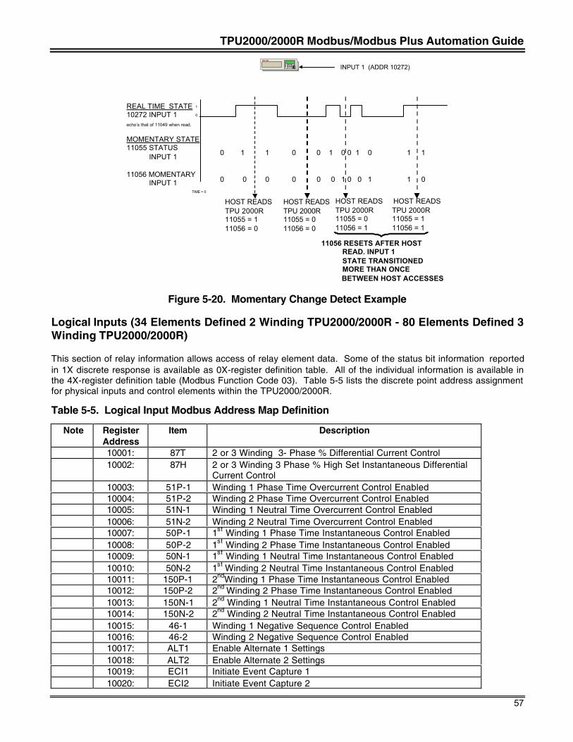
TPU2000/2000R Modbus/Modbus Plus Automation Guide
57
EC INPUT 1 (ADDR 10272)
REAL TIME STATE10272 INPUT 1echo’s that of 11049 when read.
1
0
MOMENTARY STATE11055 STATUS INPUT 1
11056 MOMENTARY INPUT 1
TIME = 0
0 1 1 0 0 1 0 0 1 0 1 1
0 0 0 0 0 0 1 0 0 1 1 0
HOST READSTPU 2000R11055 = 111056 = 0
HOST READSTPU 2000R11055 = 011056 = 0
HOST READS HOST READSTPU 2000R TPU 2000R11055 = 0 11055 = 111056 = 1 11056 = 1
11056 RESETS AFTER HOST READ. INPUT 1 STATE TRANSITIONED MORE THAN ONCE BETWEEN HOST ACCESSES
Figure 5-20. Momentary Change Detect Example
Logical Inputs (34 Elements Defined 2 Winding TPU2000/2000R - 80 Elements Defined 3Winding TPU2000/2000R)
This section of relay information allows access of relay element data. Some of the status bit information reportedin 1X discrete response is available as 0X-register definition table. All of the individual information is available inthe 4X-register definition table (Modbus Function Code 03). Table 5-5 lists the discrete point address assignmentfor physical inputs and control elements within the TPU2000/2000R.
Table 5-5. Logical Input Modbus Address Map Definition
Note RegisterAddress
Item Description
10001: 87T 2 or 3 Winding 3- Phase % Differential Current Control10002: 87H 2 or 3 Winding 3 Phase % High Set Instantaneous Differential
Current Control10003: 51P-1 Winding 1 Phase Time Overcurrent Control Enabled10004: 51P-2 Winding 2 Phase Time Overcurrent Control Enabled10005: 51N-1 Winding 1 Neutral Time Overcurrent Control Enabled10006: 51N-2 Winding 2 Neutral Time Overcurrent Control Enabled10007: 50P-1 1st Winding 1 Phase Time Instantaneous Control Enabled10008: 50P-2 1st Winding 2 Phase Time Instantaneous Control Enabled10009: 50N-1 1st Winding 1 Neutral Time Instantaneous Control Enabled10010: 50N-2 1st Winding 2 Neutral Time Instantaneous Control Enabled10011: 150P-1 2ndWinding 1 Phase Time Instantaneous Control Enabled10012: 150P-2 2nd Winding 2 Phase Time Instantaneous Control Enabled10013: 150N-1 2nd Winding 1 Neutral Time Instantaneous Control Enabled10014: 150N-2 2nd Winding 2 Neutral Time Instantaneous Control Enabled10015: 46-1 Winding 1 Negative Sequence Control Enabled10016: 46-2 Winding 2 Negative Sequence Control Enabled10017: ALT1 Enable Alternate 1 Settings10018: ALT2 Enable Alternate 2 Settings10019: ECI1 Initiate Event Capture 110020: ECI2 Initiate Event Capture 2
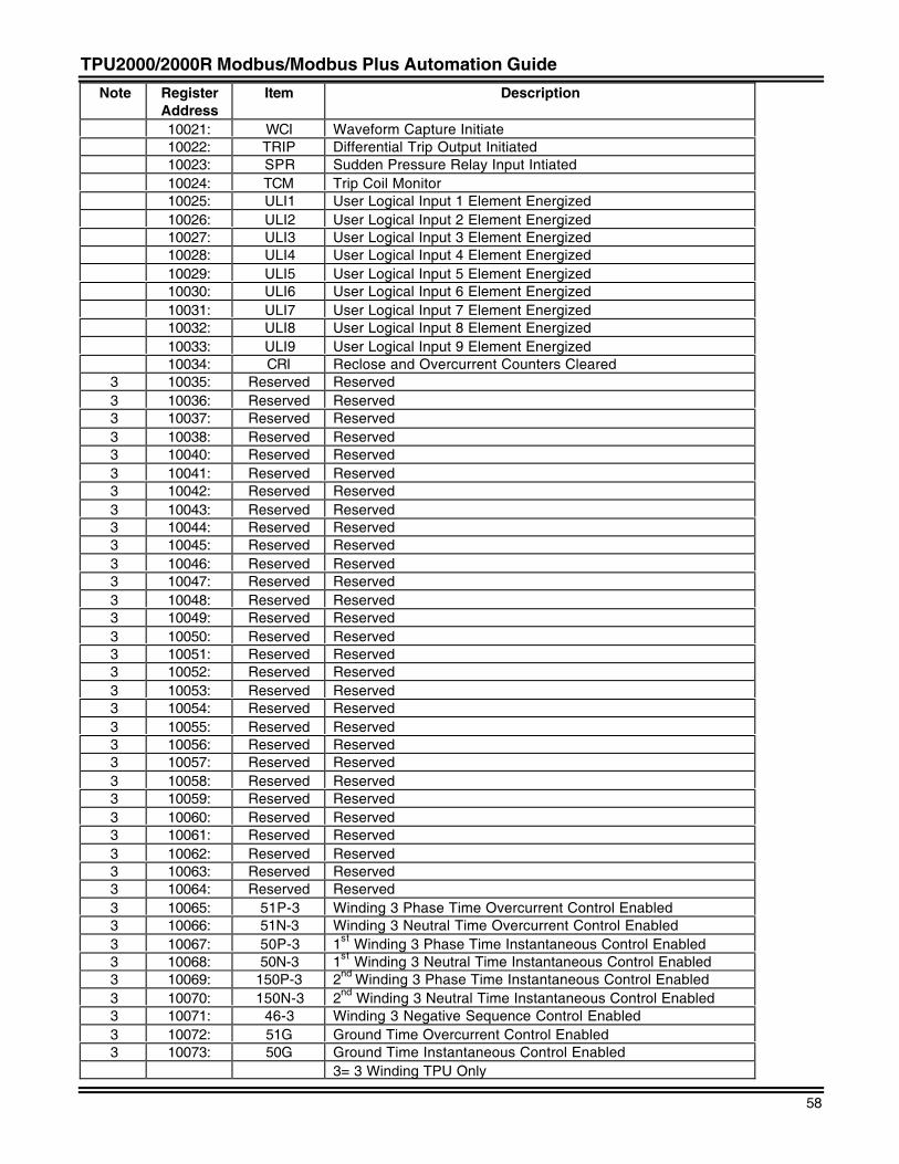
TPU2000/2000R Modbus/Modbus Plus Automation Guide
58
Note RegisterAddress
Item Description
10021: WCI Waveform Capture Initiate10022: TRIP Differential Trip Output Initiated10023: SPR Sudden Pressure Relay Input Intiated10024: TCM Trip Coil Monitor10025: ULI1 User Logical Input 1 Element Energized10026: ULI2 User Logical Input 2 Element Energized10027: ULI3 User Logical Input 3 Element Energized10028: ULI4 User Logical Input 4 Element Energized10029: ULI5 User Logical Input 5 Element Energized10030: ULI6 User Logical Input 6 Element Energized10031: ULI7 User Logical Input 7 Element Energized10032: ULI8 User Logical Input 8 Element Energized10033: ULI9 User Logical Input 9 Element Energized10034: CRI Reclose and Overcurrent Counters Cleared
3 10035: Reserved Reserved3 10036: Reserved Reserved3 10037: Reserved Reserved3 10038: Reserved Reserved3 10040: Reserved Reserved3 10041: Reserved Reserved3 10042: Reserved Reserved3 10043: Reserved Reserved3 10044: Reserved Reserved3 10045: Reserved Reserved3 10046: Reserved Reserved3 10047: Reserved Reserved3 10048: Reserved Reserved3 10049: Reserved Reserved3 10050: Reserved Reserved3 10051: Reserved Reserved3 10052: Reserved Reserved3 10053: Reserved Reserved3 10054: Reserved Reserved3 10055: Reserved Reserved3 10056: Reserved Reserved3 10057: Reserved Reserved3 10058: Reserved Reserved3 10059: Reserved Reserved3 10060: Reserved Reserved3 10061: Reserved Reserved3 10062: Reserved Reserved3 10063: Reserved Reserved3 10064: Reserved Reserved3 10065: 51P-3 Winding 3 Phase Time Overcurrent Control Enabled3 10066: 51N-3 Winding 3 Neutral Time Overcurrent Control Enabled3 10067: 50P-3 1st Winding 3 Phase Time Instantaneous Control Enabled3 10068: 50N-3 1st Winding 3 Neutral Time Instantaneous Control Enabled3 10069: 150P-3 2nd Winding 3 Phase Time Instantaneous Control Enabled3 10070: 150N-3 2nd Winding 3 Neutral Time Instantaneous Control Enabled3 10071: 46-3 Winding 3 Negative Sequence Control Enabled3 10072: 51G Ground Time Overcurrent Control Enabled3 10073: 50G Ground Time Instantaneous Control Enabled
3= 3 Winding TPU Only
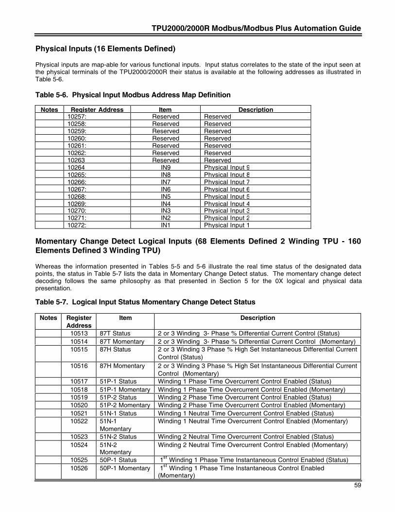
TPU2000/2000R Modbus/Modbus Plus Automation Guide
59
Physical Inputs (16 Elements Defined)
Physical inputs are map-able for various functional inputs. Input status correlates to the state of the input seen atthe physical terminals of the TPU2000/2000R their status is available at the following addresses as illustrated inTable 5-6.
Table 5-6. Physical Input Modbus Address Map Definition
Notes Register Address Item Description10257: Reserved Reserved10258: Reserved Reserved10259: Reserved Reserved10260: Reserved Reserved10261: Reserved Reserved10262: Reserved Reserved10263 Reserved Reserved10264 IN9 Physical Input 910265: IN8 Physical Input 810266: IN7 Physical Input 710267: IN6 Physical Input 610268: IN5 Physical Input 510269: IN4 Physical Input 410270: IN3 Physical Input 310271: IN2 Physical Input 210272: IN1 Physical Input 1
Momentary Change Detect Logical Inputs (68 Elements Defined 2 Winding TPU - 160Elements Defined 3 Winding TPU)
Whereas the information presented in Tables 5-5 and 5-6 illustrate the real time status of the designated datapoints, the status in Table 5-7 lists the data in Momentary Change Detect status. The momentary change detectdecoding follows the same philosophy as that presented in Section 5 for the 0X logical and physical datapresentation.
Table 5-7. Logical Input Status Momentary Change Detect Status
Notes RegisterAddress
Item Description
10513 87T Status 2 or 3 Winding 3- Phase % Differential Current Control (Status)10514 87T Momentary 2 or 3 Winding 3- Phase % Differential Current Control (Momentary)10515 87H Status 2 or 3 Winding 3 Phase % High Set Instantaneous Differential Current
Control (Status)10516 87H Momentary 2 or 3 Winding 3 Phase % High Set Instantaneous Differential Current
Control (Momentary)10517 51P-1 Status Winding 1 Phase Time Overcurrent Control Enabled (Status)10518 51P-1 Momentary Winding 1 Phase Time Overcurrent Control Enabled (Momentary)10519 51P-2 Status Winding 2 Phase Time Overcurrent Control Enabled (Status)10520 51P-2 Momentary Winding 2 Phase Time Overcurrent Control Enabled (Momentary)10521 51N-1 Status Winding 1 Neutral Time Overcurrent Control Enabled (Status)10522 51N-1
MomentaryWinding 1 Neutral Time Overcurrent Control Enabled (Momentary)
10523 51N-2 Status Winding 2 Neutral Time Overcurrent Control Enabled (Status)10524 51N-2
MomentaryWinding 2 Neutral Time Overcurrent Control Enabled (Momentary)
10525 50P-1 Status 1st Winding 1 Phase Time Instantaneous Control Enabled (Status)10526 50P-1 Momentary 1st Winding 1 Phase Time Instantaneous Control Enabled
(Momentary)
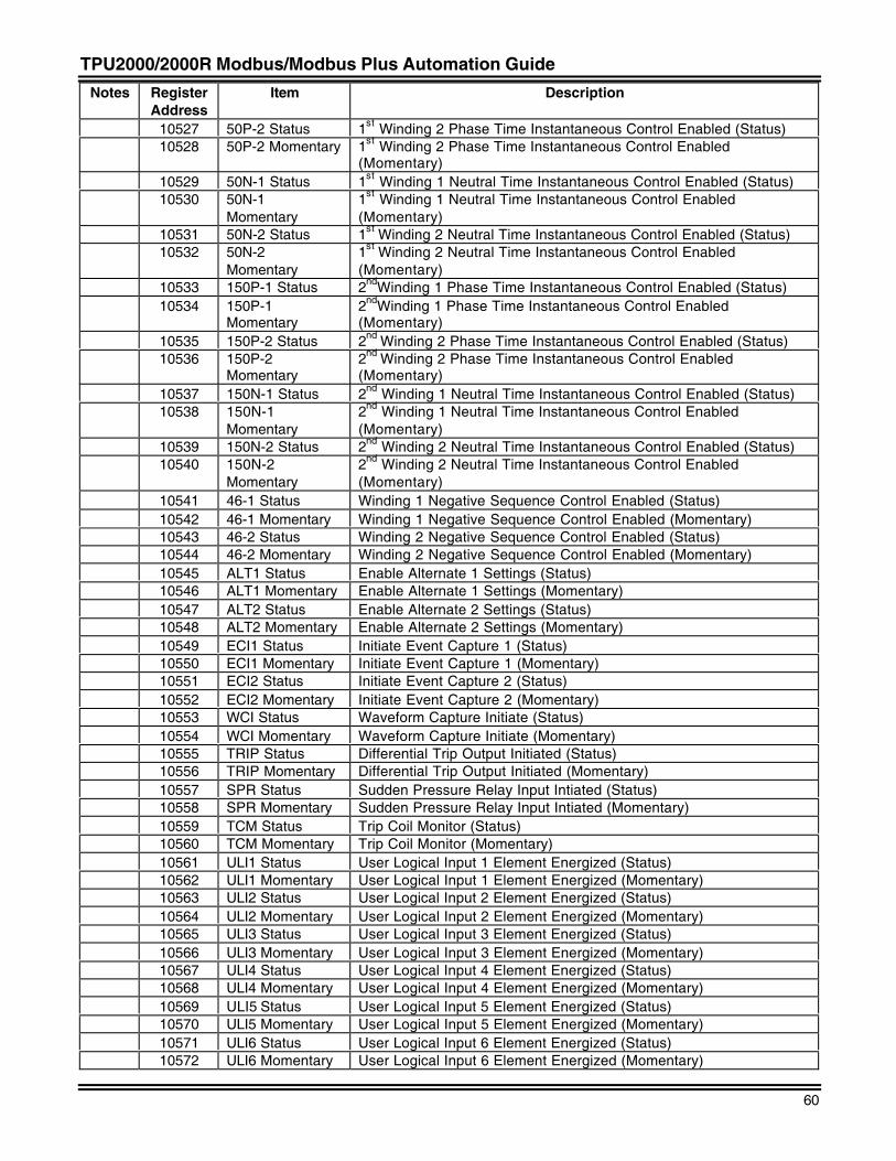
TPU2000/2000R Modbus/Modbus Plus Automation Guide
60
Notes RegisterAddress
Item Description
10527 50P-2 Status 1st Winding 2 Phase Time Instantaneous Control Enabled (Status)10528 50P-2 Momentary 1st Winding 2 Phase Time Instantaneous Control Enabled
(Momentary)10529 50N-1 Status 1st Winding 1 Neutral Time Instantaneous Control Enabled (Status)10530 50N-1
Momentary1st Winding 1 Neutral Time Instantaneous Control Enabled(Momentary)
10531 50N-2 Status 1st Winding 2 Neutral Time Instantaneous Control Enabled (Status)10532 50N-2
Momentary1st Winding 2 Neutral Time Instantaneous Control Enabled(Momentary)
10533 150P-1 Status 2ndWinding 1 Phase Time Instantaneous Control Enabled (Status)10534 150P-1
Momentary2ndWinding 1 Phase Time Instantaneous Control Enabled(Momentary)
10535 150P-2 Status 2nd Winding 2 Phase Time Instantaneous Control Enabled (Status)10536 150P-2
Momentary2nd Winding 2 Phase Time Instantaneous Control Enabled(Momentary)
10537 150N-1 Status 2nd Winding 1 Neutral Time Instantaneous Control Enabled (Status)10538 150N-1
Momentary2nd Winding 1 Neutral Time Instantaneous Control Enabled(Momentary)
10539 150N-2 Status 2nd Winding 2 Neutral Time Instantaneous Control Enabled (Status)10540 150N-2
Momentary2nd Winding 2 Neutral Time Instantaneous Control Enabled(Momentary)
10541 46-1 Status Winding 1 Negative Sequence Control Enabled (Status)10542 46-1 Momentary Winding 1 Negative Sequence Control Enabled (Momentary)10543 46-2 Status Winding 2 Negative Sequence Control Enabled (Status)10544 46-2 Momentary Winding 2 Negative Sequence Control Enabled (Momentary)10545 ALT1 Status Enable Alternate 1 Settings (Status)10546 ALT1 Momentary Enable Alternate 1 Settings (Momentary)10547 ALT2 Status Enable Alternate 2 Settings (Status)10548 ALT2 Momentary Enable Alternate 2 Settings (Momentary)10549 ECI1 Status Initiate Event Capture 1 (Status)10550 ECI1 Momentary Initiate Event Capture 1 (Momentary)10551 ECI2 Status Initiate Event Capture 2 (Status)10552 ECI2 Momentary Initiate Event Capture 2 (Momentary)10553 WCI Status Waveform Capture Initiate (Status)10554 WCI Momentary Waveform Capture Initiate (Momentary)10555 TRIP Status Differential Trip Output Initiated (Status)10556 TRIP Momentary Differential Trip Output Initiated (Momentary)10557 SPR Status Sudden Pressure Relay Input Intiated (Status)10558 SPR Momentary Sudden Pressure Relay Input Intiated (Momentary)10559 TCM Status Trip Coil Monitor (Status)10560 TCM Momentary Trip Coil Monitor (Momentary)10561 ULI1 Status User Logical Input 1 Element Energized (Status)10562 ULI1 Momentary User Logical Input 1 Element Energized (Momentary)10563 ULI2 Status User Logical Input 2 Element Energized (Status)10564 ULI2 Momentary User Logical Input 2 Element Energized (Momentary)10565 ULI3 Status User Logical Input 3 Element Energized (Status)10566 ULI3 Momentary User Logical Input 3 Element Energized (Momentary)10567 ULI4 Status User Logical Input 4 Element Energized (Status)10568 ULI4 Momentary User Logical Input 4 Element Energized (Momentary)10569 ULI5 Status User Logical Input 5 Element Energized (Status)10570 ULI5 Momentary User Logical Input 5 Element Energized (Momentary)10571 ULI6 Status User Logical Input 6 Element Energized (Status)10572 ULI6 Momentary User Logical Input 6 Element Energized (Momentary)
TPU2000/2000R Modbus/Modbus Plus Automation Guide
61
Notes RegisterAddress
Item Description
10573 ULI7 Status User Logical Input 7 Element Energized (Status)10574 ULI7 Momentary User Logical Input 7 Element Energized (Momentary)10575 ULI8 Status User Logical Input 8 Element Energized (Status)10576 ULI8 Momentary User Logical Input 8 Element Energized (Momentary)10577 ULI9 Status User Logical Input 9 Element Energized (Status)10578 ULI9 Momentary User Logical Input 9 Element Energized (Momentary)10579 CRI Status Reclose and Overcurrent Counters Cleared (Status)10580 CRI Momentary Reclose and Overcurrent Counters Cleared (Momentary)
3 10581 Reserved Reserved3 10582 Reserved Reserved3 10583 Reserved Reserved3 10584 Reserved Reserved3 10585 Reserved Reserved3 10586 Reserved Reserved3 10587 Reserved Reserved3 10588 Reserved Reserved3 10589 Reserved Reserved3 10590 Reserved Reserved3 10591 Reserved Reserved3 10592 Reserved Reserved3 10593 Reserved Reserved3 10594 Reserved Reserved3 10595 Reserved Reserved3 10596 Reserved Reserved3 10597 Reserved Reserved3 10598 Reserved Reserved3 10599 Reserved Reserved3 10600 Reserved Reserved3 10601: Reserved Reserved3 10602: Reserved Reserved3 10603: Reserved Reserved3 10604: Reserved Reserved3 10605: Reserved Reserved3 10606: Reserved Reserved3 10607: Reserved Reserved3 10608: Reserved Reserved3 10609: Reserved Reserved3 10610: Reserved Reserved3 10611: Reserved Reserved3 10612: Reserved Reserved3 10613: Reserved Reserved3 10614: Reserved Reserved3 10615: Reserved Reserved3 10616: Reserved Reserved3 10617: Reserved Reserved3 10618: Reserved Reserved3 10619: Reserved Reserved3 10620: Reserved Reserved3 10621: Reserved Reserved3 10622: Reserved Reserved3 10623: Reserved Reserved3 10624: Reserved Reserved3 10625: Reserved Reserved
TPU2000/2000R Modbus/Modbus Plus Automation Guide
62
Notes RegisterAddress
Item Description
3 10626: Reserved Reserved3 10627: Reserved Reserved3 10628: Reserved Reserved3 10629: Reserved Reserved3 10630: Reserved Reserved3 10631: Reserved Reserved3 10632: Reserved Reserved3 10633: Reserved Reserved3 10634: Reserved Reserved3 10635: Reserved Reserved3 10636: Reserved Reserved3 10637: Reserved Reserved3 10638: Reserved Reserved3 10639 Reserved Reserved3 10640: Reserved Reserved3 10641: 51P-3 Status Winding 3 Phase Time Overcurrent Control Enabled (Status)3 10642: 51P-3 Momentary Winding 3 Phase Time Overcurrent Control Enabled (Momentary)3 10643: 51N-3 Status Winding 3 Neutral Time Overcurrent Control Enabled (Status)3 10644: 51N-3
MomentaryWinding 3 Neutral Time Overcurrent Control Enabled (Momentary)
3 10645: 50P-3 Status 1st Winding 3 Phase Time Instantaneous Control Enabled (Status)3 10646: 50P-3 Momentary 1st Winding 3 Phase Time Instantaneous Control Enabled
(Momentary)3 10647: 50N-3 Status 1st Winding 3 Neutral Time Instantaneous Control Enabled (Status)3 10648: 50N-3
Momentary1st Winding 3 Neutral Time Instantaneous Control Enabled(Momentary)
3 10649: 150P-3 Status 2nd Winding 3 Phase Time Instantaneous Control Enabled (Status)3 10650: 150P-3
Momentary2nd Winding 3 Phase Time Instantaneous Control Enabled(Momentary)
3 10651: 150N-3 Status 2nd Winding 3 Neutral Time Instantaneous Control Enabled (Status)3 10652: 150N-3
Momentary2nd Winding 3 Neutral Time Instantaneous Control Enabled(Momentary)
3 10653: 46-3 Status Winding 3 Negative Sequence Control Enabled (Status)3 10654: 46-3 Momentary Winding 3 Negative Sequence Control Enabled (Momentary)3 10655: 51G Status Ground Time Overcurrent Control Enabled (Status)3 10656: 51G Momentary Ground Time Overcurrent Control Enabled (Momentary)3 10657: 50G Status Ground Time Instantaneous Control Enabled (Status)3 10658: 50G Momentary Ground Time Instantaneous Control Enabled (Momentary)3 10659: 150G Status 2nd Ground Time Instantaneous Control Enabled (Status)3 10660: 150G Momentary 2nd Ground Time Instantaneous Control Enabled (Momentary)3 10661: ECI3 Status Event Capture Initiate Enabled (Status)3 10662: ECI3 Momentary Event Capture Initiate Enabled (Momentary)3 10663: Reserved Reserved3 10664: Reserved Reserved3 10665: Reserved Reserved3 10666: Reserved Reserved3 10667: Reserved Reserved3 10668: Reserved Reserved3 10669: Reserved Reserved3 10670: Reserved Reserved3 10671: Reserved Reserved3 10672: Reserved Reserved
3= Three Winding TPU Only
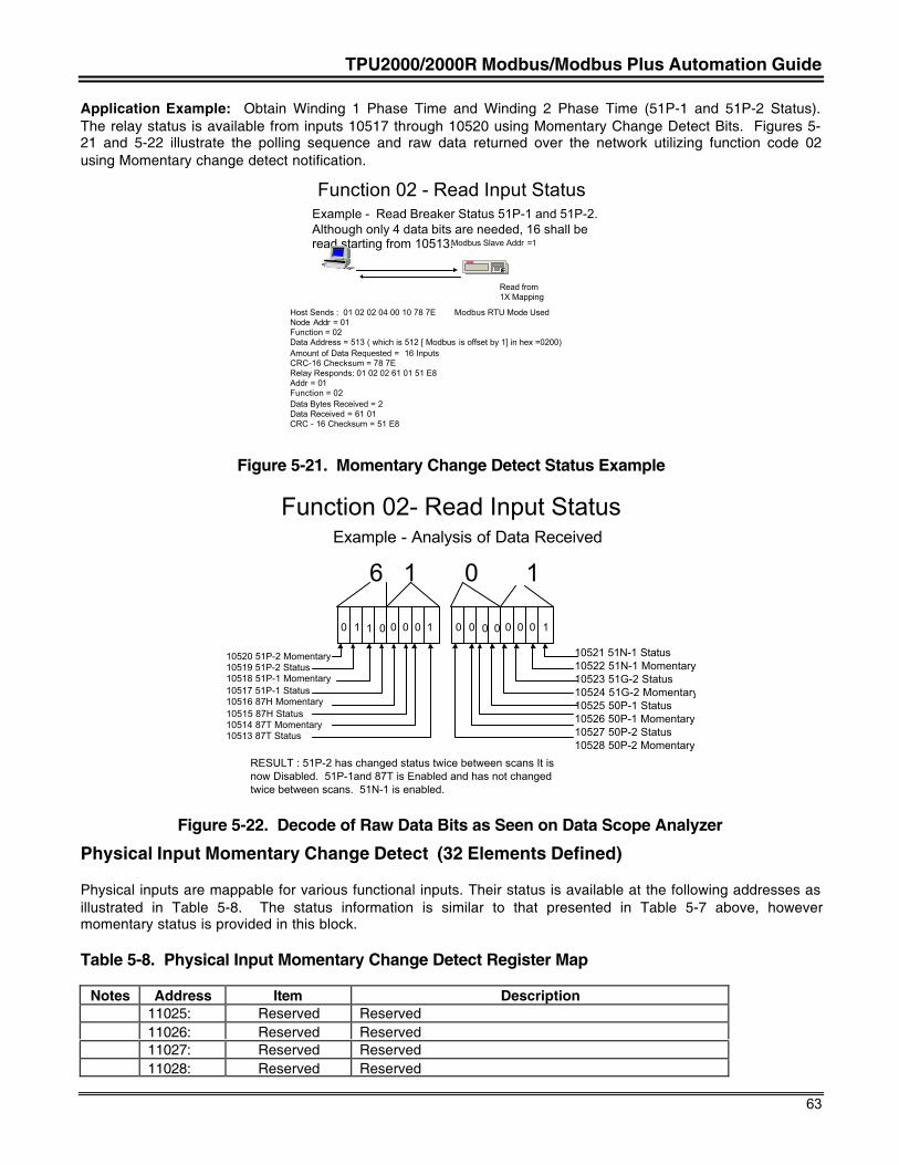
TPU2000/2000R Modbus/Modbus Plus Automation Guide
63
Application Example: Obtain Winding 1 Phase Time and Winding 2 Phase Time (51P-1 and 51P-2 Status).The relay status is available from inputs 10517 through 10520 using Momentary Change Detect Bits. Figures 5-21 and 5-22 illustrate the polling sequence and raw data returned over the network utilizing function code 02using Momentary change detect notification.
Function 02 - Read Input StatusExample - Read Breaker Status 51P-1 and 51P-2.Although only 4 data bits are needed, 16 shall beread starting from 10513.Modbus Slave Addr =1
Host Sends : 01 02 02 04 00 10 78 7E Modbus RTU Mode UsedNode Addr = 01Function = 02 Data Address = 513 ( which is 512 [ Modbus is offset by 1] in hex =0200)Amount of Data Requested = 16 InputsCRC-16 Checksum = 78 7ERelay Responds: 01 02 02 61 01 51 E8Addr = 01Function = 02Data Bytes Received = 2Data Received = 61 01CRC - 16 Checksum = 51 E8
Read from 1X Mapping
EC
Figure 5-21. Momentary Change Detect Status Example
Function 02- Read Input Status
0 1 1 0 0 0 0 1 0 0 0 0 0 0 0 1
Example - Analysis of Data Received
6 1 0 1
10520 51P-2 Momentary10519 51P-2 Status10518 51P-1 Momentary10517 51P-1 Status10516 87H Momentary10515 87H Status10514 87T Momentary10513 87T Status
10521 51N-1 Status10522 51N-1 Momentary10523 51G-2 Status10524 51G-2 Momentary10525 50P-1 Status10526 50P-1 Momentary10527 50P-2 Status10528 50P-2 Momentary
RESULT : 51P-2 has changed status twice between scans It is now Disabled. 51P-1and 87T is Enabled and has not changed twice between scans. 51N-1 is enabled.
Figure 5-22. Decode of Raw Data Bits as Seen on Data Scope Analyzer
Physical Input Momentary Change Detect (32 Elements Defined)
Physical inputs are mappable for various functional inputs. Their status is available at the following addresses asillustrated in Table 5-8. The status information is similar to that presented in Table 5-7 above, howevermomentary status is provided in this block.
Table 5-8. Physical Input Momentary Change Detect Register Map
Notes Address Item Description11025: Reserved Reserved11026: Reserved Reserved11027: Reserved Reserved11028: Reserved Reserved
TPU2000/2000R Modbus/Modbus Plus Automation Guide
64
Notes Address Item Description11029: Reserved Reserved11030: Reserved Reserved11031: Reserved Reserved11032: Reserved Reserved11033: Reserved Reserved11034: Reserved Reserved11035: Reserved Reserved11036: Reserved Reserved11037: Reserved Reserved11038: Reserved Reserved11039: Reserved Reserved11040: Reserved Reserved11041: IN8 Status Physical Input 8 Status11042: IN8 Momentary Physical Input 8 (Momentary)11043: IN7 Status Physical Input 7 Status11044: IN7 Momentary Physical Input 7 (Momentary)11045: IN6 Status Physical Input 6 Status11046: IN6 Momentary Physical Input 6 Change Detect Between Host Scan11047: IN5 Status Physical Input 5 Status11048: IN5 Momentary Physical Input 5 Change Detect Between Host Scan11049: IN4 Status Physical Input 4 Status11050: IN4 Momentary Physical Input 4 Change Detect Between Host Scan11051: IN3 Status Physical Input 3 Status11052: IN3 Momentary Physical Input 3 Change Detect Between Host Scan11053: IN2 Status Physical Input 2 Status11054: IN2 Momentary Physical Input 2 Change Detect Between Host Scan11055: IN1 Status Physical Input 1 Status11056: IN1 Momentary Physical Input 1 Change Detect Between Host Scan
4X Register Read Capabilities
The TPU2000/2000R implementation of 4X registers allow for both status reads and in limited cases for controlregister writes. Many host devices do not allow the access of data from discrete data types (such as 0X and 1Xdiscrete output and input function codes). The Modbus implementation within the TPU2000/2000R relay allowsfor Modbus commands 03, 16 (10 hex) and 23 (17 hex) register commands. Real time relay status is available forthe following relay data types and functionality:
• Relay Status• Diagnostic Status• Unit Information• CT and PT Information• Physical Input Status• Logical Input Status• Physical Output Status• Logical Output Status• Load Metering Data• Demand Metering Data• Master Trip Functionality• Fault Record Buffering (1- 32)• Event Record Buffering (1- 128)• Breaker Counter Operation Retrieval• Force of Physical Outputs• Breaker Control Functions over the network• Reset of Counter, Event Buffer, Operational Buffer, Seal In and Target information.
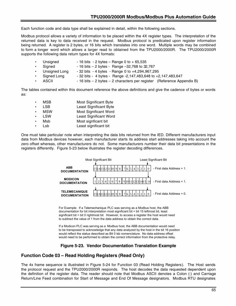
TPU2000/2000R Modbus/Modbus Plus Automation Guide
65
Each function code and data type shall be explained in detail, within the following sections.
Modbus protocol allows a variety of information to be placed within the 4X register types. The interpretation of thereturned data is key to data received in the request. Modbus protocol is predicated upon register informationbeing returned. A register is 2 bytes, or 16 bits which translates into one word. Multiple words may be combinedto form a longer word which allows a larger read to obtained from the TPU2000/2000R. The TPU2000/2000Rsupports the following data return types for 4X formats:
• Unsigned - 16 bits - 2 bytes – Range 0 to + 65,535• Signed - 16 bits – 2 bytes - Range –32,768 to 32,767• Unsigned Long - 32 bits - 4 bytes - Range 0 to +4,294,967,295• Signed Long - 32 bits - 4 bytes - Range -2,147,483,648 to +2,147,483,647• ASCII - 16 bits – 2 bytes – 2 characters per register (Reference Appendix B)
The tables contained within this document reference the above definitions and give the cadence of bytes or wordsas:
• MSB Most Significant Byte• LSB Least Significant Byte• MSW Most Significant Word• LSW Least Significant Word• Msb Most signficant bit• Lsb Least significant bit
One must take particular note when interpreting the data bits returned from the IED. Different manufacturers inputdata from Modbus devices however, each manufacturer starts its address start addresses taking into account thezero offset whereas, other manufacturers do not. Some manufacturers number their data bit presentations in theregisters differently. Figure 5-23 below illustrates the register decoding differences.
ABB DOCUMENTATION
Most Significant Bit Least Significant Bit
151413 12 11 10 9 8 7 6 5 4 3 2 1 0 - First data Address = 1.
MODICON DOCUMENTATION 1 2 3 4 5 6 7 8 9 10 11 12 13 1415 16 - First data Address = 1.
TELEMECANIQUEDOCUMENTATION 151413 12 11 10 9 8 7 6 5 4 3 2 1 0 - First data Address = 0.
For Example: If a Telemechanique PLC was serving as a Modbus host, the ABBdocumentation for bit interpretation most significant bit = bit 15 leftmost bit, leastsignificant bit = bit 0 rightmost bit. However, to access a register the host would needto subtract the value of 1 from the data address to obtain the correct data.
If a Modicon PLC was serving as a Modbus host, the ABB documentation would needto be transposed to acknowledge that any data analyzed by the host in the bit 16 positionwould reflect the status described as Bit 0 lsb nomenclature. No data address offsetwould need to be performed to obtain the correct information from the protective relay.
Figure 5-23. Vendor Documentation Translation Example
Function Code 03 – Read Holding Registers (Read Only)
The 4x frame sequence is illustrated in Figure 5-24 for Function 03 (Read Holding Registers). The Host sendsthe protocol request and the TPU2000/2000R responds. The host decodes the data requested dependent uponthe definition of the register data. The reader should note that Modbus ASCII denotes a Colon (:) and CarriageReturn/Line Feed combination for Start of Message and End Of Message designators. Modbus RTU designates
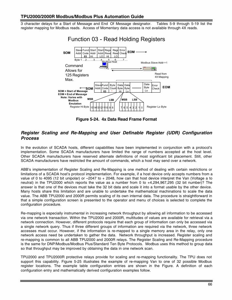
TPU2000/2000R Modbus/Modbus Plus Automation Guide
66
3 character delays for a Start of Message and End Of Message designator. Tables 5-9 through 5-19 list theregister mapping for Modbus reads. Access of Momentary data access is not available through 4X reads.
Function 03 - Read Holding Registers
Modbus Host Modbus Slave Addr =1
Read from 4X Mapping
SlaveAddr.
Funct.Code 03
StartAddrHI
Start Addr LO
RegsRead HI
RegsRead LO
ErrorCheck EOMSOM
Byte 1 …2……..3…….4…….5……6……..7….
Register Lo Byte
CommandAllows for125 RegistersMax.
SlaveAddr.
Funct.Code 03
ByteCount *
DataByte Hi
DataByte Lo
DataByte Lo
ErrorCheck EOMSOM
MSB LSB
151413121110 9 8 7 6 5 4 3 2 1 0
MSB LSB
Register Hi Byte
SOM = Start of MessageEOM = End of Message Note: Varies with Modbus Emulation
EC
Figure 5-24. 4x Data Read Frame Format
Register Scaling and Re-Mapping and User Definable Register (UDR) ConfigurationProcess
In the evolution of SCADA hosts, different capabilities have been implemented in conjunction with a protocol’simplementation. Some SCADA manufacturers have limited the range of numbers accepted at the host level.Other SCADA manufacturers have reserved alternate definitions of most significant bit placement. Still, otherSCADA manufacturers have restricted the amount of commands, which a host may send over a network.
ABB’s implementation of Register Scaling and Re-Mapping is one method of dealing with certain restrictions orlimitations of a SCADA host’s protocol implementation. For example, if a host device only accepts numbers from avalue of 0 to 4095 (12 bit unipolar) or –2047 to + 2048, how can that host device interpret the Van (Voltage a toneutral) in the TPU2000 which reports the value as a number from 0 to +4,294,967,295 (32 bit number)? Theanswer is that one of the devices must take the 32 bit data and scale it into a format usable by the other device.Many hosts share this limitation and are unable to undertake the mathematical machinations to scale the datavalue. The ABB TPU2000 and 2000R permits scaling of its own internal data. The procedure is straightforward inthat a simple configuration screen is presented to the operator and menu of choices is selected to complete theconfiguration procedure.
Re-mapping is especially instrumental in increasing network throughput by allowing all information to be accessedvia one network transaction. Within the TPU2000 and 2000R, multitudes of values are available for retrieval via anetwork connection. However, different protocols require that each group of information can only be accessed viaa single network query. Thus if three different groups of information are required via the network, three networkaccesses must occur. However, if the information is re-mapped to a single memory area in the relay, only onenetwork access need be undertaken to gather the data. Network throughput is increased. Register scaling andre-mapping is common to all ABB TPU2000 and 2000R relays. The Register Scaling and Re-Mapping procedureis the same for DNP/Modbus/Modbus Plus/Standard Ten Byte Protocols. Modbus uses this method to group dataso that throughput may be improved by obtaining the data in one network scan.
TPU2000 and TPU2000R protective relays provide for scaling and re-mapping functionality. The TPU does notsupport this capability. Figure 5-25 illustrates the example of re-mapping Van to one of 32 possible Modbusregister locations. The example table configuration entries are shown in the Figure. A definition of eachconfiguration entry and mathematically derived configuration examples follow.

TPU2000/2000R Modbus/Modbus Plus Automation Guide
67
TPU2000 and 2000R Internal Operation
The TPU2000 and TPU2000R reads the raw analog values received from the CT and PT physical connections.The microprocessor-based relay then converts the analog values to a raw digital numeric value from the relay’sinternal Analog to Digital Converter (A/D) hardware platform. The conversion of the voltage and current readingsis not complete. The TPU2000 and TPU2000R microprocessor then takes the raw converted value and performsa mathematical calculation providing a numeric value which is displayed on the relay’s front panel MMI or throughnetwork accesses.
A protection engineer would recognize the terms as such:
PRIMARY VALUES – the metering values displayed on the protective relay’s front panel interface.
SECONDARY VALUES – the current or voltage received by the CT or PT attached to the unit.
SCALED VALUES – the value received by the host device (or calculated by the IED and transmitted to the host)through the communication interface.
The mathematical calculations involved require the CT Phase, CT Neutral, and PT ratios in order to convert theraw A/D to an understandable value, displayed on the front panel MMI or available for access via a networkconnection. Thus, the information Van (Voltage A to Neutral), is displayed on the front panel MMI is in convertedformat (not raw A/D readings), and the data received via the Modbus/Modbus Plus Registers (40265 and 40266)is reported in Volts in a 32 bit representation. The maximum value able to be physically metered by the relay isdependent upon the TPU2000/2000R and the ratio of the PT and CT’s used. The CT and PT values are enteredinto the TPU through ECP/WinECP in the Configuration Settings Menu illustrated in Figure 5-14. However, life aswe know it, is not perfect. Many SCADA hosts are unable to interpret the 32-bit value received over a network.What can be done? ABB’s answer is to provide for a fill-in-the-blanks method of scaling. This method takes theinterpreted value and provides for DIVISOR SCALING (taking the MMI/network register values and dividing by aconstant) or a RATIO SCALING (taking the MMI values/network register values, PT Ratios, CT Ratios and FullSCALE Metered Readings) and transform it into a raw scaled value depending on the minimum/maximum valuethe SCADA system can interpret. The SCADA system must then receive the mathematical value and perform itsown internal calculations so that the data may be displayed to the operator which mirrors that displayed on therelay’s front panel.
E
CNORMALFAILP ICKUPR E C L O S E R O U T
S Y S T E M R E S E T
TIMEINSTANTANEOUSFREQUENCYNEGATIVE SEQUENCE
TARGET RESET
STATUS T A R G E T S
ABCN
DPU2000R
N e t w o r k
PartnerV1.0
TPU2000R
32Mappable Registers
Change Register Configuration
400001
400002
400003
400004
400005
400032
User Definable Register 40005
Scale 500Source Register Address (4XXX) 265Destination Data Type Bipolar (LSB)Destination Data Size 12 BitSource Scale Type VoltageSource Data Type Unsigned 32 Bit
To Accept Changes: Press Enter Return
No Change: Press Escape Key
High Word Van
Low Word Van
40265
40266
TYPICAL SCALING EXAMPLE
Figure 5-25. Register Scaling Methodology
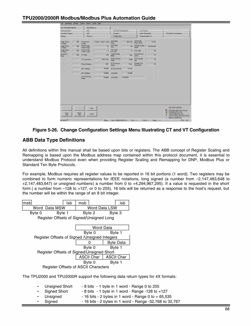
TPU2000/2000R Modbus/Modbus Plus Automation Guide
68
Figure 5-26. Change Configuration Settings Menu Illustrating CT and VT Configuration
ABB Data Type Definitions
All definitions within this manual shall be based upon bits or registers. The ABB concept of Register Scaling andRemapping is based upon the Modbus address map contained within this protocol document, it is essential tounderstand Modbus Protocol even when providing Register Scaling and Remapping for DNP, Modbus Plus orStandard Ten Byte Protocols.
For example, Modbus requires all register values to be reported in 16 bit portions (1 word). Two registers may becombined to form numeric representations for IEEE notations, long signed (a number from –2,147,483,648 to+2,147,483,647) or unsigned numbers( a number from 0 to +4,294,967,295). If a value is requested in the shortform ( a number from –128 to +127, or 0 to 255), 16 bits will be returned as a response to the host’s request, butthe number will be within the range of an 8 bit integer.
msb lsb msb lsbWord Data MSW Word Data LSW
Byte 0 Byte 1 Byte 2 Byte 3Register Offsets of Signed/Unsigned Long
Word Data Byte 0 Byte 1
Register Offsets of Signed /Unsigned Integers0 Byte Data
Byte 0 Byte 1Register Offsets of Signed/Unsigned Short
ASCII Char ASCII CharByte 0 Byte 1
Register Offsets of ASCII Characters
The TPU2000 and TPU2000R support the following data return types for 4X formats:
• Unsigned Short - 8 bits - 1 byte in 1 word - Range 0 to 255• Signed Short - 8 bits - 1 byte in 1 word - Range -128 to +127• Unsigned - 16 bits - 2 bytes in 1 word - Range 0 to + 65,535• Signed - 16 bits - 2 bytes in 1 word - Range -32,768 to 32,767
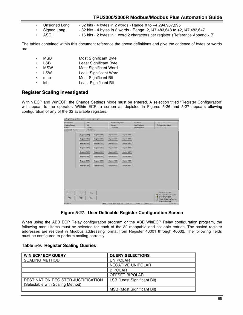
TPU2000/2000R Modbus/Modbus Plus Automation Guide
69
• Unsigned Long - 32 bits - 4 bytes in 2 words - Range 0 to +4,294,967,295• Signed Long - 32 bits - 4 bytes in 2 words - Range -2,147,483,648 to +2,147,483,647• ASCII - 16 bits - 2 bytes in 1 word 2 characters per register (Reference Appendix B)
The tables contained within this document reference the above definitions and give the cadence of bytes or wordsas:
• MSB Most Significant Byte• LSB Least Significant Byte• MSW Most Significant Word• LSW Least Significant Word• msb Most Significant Bit• lsb Least Significant Bit
Register Scaling Investigated
Within ECP and WinECP, the Change Settings Mode must be entered. A selection titled “Register Configuration”will appear to the operator. Within ECP, a screen as depicted in Figures 5-26 and 5-27 appears allowingconfiguration of any of the 32 available registers.
Figure 5-27. User Definable Register Configuration Screen
When using the ABB ECP Relay configuration program or the ABB WinECP Relay configuration program, thefollowing menu items must be selected for each of the 32 mappable and scalable entries. The scaled registeraddresses are resident in Modbus addressing format from Register 40001 through 40032. The following fieldsmust be configured to perform scaling correctly:
Table 5-9. Register Scaling Queries
WIN ECP/ ECP QUERY QUERY SELECTIONSSCALING METHOD UNIPOLAR
NEGATIVE UNIPOLARBIPOLAROFFSET BIPOLAR
DESTINATION REGISTER JUSTIFICATION(Selectable with Scaling Method)
LSB (Least Significant Bit)
MSB (Most Significant Bit)
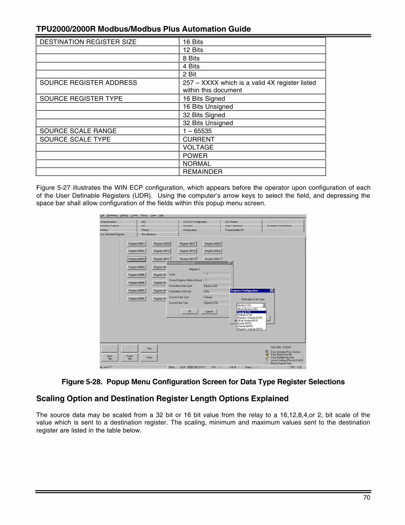
TPU2000/2000R Modbus/Modbus Plus Automation Guide
70
DESTINATION REGISTER SIZE 16 Bits12 Bits8 Bits4 Bits2 Bit
SOURCE REGISTER ADDRESS 257 – XXXX which is a valid 4X register listedwithin this document
SOURCE REGISTER TYPE 16 Bits Signed16 Bits Unsigned32 Bits Signed32 Bits Unsigned
SOURCE SCALE RANGE 1 – 65535SOURCE SCALE TYPE CURRENT
VOLTAGEPOWERNORMALREMAINDER
Figure 5-27 illustrates the WIN ECP configuration, which appears before the operator upon configuration of eachof the User Definable Registers (UDR). Using the computer’s arrow keys to select the field, and depressing thespace bar shall allow configuration of the fields within this popup menu screen.
Figure 5-28. Popup Menu Configuration Screen for Data Type Register Selections
Scaling Option and Destination Register Length Options Explained
The source data may be scaled from a 32 bit or 16 bit value from the relay to a 16,12,8,4,or 2, bit scale of thevalue which is sent to a destination register. The scaling, minimum and maximum values sent to the destinationregister are listed in the table below.
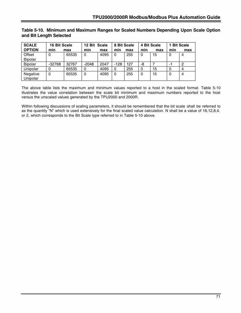
TPU2000/2000R Modbus/Modbus Plus Automation Guide
71
Table 5-10. Minimum and Maximum Ranges for Scaled Numbers Depending Upon Scale Optionand Bit Length Selected
SCALEOPTION
16 Bit Scalemin max
12 Bit Scalemin max
8 Bit Scalemin max
4 Bit Scalemin max
1 Bit Scalemin max
OffsetBipolar
0 65535 0 4095 0 255 0 15 0 4
Bipolar -32768 32767 -2048 2047 -128 127 -8 7 -1 2Unipolar 0 65535 0 4095 0 255 0 15 0 4NegativeUnipolar
0 65535 0 4095 0 255 0 15 0 4
The above table lists the maximum and minimum values reported to a host in the scaled format. Table 5-10illustrates the value correlation between the scale bit minimum and maximum numbers reported to the hostversus the unscaled values generated by the TPU2000 and 2000R.
Within following discussions of scaling parameters, it should be remembered that the bit scale shall be referred toas the quantity “N” which is used extensively for the final scaled value calculation. N shall be a value of 16,12,8,4,or 2, which corresponds to the Bit Scale type referred to in Table 5-10 above.
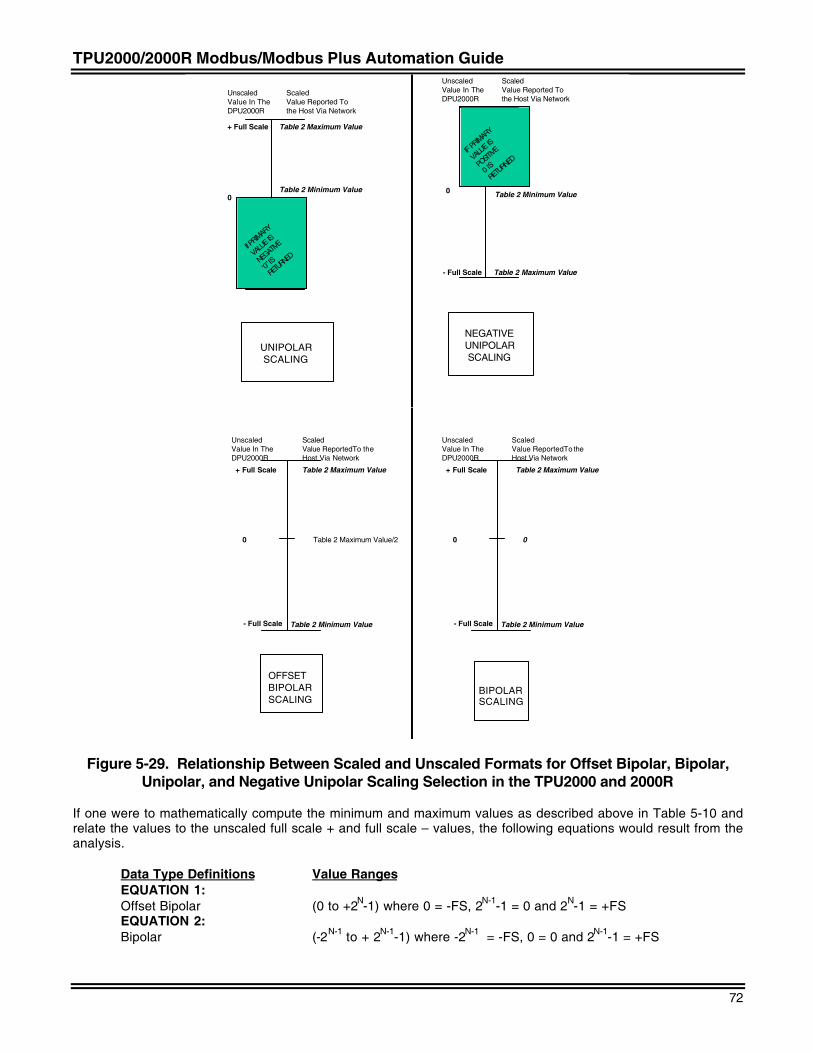
TPU2000/2000R Modbus/Modbus Plus Automation Guide
72
UnscaledValue In TheDPU2000R
Scaled Value Reported To the Host Via Network
0
+ Full Scale
Table 2 Minimum Value
Table 2 Maximum Value
If PRIMAR
Y
VALU
E IS
NEGAT
IVE
‘0” IS
RETU
RNED
UNIPOLAR SCALING
UnscaledValue In TheDPU2000R
Scaled Value Reported To the Host Via Network
0
- Full Scale
Table 2 Minimum Value
Table 2 Maximum Value
IF PRIMAR
Y
VALU
E IS
POSIT
IVE
0 IS
RETURNED
NEGATIVEUNIPOLAR SCALING
UnscaledValue In TheDPU2000R
Scaled Value ReportedTo the Host Via Network
- Full Scale
0
+ Full Scale
Table 2 Minimum Value
0
BIPOLARSCALING
UnscaledValue In TheDPU2000R
Scaled Value ReportedTo the Host Via Network
- Full Scale
0
+ Full Scale
Table 2 Minimum Value
Table 2 Maximum Value/2
OFFSETBIPOLARSCALING
Table 2 Maximum Value Table 2 Maximum Value
Figure 5-29. Relationship Between Scaled and Unscaled Formats for Offset Bipolar, Bipolar,Unipolar, and Negative Unipolar Scaling Selection in the TPU2000 and 2000R
If one were to mathematically compute the minimum and maximum values as described above in Table 5-10 andrelate the values to the unscaled full scale + and full scale – values, the following equations would result from theanalysis.
Data Type Definitions Value RangesEQUATION 1:Offset Bipolar (0 to +2N-1) where 0 = -FS, 2N-1-1 = 0 and 2N-1 = +FSEQUATION 2:Bipolar (-2N-1 to + 2N-1-1) where -2N-1 = -FS, 0 = 0 and 2N-1-1 = +FS
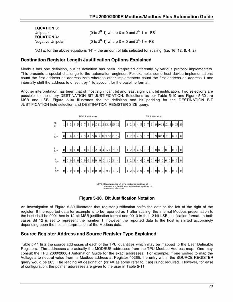
TPU2000/2000R Modbus/Modbus Plus Automation Guide
73
EQUATION 3:Unipolar (0 to 2N-1) where 0 = 0 and 2N-1 = +FSEQUATION 4:Negative Unipolar (0 to 2N-1) where 0 = 0 and 2N-1 = -FS
NOTE: for the above equations “N” = the amount of bits selected for scaling (i.e. 16, 12, 8, 4, 2)
Destination Register Length Justification Options Explained
Modbus has one definition, but its definition has been interpreted differently by various protocol implementers.This presents a special challenge to the automation engineer. For example, some host device implementationscount the first address as address zero whereas other implementers count the first address as address 1 andinternally shift the address to offset it by 1 to account for the baseline format.
Another interpretation has been that of most significant bit and least significant bit justification. Two selections arepossible for the query DESTINATION BIT JUSTIFICATION. Selections as per Table 5-10 and Figure 5-30 areMSB and LSB. Figure 5-30 illustrates the bit definition and bit padding for the DESTINATION BITJUSTIFICATION field selection and DESTINATION REGISTER SIZE query.
1 2 3 4 5 6 7 8 9 10 11 12 1314 15 16 1 2 3 4 5 6 7 8 9 101112 13 14 15 1616BIT
MSB Justification LSB Justification
NOTE : Bit designated as a 1 is the words most significant bit whereas the highest bit number is the least significant bit. 0 indicates a padded bit.
0 0 0 0 1 2 3 4 5 6 7 8 9 10 11 12 1 2 3 4 5 6 7 8 9 101112 0 0 0 012BIT
0 0 0 0 0 0 0 0 1 2 3 4 5 6 7 8 1 2 3 4 5 6 7 8 0 0 0 0 0 0 0 08BIT
0 0 0 0 0 0 0 0 0 0 0 0 1 2 3 4 1 2 3 4 0 0 0 0 0 0 0 0 0 0 0 04BIT
0 0 0 0 0 0 0 0 0 0 0 0 0 0 1 2 1 2 0 0 0 0 0 0 0 0 0 0 0 0 0 02BIT
Figure 5-30. Bit Justification Notation
An investigation of Figure 5-30 illustrates that register justification shifts the data to the left of the right of theregister. If the reported data for example is to be reported as 1 after scaling, the internal Modbus presentation tothe host shall be 0001 hex in 12 bit MSB justification format and 0010 in the 12 bit LSB justification format. In bothcases Bit 12 is set to represent the number 1, however the reported data to the host is shifted accordinglydepending upon the hosts interpretation of the Modbus data.
Source Register Address and Source Register Type Explained
Table 5-11 lists the source addresses of each of the TPU quantities which may be mapped to the User DefinableRegisters. The addresses are actually the MODBUS addresses from the TPU Modbus Address map. One mayconsult the TPU 2000/2000R Automation Guide for the exact addresses. For example, if one wished to map theVoltage a to neutral value from its Modbus address at Register 40265, the entry within the SOURCE REGISTERquery would be 265. The leading 40 designation (or 4X as some refer to it as) is not required. However, for easeof configuration, the pointer addresses are given to the user in Table 5-11.
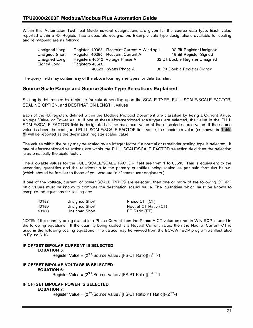
TPU2000/2000R Modbus/Modbus Plus Automation Guide
74
Within this Automation Technical Guide several designations are given for the source data type. Each valuereported within a 4X Register has a separate designation. Example data type designations available for scalingand re-mapping are as follows:
Unsigned Long Register 40385 Restraint Current A Winding 1 32 Bit Register UnsignedUnsigned Short Register 40260 Restraint Current A 16 Bit Register SignedUnsigned Long Registers 40513 Voltage Phase A 32 Bit Double Register UnsignedSigned Long Registers 40528
40528 kWatts Phase A 32 Bit Double Register Signed
The query field may contain any of the above four register types for data transfer.
Source Scale Range and Source Scale Type Selections Explained
Scaling is determined by a simple formula depending upon the SCALE TYPE, FULL SCALE/SCALE FACTOR,SCALING OPTION, and DESTINATION LENGTH, values.
Each of the 4X registers defined within the Modbus Protocol Document are classified by being a Current Value,Voltage Value, or Power Value. If one of these aforementioned scale types are selected, the value in the FULLSCALE/SCALE FACTOR field is designated as the maximum value of the unscaled source value. If the sourcevalue is above the configured FULL SCALE/SCALE FACTOR field value, the maximum value (as shown in TableX) will be reported as the destination register scaled value.
The values within the relay may be scaled by an integer factor if a normal or remainder scaling type is selected. Ifone of aforementioned selections are within the FULL SCALE/SCALE FACTOR selection field then the selectionis automatically the scale factor.
The allowable values for the FULL SCALE/SCALE FACTOR field are from 1 to 65535. This is equivalent to thesecondary quantities and the relationship to the primary quantities being scaled as per said formulas below.(which should be familiar to those of you who are “old” transducer engineers.)
If one of the voltage, current, or power SCALE TYPES are selected, then one or more of the following CT /PTratio values must be known to compute the destination scaled value. The quantities which must be known tocompute the equations for scaling are:
40158: Unsigned Short Phase CT (CT)40159: Unsigned Short Neutral CT Ratio (CT)40160: Unsigned Short PT Ratio (PT)
NOTE: If the quantity being scaled is a Phase Current then the Phase A CT value entered in WIN ECP is used inthe following equations. If the quantity being scaled is a Neutral Current value, then the Neutral Current CT isused in the following scaling equations. The values may be viewed from the ECP/WinECP program as illustratedin Figure 5-16.
IF OFFSET BIPOLAR CURRENT IS SELECTEDEQUATION 5:
Register Value = (2N-1*Source Value / [FS*CT Ratio])+2N-1-1
IF OFFSET BIPOLAR VOLTAGE IS SELECTEDEQUATION 6:
Register Value = (2N-1*Source Value / [FS*PT Ratio])+2N-1-1
IF OFFSET BIPOLAR POWER IS SELECTEDEQUATION 7:
Register Value = (2N-1*Source Value / [FS*CT Ratio*PT Ratio])+2N-1-1
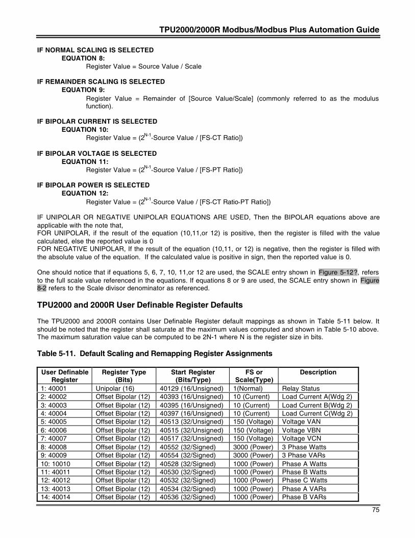
TPU2000/2000R Modbus/Modbus Plus Automation Guide
75
IF NORMAL SCALING IS SELECTEDEQUATION 8:
Register Value = Source Value / Scale
IF REMAINDER SCALING IS SELECTEDEQUATION 9:
Register Value = Remainder of [Source Value/Scale] (commonly referred to as the modulusfunction).
IF BIPOLAR CURRENT IS SELECTEDEQUATION 10:
Register Value = (2N-1*Source Value / [FS*CT Ratio])
IF BIPOLAR VOLTAGE IS SELECTEDEQUATION 11:
Register Value = (2N-1*Source Value / [FS*PT Ratio])
IF BIPOLAR POWER IS SELECTEDEQUATION 12:
Register Value = (2N-1*Source Value / [FS*CT Ratio*PT Ratio])
IF UNIPOLAR OR NEGATIVE UNIPOLAR EQUATIONS ARE USED, Then the BIPOLAR equations above areapplicable with the note that,FOR UNIPOLAR, if the result of the equation (10,11,or 12) is positive, then the register is filled with the valuecalculated, else the reported value is 0FOR NEGATIVE UNIPOLAR, If the result of the equation (10,11, or 12) is negative, then the register is filled withthe absolute value of the equation. If the calculated value is positive in sign, then the reported value is 0.
One should notice that if equations 5, 6, 7, 10, 11,or 12 are used, the SCALE entry shown in Figure 5-12?, refersto the full scale value referenced in the equations. If equations 8 or 9 are used, the SCALE entry shown in Figure8-2 refers to the Scale divisor denominator as referenced.
TPU2000 and 2000R User Definable Register Defaults
The TPU2000 and 2000R contains User Definable Register default mappings as shown in Table 5-11 below. Itshould be noted that the register shall saturate at the maximum values computed and shown in Table 5-10 above.The maximum saturation value can be computed to be 2N-1 where N is the register size in bits.
Table 5-11. Default Scaling and Remapping Register Assignments
User DefinableRegister
Register Type(Bits)
Start Register(Bits/Type)
FS orScale(Type)
Description
1: 40001 Unipolar (16) 40129 (16/Unsigned) 1(Normal) Relay Status2: 40002 Offset Bipolar (12) 40393 (16/Unsigned) 10 (Current) Load Current A(Wdg 2)3: 40003 Offset Bipolar (12) 40395 (16/Unsigned) 10 (Current) Load Current B(Wdg 2)4: 40004 Offset Bipolar (12) 40397 (16/Unsigned) 10 (Current) Load Current C(Wdg 2)5: 40005 Offset Bipolar (12) 40513 (32/Unsigned) 150 (Voltage) Voltage VAN6: 40006 Offset Bipolar (12) 40515 (32/Unsigned) 150 (Voltage) Voltage VBN7: 40007 Offset Bipolar (12) 40517 (32/Unsigned) 150 (Voltage) Voltage VCN8: 40008 Offset Bipolar (12) 40552 (32/Signed) 3000 (Power) 3 Phase Watts9: 40009 Offset Bipolar (12) 40554 (32/Signed) 3000 (Power) 3 Phase VARs10: 10010 Offset Bipolar (12) 40528 (32/Signed) 1000 (Power) Phase A Watts11: 40011 Offset Bipolar (12) 40530 (32/Signed) 1000 (Power) Phase B Watts12: 40012 Offset Bipolar (12) 40532 (32/Signed) 1000 (Power) Phase C Watts13: 40013 Offset Bipolar (12) 40534 (32/Signed) 1000 (Power) Phase A VARs14: 40014 Offset Bipolar (12) 40536 (32/Signed) 1000 (Power) Phase B VARs
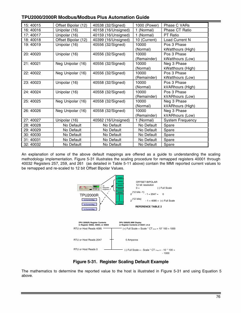
TPU2000/2000R Modbus/Modbus Plus Automation Guide
76
15: 40015 Offset Bipolar (12) 40538 (32/Signed) 1000 (Power) Phase C VARs16: 40016 Unipolar (16) 40158 (16/Unsigned) 1 (Normal) Phase CT Ratio17: 40017 Unipolar (16) 40159 (16/Unsigned) 1 (Normal) PT Ratio18: 40018 Offset Bipolar (12) 40399 (16/Unsigned) 10 (Current) Load Current N19: 40019 Unipolar (16) 40556 (32/Signed) 10000
(Normal)Pos 3 PhasekWatthours (High)
20: 40020 Unipolar (16) 40556 (32/Signed) 10000(Remainder)
Pos 3 PhasekWatthours (Low)
21: 40021 Neg Unipolar (16) 40556 (32/Signed) 10000(Normal)
Neg 3 PhasekWatthours (High)
22: 40022 Neg Unipolar (16) 40556 (32/Signed) 10000(Remainder)
Pos 3 PhasekWatthours (Low)
23: 40023 Unipolar (16) 40558 (32/Signed) 10000(Normal)
Pos 3 PhasekVARhours (High)
24: 40024 Unipolar (16) 40558 (32/Signed) 10000(Remainder)
Pos 3 PhasekVARhours (Low)
25: 40025 Neg Unipolar (16) 40558 (32/Signed) 10000(Normal)
Neg 3 PhasekVARhours (High)
26: 40026 Neg Unipolar (16) 40558 (32/Signed) 10000(Remainder)
Neg 3 PhasekVARhours (Low)
27: 40027 Unipolar (16) 40562 (16/Unsigned) 1 (Normal) System Frequency28: 40028 No Default No Default No Default Spare29: 40029 No Default No Default No Default Spare30: 40030 No Default No Default No Default Spare31: 40031 No Default No Default No Default Spare32: 40032 No Default No Default No Default Spare
An explanation of some of the above default mappings are offered as a guide to understanding the scalingmethodology implementation. Figure 5-31 illustrates the scaling procedure for remapped registers 40001 through40032 Registers 257, 259, and 261 (as detailed in Table 5-11 above) contain the MMI reported current values tobe remapped and re-scaled to 12 bit Offset Bipolar Values.
E
C
NORMALF A I LPICKUP
RECLOSER OUT
SYSTEM RESET
TIMEINSTANTANEOUS
FREQUENCYNEGATIVE SEQUENCE
TARGET RESET
S T A T U S TARGETS
ABCN
DPU2000R
Network
PartnerV1.0
TPU2000R
32Mappable Registers
400001
400002
400003
400004
400005
400032
Ia Current Mag.
Ib Current Mag.
Ic Current Mag.
OFFSET BIPOLAR12 bit resolution0 = (-) Full Scale
(12 bits -1)2 - 1 = 2047 = 0
(12 bits)2 - 1 = 4095 = (+) Full Scale
REFERENCE TABLE 2
(+) Full Scale = Scale * CT phase = 10* 100 = 1000
(-) Full Scale = - Scale * CT Phase = - 10 * 100 = - 1000
0 Amperes
RTU or Host Reads 0
RTU or Host Reads 2047
RTU or Host Reads 4095
DPU 2000(R) Register Contentsin Register 40002, 40003, or 40004
DPU 2000(R) MMI Displayor Register Contents of 40257, et al
Figure 5-31. Register Scaling Default Example
The mathematics to determine the reported value to the host is illustrated in Figure 5-31 and using Equation 5above.
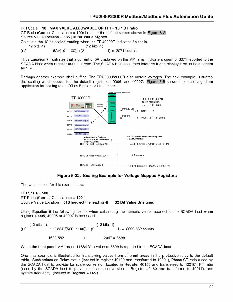
TPU2000/2000R Modbus/Modbus Plus Automation Guide
77
Full Scale = 10 MAX VALUE ALLOWABLE ON FPI = 10 * CT ratio.CT Ratio (Current Calculation) = 100:1 (as per the default screen shown in Figure 8-2)Source Value Location = 385 [16 Bit Value SignedCalculate the 12 bit scaled reading when the TPU2000R indicates 5A for Ia. (12 bits -1) (12 bits -1)(( 2 * 5A)/(10 * 100)) +(2 - 1) = 3071 counts.
Thus Equation 7 illustrates that a current of 5A displayed on the MMI shall indicate a count of 3071 reported to theSCADA Host when register 40002 is read. The SCADA host shall then interpret it and display it on its host screenas 5 A.
Perhaps another example shall suffice. The TPU2000/2000R also meters voltages. The next example illustratesthe scaling which occurs for the default registers, 40006, and 40007. Figure 8-8 shows the scale algorithmapplication for scaling to an Offset Bipolar 12 bit number.
Change Register Configuration
E
C
NORMALFAILPICKUP
RECLOSER OUT
SYSTEM RESET
TIMEINSTANTANEOUSFREQUENCY
NEGATIVE SEQUENCE
TARGET RESET
STATUS TARGETS
ABCN
DPU2000R
NetworkPartner
V 1 . 0
TPU2000R32Mappable Registers
400001 . . .400005
400006
400007
400032
Va Voltage Mag. Hi
VbVoltage Mag. Hi
40265
40266
40268
40269
40271
40272
Vc Voltage Mag. Hi
Va Voltage Mag . Lo
VbVoltage Mag. Lo
Vc Voltage Mag. Lo
OFFSET BIPOLAR12 bit resolution0 = (-) Full Scale
(12 bits -1)2 - 1 = 2047 = 0
(12 bits)2 - 1 = 4095 = (+) Full Scale
(+) Full Scale = 50000 V = FS * PT
(-) Full Scale = - 50000 V = FS * PT
0 Amperes
RTU or Host Reads 0
RTU or Host Reads 2047
RTU or Host Reads 4095
TPU 2000/2000R Metered Value reportedto the MMI SCREEN
Value stored in Registers 40005, 40006,and 40007 read bythe SCADA Host.
Figure 5-32. Scaling Example for Voltage Mapped Registers
The values used for this example are:
Full Scale = 500PT Ratio (Current Calculation) = 100:1Source Value Location = 513 [neglect the leading 4] 32 Bit Value Unsigned
Using Equation 6 the following results when calculating the numeric value reported to the SCADA host whenregister 40005, 40006 or 40007 is accessed.
(12 bits -1) (12 bits -1)(( 2 * 11884)/(500 * 100)) + (2 - 1) = 3699.562 counts
1622.562 + 2047 = 3699
When the front panel MMI reads 11884 V, a value of 3699 is reported to the SCADA host.
One final example is illustrated for transferring values from different areas in the protective relay to the defaulttable. Such values as Relay status (located in register 40129 and transferred to 40001), Phase CT ratio (used bythe SCADA host to provide for scale conversion located in Register 40158 and transferred to 40016), PT ratio(used by the SCADA host to provide for scale conversion in Register 40160 and transferred to 40017), andsystem frequency (located in Register 40027).
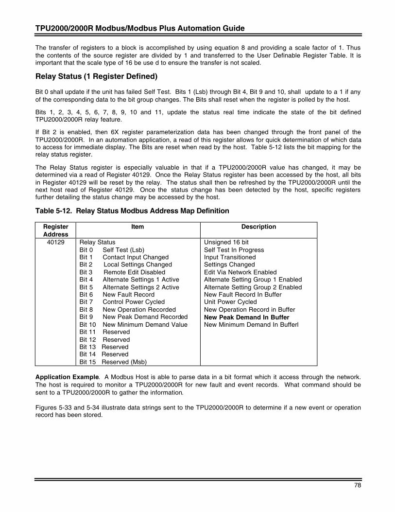
TPU2000/2000R Modbus/Modbus Plus Automation Guide
78
The transfer of registers to a block is accomplished by using equation 8 and providing a scale factor of 1. Thusthe contents of the source register are divided by 1 and transferred to the User Definable Register Table. It isimportant that the scale type of 16 be use d to ensure the transfer is not scaled.
Relay Status (1 Register Defined)
Bit 0 shall update if the unit has failed Self Test. Bits 1 (Lsb) through Bit 4, Bit 9 and 10, shall update to a 1 if anyof the corresponding data to the bit group changes. The Bits shall reset when the register is polled by the host.
Bits 1, 2, 3, 4, 5, 6, 7, 8, 9, 10 and 11, update the status real time indicate the state of the bit definedTPU2000/2000R relay feature.
If Bit 2 is enabled, then 6X register parameterization data has been changed through the front panel of theTPU2000/2000R. In an automation application, a read of this register allows for quick determination of which datato access for immediate display. The Bits are reset when read by the host. Table 5-12 lists the bit mapping for therelay status register.
The Relay Status register is especially valuable in that if a TPU2000/2000R value has changed, it may bedetermined via a read of Register 40129. Once the Relay Status register has been accessed by the host, all bitsin Register 40129 will be reset by the relay. The status shall then be refreshed by the TPU2000/2000R until thenext host read of Register 40129. Once the status change has been detected by the host, specific registersfurther detailing the status change may be accessed by the host.
Table 5-12. Relay Status Modbus Address Map Definition
RegisterAddress
Item Description
40129 Relay StatusBit 0 Self Test (Lsb)Bit 1 Contact Input ChangedBit 2 Local Settings ChangedBit 3 Remote Edit DisabledBit 4 Alternate Settings 1 ActiveBit 5 Alternate Settings 2 ActiveBit 6 New Fault RecordBit 7 Control Power CycledBit 8 New Operation RecordedBit 9 New Peak Demand RecordedBit 10 New Minimum Demand ValueBit 11 ReservedBit 12 ReservedBit 13 ReservedBit 14 ReservedBit 15 Reserved (Msb)
Unsigned 16 bitSelf Test In ProgressInput TransitionedSettings ChangedEdit Via Network EnabledAlternate Setting Group 1 EnabledAlternate Setting Group 2 EnabledNew Fault Record In BufferUnit Power CycledNew Operation Record in BufferNew Peak Demand In BufferNew Minimum Demand In Bufferl
Application Example. A Modbus Host is able to parse data in a bit format which it access through the network.The host is required to monitor a TPU2000/2000R for new fault and event records. What command should besent to a TPU2000/2000R to gather the information.
Figures 5-33 and 5-34 illustrate data strings sent to the TPU2000/2000R to determine if a new event or operationrecord has been stored.
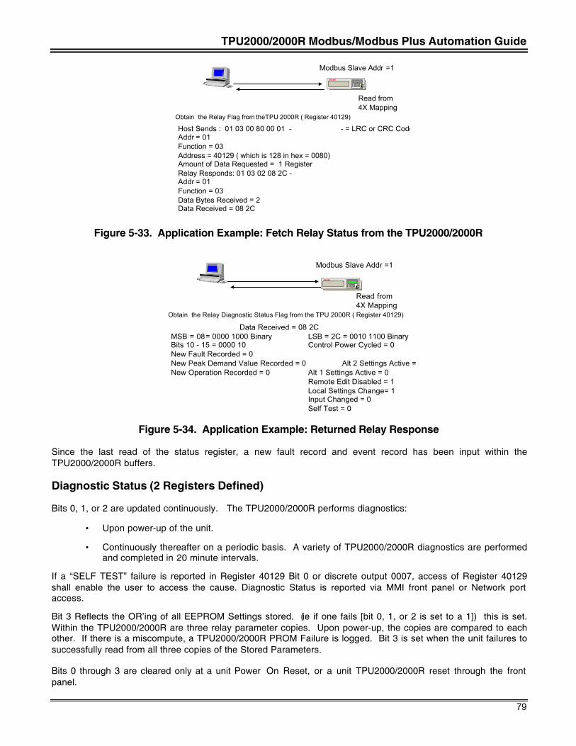
TPU2000/2000R Modbus/Modbus Plus Automation Guide
79
Modbus Slave Addr =1
Read from 4X Mapping
Obtain the Relay Flag from theTPU 2000R ( Register 40129)
Host Sends : 01 03 00 80 00 01 - - = LRC or CRC CodeAddr = 01Function = 03Address = 40129 ( which is 128 in hex = 0080)Amount of Data Requested = 1 RegisterRelay Responds: 01 03 02 08 2C -Addr = 01Function = 03Data Bytes Received = 2Data Received = 08 2C
EC
Figure 5-33. Application Example: Fetch Relay Status from the TPU2000/2000R
Modbus Slave Addr =1
Read from 4X Mapping
Obtain the Relay Diagnostic Status Flag from the TPU 2000R ( Register 40129)
Data Received = 08 2CMSB = 08= 0000 1000 Binary LSB = 2C = 0010 1100 BinaryBits 10 - 15 = 0000 10 Control Power Cycled = 0New Fault Recorded = 0New Peak Demand Value Recorded = 0 Alt 2 Settings Active = 1New Operation Recorded = 0 Alt 1 Settings Active = 0
Remote Edit Disabled = 1Local Settings Change= 1Input Changed = 0Self Test = 0
EC
Figure 5-34. Application Example: Returned Relay Response
Since the last read of the status register, a new fault record and event record has been input within theTPU2000/2000R buffers.
Diagnostic Status (2 Registers Defined)
Bits 0, 1, or 2 are updated continuously. The TPU2000/2000R performs diagnostics:
• Upon power-up of the unit.
• Continuously thereafter on a periodic basis. A variety of TPU2000/2000R diagnostics are performedand completed in 20 minute intervals.
If a “SELF TEST” failure is reported in Register 40129 Bit 0 or discrete output 0007, access of Register 40129shall enable the user to access the cause. Diagnostic Status is reported via MMI front panel or Network portaccess.
Bit 3 Reflects the OR’ing of all EEPROM Settings stored. (ie if one fails [bit 0, 1, or 2 is set to a 1]) this is set.Within the TPU2000/2000R are three relay parameter copies. Upon power-up, the copies are compared to eachother. If there is a miscompute, a TPU2000/2000R PROM Failure is logged. Bit 3 is set when the unit failures tosuccessfully read from all three copies of the Stored Parameters.
Bits 0 through 3 are cleared only at a unit Power On Reset, or a unit TPU2000/2000R reset through the frontpanel.
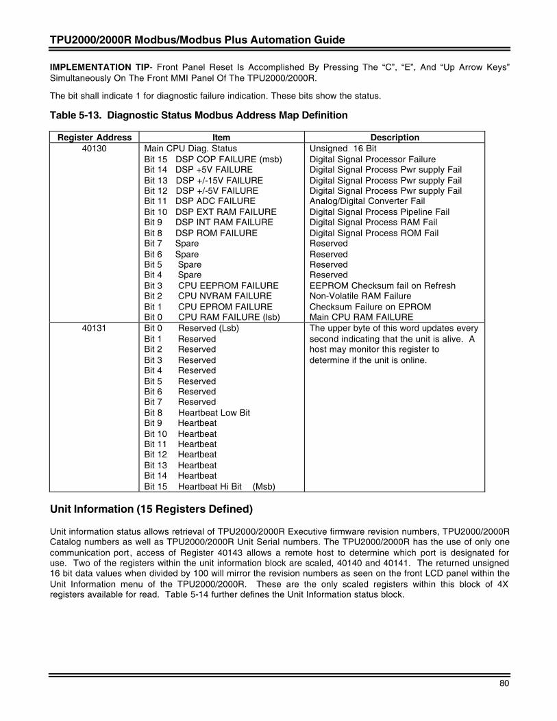
TPU2000/2000R Modbus/Modbus Plus Automation Guide
80
IMPLEMENTATION TIP- Front Panel Reset Is Accomplished By Pressing The “C”, “E”, And “Up Arrow Keys”Simultaneously On The Front MMI Panel Of The TPU2000/2000R.
The bit shall indicate 1 for diagnostic failure indication. These bits show the status.
Table 5-13. Diagnostic Status Modbus Address Map Definition
Register Address Item Description40130 Main CPU Diag. Status
Bit 15 DSP COP FAILURE (msb)Bit 14 DSP +5V FAILUREBit 13 DSP +/-15V FAILUREBit 12 DSP +/-5V FAILUREBit 11 DSP ADC FAILUREBit 10 DSP EXT RAM FAILUREBit 9 DSP INT RAM FAILUREBit 8 DSP ROM FAILUREBit 7 SpareBit 6 SpareBit 5 SpareBit 4 SpareBit 3 CPU EEPROM FAILUREBit 2 CPU NVRAM FAILUREBit 1 CPU EPROM FAILUREBit 0 CPU RAM FAILURE (lsb)
Unsigned 16 BitDigital Signal Processor FailureDigital Signal Process Pwr supply FailDigital Signal Process Pwr supply FailDigital Signal Process Pwr supply FailAnalog/Digital Converter FailDigital Signal Process Pipeline FailDigital Signal Process RAM FailDigital Signal Process ROM FailReservedReservedReservedReservedEEPROM Checksum fail on RefreshNon-Volatile RAM FailureChecksum Failure on EPROMMain CPU RAM FAILURE
40131 Bit 0 Reserved (Lsb)Bit 1 ReservedBit 2 ReservedBit 3 ReservedBit 4 ReservedBit 5 ReservedBit 6 ReservedBit 7 ReservedBit 8 Heartbeat Low BitBit 9 HeartbeatBit 10 HeartbeatBit 11 HeartbeatBit 12 HeartbeatBit 13 HeartbeatBit 14 HeartbeatBit 15 Heartbeat Hi Bit (Msb)
The upper byte of this word updates everysecond indicating that the unit is alive. Ahost may monitor this register todetermine if the unit is online.
Unit Information (15 Registers Defined)
Unit information status allows retrieval of TPU2000/2000R Executive firmware revision numbers, TPU2000/2000RCatalog numbers as well as TPU2000/2000R Unit Serial numbers. The TPU2000/2000R has the use of only onecommunication port, access of Register 40143 allows a remote host to determine which port is designated foruse. Two of the registers within the unit information block are scaled, 40140 and 40141. The returned unsigned16 bit data values when divided by 100 will mirror the revision numbers as seen on the front LCD panel within theUnit Information menu of the TPU2000/2000R. These are the only scaled registers within this block of 4Xregisters available for read. Table 5-14 further defines the Unit Information status block.
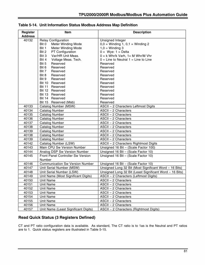
TPU2000/2000R Modbus/Modbus Plus Automation Guide
81
Table 5-14. Unit Information Status Modbus Address Map Definition
RegisterAddress
Item Description
40132 Relay ConfigurationBit 0 Meter Winding ModeBit 1 Meter Winding ModeBit 2 PT ConfigurationBit 3 Var/HR Unit Meas.Bit 4 Voltage Meas. Tech.Bit 5 ReservedBit 6 ReservedBit 7 ReservedBit 8 ReservedBit 9 ReservedBit 10 ReservedBit 11 ReservedBit 12 ReservedBit 13 ReservedBit 14 ReservedBit 15 Reserved (Msb)
Unsigned Integer0,0 = Winding 1, 0,1 = Winding 21,0 = Winding 30 = Wye: 1 = Delta0 = k Whr/k Varh, 1= M Whr/M Vhr0 = Line to Neutral 1 = Line to LineReservedReservedReservedReservedReservedReservedReservedReservedReservedReservedReserved
40133 Catalog Number (MSW) ASCII – 2 Characters Leftmost Digits40134 Catalog Number ASCII – 2 Characters40135 Catalog Number ASCII – 2 Characters40136 Catalog Number ASCII – 2 Characters40137 Catalog Number ASCII – 2 Characters40138 Catalog Number ASCII – 2 Characters40139 Catalog Number ASCII – 2 Characters40138 Catalog Number ASCII – 2 Characters40139 Catalog Number ASCII – 2 Characters40142 Catalog Number (LSW) ASCII – 2 Characters Rightmost Digits40143 Main CPU Sw Version Number Unsigned 16 Bit – (Scale Factor 100)40144 Analog DSP Sw Version Number Unsigned 16 Bit – (Scale Factor 10)40145 Front Panel Controller Sw Version
NumberUnsigned 16 Bit – (Scale Factor 10)
40146 Communication Sw Version Number Unsigned 16 Bit – (Scale Factor 10)40147 Unit Serial Number (MSW) Unsigned Long 32 Bit (Most Significant Word – 16 Bits)40148 Unit Serial Number (LSW) Unsigned Long 32 Bit (Least Significant Word – 16 Bits)40149 Unit Name (Most Significant Digits) ASCII – 2 Characters (Leftmost Digits)40150 Unit Name ASCII – 2 Characters40151 Unit Name ASCII – 2 Characters40152 Unit Name ASCII – 2 Characters40153 Unit Name ASCII – 2 Characters40154 Unit Name ASCII – 2 Characters40155 Unit Name ASCII – 2 Characters40156 Unit Name ASCII – 2 Characters40157 Unit Name (Least Significant Digits) ASCII – 2 Characters (Rightmost Digits)
Read Quick Status (3 Registers Defined)
CT and PT ratio configuration data is available. As standard, The CT ratio is to 1as is the Neutral and PT ratiosare to 1. Quick status registers are illustrated in Table 5-15.
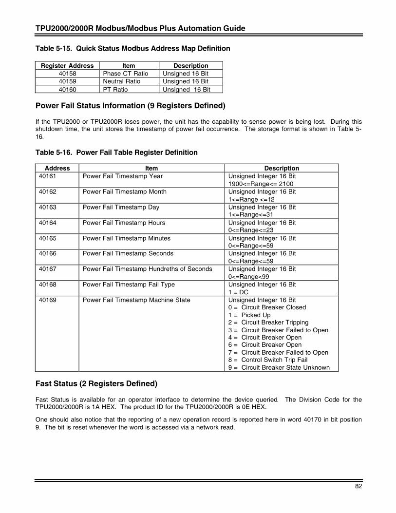
TPU2000/2000R Modbus/Modbus Plus Automation Guide
82
Table 5-15. Quick Status Modbus Address Map Definition
Register Address Item Description40158 Phase CT Ratio Unsigned 16 Bit40159 Neutral Ratio Unsigned 16 Bit40160 PT Ratio Unsigned 16 Bit
Power Fail Status Information (9 Registers Defined)
If the TPU2000 or TPU2000R loses power, the unit has the capability to sense power is being lost. During thisshutdown time, the unit stores the timestamp of power fail occurrence. The storage format is shown in Table 5-16.
Table 5-16. Power Fail Table Register Definition
Address Item Description40161 Power Fail Timestamp Year Unsigned Integer 16 Bit
1900<=Range<= 210040162 Power Fail Timestamp Month Unsigned Integer 16 Bit
1<=Range <=1240163 Power Fail Timestamp Day Unsigned Integer 16 Bit
1<=Range<=3140164 Power Fail Timestamp Hours Unsigned Integer 16 Bit
0<=Range<=2340165 Power Fail Timestamp Minutes Unsigned Integer 16 Bit
0<=Range<=5940166 Power Fail Timestamp Seconds Unsigned Integer 16 Bit
0<=Range<=5940167 Power Fail Timestamp Hundreths of Seconds Unsigned Integer 16 Bit
0<=Range<9940168 Power Fail Timestamp Fail Type Unsigned Integer 16 Bit
1 = DC40169 Power Fail Timestamp Machine State Unsigned Integer 16 Bit
0 = Circuit Breaker Closed1 = Picked Up2 = Circuit Breaker Tripping3 = Circuit Breaker Failed to Open4 = Circuit Breaker Open6 = Circuit Breaker Open7 = Circuit Breaker Failed to Open8 = Control Switch Trip Fail9 = Circuit Breaker State Unknown
Fast Status (2 Registers Defined)
Fast Status is available for an operator interface to determine the device queried. The Division Code for theTPU2000/2000R is 1A HEX. The product ID for the TPU2000/2000R is 0E HEX.
One should also notice that the reporting of a new operation record is reported here in word 40170 in bit position9. The bit is reset whenever the word is accessed via a network read.
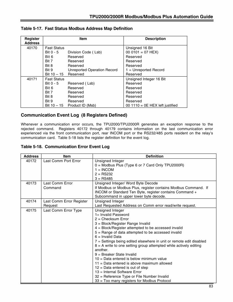
TPU2000/2000R Modbus/Modbus Plus Automation Guide
83
Table 5-17. Fast Status Modbus Address Map Definition
RegisterAddress
Item Description
40170 Fast StatusBit 0 - 5 Division Code ( Lsb)Bit 6 ReservedBit 7 ReservedBit 8 ReservedBit 9 Unreported Operation RecordBit 10 – 15 Reserved
Unsigned 16 Bit00 0101 = 07 HEX)ReservedReservedReserved1 = Unreported RecordReserved
40171 Fast StatusBit 0 - 5 Reserved ( Lsb)Bit 6 ReservedBit 7 ReservedBit 8 ReservedBit 9 ReservedBit 10 – 15 Product ID (Msb)
Unsigned Integer 16 BitReservedReservedReservedReservedReserved00 1110 = 0E HEX left justified
Communication Event Log (8 Registers Defined)
Whenever a communication error occurs, the TPU2000/TPU2000R generates an exception response to therejected command. Registers 40172 through 40179 contains information on the last communication errorexperienced via the front communication port, rear INCOM port or the RS232/485 ports resident on the relay’scommunication card. Table 5-18 lists the register definition for the event log.
Table 5-18. Communication Error Event Log
Address Item Definition40172 Last Comm Port Error Unsigned Integer
0 = Modbus Plus (Type 6 or 7 Card Only TPU2000R)1 = INCOM2 = RS2323 = RS485
40173 Last Comm ErrorCommand
Unsigned Integer/ Word Byte DecodeIf Modbus or Modbus Plus, register contains Modbus Command. IfINCOM or Standard Ten Byte, register contains Command +Subcommand in upper lower byte decode.
40174 Last Comm Error RegisterRequest
Unsigned IntegerLast Requested Address on Comm error read/write request.
40175 Last Comm Error Type Unsigned Integer1= Invalid Password2 = Checksum Error3 = Block/Register Range Invalid4 = Block/Register attempted to be accessed invalid5 = Range of data attempted to be accessed invalid6 = Invalid Data7 = Settings being edited elsewhere in unit or remote edit disabled8 = A write to one setting group attempted while actively editinganother.9 = Breaker State Invalid10 = Data entered is below minimum value11 = Data entered is above maximum allowed12 = Data entered is out of step13 = Internal Software Error32 = Reference Type or File Number Invalid33 = Too many registers for Modbus Protocol
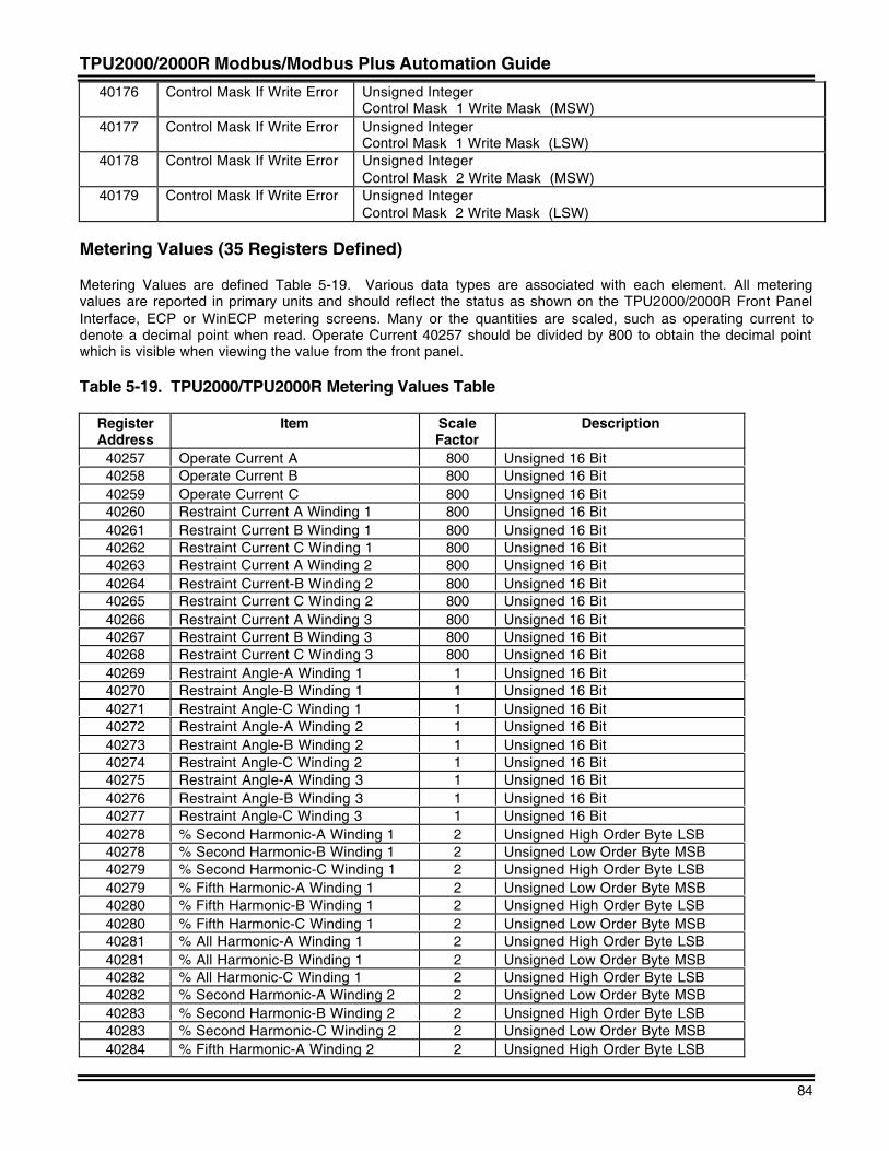
TPU2000/2000R Modbus/Modbus Plus Automation Guide
84
40176 Control Mask If Write Error Unsigned IntegerControl Mask 1 Write Mask (MSW)
40177 Control Mask If Write Error Unsigned IntegerControl Mask 1 Write Mask (LSW)
40178 Control Mask If Write Error Unsigned IntegerControl Mask 2 Write Mask (MSW)
40179 Control Mask If Write Error Unsigned IntegerControl Mask 2 Write Mask (LSW)
Metering Values (35 Registers Defined)
Metering Values are defined Table 5-19. Various data types are associated with each element. All meteringvalues are reported in primary units and should reflect the status as shown on the TPU2000/2000R Front PanelInterface, ECP or WinECP metering screens. Many or the quantities are scaled, such as operating current todenote a decimal point when read. Operate Current 40257 should be divided by 800 to obtain the decimal pointwhich is visible when viewing the value from the front panel.
Table 5-19. TPU2000/TPU2000R Metering Values Table
RegisterAddress
Item ScaleFactor
Description
40257 Operate Current A 800 Unsigned 16 Bit40258 Operate Current B 800 Unsigned 16 Bit40259 Operate Current C 800 Unsigned 16 Bit40260 Restraint Current A Winding 1 800 Unsigned 16 Bit40261 Restraint Current B Winding 1 800 Unsigned 16 Bit40262 Restraint Current C Winding 1 800 Unsigned 16 Bit40263 Restraint Current A Winding 2 800 Unsigned 16 Bit40264 Restraint Current-B Winding 2 800 Unsigned 16 Bit40265 Restraint Current C Winding 2 800 Unsigned 16 Bit40266 Restraint Current A Winding 3 800 Unsigned 16 Bit40267 Restraint Current B Winding 3 800 Unsigned 16 Bit40268 Restraint Current C Winding 3 800 Unsigned 16 Bit40269 Restraint Angle-A Winding 1 1 Unsigned 16 Bit40270 Restraint Angle-B Winding 1 1 Unsigned 16 Bit40271 Restraint Angle-C Winding 1 1 Unsigned 16 Bit40272 Restraint Angle-A Winding 2 1 Unsigned 16 Bit40273 Restraint Angle-B Winding 2 1 Unsigned 16 Bit40274 Restraint Angle-C Winding 2 1 Unsigned 16 Bit40275 Restraint Angle-A Winding 3 1 Unsigned 16 Bit40276 Restraint Angle-B Winding 3 1 Unsigned 16 Bit40277 Restraint Angle-C Winding 3 1 Unsigned 16 Bit40278 % Second Harmonic-A Winding 1 2 Unsigned High Order Byte LSB40278 % Second Harmonic-B Winding 1 2 Unsigned Low Order Byte MSB40279 % Second Harmonic-C Winding 1 2 Unsigned High Order Byte LSB40279 % Fifth Harmonic-A Winding 1 2 Unsigned Low Order Byte MSB40280 % Fifth Harmonic-B Winding 1 2 Unsigned High Order Byte LSB40280 % Fifth Harmonic-C Winding 1 2 Unsigned Low Order Byte MSB40281 % All Harmonic-A Winding 1 2 Unsigned High Order Byte LSB40281 % All Harmonic-B Winding 1 2 Unsigned Low Order Byte MSB40282 % All Harmonic-C Winding 1 2 Unsigned High Order Byte LSB40282 % Second Harmonic-A Winding 2 2 Unsigned Low Order Byte MSB40283 % Second Harmonic-B Winding 2 2 Unsigned High Order Byte LSB40283 % Second Harmonic-C Winding 2 2 Unsigned Low Order Byte MSB40284 % Fifth Harmonic-A Winding 2 2 Unsigned High Order Byte LSB
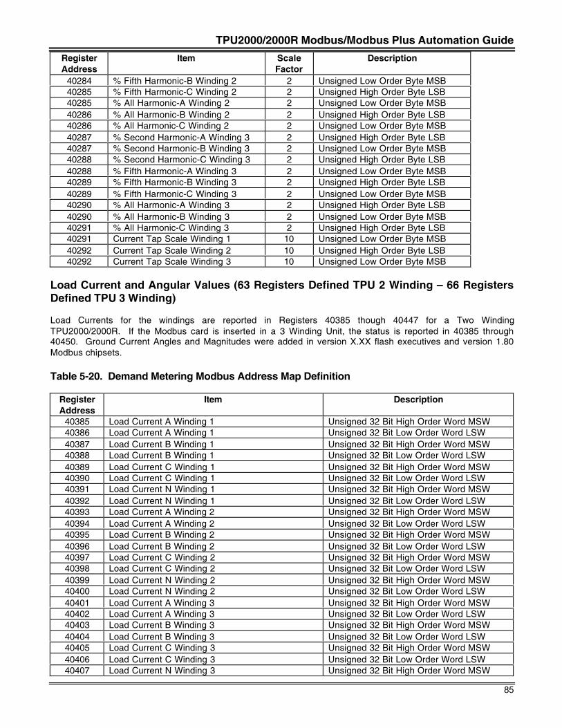
TPU2000/2000R Modbus/Modbus Plus Automation Guide
85
RegisterAddress
Item ScaleFactor
Description
40284 % Fifth Harmonic-B Winding 2 2 Unsigned Low Order Byte MSB40285 % Fifth Harmonic-C Winding 2 2 Unsigned High Order Byte LSB40285 % All Harmonic-A Winding 2 2 Unsigned Low Order Byte MSB40286 % All Harmonic-B Winding 2 2 Unsigned High Order Byte LSB40286 % All Harmonic-C Winding 2 2 Unsigned Low Order Byte MSB40287 % Second Harmonic-A Winding 3 2 Unsigned High Order Byte LSB40287 % Second Harmonic-B Winding 3 2 Unsigned Low Order Byte MSB40288 % Second Harmonic-C Winding 3 2 Unsigned High Order Byte LSB40288 % Fifth Harmonic-A Winding 3 2 Unsigned Low Order Byte MSB40289 % Fifth Harmonic-B Winding 3 2 Unsigned High Order Byte LSB40289 % Fifth Harmonic-C Winding 3 2 Unsigned Low Order Byte MSB40290 % All Harmonic-A Winding 3 2 Unsigned High Order Byte LSB40290 % All Harmonic-B Winding 3 2 Unsigned Low Order Byte MSB40291 % All Harmonic-C Winding 3 2 Unsigned High Order Byte LSB40291 Current Tap Scale Winding 1 10 Unsigned Low Order Byte MSB40292 Current Tap Scale Winding 2 10 Unsigned High Order Byte LSB40292 Current Tap Scale Winding 3 10 Unsigned Low Order Byte MSB
Load Current and Angular Values (63 Registers Defined TPU 2 Winding – 66 RegistersDefined TPU 3 Winding)
Load Currents for the windings are reported in Registers 40385 though 40447 for a Two WindingTPU2000/2000R. If the Modbus card is inserted in a 3 Winding Unit, the status is reported in 40385 through40450. Ground Current Angles and Magnitudes were added in version X.XX flash executives and version 1.80Modbus chipsets.
Table 5-20. Demand Metering Modbus Address Map Definition
RegisterAddress
Item Description
40385 Load Current A Winding 1 Unsigned 32 Bit High Order Word MSW40386 Load Current A Winding 1 Unsigned 32 Bit Low Order Word LSW40387 Load Current B Winding 1 Unsigned 32 Bit High Order Word MSW40388 Load Current B Winding 1 Unsigned 32 Bit Low Order Word LSW40389 Load Current C Winding 1 Unsigned 32 Bit High Order Word MSW40390 Load Current C Winding 1 Unsigned 32 Bit Low Order Word LSW40391 Load Current N Winding 1 Unsigned 32 Bit High Order Word MSW40392 Load Current N Winding 1 Unsigned 32 Bit Low Order Word LSW40393 Load Current A Winding 2 Unsigned 32 Bit High Order Word MSW40394 Load Current A Winding 2 Unsigned 32 Bit Low Order Word LSW40395 Load Current B Winding 2 Unsigned 32 Bit High Order Word MSW40396 Load Current B Winding 2 Unsigned 32 Bit Low Order Word LSW40397 Load Current C Winding 2 Unsigned 32 Bit High Order Word MSW40398 Load Current C Winding 2 Unsigned 32 Bit Low Order Word LSW40399 Load Current N Winding 2 Unsigned 32 Bit High Order Word MSW40400 Load Current N Winding 2 Unsigned 32 Bit Low Order Word LSW40401 Load Current A Winding 3 Unsigned 32 Bit High Order Word MSW40402 Load Current A Winding 3 Unsigned 32 Bit Low Order Word LSW40403 Load Current B Winding 3 Unsigned 32 Bit High Order Word MSW40404 Load Current B Winding 3 Unsigned 32 Bit Low Order Word LSW40405 Load Current C Winding 3 Unsigned 32 Bit High Order Word MSW40406 Load Current C Winding 3 Unsigned 32 Bit Low Order Word LSW40407 Load Current N Winding 3 Unsigned 32 Bit High Order Word MSW
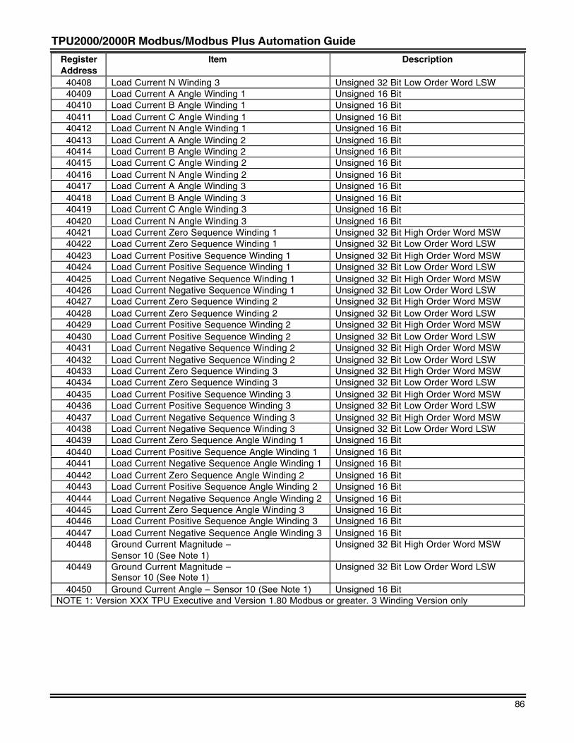
TPU2000/2000R Modbus/Modbus Plus Automation Guide
86
RegisterAddress
Item Description
40408 Load Current N Winding 3 Unsigned 32 Bit Low Order Word LSW40409 Load Current A Angle Winding 1 Unsigned 16 Bit40410 Load Current B Angle Winding 1 Unsigned 16 Bit40411 Load Current C Angle Winding 1 Unsigned 16 Bit40412 Load Current N Angle Winding 1 Unsigned 16 Bit40413 Load Current A Angle Winding 2 Unsigned 16 Bit40414 Load Current B Angle Winding 2 Unsigned 16 Bit40415 Load Current C Angle Winding 2 Unsigned 16 Bit40416 Load Current N Angle Winding 2 Unsigned 16 Bit40417 Load Current A Angle Winding 3 Unsigned 16 Bit40418 Load Current B Angle Winding 3 Unsigned 16 Bit40419 Load Current C Angle Winding 3 Unsigned 16 Bit40420 Load Current N Angle Winding 3 Unsigned 16 Bit40421 Load Current Zero Sequence Winding 1 Unsigned 32 Bit High Order Word MSW40422 Load Current Zero Sequence Winding 1 Unsigned 32 Bit Low Order Word LSW40423 Load Current Positive Sequence Winding 1 Unsigned 32 Bit High Order Word MSW40424 Load Current Positive Sequence Winding 1 Unsigned 32 Bit Low Order Word LSW40425 Load Current Negative Sequence Winding 1 Unsigned 32 Bit High Order Word MSW40426 Load Current Negative Sequence Winding 1 Unsigned 32 Bit Low Order Word LSW40427 Load Current Zero Sequence Winding 2 Unsigned 32 Bit High Order Word MSW40428 Load Current Zero Sequence Winding 2 Unsigned 32 Bit Low Order Word LSW40429 Load Current Positive Sequence Winding 2 Unsigned 32 Bit High Order Word MSW40430 Load Current Positive Sequence Winding 2 Unsigned 32 Bit Low Order Word LSW40431 Load Current Negative Sequence Winding 2 Unsigned 32 Bit High Order Word MSW40432 Load Current Negative Sequence Winding 2 Unsigned 32 Bit Low Order Word LSW40433 Load Current Zero Sequence Winding 3 Unsigned 32 Bit High Order Word MSW40434 Load Current Zero Sequence Winding 3 Unsigned 32 Bit Low Order Word LSW40435 Load Current Positive Sequence Winding 3 Unsigned 32 Bit High Order Word MSW40436 Load Current Positive Sequence Winding 3 Unsigned 32 Bit Low Order Word LSW40437 Load Current Negative Sequence Winding 3 Unsigned 32 Bit High Order Word MSW40438 Load Current Negative Sequence Winding 3 Unsigned 32 Bit Low Order Word LSW40439 Load Current Zero Sequence Angle Winding 1 Unsigned 16 Bit40440 Load Current Positive Sequence Angle Winding 1 Unsigned 16 Bit40441 Load Current Negative Sequence Angle Winding 1 Unsigned 16 Bit40442 Load Current Zero Sequence Angle Winding 2 Unsigned 16 Bit40443 Load Current Positive Sequence Angle Winding 2 Unsigned 16 Bit40444 Load Current Negative Sequence Angle Winding 2 Unsigned 16 Bit40445 Load Current Zero Sequence Angle Winding 3 Unsigned 16 Bit40446 Load Current Positive Sequence Angle Winding 3 Unsigned 16 Bit40447 Load Current Negative Sequence Angle Winding 3 Unsigned 16 Bit40448 Ground Current Magnitude –
Sensor 10 (See Note 1)Unsigned 32 Bit High Order Word MSW
40449 Ground Current Magnitude –Sensor 10 (See Note 1)
Unsigned 32 Bit Low Order Word LSW
40450 Ground Current Angle – Sensor 10 (See Note 1) Unsigned 16 BitNOTE 1: Version XXX TPU Executive and Version 1.80 Modbus or greater. 3 Winding Version only
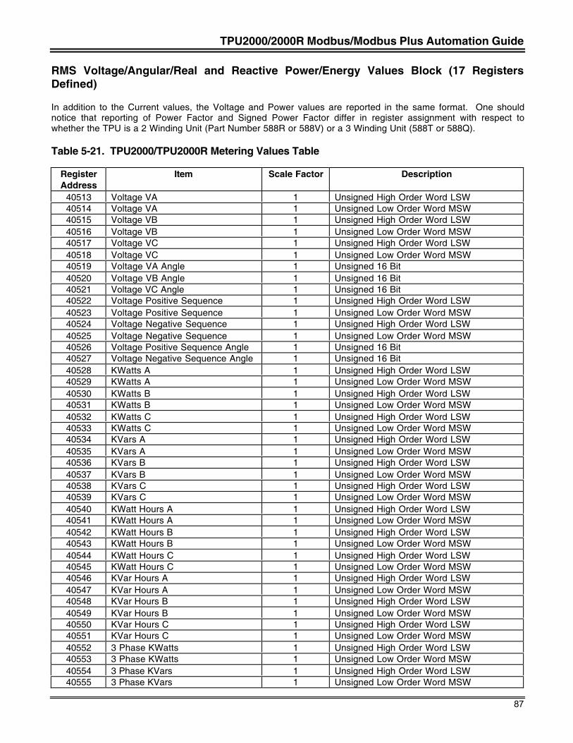
TPU2000/2000R Modbus/Modbus Plus Automation Guide
87
RMS Voltage/Angular/Real and Reactive Power/Energy Values Block (17 RegistersDefined)
In addition to the Current values, the Voltage and Power values are reported in the same format. One shouldnotice that reporting of Power Factor and Signed Power Factor differ in register assignment with respect towhether the TPU is a 2 Winding Unit (Part Number 588R or 588V) or a 3 Winding Unit (588T or 588Q).
Table 5-21. TPU2000/TPU2000R Metering Values Table
RegisterAddress
Item Scale Factor Description
40513 Voltage VA 1 Unsigned High Order Word LSW40514 Voltage VA 1 Unsigned Low Order Word MSW40515 Voltage VB 1 Unsigned High Order Word LSW40516 Voltage VB 1 Unsigned Low Order Word MSW40517 Voltage VC 1 Unsigned High Order Word LSW40518 Voltage VC 1 Unsigned Low Order Word MSW40519 Voltage VA Angle 1 Unsigned 16 Bit40520 Voltage VB Angle 1 Unsigned 16 Bit40521 Voltage VC Angle 1 Unsigned 16 Bit40522 Voltage Positive Sequence 1 Unsigned High Order Word LSW40523 Voltage Positive Sequence 1 Unsigned Low Order Word MSW40524 Voltage Negative Sequence 1 Unsigned High Order Word LSW40525 Voltage Negative Sequence 1 Unsigned Low Order Word MSW40526 Voltage Positive Sequence Angle 1 Unsigned 16 Bit40527 Voltage Negative Sequence Angle 1 Unsigned 16 Bit40528 KWatts A 1 Unsigned High Order Word LSW40529 KWatts A 1 Unsigned Low Order Word MSW40530 KWatts B 1 Unsigned High Order Word LSW40531 KWatts B 1 Unsigned Low Order Word MSW40532 KWatts C 1 Unsigned High Order Word LSW40533 KWatts C 1 Unsigned Low Order Word MSW40534 KVars A 1 Unsigned High Order Word LSW40535 KVars A 1 Unsigned Low Order Word MSW40536 KVars B 1 Unsigned High Order Word LSW40537 KVars B 1 Unsigned Low Order Word MSW40538 KVars C 1 Unsigned High Order Word LSW40539 KVars C 1 Unsigned Low Order Word MSW40540 KWatt Hours A 1 Unsigned High Order Word LSW40541 KWatt Hours A 1 Unsigned Low Order Word MSW40542 KWatt Hours B 1 Unsigned High Order Word LSW40543 KWatt Hours B 1 Unsigned Low Order Word MSW40544 KWatt Hours C 1 Unsigned High Order Word LSW40545 KWatt Hours C 1 Unsigned Low Order Word MSW40546 KVar Hours A 1 Unsigned High Order Word LSW40547 KVar Hours A 1 Unsigned Low Order Word MSW40548 KVar Hours B 1 Unsigned High Order Word LSW40549 KVar Hours B 1 Unsigned Low Order Word MSW40550 KVar Hours C 1 Unsigned High Order Word LSW40551 KVar Hours C 1 Unsigned Low Order Word MSW40552 3 Phase KWatts 1 Unsigned High Order Word LSW40553 3 Phase KWatts 1 Unsigned Low Order Word MSW40554 3 Phase KVars 1 Unsigned High Order Word LSW40555 3 Phase KVars 1 Unsigned Low Order Word MSW
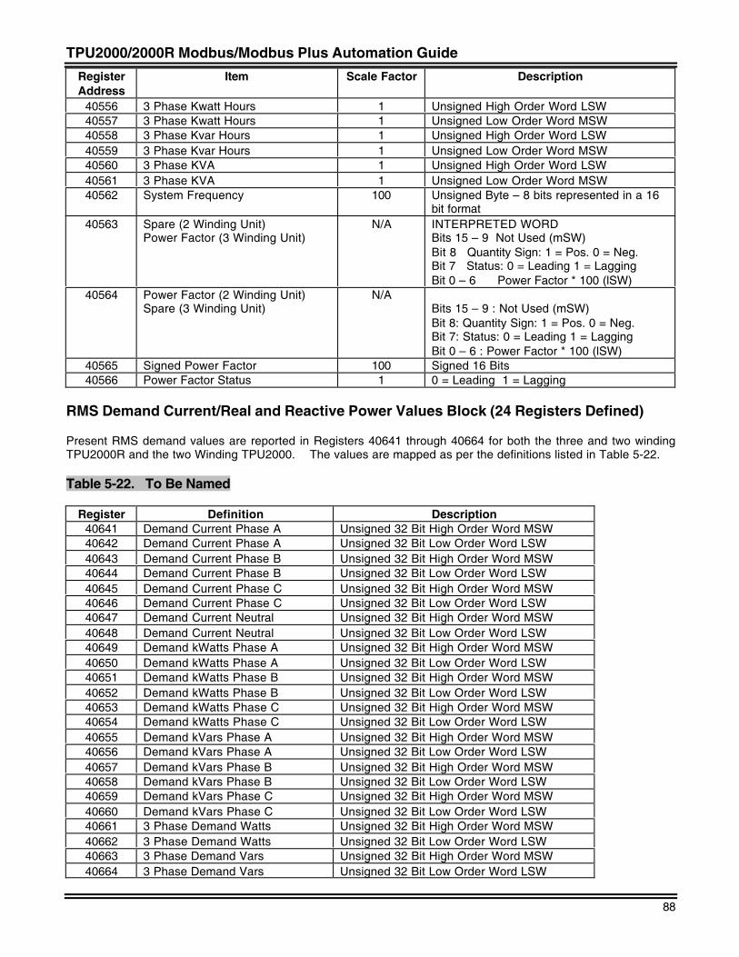
TPU2000/2000R Modbus/Modbus Plus Automation Guide
88
RegisterAddress
Item Scale Factor Description
40556 3 Phase Kwatt Hours 1 Unsigned High Order Word LSW40557 3 Phase Kwatt Hours 1 Unsigned Low Order Word MSW40558 3 Phase Kvar Hours 1 Unsigned High Order Word LSW40559 3 Phase Kvar Hours 1 Unsigned Low Order Word MSW40560 3 Phase KVA 1 Unsigned High Order Word LSW40561 3 Phase KVA 1 Unsigned Low Order Word MSW40562 System Frequency 100 Unsigned Byte – 8 bits represented in a 16
bit format40563 Spare (2 Winding Unit)
Power Factor (3 Winding Unit)N/A INTERPRETED WORD
Bits 15 – 9 Not Used (mSW)Bit 8 Quantity Sign: 1 = Pos. 0 = Neg.Bit 7 Status: 0 = Leading 1 = LaggingBit 0 – 6 Power Factor * 100 (lSW)
40564 Power Factor (2 Winding Unit)Spare (3 Winding Unit)
N/ABits 15 – 9 : Not Used (mSW)Bit 8: Quantity Sign: 1 = Pos. 0 = Neg.Bit 7: Status: 0 = Leading 1 = LaggingBit 0 – 6 : Power Factor * 100 (lSW)
40565 Signed Power Factor 100 Signed 16 Bits40566 Power Factor Status 1 0 = Leading 1 = Lagging
RMS Demand Current/Real and Reactive Power Values Block (24 Registers Defined)
Present RMS demand values are reported in Registers 40641 through 40664 for both the three and two windingTPU2000R and the two Winding TPU2000. The values are mapped as per the definitions listed in Table 5-22.
Table 5-22. To Be Named
Register Definition Description40641 Demand Current Phase A Unsigned 32 Bit High Order Word MSW40642 Demand Current Phase A Unsigned 32 Bit Low Order Word LSW40643 Demand Current Phase B Unsigned 32 Bit High Order Word MSW40644 Demand Current Phase B Unsigned 32 Bit Low Order Word LSW40645 Demand Current Phase C Unsigned 32 Bit High Order Word MSW40646 Demand Current Phase C Unsigned 32 Bit Low Order Word LSW40647 Demand Current Neutral Unsigned 32 Bit High Order Word MSW40648 Demand Current Neutral Unsigned 32 Bit Low Order Word LSW40649 Demand kWatts Phase A Unsigned 32 Bit High Order Word MSW40650 Demand kWatts Phase A Unsigned 32 Bit Low Order Word LSW40651 Demand kWatts Phase B Unsigned 32 Bit High Order Word MSW40652 Demand kWatts Phase B Unsigned 32 Bit Low Order Word LSW40653 Demand kWatts Phase C Unsigned 32 Bit High Order Word MSW40654 Demand kWatts Phase C Unsigned 32 Bit Low Order Word LSW40655 Demand kVars Phase A Unsigned 32 Bit High Order Word MSW40656 Demand kVars Phase A Unsigned 32 Bit Low Order Word LSW40657 Demand kVars Phase B Unsigned 32 Bit High Order Word MSW40658 Demand kVars Phase B Unsigned 32 Bit Low Order Word LSW40659 Demand kVars Phase C Unsigned 32 Bit High Order Word MSW40660 Demand kVars Phase C Unsigned 32 Bit Low Order Word LSW40661 3 Phase Demand Watts Unsigned 32 Bit High Order Word MSW40662 3 Phase Demand Watts Unsigned 32 Bit Low Order Word LSW40663 3 Phase Demand Vars Unsigned 32 Bit High Order Word MSW40664 3 Phase Demand Vars Unsigned 32 Bit Low Order Word LSW
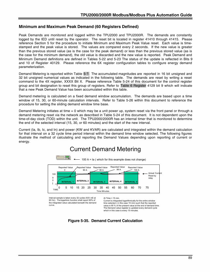
TPU2000/2000R Modbus/Modbus Plus Automation Guide
89
Minimum and Maximum Peak Demand (60 Registers Defined)
Peak Demands are monitored and logged within the TPU2000 and TPU2000R. The demands are constantlylogged by the IED until reset by the operator. The reset bit is located in register 41410 through 41415. Pleasereference Section 5 for the procedure to initiate Minimum and Maximum Peak Value reset. Each value is time-stamped and the peak value is stored. The values are compared every 2 seconds. If the new value is greaterthan the previous stored value (as is the case for the peak demand) or less than the previous stored value (as isthe case for the minimum demand), the old value is discarded and the new value is reported. Peak Demand andMinimum Demand definitions are defined in Tables 5-22 and 5-23 The status of the update is reflected in Bits 9and 10 of Register 40129. Please reference the 6X register configuration tables to configure energy demandparameterization.
Demand Metering is reported within Table 5-?. The accumulated magnitudes are reported in 16 bit unsigned and32 bit unsigned numerical values as indicated in the following table. The demands are reset by writing a resetcommand to the 4X register, XXXX Bit X. Please reference Table 5-24 of this document for the control registergroup and bit designation to reset this group of registers. Refer to Table 6 Register 4129 bit 9 which will indicatethat a new Peak Demand Value has been accumulated within this table.
Demand metering is calculated on a fixed demand window accumulation. The demands are based upon a timewindow of 15, 30, or 60-minute calculation intervals. Refer to Table 5-26 within this document to reference theprocedure for setting the sliding demand window time base.
Demand Metering initiates at time = 0 which may be a unit power up, system reset via the front panel or through ademand metering reset via the network as described in Table 5-24 of this document. It is not dependent upon thetime-of-day clock (TOD) within the unit. The TPU2000/2000R has an internal timer that is monitored to determinethe end of the selected interval (15, 30, or 60 minutes) and the start of the new interval.
Current (Ia, Ib, Ic, and In) and power (KW and KVAR) are calculated and integrated within the demand calculationfor that interval on a 32 cycle time period interval within the demand time window selected. The following figuresillustrate the method of calculating and reporting the Demand Values depending upon reporting of current orenergy.
Current Demand Metering100 A = Ia ( which for this example does not change)
Time Minutes
I0 5 10 15 20 25 30 35 40 45 50 55 60 70 75
90
At Time = 15 min.Current is integrated logarithmically for the entire window time selected ( in this case 15 min) such that the reported value is 90 % of the present value at the end of demand time.The Demand value register is updated every demand cyclewhich in this case is every 15 minutes.
100
INTERVAL 1
TIME
Actual CurrentRead by relay
INTERVAL 2 INTERVAL 3
Interval sample is taken every 32 cycles (533 mS at60 Hz). The logaritmic function shall report 90% of the integrated value calculated beneath the demand curve.
Reported Value 0
Reported Value 90 A
Reported Value 98 A
INTERVAL 4 INTERVAL 5
Reported Value 99 A
Reported Value 100 A
EC
Figure 5-35. Demand Current Calculation
TPU2000/2000R Modbus/Modbus Plus Automation Guide
90
Energy Demand Metering1000 KW ( which for this example does not change)
Time Minutes
KW0 5 10 15 20 25 30 35 40 45 50 55 60 70 75
At Time window end= 15 min,(selected demand interval), 30 minutes,45 minutes,...the relay updates the demand register with the calculated energy value.
If the relay is reset prior to the demand window time elapsing, the time shall reset to 0.
1000
TIME
ActualEnergyCalculated by relay.INTERVAL 1
Interval sample is taken every 1/15 th of the selected demand interval (in this case every minute).The logaritmic function shall report 90% of the integrated value calculated beneath the demand curve.
Reported Value 0
Reported Value 900 KW
Reported Value 900 KW
Reported Value 900 KW
Reported Value 900 KW
900
INTERVAL 2 INTERVAL 3 INTERVAL 4
EC
Figure 5-36. Energy Demand Calculation
Figures 5-35 and 5-36 illustrate the energy and current calculation methods and data reported when accessed viathe network. To simplify the explanation, the current and energy has been kept constant. This example illustratesa calculation based upon a window size of 15 minute demand intervals.
Table 5-23. Peak Demand Register Map for the TPU2000R and TPU2000
RegisterAddress
Item Description
40769 Peak Demand Current Phase A Unsigned 32 Bit High Order Word MSW40770 Peak Demand Current Phase A Unsigned 32 Bit Low Order Word LSW40771 Peak Demand Current Phase A Year Most Significant Byte 8 Bits
00<= Range <= 9940771 Peak Demand Current Phase A Month Least Significant Byte 8 Bits
00<= Range <= 1240772 Peak Demand Current Phase A Day Most Significant Byte 8 Bits
00<= Range<= 3140772 Peak Demand Current Phase A Hour Most Significant Byte 8 Bits
00<= Range <= 2340773 Peak Demand Current Phase A Minute Most Significant Byte 8 Bits
00<= Range <= 5940773 Reserved Byte Reserved40774 Peak Demand Current Phase B Unsigned 32 Bit High Order Word MSW40775 Peak Demand Current Phase B Unsigned 32 Bit Low Order Word LSW40776 Peak Demand Current Phase B Year Most Significant Byte 8 Bits
00<= Range <= 9940776 Peak Demand Current Phase B Month Least Significant Byte 8 Bits
00<= Range <= 1240777 Peak Demand Current Phase B Day Most Significant Byte 8 Bits
00<= Range<= 3140777 Peak Demand Current Phase B Hour Most Significant Byte 8 Bits
00<= Range <= 2340778 Peak Demand Current Phase B Minute Most Significant Byte 8 Bits
00<= Range <= 5940778 Reserved Byte Reserved40779 Peak Demand Current Phase C Unsigned 32 Bit High Order Word MSW40780 Peak Demand Current Phase C Unsigned 32 Bit Low Order Word LSW40781 Peak Demand Current Phase C Year Most Significant Byte 8 Bits
TPU2000/2000R Modbus/Modbus Plus Automation Guide
91
RegisterAddress
Item Description
00<= Range <= 9940781 Peak Demand Current Phase C Month Least Significant Byte 8 Bits
00<= Range <= 1240782 Peak Demand Current Phase C Day Most Significant Byte 8 Bits
00<= Range<= 3140782 Peak Demand Current Phase C Hour Most Significant Byte 8 Bits
00<= Range <= 2340783 Peak Demand Current Phase C Minute Most Significant Byte 8 Bits
00<= Range <= 5940783 Reserved Byte Reserved40784 Peak Demand Current Neutral Unsigned 32 Bit High Order Word MSW40785 Peak Demand Current Neutral Unsigned 32 Bit Low Order Word LSW40786 Peak Demand Current Neutral Year Most Significant Byte 8 Bits
00<= Range <= 9940786 Peak Demand Current Neutral Month Least Significant Byte 8 Bits
00<= Range <= 1240787 Peak Demand Current Neutral Day Most Significant Byte 8 Bits
00<= Range<= 3140787 Peak Demand Current Neutral Hour Most Significant Byte 8 Bits
00<= Range <= 2340788 Peak Demand Current Neutral Minute Most Significant Byte 8 Bits
00<= Range <= 5940788 Reserved Byte Reserved40789 Kwatt Hours (Phase A) Peak Demand Signed 32 Bit High Order Word MSW40790 Kwatt Hours (Phase A) Peak Demand Signed 32 Bit Low Order Word LSW40791 Peak Demand Kwatt Hours (Phase A)
YearMost Significant Byte 8 Bits00<= Range <= 99
40791 Peak Demand Kwatt Hours (Phase A)Month
Least Significant Byte 8 Bits00<= Range <= 12
40792 Peak Demand Kwatt Hours (Phase A)Day
Most Significant Byte 8 Bits00<= Range<= 31
40792 Peak Demand Kwatt Hours (Phase A)Hour
Most Significant Byte 8 Bits00<= Range <= 23
40793 Peak Demand Kwatt Hours (Phase A)Minute
Most Significant Byte 8 Bits00<= Range <= 59
40793 Reserved Byte Reserved40794 Kwatt Hours (Phase B) Peak Demand Signed 32 Bit High Order Word MSW40795 Kwatt Hours (Phase B) Peak Demand Signed 32 Bit Low Order Word LSW40796 Peak Demand Kwatt Hours (Phase B)
YearMost Significant Byte 8 Bits00<= Range <= 99
40796 Peak Demand Kwatt Hours (Phase B)Month
Least Significant Byte 8 Bits00<= Range <= 12
40797 Peak Demand Kwatt Hours (Phase B)Day
Most Significant Byte 8 Bits00<= Range<= 31
40797 Peak Demand Kwatt Hours (Phase B)Hour
Most Significant Byte 8 Bits00<= Range <= 23
40798 Peak Demand Kwatt Hours (Phase B)Minute
Most Significant Byte 8 Bits00<= Range <= 59
40798 Reserved Byte Reserved40799 Kwatt Hours (Phase C) Peak Demand Signed 32 Bit High Order Word MSW40800 Kwatt Hours (Phase C) Peak Demand Signed 32 Bit Low Order Word LSW40801 Peak Demand Kwatt Hours (Phase C)
YearMost Significant Byte 8 Bits00<= Range <= 99
40801 Peak Demand Kwatt Hours (Phase C) Least Significant Byte 8 Bits
TPU2000/2000R Modbus/Modbus Plus Automation Guide
92
RegisterAddress
Item Description
Month 00<= Range <= 1240802 Peak Demand Kwatt Hours (Phase C)
DayMost Significant Byte 8 Bits00<= Range<= 31
40802 Peak Demand Kwatt Hours (Phase C)Hour
Most Significant Byte 8 Bits00<= Range <= 23
40803 Peak Demand Kwatt Hours (Phase C)Minute
Most Significant Byte 8 Bits00<= Range <= 59
40803 Reserved Byte Reserved40804 Kwatt Hours (3 Phase) Peak Demand Signed 32 Bit High Order Word MSW40805 Kwatt Hours (3 Phase) Peak Demand Signed 32 Bit Low Order Word LSW40806 Peak Demand Kwatt Hours (3 Phase)
YearMost Significant Byte 8 Bits00<= Range <= 99
40806 Peak Demand Kwatt Hours (3 Phase)Month
Least Significant Byte 8 Bits00<= Range <= 12
40807 Peak Demand Kwatt Hours (3 Phase)Day
Most Significant Byte 8 Bits00<= Range<= 31
40807 Peak Demand Kwatt Hours (3 Phase)Hour
Most Significant Byte 8 Bits00<= Range <= 23
40808 Peak Demand Kwatt Hours (3 Phase)Minute
Most Significant Byte 8 Bits00<= Range <= 59
40808 Reserved Byte Reserved40809 KVAR Hours (Phase A) Peak Demand Signed 32 Bit High Order Word MSW40810 KVAR Hours (Phase A) Peak Demand Signed 32 Bit Low Order Word LSW40811 Peak Demand KVAR Hours (Phase A)
YearMost Significant Byte 8 Bits00<= Range <= 99
40811 Peak Demand KVAR Hours (Phase A)Month
Least Significant Byte 8 Bits00<= Range <= 12
40812 Peak Demand KVAR Hours (Phase A)Day
Most Significant Byte 8 Bits00<= Range<= 31
40812 Peak Demand KVAR Hours (Phase A)Hour
Most Significant Byte 8 Bits00<= Range <= 23
40813 Peak Demand KVAR Hours (Phase A)Minute
Most Significant Byte 8 Bits00<= Range <= 59
40813 Reserved Byte Reserved40814 KVAR Hours (Phase B) Peak Demand Signed 32 Bit High Order Word MSW40815 KVAR Hours (Phase B) Peak Demand Signed 32 Bit Low Order Word LSW40816 Peak Demand KVAR Hours (Phase B)
YearMost Significant Byte 8 Bits00<= Range <= 99
40816 Peak Demand KVAR Hours (Phase B)Month
Least Significant Byte 8 Bits00<= Range <= 12
40817 Peak Demand KVAR Hours (Phase B)Day
Most Significant Byte 8 Bits00<= Range<= 31
40817 Peak Demand KVAR Hours (Phase B)Hour
Most Significant Byte 8 Bits00<= Range <= 23
40818 Peak Demand KVAR Hours (Phase B)Minute
Most Significant Byte 8 Bits00<= Range <= 59
40818 Reserved Byte Reserved40819 KVAR Hours (Phase C) Peak Demand Signed 32 Bit High Order Word MSW40820 KVAR Hours (Phase C) Peak Demand Signed 32 Bit Low Order Word LSW40821 Peak Demand KVAR Hours (Phase C)
YearMost Significant Byte 8 Bits00<= Range <= 99
40821 Peak Demand KVAR Hours (Phase C)Month
Least Significant Byte 8 Bits00<= Range <= 12
40822 Peak Demand KVAR Hours (Phase C) Most Significant Byte 8 Bits
TPU2000/2000R Modbus/Modbus Plus Automation Guide
93
RegisterAddress
Item Description
Day 00<= Range<= 3140822 Peak Demand KVAR Hours (Phase C)
HourMost Significant Byte 8 Bits00<= Range <= 23
40823 Peak Demand KVAR Hours (Phase C)Minute
Most Significant Byte 8 Bits00<= Range <= 59
40823 Reserved Byte Reserved40824 KVAR Hours (3 Phase) Peak Demand Signed 32 Bit High Order Word MSW40825 KVAR Hours (3 Phase) Peak Demand Signed 32 Bit Low Order Word LSW40826 Peak Demand KVAR Hours (3 Phase)
YearMost Significant Byte 8 Bits00<= Range <= 99
40826 Peak Demand KVAR Hours (3 Phase)Month
Least Significant Byte 8 Bits00<= Range <= 12
40827 Peak Demand KVAR Hours (3 Phase)Day
Most Significant Byte 8 Bits00<= Range<= 31
40827 Peak Demand KVAR Hours (3 Phase)Hour
Most Significant Byte 8 Bits00<= Range <= 23
40828 Peak Demand KVAR Hours (3 Phase)Minute
Most Significant Byte 8 Bits00<= Range <= 59
40828 Reserved Byte Reserved
The minimum demand table is as follows:
Table 5-24. Minimum Demand Register Map for the TPU2000R and TPU2000
RegisterAddress
Item Description
40897 Minimum Demand Current Phase A Unsigned 32 Bit High Order Word MSW40898 Minimum Demand Current Phase A Unsigned 32 Bit Low Order Word LSW40899 Minimum Demand Current Phase A Year Most Significant Byte 8 Bits
00<= Range <= 9940899 Minimum Demand Current Phase A Month Least Significant Byte 8 Bits
00<= Range <= 1240900 Minimum Demand Current Phase A Day Most Significant Byte 8 Bits
00<= Range<= 3140900 Minimum Demand Current Phase A Hour Most Significant Byte 8 Bits
00<= Range <= 2340901 Minimum Demand Current Phase A Minute Most Significant Byte 8 Bits
00<= Range <= 5940901 Reserved Byte Reserved40902 Minimum Demand Current Phase B Unsigned 32 Bit High Order Word MSW40903 Minimum Demand Current Phase B Unsigned 32 Bit Low Order Word LSW40904 Minimum Demand Current Phase B Year Most Significant Byte 8 Bits
00<= Range <= 9940904 Minimum Demand Current Phase B Month Least Significant Byte 8 Bits
00<= Range <= 1240905 Minimum Demand Current Phase B Day Most Significant Byte 8 Bits
00<= Range<= 3140905 Minimum Demand Current Phase B Hour Most Significant Byte 8 Bits
00<= Range <= 2340906 Minimum Demand Current Phase B Minute Most Significant Byte 8 Bits
00<= Range <= 5940906 Reserved Byte Reserved40907 Minimum Demand Current Phase C Unsigned 32 Bit High Order Word MSW40908 Minimum Demand Current Phase C Unsigned 32 Bit Low Order Word LSW
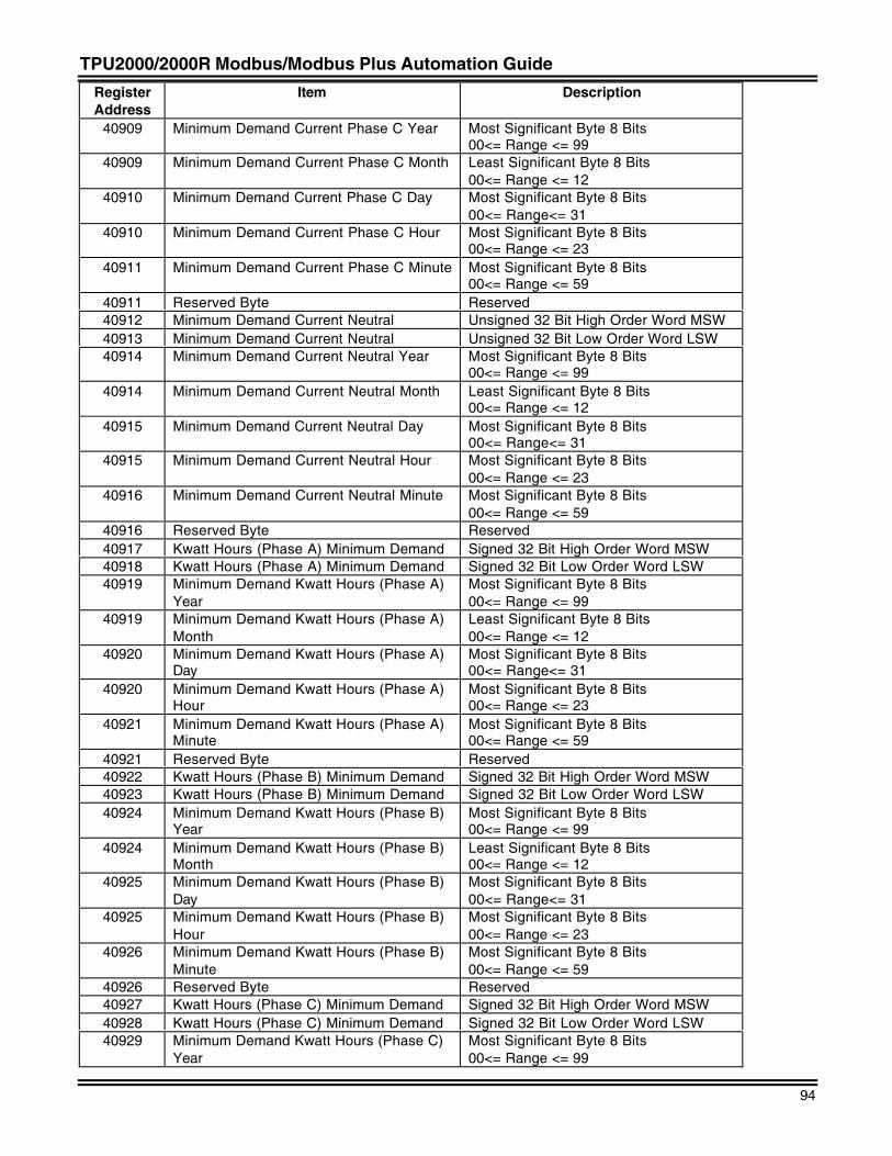
TPU2000/2000R Modbus/Modbus Plus Automation Guide
94
RegisterAddress
Item Description
40909 Minimum Demand Current Phase C Year Most Significant Byte 8 Bits00<= Range <= 99
40909 Minimum Demand Current Phase C Month Least Significant Byte 8 Bits00<= Range <= 12
40910 Minimum Demand Current Phase C Day Most Significant Byte 8 Bits00<= Range<= 31
40910 Minimum Demand Current Phase C Hour Most Significant Byte 8 Bits00<= Range <= 23
40911 Minimum Demand Current Phase C Minute Most Significant Byte 8 Bits00<= Range <= 59
40911 Reserved Byte Reserved40912 Minimum Demand Current Neutral Unsigned 32 Bit High Order Word MSW40913 Minimum Demand Current Neutral Unsigned 32 Bit Low Order Word LSW40914 Minimum Demand Current Neutral Year Most Significant Byte 8 Bits
00<= Range <= 9940914 Minimum Demand Current Neutral Month Least Significant Byte 8 Bits
00<= Range <= 1240915 Minimum Demand Current Neutral Day Most Significant Byte 8 Bits
00<= Range<= 3140915 Minimum Demand Current Neutral Hour Most Significant Byte 8 Bits
00<= Range <= 2340916 Minimum Demand Current Neutral Minute Most Significant Byte 8 Bits
00<= Range <= 5940916 Reserved Byte Reserved40917 Kwatt Hours (Phase A) Minimum Demand Signed 32 Bit High Order Word MSW40918 Kwatt Hours (Phase A) Minimum Demand Signed 32 Bit Low Order Word LSW40919 Minimum Demand Kwatt Hours (Phase A)
YearMost Significant Byte 8 Bits00<= Range <= 99
40919 Minimum Demand Kwatt Hours (Phase A)Month
Least Significant Byte 8 Bits00<= Range <= 12
40920 Minimum Demand Kwatt Hours (Phase A)Day
Most Significant Byte 8 Bits00<= Range<= 31
40920 Minimum Demand Kwatt Hours (Phase A)Hour
Most Significant Byte 8 Bits00<= Range <= 23
40921 Minimum Demand Kwatt Hours (Phase A)Minute
Most Significant Byte 8 Bits00<= Range <= 59
40921 Reserved Byte Reserved40922 Kwatt Hours (Phase B) Minimum Demand Signed 32 Bit High Order Word MSW40923 Kwatt Hours (Phase B) Minimum Demand Signed 32 Bit Low Order Word LSW40924 Minimum Demand Kwatt Hours (Phase B)
YearMost Significant Byte 8 Bits00<= Range <= 99
40924 Minimum Demand Kwatt Hours (Phase B)Month
Least Significant Byte 8 Bits00<= Range <= 12
40925 Minimum Demand Kwatt Hours (Phase B)Day
Most Significant Byte 8 Bits00<= Range<= 31
40925 Minimum Demand Kwatt Hours (Phase B)Hour
Most Significant Byte 8 Bits00<= Range <= 23
40926 Minimum Demand Kwatt Hours (Phase B)Minute
Most Significant Byte 8 Bits00<= Range <= 59
40926 Reserved Byte Reserved40927 Kwatt Hours (Phase C) Minimum Demand Signed 32 Bit High Order Word MSW40928 Kwatt Hours (Phase C) Minimum Demand Signed 32 Bit Low Order Word LSW40929 Minimum Demand Kwatt Hours (Phase C)
YearMost Significant Byte 8 Bits00<= Range <= 99
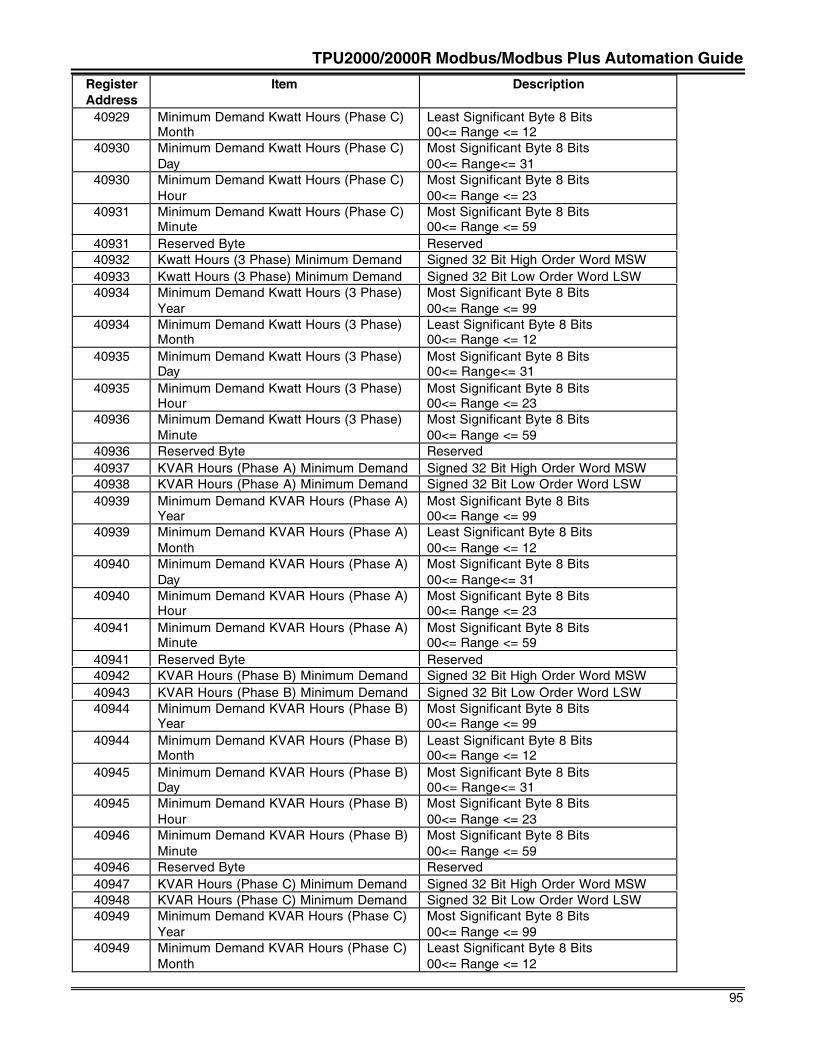
TPU2000/2000R Modbus/Modbus Plus Automation Guide
95
RegisterAddress
Item Description
40929 Minimum Demand Kwatt Hours (Phase C)Month
Least Significant Byte 8 Bits00<= Range <= 12
40930 Minimum Demand Kwatt Hours (Phase C)Day
Most Significant Byte 8 Bits00<= Range<= 31
40930 Minimum Demand Kwatt Hours (Phase C)Hour
Most Significant Byte 8 Bits00<= Range <= 23
40931 Minimum Demand Kwatt Hours (Phase C)Minute
Most Significant Byte 8 Bits00<= Range <= 59
40931 Reserved Byte Reserved40932 Kwatt Hours (3 Phase) Minimum Demand Signed 32 Bit High Order Word MSW40933 Kwatt Hours (3 Phase) Minimum Demand Signed 32 Bit Low Order Word LSW40934 Minimum Demand Kwatt Hours (3 Phase)
YearMost Significant Byte 8 Bits00<= Range <= 99
40934 Minimum Demand Kwatt Hours (3 Phase)Month
Least Significant Byte 8 Bits00<= Range <= 12
40935 Minimum Demand Kwatt Hours (3 Phase)Day
Most Significant Byte 8 Bits00<= Range<= 31
40935 Minimum Demand Kwatt Hours (3 Phase)Hour
Most Significant Byte 8 Bits00<= Range <= 23
40936 Minimum Demand Kwatt Hours (3 Phase)Minute
Most Significant Byte 8 Bits00<= Range <= 59
40936 Reserved Byte Reserved40937 KVAR Hours (Phase A) Minimum Demand Signed 32 Bit High Order Word MSW40938 KVAR Hours (Phase A) Minimum Demand Signed 32 Bit Low Order Word LSW40939 Minimum Demand KVAR Hours (Phase A)
YearMost Significant Byte 8 Bits00<= Range <= 99
40939 Minimum Demand KVAR Hours (Phase A)Month
Least Significant Byte 8 Bits00<= Range <= 12
40940 Minimum Demand KVAR Hours (Phase A)Day
Most Significant Byte 8 Bits00<= Range<= 31
40940 Minimum Demand KVAR Hours (Phase A)Hour
Most Significant Byte 8 Bits00<= Range <= 23
40941 Minimum Demand KVAR Hours (Phase A)Minute
Most Significant Byte 8 Bits00<= Range <= 59
40941 Reserved Byte Reserved40942 KVAR Hours (Phase B) Minimum Demand Signed 32 Bit High Order Word MSW40943 KVAR Hours (Phase B) Minimum Demand Signed 32 Bit Low Order Word LSW40944 Minimum Demand KVAR Hours (Phase B)
YearMost Significant Byte 8 Bits00<= Range <= 99
40944 Minimum Demand KVAR Hours (Phase B)Month
Least Significant Byte 8 Bits00<= Range <= 12
40945 Minimum Demand KVAR Hours (Phase B)Day
Most Significant Byte 8 Bits00<= Range<= 31
40945 Minimum Demand KVAR Hours (Phase B)Hour
Most Significant Byte 8 Bits00<= Range <= 23
40946 Minimum Demand KVAR Hours (Phase B)Minute
Most Significant Byte 8 Bits00<= Range <= 59
40946 Reserved Byte Reserved40947 KVAR Hours (Phase C) Minimum Demand Signed 32 Bit High Order Word MSW40948 KVAR Hours (Phase C) Minimum Demand Signed 32 Bit Low Order Word LSW40949 Minimum Demand KVAR Hours (Phase C)
YearMost Significant Byte 8 Bits00<= Range <= 99
40949 Minimum Demand KVAR Hours (Phase C)Month
Least Significant Byte 8 Bits00<= Range <= 12
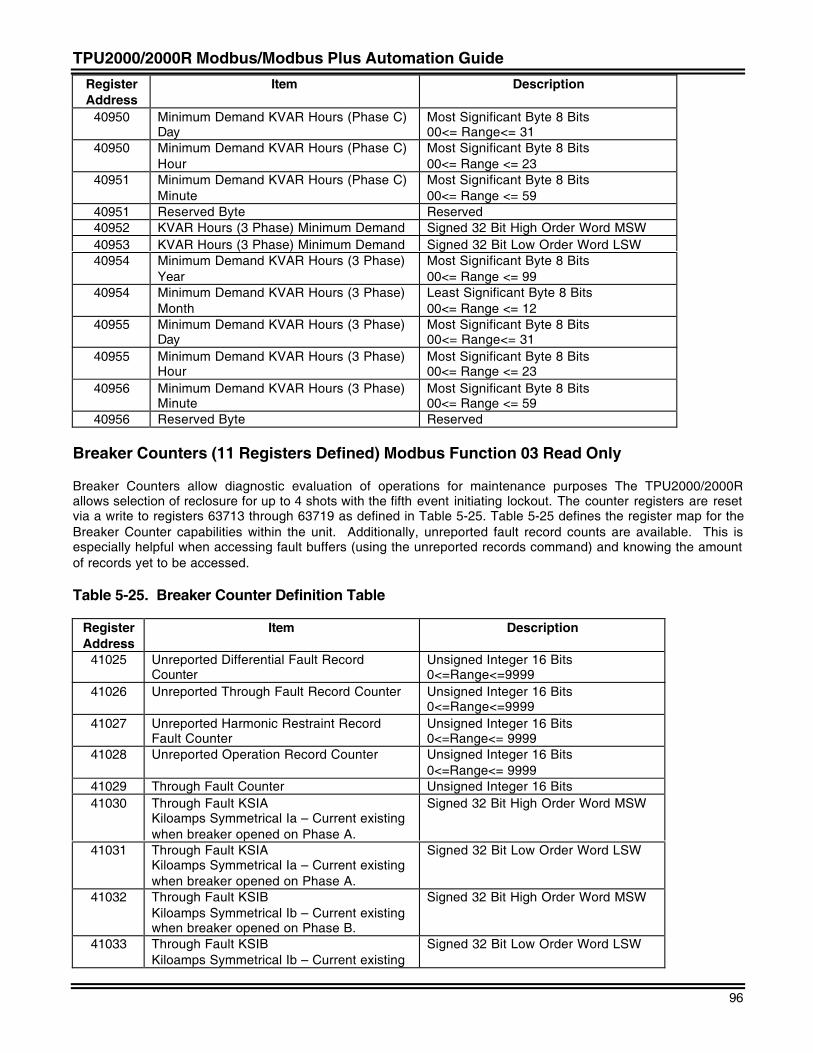
TPU2000/2000R Modbus/Modbus Plus Automation Guide
96
RegisterAddress
Item Description
40950 Minimum Demand KVAR Hours (Phase C)Day
Most Significant Byte 8 Bits00<= Range<= 31
40950 Minimum Demand KVAR Hours (Phase C)Hour
Most Significant Byte 8 Bits00<= Range <= 23
40951 Minimum Demand KVAR Hours (Phase C)Minute
Most Significant Byte 8 Bits00<= Range <= 59
40951 Reserved Byte Reserved40952 KVAR Hours (3 Phase) Minimum Demand Signed 32 Bit High Order Word MSW40953 KVAR Hours (3 Phase) Minimum Demand Signed 32 Bit Low Order Word LSW40954 Minimum Demand KVAR Hours (3 Phase)
YearMost Significant Byte 8 Bits00<= Range <= 99
40954 Minimum Demand KVAR Hours (3 Phase)Month
Least Significant Byte 8 Bits00<= Range <= 12
40955 Minimum Demand KVAR Hours (3 Phase)Day
Most Significant Byte 8 Bits00<= Range<= 31
40955 Minimum Demand KVAR Hours (3 Phase)Hour
Most Significant Byte 8 Bits00<= Range <= 23
40956 Minimum Demand KVAR Hours (3 Phase)Minute
Most Significant Byte 8 Bits00<= Range <= 59
40956 Reserved Byte Reserved
Breaker Counters (11 Registers Defined) Modbus Function 03 Read Only
Breaker Counters allow diagnostic evaluation of operations for maintenance purposes The TPU2000/2000Rallows selection of reclosure for up to 4 shots with the fifth event initiating lockout. The counter registers are resetvia a write to registers 63713 through 63719 as defined in Table 5-25. Table 5-25 defines the register map for theBreaker Counter capabilities within the unit. Additionally, unreported fault record counts are available. This isespecially helpful when accessing fault buffers (using the unreported records command) and knowing the amountof records yet to be accessed.
Table 5-25. Breaker Counter Definition Table
RegisterAddress
Item Description
41025 Unreported Differential Fault RecordCounter
Unsigned Integer 16 Bits0<=Range<=9999
41026 Unreported Through Fault Record Counter Unsigned Integer 16 Bits0<=Range<=9999
41027 Unreported Harmonic Restraint RecordFault Counter
Unsigned Integer 16 Bits0<=Range<= 9999
41028 Unreported Operation Record Counter Unsigned Integer 16 Bits0<=Range<= 9999
41029 Through Fault Counter Unsigned Integer 16 Bits41030 Through Fault KSIA
Kiloamps Symmetrical Ia – Current existingwhen breaker opened on Phase A.
Signed 32 Bit High Order Word MSW
41031 Through Fault KSIAKiloamps Symmetrical Ia – Current existingwhen breaker opened on Phase A.
Signed 32 Bit Low Order Word LSW
41032 Through Fault KSIBKiloamps Symmetrical Ib – Current existingwhen breaker opened on Phase B.
Signed 32 Bit High Order Word MSW
41033 Through Fault KSIBKiloamps Symmetrical Ib – Current existing
Signed 32 Bit Low Order Word LSW
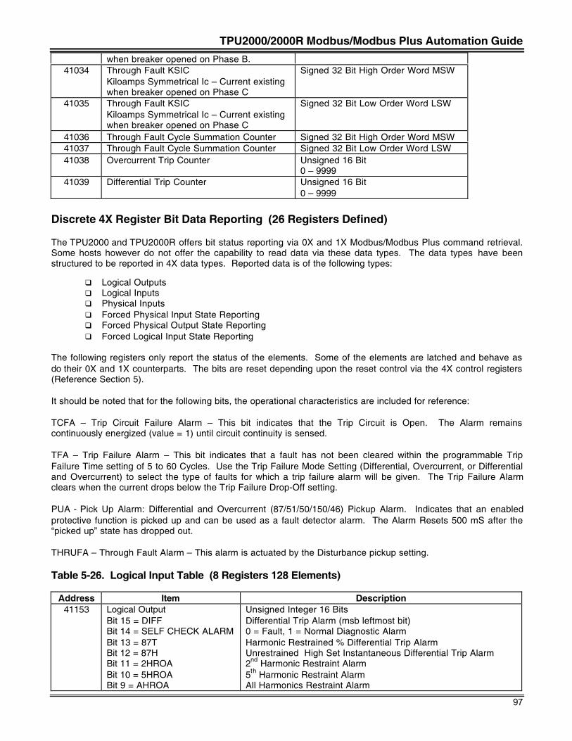
TPU2000/2000R Modbus/Modbus Plus Automation Guide
97
when breaker opened on Phase B.41034 Through Fault KSIC
Kiloamps Symmetrical Ic – Current existingwhen breaker opened on Phase C
Signed 32 Bit High Order Word MSW
41035 Through Fault KSICKiloamps Symmetrical Ic – Current existingwhen breaker opened on Phase C
Signed 32 Bit Low Order Word LSW
41036 Through Fault Cycle Summation Counter Signed 32 Bit High Order Word MSW41037 Through Fault Cycle Summation Counter Signed 32 Bit Low Order Word LSW41038 Overcurrent Trip Counter Unsigned 16 Bit
0 – 999941039 Differential Trip Counter Unsigned 16 Bit
0 – 9999
Discrete 4X Register Bit Data Reporting (26 Registers Defined)
The TPU2000 and TPU2000R offers bit status reporting via 0X and 1X Modbus/Modbus Plus command retrieval.Some hosts however do not offer the capability to read data via these data types. The data types have beenstructured to be reported in 4X data types. Reported data is of the following types:
q Logical Outputsq Logical Inputsq Physical Inputsq Forced Physical Input State Reportingq Forced Physical Output State Reportingq Forced Logical Input State Reporting
The following registers only report the status of the elements. Some of the elements are latched and behave asdo their 0X and 1X counterparts. The bits are reset depending upon the reset control via the 4X control registers(Reference Section 5).
It should be noted that for the following bits, the operational characteristics are included for reference:
TCFA – Trip Circuit Failure Alarm – This bit indicates that the Trip Circuit is Open. The Alarm remainscontinuously energized (value = 1) until circuit continuity is sensed.
TFA – Trip Failure Alarm – This bit indicates that a fault has not been cleared within the programmable TripFailure Time setting of 5 to 60 Cycles. Use the Trip Failure Mode Setting (Differential, Overcurrent, or Differentialand Overcurrent) to select the type of faults for which a trip failure alarm will be given. The Trip Failure Alarmclears when the current drops below the Trip Failure Drop-Off setting.
PUA - Pick Up Alarm: Differential and Overcurrent (87/51/50/150/46) Pickup Alarm. Indicates that an enabledprotective function is picked up and can be used as a fault detector alarm. The Alarm Resets 500 mS after the“picked up” state has dropped out.
THRUFA – Through Fault Alarm – This alarm is actuated by the Disturbance pickup setting.
Table 5-26. Logical Input Table (8 Registers 128 Elements)
Address Item Description41153 Logical Output
Bit 15 = DIFFBit 14 = SELF CHECK ALARMBit 13 = 87TBit 12 = 87HBit 11 = 2HROABit 10 = 5HROABit 9 = AHROA
Unsigned Integer 16 BitsDifferential Trip Alarm (msb leftmost bit)0 = Fault, 1 = Normal Diagnostic AlarmHarmonic Restrained % Differential Trip AlarmUnrestrained High Set Instantaneous Differential Trip Alarm2nd Harmonic Restraint Alarm5th Harmonic Restraint AlarmAll Harmonics Restraint Alarm
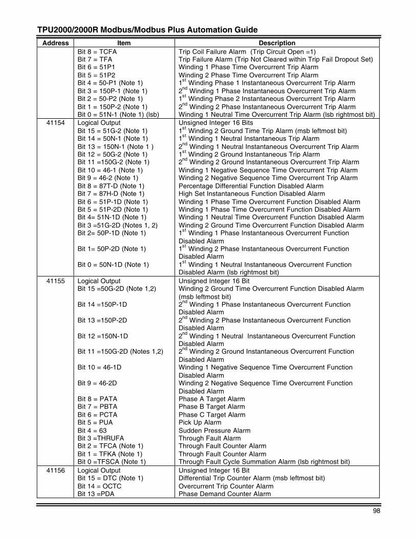
TPU2000/2000R Modbus/Modbus Plus Automation Guide
98
Address Item DescriptionBit 8 = TCFABit 7 = TFABit 6 = 51P1Bit 5 = 51P2Bit 4 = 50-P1 (Note 1)Bit 3 = 150P-1 (Note 1)Bit 2 = 50-P2 (Note 1)Bit 1 = 150P-2 (Note 1)Bit 0 = 51N-1 (Note 1) (lsb)
Trip Coil Failure Alarm (Trip Circuit Open =1)Trip Failure Alarm (Trip Not Cleared within Trip Fail Dropout Set)Winding 1 Phase Time Overcurrent Trip AlarmWinding 2 Phase Time Overcurrent Trip Alarm1st Winding Phase 1 Instantaneous Overcurrent Trip Alarm2nd Winding 1 Phase Instantaneous Overcurrent Trip Alarm1st Winding Phase 2 Instantaneous Overcurrent Trip Alarm2nd Winding 2 Phase Instantaneous Overcurrent Trip AlarmWinding 1 Neutral Time Overcurrent Trip Alarm (lsb rightmost bit)
41154 Logical OutputBit 15 = 51G-2 (Note 1)Bit 14 = 50N-1 (Note 1)Bit 13 = 150N-1 (Note 1 )Bit 12 = 50G-2 (Note 1)Bit 11 =150G-2 (Note 1)Bit 10 = 46-1 (Note 1)Bit 9 = 46-2 (Note 1)Bit 8 = 87T-D (Note 1)Bit 7 = 87H-D (Note 1)Bit 6 = 51P-1D (Note 1)Bit 5 = 51P-2D (Note 1)Bit 4= 51N-1D (Note 1)Bit 3 =51G-2D (Notes 1, 2)Bit 2= 50P-1D (Note 1)
Bit 1= 50P-2D (Note 1)
Bit 0 = 50N-1D (Note 1)
Unsigned Integer 16 Bits1st Winding 2 Ground Time Trip Alarm (msb leftmost bit)1st Winding 1 Neutral Instantaneous Trip Alarm2nd Winding 1 Neutral Instantaneous Overcurrent Trip Alarm1st Winding 2 Ground Instantaneous Trip Alarm2nd Winding 2 Ground Instantaneous Overcurrent Trip AlarmWinding 1 Negative Sequence Time Overcurrent Trip AlarmWinding 2 Negative Sequence Time Overcurrent Trip AlarmPercentage Differential Function Disabled AlarmHigh Set Instantaneous Function Disabled AlarmWinding 1 Phase Time Overcurrent Function Disabled AlarmWinding 1 Phase Time Overcurrent Function Disabled AlarmWinding 1 Neutral Time Overcurrent Function Disabled AlarmWinding 2 Ground Time Overcurrent Function Disabled Alarm1st Winding 1 Phase Instantaneous Overcurrent FunctionDisabled Alarm1st Winding 2 Phase Instantaneous Overcurrent FunctionDisabled Alarm1st Winding 1 Neutral Instantaneous Overcurrent FunctionDisabled Alarm (lsb rightmost bit)
41155 Logical OutputBit 15 =50G-2D (Note 1,2)
Bit 14 =150P-1D
Bit 13 =150P-2D
Bit 12 =150N-1D
Bit 11 =150G-2D (Notes 1,2)
Bit 10 = 46-1D
Bit 9 = 46-2D
Bit 8 = PATABit 7 = PBTABit 6 = PCTABit 5 = PUABit 4 = 63Bit 3 =THRUFABit 2 = TFCA (Note 1)Bit 1 = TFKA (Note 1)Bit 0 =TFSCA (Note 1)
Unsigned Integer 16 BitWinding 2 Ground Time Overcurrent Function Disabled Alarm(msb leftmost bit)2nd Winding 1 Phase Instantaneous Overcurrent FunctionDisabled Alarm2nd Winding 2 Phase Instantaneous Overcurrent FunctionDisabled Alarm2nd Winding 1 Neutral Instantaneous Overcurrent FunctionDisabled Alarm2nd Winding 2 Ground Instantaneous Overcurrent FunctionDisabled AlarmWinding 1 Negative Sequence Time Overcurrent FunctionDisabled AlarmWinding 2 Negative Sequence Time Overcurrent FunctionDisabled AlarmPhase A Target AlarmPhase B Target AlarmPhase C Target AlarmPick Up AlarmSudden Pressure AlarmThrough Fault AlarmThrough Fault Counter AlarmThrough Fault Counter AlarmThrough Fault Cycle Summation Alarm (lsb rightmost bit)
41156 Logical OutputBit 15 = DTC (Note 1)Bit 14 = OCTCBit 13 =PDA
Unsigned Integer 16 BitDifferential Trip Counter Alarm (msb leftmost bit)Overcurrent Trip Counter AlarmPhase Demand Counter Alarm
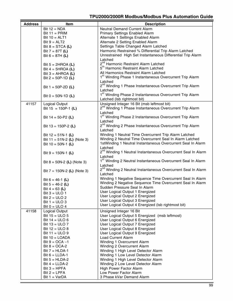
TPU2000/2000R Modbus/Modbus Plus Automation Guide
99
Address Item DescriptionBit 12 = NDABit 11 = PRIMBit 10 = ALT1Bit 9 = ALT2Bit 8 = STCA (L)Bit 7 = 87T (L)Bit 6 = 87H (L)
Bit 5 = 2HROA (L)Bit 4 = 5HROA (L)Bit 3 = AHROA (L)Bit 2 = 50P-1D (L)
Bit 1 = 50P-2D (L)
Bit 0 = 50N-1D (L)
Neutral Demand Current AlarmPrimary Settings Enabled AlarmAlternate 1 Settings Enabled AlarmAlternate 2 Setting Enabled AlarmSettings Table Changed Alarm LatchedHarmonic Restrained % Differential Trip Alarm LatchedUnrestrained High Set Instantaneous Differential Trip AlarmLatched2nd Harmonic Restraint Alarm Latched5th Harmonic Restraint Alarm LatchedAll Harmonics Restraint Alarm Latched1st Winding Phase 1 Instantaneous Overcurrent Trip AlarmLatched2nd Winding 1 Phase Instantaneous Overcurrent Trip AlarmLatched1st Winding Phase 2 Instantaneous Overcurrent Trip AlarmLatched (lsb rightmost bit)
41157 Logical OutputBit 15 = 150P-1 (L)
Bit 14 = 50-P2 (L)
Bit 13 = 150P-2 (L)
Bit 12 = 51N-1 (L)Bit 11 = 51N-2 (L) (Note 3)Bit 10 = 50N-1 (L)
Bit 9 = 150N-1 (L)
Bit 8 = 50N-2 (L) (Note 3)
Bit 7 = 150N-2 (L) (Note 3)
Bit 6 = 46-1 (L)Bit 5 = 46-2 (L)Bit 4 = 63 (L)Bit 3 = ULO 1Bit 2 = ULO 2Bit 1 = ULO 3Bit 0 = ULO 4
Unsigned Integer 16 Bit (msb leftmost bit)2nd Winding 1 Phase Instantaneous Overcurrent Trip AlarmLatched1st Winding Phase 2 Instantaneous Overcurrent Trip AlarmLatched2nd Winding 2 Phase Instantaneous Overcurrent Trip AlarmLatchedWinding 1 Neutral Time Overcurrent Trip Alarm LatchedWinding 2 Neutral Time Overcurrent Seal In Alarm Latched1stWinding 1 Neutral Instantaneous Overcurrent Seal In AlarmLatched2nd Winding 1 Neutral Instantaneous Overcurrent Seal In AlarmLatched1st Winding 2 Neutral Instantaneous Overcurrent Seal In AlarmLatched2nd Winding 2 Neutral Instantaneous Overcurrent Seal In AlarmLatchedWinding 1 Negative Sequence Time Overcurrent Seal In AlarmWinding 2 Negative Sequence Time Overcurrent Seal In AlarmSudden Pressure Seal In AlarmUser Logical Output 1 EnergizedUser Logical Output 2 EnergizedUser Logical Output 3 EnergizedUser Logical Output 4 Energized (lsb rightmost bit)
41158 Logical OutputBit 15 = ULO 5Bit 14 = ULO 6Bit 13 = ULO 7Bit 12 = ULO 8Bit 11 = ULO 9Bit 10 = LOADABit 9 = OCA –1Bit 8 = OCA-2Bit 7 = HLDA-1Bit 6 = LLDA-1Bit 5 = HLDA-2Bit 4 = LLDA-2Bit 3 = HPFABit 2 = LPFABit 1 = VarDA
Unsigned Integer 16 BitUser Logical Output 5 Energized (msb leftmost)User Logical Output 6 EnergizedUser Logical Output 7 EnergizedUser Logical Output 8 EnergizedUser Logical Output 9 EnergizedLoad Current AlarmWinding 1 Overcurrent AlarmWinding 2 Overcurrent AlarmWinding 1 High Level Detector AlarmWinding 1 Low Level Detector AlarmWinding 1 High Level Detector AlarmWinding 2 Low Level Detector AlarmHigh Power Factor AlarmLow Power Factor Alarm3 Phase kVar Demand Alarm
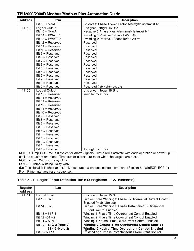
TPU2000/2000R Modbus/Modbus Plus Automation Guide
100
Address Item DescriptionBit 0 = PVarA Positive 3 Phase Power Factor Alarm(lsb rightmost bit)
41159 Logical OutputBit 15 = NvarABit 14 = PWATT1Bit 13 = PWATT2Bit 12 = ReservedBit 11 = ReservedBit 10 = ReservedBit 9 = ReservedBit 8 = ReservedBit 7 = ReservedBit 6 = ReservedBit 5 = ReservedBit 4 = ReservedBit 3 = ReservedBit 2 = ReservedBit 1 = ReservedBit 0 = Reserved
Unsigned Integer 16 BitsNegative 3 Phase Kvar Alarm(msb leftmost bit)Pwinding 1 Positive 3Phase kWatt AlarmPwinding 2 Positive 3Phase kWatt AlarmReservedReservedReservedReservedReservedReservedReservedReservedReservedReservedReservedReservedReserved (lsb rightmost bit)
41160 Logical OutputBit 15 = ReservedBit 14 = ReservedBit 13 = ReservedBit 12 = ReservedBit 11 = ReservedBit 10 = ReservedBit 9 = ReservedBit 8 = ReservedBit 7 = ReservedBit 6 = ReservedBit 5 = ReservedBit 4 = ReservedBit 3 = ReservedBit 2 = ReservedBit 1 = ReservedBit 0 = Reserved
Unsigned Integer 16 Bits(msb leftmost bit)
(lsb rightmost bit)NOTE 1: Drop Out Time is 3 cycles for Alarm Signals. The alarms activate with each operation or power-upuntil the counters are reset. The counter alarms are reset when the targets are reset.NOTE 2: Two Winding Relay OnlyNOTE 3: Three Winding Relay Only(L): This signal is latched and is only reset upon a protocol control command (Section 5), WinECP, ECP, orFront Panel Interface reset sequence.
Table 5-27. Logical Input Definition Table (8 Registers – 127 Elements)
RegisterAddress
Item Description
41161 Logical InputBit 15 = 87T
Bit 14 = 87H
Bit 13 = 51P-1Bit 12 =51P-2Bit 11 = 51N-1Bit 10 = 51G-2 (Note 2) 51N-2 (Note 3)Bit 9 = 50P-1
Unsigned Integer 16 BitTwo or Three Winding 3 Phase % Differential Current ControlEnabled (msb leftmost)Two or Three Winding 3 Phase Instantaneous DifferentialCurrent Control EnabledWinding 1 Phase Time Overcurrent Control EnabledWinding 2 Phase Time Overcurrent Control EnabledWinding 1 Neutral Time Overcurrent Control EnabledWinding 2 Ground Time Overcurrent Control EnabledWinding 2 Neutral Time Overcurrent Control Enabled1st Winding 1 Phase Instantaneous Overcurrent Control
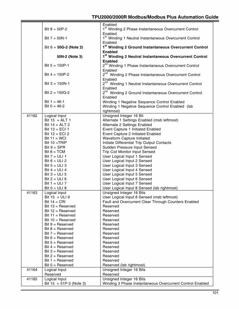
TPU2000/2000R Modbus/Modbus Plus Automation Guide
101
Bit 8 = 50P-2
Bit 7 = 50N-1
Bit 6 = 50G-2 (Note 2)
50N-2 (Note 3)
Bit 5 = 150P-1
Bit 4 = 150P-2
Bit 3 = 150N-1
Bit 2 = 150G-2
Bit 1 = 46-1Bit 0 = 46-2
Enabled1st Winding 2 Phase Instantaneous Overcurrent ControlEnabled1st Winding 1 Neutral Instantaneous Overcurrent ControlEnabled1st Winding 2 Ground Instantaneous Overcurrent ControlEnabled1st Winding 2 Neutral Instantaneous Overcurrent ControlEnabled2nd Winding 1 Phase Instantaneous Overcurrent ControlEnabled2nd Winding 2 Phase Instantaneous Overcurrent ControlEnabled2nd Winding 1 Neutral Instantaneous Overcurrent ControlEnabled2nd Winding 2 Ground Instantaneous Overcurrent ControlEnabledWinding 1 Negative Sequence Control EnabledWinding 1 Negative Sequence Control Enabled (lsbrightmost)
41162 Logical InputBit 15 = ALT 1Bit 14 = ALT 2Bit 13 = ECI 1Bit 12 = ECI 2Bit 11 = WCIBit 10 =TRIPBit 9 = SPRBit 8 = TCMBit 7 = ULI 1Bit 6 = ULI 2Bit 5 = ULI 3Bit 4 = ULI 4Bit 3 = ULI 5Bit 2 = ULI 6Bit 1 = ULI 7Bit 0 = ULI 8
Unsigned Integer 16 BitAlternate 1 Settings Enabled (msb leftmost)Alternate 2 Settings EnabledEvent Capture 1 Initiated EnabledEvent Capture 2 Initiated EnabledWaveform Capture InitiatedInitiate Differential Trip Output ContactsSudden Pressure Input SensedTrip Coil Monitor Input SensedUser Logical Input 1 SensedUser Logical Input 2 SensedUser Logical Input 3 SensedUser Logical Input 4 SensedUser Logical Input 5 SensedUser Logical Input 6 SensedUser Logical Input 7 SensedUser Logical Input 8 Sensed (lsb rightmost)
41163 Logical InputBit 15 = ULI 9Bit 14 = CRIBit 13 = ReservedBit 12 = ReservedBit 11 = ReservedBit 10 = ReservedBit 9 = ReservedBit 8 = ReservedBit 7 = ReservedBit 6 = ReservedBit 5 = ReservedBit 4 = ReservedBit 3 = ReservedBit 2 = ReservedBit 1 = ReservedBit 0 = Reserved
Unsigned Integer 16 BitsUser Logical Input 8 Sensed (msb leftmost)Fault and Overcurrent Clear Through Counters EnabledReservedReservedReservedReservedReservedReservedReservedReservedReservedReservedReservedReservedReservedReserved (lsb rightmost)
41164 Logical InputReserved
Unsigned Integer 16 BitsReserved
41165 Logical InputBit 15 = 51P-3 (Note 3)
Unsigned Integer 16 BitsWinding 3 Phase Instantaneous Overcurrent Control Enabled
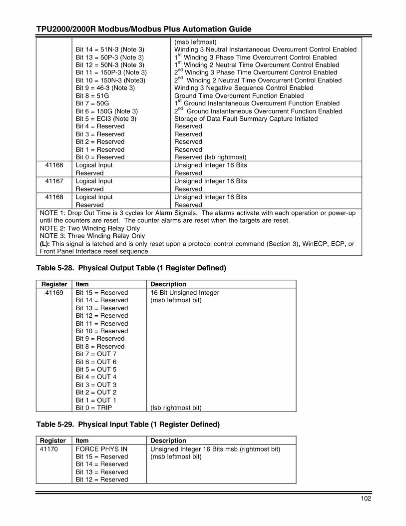
TPU2000/2000R Modbus/Modbus Plus Automation Guide
102
Bit 14 = 51N-3 (Note 3)Bit 13 = 50P-3 (Note 3)Bit 12 = 50N-3 (Note 3)Bit 11 = 150P-3 (Note 3)Bit 10 = 150N-3 (Note3)Bit 9 = 46-3 (Note 3)Bit 8 = 51GBit 7 = 50GBit 6 = 150G (Note 3)Bit 5 = ECI3 (Note 3)Bit 4 = ReservedBit 3 = ReservedBit 2 = ReservedBit 1 = ReservedBit 0 = Reserved
(msb leftmost)Winding 3 Neutral Instantaneous Overcurrent Control Enabled1st Winding 3 Phase Time Overcurrent Control Enabled1st Winding 2 Neutral Time Overcurrent Control Enabled2nd Winding 3 Phase Time Overcurrent Control Enabled2nd Winding 2 Neutral Time Overcurrent Control EnabledWinding 3 Negative Sequence Control EnabledGround Time Overcurrent Function Enabled1st Ground Instantaneous Overcurrent Function Enabled2nd Ground Instantaneous Overcurrent Function EnabledStorage of Data Fault Summary Capture InitiatedReservedReservedReservedReservedReserved (lsb rightmost)
41166 Logical InputReserved
Unsigned Integer 16 BitsReserved
41167 Logical InputReserved
Unsigned Integer 16 BitsReserved
41168 Logical InputReserved
Unsigned Integer 16 BitsReserved
NOTE 1: Drop Out Time is 3 cycles for Alarm Signals. The alarms activate with each operation or power-upuntil the counters are reset. The counter alarms are reset when the targets are reset.NOTE 2: Two Winding Relay OnlyNOTE 3: Three Winding Relay Only(L): This signal is latched and is only reset upon a protocol control command (Section 3), WinECP, ECP, orFront Panel Interface reset sequence.
Table 5-28. Physical Output Table (1 Register Defined)
Register Item Description41169 Bit 15 = Reserved
Bit 14 = ReservedBit 13 = ReservedBit 12 = ReservedBit 11 = ReservedBit 10 = ReservedBit 9 = ReservedBit 8 = ReservedBit 7 = OUT 7Bit 6 = OUT 6Bit 5 = OUT 5Bit 4 = OUT 4Bit 3 = OUT 3Bit 2 = OUT 2Bit 1 = OUT 1Bit 0 = TRIP
16 Bit Unsigned Integer(msb leftmost bit)
(lsb rightmost bit)
Table 5-29. Physical Input Table (1 Register Defined)
Register Item Description41170 FORCE PHYS IN
Bit 15 = ReservedBit 14 = ReservedBit 13 = ReservedBit 12 = Reserved
Unsigned Integer 16 Bits msb (rightmost bit)(msb leftmost bit)
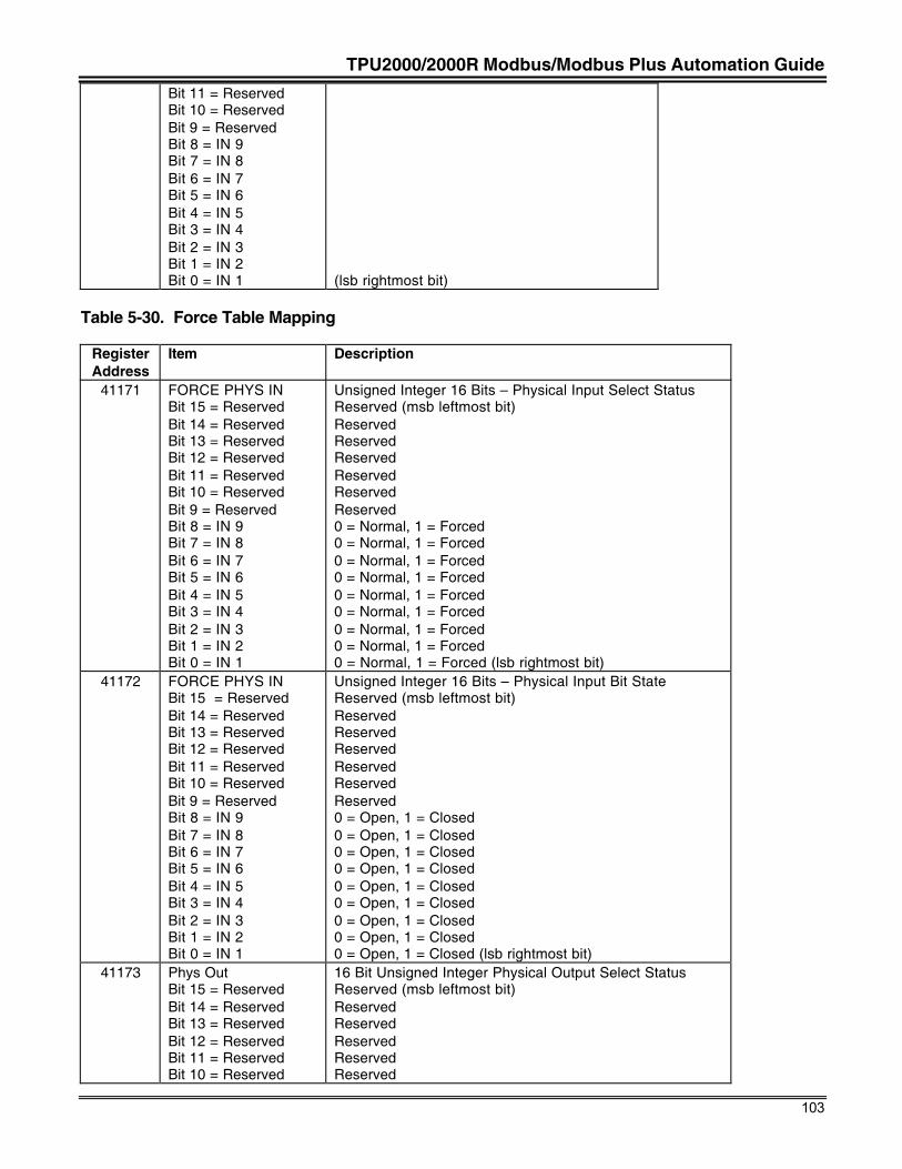
TPU2000/2000R Modbus/Modbus Plus Automation Guide
103
Bit 11 = ReservedBit 10 = ReservedBit 9 = ReservedBit 8 = IN 9Bit 7 = IN 8Bit 6 = IN 7Bit 5 = IN 6Bit 4 = IN 5Bit 3 = IN 4Bit 2 = IN 3Bit 1 = IN 2Bit 0 = IN 1 (lsb rightmost bit)
Table 5-30. Force Table Mapping
RegisterAddress
Item Description
41171 FORCE PHYS INBit 15 = ReservedBit 14 = ReservedBit 13 = ReservedBit 12 = ReservedBit 11 = ReservedBit 10 = ReservedBit 9 = ReservedBit 8 = IN 9Bit 7 = IN 8Bit 6 = IN 7Bit 5 = IN 6Bit 4 = IN 5Bit 3 = IN 4Bit 2 = IN 3Bit 1 = IN 2Bit 0 = IN 1
Unsigned Integer 16 Bits – Physical Input Select StatusReserved (msb leftmost bit)ReservedReservedReservedReservedReservedReserved0 = Normal, 1 = Forced0 = Normal, 1 = Forced0 = Normal, 1 = Forced0 = Normal, 1 = Forced0 = Normal, 1 = Forced0 = Normal, 1 = Forced0 = Normal, 1 = Forced0 = Normal, 1 = Forced0 = Normal, 1 = Forced (lsb rightmost bit)
41172 FORCE PHYS INBit 15 = ReservedBit 14 = ReservedBit 13 = ReservedBit 12 = ReservedBit 11 = ReservedBit 10 = ReservedBit 9 = ReservedBit 8 = IN 9Bit 7 = IN 8Bit 6 = IN 7Bit 5 = IN 6Bit 4 = IN 5Bit 3 = IN 4Bit 2 = IN 3Bit 1 = IN 2Bit 0 = IN 1
Unsigned Integer 16 Bits – Physical Input Bit StateReserved (msb leftmost bit)ReservedReservedReservedReservedReservedReserved0 = Open, 1 = Closed0 = Open, 1 = Closed0 = Open, 1 = Closed0 = Open, 1 = Closed0 = Open, 1 = Closed0 = Open, 1 = Closed0 = Open, 1 = Closed0 = Open, 1 = Closed0 = Open, 1 = Closed (lsb rightmost bit)
41173 Phys OutBit 15 = ReservedBit 14 = ReservedBit 13 = ReservedBit 12 = ReservedBit 11 = ReservedBit 10 = Reserved
16 Bit Unsigned Integer Physical Output Select StatusReserved (msb leftmost bit)ReservedReservedReservedReservedReserved
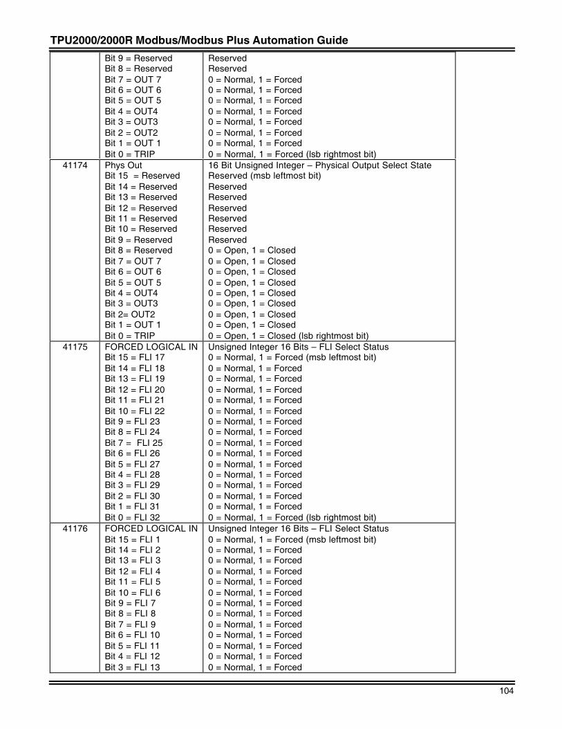
TPU2000/2000R Modbus/Modbus Plus Automation Guide
104
Bit 9 = ReservedBit 8 = ReservedBit 7 = OUT 7Bit 6 = OUT 6Bit 5 = OUT 5Bit 4 = OUT4Bit 3 = OUT3Bit 2 = OUT2Bit 1 = OUT 1Bit 0 = TRIP
ReservedReserved0 = Normal, 1 = Forced0 = Normal, 1 = Forced0 = Normal, 1 = Forced0 = Normal, 1 = Forced0 = Normal, 1 = Forced0 = Normal, 1 = Forced0 = Normal, 1 = Forced0 = Normal, 1 = Forced (lsb rightmost bit)
41174 Phys OutBit 15 = ReservedBit 14 = ReservedBit 13 = ReservedBit 12 = ReservedBit 11 = ReservedBit 10 = ReservedBit 9 = ReservedBit 8 = ReservedBit 7 = OUT 7Bit 6 = OUT 6Bit 5 = OUT 5Bit 4 = OUT4Bit 3 = OUT3Bit 2= OUT2Bit 1 = OUT 1Bit 0 = TRIP
16 Bit Unsigned Integer – Physical Output Select StateReserved (msb leftmost bit)ReservedReservedReservedReservedReservedReserved0 = Open, 1 = Closed0 = Open, 1 = Closed0 = Open, 1 = Closed0 = Open, 1 = Closed0 = Open, 1 = Closed0 = Open, 1 = Closed0 = Open, 1 = Closed0 = Open, 1 = Closed0 = Open, 1 = Closed (lsb rightmost bit)
41175 FORCED LOGICAL INBit 15 = FLI 17Bit 14 = FLI 18Bit 13 = FLI 19Bit 12 = FLI 20Bit 11 = FLI 21Bit 10 = FLI 22Bit 9 = FLI 23Bit 8 = FLI 24Bit 7 = FLI 25Bit 6 = FLI 26Bit 5 = FLI 27Bit 4 = FLI 28Bit 3 = FLI 29Bit 2 = FLI 30Bit 1 = FLI 31Bit 0 = FLI 32
Unsigned Integer 16 Bits – FLI Select Status0 = Normal, 1 = Forced (msb leftmost bit)0 = Normal, 1 = Forced0 = Normal, 1 = Forced0 = Normal, 1 = Forced0 = Normal, 1 = Forced0 = Normal, 1 = Forced0 = Normal, 1 = Forced0 = Normal, 1 = Forced0 = Normal, 1 = Forced0 = Normal, 1 = Forced0 = Normal, 1 = Forced0 = Normal, 1 = Forced0 = Normal, 1 = Forced0 = Normal, 1 = Forced0 = Normal, 1 = Forced0 = Normal, 1 = Forced (lsb rightmost bit)
41176 FORCED LOGICAL INBit 15 = FLI 1Bit 14 = FLI 2Bit 13 = FLI 3Bit 12 = FLI 4Bit 11 = FLI 5Bit 10 = FLI 6Bit 9 = FLI 7Bit 8 = FLI 8Bit 7 = FLI 9Bit 6 = FLI 10Bit 5 = FLI 11Bit 4 = FLI 12Bit 3 = FLI 13
Unsigned Integer 16 Bits – FLI Select Status0 = Normal, 1 = Forced (msb leftmost bit)0 = Normal, 1 = Forced0 = Normal, 1 = Forced0 = Normal, 1 = Forced0 = Normal, 1 = Forced0 = Normal, 1 = Forced0 = Normal, 1 = Forced0 = Normal, 1 = Forced0 = Normal, 1 = Forced0 = Normal, 1 = Forced0 = Normal, 1 = Forced0 = Normal, 1 = Forced0 = Normal, 1 = Forced
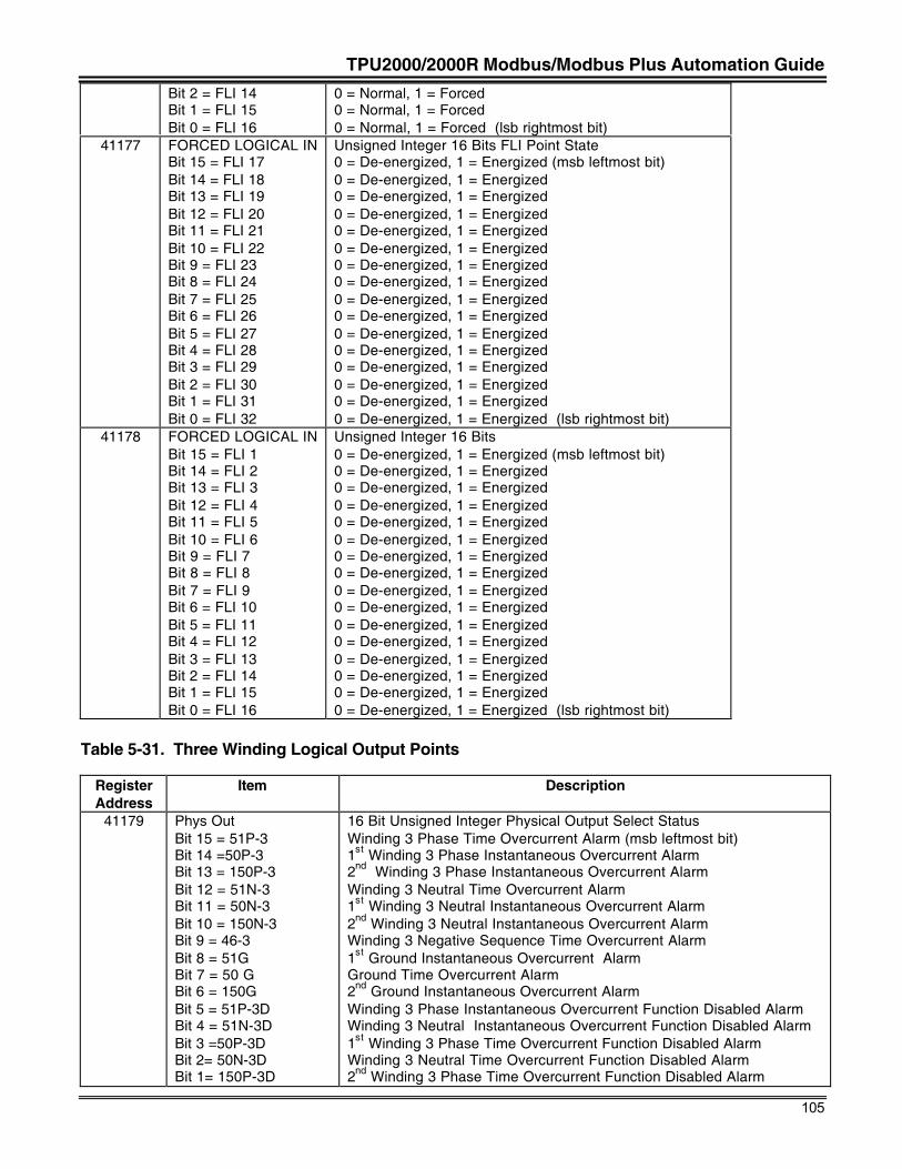
TPU2000/2000R Modbus/Modbus Plus Automation Guide
105
Bit 2 = FLI 14Bit 1 = FLI 15Bit 0 = FLI 16
0 = Normal, 1 = Forced0 = Normal, 1 = Forced0 = Normal, 1 = Forced (lsb rightmost bit)
41177 FORCED LOGICAL INBit 15 = FLI 17Bit 14 = FLI 18Bit 13 = FLI 19Bit 12 = FLI 20Bit 11 = FLI 21Bit 10 = FLI 22Bit 9 = FLI 23Bit 8 = FLI 24Bit 7 = FLI 25Bit 6 = FLI 26Bit 5 = FLI 27Bit 4 = FLI 28Bit 3 = FLI 29Bit 2 = FLI 30Bit 1 = FLI 31Bit 0 = FLI 32
Unsigned Integer 16 Bits FLI Point State0 = De-energized, 1 = Energized (msb leftmost bit)0 = De-energized, 1 = Energized0 = De-energized, 1 = Energized0 = De-energized, 1 = Energized0 = De-energized, 1 = Energized0 = De-energized, 1 = Energized0 = De-energized, 1 = Energized0 = De-energized, 1 = Energized0 = De-energized, 1 = Energized0 = De-energized, 1 = Energized0 = De-energized, 1 = Energized0 = De-energized, 1 = Energized0 = De-energized, 1 = Energized0 = De-energized, 1 = Energized0 = De-energized, 1 = Energized0 = De-energized, 1 = Energized (lsb rightmost bit)
41178 FORCED LOGICAL INBit 15 = FLI 1Bit 14 = FLI 2Bit 13 = FLI 3Bit 12 = FLI 4Bit 11 = FLI 5Bit 10 = FLI 6Bit 9 = FLI 7Bit 8 = FLI 8Bit 7 = FLI 9Bit 6 = FLI 10Bit 5 = FLI 11Bit 4 = FLI 12Bit 3 = FLI 13Bit 2 = FLI 14Bit 1 = FLI 15Bit 0 = FLI 16
Unsigned Integer 16 Bits0 = De-energized, 1 = Energized (msb leftmost bit)0 = De-energized, 1 = Energized0 = De-energized, 1 = Energized0 = De-energized, 1 = Energized0 = De-energized, 1 = Energized0 = De-energized, 1 = Energized0 = De-energized, 1 = Energized0 = De-energized, 1 = Energized0 = De-energized, 1 = Energized0 = De-energized, 1 = Energized0 = De-energized, 1 = Energized0 = De-energized, 1 = Energized0 = De-energized, 1 = Energized0 = De-energized, 1 = Energized0 = De-energized, 1 = Energized0 = De-energized, 1 = Energized (lsb rightmost bit)
Table 5-31. Three Winding Logical Output Points
RegisterAddress
Item Description
41179 Phys OutBit 15 = 51P-3Bit 14 =50P-3Bit 13 = 150P-3Bit 12 = 51N-3Bit 11 = 50N-3Bit 10 = 150N-3Bit 9 = 46-3Bit 8 = 51GBit 7 = 50 GBit 6 = 150GBit 5 = 51P-3DBit 4 = 51N-3DBit 3 =50P-3DBit 2= 50N-3DBit 1= 150P-3D
16 Bit Unsigned Integer Physical Output Select StatusWinding 3 Phase Time Overcurrent Alarm (msb leftmost bit)1st Winding 3 Phase Instantaneous Overcurrent Alarm2nd Winding 3 Phase Instantaneous Overcurrent AlarmWinding 3 Neutral Time Overcurrent Alarm1st Winding 3 Neutral Instantaneous Overcurrent Alarm2nd Winding 3 Neutral Instantaneous Overcurrent AlarmWinding 3 Negative Sequence Time Overcurrent Alarm1st Ground Instantaneous Overcurrent AlarmGround Time Overcurrent Alarm2nd Ground Instantaneous Overcurrent AlarmWinding 3 Phase Instantaneous Overcurrent Function Disabled AlarmWinding 3 Neutral Instantaneous Overcurrent Function Disabled Alarm1st Winding 3 Phase Time Overcurrent Function Disabled AlarmWinding 3 Neutral Time Overcurrent Function Disabled Alarm2nd Winding 3 Phase Time Overcurrent Function Disabled Alarm
TPU2000/2000R Modbus/Modbus Plus Automation Guide
106
Bit 0 = 150N-3D 2nd Winding 3 Neutral Time Overcurrent Function Disabled Alarm (lsbrightmost bit)
41180 Phys OutBit 15 = 46-3
Bit 14 =51GDBit 13 = 50GDBit 12 = 150GDBit 11 = 51P-3(L)Bit 10 = 50P-3 (L)Bit 9 = 150P-3 (L)Bit 8 = 51N-3 (L)Bit 7 = 50N-3 (L)Bit 6 = 150N-3 (L)Bit 5 = 46-3 (L)Bit 4 = 51G (L)Bit 3 = 50G (L)Bit 2 = 150G (L)Bit 1 = TFKA-3 (Note 1)Bit 0 = HLDA-3
16 Bit Unsigned IntegerWinding 3 Negative Sequence Time Overcurrent Alarm (msb leftmostbit)1st Ground Instantaneous Overcurrent Function Disabled Alarm1st Winding 3 Ground Instantaneous Overcurrent Function Disabled2nd Winding 3 Ground Instantaneous Overcurrent Function DisabledWinding 3 Phase Time Overcurrent Alarm Latched1st Winding 3 Phase Instantaneous Overcurrent Alarm Latched2nd Winding 3 Phase Instantaneous Overcurrent Alarm LatchedWinding 3 Neutral Time Overcurrent Alarm Latched1st Winding 3 Neutral Instantaneous Overcurrent Alarm Latched2nd Winding 3 Neutral Instantaneous Overcurrent Alarm LatchedWinding 3 Negative Sequence Time Overcurrent Alarm Latched1st Ground Instantaneous Overcurrent Alarm LatchedGround Time Overcurrent Alarm Latched2nd Ground Instantaneous Overcurrent Alarm LatchedThrough Fault Counter AlarmWinding 3 High Level Detector Alarm (lsb rightmost bit)
41181 Phys OutBit 15 = LLDA –3Bit 14 = OCA-3Bit 13 = Pwatt3Bit 12 = OCA GndBit 11 = ReservedBit 10 = ReservedBit 9 = ReservedBit 8 = ReservedBit 7 = ReservedBit 6 = ReservedBit 5 = ReservedBit 4= ReservedBit 3 = ReservedBit 2 = ReservedBit 1 = ReservedBit 0 = Reserved
16 Bit Unsigned Integer Physical Output Select StatusWinding 3 Low Level Detector Alarm (msb leftmost bit)Winding 3 Overcurrent AlarmWinding 3 Positive 3 Phase Watt AlarmGround Overcurrent AlarmReservedReservedReservedReservedReservedReservedReservedReservedReservedReservedReservedReserved (lsb rightmost bit)
41182 Phys OutReserved
16 Bit Unsigned Integer Physical Output Select StatusReserved
4X Register Write Capabilities
All of the Modbus status retrieval have involved 03 register read commands only. Modbus allows for two types ofcommands involving control writes to obtain read data. One Modbus command allows register writes. AnotherModbus command allows for register writes and reads with one command. The type of functionality performedwith relay writes is as such:
• Access of Differential Fault Records (2 Winding and 3 Winding Values)• Access of Through Fault Records (2 Winding and 3 Winding Values)• Access of Harmonic Restraint Fault Records (2 Winding and 3 Winding Values)• Access of Operation Records• Trip Initiation• Enable/Disable of Protective Functions• Clearing of Event Counters• Enable/Disable of Supervisory Functions• Reset of Targets• Clear of Seal In’s
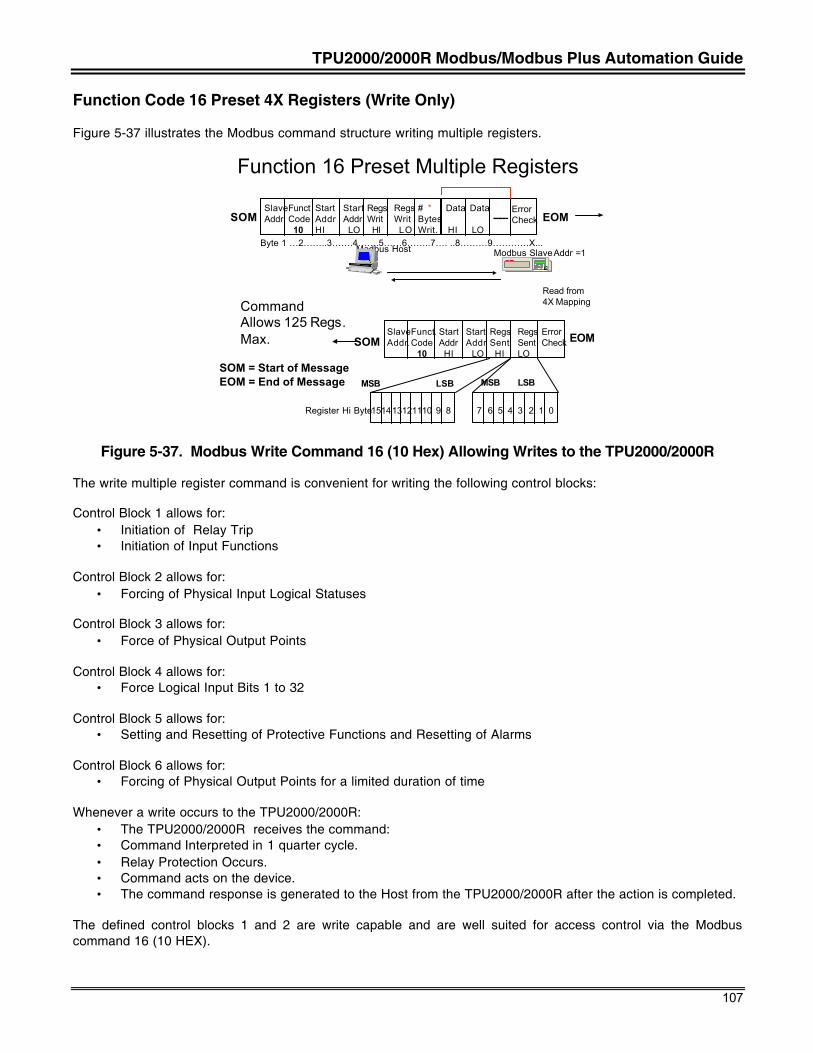
TPU2000/2000R Modbus/Modbus Plus Automation Guide
107
Function Code 16 Preset 4X Registers (Write Only)
Figure 5-37 illustrates the Modbus command structure writing multiple registers.
Function 16 Preset Multiple Registers
Modbus Host Modbus Slave Addr =1
Read from 4X Mapping
SlaveAddr.
Funct.Code 10
StartAddrHI
Start Addr LO
RegsWrit HI
RegsWrit LO
# *BytesWrit.
EOMSOM
SlaveAddr.
Funct.Code 10
StartAddr HI
StartAddr LO
RegsSent HI
RegsSentLO
ErrorCheck EOMSOM
Byte 1 …2……..3…….4…….5……6……..7…. ..8………9…………X...
MSB LSB
151413121110 9 8 7 6 5 4 3 2 1 0
MSB LSB
Register Hi Byte
Data
HI
Data
LO
ErrorCheck
CommandAllows 125 Regs.Max.
EC
SOM = Start of MessageEOM = End of Message
Figure 5-37. Modbus Write Command 16 (10 Hex) Allowing Writes to the TPU2000/2000R
The write multiple register command is convenient for writing the following control blocks:
Control Block 1 allows for:• Initiation of Relay Trip• Initiation of Input Functions
Control Block 2 allows for:• Forcing of Physical Input Logical Statuses
Control Block 3 allows for:• Force of Physical Output Points
Control Block 4 allows for:• Force Logical Input Bits 1 to 32
Control Block 5 allows for:• Setting and Resetting of Protective Functions and Resetting of Alarms
Control Block 6 allows for:• Forcing of Physical Output Points for a limited duration of time
Whenever a write occurs to the TPU2000/2000R:• The TPU2000/2000R receives the command:• Command Interpreted in 1 quarter cycle.• Relay Protection Occurs.• Command acts on the device.• The command response is generated to the Host from the TPU2000/2000R after the action is completed.
The defined control blocks 1 and 2 are write capable and are well suited for access control via the Modbuscommand 16 (10 HEX).
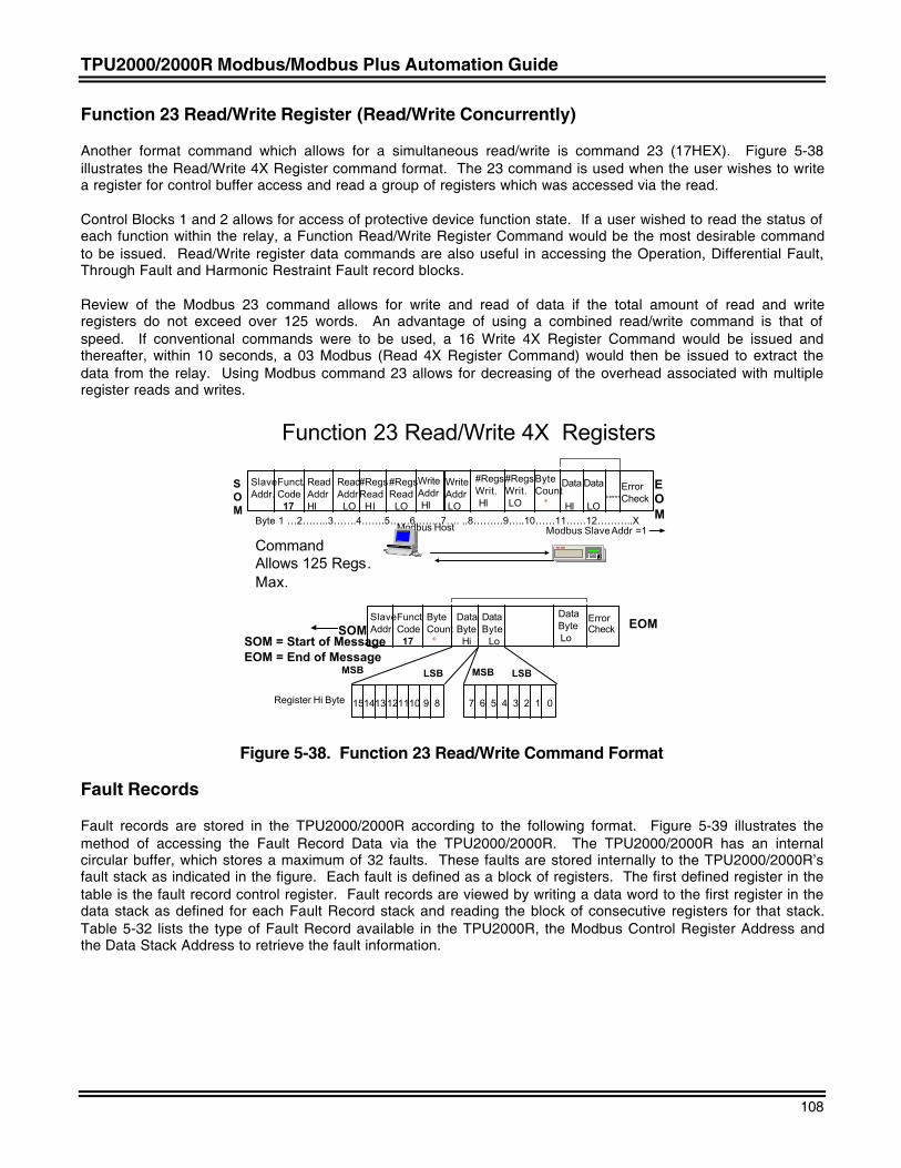
TPU2000/2000R Modbus/Modbus Plus Automation Guide
108
Function 23 Read/Write Register (Read/Write Concurrently)
Another format command which allows for a simultaneous read/write is command 23 (17HEX). Figure 5-38illustrates the Read/Write 4X Register command format. The 23 command is used when the user wishes to writea register for control buffer access and read a group of registers which was accessed via the read.
Control Blocks 1 and 2 allows for access of protective device function state. If a user wished to read the status ofeach function within the relay, a Function Read/Write Register Command would be the most desirable commandto be issued. Read/Write register data commands are also useful in accessing the Operation, Differential Fault,Through Fault and Harmonic Restraint Fault record blocks.
Review of the Modbus 23 command allows for write and read of data if the total amount of read and writeregisters do not exceed over 125 words. An advantage of using a combined read/write command is that ofspeed. If conventional commands were to be used, a 16 Write 4X Register Command would be issued andthereafter, within 10 seconds, a 03 Modbus (Read 4X Register Command) would then be issued to extract thedata from the relay. Using Modbus command 23 allows for decreasing of the overhead associated with multipleregister reads and writes.
Function 23 Read/Write 4X Registers
Modbus Host
EC
Modbus Slave Addr =1
SlaveAddr.
Funct.Code 17
ReadAddrHI
Read Addr LO
#RegsRead HI
#RegsRead LO
Byte 1 …2……..3…….4…….5……6……..7…. ..8………9…..10……11……12………..X
Data
HI
Data
LO
ErrorCheck
CommandAllows 125 Regs.Max.
WriteAddr HI
WriteAddr LO
#RegsWrit. HI
#RegsWrit. LO
ByteCount *
SlaveAddr.
Funct.Code 17
ByteCount *
DataByte Hi
DataByte Lo
DataByte Lo
ErrorCheck EOMSOM
MSB LSB
151413121110 9 8 7 6 5 4 3 2 1 0
MSB LSB
Register Hi Byte
SOM
EOM
SOM = Start of MessageEOM = End of Message
Figure 5-38. Function 23 Read/Write Command Format
Fault Records
Fault records are stored in the TPU2000/2000R according to the following format. Figure 5-39 illustrates themethod of accessing the Fault Record Data via the TPU2000/2000R. The TPU2000/2000R has an internalcircular buffer, which stores a maximum of 32 faults. These faults are stored internally to the TPU2000/2000R’sfault stack as indicated in the figure. Each fault is defined as a block of registers. The first defined register in thetable is the fault record control register. Fault records are viewed by writing a data word to the first register in thedata stack as defined for each Fault Record stack and reading the block of consecutive registers for that stack.Table 5-32 lists the type of Fault Record available in the TPU2000R, the Modbus Control Register Address andthe Data Stack Address to retrieve the fault information.
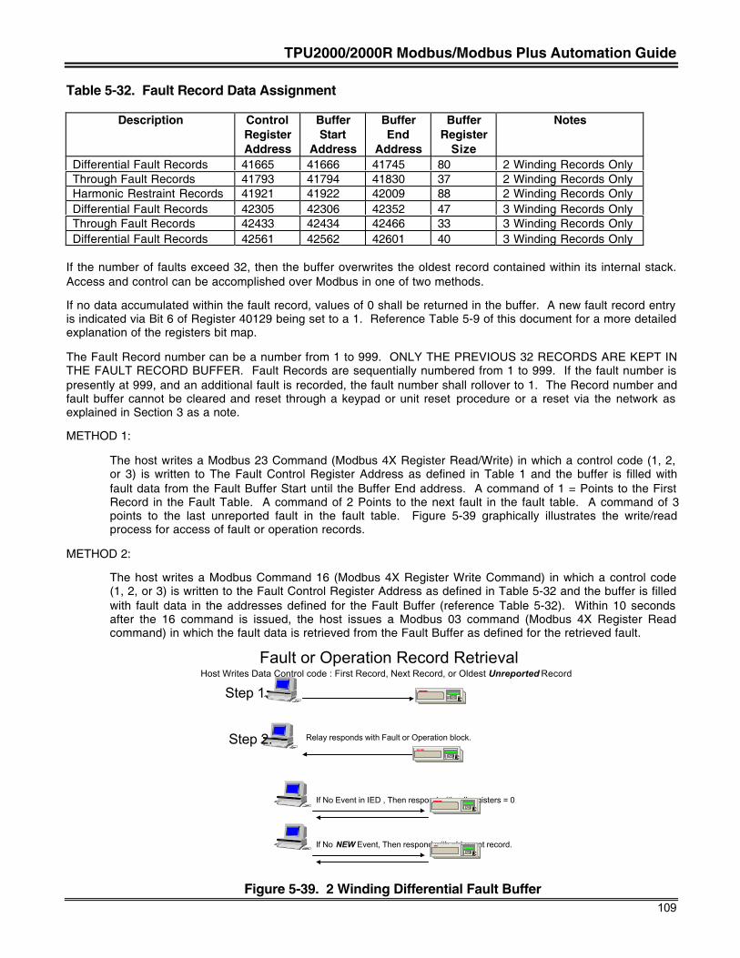
TPU2000/2000R Modbus/Modbus Plus Automation Guide
109
Table 5-32. Fault Record Data Assignment
Description ControlRegisterAddress
BufferStart
Address
BufferEnd
Address
BufferRegister
Size
Notes
Differential Fault Records 41665 41666 41745 80 2 Winding Records OnlyThrough Fault Records 41793 41794 41830 37 2 Winding Records OnlyHarmonic Restraint Records 41921 41922 42009 88 2 Winding Records OnlyDifferential Fault Records 42305 42306 42352 47 3 Winding Records OnlyThrough Fault Records 42433 42434 42466 33 3 Winding Records OnlyDifferential Fault Records 42561 42562 42601 40 3 Winding Records Only
If the number of faults exceed 32, then the buffer overwrites the oldest record contained within its internal stack.Access and control can be accomplished over Modbus in one of two methods.
If no data accumulated within the fault record, values of 0 shall be returned in the buffer. A new fault record entryis indicated via Bit 6 of Register 40129 being set to a 1. Reference Table 5-9 of this document for a more detailedexplanation of the registers bit map.
The Fault Record number can be a number from 1 to 999. ONLY THE PREVIOUS 32 RECORDS ARE KEPT INTHE FAULT RECORD BUFFER. Fault Records are sequentially numbered from 1 to 999. If the fault number ispresently at 999, and an additional fault is recorded, the fault number shall rollover to 1. The Record number andfault buffer cannot be cleared and reset through a keypad or unit reset procedure or a reset via the network asexplained in Section 3 as a note.
METHOD 1:
The host writes a Modbus 23 Command (Modbus 4X Register Read/Write) in which a control code (1, 2,or 3) is written to The Fault Control Register Address as defined in Table 1 and the buffer is filled withfault data from the Fault Buffer Start until the Buffer End address. A command of 1 = Points to the FirstRecord in the Fault Table. A command of 2 Points to the next fault in the fault table. A command of 3points to the last unreported fault in the fault table. Figure 5-39 graphically illustrates the write/readprocess for access of fault or operation records.
METHOD 2:
The host writes a Modbus Command 16 (Modbus 4X Register Write Command) in which a control code(1, 2, or 3) is written to the Fault Control Register Address as defined in Table 5-32 and the buffer is filledwith fault data in the addresses defined for the Fault Buffer (reference Table 5-32). Within 10 secondsafter the 16 command is issued, the host issues a Modbus 03 command (Modbus 4X Register Readcommand) in which the fault data is retrieved from the Fault Buffer as defined for the retrieved fault.
Fault or Operation Record Retrieval
Step 1.
Step 2.
Host Writes Data Control code : First Record, Next Record, or Oldest Unreported Record
Relay responds with Fault or Operation block.
If No Event in IED , Then respond with all registers = 0
If No NEW Event, Then respond with old event record.
EC
EC
EC
EC
Figure 5-39. 2 Winding Differential Fault Buffer
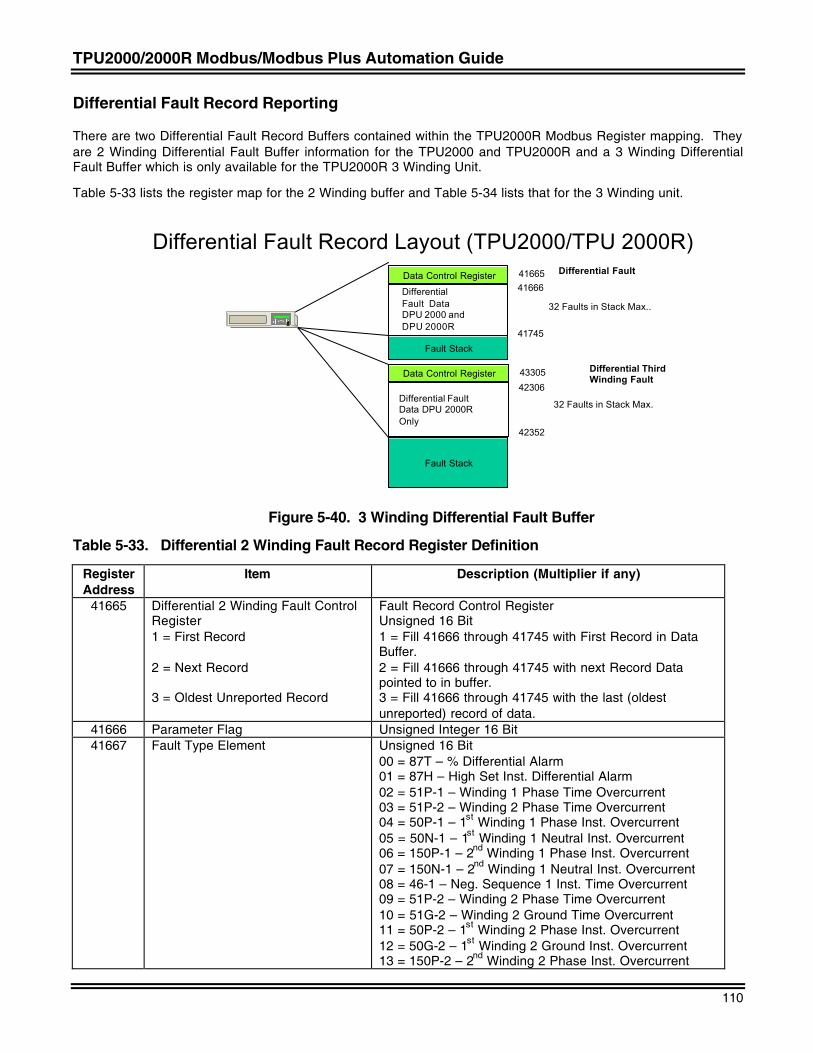
TPU2000/2000R Modbus/Modbus Plus Automation Guide
110
Differential Fault Record Reporting
There are two Differential Fault Record Buffers contained within the TPU2000R Modbus Register mapping. Theyare 2 Winding Differential Fault Buffer information for the TPU2000 and TPU2000R and a 3 Winding DifferentialFault Buffer which is only available for the TPU2000R 3 Winding Unit.
Table 5-33 lists the register map for the 2 Winding buffer and Table 5-34 lists that for the 3 Winding unit.
Differential Fault Record Layout (TPU2000/TPU 2000R)Data Control Register
DifferentialFault DataDPU 2000 andDPU 2000R
4166541666
41745
Differential Fault
Data Control Register
Differential FaultData DPU 2000ROnly
43305
42306
42352
32 Faults in Stack Max..
32 Faults in Stack Max.
Fault Stack
Fault Stack
Differential Third Winding Fault
EC
Figure 5-40. 3 Winding Differential Fault Buffer
Table 5-33. Differential 2 Winding Fault Record Register Definition
RegisterAddress
Item Description (Multiplier if any)
41665 Differential 2 Winding Fault ControlRegister1 = First Record
2 = Next Record
3 = Oldest Unreported Record
Fault Record Control RegisterUnsigned 16 Bit1 = Fill 41666 through 41745 with First Record in DataBuffer.2 = Fill 41666 through 41745 with next Record Datapointed to in buffer.3 = Fill 41666 through 41745 with the last (oldestunreported) record of data.
41666 Parameter Flag Unsigned Integer 16 Bit41667 Fault Type Element Unsigned 16 Bit
00 = 87T – % Differential Alarm01 = 87H – High Set Inst. Differential Alarm02 = 51P-1 – Winding 1 Phase Time Overcurrent03 = 51P-2 – Winding 2 Phase Time Overcurrent04 = 50P-1 – 1st Winding 1 Phase Inst. Overcurrent05 = 50N-1 – 1st Winding 1 Neutral Inst. Overcurrent06 = 150P-1 – 2nd Winding 1 Phase Inst. Overcurrent07 = 150N-1 – 2nd Winding 1 Neutral Inst. Overcurrent08 = 46-1 – Neg. Sequence 1 Inst. Time Overcurrent09 = 51P-2 – Winding 2 Phase Time Overcurrent10 = 51G-2 – Winding 2 Ground Time Overcurrent11 = 50P-2 – 1st Winding 2 Phase Inst. Overcurrent12 = 50G-2 – 1st Winding 2 Ground Inst. Overcurrent13 = 150P-2 – 2nd Winding 2 Phase Inst. Overcurrent
TPU2000/2000R Modbus/Modbus Plus Automation Guide
111
RegisterAddress
Item Description (Multiplier if any)
14 = 150G-2 – 2nd Winding 2 Ground Inst. Overcurrent15 = 46-2 – Neg. Sequence 2 Inst. Time Overcurrent16 = ECI-1 – Event Capture Initiate 117 = ECI-2 – Event Capture Initiate 218 = Through Fault19 = Harmonic Restraint
41668 Setting At Fault Event Unsigned 16 Bit01 = Primary Settings02 = Alternate 1 Settings03 = Alternate 2 Settings
41669 Fault Record Number Unsigned 16 Bit(1 – 999, only last 32 kept)
41670 Year 2 digit 00 -99 Unsigned 16 Bit Year of Fault41671 Month 1 - 12 Unsigned 16 Bit Month of Fault41672 Day 1 - 31 Unsigned 16 Bit Day of Fault41673 Hour 00 - 23 Unsigned 16 Bit Hour of Fault41674 Minute 00 - 59 Unsigned 16 Bit Minute of Fault41675 Second 00 - 59 Unsigned 16 Bit Second of Fault41676 Hundredths of Seconds 0 - 99 Unsigned 16 Bit Hundredth Second of Fault Time41677 Clear Time Unsigned 16 Bit (X 1000) seconds41678 Winding1 Tap Unsigned 16 Bit (X 500)41679 Winding2 Tap Unsigned 16 Bit (X 800)41680 I operate Phase A Unsigned 16 Bit (X 800)41681 I operate Phase B Unsigned 16 Bit (X 800)41682 I operate Phase C Unsigned 16 Bit (X 800)41683 I restraint Phase A-Winding 1 Unsigned 16 Bit (X 800)41684 I restraint Phase B-Winding 1 Unsigned 16 Bit (X 800)41685 I restraint Phase C-Winding 1 Unsigned 16 Bit (X 800)41686 I restraint Phase A-Winding 2 Unsigned 16 Bit (X 800)41687 I restraint Phase B-Winding 2 Unsigned 16 Bit (X 800)41688 I restraint Phase C-Winding 2 Unsigned 16 Bit (X 800)41689 2nd Harmonic Phase A-Winding 1 Unsigned 16 Bit (X 2)41690 5th Harmonic Phase A-Winding 1 Unsigned 16 Bit (X 2)41691 All Harmonic Phase A-Winding 1 Unsigned 16 Bit (X 2)41692 2nd Harmonic Phase B-Winding 1 Unsigned 16 Bit (X 2)41693 5th Harmonic Phase B-Winding 1 Unsigned 16 Bit (X 2)41694 All Harmonic Phase B-Winding 1 Unsigned 16 Bit (X 2)41695 2nd Harmonic Phase C-Winding 1 Unsigned 16 Bit (X 2)41696 5th Harmonic Phase C-Winding 1 Unsigned 16 Bit (X 2)41697 All Harmonic Phase C-Winding 1 Unsigned 16 Bit (X 2)41698 2nd Harmonic Phase A-Winding 2 Unsigned 16 Bit (X 2)41699 5th Harmonic Phase A-Winding 2 Unsigned 16 Bit (X 2)41700 All Harmonic Phase A-Winding 2 Unsigned 16 Bit (X 2)41701 2nd Harmonic Phase B-Winding 2 Unsigned 16 Bit (X 2)41702 5th Harmonic Phase B-Winding 2 Unsigned 16 Bit (X 2)41703 All Harmonic Phase B-Winding 2 Unsigned 16 Bit (X 2)41704 2nd Harmonic Phase C-Winding 2 Unsigned 16 Bit (X 2)41705 5th Harmonic Phase C-Winding 2 Unsigned 16 Bit (X 2)41706 All Harmonic Phase C-Winding 2 Unsigned 16 Bit (X 2)41707 I restraint Phase A-Winding 1 (Ang) Unsigned 16 Bit41708 I restraint Phase B-Winding 1 (Ang) Unsigned 16 Bit41709 I restraint Phase C-Winding 1 (Ang) Unsigned 16 Bit41710 I restraint Phase A-Winding 2 (Ang) Unsigned 16 Bit41711 I restraint Phase B-Winding 2 (Ang) Unsigned 16 Bit
TPU2000/2000R Modbus/Modbus Plus Automation Guide
112
RegisterAddress
Item Description (Multiplier if any)
41712 I restraint Phase C-Winding 2 (Ang) Unsigned 16 Bit41713 I Phase A-Winding 1 Unsigned 16 Bit (X 800)41714 I PhaseB-Winding 1 Unsigned 16 Bit (X 800)41715 I Phase C-Winding 1 Unsigned 16 Bit (X 800)41716 I Neutral-Winding 1 Unsigned 16 Bit (X 800)41717 I Phase A-Winding 2 Unsigned 16 Bit (X 800)41718 I Phase B-Winding 2 Unsigned 16 Bit (X 800)41719 I Phase C-Winding 2 Unsigned 16 Bit (X 800)41720 I Neutral-Winding 2 Unsigned 16 Bit (X 800)41721 Spare Unsigned 16 Bit41722 I Phase A-Winding 1 (Ang) Unsigned 16 Bit41723 I Phase B-Winding 1 (Ang) Unsigned 16 Bit41724 I Phase C-Winding 1 (Ang) Unsigned 16 Bit41725 I Neutral-Winding 1 (Ang) Unsigned 16 Bit41726 I Phase A-Winding 2 (Ang) Unsigned 16 Bit41727 I Phase B-Winding 2 (Ang) Unsigned 16 Bit41728 I Phase C-Winding 2 (Ang) Unsigned 16 Bit41729 I Neutral-Winding 2 (Ang) Unsigned 16 Bit41730 I 0-1 – Zero Sequence Current
Winding 1Unsigned 16 Bit (X 800)
41731 I 1-1 – Positive Sequence CurrentWinding 1
Unsigned 16 Bit (X 800)
41732 I 2-1 – Negative Sequence CurrentWinding 1
Unsigned 16 Bit (X 800)
41733 I 0-2 – Zero Sequence CurrentWinding 2
Unsigned 16 Bit (X 800)
41734 I 1-2 – Positive Sequence CurrentWinding 2
Unsigned 16 Bit (X 800)
41735 I 2-2 – Negative Sequence CurrentWinding 2
Unsigned 16 Bit (X 800)
41736 I 0-1 (Ang) – Zero Sequence AngleWinding 1
Unsigned 16 Bit
41737 I 1-1 (Ang) – Positive SequenceAngle Winding 1
Unsigned 16 Bit
41738 I 2-1 (Ang) – Negative SequenceAngle Winding 1
Unsigned 16 Bit
41739 I 0-2 (Ang) – Zero Sequence AngleWinding 2
Unsigned 16 Bit
41740 I 1-2 (Ang) – Positive SequenceAngle Winding 2
Unsigned 16 Bit
41741 I 2-2 (Ang) – Negative SequenceAngle Winding 2
Unsigned 16 Bit
41742 Scale - Phase Wdg 1 Unsigned 16 Bit41743 Scale - Phase Wdg 2 Unsigned 16 Bit41744 Scale - Neutral Wdg 1 Unsigned 16 Bit41745 Scale - Neutral Wdg 2 Unsigned 16 Bit
The 3 Winding Differential Fault Register Definition Table follows.
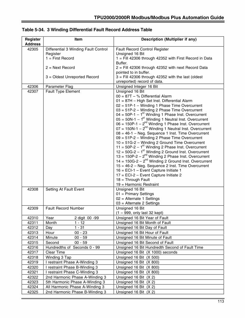
TPU2000/2000R Modbus/Modbus Plus Automation Guide
113
Table 5-34. 3 Winding Differential Fault Record Address Table
RegisterAddress
Item Description (Multiplier if any)
42305 Differential 3 Winding Fault ControlRegister1 = First Record
2 = Next Record
3 = Oldest Unreported Record
Fault Record Control RegisterUnsigned 16 Bit1 = Fill 42306 through 42352 with First Record in DataBuffer.2 = Fill 42306 through 42352 with next Record Datapointed to in buffer.3 = Fill 42306 through 42352 with the last (oldestunreported) record of data.
42306 Parameter Flag Unsigned Integer 16 Bit42307 Fault Type Element Unsigned 16 Bit
00 = 87T – % Differential Alarm01 = 87H – High Set Inst. Differential Alarm02 = 51P-1 – Winding 1 Phase Time Overcurrent03 = 51P-2 – Winding 2 Phase Time Overcurrent04 = 50P-1 – 1st Winding 1 Phase Inst. Overcurrent05 = 50N-1 – 1st Winding 1 Neutral Inst. Overcurrent06 = 150P-1 – 2nd Winding 1 Phase Inst. Overcurrent07 = 150N-1 – 2nd Winding 1 Neutral Inst. Overcurrent08 = 46-1 – Neg. Sequence 1 Inst. Time Overcurrent09 = 51P-2 – Winding 2 Phase Time Overcurrent10 = 51G-2 – Winding 2 Ground Time Overcurrent11 = 50P-2 – 1st Winding 2 Phase Inst. Overcurrent12 = 50G-2 – 1st Winding 2 Ground Inst. Overcurrent13 = 150P-2 – 2nd Winding 2 Phase Inst. Overcurrent14 = 150G-2 – 2nd Winding 2 Ground Inst. Overcurrent15 = 46-2 – Neg. Sequence 2 Inst. Time Overcurrent16 = ECI-1 – Event Capture Initiate 117 = ECI-2 – Event Capture Initiate 218 = Through Fault19 = Harmonic Restraint
42308 Setting At Fault Event Unsigned 16 Bit01 = Primary Settings02 = Alternate 1 Settings03 = Alternate 2 Settings
42309 Fault Record Number Unsigned 16 Bit(1 – 999, only last 32 kept)
42310 Year 2 digit 00 -99 Unsigned 16 Bit Year of Fault42311 Month 1 - 12 Unsigned 16 Bit Month of Fault42312 Day 1 - 31 Unsigned 16 Bit Day of Fault42313 Hour 00 - 23 Unsigned 16 Bit Hour of Fault42314 Minute 00 - 59 Unsigned 16 Bit Minute of Fault42315 Second 00 - 59 Unsigned 16 Bit Second of Fault42316 Hundredths of Seconds 0 - 99 Unsigned 16 Bit Hundredth Second of Fault Time42317 Clear Time Unsigned 16 Bit (X 1000) seconds42318 Winding 3 Tap Unsigned 16 Bit (X 500)42319 I restraint Phase A-Winding 3 Unsigned 16 Bit (X 800)42320 I restraint Phase B-Winding 3 Unsigned 16 Bit (X 800)42321 I restraint Phase C-Winding 3 Unsigned 16 Bit (X 800)42322 2nd Harmonic Phase A-Winding 3 Unsigned 16 Bit (X 2)42323 5th Harmonic Phase A-Winding 3 Unsigned 16 Bit (X 2)42324 All Harmonic Phase A-Winding 3 Unsigned 16 Bit (X 2)42325 2nd Harmonic Phase B-Winding 3 Unsigned 16 Bit (X 2)
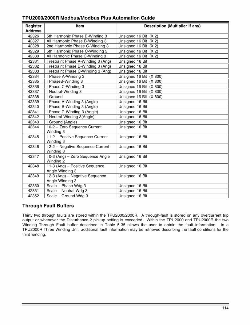
TPU2000/2000R Modbus/Modbus Plus Automation Guide
114
RegisterAddress
Item Description (Multiplier if any)
42326 5th Harmonic Phase B-Winding 3 Unsigned 16 Bit (X 2)42327 All Harmonic Phase B-Winding 3 Unsigned 16 Bit (X 2)42328 2nd Harmonic Phase C-Winding 3 Unsigned 16 Bit (X 2)42329 5th Harmonic Phase C-Winding 3 Unsigned 16 Bit (X 2)42330 All Harmonic Phase C-Winding 3 Unsigned 16 Bit (X 2)42331 I restraint Phase A-Winding 3 (Ang) Unsigned 16 Bit42332 I restraint Phase B-Winding 3 (Ang) Unsigned 16 Bit42333 I restraint Phase C-Winding 3 (Ang) Unsigned 16 Bit42334 I Phase A-Winding 3 Unsigned 16 Bit (X 800)42335 I PhaseB-Winding 3 Unsigned 16 Bit (X 800)42336 I Phase C-Winding 3 Unsigned 16 Bit (X 800)42337 I Neutral-Winding 3 Unsigned 16 Bit (X 800)42338 I Ground Unsigned 16 Bit (X 800)42339 I Phase A-Winding 3 (Angle) Unsigned 16 Bit42340 I Phase B-Winding 3 (Angle) Unsigned 16 Bit42341 I Phase C-Winding 3 (Angle) Unsigned 16 Bit42342 I Neutral-Winding 3(Angle) Unsigned 16 Bit42343 I Ground (Angle) Unsigned 16 Bit42344 I 0-2 – Zero Sequence Current
Winding 3Unsigned 16 Bit
42345 I 1-2 – Positive Sequence CurrentWinding 3
Unsigned 16 Bit
42346 I 2-2 – Negative Sequence CurrentWinding 3
Unsigned 16 Bit
42347 I 0-3 (Ang) – Zero Sequence AngleWinding 2
Unsigned 16 Bit
42348 I 1-3 (Ang) – Positive SequenceAngle Winding 3
Unsigned 16 Bit
42349 I 2-3 (Ang) – Negative SequenceAngle Winding 3
Unsigned 16 Bit
42350 Scale – Phase Wdg 3 Unsigned 16 Bit42351 Scale – Neutral Wdg 3 Unsigned 16 Bit42352 Scale – Ground Wdg 3 Unsigned 16 Bit
Through Fault Buffers
Thirty two through faults are stored within the TPU2000/2000R. A through-fault is stored on any overcurrent tripoutput or whenever the Disturbance-2 pickup setting is exceeded. Within the TPU2000 and TPU2000R the twoWinding Through Fault buffer described in Table 5-35 allows the user to obtain the fault information. In aTPU2000R Three Winding Unit, additional fault information may be retrieved describing the fault conditions for thethird winding.
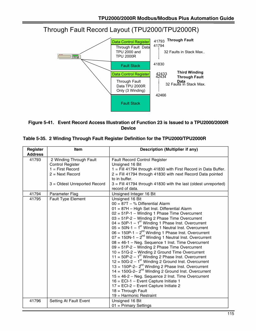
TPU2000/2000R Modbus/Modbus Plus Automation Guide
115
Through Fault Record Layout (TPU2000/TPU2000R)
Data Control RegisterThrough Fault DataTPU 2000 andTPU 2000R
4179341794
41830
Through Fault
Data Control Register
Through FaultData TPU 2000ROnly (3 Winding)
4243342434
42466
32 Faults in Stack Max..
32 Faults in Stack Max.
Fault Stack
Fault Stack
Third Winding Through FaultData
EC
Figure 5-41. Event Record Access Illustration of Function 23 is Issued to a TPU2000/2000RDevice
Table 5-35. 2 Winding Through Fault Register Definition for the TPU2000/TPU2000R
RegisterAddress
Item Description (Multiplier if any)
41793 2 Winding Through FaultControl Register1 = First Record2 = Next Record
3 = Oldest Unreported Record
Fault Record Control RegisterUnsigned 16 Bit1 = Fill 41794 through 41830 with First Record in Data Buffer.2 = Fill 41794 through 41830 with next Record Data pointedto in buffer.3 = Fill 41794 through 41830 with the last (oldest unreported)record of data.
41794 Parameter Flag Unsigned Integer 16 Bit41795 Fault Type Element Unsigned 16 Bit
00 = 87T – % Differential Alarm01 = 87H – High Set Inst. Differential Alarm02 = 51P-1 – Winding 1 Phase Time Overcurrent03 = 51P-2 – Winding 2 Phase Time Overcurrent04 = 50P-1 – 1st Winding 1 Phase Inst. Overcurrent05 = 50N-1 – 1st Winding 1 Neutral Inst. Overcurrent06 = 150P-1 – 2nd Winding 1 Phase Inst. Overcurrent07 = 150N-1 – 2nd Winding 1 Neutral Inst. Overcurrent08 = 46-1 – Neg. Sequence 1 Inst. Time Overcurrent09 = 51P-2 – Winding 2 Phase Time Overcurrent10 = 51G-2 – Winding 2 Ground Time Overcurrent11 = 50P-2 – 1st Winding 2 Phase Inst. Overcurrent12 = 50G-2 – 1st Winding 2 Ground Inst. Overcurrent13 = 150P-2– 2nd Winding 2 Phase Inst. Overcurrent14 = 150G-2– 2nd Winding 2 Ground Inst. Overcurrent15 = 46-2 – Neg. Sequence 2 Inst. Time Overcurrent16 = ECI-1 – Event Capture Initiate 117 = ECI-2 – Event Capture Initiate 218 = Through Fault19 = Harmonic Restraint
41796 Setting At Fault Event Unsigned 16 Bit01 = Primary Settings
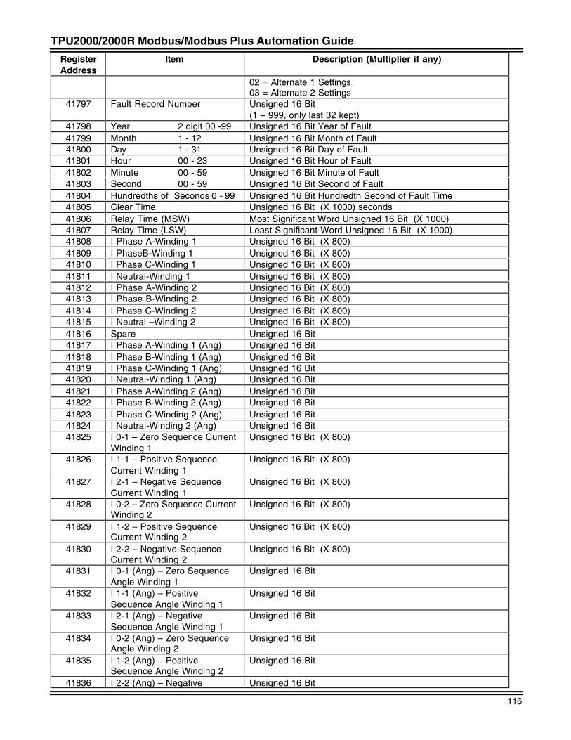
TPU2000/2000R Modbus/Modbus Plus Automation Guide
116
RegisterAddress
Item Description (Multiplier if any)
02 = Alternate 1 Settings03 = Alternate 2 Settings
41797 Fault Record Number Unsigned 16 Bit(1 – 999, only last 32 kept)
41798 Year 2 digit 00 -99 Unsigned 16 Bit Year of Fault41799 Month 1 - 12 Unsigned 16 Bit Month of Fault41800 Day 1 - 31 Unsigned 16 Bit Day of Fault41801 Hour 00 - 23 Unsigned 16 Bit Hour of Fault41802 Minute 00 - 59 Unsigned 16 Bit Minute of Fault41803 Second 00 - 59 Unsigned 16 Bit Second of Fault41804 Hundredths of Seconds 0 - 99 Unsigned 16 Bit Hundredth Second of Fault Time41805 Clear Time Unsigned 16 Bit (X 1000) seconds41806 Relay Time (MSW) Most Significant Word Unsigned 16 Bit (X 1000)41807 Relay Time (LSW) Least Significant Word Unsigned 16 Bit (X 1000)41808 I Phase A-Winding 1 Unsigned 16 Bit (X 800)41809 I PhaseB-Winding 1 Unsigned 16 Bit (X 800)41810 I Phase C-Winding 1 Unsigned 16 Bit (X 800)41811 I Neutral-Winding 1 Unsigned 16 Bit (X 800)41812 I Phase A-Winding 2 Unsigned 16 Bit (X 800)41813 I Phase B-Winding 2 Unsigned 16 Bit (X 800)41814 I Phase C-Winding 2 Unsigned 16 Bit (X 800)41815 I Neutral –Winding 2 Unsigned 16 Bit (X 800)41816 Spare Unsigned 16 Bit41817 I Phase A-Winding 1 (Ang) Unsigned 16 Bit41818 I Phase B-Winding 1 (Ang) Unsigned 16 Bit41819 I Phase C-Winding 1 (Ang) Unsigned 16 Bit41820 I Neutral-Winding 1 (Ang) Unsigned 16 Bit41821 I Phase A-Winding 2 (Ang) Unsigned 16 Bit41822 I Phase B-Winding 2 (Ang) Unsigned 16 Bit41823 I Phase C-Winding 2 (Ang) Unsigned 16 Bit41824 I Neutral-Winding 2 (Ang) Unsigned 16 Bit41825 I 0-1 – Zero Sequence Current
Winding 1Unsigned 16 Bit (X 800)
41826 I 1-1 – Positive SequenceCurrent Winding 1
Unsigned 16 Bit (X 800)
41827 I 2-1 – Negative SequenceCurrent Winding 1
Unsigned 16 Bit (X 800)
41828 I 0-2 – Zero Sequence CurrentWinding 2
Unsigned 16 Bit (X 800)
41829 I 1-2 – Positive SequenceCurrent Winding 2
Unsigned 16 Bit (X 800)
41830 I 2-2 – Negative SequenceCurrent Winding 2
Unsigned 16 Bit (X 800)
41831 I 0-1 (Ang) – Zero SequenceAngle Winding 1
Unsigned 16 Bit
41832 I 1-1 (Ang) – PositiveSequence Angle Winding 1
Unsigned 16 Bit
41833 I 2-1 (Ang) – NegativeSequence Angle Winding 1
Unsigned 16 Bit
41834 I 0-2 (Ang) – Zero SequenceAngle Winding 2
Unsigned 16 Bit
41835 I 1-2 (Ang) – PositiveSequence Angle Winding 2
Unsigned 16 Bit
41836 I 2-2 (Ang) – Negative Unsigned 16 Bit
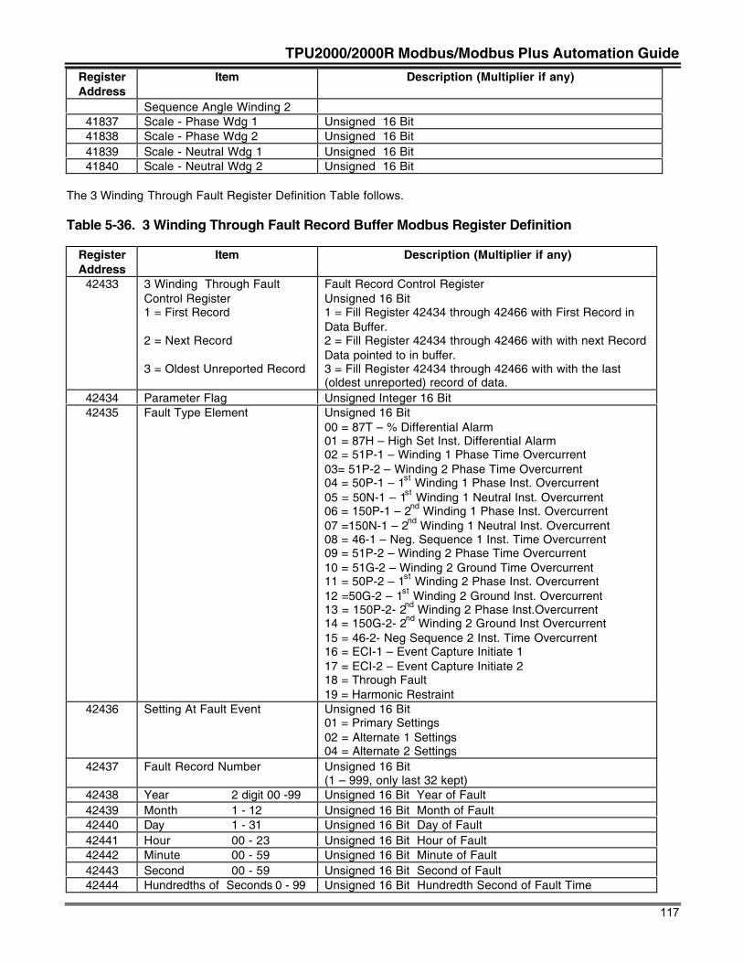
TPU2000/2000R Modbus/Modbus Plus Automation Guide
117
RegisterAddress
Item Description (Multiplier if any)
Sequence Angle Winding 241837 Scale - Phase Wdg 1 Unsigned 16 Bit41838 Scale - Phase Wdg 2 Unsigned 16 Bit41839 Scale - Neutral Wdg 1 Unsigned 16 Bit41840 Scale - Neutral Wdg 2 Unsigned 16 Bit
The 3 Winding Through Fault Register Definition Table follows.
Table 5-36. 3 Winding Through Fault Record Buffer Modbus Register Definition
RegisterAddress
Item Description (Multiplier if any)
42433 3 Winding Through FaultControl Register1 = First Record
2 = Next Record
3 = Oldest Unreported Record
Fault Record Control RegisterUnsigned 16 Bit1 = Fill Register 42434 through 42466 with First Record inData Buffer.2 = Fill Register 42434 through 42466 with with next RecordData pointed to in buffer.3 = Fill Register 42434 through 42466 with with the last(oldest unreported) record of data.
42434 Parameter Flag Unsigned Integer 16 Bit42435 Fault Type Element Unsigned 16 Bit
00 = 87T – % Differential Alarm01 = 87H – High Set Inst. Differential Alarm02 = 51P-1 – Winding 1 Phase Time Overcurrent03= 51P-2 – Winding 2 Phase Time Overcurrent04 = 50P-1 – 1st Winding 1 Phase Inst. Overcurrent05 = 50N-1 – 1st Winding 1 Neutral Inst. Overcurrent06 = 150P-1 – 2nd Winding 1 Phase Inst. Overcurrent07 =150N-1 – 2nd Winding 1 Neutral Inst. Overcurrent08 = 46-1 – Neg. Sequence 1 Inst. Time Overcurrent09 = 51P-2 – Winding 2 Phase Time Overcurrent10 = 51G-2 – Winding 2 Ground Time Overcurrent11 = 50P-2 – 1st Winding 2 Phase Inst. Overcurrent12 =50G-2 – 1st Winding 2 Ground Inst. Overcurrent13 = 150P-2- 2nd Winding 2 Phase Inst.Overcurrent14 = 150G-2- 2nd Winding 2 Ground Inst Overcurrent15 = 46-2- Neg Sequence 2 Inst. Time Overcurrent16 = ECI-1 – Event Capture Initiate 117 = ECI-2 – Event Capture Initiate 218 = Through Fault19 = Harmonic Restraint
42436 Setting At Fault Event Unsigned 16 Bit01 = Primary Settings02 = Alternate 1 Settings04 = Alternate 2 Settings
42437 Fault Record Number Unsigned 16 Bit(1 – 999, only last 32 kept)
42438 Year 2 digit 00 -99 Unsigned 16 Bit Year of Fault42439 Month 1 - 12 Unsigned 16 Bit Month of Fault42440 Day 1 - 31 Unsigned 16 Bit Day of Fault42441 Hour 00 - 23 Unsigned 16 Bit Hour of Fault42442 Minute 00 - 59 Unsigned 16 Bit Minute of Fault42443 Second 00 - 59 Unsigned 16 Bit Second of Fault42444 Hundredths of Seconds 0 - 99 Unsigned 16 Bit Hundredth Second of Fault Time
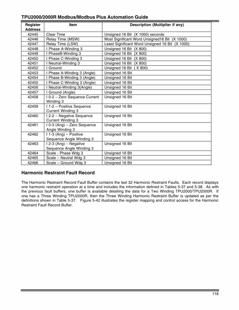
TPU2000/2000R Modbus/Modbus Plus Automation Guide
118
RegisterAddress
Item Description (Multiplier if any)
42445 Clear Time Unsigned 16 Bit (X 1000) seconds42446 Relay Time (MSW) Most Significant Word Unsigned16 Bit (X 1000)42447 Relay Time (LSW) Least Significant Word Unsigned 16 Bit (X 1000)42448 I Phase A-Winding 3 Unsigned 16 Bit (X 800)42449 I PhaseB-Winding 3 Unsigned 16 Bit (X 800)42450 I Phase C-Winding 3 Unsigned 16 Bit (X 800)42451 I Neutral-Winding 3 Unsigned 16 Bit (X 800)42452 I Ground Unsigned 16 Bit ( X 800)42453 I Phase A-Winding 3 (Angle) Unsigned 16 Bit42454 I Phase B-Winding 3 (Angle) Unsigned 16 Bit42455 I Phase C-Winding 3 (Angle) Unsigned 16 Bit42456 I Neutral-Winding 3(Angle) Unsigned 16 Bit42457 I Ground (Angle) Unsigned 16 Bit42458 I 0-2 – Zero Sequence Current
Winding 3Unsigned 16 Bit
42459 I 1-2 – Positive SequenceCurrent Winding 3
Unsigned 16 Bit
42460 I 2-2 – Negative SequenceCurrent Winding 3
Unsigned 16 Bit
42461 I 0-3 (Ang) – Zero SequenceAngle Winding 3
Unsigned 16 Bit
42462 I 1-3 (Ang) – PositiveSequence Angle Winding 3
Unsigned 16 Bit
42463 I 2-3 (Ang) – NegativeSequence Angle Winding 3
Unsigned 16 Bit
42464 Scale - Phase Wdg 3 Unsigned 16 Bit42465 Scale – Neutral Wdg 3 Unsigned 16 Bit42466 Scale – Ground Wdg 3 Unsigned 16 Bit
Harmonic Restraint Fault Record
The Harmonic Restraint Record Fault Buffer contains the last 32 Harmonic Restraint Faults. Each record displaysone harmonic restraint operation at a time and includes the information defined in Tables 5-37 and 5-38. As withthe previous fault buffers, one buffer is available detailing the data for a Two Winding TPU2000/TPU2000R. Ifone has a Three Winding TPU2000R, then the Three Winding Harmonic Restraint Buffer is updated as per thedefinitions shown in Table 5-37. Figure 5-42 illustrates the register mapping and control access for the HarmonicRestraint Fault Record Buffer.
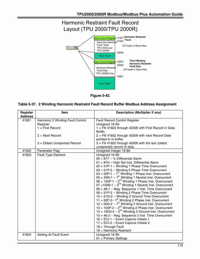
TPU2000/2000R Modbus/Modbus Plus Automation Guide
119
Harmonic Restraint Fault RecordLayout (TPU 2000/TPU 2000R)
Data Control Register
Harmonic RestraintFault DataTPU 2000 andTPU 2000R
4192141922
42009
Harmonic Restraint Fault
Data Control Register
Harmonic Restraint Fault Data TPU 2000R Only
4256142562
42601
32 Faults in Stack Max..
32 Faults in Stack Max.
Fault Stack
Fault Stack
Third Winding Harmonic RestraintFault Data
EC
Figure 5-42.
Table 5-37. 2 Winding Harmonic Restraint Fault Record Buffer Modbus Address Assignment
RegisterAddress
Item Description (Multiplier if any)
41921 Harmonic 2 Winding Fault ControlRegister1 = First Record
2 = Next Record
3 = Oldest Unreported Record
Fault Record Control RegisterUnsigned 16 Bit1 = Fill 41922 through 42009 with First Record in DataBuffer.2 = Fill 41922 through 42009 with next Record Datapointed to in buffer.3 = Fill 41922 through 42009 with the last (oldestunreported) record of data.
41922 Parameter Flag Unsigned Integer 16 Bit41923 Fault Type Element Unsigned 16 Bit
00 = 87T – % Differential Alarm01 = 87H – High Set Inst. Differential Alarm02 = 51P-1 – Winding 1 Phase Time Overcurrent03 = 51P-2 – Winding 2 Phase Time Overcurrent04 = 50P-1 – 1st Winding 1 Phase Inst. Overcurrent05 = 50N-1 – 1st Winding 1 Neutral Inst. Overcurrent06 = 150P-1 – 2nd Winding 1 Phase Inst. Overcurrent07 =150N-1 – 2nd Winding 1 Neutral Inst. Overcurrent08 = 46-1 – Neg. Sequence 1 Inst. Time Overcurrent09 = 51P-2 – Winding 2 Phase Time Overcurrent10 = 51G-2 – Winding 2 Ground Time Overcurrent11 = 50P-2– 1st Winding 2 Phase Inst. Overcurrent12 = 50G-2 – 1st Winding 2 Ground Inst. Overcurrent13 = 150P-2 – 2nd Winding 2 Phase Inst. Overcurrent14 = 150G-2 – 2nd Winding 2 Ground Inst. Overcurrent15 = 46-2 – Neg. Sequence 2 Inst. Time Overcurrent16 = ECI-1 – Event Capture Initiate 117 = ECI-2 – Event Capture Initiate 218 = Through Fault19 = Harmonic Restraint
41924 Setting At Fault Event Unsigned 16 Bit01 = Primary Settings
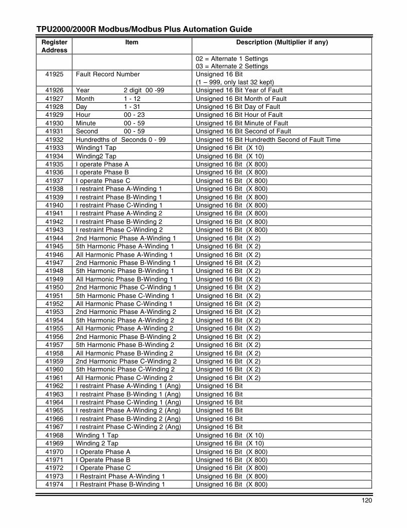
TPU2000/2000R Modbus/Modbus Plus Automation Guide
120
RegisterAddress
Item Description (Multiplier if any)
02 = Alternate 1 Settings03 = Alternate 2 Settings
41925 Fault Record Number Unsigned 16 Bit(1 – 999, only last 32 kept)
41926 Year 2 digit 00 -99 Unsigned 16 Bit Year of Fault41927 Month 1 - 12 Unsigned 16 Bit Month of Fault41928 Day 1 - 31 Unsigned 16 Bit Day of Fault41929 Hour 00 - 23 Unsigned 16 Bit Hour of Fault41930 Minute 00 - 59 Unsigned 16 Bit Minute of Fault41931 Second 00 - 59 Unsigned 16 Bit Second of Fault41932 Hundredths of Seconds 0 - 99 Unsigned 16 Bit Hundredth Second of Fault Time41933 Winding1 Tap Unsigned 16 Bit (X 10)41934 Winding2 Tap Unsigned 16 Bit (X 10)41935 I operate Phase A Unsigned 16 Bit (X 800)41936 I operate Phase B Unsigned 16 Bit (X 800)41937 I operate Phase C Unsigned 16 Bit (X 800)41938 I restraint Phase A-Winding 1 Unsigned 16 Bit (X 800)41939 I restraint Phase B-Winding 1 Unsigned 16 Bit (X 800)41940 I restraint Phase C-Winding 1 Unsigned 16 Bit (X 800)41941 I restraint Phase A-Winding 2 Unsigned 16 Bit (X 800)41942 I restraint Phase B-Winding 2 Unsigned 16 Bit (X 800)41943 I restraint Phase C-Winding 2 Unsigned 16 Bit (X 800)41944 2nd Harmonic Phase A-Winding 1 Unsigned 16 Bit (X 2)41945 5th Harmonic Phase A-Winding 1 Unsigned 16 Bit (X 2)41946 All Harmonic Phase A-Winding 1 Unsigned 16 Bit (X 2)41947 2nd Harmonic Phase B-Winding 1 Unsigned 16 Bit (X 2)41948 5th Harmonic Phase B-Winding 1 Unsigned 16 Bit (X 2)41949 All Harmonic Phase B-Winding 1 Unsigned 16 Bit (X 2)41950 2nd Harmonic Phase C-Winding 1 Unsigned 16 Bit (X 2)41951 5th Harmonic Phase C-Winding 1 Unsigned 16 Bit (X 2)41952 All Harmonic Phase C-Winding 1 Unsigned 16 Bit (X 2)41953 2nd Harmonic Phase A-Winding 2 Unsigned 16 Bit (X 2)41954 5th Harmonic Phase A-Winding 2 Unsigned 16 Bit (X 2)41955 All Harmonic Phase A-Winding 2 Unsigned 16 Bit (X 2)41956 2nd Harmonic Phase B-Winding 2 Unsigned 16 Bit (X 2)41957 5th Harmonic Phase B-Winding 2 Unsigned 16 Bit (X 2)41958 All Harmonic Phase B-Winding 2 Unsigned 16 Bit (X 2)41959 2nd Harmonic Phase C-Winding 2 Unsigned 16 Bit (X 2)41960 5th Harmonic Phase C-Winding 2 Unsigned 16 Bit (X 2)41961 All Harmonic Phase C-Winding 2 Unsigned 16 Bit (X 2)41962 I restraint Phase A-Winding 1 (Ang) Unsigned 16 Bit41963 I restraint Phase B-Winding 1 (Ang) Unsigned 16 Bit41964 I restraint Phase C-Winding 1 (Ang) Unsigned 16 Bit41965 I restraint Phase A-Winding 2 (Ang) Unsigned 16 Bit41966 I restraint Phase B-Winding 2 (Ang) Unsigned 16 Bit41967 I restraint Phase C-Winding 2 (Ang) Unsigned 16 Bit41968 Winding 1 Tap Unsigned 16 Bit (X 10)41969 Winding 2 Tap Unsigned 16 Bit (X 10)41970 I Operate Phase A Unsigned 16 Bit (X 800)41971 I Operate Phase B Unsigned 16 Bit (X 800)41972 I Operate Phase C Unsigned 16 Bit (X 800)41973 I Restraint Phase A-Winding 1 Unsigned 16 Bit (X 800)41974 I Restraint Phase B-Winding 1 Unsigned 16 Bit (X 800)
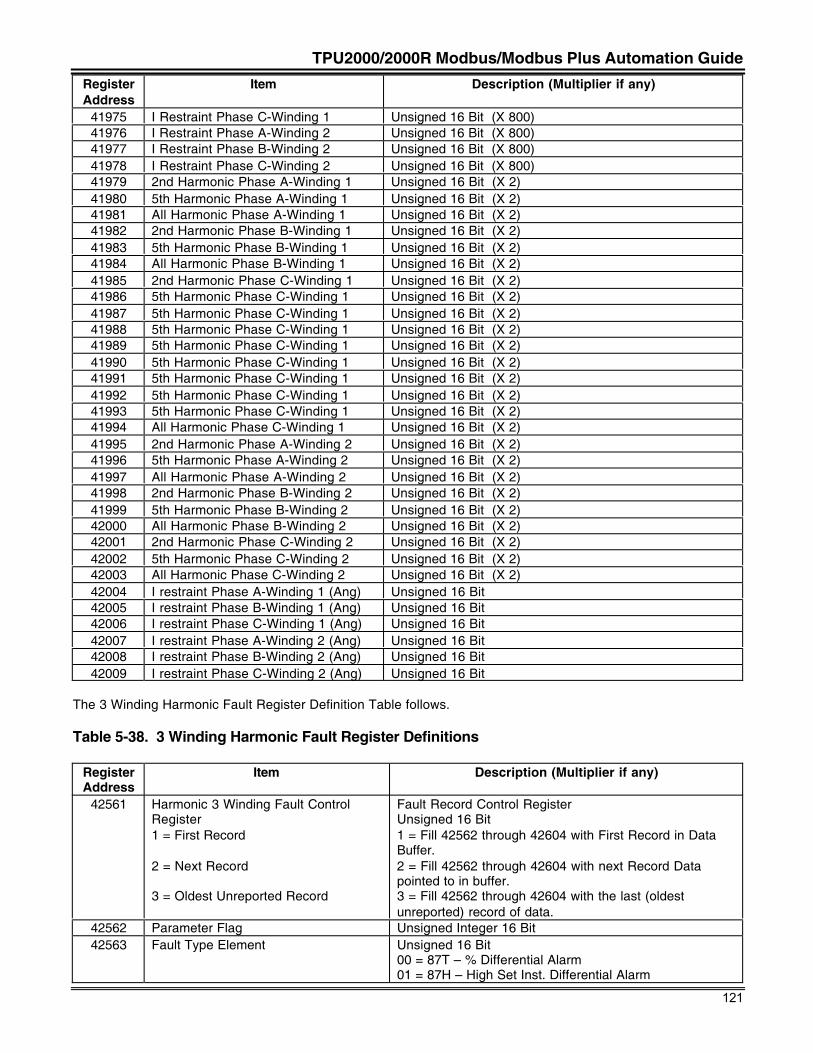
TPU2000/2000R Modbus/Modbus Plus Automation Guide
121
RegisterAddress
Item Description (Multiplier if any)
41975 I Restraint Phase C-Winding 1 Unsigned 16 Bit (X 800)41976 I Restraint Phase A-Winding 2 Unsigned 16 Bit (X 800)41977 I Restraint Phase B-Winding 2 Unsigned 16 Bit (X 800)41978 I Restraint Phase C-Winding 2 Unsigned 16 Bit (X 800)41979 2nd Harmonic Phase A-Winding 1 Unsigned 16 Bit (X 2)41980 5th Harmonic Phase A-Winding 1 Unsigned 16 Bit (X 2)41981 All Harmonic Phase A-Winding 1 Unsigned 16 Bit (X 2)41982 2nd Harmonic Phase B-Winding 1 Unsigned 16 Bit (X 2)41983 5th Harmonic Phase B-Winding 1 Unsigned 16 Bit (X 2)41984 All Harmonic Phase B-Winding 1 Unsigned 16 Bit (X 2)41985 2nd Harmonic Phase C-Winding 1 Unsigned 16 Bit (X 2)41986 5th Harmonic Phase C-Winding 1 Unsigned 16 Bit (X 2)41987 5th Harmonic Phase C-Winding 1 Unsigned 16 Bit (X 2)41988 5th Harmonic Phase C-Winding 1 Unsigned 16 Bit (X 2)41989 5th Harmonic Phase C-Winding 1 Unsigned 16 Bit (X 2)41990 5th Harmonic Phase C-Winding 1 Unsigned 16 Bit (X 2)41991 5th Harmonic Phase C-Winding 1 Unsigned 16 Bit (X 2)41992 5th Harmonic Phase C-Winding 1 Unsigned 16 Bit (X 2)41993 5th Harmonic Phase C-Winding 1 Unsigned 16 Bit (X 2)41994 All Harmonic Phase C-Winding 1 Unsigned 16 Bit (X 2)41995 2nd Harmonic Phase A-Winding 2 Unsigned 16 Bit (X 2)41996 5th Harmonic Phase A-Winding 2 Unsigned 16 Bit (X 2)41997 All Harmonic Phase A-Winding 2 Unsigned 16 Bit (X 2)41998 2nd Harmonic Phase B-Winding 2 Unsigned 16 Bit (X 2)41999 5th Harmonic Phase B-Winding 2 Unsigned 16 Bit (X 2)42000 All Harmonic Phase B-Winding 2 Unsigned 16 Bit (X 2)42001 2nd Harmonic Phase C-Winding 2 Unsigned 16 Bit (X 2)42002 5th Harmonic Phase C-Winding 2 Unsigned 16 Bit (X 2)42003 All Harmonic Phase C-Winding 2 Unsigned 16 Bit (X 2)42004 I restraint Phase A-Winding 1 (Ang) Unsigned 16 Bit42005 I restraint Phase B-Winding 1 (Ang) Unsigned 16 Bit42006 I restraint Phase C-Winding 1 (Ang) Unsigned 16 Bit42007 I restraint Phase A-Winding 2 (Ang) Unsigned 16 Bit42008 I restraint Phase B-Winding 2 (Ang) Unsigned 16 Bit42009 I restraint Phase C-Winding 2 (Ang) Unsigned 16 Bit
The 3 Winding Harmonic Fault Register Definition Table follows.
Table 5-38. 3 Winding Harmonic Fault Register Definitions
RegisterAddress
Item Description (Multiplier if any)
42561 Harmonic 3 Winding Fault ControlRegister1 = First Record
2 = Next Record
3 = Oldest Unreported Record
Fault Record Control RegisterUnsigned 16 Bit1 = Fill 42562 through 42604 with First Record in DataBuffer.2 = Fill 42562 through 42604 with next Record Datapointed to in buffer.3 = Fill 42562 through 42604 with the last (oldestunreported) record of data.
42562 Parameter Flag Unsigned Integer 16 Bit42563 Fault Type Element Unsigned 16 Bit
00 = 87T – % Differential Alarm01 = 87H – High Set Inst. Differential Alarm
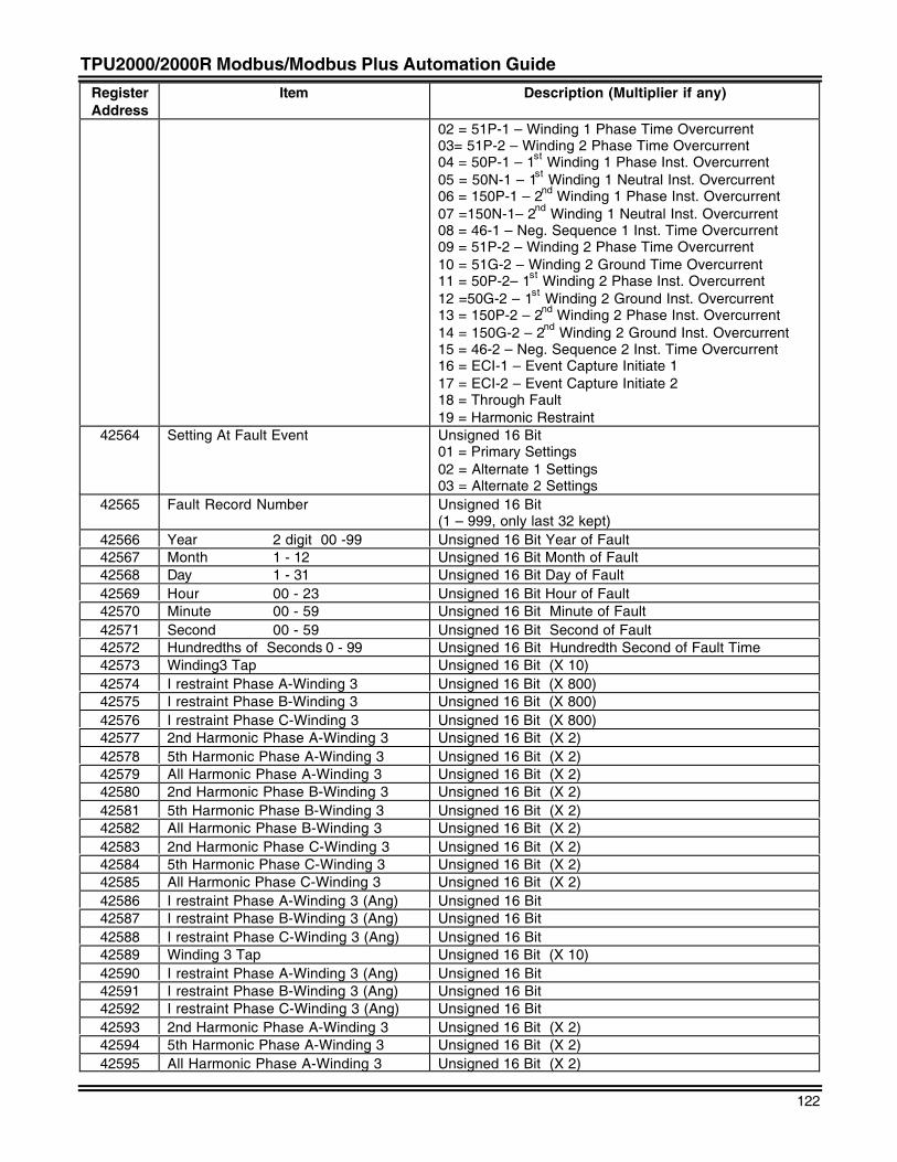
TPU2000/2000R Modbus/Modbus Plus Automation Guide
122
RegisterAddress
Item Description (Multiplier if any)
02 = 51P-1 – Winding 1 Phase Time Overcurrent03= 51P-2 – Winding 2 Phase Time Overcurrent04 = 50P-1 – 1st Winding 1 Phase Inst. Overcurrent05 = 50N-1 – 1st Winding 1 Neutral Inst. Overcurrent06 = 150P-1 – 2nd Winding 1 Phase Inst. Overcurrent07 =150N-1– 2nd Winding 1 Neutral Inst. Overcurrent08 = 46-1 – Neg. Sequence 1 Inst. Time Overcurrent09 = 51P-2 – Winding 2 Phase Time Overcurrent10 = 51G-2 – Winding 2 Ground Time Overcurrent11 = 50P-2– 1st Winding 2 Phase Inst. Overcurrent12 =50G-2 – 1st Winding 2 Ground Inst. Overcurrent13 = 150P-2 – 2nd Winding 2 Phase Inst. Overcurrent14 = 150G-2 – 2nd Winding 2 Ground Inst. Overcurrent15 = 46-2 – Neg. Sequence 2 Inst. Time Overcurrent16 = ECI-1 – Event Capture Initiate 117 = ECI-2 – Event Capture Initiate 218 = Through Fault19 = Harmonic Restraint
42564 Setting At Fault Event Unsigned 16 Bit01 = Primary Settings02 = Alternate 1 Settings03 = Alternate 2 Settings
42565 Fault Record Number Unsigned 16 Bit(1 – 999, only last 32 kept)
42566 Year 2 digit 00 -99 Unsigned 16 Bit Year of Fault42567 Month 1 - 12 Unsigned 16 Bit Month of Fault42568 Day 1 - 31 Unsigned 16 Bit Day of Fault42569 Hour 00 - 23 Unsigned 16 Bit Hour of Fault42570 Minute 00 - 59 Unsigned 16 Bit Minute of Fault42571 Second 00 - 59 Unsigned 16 Bit Second of Fault42572 Hundredths of Seconds 0 - 99 Unsigned 16 Bit Hundredth Second of Fault Time42573 Winding3 Tap Unsigned 16 Bit (X 10)42574 I restraint Phase A-Winding 3 Unsigned 16 Bit (X 800)42575 I restraint Phase B-Winding 3 Unsigned 16 Bit (X 800)42576 I restraint Phase C-Winding 3 Unsigned 16 Bit (X 800)42577 2nd Harmonic Phase A-Winding 3 Unsigned 16 Bit (X 2)42578 5th Harmonic Phase A-Winding 3 Unsigned 16 Bit (X 2)42579 All Harmonic Phase A-Winding 3 Unsigned 16 Bit (X 2)42580 2nd Harmonic Phase B-Winding 3 Unsigned 16 Bit (X 2)42581 5th Harmonic Phase B-Winding 3 Unsigned 16 Bit (X 2)42582 All Harmonic Phase B-Winding 3 Unsigned 16 Bit (X 2)42583 2nd Harmonic Phase C-Winding 3 Unsigned 16 Bit (X 2)42584 5th Harmonic Phase C-Winding 3 Unsigned 16 Bit (X 2)42585 All Harmonic Phase C-Winding 3 Unsigned 16 Bit (X 2)42586 I restraint Phase A-Winding 3 (Ang) Unsigned 16 Bit42587 I restraint Phase B-Winding 3 (Ang) Unsigned 16 Bit42588 I restraint Phase C-Winding 3 (Ang) Unsigned 16 Bit42589 Winding 3 Tap Unsigned 16 Bit (X 10)42590 I restraint Phase A-Winding 3 (Ang) Unsigned 16 Bit42591 I restraint Phase B-Winding 3 (Ang) Unsigned 16 Bit42592 I restraint Phase C-Winding 3 (Ang) Unsigned 16 Bit42593 2nd Harmonic Phase A-Winding 3 Unsigned 16 Bit (X 2)42594 5th Harmonic Phase A-Winding 3 Unsigned 16 Bit (X 2)42595 All Harmonic Phase A-Winding 3 Unsigned 16 Bit (X 2)
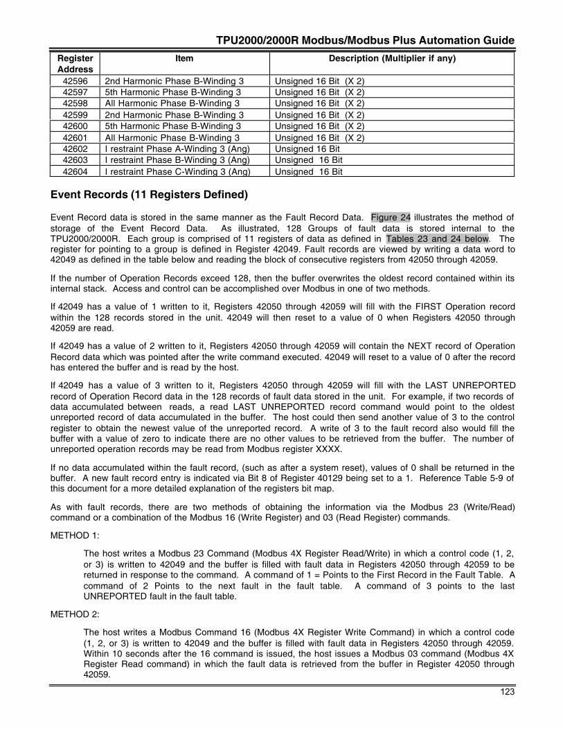
TPU2000/2000R Modbus/Modbus Plus Automation Guide
123
RegisterAddress
Item Description (Multiplier if any)
42596 2nd Harmonic Phase B-Winding 3 Unsigned 16 Bit (X 2)42597 5th Harmonic Phase B-Winding 3 Unsigned 16 Bit (X 2)42598 All Harmonic Phase B-Winding 3 Unsigned 16 Bit (X 2)42599 2nd Harmonic Phase B-Winding 3 Unsigned 16 Bit (X 2)42600 5th Harmonic Phase B-Winding 3 Unsigned 16 Bit (X 2)42601 All Harmonic Phase B-Winding 3 Unsigned 16 Bit (X 2)42602 I restraint Phase A-Winding 3 (Ang) Unsigned 16 Bit42603 I restraint Phase B-Winding 3 (Ang) Unsigned 16 Bit42604 I restraint Phase C-Winding 3 (Ang) Unsigned 16 Bit
Event Records (11 Registers Defined)
Event Record data is stored in the same manner as the Fault Record Data. Figure 24 illustrates the method ofstorage of the Event Record Data. As illustrated, 128 Groups of fault data is stored internal to theTPU2000/2000R. Each group is comprised of 11 registers of data as defined in Tables 23 and 24 below. Theregister for pointing to a group is defined in Register 42049. Fault records are viewed by writing a data word to42049 as defined in the table below and reading the block of consecutive registers from 42050 through 42059.
If the number of Operation Records exceed 128, then the buffer overwrites the oldest record contained within itsinternal stack. Access and control can be accomplished over Modbus in one of two methods.
If 42049 has a value of 1 written to it, Registers 42050 through 42059 will fill with the FIRST Operation recordwithin the 128 records stored in the unit. 42049 will then reset to a value of 0 when Registers 42050 through42059 are read.
If 42049 has a value of 2 written to it, Registers 42050 through 42059 will contain the NEXT record of OperationRecord data which was pointed after the write command executed. 42049 will reset to a value of 0 after the recordhas entered the buffer and is read by the host.
If 42049 has a value of 3 written to it, Registers 42050 through 42059 will fill with the LAST UNREPORTEDrecord of Operation Record data in the 128 records of fault data stored in the unit. For example, if two records ofdata accumulated between reads, a read LAST UNREPORTED record command would point to the oldestunreported record of data accumulated in the buffer. The host could then send another value of 3 to the controlregister to obtain the newest value of the unreported record. A write of 3 to the fault record also would fill thebuffer with a value of zero to indicate there are no other values to be retrieved from the buffer. The number ofunreported operation records may be read from Modbus register XXXX.
If no data accumulated within the fault record, (such as after a system reset), values of 0 shall be returned in thebuffer. A new fault record entry is indicated via Bit 8 of Register 40129 being set to a 1. Reference Table 5-9 ofthis document for a more detailed explanation of the registers bit map.
As with fault records, there are two methods of obtaining the information via the Modbus 23 (Write/Read)command or a combination of the Modbus 16 (Write Register) and 03 (Read Register) commands.
METHOD 1:
The host writes a Modbus 23 Command (Modbus 4X Register Read/Write) in which a control code (1, 2,or 3) is written to 42049 and the buffer is filled with fault data in Registers 42050 through 42059 to bereturned in response to the command. A command of 1 = Points to the First Record in the Fault Table. Acommand of 2 Points to the next fault in the fault table. A command of 3 points to the lastUNREPORTED fault in the fault table.
METHOD 2:
The host writes a Modbus Command 16 (Modbus 4X Register Write Command) in which a control code(1, 2, or 3) is written to 42049 and the buffer is filled with fault data in Registers 42050 through 42059.Within 10 seconds after the 16 command is issued, the host issues a Modbus 03 command (Modbus 4XRegister Read command) in which the fault data is retrieved from the buffer in Register 42050 through42059.
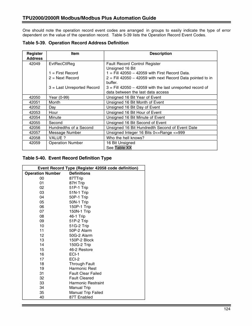
TPU2000/2000R Modbus/Modbus Plus Automation Guide
124
One should note the operation record event codes are arranged in groups to easily indicate the type of errordependent on the value of the operation record. Table 5-39 lists the Operation Record Event Codes.
Table 5-39. Operation Record Address Definition
RegisterAddress
Item Description
42049 EvtRecCtlReg
1 = First Record2 = Next Record
3 = Last Unreported Record
Fault Record Control RegisterUnsigned 16 Bit1 = Fill 42050 – 42059 with First Record Data.2 = Fill 42050 – 42059 with next Record Data pointed to inbuffer.3 = Fill 42050 – 42059 with the last unreported record ofdata between the last data access
42050 Year (0-99) Unsigned 16 Bit Year of Event42051 Month Unsigned 16 Bit Month of Event42052 Day Unsigned 16 Bit Day of Event42053 Hour Unsigned 16 Bit Hour of Event42054 Minute Unsigned 16 Bit Minute of Event42055 Second Unsigned 16 Bit Second of Event42056 Hundredths of a Second Unsigned 16 Bit Hundredth Second of Event Date42057 Message Number Unsigned Integer 16 Bits 0<=Range <=99942058 VALUE ? Who the hell knows?42059 Operation Number 16 Bit Unsigned
See Table XX
Table 5-40. Event Record Definition Type
Event Record Type (Register 42058 code definition)Operation Number Definitions
00 87TTrip01 87H Trip02 51P-1 Trip03 51N-1 Trip04 50P-1 Trip05 50N-1 Trip06 150P-1 Trip07 150N-1 Trip08 46-1 Trip09 51P-2 Trip10 51G-2 Trip11 50P-2 Alarm12 50G-2 Alarm13 150P-2 Block14 150G-2 Trip15 46-2 Restore16 ECI-117 ECI-218 Through Fault19 Harmonic Rest31 Fault Clear Failed32 Fault Cleared33 Harmonic Restraint34 Manual Trip35 Manual Trip Failed40 87T Enabled
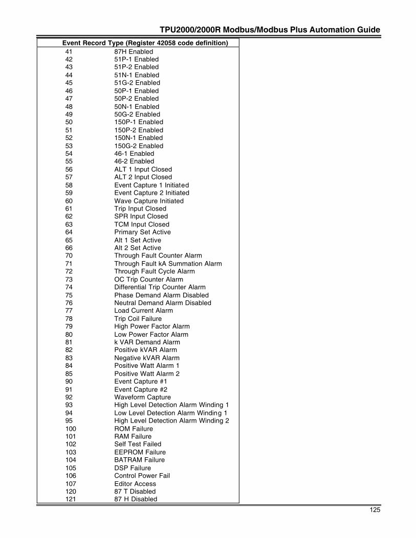
TPU2000/2000R Modbus/Modbus Plus Automation Guide
125
Event Record Type (Register 42058 code definition)41 87H Enabled42 51P-1 Enabled43 51P-2 Enabled44 51N-1 Enabled45 51G-2 Enabled46 50P-1 Enabled47 50P-2 Enabled48 50N-1 Enabled49 50G-2 Enabled50 150P-1 Enabled51 150P-2 Enabled52 150N-1 Enabled53 150G-2 Enabled54 46-1 Enabled55 46-2 Enabled56 ALT 1 Input Closed57 ALT 2 Input Closed58 Event Capture 1 Initiated59 Event Capture 2 Initiated60 Wave Capture Initiated61 Trip Input Closed62 SPR Input Closed63 TCM Input Closed64 Primary Set Active65 Alt 1 Set Active66 Alt 2 Set Active70 Through Fault Counter Alarm71 Through Fault kA Summation Alarm72 Through Fault Cycle Alarm73 OC Trip Counter Alarm74 Differential Trip Counter Alarm75 Phase Demand Alarm Disabled76 Neutral Demand Alarm Disabled77 Load Current Alarm78 Trip Coil Failure79 High Power Factor Alarm80 Low Power Factor Alarm81 k VAR Demand Alarm82 Positive kVAR Alarm83 Negative kVAR Alarm84 Positive Watt Alarm 185 Positive Watt Alarm 290 Event Capture #191 Event Capture #292 Waveform Capture93 High Level Detection Alarm Winding 194 Low Level Detection Alarm Winding 195 High Level Detection Alarm Winding 2100 ROM Failure101 RAM Failure102 Self Test Failed103 EEPROM Failure104 BATRAM Failure105 DSP Failure106 Control Power Fail107 Editor Access120 87 T Disabled121 87 H Disabled
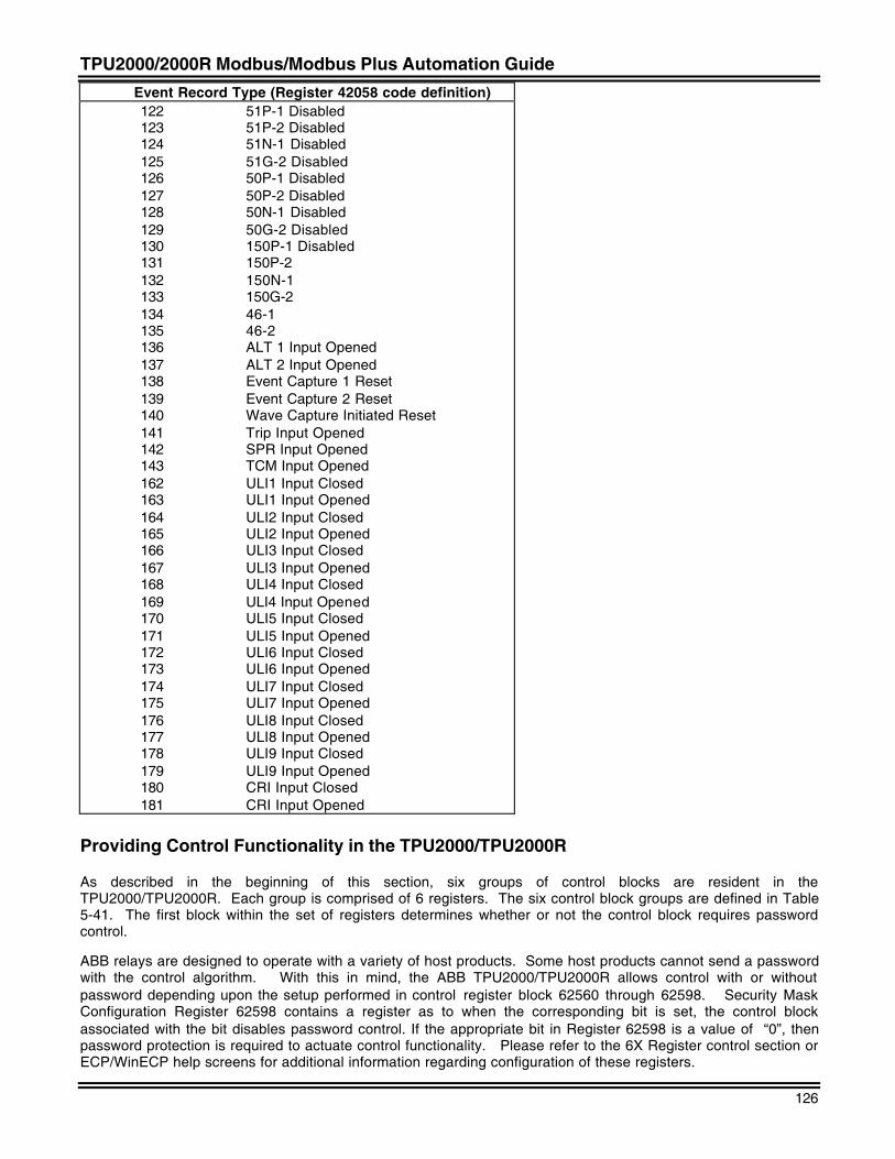
TPU2000/2000R Modbus/Modbus Plus Automation Guide
126
Event Record Type (Register 42058 code definition)122 51P-1 Disabled123 51P-2 Disabled124 51N-1 Disabled125 51G-2 Disabled126 50P-1 Disabled127 50P-2 Disabled128 50N-1 Disabled129 50G-2 Disabled130 150P-1 Disabled131 150P-2132 150N-1133 150G-2134 46-1135 46-2136 ALT 1 Input Opened137 ALT 2 Input Opened138 Event Capture 1 Reset139 Event Capture 2 Reset140 Wave Capture Initiated Reset141 Trip Input Opened142 SPR Input Opened143 TCM Input Opened162 ULI1 Input Closed163 ULI1 Input Opened164 ULI2 Input Closed165 ULI2 Input Opened166 ULI3 Input Closed167 ULI3 Input Opened168 ULI4 Input Closed169 ULI4 Input Opened170 ULI5 Input Closed171 ULI5 Input Opened172 ULI6 Input Closed173 ULI6 Input Opened174 ULI7 Input Closed175 ULI7 Input Opened176 ULI8 Input Closed177 ULI8 Input Opened178 ULI9 Input Closed179 ULI9 Input Opened180 CRI Input Closed181 CRI Input Opened
Providing Control Functionality in the TPU2000/TPU2000R
As described in the beginning of this section, six groups of control blocks are resident in theTPU2000/TPU2000R. Each group is comprised of 6 registers. The six control block groups are defined in Table5-41. The first block within the set of registers determines whether or not the control block requires passwordcontrol.
ABB relays are designed to operate with a variety of host products. Some host products cannot send a passwordwith the control algorithm. With this in mind, the ABB TPU2000/TPU2000R allows control with or withoutpassword depending upon the setup performed in control register block 62560 through 62598. Security MaskConfiguration Register 62598 contains a register as to when the corresponding bit is set, the control blockassociated with the bit disables password control. If the appropriate bit in Register 62598 is a value of “0”, thenpassword protection is required to actuate control functionality. Please refer to the 6X Register control section orECP/WinECP help screens for additional information regarding configuration of these registers.
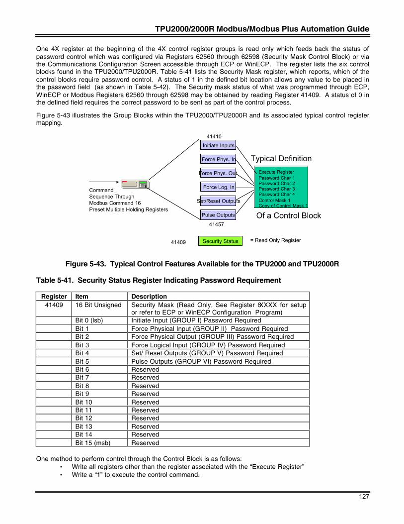
TPU2000/2000R Modbus/Modbus Plus Automation Guide
127
One 4X register at the beginning of the 4X control register groups is read only which feeds back the status ofpassword control which was configured via Registers 62560 through 62598 (Security Mask Control Block) or viathe Communications Configuration Screen accessible through ECP or WinECP. The register lists the six controlblocks found in the TPU2000/TPU2000R. Table 5-41 lists the Security Mask register, which reports, which of thecontrol blocks require password control. A status of 1 in the defined bit location allows any value to be placed inthe password field (as shown in Table 5-42). The Security mask status of what was programmed through ECP,WinECP or Modbus Registers 62560 through 62598 may be obtained by reading Register 41409. A status of 0 inthe defined field requires the correct password to be sent as part of the control process.
Figure 5-43 illustrates the Group Blocks within the TPU2000/TPU2000R and its associated typical control registermapping.
Execute RegisterPassword Char 1Password Char 2Password Char 3Password Char 4Control Mask 1Copy of Control Mask 1
Initiate Inputs
Force Phys. In
Force Phys. Out.
Force Log. In
Set/Reset Outputs
Pulse Outputs
Typical Definition
EC
Of a Control Block
CommandSequence ThroughModbus Command 16Preset Multiple Holding Registers
Security Status = Read Only Register41409
41410
41457
Figure 5-43. Typical Control Features Available for the TPU2000 and TPU2000R
Table 5-41. Security Status Register Indicating Password Requirement
Register Item Description41409 16 Bit Unsigned Security Mask (Read Only, See Register 6XXXX for setup
or refer to ECP or WinECP Configuration Program)Bit 0 (lsb) Initiate Input (GROUP I) Password RequiredBit 1 Force Physical Input (GROUP II) Password RequiredBit 2 Force Physical Output (GROUP III) Password RequiredBit 3 Force Logical Input (GROUP IV) Password RequiredBit 4 Set/ Reset Outputs (GROUP V) Password RequiredBit 5 Pulse Outputs (GROUP VI) Password RequiredBit 6 ReservedBit 7 ReservedBit 8 ReservedBit 9 ReservedBit 10 ReservedBit 11 ReservedBit 12 ReservedBit 13 ReservedBit 14 ReservedBit 15 (msb) Reserved
One method to perform control through the Control Block is as follows:• Write all registers other than the register associated with the “Execute Register”• Write a “1” to execute the control command.
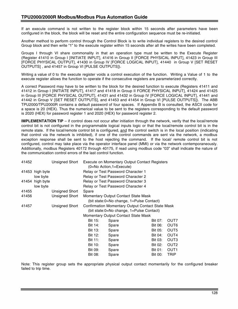
TPU2000/2000R Modbus/Modbus Plus Automation Guide
128
If an execute command is not written to the register block within 15 seconds after parameters have beenconfigured in the block, the block will be reset and the entire configuration sequence must be re-initiated.
Another method to perform control through the Control Block is to write individual registers to the desired controlGroup block and then write “1” to the execute register within 15 seconds after all the writes have been completed.
Groups I through VI share commonality in that an operation type must be written to the Execute Register(Register 41410 in Group I [INITIATE INPUT], 41416 in Group II [FORCE PHYSICAL INPUT], 41423 in Group III[FORCE PHYSICAL OUTPUT], 41430 in Group IV [FORCE LOGICAL INPUT], 41440 in Group V [SET RESETOUTPUTS] , and 41457 in Group VI [PULSE OUTPUTS]).
Writing a value of 0 to the execute register voids a control execution of the function. Writing a Value of 1 to theexecute register allows the function to operate if the consecutive registers are parameterized correctly.
A correct Password may have to be written to the block for the desired function to execute (Registers 41411 and41412 in Group I [INITIATE INPUT], 41417 and 41418 in Group II FORCE PHYSICAL INPUT], 41424 and 41425in Group III [FORCE PHYSICAL OUTPUT], 41431 and 41432 in Group IV [FORCE LOGICAL INPUT], 41441 and41442 in Group V [SET RESET OUTPUTS], and 41453 and 41454 in Group VI [PULSE OUTPUTS]). The ABBTPU2000/TPU2000R contains a default password of four spaces. If Appendix B is consulted, the ASCII code fora space is 20 (HEX). Thus the numerical value to be sent to the registers corresponding to the default passwordis 2020 (HEX) for password register 1 and 2020 (HEX) for password register 2.
IMPLEMENTATION TIP – if control does not occur after initiation through the network, verify that the local/remotecontrol bit is not configured in the programmable logical inputs logic or that the local/remote control bit is in theremote state. If the local/remote control bit is configured, and the control switch is in the local position (indicatingthat control via the network is inhibited), if one of the control commands are sent via the network, a modbusexception response shall be sent to the host rejecting the command. If the local/ remote control bit is notconfigured, control may take place via the operator interface panel (MMI) or via the network contemporaneously.Additionally, modbus Registers 40172 through 40175, if read using modbus code “03” shall indicate the nature ofthe communication control errors of the last control function.
41452 Unsigned Short Execute on Momentary Output Contact Registers(0=No Action,1=Execute)
41453 high byte Relay or Test Password Character 1low byte Relay or Test Password Character 2
41454 high byte Relay or Test Password Character 3low byte Relay or Test Password Character 4
41455 Unsigned Short Spare41456 Unsigned Short Momentary Output Contact State Mask
(bit state:0=No change, 1=Pulse Contact)41457 Unsigned Short Confirmation Momentary Output Contact State Mask
(bit state:0=No change, 1=Pulse Contact)Momentary Output Contact State Mask
Bit 15: Spare Bit 07: OUT7Bit 14: Spare Bit 06: OUT6Bit 13: Spare Bit 05: OUT5Bit 12: Spare Bit 04: OUT4Bit 11: Spare Bit 03: OUT3Bit 10: Spare Bit 02: OUT2Bit 09: Spare Bit 01: OUT1Bit 08: Spare Bit 00: TRIP
Note: This register group sets the appropriate physical output contact momentarily for the configured breakerfailed to trip time.
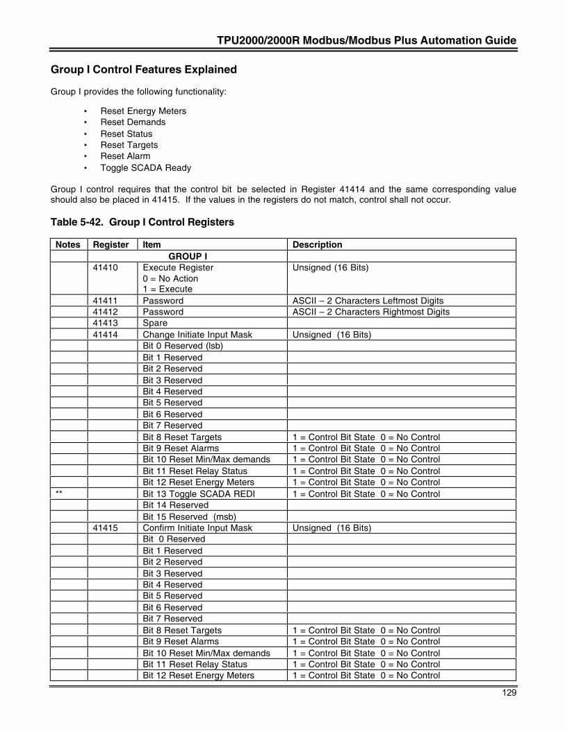
TPU2000/2000R Modbus/Modbus Plus Automation Guide
129
Group I Control Features Explained
Group I provides the following functionality:
• Reset Energy Meters• Reset Demands• Reset Status• Reset Targets• Reset Alarm• Toggle SCADA Ready
Group I control requires that the control bit be selected in Register 41414 and the same corresponding valueshould also be placed in 41415. If the values in the registers do not match, control shall not occur.
Table 5-42. Group I Control Registers
Notes Register Item DescriptionGROUP I
41410 Execute Register0 = No Action1 = Execute
Unsigned (16 Bits)
41411 Password ASCII – 2 Characters Leftmost Digits41412 Password ASCII – 2 Characters Rightmost Digits41413 Spare41414 Change Initiate Input Mask Unsigned (16 Bits)
Bit 0 Reserved (lsb)Bit 1 ReservedBit 2 ReservedBit 3 ReservedBit 4 ReservedBit 5 ReservedBit 6 ReservedBit 7 ReservedBit 8 Reset Targets 1 = Control Bit State 0 = No ControlBit 9 Reset Alarms 1 = Control Bit State 0 = No ControlBit 10 Reset Min/Max demands 1 = Control Bit State 0 = No ControlBit 11 Reset Relay Status 1 = Control Bit State 0 = No ControlBit 12 Reset Energy Meters 1 = Control Bit State 0 = No Control
** Bit 13 Toggle SCADA REDI 1 = Control Bit State 0 = No ControlBit 14 ReservedBit 15 Reserved (msb)
41415 Confirm Initiate Input Mask Unsigned (16 Bits)Bit 0 ReservedBit 1 ReservedBit 2 ReservedBit 3 ReservedBit 4 ReservedBit 5 ReservedBit 6 ReservedBit 7 ReservedBit 8 Reset Targets 1 = Control Bit State 0 = No ControlBit 9 Reset Alarms 1 = Control Bit State 0 = No ControlBit 10 Reset Min/Max demands 1 = Control Bit State 0 = No ControlBit 11 Reset Relay Status 1 = Control Bit State 0 = No ControlBit 12 Reset Energy Meters 1 = Control Bit State 0 = No Control
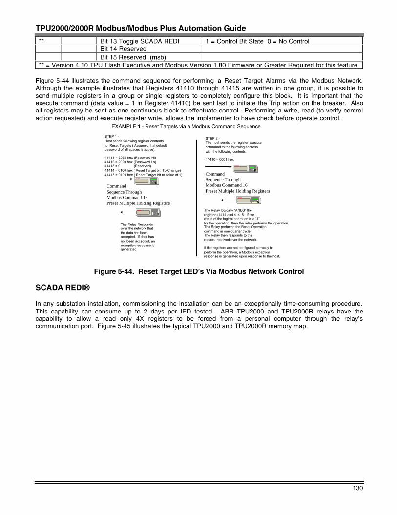
TPU2000/2000R Modbus/Modbus Plus Automation Guide
130
** Bit 13 Toggle SCADA REDI 1 = Control Bit State 0 = No ControlBit 14 ReservedBit 15 Reserved (msb)
** = Version 4.10 TPU Flash Executive and Modbus Version 1.80 Firmware or Greater Required for this feature
Figure 5-44 illustrates the command sequence for performing a Reset Target Alarms via the Modbus Network.Although the example illustrates that Registers 41410 through 41415 are written in one group, it is possible tosend multiple registers in a group or single registers to completely configure this block. It is important that theexecute command (data value = 1 in Register 41410) be sent last to initiate the Trip action on the breaker. Alsoall registers may be sent as one continuous block to effectuate control. Performing a write, read (to verify controlaction requested) and execute register write, allows the implementer to have check before operate control.
EC
CommandSequence ThroughModbus Command 16Preset Multiple Holding Registers
STEP 1 -Host sends following register contentsto Reset Targets ( Assumed that defaultpassword of all spaces is active).
41411 = 2020 hex (Password Hi)41412 = 2020 hex (Password Lo)41413 = 0 (Reserved)41414 = 0100 hex ( Reset Target bit To Change)41415 = 0100 hex ( Reset Target bit to value of 1).
EXAMPLE 1 - Reset Targets via a Modbus Command Sequence.
EC
The Relay logically “ANDS” the register 41414 and 41415. If the result of the logical operation is a “1”for the operation, then the relay performs the operation.The Relay performs the Reset Operationcommand in one quarter cycle.The Relay then responds to therequest received over the network.
If the registers are not configured correctly toperform the operation, a Modbus exception response is generated upon response to the host.
EC
CommandSequence ThroughModbus Command 16Preset Multiple Holding Registers
STEP 2 -The host sends the register executecommand to the following address with the following contents.
41410 = 0001 hex
EC
The Relay Respondsover the network that the data has been accepted. If data has not been accepted, anexception response isgenerated
Figure 5-44. Reset Target LED’s Via Modbus Network Control
SCADA REDI®
In any substation installation, commissioning the installation can be an exceptionally time-consuming procedure.This capability can consume up to 2 days per IED tested. ABB TPU2000 and TPU2000R relays have thecapability to allow a read only 4X registers to be forced from a personal computer through the relay’scommunication port. Figure 5-45 illustrates the typical TPU2000 and TPU2000R memory map.
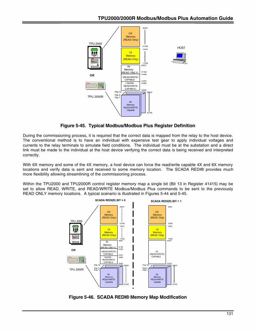
TPU2000/2000R Modbus/Modbus Plus Automation Guide
131
CC EE
TARGETS
EC
TPU 2000
TPU 2000R
OR
OX Memory
(READ Only)
1X Memory
(READ Only)
6X Memory
READ/WRITECapable
00001
01056
10001
11056
File 1File 2File 10 60000
63199
40001
4118241409
4145741665
42945
4x Memory(READ ONLY)
(READ/WRITE) CAPABLE
( QUASI-READ/WRITE CAPABLE)
HOST
Figure 5-45. Typical Modbus/Modbus Plus Register Definition
During the commissioning process, it is required that the correct data is mapped from the relay to the host device.The conventional method is to have an individual with expensive test gear to apply individual voltages andcurrents to the relay terminals to simulate field conditions. The individual must be at the substation and a directlink must be made to the individual at the host device verifying the correct data is being received and interpretedcorrectly.
With 6X memory and some of the 4X memory, a host device can force the read/write capable 4X and 6X memorylocations and verify data is sent and received to some memory location. The SCADA REDI® provides muchmore flexibility allowing streamlining of the commissioning process.
Within the TPU2000 and TPU2000R control register memory map a single bit (Bit 13 in Register 41415) may beset to allow READ, WRITE, and READ/WRITE Modbus/Modbus Plus commands to be sent to the previouslyREAD ONLY memory locations. A typical scenario is illustrated in Figures 5-44 and 5-45.
CC EE
TARGETS
EC
TPU 2000
TPU 2000R
OR
OX Memory
(READ Only)
1X Memory
(READ Only)
6X Memory
READ/WRITECapable
00001
01056
10001
11056
File 1File 2File 10 60000
63199
40001
4118241409
4145741665
42925
4x Memory(READ ONLY)
(READ/WRITE) CAPABLE QUASI-READ/WRITE CAPABLE
SCADA REDI(R) BIT = 0
OX Memory
(READ Only)
1X Memory
(READ Only)
6X Memory
READ/WRITECapable
00001
01056
10001
11056
File 1File 2File 10 60000
63199
40001
42925
4X(READ/WRITE) CAPABLE
SCADA REDI(R) BIT = 1
Figure 5-46. SCADA REDI® Memory Map Modification
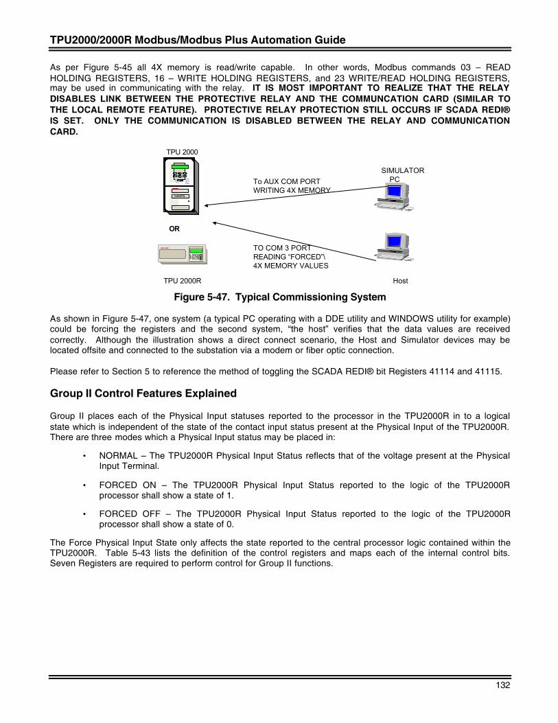
TPU2000/2000R Modbus/Modbus Plus Automation Guide
132
As per Figure 5-45 all 4X memory is read/write capable. In other words, Modbus commands 03 – READHOLDING REGISTERS, 16 – WRITE HOLDING REGISTERS, and 23 WRITE/READ HOLDING REGISTERS,may be used in communicating with the relay. IT IS MOST IMPORTANT TO REALIZE THAT THE RELAYDISABLES LINK BETWEEN THE PROTECTIVE RELAY AND THE COMMUNCATION CARD (SIMILAR TOTHE LOCAL REMOTE FEATURE). PROTECTIVE RELAY PROTECTION STILL OCCURS IF SCADA REDI®IS SET. ONLY THE COMMUNICATION IS DISABLED BETWEEN THE RELAY AND COMMUNICATIONCARD.
CC EE
TARGETS
EC
TPU 2000
TPU 2000R
OR
SIMULATOR PCTo AUX COM PORT
WRITING 4X MEMORY
Host
TO COM 3 PORTREADING “FORCED”\4X MEMORY VALUES
Figure 5-47. Typical Commissioning System
As shown in Figure 5-47, one system (a typical PC operating with a DDE utility and WINDOWS utility for example)could be forcing the registers and the second system, “the host” verifies that the data values are receivedcorrectly. Although the illustration shows a direct connect scenario, the Host and Simulator devices may belocated offsite and connected to the substation via a modem or fiber optic connection.
Please refer to Section 5 to reference the method of toggling the SCADA REDI® bit Registers 41114 and 41115.
Group II Control Features Explained
Group II places each of the Physical Input statuses reported to the processor in the TPU2000R in to a logicalstate which is independent of the state of the contact input status present at the Physical Input of the TPU2000R.There are three modes which a Physical Input status may be placed in:
• NORMAL – The TPU2000R Physical Input Status reflects that of the voltage present at the PhysicalInput Terminal.
• FORCED ON – The TPU2000R Physical Input Status reported to the logic of the TPU2000Rprocessor shall show a state of 1.
• FORCED OFF – The TPU2000R Physical Input Status reported to the logic of the TPU2000Rprocessor shall show a state of 0.
The Force Physical Input State only affects the state reported to the central processor logic contained within theTPU2000R. Table 5-43 lists the definition of the control registers and maps each of the internal control bits.Seven Registers are required to perform control for Group II functions.
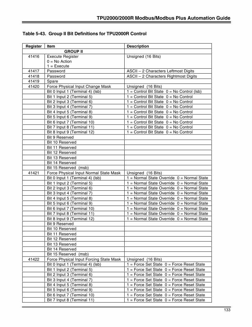
TPU2000/2000R Modbus/Modbus Plus Automation Guide
133
Table 5-43. Group II Bit Definitions for TPU2000R Control
Register Item DescriptionGROUP II
41416 Execute Register0 = No Action1 = Execute
Unsigned (16 Bits)
41417 Password ASCII – 2 Characters Leftmost Digits41418 Password ASCII – 2 Characters Rightmost Digits41419 Spare41420 Force Physical Input Change Mask Unsigned (16 Bits)
Bit 0 Input 1 (Terminal 4) (lsb) 1 = Control Bit State 0 = No Control (lsb)Bit 1 Input 2 (Terminal 5) 1 = Control Bit State 0 = No ControlBit 2 Input 3 (Terminal 6) 1 = Control Bit State 0 = No ControlBit 3 Input 4 (Terminal 7) 1 = Control Bit State 0 = No ControlBit 4 Input 5 (Terminal 8) 1 = Control Bit State 0 = No ControlBit 5 Input 6 (Terminal 9) 1 = Control Bit State 0 = No ControlBit 6 Input 7 (Terminal 10) 1 = Control Bit State 0 = No ControlBit 7 Input 8 (Terminal 11) 1 = Control Bit State 0 = No ControlBit 8 Input 9 (Terminal 12) 1 = Control Bit State 0 = No ControlBit 9 ReservedBit 10 ReservedBit 11 ReservedBit 12 ReservedBit 13 ReservedBit 14 ReservedBit 15 Reserved (msb)
41421 Force Physical Input Normal State Mask Unsigned (16 Bits)Bit 0 Input 1 (Terminal 4) (lsb) 1 = Normal State Override 0 = Normal StateBit 1 Input 2 (Terminal 5) 1 = Normal State Override 0 = Normal StateBit 2 Input 3 (Terminal 6) 1 = Normal State Override 0 = Normal StateBit 3 Input 4 (Terminal 7) 1 = Normal State Override 0 = Normal StateBit 4 Input 5 (Terminal 8) 1 = Normal State Override 0 = Normal StateBit 5 Input 6 (Terminal 9) 1 = Normal State Override 0 = Normal StateBit 6 Input 7 (Terminal 10) 1 = Normal State Override 0 = Normal StateBit 7 Input 8 (Terminal 11) 1 = Normal State Override 0 = Normal StateBit 8 Input 9 (Terminal 12) 1 = Normal State Override 0 = Normal StateBit 9 ReservedBit 10 ReservedBit 11 ReservedBit 12 ReservedBit 13 ReservedBit 14 ReservedBit 15 Reserved (msb)
41422 Force Physical Input Forcing State Mask Unsigned (16 Bits)Bit 0 Input 1 (Terminal 4) (lsb) 1 = Force Set State 0 = Force Reset StateBit 1 Input 2 (Terminal 5) 1 = Force Set State 0 = Force Reset StateBit 2 Input 3 (Terminal 6) 1 = Force Set State 0 = Force Reset StateBit 3 Input 4 (Terminal 7) 1 = Force Set State 0 = Force Reset StateBit 4 Input 5 (Terminal 8) 1 = Force Set State 0 = Force Reset StateBit 5 Input 6 (Terminal 9) 1 = Force Set State 0 = Force Reset StateBit 6 Input 7 (Terminal 10) 1 = Force Set State 0 = Force Reset StateBit 7 Input 8 (Terminal 11) 1 = Force Set State 0 = Force Reset State
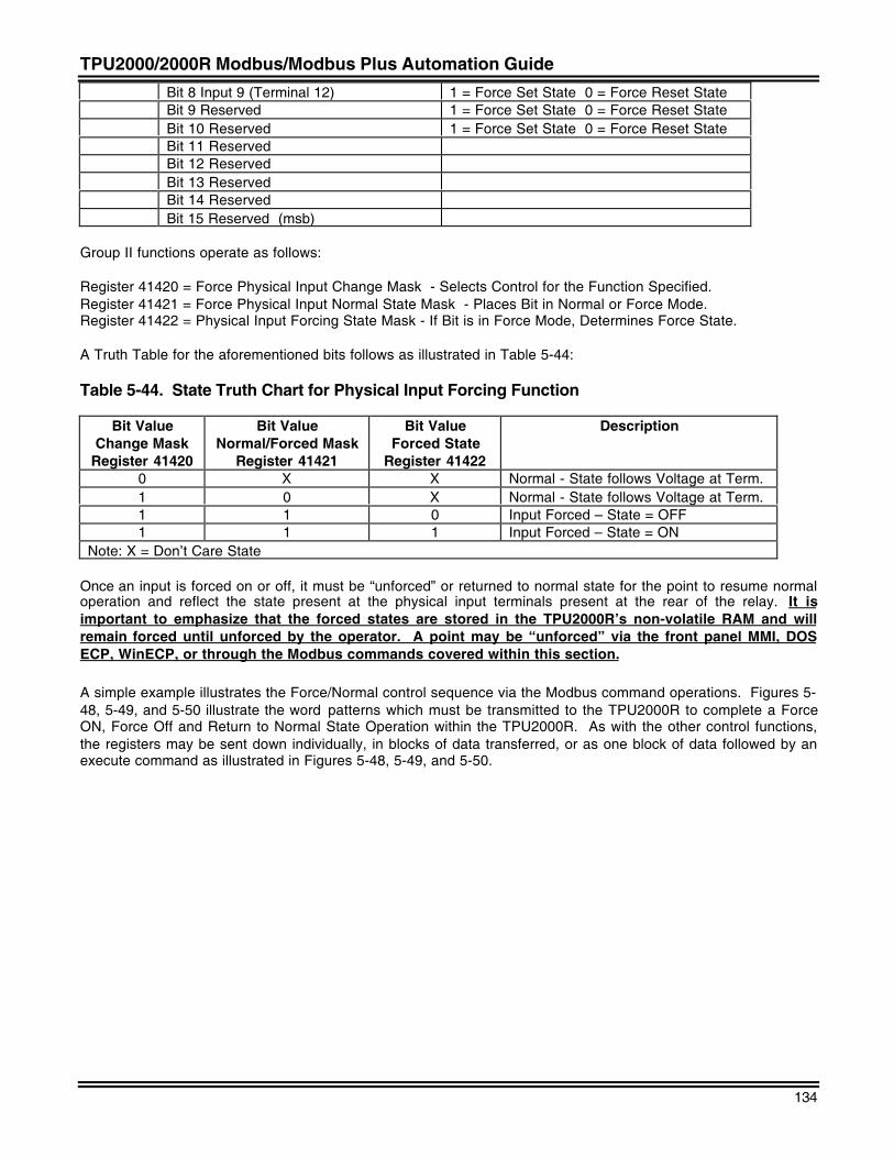
TPU2000/2000R Modbus/Modbus Plus Automation Guide
134
Bit 8 Input 9 (Terminal 12) 1 = Force Set State 0 = Force Reset StateBit 9 Reserved 1 = Force Set State 0 = Force Reset StateBit 10 Reserved 1 = Force Set State 0 = Force Reset StateBit 11 ReservedBit 12 ReservedBit 13 ReservedBit 14 ReservedBit 15 Reserved (msb)
Group II functions operate as follows:
Register 41420 = Force Physical Input Change Mask - Selects Control for the Function Specified.Register 41421 = Force Physical Input Normal State Mask - Places Bit in Normal or Force Mode.Register 41422 = Physical Input Forcing State Mask - If Bit is in Force Mode, Determines Force State.
A Truth Table for the aforementioned bits follows as illustrated in Table 5-44:
Table 5-44. State Truth Chart for Physical Input Forcing Function
Bit ValueChange Mask
Register 41420
Bit ValueNormal/Forced Mask
Register 41421
Bit ValueForced State
Register 41422
Description
0 X X Normal - State follows Voltage at Term.1 0 X Normal - State follows Voltage at Term.1 1 0 Input Forced – State = OFF1 1 1 Input Forced – State = ON
Note: X = Don’t Care State
Once an input is forced on or off, it must be “unforced” or returned to normal state for the point to resume normaloperation and reflect the state present at the physical input terminals present at the rear of the relay. It isimportant to emphasize that the forced states are stored in the TPU2000R’s non-volatile RAM and willremain forced until unforced by the operator. A point may be “unforced” via the front panel MMI, DOSECP, WinECP, or through the Modbus commands covered within this section.
A simple example illustrates the Force/Normal control sequence via the Modbus command operations. Figures 5-48, 5-49, and 5-50 illustrate the word patterns which must be transmitted to the TPU2000R to complete a ForceON, Force Off and Return to Normal State Operation within the TPU2000R. As with the other control functions,the registers may be sent down individually, in blocks of data transferred, or as one block of data followed by anexecute command as illustrated in Figures 5-48, 5-49, and 5-50.
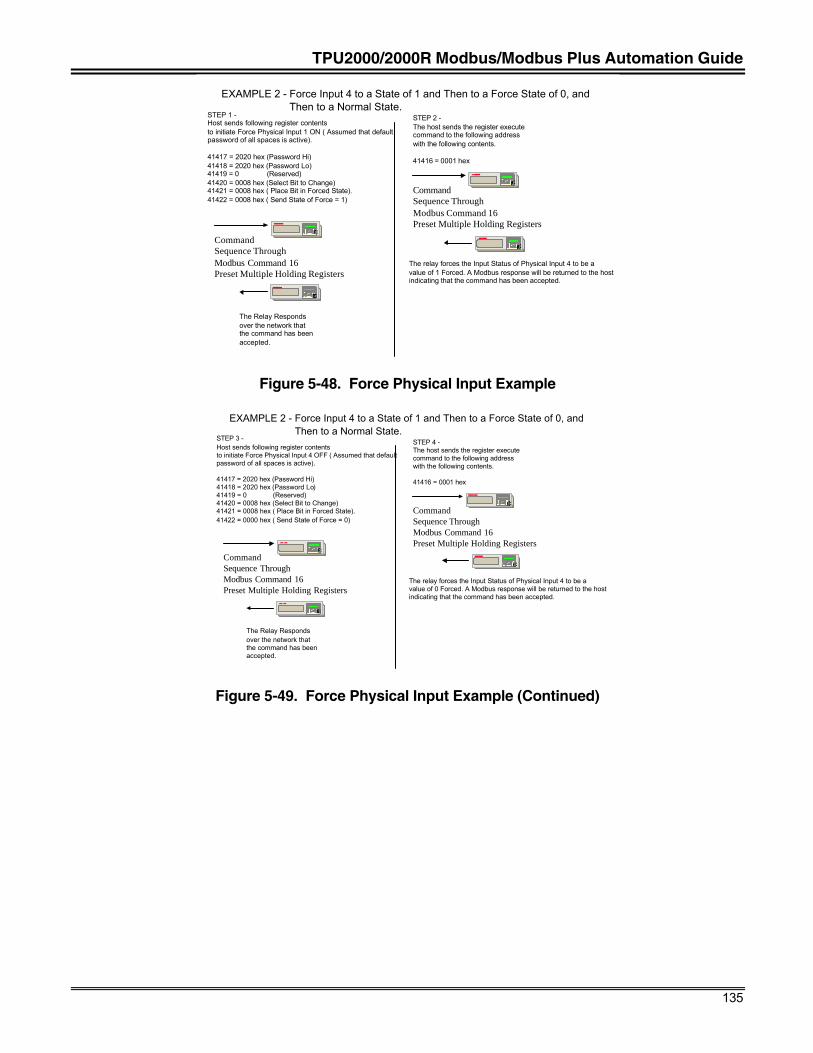
TPU2000/2000R Modbus/Modbus Plus Automation Guide
135
EC
CommandSequence ThroughModbus Command 16Preset Multiple Holding Registers
STEP 1 -Host sends following register contentsto initiate Force Physical Input 1 ON ( Assumed that defaultpassword of all spaces is active).
41417 = 2020 hex (Password Hi)41418 = 2020 hex (Password Lo)41419 = 0 (Reserved)41420 = 0008 hex (Select Bit to Change)41421 = 0008 hex ( Place Bit in Forced State).41422 = 0008 hex ( Send State of Force = 1)
EXAMPLE 2 - Force Input 4 to a State of 1 and Then to a Force State of 0, and Then to a Normal State.
EC
The relay forces the Input Status of Physical Input 4 to be a value of 1 Forced. A Modbus response will be returned to the hostindicating that the command has been accepted.
EC
CommandSequence ThroughModbus Command 16Preset Multiple Holding Registers
STEP 2 -The host sends the register executecommand to the following address with the following contents.
41416 = 0001 hex
EC
The Relay Respondsover the network that the command has been accepted.
Figure 5-48. Force Physical Input Example
EC
CommandSequence ThroughModbus Command 16Preset Multiple Holding Registers
STEP 3 -Host sends following register contentsto initiate Force Physical Input 4 OFF ( Assumed that defaultpassword of all spaces is active).
41417 = 2020 hex (Password Hi)41418 = 2020 hex (Password Lo)41419 = 0 (Reserved)41420 = 0008 hex (Select Bit to Change)41421 = 0008 hex ( Place Bit in Forced State).41422 = 0000 hex ( Send State of Force = 0)
EXAMPLE 2 - Force Input 4 to a State of 1 and Then to a Force State of 0, and Then to a Normal State.
EC
The relay forces the Input Status of Physical Input 4 to be a value of 0 Forced. A Modbus response will be returned to the hostindicating that the command has been accepted.
EC
CommandSequence ThroughModbus Command 16Preset Multiple Holding Registers
STEP 4 -The host sends the register executecommand to the following address with the following contents.
41416 = 0001 hex
EC
The Relay Respondsover the network that the command has been accepted.
Figure 5-49. Force Physical Input Example (Continued)
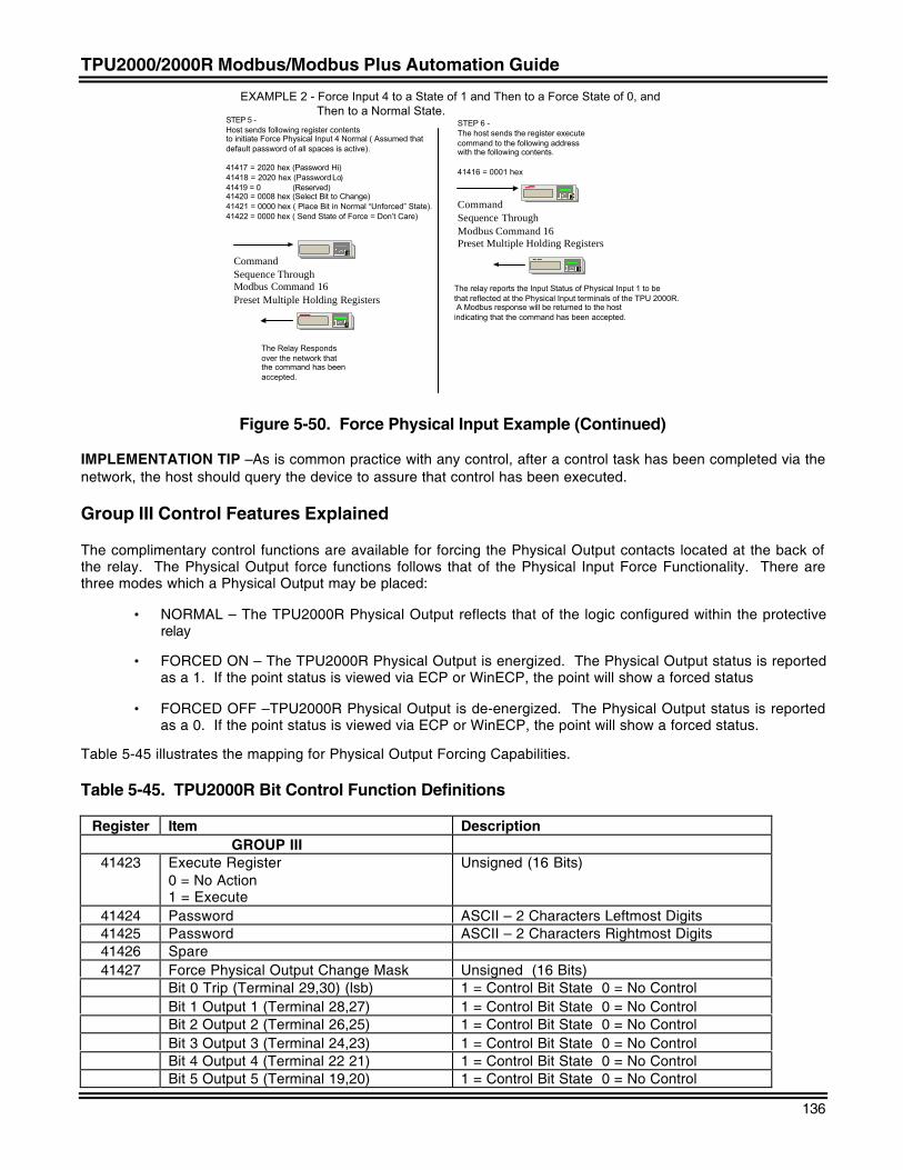
TPU2000/2000R Modbus/Modbus Plus Automation Guide
136
EC
CommandSequence ThroughModbus Command 16Preset Multiple Holding Registers
STEP 5 -Host sends following register contentsto initiate Force Physical Input 4 Normal ( Assumed that default password of all spaces is active).
41417 = 2020 hex (Password Hi)41418 = 2020 hex (Password Lo)41419 = 0 (Reserved)41420 = 0008 hex (Select Bit to Change)41421 = 0000 hex ( Place Bit in Normal “Unforced” State).41422 = 0000 hex ( Send State of Force = Don’t Care)
EXAMPLE 2 - Force Input 4 to a State of 1 and Then to a Force State of 0, and Then to a Normal State.
EC
The relay reports the Input Status of Physical Input 1 to be that reflected at the Physical Input terminals of the TPU 2000R. A Modbus response will be returned to the hostindicating that the command has been accepted.
EC
CommandSequence ThroughModbus Command 16Preset Multiple Holding Registers
STEP 6 -The host sends the register executecommand to the following address with the following contents.
41416 = 0001 hex
EC
The Relay Respondsover the network that the command has been accepted.
Figure 5-50. Force Physical Input Example (Continued)
IMPLEMENTATION TIP –As is common practice with any control, after a control task has been completed via thenetwork, the host should query the device to assure that control has been executed.
Group III Control Features Explained
The complimentary control functions are available for forcing the Physical Output contacts located at the back ofthe relay. The Physical Output force functions follows that of the Physical Input Force Functionality. There arethree modes which a Physical Output may be placed:
• NORMAL – The TPU2000R Physical Output reflects that of the logic configured within the protectiverelay
• FORCED ON – The TPU2000R Physical Output is energized. The Physical Output status is reportedas a 1. If the point status is viewed via ECP or WinECP, the point will show a forced status
• FORCED OFF –TPU2000R Physical Output is de-energized. The Physical Output status is reportedas a 0. If the point status is viewed via ECP or WinECP, the point will show a forced status.
Table 5-45 illustrates the mapping for Physical Output Forcing Capabilities.
Table 5-45. TPU2000R Bit Control Function Definitions
Register Item DescriptionGROUP III
41423 Execute Register0 = No Action1 = Execute
Unsigned (16 Bits)
41424 Password ASCII – 2 Characters Leftmost Digits41425 Password ASCII – 2 Characters Rightmost Digits41426 Spare41427 Force Physical Output Change Mask Unsigned (16 Bits)
Bit 0 Trip (Terminal 29,30) (lsb) 1 = Control Bit State 0 = No ControlBit 1 Output 1 (Terminal 28,27) 1 = Control Bit State 0 = No ControlBit 2 Output 2 (Terminal 26,25) 1 = Control Bit State 0 = No ControlBit 3 Output 3 (Terminal 24,23) 1 = Control Bit State 0 = No ControlBit 4 Output 4 (Terminal 22 21) 1 = Control Bit State 0 = No ControlBit 5 Output 5 (Terminal 19,20) 1 = Control Bit State 0 = No Control
TPU2000/2000R Modbus/Modbus Plus Automation Guide
137
Bit 6 Output 6 (Terminal 17,18) 1 = Control Bit State 0 = No ControlBit 7 Output 7 1 = Control Bit State 0 = No ControlBit 8 ReservedBit 9 ReservedBit 10 ReservedBit 11 ReservedBit 12 ReservedBit 13 ReservedBit 14 Reserved
41428 Force Physical Output Normal State Mask Unsigned (16 Bits)Bit 0 Trip (Terminal 29,30) (lsb) 1 = Normal State Override 0 = Normal StateBit 1 Output 1 (Terminal 28,27) 1 = Normal State Override 0 = Normal StateBit 2 Output 2 (Terminal 26,25) 1 = Normal State Override 0 = Normal StateBit 3 Output 3 (Terminal 24,23) 1 = Normal State Override 0 = Normal StateBit 4 Output 4 (Terminal 22 21) 1 = Normal State Override 0 = Normal StateBit 5 Output 5 (Terminal 19,20) 1 = Normal State Override 0 = Normal StateBit 6 Output 6 (Terminal 17,18) 1 = Normal State Override 0 = Normal StateBit 7 Output 7 1 = Normal State Override 0 = Normal StateBit 8 ReservedBit 9 ReservedBit 10 ReservedBit 11 ReservedBit 12 ReservedBit 13 ReservedBit 14 ReservedBit 15 Reserved (msb)
41429 Force Physical Input Forcing State Mask Unsigned (16 Bits)Bit 0 Trip (Terminal 29,30) (lsb) 1 = Force Set State 0 = Force Reset StateBit 1 Output 1 (Terminal 28,27) 1 = Force Set State 0 = Force Reset StateBit 2 Output 2 (Terminal 26,25) 1 = Force Set State 0 = Force Reset StateBit 3 Output 3 (Terminal 24,23) 1 = Force Set State 0 = Force Reset StateBit 4 Output 4 (Terminal 22 21) 1 = Force Set State 0 = Force Reset StateBit 5 Output 5 (Terminal 19,20) 1 = Force Set State 0 = Force Reset StateBit 6 Output 6 (Terminal 17,18) 1 = Force Set State 0 = Force Reset StateBit 7 Output 7 1 = Force Set State 0 = Force Reset StateBit 8 ReservedBit 9 ReservedBit 10 ReservedBit 11 ReservedBit 12 ReservedBit 13 ReservedBit 14 ReservedBit 15 Reserved (msb)
Group III functions operate as follows:
Register 41427 = Force Physical Output Change Mask - Selects Control for the Function SpecifiedRegister 41428 = Force Physical Output Normal State Mask - Places Bit in Normal or Force Mode.Register 41429 = Physical Output Forcing State Mask – If Bit is in Force Mode, Determines Force State (State 1= energized State 0 = de-energized).
A Truth Table for the aforementioned bits follows as illustrated in Table 5-46:
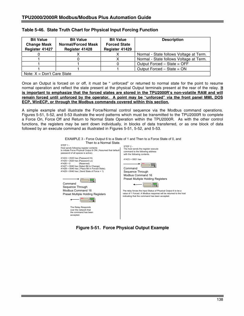
TPU2000/2000R Modbus/Modbus Plus Automation Guide
138
Table 5-46. State Truth Chart for Physical Input Forcing Function
Bit ValueChange Mask
Register 41427
Bit ValueNormal/Forced Mask
Register 41428
Bit ValueForced State
Register 41429
Description
0 X X Normal - State follows Voltage at Term.1 0 X Normal - State follows Voltage at Term.1 1 0 Output Forced – State = OFF1 1 1 Output Forced – State = ON
Note: X = Don’t Care State
Once an Output is forced on or off, it must be “ unforced” or returned to normal state for the point to resumenormal operation and reflect the state present at the physical Output terminals present at the rear of the relay. Itis important to emphasize that the forced states are stored in the TPU2000R’s non-volatile RAM and willremain forced until unforced by the operator. A point may be “unforced” via the front panel MMI, DOSECP, WinECP, or through the Modbus commands covered within this section.
A simple example shall illustrate the Force/Normal control sequence via the Modbus command operations.Figures 5-51, 5-52, and 5-53 illustrate the word patterns which must be transmitted to the TPU2000R to completea Force On, Force Off and Return to Normal State Operation within the TPU2000R. As with the other controlfunctions, the registers may be sent down individually, in blocks of data transferred, or as one block of datafollowed by an execute command as illustrated in Figures 5-51, 5-52, and 5-53.
EC
CommandSequence ThroughModbus Command 16Preset Multiple Holding Registers
STEP 1 -Host sends following register contentsto initiate Force Physical Output 6 ON ( Assumed that defaultpassword of all spaces is active).
41424 = 2020 hex (Password Hi)41425 = 2020 hex (Password Lo)41426 = 0 (Reserved)41427 = 0040 hex (Select Bit to Change)41428 = 0040 hex ( Place Bit in Forced State).41429 = 0040 hex ( Send State of Force = 1)
EXAMPLE 3 - Force Output 6 to a State of 1 and Then to a Force State of 0, and Then to a Normal State.
EC
The relay forces the Input Status of Physical Output 6 to be a value of 1 Forced. A Modbus response will be returned to the hostindicating that the command has been accepted.
EC
CommandSequence ThroughModbus Command 16Preset Multiple Holding Registers
STEP 2 -The host sends the register executecommand to the following address with the following contents.
41423 = 0001 hex
EC
The Relay Respondsover the network that the command has been accepted.
Figure 5-51. Force Physical Output Example
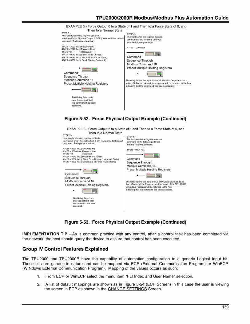
TPU2000/2000R Modbus/Modbus Plus Automation Guide
139
EC
CommandSequence ThroughModbus Command 16Preset Multiple Holding Registers
STEP 3 -Host sends following register contentsto initiate Force Physical Output 6 OFF ( Assumed that defaultpassword of all spaces is active).
41424 = 2020 hex (Password Hi)41425 = 2020 hex (Password Lo)41426 = 0 (Reserved)41427 = 0040 hex (Select Bit to Change)41428 = 0040 hex ( Place Bit in Forced State).41429 = 0000 hex ( Send State of Force = 0)
EXAMPLE 3 - Force Output 6 to a State of 1 and Then to a Force State of 0, and Then to a Normal State.
EC
The relay forces the Input Status of Physical Output 6 to be a value of 0 Forced. A Modbus response will be returned to the hostindicating that the command has been accepted.
EC
CommandSequence ThroughModbus Command 16Preset Multiple Holding Registers
STEP 4 -The host sends the register executecommand to the following address with the following contents.
41423 = 0001 hex
EC
The Relay Respondsover the network that the command has been accepted.
Figure 5-52. Force Physical Output Example (Continued)
ECCommandSequence ThroughModbus Command 16Preset Multiple Holding Registers
STEP 5 -Host sends following register contentsto initiate Force Physical Output 8 ON ( Assumed that defaultpassword of all spaces is active).
41424 = 2020 hex (Password Hi)41425 = 2020 hex (Password Lo)41426 = 0 (Reserved)41427 = 0040 hex (Select Bit to Change)41428 = 0000 hex ( Place Bit in Normal “Unforced” State).41429 = 0000 hex ( Send State of Force = Don’t Care)
EXAMPLE 3 - Force Output 6 to a State of 1 and Then to a Force State of 0, and Then to a Normal State.
EC
The relay reports the Input Status of Physical Output 6 to be that reflected at the Physical Input terminals of the TPU 2000R. A Modbus response will be returned to the hostindicating that the command has been accepted.
EC
CommandSequence ThroughModbus Command 16Preset Multiple Holding Registers
STEP 6 -The host sends the register executecommand to the following address with the following contents.
41423 = 0001 hex
EC
The Relay Respondsover the network that the command has been accepted.
Figure 5-53. Force Physical Output Example (Continued)
IMPLEMENTATION TIP – As is common practice with any control, after a control task has been completed viathe network, the host should query the device to assure that control has been executed.
Group IV Control Features Explained
The TPU2000 and TPU2000R have the capability of automation configuration to a generic Logical Input bit.These bits are generic in nature and can be mapped via ECP (External Communication Program) or WinECP(WINdows External Communication Program). Mapping of the values occurs as such:
1. From ECP or WinECP select the menu item “FLI Index and User Name” selection.
2. A list of default mappings are shown as in Figure 5-54 (ECP Screen) In this case the user is viewingthe screen in ECP as shown in the CHANGE SETTINGS Screen.
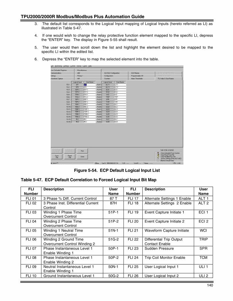
TPU2000/2000R Modbus/Modbus Plus Automation Guide
140
3. The default list corresponds to the Logical Input mapping of Logical Inputs (hereto referred as LI) asillustrated in Table 5-47.
4. If one would wish to change the relay protective function element mapped to the specific LI, depressthe “ENTER” key. The display in Figure 5-55 shall result.
5. The user would then scroll down the list and highlight the element desired to be mapped to thespecific LI within the edited list.
6. Depress the “ENTER” key to map the selected element into the table.
Figure 5-54. ECP Default Logical Input List
Table 5-47. ECP Default Correlation to Forced Logical Input Bit Map
FLINumber
Description UserName
FLINumber
Description UserName
FLI 01 3 Phase % Diff. Current Control 87 T FLI 17 Alternate Settings 1 Enable ALT 1FLI 02 3 Phase Inst. Differential Current
Control87H FLI 18 Alternate Settings 2 Enable ALT 2
FLI 03 Winding 1 Phase TimeOvercurrent Control
51P-1 FLI 19 Event Capture Initiate 1 ECI 1
FLI 04 Winding 2 Phase TimeOvercurrent Control
51P-2 FLI 20 Event Capture Initiate 2 ECI 2
FLI 05 Winding 1 Neutral TimeOvercurrent Control
51N-1 FLI 21 Waveform Capture Initiate WCI
FLI 06 Winding 2 Ground TimeOvercurrent Control Winding 2
51G-2 FLI 22 Differential Trip OutputContact Enable
TRIP
FLI 07 Phase Instantaneous Level 1Enable Winding 1
50P-1 FLI 23 Sudden Pressure SPR
FLI 08 Phase Instantaneous Level 1Enable Winding 2
50P-2 FLI 24 Trip Coil Monitor Enable TCM
FLI 09 Neutral Instantaneous Level 1Enable Winding 1
50N-1 FLI 25 User Logical Input 1 ULI 1
FLI 10 Ground Instantaneous Level 1 50G-2 FLI 26 User Logical Input 2 ULI 2
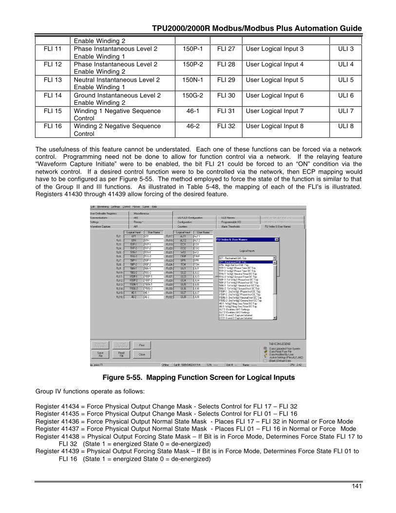
TPU2000/2000R Modbus/Modbus Plus Automation Guide
141
Enable Winding 2FLI 11 Phase Instantaneous Level 2
Enable Winding 1150P-1 FLI 27 User Logical Input 3 ULI 3
FLI 12 Phase Instantaneous Level 2Enable Winding 2
150P-2 FLI 28 User Logical Input 4 ULI 4
FLI 13 Neutral Instantaneous Level 2Enable Winding 1
150N-1 FLI 29 User Logical Input 5 ULI 5
FLI 14 Ground Instantaneous Level 2Enable Winding 2
150G-2 FLI 30 User Logical Input 6 ULI 6
FLI 15 Winding 1 Negative SequenceControl
46-1 FLI 31 User Logical Input 7 ULI 7
FLI 16 Winding 2 Negative SequenceControl
46-2 FLI 32 User Logical Input 8 ULI 8
The usefulness of this feature cannot be understated. Each one of these functions can be forced via a networkcontrol. Programming need not be done to allow for function control via a network. If the relaying feature“Waveform Capture Initiate” were to be enabled, the bit FLI 21 could be forced to an “ON” condition via thenetwork control. If a desired control function were to be controlled via the network, then ECP mapping wouldhave to be configured as per Figure 5-55. The method employed to force the state of the function is similar to thatof the Group II and III functions. As illustrated in Table 5-48, the mapping of each of the FLI’s is illustrated.Registers 41430 through 41439 allow forcing of the desired feature.
Figure 5-55. Mapping Function Screen for Logical Inputs
Group IV functions operate as follows:
Register 41434 = Force Physical Output Change Mask - Selects Control for FLI 17 – FLI 32Register 41435 = Force Physical Output Change Mask - Selects Control for FLI 01 – FLI 16Register 41436 = Force Physical Output Normal State Mask - Places FLI 17 – FLI 32 in Normal or Force ModeRegister 41437 = Force Physical Output Normal State Mask - Places FLI 01 – FLI 16 in Normal or Force ModeRegister 41438 = Physical Output Forcing State Mask – If Bit is in Force Mode, Determines Force State FLI 17 to
FLI 32 (State 1 = energized State 0 = de-energized)Register 41439 = Physical Output Forcing State Mask – If Bit is in Force Mode, Determines Force State FLI 01 to
FLI 16 (State 1 = energized State 0 = de-energized)
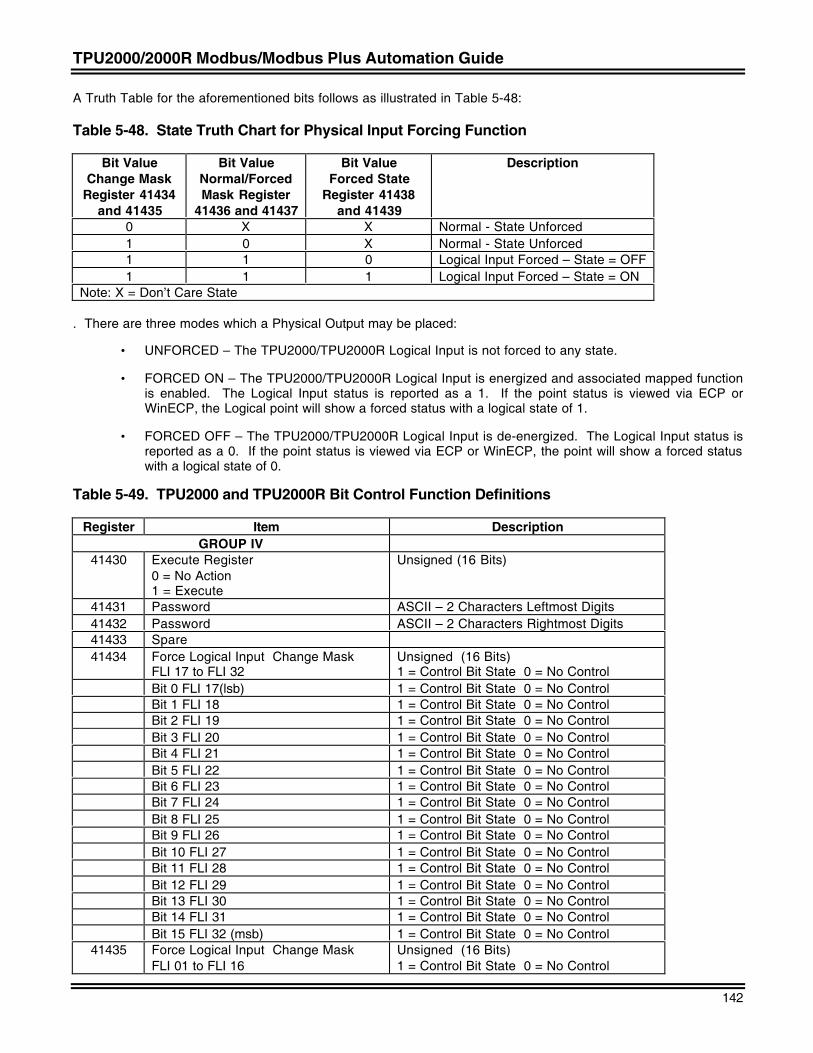
TPU2000/2000R Modbus/Modbus Plus Automation Guide
142
A Truth Table for the aforementioned bits follows as illustrated in Table 5-48:
Table 5-48. State Truth Chart for Physical Input Forcing Function
Bit ValueChange Mask
Register 41434and 41435
Bit ValueNormal/ForcedMask Register
41436 and 41437
Bit ValueForced State
Register 41438and 41439
Description
0 X X Normal - State Unforced1 0 X Normal - State Unforced1 1 0 Logical Input Forced – State = OFF1 1 1 Logical Input Forced – State = ON
Note: X = Don’t Care State
. There are three modes which a Physical Output may be placed:
• UNFORCED – The TPU2000/TPU2000R Logical Input is not forced to any state.
• FORCED ON – The TPU2000/TPU2000R Logical Input is energized and associated mapped functionis enabled. The Logical Input status is reported as a 1. If the point status is viewed via ECP orWinECP, the Logical point will show a forced status with a logical state of 1.
• FORCED OFF – The TPU2000/TPU2000R Logical Input is de-energized. The Logical Input status isreported as a 0. If the point status is viewed via ECP or WinECP, the point will show a forced statuswith a logical state of 0.
Table 5-49. TPU2000 and TPU2000R Bit Control Function Definitions
Register Item DescriptionGROUP IV
41430 Execute Register0 = No Action1 = Execute
Unsigned (16 Bits)
41431 Password ASCII – 2 Characters Leftmost Digits41432 Password ASCII – 2 Characters Rightmost Digits41433 Spare41434 Force Logical Input Change Mask
FLI 17 to FLI 32Unsigned (16 Bits)1 = Control Bit State 0 = No Control
Bit 0 FLI 17(lsb) 1 = Control Bit State 0 = No ControlBit 1 FLI 18 1 = Control Bit State 0 = No ControlBit 2 FLI 19 1 = Control Bit State 0 = No ControlBit 3 FLI 20 1 = Control Bit State 0 = No ControlBit 4 FLI 21 1 = Control Bit State 0 = No ControlBit 5 FLI 22 1 = Control Bit State 0 = No ControlBit 6 FLI 23 1 = Control Bit State 0 = No ControlBit 7 FLI 24 1 = Control Bit State 0 = No ControlBit 8 FLI 25 1 = Control Bit State 0 = No ControlBit 9 FLI 26 1 = Control Bit State 0 = No ControlBit 10 FLI 27 1 = Control Bit State 0 = No ControlBit 11 FLI 28 1 = Control Bit State 0 = No ControlBit 12 FLI 29 1 = Control Bit State 0 = No ControlBit 13 FLI 30 1 = Control Bit State 0 = No ControlBit 14 FLI 31 1 = Control Bit State 0 = No ControlBit 15 FLI 32 (msb) 1 = Control Bit State 0 = No Control
41435 Force Logical Input Change MaskFLI 01 to FLI 16
Unsigned (16 Bits)1 = Control Bit State 0 = No Control
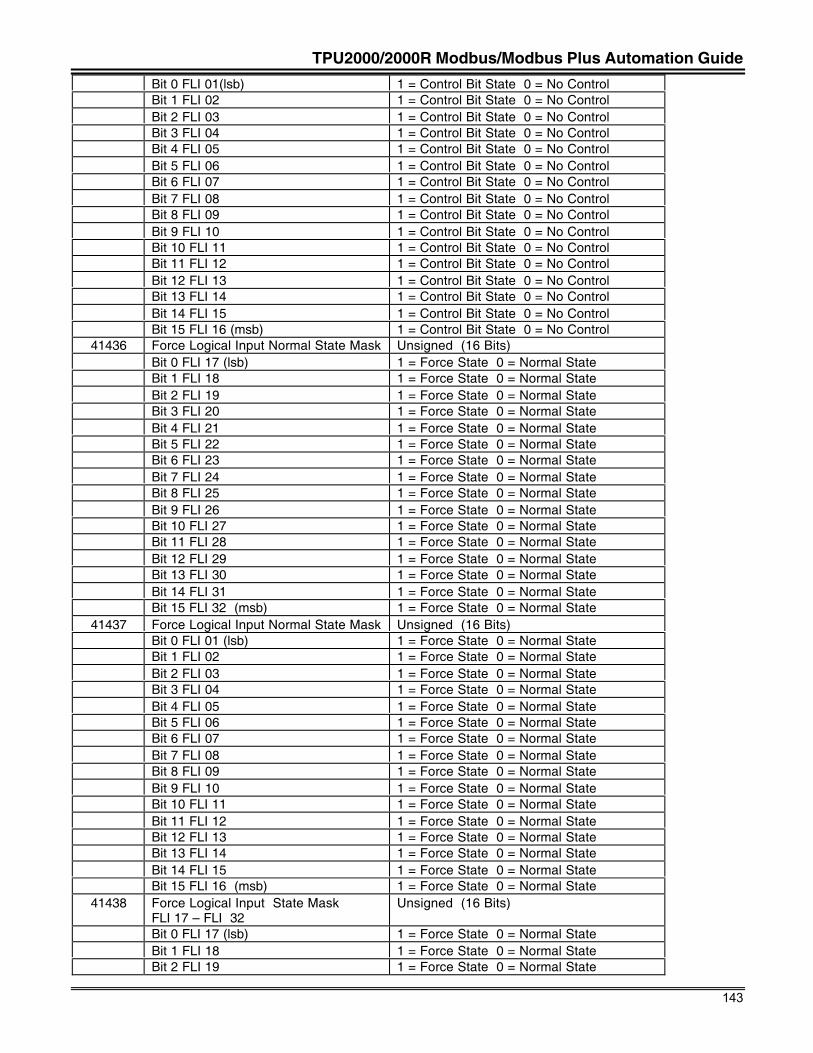
TPU2000/2000R Modbus/Modbus Plus Automation Guide
143
Bit 0 FLI 01(lsb) 1 = Control Bit State 0 = No ControlBit 1 FLI 02 1 = Control Bit State 0 = No ControlBit 2 FLI 03 1 = Control Bit State 0 = No ControlBit 3 FLI 04 1 = Control Bit State 0 = No ControlBit 4 FLI 05 1 = Control Bit State 0 = No ControlBit 5 FLI 06 1 = Control Bit State 0 = No ControlBit 6 FLI 07 1 = Control Bit State 0 = No ControlBit 7 FLI 08 1 = Control Bit State 0 = No ControlBit 8 FLI 09 1 = Control Bit State 0 = No ControlBit 9 FLI 10 1 = Control Bit State 0 = No ControlBit 10 FLI 11 1 = Control Bit State 0 = No ControlBit 11 FLI 12 1 = Control Bit State 0 = No ControlBit 12 FLI 13 1 = Control Bit State 0 = No ControlBit 13 FLI 14 1 = Control Bit State 0 = No ControlBit 14 FLI 15 1 = Control Bit State 0 = No ControlBit 15 FLI 16 (msb) 1 = Control Bit State 0 = No Control
41436 Force Logical Input Normal State Mask Unsigned (16 Bits)Bit 0 FLI 17 (lsb) 1 = Force State 0 = Normal StateBit 1 FLI 18 1 = Force State 0 = Normal StateBit 2 FLI 19 1 = Force State 0 = Normal StateBit 3 FLI 20 1 = Force State 0 = Normal StateBit 4 FLI 21 1 = Force State 0 = Normal StateBit 5 FLI 22 1 = Force State 0 = Normal StateBit 6 FLI 23 1 = Force State 0 = Normal StateBit 7 FLI 24 1 = Force State 0 = Normal StateBit 8 FLI 25 1 = Force State 0 = Normal StateBit 9 FLI 26 1 = Force State 0 = Normal StateBit 10 FLI 27 1 = Force State 0 = Normal StateBit 11 FLI 28 1 = Force State 0 = Normal StateBit 12 FLI 29 1 = Force State 0 = Normal StateBit 13 FLI 30 1 = Force State 0 = Normal StateBit 14 FLI 31 1 = Force State 0 = Normal StateBit 15 FLI 32 (msb) 1 = Force State 0 = Normal State
41437 Force Logical Input Normal State Mask Unsigned (16 Bits)Bit 0 FLI 01 (lsb) 1 = Force State 0 = Normal StateBit 1 FLI 02 1 = Force State 0 = Normal StateBit 2 FLI 03 1 = Force State 0 = Normal StateBit 3 FLI 04 1 = Force State 0 = Normal StateBit 4 FLI 05 1 = Force State 0 = Normal StateBit 5 FLI 06 1 = Force State 0 = Normal StateBit 6 FLI 07 1 = Force State 0 = Normal StateBit 7 FLI 08 1 = Force State 0 = Normal StateBit 8 FLI 09 1 = Force State 0 = Normal StateBit 9 FLI 10 1 = Force State 0 = Normal StateBit 10 FLI 11 1 = Force State 0 = Normal StateBit 11 FLI 12 1 = Force State 0 = Normal StateBit 12 FLI 13 1 = Force State 0 = Normal StateBit 13 FLI 14 1 = Force State 0 = Normal StateBit 14 FLI 15 1 = Force State 0 = Normal StateBit 15 FLI 16 (msb) 1 = Force State 0 = Normal State
41438 Force Logical Input State MaskFLI 17 – FLI 32
Unsigned (16 Bits)
Bit 0 FLI 17 (lsb) 1 = Force State 0 = Normal StateBit 1 FLI 18 1 = Force State 0 = Normal StateBit 2 FLI 19 1 = Force State 0 = Normal State
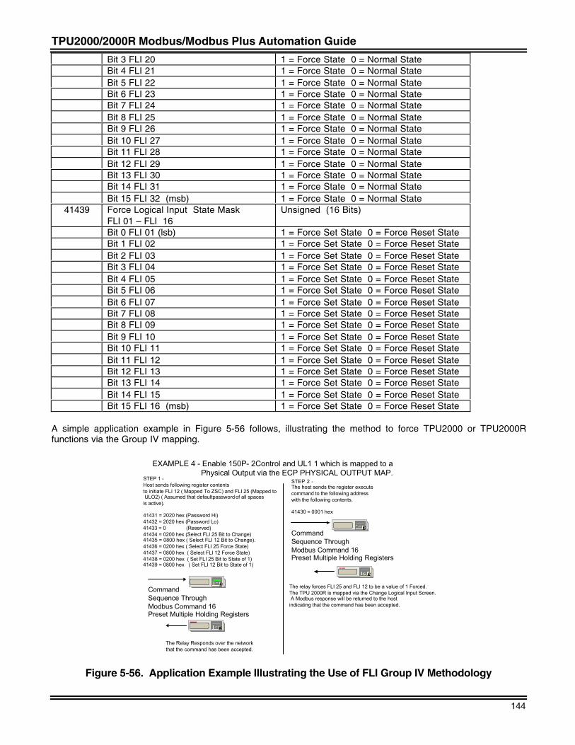
TPU2000/2000R Modbus/Modbus Plus Automation Guide
144
Bit 3 FLI 20 1 = Force State 0 = Normal StateBit 4 FLI 21 1 = Force State 0 = Normal StateBit 5 FLI 22 1 = Force State 0 = Normal StateBit 6 FLI 23 1 = Force State 0 = Normal StateBit 7 FLI 24 1 = Force State 0 = Normal StateBit 8 FLI 25 1 = Force State 0 = Normal StateBit 9 FLI 26 1 = Force State 0 = Normal StateBit 10 FLI 27 1 = Force State 0 = Normal StateBit 11 FLI 28 1 = Force State 0 = Normal StateBit 12 FLI 29 1 = Force State 0 = Normal StateBit 13 FLI 30 1 = Force State 0 = Normal StateBit 14 FLI 31 1 = Force State 0 = Normal StateBit 15 FLI 32 (msb) 1 = Force State 0 = Normal State
41439 Force Logical Input State MaskFLI 01 – FLI 16
Unsigned (16 Bits)
Bit 0 FLI 01 (lsb) 1 = Force Set State 0 = Force Reset StateBit 1 FLI 02 1 = Force Set State 0 = Force Reset StateBit 2 FLI 03 1 = Force Set State 0 = Force Reset StateBit 3 FLI 04 1 = Force Set State 0 = Force Reset StateBit 4 FLI 05 1 = Force Set State 0 = Force Reset StateBit 5 FLI 06 1 = Force Set State 0 = Force Reset StateBit 6 FLI 07 1 = Force Set State 0 = Force Reset StateBit 7 FLI 08 1 = Force Set State 0 = Force Reset StateBit 8 FLI 09 1 = Force Set State 0 = Force Reset StateBit 9 FLI 10 1 = Force Set State 0 = Force Reset StateBit 10 FLI 11 1 = Force Set State 0 = Force Reset StateBit 11 FLI 12 1 = Force Set State 0 = Force Reset StateBit 12 FLI 13 1 = Force Set State 0 = Force Reset StateBit 13 FLI 14 1 = Force Set State 0 = Force Reset StateBit 14 FLI 15 1 = Force Set State 0 = Force Reset StateBit 15 FLI 16 (msb) 1 = Force Set State 0 = Force Reset State
A simple application example in Figure 5-56 follows, illustrating the method to force TPU2000 or TPU2000Rfunctions via the Group IV mapping.
EC
CommandSequence ThroughModbus Command 16Preset Multiple Holding Registers
STEP 1 -Host sends following register contentsto initiate FLI 12 ( Mapped To ZSC) and FLI 25 (Mapped to ULO2) ( Assumed that defaultpassword of all spaces is active).
41431 = 2020 hex (Password Hi)41432 = 2020 hex (Password Lo)41433 = 0 (Reserved)41434 = 0200 hex (Select FLI 25 Bit to Change)41435 = 0800 hex ( Select FLI 12 Bit to Change).41436 = 0200 hex ( Select FLI 25 Force State)41437 = 0800 hex ( Select FLI 12 Force State)41438 = 0200 hex ( Set FLI 25 Bit to State of 1)41439 = 0800 hex ( Set FLI 12 Bit to State of 1)
EXAMPLE 4 - Enable 150P- 2Control and UL1 1 which is mapped to a Physical Output via the ECP PHYSICAL OUTPUT MAP.
EC
The relay forces FLI 25 and FLI 12 to be a value of 1 Forced.The TPU 2000R is mapped via the Change Logical Input Screen. A Modbus response will be returned to the hostindicating that the command has been accepted.
EC
CommandSequence ThroughModbus Command 16Preset Multiple Holding Registers
STEP 2 -The host sends the register executecommand to the following address with the following contents.
41430 = 0001 hex
EC
The Relay Responds over the network that the command has been accepted.
Figure 5-56. Application Example Illustrating the Use of FLI Group IV Methodology
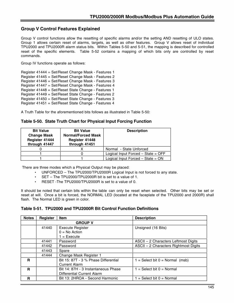
TPU2000/2000R Modbus/Modbus Plus Automation Guide
145
Group V Control Features Explained
Group V control functions allow the resetting of specific alarms and/or the setting AND resetting of ULO states.Group 1 allows certain reset of alarms, targets, as well as other features. Group V allows reset of individualTPU2000 and TPU2000R alarm status bits. Within Tables 5-50 and 5-51, the mapping is described for controlledreset of the specific elements. Table 5-52 contains a mapping of which bits only are controlled by resetcommands.
Group IV functions operate as follows:
Register 41444 = Set/Reset Change Mask - Features 1Register 41445 = Set/Reset Change Mask - Features 2Register 41446 = Set/Reset Change Mask - Features 3Register 41447 = Set/Reset Change Mask - Features 4Register 41448 = Set/Reset State Change - Features 1Register 41449 = Set/Reset State Change - Features 2Register 41450 = Set/Reset State Change - Features 3Register 41451 = Set/Reset State Change - Features 4
A Truth Table for the aforementioned bits follows as illustrated in Table 5-50:
Table 5-50. State Truth Chart for Physical Input Forcing Function
Bit ValueChange Mask
Register 41444through 41447
Bit ValueNormal/Forced Mask
Register 41448through 41451
Description
0 X Normal - State Unforced1 0 Logical Input Forced – State = OFF1 1 Logical Input Forced – State = ON
There are three modes which a Physical Output may be placed:• UNFORCED – The TPU2000/TPU2000R Logical Input is not forced to any state.• SET – The TPU2000/TPU2000R bit is set to a value of 1.• RESET -The TPU2000/TPU2000R is set to a value of 0.
It should be noted that certain bits within the table can only be reset when selected. Other bits may be set orreset at will. Once a bit is forced, the NORMAL LED (located at the faceplate of the TPU2000 and 2000R) shallflash. The Normal LED is green in color.
Table 5-51. TPU2000 and TPU2000R Bit Control Function Definitions
Notes Register Item DescriptionGROUP V
41440 Execute Register0 = No Action1 = Execute
Unsigned (16 Bits)
41441 Password ASCII – 2 Characters Leftmost Digits41442 Password ASCII – 2 Characters Rightmost Digits41443 Spare41444 Change Mask Register 1
R Bit 15: 87T - 3 % Phase DifferentialCurrent Alarm
1 = Select bit 0 = Normal (msb)
R Bit 14: 87H - 3 Instantaneous PhaseDifferential Current Alarm
1 = Select bit 0 = Normal
R Bit 13: 2HROA - Second Harmonic 1 = Select bit 0 = Normal
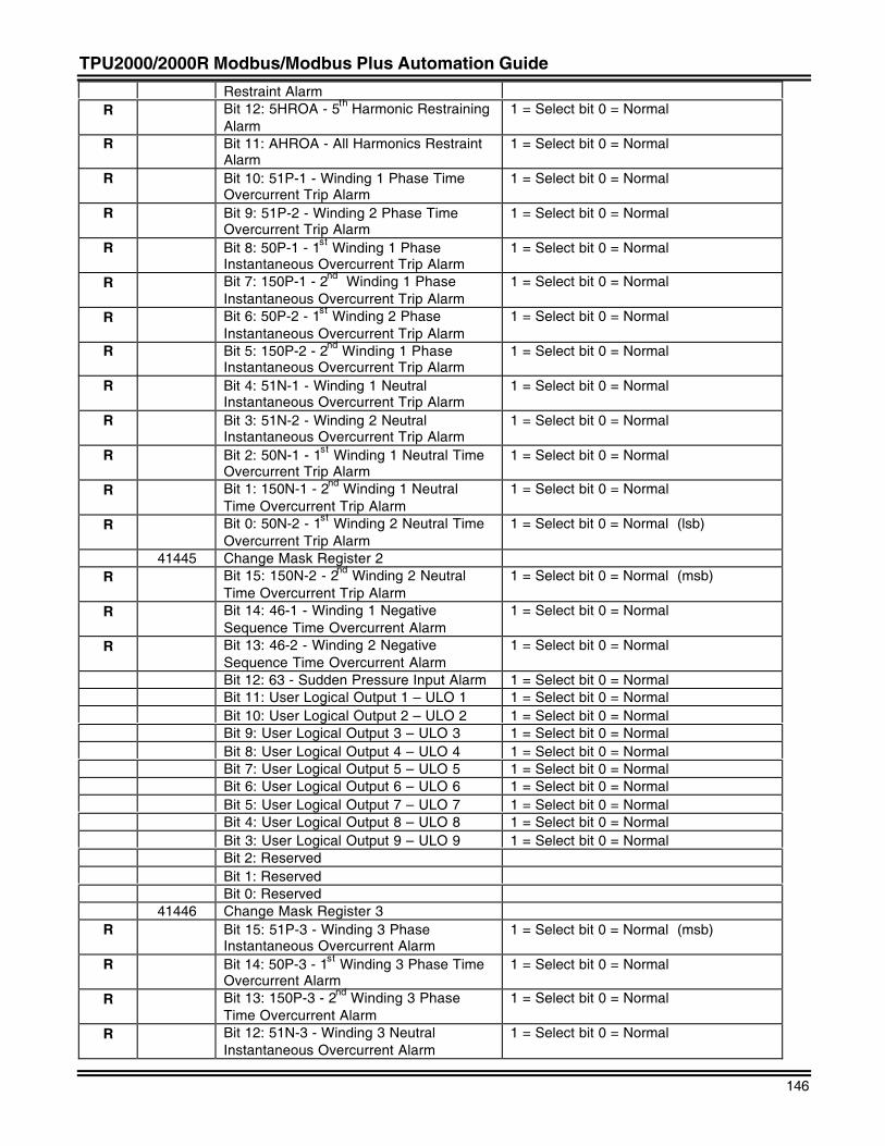
TPU2000/2000R Modbus/Modbus Plus Automation Guide
146
Restraint AlarmR Bit 12: 5HROA - 5th Harmonic Restraining
Alarm1 = Select bit 0 = Normal
R Bit 11: AHROA - All Harmonics RestraintAlarm
1 = Select bit 0 = Normal
R Bit 10: 51P-1 - Winding 1 Phase TimeOvercurrent Trip Alarm
1 = Select bit 0 = Normal
R Bit 9: 51P-2 - Winding 2 Phase TimeOvercurrent Trip Alarm
1 = Select bit 0 = Normal
R Bit 8: 50P-1 - 1st Winding 1 PhaseInstantaneous Overcurrent Trip Alarm
1 = Select bit 0 = Normal
R Bit 7: 150P-1 - 2nd Winding 1 PhaseInstantaneous Overcurrent Trip Alarm
1 = Select bit 0 = Normal
R Bit 6: 50P-2 - 1st Winding 2 PhaseInstantaneous Overcurrent Trip Alarm
1 = Select bit 0 = Normal
R Bit 5: 150P-2 - 2nd Winding 1 PhaseInstantaneous Overcurrent Trip Alarm
1 = Select bit 0 = Normal
R Bit 4: 51N-1 - Winding 1 NeutralInstantaneous Overcurrent Trip Alarm
1 = Select bit 0 = Normal
R Bit 3: 51N-2 - Winding 2 NeutralInstantaneous Overcurrent Trip Alarm
1 = Select bit 0 = Normal
R Bit 2: 50N-1 - 1st Winding 1 Neutral TimeOvercurrent Trip Alarm
1 = Select bit 0 = Normal
R Bit 1: 150N-1 - 2nd Winding 1 NeutralTime Overcurrent Trip Alarm
1 = Select bit 0 = Normal
R Bit 0: 50N-2 - 1st Winding 2 Neutral TimeOvercurrent Trip Alarm
1 = Select bit 0 = Normal (lsb)
41445 Change Mask Register 2R Bit 15: 150N-2 - 2nd Winding 2 Neutral
Time Overcurrent Trip Alarm1 = Select bit 0 = Normal (msb)
R Bit 14: 46-1 - Winding 1 NegativeSequence Time Overcurrent Alarm
1 = Select bit 0 = Normal
R Bit 13: 46-2 - Winding 2 NegativeSequence Time Overcurrent Alarm
1 = Select bit 0 = Normal
Bit 12: 63 - Sudden Pressure Input Alarm 1 = Select bit 0 = NormalBit 11: User Logical Output 1 – ULO 1 1 = Select bit 0 = NormalBit 10: User Logical Output 2 – ULO 2 1 = Select bit 0 = NormalBit 9: User Logical Output 3 – ULO 3 1 = Select bit 0 = NormalBit 8: User Logical Output 4 – ULO 4 1 = Select bit 0 = NormalBit 7: User Logical Output 5 – ULO 5 1 = Select bit 0 = NormalBit 6: User Logical Output 6 – ULO 6 1 = Select bit 0 = NormalBit 5: User Logical Output 7 – ULO 7 1 = Select bit 0 = NormalBit 4: User Logical Output 8 – ULO 8 1 = Select bit 0 = NormalBit 3: User Logical Output 9 – ULO 9 1 = Select bit 0 = NormalBit 2: ReservedBit 1: ReservedBit 0: Reserved
41446 Change Mask Register 3R Bit 15: 51P-3 - Winding 3 Phase
Instantaneous Overcurrent Alarm1 = Select bit 0 = Normal (msb)
R Bit 14: 50P-3 - 1st Winding 3 Phase TimeOvercurrent Alarm
1 = Select bit 0 = Normal
R Bit 13: 150P-3 - 2nd Winding 3 PhaseTime Overcurrent Alarm
1 = Select bit 0 = Normal
R Bit 12: 51N-3 - Winding 3 NeutralInstantaneous Overcurrent Alarm
1 = Select bit 0 = Normal
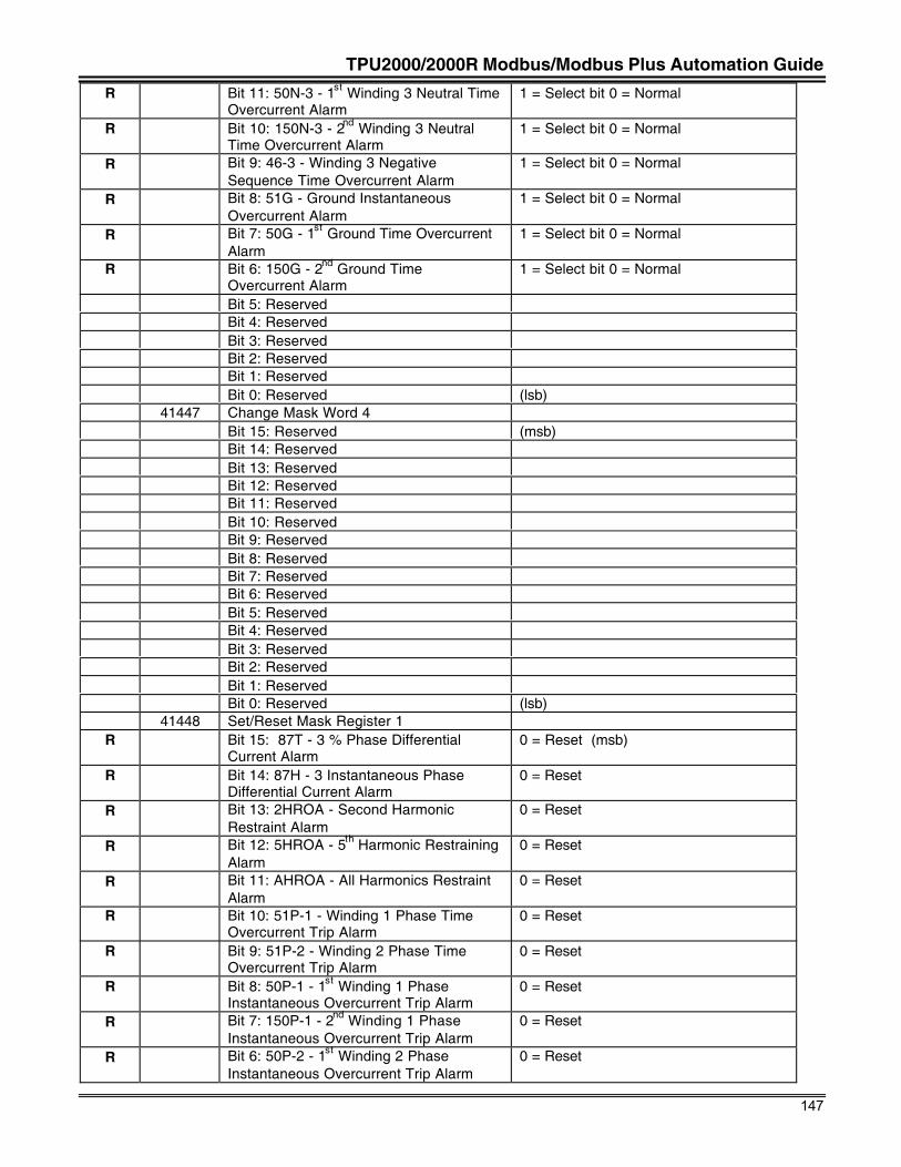
TPU2000/2000R Modbus/Modbus Plus Automation Guide
147
R Bit 11: 50N-3 - 1st Winding 3 Neutral TimeOvercurrent Alarm
1 = Select bit 0 = Normal
R Bit 10: 150N-3 - 2nd Winding 3 NeutralTime Overcurrent Alarm
1 = Select bit 0 = Normal
R Bit 9: 46-3 - Winding 3 NegativeSequence Time Overcurrent Alarm
1 = Select bit 0 = Normal
R Bit 8: 51G - Ground InstantaneousOvercurrent Alarm
1 = Select bit 0 = Normal
R Bit 7: 50G - 1st Ground Time OvercurrentAlarm
1 = Select bit 0 = Normal
R Bit 6: 150G - 2nd Ground TimeOvercurrent Alarm
1 = Select bit 0 = Normal
Bit 5: ReservedBit 4: ReservedBit 3: ReservedBit 2: ReservedBit 1: ReservedBit 0: Reserved (lsb)
41447 Change Mask Word 4Bit 15: Reserved (msb)Bit 14: ReservedBit 13: ReservedBit 12: ReservedBit 11: ReservedBit 10: ReservedBit 9: ReservedBit 8: ReservedBit 7: ReservedBit 6: ReservedBit 5: ReservedBit 4: ReservedBit 3: ReservedBit 2: ReservedBit 1: ReservedBit 0: Reserved (lsb)
41448 Set/Reset Mask Register 1R Bit 15: 87T - 3 % Phase Differential
Current Alarm0 = Reset (msb)
R Bit 14: 87H - 3 Instantaneous PhaseDifferential Current Alarm
0 = Reset
R Bit 13: 2HROA - Second HarmonicRestraint Alarm
0 = Reset
R Bit 12: 5HROA - 5th Harmonic RestrainingAlarm
0 = Reset
R Bit 11: AHROA - All Harmonics RestraintAlarm
0 = Reset
R Bit 10: 51P-1 - Winding 1 Phase TimeOvercurrent Trip Alarm
0 = Reset
R Bit 9: 51P-2 - Winding 2 Phase TimeOvercurrent Trip Alarm
0 = Reset
R Bit 8: 50P-1 - 1st Winding 1 PhaseInstantaneous Overcurrent Trip Alarm
0 = Reset
R Bit 7: 150P-1 - 2nd Winding 1 PhaseInstantaneous Overcurrent Trip Alarm
0 = Reset
R Bit 6: 50P-2 - 1st Winding 2 PhaseInstantaneous Overcurrent Trip Alarm
0 = Reset
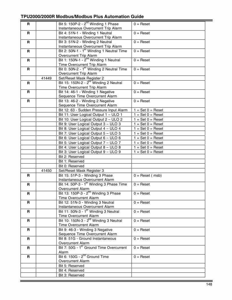
TPU2000/2000R Modbus/Modbus Plus Automation Guide
148
R Bit 5: 150P-2 - 2nd Winding 1 PhaseInstantaneous Overcurrent Trip Alarm
0 = Reset
R Bit 4: 51N-1 - Winding 1 NeutralInstantaneous Overcurrent Trip Alarm
0 = Reset
R Bit 3: 51N-2 - Winding 2 NeutralInstantaneous Overcurrent Trip Alarm
0 = Reset
R Bit 2: 50N-1 - 1st Winding 1 Neutral TimeOvercurrent Trip Alarm
0 = Reset
R Bit 1: 150N-1 - 2nd Winding 1 NeutralTime Overcurrent Trip Alarm
0 = Reset
R Bit 0: 50N-2 - 1st Winding 2 Neutral TimeOvercurrent Trip Alarm
0 = Reset
41449 Set/Reset Mask Register 2R Bit 15: 150N-2 - 2nd Winding 2 Neutral
Time Overcurrent Trip Alarm0 = Reset
R Bit 14: 46-1 - Winding 1 NegativeSequence Time Overcurrent Alarm
0 = Reset
R Bit 13: 46-2 - Winding 2 NegativeSequence Time Overcurrent Alarm
0 = Reset
Bit 12: 63 - Sudden Pressure Input Alarm 1 = Set 0 = ResetBit 11: User Logical Output 1 – ULO 1 1 = Set 0 = ResetBit 10: User Logical Output 2 – ULO 2 1 = Set 0 = ResetBit 9: User Logical Output 3 – ULO 3 1 = Set 0 = ResetBit 8: User Logical Output 4 – ULO 4 1 = Set 0 = ResetBit 7: User Logical Output 5 – ULO 5 1 = Set 0 = ResetBit 6: User Logical Output 6 – ULO 6 1 = Set 0 = ResetBit 5: User Logical Output 7 – ULO 7 1 = Set 0 = ResetBit 4: User Logical Output 8 – ULO 8 1 = Set 0 = ResetBit 3: User Logical Output 9 – ULO 9 1 = Set 0 = ResetBit 2: ReservedBit 1: ReservedBit 0: Reserved
41450 Set/Reset Mask Register 3R Bit 15: 51P-3 - Winding 3 Phase
Instantaneous Overcurrent Alarm0 = Reset ( msb)
R Bit 14: 50P-3 - 1st Winding 3 Phase TimeOvercurrent Alarm
0 = Reset
R Bit 13: 150P-3 - 2nd Winding 3 PhaseTime Overcurrent Alarm
0 = Reset
R Bit 12: 51N-3 - Winding 3 NeutralInstantaneous Overcurrent Alarm
0 = Reset
R Bit 11: 50N-3 - 1st Winding 3 NeutralTime Overcurrent Alarm
0 = Reset
R Bit 10: 150N-3 - 2nd Winding 3 NeutralTime Overcurrent Alarm
0 = Reset
R Bit 9: 46-3 - Winding 3 NegativeSequence Time Overcurrent Alarm
0 = Reset
R Bit 8: 51G - Ground InstantaneousOvercurrent Alarm
0 = Reset
R Bit 7: 50G - 1st Ground Time OvercurrentAlarm
0 = Reset
R Bit 6: 150G - 2nd Ground TimeOvercurrent Alarm
0 = Reset
Bit 5: ReservedBit 4: ReservedBit 3: Reserved
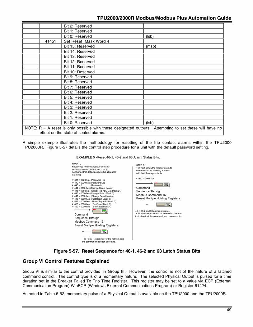
TPU2000/2000R Modbus/Modbus Plus Automation Guide
149
Bit 2: ReservedBit 1: ReservedBit 0: Reserved (lsb)
41451 Set Reset Mask Word 4Bit 15: Reserved (msb)Bit 14: ReservedBit 13: ReservedBit 12: ReservedBit 11: ReservedBit 10: ReservedBit 9: ReservedBit 8: ReservedBit 7: ReservedBit 6: ReservedBit 5: ReservedBit 4: ReservedBit 3: ReservedBit 2: ReservedBit 1: ReservedBit 0: Reserved (lsb)
NOTE: R = A reset is only possible with these designated outputs. Attempting to set these will have noeffect on the state of sealed alarms.
A simple example illustrates the methodology for resetting of the trip contact alarms within the TPU2000TPU2000R. Figure 5-57 details the control step procedure for a unit with the default password setting.
EC
CommandSequence ThroughModbus Command 16Preset Multiple Holding Registers
STEP 1 -Host sends following register contentsto initiate a reset of 46-1, 46-2, an 63( Assumed that defaultpassword of all spaces is active).
41441 = 2020 hex (Password Hi)41442 = 2020 hex (Password Lo)41443 = 0 (Reserved)41444 = 0000 hex (Change Select Mask 1)41445 = 7000 hex (Select Trip ABC Bits Mask 2).41446 = 0000 hex (Change Select Mask 3)41447 = 0800 hex (Change Select Mask 4)41448 = 0000 hex ( Set/Reset Mask 1)41449 = 0000 hex (Reset Trip ABC Mask 2)41450 = 0000 hex ( Set/Reset Mask 3)41452 = 0000 hex ( Set/Reset Mask 4)
EXAMPLE 5 -Reset 46-1, 46-2 and 63 Alarm Status Bits.
EC
46-1, 46-2 and 63 alarms are reset. A Modbus response will be returned to the hostindicating that the command has been accepted.
EC
CommandSequence ThroughModbus Command 16Preset Multiple Holding Registers
STEP 2 -The host sends the register executecommand to the following address with the following contents.
41452 = 0001 hex
EC
The Relay Responds over the network that the command has been accepted.
Figure 5-57. Reset Sequence for 46-1, 46-2 and 63 Latch Status Bits
Group VI Control Features Explained
Group VI is similar to the control provided in Group III. However, the control is not of the nature of a latchedcommand control. The control type is of a momentary nature. The selected Physical Output is pulsed for a timeduration set in the Breaker Failed To Trip Time Register. This register may be set to a value via ECP (ExternalCommunication Program) WinECP (Windows External Communications Program) or Register 61424.
As noted in Table 5-52, momentary pulse of a Physical Output is available on the TPU2000 and the TPU2000R.
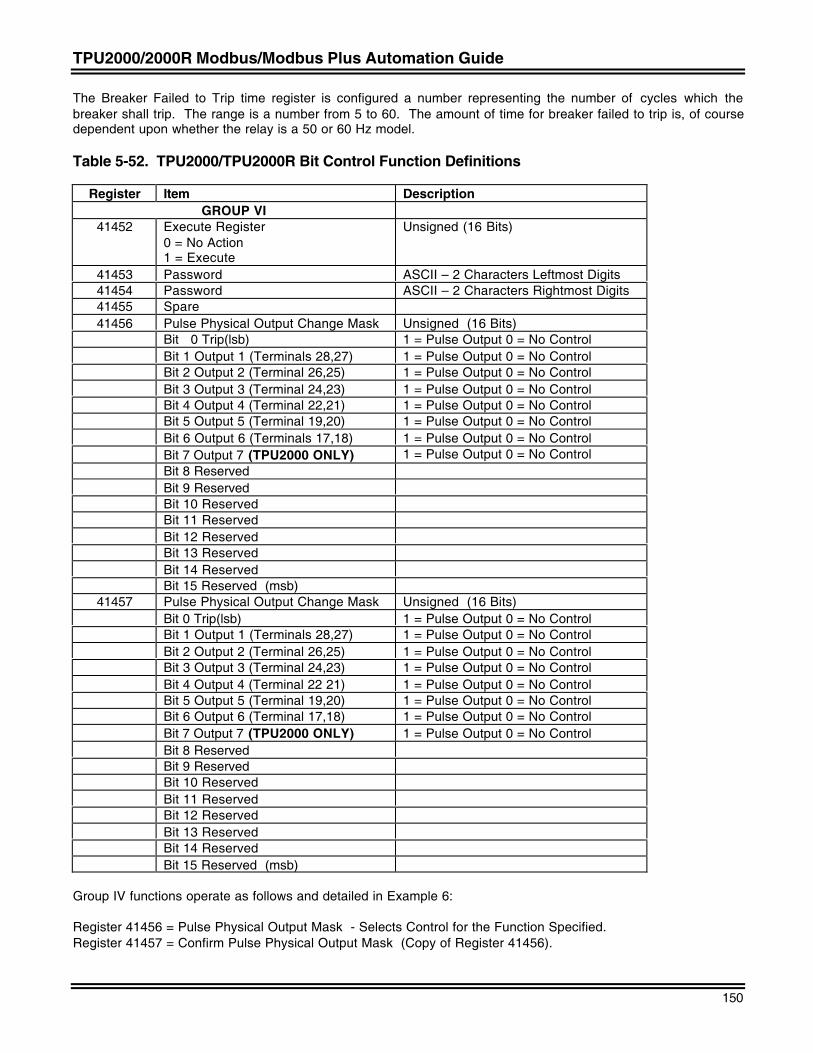
TPU2000/2000R Modbus/Modbus Plus Automation Guide
150
The Breaker Failed to Trip time register is configured a number representing the number of cycles which thebreaker shall trip. The range is a number from 5 to 60. The amount of time for breaker failed to trip is, of coursedependent upon whether the relay is a 50 or 60 Hz model.
Table 5-52. TPU2000/TPU2000R Bit Control Function Definitions
Register Item DescriptionGROUP VI
41452 Execute Register0 = No Action1 = Execute
Unsigned (16 Bits)
41453 Password ASCII – 2 Characters Leftmost Digits41454 Password ASCII – 2 Characters Rightmost Digits41455 Spare41456 Pulse Physical Output Change Mask Unsigned (16 Bits)
Bit 0 Trip(lsb) 1 = Pulse Output 0 = No ControlBit 1 Output 1 (Terminals 28,27) 1 = Pulse Output 0 = No ControlBit 2 Output 2 (Terminal 26,25) 1 = Pulse Output 0 = No ControlBit 3 Output 3 (Terminal 24,23) 1 = Pulse Output 0 = No ControlBit 4 Output 4 (Terminal 22,21) 1 = Pulse Output 0 = No ControlBit 5 Output 5 (Terminal 19,20) 1 = Pulse Output 0 = No ControlBit 6 Output 6 (Terminals 17,18) 1 = Pulse Output 0 = No ControlBit 7 Output 7 (TPU2000 ONLY) 1 = Pulse Output 0 = No ControlBit 8 ReservedBit 9 ReservedBit 10 ReservedBit 11 ReservedBit 12 ReservedBit 13 ReservedBit 14 ReservedBit 15 Reserved (msb)
41457 Pulse Physical Output Change Mask Unsigned (16 Bits)Bit 0 Trip(lsb) 1 = Pulse Output 0 = No ControlBit 1 Output 1 (Terminals 28,27) 1 = Pulse Output 0 = No ControlBit 2 Output 2 (Terminal 26,25) 1 = Pulse Output 0 = No ControlBit 3 Output 3 (Terminal 24,23) 1 = Pulse Output 0 = No ControlBit 4 Output 4 (Terminal 22 21) 1 = Pulse Output 0 = No ControlBit 5 Output 5 (Terminal 19,20) 1 = Pulse Output 0 = No ControlBit 6 Output 6 (Terminal 17,18) 1 = Pulse Output 0 = No ControlBit 7 Output 7 (TPU2000 ONLY) 1 = Pulse Output 0 = No ControlBit 8 ReservedBit 9 ReservedBit 10 ReservedBit 11 ReservedBit 12 ReservedBit 13 ReservedBit 14 ReservedBit 15 Reserved (msb)
Group IV functions operate as follows and detailed in Example 6:
Register 41456 = Pulse Physical Output Mask - Selects Control for the Function Specified.Register 41457 = Confirm Pulse Physical Output Mask (Copy of Register 41456).
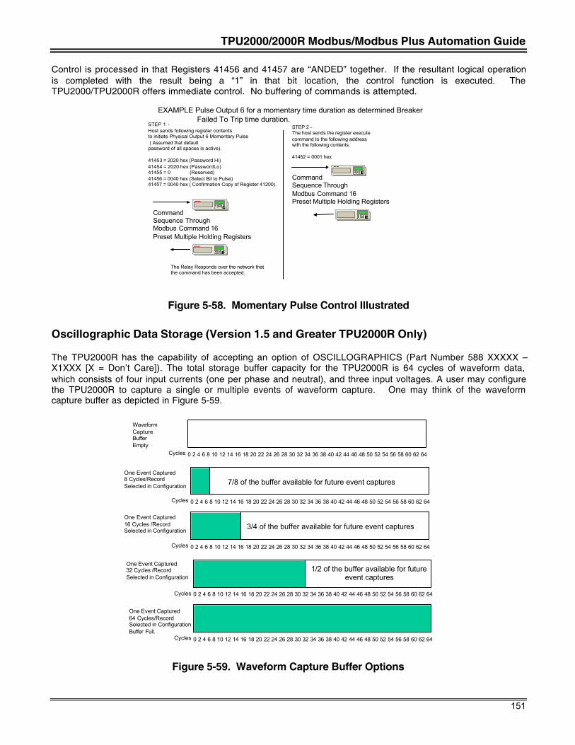
TPU2000/2000R Modbus/Modbus Plus Automation Guide
151
Control is processed in that Registers 41456 and 41457 are “ANDED” together. If the resultant logical operationis completed with the result being a “1” in that bit location, the control function is executed. TheTPU2000/TPU2000R offers immediate control. No buffering of commands is attempted.
EC
CommandSequence ThroughModbus Command 16Preset Multiple Holding Registers
STEP 1 -Host sends following register contentsto initiate Physical Output 6 Momentary Pulse ( Assumed that defaultpassword of all spaces is active).
41453 = 2020 hex (Password Hi)41454 = 2020 hex (Password Lo)41455 = 0 (Reserved)41456 = 0040 hex (Select Bit to Pulse)41457 = 0040 hex ( Confirmation Copy of Register 41200).
EXAMPLE Pulse Output 6 for a momentary time duration as determined Breaker Failed To Trip time duration.
EC
EC
CommandSequence ThroughModbus Command 16Preset Multiple Holding Registers
STEP 2 -The host sends the register executecommand to the following address with the following contents.
41452 = 0001 hex
EC
The Relay Responds over the network that the command has been accepted.
Figure 5-58. Momentary Pulse Control Illustrated
Oscillographic Data Storage (Version 1.5 and Greater TPU2000R Only)
The TPU2000R has the capability of accepting an option of OSCILLOGRAPHICS (Part Number 588 XXXXX –X1XXX [X = Don’t Care]). The total storage buffer capacity for the TPU2000R is 64 cycles of waveform data,which consists of four input currents (one per phase and neutral), and three input voltages. A user may configurethe TPU2000R to capture a single or multiple events of waveform capture. One may think of the waveformcapture buffer as depicted in Figure 5-59.
WaveformCaptureBufferEmpty
0 2 4 6 8 10 12 14 16 18 20 22 24 26 28 30 32 34 36 38 40 42 44 46 48 50 52 54 56 58 60 62 64Cycles
0 2 4 6 8 10 12 14 16 18 20 22 24 26 28 30 32 34 36 38 40 42 44 46 48 50 52 54 56 58 60 62 64Cycles
0 2 4 6 8 10 12 14 16 18 20 22 24 26 28 30 32 34 36 38 40 42 44 46 48 50 52 54 56 58 60 62 64Cycles
0 2 4 6 8 10 12 14 16 18 20 22 24 26 28 30 32 34 36 38 40 42 44 46 48 50 52 54 56 58 60 62 64Cycles
0 2 4 6 8 10 12 14 16 18 20 22 24 26 28 30 32 34 36 38 40 42 44 46 48 50 52 54 56 58 60 62 64Cycles
7/8 of the buffer available for future event captures
3/4 of the buffer available for future event captures
One Event Captured32 Cycles /RecordSelected in Configuration
1/2 of the buffer available for future event captures
One Event Captured64 Cycles/Record Selected in ConfigurationBuffer Full.
One Event Captured8 Cycles/Record Selected in Configuration
One Event Captured16 Cycles /Record Selected in Configuration
Figure 5-59. Waveform Capture Buffer Options
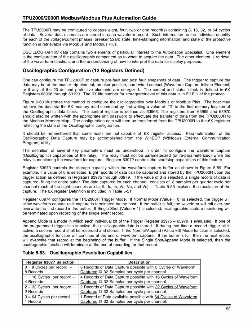
TPU2000/2000R Modbus/Modbus Plus Automation Guide
152
The TPU2000R may be configured to capture eight, four, two or one record(s) containing 8, 16, 32, or 64 cyclesof data. Several data elements are stored in each waveform record. Such information as the individual quantityfor each of the voltage/current phases, breaker 52a/b state, time-stamping information, and state of the protectivefunction is retrievable via Modbus and Modbus Plus.
OSCILLOGRAPHIC data contains two elements of particular interest to the Automation Specialist. One elementis the configuration of the oscillographic component as to when to acquire the data. The other element is retrievalof the wave form functions and the understanding of how to interpret the data for display purposes.
Oscillographic Configuration (12 Registers Defined)
One can configure the TPU2000R to capture pre-fault and post fault snapshots of data. The trigger to capture thedata may be of the master trip element, breaker position, hard wired contact (Waveform Capture Initiate Element)or if any of the 20 defined protective elements are energized. The control and status block is defined in 6XRegisters 63968 through 63199. The 6X file number for storage/retrieval of this data is in FILE 1 of the protocol.
Figure 5-60 illustrates the method to configure the oscillographics over Modbus or Modbus Plus. The host mayretrieve the data via the 6X memory read command by first writing a value of “2” to the first memory location ofthe Oscillographic data block. The control register is defined as 63968. The registers from 63969 and 63970should also be written with the appropriate unit password to effectuate the transfer of data from the TPU2000R tothe Modbus Memory Map. The configuration data will then be transferred from the TPU2000R to the 6X registersreflecting the state of the Oscillographic configuration.
It should be remembered that some hosts are not capable of 6X register access. Parameterization of theOscillographic Data Capture may be accomplished from the WinECP (WINdows External CommunicationProgram) utility.
The definition of several key parameters must be understood in order to configure the waveform capture(Oscillographic) capabilities of the relay. The relay must not be parameterized (or re-parameterized) while therelay is monitoring the waveform for capture. Register 63972 controls the start/stop capabilities of this feature.
Register 63973 controls the storage capacity within the waveform capture buffer as shown in Figure 5-59. Forexample, if a value of 0 is selected, Eight records of data can be captured and stored by the TPU2000R upon thetrigger action as defined in Registers 63975 through 63979. If the value of 3 is selected, a single record of data iscaptured, filling the entire buffer. The data captured for each channel consists of 8 samples per quarter cycle perchannel (each of the eight channels are Ia, Ib, Ic, In, Va, Vb, and Vc). Table 5-53 explains the resolution of thecapture. The 6X register Definition is included in Table 5-51.
Register 63974 configures the TPU2000R Trigger Mode. If Normal Mode (Value = 0) is selected, the trigger willallow waveform capture until capture is terminated by the host. If the buffer is full, the waveform will roll over andoverwrite the first record in the buffer. If Single Shot (Value = 1) is selected, oscillographic capture monitoring willbe terminated upon recording of the single event record.
Append Mode is a mode in which each individual bit of the Trigger Register 63975 – 63979 is evaluated. If one ofthe programmed trigger bits is active, the oscillographic data is stored. If during that time a second trigger bit isactive, a second record shall be recorded and stored. If the Normal/Append (Value =3) Mode function is selected,the oscillographic function will continue at the end of waveform capture. If the buffer is full, then the next recordwill overwrite that record at the beginning of the buffer. If the Single Shot/Append Mode is selected, then theoscillographic function will terminate at the end of recording for that record.
Table 5-53. Oscillographic Resolution Capabilities
Register 63077 Selection Description0 = 8 Cycles per record –8 Records
8 Records of Data Capture possible with 8 Cycles of WaveformCaptured @ 32 Samples per cycle per channel.
1 = 16 Cycles per record –4 Records
4 Records of Data Capture possible with 16 Cycles of WaveformCaptured @ 32 Samples per cycle per channel.
2 = 32 Cycles per record –2 Records
2 Records of Data Capture possible with 32 Cycles of WaveformCaptured @ 32 Samples per cycle per channel.
3 = 64 Cycles per record –1 Record
1 Record of Data available possible with 64 Cycles of WaveformCaptured @ 32 Samples per cycle per channel.
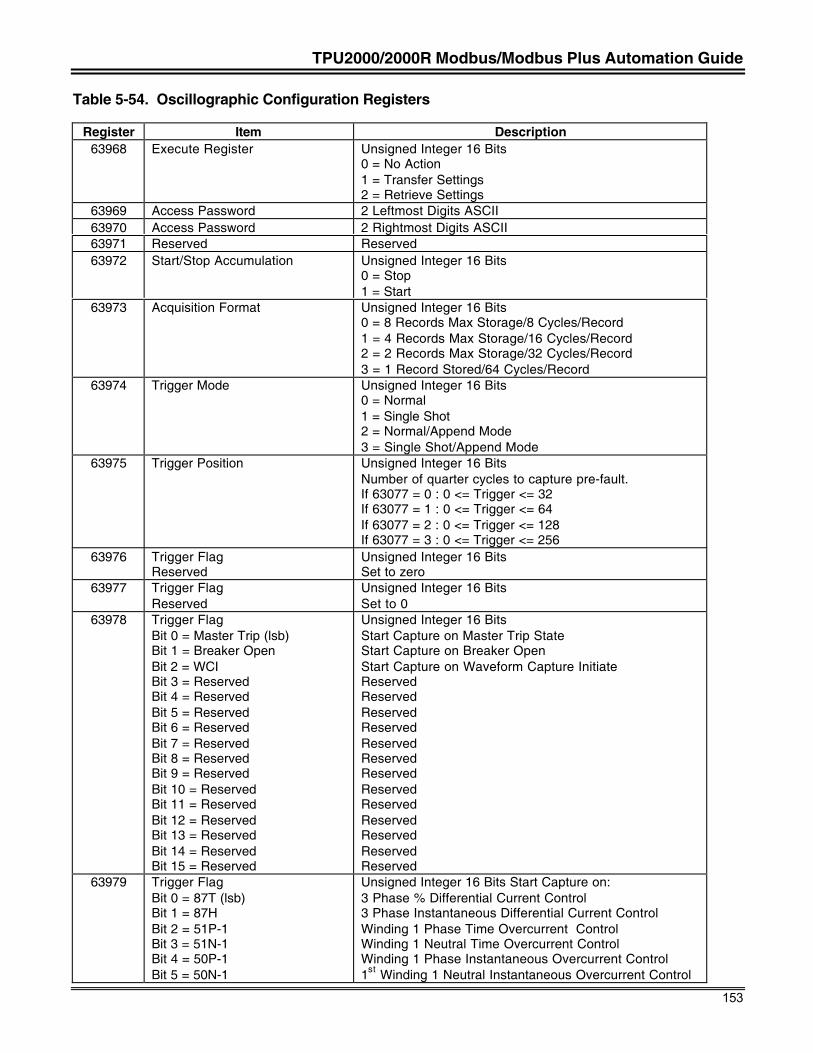
TPU2000/2000R Modbus/Modbus Plus Automation Guide
153
Table 5-54. Oscillographic Configuration Registers
Register Item Description63968 Execute Register Unsigned Integer 16 Bits
0 = No Action1 = Transfer Settings2 = Retrieve Settings
63969 Access Password 2 Leftmost Digits ASCII63970 Access Password 2 Rightmost Digits ASCII63971 Reserved Reserved63972 Start/Stop Accumulation Unsigned Integer 16 Bits
0 = Stop1 = Start
63973 Acquisition Format Unsigned Integer 16 Bits0 = 8 Records Max Storage/8 Cycles/Record1 = 4 Records Max Storage/16 Cycles/Record2 = 2 Records Max Storage/32 Cycles/Record3 = 1 Record Stored/64 Cycles/Record
63974 Trigger Mode Unsigned Integer 16 Bits0 = Normal1 = Single Shot2 = Normal/Append Mode3 = Single Shot/Append Mode
63975 Trigger Position Unsigned Integer 16 BitsNumber of quarter cycles to capture pre-fault.If 63077 = 0 : 0 <= Trigger <= 32If 63077 = 1 : 0 <= Trigger <= 64If 63077 = 2 : 0 <= Trigger <= 128If 63077 = 3 : 0 <= Trigger <= 256
63976 Trigger FlagReserved
Unsigned Integer 16 BitsSet to zero
63977 Trigger FlagReserved
Unsigned Integer 16 BitsSet to 0
63978 Trigger FlagBit 0 = Master Trip (lsb)Bit 1 = Breaker OpenBit 2 = WCIBit 3 = ReservedBit 4 = ReservedBit 5 = ReservedBit 6 = ReservedBit 7 = ReservedBit 8 = ReservedBit 9 = ReservedBit 10 = ReservedBit 11 = ReservedBit 12 = ReservedBit 13 = ReservedBit 14 = ReservedBit 15 = Reserved
Unsigned Integer 16 BitsStart Capture on Master Trip StateStart Capture on Breaker OpenStart Capture on Waveform Capture InitiateReservedReservedReservedReservedReservedReservedReservedReservedReservedReservedReservedReservedReserved
63979 Trigger FlagBit 0 = 87T (lsb)Bit 1 = 87HBit 2 = 51P-1Bit 3 = 51N-1Bit 4 = 50P-1Bit 5 = 50N-1
Unsigned Integer 16 Bits Start Capture on:3 Phase % Differential Current Control3 Phase Instantaneous Differential Current ControlWinding 1 Phase Time Overcurrent ControlWinding 1 Neutral Time Overcurrent ControlWinding 1 Phase Instantaneous Overcurrent Control1st Winding 1 Neutral Instantaneous Overcurrent Control
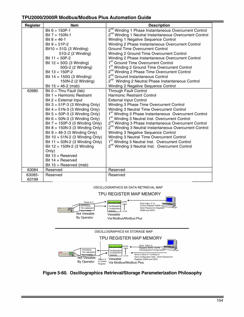
TPU2000/2000R Modbus/Modbus Plus Automation Guide
154
Register Item DescriptionBit 6 = 150P-1Bit 7 = 150N-1Bit 8 = 46-1Bit 9 = 51P-2Bit10 = 51G (3 Winding) 51G-2 (2 Winding)Bit 11 = 50P-2Bit 12 = 50G (3 Winding) 50G-2 (2 Winding)Bit 13 = 150P-2Bit 14 = 150G (3 Winding) 150N-2 (2 Winding)Bit 15 = 46-2 (msb)
2nd Winding 1 Phase Instantaneous Overcurrent Control2nd Winding 1 Neutral Instantaneous Overcurrent ControlWinding 1 Negative Sequence ControlWinding 2 Phase Instantaneous Overcurrent ControlGround Time Overcurrent ControlWinding 2 Ground Time Overcurrent ControlWinding 2 Phase Instantaneous Overcurrent Control1st Ground Time Overcurrent Control1st Winding 2 Ground Time Overcurrent Control2nd Winding 2 Phase Time Overcurrent Control2nd Ground Instantaneous Control2nd Winding 2 Neutral Phase Instantaneous ControlWinding 2 Negative Sequence Control
63980 Bit 0 = Thru Fault (lsb)Bit 1 = Harmonic RestraintBit 2 = External InputBit 3 = 51P-3 (3 Winding Only)Bit 4 = 51N-3 (3 Winding Only)Bit 5 = 50P-3 (3 Winding Only)Bit 6 = 50N-3 (3 Winding Only)Bit 7 = 150P-3 (3 Winding Only)Bit 8 = 150N-3 (3 Winding Only)Bit 9 = 46-3 (3 Winding Only)Bit 10 = 51N-2 (3 Winding Only)Bit 11 = 50N-2 (3 Winding Only)Bit 12 = 150N-2 (3 WindingOnly)Bit 13 = ReservedBit 14 = ReservedBit 15 = Reserved (msb)
Through Fault ControlHarmonic Restraint ControlExternal Input ControlWinding 3 Phase Time Overcurrent ControlWinding 3 Neutral Time Overcurrent Control1st Winding 3 Phase Instantaneous Overcurrent Control1st Winding 3 Neutral Inst. Overcurrent Control2nd Winding 3 Phase Instantaneous Overcurrent Control2nd Winding 3 Neutral Instantaneous Overcurrent ControlWinding 3 Negative Sequence ControlWinding 3 Neutral Time Overcurrent Control1st Winding 3 Neutral Inst. Overcurrent Control2nd Winding 3 Neutral Inst. Overcurrent Control
63084 Reserved Reserved63085-63199
Reserved Reserved
OSCILLOGRAPHICS 6X DATA RETRIEVAL MAP
TPU REGISTER MAP MEMORY
Data Control Register
OscillographicConfigurationSettings
63968
63969
63199EC
INTERNALTPU MEMORYNon-Volatile
Send Value “2” toControl Register 63968Send Password to Registers63969 and 63970
Not ViewableBy Operator
Viewable Via Modbus/Modbus Plus
OSCILLOGRAPHICS 6X STORAGE MAP
TPU REGISTER MAP MEMORY
Data Control Register
OscillographicConfigurationSettings
6396863969
63199
. .
EC
INTERNALTPU MEMORYNon-Volatile
Send “Data” toRegisters 63972 -63199 (Oscillographic Configuration)
Not ViewableBy Operator
Viewable Via Modbus/Modbus Plus
Reset to 0.
Send a Value of 1 to Relay toSave Configuration Data. Send Password toRegisters 63969 and 63970Write a 0
to ControlRegister
Figure 5-60. Oscillographics Retrieval/Storage Parameterization Philosophy
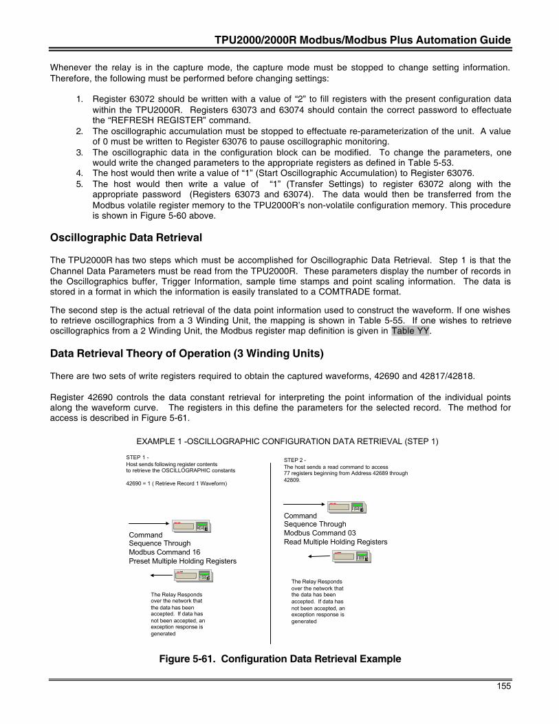
TPU2000/2000R Modbus/Modbus Plus Automation Guide
155
Whenever the relay is in the capture mode, the capture mode must be stopped to change setting information.Therefore, the following must be performed before changing settings:
1. Register 63072 should be written with a value of “2” to fill registers with the present configuration datawithin the TPU2000R. Registers 63073 and 63074 should contain the correct password to effectuatethe “REFRESH REGISTER” command.
2. The oscillographic accumulation must be stopped to effectuate re-parameterization of the unit. A valueof 0 must be written to Register 63076 to pause oscillographic monitoring.
3. The oscillographic data in the configuration block can be modified. To change the parameters, onewould write the changed parameters to the appropriate registers as defined in Table 5-53.
4. The host would then write a value of “1” (Start Oscillographic Accumulation) to Register 63076.5. The host would then write a value of “1” (Transfer Settings) to register 63072 along with the
appropriate password (Registers 63073 and 63074). The data would then be transferred from theModbus volatile register memory to the TPU2000R’s non-volatile configuration memory. This procedureis shown in Figure 5-60 above.
Oscillographic Data Retrieval
The TPU2000R has two steps which must be accomplished for Oscillographic Data Retrieval. Step 1 is that theChannel Data Parameters must be read from the TPU2000R. These parameters display the number of records inthe Oscillographics buffer, Trigger Information, sample time stamps and point scaling information. The data isstored in a format in which the information is easily translated to a COMTRADE format.
The second step is the actual retrieval of the data point information used to construct the waveform. If one wishesto retrieve oscillographics from a 3 Winding Unit, the mapping is shown in Table 5-55. If one wishes to retrieveoscillographics from a 2 Winding Unit, the Modbus register map definition is given in Table YY.
Data Retrieval Theory of Operation (3 Winding Units)
There are two sets of write registers required to obtain the captured waveforms, 42690 and 42817/42818.
Register 42690 controls the data constant retrieval for interpreting the point information of the individual pointsalong the waveform curve. The registers in this define the parameters for the selected record. The method foraccess is described in Figure 5-61.
EC
CommandSequence ThroughModbus Command 16Preset Multiple Holding Registers
STEP 1 -Host sends following register contentsto retrieve the OSCILLOGRAPHIC constants
42690 = 1 ( Retrieve Record 1 Waveform)
EXAMPLE 1 -OSCILLOGRAPHIC CONFIGURATION DATA RETRIEVAL (STEP 1)
EC
EC
CommandSequence ThroughModbus Command 03Read Multiple Holding Registers
STEP 2 -The host sends a read command to access77 registers beginning from Address 42689 through 42809.
EC
The Relay Respondsover the network that the data has been accepted. If data has not been accepted, anexception response isgenerated
The Relay Respondsover the network that the data has been accepted. If data has not been accepted, anexception response isgenerated
Figure 5-61. Configuration Data Retrieval Example
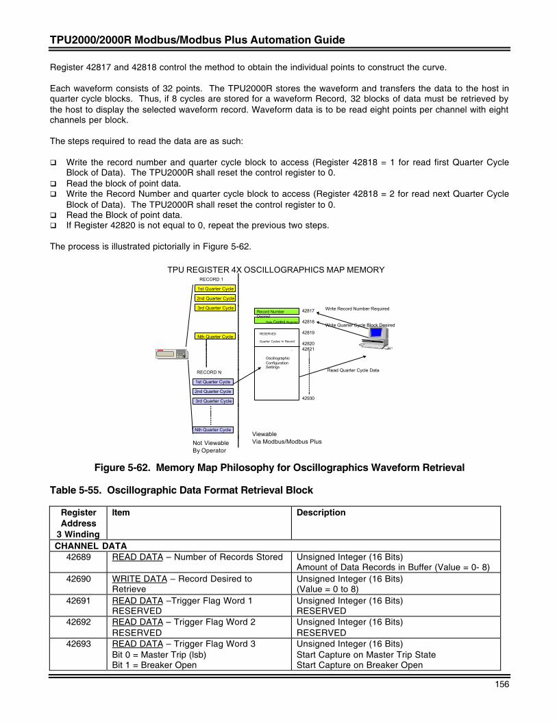
TPU2000/2000R Modbus/Modbus Plus Automation Guide
156
Register 42817 and 42818 control the method to obtain the individual points to construct the curve.
Each waveform consists of 32 points. The TPU2000R stores the waveform and transfers the data to the host inquarter cycle blocks. Thus, if 8 cycles are stored for a waveform Record, 32 blocks of data must be retrieved bythe host to display the selected waveform record. Waveform data is to be read eight points per channel with eightchannels per block.
The steps required to read the data are as such:
q Write the record number and quarter cycle block to access (Register 42818 = 1 for read first Quarter CycleBlock of Data). The TPU2000R shall reset the control register to 0.
q Read the block of point data.q Write the Record Number and quarter cycle block to access (Register 42818 = 2 for read next Quarter Cycle
Block of Data). The TPU2000R shall reset the control register to 0.q Read the Block of point data.q If Register 42820 is not equal to 0, repeat the previous two steps.
The process is illustrated pictorially in Figure 5-62.
TPU REGISTER 4X OSCILLOGRAPHICS MAP MEMORY
Data Control Register
OscillographicConfigurationSettings
..
EC
Not ViewableBy Operator
Viewable Via Modbus/Modbus Plus
Record NumberDesired
42817
42818
42819
4282042821
42930
RESERVED
Quarter Cycles In Record
1st Quarter Cycle
2nd Quarter Cycle
3rd Quarter Cycle
Nth Quarter Cycle
RECORD N
1st Quarter Cycle
2nd Quarter Cycle
3rd Quarter Cycle
Nth Quarter Cycle
RECORD 1
Write Record Number Required
Write Quarter Cycle Block Desired
Read Quarter Cycle Data
Figure 5-62. Memory Map Philosophy for Oscillographics Waveform Retrieval
Table 5-55. Oscillographic Data Format Retrieval Block
RegisterAddress
3 Winding
Item Description
CHANNEL DATA42689 READ DATA – Number of Records Stored Unsigned Integer (16 Bits)
Amount of Data Records in Buffer (Value = 0- 8)42690 WRITE DATA – Record Desired to
RetrieveUnsigned Integer (16 Bits)(Value = 0 to 8)
42691 READ DATA –Trigger Flag Word 1RESERVED
Unsigned Integer (16 Bits)RESERVED
42692 READ DATA – Trigger Flag Word 2RESERVED
Unsigned Integer (16 Bits)RESERVED
42693 READ DATA – Trigger Flag Word 3Bit 0 = Master Trip (lsb)Bit 1 = Breaker Open
Unsigned Integer (16 Bits)Start Capture on Master Trip StateStart Capture on Breaker Open
TPU2000/2000R Modbus/Modbus Plus Automation Guide
157
RegisterAddress
3 Winding
Item Description
Bit 2 = WCIBit 3 = ReservedBit 4 = ReservedBit 5 = ReservedBit 6 = ReservedBit 7 = ReservedBit 8 = ReservedBit 9 = ReservedBit 10 = ReservedBit 11 = ReservedBit 12 = ReservedBit 13 = ReservedBit 14 = ReservedBit 15 = Reserved (msb)
Start Capture on Waveform Capture InitiateReservedReservedReservedReservedReservedReservedReservedReservedReservedReservedReservedReservedReserved
42694 READ DATA – Trigger Flag Word 4Bit 0 = 50N-1 (lsb)Bit 1 = 50N-2Bit 2 = 50N-3Bit 3 = 51NBit 4 = 50P-1Bit 5 = 50P-2Bit 6 = 50P-3Bit 7 = 51PBit 8 = 67PBit 9 = 67NBit10 = 46Bit 11 = 27Bit 12 = 59Bit 13 = 79VBit 14 = 81S-1Bit 15 = 81R –1 (msb)
Unsigned Integer (16 Bits)Neutral. Instantaneous Overcurrent TripNeutral. Instantaneous Overcurrent TripNeutral. Instantaneous Overcurrent TripNeutral Time Overcurrent TripPhase Instantaneous Overcurrent TripPhase Instantaneous Overcurrent TripPhase Instantaneous Overcurrent Trip PhaseTime Overcurrent TripDirect Overcurrent Trip Positive SequenceDirect Overcurrent Trip Negative SequenceNegative Sequence Overcurrent TripUndervoltage TripOvercurrent TripRecloser LockoutFrequency Shed (First Stage)Frequency Restore (First Stage)
DATE/TIMESTAMPS OF TRIGGER POINT42695 Year Unsigned Integer 16 Bits
0-9942696 Month Unsigned Integer 16 Bits
1- 1242697 Day Unsigned Integer 16 bits
1-3142698 Hour Unsigned Integer 16 Bits
0-2342699 Minute Unsigned Integer 16 Bits
0-5942700 Second Unsigned Integer 16 Bits
0-5942701 Hundredths of Seconds Unsigned Integer 16 Bits
0 – 9942702 Quarter Cycle Trigger Point Unsigned Integer 16 Bits
Number of 1/4 Cycle of Trigger Point0-255 ( Dependent on 6X Register Config)
42703 Total Number of Channels Unsigned Integer 16 BitsDefault as 7
42704 Total Analog Data Channels Unsigned Integer 16 BitsFIXED at 7
42705 Total Digital Data Channels Unsigned Integer 16 Bits0 <=Range <= 64
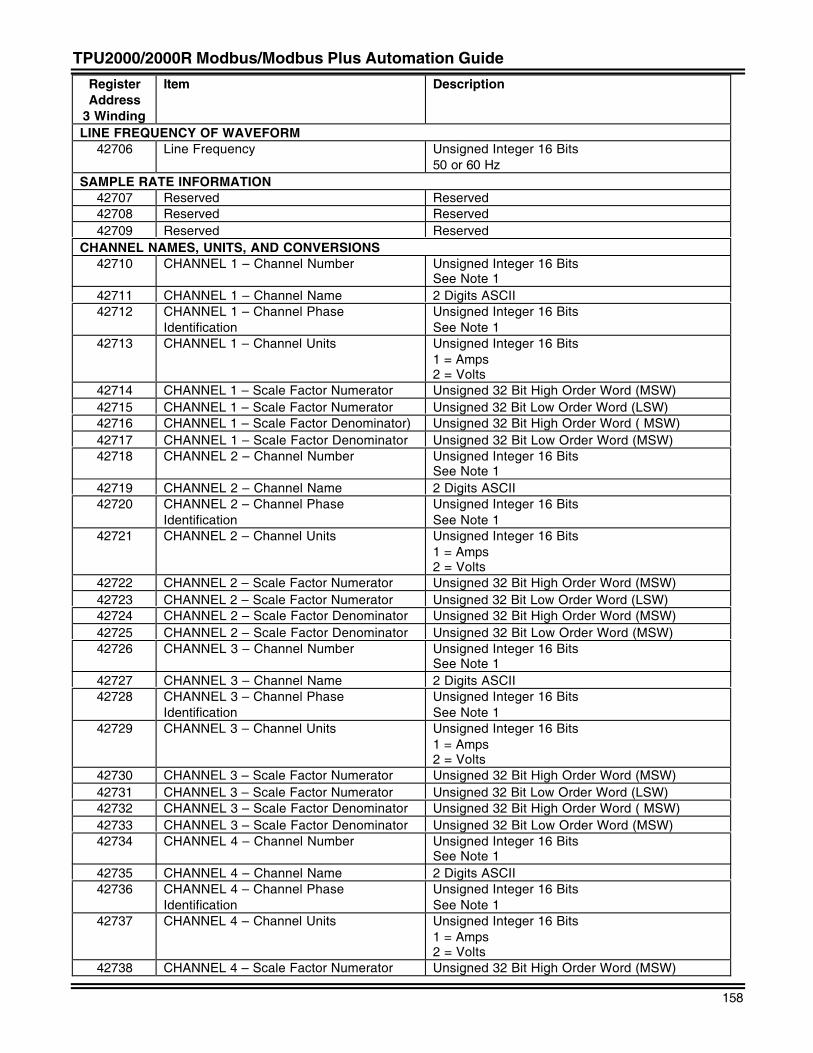
TPU2000/2000R Modbus/Modbus Plus Automation Guide
158
RegisterAddress
3 Winding
Item Description
LINE FREQUENCY OF WAVEFORM42706 Line Frequency Unsigned Integer 16 Bits
50 or 60 HzSAMPLE RATE INFORMATION
42707 Reserved Reserved42708 Reserved Reserved42709 Reserved Reserved
CHANNEL NAMES, UNITS, AND CONVERSIONS42710 CHANNEL 1 – Channel Number Unsigned Integer 16 Bits
See Note 142711 CHANNEL 1 – Channel Name 2 Digits ASCII42712 CHANNEL 1 – Channel Phase
IdentificationUnsigned Integer 16 BitsSee Note 1
42713 CHANNEL 1 – Channel Units Unsigned Integer 16 Bits1 = Amps2 = Volts
42714 CHANNEL 1 – Scale Factor Numerator Unsigned 32 Bit High Order Word (MSW)42715 CHANNEL 1 – Scale Factor Numerator Unsigned 32 Bit Low Order Word (LSW)42716 CHANNEL 1 – Scale Factor Denominator) Unsigned 32 Bit High Order Word ( MSW)42717 CHANNEL 1 – Scale Factor Denominator Unsigned 32 Bit Low Order Word (MSW)42718 CHANNEL 2 – Channel Number Unsigned Integer 16 Bits
See Note 142719 CHANNEL 2 – Channel Name 2 Digits ASCII42720 CHANNEL 2 – Channel Phase
IdentificationUnsigned Integer 16 BitsSee Note 1
42721 CHANNEL 2 – Channel Units Unsigned Integer 16 Bits1 = Amps2 = Volts
42722 CHANNEL 2 – Scale Factor Numerator Unsigned 32 Bit High Order Word (MSW)42723 CHANNEL 2 – Scale Factor Numerator Unsigned 32 Bit Low Order Word (LSW)42724 CHANNEL 2 – Scale Factor Denominator Unsigned 32 Bit High Order Word (MSW)42725 CHANNEL 2 – Scale Factor Denominator Unsigned 32 Bit Low Order Word (MSW)42726 CHANNEL 3 – Channel Number Unsigned Integer 16 Bits
See Note 142727 CHANNEL 3 – Channel Name 2 Digits ASCII42728 CHANNEL 3 – Channel Phase
IdentificationUnsigned Integer 16 BitsSee Note 1
42729 CHANNEL 3 – Channel Units Unsigned Integer 16 Bits1 = Amps2 = Volts
42730 CHANNEL 3 – Scale Factor Numerator Unsigned 32 Bit High Order Word (MSW)42731 CHANNEL 3 – Scale Factor Numerator Unsigned 32 Bit Low Order Word (LSW)42732 CHANNEL 3 – Scale Factor Denominator Unsigned 32 Bit High Order Word ( MSW)42733 CHANNEL 3 – Scale Factor Denominator Unsigned 32 Bit Low Order Word (MSW)42734 CHANNEL 4 – Channel Number Unsigned Integer 16 Bits
See Note 142735 CHANNEL 4 – Channel Name 2 Digits ASCII42736 CHANNEL 4 – Channel Phase
IdentificationUnsigned Integer 16 BitsSee Note 1
42737 CHANNEL 4 – Channel Units Unsigned Integer 16 Bits1 = Amps2 = Volts
42738 CHANNEL 4 – Scale Factor Numerator Unsigned 32 Bit High Order Word (MSW)
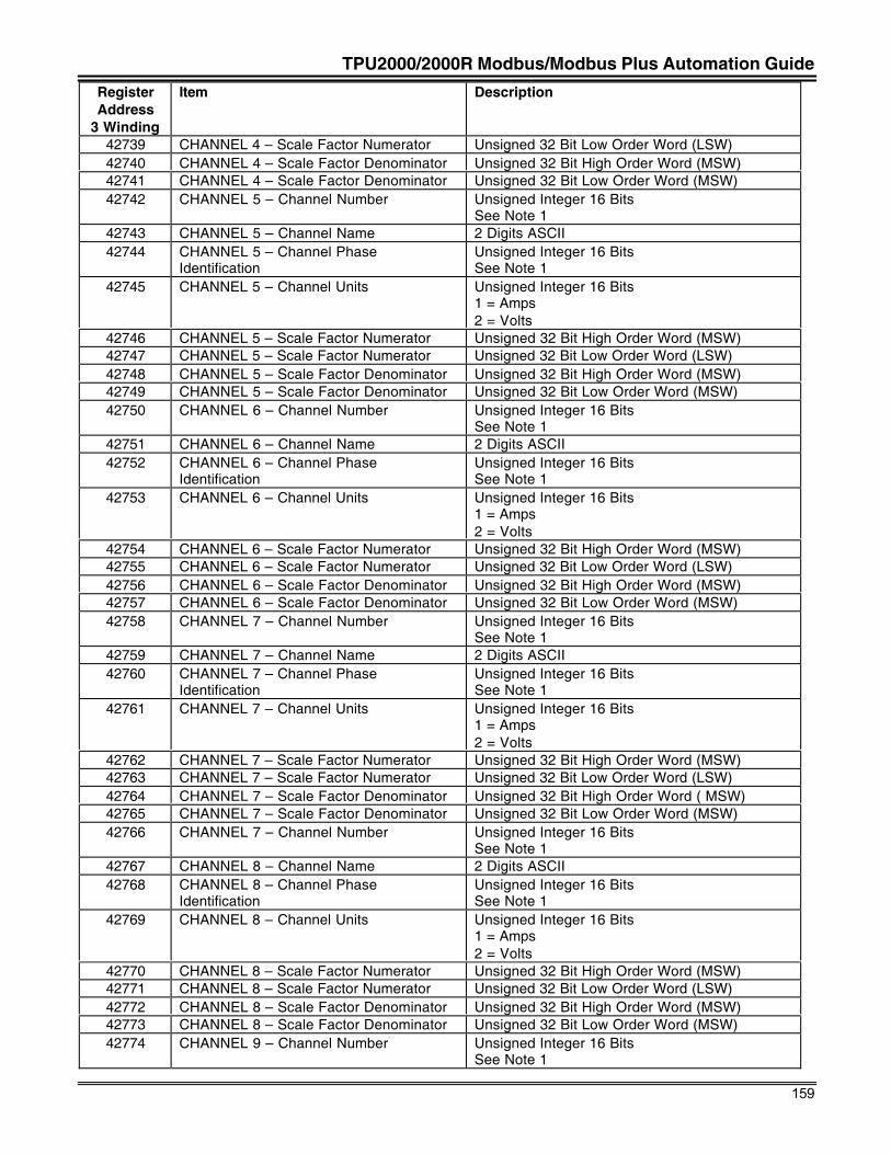
TPU2000/2000R Modbus/Modbus Plus Automation Guide
159
RegisterAddress
3 Winding
Item Description
42739 CHANNEL 4 – Scale Factor Numerator Unsigned 32 Bit Low Order Word (LSW)42740 CHANNEL 4 – Scale Factor Denominator Unsigned 32 Bit High Order Word (MSW)42741 CHANNEL 4 – Scale Factor Denominator Unsigned 32 Bit Low Order Word (MSW)42742 CHANNEL 5 – Channel Number Unsigned Integer 16 Bits
See Note 142743 CHANNEL 5 – Channel Name 2 Digits ASCII42744 CHANNEL 5 – Channel Phase
IdentificationUnsigned Integer 16 BitsSee Note 1
42745 CHANNEL 5 – Channel Units Unsigned Integer 16 Bits1 = Amps2 = Volts
42746 CHANNEL 5 – Scale Factor Numerator Unsigned 32 Bit High Order Word (MSW)42747 CHANNEL 5 – Scale Factor Numerator Unsigned 32 Bit Low Order Word (LSW)42748 CHANNEL 5 – Scale Factor Denominator Unsigned 32 Bit High Order Word (MSW)42749 CHANNEL 5 – Scale Factor Denominator Unsigned 32 Bit Low Order Word (MSW)42750 CHANNEL 6 – Channel Number Unsigned Integer 16 Bits
See Note 142751 CHANNEL 6 – Channel Name 2 Digits ASCII42752 CHANNEL 6 – Channel Phase
IdentificationUnsigned Integer 16 BitsSee Note 1
42753 CHANNEL 6 – Channel Units Unsigned Integer 16 Bits1 = Amps2 = Volts
42754 CHANNEL 6 – Scale Factor Numerator Unsigned 32 Bit High Order Word (MSW)42755 CHANNEL 6 – Scale Factor Numerator Unsigned 32 Bit Low Order Word (LSW)42756 CHANNEL 6 – Scale Factor Denominator Unsigned 32 Bit High Order Word (MSW)42757 CHANNEL 6 – Scale Factor Denominator Unsigned 32 Bit Low Order Word (MSW)42758 CHANNEL 7 – Channel Number Unsigned Integer 16 Bits
See Note 142759 CHANNEL 7 – Channel Name 2 Digits ASCII42760 CHANNEL 7 – Channel Phase
IdentificationUnsigned Integer 16 BitsSee Note 1
42761 CHANNEL 7 – Channel Units Unsigned Integer 16 Bits1 = Amps2 = Volts
42762 CHANNEL 7 – Scale Factor Numerator Unsigned 32 Bit High Order Word (MSW)42763 CHANNEL 7 – Scale Factor Numerator Unsigned 32 Bit Low Order Word (LSW)42764 CHANNEL 7 – Scale Factor Denominator Unsigned 32 Bit High Order Word ( MSW)42765 CHANNEL 7 – Scale Factor Denominator Unsigned 32 Bit Low Order Word (MSW)42766 CHANNEL 7 – Channel Number Unsigned Integer 16 Bits
See Note 142767 CHANNEL 8 – Channel Name 2 Digits ASCII42768 CHANNEL 8 – Channel Phase
IdentificationUnsigned Integer 16 BitsSee Note 1
42769 CHANNEL 8 – Channel Units Unsigned Integer 16 Bits1 = Amps2 = Volts
42770 CHANNEL 8 – Scale Factor Numerator Unsigned 32 Bit High Order Word (MSW)42771 CHANNEL 8 – Scale Factor Numerator Unsigned 32 Bit Low Order Word (LSW)42772 CHANNEL 8 – Scale Factor Denominator Unsigned 32 Bit High Order Word (MSW)42773 CHANNEL 8 – Scale Factor Denominator Unsigned 32 Bit Low Order Word (MSW)42774 CHANNEL 9 – Channel Number Unsigned Integer 16 Bits
See Note 1
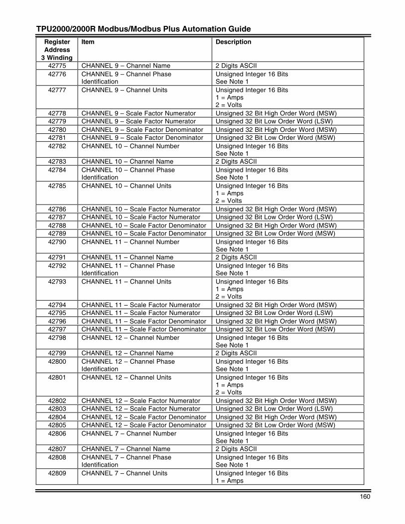
TPU2000/2000R Modbus/Modbus Plus Automation Guide
160
RegisterAddress
3 Winding
Item Description
42775 CHANNEL 9 – Channel Name 2 Digits ASCII42776 CHANNEL 9 – Channel Phase
IdentificationUnsigned Integer 16 BitsSee Note 1
42777 CHANNEL 9 – Channel Units Unsigned Integer 16 Bits1 = Amps2 = Volts
42778 CHANNEL 9 – Scale Factor Numerator Unsigned 32 Bit High Order Word (MSW)42779 CHANNEL 9 – Scale Factor Numerator Unsigned 32 Bit Low Order Word (LSW)42780 CHANNEL 9 – Scale Factor Denominator Unsigned 32 Bit High Order Word (MSW)42781 CHANNEL 9 – Scale Factor Denominator Unsigned 32 Bit Low Order Word (MSW)42782 CHANNEL 10 – Channel Number Unsigned Integer 16 Bits
See Note 142783 CHANNEL 10 – Channel Name 2 Digits ASCII42784 CHANNEL 10 – Channel Phase
IdentificationUnsigned Integer 16 BitsSee Note 1
42785 CHANNEL 10 – Channel Units Unsigned Integer 16 Bits1 = Amps2 = Volts
42786 CHANNEL 10 – Scale Factor Numerator Unsigned 32 Bit High Order Word (MSW)42787 CHANNEL 10 – Scale Factor Numerator Unsigned 32 Bit Low Order Word (LSW)42788 CHANNEL 10 – Scale Factor Denominator Unsigned 32 Bit High Order Word (MSW)42789 CHANNEL 10 – Scale Factor Denominator Unsigned 32 Bit Low Order Word (MSW)42790 CHANNEL 11 – Channel Number Unsigned Integer 16 Bits
See Note 142791 CHANNEL 11 – Channel Name 2 Digits ASCII42792 CHANNEL 11 – Channel Phase
IdentificationUnsigned Integer 16 BitsSee Note 1
42793 CHANNEL 11 – Channel Units Unsigned Integer 16 Bits1 = Amps2 = Volts
42794 CHANNEL 11 – Scale Factor Numerator Unsigned 32 Bit High Order Word (MSW)42795 CHANNEL 11 – Scale Factor Numerator Unsigned 32 Bit Low Order Word (LSW)42796 CHANNEL 11 – Scale Factor Denominator Unsigned 32 Bit High Order Word (MSW)42797 CHANNEL 11 – Scale Factor Denominator Unsigned 32 Bit Low Order Word (MSW)42798 CHANNEL 12 – Channel Number Unsigned Integer 16 Bits
See Note 142799 CHANNEL 12 – Channel Name 2 Digits ASCII42800 CHANNEL 12 – Channel Phase
IdentificationUnsigned Integer 16 BitsSee Note 1
42801 CHANNEL 12 – Channel Units Unsigned Integer 16 Bits1 = Amps2 = Volts
42802 CHANNEL 12 – Scale Factor Numerator Unsigned 32 Bit High Order Word (MSW)42803 CHANNEL 12 – Scale Factor Numerator Unsigned 32 Bit Low Order Word (LSW)42804 CHANNEL 12 – Scale Factor Denominator Unsigned 32 Bit High Order Word (MSW)42805 CHANNEL 12 – Scale Factor Denominator Unsigned 32 Bit Low Order Word (MSW)42806 CHANNEL 7 – Channel Number Unsigned Integer 16 Bits
See Note 142807 CHANNEL 7 – Channel Name 2 Digits ASCII42808 CHANNEL 7 – Channel Phase
IdentificationUnsigned Integer 16 BitsSee Note 1
42809 CHANNEL 7 – Channel Units Unsigned Integer 16 Bits1 = Amps
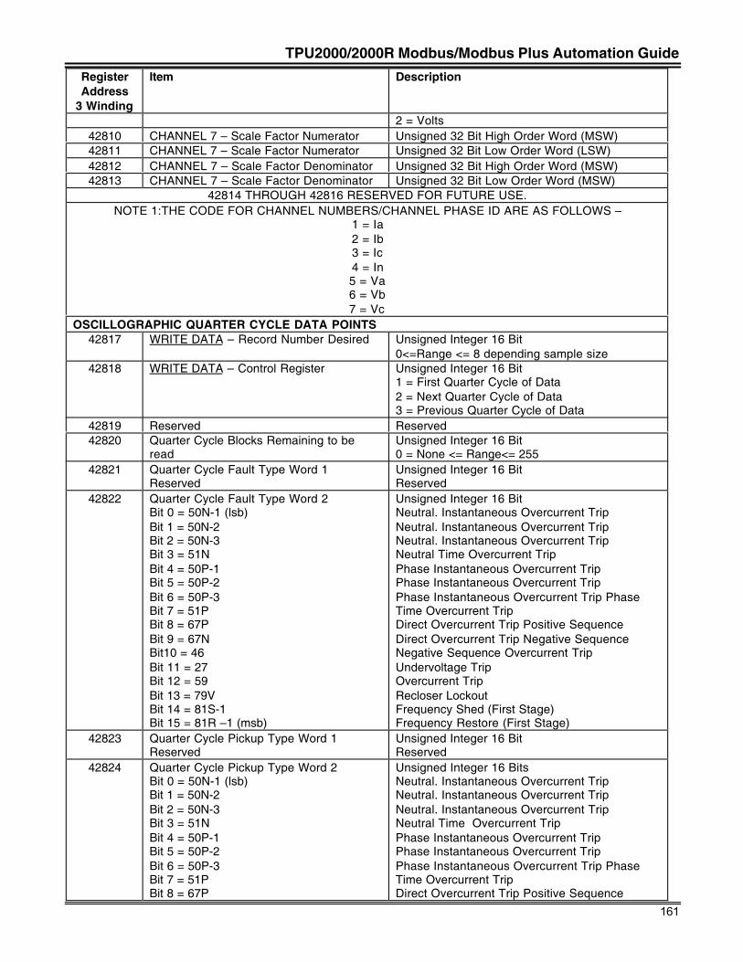
TPU2000/2000R Modbus/Modbus Plus Automation Guide
161
RegisterAddress
3 Winding
Item Description
2 = Volts42810 CHANNEL 7 – Scale Factor Numerator Unsigned 32 Bit High Order Word (MSW)42811 CHANNEL 7 – Scale Factor Numerator Unsigned 32 Bit Low Order Word (LSW)42812 CHANNEL 7 – Scale Factor Denominator Unsigned 32 Bit High Order Word (MSW)42813 CHANNEL 7 – Scale Factor Denominator Unsigned 32 Bit Low Order Word (MSW)
42814 THROUGH 42816 RESERVED FOR FUTURE USE.NOTE 1:THE CODE FOR CHANNEL NUMBERS/CHANNEL PHASE ID ARE AS FOLLOWS –
1 = Ia2 = Ib3 = Ic4 = In5 = Va6 = Vb7 = Vc
OSCILLOGRAPHIC QUARTER CYCLE DATA POINTS42817 WRITE DATA – Record Number Desired Unsigned Integer 16 Bit
0<=Range <= 8 depending sample size42818 WRITE DATA – Control Register Unsigned Integer 16 Bit
1 = First Quarter Cycle of Data2 = Next Quarter Cycle of Data3 = Previous Quarter Cycle of Data
42819 Reserved Reserved42820 Quarter Cycle Blocks Remaining to be
readUnsigned Integer 16 Bit0 = None <= Range<= 255
42821 Quarter Cycle Fault Type Word 1Reserved
Unsigned Integer 16 BitReserved
42822 Quarter Cycle Fault Type Word 2Bit 0 = 50N-1 (lsb)Bit 1 = 50N-2Bit 2 = 50N-3Bit 3 = 51NBit 4 = 50P-1Bit 5 = 50P-2Bit 6 = 50P-3Bit 7 = 51PBit 8 = 67PBit 9 = 67NBit10 = 46Bit 11 = 27Bit 12 = 59Bit 13 = 79VBit 14 = 81S-1Bit 15 = 81R –1 (msb)
Unsigned Integer 16 BitNeutral. Instantaneous Overcurrent TripNeutral. Instantaneous Overcurrent TripNeutral. Instantaneous Overcurrent TripNeutral Time Overcurrent TripPhase Instantaneous Overcurrent TripPhase Instantaneous Overcurrent TripPhase Instantaneous Overcurrent Trip PhaseTime Overcurrent TripDirect Overcurrent Trip Positive SequenceDirect Overcurrent Trip Negative SequenceNegative Sequence Overcurrent TripUndervoltage TripOvercurrent TripRecloser LockoutFrequency Shed (First Stage)Frequency Restore (First Stage)
42823 Quarter Cycle Pickup Type Word 1Reserved
Unsigned Integer 16 BitReserved
42824 Quarter Cycle Pickup Type Word 2Bit 0 = 50N-1 (lsb)Bit 1 = 50N-2Bit 2 = 50N-3Bit 3 = 51NBit 4 = 50P-1Bit 5 = 50P-2Bit 6 = 50P-3Bit 7 = 51PBit 8 = 67P
Unsigned Integer 16 BitsNeutral. Instantaneous Overcurrent TripNeutral. Instantaneous Overcurrent TripNeutral. Instantaneous Overcurrent TripNeutral Time Overcurrent TripPhase Instantaneous Overcurrent TripPhase Instantaneous Overcurrent TripPhase Instantaneous Overcurrent Trip PhaseTime Overcurrent TripDirect Overcurrent Trip Positive Sequence
TPU2000/2000R Modbus/Modbus Plus Automation Guide
162
RegisterAddress
3 Winding
Item Description
Bit 9 = 67NBit10 = 46Bit 11 = 27Bit 12 = 59Bit 13 = 79VBit 14 = 81S-1Bit 15 = 81R –1 (msb)
Direct Overcurrent Trip Negative SequenceNegative Sequence Overcurrent TripUndervoltage TripOvercurrent TripRecloser LockoutFrequency Shed (First Stage)Frequency Restore (First Stage)
42825 Quarter Cycle Miscellaneous Data Word 1Reserved
Unsigned Integer 16 BitsReserved
42826 Quarter Cycle Miscellaneous Data Word 2Bit 0 = Master Trip(lsb)Bit 1 = 52 aBit 2 = BFABit 3 = ReservedBit 4 = ReservedBit 5 = ReservedBit 6 = ReservedBit 7 = ReservedBit 8 = ReservedBit 9 = ReservedBit10 = ReservedBit 11 = ReservedBit 12 = ReservedBit 13 = ReservedBit 14 = ReservedBit 15 = Reserved (msb)
Unsigned Integer 16 BitsMaster Trip StatusBreaker Status (1 = Open, 0 = Closed)Breaker Fail AlarmReservedReservedReservedReservedReservedReservedReservedReservedReservedReservedReservedReservedReserved
OSCILLOGRAPHIC DATA POINTS42827 CHANNEL 1 POINT 1 Signed Integer 16 Bits42828 CHANNEL 2 POINT 1 Signed Integer 16 Bits42829 CHANNEL 3 POINT 1 Signed Integer 16 Bits42830 CHANNEL 4 POINT 1 Signed Integer 16 Bits42831 CHANNEL 5 POINT 1 Signed Integer 16 Bits42832 CHANNEL 6 POINT 1 Signed Integer 16 Bits42833 CHANNEL 7 POINT 1 Signed Integer 16 Bits42834 CHANNEL 1 POINT 2 Signed Integer 16 Bits42835 CHANNEL 2 POINT 2 Signed Integer 16 Bits42836 CHANNEL 3 POINT 2 Signed Integer 16 Bits42837 CHANNEL 4 POINT 2 Signed Integer 16 Bits42838 CHANNEL 5 POINT 2 Signed Integer 16 Bits42839 CHANNEL 6 POINT 2 Signed Integer 16 Bits42840 CHANNEL 7 POINT 2 Signed Integer 16 Bits42841 CHANNEL 1 POINT 3 Signed Integer 16 Bits42842 CHANNEL 2 POINT 3 Signed Integer 16 Bits42843 CHANNEL 3 POINT 3 Signed Integer 16 Bits42844 CHANNEL 4 POINT 3 Signed Integer 16 Bits42845 CHANNEL 5 POINT 3 Signed Integer 16 Bits42846 CHANNEL 6 POINT 3 Signed Integer 16 Bits42847 CHANNEL 7 POINT 3 Signed Integer 16 Bits42848 CHANNEL 1 POINT 4 Signed Integer 16 Bits42849 CHANNEL 2 POINT 4 Signed Integer 16 Bits42850 CHANNEL 3 POINT 4 Signed Integer 16 Bits42851 CHANNEL 4 POINT 4 Signed Integer 16 Bits42852 CHANNEL 5 POINT 4 Signed Integer 16 Bits
TPU2000/2000R Modbus/Modbus Plus Automation Guide
163
RegisterAddress
3 Winding
Item Description
42853 CHANNEL 6 POINT 4 Signed Integer 16 Bits42854 CHANNEL 7 POINT 4 Signed Integer 16 Bits42855 CHANNEL 1 POINT 5 Signed Integer 16 Bits42856 CHANNEL 2 POINT 5 Signed Integer 16 Bits42857 CHANNEL 3 POINT 5 Signed Integer 16 Bits42858 CHANNEL 4 POINT 5 Signed Integer 16 Bits42859 CHANNEL 5 POINT 5 Signed Integer 16 Bits42860 CHANNEL 6 POINT 5 Signed Integer 16 Bits42861 CHANNEL 7 POINT 5 Signed Integer 16 Bits42862 CHANNEL 1 POINT 6 Signed Integer 16 Bits42863 CHANNEL 2 POINT 6 Signed Integer 16 Bits42864 CHANNEL 3 POINT 6 Signed Integer 16 Bits42865 CHANNEL 4 POINT 6 Signed Integer 16 Bits42866 CHANNEL 5 POINT 6 Signed Integer 16 Bits42867 CHANNEL 6 POINT 6 Signed Integer 16 Bits42868 CHANNEL 7 POINT 6 Signed Integer 16 Bits42869 CHANNEL 1 POINT 7 Signed Integer 16 Bits42870 CHANNEL 2 POINT 7 Signed Integer 16 Bits42871 CHANNEL 3 POINT 7 Signed Integer 16 Bits42872 CHANNEL 4 POINT 7 Signed Integer 16 Bits42873 CHANNEL 5 POINT 7 Signed Integer 16 Bits42874 CHANNEL 6 POINT 7 Signed Integer 16 Bits42875 CHANNEL 7 POINT 7 Signed Integer 16 Bits42876 CHANNEL 1 POINT 8 Signed Integer 16 Bits42877 CHANNEL 2 POINT 8 Signed Integer 16 Bits42878 CHANNEL 3 POINT 8 Signed Integer 16 Bits42879 CHANNEL 4 POINT 8 Signed Integer 16 Bits42880 CHANNEL 5 POINT 8 Signed Integer 16 Bits42881 CHANNEL 6 POINT 8 Signed Integer 16 Bits42882 CHANNEL 7 POINT 8 Signed Integer 16 Bits42883 CHANNEL 1 POINT 9 Signed Integer 16 Bits42884 CHANNEL 2 POINT 9 Signed Integer 16 Bits42885 CHANNEL 3 POINT 9 Signed Integer 16 Bits42886 CHANNEL 4 POINT 9 Signed Integer 16 Bits42887 CHANNEL 5 POINT 9 Signed Integer 16 Bits42888 CHANNEL 6 POINT 9 Signed Integer 16 Bits42889 CHANNEL 7 POINT 9 Signed Integer 16 Bits42890 CHANNEL 1 POINT 10 Signed Integer 16 Bits42891 CHANNEL 2 POINT 10 Signed Integer 16 Bits42892 CHANNEL 3 POINT 10 Signed Integer 16 Bits42893 CHANNEL 4 POINT 10 Signed Integer 16 Bits42894 CHANNEL 5 POINT 10 Signed Integer 16 Bits42895 CHANNEL 6 POINT 10 Signed Integer 16 Bits42896 CHANNEL 7 POINT 10 Signed Integer 16 Bits4289742898428994290042901429024290342904
TPU2000/2000R Modbus/Modbus Plus Automation Guide
164
RegisterAddress
3 Winding
Item Description
42905429064290742908429094291042911429124291342914429154291642917429184291942920429214292242923429244292542926429274292842929429304293142932429334293442935429364293742938
Oscillographic Data Interpretation
Once the point and configuration data is obtained from the relay, constructing the waveform curve is fairlystraightforward as illustrated in Figure 5-63. The mathematics required for obtaining point data follows:
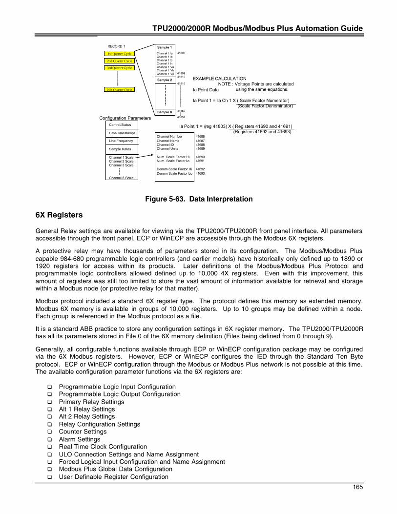
TPU2000/2000R Modbus/Modbus Plus Automation Guide
165
1st Quarter Cycle
2nd Quarter Cycle
3rd Quarter Cycle
Nth Quarter Cycle
RECORD 1
Channel 1 IaChannel 1 IbChannel 1 IcChannel 1 InChannel 1 VaChannel 1 VbChannel 1 Vc
Sample 2
Sample 1
Sample 8
41803
4180941810
41816
41850
41857
EXAMPLE CALCULATION
Ia Point Data
Ia Point 1 = Ia Ch 1 X ( Scale Factor Numerator) (Scale Factor Denominator)
Ia Point 1 = (reg 41803) X ( Registers 41690 and 41691) (Registers 41692 and 41693)
Configuration Parameters
NOTE : Voltage Points are calculated using the same equations.
Control/Status
Date/Timestamps
Line Frequency
Sample Rates
Channel 1 ScaleChannel 2 ScaleChannel 3 Scale
Channel 8 Scale
Channel NumberChannel NameChannel IDChannel Units
Num. Scale Factor HiNum. Scale Factor Lo
Denom Scale Factor HiDenom Scale Factor Lo
41686416874168841689
4169041691
4169241693
Figure 5-63. Data Interpretation
6X Registers
General Relay settings are available for viewing via the TPU2000/TPU2000R front panel interface. All parametersaccessible through the front panel, ECP or WinECP are accessible through the Modbus 6X registers.
A protective relay may have thousands of parameters stored in its configuration. The Modbus/Modbus Pluscapable 984-680 programmable logic controllers (and earlier models) have historically only defined up to 1890 or1920 registers for access within its products. Later definitions of the Modbus/Modbus Plus Protocol andprogrammable logic controllers allowed defined up to 10,000 4X registers. Even with this improvement, thisamount of registers was still too limited to store the vast amount of information available for retrieval and storagewithin a Modbus node (or protective relay for that matter).
Modbus protocol included a standard 6X register type. The protocol defines this memory as extended memory.Modbus 6X memory is available in groups of 10,000 registers. Up to 10 groups may be defined within a node.Each group is referenced in the Modbus protocol as a file.
It is a standard ABB practice to store any configuration settings in 6X register memory. The TPU2000/TPU2000Rhas all its parameters stored in File 0 of the 6X memory definition (Files being defined from 0 through 9).
Generally, all configurable functions available through ECP or WinECP configuration package may be configuredvia the 6X Modbus registers. However, ECP or WinECP configures the IED through the Standard Ten Byteprotocol. ECP or WinECP configuration through the Modbus or Modbus Plus network is not possible at this time.The available configuration parameter functions via the 6X registers are:
q Programmable Logic Input Configurationq Programmable Logic Output Configurationq Primary Relay Settingsq Alt 1 Relay Settingsq Alt 2 Relay Settingsq Relay Configuration Settingsq Counter Settingsq Alarm Settingsq Real Time Clock Configurationq ULO Connection Settings and Name Assignmentq Forced Logical Input Configuration and Name Assignmentq Modbus Plus Global Data Configurationq User Definable Register Configuration
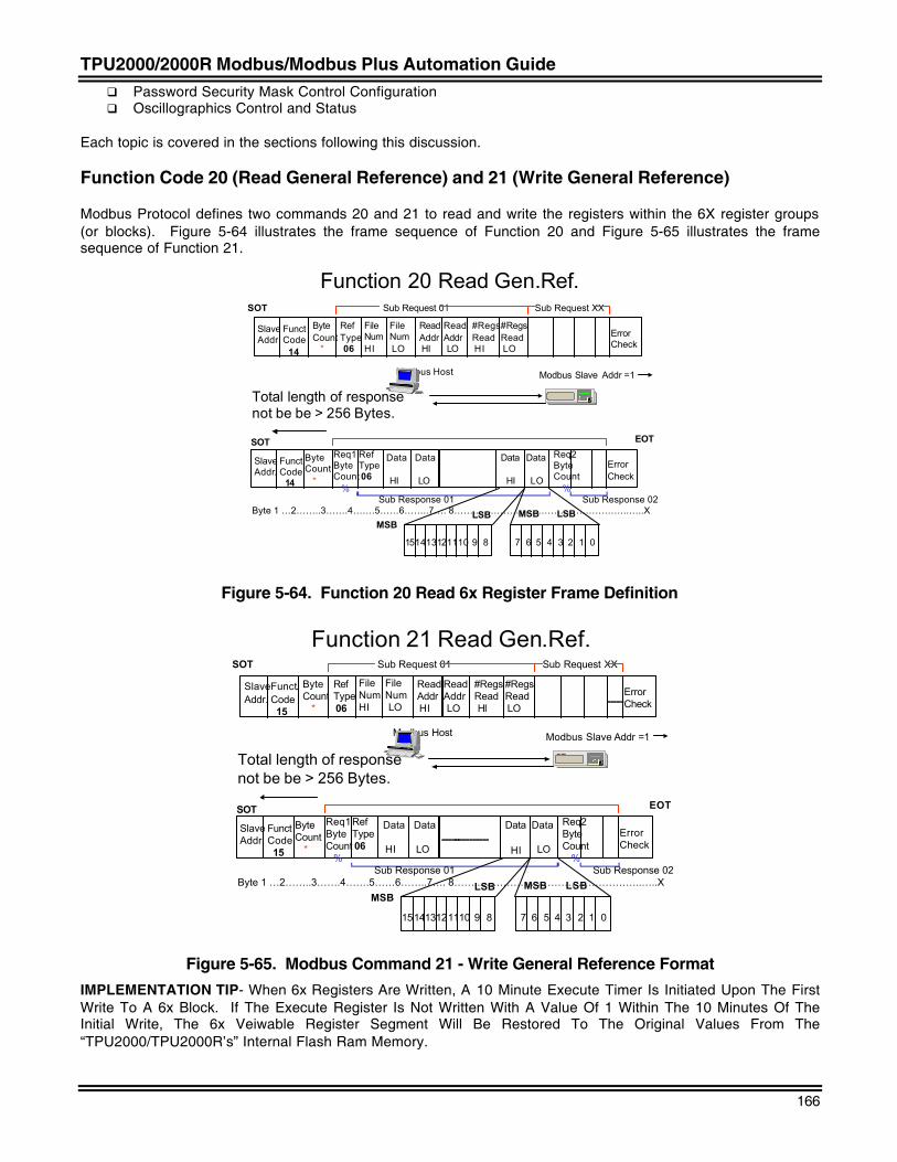
TPU2000/2000R Modbus/Modbus Plus Automation Guide
166
q Password Security Mask Control Configurationq Oscillographics Control and Status
Each topic is covered in the sections following this discussion.
Function Code 20 (Read General Reference) and 21 (Write General Reference)
Modbus Protocol defines two commands 20 and 21 to read and write the registers within the 6X register groups(or blocks). Figure 5-64 illustrates the frame sequence of Function 20 and Figure 5-65 illustrates the framesequence of Function 21.
Function 20 Read Gen.Ref.
Modbus Host
SlaveAddr.
Funct .Code 14
ErrorCheck
ReadAddr HI
ReadAddr LO
#RegsRead HI
#RegsRead LO
ByteCount *
RefType 06
FileNumHI
FileNum LO
Sub Request 01 Sub Request XX
EC
Modbus Slave Addr =1
SOT
SlaveAddr.
Funct.Code 14
Data
LO
Data
HI
Byte 1 …2……..3…….4…….5……6……..7…. 8……...………………………………………..…..X
Data
HI
Data
LO
ErrorCheck
ByteCount *
Req1ByteCount %
RefType 06
Sub Response 01 Sub Response 02
SOT EOT
Total length of responsenot be be > 256 Bytes.
Req2ByteCount %
MSBLSB
151413121110 9 8 7 6 5 4 3 2 1 0
MSB LSB
Figure 5-64. Function 20 Read 6x Register Frame Definition
Function 21 Read Gen.Ref.
Modbus Host
SlaveAddr.
Funct.Code 15
ErrorCheck
ReadAddr HI
ReadAddr LO
#RegsRead HI
#RegsRead LO
ByteCount *
RefType 06
FileNumHI
FileNum LO
Sub Request 01 Sub Request XX
EC
Modbus Slave Addr =1
SOT
SlaveAddr.
Funct.Code 15
Data
LO
Data
HI
Byte 1 …2……..3…….4…….5……6……..7…. 8……...………………………………………..…..X
Data
HI
Data
LO
ErrorCheck
ByteCount *
Req1ByteCount %
RefType 06
Sub Response 01 Sub Response 02
SOT EOT
Total length of responsenot be be > 256 Bytes.
Req2ByteCount %
MSBLSB
151413121110 9 8 7 6 5 4 3 2 1 0
MSB LSB
Figure 5-65. Modbus Command 21 - Write General Reference FormatIMPLEMENTATION TIP- When 6x Registers Are Written, A 10 Minute Execute Timer Is Initiated Upon The FirstWrite To A 6x Block. If The Execute Register Is Not Written With A Value Of 1 Within The 10 Minutes Of TheInitial Write, The 6x Veiwable Register Segment Will Be Restored To The Original Values From The“TPU2000/TPU2000R’s” Internal Flash Ram Memory.
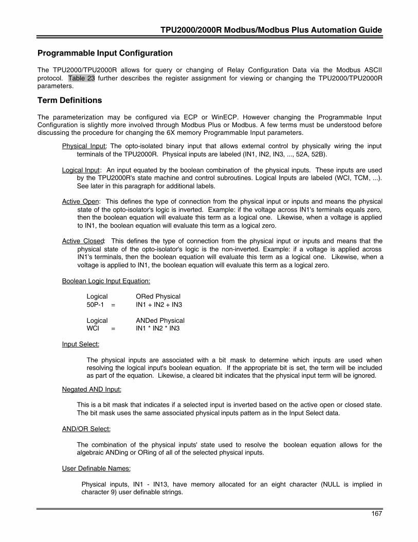
TPU2000/2000R Modbus/Modbus Plus Automation Guide
167
Programmable Input Configuration
The TPU2000/TPU2000R allows for query or changing of Relay Configuration Data via the Modbus ASCIIprotocol. Table 23 further describes the register assignment for viewing or changing the TPU2000/TPU2000Rparameters.
Term Definitions
The parameterization may be configured via ECP or WinECP. However changing the Programmable InputConfiguration is slightly more involved through Modbus Plus or Modbus. A few terms must be understood beforediscussing the procedure for changing the 6X memory Programmable Input parameters.
Physical Input: The opto-isolated binary input that allows external control by physically wiring the inputterminals of the TPU2000R. Physical inputs are labeled (IN1, IN2, IN3, ..., 52A, 52B).
Logical Input: An input equated by the boolean combination of the physical inputs. These inputs are usedby the TPU2000R's state machine and control subroutines. Logical Inputs are labeled (WCI, TCM, ...).See later in this paragraph for additional labels.
Active Open: This defines the type of connection from the physical input or inputs and means the physicalstate of the opto-isolator's logic is inverted. Example: if the voltage across IN1's terminals equals zero,then the boolean equation will evaluate this term as a logical one. Likewise, when a voltage is appliedto IN1, the boolean equation will evaluate this term as a logical zero.
Active Closed: This defines the type of connection from the physical input or inputs and means that thephysical state of the opto-isolator's logic is the non-inverted. Example: if a voltage is applied acrossIN1's terminals, then the boolean equation will evaluate this term as a logical one. Likewise, when avoltage is applied to IN1, the boolean equation will evaluate this term as a logical zero.
Boolean Logic Input Equation:
Logical ORed Physical50P-1 = IN1 + IN2 + IN3
Logical ANDed PhysicalWCI = IN1 * IN2 * IN3
Input Select:
The physical inputs are associated with a bit mask to determine which inputs are used whenresolving the logical input's boolean equation. If the appropriate bit is set, the term will be includedas part of the equation. Likewise, a cleared bit indicates that the physical input term will be ignored.
Negated AND Input:
This is a bit mask that indicates if a selected input is inverted based on the active open or closed state.The bit mask uses the same associated physical inputs pattern as in the Input Select data.
AND/OR Select:
The combination of the physical inputs' state used to resolve the boolean equation allows for thealgebraic ANDing or ORing of all of the selected physical inputs.
User Definable Names:
Physical inputs, IN1 - IN13, have memory allocated for an eight character (NULL is implied incharacter 9) user definable strings.
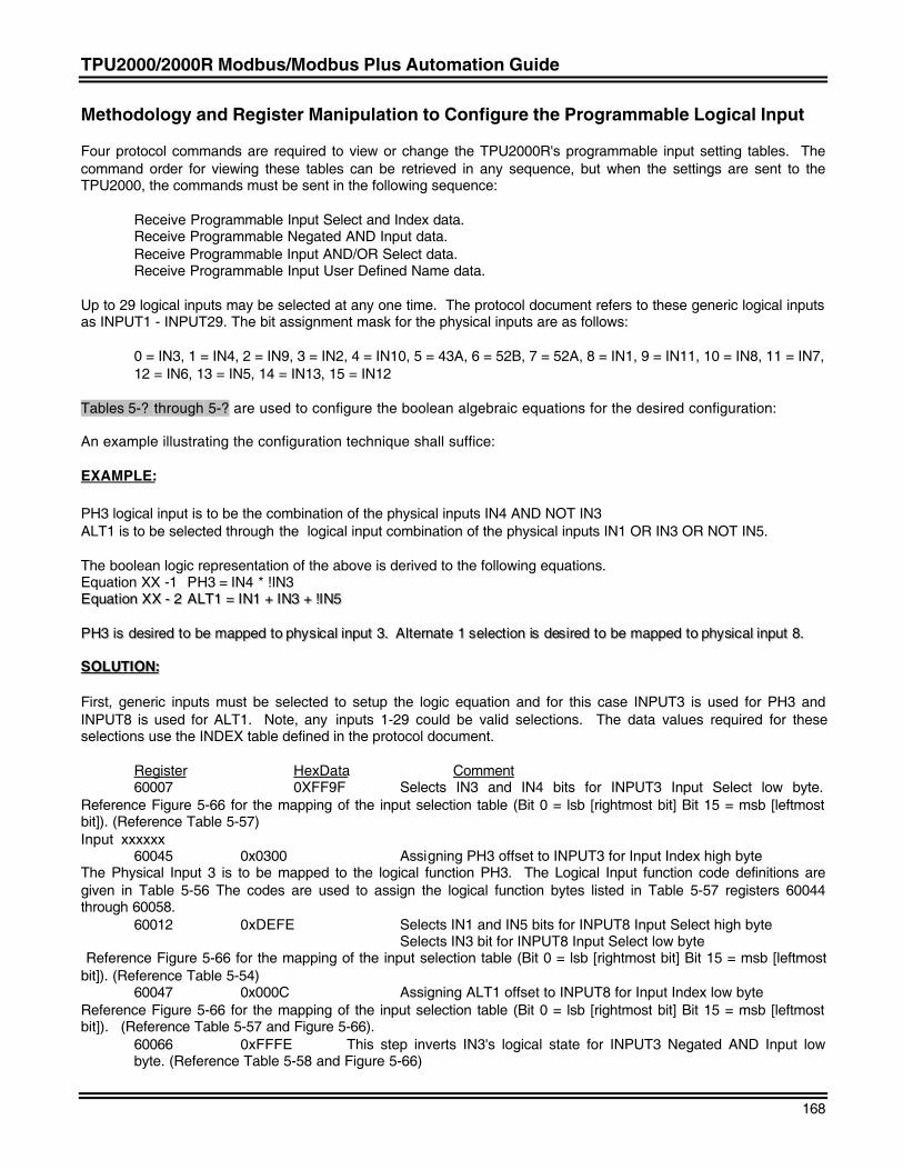
TPU2000/2000R Modbus/Modbus Plus Automation Guide
168
Methodology and Register Manipulation to Configure the Programmable Logical Input
Four protocol commands are required to view or change the TPU2000R's programmable input setting tables. Thecommand order for viewing these tables can be retrieved in any sequence, but when the settings are sent to theTPU2000, the commands must be sent in the following sequence:
Receive Programmable Input Select and Index data.Receive Programmable Negated AND Input data.Receive Programmable Input AND/OR Select data.Receive Programmable Input User Defined Name data.
Up to 29 logical inputs may be selected at any one time. The protocol document refers to these generic logical inputsas INPUT1 - INPUT29. The bit assignment mask for the physical inputs are as follows:
0 = IN3, 1 = IN4, 2 = IN9, 3 = IN2, 4 = IN10, 5 = 43A, 6 = 52B, 7 = 52A, 8 = IN1, 9 = IN11, 10 = IN8, 11 = IN7,12 = IN6, 13 = IN5, 14 = IN13, 15 = IN12
Tables 5-? through 5-? are used to configure the boolean algebraic equations for the desired configuration:
An example illustrating the configuration technique shall suffice:
EXAMPLE:
PH3 logical input is to be the combination of the physical inputs IN4 AND NOT IN3ALT1 is to be selected through the logical input combination of the physical inputs IN1 OR IN3 OR NOT IN5.
The boolean logic representation of the above is derived to the following equations.Equation XX -1 PH3 = IN4 * !IN3EEqquuaatt iioonn XXXX -- 22 AALLTT11 == IINN11 ++ IINN33 ++ !!IINN55
PPHH33 iiss ddeessiirreedd ttoo bbee mmaappppeedd ttoo pphhyyss iiccaall iinnppuutt 33.. AAlltteerrnnaattee 11 sseelleecctt iioonn iiss ddeess iirreedd ttoo bbee mmaappppeedd ttoo pphhyyssiiccaall iinnppuutt 88..
SSOOLLUUTTIIOONN::
First, generic inputs must be selected to setup the logic equation and for this case INPUT3 is used for PH3 andINPUT8 is used for ALT1. Note, any inputs 1-29 could be valid selections. The data values required for theseselections use the INDEX table defined in the protocol document.
Register HexData Comment60007 0XFF9F Selects IN3 and IN4 bits for INPUT3 Input Select low byte.
Reference Figure 5-66 for the mapping of the input selection table (Bit 0 = lsb [rightmost bit] Bit 15 = msb [leftmostbit]). (Reference Table 5-57)Input xxxxxx
60045 0x0300 Assigning PH3 offset to INPUT3 for Input Index high byteThe Physical Input 3 is to be mapped to the logical function PH3. The Logical Input function code definitions aregiven in Table 5-56 The codes are used to assign the logical function bytes listed in Table 5-57 registers 60044through 60058.
60012 0xDEFE Selects IN1 and IN5 bits for INPUT8 Input Select high byte Selects IN3 bit for INPUT8 Input Select low byte
Reference Figure 5-66 for the mapping of the input selection table (Bit 0 = lsb [rightmost bit] Bit 15 = msb [leftmostbit]). (Reference Table 5-54)
60047 0x000C Assigning ALT1 offset to INPUT8 for Input Index low byteReference Figure 5-66 for the mapping of the input selection table (Bit 0 = lsb [rightmost bit] Bit 15 = msb [leftmostbit]). (Reference Table 5-57 and Figure 5-66).
60066 0xFFFE This step inverts IN3's logical state for INPUT3 Negated AND Input lowbyte. (Reference Table 5-58 and Figure 5-66)
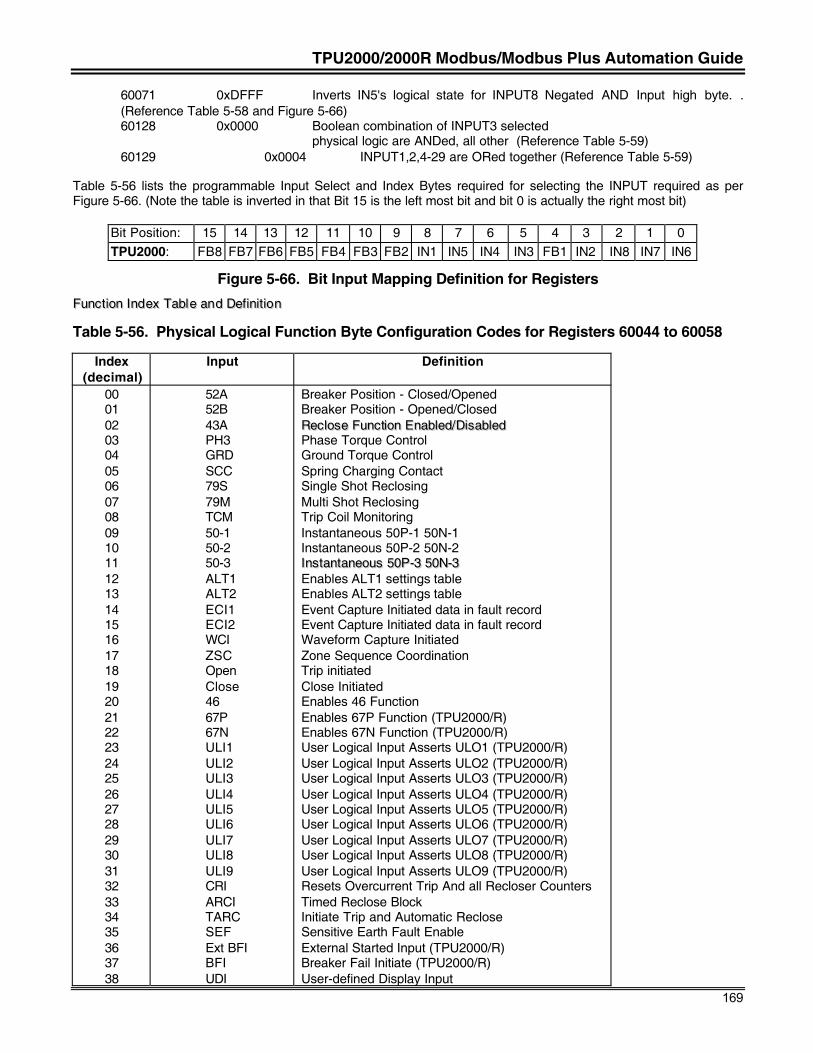
TPU2000/2000R Modbus/Modbus Plus Automation Guide
169
60071 0xDFFF Inverts IN5's logical state for INPUT8 Negated AND Input high byte. .(Reference Table 5-58 and Figure 5-66)60128 0x0000 Boolean combination of INPUT3 selected
physical logic are ANDed, all other (Reference Table 5-59)60129 0x0004 INPUT1,2,4-29 are ORed together (Reference Table 5-59)
Table 5-56 lists the programmable Input Select and Index Bytes required for selecting the INPUT required as perFigure 5-66. (Note the table is inverted in that Bit 15 is the left most bit and bit 0 is actually the right most bit)
Bit Position: 15 14 13 12 11 10 9 8 7 6 5 4 3 2 1 0TPU2000: FB8 FB7 FB6 FB5 FB4 FB3 FB2 IN1 IN5 IN4 IN3 FB1 IN2 IN8 IN7 IN6
Figure 5-66. Bit Input Mapping Definition for Registers
FFuunncctt iioonn IInnddeexx TTaabbll ee aanndd DDeeff iinnii tt iioonn
Table 5-56. Physical Logical Function Byte Configuration Codes for Registers 60044 to 60058
Index(decimal)
Input Definition
000102030405060708091011121314151617181920212223242526272829303132333435363738
52A52B43APH3GRDSCC79S79MTCM50-150-250-3ALT1ALT2ECI1ECI2WCIZSCOpenClose4667P67NULI1ULI2ULI3ULI4ULI5ULI6ULI7ULI8ULI9CRIARCITARCSEFExt BFIBFIUDI
Breaker Position - Closed/OpenedBreaker Position - Opened/ClosedRReecc lloossee FFuunnccttiioonn EEnnaabblleedd//DDiissaabblleeddPhase Torque ControlGround Torque ControlSpring Charging ContactSingle Shot ReclosingMulti Shot ReclosingTrip Coil MonitoringInstantaneous 50P-1 50N-1Instantaneous 50P-2 50N-2IInnssttaannttaanneeoouuss 5500PP--33 5500NN--33Enables ALT1 settings tableEnables ALT2 settings tableEvent Capture Initiated data in fault recordEvent Capture Initiated data in fault recordWaveform Capture InitiatedZone Sequence CoordinationTrip initiatedClose InitiatedEnables 46 FunctionEnables 67P Function (TPU2000/R)Enables 67N Function (TPU2000/R)User Logical Input Asserts ULO1 (TPU2000/R)User Logical Input Asserts ULO2 (TPU2000/R)User Logical Input Asserts ULO3 (TPU2000/R)User Logical Input Asserts ULO4 (TPU2000/R)User Logical Input Asserts ULO5 (TPU2000/R)User Logical Input Asserts ULO6 (TPU2000/R)User Logical Input Asserts ULO7 (TPU2000/R)User Logical Input Asserts ULO8 (TPU2000/R)User Logical Input Asserts ULO9 (TPU2000/R)Resets Overcurrent Trip And all Recloser CountersTimed Reclose BlockInitiate Trip and Automatic RecloseSensitive Earth Fault EnableExternal Started Input (TPU2000/R)Breaker Fail Initiate (TPU2000/R)User-defined Display Input
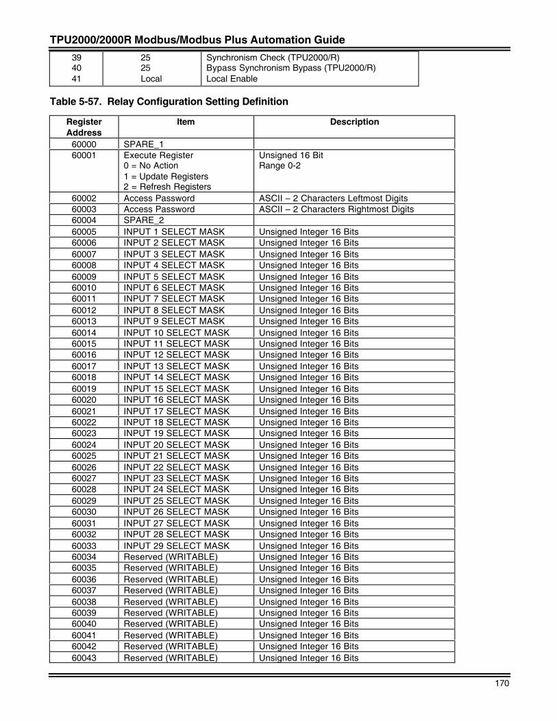
TPU2000/2000R Modbus/Modbus Plus Automation Guide
170
394041
2525Local
Synchronism Check (TPU2000/R)Bypass Synchronism Bypass (TPU2000/R)Local Enable
Table 5-57. Relay Configuration Setting Definition
RegisterAddress
Item Description
60000 SPARE_160001 Execute Register
0 = No Action1 = Update Registers2 = Refresh Registers
Unsigned 16 BitRange 0-2
60002 Access Password ASCII – 2 Characters Leftmost Digits60003 Access Password ASCII – 2 Characters Rightmost Digits60004 SPARE_260005 INPUT 1 SELECT MASK Unsigned Integer 16 Bits60006 INPUT 2 SELECT MASK Unsigned Integer 16 Bits60007 INPUT 3 SELECT MASK Unsigned Integer 16 Bits60008 INPUT 4 SELECT MASK Unsigned Integer 16 Bits60009 INPUT 5 SELECT MASK Unsigned Integer 16 Bits60010 INPUT 6 SELECT MASK Unsigned Integer 16 Bits60011 INPUT 7 SELECT MASK Unsigned Integer 16 Bits60012 INPUT 8 SELECT MASK Unsigned Integer 16 Bits60013 INPUT 9 SELECT MASK Unsigned Integer 16 Bits60014 INPUT 10 SELECT MASK Unsigned Integer 16 Bits60015 INPUT 11 SELECT MASK Unsigned Integer 16 Bits60016 INPUT 12 SELECT MASK Unsigned Integer 16 Bits60017 INPUT 13 SELECT MASK Unsigned Integer 16 Bits60018 INPUT 14 SELECT MASK Unsigned Integer 16 Bits60019 INPUT 15 SELECT MASK Unsigned Integer 16 Bits60020 INPUT 16 SELECT MASK Unsigned Integer 16 Bits60021 INPUT 17 SELECT MASK Unsigned Integer 16 Bits60022 INPUT 18 SELECT MASK Unsigned Integer 16 Bits60023 INPUT 19 SELECT MASK Unsigned Integer 16 Bits60024 INPUT 20 SELECT MASK Unsigned Integer 16 Bits60025 INPUT 21 SELECT MASK Unsigned Integer 16 Bits60026 INPUT 22 SELECT MASK Unsigned Integer 16 Bits60027 INPUT 23 SELECT MASK Unsigned Integer 16 Bits60028 INPUT 24 SELECT MASK Unsigned Integer 16 Bits60029 INPUT 25 SELECT MASK Unsigned Integer 16 Bits60030 INPUT 26 SELECT MASK Unsigned Integer 16 Bits60031 INPUT 27 SELECT MASK Unsigned Integer 16 Bits60032 INPUT 28 SELECT MASK Unsigned Integer 16 Bits60033 INPUT 29 SELECT MASK Unsigned Integer 16 Bits60034 Reserved (WRITABLE) Unsigned Integer 16 Bits60035 Reserved (WRITABLE) Unsigned Integer 16 Bits60036 Reserved (WRITABLE) Unsigned Integer 16 Bits60037 Reserved (WRITABLE) Unsigned Integer 16 Bits60038 Reserved (WRITABLE) Unsigned Integer 16 Bits60039 Reserved (WRITABLE) Unsigned Integer 16 Bits60040 Reserved (WRITABLE) Unsigned Integer 16 Bits60041 Reserved (WRITABLE) Unsigned Integer 16 Bits60042 Reserved (WRITABLE) Unsigned Integer 16 Bits60043 Reserved (WRITABLE) Unsigned Integer 16 Bits
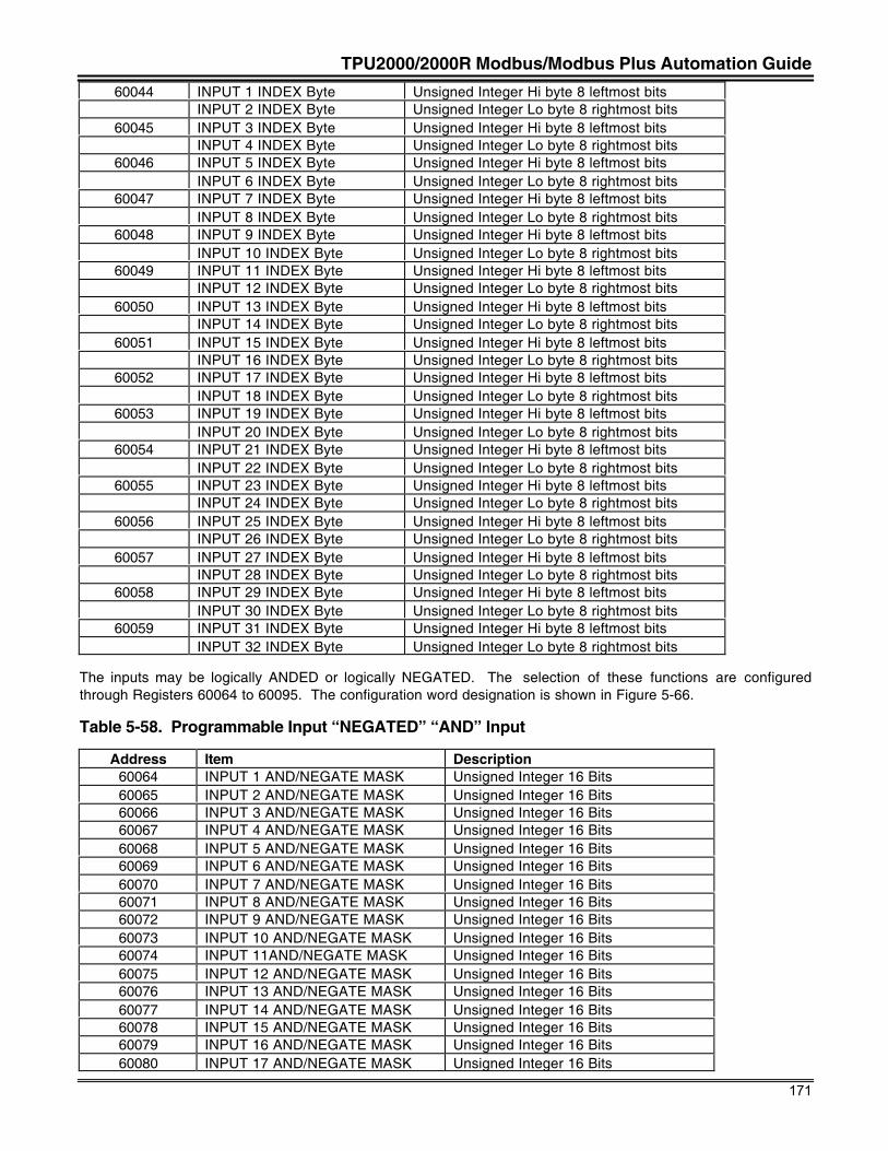
TPU2000/2000R Modbus/Modbus Plus Automation Guide
171
60044 INPUT 1 INDEX Byte Unsigned Integer Hi byte 8 leftmost bitsINPUT 2 INDEX Byte Unsigned Integer Lo byte 8 rightmost bits
60045 INPUT 3 INDEX Byte Unsigned Integer Hi byte 8 leftmost bitsINPUT 4 INDEX Byte Unsigned Integer Lo byte 8 rightmost bits
60046 INPUT 5 INDEX Byte Unsigned Integer Hi byte 8 leftmost bitsINPUT 6 INDEX Byte Unsigned Integer Lo byte 8 rightmost bits
60047 INPUT 7 INDEX Byte Unsigned Integer Hi byte 8 leftmost bitsINPUT 8 INDEX Byte Unsigned Integer Lo byte 8 rightmost bits
60048 INPUT 9 INDEX Byte Unsigned Integer Hi byte 8 leftmost bitsINPUT 10 INDEX Byte Unsigned Integer Lo byte 8 rightmost bits
60049 INPUT 11 INDEX Byte Unsigned Integer Hi byte 8 leftmost bitsINPUT 12 INDEX Byte Unsigned Integer Lo byte 8 rightmost bits
60050 INPUT 13 INDEX Byte Unsigned Integer Hi byte 8 leftmost bitsINPUT 14 INDEX Byte Unsigned Integer Lo byte 8 rightmost bits
60051 INPUT 15 INDEX Byte Unsigned Integer Hi byte 8 leftmost bitsINPUT 16 INDEX Byte Unsigned Integer Lo byte 8 rightmost bits
60052 INPUT 17 INDEX Byte Unsigned Integer Hi byte 8 leftmost bitsINPUT 18 INDEX Byte Unsigned Integer Lo byte 8 rightmost bits
60053 INPUT 19 INDEX Byte Unsigned Integer Hi byte 8 leftmost bitsINPUT 20 INDEX Byte Unsigned Integer Lo byte 8 rightmost bits
60054 INPUT 21 INDEX Byte Unsigned Integer Hi byte 8 leftmost bitsINPUT 22 INDEX Byte Unsigned Integer Lo byte 8 rightmost bits
60055 INPUT 23 INDEX Byte Unsigned Integer Hi byte 8 leftmost bitsINPUT 24 INDEX Byte Unsigned Integer Lo byte 8 rightmost bits
60056 INPUT 25 INDEX Byte Unsigned Integer Hi byte 8 leftmost bitsINPUT 26 INDEX Byte Unsigned Integer Lo byte 8 rightmost bits
60057 INPUT 27 INDEX Byte Unsigned Integer Hi byte 8 leftmost bitsINPUT 28 INDEX Byte Unsigned Integer Lo byte 8 rightmost bits
60058 INPUT 29 INDEX Byte Unsigned Integer Hi byte 8 leftmost bitsINPUT 30 INDEX Byte Unsigned Integer Lo byte 8 rightmost bits
60059 INPUT 31 INDEX Byte Unsigned Integer Hi byte 8 leftmost bitsINPUT 32 INDEX Byte Unsigned Integer Lo byte 8 rightmost bits
The inputs may be logically ANDED or logically NEGATED. The selection of these functions are configuredthrough Registers 60064 to 60095. The configuration word designation is shown in Figure 5-66.
Table 5-58. Programmable Input “NEGATED” “AND” Input
Address Item Description60064 INPUT 1 AND/NEGATE MASK Unsigned Integer 16 Bits60065 INPUT 2 AND/NEGATE MASK Unsigned Integer 16 Bits60066 INPUT 3 AND/NEGATE MASK Unsigned Integer 16 Bits60067 INPUT 4 AND/NEGATE MASK Unsigned Integer 16 Bits60068 INPUT 5 AND/NEGATE MASK Unsigned Integer 16 Bits60069 INPUT 6 AND/NEGATE MASK Unsigned Integer 16 Bits60070 INPUT 7 AND/NEGATE MASK Unsigned Integer 16 Bits60071 INPUT 8 AND/NEGATE MASK Unsigned Integer 16 Bits60072 INPUT 9 AND/NEGATE MASK Unsigned Integer 16 Bits60073 INPUT 10 AND/NEGATE MASK Unsigned Integer 16 Bits60074 INPUT 11AND/NEGATE MASK Unsigned Integer 16 Bits60075 INPUT 12 AND/NEGATE MASK Unsigned Integer 16 Bits60076 INPUT 13 AND/NEGATE MASK Unsigned Integer 16 Bits60077 INPUT 14 AND/NEGATE MASK Unsigned Integer 16 Bits60078 INPUT 15 AND/NEGATE MASK Unsigned Integer 16 Bits60079 INPUT 16 AND/NEGATE MASK Unsigned Integer 16 Bits60080 INPUT 17 AND/NEGATE MASK Unsigned Integer 16 Bits
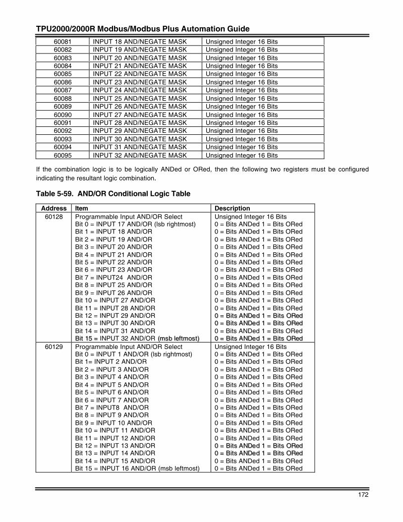
TPU2000/2000R Modbus/Modbus Plus Automation Guide
172
60081 INPUT 18 AND/NEGATE MASK Unsigned Integer 16 Bits60082 INPUT 19 AND/NEGATE MASK Unsigned Integer 16 Bits60083 INPUT 20 AND/NEGATE MASK Unsigned Integer 16 Bits60084 INPUT 21 AND/NEGATE MASK Unsigned Integer 16 Bits60085 INPUT 22 AND/NEGATE MASK Unsigned Integer 16 Bits60086 INPUT 23 AND/NEGATE MASK Unsigned Integer 16 Bits60087 INPUT 24 AND/NEGATE MASK Unsigned Integer 16 Bits60088 INPUT 25 AND/NEGATE MASK Unsigned Integer 16 Bits60089 INPUT 26 AND/NEGATE MASK Unsigned Integer 16 Bits60090 INPUT 27 AND/NEGATE MASK Unsigned Integer 16 Bits60091 INPUT 28 AND/NEGATE MASK Unsigned Integer 16 Bits60092 INPUT 29 AND/NEGATE MASK Unsigned Integer 16 Bits60093 INPUT 30 AND/NEGATE MASK Unsigned Integer 16 Bits60094 INPUT 31 AND/NEGATE MASK Unsigned Integer 16 Bits60095 INPUT 32 AND/NEGATE MASK Unsigned Integer 16 Bits
If the combination logic is to be logically ANDed or ORed, then the following two registers must be configuredindicating the resultant logic combination.
Table 5-59. AND/OR Conditional Logic Table
Address Item Description60128 Programmable Input AND/OR Select
Bit 0 = INPUT 17 AND/OR (lsb rightmost)Bit 1 = INPUT 18 AND/ORBit 2 = INPUT 19 AND/ORBit 3 = INPUT 20 AND/ORBit 4 = INPUT 21 AND/ORBit 5 = INPUT 22 AND/ORBit 6 = INPUT 23 AND/ORBit 7 = INPUT24 AND/ORBit 8 = INPUT 25 AND/ORBit 9 = INPUT 26 AND/ORBit 10 = INPUT 27 AND/ORBit 11 = INPUT 28 AND/ORBit 12 = INPUT 29 AND/ORBit 13 = INPUT 30 AND/ORBit 14 = INPUT 31 AND/ORBBiitt 1155 == INPUT 32 AND/OR ((mmssbb lleeff ttmmoosstt ))
Unsigned Integer 16 Bits0 = Bits ANDed 1 = Bits ORed0 = Bits ANDed 1 = Bits ORed0 = Bits ANDed 1 = Bits ORed0 = Bits ANDed 1 = Bits ORed0 = Bits ANDed 1 = Bits ORed0 = Bits ANDed 1 = Bits ORed0 = Bits ANDed 1 = Bits ORed0 = Bits ANDed 1 = Bits ORed0 = Bits ANDed 1 = Bits ORed0 = Bits ANDed 1 = Bits ORed0 = Bits ANDed 1 = Bits ORed0 = Bits ANDed 1 = Bits ORed00 == BBiittss AANNDDeedd 11 == BBiittss OORReedd00 == BBiittss AANNDDeedd 11 == BBiittss OORReedd0 = Bits ANDed 1 = Bits ORed00 == BBiittss AANNDDeedd 11 == BBiittss OORReedd
60129 Programmable Input AND/OR SelectBit 0 = INPUT 1 AND/OR (lsb rightmost)Bit 1= INPUT 2 AND/ORBit 2 = INPUT 3 AND/ORBit 3 = INPUT 4 AND/ORBit 4 = INPUT 5 AND/ORBit 5 = INPUT 6 AND/ORBit 6 = INPUT 7 AND/ORBit 7 = INPUT8 AND/ORBit 8 = INPUT 9 AND/ORBit 9 = INPUT 10 AND/ORBit 10 = INPUT 11 AND/ORBit 11 = INPUT 12 AND/ORBit 12 = INPUT 13 AND/ORBit 13 = INPUT 14 AND/ORBit 14 = INPUT 15 AND/ORBit 15 = INPUT 16 AND/OR (msb leftmost)
Unsigned Integer 16 Bits0 = Bits ANDed 1 = Bits ORed0 = Bits ANDed 1 = Bits ORed0 = Bits ANDed 1 = Bits ORed0 = Bits ANDed 1 = Bits ORed0 = Bits ANDed 1 = Bits ORed0 = Bits ANDed 1 = Bits ORed0 = Bits ANDed 1 = Bits ORed0 = Bits ANDed 1 = Bits ORed0 = Bits ANDed 1 = Bits ORed0 = Bits ANDed 1 = Bits ORed0 = Bits ANDed 1 = Bits ORed0 = Bits ANDed 1 = Bits ORed00 == BBiittss AANNDDeedd 11 == BBiittss OORReedd00 == BBiittss AANNDDeedd 11 == BBiittss OORReedd0 = Bits ANDed 1 = Bits ORed0 = Bits ANDed 1 = Bits ORed
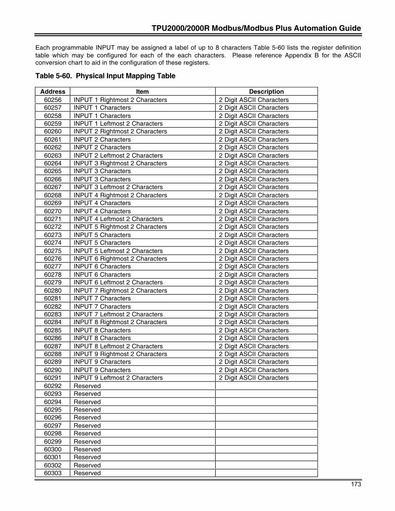
TPU2000/2000R Modbus/Modbus Plus Automation Guide
173
Each programmable INPUT may be assigned a label of up to 8 characters Table 5-60 lists the register definitiontable which may be configured for each of the each characters. Please reference Appendix B for the ASCIIconversion chart to aid in the configuration of these registers.
Table 5-60. Physical Input Mapping Table
Address Item Description60256 INPUT 1 Rightmost 2 Characters 2 Digit ASCII Characters60257 INPUT 1 Characters 2 Digit ASCII Characters60258 INPUT 1 Characters 2 Digit ASCII Characters60259 INPUT 1 Leftmost 2 Characters 2 Digit ASCII Characters60260 INPUT 2 Rightmost 2 Characters 2 Digit ASCII Characters60261 INPUT 2 Characters 2 Digit ASCII Characters60262 INPUT 2 Characters 2 Digit ASCII Characters60263 INPUT 2 Leftmost 2 Characters 2 Digit ASCII Characters60264 INPUT 3 Rightmost 2 Characters 2 Digit ASCII Characters60265 INPUT 3 Characters 2 Digit ASCII Characters60266 INPUT 3 Characters 2 Digit ASCII Characters60267 INPUT 3 Leftmost 2 Characters 2 Digit ASCII Characters60268 INPUT 4 Rightmost 2 Characters 2 Digit ASCII Characters60269 INPUT 4 Characters 2 Digit ASCII Characters60270 INPUT 4 Characters 2 Digit ASCII Characters60271 INPUT 4 Leftmost 2 Characters 2 Digit ASCII Characters60272 INPUT 5 Rightmost 2 Characters 2 Digit ASCII Characters60273 INPUT 5 Characters 2 Digit ASCII Characters60274 INPUT 5 Characters 2 Digit ASCII Characters60275 INPUT 5 Leftmost 2 Characters 2 Digit ASCII Characters60276 INPUT 6 Rightmost 2 Characters 2 Digit ASCII Characters60277 INPUT 6 Characters 2 Digit ASCII Characters60278 INPUT 6 Characters 2 Digit ASCII Characters60279 INPUT 6 Leftmost 2 Characters 2 Digit ASCII Characters60280 INPUT 7 Rightmost 2 Characters 2 Digit ASCII Characters60281 INPUT 7 Characters 2 Digit ASCII Characters60282 INPUT 7 Characters 2 Digit ASCII Characters60283 INPUT 7 Leftmost 2 Characters 2 Digit ASCII Characters60284 INPUT 8 Rightmost 2 Characters 2 Digit ASCII Characters60285 INPUT 8 Characters 2 Digit ASCII Characters60286 INPUT 8 Characters 2 Digit ASCII Characters60287 INPUT 8 Leftmost 2 Characters 2 Digit ASCII Characters60288 INPUT 9 Rightmost 2 Characters 2 Digit ASCII Characters60289 INPUT 9 Characters 2 Digit ASCII Characters60290 INPUT 9 Characters 2 Digit ASCII Characters60291 INPUT 9 Leftmost 2 Characters 2 Digit ASCII Characters60292 Reserved60293 Reserved60294 Reserved60295 Reserved60296 Reserved60297 Reserved60298 Reserved60299 Reserved60300 Reserved60301 Reserved60302 Reserved60303 Reserved
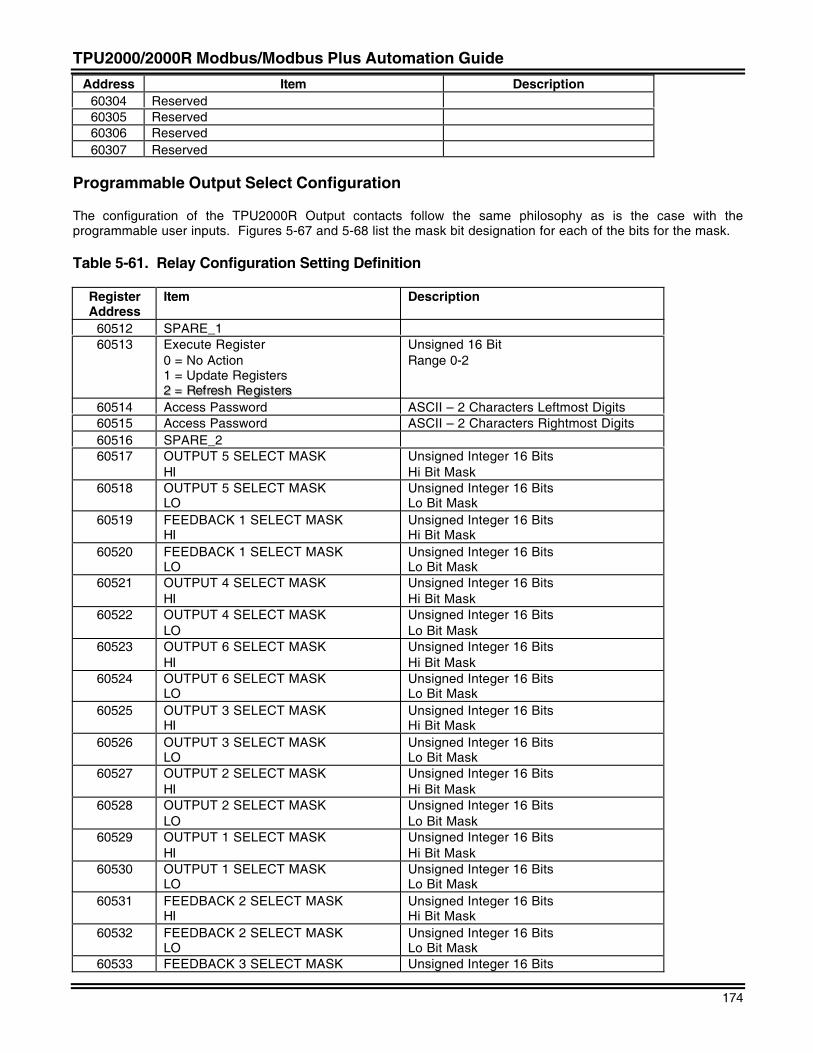
TPU2000/2000R Modbus/Modbus Plus Automation Guide
174
Address Item Description60304 Reserved60305 Reserved60306 Reserved60307 Reserved
Programmable Output Select Configuration
The configuration of the TPU2000R Output contacts follow the same philosophy as is the case with theprogrammable user inputs. Figures 5-67 and 5-68 list the mask bit designation for each of the bits for the mask.
Table 5-61. Relay Configuration Setting Definition
RegisterAddress
Item Description
60512 SPARE_160513 Execute Register
0 = No Action1 = Update Registers22 == RReeff rreesshh RReeggiiss tteerrss
Unsigned 16 BitRange 0-2
60514 Access Password ASCII – 2 Characters Leftmost Digits60515 Access Password ASCII – 2 Characters Rightmost Digits60516 SPARE_260517 OUTPUT 5 SELECT MASK
HIUnsigned Integer 16 BitsHi Bit Mask
60518 OUTPUT 5 SELECT MASKLO
Unsigned Integer 16 BitsLo Bit Mask
60519 FEEDBACK 1 SELECT MASKHI
Unsigned Integer 16 BitsHi Bit Mask
60520 FEEDBACK 1 SELECT MASKLO
Unsigned Integer 16 BitsLo Bit Mask
60521 OUTPUT 4 SELECT MASKHI
Unsigned Integer 16 BitsHi Bit Mask
60522 OUTPUT 4 SELECT MASKLO
Unsigned Integer 16 BitsLo Bit Mask
60523 OUTPUT 6 SELECT MASKHI
Unsigned Integer 16 BitsHi Bit Mask
60524 OUTPUT 6 SELECT MASKLO
Unsigned Integer 16 BitsLo Bit Mask
60525 OUTPUT 3 SELECT MASKHI
Unsigned Integer 16 BitsHi Bit Mask
60526 OUTPUT 3 SELECT MASKLO
Unsigned Integer 16 BitsLo Bit Mask
60527 OUTPUT 2 SELECT MASKHI
Unsigned Integer 16 BitsHi Bit Mask
60528 OUTPUT 2 SELECT MASKLO
Unsigned Integer 16 BitsLo Bit Mask
60529 OUTPUT 1 SELECT MASKHI
Unsigned Integer 16 BitsHi Bit Mask
60530 OUTPUT 1 SELECT MASKLO
Unsigned Integer 16 BitsLo Bit Mask
60531 FEEDBACK 2 SELECT MASKHI
Unsigned Integer 16 BitsHi Bit Mask
60532 FEEDBACK 2 SELECT MASKLO
Unsigned Integer 16 BitsLo Bit Mask
60533 FEEDBACK 3 SELECT MASK Unsigned Integer 16 Bits
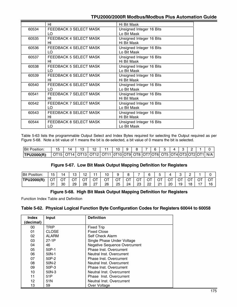
TPU2000/2000R Modbus/Modbus Plus Automation Guide
175
HI Hi Bit Mask60534 FEEDBACK 3 SELECT MASK
LOUnsigned Integer 16 BitsLo Bit Mask
60535 FEEDBACK 4 SELECT MASKHI
Unsigned Integer 16 BitsHi Bit Mask
60536 FEEDBACK 4 SELECT MASKLO
Unsigned Integer 16 BitsLo Bit Mask
60537 FEEDBACK 5 SELECT MASKHI
Unsigned Integer 16 BitsHi Bit Mask
60538 FEEDBACK 5 SELECT MASKLO
Unsigned Integer 16 BitsLo Bit Mask
60539 FEEDBACK 6 SELECT MASKHI
Unsigned Integer 16 BitsHi Bit Mask
60540 FEEDBACK 6 SELECT MASKLO
Unsigned Integer 16 BitsLo Bit Mask
60541 FEEDBACK 7 SELECT MASKHI
Unsigned Integer 16 BitsHi Bit Mask
60542 FEEDBACK 7 SELECT MASKLO
Unsigned Integer 16 BitsLo Bit Mask
60543 FEEDBACK 8 SELECT MASKHI
Unsigned Integer 16 BitsHi Bit Mask
60544 FEEDBACK 8 SELECT MASKLO
Unsigned Integer 16 BitsLo Bit Mask
Table 5-63 lists the programmable Output Select and Index Bytes required for selecting the Output required as perFigure 5-68. Note a bit value of 1 means the bit is de-selected, a bit value of 0 means the bit is selected.
Bit Position: 15 14 13 12 11 10 9 8 7 6 5 4 3 2 1 0TPU2000(R): OT15 OT14 OT13 OT12 OT11 0T10 OT9 OT8 OT7 OT6 OT5 OT4 OT3 OT2 OT1 N/A
Figure 5-67. Low Bit Mask Output Mapping Definition for Registers
Bit Position: 15 14 13 12 11 10 9 8 7 6 5 4 3 2 1 0TPU2000(R): OT
31OT30
OT29
OT28
OT27
OT26
OT25
OT24
OT23
OT 22
OT21
OT20
OT19
OT18
OT17
OT16
Figure 5-68. High Bit Mask Output Mapping Definition for RegistersFunction Index Table and Definition
Table 5-62. Physical Logical Function Byte Configuration Codes for Registers 60044 to 60058
Index(decimal)
Input Definition
0001020304050607080910111213
TRIPCLOSEALARM27-1P4650P-150N-150P-250N-250P-350N-351P51N59
Fixed TripFixed CloseSelf Check AlarmSingle Phase Under VoltageNegative Sequence OvercurrentPhase Inst. OvercurrentNeutral Inst. OvercurrentPhase Inst. OvercurrentNeutral Inst. OvercurrentPhase Inst. OvercurrentNeutral Inst. OvercurrentPhase Inst. OvercurrentNeutral Inst. OvercurrentOver Voltage
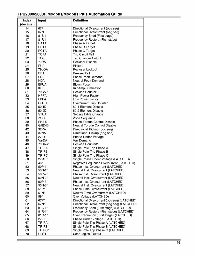
TPU2000/2000R Modbus/Modbus Plus Automation Guide
176
Index(decimal)
Input Definition
1415161718192021222324252627282930313233343536373839404243444546474849505152535455565758596061626364656667686970
67P67N81S-181R-1PATAPBTAPCTATCFATCC79DAPUA79LOABFAPDANDABFUAKSI79CA-1HPFALPFAOCTC50-1D50-2DSTCAZSCPH3-DGRD-D32PA32NA27-3PVarDA79CA-2TRIPATRIPBTRIPC27-1P*46*50P-1*50N-1*50P-2*50N-2*50P-3*50N-3*51P*51N*59*67P*67N*81S-1*81R-1*81O-1*27-3P*TRIPA*TRIPB*TRIPC*ULO1
Directional Overcurrent (pos seq)Directional Overcurrent (neg seq)Frequency Shed (First stage)Frequency Restore (First stage)Phase A Target Phase B Target Phase C TargetTrip Circuit FailTap Changer CutoutRecloser DisablePickupRecloser LockoutBreaker FailPhase Peak DemandNeutral Peak DemandBlown FuseKiloAmp SummationReclose Counter1High Power FactorLow Power FactorOvercurrent Trip Counter50-1 Element Disable50-2 Element DisableSetting Table ChangeZone SequencePhase Torque Control DisableNeutral Torque Control DisableDirectional Pickup (pos seq)Directional Pickup (neg seq)Phase Under VoltageVar DemandReclose Counter2Single Pole Trip Phase ASingle Pole Trip Phase BSingle Pole Trip Phase CSingle Phase Under Voltage (LATCHED)Negative Sequence Overcurrent (LATCHED)Phase Inst. Overcurrent (LATCHED)Neutral Inst. Overcurrent (LATCHED)Phase Inst. Overcurrent (LATCHED)Neutral Inst. Overcurrent (LATCHED)Phase Inst. Overcurrent (LATCHED)Neutral Inst. Overcurrent (LATCHED)Phase Time Overcurrent (LATCHED)Neutral Time Overcurrent (LATCHED)Over Voltage (LATCHED)Directional Overcurrent (pos seq) (LATCHED)Directional Overcurrent (neg seq) (LATCHED)Frequency Shed (First stage) (LATCHED)Frequency Restore (First stage) (LATCHED)Over Frequency (First stage) (LATCHED)Phase Under Voltage (LATCHED)Single Pole Trip Phase A (LATCHED)Single Pole Trip Phase B (LATCHED)Single Pole Trip Phase C (LATCHED)User Logical Output 1
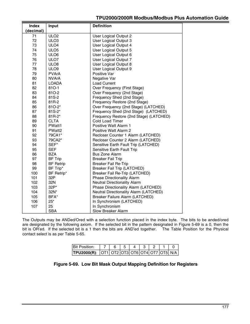
TPU2000/2000R Modbus/Modbus Plus Automation Guide
177
Index(decimal)
Input Definition
7172737475767778798081828384858687888990919293949586979899
100101102103104105106107
ULO2ULO3ULO4ULO5ULO6ULO7ULO8ULO9PVArANVArALOADA81O-181O-281S-281R-281O-2*81S-2*81R-2*CLTAPWatt1PWatt279CA1*79CA2*SEF*SEFBZABF Trip BF RetripBF Trip*BF Retrip*32P32N32P*32N*BFA*25*25SBA
User Logical Output 2User Logical Output 3User Logical Output 4User Logical Output 5User Logical Output 6User Logical Output 7User Logical Output 8User Logical Output 9Positive VarNegative VarLoad CurrentOver Frequency (First Stage)Over Frequency (2nd Stage)Frequency Shed (2nd Stage)Frequency Restore (2nd Stage)Over Frequency (2nd Stage) (LATCHED)Frequency Shed (2nd Stage) (LATCHED)Frequency Restore (2nd Stage) (LATCHED)Cold Load TimerPositive Watt Alarm 1Positive Watt Alarm 2Recloser Counter 1 Alarm (LATCHED)Recloser Counter 2 Alarm (LATCHED)Sensitive Earth Fault Trip (LATCHED)Sensitive Earth Fault TripBus Zone AlarmBreaker Fail TripBreaker Fail Re-TripBreaker Fail Trip (LATCHED)Breaker Fail Re-Trip (LATCHED)Phase Directionality AlarmNeutral Directionality AlarmPhase Directionality Alarm (LATCHED)Neutral Directionality Alarm (LATCHED)Breaker Failure Alarm (LATCHED)In Synchronism (LATCHED)In SynchronismSlow Breaker Alarm
The Outputs may be ANDed/Ored with a selection function placed in the index byte. The bits to be anded/oredare designated by the following axiom. If the selected bit in the pattern designated in Figure 5-69 is a 0, then thebit is OR’ed. If the selected bit is a 1 then the bits are AND’ed together. The Table Position for the Physicalcontact select is as per Table 5-65.
Bit Position: 7 6 5 4 3 2 1 0TPU2000(R): OT1 OT2 OT3 OT6 OT4 OT7 OT5 N/A
Figure 5-69. Low Bit Mask Output Mapping Definition for Registers
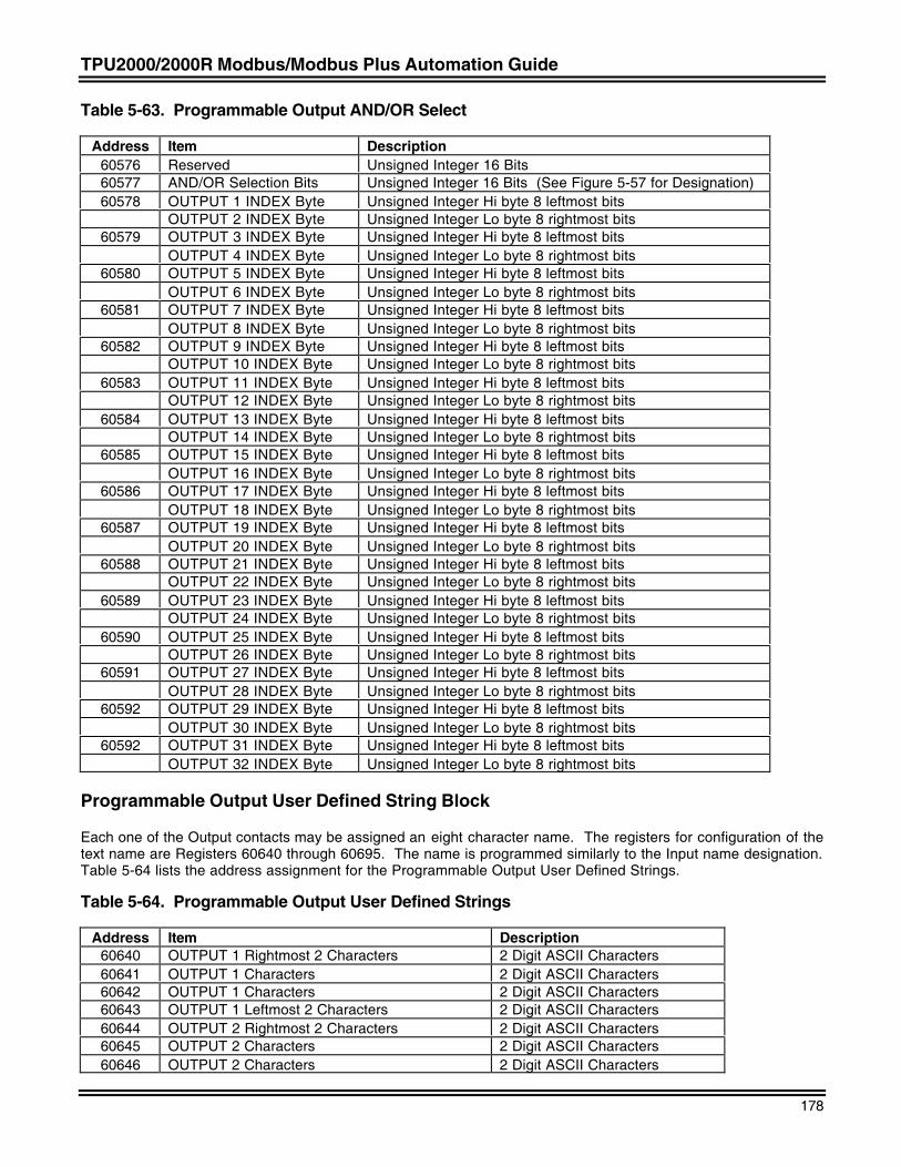
TPU2000/2000R Modbus/Modbus Plus Automation Guide
178
Table 5-63. Programmable Output AND/OR Select
Address Item Description60576 Reserved Unsigned Integer 16 Bits60577 AND/OR Selection Bits Unsigned Integer 16 Bits (See Figure 5-57 for Designation)60578 OUTPUT 1 INDEX Byte Unsigned Integer Hi byte 8 leftmost bits
OUTPUT 2 INDEX Byte Unsigned Integer Lo byte 8 rightmost bits60579 OUTPUT 3 INDEX Byte Unsigned Integer Hi byte 8 leftmost bits
OUTPUT 4 INDEX Byte Unsigned Integer Lo byte 8 rightmost bits60580 OUTPUT 5 INDEX Byte Unsigned Integer Hi byte 8 leftmost bits
OUTPUT 6 INDEX Byte Unsigned Integer Lo byte 8 rightmost bits60581 OUTPUT 7 INDEX Byte Unsigned Integer Hi byte 8 leftmost bits
OUTPUT 8 INDEX Byte Unsigned Integer Lo byte 8 rightmost bits60582 OUTPUT 9 INDEX Byte Unsigned Integer Hi byte 8 leftmost bits
OUTPUT 10 INDEX Byte Unsigned Integer Lo byte 8 rightmost bits60583 OUTPUT 11 INDEX Byte Unsigned Integer Hi byte 8 leftmost bits
OUTPUT 12 INDEX Byte Unsigned Integer Lo byte 8 rightmost bits60584 OUTPUT 13 INDEX Byte Unsigned Integer Hi byte 8 leftmost bits
OUTPUT 14 INDEX Byte Unsigned Integer Lo byte 8 rightmost bits60585 OUTPUT 15 INDEX Byte Unsigned Integer Hi byte 8 leftmost bits
OUTPUT 16 INDEX Byte Unsigned Integer Lo byte 8 rightmost bits60586 OUTPUT 17 INDEX Byte Unsigned Integer Hi byte 8 leftmost bits
OUTPUT 18 INDEX Byte Unsigned Integer Lo byte 8 rightmost bits60587 OUTPUT 19 INDEX Byte Unsigned Integer Hi byte 8 leftmost bits
OUTPUT 20 INDEX Byte Unsigned Integer Lo byte 8 rightmost bits60588 OUTPUT 21 INDEX Byte Unsigned Integer Hi byte 8 leftmost bits
OUTPUT 22 INDEX Byte Unsigned Integer Lo byte 8 rightmost bits60589 OUTPUT 23 INDEX Byte Unsigned Integer Hi byte 8 leftmost bits
OUTPUT 24 INDEX Byte Unsigned Integer Lo byte 8 rightmost bits60590 OUTPUT 25 INDEX Byte Unsigned Integer Hi byte 8 leftmost bits
OUTPUT 26 INDEX Byte Unsigned Integer Lo byte 8 rightmost bits60591 OUTPUT 27 INDEX Byte Unsigned Integer Hi byte 8 leftmost bits
OUTPUT 28 INDEX Byte Unsigned Integer Lo byte 8 rightmost bits60592 OUTPUT 29 INDEX Byte Unsigned Integer Hi byte 8 leftmost bits
OUTPUT 30 INDEX Byte Unsigned Integer Lo byte 8 rightmost bits60592 OUTPUT 31 INDEX Byte Unsigned Integer Hi byte 8 leftmost bits
OUTPUT 32 INDEX Byte Unsigned Integer Lo byte 8 rightmost bits
Programmable Output User Defined String Block
Each one of the Output contacts may be assigned an eight character name. The registers for configuration of thetext name are Registers 60640 through 60695. The name is programmed similarly to the Input name designation.Table 5-64 lists the address assignment for the Programmable Output User Defined Strings.
Table 5-64. Programmable Output User Defined Strings
Address Item Description60640 OUTPUT 1 Rightmost 2 Characters 2 Digit ASCII Characters60641 OUTPUT 1 Characters 2 Digit ASCII Characters60642 OUTPUT 1 Characters 2 Digit ASCII Characters60643 OUTPUT 1 Leftmost 2 Characters 2 Digit ASCII Characters60644 OUTPUT 2 Rightmost 2 Characters 2 Digit ASCII Characters60645 OUTPUT 2 Characters 2 Digit ASCII Characters60646 OUTPUT 2 Characters 2 Digit ASCII Characters
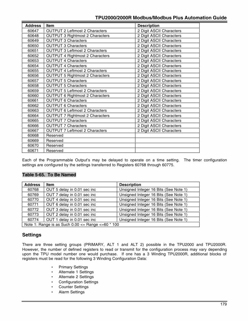
TPU2000/2000R Modbus/Modbus Plus Automation Guide
179
Address Item Description60647 OUTPUT 2 Leftmost 2 Characters 2 Digit ASCII Characters60648 OUTPUT 3 Rightmost 2 Characters 2 Digit ASCII Characters60649 OUTPUT 3 Characters 2 Digit ASCII Characters60650 OUTPUT 3 Characters 2 Digit ASCII Characters60651 OUTPUT 3 Leftmost 2 Characters 2 Digit ASCII Characters60652 OUTPUT 4 Rightmost 2 Characters 2 Digit ASCII Characters60653 OUTPUT 4 Characters 2 Digit ASCII Characters60654 OUTPUT 4 Characters 2 Digit ASCII Characters60655 OUTPUT 4 Leftmost 2 Characters 2 Digit ASCII Characters60656 OUTPUT 5 Rightmost 2 Characters 2 Digit ASCII Characters60657 OUTPUT 5 Characters 2 Digit ASCII Characters60658 OUTPUT 5 Characters 2 Digit ASCII Characters60659 OUTPUT 5 Leftmost 2 Characters 2 Digit ASCII Characters60660 OUTPUT 6 Rightmost 2 Characters 2 Digit ASCII Characters60661 OUTPUT 6 Characters 2 Digit ASCII Characters60662 OUTPUT 6 Characters 2 Digit ASCII Characters60663 OUTPUT 6 Leftmost 2 Characters 2 Digit ASCII Characters60664 OUTPUT 7 Rightmost 2 Characters 2 Digit ASCII Characters60665 OUTPUT 7 Characters 2 Digit ASCII Characters60666 OUTPUT 7 Characters 2 Digit ASCII Characters60667 OUTPUT 7 Leftmost 2 Characters 2 Digit ASCII Characters60668 Reserved60669 Reserved60670 Reserved60671 Reserved
Each of the Programmable Output’s may be delayed to operate on a time setting. The timer configurationsettings are configured by the settings transferred to Registers 60768 through 60775.
Table 5-65. To Be Named
Address Item Description60768 OUT 5 delay in 0.01 sec inc Unsigned Integer 16 Bits (See Note 1)60769 OUT 7 delay in 0.01 sec inc Unsigned Integer 16 Bits (See Note 1)60770 OUT 4 delay in 0.01 sec inc Unsigned Integer 16 Bits (See Note 1)60771 OUT 6 delay in 0.01 sec inc Unsigned Integer 16 Bits (See Note 1)60772 OUT 3 delay in 0.01 sec inc Unsigned Integer 16 Bits (See Note 1)60773 OUT 2 delay in 0.01 sec inc Unsigned Integer 16 Bits (See Note 1)60774 OUT 1 delay in 0.01 sec inc Unsigned Integer 16 Bits (See Note 1)
Note 1: Range is as Such 0.00 <= Range <=60 * 100
Settings
There are three setting groups (PRIMARY, ALT 1 and ALT 2) possible in the TPU2000 and TPU2000R.However, the number of defined registers to read or transmit for the configuration process may vary dependingupon the TPU model number one would purchase. If one has a 3 Winding TPU2000R, additional blocks ofregisters must be read for the following 3 Winding Configuration Data:
• Primary Settings• Alternate 1 Settings• Alternate 2 Settings• Configuration Settings• Counter Settings• Alarm Settings
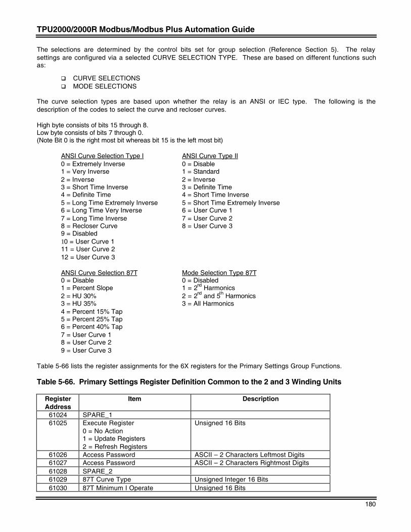
TPU2000/2000R Modbus/Modbus Plus Automation Guide
180
The selections are determined by the control bits set for group selection (Reference Section 5). The relaysettings are configured via a selected CURVE SELECTION TYPE. These are based on different functions suchas:
q CURVE SELECTIONSq MODE SELECTIONS
The curve selection types are based upon whether the relay is an ANSI or IEC type. The following is thedescription of the codes to select the curve and recloser curves.
High byte consists of bits 15 through 8.Low byte consists of bits 7 through 0.(Note Bit 0 is the right most bit whereas bit 15 is the left most bit)
ANSI Curve Selection Type I ANSI Curve Type II0 = Extremely Inverse 0 = Disable1 = Very Inverse 1 = Standard2 = Inverse 2 = Inverse3 = Short Time Inverse 3 = Definite Time4 = Definite Time 4 = Short Time Inverse5 = Long Time Extremely Inverse 5 = Short Time Extremely Inverse6 = Long Time Very Inverse 6 = User Curve 17 = Long Time Inverse 7 = User Curve 28 = Recloser Curve 8 = User Curve 39 = Disabled10 = User Curve 111 = User Curve 212 = User Curve 3
ANSI Curve Selection 87T Mode Selection Type 87T0 = Disable 0 = Disabled1 = Percent Slope 1 = 2nd Harmonics2 = HU 30% 2 = 2nd and 5th Harmonics3 = HU 35% 3 = All Harmonics4 = Percent 15% Tap5 = Percent 25% Tap6 = Percent 40% Tap7 = User Curve 18 = User Curve 29 = User Curve 3
Table 5-66 lists the register assignments for the 6X registers for the Primary Settings Group Functions.
Table 5-66. Primary Settings Register Definition Common to the 2 and 3 Winding Units
RegisterAddress
Item Description
61024 SPARE_161025 Execute Register
0 = No Action1 = Update Registers2 = Refresh Registers
Unsigned 16 Bits
61026 Access Password ASCII – 2 Characters Leftmost Digits61027 Access Password ASCII – 2 Characters Rightmost Digits61028 SPARE_261029 87T Curve Type Unsigned Integer 16 Bits61030 87T Minimum I Operate Unsigned 16 Bits
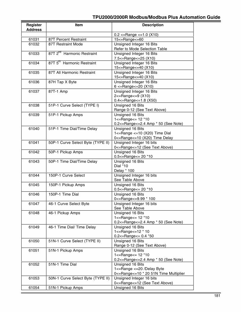
TPU2000/2000R Modbus/Modbus Plus Automation Guide
181
RegisterAddress
Item Description
0.2 <=Range <=1.0 (X10)61031 87T Percent Restraint 15<=Range<=6061032 87T Restraint Mode Unsigned Integer 16 Bits
Refer to Mode Selection Table61033 87T 2nd Harmonic Restraint Unsigned Integer 16 Bits
7.5<=Range<=25 (X10)61034 87T 5th Harmonic Restraint Unsigned Integer 16 Bits
15<=Range<=40 (X10)61035 87T All Harmonic Restraint Unsigned Integer 16 Bits
15<=Range<=40 (X10)61036 87H Tap X Byte Unsigned Integer 16 Bits
6 <=Range<=20 (X10)61037 87T-1 Amp Unsigned Integer 16 Bits
2<=Range<=9 (X10)0.4<=Range<=1.8 (X50)
61038 51P-1 Curve Select (TYPE I) Unsigned 16 BitsRange 0-12 (See Text Above)
61039 51P-1 Pickup Amps Unsigned 16 Bits1<=Range<= 12 *100.2<=Range<=2.4 Amp * 50 (See Note)
61040 51P-1 Time Dial/Time Delay Unsigned 16 Bits1<=Range <=10 (X20) Time Dial0<=Range<=10 (X20) Time Delay
61041 50P-1 Curve Select Byte (TYPE II) Unsigned Integer 16 bits0<=Range<=12 (See Text Above)
61042 50P-1 Pickup Amps Unsigned 16 Bits0.5<=Range<= 20 *10
61043 50P-1 Time Dial/Time Delay Unsigned 16 BitsDial *10Delay * 100
61044 150P-1 Curve Select Unsigned Integer 16 bitsSee Table Above
61045 150P-1 Pickup Amps Unsigned 16 Bits0.5<=Range<= 20 *10
61046 150P-1 Time Dial Unsigned 16 Bits0<=Range<=9.99 * 100
61047 46-1 Curve Select Byte Unsigned Integer 16 bitsSee Table Above
61048 46-1 Pickup Amps Unsigned 16 Bits1<=Range<= 12 *100.2<=Range<=2.4 Amp * 50 (See Note)
61049 46-1 Time Dial/ Time Delay Unsigned 16 Bits1<=Range<=12 * 100.2<=Range<= 0.4 *50
61050 51N-1 Curve Select (TYPE II) Unsigned 16 BitsRange 0-12 (See Text Above)
61051 51N-1 Pickup Amps Unsigned 16 Bits1<=Range<= 12 *100.2<=Range<=2.4 Amp * 50 (See Note)
61052 51N-1 Time Dial Unsigned 16 Bits1<=Range <=20 /Delay Byte0<=Range<=10 * 20 51N Time Multiplier
61053 50N-1 Curve Select Byte (TYPE II) Unsigned Integer 16 bits0<=Range<=12 (See Text Above)
61054 51N-1 Pickup Amps Unsigned 16 Bits
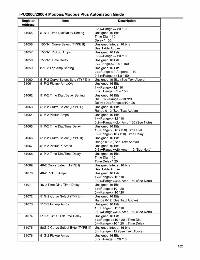
TPU2000/2000R Modbus/Modbus Plus Automation Guide
182
RegisterAddress
Item Description
0.5<=Range<= 20 *1061055 51N-1 Time Dial/Delay Setting Unsigned 16 Bits
Time Dial * 10Delay * 100
61056 150N-1 Curve Select (TYPE II) Unsigned Integer 16 bitsSee Table Above
61057 150N-1 Pickup Amps Unsigned 16 Bits0.5<=Range<= 20 *10
61058 150N-1 Time Delay Unsigned 16 Bits0<=Range<=9.99 * 100
61059 87T-2 Tap Amp Setting Unsigned 16 Bits2<=Range<=9 Amperes * 100.4<=Range <=1.8 * 50
61060 51P-2 Curve Select Byte (TYPE I) Unsigned 16 Bits (See Text Above)61061 51P-2 Pickup Amp/OA Unsigned 16 Bits
1<=Range<=12 *100.2<=Range<=2.4 * 50
61062 51P-2 Time Dial /Delay Setting Unsigned 16 BitsDial : 1<=Range<=10 *20Delay : 0<=Range<=10 * 20
61063 51P-2 Curve Select (TYPE I ) Unsigned 16 BitsRange 0-12 (See Text Above)
61064 51P-2 Pickup Amps Unsigned 16 Bits1<=Range<= 12 *100.2<=Range<=2.4 Amp * 50 (See Note)
61065 51P-2 Time Dial/Time Delay Unsigned 16 Bits1<=Range <=10 (X20) Time Dial0<=Range<=10 (X20) Time Delay
61066 51P-2 Curve Select (TYPE II) Unsigned 16 BitsRange 0-12 ( See Text Above)
61067 51P-2 Pickup X Amps Unsigned 16 Bits0.5<=Range<=20 Amp * 10 (See Note)
61068 51P-2 Time Dial/Time Delay Unsigned 16 BitsTime Dial * 10Time Delay * 20
61069 46-2 Curve Select (TYPE I) Unsigned Integer 16 bitsSee Table Above
61070 46-2 Pickup Amps Unsigned 16 Bits1<=Range<= 12 *100.2<=Range<=2.4 Amp * 50 (See Note)
61071 46-2 Time Dial/ Time Delay Unsigned 16 Bits1<=Range<=10 * 200<=Range<= 10 *20
61072 51G-2 Curve Select (TYPE II) Unsigned 16 BitsRange 0-12 (See Text Above)
61073 51G-2 Pickup Amps Unsigned 16 Bits1<=Range<= 12 *100.2<=Range<=2.4 Amp * 50 (See Note)
61074 51G-2 Time Dial/Time Delay Unsigned 16 Bits1<=Range <=10 * 20 : Time Dial0<=Range<=10 * 20 : Time Delay
61075 50G-2 Curve Select Byte (TYPE II) Unsigned Integer 16 bits0<=Range<=12 (See Text Above)
61076 51G-2 Pickup Amps Unsigned 16 Bits0.5<=Range<= 20 *10
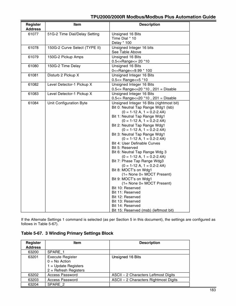
TPU2000/2000R Modbus/Modbus Plus Automation Guide
183
RegisterAddress
Item Description
61077 51G-2 Time Dial/Delay Setting Unsigned 16 BitsTime Dial * 10Delay * 100
61078 150G-2 Curve Select (TYPE II) Unsigned Integer 16 bitsSee Table Above
61079 150G-2 Pickup Amps Unsigned 16 Bits0.5<=Range<= 20 *10
61080 150G-2 Time Delay Unsigned 16 Bits0<=Range<=9.99 * 100
61081 Disturb 2 Pickup X Unsigned Integer 16 Bits0.5<= Range<=5 *10
61082 Level Detector-1 Pickup X Unsigned Integer 16 Bits0.5<= Range<=20 *10 , 201 = Disable
61083 Level Detector-1 Pickup X Unsigned Integer 16 Bits0.5<= Range<=20 *10 , 201 = Disable
61084 Unit Configuration Byte Unsigned Integer 16 Bits (rightmost bit)Bit 0: Neutral Tap Range Wdg1 (lsb) (0 = 1-12 A, 1 = 0.2-2.4A)Bit 1: Neutral Tap Range Wdg1 (0 = 1-12 A, 1 = 0.2-2.4A)Bit 2: Neutral Tap Range Wdg1 (0 = 1-12 A, 1 = 0.2-2.4A)Bit 3: Neutral Tap Range Wdg1 (0 = 1-12 A, 1 = 0.2-2.4A)Bit 4: User Definable CurvesBit 5: ReservedBit 6: Neutral Tap Range Wdg 3 (0 = 1-12 A, 1 = 0.2-2.4A)Bit 7: Phase Tap Range Wdg3 (0 = 1-12 A, 1 = 0.2-2.4A)Bit 8: MOCT’s on Wdg1 (1= None 0= MOCT Present)Bit 9: MOCT’s on Wdg1 (1= None 0= MOCT Present)Bit 10: ReservedBit 11: ReservedBit 12: ReservedBit 13: ReservedBit 14: ReservedBit 15: Reserved (msb) (leftmost bit)
If the Alternate Settings 1 command is selected (as per Section 5 in this document), the settings are configured asfollows in Table 5-67).
Table 5-67. 3 Winding Primary Settings Block
RegisterAddress
Item Description
63200 SPARE_163201 Execute Register
0 = No Action1 = Update Registers2 = Refresh Registers
UUnnss iiggnneedd 1166 BBiittss
63202 Access Password ASCII – 2 Characters Leftmost Digits63203 Access Password ASCII – 2 Characters Rightmost Digits63204 SPARE_2
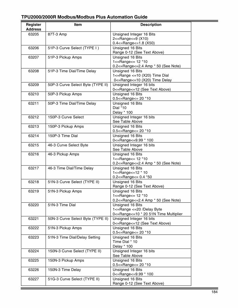
TPU2000/2000R Modbus/Modbus Plus Automation Guide
184
RegisterAddress
Item Description
63205 87T-3 Amp Unsigned Integer 16 Bits2<=Range<=9 (X10)0.4<=Range<=1.8 (X50)
63206 51P-3 Curve Select (TYPE I ) Unsigned 16 BitsRange 0-12 (See Text Above)
63207 51P-3 Pickup Amps Unsigned 16 Bits1<=Range<= 12 *100.2<=Range<=2.4 Amp * 50 (See Note)
63208 51P-3 Time Dial/Time Delay Unsigned 16 Bits1<=Range <=10 (X20) Time Dial 0<=Range<=10 (X20) Time Delay
63209 50P-3 Curve Select Byte (TYPE II) Unsigned Integer 16 bits0<=Range<=12 (See Text Above)
63210 50P-3 Pickup Amps Unsigned 16 Bits0.5<=Range<= 20 *10
63211 50P-3 Time Dial/Time Delay Unsigned 16 BitsDial *10Delay * 100
63212 150P-3 Curve Select Unsigned Integer 16 bitsSee Table Above
63213 150P-3 Pickup Amps Unsigned 16 Bits0.5<=Range<= 20 *10
63214 150P-3 Time Dial Unsigned 16 Bits0<=Range<=9.99 * 100
63215 46-3 Curve Select Byte Unsigned Integer 16 bitsSee Table Above
63216 46-3 Pickup Amps Unsigned 16 Bits1<=Range<= 12 *100.2<=Range<=2.4 Amp * 50 (See Note)
63217 46-3 Time Dial/Time Delay Unsigned 16 Bits1<=Range<=12 * 100.2<=Range<= 0.4 *50
63218 51N-3 Curve Select (TYPE II) Unsigned 16 BitsRange 0-12 (See Text Above)
63219 51N-3 Pickup Amps Unsigned 16 Bits1<=Range<= 12 *100.2<=Range<=2.4 Amp * 50 (See Note)
63220 51N-3 Time Dial Unsigned 16 Bits1<=Range <=20 /Delay Byte0<=Range<=10 * 20 51N Time Multiplier
63221 50N-3 Curve Select Byte (TYPE II) Unsigned Integer 16 bits0<=Range<=12 (See Text Above)
63222 51N-3 Pickup Amps Unsigned 16 Bits0.5<=Range<= 20 *10
63223 51N-3 Time Dial/Delay Setting Unsigned 16 BitsTime Dial * 10Delay * 100
63224 150N-3 Curve Select (TYPE II) Unsigned Integer 16 bitsSee Table Above
63225 150N-3 Pickup Amps Unsigned 16 Bits0.5<=Range<= 20 *10
63226 150N-3 Time Delay Unsigned 16 Bits0<=Range<=9.99 * 100
63227 51G-3 Curve Select (TYPE II) Unsigned 16 BitsRange 0-12 (See Text Above)
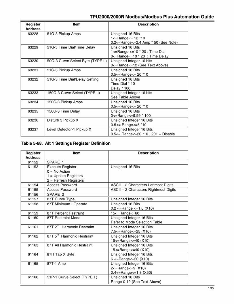
TPU2000/2000R Modbus/Modbus Plus Automation Guide
185
RegisterAddress
Item Description
63228 51G-3 Pickup Amps Unsigned 16 Bits1<=Range<= 12 *100.2<=Range<=2.4 Amp * 50 (See Note)
63229 51G-3 Time Dial/Time Delay Unsigned 16 Bits1<=Range <=10 * 20 : Time Dial0<=Range<=10 * 20 : Time Delay
63230 50G-3 Curve Select Byte (TYPE II) Unsigned Integer 16 bits0<=Range<=12 (See Text Above)
63231 51G-3 Pickup Amps Unsigned 16 Bits0.5<=Range<= 20 *10
63232 51G-3 Time Dial/Delay Setting Unsigned 16 BitsTime Dial * 10Delay * 100
63233 150G-3 Curve Select (TYPE II) Unsigned Integer 16 bitsSee Table Above
63234 150G-3 Pickup Amps Unsigned 16 Bits0.5<=Range<= 20 *10
63235 150G-3 Time Delay Unsigned 16 Bits0<=Range<=9.99 * 100
63236 Disturb 3 Pickup X Unsigned Integer 16 Bits0.5<= Range<=5 *10
63237 Level Detector-1 Pickup X Unsigned Integer 16 Bits0.5<= Range<=20 *10 , 201 = Disable
Table 5-68. Alt 1 Settings Register Definition
RegisterAddress
Item Description
61152 SPARE_161153 Execute Register
0 = No Action1 = Update Registers2 = Refresh Registers
Unsigned 16 Bits
61154 Access Password ASCII – 2 Characters Leftmost Digits61155 Access Password ASCII – 2 Characters Rightmost Digits61156 SPARE_261157 87T Curve Type Unsigned Integer 16 Bits61158 87T Minimum I Operate Unsigned 16 Bits
0.2 <=Range <=1.0 (X10)61159 87T Percent Restraint 15<=Range<=6061160 87T Restraint Mode Unsigned Integer 16 Bits
Refer to Mode Selection Table61161 87T 2nd Harmonic Restraint Unsigned Integer 16 Bits
7.5<=Range<=25 (X10)61162 87T 5th Harmonic Restraint Unsigned Integer 16 Bits
15<=Range<=40 (X10)61163 87T All Harmonic Restraint Unsigned Integer 16 Bits
15<=Range<=40 (X10)61164 87H Tap X Byte Unsigned Integer 16 Bits
6 <=Range<=20 (X10)61165 87T-1 Amp Unsigned Integer 16 Bits
2<=Range<=9 (X10)0.4<=Range<=1.8 (X50)
61166 51P-1 Curve Select (TYPE I ) Unsigned 16 BitsRange 0-12 (See Text Above)
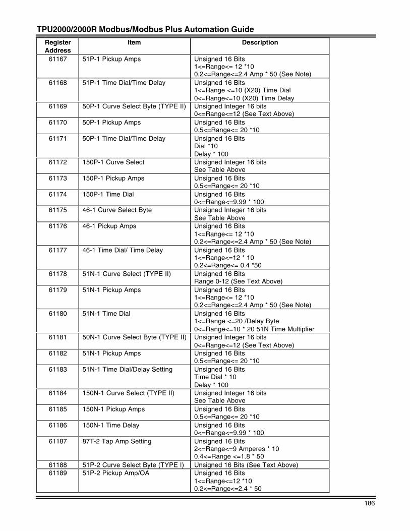
TPU2000/2000R Modbus/Modbus Plus Automation Guide
186
RegisterAddress
Item Description
61167 51P-1 Pickup Amps Unsigned 16 Bits1<=Range<= 12 *100.2<=Range<=2.4 Amp * 50 (See Note)
61168 51P-1 Time Dial/Time Delay Unsigned 16 Bits1<=Range <=10 (X20) Time Dial0<=Range<=10 (X20) Time Delay
61169 50P-1 Curve Select Byte (TYPE II) Unsigned Integer 16 bits0<=Range<=12 (See Text Above)
61170 50P-1 Pickup Amps Unsigned 16 Bits0.5<=Range<= 20 *10
61171 50P-1 Time Dial/Time Delay Unsigned 16 BitsDial *10Delay * 100
61172 150P-1 Curve Select Unsigned Integer 16 bitsSee Table Above
61173 150P-1 Pickup Amps Unsigned 16 Bits0.5<=Range<= 20 *10
61174 150P-1 Time Dial Unsigned 16 Bits0<=Range<=9.99 * 100
61175 46-1 Curve Select Byte Unsigned Integer 16 bitsSee Table Above
61176 46-1 Pickup Amps Unsigned 16 Bits1<=Range<= 12 *100.2<=Range<=2.4 Amp * 50 (See Note)
61177 46-1 Time Dial/ Time Delay Unsigned 16 Bits1<=Range<=12 * 100.2<=Range<= 0.4 *50
61178 51N-1 Curve Select (TYPE II) Unsigned 16 BitsRange 0-12 (See Text Above)
61179 51N-1 Pickup Amps Unsigned 16 Bits1<=Range<= 12 *100.2<=Range<=2.4 Amp * 50 (See Note)
61180 51N-1 Time Dial Unsigned 16 Bits1<=Range <=20 /Delay Byte0<=Range<=10 * 20 51N Time Multiplier
61181 50N-1 Curve Select Byte (TYPE II) Unsigned Integer 16 bits0<=Range<=12 (See Text Above)
61182 51N-1 Pickup Amps Unsigned 16 Bits0.5<=Range<= 20 *10
61183 51N-1 Time Dial/Delay Setting Unsigned 16 BitsTime Dial * 10Delay * 100
61184 150N-1 Curve Select (TYPE II) Unsigned Integer 16 bitsSee Table Above
61185 150N-1 Pickup Amps Unsigned 16 Bits0.5<=Range<= 20 *10
61186 150N-1 Time Delay Unsigned 16 Bits0<=Range<=9.99 * 100
61187 87T-2 Tap Amp Setting Unsigned 16 Bits2<=Range<=9 Amperes * 100.4<=Range <=1.8 * 50
61188 51P-2 Curve Select Byte (TYPE I) Unsigned 16 Bits (See Text Above)61189 51P-2 Pickup Amp/OA Unsigned 16 Bits
1<=Range<=12 *100.2<=Range<=2.4 * 50
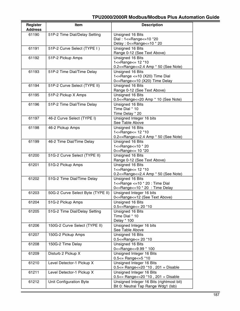
TPU2000/2000R Modbus/Modbus Plus Automation Guide
187
RegisterAddress
Item Description
61190 51P-2 Time Dial/Delay Setting Unsigned 16 BitsDial : 1<=Range<=10 *20Delay : 0<=Range<=10 * 20
61191 51P-2 Curve Select (TYPE I ) Unsigned 16 BitsRange 0-12 (See Text Above)
61192 51P-2 Pickup Amps Unsigned 16 Bits1<=Range<= 12 *100.2<=Range<=2.4 Amp * 50 (See Note)
61193 51P-2 Time Dial/Time Delay Unsigned 16 Bits1<=Range <=10 (X20) Time Dial0<=Range<=10 (X20) Time Delay
61194 51P-2 Curve Select (TYPE II) Unsigned 16 BitsRange 0-12 (See Text Above)
61195 51P-2 Pickup X Amps Unsigned 16 Bits0.5<=Range<=20 Amp * 10 (See Note)
61196 51P-2 Time Dial/Time Delay Unsigned 16 BitsTime Dial * 10Time Delay * 20
61197 46-2 Curve Select (TYPE I) Unsigned Integer 16 bitsSee Table Above
61198 46-2 Pickup Amps Unsigned 16 Bits1<=Range<= 12 *100.2<=Range<=2.4 Amp * 50 (See Note)
61199 46-2 Time Dial/Time Delay Unsigned 16 Bits1<=Range<=10 * 200<=Range<= 10 *20
61200 51G-2 Curve Select (TYPE II) Unsigned 16 BitsRange 0-12 (See Text Above)
61201 51G-2 Pickup Amps Unsigned 16 Bits1<=Range<= 12 *100.2<=Range<=2.4 Amp * 50 (See Note)
61202 51G-2 Time Dial/Time Delay Unsigned 16 Bits1<=Range <=10 * 20 : Time Dial0<=Range<=10 * 20 : Time Delay
61203 50G-2 Curve Select Byte (TYPE II) Unsigned Integer 16 bits0<=Range<=12 (See Text Above)
61204 51G-2 Pickup Amps Unsigned 16 Bits0.5<=Range<= 20 *10
61205 51G-2 Time Dial/Delay Setting Unsigned 16 BitsTime Dial * 10Delay * 100
61206 150G-2 Curve Select (TYPE II) Unsigned Integer 16 bitsSee Table Above
61207 150G-2 Pickup Amps Unsigned 16 Bits0.5<=Range<= 20 *10
61208 150G-2 Time Delay Unsigned 16 Bits0<=Range<=9.99 * 100
61209 Disturb 2 Pickup X Unsigned Integer 16 Bits0.5<= Range<=5 *10
61210 Level Detector-1 Pickup X Unsigned Integer 16 Bits0.5<= Range<=20 *10 , 201 = Disable
61211 Level Detector-1 Pickup X Unsigned Integer 16 Bits0.5<= Range<=20 *10 , 201 = Disable
61212 Unit Configuration Byte Unsigned Integer 16 Bits (rightmost bit)Bit 0: Neutral Tap Range Wdg1 (lsb)
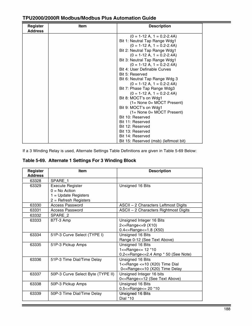
TPU2000/2000R Modbus/Modbus Plus Automation Guide
188
RegisterAddress
Item Description
(0 = 1-12 A, 1 = 0.2-2.4A)Bit 1: Neutral Tap Range Wdg1 (0 = 1-12 A, 1 = 0.2-2.4A)Bit 2: Neutral Tap Range Wdg1 (0 = 1-12 A, 1 = 0.2-2.4A)Bit 3: Neutral Tap Range Wdg1 (0 = 1-12 A, 1 = 0.2-2.4A)Bit 4: User Definable CurvesBit 5: ReservedBit 6: Neutral Tap Range Wdg 3 (0 = 1-12 A, 1 = 0.2-2.4A)Bit 7: Phase Tap Range Wdg3 (0 = 1-12 A, 1 = 0.2-2.4A)Bit 8: MOCT’s on Wdg1 (1= None 0= MOCT Present)Bit 9: MOCT’s on Wdg1 (1= None 0= MOCT Present)Bit 10: ReservedBit 11: ReservedBit 12: ReservedBit 13: ReservedBit 14: ReservedBit 15: Reserved (msb) (leftmost bit)
If a 3 Winding Relay is used, Alternate Settings Table Definitions are given in Table 5-69 Below:
Table 5-69. Alternate 1 Settings For 3 Winding Block
RegisterAddress
Item Description
63328 SPARE_163329 Execute Register
0 = No Action1 = Update Registers2 = Refresh Registers
Unsigned 16 Bits
63330 Access Password ASCII – 2 Characters Leftmost Digits63331 Access Password ASCII – 2 Characters Rightmost Digits63332 SPARE_263333 87T-3 Amp Unsigned Integer 16 Bits
2<=Range<=9 (X10)0.4<=Range<=1.8 (X50)
63334 51P-3 Curve Select (TYPE I) Unsigned 16 BitsRange 0-12 (See Text Above)
63335 51P-3 Pickup Amps Unsigned 16 Bits1<=Range<= 12 *100.2<=Range<=2.4 Amp * 50 (See Note)
63336 51P-3 Time Dial/Time Delay Unsigned 16 Bits1<=Range <=10 (X20) Time Dial 0<=Range<=10 (X20) Time Delay
63337 50P-3 Curve Select Byte (TYPE II) Unsigned Integer 16 bits0<=Range<=12 (See Text Above)
63338 50P-3 Pickup Amps Unsigned 16 Bits0.5<=Range<= 20 *10
63339 50P-3 Time Dial/Time Delay UUnnss iiggnneedd 1166 BBiittssDial *10
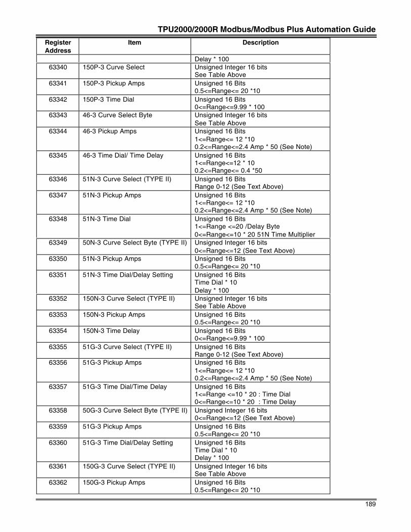
TPU2000/2000R Modbus/Modbus Plus Automation Guide
189
RegisterAddress
Item Description
Delay * 10063340 150P-3 Curve Select Unsigned Integer 16 bits
See Table Above63341 150P-3 Pickup Amps Unsigned 16 Bits
0.5<=Range<= 20 *1063342 150P-3 Time Dial Unsigned 16 Bits
0<=Range<=9.99 * 10063343 46-3 Curve Select Byte Unsigned Integer 16 bits
See Table Above63344 46-3 Pickup Amps Unsigned 16 Bits
1<=Range<= 12 *100.2<=Range<=2.4 Amp * 50 (See Note)
63345 46-3 Time Dial/ Time Delay Unsigned 16 Bits1<=Range<=12 * 100.2<=Range<= 0.4 *50
63346 51N-3 Curve Select (TYPE II) Unsigned 16 BitsRange 0-12 (See Text Above)
63347 51N-3 Pickup Amps Unsigned 16 Bits1<=Range<= 12 *100.2<=Range<=2.4 Amp * 50 (See Note)
63348 51N-3 Time Dial Unsigned 16 Bits1<=Range <=20 /Delay Byte0<=Range<=10 * 20 51N Time Multiplier
63349 50N-3 Curve Select Byte (TYPE II) Unsigned Integer 16 bits0<=Range<=12 (See Text Above)
63350 51N-3 Pickup Amps Unsigned 16 Bits0.5<=Range<= 20 *10
63351 51N-3 Time Dial/Delay Setting Unsigned 16 BitsTime Dial * 10Delay * 100
63352 150N-3 Curve Select (TYPE II) Unsigned Integer 16 bitsSee Table Above
63353 150N-3 Pickup Amps Unsigned 16 Bits0.5<=Range<= 20 *10
63354 150N-3 Time Delay Unsigned 16 Bits0<=Range<=9.99 * 100
63355 51G-3 Curve Select (TYPE II) Unsigned 16 BitsRange 0-12 (See Text Above)
63356 51G-3 Pickup Amps Unsigned 16 Bits1<=Range<= 12 *100.2<=Range<=2.4 Amp * 50 (See Note)
63357 51G-3 Time Dial/Time Delay Unsigned 16 Bits1<=Range <=10 * 20 : Time Dial0<=Range<=10 * 20 : Time Delay
63358 50G-3 Curve Select Byte (TYPE II) Unsigned Integer 16 bits0<=Range<=12 (See Text Above)
63359 51G-3 Pickup Amps Unsigned 16 Bits0.5<=Range<= 20 *10
63360 51G-3 Time Dial/Delay Setting Unsigned 16 BitsTime Dial * 10Delay * 100
63361 150G-3 Curve Select (TYPE II) Unsigned Integer 16 bitsSee Table Above
63362 150G-3 Pickup Amps Unsigned 16 Bits0.5<=Range<= 20 *10
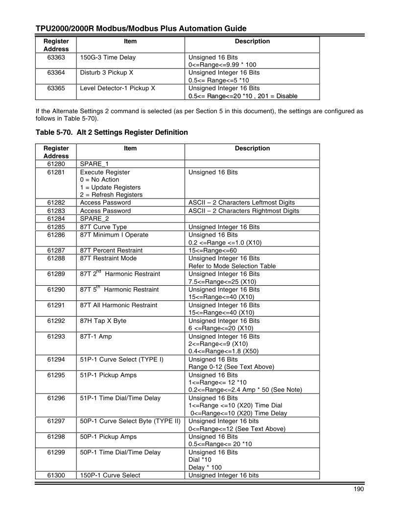
TPU2000/2000R Modbus/Modbus Plus Automation Guide
190
RegisterAddress
Item Description
63363 150G-3 Time Delay Unsigned 16 Bits0<=Range<=9.99 * 100
63364 Disturb 3 Pickup X Unsigned Integer 16 Bits0.5<= Range<=5 *10
63365 Level Detector-1 Pickup X Unsigned Integer 16 Bits00..55<<== RRaannggee<<==2200 **1100 ,, 220011 == DDiissaabbllee
If the Alternate Settings 2 command is selected (as per Section 5 in this document), the settings are configured asfollows in Table 5-70).
Table 5-70. Alt 2 Settings Register Definition
RegisterAddress
Item Description
61280 SPARE_161281 Execute Register
0 = No Action1 = Update Registers2 = Refresh Registers
Unsigned 16 Bits
61282 Access Password ASCII – 2 Characters Leftmost Digits61283 Access Password ASCII – 2 Characters Rightmost Digits61284 SPARE_261285 87T Curve Type Unsigned Integer 16 Bits61286 87T Minimum I Operate Unsigned 16 Bits
0.2 <=Range <=1.0 (X10)61287 87T Percent Restraint 15<=Range<=6061288 87T Restraint Mode Unsigned Integer 16 Bits
Refer to Mode Selection Table61289 87T 2nd Harmonic Restraint Unsigned Integer 16 Bits
7.5<=Range<=25 (X10)61290 87T 5th Harmonic Restraint Unsigned Integer 16 Bits
15<=Range<=40 (X10)61291 87T All Harmonic Restraint Unsigned Integer 16 Bits
15<=Range<=40 (X10)61292 87H Tap X Byte Unsigned Integer 16 Bits
6 <=Range<=20 (X10)61293 87T-1 Amp Unsigned Integer 16 Bits
2<=Range<=9 (X10)0.4<=Range<=1.8 (X50)
61294 51P-1 Curve Select (TYPE I) Unsigned 16 BitsRange 0-12 (See Text Above)
61295 51P-1 Pickup Amps Unsigned 16 Bits1<=Range<= 12 *100.2<=Range<=2.4 Amp * 50 (See Note)
61296 51P-1 Time Dial/Time Delay Unsigned 16 Bits1<=Range <=10 (X20) Time Dial 0<=Range<=10 (X20) Time Delay
61297 50P-1 Curve Select Byte (TYPE II) Unsigned Integer 16 bits0<=Range<=12 (See Text Above)
61298 50P-1 Pickup Amps Unsigned 16 Bits0.5<=Range<= 20 *10
61299 50P-1 Time Dial/Time Delay Unsigned 16 BitsDial *10Delay * 100
61300 150P-1 Curve Select Unsigned Integer 16 bits
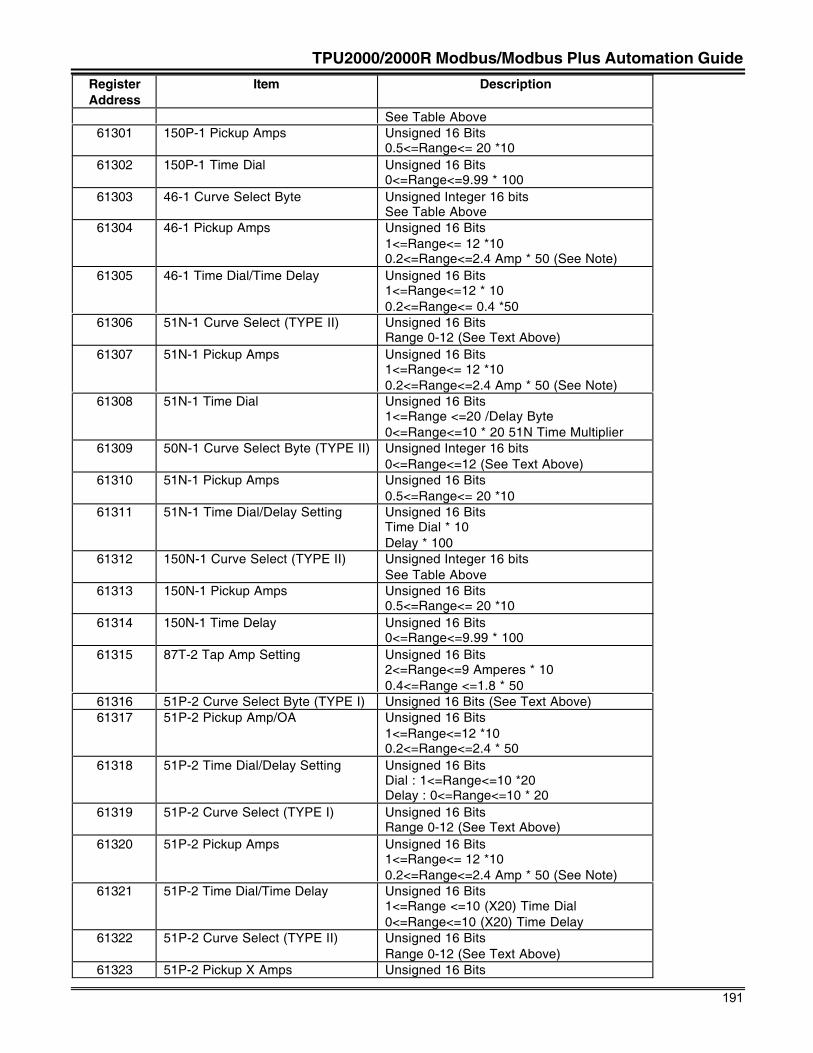
TPU2000/2000R Modbus/Modbus Plus Automation Guide
191
RegisterAddress
Item Description
See Table Above61301 150P-1 Pickup Amps Unsigned 16 Bits
0.5<=Range<= 20 *1061302 150P-1 Time Dial Unsigned 16 Bits
0<=Range<=9.99 * 10061303 46-1 Curve Select Byte Unsigned Integer 16 bits
See Table Above61304 46-1 Pickup Amps Unsigned 16 Bits
1<=Range<= 12 *100.2<=Range<=2.4 Amp * 50 (See Note)
61305 46-1 Time Dial/Time Delay Unsigned 16 Bits1<=Range<=12 * 100.2<=Range<= 0.4 *50
61306 51N-1 Curve Select (TYPE II) Unsigned 16 BitsRange 0-12 (See Text Above)
61307 51N-1 Pickup Amps Unsigned 16 Bits1<=Range<= 12 *100.2<=Range<=2.4 Amp * 50 (See Note)
61308 51N-1 Time Dial Unsigned 16 Bits1<=Range <=20 /Delay Byte0<=Range<=10 * 20 51N Time Multiplier
61309 50N-1 Curve Select Byte (TYPE II) Unsigned Integer 16 bits0<=Range<=12 (See Text Above)
61310 51N-1 Pickup Amps Unsigned 16 Bits0.5<=Range<= 20 *10
61311 51N-1 Time Dial/Delay Setting Unsigned 16 BitsTime Dial * 10Delay * 100
61312 150N-1 Curve Select (TYPE II) Unsigned Integer 16 bitsSee Table Above
61313 150N-1 Pickup Amps Unsigned 16 Bits0.5<=Range<= 20 *10
61314 150N-1 Time Delay Unsigned 16 Bits0<=Range<=9.99 * 100
61315 87T-2 Tap Amp Setting Unsigned 16 Bits2<=Range<=9 Amperes * 100.4<=Range <=1.8 * 50
61316 51P-2 Curve Select Byte (TYPE I) Unsigned 16 Bits (See Text Above)61317 51P-2 Pickup Amp/OA Unsigned 16 Bits
1<=Range<=12 *100.2<=Range<=2.4 * 50
61318 51P-2 Time Dial/Delay Setting Unsigned 16 BitsDial : 1<=Range<=10 *20Delay : 0<=Range<=10 * 20
61319 51P-2 Curve Select (TYPE I) Unsigned 16 BitsRange 0-12 (See Text Above)
61320 51P-2 Pickup Amps Unsigned 16 Bits1<=Range<= 12 *100.2<=Range<=2.4 Amp * 50 (See Note)
61321 51P-2 Time Dial/Time Delay Unsigned 16 Bits1<=Range <=10 (X20) Time Dial0<=Range<=10 (X20) Time Delay
61322 51P-2 Curve Select (TYPE II) Unsigned 16 BitsRange 0-12 (See Text Above)
61323 51P-2 Pickup X Amps Unsigned 16 Bits
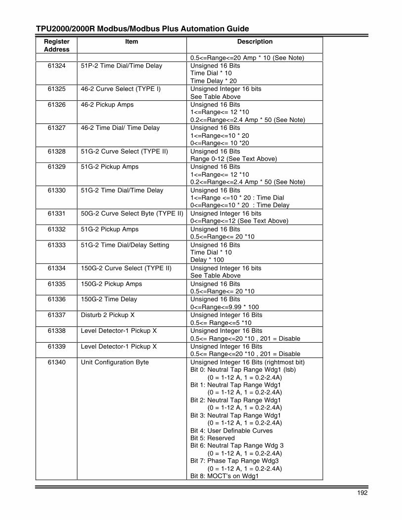
TPU2000/2000R Modbus/Modbus Plus Automation Guide
192
RegisterAddress
Item Description
0.5<=Range<=20 Amp * 10 (See Note)61324 51P-2 Time Dial/Time Delay Unsigned 16 Bits
Time Dial * 10Time Delay * 20
61325 46-2 Curve Select (TYPE I) Unsigned Integer 16 bitsSee Table Above
61326 46-2 Pickup Amps Unsigned 16 Bits1<=Range<= 12 *100.2<=Range<=2.4 Amp * 50 (See Note)
61327 46-2 Time Dial/ Time Delay Unsigned 16 Bits1<=Range<=10 * 200<=Range<= 10 *20
61328 51G-2 Curve Select (TYPE II) Unsigned 16 BitsRange 0-12 (See Text Above)
61329 51G-2 Pickup Amps Unsigned 16 Bits1<=Range<= 12 *100.2<=Range<=2.4 Amp * 50 (See Note)
61330 51G-2 Time Dial/Time Delay Unsigned 16 Bits1<=Range <=10 * 20 : Time Dial0<=Range<=10 * 20 : Time Delay
61331 50G-2 Curve Select Byte (TYPE II) Unsigned Integer 16 bits0<=Range<=12 (See Text Above)
61332 51G-2 Pickup Amps Unsigned 16 Bits0.5<=Range<= 20 *10
61333 51G-2 Time Dial/Delay Setting Unsigned 16 BitsTime Dial * 10Delay * 100
61334 150G-2 Curve Select (TYPE II) Unsigned Integer 16 bitsSee Table Above
61335 150G-2 Pickup Amps Unsigned 16 Bits0.5<=Range<= 20 *10
61336 150G-2 Time Delay Unsigned 16 Bits0<=Range<=9.99 * 100
61337 Disturb 2 Pickup X Unsigned Integer 16 Bits0.5<= Range<=5 *10
61338 Level Detector-1 Pickup X Unsigned Integer 16 Bits0.5<= Range<=20 *10 , 201 = Disable
61339 Level Detector-1 Pickup X Unsigned Integer 16 Bits0.5<= Range<=20 *10 , 201 = Disable
61340 Unit Configuration Byte Unsigned Integer 16 Bits (rightmost bit)Bit 0: Neutral Tap Range Wdg1 (lsb) (0 = 1-12 A, 1 = 0.2-2.4A)Bit 1: Neutral Tap Range Wdg1 (0 = 1-12 A, 1 = 0.2-2.4A)Bit 2: Neutral Tap Range Wdg1 (0 = 1-12 A, 1 = 0.2-2.4A)Bit 3: Neutral Tap Range Wdg1 (0 = 1-12 A, 1 = 0.2-2.4A)Bit 4: User Definable CurvesBit 5: ReservedBit 6: Neutral Tap Range Wdg 3 (0 = 1-12 A, 1 = 0.2-2.4A)Bit 7: Phase Tap Range Wdg3 (0 = 1-12 A, 1 = 0.2-2.4A)Bit 8: MOCT’s on Wdg1
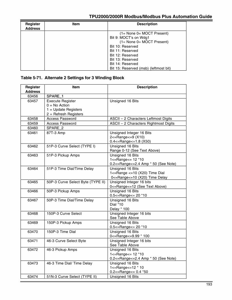
TPU2000/2000R Modbus/Modbus Plus Automation Guide
193
RegisterAddress
Item Description
(1= None 0= MOCT Present)Bit 9: MOCT’s on Wdg1 (1= None 0= MOCT Present)Bit 10: ReservedBit 11: ReservedBit 12: ReservedBit 13: ReservedBit 14: ReservedBit 15: Reserved (msb) (leftmost bit)
Table 5-71. Alternate 2 Settings for 3 Winding Block
RegisterAddress
Item Description
63456 SSPPAARREE__1163457 Execute Register
0 = No Action1 = Update Registers2 = Refresh Registers
Unsigned 16 Bits
63458 Access Password ASCII – 2 Characters Leftmost Digits63459 Access Password ASCII – 2 Characters Rightmost Digits63460 SPARE_263461 87T-3 Amp Unsigned Integer 16 Bits
2<=Range<=9 (X10)0.4<=Range<=1.8 (X50)
63462 51P-3 Curve Select (TYPE I) Unsigned 16 BitsRange 0-12 (See Text Above)
63463 51P-3 Pickup Amps Unsigned 16 Bits1<=Range<= 12 *100.2<=Range<=2.4 Amp * 50 (See Note)
63464 51P-3 Time Dial/Time Delay Unsigned 16 Bits1<=Range <=10 (X20) Time Dial 0<=Range<=10 (X20) Time Delay
63465 50P-3 Curve Select Byte (TYPE II) Unsigned Integer 16 bits0<=Range<=12 (See Text Above)
63466 50P-3 Pickup Amps Unsigned 16 Bits0.5<=Range<= 20 *10
63467 50P-3 Time Dial/Time Delay Unsigned 16 BitsDial *10Delay * 100
63468 150P-3 Curve Select Unsigned Integer 16 bitsSee Table Above
63469 150P-3 Pickup Amps Unsigned 16 Bits0.5<=Range<= 20 *10
63470 150P-3 Time Dial Unsigned 16 Bits0<=Range<=9.99 * 100
63471 46-3 Curve Select Byte Unsigned Integer 16 bitsSee Table Above
63472 46-3 Pickup Amps Unsigned 16 Bits1<=Range<= 12 *100.2<=Range<=2.4 Amp * 50 (See Note)
63473 46-3 Time Dial/ Time Delay Unsigned 16 Bits1<=Range<=12 * 100.2<=Range<= 0.4 *50
63474 51N-3 Curve Select (TYPE II) Unsigned 16 Bits
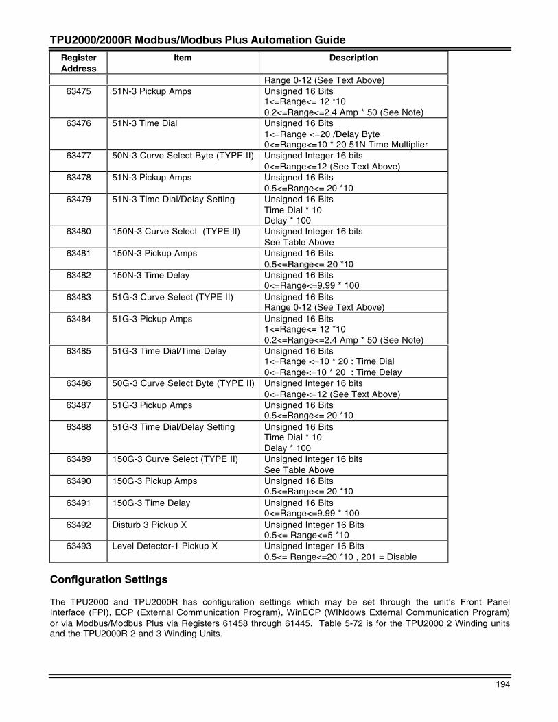
TPU2000/2000R Modbus/Modbus Plus Automation Guide
194
RegisterAddress
Item Description
Range 0-12 (See Text Above)63475 51N-3 Pickup Amps Unsigned 16 Bits
1<=Range<= 12 *100.2<=Range<=2.4 Amp * 50 (See Note)
63476 51N-3 Time Dial Unsigned 16 Bits1<=Range <=20 /Delay Byte0<=Range<=10 * 20 51N Time Multiplier
63477 50N-3 Curve Select Byte (TYPE II) Unsigned Integer 16 bits0<=Range<=12 (See Text Above)
63478 51N-3 Pickup Amps Unsigned 16 Bits0.5<=Range<= 20 *10
63479 51N-3 Time Dial/Delay Setting Unsigned 16 BitsTime Dial * 10Delay * 100
63480 150N-3 Curve Select (TYPE II) Unsigned Integer 16 bitsSee Table Above
63481 150N-3 Pickup Amps Unsigned 16 Bits00..55<<==RRaannggee<<== 2200 **1100
63482 150N-3 Time Delay Unsigned 16 Bits0<=Range<=9.99 * 100
63483 51G-3 Curve Select (TYPE II) Unsigned 16 BitsRange 0-12 (See Text Above)
63484 51G-3 Pickup Amps Unsigned 16 Bits1<=Range<= 12 *100.2<=Range<=2.4 Amp * 50 (See Note)
63485 51G-3 Time Dial/Time Delay Unsigned 16 Bits1<=Range <=10 * 20 : Time Dial0<=Range<=10 * 20 : Time Delay
63486 50G-3 Curve Select Byte (TYPE II) Unsigned Integer 16 bits0<=Range<=12 (See Text Above)
63487 51G-3 Pickup Amps Unsigned 16 Bits0.5<=Range<= 20 *10
63488 51G-3 Time Dial/Delay Setting Unsigned 16 BitsTime Dial * 10Delay * 100
63489 150G-3 Curve Select (TYPE II) Unsigned Integer 16 bitsSee Table Above
63490 150G-3 Pickup Amps Unsigned 16 Bits0.5<=Range<= 20 *10
63491 150G-3 Time Delay Unsigned 16 Bits0<=Range<=9.99 * 100
63492 Disturb 3 Pickup X Unsigned Integer 16 Bits0.5<= Range<=5 *10
63493 Level Detector-1 Pickup X Unsigned Integer 16 Bits0.5<= Range<=20 *10 , 201 = Disable
Configuration Settings
The TPU2000 and TPU2000R has configuration settings which may be set through the unit’s Front PanelInterface (FPI), ECP (External Communication Program), WinECP (WINdows External Communication Program)or via Modbus/Modbus Plus via Registers 61458 through 61445. Table 5-72 is for the TPU2000 2 Winding unitsand the TPU2000R 2 and 3 Winding Units.
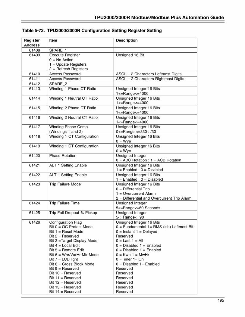
TPU2000/2000R Modbus/Modbus Plus Automation Guide
195
Table 5-72. TPU2000/2000R Configuration Setting Register Setting
RegisterAddress
Item Description
61408 SPARE_161409 Execute Register
0 = No Action1 = Update Registers2 = Refresh Registers
Unsigned 16 Bit
61410 Access Password ASCII – 2 Characters Leftmost Digits61411 Access Password ASCII – 2 Characters Rightmost Digits61412 SPARE_261413 Winding 1 Phase CT Ratio Unsigned Integer 16 Bits
1<=Range<=400061414 Winding 1 Neutral CT Ratio Unsigned Integer 16 Bits
1<=Range<=400061415 Winding 2 Phase CT Ratio Unsigned Integer 16 Bits
1<=Range<=400061416 Winding 2 Neutral CT Ratio Unsigned Integer 16 Bits
1<=Range<=400061417 Winding Phase Comp
(Windings 1 and 2)Unsigned Integer 16 Bits0<=Range <=330 : /30
61418 Winding 1 CT Configuration UUnnss iiggnneedd IInntteeggee rr 1166 BBiittss0 = Wye
61419 Winding 1 CT Configuration UUnnss iiggnneedd IInntteeggee rr 1166 BBiittss0 = Wye
61420 Phase Rotation Unsigned Integer0 = ABC Rotation : 1 = ACB Rotation
61421 ALT 1 Setting Enable Unsigned Integer 16 Bits1 = Enabled : 0 = Disabled
61422 ALT 1 Setting Enable Unsigned Integer 16 Bits1 = Enabled : 0 = Disabled
61423 Trip Failure Mode Unsigned Integer 16 Bits0 = Differential Trip1 = Overcurrent Alarm2 = Differential and Overcurrent Trip Alarm
61424 Trip Failure Time Unsigned Integer5<=Range<=60 Seconds
61425 Trip Fail Dropout % Pickup Unsigned Integer5<=Range<=90
61426 Configuration FlagBit 0 = OC Protect ModeBit 1 = Reset ModeBit 2 = ReservedBit 3 =Target Display ModeBit 4 = Local EditBit 5 = Remote EditBit 6 = Whr/VarHr Mtr ModeBit 7 = LCD lightBit 8 = Cross Block ModeBit 9 = ReservedBit 10 = ReservedBit 11 = ReservedBit 12 = ReservedBit 13 = ReservedBit 14 = Reserved
Unsigned Integer 16 Bits0 = Fundamental 1= RMS (lsb) Leftmost Bit0 = Instant 1 = DelayedReserved0 = Last 1 = All0 = Disabled 1 = Enabled0 = Disabled 1 = Enabled0 = Kwh 1 = MwHr0 =Timer 1= On0 = Disabled 1= EnabledReservedReservedReservedReservedReservedReserved
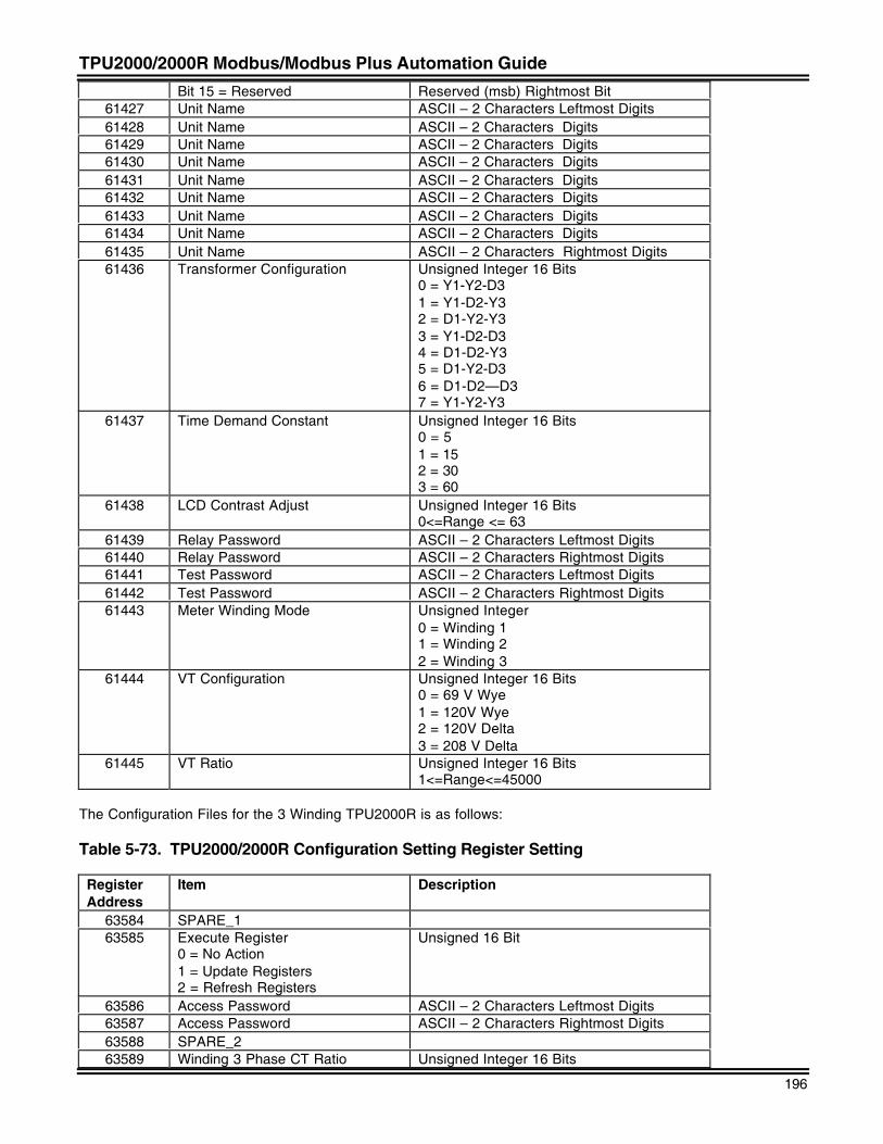
TPU2000/2000R Modbus/Modbus Plus Automation Guide
196
Bit 15 = Reserved Reserved (msb) Rightmost Bit61427 Unit Name ASCII – 2 Characters Leftmost Digits61428 Unit Name ASCII – 2 Characters Digits61429 Unit Name ASCII – 2 Characters Digits61430 Unit Name ASCII – 2 Characters Digits61431 Unit Name ASCII – 2 Characters Digits61432 Unit Name ASCII – 2 Characters Digits61433 Unit Name ASCII – 2 Characters Digits61434 Unit Name ASCII – 2 Characters Digits61435 Unit Name ASCII – 2 Characters Rightmost Digits61436 Transformer Configuration Unsigned Integer 16 Bits
0 = Y1-Y2-D31 = Y1-D2-Y32 = D1-Y2-Y33 = Y1-D2-D34 = D1-D2-Y35 = D1-Y2-D36 = D1-D2—D37 = Y1-Y2-Y3
61437 Time Demand Constant Unsigned Integer 16 Bits0 = 51 = 152 = 303 = 60
61438 LCD Contrast Adjust Unsigned Integer 16 Bits0<=Range <= 63
61439 Relay Password ASCII – 2 Characters Leftmost Digits61440 Relay Password ASCII – 2 Characters Rightmost Digits61441 Test Password ASCII – 2 Characters Leftmost Digits61442 Test Password ASCII – 2 Characters Rightmost Digits61443 Meter Winding Mode Unsigned Integer
0 = Winding 11 = Winding 22 = Winding 3
61444 VT Configuration Unsigned Integer 16 Bits0 = 69 V Wye1 = 120V Wye2 = 120V Delta3 = 208 V Delta
61445 VT Ratio Unsigned Integer 16 Bits1<=Range<=45000
The Configuration Files for the 3 Winding TPU2000R is as follows:
Table 5-73. TPU2000/2000R Configuration Setting Register Setting
RegisterAddress
Item Description
63584 SPARE_163585 Execute Register
0 = No Action1 = Update Registers2 = Refresh Registers
Unsigned 16 Bit
63586 Access Password ASCII – 2 Characters Leftmost Digits63587 Access Password ASCII – 2 Characters Rightmost Digits63588 SPARE_263589 Winding 3 Phase CT Ratio Unsigned Integer 16 Bits
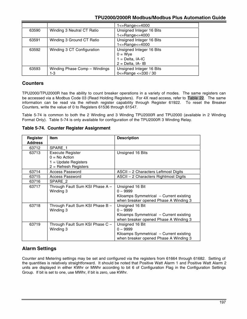
TPU2000/2000R Modbus/Modbus Plus Automation Guide
197
1<=Range<=400063590 Winding 3 Neutral CT Ratio Unsigned Integer 16 Bits
1<=Range<=400063591 Winding 3 Ground CT Ratio Unsigned Integer 16 Bits
1<=Range<=400063592 Winding 3 CT Configuration Unsigned Integer 16 Bits
0 = Wye1 = Delta, IA-IC2 = Delta, IA- IB
63593 Winding Phase Comp – Windings1-3
Unsigned Integer 16 Bits0<=Range <=330 / 30
Counters
TPU2000/TPU2000R has the ability to count breaker operations in a variety of modes. The same registers canbe accessed via a Modbus Code 03 (Read Holding Registers). For 4X read access, refer to Table 22. The sameinformation can be read via the refresh register capability through Register 61922. To reset the BreakerCounters, write the value of 0 to Registers 61536 through 61547.
Table 5-74 is common to both the 2 Winding and 3 Winding TPU2000R and TPU2000 (available in 2 WindingFormat Only). Table 5-74 is only available for configuration of the TPU2000R 3 Winding Relay.
Table 5-74. Counter Register Assignment
RegisterAddress
Item Description
63712 SPARE_163713 Execute Register
0 = No Action1 = Update Registers2 = Refresh Registers
Unsigned 16 Bits
63714 Access Password ASCII – 2 Characters Leftmost Digits63715 Access Password ASCII – 2 Characters Rightmost Digits63716 SPARE_263717 Through Fault Sum KSI Phase A –
Winding 3Unsigned 16 Bit0 – 9999Kiloamps Symmetrical – Current existingwhen breaker opened Phase A Winding 3
63718 Through Fault Sum KSI Phase B –Winding 3
Unsigned 16 Bit0 – 9999Kiloamps Symmetrical – Current existingwhen breaker opened Phase A Winding 3
63719 Through Fault Sum KSI Phase C –Winding 3
Unsigned 16 Bit0 – 9999Kiloamps Symmetrical – Current existingwhen breaker opened Phase A Winding 3
Alarm Settings
Counter and Metering settings may be set and configured via the registers from 61664 through 61682. Setting ofthe quantities is relatively straightforward. It should be noted that Positive Watt Alarm 1 and Positive Watt Alarm 2units are displayed in either KWhr or MWhr according to bit 6 of Configuration Flag in the Configuration SettingsGroup. If bit is set to one, use MWhr, if bit is zero, use KWhr.
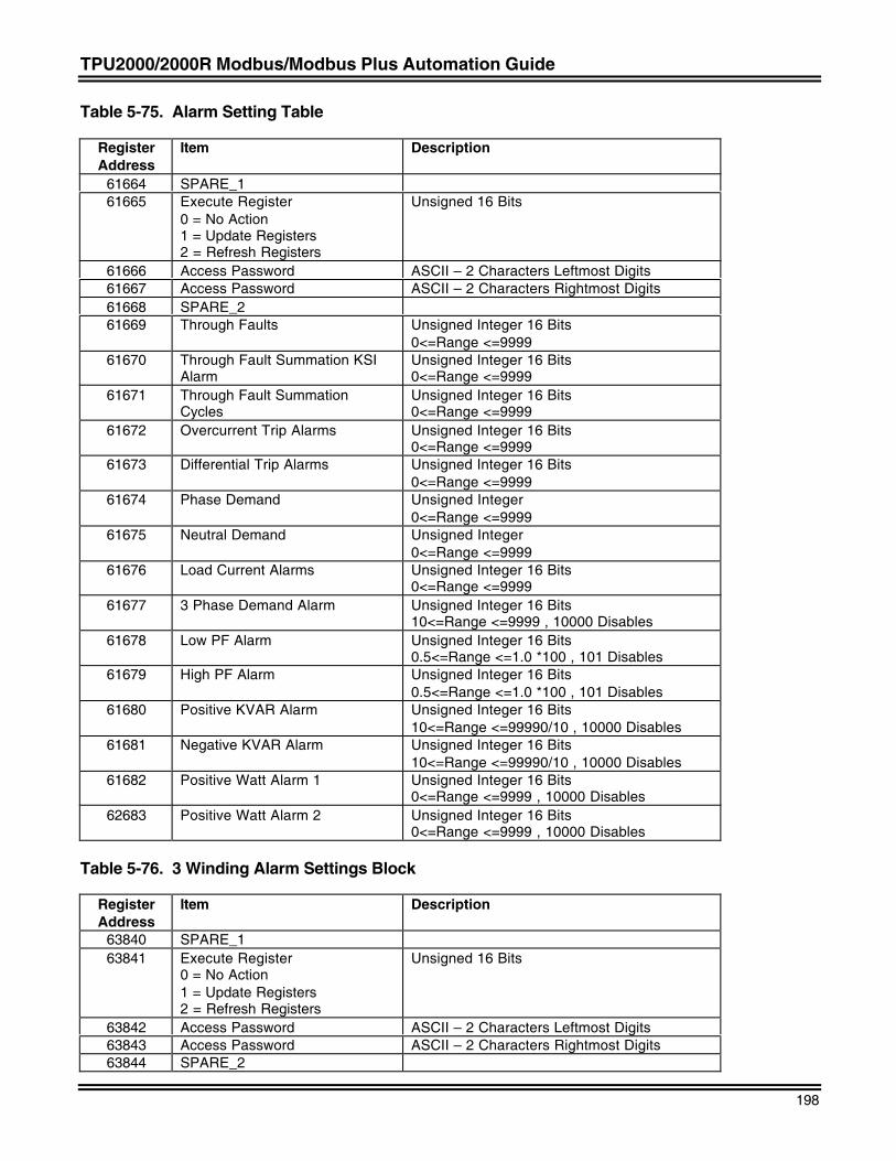
TPU2000/2000R Modbus/Modbus Plus Automation Guide
198
Table 5-75. Alarm Setting Table
RegisterAddress
Item Description
61664 SPARE_161665 Execute Register
0 = No Action1 = Update Registers2 = Refresh Registers
Unsigned 16 Bits
61666 Access Password ASCII – 2 Characters Leftmost Digits61667 Access Password ASCII – 2 Characters Rightmost Digits61668 SPARE_261669 Through Faults Unsigned Integer 16 Bits
0<=Range <=999961670 Through Fault Summation KSI
AlarmUnsigned Integer 16 Bits0<=Range <=9999
61671 Through Fault SummationCycles
Unsigned Integer 16 Bits0<=Range <=9999
61672 Overcurrent Trip Alarms Unsigned Integer 16 Bits0<=Range <=9999
61673 Differential Trip Alarms Unsigned Integer 16 Bits0<=Range <=9999
61674 Phase Demand Unsigned Integer0<=Range <=9999
61675 Neutral Demand Unsigned Integer0<=Range <=9999
61676 Load Current Alarms Unsigned Integer 16 Bits0<=Range <=9999
61677 3 Phase Demand Alarm Unsigned Integer 16 Bits10<=Range <=9999 , 10000 Disables
61678 Low PF Alarm Unsigned Integer 16 Bits0.5<=Range <=1.0 *100 , 101 Disables
61679 High PF Alarm Unsigned Integer 16 Bits0.5<=Range <=1.0 *100 , 101 Disables
61680 Positive KVAR Alarm Unsigned Integer 16 Bits10<=Range <=99990/10 , 10000 Disables
61681 Negative KVAR Alarm Unsigned Integer 16 Bits10<=Range <=99990/10 , 10000 Disables
61682 Positive Watt Alarm 1 Unsigned Integer 16 Bits0<=Range <=9999 , 10000 Disables
62683 Positive Watt Alarm 2 Unsigned Integer 16 Bits0<=Range <=9999 , 10000 Disables
Table 5-76. 3 Winding Alarm Settings Block
RegisterAddress
Item Description
63840 SPARE_163841 Execute Register
0 = No Action1 = Update Registers2 = Refresh Registers
Unsigned 16 Bits
63842 Access Password ASCII – 2 Characters Leftmost Digits63843 Access Password ASCII – 2 Characters Rightmost Digits63844 SPARE_2
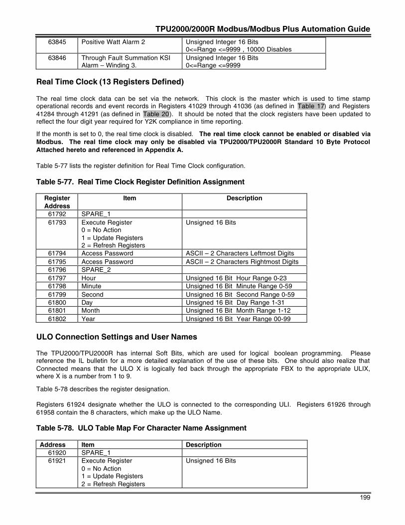
TPU2000/2000R Modbus/Modbus Plus Automation Guide
199
63845 Positive Watt Alarm 2 Unsigned Integer 16 Bits0<=Range <=9999 , 10000 Disables
63846 Through Fault Summation KSIAlarm – Winding 3.
Unsigned Integer 16 Bits0<=Range <=9999
Real Time Clock (13 Registers Defined)
The real time clock data can be set via the network. This clock is the master which is used to time stampoperational records and event records in Registers 41029 through 41036 (as defined in Table 17) and Registers41284 through 41291 (as defined in Table 20). It should be noted that the clock registers have been updated toreflect the four digit year required for Y2K compliance in time reporting.
If the month is set to 0, the real time clock is disabled. The real time clock cannot be enabled or disabled viaModbus. The real time clock may only be disabled via TPU2000/TPU2000R Standard 10 Byte ProtocolAttached hereto and referenced in Appendix A.
Table 5-77 lists the register definition for Real Time Clock configuration.
Table 5-77. Real Time Clock Register Definition Assignment
RegisterAddress
Item Description
61792 SPARE_161793 Execute Register
0 = No Action1 = Update Registers2 = Refresh Registers
Unsigned 16 Bits
61794 Access Password ASCII – 2 Characters Leftmost Digits61795 Access Password ASCII – 2 Characters Rightmost Digits61796 SPARE_261797 Hour Unsigned 16 Bit Hour Range 0-2361798 Minute Unsigned 16 Bit Minute Range 0-5961799 Second Unsigned 16 Bit Second Range 0-5961800 Day Unsigned 16 Bit Day Range 1-3161801 Month Unsigned 16 Bit Month Range 1-1261802 Year Unsigned 16 Bit Year Range 00-99
ULO Connection Settings and User Names
The TPU2000/TPU2000R has internal Soft Bits, which are used for logical boolean programming. Pleasereference the IL bulletin for a more detailed explanation of the use of these bits. One should also realize thatConnected means that the ULO X is logically fed back through the appropriate FBX to the appropriate ULIX,where X is a number from 1 to 9.
Table 5-78 describes the register designation.
Registers 61924 designate whether the ULO is connected to the corresponding ULI. Registers 61926 through61958 contain the 8 characters, which make up the ULO Name.
Table 5-78. ULO Table Map For Character Name Assignment
Address Item Description61920 SPARE_161921 Execute Register
0 = No Action1 = Update Registers2 = Refresh Registers
Unsigned 16 Bits
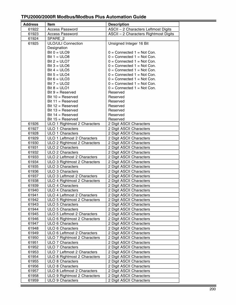
TPU2000/2000R Modbus/Modbus Plus Automation Guide
200
Address Item Description61922 Access Password ASCII – 2 Characters Leftmost Digits61923 Access Password ASCII – 2 Characters Rightmost Digits61924 SPARE_261925 ULO/ULI Connection
DesignationBit 0 = ULO9Bit 1 = ULO8Bit 2 = ULO7Bit 3 = ULO6Bit 4 = ULO5Bit 5 = ULO4Bit 6 = ULO3Bit 7 = ULO2Bit 8 = ULO1Bit 9 = ReservedBit 10 = ReservedBit 11 = ReservedBit 12 = ReservedBit 13 = ReservedBit 14 = ReservedBit 15 = Reserved
Unsigned Integer 16 Bit
0 = Connected 1 = Not Con.0 = Connected 1 = Not Con.0 = Connected 1 = Not Con.0 = Connected 1 = Not Con.0 = Connected 1 = Not Con.0 = Connected 1 = Not Con.0 = Connected 1 = Not Con.0 = Connected 1 = Not Con.0 = Connected 1 = Not Con.ReservedReservedReservedReservedReservedReservedReserved
61926 ULO 1 Rightmost 2 Characters 2 Digit ASCII Characters61927 ULO 1 Characters 2 Digit ASCII Characters61928 ULO 1 Characters 2 Digit ASCII Characters61929 ULO 1 Leftmost 2 Characters 2 Digit ASCII Characters61930 ULO 2 Rightmost 2 Characters 2 Digit ASCII Characters61931 ULO 2 Characters 2 Digit ASCII Characters61932 ULO 2 Characters 2 Digit ASCII Characters61933 ULO 2 Leftmost 2 Characters 2 Digit ASCII Characters61934 ULO 3 Rightmost 2 Characters 2 Digit ASCII Characters61935 ULO 3 Characters 2 Digit ASCII Characters61936 ULO 3 Characters 2 Digit ASCII Characters61937 ULO 3 Leftmost 2 Characters 2 Digit ASCII Characters61938 ULO 4 Rightmost 2 Characters 2 Digit ASCII Characters61939 ULO 4 Characters 2 Digit ASCII Characters61940 ULO 4 Characters 2 Digit ASCII Characters61941 ULO 4 Leftmost 2 Characters 2 Digit ASCII Characters61942 ULO 5 Rightmost 2 Characters 2 Digit ASCII Characters61943 ULO 5 Characters 2 Digit ASCII Characters61944 ULO 5 Characters 2 Digit ASCII Characters61945 ULO 5 Leftmost 2 Characters 2 Digit ASCII Characters61946 ULO 6 Rightmost 2 Characters 2 Digit ASCII Characters61947 ULO 6 Characters 2 Digit ASCII Characters61948 ULO 6 Characters 2 Digit ASCII Characters61949 ULO 6 Leftmost 2 Characters 2 Digit ASCII Characters61950 ULO 7 Rightmost 2 Characters 2 Digit ASCII Characters61951 ULO 7 Characters 2 Digit ASCII Characters61952 ULO 7 Characters 2 Digit ASCII Characters61953 ULO 7 Leftmost 2 Characters 2 Digit ASCII Characters61954 ULO 8 Rightmost 2 Characters 2 Digit ASCII Characters61955 ULO 8 Characters 2 Digit ASCII Characters61956 ULO 8 Characters 2 Digit ASCII Characters61957 ULO 8 Leftmost 2 Characters 2 Digit ASCII Characters61958 ULO 9 Rightmost 2 Characters 2 Digit ASCII Characters61959 ULO 9 Characters 2 Digit ASCII Characters
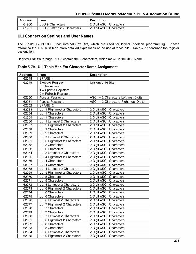
TPU2000/2000R Modbus/Modbus Plus Automation Guide
201
Address Item Description61960 ULO 9 Characters 2 Digit ASCII Characters61961 ULO 9 Leftmost 2 Characters 2 Digit ASCII Characters
ULI Connection Settings and User Names
The TPU2000/TPU2000R has internal Soft Bits, which are used for logical boolean programming. Pleasereference the IL bulletin for a more detailed explanation of the use of these bits. Table 5-79 describes the registerdesignation.
Registers 61926 through 61958 contain the 8 characters, which make up the ULO Name.
Table 5-79. ULI Table Map For Character Name Assignment
Address Item Description62048 SPARE_162049 Execute Register
0 = No Action1 = Update Registers2 = Refresh Registers
Unsigned 16 Bits
62050 Access Password ASCII – 2 Characters Leftmost Digits62051 Access Password ASCII – 2 Characters Rightmost Digits62052 SPARE_262053 ULI 1 Rightmost 2 Characters 2 Digit ASCII Characters62054 ULI 1 Characters 2 Digit ASCII Characters62055 ULI 1 Characters 2 Digit ASCII Characters62056 ULI 1 Leftmost 2 Characters 2 Digit ASCII Characters62057 ULI 2 Rightmost 2 Characters 2 Digit ASCII Characters62058 ULI 2 Characters 2 Digit ASCII Characters62059 ULI 2 Characters 2 Digit ASCII Characters62060 ULI 2 Leftmost 2 Characters 2 Digit ASCII Characters62061 ULI 3 Rightmost 2 Characters 2 Digit ASCII Characters62062 ULI 3 Characters 2 Digit ASCII Characters62063 ULI 3 Characters 2 Digit ASCII Characters62064 ULI 3 Leftmost 2 Characters 2 Digit ASCII Characters62065 ULI 4 Rightmost 2 Characters 2 Digit ASCII Characters62066 ULI 4 Characters 2 Digit ASCII Characters62067 ULI 4 Characters 2 Digit ASCII Characters62068 ULI 4 Leftmost 2 Characters 2 Digit ASCII Characters62069 ULI 5 Rightmost 2 Characters 2 Digit ASCII Characters62070 ULI 5 Characters 2 Digit ASCII Characters62071 ULI 5 Characters 2 Digit ASCII Characters62072 ULI 5 Leftmost 2 Characters 2 Digit ASCII Characters62073 ULI 6 Rightmost 2 Characters 2 Digit ASCII Characters62074 ULI 6 Characters 2 Digit ASCII Characters62075 ULI 6 Characters 2 Digit ASCII Characters62076 ULI 6 Leftmost 2 Characters 2 Digit ASCII Characters62077 ULI 7 Rightmost 2 Characters 2 Digit ASCII Characters62078 ULI 7 Characters 2 Digit ASCII Characters62079 ULI 7 Characters 2 Digit ASCII Characters62080 ULI 7 Leftmost 2 Characters 2 Digit ASCII Characters62081 ULI 8 Rightmost 2 Characters 2 Digit ASCII Characters62082 ULI 8 Characters 2 Digit ASCII Characters62083 ULI 8 Characters 2 Digit ASCII Characters62084 ULI 8 Leftmost 2 Characters 2 Digit ASCII Characters62085 ULI 9 Rightmost 2 Characters 2 Digit ASCII Characters
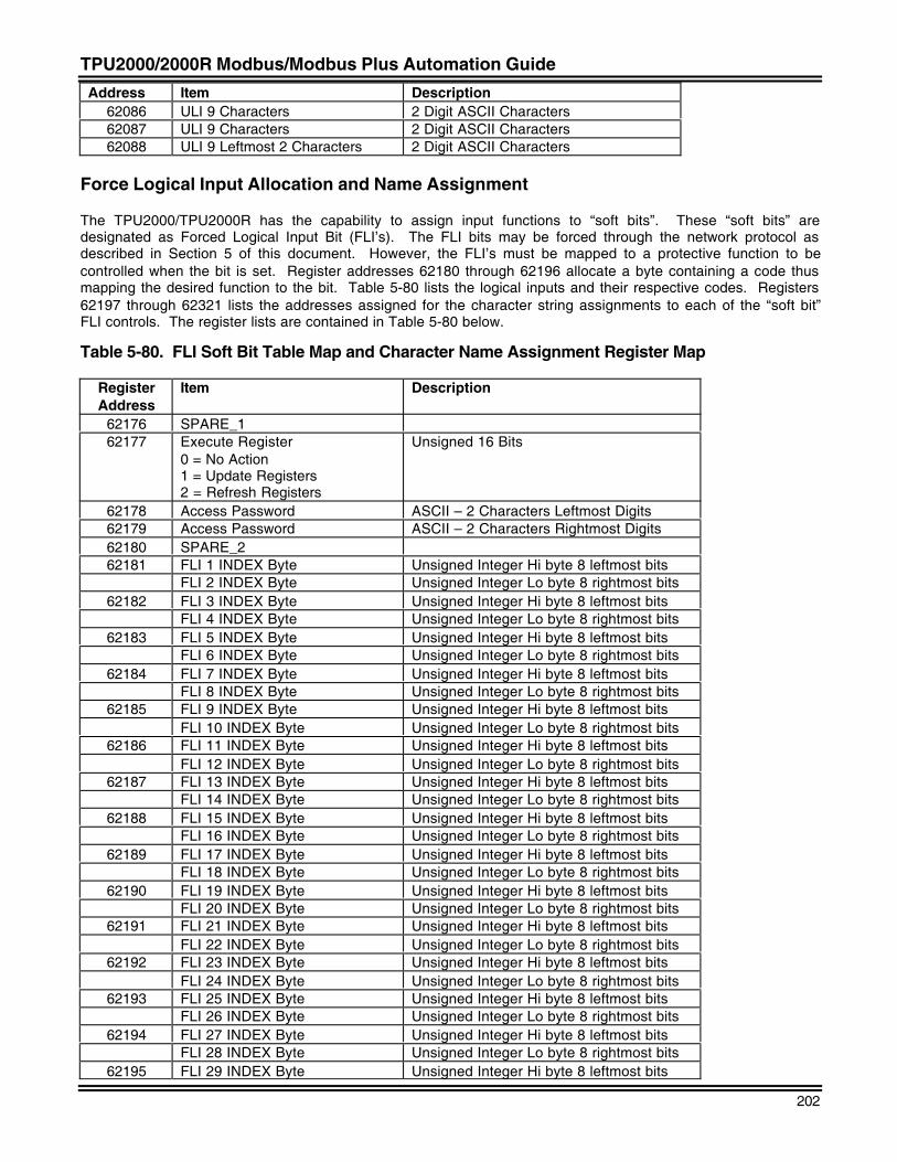
TPU2000/2000R Modbus/Modbus Plus Automation Guide
202
Address Item Description62086 ULI 9 Characters 2 Digit ASCII Characters62087 ULI 9 Characters 2 Digit ASCII Characters62088 ULI 9 Leftmost 2 Characters 2 Digit ASCII Characters
Force Logical Input Allocation and Name Assignment
The TPU2000/TPU2000R has the capability to assign input functions to “soft bits”. These “soft bits” aredesignated as Forced Logical Input Bit (FLI’s). The FLI bits may be forced through the network protocol asdescribed in Section 5 of this document. However, the FLI’s must be mapped to a protective function to becontrolled when the bit is set. Register addresses 62180 through 62196 allocate a byte containing a code thusmapping the desired function to the bit. Table 5-80 lists the logical inputs and their respective codes. Registers62197 through 62321 lists the addresses assigned for the character string assignments to each of the “soft bit”FLI controls. The register lists are contained in Table 5-80 below.
Table 5-80. FLI Soft Bit Table Map and Character Name Assignment Register Map
RegisterAddress
Item Description
62176 SPARE_162177 Execute Register
0 = No Action1 = Update Registers2 = Refresh Registers
Unsigned 16 Bits
62178 Access Password ASCII – 2 Characters Leftmost Digits62179 Access Password ASCII – 2 Characters Rightmost Digits62180 SPARE_262181 FLI 1 INDEX Byte Unsigned Integer Hi byte 8 leftmost bits
FLI 2 INDEX Byte Unsigned Integer Lo byte 8 rightmost bits62182 FLI 3 INDEX Byte Unsigned Integer Hi byte 8 leftmost bits
FLI 4 INDEX Byte Unsigned Integer Lo byte 8 rightmost bits62183 FLI 5 INDEX Byte Unsigned Integer Hi byte 8 leftmost bits
FLI 6 INDEX Byte Unsigned Integer Lo byte 8 rightmost bits62184 FLI 7 INDEX Byte Unsigned Integer Hi byte 8 leftmost bits
FLI 8 INDEX Byte Unsigned Integer Lo byte 8 rightmost bits62185 FLI 9 INDEX Byte Unsigned Integer Hi byte 8 leftmost bits
FLI 10 INDEX Byte Unsigned Integer Lo byte 8 rightmost bits62186 FLI 11 INDEX Byte Unsigned Integer Hi byte 8 leftmost bits
FLI 12 INDEX Byte Unsigned Integer Lo byte 8 rightmost bits62187 FLI 13 INDEX Byte Unsigned Integer Hi byte 8 leftmost bits
FLI 14 INDEX Byte Unsigned Integer Lo byte 8 rightmost bits62188 FLI 15 INDEX Byte Unsigned Integer Hi byte 8 leftmost bits
FLI 16 INDEX Byte Unsigned Integer Lo byte 8 rightmost bits62189 FLI 17 INDEX Byte Unsigned Integer Hi byte 8 leftmost bits
FLI 18 INDEX Byte Unsigned Integer Lo byte 8 rightmost bits62190 FLI 19 INDEX Byte Unsigned Integer Hi byte 8 leftmost bits
FLI 20 INDEX Byte Unsigned Integer Lo byte 8 rightmost bits62191 FLI 21 INDEX Byte Unsigned Integer Hi byte 8 leftmost bits
FLI 22 INDEX Byte Unsigned Integer Lo byte 8 rightmost bits62192 FLI 23 INDEX Byte Unsigned Integer Hi byte 8 leftmost bits
FLI 24 INDEX Byte Unsigned Integer Lo byte 8 rightmost bits62193 FLI 25 INDEX Byte Unsigned Integer Hi byte 8 leftmost bits
FLI 26 INDEX Byte Unsigned Integer Lo byte 8 rightmost bits62194 FLI 27 INDEX Byte Unsigned Integer Hi byte 8 leftmost bits
FLI 28 INDEX Byte Unsigned Integer Lo byte 8 rightmost bits62195 FLI 29 INDEX Byte Unsigned Integer Hi byte 8 leftmost bits
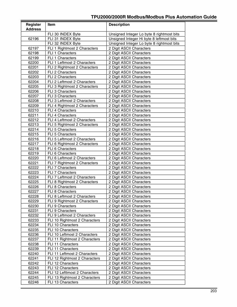
TPU2000/2000R Modbus/Modbus Plus Automation Guide
203
RegisterAddress
Item Description
FLI 30 INDEX Byte Unsigned Integer Lo byte 8 rightmost bits62196 FLI 31 INDEX Byte Unsigned Integer Hi byte 8 leftmost bits
FLI 32 INDEX Byte Unsigned Integer Lo byte 8 rightmost bits62197 FLI 1 Rightmost 2 Characters 2 Digit ASCII Characters62198 FLI 1 Characters 2 Digit ASCII Characters62199 FLI 1 Characters 2 Digit ASCII Characters62200 FLI 1 Leftmost 2 Characters 2 Digit ASCII Characters62201 FLI 2 Rightmost 2 Characters 2 Digit ASCII Characters62202 FLI 2 Characters 2 Digit ASCII Characters62203 FLI 2 Characters 2 Digit ASCII Characters62204 FLI 2 Leftmost 2 Characters 2 Digit ASCII Characters62205 FLI 3 Rightmost 2 Characters 2 Digit ASCII Characters62206 FLI 3 Characters 2 Digit ASCII Characters62207 FLI 3 Characters 2 Digit ASCII Characters62208 FLI 3 Leftmost 2 Characters 2 Digit ASCII Characters62209 FLI 4 Rightmost 2 Characters 2 Digit ASCII Characters62210 FLI 4 Characters 2 Digit ASCII Characters62211 FLI 4 Characters 2 Digit ASCII Characters62212 FLI 4 Leftmost 2 Characters 2 Digit ASCII Characters62213 FLI 5 Rightmost 2 Characters 2 Digit ASCII Characters62214 FLI 5 Characters 2 Digit ASCII Characters62215 FLI 5 Characters 2 Digit ASCII Characters62216 FLI 5 Leftmost 2 Characters 2 Digit ASCII Characters62217 FLI 6 Rightmost 2 Characters 2 Digit ASCII Characters62218 FLI 6 Characters 2 Digit ASCII Characters62219 FLI 6 Characters 2 Digit ASCII Characters62220 FLI 6 Leftmost 2 Characters 2 Digit ASCII Characters62221 FLI 7 Rightmost 2 Characters 2 Digit ASCII Characters62222 FLI 7 Characters 2 Digit ASCII Characters62223 FLI 7 Characters 2 Digit ASCII Characters62224 FLI 7 Leftmost 2 Characters 2 Digit ASCII Characters62225 FLI 8 Rightmost 2 Characters 2 Digit ASCII Characters62226 FLI 8 Characters 2 Digit ASCII Characters62227 FLI 8 Characters 2 Digit ASCII Characters62228 FLI 8 Leftmost 2 Characters 2 Digit ASCII Characters62229 FLI 9 Rightmost 2 Characters 2 Digit ASCII Characters62230 FLI 9 Characters 2 Digit ASCII Characters62231 FLI 9 Characters 2 Digit ASCII Characters62232 FLI 9 Leftmost 2 Characters 2 Digit ASCII Characters62233 FLI 10 Rightmost 2 Characters 2 Digit ASCII Characters62234 FLI 10 Characters 2 Digit ASCII Characters62235 FLI 10 Characters 2 Digit ASCII Characters62236 FLI 10 Leftmost 2 Characters 2 Digit ASCII Characters62237 FLI 11 Rightmost 2 Characters 2 Digit ASCII Characters62238 FLI 11 Characters 2 Digit ASCII Characters62239 FLI 11 Characters 2 Digit ASCII Characters62240 FLI 11 Leftmost 2 Characters 2 Digit ASCII Characters62241 FLI 12 Rightmost 2 Characters 2 Digit ASCII Characters62242 FLI 12 Characters 2 Digit ASCII Characters62243 FLI 12 Characters 2 Digit ASCII Characters62244 FLI 12 Lefttmost 2 Characters 2 Digit ASCII Characters62245 FLI 13 Rightmost 2 Characters 2 Digit ASCII Characters62246 FLI 13 Characters 2 Digit ASCII Characters
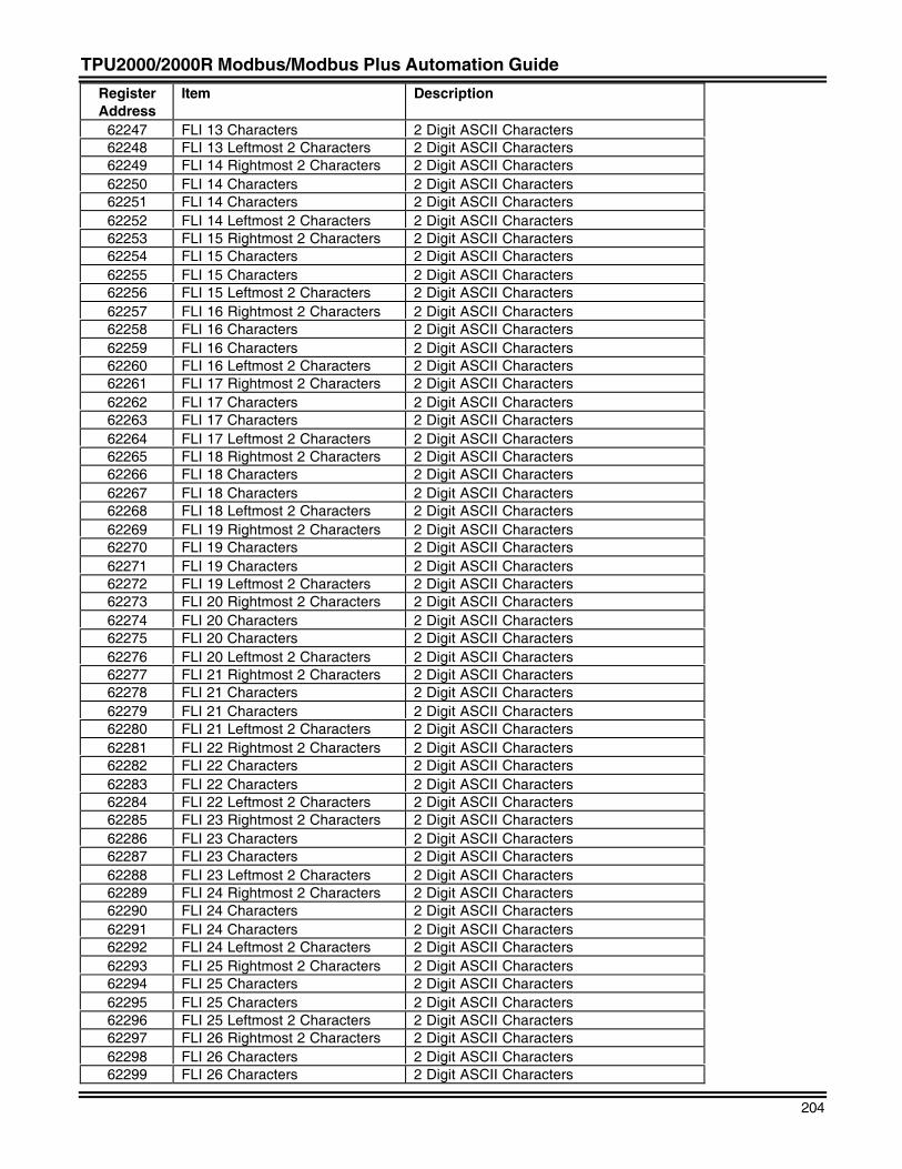
TPU2000/2000R Modbus/Modbus Plus Automation Guide
204
RegisterAddress
Item Description
62247 FLI 13 Characters 2 Digit ASCII Characters62248 FLI 13 Leftmost 2 Characters 2 Digit ASCII Characters62249 FLI 14 Rightmost 2 Characters 2 Digit ASCII Characters62250 FLI 14 Characters 2 Digit ASCII Characters62251 FLI 14 Characters 2 Digit ASCII Characters62252 FLI 14 Leftmost 2 Characters 2 Digit ASCII Characters62253 FLI 15 Rightmost 2 Characters 2 Digit ASCII Characters62254 FLI 15 Characters 2 Digit ASCII Characters62255 FLI 15 Characters 2 Digit ASCII Characters62256 FLI 15 Leftmost 2 Characters 2 Digit ASCII Characters62257 FLI 16 Rightmost 2 Characters 2 Digit ASCII Characters62258 FLI 16 Characters 2 Digit ASCII Characters62259 FLI 16 Characters 2 Digit ASCII Characters62260 FLI 16 Leftmost 2 Characters 2 Digit ASCII Characters62261 FLI 17 Rightmost 2 Characters 2 Digit ASCII Characters62262 FLI 17 Characters 2 Digit ASCII Characters62263 FLI 17 Characters 2 Digit ASCII Characters62264 FLI 17 Leftmost 2 Characters 2 Digit ASCII Characters62265 FLI 18 Rightmost 2 Characters 2 Digit ASCII Characters62266 FLI 18 Characters 2 Digit ASCII Characters62267 FLI 18 Characters 2 Digit ASCII Characters62268 FLI 18 Leftmost 2 Characters 2 Digit ASCII Characters62269 FLI 19 Rightmost 2 Characters 2 Digit ASCII Characters62270 FLI 19 Characters 2 Digit ASCII Characters62271 FLI 19 Characters 2 Digit ASCII Characters62272 FLI 19 Leftmost 2 Characters 2 Digit ASCII Characters62273 FLI 20 Rightmost 2 Characters 2 Digit ASCII Characters62274 FLI 20 Characters 2 Digit ASCII Characters62275 FLI 20 Characters 2 Digit ASCII Characters62276 FLI 20 Leftmost 2 Characters 2 Digit ASCII Characters62277 FLI 21 Rightmost 2 Characters 2 Digit ASCII Characters62278 FLI 21 Characters 2 Digit ASCII Characters62279 FLI 21 Characters 2 Digit ASCII Characters62280 FLI 21 Leftmost 2 Characters 2 Digit ASCII Characters62281 FLI 22 Rightmost 2 Characters 2 Digit ASCII Characters62282 FLI 22 Characters 2 Digit ASCII Characters62283 FLI 22 Characters 2 Digit ASCII Characters62284 FLI 22 Leftmost 2 Characters 2 Digit ASCII Characters62285 FLI 23 Rightmost 2 Characters 2 Digit ASCII Characters62286 FLI 23 Characters 2 Digit ASCII Characters62287 FLI 23 Characters 2 Digit ASCII Characters62288 FLI 23 Leftmost 2 Characters 2 Digit ASCII Characters62289 FLI 24 Rightmost 2 Characters 2 Digit ASCII Characters62290 FLI 24 Characters 2 Digit ASCII Characters62291 FLI 24 Characters 2 Digit ASCII Characters62292 FLI 24 Leftmost 2 Characters 2 Digit ASCII Characters62293 FLI 25 Rightmost 2 Characters 2 Digit ASCII Characters62294 FLI 25 Characters 2 Digit ASCII Characters62295 FLI 25 Characters 2 Digit ASCII Characters62296 FLI 25 Leftmost 2 Characters 2 Digit ASCII Characters62297 FLI 26 Rightmost 2 Characters 2 Digit ASCII Characters62298 FLI 26 Characters 2 Digit ASCII Characters62299 FLI 26 Characters 2 Digit ASCII Characters
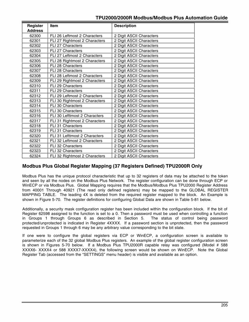
TPU2000/2000R Modbus/Modbus Plus Automation Guide
205
RegisterAddress
Item Description
62300 FLI 26 Leftmost 2 Characters 2 Digit ASCII Characters62301 FLI 27 Rightmost 2 Characters 2 Digit ASCII Characters62302 FLI 27 Characters 2 Digit ASCII Characters62303 FLI 27 Characters 2 Digit ASCII Characters62304 FLI 27 Leftmost 2 Characters 2 Digit ASCII Characters62305 FLI 28 Rightmost 2 Characters 2 Digit ASCII Characters62306 FLI 28 Characters 2 Digit ASCII Characters62307 FLI 28 Characters 2 Digit ASCII Characters62308 FLI 28 Leftmost 2 Characters 2 Digit ASCII Characters62309 FLI 29 Rightmost 2 Characters 2 Digit ASCII Characters62310 FLI 29 Characters 2 Digit ASCII Characters62311 FLI 29 Characters 2 Digit ASCII Characters62312 FLI 29 Leftmost 2 Characters 2 Digit ASCII Characters62313 FLI 30 Rightmost 2 Characters 2 Digit ASCII Characters62314 FLI 30 Characters 2 Digit ASCII Characters62315 FLI 30 Characters 2 Digit ASCII Characters62316 FLI 30 Lefttmost 2 Characters 2 Digit ASCII Characters62317 FLI 31 Rightmost 2 Characters 2 Digit ASCII Characters62318 FLI 31 Characters 2 Digit ASCII Characters62319 FLI 31 Characters 2 Digit ASCII Characters62320 FLI 31 Lefttmost 2 Characters 2 Digit ASCII Characters62321 FLI 32 Leftmost 2 Characters 2 Digit ASCII Characters62322 FLI 32 Characters 2 Digit ASCII Characters62323 FLI 32 Characters 2 Digit ASCII Characters62324 FLI 32 Rightmost 2 Characters 2 Digit ASCII Characters
Modbus Plus Global Register Mapping (37 Registers Defined) TPU2000R Only
Modbus Plus has the unique protocol characteristic that up to 32 registers of data may be attached to the tokenand seen by all the nodes on the Modbus Plus Network. The register configuration can be done through ECP orWinECP or via Modbus Plus. Global Mapping requires that the Modbus/Modbus Plus TPU2000 Register Addressfrom 40001 Through 40921 (The read only defined registers) may be mapped to the GLOBAL REGISTERMAPPING TABLE. The leading 4X is deleted from the required register mapped to the block. An Example isshown in Figure 5-70. The register definitions for configuring Global Data are shown in Table 5-81 below.
Additionally, a security mask configuration register has been included within the configuration block. If the bit ofRegister 62598 assigned to the function is set to a 0. Then a password must be used when controlling a functionin Groups 1 through Groups 6 as described in Section 5. The status of control being passwordprotected/unprotected is indicated in Register 4XXXX. If a password section is unprotected, then the passwordrequested in Groups 1 through 6 may be any arbitrary value corresponding to the bit state.
If one were to configure the global registers via ECP or WinECP, a configuration screen is available toparameterize each of the 32 global Modbus Plus registers. An example of the global register configuration screenis shown in Figures 5-70 below. If a Modbus Plus TPU2000R capable relay was configured (Model # 588XXXX6- XXXX4 or 588 XXXX7-XXXX4), the following screen would be shown on WinECP. Note the GlobalRegister Tab (accessed from the “SETTINGS” menu header) is visible and available as an option.
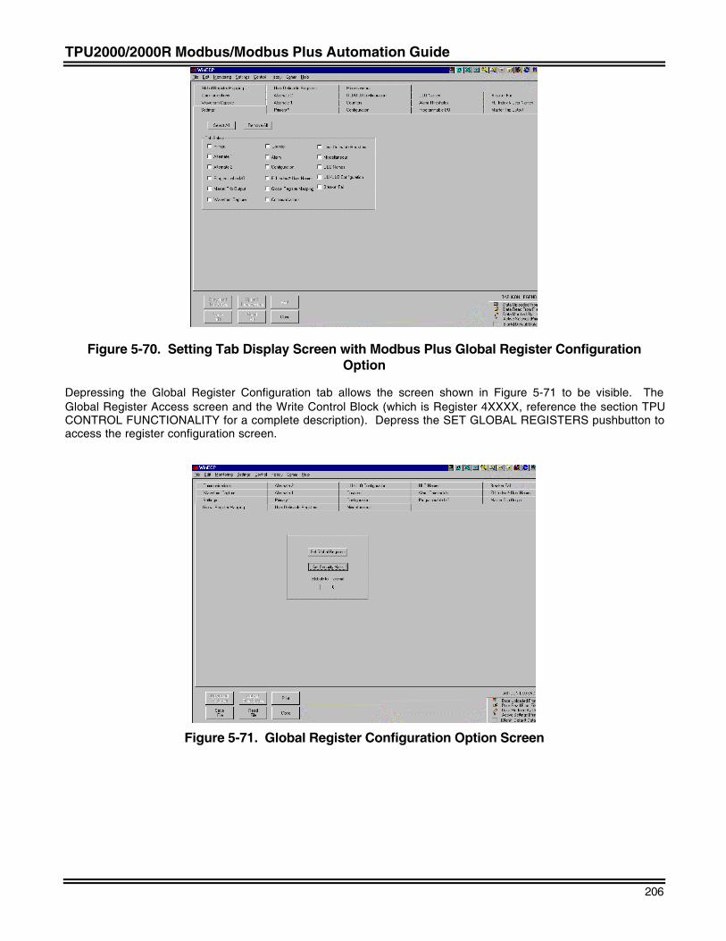
TPU2000/2000R Modbus/Modbus Plus Automation Guide
206
Figure 5-70. Setting Tab Display Screen with Modbus Plus Global Register ConfigurationOption
Depressing the Global Register Configuration tab allows the screen shown in Figure 5-71 to be visible. TheGlobal Register Access screen and the Write Control Block (which is Register 4XXXX, reference the section TPUCONTROL FUNCTIONALITY for a complete description). Depress the SET GLOBAL REGISTERS pushbutton toaccess the register configuration screen.
Figure 5-71. Global Register Configuration Option Screen
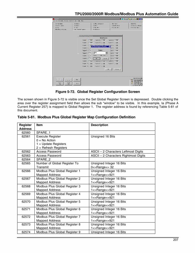
TPU2000/2000R Modbus/Modbus Plus Automation Guide
207
Figure 5-72. Global Register Configuration Screen
The screen shown in Figure 5-72 is visible once the Set Global Register Screen is depressed. Double clicking thearea over the register assignment field then allows the sub “window” to be visible. In this example, Ia (Phase ACurrent Register 257) is mapped to Global Register 1. The register address is found by referencing Table 5-81 ofthis document.
Table 5-81. Modbus Plus Global Register Map Configuration Definition
RegisterAddress
Item Description
62560 SPARE_162561 Execute Register
0 = No Action1 = Update Registers2 = Refresh Registers
Unsigned 16 Bits
62562 Access Password ASCII – 2 Characters Leftmost Digits62563 Access Password ASCII – 2 Characters Rightmost Digits62564 SPARE_262565 Number of Global Register To
TransmitUnsigned Integer 16 Bits0<=Range<= 32
62566 Modbus Plus Global Register 1Mapped Address
Unsigned Integer 16 Bits1<=Range<=921
62567 Modbus Plus Global Register 2Mapped Address
Unsigned Integer 16 Bits1<=Range<=921
62568 Modbus Plus Global Register 3Mapped Address
Unsigned Integer 16 Bits1<=Range<=921
62569 Modbus Plus Global Register 4Mapped Address
Unsigned Integer 16 Bits1<=Range<=921
62570 Modbus Plus Global Register 5Mapped Address
Unsigned Integer 16 Bits1<=Range<=921
62571 Modbus Plus Global Register 6Mapped Address
Unsigned Integer 16 Bits1<=Range<=921
62572 Modbus Plus Global Register 7Mapped Address
Unsigned Integer 16 Bits1<=Range<=921
62573 Modbus Plus Global Register 8Mapped Address
Unsigned Integer 16 Bits1<=Range<=921
62574 Modbus Plus Global Register 9 Unsigned Integer 16 Bits
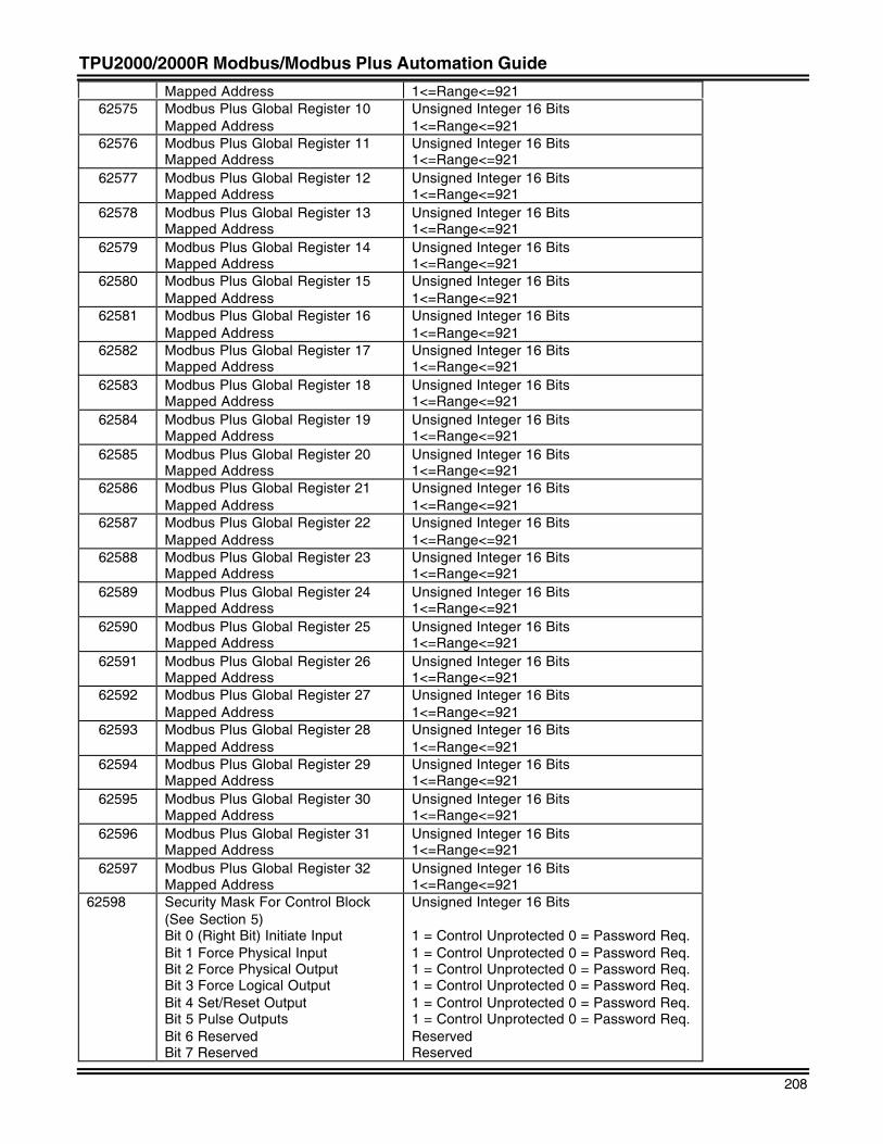
TPU2000/2000R Modbus/Modbus Plus Automation Guide
208
Mapped Address 1<=Range<=92162575 Modbus Plus Global Register 10
Mapped AddressUnsigned Integer 16 Bits1<=Range<=921
62576 Modbus Plus Global Register 11Mapped Address
Unsigned Integer 16 Bits1<=Range<=921
62577 Modbus Plus Global Register 12Mapped Address
Unsigned Integer 16 Bits1<=Range<=921
62578 Modbus Plus Global Register 13Mapped Address
Unsigned Integer 16 Bits1<=Range<=921
62579 Modbus Plus Global Register 14Mapped Address
Unsigned Integer 16 Bits1<=Range<=921
62580 Modbus Plus Global Register 15Mapped Address
Unsigned Integer 16 Bits1<=Range<=921
62581 Modbus Plus Global Register 16Mapped Address
Unsigned Integer 16 Bits1<=Range<=921
62582 Modbus Plus Global Register 17Mapped Address
Unsigned Integer 16 Bits1<=Range<=921
62583 Modbus Plus Global Register 18Mapped Address
Unsigned Integer 16 Bits1<=Range<=921
62584 Modbus Plus Global Register 19Mapped Address
Unsigned Integer 16 Bits1<=Range<=921
62585 Modbus Plus Global Register 20Mapped Address
Unsigned Integer 16 Bits1<=Range<=921
62586 Modbus Plus Global Register 21Mapped Address
Unsigned Integer 16 Bits1<=Range<=921
62587 Modbus Plus Global Register 22Mapped Address
Unsigned Integer 16 Bits1<=Range<=921
62588 Modbus Plus Global Register 23Mapped Address
Unsigned Integer 16 Bits1<=Range<=921
62589 Modbus Plus Global Register 24Mapped Address
Unsigned Integer 16 Bits1<=Range<=921
62590 Modbus Plus Global Register 25Mapped Address
Unsigned Integer 16 Bits1<=Range<=921
62591 Modbus Plus Global Register 26Mapped Address
Unsigned Integer 16 Bits1<=Range<=921
62592 Modbus Plus Global Register 27Mapped Address
Unsigned Integer 16 Bits1<=Range<=921
62593 Modbus Plus Global Register 28Mapped Address
Unsigned Integer 16 Bits1<=Range<=921
62594 Modbus Plus Global Register 29Mapped Address
Unsigned Integer 16 Bits1<=Range<=921
62595 Modbus Plus Global Register 30Mapped Address
Unsigned Integer 16 Bits1<=Range<=921
62596 Modbus Plus Global Register 31Mapped Address
Unsigned Integer 16 Bits1<=Range<=921
62597 Modbus Plus Global Register 32Mapped Address
Unsigned Integer 16 Bits1<=Range<=921
62598 Security Mask For Control Block(See Section 5)Bit 0 (Right Bit) Initiate InputBit 1 Force Physical InputBit 2 Force Physical OutputBit 3 Force Logical OutputBit 4 Set/Reset OutputBit 5 Pulse OutputsBit 6 ReservedBit 7 Reserved
Unsigned Integer 16 Bits
1 = Control Unprotected 0 = Password Req.1 = Control Unprotected 0 = Password Req.1 = Control Unprotected 0 = Password Req.1 = Control Unprotected 0 = Password Req.1 = Control Unprotected 0 = Password Req.1 = Control Unprotected 0 = Password Req.ReservedReserved
TPU2000/2000R Modbus/Modbus Plus Automation Guide
209
Bit 8 ReservedBit 9 ReservedBit 10 ReservedBit 11 ReservedBit 12 ReservedBit 13 ReservedBit 14 ReservedBit 15 Reserved
ReservedReservedReservedReservedReservedReservedReservedReserved
User Definable Register Configuration Block
As described in Section 5 the TPU2000 and TPU2000R has the capability to scale and remap the Modbusregisters within the unit. As shown in Table 5-82.
The following registers support modification and scaling of information contained in the Modbus user register set.The information in the 4xxxx registers can be tailored to the users needs with the following options:
1. Register: Register needed can be programmed.2. Scalability: Data in the registers can be scaled.3. Destination register data type: This supports multiple data types to match the destination systems needs.4. Destination register data size: This supports multiple data sizes to match the destination systems needs.5. MSB/LSB bit justification: This allows users to shift the bits contained in the 4xxxx register into the Most
significant bits or the Least significant bits.
Here is an example of how to set up the modbus registers to exploit the above facilities. Consider a situationwhere the destination system is a SCADA. Suppose the user’s SCADA system is setup to read the SystemFrequency on Register 40001 and requires the data be in the 12 Most significant bits. Also, let us suppose thatthe scale required on the system frequency is hex 0a (10 decimal) and the SCADA stores the value in a bipolardata type. The user would adopt the following procedure to setup register 40001 to meet the specifications of thedestination system. Now write hex 0a (decimal 10) which is the scale we need into Register 62693. Next writehex 0232 (562 decimal) on Register 62694 which fetches the value from the Register 40562 (the source registerfor system frequency). Setting the data size (12), the data type (bipolar) and shifting data (into Most significantbits) is done as follows:
Register Size (12 bits)
Bit 7 Bit 6 Bit 5 Bit 4
0 0 1 1
MSB/LSB (Justified to the left i.e. data in the the Most Significant Bits)
Bit 3
1
Register Type (Bipolar)
Bit 2 Bit 1 Bit 0
0 0 1
So, write hex 039 (decimal 57) into Register 62695 and the registers should look like:
register 62692 hex 0000rreeggiiss tteerr 6622669933 hheexx 000000aaregister 62694 hex 0232register 62695 hex 0039
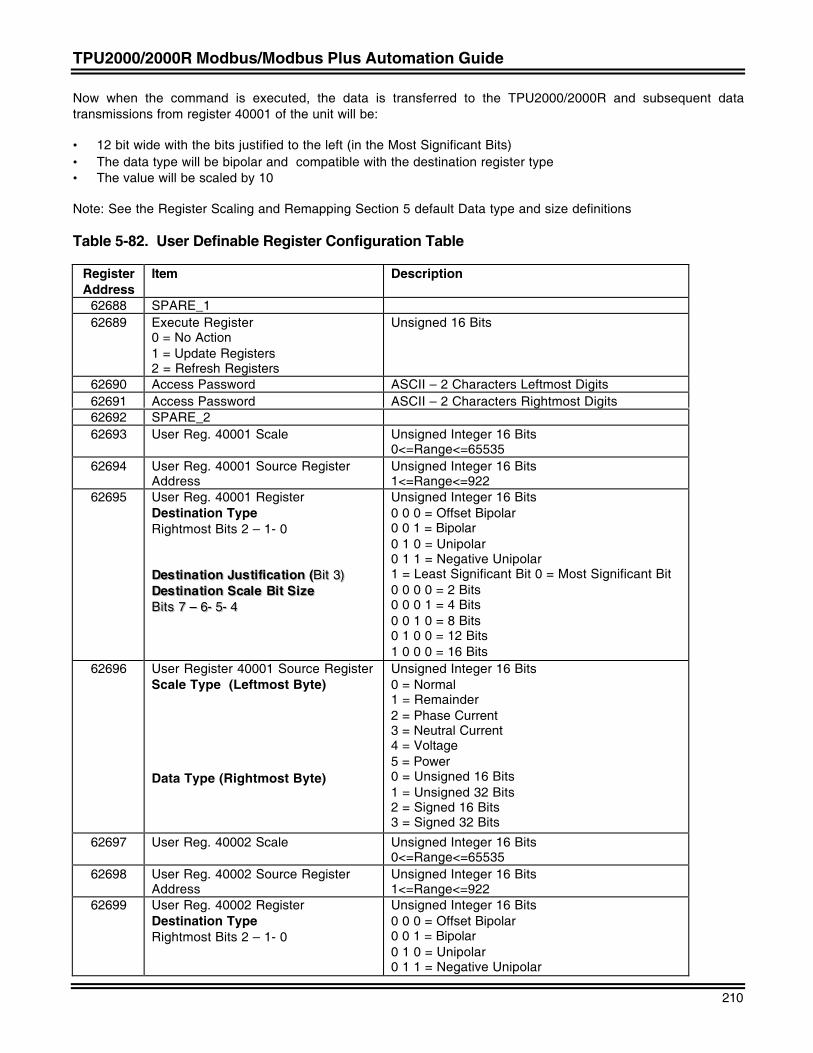
TPU2000/2000R Modbus/Modbus Plus Automation Guide
210
Now when the command is executed, the data is transferred to the TPU2000/2000R and subsequent datatransmissions from register 40001 of the unit will be:
• 12 bit wide with the bits justified to the left (in the Most Significant Bits)• The data type will be bipolar and compatible with the destination register type• The value will be scaled by 10
Note: See the Register Scaling and Remapping Section 5 default Data type and size definitions
Table 5-82. User Definable Register Configuration Table
RegisterAddress
Item Description
62688 SPARE_162689 Execute Register
0 = No Action1 = Update Registers2 = Refresh Registers
Unsigned 16 Bits
62690 Access Password ASCII – 2 Characters Leftmost Digits62691 Access Password ASCII – 2 Characters Rightmost Digits62692 SPARE_262693 User Reg. 40001 Scale Unsigned Integer 16 Bits
0<=Range<=6553562694 User Reg. 40001 Source Register
AddressUnsigned Integer 16 Bits1<=Range<=922
62695 User Reg. 40001 RegisterDestination TypeRightmost Bits 2 – 1- 0
DDeess ttiinnaa ttiioonn JJuuss ttii ffiiccaa ttiioonn ((BBiitt 33))DDeess ttiinnaa ttiioonn SSccaallee BBii tt SSiizzeeBBiittss 77 –– 66-- 55-- 44
Unsigned Integer 16 Bits0 0 0 = Offset Bipolar0 0 1 = Bipolar0 1 0 = Unipolar0 1 1 = Negative Unipolar1 = Least Significant Bit 0 = Most Significant Bit0 0 0 0 = 2 Bits0 0 0 1 = 4 Bits0 0 1 0 = 8 Bits0 1 0 0 = 12 Bits1 0 0 0 = 16 Bits
62696 User Register 40001 Source RegisterScale Type (Leftmost Byte)
Data Type (Rightmost Byte)
Unsigned Integer 16 Bits0 = Normal1 = Remainder2 = Phase Current3 = Neutral Current4 = Voltage5 = Power0 = Unsigned 16 Bits1 = Unsigned 32 Bits2 = Signed 16 Bits3 = Signed 32 Bits
62697 User Reg. 40002 Scale Unsigned Integer 16 Bits0<=Range<=65535
62698 User Reg. 40002 Source RegisterAddress
Unsigned Integer 16 Bits1<=Range<=922
62699 User Reg. 40002 RegisterDestination TypeRightmost Bits 2 – 1- 0
Unsigned Integer 16 Bits0 0 0 = Offset Bipolar0 0 1 = Bipolar0 1 0 = Unipolar0 1 1 = Negative Unipolar
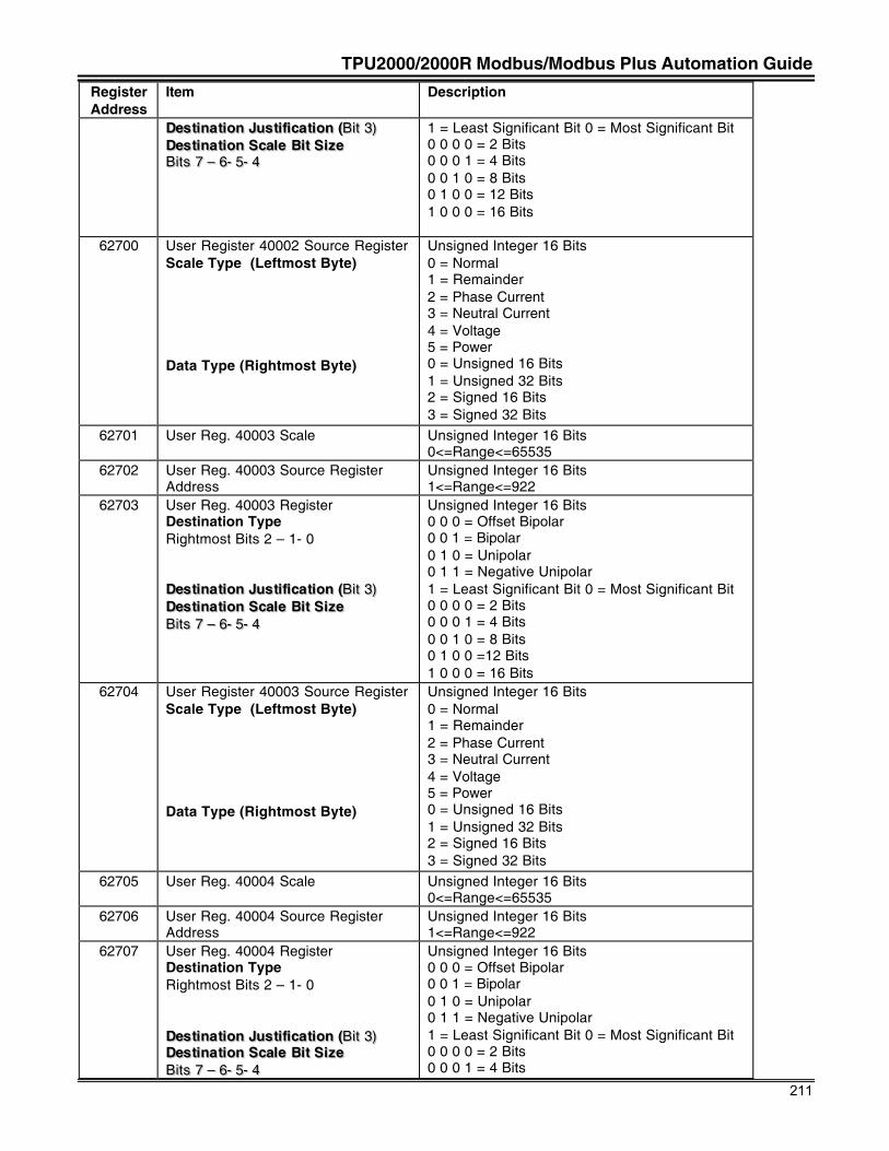
TPU2000/2000R Modbus/Modbus Plus Automation Guide
211
RegisterAddress
Item Description
DDeess ttiinnaa ttiioonn JJuuss ttii ffiiccaa ttiioonn ((BBiitt 33))DDeess ttiinnaa ttiioonn SSccaallee BBii tt SSiizzeeBBiittss 77 –– 66-- 55-- 44
1 = Least Significant Bit 0 = Most Significant Bit0 0 0 0 = 2 Bits0 0 0 1 = 4 Bits0 0 1 0 = 8 Bits0 1 0 0 = 12 Bits1 0 0 0 = 16 Bits
62700 User Register 40002 Source RegisterScale Type (Leftmost Byte)
Data Type (Rightmost Byte)
Unsigned Integer 16 Bits0 = Normal1 = Remainder2 = Phase Current3 = Neutral Current4 = Voltage5 = Power0 = Unsigned 16 Bits1 = Unsigned 32 Bits2 = Signed 16 Bits3 = Signed 32 Bits
62701 User Reg. 40003 Scale Unsigned Integer 16 Bits0<=Range<=65535
62702 User Reg. 40003 Source RegisterAddress
Unsigned Integer 16 Bits1<=Range<=922
62703 User Reg. 40003 RegisterDestination TypeRightmost Bits 2 – 1- 0
DDeess ttiinnaa ttiioonn JJuuss ttii ffiiccaa ttiioonn ((BBiitt 33))DDeess ttiinnaa ttiioonn SSccaallee BBii tt SSiizzeeBBiittss 77 –– 66-- 55-- 44
Unsigned Integer 16 Bits0 0 0 = Offset Bipolar0 0 1 = Bipolar0 1 0 = Unipolar0 1 1 = Negative Unipolar1 = Least Significant Bit 0 = Most Significant Bit0 0 0 0 = 2 Bits0 0 0 1 = 4 Bits0 0 1 0 = 8 Bits0 1 0 0 =12 Bits1 0 0 0 = 16 Bits
62704 User Register 40003 Source RegisterScale Type (Leftmost Byte)
Data Type (Rightmost Byte)
Unsigned Integer 16 Bits0 = Normal1 = Remainder2 = Phase Current3 = Neutral Current4 = Voltage5 = Power0 = Unsigned 16 Bits1 = Unsigned 32 Bits2 = Signed 16 Bits3 = Signed 32 Bits
62705 User Reg. 40004 Scale Unsigned Integer 16 Bits0<=Range<=65535
62706 User Reg. 40004 Source RegisterAddress
Unsigned Integer 16 Bits1<=Range<=922
62707 User Reg. 40004 RegisterDestination TypeRightmost Bits 2 – 1- 0
DDeess ttiinnaa ttiioonn JJuuss ttii ffiiccaa ttiioonn ((BBiitt 33))DDeess ttiinnaa ttiioonn SSccaallee BBii tt SSiizzeeBBiittss 77 –– 66-- 55-- 44
Unsigned Integer 16 Bits0 0 0 = Offset Bipolar0 0 1 = Bipolar0 1 0 = Unipolar0 1 1 = Negative Unipolar1 = Least Significant Bit 0 = Most Significant Bit0 0 0 0 = 2 Bits0 0 0 1 = 4 Bits
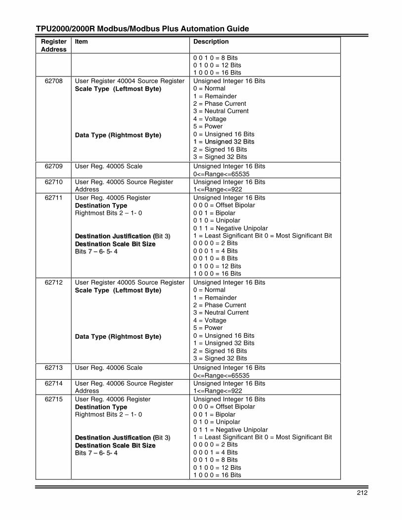
TPU2000/2000R Modbus/Modbus Plus Automation Guide
212
RegisterAddress
Item Description
0 0 1 0 = 8 Bits0 1 0 0 = 12 Bits1 0 0 0 = 16 Bits
62708 User Register 40004 Source RegisterScale Type (Leftmost Byte)
Data Type (Rightmost Byte)
Unsigned Integer 16 Bits0 = Normal1 = Remainder2 = Phase Current3 = Neutral Current4 = Voltage5 = Power0 = Unsigned 16 Bits11 == UUnnss iiggnneedd 3322 BBiittss2 = Signed 16 Bits3 = Signed 32 Bits
62709 User Reg. 40005 Scale Unsigned Integer 16 Bits0<=Range<=65535
62710 User Reg. 40005 Source RegisterAddress
Unsigned Integer 16 Bits1<=Range<=922
62711 User Reg. 40005 RegisterDestination TypeRightmost Bits 2 – 1- 0
DDeess ttiinnaa ttiioonn JJuuss ttii ffiiccaa ttiioonn ((BBiitt 33))DDeess ttiinnaa ttiioonn SSccaallee BBii tt SSiizzeeBBiittss 77 –– 66-- 55-- 44
Unsigned Integer 16 Bits0 0 0 = Offset Bipolar0 0 1 = Bipolar0 1 0 = Unipolar0 1 1 = Negative Unipolar1 = Least Significant Bit 0 = Most Significant Bit0 0 0 0 = 2 Bits0 0 0 1 = 4 Bits0 0 1 0 = 8 Bits0 1 0 0 = 12 Bits1 0 0 0 = 16 Bits
62712 User Register 40005 Source RegisterScale Type (Leftmost Byte)
Data Type (Rightmost Byte)
Unsigned Integer 16 Bits0 = Normal1 = Remainder2 = Phase Current3 = Neutral Current4 = Voltage5 = Power0 = Unsigned 16 Bits1 = Unsigned 32 Bits2 = Signed 16 Bits3 = Signed 32 Bits
62713 User Reg. 40006 Scale Unsigned Integer 16 Bits0<=Range<=65535
62714 User Reg. 40006 Source RegisterAddress
Unsigned Integer 16 Bits1<=Range<=922
62715 User Reg. 40006 RegisterDestination TypeRightmost Bits 2 – 1- 0
DDeess ttiinnaa ttiioonn JJuuss ttii ffiiccaa ttiioonn ((BBiitt 33))DDeess ttiinnaa ttiioonn SSccaallee BBii tt SSiizzeeBBiittss 77 –– 66-- 55-- 44
Unsigned Integer 16 Bits0 0 0 = Offset Bipolar0 0 1 = Bipolar0 1 0 = Unipolar0 1 1 = Negative Unipolar1 = Least Significant Bit 0 = Most Significant Bit0 0 0 0 = 2 Bits0 0 0 1 = 4 Bits0 0 1 0 = 8 Bits0 1 0 0 = 12 Bits1 0 0 0 = 16 Bits
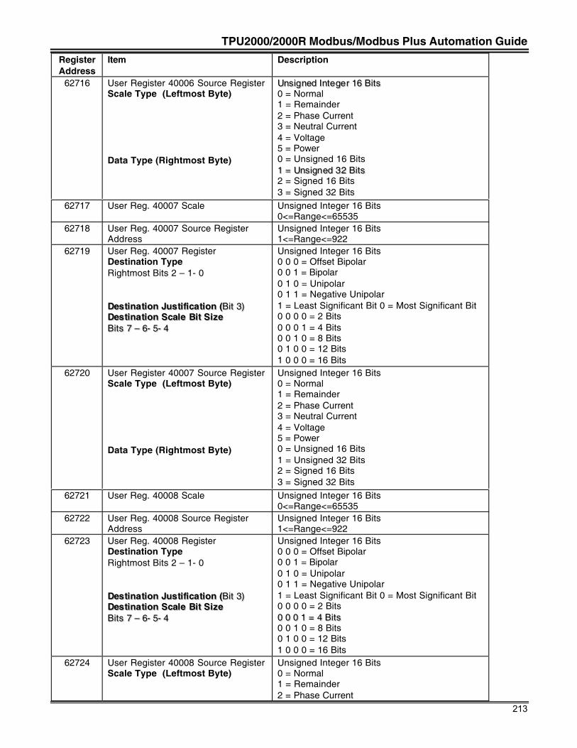
TPU2000/2000R Modbus/Modbus Plus Automation Guide
213
RegisterAddress
Item Description
62716 User Register 40006 Source RegisterScale Type (Leftmost Byte)
Data Type (Rightmost Byte)
UUnnss iiggnneedd IInntteeggee rr 1166 BBiittss0 = Normal1 = Remainder2 = Phase Current3 = Neutral Current4 = Voltage5 = Power0 = Unsigned 16 Bits11 == UUnnss iiggnneedd 3322 BBiittss2 = Signed 16 Bits3 = Signed 32 Bits
62717 User Reg. 40007 Scale Unsigned Integer 16 Bits0<=Range<=65535
62718 User Reg. 40007 Source RegisterAddress
Unsigned Integer 16 Bits1<=Range<=922
62719 User Reg. 40007 RegisterDestination TypeRightmost Bits 2 – 1- 0
DDeess ttiinnaa ttiioonn JJuuss ttii ffiiccaa ttiioonn ((BBiitt 33))DDeess ttiinnaa ttiioonn SSccaallee BBii tt SSiizzeeBBiittss 77 –– 66-- 55-- 44
Unsigned Integer 16 Bits0 0 0 = Offset Bipolar0 0 1 = Bipolar0 1 0 = Unipolar0 1 1 = Negative Unipolar1 = Least Significant Bit 0 = Most Significant Bit0 0 0 0 = 2 Bits0 0 0 1 = 4 Bits0 0 1 0 = 8 Bits0 1 0 0 = 12 Bits1 0 0 0 = 16 Bits
62720 User Register 40007 Source RegisterScale Type (Leftmost Byte)
Data Type (Rightmost Byte)
Unsigned Integer 16 Bits0 = Normal1 = Remainder2 = Phase Current3 = Neutral Current4 = Voltage5 = Power0 = Unsigned 16 Bits1 = Unsigned 32 Bits2 = Signed 16 Bits3 = Signed 32 Bits
62721 User Reg. 40008 Scale Unsigned Integer 16 Bits0<=Range<=65535
62722 User Reg. 40008 Source RegisterAddress
Unsigned Integer 16 Bits1<=Range<=922
62723 User Reg. 40008 RegisterDestination TypeRightmost Bits 2 – 1- 0
DDeess ttiinnaa ttiioonn JJuuss ttii ffiiccaa ttiioonn ((BBiitt 33))DDeess ttiinnaa ttiioonn SSccaallee BBii tt SSiizzeeBBiittss 77 –– 66-- 55-- 44
Unsigned Integer 16 Bits0 0 0 = Offset Bipolar0 0 1 = Bipolar0 1 0 = Unipolar0 1 1 = Negative Unipolar1 = Least Significant Bit 0 = Most Significant Bit0 0 0 0 = 2 Bits00 00 00 11 == 44 BBiittss0 0 1 0 = 8 Bits0 1 0 0 = 12 Bits1 0 0 0 = 16 Bits
62724 User Register 40008 Source RegisterScale Type (Leftmost Byte)
Unsigned Integer 16 Bits0 = Normal1 = Remainder2 = Phase Current
TPU2000/2000R Modbus/Modbus Plus Automation Guide
214
RegisterAddress
Item Description
Data Type (Rightmost Byte)
3 = Neutral Current4 = Voltage5 = Power0 = Unsigned 16 Bits1 = Unsigned 32 Bits2 = Signed 16 Bits3 = Signed 32 Bits
62725 User Reg. 40009 Scale Unsigned Integer 16 Bits0<=Range<=65535
62726 User Reg. 40009 Source RegisterAddress
Unsigned Integer 16 Bits1<=Range<=922
62727 User Reg. 40009 RegisterDestination TypeRightmost Bits 2 – 1- 0
DDeess ttiinnaa ttiioonn JJuuss ttii ffiiccaa ttiioonn ((BBiitt 33))DDeess ttiinnaa ttiioonn SSccaallee BBii tt SSiizzeeBBiittss 77 –– 66-- 55-- 44
Unsigned Integer 16 Bits0 0 0 = Offset Bipolar0 0 1 = Bipolar0 1 0 = Unipolar0 1 1 = Negative Unipolar1 = Least Significant Bit 0 = Most Significant Bit0 0 0 0 = 2 Bits0 0 0 1 = 4 Bits0 0 1 0 = 8 Bits0 1 0 0 = 12 Bits1 0 0 0 = 16 Bits
62728 User Register 40009 Source RegisterScale Type (Leftmost Byte)
Data Type (Rightmost Byte)
Unsigned Integer 16 Bits0 = Normal1 = Remainder2 = Phase Current3 = Neutral Current4 = Voltage5 = Power0 = Unsigned 16 Bits1 = Unsigned 32 Bits2 = Signed 16 Bits3 = Signed 32 Bits
62729 User Reg. 40010 Scale Unsigned Integer 16 Bits00<<==RRaannggee<<==6655553355
62730 User Reg. 40010 Source RegisterAddress
Unsigned Integer 16 Bits1<=Range<=922
62731 User Reg. 40010 RegisterDestination TypeRightmost Bits 2 – 1- 0
DDeess ttiinnaa ttiioonn JJuuss ttii ffiiccaa ttiioonn ((BBiitt 33))DDeess ttiinnaa ttiioonn SSccaallee BBii tt SSiizzeeBBiittss 77 –– 66-- 55-- 44
Unsigned Integer 16 Bits0 0 0 = Offset Bipolar0 0 1 = Bipolar0 1 0 = Unipolar0 1 1 = Negative Unipolar1 = Least Significant Bit 0 = Most Significant Bit0 0 0 0 = 2 Bits0 0 0 1 = 4 Bits0 0 1 0 = 8 Bits0 1 0 0 = 12 Bits1 0 0 0 = 16 Bits
62732 User Register 40010 Source RegisterScale Type (Leftmost Byte)
Unsigned Integer 16 Bits0 = Normal1 = Remainder2 = Phase Current3 = Neutral Current
TPU2000/2000R Modbus/Modbus Plus Automation Guide
215
RegisterAddress
Item Description
Data Type (Rightmost Byte)
4 = Voltage5 = Power0 = Unsigned 16 Bits1 = Unsigned 32 Bits2 = Signed 16 Bits3 = Signed 32 Bits
62733 User Reg. 40011 Scale Unsigned Integer 16 Bits0<=Range<=65535
62734 User Reg. 40011 Source RegisterAddress
Unsigned Integer 16 Bits1<=Range<=922
62735 User Reg. 40011 RegisterDestination TypeRightmost Bits 2 – 1- 0
DDeess ttiinnaa ttiioonn JJuuss ttii ffiiccaa ttiioonn ((BBiitt 33))DDeess ttiinnaa ttiioonn SSccaallee BBii tt SSiizzeeBBiittss 77 –– 66-- 55-- 44
Unsigned Integer 16 Bits0 0 0 = Offset Bipolar0 0 1 = Bipolar0 1 0 = Unipolar0 1 1 = Negative Unipolar1 = Least Significant Bit 0 = Most Significant Bit0 0 0 0 = 2 Bits0 0 0 1 = 4 Bits0 0 1 0 = 8 Bits0 1 0 0 = 12 Bits1 0 0 0 = 16 Bits
62736 User Register 40011 Source RegisterScale Type (Leftmost Byte)
Data Type (Rightmost Byte)
Unsigned Integer 16 Bits0 = Normal1 = Remainder2 = Phase Current3 = Neutral Current4 = Voltage5 = Power0 = Unsigned 16 Bits1 = Unsigned 32 Bits2 = Signed 16 Bits3 = Signed 32 Bits
62737 User Reg. 40012 Scale Unsigned Integer 16 Bits0<=Range<=65535
62738 User Reg. 40012 Source RegisterAddress
Unsigned Integer 16 Bits1<=Range<=922
62739 User Reg. 40012 RegisterDestination TypeRightmost Bits 2 – 1- 0
DDeess ttiinnaa ttiioonn JJuuss ttii ffiiccaa ttiioonn ((BBiitt 33))DDeess ttiinnaa ttiioonn SSccaallee BBii tt SSiizzeeBBiittss 77 –– 66-- 55-- 44
Unsigned Integer 16 Bits0 0 0 = Offset Bipolar0 0 1 = Bipolar0 1 0 = Unipolar0 1 1 = Negative Unipolar1 = Least Significant Bit 0 = Most Significant Bit0 0 0 0 = 2 Bits0 0 0 1 = 4 Bits0 0 1 0 = 8 Bits0 1 0 0 = 12 Bits1 0 0 0 = 16 Bits
62740 User Register 40012 Source RegisterScale Type (Leftmost Byte)
Data Type (Rightmost Byte)
Unsigned Integer 16 Bits0 = Normal1 = Remainder2 = Phase Current3 = Neutral Current4 = Voltage5 = Power0 = Unsigned 16 Bits1 = Unsigned 32 Bits
TPU2000/2000R Modbus/Modbus Plus Automation Guide
216
RegisterAddress
Item Description
2 = Signed 16 Bits3 = Signed 32 Bits
62741 User Reg. 40013 Scale Unsigned Integer 16 Bits0<=Range<=65535
62742 User Reg. 40013 Source RegisterAddress
Unsigned Integer 16 Bits1<=Range<=922
62743 User Reg. 40013 RegisterDestination TypeRightmost Bits 2 – 1- 0
DDeess ttiinnaa ttiioonn JJuuss ttii ffiiccaa ttiioonn ((BBiitt 33))DDeess ttiinnaa ttiioonn SSccaallee BBii tt SSiizzeeBBiittss 77 –– 66-- 55-- 44
Unsigned Integer 16 Bits0 0 0 = Offset Bipolar0 0 1 = Bipolar0 1 0 = Unipolar0 1 1 = Negative Unipolar1 = Least Significant Bit 0 = Most Significant Bit0 0 0 0 = 2 Bits0 0 0 1 = 4 Bits0 0 1 0 = 8 Bits0 1 0 0 = 12 Bits1 0 0 0 = 16 Bits
62744 User Register 40013 Source RegisterScale Type (Leftmost Byte)
Data Type (Rightmost Byte)
Unsigned Integer 16 Bits00 == NNoorrmm aall1 = Remainder2 = Phase Current3 = Neutral Current4 = Voltage5 = Power0 = Unsigned 16 Bits1 = Unsigned 32 Bits2 = Signed 16 Bits3 = Signed 32 Bits
62745 User Reg. 40014 Scale Unsigned Integer 16 Bits0<=Range<=65535
62746 User Reg. 40014 Source RegisterAddress
Unsigned Integer 16 Bits1<=Range<=922
62747 User Reg. 40014 RegisterDestination TypeRightmost Bits 2 – 1- 0
DDeess ttiinnaa ttiioonn JJuuss ttii ffiiccaa ttiioonn ((BBiitt 33))DDeess ttiinnaa ttiioonn SSccaallee BBii tt SSiizzeeBBiittss 77 –– 66-- 55-- 44
Unsigned Integer 16 Bits0 0 0 = Offset Bipolar0 0 1 = Bipolar0 1 0 = Unipolar0 1 1= Negative Unipolar1 = Least Significant Bit 0 = Most Significant Bit0 0 0 0 = 2 Bits0 0 0 1 = 4 Bits0 0 1 0 = 8 Bits0 1 0 0 = 12 Bits1 0 0 0 = 16 Bits
62748 User Register 40014 Source RegisterScale Type (Leftmost Byte)
Data Type (Rightmost Byte)
Unsigned Integer 16 Bits0 = Normal1 = Remainder2 = Phase Current3 = Neutral Current4 = Voltage5 = Power0 = Unsigned 16 Bits1 = Unsigned 32 Bits2 = Signed 16 Bits3 = Signed 32 Bits
62749 User Reg. 40015 Scale Unsigned Integer 16 Bits
TPU2000/2000R Modbus/Modbus Plus Automation Guide
217
RegisterAddress
Item Description
0<=Range<=6553562750 User Reg. 40015 Source Register
AddressUnsigned Integer 16 Bits1<=Range<=922
62751 User Reg. 40015 RegisterDestination TypeRightmost Bits 2 – 1- 0
DDeess ttiinnaa ttiioonn JJuuss ttii ffiiccaa ttiioonn ((BBiitt 33))DDeess ttiinnaa ttiioonn SSccaallee BBii tt SSiizzeeBBiittss 77 –– 66-- 55-- 44
Unsigned Integer 16 Bits0 0 0 = Offset Bipolar0 0 1 = Bipolar0 1 0 = Unipolar0 1 1 = Negative Unipolar1 = Least Significant Bit 0 = Most Significant Bit0 0 0 0 = 2 Bits0 0 0 1 = 4 Bits0 0 1 0 = 8 Bits0 1 0 0 = 12 Bits1 0 0 0 = 16 Bits
62752 User Register 40015 Source RegisterScale Type (Leftmost Byte)
Data Type (Rightmost Byte)
Unsigned Integer 16 Bits0 = Normal1 = Remainder2 = Phase Current3 = Neutral Current4 = Voltage55 == PPoowweerr0 = Unsigned 16 Bits1 = Unsigned 32 Bits2 = Signed 16 Bits3 = Signed 32 Bits
62753 User Reg. 40016 Scale Unsigned Integer 16 Bits0<=Range<=65535
62754 User Reg. 40016 Source RegisterAddress
Unsigned Integer 16 Bits1<=Range<=922
62755 User Reg. 40016 RegisterDestination TypeRightmost Bits 2 – 1- 0
DDeess ttiinnaa ttiioonn JJuuss ttii ffiiccaa ttiioonn ((BBiitt 33))DDeess ttiinnaa ttiioonn SSccaallee BBii tt SSiizzeeBBiittss 77 –– 66-- 55-- 44
Unsigned Integer 16 Bits0 0 0 = Offset Bipolar0 0 1 = Bipolar0 1 0 = Unipolar0 1 1 = Negative Unipolar1 = Least Significant Bit 0 = Most Significant Bit0 0 0 0 = 2 Bits0 0 0 1 =4 Bits00 00 11 00 == 88 BBiittss0 1 0 0 = 12 Bits1 0 0 0 = 16 Bits
62756 User Register 40016 Source RegisterScale Type (Leftmost Byte)
Data Type (Rightmost Byte)
Unsigned Integer 16 Bits0 = Normal1 = Remainder2 = Phase Current3 = Neutral Current4 = Voltage5 = Power0 = Unsigned 16 Bits1 = Unsigned 32 Bits2 = Signed 16 Bits3 = Signed 32 Bits
62757 User Reg. 40017 Scale Unsigned Integer 16 Bits0<=Range<=65535
62758 User Reg. 40017 Source RegisterAddress
Unsigned Integer 16 Bits1<=Range<=922
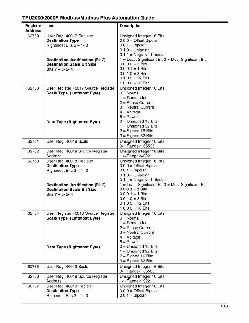
TPU2000/2000R Modbus/Modbus Plus Automation Guide
218
RegisterAddress
Item Description
62759 User Reg. 40017 RegisterDestination TypeRightmost Bits 2 – 1- 0
DDeess ttiinnaa ttiioonn JJuuss ttii ffiiccaa ttiioonn ((BBiitt 33))DDeess ttiinnaa ttiioonn SSccaallee BBii tt SSiizzeeBBiittss 77 –– 66-- 55-- 44
Unsigned Integer 16 Bits0 0 0 = Offset Bipolar0 0 1 = Bipolar0 1 0 = Unipolar0 1 1 = Negative Unipolar1 = Least Significant Bit 0 = Most Significant Bit0 0 0 0 = 2 Bits0 0 0 1 = 4 Bits0 0 1 0 = 8 Bits0 1 0 0 = 12 Bits1 0 0 0 = 16 Bits
62760 User Register 40017 Source RegisterScale Type (Leftmost Byte)
Data Type (Rightmost Byte)
Unsigned Integer 16 Bits0 = Normal1 = Remainder2 = Phase Current3 = Neutral Current4 = Voltage5 = Power0 = Unsigned 16 Bits1 = Unsigned 32 Bits2 = Signed 16 Bits3 = Signed 32 Bits
62761 User Reg. 40018 Scale Unsigned Integer 16 Bits0<=Range<=65535
62762 User Reg. 40018 Source RegisterAddress
UUnnss iiggnneedd IInntteeggee rr 1166 BBiittss1<=Range<=922
62763 User Reg. 40018 RegisterDestination TypeRightmost Bits 2 – 1- 0
DDeess ttiinnaa ttiioonn JJuuss ttii ffiiccaa ttiioonn ((BBiitt 33))DDeess ttiinnaa ttiioonn SSccaallee BBii tt SSiizzeeBBiittss 77 –– 66-- 55-- 44
Unsigned Integer 16 Bits0 0 0 = Offset Bipolar0 0 1 = Bipolar0 1 0 = Unipolar0 1 1 = Negative Unipolar1 = Least Significant Bit 0 = Most Significant Bit00 00 00 00 == 22 BBiittss0 0 0 1 = 4 Bits0 0 1 0 = 8 Bits0 1 0 0 = 12 Bits1 0 0 0 = 16 Bits
62764 User Register 40018 Source RegisterScale Type (Leftmost Byte)
Data Type (Rightmost Byte)
Unsigned Integer 16 Bits0 = Normal1 = Remainder2 = Phase Current3 = Neutral Current4 = Voltage5 = Power0 = Unsigned 16 Bits1 = Unsigned 32 Bits2 = Signed 16 Bits3 = Signed 32 Bits
62765 User Reg. 40019 Scale Unsigned Integer 16 Bits0<=Range<=65535
62766 User Reg. 40019 Source RegisterAddress
Unsigned Integer 16 Bits1<=Range<=922
62767 User Reg. 40019 RegisterDestination TypeRightmost Bits 2 – 1- 0
Unsigned Integer 16 Bits0 0 0 = Offset Bipolar0 0 1 = Bipolar
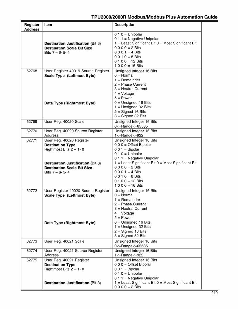
TPU2000/2000R Modbus/Modbus Plus Automation Guide
219
RegisterAddress
Item Description
DDeess ttiinnaa ttiioonn JJuuss ttii ffiiccaa ttiioonn ((BBiitt 33))DDeess ttiinnaa ttiioonn SSccaallee BBii tt SSiizzeeBBiittss 77 –– 66-- 55-- 44
0 1 0 = Unipolar0 1 1 = Negative Unipolar1 = Least Significant Bit 0 = Most Significant Bit0 0 0 0 = 2 Bits0 0 0 1 = 4 Bits0 0 1 0 = 8 Bits0 1 0 0 = 12 Bits1 0 0 0 = 16 Bits
62768 User Register 40019 Source RegisterScale Type (Leftmost Byte)
Data Type (Rightmost Byte)
UUnnss iiggnneedd IInntteeggee rr 1166 BBiittss0 = Normal1 = Remainder2 = Phase Current3 = Neutral Current4 = Voltage5 = Power0 = Unsigned 16 Bits1 = Unsigned 32 Bits22 == SSiiggnneedd 1166 BBiittss3 = Signed 32 Bits
62769 User Reg. 40020 Scale Unsigned Integer 16 Bits0<=Range<=65535
62770 User Reg. 40020 Source RegisterAddress
Unsigned Integer 16 Bits1<=Range<=922
62771 User Reg. 40020 RegisterDestination TypeRightmost Bits 2 – 1- 0
DDeess ttiinnaa ttiioonn JJuuss ttii ffiiccaa ttiioonn ((BBiitt 33))DDeess ttiinnaa ttiioonn SSccaallee BBii tt SSiizzeeBBiittss 77 –– 66-- 55-- 44
Unsigned Integer 16 Bits0 0 0 = Offset Bipolar0 0 1 = Bipolar0 1 0 = Unipolar0 1 1 = Negative Unipolar1 = Least Significant Bit 0 = Most Significant Bit0 0 0 0 = 2 Bits0 0 0 1 = 4 Bits0 0 1 0 = 8 Bits0 1 0 0 = 12 Bits1 0 0 0 = 16 Bits
62772 User Register 40020 Source RegisterScale Type (Leftmost Byte)
Data Type (Rightmost Byte)
Unsigned Integer 16 Bits0 = Normal1 = Remainder2 = Phase Current3 = Neutral Current4 = Voltage5 = Power0 = Unsigned 16 Bits1 = Unsigned 32 Bits2 = Signed 16 Bits3 = Signed 32 Bits
62773 User Reg. 40021 Scale Unsigned Integer 16 Bits0<=Range<=65535
62774 User Reg. 40021 Source RegisterAddress
UUnnss iiggnneedd IInntteeggee rr 1166 BBiittss1<=Range<=922
62775 User Reg. 40021 RegisterDestination TypeRightmost Bits 2 – 1- 0
DDeess ttiinnaa ttiioonn JJuuss ttii ffiiccaa ttiioonn ((BBiitt 33))
Unsigned Integer 16 Bits0 0 0 = Offset Bipolar0 0 1 = Bipolar0 1 0 = Unipolar0 1 1 = Negative Unipolar1 = Least Significant Bit 0 = Most Significant Bit0 0 0 0 = 2 Bits
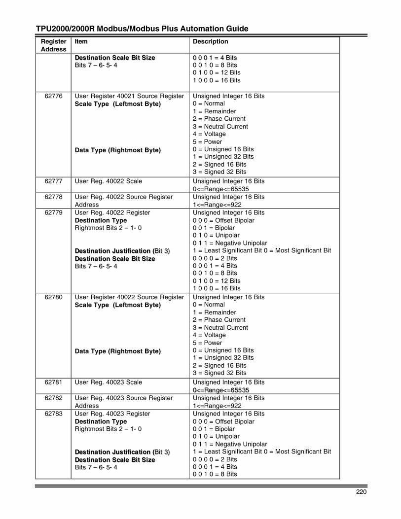
TPU2000/2000R Modbus/Modbus Plus Automation Guide
220
RegisterAddress
Item Description
DDeess ttiinnaa ttiioonn SSccaallee BBii tt SSiizzeeBBiittss 77 –– 66-- 55-- 44
00 00 00 11 == 44 BBiittss0 0 1 0 = 8 Bits0 1 0 0 = 12 Bits1 0 0 0 = 16 Bits
62776 User Register 40021 Source RegisterScale Type (Leftmost Byte)
Data Type (Rightmost Byte)
Unsigned Integer 16 Bits0 = Normal1 = Remainder2 = Phase Current3 = Neutral Current4 = Voltage5 = Power0 = Unsigned 16 Bits1 = Unsigned 32 Bits2 = Signed 16 Bits3 = Signed 32 Bits
62777 User Reg. 40022 Scale Unsigned Integer 16 Bits0<=Range<=65535
62778 User Reg. 40022 Source RegisterAddress
Unsigned Integer 16 Bits1<=Range<=922
62779 User Reg. 40022 RegisterDestination TypeRightmost Bits 2 – 1- 0
DDeess ttiinnaa ttiioonn JJuuss ttii ffiiccaa ttiioonn ((BBiitt 33))DDeess ttiinnaa ttiioonn SSccaallee BBii tt SSiizzeeBBiittss 77 –– 66-- 55-- 44
Unsigned Integer 16 Bits0 0 0 = Offset Bipolar0 0 1 = Bipolar0 1 0 = Unipolar0 1 1 = Negative Unipolar1 = Least Significant Bit 0 = Most Significant Bit0 0 0 0 = 2 Bits0 0 0 1 = 4 Bits0 0 1 0 = 8 Bits0 1 0 0 = 12 Bits1 0 0 0 = 16 Bits
62780 User Register 40022 Source RegisterScale Type (Leftmost Byte)
Data Type (Rightmost Byte)
Unsigned Integer 16 Bits0 = Normal1 = Remainder2 = Phase Current3 = Neutral Current4 = Voltage5 = Power0 = Unsigned 16 Bits1 = Unsigned 32 Bits2 = Signed 16 Bits3 = Signed 32 Bits
62781 User Reg. 40023 Scale Unsigned Integer 16 Bits00<<==RRaannggee<<==6655553355
62782 User Reg. 40023 Source RegisterAddress
Unsigned Integer 16 Bits1<=Range<=922
62783 User Reg. 40023 RegisterDestination TypeRightmost Bits 2 – 1- 0
DDeess ttiinnaa ttiioonn JJuuss ttii ffiiccaa ttiioonn ((BBiitt 33))DDeess ttiinnaa ttiioonn SSccaallee BBii tt SSiizzeeBBiittss 77 –– 66-- 55-- 44
Unsigned Integer 16 Bits0 0 0 = Offset Bipolar0 0 1 = Bipolar0 1 0 = Unipolar0 1 1 = Negative Unipolar1 = Least Significant Bit 0 = Most Significant Bit0 0 0 0 = 2 Bits0 0 0 1 = 4 Bits0 0 1 0 = 8 Bits
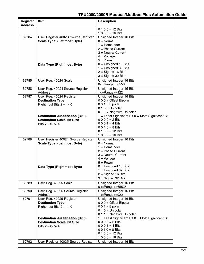
TPU2000/2000R Modbus/Modbus Plus Automation Guide
221
RegisterAddress
Item Description
0 1 0 0 = 12 Bits1 0 0 0 = 16 Bits
62784 User Register 40023 Source RegisterScale Type (Leftmost Byte)
Data Type (Rightmost Byte)
Unsigned Integer 16 Bits0 = Normal1 = Remainder2 = Phase Current33 == NNeeuutt rraall CCuu rrrreenntt4 = Voltage5 = Power0 = Unsigned 16 Bits1 = Unsigned 32 Bits2 = Signed 16 Bits3 = Signed 32 Bits
62785 User Reg. 40024 Scale Unsigned Integer 16 Bits0<=Range<=65535
62786 User Reg. 40024 Source RegisterAddress
Unsigned Integer 16 Bits1<=Range<=922
62787 User Reg. 40024 RegisterDestination TypeRightmost Bits 2 – 1- 0
DDeess ttiinnaa ttiioonn JJuuss ttii ffiiccaa ttiioonn ((BBiitt 33))DDeess ttiinnaa ttiioonn SSccaallee BBii tt SSiizzeeBBiittss 77 –– 66-- 55-- 44
Unsigned Integer 16 Bits0 0 0 = Offset Bipolar0 0 1 = Bipolar0 1 0 = Unipolar0 1 1 = Negative Unipolar1 = Least Significant Bit 0 = Most Significant Bit0 0 0 0 = 2 Bits0 0 0 1 = 4 Bits0 0 1 0 = 8 Bits0 1 0 0 = 12 Bits1 0 0 0 = 16 Bits
62788 User Register 40024 Source RegisterScale Type (Leftmost Byte)
Data Type (Rightmost Byte)
Unsigned Integer 16 Bits0 = Normal1 = Remainder2 = Phase Current3 = Neutral Current4 = Voltage55 == PPoowweerr0 = Unsigned 16 Bits1 = Unsigned 32 Bits2 = Signed 16 Bits3 = Signed 32 Bits
62789 User Reg. 40025 Scale Unsigned Integer 16 Bits0<=Range<=65535
62790 User Reg. 40025 Source RegisterAddress
Unsigned Integer 16 Bits1<=Range<=922
62791 User Reg. 40025 RegisterDestination TypeRightmost Bits 2 – 1- 0
DDeess ttiinnaa ttiioonn JJuuss ttii ffiiccaa ttiioonn ((BBiitt 33))DDeess ttiinnaa ttiioonn SSccaallee BBii tt SSiizzeeBBiittss 77 –– 66-- 55-- 44
Unsigned Integer 16 Bits0 0 0 = Offset Bipolar0 0 1 = Bipolar0 1 0 = Unipolar0 1 1 = Negative Unipolar1 = Least Significant Bit 0 = Most Significant Bit0 0 0 0 = 2 Bits0 0 0 1 = 4 Bits00 00 11 00 == 88 BBiittss0 1 0 0 = 12 Bits1 0 0 0 = 16 Bits
62792 User Register 40025 Source Register Unsigned Integer 16 Bits
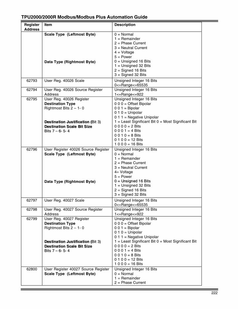
TPU2000/2000R Modbus/Modbus Plus Automation Guide
222
RegisterAddress
Item Description
Scale Type (Leftmost Byte)
Data Type (Rightmost Byte)
0 = Normal1 = Remainder2 = Phase Current3 = Neutral Current4 = Voltage5 = Power0 = Unsigned 16 Bits1 = Unsigned 32 Bits2 = Signed 16 Bits3 = Signed 32 Bits
62793 User Reg. 40026 Scale Unsigned Integer 16 Bits0<=Range<=65535
62794 User Reg. 40026 Source RegisterAddress
Unsigned Integer 16 Bits1<=Range<=922
62795 User Reg. 40026 RegisterDestination TypeRightmost Bits 2 – 1- 0
DDeess ttiinnaa ttiioonn JJuuss ttii ffiiccaa ttiioonn ((BBiitt 33))DDeess ttiinnaa ttiioonn SSccaallee BBii tt SSiizzeeBBiittss 77 –– 66-- 55-- 44
Unsigned Integer 16 Bits0 0 0 = Offset Bipolar0 0 1 = Bipolar0 1 0 = Unipolar0 1 1 = Negative Unipolar1 = Least Significant Bit 0 = Most Significant Bit0 0 0 0 = 2 Bits0 0 0 1 = 4 Bits0 0 1 0 = 8 Bits0 1 0 0 = 12 Bits1 0 0 0 = 16 Bits
62796 User Register 40026 Source RegisterScale Type (Leftmost Byte)
Data Type (Rightmost Byte)
Unsigned Integer 16 Bits0 = Normal1 = Remainder2 = Phase Current3 = Neutral Current4= Voltage5 = Power00 == UUnnss iiggnneedd 1166 BBiittss1 = Unsigned 32 Bits2 = Signed 16 Bits3 = Signed 32 Bits
62797 User Reg. 40027 Scale Unsigned Integer 16 Bits0<=Range<=65535
62798 User Reg. 40027 Source RegisterAddress
Unsigned Integer 16 Bits1<=Range<=922
62799 User Reg. 40027 RegisterDestination TypeRightmost Bits 2 – 1- 0
DDeess ttiinnaa ttiioonn JJuuss ttii ffiiccaa ttiioonn ((BBiitt 33))DDeess ttiinnaa ttiioonn SSccaallee BBii tt SSiizzeeBBiittss 77 –– 66-- 55-- 44
Unsigned Integer 16 Bits0 0 0 = Offset Bipolar0 0 1 = Bipolar0 1 0 = Unipolar0 1 1 = Negative Unipolar1 = Least Significant Bit 0 = Most Significant Bit0 0 0 0 = 2 Bits0 0 0 1 = 4 Bits0 0 1 0 = 8 Bits0 1 0 0 = 12 Bits1 0 0 0 = 16 Bits
62800 User Register 40027 Source RegisterScale Type (Leftmost Byte)
Unsigned Integer 16 Bits0 = Normal1 = Remainder2 = Phase Current
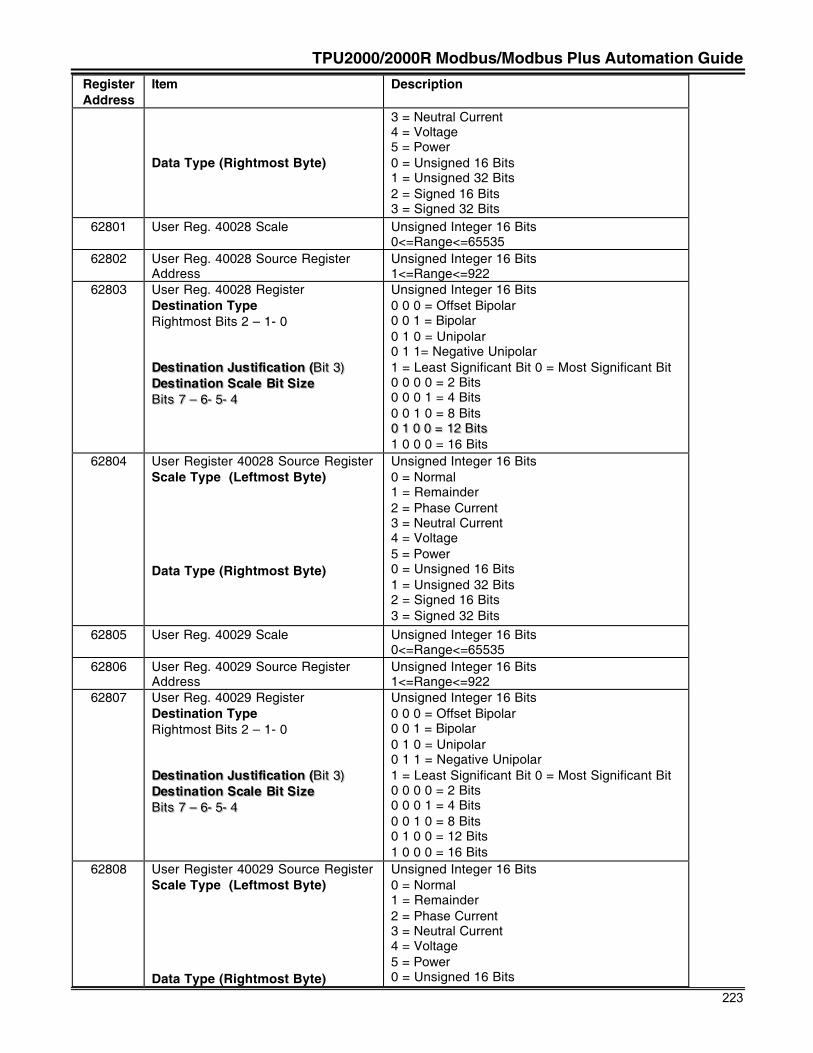
TPU2000/2000R Modbus/Modbus Plus Automation Guide
223
RegisterAddress
Item Description
Data Type (Rightmost Byte)
3 = Neutral Current4 = Voltage5 = Power0 = Unsigned 16 Bits1 = Unsigned 32 Bits2 = Signed 16 Bits3 = Signed 32 Bits
62801 User Reg. 40028 Scale Unsigned Integer 16 Bits0<=Range<=65535
62802 User Reg. 40028 Source RegisterAddress
Unsigned Integer 16 Bits1<=Range<=922
62803 User Reg. 40028 RegisterDestination TypeRightmost Bits 2 – 1- 0
DDeess ttiinnaa ttiioonn JJuuss ttii ffiiccaa ttiioonn ((BBiitt 33))DDeess ttiinnaa ttiioonn SSccaallee BBii tt SSiizzeeBBiittss 77 –– 66-- 55-- 44
Unsigned Integer 16 Bits0 0 0 = Offset Bipolar0 0 1 = Bipolar0 1 0 = Unipolar0 1 1= Negative Unipolar1 = Least Significant Bit 0 = Most Significant Bit0 0 0 0 = 2 Bits0 0 0 1 = 4 Bits0 0 1 0 = 8 Bits00 11 00 00 == 1122 BBiittss1 0 0 0 = 16 Bits
62804 User Register 40028 Source RegisterScale Type (Leftmost Byte)
Data Type (Rightmost Byte)
Unsigned Integer 16 Bits0 = Normal1 = Remainder2 = Phase Current3 = Neutral Current4 = Voltage5 = Power0 = Unsigned 16 Bits1 = Unsigned 32 Bits2 = Signed 16 Bits3 = Signed 32 Bits
62805 User Reg. 40029 Scale Unsigned Integer 16 Bits0<=Range<=65535
62806 User Reg. 40029 Source RegisterAddress
Unsigned Integer 16 Bits1<=Range<=922
62807 User Reg. 40029 RegisterDestination TypeRightmost Bits 2 – 1- 0
DDeess ttiinnaa ttiioonn JJuuss ttii ffiiccaa ttiioonn ((BBiitt 33))DDeess ttiinnaa ttiioonn SSccaallee BBii tt SSiizzeeBBiittss 77 –– 66-- 55-- 44
Unsigned Integer 16 Bits0 0 0 = Offset Bipolar0 0 1 = Bipolar0 1 0 = Unipolar0 1 1 = Negative Unipolar1 = Least Significant Bit 0 = Most Significant Bit0 0 0 0 = 2 Bits0 0 0 1 = 4 Bits0 0 1 0 = 8 Bits0 1 0 0 = 12 Bits1 0 0 0 = 16 Bits
62808 User Register 40029 Source RegisterScale Type (Leftmost Byte)
Data Type (Rightmost Byte)
Unsigned Integer 16 Bits0 = Normal1 = Remainder2 = Phase Current3 = Neutral Current4 = Voltage5 = Power0 = Unsigned 16 Bits
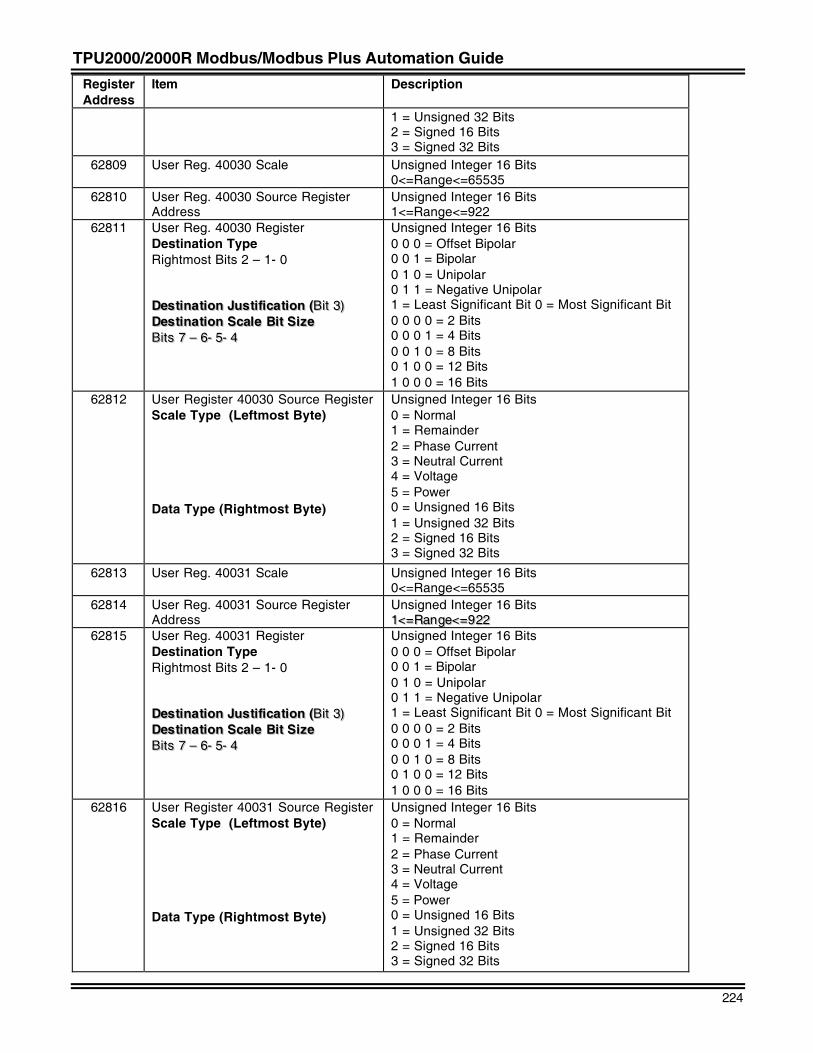
TPU2000/2000R Modbus/Modbus Plus Automation Guide
224
RegisterAddress
Item Description
1 = Unsigned 32 Bits2 = Signed 16 Bits3 = Signed 32 Bits
62809 User Reg. 40030 Scale Unsigned Integer 16 Bits0<=Range<=65535
62810 User Reg. 40030 Source RegisterAddress
Unsigned Integer 16 Bits1<=Range<=922
62811 User Reg. 40030 RegisterDestination TypeRightmost Bits 2 – 1- 0
DDeess ttiinnaa ttiioonn JJuuss ttii ffiiccaa ttiioonn ((BBiitt 33))DDeess ttiinnaa ttiioonn SSccaallee BBii tt SSiizzeeBBiittss 77 –– 66-- 55-- 44
Unsigned Integer 16 Bits0 0 0 = Offset Bipolar0 0 1 = Bipolar0 1 0 = Unipolar0 1 1 = Negative Unipolar1 = Least Significant Bit 0 = Most Significant Bit0 0 0 0 = 2 Bits0 0 0 1 = 4 Bits0 0 1 0 = 8 Bits0 1 0 0 = 12 Bits1 0 0 0 = 16 Bits
62812 User Register 40030 Source RegisterScale Type (Leftmost Byte)
Data Type (Rightmost Byte)
Unsigned Integer 16 Bits0 = Normal1 = Remainder2 = Phase Current3 = Neutral Current4 = Voltage5 = Power0 = Unsigned 16 Bits1 = Unsigned 32 Bits2 = Signed 16 Bits3 = Signed 32 Bits
62813 User Reg. 40031 Scale Unsigned Integer 16 Bits0<=Range<=65535
62814 User Reg. 40031 Source RegisterAddress
Unsigned Integer 16 Bits11<<==RRaannggee<<==992222
62815 User Reg. 40031 RegisterDestination TypeRightmost Bits 2 – 1- 0
DDeess ttiinnaa ttiioonn JJuuss ttii ffiiccaa ttiioonn ((BBiitt 33))DDeess ttiinnaa ttiioonn SSccaallee BBii tt SSiizzeeBBiittss 77 –– 66-- 55-- 44
Unsigned Integer 16 Bits0 0 0 = Offset Bipolar0 0 1 = Bipolar0 1 0 = Unipolar0 1 1 = Negative Unipolar1 = Least Significant Bit 0 = Most Significant Bit0 0 0 0 = 2 Bits0 0 0 1 = 4 Bits0 0 1 0 = 8 Bits0 1 0 0 = 12 Bits1 0 0 0 = 16 Bits
62816 User Register 40031 Source RegisterScale Type (Leftmost Byte)
Data Type (Rightmost Byte)
Unsigned Integer 16 Bits0 = Normal1 = Remainder2 = Phase Current3 = Neutral Current4 = Voltage5 = Power0 = Unsigned 16 Bits1 = Unsigned 32 Bits2 = Signed 16 Bits3 = Signed 32 Bits
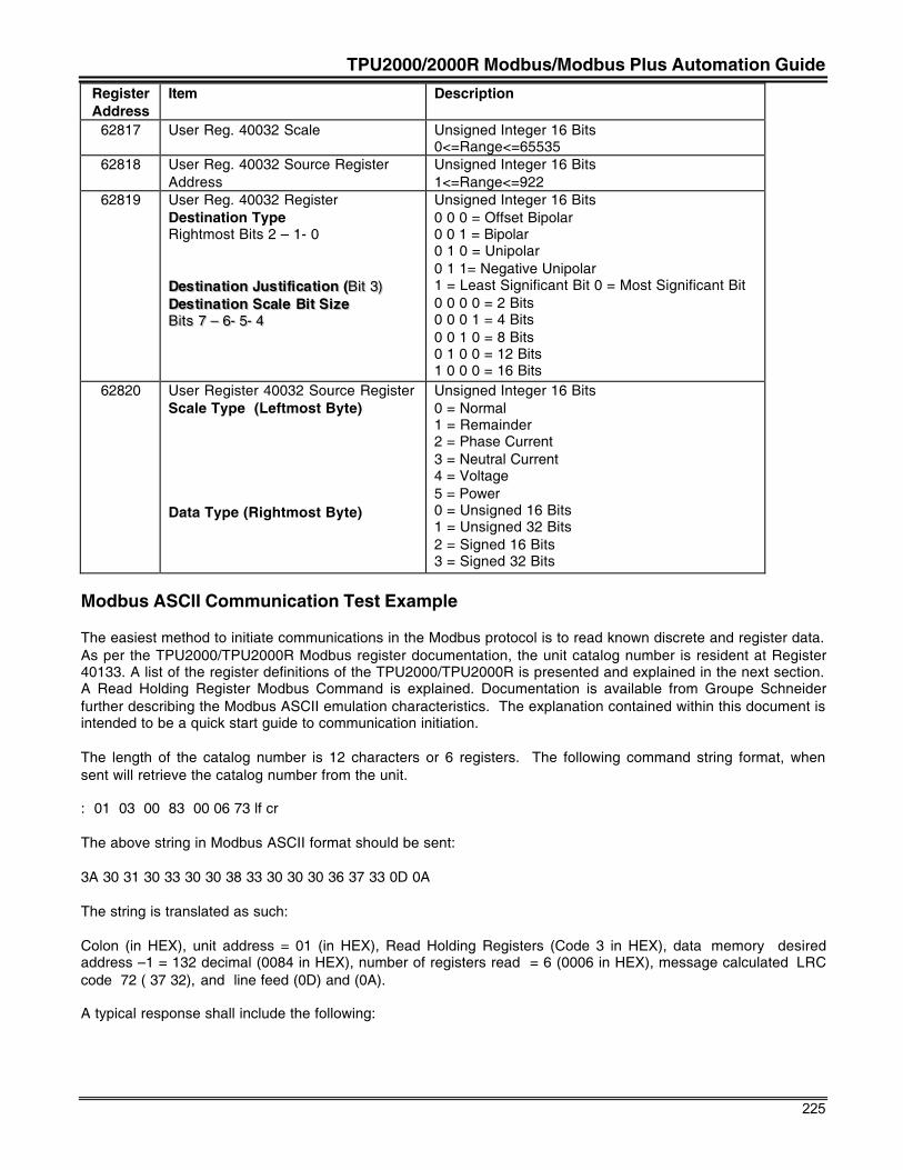
TPU2000/2000R Modbus/Modbus Plus Automation Guide
225
RegisterAddress
Item Description
62817 User Reg. 40032 Scale Unsigned Integer 16 Bits0<=Range<=65535
62818 User Reg. 40032 Source RegisterAddress
Unsigned Integer 16 Bits1<=Range<=922
62819 User Reg. 40032 RegisterDestination TypeRightmost Bits 2 – 1- 0
DDeess ttiinnaa ttiioonn JJuuss ttii ffiiccaa ttiioonn ((BBiitt 33))DDeess ttiinnaa ttiioonn SSccaallee BBii tt SSiizzeeBBiittss 77 –– 66-- 55-- 44
Unsigned Integer 16 Bits0 0 0 = Offset Bipolar0 0 1 = Bipolar0 1 0 = Unipolar0 1 1= Negative Unipolar1 = Least Significant Bit 0 = Most Significant Bit0 0 0 0 = 2 Bits0 0 0 1 = 4 Bits0 0 1 0 = 8 Bits0 1 0 0 = 12 Bits1 0 0 0 = 16 Bits
62820 User Register 40032 Source RegisterScale Type (Leftmost Byte)
Data Type (Rightmost Byte)
Unsigned Integer 16 Bits0 = Normal1 = Remainder2 = Phase Current3 = Neutral Current4 = Voltage5 = Power0 = Unsigned 16 Bits1 = Unsigned 32 Bits2 = Signed 16 Bits3 = Signed 32 Bits
Modbus ASCII Communication Test Example
The easiest method to initiate communications in the Modbus protocol is to read known discrete and register data.As per the TPU2000/TPU2000R Modbus register documentation, the unit catalog number is resident at Register40133. A list of the register definitions of the TPU2000/TPU2000R is presented and explained in the next section.A Read Holding Register Modbus Command is explained. Documentation is available from Groupe Schneiderfurther describing the Modbus ASCII emulation characteristics. The explanation contained within this document isintended to be a quick start guide to communication initiation.
The length of the catalog number is 12 characters or 6 registers. The following command string format, whensent will retrieve the catalog number from the unit.
: 01 03 00 83 00 06 73 lf cr
The above string in Modbus ASCII format should be sent:
3A 30 31 30 33 30 30 38 33 30 30 30 36 37 33 0D 0A
The string is translated as such:
Colon (in HEX), unit address = 01 (in HEX), Read Holding Registers (Code 3 in HEX), data memory desiredaddress –1 = 132 decimal (0084 in HEX), number of registers read = 6 (0006 in HEX), message calculated LRCcode 72 ( 37 32), and line feed (0D) and (0A).
A typical response shall include the following:
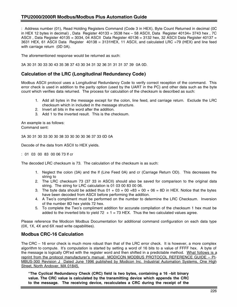
TPU2000/2000R Modbus/Modbus Plus Automation Guide
226
: Address number (01), Read Holding Registers Command (Code 3 in HEX), Byte Count Returned in decimal (0Cin HEX 12 bytes in decimal) , Data Register 40133 = 3538 hex – 58 ASCII, Data Register 40134= 3743 hex , 7CASCII , Data Register 40135 = 3034, 04 ASCII Data Register 40136 = 3132 hex, 32 ASCII Data Register 40137 =3631 HEX, 61 ASCII Data Register 40138 = 3131HEX, 11 ASCII, and calculated LRC =79 (HEX) and line feedwith carriage return (0D 0A).
The aforementioned response would be returned as such:
3A 30 31 30 33 30 43 35 38 37 43 30 34 31 32 36 31 31 31 37 39 0A 0D.
Calculation of the LRC (Longitudinal Redundancy Code)
Modbus ASCII protocol uses a Longitudinal Redundancy Code to verify correct reception of the command. Thiserror check is used in addition to the parity option (used by the UART in the PC) and other data such as the bytecount which verifies data returned. The process for calculation of the checksum is described as such:
1. Add all bytes in the message except for the colon, line feed, and carriage return. Exclude the LRCchecksum which in included in the message structure.
2. Invert all bits in the word after the addition.3. Add 1 to the inverted result. This is the checksum.
An example is as follows:Command sent:
3A 30 31 30 33 30 30 38 33 30 30 30 36 37 33 0D 0A
Decode of the data from ASCII to HEX yields.
: 01 03 00 83 00 06 73 lf cr
The decoded LRC checksum is 73. The calculation of the checksum is as such:
1. Neglect the colon (3A) and the lf (Line Feed 0A) and cr (Carriage Return OD). This decreases thestring to
2. The LRC checksum 73 (37 33 in ASCII) should also be saved for comparison to the original datastring. The string for LRC calculation is 01 03 00 83 00 06.
3. The byte data should be added thus 01 + 03 + 00 +83 + 00 + 06 = 8D in HEX. Notice that the byteshave been decoded from ASCII before performing the addition.
4. A Two’s compliment must be performed on the number to determine the LRC Checksum. Inversionof the number 8D hex yields 72 hex.
5. To complete the Two’s compliment addition for accurate compilation of the checksum 1 hex must beadded to the inverted bits to yield 72 + 1 = 73 HEX. Thus the two calculated values agree.
Please reference the Modicon Modbus Documentation for additional command configuration on each data type(0X, 1X, 4X and 6X read write capabilities).
Modbus CRC-16 Calculation
The CRC – 16 error check is much more robust than that of the LRC error check. It is however, a more complexalgorithm to compute. It’s computation is started by setting a word of 16 bits to a value of FFFF hex. A byte ofthe message is logically OR’ed with the register word and then shifted in a predictable method. What follows is areprint from the protocol manufacturer’s manual MODICON MODBUS PROTOCOL REFERENCE GUIDE – PI-MBUS-300 Revision J Dated June 1996 published by Modicon Inc. Industrial Automation Systems, One HighStreet, North Andover, MA 01845.
“The Cyclical Redundancy Check (CRC) field is two bytes, containing a 16 –bit binaryvalue. The CRC value is calculated by the transmitting device which appends the CRCto the message. The receiving device, recalculates a CRC during the receipt of the
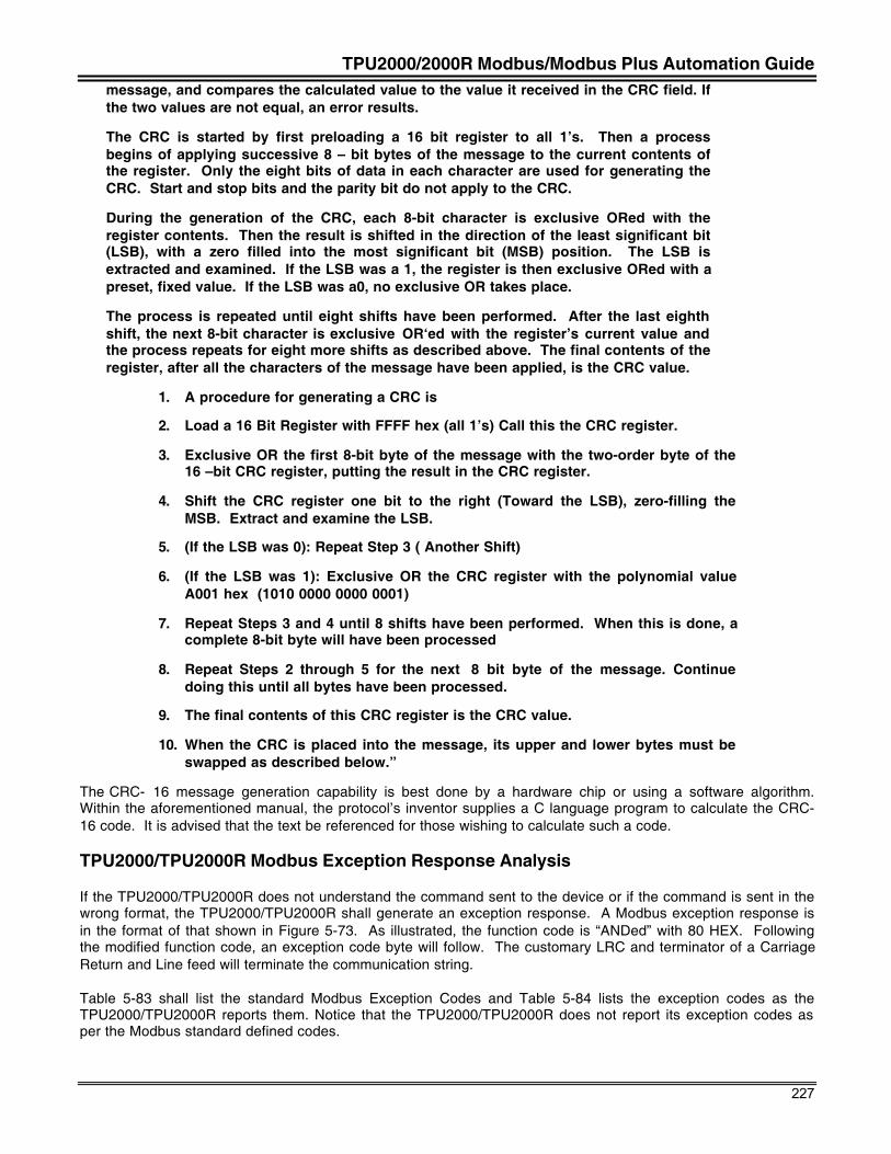
TPU2000/2000R Modbus/Modbus Plus Automation Guide
227
message, and compares the calculated value to the value it received in the CRC field. Ifthe two values are not equal, an error results.
The CRC is started by first preloading a 16 bit register to all 1’s. Then a processbegins of applying successive 8 – bit bytes of the message to the current contents ofthe register. Only the eight bits of data in each character are used for generating theCRC. Start and stop bits and the parity bit do not apply to the CRC.
During the generation of the CRC, each 8-bit character is exclusive ORed with theregister contents. Then the result is shifted in the direction of the least significant bit(LSB), with a zero filled into the most significant bit (MSB) position. The LSB isextracted and examined. If the LSB was a 1, the register is then exclusive ORed with apreset, fixed value. If the LSB was a0, no exclusive OR takes place.
The process is repeated until eight shifts have been performed. After the last eighthshift, the next 8-bit character is exclusive OR‘ed with the register’s current value andthe process repeats for eight more shifts as described above. The final contents of theregister, after all the characters of the message have been applied, is the CRC value.
1. A procedure for generating a CRC is
2. Load a 16 Bit Register with FFFF hex (all 1’s) Call this the CRC register.
3. Exclusive OR the first 8-bit byte of the message with the two-order byte of the16 –bit CRC register, putting the result in the CRC register.
4. Shift the CRC register one bit to the right (Toward the LSB), zero-filling theMSB. Extract and examine the LSB.
5. (If the LSB was 0): Repeat Step 3 ( Another Shift)
6. (If the LSB was 1): Exclusive OR the CRC register with the polynomial valueA001 hex (1010 0000 0000 0001)
7. Repeat Steps 3 and 4 until 8 shifts have been performed. When this is done, acomplete 8-bit byte will have been processed
8. Repeat Steps 2 through 5 for the next 8 bit byte of the message. Continuedoing this until all bytes have been processed.
9. The final contents of this CRC register is the CRC value.
10. When the CRC is placed into the message, its upper and lower bytes must beswapped as described below.”
The CRC- 16 message generation capability is best done by a hardware chip or using a software algorithm.Within the aforementioned manual, the protocol’s inventor supplies a C language program to calculate the CRC-16 code. It is advised that the text be referenced for those wishing to calculate such a code.
TPU2000/TPU2000R Modbus Exception Response Analysis
If the TPU2000/TPU2000R does not understand the command sent to the device or if the command is sent in thewrong format, the TPU2000/TPU2000R shall generate an exception response. A Modbus exception response isin the format of that shown in Figure 5-73. As illustrated, the function code is “ANDed” with 80 HEX. Followingthe modified function code, an exception code byte will follow. The customary LRC and terminator of a CarriageReturn and Line feed will terminate the communication string.
Table 5-83 shall list the standard Modbus Exception Codes and Table 5-84 lists the exception codes as theTPU2000/TPU2000R reports them. Notice that the TPU2000/TPU2000R does not report its exception codes asper the Modbus standard defined codes.
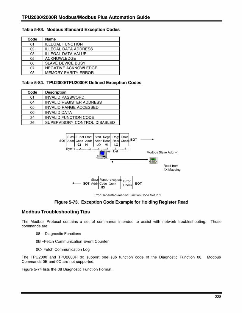
TPU2000/2000R Modbus/Modbus Plus Automation Guide
228
Table 5-83. Modbus Standard Exception Codes
Code Name01 ILLEGAL FUNCTION02 ILLEGAL DATA ADDRESS03 ILLEGAL DATA VALUE05 ACKNOWLEDGE06 SLAVE DEVICE BUSY07 NEGATIVE ACKNOWLEDGE08 MEMORY PARITY ERROR
Table 5-84. TPU2000/TPU2000R Defined Exception Codes
Code Description01 INVALID PASSWORD04 INVALID REGISTER ADDRESS05 INVALID RANGE ACCESSED06 INVALID DATA34 INVALID FUNCTION CODE36 SUPERVISORY CONTROL DISABLED
Modbus Host Modbus Slave Addr =1
Read from 4X Mapping
SlaveAddr.
Funct.Code 03
StartAddrHI
Start Addr LO
RegsRead HI
RegsRead LO
ErrorCheck EOTSOT
Byte 1 …2……..3…….4…….5……6……..7….
SlaveAddr.
Funct.Code 83
Exception Code
ErrorCheck EOTSOT
E
C
NetworkPartnerV1.0
Error Generated- msb of Function Code Set to 1
Figure 5-73. Exception Code Example for Holding Register Read
Modbus Troubleshooting Tips
The Modbus Protocol contains a set of commands intended to assist with network troubleshooting. Thosecommands are:
08 – Diagnostic Functions
0B –Fetch Communication Event Counter
0C- Fetch Communication Log
The TPU2000 and TPU2000R do support one sub function code of the Diagnostic Function 08. ModbusCommands 0B and 0C are not supported.
Figure 5-74 lists the 08 Diagnostic Function Format.
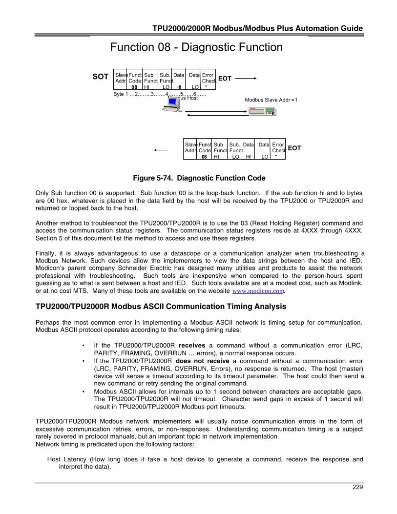
TPU2000/2000R Modbus/Modbus Plus Automation Guide
229
Function 08 - Diagnostic Function
Modbus Host
EC
Modbus Slave Addr =1
SlaveAddr.
Funct.Code 08
SubFunct.HI
Sub. Funct. LO
Data
HI
Data
LO
ErrorCheck *
EOT
Byte 1 …2……..3…….4…….5……6……
SOT
SlaveAddr.
Funct.Code 08
SubFunct.HI
Sub. Funct. LO
Data
HI
Data
LO
ErrorCheck *
EOT
Figure 5-74. Diagnostic Function Code
Only Sub function 00 is supported. Sub function 00 is the loop-back function. If the sub function hi and lo bytesare 00 hex, whatever is placed in the data field by the host will be received by the TPU2000 or TPU2000R andreturned or looped back to the host.
Another method to troubleshoot the TPU2000/TPU2000R is to use the 03 (Read Holding Register) command andaccess the communication status registers. The communication status registers reside at 4XXX through 4XXX.Section 5 of this document list the method to access and use these registers.
Finally, it is always advantageous to use a datascope or a communication analyzer when troubleshooting aModbus Network. Such devices allow the implementers to view the data strings between the host and IED.Modicon’s parent company Schneider Electric has designed many utilities and products to assist the networkprofessional with troubleshooting. Such tools are inexpensive when compared to the person-hours spentguessing as to what is sent between a host and IED. Such tools available are at a modest cost, such as Modlink,or at no cost MTS. Many of these tools are available on the website www.modicon.com.
TPU2000/TPU2000R Modbus ASCII Communication Timing Analysis
Perhaps the most common error in implementing a Modbus ASCII network is timing setup for communication.Modbus ASCII protocol operates according to the following timing rules:
• If the TPU2000/TPU2000R receives a command without a communication error (LRC,PARITY, FRAMING, OVERRUN … errors), a normal response occurs.
• If the TPU2000/TPU2000R does not receive a command without a communication error(LRC, PARITY, FRAMING, OVERRUN, Errors), no response is returned. The host (master)device will sense a timeout according to its timeout parameter. The host could then send anew command or retry sending the original command.
• Modbus ASCII allows for internals up to 1 second between characters are acceptable gaps.The TPU2000/TPU2000R will not timeout. Character send gaps in excess of 1 second willresult in TPU2000/TPU2000R Modbus port timeouts.
TPU2000/TPU2000R Modbus network implementers will usually notice communication errors in the form ofexcessive communication retries, errors, or non-responses. Understanding communication timing is a subjectrarely covered in protocol manuals, but an important topic in network implementation.Network timing is predicated upon the following factors:
Host Latency (How long does it take a host device to generate a command, receive the response andinterpret the data).
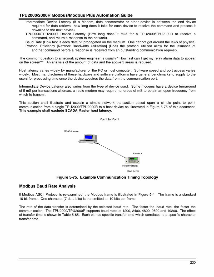
TPU2000/2000R Modbus/Modbus Plus Automation Guide
230
Intermediate Device Latency (If a Modem, data concentrator or other device is between the end devicerequired for data retrieval, how long does it take for each device to receive the command and process itdownline to the next device).
TPU2000/TPU2000R Device Latency (How long does it take for a TPU2000/TPU2000R to receive acommand, and return a response to the network).
Baud Rate (How fast is each data bit propagated on the medium. One cannot get around the laws of physics)Protocol Efficiency [Network Bandwidth Utilization] (Does the protocol utilized allow for the issuance of
another command before a response is received from an outstanding communication request).
The common question to a network system engineer is usually “ How fast can I get my relay alarm data to appearon the screen?”. An analysis of the amount of data and the above 5 areas is required.
Host latency varies widely by manufacturer or the PC or host computer. Software speed and port access varieswidely. Most manufacturers of these hardware and software platforms have general benchmarks to supply to theusers for processing time once the device acquires the data from the communication port.
Intermediate Device Latency also varies from the type of device used. Some modems have a device turnaroundof 5 mS per transactions whereas, a radio modem may require hundreds of mS to obtain an open frequency fromwhich to transmit.
This section shall illustrate and explain a simple network transaction based upon a simple point to pointcommunication from a single TPU2000/TPU2000R to a host device as illustrated in Figure 5-75 of this document.This example shall exclude SCADA Master host latency.
SCADA Master
Protective Relay
Point to Point
Slave Device
Address X
E
C
N e t w o r kPartnerV1.0
Figure 5-75. Example Communication Timing Topology
Modbus Baud Rate Analysis
If Modbus ASCII Protocol is re-examined, the Modbus frame is illustrated in Figure 5-4. The frame is a standard10 bit frame. One character (7 data bits) is transmitted as 10 bits per frame.
The rate of the data transfer is determined by the selected baud rate. The faster the baud rate, the faster thecommunication. The TPU2000/TPU2000R supports baud rates of 1200, 2400, 4800, 9600 and 19200. The effectof transfer time is shown in Table 5-85. Each bit has specific transfer time which correlates to a specific charactertransfer time.
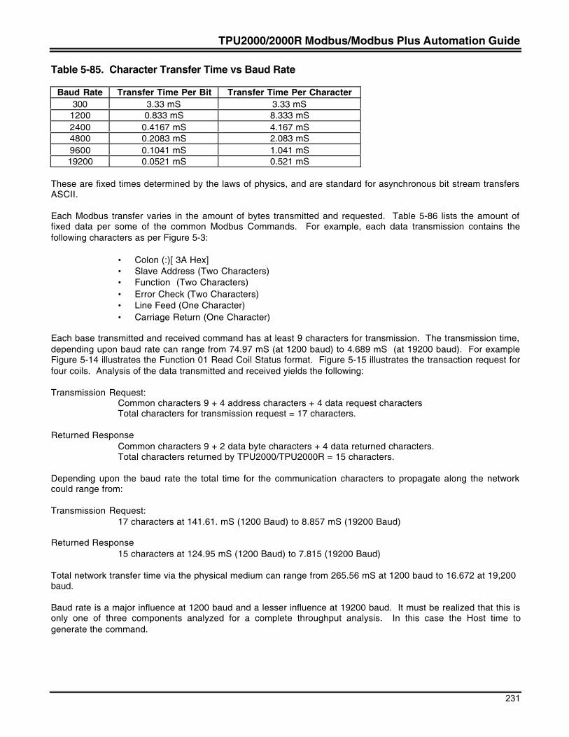
TPU2000/2000R Modbus/Modbus Plus Automation Guide
231
Table 5-85. Character Transfer Time vs Baud Rate
Baud Rate Transfer Time Per Bit Transfer Time Per Character300 3.33 mS 3.33 mS
1200 0.833 mS 8.333 mS2400 0.4167 mS 4.167 mS4800 0.2083 mS 2.083 mS9600 0.1041 mS 1.041 mS19200 0.0521 mS 0.521 mS
These are fixed times determined by the laws of physics, and are standard for asynchronous bit stream transfersASCII.
Each Modbus transfer varies in the amount of bytes transmitted and requested. Table 5-86 lists the amount offixed data per some of the common Modbus Commands. For example, each data transmission contains thefollowing characters as per Figure 5-3:
• Colon (:)[ 3A Hex]• Slave Address (Two Characters)• Function (Two Characters)• Error Check (Two Characters)• Line Feed (One Character)• Carriage Return (One Character)
Each base transmitted and received command has at least 9 characters for transmission. The transmission time,depending upon baud rate can range from 74.97 mS (at 1200 baud) to 4.689 mS (at 19200 baud). For exampleFigure 5-14 illustrates the Function 01 Read Coil Status format. Figure 5-15 illustrates the transaction request forfour coils. Analysis of the data transmitted and received yields the following:
Transmission Request:Common characters 9 + 4 address characters + 4 data request charactersTotal characters for transmission request = 17 characters.
Returned ResponseCommon characters 9 + 2 data byte characters + 4 data returned characters.Total characters returned by TPU2000/TPU2000R = 15 characters.
Depending upon the baud rate the total time for the communication characters to propagate along the networkcould range from:
Transmission Request:17 characters at 141.61. mS (1200 Baud) to 8.857 mS (19200 Baud)
Returned Response15 characters at 124.95 mS (1200 Baud) to 7.815 (19200 Baud)
Total network transfer time via the physical medium can range from 265.56 mS at 1200 baud to 16.672 at 19,200baud.
Baud rate is a major influence at 1200 baud and a lesser influence at 19200 baud. It must be realized that this isonly one of three components analyzed for a complete throughput analysis. In this case the Host time togenerate the command.
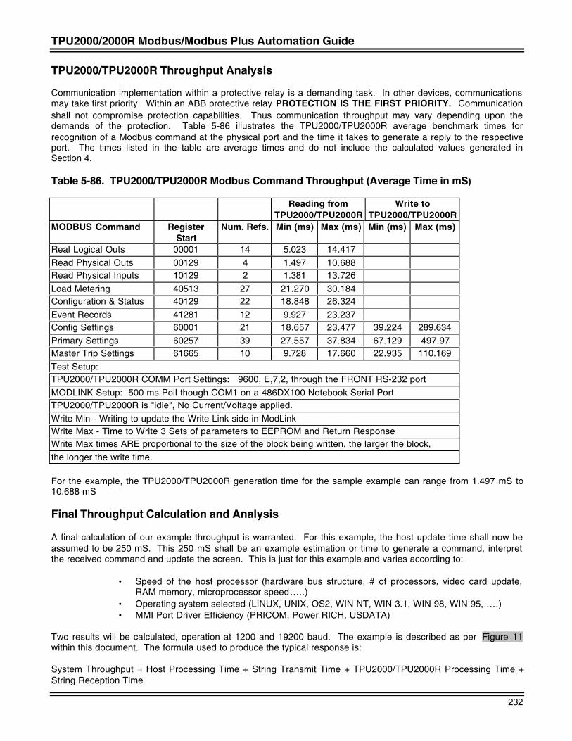
TPU2000/2000R Modbus/Modbus Plus Automation Guide
232
TPU2000/TPU2000R Throughput Analysis
Communication implementation within a protective relay is a demanding task. In other devices, communicationsmay take first priority. Within an ABB protective relay PROTECTION IS THE FIRST PRIORITY. Communicationshall not compromise protection capabilities. Thus communication throughput may vary depending upon thedemands of the protection. Table 5-86 illustrates the TPU2000/TPU2000R average benchmark times forrecognition of a Modbus command at the physical port and the time it takes to generate a reply to the respectiveport. The times listed in the table are average times and do not include the calculated values generated inSection 4.
Table 5-86. TPU2000/TPU2000R Modbus Command Throughput (Average Time in mS)
Reading fromTPU2000/TPU2000R
Write toTPU2000/TPU2000R
MODBUS Command RegisterStart
Num. Refs. Min (ms) Max (ms) Min (ms) Max (ms)
Real Logical Outs 00001 14 5.023 14.417Read Physical Outs 00129 4 1.497 10.688Read Physical Inputs 10129 2 1.381 13.726Load Metering 40513 27 21.270 30.184Configuration & Status 40129 22 18.848 26.324Event Records 41281 12 9.927 23.237Config Settings 60001 21 18.657 23.477 39.224 289.634Primary Settings 60257 39 27.557 37.834 67.129 497.97Master Trip Settings 61665 10 9.728 17.660 22.935 110.169Test Setup:TPU2000/TPU2000R COMM Port Settings: 9600, E,7,2, through the FRONT RS-232 portMODLINK Setup: 500 ms Poll though COM1 on a 486DX100 Notebook Serial PortTPU2000/TPU2000R is "idle", No Current/Voltage applied.Write Min - Writing to update the Write Link side in ModLinkWrite Max - Time to Write 3 Sets of parameters to EEPROM and Return ResponseWrite Max times ARE proportional to the size of the block being written, the larger the block,the longer the write time.
For the example, the TPU2000/TPU2000R generation time for the sample example can range from 1.497 mS to10.688 mS
Final Throughput Calculation and Analysis
A final calculation of our example throughput is warranted. For this example, the host update time shall now beassumed to be 250 mS. This 250 mS shall be an example estimation or time to generate a command, interpretthe received command and update the screen. This is just for this example and varies according to:
• Speed of the host processor (hardware bus structure, # of processors, video card update,RAM memory, microprocessor speed…..)
• Operating system selected (LINUX, UNIX, OS2, WIN NT, WIN 3.1, WIN 98, WIN 95, ….)• MMI Port Driver Efficiency (PRICOM, Power RICH, USDATA)
Two results will be calculated, operation at 1200 and 19200 baud. The example is described as per Figure 11within this document. The formula used to produce the typical response is:
System Throughput = Host Processing Time + String Transmit Time + TPU2000/TPU2000R Processing Time +String Reception Time
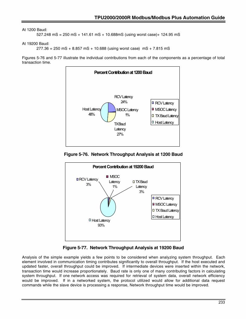
TPU2000/2000R Modbus/Modbus Plus Automation Guide
233
At 1200 Baud:527.248 mS = 250 mS + 141.61 mS + 10.688mS (using worst case)+ 124.95 mS
At 19200 Baud:277.36 = 250 mS + 8.857 mS + 10.688 (using worst case) mS + 7.815 mS
Figures 5-76 and 5-77 illustrate the individual contributions from each of the components as a percentage of totaltransaction time.
Percent Contribution at 1200 Baud
RCV Latency24%
MSOC Latency1%
TX Baud Latency
27%
Host Latency48%
RCV Latency
MSOC Latency
TX Baud Latency
Host Latency
Figure 5-76. Network Throughput Analysis at 1200 Baud
Percent Contribution at 19200 Baud
Host Latency93%
TX Baud Latency
3%
RCV Latency3%
MSOC Latency
1%
RCV Latency
MSOC Latency
TX Baud Latency
Host Latency
Figure 5-77. Network Throughput Analysis at 19200 Baud
Analysis of the simple example yields a few points to be considered when analyzing system throughput. Eachelement involved in communication timing contributes significantly to overall throughput. If the host executed andupdated faster, overall throughput could be improved. If intermediate devices were inserted within the network,transaction time would increase proportionately. Baud rate is only one of many contributing factors in calculatingsystem throughput. If one network access was required for retrieval of system data, overall network efficiencywould be improved. If in a networked system, the protocol utilized would allow for additional data requestcommands while the slave device is processing a response, Network throughput time would be improved.
TPU2000/2000R Modbus/Modbus Plus Automation Guide
234
Virtual treatises have been written on improving system throughput and data updates. This simple exampleillustrates and allows the user to calculate system throughput times. This is especially critical so that the systemuser will not be surprised with overall system response.
ABB has implemented features within the protective relay to maintain system data integrity. Latched bit status,momentary change detect are a few features implemented within the various implementations of the Modbusprotocol.
Modbus Plus Troubleshooting
Schneider Electric has designed Modbus Plus to be a very robust communication network. The publication 890USE 100 00 Version 2.0 titled Modicon Modbus Plus Network Planning and Installation Guide Copyright 1995,AEG Schneider Automation, Inc. details the method for troubleshooting a Modbus Plus network.
There is no communication analyzer for Modbus Plus to view the communication commands occurring over thenetwork. The SA 85 or PCMCIA Modbus Plus adapters have a software utility called MBP STAT which allows apersonal computer to attach to the network allowing a network professional to troubleshoot a Modbus Plusanomaly. Please reference the MBP STAT documentation for use of this valuable troubleshooting tool.
Issues common to Modbus Plus communication errors arise from the following:
1. Improper Device Termination. The manufacturer’s in-line and termination connectors must be used.Termination connectors must be used at the end of the lines for a string. The end of the string couldbe a repeater, bridge, repeater, or end device node.
2. Improper cable used. The manufacturer’s cable should be used in that it is the correct impedance,capacitance and physical wire dimensions to physically mate with the connector.
3. Improper addressing is assumed. The TPU2000/2000R ‘s address is in HEX. The Modbus Plus hostand MBP STAT uses decimal addressing. Additionally, it must be remembered that an additionalbyte must be appended to the end of the address signifying the path the host wishes to communicate.
4. Improper routing of the cable. The cable should be routed clear of high current devices and wires.Although, Modbus Plus is an industrial network, it is not recommended to route or wrap the cablearound devices (such as bus bar) which emit EMI/RFI or high current spike devices. The network is aserial network, branches, or splits are not allowed in the cabling. If such configurations arenecessary, please use fiber optics.
5. Improper grounding of the cable.
If proper care is not taken in the planning and installation of the network, the time saved on planning andinstallation is usually spent and exceeded in troubleshooting of the network. Since Modbus Plus is a serialnetwork, any loose connection, impedance mismatch, or anomaly is usually difficult to find. Cable planning andinstallation errors are usually seen as communication errors or retries seen using the MBP STAT utility. Thecable must be checked for continuity (in case of damage) and usually the cable must be disconnected and thecable sections checked.
A copy of the device troubleshooting section from the aforementioned Modbus Plus text is included for the benefitof the reader. The section covers cable continuity.
q Before checking continuity, disconnect all network cable connectors from the node devices-leave the drop cable ground lugs (ed. Note – if any since the tap and drop connectors haveground lugs whereas the dark and light grey connectors do not).to their site panel grounds.
q At any node device connector, measure the resistance between pins 2 and 3 (the signalpins), in the range of 60..80 Ω, which include the cable wire resistance.
q At each node device connector, check for an open circuit between pin 2 (a signal pin) and pin1 (the shield pin); then check between pin 3 (a signal pin) and pin 1 – an open circuit shouldexist for both checks.
q At each connector, check the continuity between pin 1 and the plant ground point on the localsite panel or frame – direct continuity should be present.
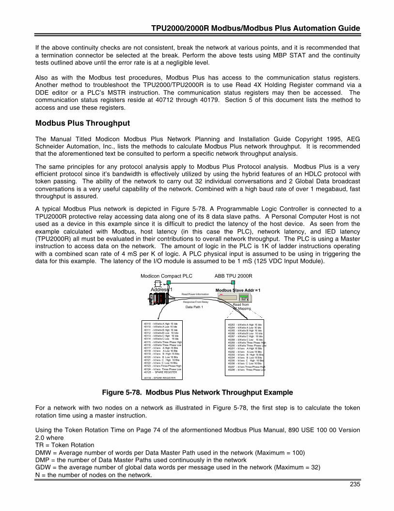
TPU2000/2000R Modbus/Modbus Plus Automation Guide
235
If the above continuity checks are not consistent, break the network at various points, and it is recommended thata termination connector be selected at the break. Perform the above tests using MBP STAT and the continuitytests outlined above until the error rate is at a negligible level.
Also as with the Modbus test procedures, Modbus Plus has access to the communication status registers.Another method to troubleshoot the TPU2000/TPU2000R is to use Read 4X Holding Register command via aDDE editor or a PLC’s MSTR instruction. The communication status registers may then be accessed. Thecommunication status registers reside at 40712 through 40179. Section 5 of this document lists the method toaccess and use these registers.
Modbus Plus Throughput
The Manual Titled Modicon Modbus Plus Network Planning and Installation Guide Copyright 1995, AEGSchneider Automation, Inc., lists the methods to calculate Modbus Plus network throughput. It is recommendedthat the aforementioned text be consulted to perform a specific network throughput analysis.
The same principles for any protocol analysis apply to Modbus Plus Protocol analysis. Modbus Plus is a veryefficient protocol since it’s bandwidth is effectively utilized by using the hybrid features of an HDLC protocol withtoken passing. The ability of the network to carry out 32 individual conversations and 2 Global Data broadcastconversations is a very useful capability of the network. Combined with a high baud rate of over 1 megabaud, fastthroughput is assured.
A typical Modbus Plus network is depicted in Figure 5-78. A Programmable Logic Controller is connected to aTPU2000R protective relay accessing data along one of its 8 data slave paths. A Personal Computer Host is notused as a device in this example since it is difficult to predict the latency of the host device. As seen from theexample calculated with Modbus, host latency (in this case the PLC), network latency, and IED latency(TPU2000R) all must be evaluated in their contributions to overall network throughput. The PLC is using a Masterinstruction to access data on the network. The amount of logic in the PLC is 1K of ladder instructions operatingwith a combined scan rate of 4 mS per K of logic. A PLC physical input is assumed to be using in triggering thedata for this example. The latency of the I/O module is assumed to be 1 mS (125 VDC Input Module).
Address 1
EC
Modbus Slave Addr =1
Read from 4X Mapping
40283 - kWatts A High 16 bits40284 - kWatts A Low 16 bits40285 - kWatts B High 16 bits40286 - kWatts B Low 16 bits40287 - kWatts C High 16 bits40288 - kWatts C Low 16 bits40289 - kWatts Three Phase High40290 - kWatts Three Phase Low40291 - kVars A High 16 Bits40292 - kVars A Low 16 Bits40293 - kVars B High 16 Bits40294 - kVars B Low 16 Bits40295 - kVars C High 16 Bits40296 - kVars C Low 16 Bits40297 - kVars Three Phase High40298 - kVars Three Phase Low
Read Power Information
Response From Relay
40110 - kWatts A High 16 bits40110 - kWatts A Low 16 bits40111 - kWatts B High 16 bits40112 - kWatts B Low 16 bits40113 - kWatts C High 16 bits40114 - kWatts C Low 16 bits40115 - kWatts Three Phase High40116 - kWatts Three Phase Low40117 - kVars A High 16 Bits40118 - kVars A Low 16 Bits40119 - kVars B High 16 Bits40120 - kVars B Low 16 Bits40121 - kVars C High 16 Bits40122 - kVars C Low 16 Bits40123 - kVars Three Phase High40124 - kVars Three Phase Low40125 - SPARE REGISTER :40139 - SPARE REGISTER
Modicon Compact PLC ABB TPU 2000RMSTR
Data Path 1
Figure 5-78. Modbus Plus Network Throughput Example
For a network with two nodes on a network as illustrated in Figure 5-78, the first step is to calculate the tokenrotation time using a master instruction.
Using the Token Rotation Time on Page 74 of the aformentioned Modbus Plus Manual, 890 USE 100 00 Version2.0 whereTR = Token RotationDMW = Average number of words per Data Master Path used in the network (Maximum = 100)DMP = the number of Data Master Paths used continuously in the networkGDW = the average number of global data words per message used in the network (Maximum = 32)N = the number of nodes on the network.
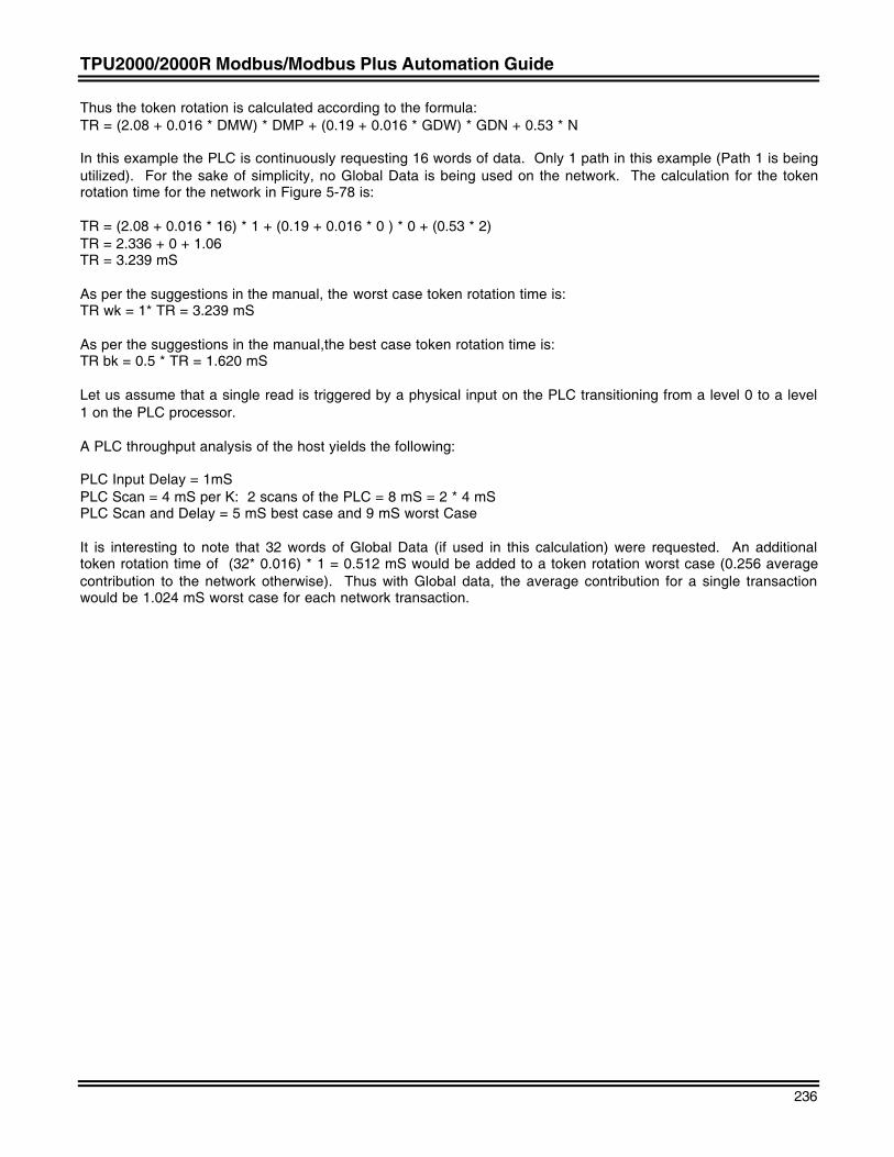
TPU2000/2000R Modbus/Modbus Plus Automation Guide
236
Thus the token rotation is calculated according to the formula:TR = (2.08 + 0.016 * DMW) * DMP + (0.19 + 0.016 * GDW) * GDN + 0.53 * N
In this example the PLC is continuously requesting 16 words of data. Only 1 path in this example (Path 1 is beingutilized). For the sake of simplicity, no Global Data is being used on the network. The calculation for the tokenrotation time for the network in Figure 5-78 is:
TR = (2.08 + 0.016 * 16) * 1 + (0.19 + 0.016 * 0 ) * 0 + (0.53 * 2)TR = 2.336 + 0 + 1.06TR = 3.239 mS
As per the suggestions in the manual, the worst case token rotation time is:TR wk = 1* TR = 3.239 mS
As per the suggestions in the manual,the best case token rotation time is:TR bk = 0.5 * TR = 1.620 mS
Let us assume that a single read is triggered by a physical input on the PLC transitioning from a level 0 to a level1 on the PLC processor.
A PLC throughput analysis of the host yields the following:
PLC Input Delay = 1mSPLC Scan = 4 mS per K: 2 scans of the PLC = 8 mS = 2 * 4 mSPLC Scan and Delay = 5 mS best case and 9 mS worst Case
It is interesting to note that 32 words of Global Data (if used in this calculation) were requested. An additionaltoken rotation time of (32* 0.016) * 1 = 0.512 mS would be added to a token rotation worst case (0.256 averagecontribution to the network otherwise). Thus with Global data, the average contribution for a single transactionwould be 1.024 mS worst case for each network transaction.
TPU2000/2000R Modbus/Modbus Plus Automation Guide
237
Appendix A - TPU2000 Protocol Command Set
Revision 3.1
1 Revision History
Revision Date Author Description3.1 04/07/98 VAB 3-4-11: maximum CT ratio was 2000 for messages 2/1-4/2.
Maximum VT ratio was 2000 for message 20/1-20/2.
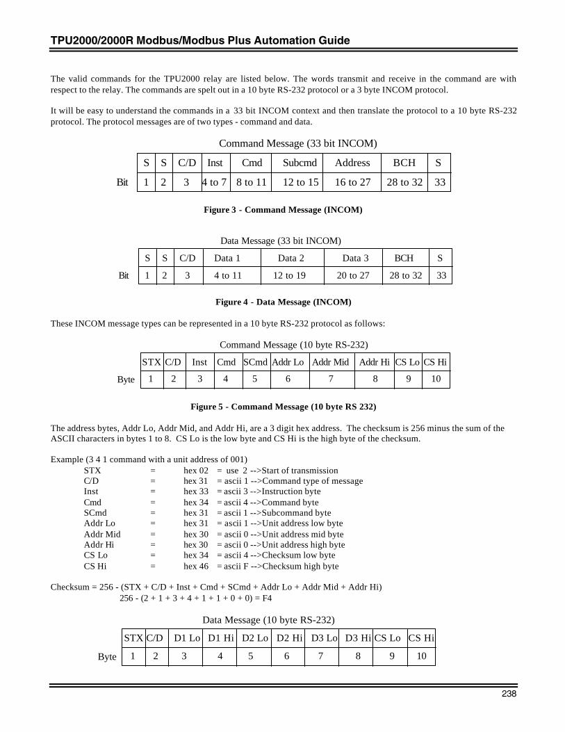
TPU2000/2000R Modbus/Modbus Plus Automation Guide
238
The valid commands for the TPU2000 relay are listed below. The words transmit and receive in the command are withrespect to the relay. The commands are spelt out in a 10 byte RS-232 protocol or a 3 byte INCOM protocol.
It will be easy to understand the commands in a 33 bit INCOM context and then translate the protocol to a 10 byte RS-232protocol. The protocol messages are of two types - command and data.
S S C/D Inst Cmd AddressSubcmd BCH S
1 2 3 4 to 7 8 to 11 12 to 15 16 to 27 28 to 32 33Bit
Command Message (33 bit INCOM)
Figure 3 - Command Message (INCOM)
Figure 4 - Data Message (INCOM)
These INCOM message types can be represented in a 10 byte RS-232 protocol as follows:
STX C/D
1 2 3Byte
Command Message (10 byte RS-232)
Inst Cmd SCmd Addr Lo Addr Mid Addr Hi CS Lo CS Hi
4 5 6 7 8 9 10
Figure 5 - Command Message (10 byte RS 232)
The address bytes, Addr Lo, Addr Mid, and Addr Hi, are a 3 digit hex address. The checksum is 256 minus the sum of theASCII characters in bytes 1 to 8. CS Lo is the low byte and CS Hi is the high byte of the checksum.
Example (3 4 1 command with a unit address of 001)STX = hex 02 = use 2 -->Start of transmissionC/D = hex 31 = ascii 1 -->Command type of messageInst = hex 33 = ascii 3 -->Instruction byteCmd = hex 34 = ascii 4 -->Command byteSCmd = hex 31 = ascii 1 -->Subcommand byteAddr Lo = hex 31 = ascii 1 -->Unit address low byteAddr Mid = hex 30 = ascii 0 -->Unit address mid byteAddr Hi = hex 30 = ascii 0 -->Unit address high byteCS Lo = hex 34 = ascii 4 -->Checksum low byteCS Hi = hex 46 = ascii F -->Checksum high byte
Checksum = 256 - (STX + C/D + Inst + Cmd + SCmd + Addr Lo + Addr Mid + Addr Hi) 256 - (2 + 1 + 3 + 4 + 1 + 1 + 0 + 0) = F4
S S C/D BCH S
1 2 3 28 to 32 33Bit
Data Message (33 bit INCOM)
Data 1 Data 2 Data 3
4 to 11 12 to 19 20 to 27
STX C/D
1 2 3Byte
Data Message (10 byte RS-232)
CS Lo CS Hi
4 5 6 7 8 9 10
D1 Lo D1 Hi D2 Lo D2 Hi D3 Lo D3 Hi
TPU2000/2000R Modbus/Modbus Plus Automation Guide
239
Figure 6 - Data Message (10 byte RS 232)
Where D1 Lo is the low nibble of the first data byte and D1 Hi is the high nibble of the first data byte, D2 Lo is the lownibble of the second data byte and D2 Hi is the high nibble of the second data byte, and D3 Lo is the low nibble of the thirddata byte and D3 Hi is the high nibble of the third data byte.
The checksum is 256 minus the sum of the ASCII characters in bytes 1 to 8. CS Lo is the low byte and CS Hi is the highbyte of the checksum.
Example (3 data bytes, ascii characters 4, 8, and 7)STX = hex 2 --> Start of transmissionC/D = hex 0 --> Data type of messageD1 Lo = hex 4 --> Data 1 low byteD1 Hi = hex 3 --> Data 1 high byteD2 Lo = hex 8 --> Data 2 low byteD2 Hi = hex 3 --> Data 2 high byteD3 Lo = hex 7 --> Data 3 low byteD3 Hi = hex 3 --> Data 3 high byteCS Lo = hex 2 --> Checksum low byteCS Hi = hex E --> Checksum high byte
The three data bytes translate to:Data 1 = 34 --> ascii 4Data 2 = 38 --> ascii 8Data 3 = 37 --> ascii 7
Checksum = 256 - (STX + C/D + D1L + D1H + D2L + D2H + D3L + D3H) 256 - (2 + 0 + 4 + 3 + 8 + 3 + 7 + 3) = E2
Transmission and reception convention
To acknowledge successful receipt of a message, an ACK is transmitted. The three byte message packet is 0x000013. For anunsuccessful reception, ie. a checksum error or an error in command processing, a NACK is transmitted. The three bytemessage packet is 0x100013.
The commands for the TPU2000 relay can be catagorized into three basic types according to the response that is expected bythe master. When a command or data is received, the TPU2000 must acknowledge if the reception was successful.
1-Simple Commands: A simple command directs the TPU2000 to perform specific actions. After the successful completionof these actions, the TPU2000 transmits an ACK as seen below.
Master DPU2000Command
ACK
Figure 7 - Simple Command Communication Flow
2-Upload Data This type of command requests the TPU2000 to transmit specific data. The proper transmission of this datais the TPU2000 acknowledge of this type of command as seen below.
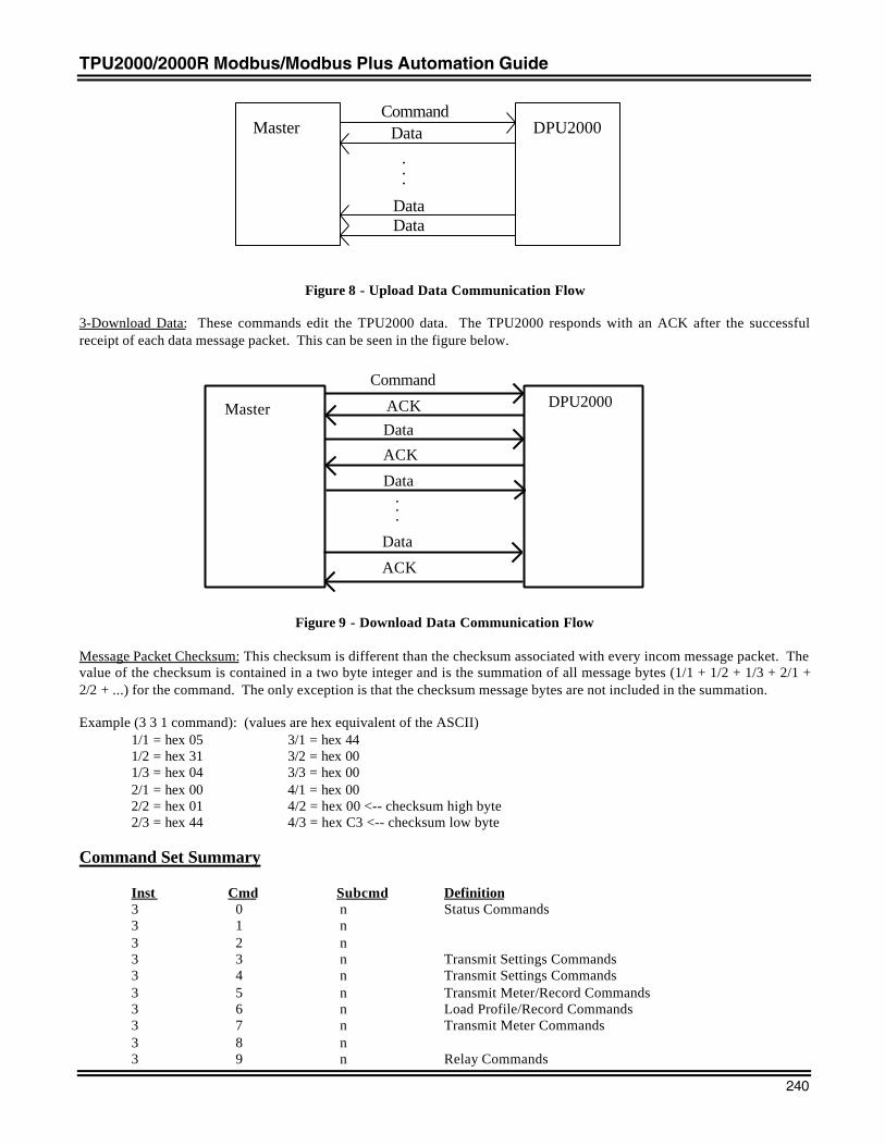
TPU2000/2000R Modbus/Modbus Plus Automation Guide
240
Figure 8 - Upload Data Communication Flow
3-Download Data: These commands edit the TPU2000 data. The TPU2000 responds with an ACK after the successfulreceipt of each data message packet. This can be seen in the figure below.
Figure 9 - Download Data Communication Flow
Message Packet Checksum: This checksum is different than the checksum associated with every incom message packet. Thevalue of the checksum is contained in a two byte integer and is the summation of all message bytes (1/1 + 1/2 + 1/3 + 2/1 +2/2 + ...) for the command. The only exception is that the checksum message bytes are not included in the summation.
Example (3 3 1 command): (values are hex equivalent of the ASCII)1/1 = hex 05 3/1 = hex 441/2 = hex 31 3/2 = hex 001/3 = hex 04 3/3 = hex 002/1 = hex 00 4/1 = hex 002/2 = hex 01 4/2 = hex 00 <-- checksum high byte2/3 = hex 44 4/3 = hex C3 <-- checksum low byte
Command Set Summary
Inst Cmd Subcmd Definition3 0 n Status Commands3 1 n3 2 n3 3 n Transmit Settings Commands3 4 n Transmit Settings Commands3 5 n Transmit Meter/Record Commands3 6 n Load Profile/Record Commands3 7 n Transmit Meter Commands3 8 n3 9 n Relay Commands
MasterCommand
Data
DataData
.
..
DPU2000
Master
Command
Data
Data
Data
..
.
ACK
ACK
ACK DPU2000
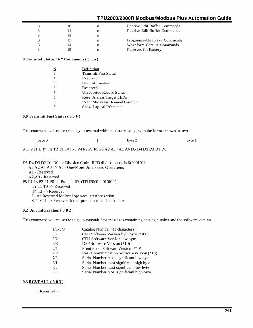
TPU2000/2000R Modbus/Modbus Plus Automation Guide
241
3 10 n Receive Edit Buffer Commands3 11 n Receive Edit Buffer Commands3 12 n3 13 n Programmable Curve Commands3 14 n Waveform Capture Commands3 15 n Reserved for Factory
0 Transmit Status "N" Commands ( 3 0 n )
N Definition 0 Transmit Fast Status 1 Reserved 2 Unit Information 3 Reserved 4 Unreported Record Status 5 Reset Alarms/Target LEDs 6 Reset Max/Min Demand Currents 7 Show Logical I/O status
0.0 Transmit Fast Status ( 3 0 0 )
This command will cause the relay to respond with one data message with the format shown below:
byte 3 | byte 2 | byte 1 ST2 ST1 L T4 T3 T2 T1 T0 | P5 P4 P3 P2 P1 P0 A3 A2 | A1 A0 D5 D4 D3 D2 D1 D0
D5 D4 D3 D2 D1 D0 => Division Code . RTD division code is 5(000101) A3 A2 A1 A0 => A0 - One/More Unreported Operations A1 - Reserved A2,A3 - ReservedP5 P4 P3 P2 P1 P0 => Product ID. (TPU2000 = 010011) T2 T1 T0 => Reserved T4 T3 => Reserved L => Reserved for local operator interface action. ST2 ST1 => Reserved for corporate standard status bits.
0.2 Unit Information ( 3 0 2 )
This command will cause the relay to transmit data messages containing catalog number and the software version.
1/1-5/3 Catalog Number (18 characters)6/1 CPU Software Version high byte (*100)6/2 CPU Software Version low byte6/3 DSP Software Version (*10)7/1 Front Panel Software Version (*10)7/2 Rear Communication Software version (*10)7/3 Serial Number most significant low byte8/1 Serial Number least significant high byte8/2 Serial Number least significant low byte8/3 Serial Number most significant high byte
0.3 RCVDALL ( 3 0 3 )
- Reserved -
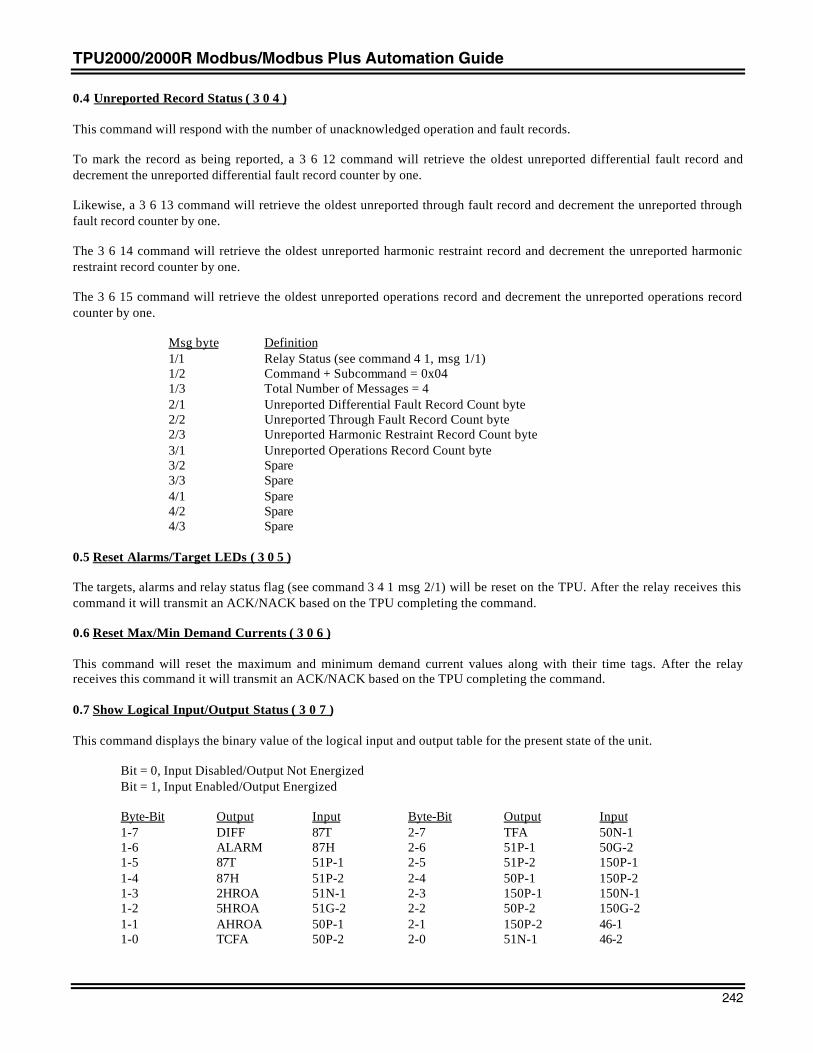
TPU2000/2000R Modbus/Modbus Plus Automation Guide
242
0.4 Unreported Record Status ( 3 0 4 )
This command will respond with the number of unacknowledged operation and fault records.
To mark the record as being reported, a 3 6 12 command will retrieve the oldest unreported differential fault record anddecrement the unreported differential fault record counter by one.
Likewise, a 3 6 13 command will retrieve the oldest unreported through fault record and decrement the unreported throughfault record counter by one.
The 3 6 14 command will retrieve the oldest unreported harmonic restraint record and decrement the unreported harmonicrestraint record counter by one.
The 3 6 15 command will retrieve the oldest unreported operations record and decrement the unreported operations recordcounter by one.
Msg byte Definition1/1 Relay Status (see command 4 1, msg 1/1)1/2 Command + Subcommand = 0x041/3 Total Number of Messages = 42/1 Unreported Differential Fault Record Count byte2/2 Unreported Through Fault Record Count byte2/3 Unreported Harmonic Restraint Record Count byte3/1 Unreported Operations Record Count byte3/2 Spare3/3 Spare4/1 Spare4/2 Spare4/3 Spare
0.5 Reset Alarms/Target LEDs ( 3 0 5 )
The targets, alarms and relay status flag (see command 3 4 1 msg 2/1) will be reset on the TPU. After the relay receives thiscommand it will transmit an ACK/NACK based on the TPU completing the command.
0.6 Reset Max/Min Demand Currents ( 3 0 6 )
This command will reset the maximum and minimum demand current values along with their time tags. After the relayreceives this command it will transmit an ACK/NACK based on the TPU completing the command.
0.7 Show Logical Input/Output Status ( 3 0 7 )
This command displays the binary value of the logical input and output table for the present state of the unit.
Bit = 0, Input Disabled/Output Not EnergizedBit = 1, Input Enabled/Output Energized
Byte-Bit Output Input Byte-Bit Output Input1-7 DIFF 87T 2-7 TFA 50N-11-6 ALARM 87H 2-6 51P-1 50G-21-5 87T 51P-1 2-5 51P-2 150P-11-4 87H 51P-2 2-4 50P-1 150P-21-3 2HROA 51N-1 2-3 150P-1 150N-11-2 5HROA 51G-2 2-2 50P-2 150G-21-1 AHROA 50P-1 2-1 150P-2 46-11-0 TCFA 50P-2 2-0 51N-1 46-2
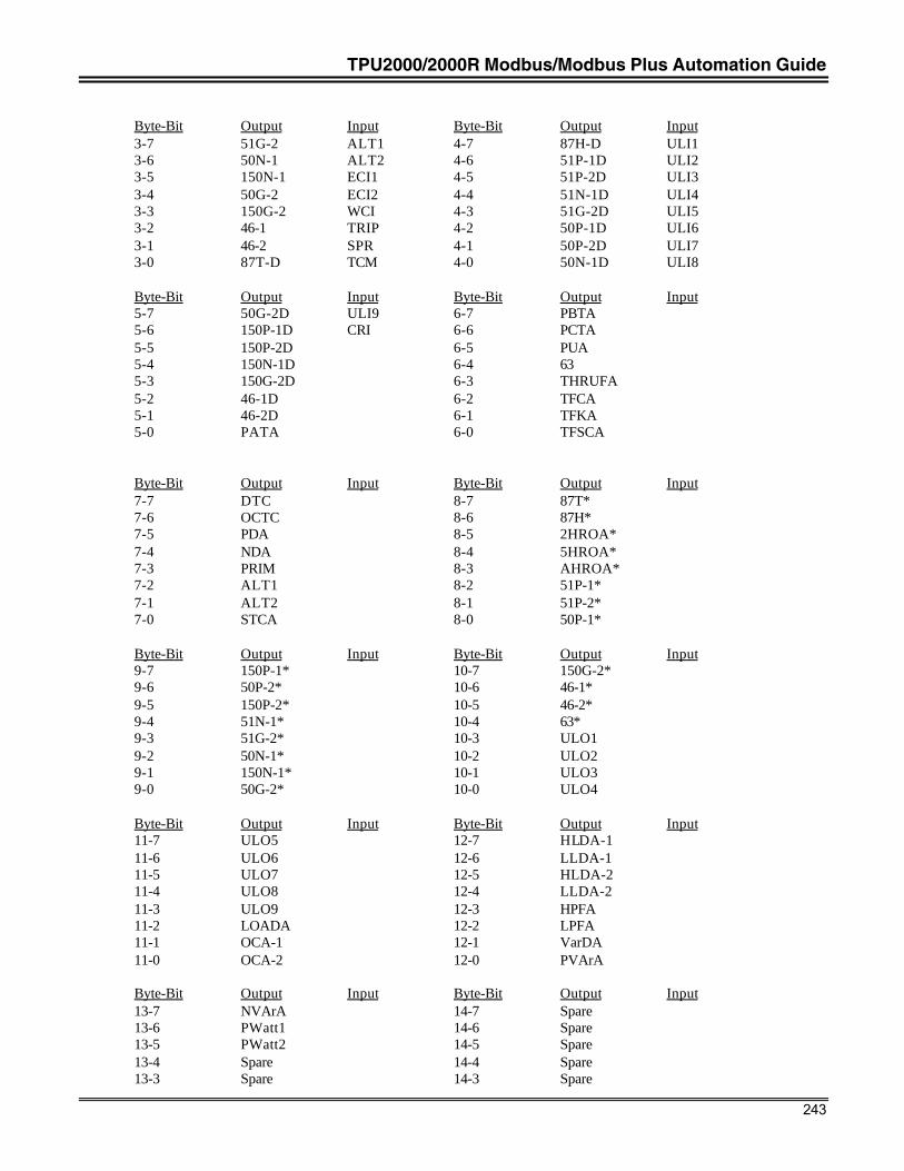
TPU2000/2000R Modbus/Modbus Plus Automation Guide
243
Byte-Bit Output Input Byte-Bit Output Input3-7 51G-2 ALT1 4-7 87H-D ULI13-6 50N-1 ALT2 4-6 51P-1D ULI23-5 150N-1 ECI1 4-5 51P-2D ULI33-4 50G-2 ECI2 4-4 51N-1D ULI43-3 150G-2 WCI 4-3 51G-2D ULI53-2 46-1 TRIP 4-2 50P-1D ULI63-1 46-2 SPR 4-1 50P-2D ULI73-0 87T-D TCM 4-0 50N-1D ULI8
Byte-Bit Output Input Byte-Bit Output Input5-7 50G-2D ULI9 6-7 PBTA5-6 150P-1D CRI 6-6 PCTA5-5 150P-2D 6-5 PUA5-4 150N-1D 6-4 635-3 150G-2D 6-3 THRUFA5-2 46-1D 6-2 TFCA5-1 46-2D 6-1 TFKA5-0 PATA 6-0 TFSCA
Byte-Bit Output Input Byte-Bit Output Input7-7 DTC 8-7 87T*7-6 OCTC 8-6 87H*7-5 PDA 8-5 2HROA*7-4 NDA 8-4 5HROA*7-3 PRIM 8-3 AHROA*7-2 ALT1 8-2 51P-1*7-1 ALT2 8-1 51P-2*7-0 STCA 8-0 50P-1*
Byte-Bit Output Input Byte-Bit Output Input9-7 150P-1* 10-7 150G-2*9-6 50P-2* 10-6 46-1*9-5 150P-2* 10-5 46-2*9-4 51N-1* 10-4 63*9-3 51G-2* 10-3 ULO19-2 50N-1* 10-2 ULO29-1 150N-1* 10-1 ULO39-0 50G-2* 10-0 ULO4
Byte-Bit Output Input Byte-Bit Output Input11-7 ULO5 12-7 HLDA-111-6 ULO6 12-6 LLDA-111-5 ULO7 12-5 HLDA-211-4 ULO8 12-4 LLDA-211-3 ULO9 12-3 HPFA11-2 LOADA 12-2 LPFA11-1 OCA-1 12-1 VarDA11-0 OCA-2 12-0 PVArA
Byte-Bit Output Input Byte-Bit Output Input13-7 NVArA 14-7 Spare13-6 PWatt1 14-6 Spare13-5 PWatt2 14-5 Spare13-4 Spare 14-4 Spare13-3 Spare 14-3 Spare
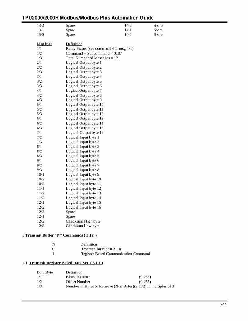
TPU2000/2000R Modbus/Modbus Plus Automation Guide
244
13-2 Spare 14-2 Spare13-1 Spare 14-1 Spare13-0 Spare 14-0 Spare
Msg byte Definition1/1 Relay Status (see command 4 1, msg 1/1)1/2 Command + Subcommand = 0x071/3 Total Number of Messages = 122/1 Logical Output byte 12/2 Logical Output byte 22/3 Logical Output byte 33/1 Logical Output byte 43/2 Logical Output byte 53/3 Logical Output byte 64/1 Logical Output byte 74/2 Logical Output byte 84/3 Logical Output byte 95/1 Logical Output byte 105/2 Logical Output byte 115/3 Logical Output byte 126/1 Logical Output byte 136/2 Logical Output byte 146/3 Logical Output byte 157/1 Logical Output byte 167/2 Logical Input byte 17/3 Logical Input byte 28/1 Logical Input byte 38/2 Logical Input byte 48/3 Logical Input byte 59/1 Logical Input byte 69/2 Logical Input byte 79/3 Logical Input byte 810/1 Logical Input byte 910/2 Logical Input byte 1010/3 Logical Input byte 1111/1 Logical Input byte 1211/2 Logical Input byte 1311/3 Logical Input byte 1412/1 Logical Input byte 1512/2 Logical Input byte 1612/3 Spare12/1 Spare12/2 Checksum High byte12/3 Checksum Low byte
1 Transmit Buffer "N" Commands ( 3 1 n )
N Definition 0 Reserved for repeat 3 1 n 1 Register Based Communication Command
1.1 Transmit Register Based Data Set ( 3 1 1 )
Data Byte Definition1/1 Block Number (0-255)1/2 Offset Number (0-255)1/3 Number of Bytes to Retrieve (NumBytes)(3-132) in multiples of 3
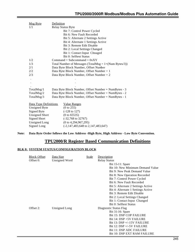
TPU2000/2000R Modbus/Modbus Plus Automation Guide
245
Msg Byte Definition1/1 Relay Status Byte
Bit 7: Control Power CycledBit 6: New Fault RecordedBit 5: Alternate 2 Settings ActiveBit 4: Alternate 1 Settings ActiveBit 3: Remote Edit DisableBit 2: Local Settings ChangedBit 1: Contact Input ChnagedBit 0: Selftest Status
1/2 Command + Subcommand = 0xXY1/3 Total Number of Messages (TotalMsg = 1+(Num Bytes/3))2/1 Data Byte Block Number, Offset Number2/2 Data Byte Block Number, Offset Number + 12/3 Data Byte Block Number, Offset Number + 2 . . . . . .TotalMsg/1 Data Byte Block Number, Offset Number + NumBytes - 3TotalMsg/2 Data Byte Block Number, Offset Number + NumBytes - 2TotalMsg/3 Data Byte Block Number, Offset Number + NumBytes - 1
Data Type Definitions Value RangesUnsigned Byte (0 to 255)Signed Byte (-128 to 127)Unsigned Short (0 to 65535)Signed Short (-32,768 to 32767)Unsigned Long (0 to 4,294,967,295)Signed Long (-2,147,483,648 to 2,147,483,647)
Note: Data Byte Order follows the Low Address -High Byte, High Address - Low Byte Convention.
TPU2000/R Register Based Communication Definitions
BLK 0: SYSTEM STATUS/CONFIGURATION BLOCK
Block Offset Data Size Scale DescriptionOffset 0: Unsigned Word Relay Status
Bit 15-11: SpareBit 10: New Minimum Demand ValueBit 9: New Peak Demand ValueBit 8: New Operation RecordedBit 7: Control Power CycledBit 6: New Fault RecordedBit 5: Alternate 2 Settings ActiveBit 4: Alternate 1 Settings ActiveBit 3: Remote Edit DisableBit 2: Local Settings ChangedBit 1: Contact Input ChangedBit 0: Selftest Status
Offset 2: Unsigned Long Diagnostic Status FlagBit 31-16: SpareBit 15: DSP COP FAILUREBit 14: DSP +5V FAILUREBit 13: DSP +/-15V FAILUREBit 12: DSP +/-5V FAILUREBit 11: DSP ADC FAILUREBit 10: DSP EXT RAM FAILURE
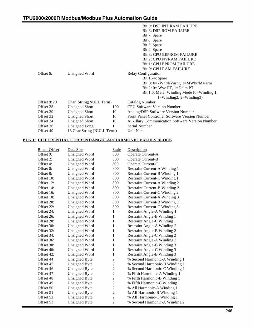
TPU2000/2000R Modbus/Modbus Plus Automation Guide
246
Bit 9: DSP INT RAM FAILUREBit 8: DSP ROM FAILUREBit 7: SpareBit 6: SpareBit 5: SpareBit 4: SpareBit 3: CPU EEPROM FAILUREBit 2: CPU NVRAM FAILUREBit 1: CPU EPROM FAILUREBit 0: CPU RAM FAILURE
Offset 6: Unsigned Word Relay ConfigurationBit 15-4: SpareBit 3: 0=kWhr/kVarhr, 1=MWhr/MVarhrBit 2: 0= Wye PT, 1=Delta PTBit 1,0: Meter Winding Mode (0=Winding 1,
1=Winding2, 2=Winding3)Offset 8: 20 Char String(NULL Term) Catalog NumberOffset 28: Unsigned Short 100 CPU Software Version NumberOffset 30: Unsigned Short 10 Analog/DSP Software Version NumberOffset 32: Unsigned Short 10 Front Panel Controller Software Version NumberOffset 34: Unsigned Short 10 Auxillary Communication Software Version NumberOffset 36: Unsigned Long 1 Serial NumberOffset 40: 18 Char String (NULL Term) Unit Name
BLK 1: DIFFERENTIAL CURRENT/ANGULAR/HARMONIC VALUES BLOCK
Block Offset Data Size Scale DescriptionOffset 0: Unsigned Word 800 Operate Current-AOffset 2: Unsigned Word 800 Operate Current-BOffset 4: Unsigned Word 800 Operate Current-COffset 6: Unsigned Word 800 Restraint Current-A Winding 1Offset 8: Unsigned Word 800 Restraint Current-B Winding 1Offset 10: Unsigned Word 800 Restraint Current-C Winding 1Offset 12: Unsigned Word 800 Restraint Current-A Winding 2Offset 14: Unsigned Word 800 Restraint Current-B Winding 2Offset 16: Unsigned Word 800 Restraint Current-C Winding 2Offset 18: Unsigned Word 800 Restraint Current-A Winding 3Offset 20: Unsigned Word 800 Restraint Current-B Winding 3Offset 22: Unsigned Word 800 Restraint Current-C Winding 3Offset 24: Unsigned Word 1 Restraint Angle-A Winding 1Offset 26: Unsigned Word 1 Restraint Angle-B Winding 1Offset 28: Unsigned Word 1 Restraint Angle-C Winding 1Offset 30: Unsigned Word 1 Restraint Angle-A Winding 2Offset 32: Unsigned Word 1 Restraint Angle-B Winding 2Offset 34: Unsigned Word 1 Restraint Angle-C Winding 2Offset 36: Unsigned Word 1 Restraint Angle-A Winding 3Offset 38: Unsigned Word 1 Restraint Angle-B Winding 3Offset 40: Unsigned Word 1 Restraint Angle-C Winding 3Offset 42: Unsigned Word 1 Restraint Angle-B Winding 3Offset 44: Unsigned Byte 2 % Second Harmonic-A Winding 1Offset 45: Unsigned Byte 2 % Second Harmonic-B Winding 1Offset 46: Unsigned Byte 2 % Second Harmonic-C Winding 1Offset 47: Unsigned Byte 2 % Fifth Harmonic-A Winding 1Offset 48: Unsigned Byte 2 % Fifth Harmonic-B Winding 1Offset 49: Unsigned Byte 2 % Fifth Harmonic-C Winding 1Offset 50: Unsigned Byte 2 % All Harmonic-A Winding 1Offset 51: Unsigned Byte 2 % All Harmonic-B Winding 1Offset 52: Unsigned Byte 2 % All Harmonic-C Winding 1Offset 53: Unsigned Byte 2 % Second Harmonic-A Winding 2
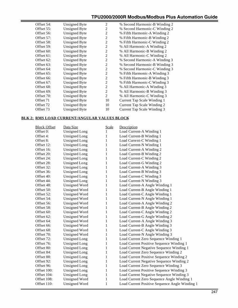
TPU2000/2000R Modbus/Modbus Plus Automation Guide
247
Offset 54: Unsigned Byte 2 % Second Harmonic-B Winding 2Offset 55: Unsigned Byte 2 % Second Harmonic-C Winding 2Offset 56: Unsigned Byte 2 % Fifth Harmonic-A Winding 2Offset 57: Unsigned Byte 2 % Fifth Harmonic-B Winding 2Offset 58: Unsigned Byte 2 % Fifth Harmonic-C Winding 2Offset 59: Unsigned Byte 2 % All Harmonic-A Winding 2Offset 60: Unsigned Byte 2 % All Harmonic-B Winding 2Offset 61: Unsigned Byte 2 % All Harmonic-C Winding 2Offset 62: Unsigned Byte 2 % Second Harmonic-A Winding 3Offset 63: Unsigned Byte 2 % Second Harmonic-B Winding 3Offset 64: Unsigned Byte 2 % Second Harmonic-C Winding 3Offset 65: Unsigned Byte 2 % Fifth Harmonic-A Winding 3Offset 66: Unsigned Byte 2 % Fifth Harmonic-B Winding 3Offset 67: Unsigned Byte 2 % Fifth Harmonic-C Winding 3Offset 68: Unsigned Byte 2 % All Harmonic-A Winding 3Offset 69: Unsigned Byte 2 % All Harmonic-B Winding 3Offset 70: Unsigned Byte 2 % All Harmonic-C Winding 3Offset 71 Unsigned Byte 10 Current Tap Scale Winding 1Offset 72 Unsigned Byte 10 Current Tap Scale Winding 2Offset 73 Unsigned Byte 10 Current Tap Scale Winding 3
BLK 2: RMS LOAD CURRENT/ANGULAR VALUES BLOCK
Block Offset Data Size Scale DescriptionOffset 0: Unsigned Long 1 Load Current-A Winding 1Offset 4: Unsigned Long 1 Load Current-B Winding 1
Offset 8: Unsigned Long 1 Load Current-C Winding 1Offset 12: Unsigned Long 1 Load Current-N Winding 1Offset 16: Unsigned Long 1 Load Current-A Winding 2Offset 20: Unsigned Long 1 Load Current-B Winding 2
Offset 24: Unsigned Long 1 Load Current-C Winding 2Offset 28: Unsigned Long 1 Load Current-G Winding 2Offset 32: Unsigned Long 1 Load Current-A Winding 3Offset 36: Unsigned Long 1 Load Current-B Winding 3
Offset 40: Unsigned Long 1 Load Current-C Winding 3Offset 44: Unsigned Long 1 Load Current-N Winding 3Offset 48: Unsigned Word 1 Load Current-A Angle Winding 1Offset 50: Unsigned Word 1 Load Current-B Angle Winding 1Offset 52: Unsigned Word 1 Load Current-C Angle Winding 1Offset 54: Unsigned Word 1 Load Current-N Angle Winding 1Offset 56: Unsigned Word 1 Load Current-A Angle Winding 2Offset 58: Unsigned Word 1 Load Current-B Angle Winding 2Offset 60: Unsigned Word 1 Load Current-C Angle Winding 2Offset 62: Unsigned Word 1 Load Current-G Angle Winding 2Offset 64: Unsigned Word 1 Load Current-A Angle Winding 3Offset 66: Unsigned Word 1 Load Current-B Angle Winding 3Offset 68: Unsigned Word 1 Load Current-C Angle Winding 3Offset 70: Unsigned Word 1 Load Current-N Angle Winding 3Offset 72: Unsigned Long 1 Load Current Zero Sequence Winding 1Offset 76: Unsigned Long 1 Load Current Positive Sequence Winding 1Offset 80: Unsigned Long 1 Load Current Negative Sequence Winding 1Offset 84: Unsigned Long 1 Load Current Zero Sequence Winding 2Offset 88: Unsigned Long 1 Load Current Positive Sequence Winding 2Offset 92: Unsigned Long 1 Load Current Negative Sequence Winding 2Offset 96: Unsigned Long 1 Load Current Zero Sequence Winding 3Offset 100: Unsigned Long 1 Load Current Positive Sequence Winding 3Offset 104: Unsigned Long 1 Load Current Negative Sequence Winding 3Offset 108: Unsigned Word 1 Load Current Zero Sequence Angle Winding 1Offset 110: Unsigned Word 1 Load Current Positive Sequence Angle Winding 1
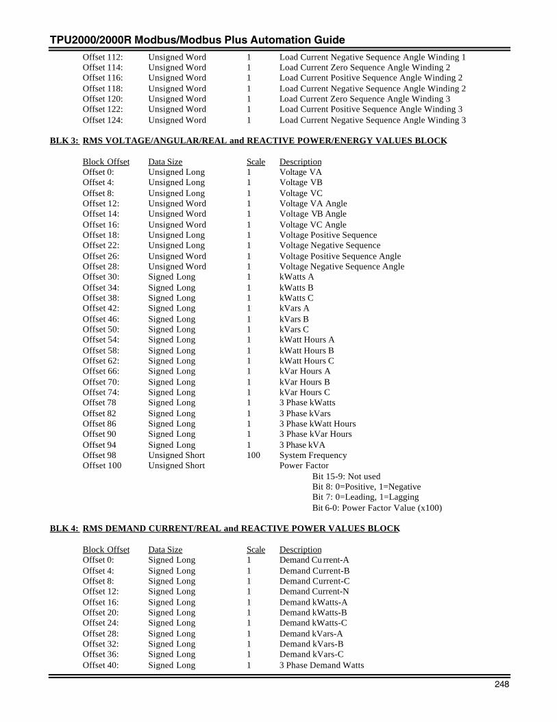
TPU2000/2000R Modbus/Modbus Plus Automation Guide
248
Offset 112: Unsigned Word 1 Load Current Negative Sequence Angle Winding 1Offset 114: Unsigned Word 1 Load Current Zero Sequence Angle Winding 2Offset 116: Unsigned Word 1 Load Current Positive Sequence Angle Winding 2Offset 118: Unsigned Word 1 Load Current Negative Sequence Angle Winding 2Offset 120: Unsigned Word 1 Load Current Zero Sequence Angle Winding 3Offset 122: Unsigned Word 1 Load Current Positive Sequence Angle Winding 3Offset 124: Unsigned Word 1 Load Current Negative Sequence Angle Winding 3
BLK 3: RMS VOLTAGE/ANGULAR/REAL and REACTIVE POWER/ENERGY VALUES BLOCK
Block Offset Data Size Scale DescriptionOffset 0: Unsigned Long 1 Voltage VAOffset 4: Unsigned Long 1 Voltage VB
Offset 8: Unsigned Long 1 Voltage VCOffset 12: Unsigned Word 1 Voltage VA AngleOffset 14: Unsigned Word 1 Voltage VB AngleOffset 16: Unsigned Word 1 Voltage VC AngleOffset 18: Unsigned Long 1 Voltage Positive SequenceOffset 22: Unsigned Long 1 Voltage Negative SequenceOffset 26: Unsigned Word 1 Voltage Positive Sequence AngleOffset 28: Unsigned Word 1 Voltage Negative Sequence AngleOffset 30: Signed Long 1 kWatts AOffset 34: Signed Long 1 kWatts BOffset 38: Signed Long 1 kWatts COffset 42: Signed Long 1 kVars AOffset 46: Signed Long 1 kVars BOffset 50: Signed Long 1 kVars COffset 54: Signed Long 1 kWatt Hours AOffset 58: Signed Long 1 kWatt Hours BOffset 62: Signed Long 1 kWatt Hours COffset 66: Signed Long 1 kVar Hours AOffset 70: Signed Long 1 kVar Hours BOffset 74: Signed Long 1 kVar Hours COffset 78 Signed Long 1 3 Phase kWattsOffset 82 Signed Long 1 3 Phase kVarsOffset 86 Signed Long 1 3 Phase kWatt HoursOffset 90 Signed Long 1 3 Phase kVar HoursOffset 94 Signed Long 1 3 Phase kVAOffset 98 Unsigned Short 100 System FrequencyOffset 100 Unsigned Short Power Factor
Bit 15-9: Not usedBit 8: 0=Positive, 1=NegativeBit 7: 0=Leading, 1=LaggingBit 6-0: Power Factor Value (x100)
BLK 4: RMS DEMAND CURRENT/REAL and REACTIVE POWER VALUES BLOCK
Block Offset Data Size Scale DescriptionOffset 0: Signed Long 1 Demand Cu rrent-AOffset 4: Signed Long 1 Demand Current-BOffset 8: Signed Long 1 Demand Current-COffset 12: Signed Long 1 Demand Current-NOffset 16: Signed Long 1 Demand kWatts-AOffset 20: Signed Long 1 Demand kWatts-BOffset 24: Signed Long 1 Demand kWatts-COffset 28: Signed Long 1 Demand kVars-AOffset 32: Signed Long 1 Demand kVars-BOffset 36: Signed Long 1 Demand kVars-COffset 40: Signed Long 1 3 Phase Demand Watts
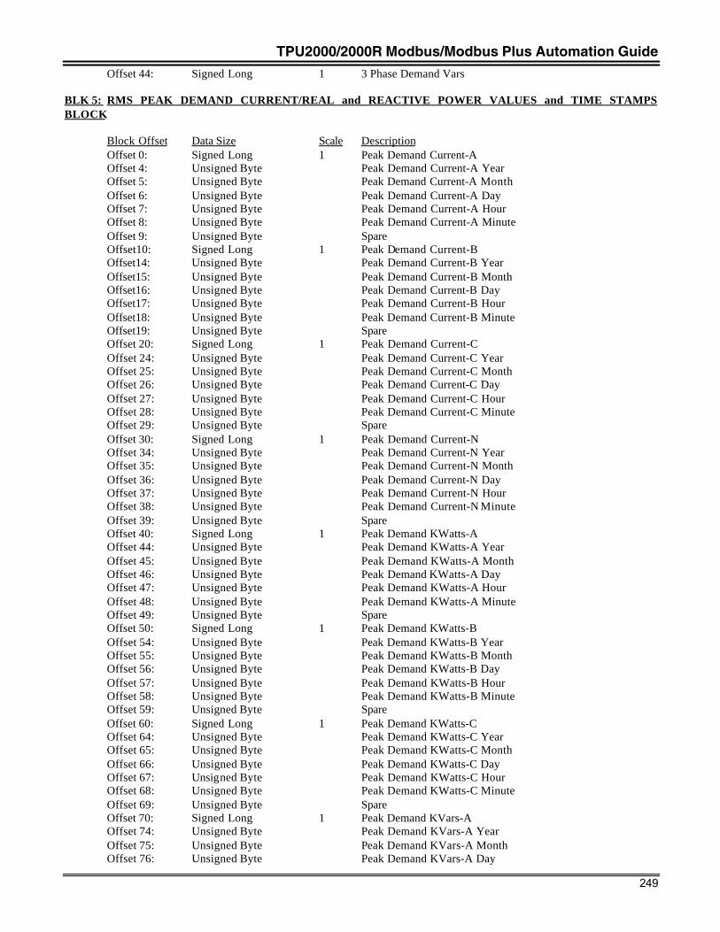
TPU2000/2000R Modbus/Modbus Plus Automation Guide
249
Offset 44: Signed Long 1 3 Phase Demand Vars
BLK 5: RMS PEAK DEMAND CURRENT/REAL and REACTIVE POWER VALUES and TIME STAMPSBLOCK
Block Offset Data Size Scale DescriptionOffset 0: Signed Long 1 Peak Demand Current-AOffset 4: Unsigned Byte Peak Demand Current-A YearOffset 5: Unsigned Byte Peak Demand Current-A MonthOffset 6: Unsigned Byte Peak Demand Current-A DayOffset 7: Unsigned Byte Peak Demand Current-A HourOffset 8: Unsigned Byte Peak Demand Current-A MinuteOffset 9: Unsigned Byte SpareOffset10: Signed Long 1 Peak Demand Current-BOffset14: Unsigned Byte Peak Demand Current-B YearOffset15: Unsigned Byte Peak Demand Current-B MonthOffset16: Unsigned Byte Peak Demand Current-B DayOffset17: Unsigned Byte Peak Demand Current-B HourOffset18: Unsigned Byte Peak Demand Current-B MinuteOffset19: Unsigned Byte SpareOffset 20: Signed Long 1 Peak Demand Current-COffset 24: Unsigned Byte Peak Demand Current-C YearOffset 25: Unsigned Byte Peak Demand Current-C MonthOffset 26: Unsigned Byte Peak Demand Current-C DayOffset 27: Unsigned Byte Peak Demand Current-C HourOffset 28: Unsigned Byte Peak Demand Current-C MinuteOffset 29: Unsigned Byte SpareOffset 30: Signed Long 1 Peak Demand Current-NOffset 34: Unsigned Byte Peak Demand Current-N YearOffset 35: Unsigned Byte Peak Demand Current-N MonthOffset 36: Unsigned Byte Peak Demand Current-N DayOffset 37: Unsigned Byte Peak Demand Current-N HourOffset 38: Unsigned Byte Peak Demand Current-N MinuteOffset 39: Unsigned Byte SpareOffset 40: Signed Long 1 Peak Demand KWatts-AOffset 44: Unsigned Byte Peak Demand KWatts-A YearOffset 45: Unsigned Byte Peak Demand KWatts-A MonthOffset 46: Unsigned Byte Peak Demand KWatts-A DayOffset 47: Unsigned Byte Peak Demand KWatts-A HourOffset 48: Unsigned Byte Peak Demand KWatts-A MinuteOffset 49: Unsigned Byte SpareOffset 50: Signed Long 1 Peak Demand KWatts-BOffset 54: Unsigned Byte Peak Demand KWatts-B YearOffset 55: Unsigned Byte Peak Demand KWatts-B MonthOffset 56: Unsigned Byte Peak Demand KWatts-B DayOffset 57: Unsigned Byte Peak Demand KWatts-B HourOffset 58: Unsigned Byte Peak Demand KWatts-B MinuteOffset 59: Unsigned Byte SpareOffset 60: Signed Long 1 Peak Demand KWatts-COffset 64: Unsigned Byte Peak Demand KWatts-C YearOffset 65: Unsigned Byte Peak Demand KWatts-C MonthOffset 66: Unsigned Byte Peak Demand KWatts-C DayOffset 67: Unsigned Byte Peak Demand KWatts-C HourOffset 68: Unsigned Byte Peak Demand KWatts-C MinuteOffset 69: Unsigned Byte SpareOffset 70: Signed Long 1 Peak Demand KVars-AOffset 74: Unsigned Byte Peak Demand KVars-A YearOffset 75: Unsigned Byte Peak Demand KVars-A MonthOffset 76: Unsigned Byte Peak Demand KVars-A Day
TPU2000/2000R Modbus/Modbus Plus Automation Guide
250
Offset 77: Unsigned Byte Peak Demand KVars-A HourOffset 78: Unsigned Byte Peak Demand KVars-A MinuteOffset 79: Unsigned Byte SpareOffset 80: Signed Long 1 Peak Demand KVars-BOffset 84: Unsigned Byte Peak Demand KVars-B YearOffset 85: Unsigned Byte Peak Demand KVars-B MonthOffset 86: Unsigned Byte Peak Demand KVars-B DayOffset 87: Unsigned Byte Peak Demand KVars-B HourOffset 88: Unsigned Byte Peak Demand KVars-B MinuteOffset 89: Unsigned Byte SpareOffset 90: Signed Long 1 Peak Demand KVars-COffset 94: Unsigned Byte Peak Demand KVars-C YearOffset 95: Unsigned Byte Peak Demand KVars-C MonthOffset 96: Unsigned Byte Peak Demand KVars-C DayOffset 97: Unsigned Byte Peak Demand KVars-C HourOffset 98: Unsigned Byte Peak Demand KVars-C MinuteOffset 99: Unsigned Byte SpareOffset 100: Signed Long 1 3 Phase Peak Demand KWattsOffset 104: Unsigned Byte 3 Phase Peak Demand KWatts YearOffset 105: Unsigned Byte 3 Phase Peak Demand KWatts MonthOffset 106: Unsigned Byte 3 Phase Peak Demand KWatts DayOffset 107: Unsigned Byte 3 Phase Peak Demand KWatts HourOffset 108: Unsigned Byte 3 Phase Peak Demand KWatts MinuteOffset 109: Unsigned Byte SpareOffset 110: Signed Long 1 3 Phase Peak Demand KVarsOffset 114: Unsigned Byte 3 Phase Peak Demand KVars YearOffset 115: Unsigned Byte 3 Phase Peak Demand KVars MonthOffset 116: Unsigned Byte 3 Phase Peak Demand KVars DayOffset 117: Unsigned Byte 3 Phase Peak Demand KVars HourOffset 118: Unsigned Byte 3 Phase Peak Demand KVars MinuteOffset 119: Unsigned Byte Spare
BLK 6: RMS MINIMUM DEMAND CURRENT/REAL and REACTIVE POWER VALUES and TIME STAMPSBLOCK
Block Offset Data Size Scale DescriptionOffset 0: Signed Long 1 Minimum Demand Current-AOffset 4: Unsigned Byte Minimum Demand Current-A YearOffset 5: Unsigned Byte Minimum Demand Current-A MonthOffset 6: Unsigned Byte Minimum Demand Current-A DayOffset 7: Unsigned Byte Minimum Demand Current-A HourOffset 8: Unsigned Byte Minimum Demand Current-A MinuteOffset 9: Unsigned Byte SpareOffset10: Signed Long 1 Minimum Demand Current-BOffset14: Unsigned Byte Minimum Demand Current-B YearOffset15: Unsigned Byte Minimum Demand Current-B MonthOffset16: Unsigned Byte Minimum Demand Current-B DayOffset17: Unsigned Byte Minimum De mand Current-B HourOffset18: Unsigned Byte Minimum Demand Current-B MinuteOffset19: Unsigned Byte SpareOffset 20: Signed Long 1 Minimum Demand Current-COffset 24: Unsigned Byte Minimum Demand Current-C YearOffset 25: Unsigned Byte Minimum Demand Current-C MonthOffset 26: Unsigned Byte Minimum Demand Current-C DayOffset 27: Unsigned Byte Minimum Demand Current-C HourOffset 28: Unsigned Byte Minimum Demand Current-C MinuteOffset 29: Unsigned Byte Spare Offset 30: Signed Long 1 Minimum Demand Current-NOffset 34: Unsigned Byte Minimum Demand Current-N Year
TPU2000/2000R Modbus/Modbus Plus Automation Guide
251
Offset 35: Unsigned Byte Minimum Demand Current-N MonthOffset 36: Unsigned Byte Minimum Demand Current-N DayOffset 37: Unsigned Byte Minimum Demand Current-N HourOffset 38: Unsigned Byte Minimum Demand Current-N MinuteOffset 39: Unsigned Byte SpareOffset 40: Signed Long 1 Minimum Demand KWatts-AOffset 44: Unsigned Byte Minimum Demand KWatts-A YearOffset 45: Unsigned Byte Minimum Demand KWatts-A MonthOffset 46: Unsigned Byte Minimum Demand KWatts-A DayOffset 47: Unsigned Byte Minimum Demand KWatts-A HourOffset 48: Unsigned Byte Minimum Demand KWatts-A MinuteOffset 49: Unsigned Byte SpareOffset 50: Signed Long 1 Minimum Demand KWatts-BOffset 54: Unsigned Byte Minimum Demand KWatts-B YearOffset 55: Unsigned Byte Minimum Demand KWatts-B MonthOffset 56: Unsigned Byte Minimum Demand KWatts-B DayOffset 57: Unsigned Byte Minimum Demand KWatts-B HourOffset 58: Unsigned Byte Minimum Demand KWatts-B MinuteOffset 59: Unsigned Byte SpareOffset 60: Signed Long 1 Minimum Demand KWatts-COffset 64: Unsigned Byte Minimum Demand KWatts-C YearOffset 65: Unsigned Byte Minimum Demand KWatts-C MonthOffset 66: Unsigned Byte Minimum Demand KWatts-C DayOffset 67: Unsigned Byte Minimum Demand KWatts-C HourOffset 68: Unsigned Byte Minimum Demand KWatts-C MinuteOffset 69: Unsigned Byte SpareOffset 70: Signed Long 1 Minimum Demand KVars-AOffset 74: Unsigned Byte Minimum Demand KVars-A YearOffset 75: Unsigned Byte Minimum Demand KVars-A MonthOffset 76: Unsigned Byte Minimum Demand KVars-A DayOffset 77: Unsigned Byte Minimum Demand KVars-A HourOffset 78: Unsigned Byte Minimum Demand KVars-A MinuteOffset 79: Unsigned Byte SpareOffset 80: Signed Long 1 Minimum Demand KVars-BOffset 84: Unsigned Byte Minimum Demand KVars-B YearOffset 85: Unsigned Byte Minimum Demand KVars-B MonthOffset 86: Unsigned Byte Minimum Demand KVars-B DayOffset 87: Unsigned Byte Minimum Demand KVars-B HourOffset 88: Unsigned Byte Minimum Demand KVars-B MinuteOffset 89: Unsigned Byte Spare Offset 90: Signed Long 1 Minimum Demand KVars-COffset 94: Unsigned Byte Minimum Demand KVars-C YearOffset 95: Unsigned Byte Minimum Demand KVars-C MonthOffset 96: Unsigned Byte Minimum Demand KVars-C DayOffset 97: Unsigned Byte Minimum Demand KVars-C HourOffset 98: Unsigned Byte Minimum Demand KVars-C MinuteOffset 99: Unsigned Byte SpareOffset 100: Signed Long 1 3 Phase Minimum Demand KWattsOffset 104: Unsigned Byte 3 Phase Minimum Demand KWatts YearOffset 105: Unsigned Byte 3 Phase Minimum Demand KWatts MonthOffset 106: Unsigned Byte 3 Phase Minimum Demand KWatts DayOffset 107: Unsigned Byte 3 Phase Minimum Demand KWatts HourOffset 108: Unsigned Byte 3 Phase Minimum Demand KWatts MinuteOffset 109: Unsigned Byte SpareOffset 110: Signed Long 1 3 Phase Minimum Demand KVarsOffset 114: Unsigned Byte 3 Phase Minimum Demand KVars YearOffset 115: Unsigned Byte 3 Phase Minimum Demand KVars MonthOffset 116: Unsigned Byte 3 Phase Minimum Demand KVars DayOffset 117: Unsigned Byte 3 Phase Minimum Demand KVars Hour
TPU2000/2000R Modbus/Modbus Plus Automation Guide
252
Offset 118: Unsigned Byte 3 Phase Minimum Demand KVars MinuteOffset 119: Unsigned Byte Spare
BLK 7: COUNTERS BLOCK
Block Offset Data Size Scale DescriptionOffset 0: Unsigned Short 1 Unreported Differential Fault Record CounterOffset 2: Unsigned Short 1 Unreported Through Fault Record CounterOffset 4: Unsigned Short 1 Unreported Harmonic Restraint Record CounterOffset 6: Unsigned Short 1 Unreported Operation Record CounterOffset 8: Unsigned Short 1 Through Fault CounterOffset 10: Unsigned Long 1 Through Fault Summation kAmps-A CounterOffset 14: Unsigned Long 1 Through Fault Summation kAmps-B CounterOffset 18: Unsigned Long 1 Through Fault Summation kAmps-C CounterOffset 22: Unsigned Long 1 Through Fault Summation Cycles CounterOffset 26: Unsigned Short 1 Overcurrent Trip CounterOffset 28: Unsigned Short 1 Differential Trip Counter
BLK 8: PHYSICAL and LOGICAL INPUT/OUTPUT BLOCK
Block Offset Data Size DescriptionOffset 0: Unsigned Long Logical Output 0-31
Bit 31: DIFF Bit 15: 51G-2Bit 30: ALARM Bit 14: 50N-1Bit 29: 87T Bit 13: 150N-1Bit 28: 87H Bit 12: 50G-2Bit 27: 2HROA Bit 11: 150G-2Bit 26: 5HROA Bit 10: 46-1Bit 25: AHROA Bit 9: 46-2Bit 24: TCFA Bit 8: 87T-DBit 23: TFA Bit 7: 87H-DBit 22: 51P-1 Bit 6: 51P-1DBit 21: 51P-2 Bit 5: 51P-2DBit 20: 50P-1 Bit 4: 51N-1DBit 19: 150P-1 Bit 3: 51G-2DBit 18: 50P-2 Bit 2: 50P-1DBit 17: 150P-2 Bit 1: 50P-2DBit 16: 51N-1 Bit 0: 50N-1D
Offset 4: Unsigned Long Logical Output 32-63Bit 31: 50G-2D Bit 15: DTCBit 30: 150P-1D Bit 14: OCTCBit 29: 150P-2D Bit 13: PDABit 28: 150N-1D Bit 12: NDABit 27: 150G-2D Bit 11: PRIMBit 26: 46-1D Bit 10: ALT1Bit 25: 46-2D Bit 9: ALT2Bit 24: PATA Bit 8: STCABit 23: PBTA Bit 7: 87T*Bit 22: PCTA Bit 6: 87H*Bit 21: PUA Bit 5: 2HROA*Bit 20: 63 Bit 4: 5HROA*Bit 19: THRUFA Bit 3: AHROA*Bit 18: TFCA Bit 2: 51P-1*Bit 17: TFKA Bit 1: 51P-2*Bit 16: TFSCA Bit 0: 50P-1*
Offset 8: Unsigned Long Logical Output 64-95Bit 31: 150P-1* Bit 15: ULO5Bit 30: 50P-2* Bit 14: ULO6Bit 29: 150P-2* Bit 13: ULO7
TPU2000/2000R Modbus/Modbus Plus Automation Guide
253
Bit 28: 51N-1* Bit 12: ULO8Bit 27: 51G-2* Bit 11: ULO9Bit 26: 50N-1* Bit 10: LOADABit 25: 150N-1* Bit 9: OCA-1Bit 24: 50G-2* Bit 8: OCA-2Bit 23: 150G-2* Bit 7: HLDA-1Bit 22: 46-1* Bit 6: LLDA-1Bit 21: 46-2* Bit 5: HLDA-2Bit 20: 63* Bit 4: LLDA-1Bit 19: ULO1 Bit 3: HPFABit 18: ULO2 Bit 2: LPFABit 17: ULO3 Bit 1: VarDABit 16: ULO4 Bit 0: PVarA
Offset 12: Unsigned Long Logical Output 96-127Bit 31: NVarA Bit 15:Bit 30: PWatt1 Bit 14:Bit 29: PWatt2 Bit 13:Bit 28: Bit 12:Bit 27: Bit 11:Bit 26: Bit 10:Bit 25: Bit 9:Bit 24: Bit 8:Bit 23: Bit 7:Bit 22: Bit 6:Bit 21: Bit 5:Bit 20: Bit 4:Bit 19: Bit 3:Bit 18: Bit 2:Bit 17: Bit 1:Bit 16: Bit 0:
Offset 16: Unsigned Long Logical Input 0-31Bit 31: 87T Bit 15: ALT1Bit 30: 87H Bit 14: ALT2Bit 29: 51P-1 Bit 13: ECI1Bit 28: 51P-2 Bit 12: ECI2Bit 27: 51N-1 Bit 11: WCIBit 26: 51G-2 Bit 10: TRIPBit 25: 50P-1 Bit 9: SPRBit 24: 50P-2 Bit 8: TCMBit 23: 50N-1 Bit 7: ULI1Bit 22: 50G-2 Bit 6: ULI2Bit 21: 150P-1 Bit 5: ULI3Bit 20: 150P-2 Bit 4: ULI4Bit 19: 150N-1 Bit 3: ULI5Bit 18: 150G-2 Bit 2: ULI6Bit 17: 46-1 Bit 1: ULI7Bit 16: 46-2 Bit 0: ULI8
Offset 20: Unsigned Long Logical Input 32-63Bit 31: ULI9 Bit 15:Bit 30: CRI Bit 14:Bit 29: Bit 13:Bit 28: Bit 12:Bit 27: Bit 11:Bit 26: Bit 10:Bit 25: Bit 9:Bit 24: Bit 8:Bit 23: Bit 7:Bit 22: Bit 6:Bit 21: Bit 5:
TPU2000/2000R Modbus/Modbus Plus Automation Guide
254
Bit 20: Bit 4:Bit 19: Bit 3:Bit 18: Bit 2:Bit 17: Bit 1:Bit 16: Bit 0:
Offset 24: Unsigned Long Logical Input 64-95 (Reserved)Offset 28: Unsigned Long Logical Input 96-127 (Reserved)Offset 32: Unsigned Short Physical Output
Bit 15: Spare Bit 7: OUT7Bit 14: Spare Bit 6: OUT6Bit 13: Spare Bit 5: OUT5Bit 12: Spare Bit 4: OUT4Bit 11: Spare Bit 3: OUT3Bit 10: Spare Bit 2: OUT2Bit 9: Spare Bit 1: OUT1Bit 8: Spare Bit 0: TRIP
Offset 34: Unsigned Short Physical InputBit 15: Spare Bit 7: IN8Bit 14: Spare Bit 6: IN7Bit 13: Spare Bit 5: IN6Bit 12: Spare Bit 4: IN5Bit 11: Spare Bit 3: IN4Bit 10: Spare Bit 2: IN3Bit 9: Spare Bit 1: IN2Bit 8: IN9 Bit 0: IN1
3 Transmit Buffer "N" Commands ( 3 3 n )
N Definition 0 Reserved for repeat 3 3 n 1 Communications Settings
3.1 Transmit Communications Settings ( 3 3 1 )
Low byte consists of bits 0 through 7.High byte consists of bits 8 through 15.
Port configuration bytebit0-3 = port baud rate where 0 = 300, 1 = 1200, 2 = 2400, 3 = 4800, 4 = 9600, 5 = 19200,6 = 38400bit 4-5 = parity (0=None,1=Odd,2=Even)bit 6 = number of data bits (0=seven,1=eight)bit 7 = number of stop bits (0=one,1=two)
Valid Frame Combinations (EVEN 7 1, ODD 7 1, NONE 8 1, EVEN 8 1, ODD 8 1, NONE 8 2, NONE 7 2)
Msg byte Definition1/1 Relay Status (see command 3 4 1, msg 1/1)1/2 Command + Subcommand = 0x311/3 Total Number of Messages = 92/1 Unit Address high byte2/2 Unit Address low byte2/3 Front Panel RS232 configuration byte3/1 Rear Panel RS232 or INCOM configuration byte3/2 Rear Panel RS485 configuration byte3/3 Rear Panel IRIG byte 0=Disabled, 1=Enabled4/1 Spare
4/2 Spare4/3 Aux Port Parameter 1 byte (0-255)5/1 Aux Port Parameter 2 byte (0-255)
TPU2000/2000R Modbus/Modbus Plus Automation Guide
255
5/2 Aux Port Parameter 3 byte (0-255)5/3 Aux Port Parameter 4 byte (0-255)6/1 Aux Port Parameter 5 byte (0-255)6/2 Aux Port Parameter 6 byte (0-255)6/3 Aux Port Parameter 7 byte (0-255)7/1 Aux Port Parameter 8 byte (0-255)7/2 Aux Port Parameter 9 byte (0-255)7/3 Aux Port Parameter 10 byte (0-255)8/1 Aux Port Parameter Mode byte8/2 Spare
8/3 Spare9/1 Spare9/2 Checksum high byte9/3 Checksum low byte
4 Transmit Buffer "N" Commands ( 3 4 n )
N Definition 0 Reserved for repeat 3 4 n 1 Programmable Input Select and Index Tables 2 Programmable Input Negated AND Table 3 Programmable Input AND/OR Table 4 Programmable Input User Defined Input Names 5 Programmable Output Select Table 6 Programmable Output AND/OR Table 7 Programmable Output User Defined Output Strings 8 Primary Relay Settings 9 Alternate 1 Relay Settings10 Alternate 2 Relay Settings11 Configuration Settings12 Counter Settings13 Alarm Settings14 Real Time Clock15 Output Delays
4.1 Transmit Programmable Input Select and Index ( 3 4 1 )
Bit = 0, Physical Input is selected.Bit = 1, Physical Input is not selected.Low byte consists of bits 0 through 7.High byte consists of bits 8 through 15.Index byte is the offset into the TPU's logical input structure.
Offset Definitions 00 87T Restrained Differential Trip 01 87H High Set Inst Differential Trip 02 51P-1 Wdg1 Phase Time OC Trip 03 51P-2 Wdg2 Phase Time OC Trip 04 51N-1 Wdg1 Neutral Time OC Trip 05 51G-2 Wdg2 Ground Time OC Trip 06 50P-1 1st Wdg1 Phase Inst OC Trip 07 50P-2 1st Wdg2 Phase Inst OC Trip 08 50N-1 1st Wdg1 Neutral Inst OC Trip 09 50G-2 1st Wdg2 Ground Inst OC Trip 10 150P-1 2nd Wdg1 Phase Inst OC Trip 11 150P-2 2nd Wdg2 Phase Inst OC Trip 12 150N-1 2nd Wdg1 Neutral Inst OC Trip 13 150G-2 2nd Wdg2 Ground Inst OC Trip 14 46-1 Wdg1 Neg Seq Time OC Trip
TPU2000/2000R Modbus/Modbus Plus Automation Guide
256
15 46-2 Wdg2 Neg Seq Time OC Trip 16 ALT1 Enables Alt 1 Settings 17 ALT2 Enables Alt 2 Settings 18 ECI1 Event-1 Capture Initiated 19 ECI2 Event-2 Capture Initiated 20 WCI Waveform Capture Initiated 21 Trip Initiates Diff Trip Output 22 SPR Sudden Pressure Input 23 TCM Trip Coil Monitoring 24 ULI1 User Logical Input 1 25 ULI2 User Logical Input 2 26 ULI3 User Logical Input 3 27 ULI4 User Logical Input 4 28 ULI5 User Logical Input 5 29 ULI6 User Logical Input 6 30 ULI7 User Logical Input 7 31 ULI8 User Logical Input 8 32 ULI9 User Logical Input 9 33 CRI Clears Through Fault and OC Counters
Example : if message 2/1 = hex 242/2 = hex 11
2/3 = hex 4I/O word is 00100100 00010001 hex 2411
Note the Physical Inputs are translated using the physical input table below: In the example IN3, IN10, IN8 and IN5 areselected for GND.
The AND/OR selection and enable disable mapping is selected with commands 3 11 3 and 3 11 2
Bit Physical Input--- --------------0 IN6
1 IN7 2 IN8 3 IN2
4 IN9 5 IN3
6 IN47 IN58 IN1
9 Reserved10 Reserved11 Reserved12 Reserved
13 Reserved 14 Reserved
15 Reserved
Msg byte Definition 1/1 Relay Status
Bit 0 : SelfTest Status Bit 1 : Contact Input Status changed Bit 2 : Local Settings Change Bit 3 : Remote Edit Disabled. Bit 4 : Alternate Settings Group 1 enabled. Bit 5 : Alternate Setting Group 2 enabled. Bit 6 : Fault Record Logged. Bit 7 : Power was Cycled
TPU2000/2000R Modbus/Modbus Plus Automation Guide
257
1/2 Command + Subcommand = 0x41 1/3 Total Number of Messages = 34 2/1 INPUT1 high byte 2/2 INPUT1 low byte 2/3 INPUT1 index byte 3/1 INPUT2 high byte 3/2 INPUT2 low byte 3/3 INPUT2 index byte 4/1 INPUT3 high byte 4/2 INPUT3 low byte 4/3 INPUT3 index byte 5/1 INPUT4 high byte 5/2 INPUT4 low byte Bit Physical Input 5/3 INPUT4 index byte --- -------------- 6/1 INPUT5 high byte 0 IN6 6/2 INPUT5 low byte 1 IN7 6/3 INPUT5 index byte 2 IN8 7/1 INPUT6 high byte 3 IN2 7/2 INPUT6 low byte 4 IN9 7/3 INPUT6 index byte 5 IN3 8/1 INPUT7 high byte 6 IN4 8/2 INPUT7 low byte 7 IN5 8/3 INPUT7 index byte 8 IN1 9/1 INPUT8 high byte 9 Reserved 9/2 INPUT8 low byte 10 Reserved 9/3 INPUT8 index byte 11 Reserved 10/1 INPUT9 high byte 12 Reserved 10/2 INPUT9 low byte 13 Reserved 10/3 INPUT9 index byte 14 Reserved 11/1 INPUT10 high byte 15 Reserved 11/2 INPUT10 low byte 11/3 INPUT10 index byte 12/1 INPUT11 high byte 12/2 INPUT11 low byte 12/3 INPUT11 index byte 13/1 INPUT12 high byte 13/2 INPUT12 low byte 13/3 INPUT12 index byte 14/1 INPUT13 high byte 14/2 INPUT13 low byte 14/3 INPUT13 index byte 15/1 INPUT14 high byte 15/2 INPUT14 low byte 15/3 INPUT14 index byte 16/1 INPUT15 high byte 16/2 INPUT15 low byte 16/3 INPUT15 index byte 17/1 INPUT16 high byte 17/2 INPUT16 low byte 17/3 INPUT16 index byte 18/1 INPUT17 high byte 18/2 INPUT17 low byte 18/3 INPUT17 index byte 19/1 INPUT18 high byte 19/2 INPUT18 low byte 19/3 INPUT18 index byte 20/1 INPUT19 high byte 20/2 INPUT19 low byte 20/3 INPUT19 index byte
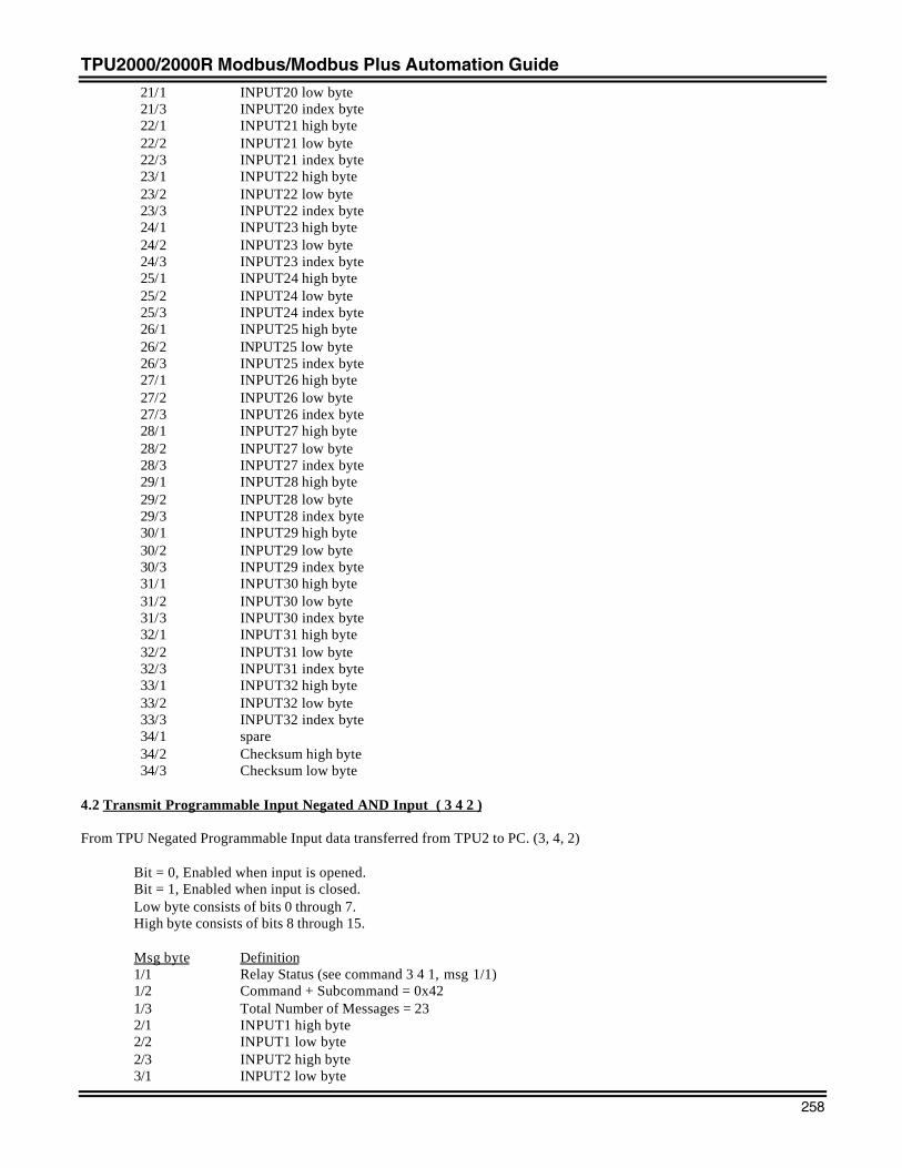
TPU2000/2000R Modbus/Modbus Plus Automation Guide
258
21/1 INPUT20 low byte 21/3 INPUT20 index byte 22/1 INPUT21 high byte 22/2 INPUT21 low byte 22/3 INPUT21 index byte 23/1 INPUT22 high byte 23/2 INPUT22 low byte 23/3 INPUT22 index byte 24/1 INPUT23 high byte 24/2 INPUT23 low byte 24/3 INPUT23 index byte 25/1 INPUT24 high byte 25/2 INPUT24 low byte 25/3 INPUT24 index byte 26/1 INPUT25 high byte 26/2 INPUT25 low byte 26/3 INPUT25 index byte 27/1 INPUT26 high byte 27/2 INPUT26 low byte 27/3 INPUT26 index byte 28/1 INPUT27 high byte 28/2 INPUT27 low byte 28/3 INPUT27 index byte 29/1 INPUT28 high byte 29/2 INPUT28 low byte 29/3 INPUT28 index byte 30/1 INPUT29 high byte 30/2 INPUT29 low byte 30/3 INPUT29 index byte 31/1 INPUT30 high byte 31/2 INPUT30 low byte 31/3 INPUT30 index byte 32/1 INPUT31 high byte 32/2 INPUT31 low byte 32/3 INPUT31 index byte 33/1 INPUT32 high byte 33/2 INPUT32 low byte 33/3 INPUT32 index byte 34/1 spare 34/2 Checksum high byte 34/3 Checksum low byte
4.2 Transmit Programmable Input Negated AND Input ( 3 4 2 )
From TPU Negated Programmable Input data transferred from TPU2 to PC. (3, 4, 2)
Bit = 0, Enabled when input is opened.Bit = 1, Enabled when input is closed.Low byte consists of bits 0 through 7.High byte consists of bits 8 through 15.
Msg byte Definition1/1 Relay Status (see command 3 4 1, msg 1/1)1/2 Command + Subcommand = 0x421/3 Total Number of Messages = 232/1 INPUT1 high byte2/2 INPUT1 low byte2/3 INPUT2 high byte3/1 INPUT2 low byte
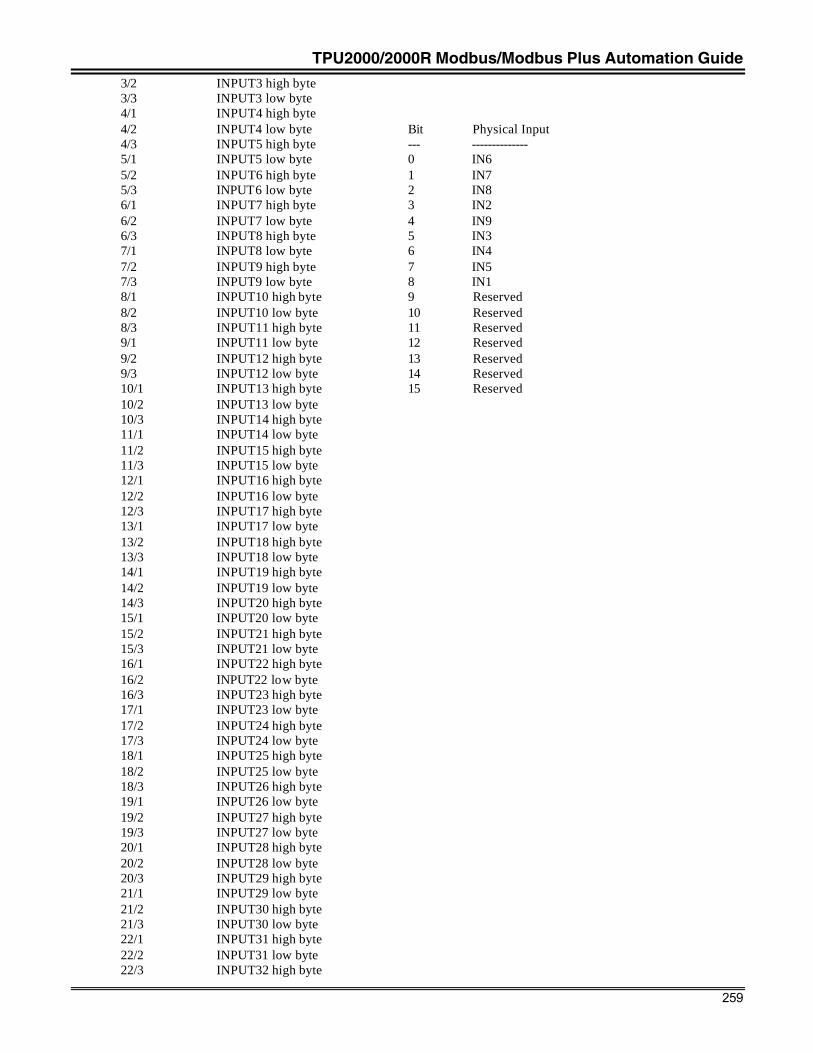
TPU2000/2000R Modbus/Modbus Plus Automation Guide
259
3/2 INPUT3 high byte3/3 INPUT3 low byte4/1 INPUT4 high byte4/2 INPUT4 low byte Bit Physical Input4/3 INPUT5 high byte --- --------------5/1 INPUT5 low byte 0 IN65/2 INPUT6 high byte 1 IN75/3 INPUT6 low byte 2 IN86/1 INPUT7 high byte 3 IN26/2 INPUT7 low byte 4 IN96/3 INPUT8 high byte 5 IN37/1 INPUT8 low byte 6 IN47/2 INPUT9 high byte 7 IN57/3 INPUT9 low byte 8 IN18/1 INPUT10 high byte 9 Reserved8/2 INPUT10 low byte 10 Reserved8/3 INPUT11 high byte 11 Reserved9/1 INPUT11 low byte 12 Reserved9/2 INPUT12 high byte 13 Reserved9/3 INPUT12 low byte 14 Reserved10/1 INPUT13 high byte 15 Reserved10/2 INPUT13 low byte10/3 INPUT14 high byte11/1 INPUT14 low byte11/2 INPUT15 high byte11/3 INPUT15 low byte12/1 INPUT16 high byte12/2 INPUT16 low byte12/3 INPUT17 high byte13/1 INPUT17 low byte13/2 INPUT18 high byte13/3 INPUT18 low byte14/1 INPUT19 high byte14/2 INPUT19 low byte14/3 INPUT20 high byte15/1 INPUT20 low byte15/2 INPUT21 high byte15/3 INPUT21 low byte16/1 INPUT22 high byte16/2 INPUT22 low byte16/3 INPUT23 high byte17/1 INPUT23 low byte17/2 INPUT24 high byte17/3 INPUT24 low byte18/1 INPUT25 high byte18/2 INPUT25 low byte18/3 INPUT26 high byte19/1 INPUT26 low byte19/2 INPUT27 high byte19/3 INPUT27 low byte20/1 INPUT28 high byte20/2 INPUT28 low byte20/3 INPUT29 high byte21/1 INPUT29 low byte21/2 INPUT30 high byte21/3 INPUT30 low byte22/1 INPUT31 high byte22/2 INPUT31 low byte22/3 INPUT32 high byte
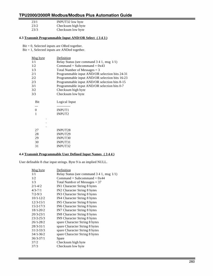
TPU2000/2000R Modbus/Modbus Plus Automation Guide
260
23/1 INPUT32 low byte23/2 Checksum high byte23/3 Checksum low byte
4.3 Transmit Programmable Input AND/OR Select ( 3 4 3 )
Bit = 0, Selected inputs are ORed together. Bit = 1, Selected inputs are ANDed together.
Msg byte Definition1/1 Relay Status (see command 3 4 1, msg 1/1)1/2 Command + Subcommand = 0x431/3 Total Number of Messages = 32/1 Programmable input AND/OR selection bits 24-312/2 Programmable input AND/OR selection bits 16-232/3 Programmable input AND/OR selection bits 8-153/1 Programmable input AND/OR selection bits 0-73/2 Checksum high byte3/3 Checksum low byte
Bit Logical Input --- ------------- 0 INPUT1 1 INPUT2 . . . 27 INPUT28 28 INPUT29 29 INPUT30 30 INPUT31 31 INPUT32
4.4 Transmit Programmable User Defined Input Names ( 3 4 4 )
User definable 8 char input strings. Byte 9 is an implied NULL.
Msg byte Definition1/1 Relay Status (see command 3 4 1, msg 1/1)1/2 Command + Subcommand = 0x441/3 Total Numb er of Messages = 372/1-4/2 IN1 Character String 8 bytes4/3-7/1 IN2 Character String 8 bytes7/2-9/3 IN3 Character String 8 bytes10/1-12/2 IN4 Character String 8 bytes12/3-15/1 IN5 Character String 8 bytes15/2-17/3 IN6 Character String 8 bytes18/1-20/2 IN7 Character String 8 bytes20/3-23/1 IN8 Character String 8 bytes23/2-25/3 IN9 Character String 8 bytes26/1-28/2 spare Character String 8 bytes28/3-31/1 spare Character String 8 bytes31/2-33/3 spare Character String 8 bytes34/1-36/2 spare Character String 8 bytes36/3-37/1 Spare37/2 Checksum high byte37/3 Checksum low byte
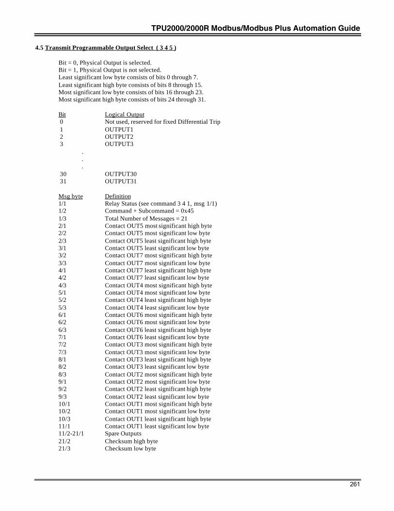
TPU2000/2000R Modbus/Modbus Plus Automation Guide
261
4.5 Transmit Programmable Output Select ( 3 4 5 )
Bit = 0, Physical Output is selected.Bit = 1, Physical Output is not selected.Least significant low byte consists of bits 0 through 7.Least significant high byte consists of bits 8 through 15.Most significant low byte consists of bits 16 through 23.Most significant high byte consists of bits 24 through 31.
Bit Logical Output 0 Not used, reserved for fixed Differential Trip 1 OUTPUT1 2 OUTPUT2 3 OUTPUT3
. . . 30 OUTPUT30 31 OUTPUT31
Msg byte Definition1/1 Relay Status (see command 3 4 1, msg 1/1)1/2 Command + Subcommand = 0x451/3 Total Number of Messages = 212/1 Contact OUT5 most significant high byte2/2 Contact OUT5 most significant low byte2/3 Contact OUT5 least significant high byte3/1 Contact OUT5 least significant low byte3/2 Contact OUT7 most significant high byte3/3 Contact OUT7 most significant low byte4/1 Contact OUT7 least significant high byte4/2 Contact OUT7 least significant low byte4/3 Contact OUT4 most significant high byte5/1 Contact OUT4 most significant low byte5/2 Contact OUT4 least significant high byte5/3 Contact OUT4 least significant low byte6/1 Contact OUT6 most significant high byte6/2 Contact OUT6 most significant low byte6/3 Contact OUT6 least significant high byte7/1 Contact OUT6 least significant low byte7/2 Contact OUT3 most significant high byte7/3 Contact OUT3 most significant low byte8/1 Contact OUT3 least significant high byte8/2 Contact OUT3 least significant low byte8/3 Contact OUT2 most significant high byte9/1 Contact OUT2 most significant low byte9/2 Contact OUT2 least significant high byte9/3 Contact OUT2 least significant low byte10/1 Contact OUT1 most significant high byte10/2 Contact OUT1 most significant low byte10/3 Contact OUT1 least significant high byte11/1 Contact OUT1 least significant low byte11/2-21/1 Spare Outputs21/2 Checksum high byte21/3 Checksum low byte
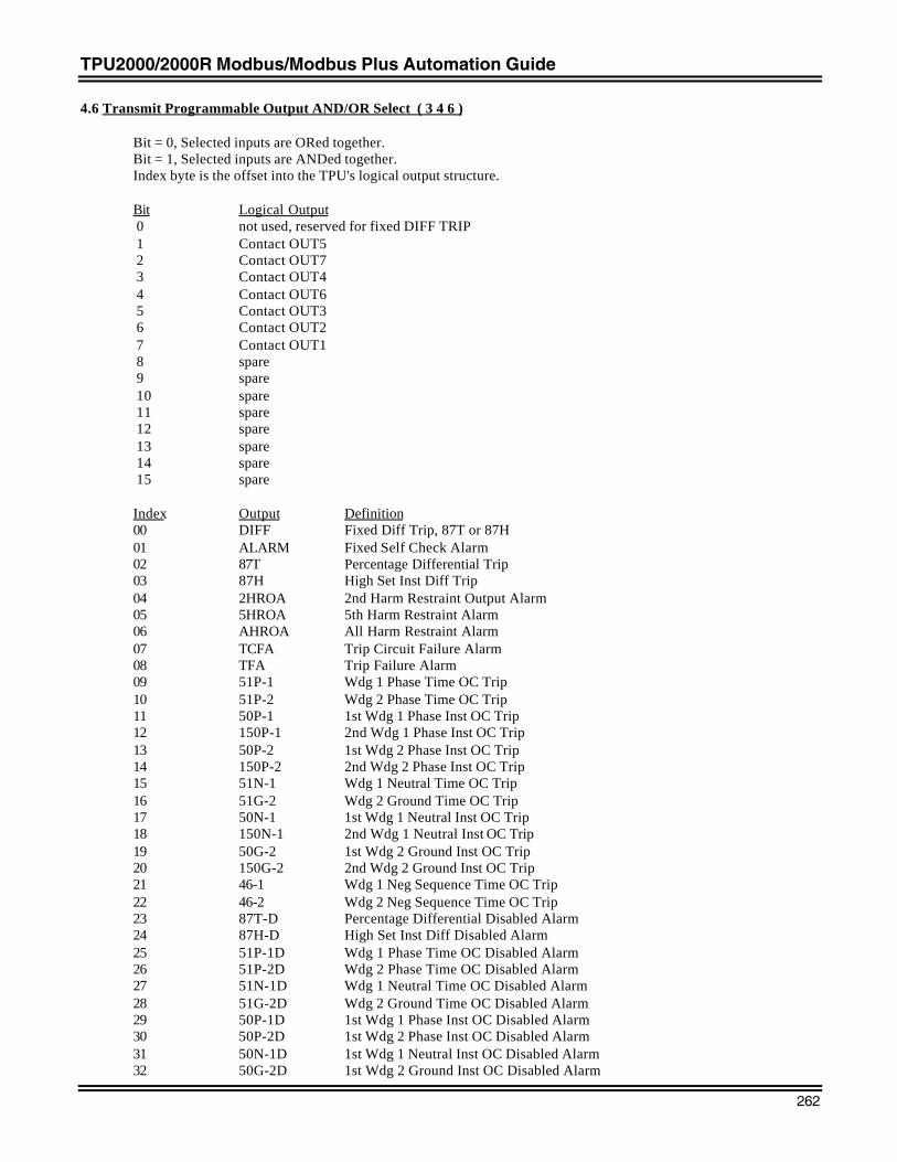
TPU2000/2000R Modbus/Modbus Plus Automation Guide
262
4.6 Transmit Programmable Output AND/OR Select ( 3 4 6 )
Bit = 0, Selected inputs are ORed together.Bit = 1, Selected inputs are ANDed together.Index byte is the offset into the TPU's logical output structure.
Bit Logical Output 0 not used, reserved for fixed DIFF TRIP 1 Contact OUT5 2 Contact OUT7 3 Contact OUT4 4 Contact OUT6 5 Contact OUT3 6 Contact OUT2 7 Contact OUT1 8 spare 9 spare 10 spare 11 spare 12 spare 13 spare 14 spare 15 spare
Index Output Definition00 DIFF Fixed Diff Trip, 87T or 87H01 ALARM Fixed Self Check Alarm02 87T Percentage Differential Trip03 87H High Set Inst Diff Trip04 2HROA 2nd Harm Restraint Output Alarm05 5HROA 5th Harm Restraint Alarm06 AHROA All Harm Restraint Alarm07 TCFA Trip Circuit Failure Alarm08 TFA Trip Failure Alarm09 51P-1 Wdg 1 Phase Time OC Trip10 51P-2 Wdg 2 Phase Time OC Trip11 50P-1 1st Wdg 1 Phase Inst OC Trip12 150P-1 2nd Wdg 1 Phase Inst OC Trip13 50P-2 1st Wdg 2 Phase Inst OC Trip14 150P-2 2nd Wdg 2 Phase Inst OC Trip15 51N-1 Wdg 1 Neutral Time OC Trip16 51G-2 Wdg 2 Ground Time OC Trip17 50N-1 1st Wdg 1 Neutral Inst OC Trip18 150N-1 2nd Wdg 1 Neutral Inst OC Trip19 50G-2 1st Wdg 2 Ground Inst OC Trip20 150G-2 2nd Wdg 2 Ground Inst OC Trip21 46-1 Wdg 1 Neg Sequence Time OC Trip22 46-2 Wdg 2 Neg Sequence Time OC Trip23 87T-D Percentage Differential Disabled Alarm24 87H-D High Set Inst Diff Disabled Alarm25 51P-1D Wdg 1 Phase Time OC Disabled Alarm26 51P-2D Wdg 2 Phase Time OC Disabled Alarm27 51N-1D Wdg 1 Neutral Time OC Disabled Alarm28 51G-2D Wdg 2 Ground Time OC Disabled Alarm29 50P-1D 1st Wdg 1 Phase Inst OC Disabled Alarm30 50P-2D 1st Wdg 2 Phase Inst OC Disabled Alarm31 50N-1D 1st Wdg 1 Neutral Inst OC Disabled Alarm32 50G-2D 1st Wdg 2 Ground Inst OC Disabled Alarm
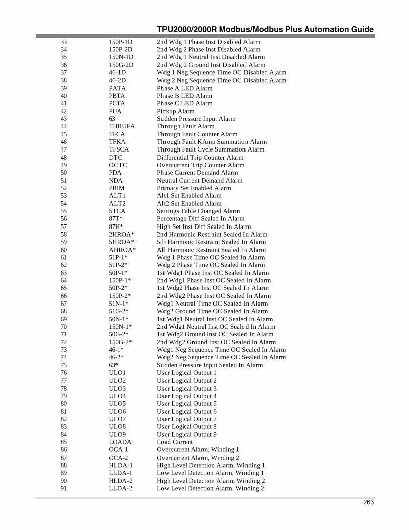
TPU2000/2000R Modbus/Modbus Plus Automation Guide
263
33 150P-1D 2nd Wdg 1 Phase Inst Disabled Alarm34 150P-2D 2nd Wdg 2 Phase Inst Disabled Alarm35 150N-1D 2nd Wdg 1 Neutral Inst Disabled Alarm36 150G-2D 2nd Wdg 2 Ground Inst Disabled Alarm37 46-1D Wdg 1 Neg Sequence Time OC Disabled Alarm38 46-2D Wdg 2 Neg Sequence Time OC Disabled Alarm39 PATA Phase A LED Alarm40 PBTA Phase B LED Alarm41 PCTA Phase C LED Alarm42 PUA Pickup Alarm43 63 Sudden Pressure Input Alarm44 THRUFA Through Fault Alarm45 TFCA Through Fault Counter Alarm46 TFKA Through Fault KAmp Summation Alarm47 TFSCA Through Fault Cycle Summation Alarm48 DTC Differential Trip Counter Alarm49 OCTC Overcurrent Trip Counter Alarm50 PDA Phase Current Demand Alarm51 NDA Neutral Current Demand Alarm52 PRIM Primary Set Enabled Alarm53 ALT1 Alt1 Set Enabled Alarm54 ALT2 Alt2 Set Enabled Alarm55 STCA Settings Table Changed Alarm56 87T* Percentage Diff Sealed In Alarm57 87H* High Set Inst Diff Sealed In Alarm58 2HROA* 2nd Harmonic Restraint Sealed In Alarm59 5HROA* 5th Harmonic Restraint Sealed In Alarm60 AHROA* All Harmonic Restraint Sealed In Alarm61 51P-1* Wdg 1 Phase Time OC Sealed In Alarm62 51P-2* Wdg 2 Phase Time OC Sealed In Alarm63 50P-1* 1st Wdg1 Phase Inst OC Sealed In Alarm64 150P-1* 2nd Wdg1 Phase Inst OC Sealed In Alarm65 50P-2* 1st Wdg2 Phase Inst OC Sealed In Alarm66 150P-2* 2nd Wdg2 Phase Inst OC Sealed In Alarm67 51N-1* Wdg1 Neutral Time OC Sealed In Alarm68 51G-2* Wdg2 Ground Time OC Sealed In Alarm69 50N-1* 1st Wdg1 Neutral Inst OC Sealed In Alarm70 150N-1* 2nd Wdg1 Neutral Inst OC Sealed In Alarm71 50G-2* 1st Wdg2 Ground Inst OC Sealed In Alarm72 150G-2* 2nd Wdg2 Ground Inst OC Sealed In Alarm73 46-1* Wdg1 Neg Sequence Time OC Sealed In Alarm74 46-2* Wdg2 Neg Sequence Time OC Sealed In Alarm75 63* Sudden Pressure Input Sealed In Alarm76 ULO1 User Logical Output 177 ULO2 User Logical Output 278 ULO3 User Logical Output 379 ULO4 User Logical Output 480 ULO5 User Logical Output 581 ULO6 User Logical Output 682 ULO7 User Logical Output 783 ULO8 User Logical Output 884 ULO9 User Logical Output 985 LOADA Load Current86 OCA-1 Overcurrent Alarm, Winding 187 OCA-2 Overcurrent Alarm, Winding 288 HLDA-1 High Level Detection Alarm, Winding 189 LLDA-1 Low Level Detection Alarm, Winding 190 HLDA-2 High Level Detection Alarm, Winding 291 LLDA-2 Low Level Detection Alarm, Winding 2
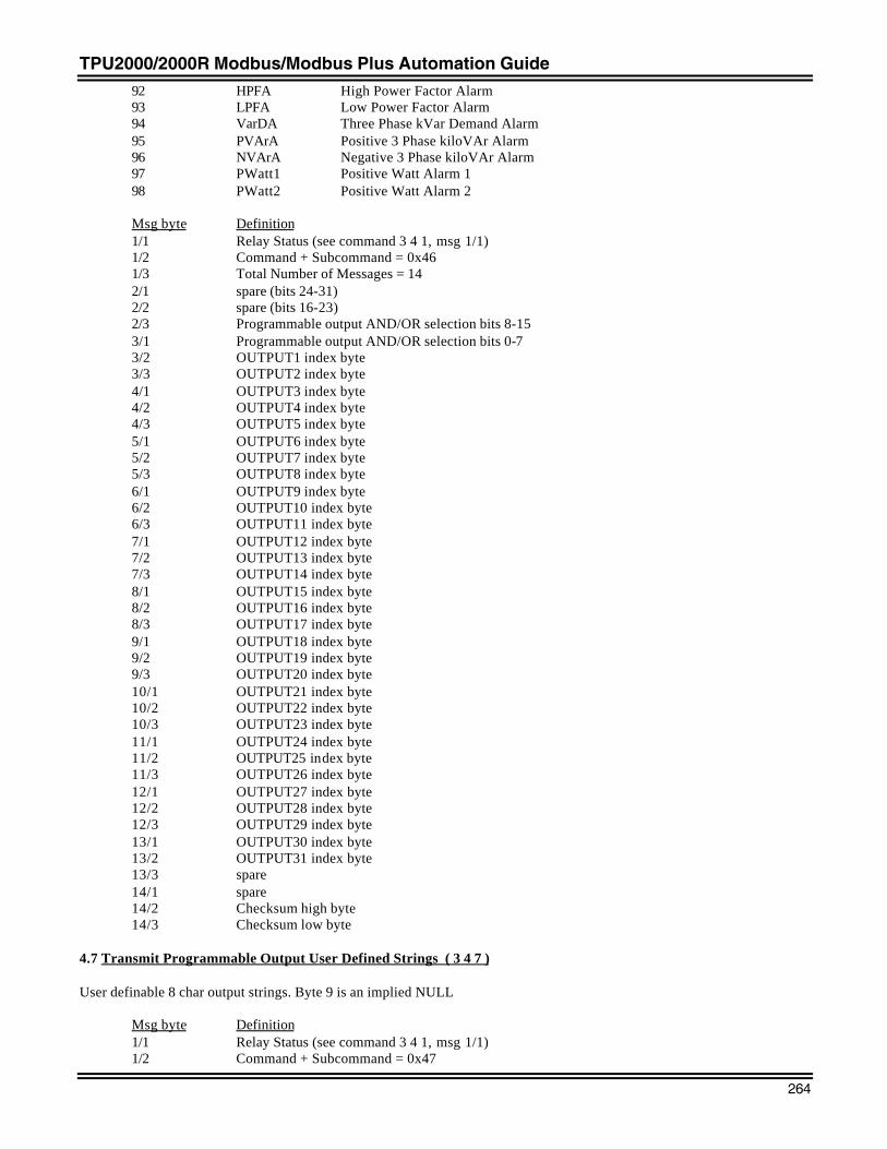
TPU2000/2000R Modbus/Modbus Plus Automation Guide
264
92 HPFA High Power Factor Alarm93 LPFA Low Power Factor Alarm94 VarDA Three Phase kVar Demand Alarm95 PVArA Positive 3 Phase kiloVAr Alarm96 NVArA Negative 3 Phase kiloVAr Alarm97 PWatt1 Positive Watt Alarm 198 PWatt2 Positive Watt Alarm 2
Msg byte Definition1/1 Relay Status (see command 3 4 1, msg 1/1)1/2 Command + Subcommand = 0x461/3 Total Number of Messages = 142/1 spare (bits 24-31)2/2 spare (bits 16-23)2/3 Programmable output AND/OR selection bits 8-153/1 Programmable output AND/OR selection bits 0-73/2 OUTPUT1 index byte3/3 OUTPUT2 index byte4/1 OUTPUT3 index byte4/2 OUTPUT4 index byte4/3 OUTPUT5 index byte5/1 OUTPUT6 index byte5/2 OUTPUT7 index byte5/3 OUTPUT8 index byte6/1 OUTPUT9 index byte6/2 OUTPUT10 index byte6/3 OUTPUT11 index byte7/1 OUTPUT12 index byte7/2 OUTPUT13 index byte7/3 OUTPUT14 index byte8/1 OUTPUT15 index byte8/2 OUTPUT16 index byte8/3 OUTPUT17 index byte9/1 OUTPUT18 index byte9/2 OUTPUT19 index byte9/3 OUTPUT20 index byte10/1 OUTPUT21 index byte10/2 OUTPUT22 index byte10/3 OUTPUT23 index byte11/1 OUTPUT24 index byte11/2 OUTPUT25 index byte11/3 OUTPUT26 index byte12/1 OUTPUT27 index byte12/2 OUTPUT28 index byte12/3 OUTPUT29 index byte13/1 OUTPUT30 index byte13/2 OUTPUT31 index byte13/3 spare14/1 spare14/2 Checksum high byte14/3 Checksum low byte
4.7 Transmit Programmable Output User Defined Strings ( 3 4 7 )
User definable 8 char output strings. Byte 9 is an implied NULL
Msg byte Definition1/1 Relay Status (see command 3 4 1, msg 1/1)1/2 Command + Subcommand = 0x47
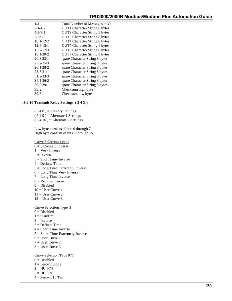
TPU2000/2000R Modbus/Modbus Plus Automation Guide
265
1/3 Total Number of Messages = 392/1-4/2 OUT1 Character String 8 bytes4/3-7/1 OUT2 Character String 8 bytes7/2-9/3 OUT3 Character String 8 bytes10/1-12/2 OUT4 Character String 8 bytes12/3-15/1 OUT5 Character String 8 bytes15/2-17/3 OUT6 Character String 8 bytes18/1-20/2 OUT7 Character String 8 bytes20/3-23/1 spare Character String 8 bytes23/2-25/3 spare Character String 8 bytes26/1-28/2 spare Character String 8 bytes28/3-31/1 spare Character String 8 bytes31/2-33/3 spare Character String 8 bytes34/1-36/2 spare Character String 8 bytes36/3-39/1 spare Character String 8 bytes39/2 Checksum high byte39/3 Checksum low byte
4.8,9,10 Transmit Relay Settings ( 3 4 X )
( 3 4 8 ) = Primary Settings( 3 4 9 ) = Alternate 1 Settings( 3 4 10 ) = Alternate 2 Settings
Low byte consists of bits 0 through 7.High byte consists of bits 8 through 15.
Curve Selection Type I0 = Extremely Inverse1 = Very Inverse2 = Inverse3 = Short Time Inverse4 = Definite Time5 = Long Time Extremely Inverse6 = Long Time Very Inverse7 = Long Time Inverse8 = Recloser Curve9 = Disabled10 = User Curve 111 = User Curve 212 = User Curve 3
Curve Selection Type II0 = Disabled1 = Standard2 = Inverse3 = Definite Time4 = Short Time Inverse5 = Short Time Extremely Inverse6 = User Curve 17 = User Curve 28 = User Curve 3
Curve Selection Type 87T0 = Disabled1 = Percent Slope2 = HU 30%3 = HU 35%4 = Percent 15 Tap
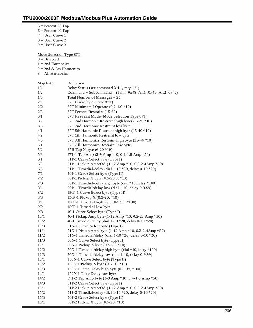
TPU2000/2000R Modbus/Modbus Plus Automation Guide
266
5 = Percent 25 Tap6 = Percent 40 Tap7 = User Curve 18 = User Curve 29 = User Curve 3
Mode Selection Type 87T0 = Disabled1 = 2nd Harmonics2 = 2nd & 5th Harmonics3 = All Harmonics
Msg byte Definition1/1 Relay Status (see command 3 4 1, msg 1/1)1/2 Command + Subcommand = (Prim=0x48, Alt1=0x49, Alt2=0x4a)1/3 Total Number of Messages = 252/1 87T Curve byte (Type 87T)2/2 87T Minimum I Operate (0.2-1.0 *10)2/3 87T Percent Restraint (15-60)3/1 87T Restraint Mode (Mode Selection Type 87T)3/2 87T 2nd Harmonic Restraint high byte(7.5-25 *10)3/3 87T 2nd Harmonic Restraint low byte4/1 87T 5th Harmonic Restraint high byte (15-40 *10)4/2 87T 5th Harmonic Restraint low byte4/3 87T All Harmonics Restraint high byte (15-40 *10)5/1 87T All Harmonics Restraint low byte 5/2 87H Tap X byte (6-20 *10)5/3 87T-1 Tap Amp (2-9 Amp *10, 0.4-1.8 Amp *50)6/1 51P-1 Curve Select byte (Type I)6/2 51P-1 Pickup Amp/OA (1-12 Amp *10, 0.2-2.4Amp *50)6/3 51P-1 Timedial/delay (dial 1-10 *20, delay 0-10 *20)7/1 50P-1 Curve Select byte (Type II)7/2 50P-1 Pickup X byte (0.5-20.0, *10)7/3 50P-1 Timedial/delay high byte (dial *10,delay *100)8/1 50P-1 Timedial/delay low (dial 1-10, delay 0-9.99)8/2 150P-1 Curve Select byte (Type II)8/3 150P-1 Pickup X (0.5-20, *10)9/1 150P-1 Timedial high byte (0-9.99, *100)9/2 150P-1 Timedial low byte9/3 46-1 Curve Select byte (Type I)10/1 46-1 Pickup Amp byte (1-12 Amp *10, 0.2-2.4Amp *50)10/2 46-1 Timedial/delay (dial 1-10 *20, delay 0-10 *20)10/3 51N-1 Curve Select byte (Type I)11/1 51N-1 Pickup Amp byte (1-12 Amp *10, 0.2-2.4Amp *50) 11/2 51N-1 Timedial/delay (dial 1-10 *20, delay 0-10 *20)11/3 50N-1 Curve Select byte (Type II)12/1 50N-1 Pickup X byte (0.5-20, *10)12/2 50N-1 Timedial/delay high byte (dial *10,delay *100)12/3 50N-1 Timedial/delay low (dial 1-10, delay 0-9.99)13/1 150N-1 Curve Select byte (Type II)13/2 150N-1 Pickup X byte (0.5-20, *10)13/3 150N-1 Time Delay high byte (0-9.99, *100)14/1 150N-1 Time Delay low byte14/2 87T-2 Tap Amp byte (2-9 Amp *10, 0.4-1.8 Amp *50)14/3 51P-2 Curve Select byte (Type I)15/1 51P-2 Pickup Amp/OA (1-12 Amp *10, 0.2-2.4Amp *50)15/2 51P-2 Timedial/delay (dial 1-10 *20, delay 0-10 *20)15/3 50P-2 Curve Select byte (Type II)16/1 50P-2 Pickup X byte (0.5-20, *10)
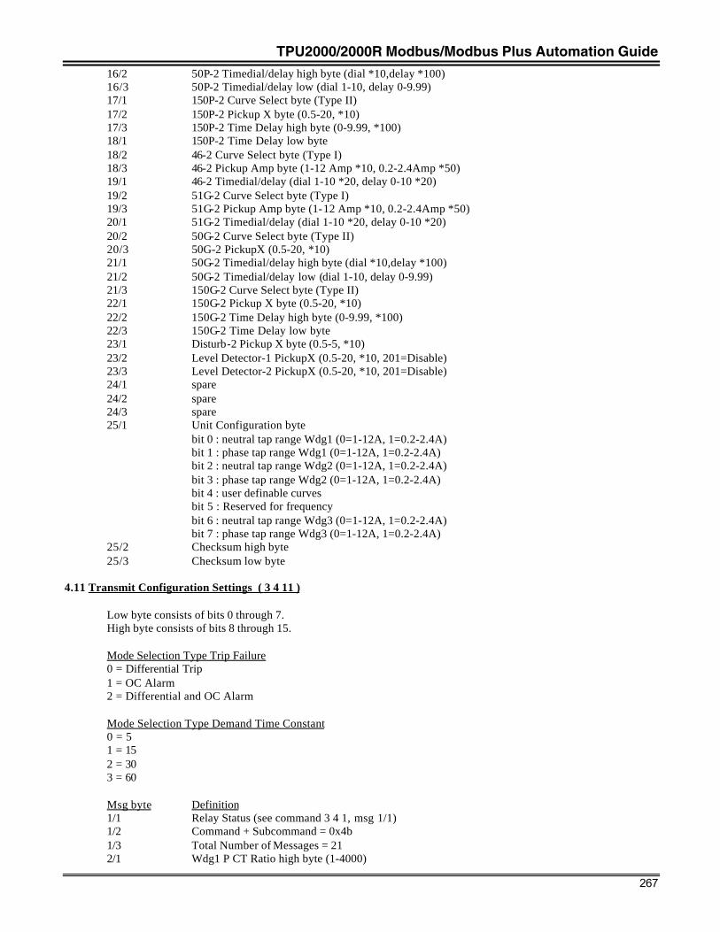
TPU2000/2000R Modbus/Modbus Plus Automation Guide
267
16/2 50P-2 Timedial/delay high byte (dial *10,delay *100)16/3 50P-2 Timedial/delay low (dial 1-10, delay 0-9.99)17/1 150P-2 Curve Select byte (Type II)17/2 150P-2 Pickup X byte (0.5-20, *10)17/3 150P-2 Time Delay high byte (0-9.99, *100)18/1 150P-2 Time Delay low byte18/2 46-2 Curve Select byte (Type I)18/3 46-2 Pickup Amp byte (1-12 Amp *10, 0.2-2.4Amp *50)19/1 46-2 Timedial/delay (dial 1-10 *20, delay 0-10 *20)19/2 51G-2 Curve Select byte (Type I)19/3 51G-2 Pickup Amp byte (1-12 Amp *10, 0.2-2.4Amp *50)20/1 51G-2 Timedial/delay (dial 1-10 *20, delay 0-10 *20)20/2 50G-2 Curve Select byte (Type II)20/3 50G-2 PickupX (0.5-20, *10)21/1 50G-2 Timedial/delay high byte (dial *10,delay *100)21/2 50G-2 Timedial/delay low (dial 1-10, delay 0-9.99)21/3 150G-2 Curve Select byte (Type II)22/1 150G-2 Pickup X byte (0.5-20, *10)22/2 150G-2 Time Delay high byte (0-9.99, *100)22/3 150G-2 Time Delay low byte23/1 Disturb-2 Pickup X byte (0.5-5, *10)23/2 Level Detector-1 PickupX (0.5-20, *10, 201=Disable)23/3 Level Detector-2 PickupX (0.5-20, *10, 201=Disable)24/1 spare24/2 spare24/3 spare25/1 Unit Configuration byte
bit 0 : neutral tap range Wdg1 (0=1-12A, 1=0.2-2.4A)bit 1 : phase tap range Wdg1 (0=1-12A, 1=0.2-2.4A)bit 2 : neutral tap range Wdg2 (0=1-12A, 1=0.2-2.4A)bit 3 : phase tap range Wdg2 (0=1-12A, 1=0.2-2.4A)bit 4 : user definable curvesbit 5 : Reserved for frequencybit 6 : neutral tap range Wdg3 (0=1-12A, 1=0.2-2.4A)bit 7 : phase tap range Wdg3 (0=1-12A, 1=0.2-2.4A)
25/2 Checksum high byte25/3 Checksum low byte
4.11 Transmit Configuration Settings ( 3 4 11 )
Low byte consists of bits 0 through 7.High byte consists of bits 8 through 15.
Mode Selection Type Trip Failure0 = Differential Trip1 = OC Alarm2 = Differential and OC Alarm
Mode Selection Type Demand Time Constant0 = 51 = 152 = 303 = 60
Msg byte Definition1/1 Relay Status (see command 3 4 1, msg 1/1)1/2 Command + Subcommand = 0x4b1/3 Total Number of Messages = 212/1 Wdg1 P CT Ratio high byte (1-4000)
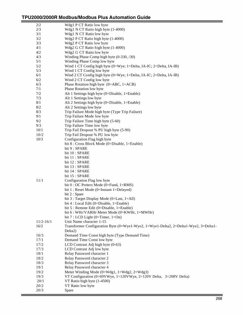
TPU2000/2000R Modbus/Modbus Plus Automation Guide
268
2/2 Wdg1 P CT Ratio low byte2/3 Wdg1 N CT Ratio high byte (1-4000)3/1 Wdg1 N CT Ratio low byte3/2 Wdg2 P CT Ratio high byte (1-4000)3/3 Wdg2 P CT Ratio low byte4/1 Wdg2 G CT Ratio high byte (1-4000)4/2 Wdg2 G CT Ratio low byte4/3 Winding Phase Comp high byte (0-330, /30)5/1 Winding Phase Comp low byte5/2 Wind 1 CT Config high byte (0=Wye; 1=Delta, IA-IC; 2=Delta, IA-IB)5/3 Wind 1 CT Config low byte6/1 Wind 2 CT Config high byte (0=Wye; 1=Delta, IA-IC; 2=Delta, IA-IB)6/2 Wind 2 CT Config low byte6/3 Phase Rotation high byte (0=ABC, 1=ACB)7/1 Phase Rotation low byte7/2 Alt 1 Settings high byte (0=Disable, 1=Enable)7/3 Alt 1 Settings low byte8/1 Alt 2 Settings high byte (0=Disable, 1=Enable)8/2 Alt 2 Settings low byte8/3 Trip Failure Mode high byte (Type Trip Failure)9/1 Trip Failure Mode low byte9/2 Trip Failure Time high byte (5-60)9/3 Trip Failure Time low byte
10/1 Trip Fail Dropout % PU high byte (5-90)10/2 Trip Fail Dropout % PU low byte10/3 Configuration Flag high byte
bit 8 : Cross Block Mode (0=Disable, 1=Enable)bit 9 : SPAREbit 10 : SPAREbit 11 : SPAREbit 12 : SPAREbit 13 : SPAREbit 14 : SPAREbit 15 : SPARE
11/1 Configuration Flag low bytebit 0 : OC Protect Mode (0=Fund, 1=RMS)bit 1 : Reset Mode (0=Instant 1=Delayed)bit 2 : Sparebit 3 : Target Display Mode (0=Last, 1=All)bit 4 : Local Edit (0=Disable, 1=Enable)bit 5 : Remote Edit (0=Disable, 1=Enable)bit 6 : WHr/VARHr Meter Mode (0=KWHr, 1=MWHr)bit 7 : LCD Light (0=Timer, 1=On)
11/2-16/1 Unit Name character 1-1516/2 Transformer Configuration Byte (0=Wye1-Wye2, 1=Wye1-Delta2, 2=Delta1-Wye2, 3=Delta1-
Delta2) 16/3 Demand Time Const high byte (Type Demand Time) 17/1 Demand Time Const low byte 17/2 LCD Contrast Adj high byte (0-63)
17/3 LCD Contrast Adj low byte18/1 Relay Password character 118/2 Relay Password character 218/3 Relay Password character 319/1 Relay Password character 419/2 Meter Winding Mode (0=Wdg1, 1=Wdg2, 2=Wdg3)19/3 VT Configuration (0=69VWye, 1=120VWye, 2=120V Delta, 3=208V Delta)
20/1 VT Ratio high byte (1-4500)20/2 VT Ratio low byte
20/3 Spare
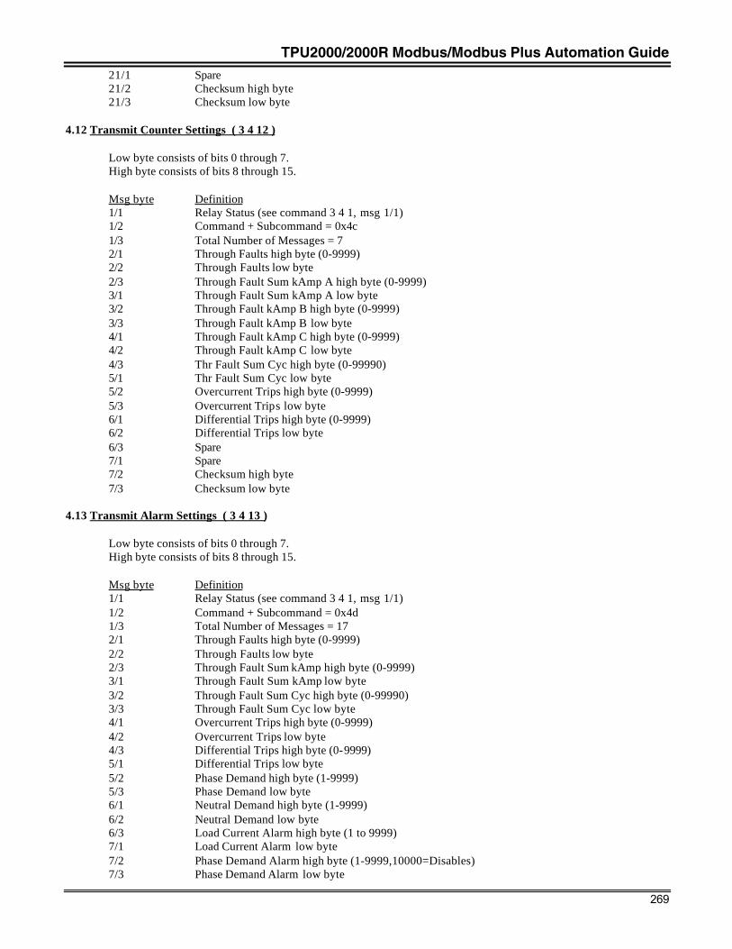
TPU2000/2000R Modbus/Modbus Plus Automation Guide
269
21/1 Spare21/2 Checksum high byte21/3 Checksum low byte
4.12 Transmit Counter Settings ( 3 4 12 )
Low byte consists of bits 0 through 7.High byte consists of bits 8 through 15.
Msg byte Definition1/1 Relay Status (see command 3 4 1, msg 1/1)1/2 Command + Subcommand = 0x4c1/3 Total Number of Messages = 72/1 Through Faults high byte (0-9999)2/2 Through Faults low byte2/3 Through Fault Sum kAmp A high byte (0-9999)3/1 Through Fault Sum kAmp A low byte3/2 Through Fault kAmp B high byte (0-9999)3/3 Through Fault kAmp B low byte4/1 Through Fault kAmp C high byte (0-9999)4/2 Through Fault kAmp C low byte4/3 Thr Fault Sum Cyc high byte (0-99990)5/1 Thr Fault Sum Cyc low byte5/2 Overcurrent Trips high byte (0-9999)5/3 Overcurrent Trips low byte6/1 Differential Trips high byte (0-9999)6/2 Differential Trips low byte6/3 Spare7/1 Spare7/2 Checksum high byte7/3 Checksum low byte
4.13 Transmit Alarm Settings ( 3 4 13 )
Low byte consists of bits 0 through 7.High byte consists of bits 8 through 15.
Msg byte Definition1/1 Relay Status (see command 3 4 1, msg 1/1)1/2 Command + Subcommand = 0x4d1/3 Total Number of Messages = 172/1 Through Faults high byte (0-9999)2/2 Through Faults low byte2/3 Through Fault Sum kAmp high byte (0-9999)3/1 Through Fault Sum kAmp low byte3/2 Through Fault Sum Cyc high byte (0-99990)3/3 Through Fault Sum Cyc low byte4/1 Overcurrent Trips high byte (0-9999)4/2 Overcurrent Trips low byte4/3 Differential Trips high byte (0-9999)5/1 Differential Trips low byte5/2 Phase Demand high byte (1-9999)5/3 Phase Demand low byte6/1 Neutral Demand high byte (1-9999)6/2 Neutral Demand low byte6/3 Load Current Alarm high byte (1 to 9999)7/1 Load Current Alarm low byte7/2 Phase Demand Alarm high byte (1-9999,10000=Disables)7/3 Phase Demand Alarm low byte
TPU2000/2000R Modbus/Modbus Plus Automation Guide
270
8/1 Low PF Alarm high byte(0.5-1.0 *100, 101=Disables)8/2 Low PF Alarm low byte8/3 High PF Alarm high byte(0.5-1.0 *100, 101=Disables)9/1 High Pf Alarm low byte9/2 Positive kVAR Alarm high byte (10-99990 / 10,10000=Disable)9/3 Positive kVAR Alarm low byte10/1 Negative kVAR Alarm high byte (10-99990 /10,10000=Disable)10/2 Negative kVAR Alarm high byte10/3 Pos Watt Alarm 1 high byte (1-9999, 10000=Disable)11/1 Pos Watt Alarm 1 low byte11/2 Pos Watt Alarm 2 high byte (1-9999, 10000=Disable)11/3 Pos Watt Alarm 2 low byte12/1 Spare12/2 Spare12/3 Spare13/1 Spare13/2 Spare13/3 Spare14/1 Spare14/2 Spare14/3 Spare15/1 Spare15/2 Spare15/3 Spare16/1 Spare16/2 Spare16/3 Spare17/1 Spare17/2 Checksum high byte17/3 Checksum low byte
4.14 Transmit Real Time Clock ( 3 4 14 )
Msg byte Definition 1/1 Relay Status (see command 3 4 1, msg 1/1) 1/2 Command + Subcommand = 0x4e 1/3 Total Number of Messages = 4 2/1 Hours byte (0-23) 2/2 Minutes byte (0-59) 2/3 Seconds byte (0-59) 3/1 Day byte (0-31), (0=Shutdown Clock) 3/2 Month byte (1-12) 3/3 Year byte (0-99) 4/1 Spare 4/2 Checksum high byte 4/3 Checksum low byte
4.15 Transmit Programmable Output Delays ( 3 4 15 )
Msg Byte Definition 1/1 Relay Status (see command 3 4 1, msg 1/1) 1/2 Command + Subcommand = 0x4f 1/3 Total Number of Messages = 8 2/1 OUT 5 delay high byte (0.00-60, *100) 2/2 OUT 5 delay low byte 2/3 OUT 7 delay high byte (0.00-60, *100) 3/1 OUT 7 delay low byte
3/2 OUT 4 delay high byte (0.00-60, *100) 3/3 OUT 4 delay low byte
TPU2000/2000R Modbus/Modbus Plus Automation Guide
271
4/1 OUT 6 delay high byte (0.00-60, *100) 4/2 OUT 6 delay low byte 4/3 OUT 3 delay high byte (0.00-60, *100) 5/1 OUT 3 delay low byte 5/2 OUT 2 delay high byte (0.00-60, *100) 5/3 OUT 2 delay low byte
6/1 OUT 1 delay high byte (0.00-60, *100) 6/2 OUT 1 delay low byte 6/3 Spare 7/1 Spare 7/2 Spare 7/3 Spare 8/1 Spare 8/2 Checksum high byte 8/3 Checksum low byte
5 Transmit Buffer "N" Commands ( 3 5 n )
When n=0 then the previous Receive Number command would define the number "N". Otherwise this command would takethe number "N" defined by the subcmd field (1 - 15 ).
N Definition0 Reserved for repeat 3 5 n1 Show Wdg 1 & 2 Load Metered Data2 Show Demand Currents Data3 Show Max Demand Currents Data4 Show Min Demand Currents Data5 Show Magnitudes Load Meter Data6 Show Average Load Current7 Show Wdg 1 & 2 Differential Meter Data8 Send First Fault Record9 Send Next Fault Record10 Not used11 Not used12 Send First Operation Record13 Send Next Operation Record14 Breaker Status (including contact inputs)15 Power Fail Data
5.1 Show Wdg 1 & 2 Load Metered Data ( 3 5 1 )
Msg byte Definition 1/1 Relay Status (see command 3 4 1, msg 1/1) 1/2 Command + Subcommand = 0x51 1/3 Total Number of Messages = 29 2/1 Aux. Status byte (Meter Mode)
Bits 0 & 1 : 0=Winding1; 1=Winding2; 2=Winding3 Bit 2 : 0 = Wye PTs; 1 = Delta PTs Bit 3 : 0 = kWhr; 1 = MWhr
2/2 IA-1 Hi byte (Load Currents) 2/3 IA-1 Mid byte 3/1 IA-1 Lo byte 3/2 IA-1 Angle Hi byte 3/3 IA-1 Angle Lo byte 4/1 IB-1 Hi byte 4/2 IB-1 Mid byte 4/3 IB-1 Lo byte 5/1 IB-1 Angle Hi byte 5/2 IB-1 Angle Lo byte
TPU2000/2000R Modbus/Modbus Plus Automation Guide
272
5/3 IC-1 Hi byte 6/1 IC-1 Mid byte 6/2 IC-1 Lo byte 6/3 IC-1 Angle Hi byte 7/1 IC-1 Angle Lo byte 7/2 IN-1 Hi byte 7/3 IN-1 Mid byte 8/1 IN-1 Lo byte 8/2 IN-1 Angle Hi byte 8/3 IN-1 Angle Lo byte 9/1 I0-1 (Mag) Hi byte 9/2 I0-1 (Mag) Mid byte 9/3 I0-1 (Mag) Lo byte 10/1 I0-1 Angle Hi byte 10/2 I0-1 Angle Lo byte 10/3 I1-1 (Mag) Hi byte 11/1 I1-1 (Mag) Mid byte 11/2 I1-1 (Mag) Lo byte 11/3 I1-1 Angle Hi byte
12/1 I1-1 Angle Lo byte 12/2 I2-1 (Mag) Hi byte
12/3 I2-1 (Mag) Mid byte 13/1 I2-1 (Mag) Lo byte 13/2 I2-1 Angle Hi byte 13/3 I2-1 Angle Lo byte 14/1 IA-2 Hi byte 14/2 IA-2 Mid byte 14/3 IA-2 Lo byte 15/1 IA-2 Angle Hi byte 15/2 IA-2 Angle Hi byte 15/3 IB-2 Hi byte 16/1 IB-2 Mid byte 16/2 IB-2 Lo byte 16/3 IB-2 Angle Hi byte 17/1 IB-2 Angle Lo byte 17/2 IC-2 Hi byte 17/3 IC-2 Mid byte 18/1 IC-2 Lo byte 18/2 IC-2 Angle Hi byte 18/3 IC-2 Angle Lo byte 19/1 IG-2 Hi byte 19/2 IG-2 Mid byte 19/3 IG-2 Lo byte 20/1 IG-2 Angle Hi byte 20/2 IG-2 Angle Lo byte 20/3 I0-2 (Mag) Hi byte 21/1 I0-2 (Mag) Mid byte 21/2 I0-2 (Mag) Lo byte 21/3 I0-2 Angle Hi byte 22/1 I0-2 Angle Lo byte 22/2 I1-2 (Mag) Hi byte 22/3 I1-2 (Mag) Mid byte 23/1 I1-2 (Mag) Lo byte 23/2 I1-2 Angle Hi byte 23/3 I1-2 Angle Lo byte 24/1 I2-2 (Mag) Hi byte 24/2 I2-2 (Mag) Mid byte 24/3 I2-2 (Mag) Lo byte 25/1 I2-2 Angle Hi byte
TPU2000/2000R Modbus/Modbus Plus Automation Guide
273
25/2 I2-2 Angle Lo byte 25/3 Spare 26/1-29/3 Reserved for Tap Changer Position
5.2 Show Demand Currents Data ( 3 5 2 )
Msg byte Definition 1/1 Relay Status (see command 3 4 1, msg 1/1) 1/2 Command + Subcommand = 0x52 1/3 Total Number of Messages = 6 2/1 Aux. Status byte (see command 3 5 1, msg 2/1) 2/2 Demand Ia Hi byte (Load Currents) 2/3 Demand Ia Mid byte 3/1 Demand Ia Lo byte 3/2 Demand Ib Hi byte 3/3 Demand Ib Mid byte 4/1 Demand Ib Lo byte 4/2 Demand Ic Hi byte 4/3 Demand Ic Mid byte 5/1 Demand Ic Lo byte 5/2 Demand In/Ig Hi byte 5/3 Demand In/Ig Mid byte 6/1 Demand In/Ig Lo byte 6/2 Spare 6/3 Spare
5.3 Show Maximum Demand Currents Data ( 3 5 3 )
Msg byte Definition 1/1 Relay Status (see command 3 4 1, msg 1/1) 1/2 Command + Subcommand = 0x53 1/3 Total Number of Messages = 12 2/1 Aux. Status byte (see command 3 5 1, msg 2/1) 2/2 Max Dem Ia Hi byte (Load Currents) 2/3 Max Dem Ia Mid byte 3/1 Max Dem Ia Lo byte 3/2 Max Dem Ia time yy 3/3 Max Dem Ia time mn 4/1 Max Dem Ia time dd 4/2 Max Dem Ia time hh 4/3 Max Dem Ia time mm 5/1 Max Dem Ib Hi byte 5/2 Max Dem Ib Mid byte 5/3 Max Dem Ib Lo byte 6/1 Max Dem Ib time yy 6/2 Max Dem Ib time mn 6/3 Max Dem Ib time dd 7/1 Max Dem Ib time hh 7/2 Max Dem Ib time mm 7/3 Max Dem Ic Hi byte 8/1 Max Dem Ic Mid byte 8/2 Max Dem Ic Lo byte 8/3 Max Dem Ic time yy 9/1 Max Dem Ic time mn 9/2 Max Dem Ic time dd 9/3 Max Dem Ic time hh 10/1 Max Dem Ic time mm 10/2 Max Dem In/Ig Hi byte 10/3 Max Dem In/Ig Mid byte
TPU2000/2000R Modbus/Modbus Plus Automation Guide
274
11/1 Max Dem In/Ig Lo byte 11/2 Max Dem In/Ig time yy 11/3 Max Dem In/Ig time mn
12/1 Max Dem In/Ig time dd 12/2 Max Dem In/Ig time hh 12/3 Max Dem In/Ig time mm
5.4 Show Minimum Demand Currents Data ( 3 5 4 )
Msg byte Definition 1/1 Relay Status (see command 3 4 1, msg 1/1) 1/2 Command + Subcommand = 0x53 1/3 Total Number of Messages = 12 2/1 Aux. Status byte (see command 3 5 1, msg 2/1) 2/2 Min Dem Ia Hi byte (Load Currents) 2/3 Min Dem Ia Mid byte 3/1 Min Dem Ia Lo byte 3/2 Min Dem Ia time yy 3/3 Min Dem Ia time mn 4/1 Min Dem Ia time dd 4/2 Min Dem Ia time hh 4/3 Min Dem Ia time mm 5/1 Min Dem Ib Hi byte 5/2 Min Dem Ib Mid byte 5/3 Min Dem Ib Lo byte 6/1 Min Dem Ib time yy 6/2 Min Dem Ib time mn 6/3 Min Dem Ib time dd 7/1 Min Dem Ib time hh 7/2 Min Dem Ib time mm 7/3 Min Dem Ic Hi byte 8/1 Min Dem Ic Mid byte 8/2 Min Dem Ic Lo byte 8/3 Min Dem Ic time yy 9/1 Min Dem Ic time mn 9/2 Min Dem Ic time dd 9/3 Min Dem Ic time hh 10/1 Min Dem Ic time mm 10/2 Min Dem In/Ig Hi byte 10/3 Min Dem In/Ig Mid byte 11/1 Min Dem In/Ig Lo byte 11/2 Min Dem In/Ig time yy 11/3 Min Dem In/Ig time mn 12/1 Min Dem In/Ig time dd 12/2 Min Dem In/Ig time hh 12/3 Min Dem In/Ig time mm
5.5 Show Magnitudes Load Metered Data ( 3 5 5 )
Msg byte Definition 1/1 Relay Status (see command 3 4 1, msg 1/1) 1/2 Command + Subcommand = 0x55 1/3 Total Number of Messages = 6 2/1 Aux. Status byte (see command 3 5 1, msg 2/1) 2/2 Ia high byte (Load Currents) 2/3 Ia (mid byte) 3/1 Ia (low byte) 3/2 Ib (high byte) 3/3 Ib (mid byte)
TPU2000/2000R Modbus/Modbus Plus Automation Guide
275
4/1 Ib (low byte) 4/2 Ic (high byte) 4/3 Ic (mid byte) 5/1 Ic (low byte) 5/2 In/Ig (high byte) 5/3 In/Ig (mid byte) 6/1 In/Ig (low byte) 6/2 Spare 6/3 Spare
5.6 Show Average Load Current ( 3 5 6 )
Msg byte Definition 1/1 Relay Status (see command 3 4 1, msg 1/1) 1/2 Command + Subcommand = 0x56 1/3 Total Number of Messages = 3 2/1 Aux. Status byte (see command 3 5 1, msg 2/1) 2/2 Iavg (high byte) 2/3 Iavg (mid byte) 3/1 Iavg (low byte) 3/2 Spare 3/3 Spare
5.7 Show Wdg 1 & 2 Differential Metering ( 3 5 7 )
Msg byte Definition 1/1 Relay Status (see command 3 4 1, msg 1/1) 1/2 Command + Subcommand = 0x57 1/3 Total Number of Messages = 18 2/1 Aux. Status (see command 3 5 1, msg 2/1) 2/2 Iop A high byte (*800) 2/3 Iop A low byte 3/1 Iop B high byte (*800) 3/2 Iop B low byte 3/3 Iop C high byte (*800) 4/1 Iop C low byte 4/2 IresA-1 high byte (*800) 4/3 IresA-1 low byte 5/1 IresA-1 Angle high byte 5/2 IresA-1 Angle low byte 5/3 IresB-1 high byte (*800) 6/1 IresB-1 low byte 6/2 IresB-1 Angle high byte 6/3 IresB-1 Angle low byte 7/1 IresC-1 high byte (*800) 7/2 IresC-1 low byte 7/3 IresC-1 Angle high byte 8/1 IresC-1 Angle low byte 8/2 IresA-2 high byte (*800) 8/3 IresA-2 low byte 9/1 IresA-2 Angle high byte 9/2 IresA-2 Angle low byte 9/3 IresB-2 high byte (*800) 10/1 IresB-2 low byte 10/2 IresB-2 Angle high byte 10/3 IresB-2 Angle low byte 11/1 IresC-2 high byte (*800) 11/2 IresC-2 low byte 11/3 IresC-2 Angle high byte
TPU2000/2000R Modbus/Modbus Plus Automation Guide
276
12/1 IresC-2 Angle low byte 12/2 2nd Harmonic % A-1 byte (*2) 12/3 2nd Harmonic % B-1 byte (*2) 13/1 2nd Harmonic % C-1 byte (*2) 13/2 2nd Harmonic % A-2 byte (*2) 13/3 2nd Harmonic % B-2 byte (*2) 14/1 2nd Harmonic % C-2 byte (*2) 14/2 5th Harmonic % A-1 byte (*2) 14/3 5th Harmonic % B-1 byte (*2) 15/1 5th Harmonic % C-1 byte (*2) 15/2 5th Harmonic % A-2 byte (*2) 15/3 5th Harmonic % B-2 byte (*2) 16/1 5th Harmonic % C-2 byte (*2) 16/2 All Harmonics % A-1 byte (*2) 16/3 All Harmonics % B-1 byte (*2) 17/1 All Harmonics % C-1 byte (*2) 17/2 All Harmonics % A-2 byte (*2) 17/3 All Harmonics % B-2 byte (*2) 18/1 All Harmonics % C-2 byte (*2) 18/2 Winding 1 Tap (*10) 18/3 Winding 2 Tap (*10)
5.8 Send First Differential Fault Record ( 3 5 8 )
The Differential Fault Record command returns data in two parts. This command requires a data byte message to indicatewhich part of the record is to be returned. If the data message 1/2 = 0, part 1 of the record is returned. If the data message1/2 = 1, part 2 of the record is returned.
Fault Type Definitions00 87T01 87H02 51P-103 51N-104 50P-105 50N-106 150P-107 150N-108 46-109 51P-210 51G-211 50P-212 50G-213 150P-214 150G-215 46-216 ECI-117 ECI-218 Thru Flt19 Harm Rest
Data byte 1/1 0 = Reserved for Unreported Records 1/2 0 = Send part 1 of Record, 1 = Send part 2 of Record 1/3 Checksum 1/1 + 1/2
Msg byte Definition-Part 1 of Record 1/1 Relay Status (see command 3 4 1, msg 1/1) 1/2 Command + Subcommand = 0x58 1/3 Total Number of Messages = 28
TPU2000/2000R Modbus/Modbus Plus Automation Guide
277
2/1 Param Flag high byte 2/2 Param Flag low byte 2/3 Fault Type (element) 3/1 Setting 3/2 Fault Number (high byte) 3/3 Fault Number (low byte) 4/1 Year 4/2 Month 4/3 Day 5/1 Hours 5/2 Minutes 5/3 Seconds 6/1 Hundredths of seconds 6/2 Clear Time Hi byte (*1000) 6/3 Clear Time Lo byte 7/1 Winding1 Tap Hi byte (*10) 7/2 Winding1 Tap Lo byte 7/3 Winding2 Tap Hi byte (*10) 8/1 Winding2 Tap Lo byte 8/2 I operate A Hi byte (*800) 8/3 I operate A Lo byte 9/1 I operate B Hi byte (*800) 9/2 I operate B Lo byte 9/3 I operate C Hi byte (*800) 10/1 I operate C Lo byte 10/2 I restraint A-1 Hi byte (*800) 10/3 I restraint A-1 Lo byte 11/1 I restraint B-1 Hi byte (*800) 11/2 I restraint B-1 Lo byte 11/3 I restraint C-1 Hi byte (*800) 12/1 I restraint C-1 Lo byte 12/2 I restraint A-2 Hi byte (*800) 12/3 I restraint A-2 Lo byte 13/1 I restraint B-2 Hi byte (*800) 13/2 I restraint B-2 Lo byte 13/3 I restraint C-2 Hi byte (*800) 14/1 I restraint C-2 Lo byte 14/2 2nd Harmonic A-1 (*2) 14/3 5th Harmonic A-1 (*2) 15/1 All Harmonics A-1 (*2) 15/2 2nd Harmonic B-1 (*2) 15/3 5th Harmonic B-1 (*2) 16/1 All Harmonics B-1 (*2) 16/2 2nd Harmonic C-1 (*2) 16/3 5th Harmonic C-1 (*2) 17/1 All Harmonics C-1 (*2) 17/2 2nd Harmonic A-2 (*2) 17/3 5th Harmonic A-2 (*2) 18/1 All Harmonics A-2 (*2) 18/2 2nd Harmonic B-2 (*2) 18/3 5th Harmonic B-2 (*2) 19/1 All Harmonic B-2 (*2) 19/2 2nd Harmonic C-2 (*2) 19/3 5th Harmonic C-2 (*2) 20/1 All Harmonic C-2 (*2) 20/2 I restraint A-1 (Ang) Hi byte 20/3 I restraint A-1 (Ang) Lo byte 21/1 I restraint B-1 (Ang) Hi byte 21/2 I restraint B-1 (Ang) Lo byte
TPU2000/2000R Modbus/Modbus Plus Automation Guide
278
21/3 I restraint C-1 (Ang) Hi byte 22/1 I restraint C-1 (Ang) Lo byte 22/2 I restraint A-2 (Ang) Hi byte 22/3 I restraint A-2 (Ang) Lo byte 23/1 I restraint B-2 (Ang) Hi byte 23/2 I restraint B-2 (Ang) Lo byte 23/3 I restraint C-2 (Ang) Hi byte 24/1 I restraint C-2 (Ang) Lo byte 24/2 Spare 24/3 Spare 25/1 Spare 25/2 Spare 25/3 Spare 26/1 Spare 26/2 Spare 26/3 Spare 27/1 Spare 27/2 Spare 27/3 Spare 28/1 Spare 28/2 Spare 28/3 Spare
Data byte See previous
Msg byte Definition-Part 2 of Record 1/1 Relay Status (see command 3 4 1, msg 1/1) 1/2 Command + Subcommand = 0x58 1/3 Total Number of Messages = 28 2/1 Param Flag high byte 2/2 Param Flag low byte 2/3 Fault Type (element) 3/1 Setting 3/2 Fault Number (high byte) 3/3 Fault Number (low byte) 4/1 Year 4/2 Month 4/3 Day 5/1 Hours 5/2 Minutes 5/3 Seconds 6/1 Hundredths of seconds 6/2 Clear Time Hi byte (*1000) 6/3 Clear Time Lo byte 7/1 I A-1 high byte (*800 / Phase Wdg1 Scale) 7/2 I A-1 low byte 7/3 I B-1 high byte (*800 / Phase Wdg1 Scale) 8/1 I B-1 low byte 8/2 I C-1 high byte (*800 / Phase Wdg1 Scale) 8/3 I C-1 low byte
9/1 I N-1 high byte (*800 / Neutral Wdg1 Scale) 9/2 I N-1 low byte 9/3 I A-2 high byte (*800 / Phase Wdg2 Scale) 10/1 I A-2 low byte 10/2 I B-2 high byte (*800 / Phase Wdg2 Scale) 10/3 I B-2 low byte 11/1 I C-2 high byte (*800 / Phase Wdg2 Scale) 11/2 I C-2 low byte
TPU2000/2000R Modbus/Modbus Plus Automation Guide
279
11/3 I G-2 high byte (*800 / Ground Wdg2 Scale) 12/1 I G-2 low byte 12/2 Spare 12/3 I A-1 (ang) high byte 13/1 I A-1 (ang) low byte 13/2 I B-1 (ang) high byte 13/3 I B-1 (ang) low byte 14/1 I C-1 (ang) high byte 14/2 I C-1 (ang) low byte 14/3 I N-1 (ang) high byte 15/1 I N-1 (ang) low byte 15/2 I A-2 (ang) high byte 15/3 I A-2 (ang) low byte 16/1 I B-2 (ang) high byte 16/2 I B-2 (ang) low byte 16/3 I C-2 (ang) high byte 17/1 I C-2 (ang) low byte 17/2 I G-2 (ang) high byte 17/3 I G-2 (ang) low byte 18/1 I 0-1 high byte (*800 / Phase Wdg1 Scale) 18/2 I 0-1 low byte 18/3 I 1-1 high byte (*800 / Phase Wdg1 Scale) 19/1 I 1-1 low byte 19/2 I 2-1 high byte (*800 / Phase Wdg1 Scale) 19/3 I 2-1 low byte 20/1 I 0-2 high byte (*800 / Phase Wdg2 Scale) 20/2 I 0-2 low byte 20/3 I 1-2 high byte (*800 / Phase Wdg2 Scale) 21/1 I 1-2 low byte 21/2 I 2-2 high byte (*800 / Phase Wdg2 Scale) 21/3 I 2-2 low byte 22/1 I 0-1 (ang) high byte 22/2 I 0-1 (ang) low byte 22/3 I 1-1 (ang) high byte 23/1 I 1-1 (ang) low byte 23/2 I 2-1 (ang) high byte 23/3 I 2-1 (ang) low byte 24/1 I 0-2 (ang) high byte 24/2 I 0-2 (ang) low byte 24/3 I 1-2 (ang) high byte 25/1 I 1-2 (ang) low byte 25/2 I 2-2 (ang) high byte 25/3 I 2-2 (ang) low byte 26/1 Scale - Phase Wdg 1 high byte 26/2 Scale - Phase Wdg 1 low byte 26/3 Scale - Phase Wdg 2 high byte 27/1 Scale - Phase Wdg 2 low byte 27/2 Scale - Neutral Wdg 1 high byte 27/3 Scale - Neutral Wdg 1 low byte 28/1 Scale - Ground Wdg 2 high byte 28/2 Scale - Ground Wdg 2 low byte
28/3 Spare
If no fault data entry is present then send all 0s for 2/1 through 27/3.
5.9 Send Next Differential Fault Record ( 3 5 9 )
Same format as ( 3 5 8 ) except Msg 1/2 = 0x59.
TPU2000/2000R Modbus/Modbus Plus Automation Guide
280
5.12 Send First Operations Record ( 3 5 12 )
Message Number Definitions00 87T Trip01 87H Trip02 51P-1 Trip03 51N-1 Trip04 50P-1 Trip05 50N-1 Trip06 150P-1 Trip07 150N-1 Trip08 46-1 Trip09 51P-2 Trip10 51G-2 Trip11 50P-2 Trip12 50G-2 Trip13 150P-2 Trip14 150G-2 Trip15 46-2 Trip16 ECI-117 ECI-218 Thru Flt19 Harm Rest
31 Fault Clear Failed32 Fault Cleared33 Harmonic Restraint34 Manual Trip35 Manual Trip Failed40 87T Enabled41 87H Enabled42 51P-1 Enabled43 51P-2 Enabled44 51N-1 Enabled45 51G-2 Enabled46 50P-1 Enabled47 50P-2 Enabled48 50N-1 Enabled49 50G-2 Enabled50 150P-1 Enabled51 150P-2 Enabled52 150N-1 Enabled53 150G-2 Enabled54 46-1 Enabled55 46-2 Enabled56 ALT1 Input Closed57 ALT2 Input Closed58 Event Cap1 Init59 Event Cap2 Init60 Wave Cap. Init61 Trip Input Closed62 SPR Input Closed63 TCM Input Closed64 Primary Set Active65 Alt1 Set Active66 Alt2 Set Active70 Thru Flt Cntr Alm71 Thru Flt kASum Alm72 Thru Flt Cycle Alm
TPU2000/2000R Modbus/Modbus Plus Automation Guide
281
73 OC Trip Cntr Alarm74 Diff Trip Cntr Alm75 Phase Demand Alarm76 Neutral Demand Alm77 Load Current Alarm78 Trip Coil Failure79 High PF Alarm80 Low PF Alarm81 kVAR Demand Alarm82 Pos. kVAR Alarm83 Neg. kVAR Alarm84 Pos. Watt Alarm 185 Pos. Watt Alarm 290 Event Capture #191 Event Capture #292 Waveform Capture93 High Level Detection Alarm, Wdg 194 Low Level Detection Alarm, Wdg 195 High Level Detection Alarm, Wdg 296 Low Level Detection Alarm, Wdg 2100 ROM Failure101 RAM Failure102 Self Test Failed103 EEPROM Failure104 BATRAM Failure105 DSP Failure106 Control Power Fail107 Editor Access120 87T Disabled121 87H Disabled122 51P-1 Disabled123 51P-2 Disabled124 51N-1 Disabled125 51G-2 Disabled126 50P-1 Disabled127 50P-2 Disabled128 50N-1 Disabled129 50G-2 Disabled130 150P-1 Disabled131 150P-2 Disabled132 150N-1 Disabled133 150G-2 Disabled134 46-1 Disabled135 46-2 Disabled136 ALT1 Input Opened137 ALT2 Input Opened138 Event Cap1 Reset139 Event Cap2 Reset140 Wave Cap. Reset141 Trip Input Opened142 SPR Input Opened143 TCM Input Opened162 ULI1 Input Closed163 ULI1 Input Opened164 ULI2 Input Closed165 ULI2 Input Opened
166 ULI3 Input Closed167 ULI3 Input Opened
168 ULI4 Input Closed
TPU2000/2000R Modbus/Modbus Plus Automation Guide
282
169 ULI4 Input Opened170 ULI5 Input Closed171 ULI5 Input Opened
172 ULI6 Input Closed173 ULI6 Input Opened
174 ULI7 Input Closed175 ULI7 Input Opened176 ULI8 Input Closed177 ULI8 Input Opened178 ULI9 Input Closed179 ULI9 Input Opened180 CRI Input Closed181 CRI Input Opened
Msg byte Definition 1/1 Relay Status (see command 3 4 1, msg 1/1) 1/2 Command + Subcommand = 0x5c 1/3 Total Number of Messages = 5 2/1 Year 2/2 Month 2/3 Day 3/1 Hour 3/2 Minute 3/3 Second 4/1 Hundredths of second 4/2 Message Number 4/3 Value (if any) Hi byte 5/1 Value (if any) Lo byte 5/2 Operation Number (high byte) 5/3 Operation Number (low byte)
If the operation entry doesn't exist then send 0's in all the bytes 2/1 through 5/3.
5.13 Send Next Operations Record ( 3 5 13 )
Same format as ( 3 5 12 ) except Msg 1/2 = 0x5d.
5.14 Breaker Status (Including I/O Status) ( 3 5 14 )
Input status bit 0=opened, 1=closed.Output status bit 0=de-energized, 1=energized.
Msg byte Definition 1/1 Relay Status (see command 3 4 1, msg 1/1) 1/2 Command + Subcommand = 0x5e 1/3 Total Number of Messages = 3 2/1 Contact Input Status (high byte)
Bit 0 - Input 9 Bit 1 - Spare Bit 2 - Spare Bit 3 - Spare Bit 4 - Spare Bit 5 - Spare Bit 6 - Spare Bit 7 - Spare
2/2 Contact Input Status (low byte) Bit 0 - Input 1 Bit 1 - Input 2 Bit 2 - Input 3
TPU2000/2000R Modbus/Modbus Plus Automation Guide
283
Bit 3 - Input 4 Bit 4 - Input 5 Bit 5 - Input 6 Bit 6 - Input 7 Bit 7 - Input 8
2/3 Self Test Status (high byte) Bit 0 - DSP ROM Bit 1 - DSP Internal RAM Bit 2 - DSP External RAM Bit 3 - ADC Failure Bit 4 - DSP +/-5V Bit 5 - DSP +/-15V Bit 6 - DSP +5V Bit 7 - DSP Comm. Failure
3/1 Self Test Status (low byte) Bit 0 - CPU RAM Bit 1 - CPU EPROM Bit 2 - CPU NVRAM Bit 3 - CPU EEPROM Bit 4 - Bit 5 - Bit 6 - Bit 7 -
3/2 Output Contact Status (high byte) Bit 0 - Spare Bit 1 - Spare Bit 2 - Spare Bit 3 - Spare Bit 4 - Spare Bit 5 - Spare Bit 6 - Spare Bit 7 - Spare
3/3 Output Contact Status (low byte) Bit 0 - Trip Bit 1 - Output 1 Bit 2 - Output 2 Bit 3 - Output 3 Bit 4 - Output 4 Bit 5 - Output 5 Bit 6 - Output 6 Bit 7 - Output 7
5.15 Power Fail Data ( 3 5 15 )
Msg byte Definition 1/1 Relay Status (see command 3 4 1, msg 1/1) 1/2 Command + Subcommand = 0x5f 1/3 Total Number of Messages = 4 2/1 Year 2/2 Month 2/3 Day 3/1 Hour 3/2 Minute 3/3 Second 4/1 Hundredths of second 4/2 Power Fail Type
Bit 0: DC Control Bit 1: +5/+15V
4/3 Breaker Status (state)
TPU2000/2000R Modbus/Modbus Plus Automation Guide
284
6 Load Profile Commands & Records ( 3 6 n )
N Definition0 Define Load Profile Settings1 Start Load Profile Data Accumulation2 Freeze Load Profile Data3 Report Load Profile Header-All4 Report Next Load Profile Data Block5 Retransmit Last Load Profile Data Block6 Report Load Profile Header-Last7 Not in use8 Fault Record-First9 Fault Record-Next10 Restraint Record-First11 Restraint Record-Next12 Oldest Unreported Differential Record13 Oldest Unreported Through Fault Record14 Oldest Unreported Harmonic Restraint Record15 Oldest Unreported Operations Record
6.0 Load Profile Settings ( 3 6 0 )
Reserved for user configuration.
6.1 Accumulate Load Profile Data ( 3 6 1 )
6.2 Freeze Load Profile Data ( 3 6 2 )
6.3 Report Load Profile Data Header(All Data) ( 3 6 3 )
This command is used to initialize the unit to report the entire contents of the accumulated load profile.
Msg byte Definition 1/1 Relay Status (see command 3 4 1, msg 1/1) 1/2-4/1 Report Column (1-9) Attribute Number 4/2 spare 4/3-9/3 Unit Id Name (16 chars)10/1-11/2 Time Tag of the first Block reporting (5 bytes :yy,mn,dd,hh,mm in order)11/3 spare12/1-12/2 Report Column 1 Attribute Scale(high, low byte)12/3-17/3 Report Column (2-9) Attribute Scale
Attr# Description Dynamic Scale0 Demand Ia 11 Demand Ib 12 Demand Ic 13 Demand In 1
6.4 Report Next Load Profile Data Block ( 3 6 4 )
Msg byte Definition 1/1 Demand Interval (5/15/30/60 Mins) 1/2-1/3 Record # (a number starting from 1 to #of blocks) 2/1 Total Number Data Bytes (1 through 126) 2/2-3/3 Time Tag of the first Block (5 bytes : hh, mm, dd, mn, yy in order)
NOTE: Different order from command 3 6 3 time stamp. 4/1-45/3 Data Blocks (up to 126 bytes of data)
TPU2000/2000R Modbus/Modbus Plus Automation Guide
285
Each data block is a two byte word that has the following bit configuration:bit 0-13 : data valuesbit 14 : sign bit (1=multiply bits 0-13 by -1)bit 15 : scale bit (0=multiply bits 0-13 by 1, 1=multiply bits 0-13 by attribute scale)
Example: Report column 1 is profiling attribute #0 (Demand kW-A) and has a dynamic scale = 122
Data word Binary pattern Scale Reported value8,000 0001111101000000 1 8,000 kW24,384 0101111101000000 -1 -8,000 kW16,776 0100000011000100 122 23,912 kW49,384 1100000011000100 -122 -23,912 kW
To obtain the reported value column from the data word, a listing for a c routine should look as follows:
long int ConvertData( unsigned short ,unsigned short );long int report_value;unsigned short intdata_word;
report_value = ConvertData( data_word ,attribute_scale);
int scale=1;
if ( data_word & 0x4000 ) /* is sign bit set ? */ scale = -1;
if ( data_word & 0x8000 ) /* is scale bit set ? */ scale *= attribute_scale;
return( (data_word & 0x3fff) * scale );
6.5 Retransmit the Last Load Profile Data Block ( 3 6 5 )
Same as Report Next Load Profile Data Block except its the previous data sent!
6.6 Report Load Profile Data Header(Last Data) ( 3 6 6 )
This command is used to initialize the unit to report the entire contents of the accumulated load profile.
6.8 Send First Through Fault Record (3 6 8)
Msg byte Definition 1/1 Relay Status (see command 3 4 1, msg 1/1) 1/2 Command + Subcommand = 0x68 1/3 Total Number of Messages = 30 2/1 Param Flag (high byte) 2/2 Param Flag (low byte) 2/3 Fault Type (element) (See Send First Differential Fault Record, command 3 5 8 for Fault Type
Definitions) 3/1 Setting 3/2 Fault Number (high byte) 3/3 Fault Number (low byte) 4/1 Year
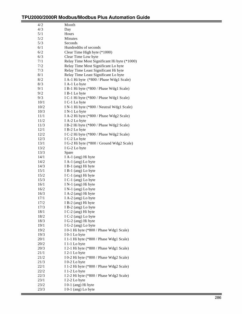
TPU2000/2000R Modbus/Modbus Plus Automation Guide
286
4/2 Month 4/3 Day 5/1 Hours 5/2 Minutes 5/3 Seconds 6/1 Hundredths of seconds 6/2 Clear Time High byte (*1000) 6/3 Clear Time Low byte 7/1 Relay Time Most Significant Hi byte (*1000) 7/2 Relay Time Most Significant Lo byte 7/3 Relay Time Least Significant Hi byte 8/1 Relay Time Least Significant Lo byte 8/2 I A-1 Hi byte (*800 / Phase Wdg1 Scale) 8/3 I A-1 Lo byte 9/1 I B-1 Hi byte (*800 / Phase Wdg1 Scale) 9/2 I B-1 Lo byte 9/3 I C-1 Hi byte (*800 / Phase Wdg1 Scale) 10/1 I C-1 Lo byte 10/2 I N-1 Hi byte (*800 / Neutral Wdg1 Scale) 10/3 I N-1 Lo byte 11/1 I A-2 Hi byte (*800 / Phase Wdg2 Scale) 11/2 I A-2 Lo byte 11/3 I B-2 Hi byte (*800 / Phase Wdg2 Scale) 12/1 I B-2 Lo byte 12/2 I C-2 Hi byte (*800 / Phase Wdg2 Scale) 12/3 I C-2 Lo byte 13/1 I G-2 Hi byte (*800 / Ground Wdg2 Scale) 13/2 I G-2 Lo byte 13/3 Spare 14/1 I A-1 (ang) Hi byte 14/2 I A-1 (ang) Lo byte 14/3 I B-1 (ang) Hi byte 15/1 I B-1 (ang) Lo byte 15/2 I C-1 (ang) Hi byte 15/3 I C-1 (ang) Lo byte 16/1 I N-1 (ang) Hi byte 16/2 I N-1 (ang) Lo byte 16/3 I A-2 (ang) Hi byte 17/1 I A-2 (ang) Lo byte 17/2 I B-2 (ang) Hi byte 17/3 I B-2 (ang) Lo byte 18/1 I C-2 (ang) Hi byte 18/2 I C-2 (ang) Lo byte 18/3 I G-2 (ang) Hi byte 19/1 I G-2 (ang) Lo byte 19/2 I 0-1 Hi byte (*800 / Phase Wdg1 Scale) 19/3 I 0-1 Lo byte 20/1 I 1-1 Hi byte (*800 / Phase Wdg1 Scale) 20/2 I 1-1 Lo byte 20/3 I 2-1 Hi byte (*800 / Phase Wdg1 Scale) 21/1 I 2-1 Lo byte 21/2 I 0-2 Hi byte (*800 / Phase Wdg2 Scale) 21/3 I 0-2 Lo byte 22/1 I 1-2 Hi byte (*800 / Phase Wdg2 Scale) 22/2 I 1-2 Lo byte 22/3 I 2-2 Hi byte (*800 / Phase Wdg2 Scale) 23/1 I 2-2 Lo byte 23/2 I 0-1 (ang) Hi byte 23/3 I 0-1 (ang) Lo byte
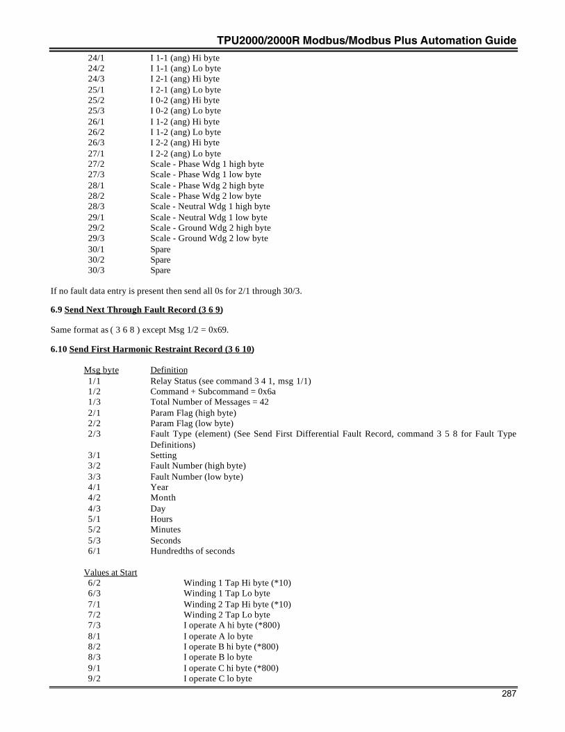
TPU2000/2000R Modbus/Modbus Plus Automation Guide
287
24/1 I 1-1 (ang) Hi byte 24/2 I 1-1 (ang) Lo byte 24/3 I 2-1 (ang) Hi byte 25/1 I 2-1 (ang) Lo byte 25/2 I 0-2 (ang) Hi byte 25/3 I 0-2 (ang) Lo byte 26/1 I 1-2 (ang) Hi byte 26/2 I 1-2 (ang) Lo byte 26/3 I 2-2 (ang) Hi byte 27/1 I 2-2 (ang) Lo byte 27/2 Scale - Phase Wdg 1 high byte 27/3 Scale - Phase Wdg 1 low byte 28/1 Scale - Phase Wdg 2 high byte 28/2 Scale - Phase Wdg 2 low byte 28/3 Scale - Neutral Wdg 1 high byte 29/1 Scale - Neutral Wdg 1 low byte 29/2 Scale - Ground Wdg 2 high byte 29/3 Scale - Ground Wdg 2 low byte 30/1 Spare 30/2 Spare 30/3 Spare
If no fault data entry is present then send all 0s for 2/1 through 30/3.
6.9 Send Next Through Fault Record (3 6 9)
Same format as ( 3 6 8 ) except Msg 1/2 = 0x69.
6.10 Send First Harmonic Restraint Record (3 6 10)
Msg byte Definition 1/1 Relay Status (see command 3 4 1, msg 1/1) 1/2 Command + Subcommand = 0x6a 1/3 Total Number of Messages = 42 2/1 Param Flag (high byte) 2/2 Param Flag (low byte) 2/3 Fault Type (element) (See Send First Differential Fault Record, command 3 5 8 for Fault Type
Definitions) 3/1 Setting 3/2 Fault Number (high byte) 3/3 Fault Number (low byte) 4/1 Year 4/2 Month 4/3 Day 5/1 Hours 5/2 Minutes 5/3 Seconds 6/1 Hundredths of seconds
Values at Start 6/2 Winding 1 Tap Hi byte (*10) 6/3 Winding 1 Tap Lo byte 7/1 Winding 2 Tap Hi byte (*10) 7/2 Winding 2 Tap Lo byte 7/3 I operate A hi byte (*800) 8/1 I operate A lo byte 8/2 I operate B hi byte (*800) 8/3 I operate B lo byte 9/1 I operate C hi byte (*800) 9/2 I operate C lo byte
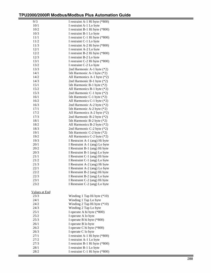
TPU2000/2000R Modbus/Modbus Plus Automation Guide
288
9/3 I restraint A-1 Hi byte (*800) 10/1 I restraint A-1 Lo byte 10/2 I restraint B-1 Hi byte (*800) 10/3 I restraint B-1 Lo byte 11/1 I restraint C-1 Hi byte (*800) 11/2 I restraint C-1 Lo byte 11/3 I restraint A-2 Hi byte (*800) 12/1 I restraint A-2 Lo byte 12/2 I restraint B-2 Hi byte (*800) 12/3 I restraint B-2 Lo byte 13/1 I restraint C-2 Hi byte (*800) 13/2 I restraint C-2 Lo byte 13/3 2nd Harmonic A-1 byte (*2) 14/1 5th Harmonic A-1 byte (*2) 14/2 All Harmonics A-1 byte (*2) 14/3 2nd Harmonic B-1 byte (*2) 15/1 5th Harmonic B-1 byte (*2) 15/2 All Harmonics B-1 byte (*2) 15/3 2nd Harmonic C-1 byte (*2) 16/1 5th Harmonic C-1 byte (*2) 16/2 All Harmonics C-1 byte (*2) 16/3 2nd Harmonic A-2 byte (*2) 17/1 5th Harmonic A-2 byte (*2) 17/2 All Harmonics A-2 byte (*2) 17/3 2nd Harmonic B-2 byte (*2) 18/1 5th Harmonic B-2 byte (*2) 18/2 All Harmonics B-2 byte (*2) 18/3 2nd Harmonic C-2 byte (*2) 19/1 5th Harmonic C-2 byte (*2) 19/2 All Harmonics C-2 byte (*2) 19/3 I Restraint A-1 (ang) Hi byte 20/1 I Restraint A-1 (ang) Lo byte 20/2 I Restraint B-1 (ang) Hi byte 20/3 I Restraint B-1 (ang) Lo byte 21/1 I Restraint C-1 (ang) Hi byte 21/2 I Restraint C-1 (ang) Lo byte 21/3 I Restraint A-2 (ang) Hi byte 22/1 I Restraint A-2 (ang) Lo byte 22/2 I Restraint B-2 (ang) Hi byte 22/3 I Restraint B-2 (ang) Lo byte 23/1 I Restraint C-2 (ang) Hi byte 23/2 I Restraint C-2 (ang) Lo byte
Values at End 23/3 Winding 1 Tap Hi byte (*10) 24/1 Winding 1 Tap Lo byte 24/2 Winding 2 Tap Hi byte (*10) 24/3 Winding 2 Tap Lo byte 25/1 I operate A hi byte (*800) 25/2 I operate A lo byte 25/3 I operate B hi byte (*800) 26/1 I operate B lo byte 26/2 I operate C hi byte (*800) 26/3 I operate C lo byte 27/1 I restraint A-1 Hi byte (*800) 27/2 I restraint A-1 Lo byte 27/3 I restraint B-1 Hi byte (*800) 28/1 I restraint B-1 Lo byte 28/2 I restraint C-1 Hi byte (*800)
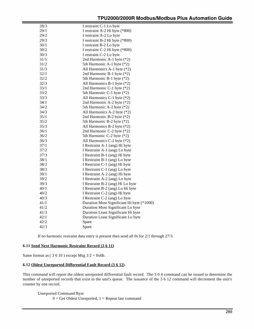
TPU2000/2000R Modbus/Modbus Plus Automation Guide
289
28/3 I restraint C-1 Lo byte 29/1 I restraint A-2 Hi byte (*800) 29/2 I restraint A-2 Lo byte 29/3 I restraint B-2 Hi byte (*800) 30/1 I restraint B-2 Lo byte 30/2 I restraint C-2 Hi byte (*800) 30/3 I restraint C-2 Lo byte 31/1 2nd Harmonic A-1 byte (*2) 31/2 5th Harmonic A-1 byte (*2) 31/3 All Harmonics A-1 byte (*2) 32/1 2nd Harmonic B-1 byte (*2) 32/2 5th Harmonic B-1 byte (*2) 32/3 All Harmonics B-1 byte (*2) 33/1 2nd Harmonic C-1 byte (*2) 33/2 5th Harmonic C-1 byte (*2) 33/3 All Harmonics C-1 byte (*2) 34/1 2nd Harmonic A-2 byte (*2) 34/2 5th Harmonic A-2 byte (*2) 34/3 All Harmonics A-2 byte (*2) 35/1 2nd Harmonic B-2 byte (*2) 35/2 5th Harmonic B-2 byte (*2) 35/3 All Harmonics B-2 byte (*2) 36/1 2nd Harmonic C-2 byte (*2) 36/2 5th Harmonic C-2 byte (*2) 36/3 All Harmonics C-2 byte (*2) 37/1 I Restraint A-1 (ang) Hi byte 37/2 I Restraint A-1 (ang) Lo byte 37/3 I Restraint B-1 (ang) Hi byte 38/1 I Restraint B-1 (ang) Lo byte 38/2 I Restraint C-1 (ang) Hi byte 38/3 I Restraint C-1 (ang) Lo byte 39/1 I Restraint A-2 (ang) Hi byte 39/2 I Restraint A-2 (ang) Lo byte 39/3 I Restraint B-2 (ang) Hi Lo byte 40/1 I Restraint B-2 (ang) Lo Hi byte 40/2 I Restraint C-2 (ang) Hi byte 40/3 I Restraint C-2 (ang) Lo byte 41/1 Duration Most Significant Hi byte (*1000) 41/2 Duration Most Significant Lo byte 41/3 Duration Least Significant Hi byte 42/1 Duration Least Significant Lo byte 42/2 Spare 42/3 Spare
If no harmonic restraint data entry is present then send all 0s for 2/1 through 27/3.
6.11 Send Next Harmonic Restraint Record (3 6 11)
Same format as ( 3 6 10 ) except Msg 1/2 = 0x6b.
6.12 Oldest Unreported Differential Fault Record (3 6 12)
This command will report the oldest unreported differential fault record. The 3 0 4 command can be issued to determine thenumber of unreported records that exist in the unit's queue. The issuance of the 3 6 12 command will decrement the unit'scounter by one record.
Unreported Command Byte0 = Get Oldest Unreported, 1 = Repeat last command
TPU2000/2000R Modbus/Modbus Plus Automation Guide
290
Data Byte Definition 1/1 Unreported Command Byte 1/2 Record Part Byte (0=Part 1, 1=Part 2) 1/3 Checksum 1/1 + 1/2
Msg Byte DefinitionSame format as (3 5 8) except Msg 1/2 = 0x6c.
6.13 Oldest Unreported Through Fault Record (3 6 13)
This command will report the oldest unreported through fault record. The 3 0 4 command can be issued to determine thenumber of unreported records that exist in the unit's queue. The issuance of the 3 6 13 command will decrement the unit'scounter by one record.
Unreported Command Byte0 = Get Oldest Unreported, 1 = Repeat last command
Data Byte Definition 1/1 Unreported Command Byte 1/2 Reserved for Differential Record Part 1/3 Checksum 1/1 + 1/2
Msg Byte DefinitionSame format as (3 6 8) except Msg 1/2 = 0x6d.
6.14 Oldest Unreported Harmonic Restraint Record (3 6 14)
This command will report the oldest unreported harmonic restraint record. The 3 0 4 command can be issued to determinethe number of unreported records that exist in the unit's queue. The issuance of the 3 6 14 command will decrement the unit'scounter by one record.
Unreported Command Byte0 = Get Oldest Unreported, 1 = Repeat last command
Data Byte Definition 1/1 Unreported Command Byte 1/2 Reserved for Differential Record Part 1/3 Checksum 1/1 + 1/2
Msg Byte DefinitionSame format as (3 6 10) except Msg 1/2 = 0x6e.
6.15 Oldest Unreported Operations Record (3 6 15)
This command will report the oldest unreported operations record. The 3 0 4 command can be issued to determine thenumber of unreported records that exist in the unit's queue. The issuance of the 3 6 15 command will decrement the unit'scounter by one record.
Unreported Command Byte0 = Get Oldest Unreported, 1 = Repeat last command
Data Byte Definition 1/1 Unreported Command Byte 1/2 Reserved for Differential Record Part 1/3 Checksum 1/1 + 1/2
Msg Byte DefinitionSame format as (3 5 12) except Msg 1/2 = 0x6f.
TPU2000/2000R Modbus/Modbus Plus Automation Guide
291
9 Trip and Energize Commands ( 3 9 n )
N Definition0 Trip Command2 Energize Output Contact Command3 Set/Reset Outputs Command
9.0 Trip Command (3 9 0)
The TRIP command will be issued to the TPU. This command has a data message that contains the Password and a commandverification code for trip.
Msg byte Definition 1/1 Most significant high byte of password 1/2 Most significant low byte of password 1/3 Least significant high byte of password 2/1 Least significant low byte of password 2/2 spare 2/3 Command + Subcommand = 0x90
9.2 Energize Output Contact Command (3 9 2)
The test output contact command will be issued to the TPU. This command has a data message that contains the Passwordand a command verification code and a 16 bit word indicating which contacts should be closed.
The output contact will be a momentary closure for the time period specified in the configuration menu for trip failure time.
Msg byte Definition 1/1 Most significant high byte of password 1/2 Most significant low byte of password 1/3 Least significant high byte of password 2/1 Least significant low byte of password 2/2 spare 2/3 Command + Subcommand = 0x92 3/1 Output Contact State
Bit 0-7 - Spare 3/2 Output Contact State
Bit 0 - TRIP Bit 1 - OUT1 Bit 2 - OUT2 Bit 3 - OUT3 Bit 4 - OUT4 Bit 5 - OUT5 Bit 6 - OUT6 Bit 7 - OUT7
3/3 Output Contact State Confirmation Bit 0-7 - Spare
4/1 Output Contact State Confirmation Bit 0 - TRIP Bit 1 - OUT1 Bit 2 - OUT2 Bit 3 - OUT3 Bit 4 - OUT4 Bit 5 - OUT5 Bit 6 - OUT6 Bit 7 - OUT7
4/2 Checksum high byte 4/3 Checksum low byte
TPU2000/2000R Modbus/Modbus Plus Automation Guide
292
9.3 Set/Reset Output Contacts Command (3 9 3)
This command allows for the assertion/deassertion of the ULO1 to ULO9 logical outputs. It also provides the means to resetthe sealed in logical output contacts. Outputs denoted with an '*' are sealed in and can only be reset.
Bit = 0, Output Not Energized/No Change in Status.Bit = 1, Output Energized/Change in Status.
Bit Output Byte1 Output Byte2 Output Byte37 87T* 150P-1* 150G-2*6 87H* 50P-2* 46-1*5 2HROA* 150P-2* 46-2*4 5HROA* 51N-1* 63*3 AHROA* 51G-2* ULO12 51P-1* 50N-1* ULO21 51P-2* 150N-1* ULO30 50P-1* 50G-2* ULO4
Bit Output Byte4 Output Bytes5-87 ULO5 SPARE6 ULO6 SPARE5 ULO7 SPARE4 ULO8 SPARE3 ULO9 SPARE2 SPARE SPARE1 SPARE SPARE0 SPARE SPARE
Example: To send a command to clear 150G-2* and set ULO4, the following command bytes should be issued.Set/Reset Output Byte3 = 01 hexStatus Change Output Byte3 = 81 hex
This allows a change to occur for outputs in bit position 7 and 0. Note that you can only clear '*' (sealed in) outputs.
Msg byte Definition 1/1 Most significant high byte of password 1/2 Most significant low byte of password 1/3 Least significant high byte of password 2/1 Least significant low byte of password 2/2 spare 2/3 Command + Subcommand = 0x93 3/1 Set/Reset Output Byte1 3/2 Set/Reset Output Byte2 3/3 Set/Reset Output Byte3 4/1 Set/Reset Output Byte4 4/2 Set/Reset Output Byte5 4/3 Set/Reset Output Byte6 5/1 Set/Reset Output Byte7 5/2 Set/Reset Output Byte8 5/3 Spare 6/1 Spare 6/2 Spare 6/3 Spare
7/1 Status Change Output Byte1 7/2 Status Change Output Byte2 7/3 Status Change Output Byte3 8/1 Status Change Output Byte4 8/2 Status Change Output Byte5 8/3 Status Change Output Byte6
TPU2000/2000R Modbus/Modbus Plus Automation Guide
293
9/1 Status Change Output Byte7 9/2 Status Change Output Byte8 9/3 Spare 10/1 Spare 10/2 Spare 10/3 Spare 11/1 Spare
11/2 Checksum high byte 11/3 Checksum low byte
10 Receive Buffer "N" Commands ( 3 10 n )
N Definition 0 Reserved for repeat 3 10 n 1 Communications Settings
10.1 Receive Communications Settings ( 3 10 1 )
Low byte consists of bits 0 through 7.High byte consists of bits 8 through 15.
Port configuration bytebit 0-3 = port baud rate (0=300,1=1200,2=2400,3=4800, 4=9600,5=19200,6=38400)bit 4-5 = parity (0=None,1=Odd,2=Even)bit 6 = number of data bits (0=seven,1=eight)bit 7 = number of stop bits (0=one,1=two)
Msg byte Definition1/1 Most significant high byte of password1/2 Most significant low byte of password1/3 Least significant high byte of password2/1 Least significant low byte of password2/2 Spare2/3 Command + Subcommand = 0xa13/1 Unit Address high byte3/2 Unit Address low byte3/3 Front Panel RS232 configuration byte4/1 Rear Panel RS232 or INCOM configuration byte4/2 Rear Panel RS485 configuration byte4/3 Rear Panel IRIG byte 0=Disabled, 1=Enabled5/1 Spare5/2 Spare5/3 Aux Port Parameter 1 byte (0-255)6/1 Aux Port Parameter 2 byte (0-255)6/2 Aux Port Parameter 3 byte (0-255)6/3 Aux Port Parameter 4 byte (0-255)7/1 Aux Port Parameter 5 byte (0-255)7/2 Aux Port Parameter 6 byte (0-255)7/3 Aux Port Parameter 7 byte (0-255)8/1 Aux Port Parameter 8 byte (0-255)8/2 Aux Port Parameter 9 byte (0-255)8/3 Aux Port Parameter 10 byte (0-255)9/1 Aux Port Parameter Mode byte9/2 Spare9/3 Spare10/1 Spare10/2 Checksum high byte10/3 Checksum low byte
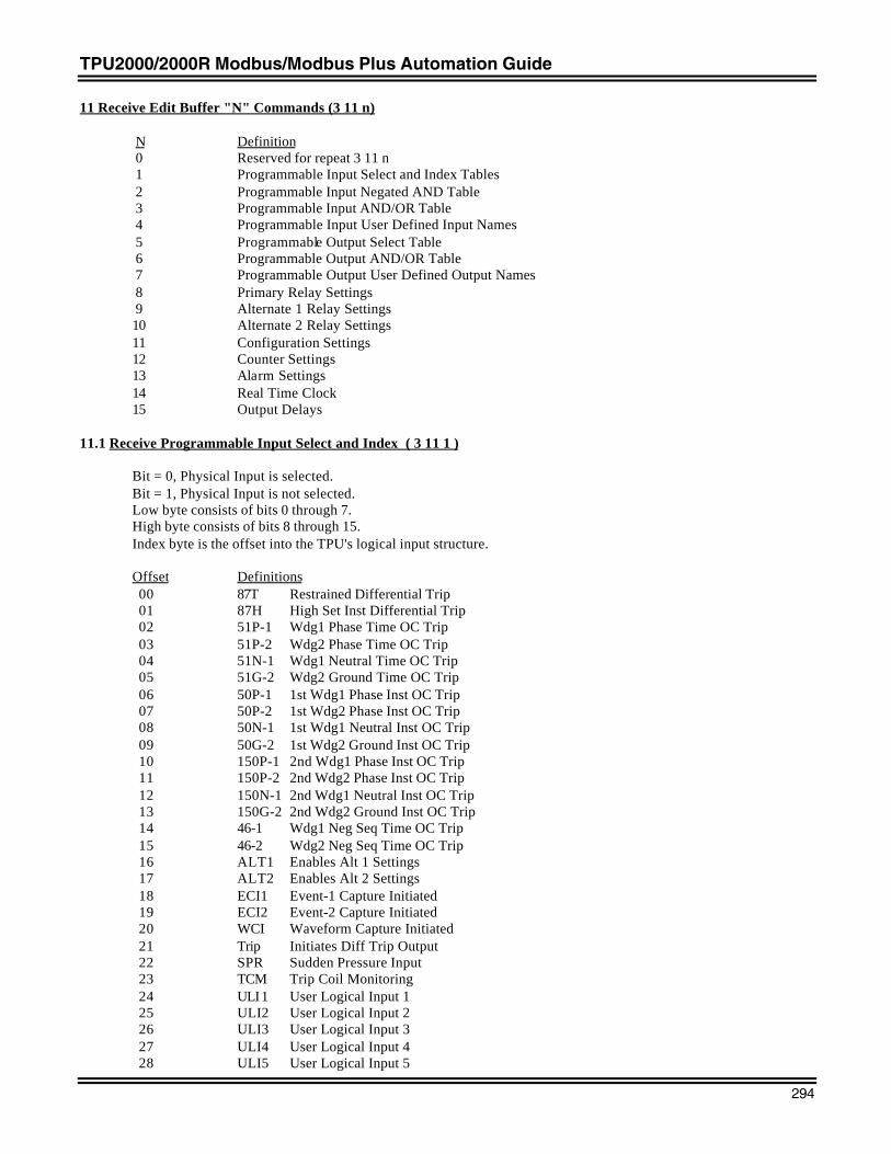
TPU2000/2000R Modbus/Modbus Plus Automation Guide
294
11 Receive Edit Buffer "N" Commands (3 11 n)
N Definition 0 Reserved for repeat 3 11 n 1 Programmable Input Select and Index Tables 2 Programmable Input Negated AND Table 3 Programmable Input AND/OR Table 4 Programmable Input User Defined Input Names 5 Programmable Output Select Table 6 Programmable Output AND/OR Table 7 Programmable Output User Defined Output Names 8 Primary Relay Settings 9 Alternate 1 Relay Settings10 Alternate 2 Relay Settings11 Configuration Settings12 Counter Settings13 Alarm Settings14 Real Time Clock15 Output Delays
11.1 Receive Programmable Input Select and Index ( 3 11 1 )
Bit = 0, Physical Input is selected.Bit = 1, Physical Input is not selected.Low byte consists of bits 0 through 7.High byte consists of bits 8 through 15.Index byte is the offset into the TPU's logical input structure.
Offset Definitions 00 87T Restrained Differential Trip 01 87H High Set Inst Differential Trip 02 51P-1 Wdg1 Phase Time OC Trip 03 51P-2 Wdg2 Phase Time OC Trip 04 51N-1 Wdg1 Neutral Time OC Trip 05 51G-2 Wdg2 Ground Time OC Trip 06 50P-1 1st Wdg1 Phase Inst OC Trip 07 50P-2 1st Wdg2 Phase Inst OC Trip 08 50N-1 1st Wdg1 Neutral Inst OC Trip 09 50G-2 1st Wdg2 Ground Inst OC Trip 10 150P-1 2nd Wdg1 Phase Inst OC Trip 11 150P-2 2nd Wdg2 Phase Inst OC Trip 12 150N-1 2nd Wdg1 Neutral Inst OC Trip 13 150G-2 2nd Wdg2 Ground Inst OC Trip 14 46-1 Wdg1 Neg Seq Time OC Trip 15 46-2 Wdg2 Neg Seq Time OC Trip 16 ALT1 Enables Alt 1 Settings 17 ALT2 Enables Alt 2 Settings 18 ECI1 Event-1 Capture Initiated 19 ECI2 Event-2 Capture Initiated 20 WCI Waveform Capture Initiated 21 Trip Initiates Diff Trip Output 22 SPR Sudden Pressure Input 23 TCM Trip Coil Monitoring 24 ULI1 User Logical Input 1 25 ULI2 User Logical Input 2 26 ULI3 User Logical Input 3 27 ULI4 User Logical Input 4 28 ULI5 User Logical Input 5
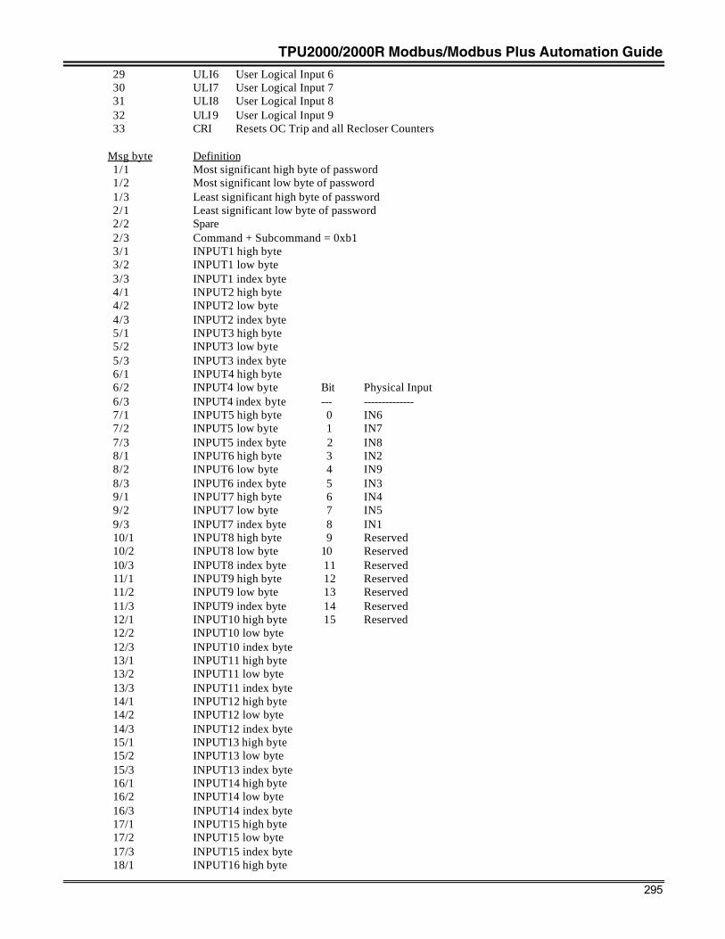
TPU2000/2000R Modbus/Modbus Plus Automation Guide
295
29 ULI6 User Logical Input 6 30 ULI7 User Logical Input 7 31 ULI8 User Logical Input 8 32 ULI9 User Logical Input 9 33 CRI Resets OC Trip and all Recloser Counters
Msg byte Definition 1/1 Most significant high byte of password 1/2 Most significant low byte of password 1/3 Least significant high byte of password 2/1 Least significant low byte of password 2/2 Spare 2/3 Command + Subcommand = 0xb1 3/1 INPUT1 high byte 3/2 INPUT1 low byte 3/3 INPUT1 index byte 4/1 INPUT2 high byte 4/2 INPUT2 low byte 4/3 INPUT2 index byte 5/1 INPUT3 high byte 5/2 INPUT3 low byte 5/3 INPUT3 index byte 6/1 INPUT4 high byte 6/2 INPUT4 low byte Bit Physical Input 6/3 INPUT4 index byte --- -------------- 7/1 INPUT5 high byte 0 IN6 7/2 INPUT5 low byte 1 IN7 7/3 INPUT5 index byte 2 IN8 8/1 INPUT6 high byte 3 IN2 8/2 INPUT6 low byte 4 IN9 8/3 INPUT6 index byte 5 IN3 9/1 INPUT7 high byte 6 IN4 9/2 INPUT7 low byte 7 IN5 9/3 INPUT7 index byte 8 IN1 10/1 INPUT8 high byte 9 Reserved 10/2 INPUT8 low byte 10 Reserved 10/3 INPUT8 index byte 11 Reserved 11/1 INPUT9 high byte 12 Reserved 11/2 INPUT9 low byte 13 Reserved 11/3 INPUT9 index byte 14 Reserved 12/1 INPUT10 high byte 15 Reserved 12/2 INPUT10 low byte 12/3 INPUT10 index byte 13/1 INPUT11 high byte 13/2 INPUT11 low byte 13/3 INPUT11 index byte 14/1 INPUT12 high byte 14/2 INPUT12 low byte 14/3 INPUT12 index byte 15/1 INPUT13 high byte 15/2 INPUT13 low byte 15/3 INPUT13 index byte 16/1 INPUT14 high byte 16/2 INPUT14 low byte 16/3 INPUT14 index byte 17/1 INPUT15 high byte 17/2 INPUT15 low byte 17/3 INPUT15 index byte 18/1 INPUT16 high byte
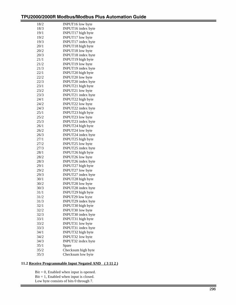
TPU2000/2000R Modbus/Modbus Plus Automation Guide
296
18/2 INPUT16 low byte 18/3 INPUT16 index byte 19/1 INPUT17 high byte 19/2 INPUT17 low byte 19/3 INPUT17 index byte 20/1 INPUT18 high byte 20/2 INPUT18 low byte 20/3 INPUT18 index byte 21/1 INPUT19 high byte 21/2 INPUT19 low byte 21/3 INPUT19 index byte 22/1 INPUT20 high byte 22/2 INPUT20 low byte 22/3 INPUT20 index byte 23/1 INPUT21 high byte 23/2 INPUT21 low byte 23/3 INPUT21 index byte 24/1 INPUT22 high byte 24/2 INPUT22 low byte 24/3 INPUT22 index byte 25/1 INPUT23 high byte 25/2 INPUT23 low byte 25/3 INPUT23 index byte 26/1 INPUT24 high byte 26/2 INPUT24 low byte 26/3 INPUT24 index byte 27/1 INPUT25 high byte 27/2 INPUT25 low byte 27/3 INPUT25 index byte 28/1 INPUT26 high byte 28/2 INPUT26 low byte 28/3 INPUT26 index byte 29/1 INPUT27 high byte 29/2 INPUT27 low byte 29/3 INPUT27 index byte 30/1 INPUT28 high byte 30/2 INPUT28 low byte 30/3 INPUT28 index byte 31/1 INPUT29 high byte 31/2 INPUT29 low byte 31/3 INPUT29 index byte 32/1 INPUT30 high byte 32/2 INPUT30 low byte 32/3 INPUT30 index byte 33/1 INPUT31 high byte 33/2 INPUT31 low byte 33/3 INPUT31 index byte 34/1 INPUT32 high byte 34/2 INPUT32 low byte 34/3 INPUT32 index byte 35/1 Spare 35/2 Checksum high byte 35/3 Checksum low byte
11.2 Receive Programmable Input Negated AND ( 3 11 2 )
Bit = 0, Enabled when input is opened.Bit = 1, Enabled when input is closed.Low byte consists of bits 0 through 7.
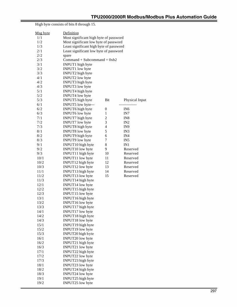
TPU2000/2000R Modbus/Modbus Plus Automation Guide
297
High byte consists of bits 8 through 15.
Msg byte Definition 1/1 Most significant high byte of password 1/2 Most significant low byte of password 1/3 Least significant high byte of password 2/1 Least significant low byte of password 2/2 spare 2/3 Command + Subcommand = 0xb2 3/1 INPUT1 high byte 3/2 INPUT1 low byte 3/3 INPUT2 high byte 4/1 INPUT2 low byte 4/2 INPUT3 high byte 4/3 INPUT3 low byte 5/1 INPUT4 high byte 5/2 INPUT4 low byte 5/3 INPUT5 high byte Bit Physical Input 6/1 INPUT5 low byte--- -------------- 6/2 INPUT6 high byte 0 IN6 6/3 INPUT6 low byte 1 IN7 7/1 INPUT7 high byte 2 IN8 7/2 INPUT7 low byte 3 IN2 7/3 INPUT8 high byte 4 IN9 8/1 INPUT8 low byte 5 IN3 8/2 INPUT9 high byte 6 IN4 8/3 INPUT9 low byte 7 IN5 9/1 INPUT10 high byte 8 IN1 9/2 INPUT10 low byte 9 Reserved 9/3 INPUT11 high byte 10 Reserved 10/1 INPUT11 low byte 11 Reserved 10/2 INPUT12 high byte 12 Reserved 10/3 INPUT12 low byte 13 Reserved 11/1 INPUT13 high byte 14 Reserved 11/2 INPUT13 low byte 15 Reserved 11/3 INPUT14 high byte 12/1 INPUT14 low byte 12/2 INPUT15 high byte 12/3 INPUT15 low byte 13/1 INPUT16 high byte 13/2 INPUT16 low byte 13/3 INPUT17 high byte 14/1 INPUT17 low byte 14/2 INPUT18 high byte 14/3 INPUT18 low byte 15/1 INPUT19 high byte 15/2 INPUT19 low byte 15/3 INPUT20 high byte 16/1 INPUT20 low byte 16/2 INPUT21 high byte 16/3 INPUT21 low byte 17/1 INPUT22 high byte 17/2 INPUT22 low byte 17/3 INPUT23 high byte 18/1 INPUT23 low byte 18/2 INPUT24 high byte 18/3 INPUT24 low byte 19/1 INPUT25 high byte 19/2 INPUT25 low byte
TPU2000/2000R Modbus/Modbus Plus Automation Guide
298
19/3 INPUT26 high byte 20/1 INPUT26 low byte 20/2 INPUT27 high byte 20/3 INPUT27 low byte 21/1 INPUT28 high byte 21/2 INPUT28 low byte 21/3 INPUT29 high byte 22/1 INPUT29 low byte 22/2 INPUT30 high byte 22/3 INPUT30 low byte 23/1 INPUT31 high byte 23/2 INPUT31 low byte 23/3 INPUT32 high byte 24/1 INPUT32 low byte 24/2 Checksum high byte 24/3 Checksum low byte
11.3 Receive Programmable Input AND/OR Select ( 3 11 3 )
Bit = 0, Selected inputs are ORed together.Bit = 1, Selected inputs are ANDed together.
Msg byte Definition 1/1 Most significant high byte of password 1/2 Most significant low byte of password 1/3 Least significant high byte of password 2/1 Least significant low byte of password 2/2 spare 2/3 Command + Subcommand = 0xb3 3/1 Programmable input AND/OR selection bits 24-31 3/2 Programmable input AND/OR selection bits 16-23 3/3 Programmable input AND/OR selection bits 8-15 4/1 Programmable input AND/OR selection bits 0-7 4/2 Checksum high byte 4/3 Checksum low byte
Bit Logical Input --- ------------ 0 INPUT1 1 INPUT2 . . . 27 INPUT28 28 INPUT29 29 INPUT30 30 INPUT31 31 INPUT32
11.4 Receive Programmable Input User Defined Strings ( 3 11 4 )
User definable 8 char input strings. Byte 9 is an implied NULL
Msg byte Definition1/1 Most significant high byte of password1/2 Most significant low byte of password1/3 Least significant high byte of password2/1 Least significant low byte of password2/2 spare
TPU2000/2000R Modbus/Modbus Plus Automation Guide
299
2/3 Command + Subcommand = 0xb43/1-5/2 IN1 Character String 8 bytes5/3-8/1 IN2 Character String 8 bytes8/2-10/3 IN3 Character String 8 bytes11/1-13/2 IN4 Character String 8 bytes13/3-16/1 IN5 Character String 8 bytes16/2-18/3 IN6 Character String 8 bytes19/1-21/2 IN7 Character String 8 bytes21/3-24/1 IN8 Character String 8 bytes24/2-26/3 IN9 Character String 8 bytes27/1-29/2 spare Character String 8 bytes29/3-32/1 spare Character String 8 bytes32/2-34/3 spare Character String 8 bytes35/1-37/2 spare Character String 8 bytes37/3-38/1 spares38/2 Checksum high byte38/3 Checksum low byte
11.5 Receive Programmable Output Select ( 3 11 5 )
Programmable Output data transferred from PC to TPU2000.
Bit = 0, Physical Output is selected.Bit = 1, Physical Output is not selected.Least significant low byte consists of bits 0 through 7.Least significant high byte consists of bits 8 through 15.Most significant low byte consists of bits 16 through 23.Most significant high byte consists of bits 24 through 31.
Msg byte Definition 1/1 Most significant high byte of password 1/2 Most significant low byte of password 1/3 Least significant high byte of password 2/1 Least significant low byte of password 2/2 spare 2/3 Command + Subcommand = 0xb5 3/1 Contact OUT5 most significant high byte 3/2 Contact OUT5 most significant low byte 3/3 Contact OUT5 least significant high byte 4/1 Contact OUT5 least significant low byte 4/2 Contact OUT7 most significant high byte 4/3 Contact OUT7 most significant low byte 5/1 Contact OUT7 least significant high byte 5/2 Contact OUT7 least significant low byte 5/3 Contact OUT4 most significant high byte 6/1 Contact OUT4 most significant low byte 6/2 Contact OUT4 least significant high byte 6/3 Contact OUT4 least significant low byte 7/1 Contact OUT6 most significant high byte 7/2 Contact OUT6 most significant low byte 7/3 Contact OUT6 least significant high byte 8/1 Contact OUT6 least significant low byte 8/2 Contact OUT3 most significant high byte 8/3 Contact OUT3 most significant low byte 9/1 Contact OUT3 least significant high byte 9/2 Contact OUT3 least significant low byte 9/3 Contact OUT2 most significant high byte 10/1 Contact OUT2 most significant low byte 10/2 Contact OUT2 least significant high byte
TPU2000/2000R Modbus/Modbus Plus Automation Guide
300
10/3 Contact OUT2 least significant low byte 11/1 Contact OUT1 most significant high byte 11/2 Contact OUT1 most significant low byte 11/3 Contact OUT1 least significant high byte 12/1 Contact OUT1 least significant low byte 12/2-22/1 spare 22/2 Checksum high byte 22/3 Checksum low byte
Bit Logical Output --- -------------- 0 TRIP 1 OUTPUT1 2 OUTPUT2 3 OUTPUT3 . . . 30 OUTPUT29 31 OUTPUT30
11.6 Receive Programmable Output AND/OR Index ( 3 11 6 )
Bit = 0, Selected outputs are ORed together.Bit = 1, Selected outputs are ANDed together.Index byte is the offset into the TPU's logical output structure.
Index Output Definition00 DIFF Fixed Diff Trip, 87T or 87H01 ALARM Fixed Self Check Alarm02 87T Percentage Differential Trip03 87H High Set Inst Diff Trip04 2HROA 2nd Harm Restraint Output Alarm05 5HROA 5th Harm Restraint Alarm06 AHROA All Harm Restraint Alarm07 TCFA Trip Circuit Failure Alarm08 TFA Trip Failure Alarm09 51P-1 Wdg 1 Phase Time OC Trip10 51P-2 Wdg 2 Phase Time OC Trip11 50P-1 1st Wdg 1 Phase Inst OC Trip12 150P-1 2nd Wdg 1 Phase Inst OC Trip13 50P-2 1st Wdg 2 Phase Inst OC Trip14 150P-2 2nd Wdg 2 Phase Inst OC Trip15 51N-1 Wdg 1 Neutral Time OC Trip16 51G-2 Wdg 2 Ground Time OC Trip17 50N-1 1st Wdg 1 Neutral Inst OC Trip18 150N-1 2nd Wdg 1 Neutral Inst OC Trip19 50G-2 1st Wdg 2 Ground Inst OC Trip20 150G-2 2nd Wdg 2 Ground Inst OC Trip21 46-1 Wdg 1 Neg Sequence Time OC Trip22 46-2 Wdg 2 Neg Sequence Time OC Trip23 87T-D Percentage Differential Disabled Alarm24 87H-D High Set Inst Diff Disabled Alarm25 51P-1D Wdg 1 Phase Time OC Disabled Alarm26 51P-2D Wdg 2 Phase Time OC Disabled Alarm27 51N-1D Wdg 1 Neutral Time OC Disabled Alarm28 51G-2D Wdg 2 Ground Time OC Disabled Alarm29 50P-1D 1st Wdg 1 Phase Inst OC Disabled Alarm30 50P-2D 1st Wdg 2 Phase Inst OC Disabled Alarm
TPU2000/2000R Modbus/Modbus Plus Automation Guide
301
31 50N-1D 1st Wdg 1 Neutral Inst OC Disabled Alarm32 50G-2D 1st Wdg 2 Ground Inst OC Disabled Alarm33 150P-1D 2nd Wdg 1 Phase Inst Disabled Alarm34 150P-2D 2nd Wdg 2 Phase Inst Disabled Alarm35 150N-1D 2nd Wdg 1 Neutral Inst Disabled Alarm36 150G-2D 2nd Wdg 2 Ground Inst Disabled Alarm37 46-1D Wdg 1 Neg Seq Time OC Disabled Alarm38 46-2D Wdg 2 Neg Seq Time OC Disabled Alarm39 PATA Phase A LED Alarm40 PBTA Phase B LED Alarm41 PCTA Phase C LED Alarm42 PUA Pickup Alarm43 63 Sudden Pressure Input Alarm44 THRUFA Through Fault Alarm45 TFCA Through Fault Counter Alarm46 TFKA Through Fault KAmp Summation Alarm47 TFSCA Through Fault Cycle Summation Alarm48 DTC Differential Trip Counter Alarm49 OCTC Overcurrent Trip Counter Alarm50 PDA Phase Current Demand Alarm51 NDA Neutral Current Demand Alarm52 PRIM Primary Set Enabled Alarm53 ALT1 Alt1 Set Enabled Alarm54 ALT2 Alt2 Set Enabled Alarm55 STCA Settings Table Changed Alarm56 87T* Percentage Diff Sealed In Alarm57 87H* High Set Inst Diff Sealed In Alarm58 2HROA* 2nd Harmonic Restraint Sealed In Alarm59 5HROA* 5th Harmonic Restraint Sealed In Alarm60 AHROA* All Harmonic Restraint Sealed In Alarm61 51P-1* Wdg 1 Phase Time OC Sealed In Alarm62 51P-2* Wdg 2 Phase Time OC Sealed In Alarm63 50P-1* 1st Wdg1 Phase Inst OC Sealed In Alarm64 150P-1* 2nd Wdg1 Phase Inst OC Sealed In Alarm65 50P-2* 1st Wdg2 Phase Inst OC Sealed In Alarm66 150P-2* 2nd Wdg2 Phase Inst OC Sealed In Alarm67 51N-1* Wdg1 Neutral Time OC Sealed In Alarm68 51G-2* Wdg2 Ground Time OC Sealed In Alarm69 50N-1* 1st Wdg1 Neutral Inst OC Sealed In Alarm70 150N-1* 2nd Wdg1 Neutral Inst OC Sealed In Alarm71 50G-2* 1st Wdg2 Ground Inst OC Sealed In Alarm72 150G-2* 2nd Wdg2 Ground Inst OC Sealed In Alarm73 46-1* Wdg1 Neg Seq Time OC Sealed In Alarm74 46-2* Wdg2 Neg Seq Time OC Sealed In Alarm75 63* Sudden Pressure Input Sealed In Alarm76 ULO1 User Logical Output 177 ULO2 User Logical Output 278 ULO3 User Logical Output 379 ULO4 User Logical Output 480 ULO5 User Logical Output 581 ULO6 User Logical Output 682 ULO7 User Logical Output 783 ULO8 User Logical Output 884 ULO9 User Logical Output 985 LOADA Load Current86 OCA-1 Overcurrent Alarm Winding 187 OCA-2 Overcurrent Alarm Winding 288 HLDA-1 High Level Detection Alarm Winding 189 LLDA-1 Low Level Detection Alarm Winding 1
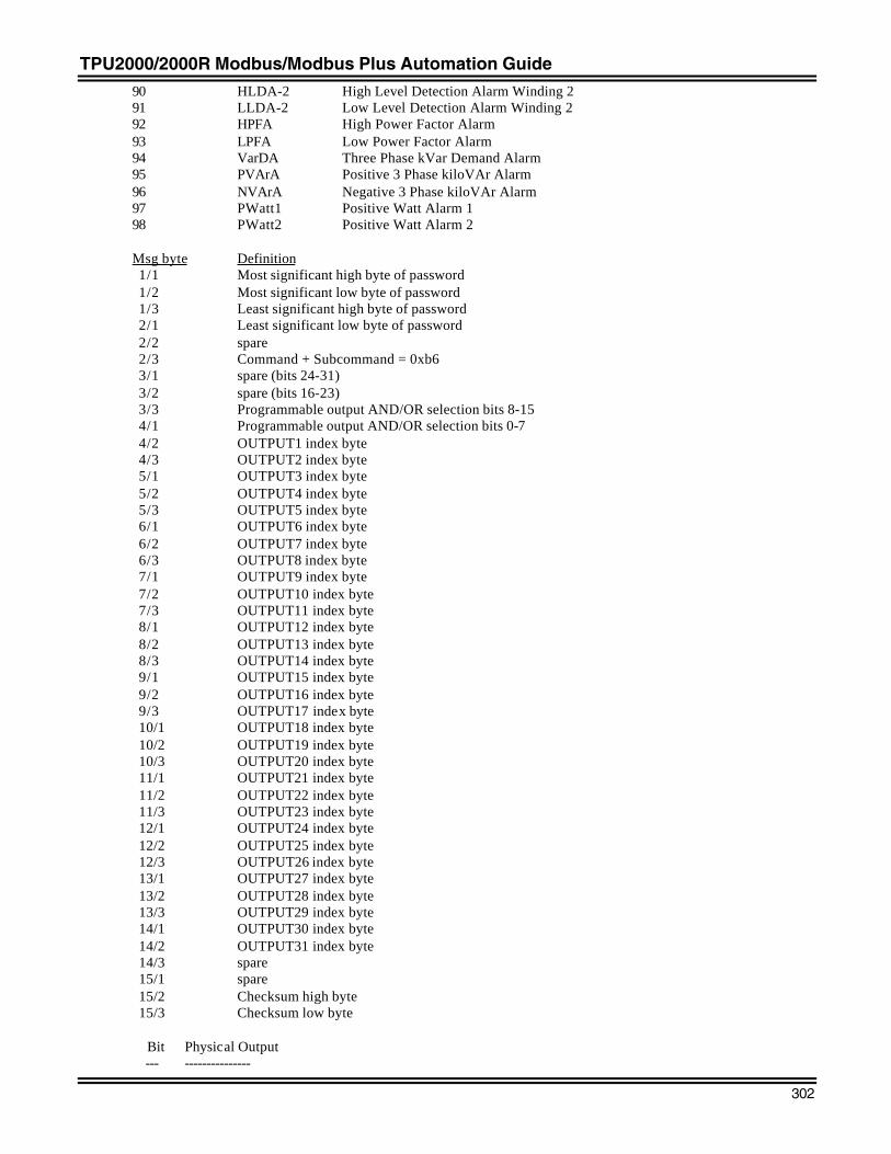
TPU2000/2000R Modbus/Modbus Plus Automation Guide
302
90 HLDA-2 High Level Detection Alarm Winding 291 LLDA-2 Low Level Detection Alarm Winding 292 HPFA High Power Factor Alarm93 LPFA Low Power Factor Alarm94 VarDA Three Phase kVar Demand Alarm95 PVArA Positive 3 Phase kiloVAr Alarm96 NVArA Negative 3 Phase kiloVAr Alarm97 PWatt1 Positive Watt Alarm 198 PWatt2 Positive Watt Alarm 2
Msg byte Definition 1/1 Most significant high byte of password 1/2 Most significant low byte of password 1/3 Least significant high byte of password 2/1 Least significant low byte of password 2/2 spare 2/3 Command + Subcommand = 0xb6 3/1 spare (bits 24-31) 3/2 spare (bits 16-23) 3/3 Programmable output AND/OR selection bits 8-15 4/1 Programmable output AND/OR selection bits 0-7 4/2 OUTPUT1 index byte 4/3 OUTPUT2 index byte 5/1 OUTPUT3 index byte 5/2 OUTPUT4 index byte 5/3 OUTPUT5 index byte 6/1 OUTPUT6 index byte 6/2 OUTPUT7 index byte 6/3 OUTPUT8 index byte 7/1 OUTPUT9 index byte 7/2 OUTPUT10 index byte 7/3 OUTPUT11 index byte 8/1 OUTPUT12 index byte 8/2 OUTPUT13 index byte 8/3 OUTPUT14 index byte 9/1 OUTPUT15 index byte 9/2 OUTPUT16 index byte 9/3 OUTPUT17 index byte 10/1 OUTPUT18 index byte 10/2 OUTPUT19 index byte 10/3 OUTPUT20 index byte 11/1 OUTPUT21 index byte 11/2 OUTPUT22 index byte 11/3 OUTPUT23 index byte 12/1 OUTPUT24 index byte 12/2 OUTPUT25 index byte 12/3 OUTPUT26 index byte 13/1 OUTPUT27 index byte 13/2 OUTPUT28 index byte 13/3 OUTPUT29 index byte 14/1 OUTPUT30 index byte 14/2 OUTPUT31 index byte 14/3 spare 15/1 spare 15/2 Checksum high byte 15/3 Checksum low byte
Bit Physical Output --- ---------------
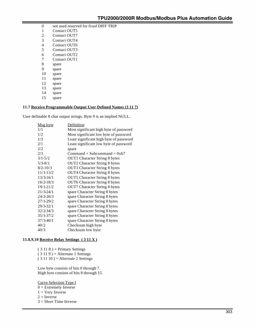
TPU2000/2000R Modbus/Modbus Plus Automation Guide
303
0 not used reserved for fixed DIFF TRIP 1 Contact OUT5 2 Contact OUT7 3 Contact OUT4 4 Contact OUT6 5 Contact OUT3 6 Contact OUT2 7 Contact OUT1 8 spare 9 spare 10 spare 11 spare 12 spare 13 spare 14 spare 15 spare
11.7 Receive Programmable Output User Defined Names (3 11 7)
User definable 8 char output strings. Byte 9 is an implied NULL.
Msg byte Definition1/1 Most significant high byte of password1/2 Most significant low byte of password1/3 Least significant high byte of password2/1 Least significant low byte of password2/2 spare2/3 Command + Subcommand = 0xb73/1-5/2 OUT1 Character String 8 bytes5/3-8/1 OUT2 Character String 8 bytes8/2-10/3 OUT3 Character String 8 bytes11/1-13/2 OUT4 Character String 8 bytes13/3-16/1 OUT5 Character String 8 bytes16/2-18/3 OUT6 Character String 8 bytes19/1-21/2 OUT7 Character String 8 bytes21/3-24/1 spare Character String 8 bytes24/2-26/3 spare Character String 8 bytes27/1-29/2 spare Character String 8 bytes29/3-32/1 spare Character String 8 bytes32/2-34/3 spare Character String 8 bytes35/1-37/2 spare Character String 8 bytes37/3-40/1 spare Character String 8 bytes40/2 Checksum high byte40/3 Checksum low byte
11.8,9,10 Receive Relay Settings ( 3 11 X )
( 3 11 8 ) = Primary Settings( 3 11 9 ) = Alternate 1 Settings( 3 11 10 ) = Alternate 2 Settings
Low byte consists of bits 0 through 7.High byte consists of bits 8 through 15.
Curve Selection Type I0 = Extremely Inverse1 = Very Inverse2 = Inverse3 = Short Time Inverse
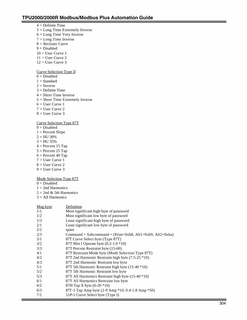
TPU2000/2000R Modbus/Modbus Plus Automation Guide
304
4 = Definite Time5 = Long Time Extremely Inverse6 = Long Time Very Inverse7 = Long Time Inverse8 = Recloser Curve9 = Disabled10 = User Curve 111 = User Curve 212 = User Curve 3
Curve Selection Type II0 = Disabled1 = Standard2 = Inverse3 = Definite Time4 = Short Time Inverse5 = Short Time Extremely Inverse6 = User Curve 17 = User Curve 28 = User Curve 3
Curve Selection Type 87T0 = Disabled1 = Percent Slope2 = HU 30%3 = HU 35%4 = Percent 15 Tap5 = Percent 25 Tap6 = Percent 40 Tap7 = User Curve 18 = User Curve 29 = User Curve 3
Mode Selection Type 87T0 = Disabled1 = 2nd Harmonics2 = 2nd & 5th Harmonics3 = All Harmonics
Msg byte Definition1/1 Most significant high byte of password1/2 Most significant low byte of password1/3 Least significant high byte of password2/1 Least significant low byte of password2/2 spare2/3 Command + Subcommand = (Prim=0xb8, Alt1=0xb9, Alt2=0xba)3/1 87T Curve Select byte (Type 87T)3/2 87T Min I Operate byte (0.2-1.0 *10)3/3 87T Percent Restraint byte (15-60)4/1 87T Restraint Mode byte (Mode Selection Type 87T)4/2 87T 2nd Harmonic Restraint high byte (7.5-25 *10)4/3 87T 2nd Harmonic Restraint low byte5/1 87T 5th Harmonic Restraint high byte (15-40 *10)5/2 87T 5th Harmonic Restraint low byte5/3 87T All Harmonics Restraint high byte (15-40 *10)6/1 87T All Harmonics Restraint low byte6/2 87H Tap X byte (6-20 *10)6/3 87T-1 Tap Amp byte (2-9 Amp *10, 0.4-1.8 Amp *50)7/1 51P-1 Curve Select byte (Type I)
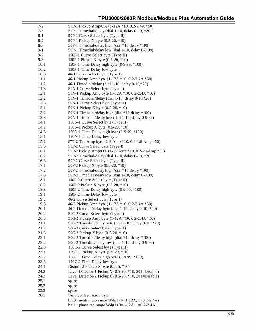
TPU2000/2000R Modbus/Modbus Plus Automation Guide
305
7/2 51P-1 Pickup Amp/OA (1-12A *10, 0.2-2.4A *50)7/3 51P-1 Timedial/delay (dial 1-10, delay 0-10, *20)8/1 50P-1 Curve Select byte (Type II)8/2 50P-1 Pickup X byte (0.5-20, *10)8/3 50P-1 Timedial/delay high (dial *10,delay *100)9/1 50P-1 Timedial/delay low (dial 1-10, delay 0-9.99)9/2 150P-1 Curve Select byte (Type II)9/3 150P-1 Pickup X byte (0.5-20, *10)10/1 150P-1 Time Delay high byte (0-9.99, *100)10/2 150P-1 Time Delay low byte10/3 46-1 Curve Select byte (Type I)11/1 46-1 Pickup Amp byte (1-12A *10, 0.2-2.4A *50)11/2 46-1 Timedial/delay (dial 1-10, delay 0-10,*20)11/3 51N-1 Curve Select byte (Type I)12/1 51N-1 Pickup Amp byte (1-12A *10, 0.2-2.4A *50)12/2 51N-1 Timedial/delay (dial 1-10, delay 0-10,*20)12/3 50N-1 Curve Select byte (Type II)13/1 50N-1 Pickup X byte (0.5-20, *10)13/2 50N-1 Timedial/delay high (dial *10,delay *100)13/3 50N-1 Timedial/delay low (dial 1-10, delay 0-9.99)14/1 150N-1 Curve Select byte (Type II)14/2 150N-1 Pickup X byte (0.5-20, *10)14/3 150N-1 Time Delay high byte (0-9.99, *100)15/1 150N-1 Time Delay low byte15/2 87T-2 Tap Amp byte (2-9 Amp *10, 0.4-1.8 Amp *50)15/3 51P-2 Curve Select byte (Type I)16/1 51P-2 Pickup Amp/OA (1-12 Amp *10, 0.2-2.4Amp *50)16/2 51P-2 Timedial/delay (dial 1-10, delay 0-10, *20)16/3 50P-2 Curve Select byte (Type II)17/1 50P-2 Pickup X byte (0.5-20, *10)17/2 50P-2 Timedial/delay high (dial *10,delay *100)17/3 50P-2 Timedial/delay low (dial 1-10, delay 0-9.99)18/1 150P-2 Curve Select byte (Type II)18/2 150P-2 Pickup X byte (0.5-20, *10)18/3 150P-2 Time Delay high byte (0-9.99, *100)19/1 150P-2 Time Delay low byte19/2 46-2 Curve Select byte (Type I)19/3 46-2 Pickup Amp byte (1-12A *10, 0.2-2.4A *50)20/1 46-2 Timedial/delay byte (dial 1-10, delay 0-10, *20)20/2 51G-2 Curve Select byte (Type I)20/3 51G-2 Pickup Amp byte (1-12A *10, 0.2-2.4A *50)21/1 51G-2 Timedial/delay byte (dial 1-10, delay 0-10, *20)21/2 50G-2 Curve Select byte (Type II)21/3 50G-2 Pickup X byte (0.5-20, *10)22/1 50G-2 Timedial/delay high (dial *10,delay *100)22/2 50G-2 Timedial/delay low (dial 1-10, delay 0-9.99)22/3 150G-2 Curve Select byte (Type II)23/1 150G-2 Pickup X byte (0.5-20, *10)23/2 150G-2 Time Delay high byte (0-9.99, *100)23/3 150G-2 Time Delay low byte24/1 Disturb-2 Pickup X byte (0.5-5, *10)24/2 Level Detector-1 PickupX (0.5-20, *10, 201=Disable)24/3 Level Detector-2 PickupX (0.5-20, *10, 201=Disable)25/1 spare25/2 spare25/3 spare26/1 Unit Configuration byte
bit 0 : neutral tap range Wdg1 (0=1-12A, 1=0.2-2.4A)bit 1 : phase tap range Wdg1 (0=1-12A, 1=0.2-2.4A)
TPU2000/2000R Modbus/Modbus Plus Automation Guide
306
bit 2 : neutral tap range Wdg2 (0=1-12A, 1=0.2-2.4A)bit 3 : phase tap range Wdg2 (0=1-12A, 1=0.2-2.4A)bit 4 : user definable curvesbit 5 : Reserved for frequencybit 6 : neutral tap range Wdg3 (0=1-12A, 1=0.2-2.4A)bit 7 : phase tap range Wdg3 (0=1-12A, 1=0.2-2.4A)
26/2 Checksum high byte26/3 Checksum low byte
11.11 Receive Configuration Settings ( 3 11 11 )
Low byte consists of bits 0 through 7.High byte consists of bits 8 through 15.
Mode Selection Type Trip Failure0 = Differential Trip1 = OC Alarm2 = Differential and OC Alarm
Mode Selection Type Demand Time Constant0 = 51 = 152 = 303 = 60
Msg byte Definition 1/1 Most significant high byte of password 1/2 Most significant low byte of password 1/3 Least significant high byte of password 2/1 Least significant low byte of password 2/2 spare 2/3 Command + Subcommand = 0xbb 3/1 Wdg1 P CT Ratio high byte (1-2000) 3/2 Wdg1 P CT Ratio low byte 3/3 Wdg1 N CT Ratio high byte (1-2000) 4/1 Wdg1 N CT Ratio low byte 4/2 Wdg2 P CT Ratio high byte (1-2000) 4/3 Wdg2 P CT Ratio low byte 5/1 Wdg2 G CT Ratio high byte (1-2000) 5/2 Wdg2 G CT Ratio low byte 5/3 Winding Phase Comp high byte (0-330, /30) 6/1 Winding Phase Comp low byte 6/2 Wind1 CT Config high byte (0=Wye; 1=Delta, IA-IC; 2=Delta, IA-IB) 6/3 Wind1 CT Config low byte 7/1 Wind2 CT Config h igh byte (0=Wye; 1=Delta, IA-IC; 2=Delta, IA-IB) 7/2 Wind2 CT Config low byte 7/3 Phase Rotation high byte (0=ABC, 1=ACB) 8/1 Phase Rotation low byte 8/2 Alt 1 Settings high byte (0=Disable, 1=Enable) 8/3 Alt 1 Settings low byte 9/1 Alt 2 Settings high byte (0=Disable, 1=Enable) 9/2 Alt 2 Settings low byte 9/3 Trip Failure Mode high byte (Type Trip Failure) 10/1 Trip Failure Mode low byte 10/2 Trip Failure Time high byte (5-60) 10/3 Trip Failure Time low byte 11/1 Trip Fail Dropout % PU high byte (5-90) 11/2 Trip Fail Dropout % PU low byte 11/3 Configuration Flag high byte
TPU2000/2000R Modbus/Modbus Plus Automation Guide
307
bit 8 : Cross Block Mode (0=Disable, 1=Enable)bit 9 : SPAREbit 10 : SPAREbit 11 : SPAREbit 12 : SPAREbit 13 : SPAREbit 14 : SPAREbit 15 : SPARE
12/1 Configuration Flag low bytebit 0 : OC Protect Mode (0=Fund, 1=RMS)bit 1 : Reset Mode (0=Instant 1=Delayed)bit 2 : Sparebit 3 : Target Display Mode (0=Last, 1=All)bit 4 : Local Edit (0=Disable, 1=Enable)bit 5 : Remote Edit (0=Disable, 1=Enable)bit 6 : WHr/VARHr Meter Mode (0=KWHr, 1=MWHr)bit 7 : LCD Light (0=Timer, 1=On)
12/2 Unit Name character 1 12/3 Unit Name character 2 13/1 Unit Name character 3 13/2 Unit Name character 4 13/3 Unit Name character 5 14/1 Unit Name character 6 14/2 Unit Name character 7 14/3 Unit Name character 8 15/1 Unit Name character 9 15/2 Unit Name character 10 15/3 Unit Name character 11 16/1 Unit Name character 12 16/2 Unit Name character 13 16/3 Unit Name character 14 17/1 Unit Name character 15 17/2 Transformer Configuration Byte (0=Wye1-Wye2, 1=Wye1-Delta2, 2=Delta1-Wye2, 3=Delta1-Delta2) 17/3 Demand Time Const high byte (Type Demand Time) 18/1 Demand Time Const low byte 18/2 LCD Contrast Adjustment high byte (0-63) 18/3 LCD Contrast Adjustment low byte 19/1 Relay Password character 1 19/2 Relay Password character 2 19/3 Relay Password character 3 20/1 Relay Password character 4 20/2 Meter Winding Mode (0=Wdg1, 1=Wdg2, 2=Wdg3) 20/3 VT Configuration (0=69VWye, 1=120VWye, 2=120V Delta, 3=208V Delta)
21/1 VT Ratio high byte (1-2000) 21/2 VT Ratio low byte 21/3 spare 22/1 spare 22/2 Checksum high byte 22/3 Checksum low byte
11.12 Receive Counter Settings ( 3 11 12 )
Low byte consists of bits 0 through 7.High byte consists of bits 8 through 15.
Msg byte Definition 1/1 Most significant high byte of password 1/2 Most significant low byte of password 1/3 Least significant high byte of password
TPU2000/2000R Modbus/Modbus Plus Automation Guide
308
2/1 Least significant low byte of password 2/2 spare 2/3 Command + Subcommand = 0xbc 3/1 Through Faults Counter high byte (0-9999) 3/2 Through Faults Counter low byte 3/3 Thr Fault Sum kAmp A Counter high byte (0-9999) 4/1 Thr Fault Sum kAmp A Counter low byte 4/2 Through Fault Sum Cyc Counter high byte (0-99990) 4/3 Through Fault Sum Cyc Counter low byte 5/1 Overcurrent Trips Counter high byte (0-9999) 5/2 Overcurrent Trips Counter low byte 5/3 Differential Trips Counter high byte (0-9999) 6/1 Differential Trips Counter low byte 6/2 Thr Fault Sum kAmp B Counter high byte (0-9999) 6/3 Thr Fault Sum kAmp B Counter low byte 7/1 Thr Fault Sum kAmp C Counter high byte (0-9999) 7/2 Thr Fault Sum kAmp C Counter low byte 7/3 Spare 8/1 Spare 8/2 Checksum high byte 8/3 Checksum low byte
11.13 Receive Alarm Settings ( 3 11 13 )
Low byte consists of bits 0 through 7.High byte consists of bits 8 through 15.
Msg byte Definition 1/1 Most significant high byte of password 1/2 Most significant low byte of password 1/3 Least significant high byte of password 2/1 Least significant low byte of password 2/2 spare 2/3 Command + Subcommand = 0xbd 3/1 Through Faults Alarm Threshold high byte (0-9999) 3/2 Through Faults Alarm Threshold low byte 3/2 Through Fault Sum kAmp Alarm Thres high (0-9999) 4/1 Through Fault Sum kAmp Alarm Threshold low byte 4/2 Through Fault Sum Cyc Alarm high (0-99990, /10) 4/3 Through Fault Sum Cyc Alarm Threshold low byte 5/1 Overcurrent Trips Alarm high byte (0-9999) 5/2 Overcurrent Trips Alarm low byte 5/3 Differential Trips Alarm high byte (0-9999) 6/1 Differential Trips Alarm low byte 6/2 Phase Demand Alarm high byte (1-9999) 6/3 Phase Demand Alarm low byte 7/1 Neutral Demand Alarm high byte (1-9999) 7/2 Neutral Demand Alarm low byte 7/3 Load Alarm high byte (1-9999) 8/1 Load Alarm low byte 8/2 Phase Demand Alarm high byte (1-9999,10000=Disables) 8/3 Phase Demand Alarm low byte 9/1 Low PF Alarm high byte(0.5-1.0 *100, 101=Disables) 9/2 Low PF Alarm low byte 9/3 High PF Alarm high byte(0.5-1.0 *100, 101=Disables) 10/1 High Pf Alarm low byte 10/2 Positive kVAR Alarm high byte (10-99990 / 10,10000=Disable)
10/3 Positive kVAR Alarm low byte 11/1 Negative kVAR Alarm high byte (10-99990 /10,10000=Disable)
TPU2000/2000R Modbus/Modbus Plus Automation Guide
309
11/2 Negative kVAR Alarm high byte 11/3 Pos Watt Alarm 1 high byte (1-9999, 10000=Disable) 12/1 Pos Watt Alarm 1 low byte 12/2 Pos Watt Alarm 2 high byte (1-9999, 10000=Disable) 12/3 Pos Watt Alarm 2 low byte 13/1 Spare 13/2 Spare 13/3 Spare 14/1 Spare 14/2 Spare 14/3 Spare 15/1 Spare 15/2 Spare 15/3 Spare 16/1 Spare 16/2 Spare 16/3 Spare 17/1 Spare 17/2 Spare 17/3 Spare 18/1 Spare 18/2 Checksum high byte 18/3 Checksum low byte
11.14 Receive Real Time Clock ( 3 11 14 )
Msg byte Definition 1/1 Most significant high byte of password 1/2 Most significant low byte of password 1/3 Least significant high byte of password 2/1 Least significant low byte of password 2/2 spare 2/3 Command + Subcommand = 0xbe 3/1 Hours byte (0-23) 3/2 Minutes byte (0-59) 3/3 Seconds byte (0-59) 4/1 Day byte (0-31), (0=Shutdown Clock) 4/2 Month byte (1-12) 4/3 Year byte (0-99) 5/1 spare 5/2 Checksum high byte 5/3 Checksum low byte
11.15 Receive Programmable Output Delays ( 3 11 15 )
Msg Byte Definition 1/1 Most significant high byte of password 1/2 Most significant low byte of password 1/3 Least significant high byte of password 2/1 Least significant low byte of password 2/2 Spare 2/3 Command + Subcommand = 0xbf 3/1 OUT 5 delay high byte (0.00-60, *100) 3/2 OUT 5 delay low byte 3/3 OUT 7 delay high byte (0.00-60, *100) 4/1 OUT 7 delay low byte
4/2 OUT 4 delay high byte (0.00-60, *100) 4/3 OUT 4 delay low byte 5/1 OUT 6 delay high byte (0.00-60, *100)
TPU2000/2000R Modbus/Modbus Plus Automation Guide
310
5/2 OUT 6 delay low byte 5/3 OUT 3 delay high byte (0.00-60, *100) 6/1 OUT 3 delay low byte 6/2 OUT 2 delay high byte (0.00-60, *100) 6/3 OUT 2 delay low byte
7/1 OUT 1 delay high byte (0.00-60, *100) 7/2 OUT 1 delay low byte 7/3 Spare 8/1 Spare 8/2 Spare 8/3 Spare 9/1 Spare 9/2 Checksum high byte 9/3 Checksum low byte
13 Programmable Curve Commands ( 3 13 n )
N Definition0 Reserved for repeat 3 13 n1 Receive Overcurrent Curve Parameters2 Receive First Overcurrent Curve Data Set3 Receive Next Overcurrent Curve Data Set4 Receive Overcurrent Curve Pointer Table5 Send Overcurrent Curve Parameters6 Send Overcurrent Curve Data Set7 Send Overcurrent Curve Pointer Table8 Receive Differential Curve Parameters9 Receive First Differential Curve Data Set10 Receive Next Differential Curve Data Set11 Send Differential Curve Parameters12 Send Differential Curve Data Set
13.1 Receive Overcurrent Curve Parameters ( 3 13 1 )
For the unit to receive the overcurrent curve data, the following sequence of commands must be issued:
3 13 1 (Curve Parameters)3 13 2 (8 Alpha-Beta segments) Block 03 13 3 (8 Alpha-Beta segments) Block 13 13 3 (8 Alpha-Beta segments) Block 23 13 3 (8 Alpha-Beta segments) Block 33 13 3 (8 Alpha-Beta segments) Block 43 13 3 (8 Alpha-Beta segments) Block 53 13 3 (8 Alpha-Beta segments) Block 63 13 4 (60 Pointer Offsets)
Data Byte Definition 1/1 Most significant high byte of password 1/2 Most significant low byte of password 1/3 Least significant high byte of password 2/1 Least significant low byte of password 2/2 Spare 2/3 Command + Subcommand = 0xd1 3/1 Programmable curve number
User Programmable Curve number: 1=User 1; 2=User 2; 3=User 3 3/2 Coefficient A (high high byte) 3/3 Coefficient A | 4/1 Coefficient A | 4/2 Coefficient A (low low byte)
TPU2000/2000R Modbus/Modbus Plus Automation Guide
311
4/3 Coefficient B (high byte) 5/1 Coefficient B | 5/2 Coefficient B | 5/3 Coefficient B (low byte) 6/1 Coefficient C (high byte) 6/2 Coefficient C | 6/3 Coefficient C | 7/1 Coefficient C (low byte) 7/2 Coefficient P (high byte) 7/3 Coefficient P | 8/1 Coefficient P | 8/2 Coefficient P (low byte) 8/3 Spare 9/1 Spare 9/2 Checksum (high byte) 9/3 Checksum (low byte)
13.2 Receive First Overcurrent Curve Data Set ( 3 13 2 )
Data Byte Definition1/1 Most significant high byte of password1/2 Most significant low byte of password1/3 Least significant high byte of password2/1 Least significant low byte of password2/2 Spare2/3 Command + Subcommand = 0xd23/1 Programmable curve number
User Programmable Curve number: 1=User 1; 2=User 2; 3=User 33/2 Segment 0: Endrange (high byte)3/3 Segment 0: Endrange (low byte)4/1 Segment 0: Alpha (high byte)4/2 Segment 0: Alpha |4/3 Segment 0: Alpha |5/1 Segment 0: Alpha (low byte)5/2 Segment 0: Beta (high byte)5/3 Segment 0: Beta |6/1 Segment 0: Beta |6/2 Segment 0: Beta (low byte)6/3-9/3 Segment 1 (same as segment 0)10/1-14/1 Segment 2 (same as segment 0)14/2-18/2 Segment 3 (same as segment 0)18/3-22/3 Segment 4 (same as segment 0)23/1-27/1 Segment 5 (same as segment 0)27/2-31/2 Segment 6 (same as segment 0)31/3-35/3 Segment 7 (same as segment 0)
36/1 Spare 36/2 Checksum (high byte) 36/3 Checksum (low byte)
13.3 Receive Next Overcurrent Curve Data Set ( 3 13 3 )
Same format as ( 3 13 2 ).
13.4 Receive Overcurrent Curve Pointer Table ( 3 13 4 )
Data Byte Definition 1/1 Most significant high byte of password 1/2 Most significant low byte of password 1/3 Least significant high byte of password
TPU2000/2000R Modbus/Modbus Plus Automation Guide
312
2/1 Least significant low byte of password 2/2 Spare 2/3 Command + Subcommand = 0xd4 3/1 Programmable curve number
User Programmable Curve number: 1=User 1; 2=User 2; 3=User 3 3/2 Pointer offset 0 3/3 Pointer offset 1 4/1 Pointer offset 2 4/2 Pointer offset 3 4/3 Pointer offset 4 5/1 Pointer offset 5 5/2 Pointer offset 6 5/3 Pointer offset 7 6/1 Pointer offset 8 6/2 Pointer offset 9 6/3 Pointer offset 10 7/1 Pointer offset 11 7/2 Pointer offset 12 7/3 Pointer offset 13 8/1 Pointer offset 14 8/2 Pointer offset 15 8/3 Pointer offset 16 9/1 Pointer offset 17 9/2 Pointer offset 18 9/3 Pointer offset 19 10/1 Pointer offset 20 10/2 Pointer offset 21 10/3 Pointer offset 22 11/1 Pointer offset 23 11/2 Pointer offset 24 11/3 Pointer offset 25 12/1 Pointer offset 26 12/2 Pointer offset 27 12/3 Pointer offset 28 13/1 Pointer offset 29 13/2 Pointer offset 30 13/3 Pointer offset 31 14/1 Pointer offset 32 14/2 Pointer offset 33 14/3 Pointer offset 34 15/1 Pointer offset 35 15/2 Pointer offset 36 15/3 Pointer offset 37 16/1 Pointer offset 38 16/2 Pointer offset 39 16/3 Pointer offset 40 17/1 Pointer offset 41 17/2 Pointer offset 42 17/3 Pointer offset 43 18/1 Pointer offset 44 18/2 Pointer offset 45 18/3 Pointer offset 46 19/1 Pointer offset 47 19/2 Pointer offset 48 19/3 Pointer offset 49 20/1 Pointer offset 50 20/2 Pointer offset 51 20/3 Pointer offset 52 21/1 Pointer offset 53
TPU2000/2000R Modbus/Modbus Plus Automation Guide
313
21/2 Pointer offset 54 21/3 Pointer offset 55 22/1 Pointer offset 56 22/2 Pointer offset 57 22/3 Pointer offset 58 23/1 Pointer offset 59 23/2 Spare 23/3 Spare 24/1 Spare 24/2 Spare 24/3 Spare 25/1 Spare 25/2 Spare 25/3 Spare 26/1 Spare 26/2 Checksum (high byte) 26/3 Checksum (low byte)
13.5 Send Overcurrent Curve Parameters ( 3 13 5 )
For the unit to receive the overcurrent curve data, the following sequence of commands must be issued.
3 13 5 (Curve Parameters)3 13 6 (8 Alpha-Beta segments) Block 03 13 6 (8 Alpha-Beta segments) Block 13 13 6 (8 Alpha-Beta segments) Block 23 13 6 (8 Alpha-Beta segments) Block 33 13 6 (8 Alpha-Beta segments) Block 43 13 6 (8 Alpha-Beta segments) Block 53 13 6 (8 Alpha-Beta segments) Block 63 13 7 (60 Pointer Offsets)
Data Byte Definition 1/1 Programmable Curve Number
User Programmable Curve number: 1=User 1; 2=User 2; 3=User 3 1/2 Programmable Curve Number
1/3 Programmable Curve Number
Msg Byte Definition 1/1 Relay Status (see command 3 4 1, msg 1/1) 1/2 Command + Subcommand = 0xd5
1/3 Total Number of Messages = 8 2/1 Coefficient A (high byte) 2/2 Coefficient A | 2/3 Coefficient A | 3/1 Coefficient A (low byte) 3/2 Coefficient B (high byte) 3/3 Coefficient B | 4/1 Coefficient B | 4/2 Coefficient B (low byte) 4/3 Coefficient C (high byte) 5/1 Coefficient C | 5/2 Coefficient C | 5/3 Coefficient C (low byte) 6/1 Coefficient P (high byte) 6/2 Coefficient P | 6/3 Coefficient P | 7/1 Coefficient P (low byte) 7/2 Spare
TPU2000/2000R Modbus/Modbus Plus Automation Guide
314
7/3 Spare 8/1 Spare 8/2 Checksum (high byte) 8/3 Checksum low byte)
13.6 Send Overcurrent Curve Data Set ( 3 13 6 )
Data Byte Definition 1/1 User Programmable Curve number: 1=User 1; 2=User 2; 3=User 3 1/2 Block number 1/3 Programmable curve number + Block number
Msg Byte Definition1/1 Relay Status (see command 3 4 1, msg 1/1)1/2 Command + Subcommand = 0xd6
1/3 Total Number of Messages = 292/1 Programmable curve number
User Programmable Curve number: 1=User 1; 2=User 2; 3=User 32/2 Block number2/3 Segment 0: Endrange (high byte)3/1 Segment 0: Endrange (low byte)3/2 Segment 0: Alpha (high byte)3/3 Segment 0: Alpha |4/1 Segment 0: Alpha |4/2 Segment 0: Alpha (low byte)4/3 Segment 0: Beta (high byte)5/1 Segment 0: Beta |5/2 Segment 0: Beta |5/3 Segment 0: Beta (low byte)6/1-9/1 Segment 1 (same as segment 0)9/2-12/2 Segment 2 (same as segment 0)12/3-15/3 Segment 3 (same as segment 0)16/1-19/1 Segment 4 (same as segment 0)19/2-22/2 Segment 5 (same as segment 0)22/3-25/3 Segment 6 (same as segment 0)26/1-29/1 Segment 7 (same as segment 0)29/2 Checksum (high byte)
29/3 Checksum (low byte)
13.7 Send Overcurrent Curve Pointer Table ( 3 13 7 )
Data Byte Definition 1/1 Programmable curve number
User Programmable Curve number: 1=User 1; 2=User 2; 3=User 3 1/2 Programmable curve number 1/3 Programmable curve number
Msg Byte Definition 1/1 Relay Status (see command 3 4 1, msg 1/1) 1/2 Command + Subcommand = 0xd7
1/3 Total Number of Messages = 25 2/1 Programmable curve number
User Programmable Curve number: 1=User 1; 2=User 2; 3=User 3 2/2 Pointer offset 0 2/3 Pointer offset 1 3/1 Pointer offset 2 3/2 Pointer offset 3 3/3 Pointer offset 4 4/1 Pointer offset 5
TPU2000/2000R Modbus/Modbus Plus Automation Guide
315
4/2 Pointer offset 6 4/3 Pointer offset 7 5/1 Pointer offset 8 5/2 Pointer offset 9 5/3 Pointer offset 10 6/1 Pointer offset 11 6/2 Pointer offset 12 6/3 Pointer offset 13 7/1 Pointer offset 14 7/2 Pointer offset 15 7/3 Pointer offset 16 8/1 Pointer offset 17 8/2 Pointer offset 18 8/3 Pointer offset 19 9/1 Pointer offset 20 9/2 Pointer offset 21 9/3 Pointer offset 22 10/1 Pointer offset 23 10/2 Pointer offset 24 10/3 Pointer offset 25 11/1 Pointer offset 26 11/2 Pointer offset 27 11/3 Pointer offset 28 12/1 Pointer offset 29 12/2 Pointer offset 30 12/3 Pointer offset 31 13/1 Pointer offset 32 13/2 Pointer offset 33 13/3 Pointer offset 34 14/1 Pointer offset 35 14/2 Pointer offset 36 14/3 Pointer offset 37 15/1 Pointer offset 38 15/2 Pointer offset 39 15/3 Pointer offset 40 16/1 Pointer offset 41 16/2 Pointer offset 42 16/3 Pointer offset 43 17/1 Pointer offset 44 17/2 Pointer offset 45 17/3 Pointer offset 46 18/1 Pointer offset 47 18/2 Pointer offset 48 18/3 Pointer offset 49 19/1 Pointer offset 50 19/2 Pointer offset 51 19/3 Pointer offset 52 20/1 Pointer offset 53 20/2 Pointer offset 54 20/3 Pointer offset 55 21/1 Pointer offset 56 21/2 Pointer offset 57 21/3 Pointer offset 58 22/1 Pointer offset 59 22/2 Spare 22/3 Spare 23/1 Spare 23/2 Spare 23/3 Spare
TPU2000/2000R Modbus/Modbus Plus Automation Guide
316
24/1 Spare 24/2 Spare 24/3 Spare 25/1 Spare 25/2 Checksum (high byte) 25/2 Checksum (low byte)
13.8 Receive Differential Curve Parameters ( 3 13 8 )
For the unit to receive the differential curve data, the following sequence of commands must be issued:
3 13 8 (Differential Curve Parameters)3 13 9 (Operate Threshold Data Points) Block 03 13 10 (Operate Threshold Data Points) Block 13 13 10 (Operate Threshold Data Points) Block 2
Data Byte Definition 1/1 Most significant high byte of password 1/2 Most significant low byte of password 1/3 Least significant high byte of password 2/1 Least significant low byte of password 2/2 Spare 2/3 Command + Subcommand = 0xd8 3/1 Programmable curve number (1, 2, or 3) 3/2 Coefficient A (high high byte) 3/3 Coefficient A | 4/1 Coefficient A | 4/2 Coefficient A (low low byte) 4/3 Coefficient B (high byte) 5/1 Coefficient B | 5/2 Coefficient B | 5/3 Coefficient B (low byte) 6/1 Coefficient C (high byte) 6/2 Coefficient C | 6/3 Coefficient C | 7/1 Coefficient C (low byte) 7/2 Spare 7/3 Spare 8/1 Spare 8/2 Spare 8/3 Spare 9/1 Spare 9/2 Checksum (high byte) 9/3 Checksum (low byte)
13.9 Receive First Differential Curve Data Set ( 3 13 9 )
Data Byte Definition1/1 Most significant high byte of password1/2 Most significant low byte of password1/3 Least significant high byte of password2/1 Least significant low byte of password2/2 Spare2/3 Command + Subcommand = 0xd93/1 Programmable curve number (1, 2, or 3)3/2 Data Point 0: Operate Threshold (high byte)3/3 Data Point 0: Operate Threshold (low byte)4/1 Data Point 1: (same as Data Point 0)4/2 Data Point 1: (same as Data Point 0)
TPU2000/2000R Modbus/Modbus Plus Automation Guide
317
4/3 Data Point 2: (same as Data Point 0)5/1 Data Point 2: (same as Data Point 0)5/2 Data Point 3: (same as Data Point 0)5/3 Data Point 3: (same as Data Point 0)6/1 Data Point 4: (same as Data Point 0)6/2 Data Point 4: (same as Data Point 0)6/3 Data Point 5: (same as Data Point 0)7/1 Data Point 5: (same as Data Point 0)7/2 Data Point 6: (same as Data Point 0)7/3 Data Point 6: (same as Data Point 0)8/1 Data Point 7: (same as Data Point 0)8/2 Data Point 7: (same as Data Point 0)8/3 Data Point 8: (same as Data Point 0)9/1 Data Point 8: (same as Data Point 0)9/2 Data Point 9: (same as Data Point 0)9/3 Data Point 9: (same as Data Point 0)10/1 Data Point 10: (same as Data Point 0)10/2 Data Point 10: (same as Data Point 0)10/3 Data Point 11: (same as Data Point 0)11/1 Data Point 11: (same as Data Point 0)11/2 Data Point 12: (same as Data Point 0)11/3 Data Point 12: (same as Data Point 0)12/1 Data Point 13: (same as Data Point 0)12/2 Data Point 13: (same as Data Point 0)12/3 Data Point 14: (same as Data Point 0)13/1 Data Point 14: (same as Data Point 0)13/2 Data Point 15: (same as Data Point 0)13/3 Data Point 15: (same as Data Point 0)14/1 Data Point 16: (same as Data Point 0)14/2 Data Point 16: (same as Data Point 0)14/3 Data Point 17: (same as Data Point 0)15/1 Data Point 17: (same as Data Point 0)15/2 Data Point 18: (same as Data Point 0)15/3 Data Point 18: (same as Data Point 0)16/1 Data Point 19: (same as Data Point 0)16/2 Data Point 19: (same as Data Point 0)16/3 Data Point 20: (same as Data Point 0)17/1 Data Point 20: (same as Data Point 0)17/2 Data Point 21: (same as Data Point 0)17/3 Data Point 21: (same as Data Point 0)18/1 Data Point 22: (same as Data Point 0)18/2 Data Point 22: (same as Data Point 0)18/3 Data Point 23: (same as Data Point 0)19/1 Data Point 23: (same as Data Point 0)19/2 Data Point 24: (same as Data Point 0)19/3 Data Point 24: (same as Data Point 0)20/1 Data Point 25: (same as Data Point 0)20/2 Data Point 25: (same as Data Point 0)20/3 Data Point 26: (same as Data Point 0)21/1 Data Point 26: (same as Data Point 0)21/2 Data Point 27: (same as Data Point 0)21/3 Data Point 27: (same as Data Point 0)22/1 Data Point 28: (same as Data Point 0)22/2 Data Point 28: (same as Data Point 0)22/3 Data Point 29: (same as Data Point 0)23/1 Data Point 29: (same as Data Point 0)23/2 Data Point 30: (same as Data Point 0)23/3 Data Point 30: (same as Data Point 0)24/1 Data Point 31: (same as Data Point 0)
TPU2000/2000R Modbus/Modbus Plus Automation Guide
318
24/2 Data Point 31: (same as Data Point 0)24/3 Data Point 32: (same as Data Point 0)25/1 Data Point 32: (same as Data Point 0)25/2 Data Point 33: (same as Data Point 0)25/3 Data Point 33: (same as Data Point 0)26/1 Data Point 34: (same as Data Point 0)26/2 Data Point 34: (same as Data Point 0)26/3 Data Point 35: (same as Data Point 0)27/1 Data Point 35: (same as Data Point 0)27/2 Data Point 36: (same as Data Point 0)27/3 Data Point 36: (same as Data Point 0)28/1 Data Point 37: (same as Data Point 0)28/2 Data Point 37: (same as Data Point 0)28/3 Data Point 38: (same as Data Point 0)29/1 Data Point 38: (same as Data Point 0)29/2 Data Point 39: (same as Data Point 0)29/3 Data Point 39: (same as Data Point 0)30/1 Data Point 40: (same as Data Point 0)30/2 Data Point 40: (same as Data Point 0)30/3 Data Point 41: (same as Data Point 0)31/1 Data Point 41: (same as Data Point 0)31/2 Data Point 42: (same as Data Point 0)31/3 Data Point 42: (same as Data Point 0)32/1 Data Point 43: (same as Data Point 0)32/2 Data Point 43: (same as Data Point 0)32/3 Data Point 44: (same as Data Point 0)33/1 Data Point 44: (same as Data Point 0)33/2 Data Point 45: (same as Data Point 0)33/3 Data Point 45: (same as Data Point 0)34/1 Data Point 46: (same as Data Point 0)34/2 Data Point 46: (same as Data Point 0)34/3 Data Point 47: (same as Data Point 0)35/1 Data Point 47: (same as Data Point 0)35/2 Data Point 48: (same as Data Point 0)35/3 Data Point 48: (same as Data Point 0)36/1 Data Point 49: (same as Data Point 0)36/2 Data Point 49: (same as Data Point 0)36/3 Data Point 50: (same as Data Point 0)37/1 Data Point 50: (same as Data Point 0)37/2 Data Point 51: (same as Data Point 0)37/3 Data Point 51: (same as Data Point 0)38/1 Data Point 52: (same as Data Point 0)38/2 Data Point 52: (same as Data Point 0)
38/3 Spare 39/1 Spare 39/2 Checksum (high byte) 39/3 Checksum (low byte)
13.10 Receive Next Differential Curve Data Set ( 3 13 10 )
Same format as ( 3 13 9 ).
13.11 Send Differential Curve Parameters ( 3 13 11 )
For the unit to receive the Differential curve data, the following sequence of commands must be issued.
3 13 11 (Differential Curve Parameters)3 13 12 (Operate Threshold Data Points) Block 03 13 12 (Operate Threshold Data Points) Block 1
TPU2000/2000R Modbus/Modbus Plus Automation Guide
319
3 13 12 (Operate Threshold Data Points) Block 2
Data Byte Definition 1/1 Programmable Curve Number (1, 2, or 3)
1/2 Programmable Curve Number (1, 2, or 3) 1/3 Programmable Curve Number (1, 2, or 3)
Msg Byte Definition 1/1 Relay Status (see command 3 4 1, msg 1/1) 1/2 Command + Subcommand = 0xdb
1/3 Total Number of Messages = 8 2/1 Coefficient A (high byte) 2/2 Coefficient A | 2/3 Coefficient A | 3/1 Coefficient A (low byte) 3/2 Coefficient B (high byte) 3/3 Coefficient B | 4/1 Coefficient B | 4/2 Coefficient B (low byte) 4/3 Coefficient C (high byte) 5/1 Coefficient C | 5/2 Coefficient C | 5/3 Coefficient C (low byte) 6/1 Spare 6/2 Spare 6/3 Spare 7/1 Spare 7/2 Spare 7/3 Spare 8/1 Spare 8/2 Checksum (high byte) 8/3 Checksum low byte)
13.12 Send Differential Curve Data Set ( 3 13 12 )
Data Byte Definition 1/1 Programmable curve number (1, 2, or 3) 1/2 Block number 1/3 Programmable curve number + Block number
Msg Byte Definition1/1 Relay Status (see command 3 4 1, msg 1/1)1/2 Command + Subcommand = 0xdc
1/3 Total Number of Messages = 382/1 Programmable curve number (1, 2, or 3)2/2 Block number2/3 Data Point 0: Operate Threshold (high byte)3/1 Data Point 0: Operate Threshold (low byte)3/2 Data Point 1: (same as Data Point 0)3/3 Data Point 1: (same as Data Point 0)4/1 Data Point 2: (same as Data Point 0)4/2 Data Point 2: (same as Data Point 0)4/3 Data Point 3: (same as Data Point 0)5/1 Data Point 3: (same as Data Point 0)5/2 Data Point 4: (same as Data Point 0)5/3 Data Point 4: (same as Data Point 0)6/1 Data Point 5: (same as Data Point 0)6/2 Data Point 5: (same as Data Point 0)6/3 Data Point 6: (same as Data Point 0)
TPU2000/2000R Modbus/Modbus Plus Automation Guide
320
7/1 Data Point 6: (same as Data Point 0)7/2 Data Point 7: (same as Data Point 0)7/3 Data Point 7: (same as Data Point 0)8/1 Data Point 8: (same as Data Point 0)8/2 Data Point 8: (same as Data Point 0)8/3 Data Point 9: (same as Data Point 0)9/1 Data Point 9: (same as Data Point 0)9/2 Data Point 10: (same as Data Point 0)9/3 Data Point 10: (same as Data Point 0)10/1 Data Point 11: (same as Data Point 0)10/2 Data Point 11: (same as Data Point 0)10/3 Data Point 12: (same as Data Point 0)11/1 Data Point 12: (same as Data Point 0)11/2 Data Point 13: (same as Data Point 0)11/3 Data Point 13: (same as Data Point 0)12/1 Data Point 14: (same as Data Point 0)12/2 Data Point 14: (same as Data Point 0)12/3 Data Point 15: (same as Data Point 0)13/1 Data Point 15: (same as Data Point 0)13/2 Data Point 16: (same as Data Point 0)13/3 Data Point 16: (same as Data Point 0)14/1 Data Point 17: (same as Data Point 0)14/2 Data Point 17: (same as Data Point 0)14/3 Data Point 18: (same as Data Point 0)15/1 Data Point 18: (same as Data Point 0)15/2 Data Point 19: (same as Data Point 0)15/3 Data Point 19: (same as Data Point 0)16/1 Data Point 20: (same as Data Point 0)16/2 Data Point 20: (same as Data Point 0)16/3 Data Point 21: (same as Data Point 0)17/1 Data Point 21: (same as Data Point 0)17/2 Data Point 22: (same as Data Point 0)17/3 Data Point 22: (same as Data Point 0)18/1 Data Point 23: (same as Data Point 0)18/2 Data Point 23: (same as Data Point 0)18/3 Data Point 24: (same as Data Point 0)19/1 Data Point 24: (same as Data Point 0)19/2 Data Point 25: (same as Data Point 0)19/3 Data Point 25: (same as Data Point 0)20/1 Data Point 26: (same as Data Point 0)20/2 Data Point 26: (same as Data Point 0)20/3 Data Point 27: (same as Data Point 0)21/1 Data Point 27: (same as Data Point 0)21/2 Data Point 28: (same as Data Point 0)21/3 Data Point 28: (same as Data Point 0)22/1 Data Point 29: (same as Data Point 0)22/2 Data Point 29: (same as Data Point 0)22/3 Data Point 30: (same as Data Point 0)23/1 Data Point 30: (same as Data Point 0)23/2 Data Point 31: (same as Data Point 0)23/3 Data Point 31: (same as Data Point 0)24/1 Data Point 32: (same as Data Point 0)24/2 Data Point 32: (same as Data Point 0)24/3 Data Point 33: (same as Data Point 0)25/1 Data Point 33: (same as Data Point 0)25/2 Data Point 34: (same as Data Point 0)25/3 Data Point 34: (same as Data Point 0)26/1 Data Point 35: (same as Data Point 0)26/2 Data Point 35: (same as Data Point 0)
TPU2000/2000R Modbus/Modbus Plus Automation Guide
321
26/3 Data Point 36: (same as Data Point 0)27/1 Data Point 36: (same as Data Point 0)27/2 Data Point 37: (same as Data Point 0)27/3 Data Point 37: (same as Data Point 0)28/1 Data Point 38: (same as Data Point 0)28/2 Data Point 38: (same as Data Point 0)28/3 Data Point 39: (same as Data Point 0)29/1 Data Point 39: (same as Data Point 0)29/2 Data Point 40: (same as Data Point 0)29/3 Data Point 40: (same as Data Point 0)30/1 Data Point 41: (same as Data Point 0)30/2 Data Point 41: (same as Data Point 0)30/3 Data Point 42: (same as Data Point 0)31/1 Data Point 42: (same as Data Point 0)31/2 Data Point 43: (same as Data Point 0)31/3 Data Point 43: (same as Data Point 0)32/1 Data Point 44: (same as Data Point 0)32/2 Data Point 44: (same as Data Point 0)32/3 Data Point 45: (same as Data Point 0)33/1 Data Point 45: (same as Data Point 0)33/2 Data Point 46: (same as Data Point 0)33/3 Data Point 46: (same as Data Point 0)34/1 Data Point 47: (same as Data Point 0)34/2 Data Point 47: (same as Data Point 0)34/3 Data Point 48: (same as Data Point 0)35/1 Data Point 48: (same as Data Point 0)35/2 Data Point 49: (same as Data Point 0)35/3 Data Point 49: (same as Data Point 0)36/1 Data Point 50: (same as Data Point 0)36/2 Data Point 50: (same as Data Point 0)36/3 Data Point 51: (same as Data Point 0)37/1 Data Point 51: (same as Data Point 0)37/2 Data Point 52: (same as Data Point 0)37/3 Data Point 52: (same as Data Point 0)38/1 Spare38/2 Checksum (high byte)
38/3 Checksum (low byte)
14 Waveform Capture Commands ( 3 14 n )
N Definition0 Define waveform capture settings1 Show waveform capture settings2 Start waveform data accumulation3 Stop waveform data accumulation4 Report waveform record data headers5 Fetch first block of a record (Part A)6 Fetch next block of a record (Part A)7 Retransmit last block of a record (Part A)8 Fetch first block of a record (Part B)9 Fetch next block of a record (Part B)10 Retransmit last block of a record (Part B)11 Fetch Acquisition Status
14.0 Define Waveform Capture Settings ( 3 14 0 )
Note the trigger sources are OR'ed together.Example: if 3/1 is Hex 07 ;trigger on 87T or 87H or 51P-1 pickup. The capture is 8 cycles of waveform with 32 samples per
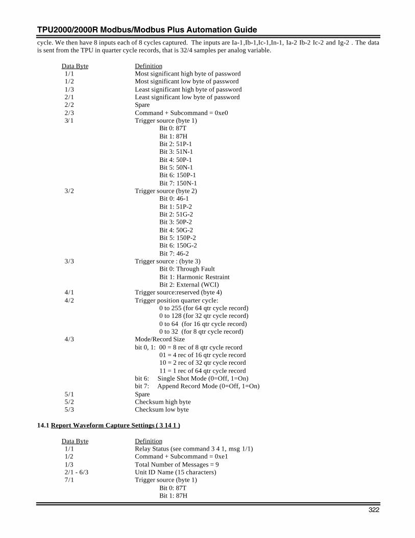
TPU2000/2000R Modbus/Modbus Plus Automation Guide
322
cycle. We then have 8 inputs each of 8 cycles captured. The inputs are Ia-1,Ib-1,Ic-1,In-1, Ia-2 Ib-2 Ic-2 and Ig-2 . The datais sent from the TPU in quarter cycle records, that is 32/4 samples per analog variable.
Data Byte Definition 1/1 Most significant high byte of password 1/2 Most significant low byte of password 1/3 Least significant high byte of password 2/1 Least significant low byte of password 2/2 Spare 2/3 Command + Subcommand = 0xe0 3/1 Trigger source (byte 1)
Bit 0: 87TBit 1: 87HBit 2: 51P-1Bit 3: 51N-1Bit 4: 50P-1Bit 5: 50N-1Bit 6: 150P-1Bit 7: 150N-1
3/2 Trigger source (byte 2)Bit 0: 46-1Bit 1: 51P-2Bit 2: 51G-2Bit 3: 50P-2Bit 4: 50G-2Bit 5: 150P-2Bit 6: 150G-2Bit 7: 46-2
3/3 Trigger source : (byte 3) Bit 0: Through Fault
Bit 1: Harmonic RestraintBit 2: External (WCI)
4/1 Trigger source:reserved (byte 4) 4/2 Trigger position quarter cycle:
0 to 255 (for 64 qtr cycle record)0 to 128 (for 32 qtr cycle record)0 to 64 (for 16 qtr cycle record)0 to 32 (for 8 qtr cycle record)
4/3 Mode/Record Sizebit 0, 1: 00 = 8 rec of 8 qtr cycle record
01 = 4 rec of 16 qtr cycle record10 = 2 rec of 32 qtr cycle record11 = 1 rec of 64 qtr cycle record
bit 6: Single Shot Mode (0=Off, 1=On)bit 7: Append Record Mode (0=Off, 1=On)
5/1 Spare 5/2 Checksum high byte 5/3 Checksum low byte
14.1 Report Waveform Capture Settings ( 3 14 1 )
Data Byte Definition 1/1 Relay Status (see command 3 4 1, msg 1/1) 1/2 Command + Subcommand = 0xe1 1/3 Total Number of Messages = 9 2/1 - 6/3 Unit ID Name (15 characters) 7/1 Trigger source (byte 1)
Bit 0: 87TBit 1: 87H
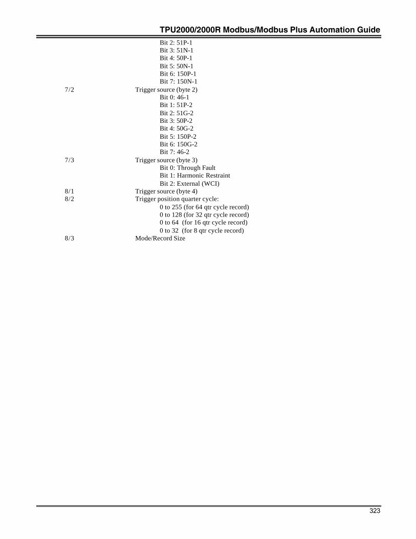
TPU2000/2000R Modbus/Modbus Plus Automation Guide
323
Bit 2: 51P-1Bit 3: 51N-1Bit 4: 50P-1Bit 5: 50N-1Bit 6: 150P-1Bit 7: 150N-1
7/2 Trigger source (byte 2)Bit 0: 46-1Bit 1: 51P-2Bit 2: 51G-2Bit 3: 50P-2Bit 4: 50G-2Bit 5: 150P-2Bit 6: 150G-2Bit 7: 46-2
7/3 Trigger source (byte 3) Bit 0: Through Fault
Bit 1: Harmonic RestraintBit 2: External (WCI)
8/1 Trigger source (byte 4) 8/2 Trigger position quarter cycle:
0 to 255 (for 64 qtr cycle record)0 to 128 (for 32 qtr cycle record)0 to 64 (for 16 qtr cycle record)0 to 32 (for 8 qtr cycle record)
8/3 Mode/Record Size
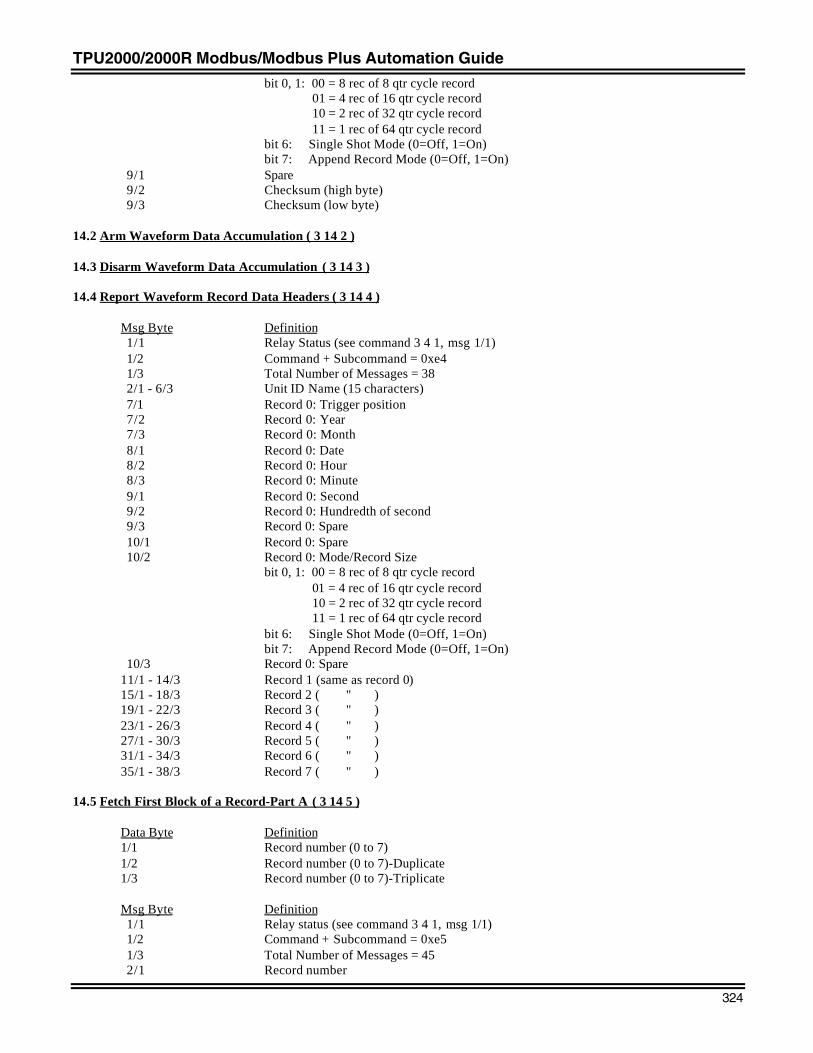
TPU2000/2000R Modbus/Modbus Plus Automation Guide
324
bit 0, 1: 00 = 8 rec of 8 qtr cycle record01 = 4 rec of 16 qtr cycle record10 = 2 rec of 32 qtr cycle record11 = 1 rec of 64 qtr cycle record
bit 6: Single Shot Mode (0=Off, 1=On)bit 7: Append Record Mode (0=Off, 1=On)
9/1 Spare 9/2 Checksum (high byte) 9/3 Checksum (low byte)
14.2 Arm Waveform Data Accumulation ( 3 14 2 )
14.3 Disarm Waveform Data Accumulation ( 3 14 3 )
14.4 Report Waveform Record Data Headers ( 3 14 4 )
Msg Byte Definition 1/1 Relay Status (see command 3 4 1, msg 1/1) 1/2 Command + Subcommand = 0xe4
1/3 Total Number of Messages = 38 2/1 - 6/3 Unit ID Name (15 characters) 7/1 Record 0: Trigger position 7/2 Record 0: Year 7/3 Record 0: Month 8/1 Record 0: Date 8/2 Record 0: Hour 8/3 Record 0: Minute 9/1 Record 0: Second 9/2 Record 0: Hundredth of second 9/3 Record 0: Spare 10/1 Record 0: Spare 10/2 Record 0: Mode/Record Size
bit 0, 1: 00 = 8 rec of 8 qtr cycle record01 = 4 rec of 16 qtr cycle record10 = 2 rec of 32 qtr cycle record11 = 1 rec of 64 qtr cycle record
bit 6: Single Shot Mode (0=Off, 1=On)bit 7: Append Record Mode (0=Off, 1=On)
10/3 Record 0: Spare11/1 - 14/3 Record 1 (same as record 0)15/1 - 18/3 Record 2 ( " )19/1 - 22/3 Record 3 ( " )23/1 - 26/3 Record 4 ( " )27/1 - 30/3 Record 5 ( " )31/1 - 34/3 Record 6 ( " )35/1 - 38/3 Record 7 ( " )
14.5 Fetch First Block of a Record-Part A ( 3 14 5 )
Data Byte Definition1/1 Record number (0 to 7)1/2 Record number (0 to 7)-Duplicate1/3 Record number (0 to 7)-Triplicate
Msg Byte Definition 1/1 Relay status (see command 3 4 1, msg 1/1) 1/2 Command + Subcommand = 0xe5
1/3 Total Number of Messages = 45 2/1 Record number
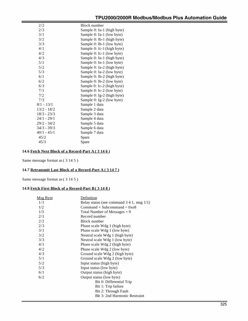
TPU2000/2000R Modbus/Modbus Plus Automation Guide
325
2/2 Block number 2/3 Sample 0: Ia-1 (high byte) 3/1 Sample 0: Ia-1 (low byte) 3/2 Sample 0: Ib-1 (high byte) 3/3 Sample 0: Ib-1 (low byte) 4/1 Sample 0: Ic-1 (high byte) 4/2 Sample 0: Ic-1 (low byte) 4/3 Sample 0: In-1 (high byte) 5/1 Sample 0: In-1 (low byte) 5/2 Sample 0: Ia-2 (high byte) 5/3 Sample 0: Ia-2 (low byte) 6/1 Sample 0: Ib-2 (high byte) 6/2 Sample 0: Ib-2 (low byte) 6/3 Sample 0: Ic-2 (high byte) 7/1 Sample 0: Ic-2 (low byte) 7/2 Sample 0: Ig-2 (high byte) 7/3 Sample 0: Ig-2 (low byte)8/1 - 13/1 Sample 1 data13/2 - 18/2 Sample 2 data18/3 - 23/3 Sample 3 data24/1 - 29/1 Sample 4 data29/2 - 34/2 Sample 5 data34/3 - 39/3 Sample 6 data40/1 - 45/1 Sample 7 data 45/2 Spare 45/3 Spare
14.6 Fetch Next Block of a Record-Part A ( 3 14 6 )
Same message format as ( 3 14 5 )
14.7 Retransmit Last Block of a Record-Part A ( 3 14 7 )
Same message format as ( 3 14 5 )
14.8 Fetch First Block of a Record-Part B ( 3 14 8 )
Msg Byte Definition 1/1 Relay status (see command 3 4 1, msg 1/1) 1/2 Command + Subcommand = 0xe8
1/3 Total Number of Messages = 9 2/1 Record number 2/2 Block number 2/3 Phase scale Wdg 1 (high byte) 3/1 Phase scale Wdg 1 (low byte) 3/2 Neutral scale Wdg 1 (high byte) 3/3 Neutral scale Wdg 1 (low byte) 4/1 Phase scale Wdg 2 (high byte) 4/2 Phase scale Wdg 2 (low byte) 4/3 Ground scale Wdg 2 (high byte) 5/1 Ground scale Wdg 2 (low byte) 5/2 Input status (high byte) 5/3 Input status (low byte) 6/1 Output status (high byte) 6/2 Output status (low byte)
Bit 0: Differential Trip Bit 1: Trip failure Bit 2: Through Fault
Bit 3: 2nd Harmonic Restraint
TPU2000/2000R Modbus/Modbus Plus Automation Guide
326
Bit 4: 5th Harmonic Restraint Bit 5: All Harmonic Restraint
6/3 Pickup status (High high byte) 7/1 Pickup status (High low byte) 7/2 Pickup status (Low high byte)
Bit 0: 46-1Bit 1: 51P-2Bit 2: 51G-2Bit 3: 50P-2Bit 4: 50G-2Bit 5: 150P-2Bit 6: 150G-2Bit 7: 46-2
7/3 Pickup status (Low low byte) Bit 0: 87T
Bit 1: 87HBit 2: 51P-1Bit 3: 51N-1Bit 4: 50P-1Bit 5: 50N-1Bit 6: 150P-1Bit 7: 150N-1
8/1 Fault status (High high byte) 8/2 Fault status (High low byte) 8/3 Fault status (Low high byte)
Bit 0: 46-1Bit 1: 51P-2Bit 2: 51G-2Bit 3: 50P-2Bit 4: 50G-2Bit 5: 150P-2Bit 6: 150G-2Bit 7: 46-2
9/1 Fault status (Low low byte)Bit 0: 87TBit 1: 87HBit 2: 51P-1Bit 3: 51N-1Bit 4: 50P-1Bit 5: 50N-1Bit 6: 150P-1Bit 7: 150N-1
9/2 Spare 9/3 Spare
14.9 Fetch Next Block of a Record-Part B ( 3 14 9 )
Same message format as ( 3 14 8 )
14.10 Retransmit Last Block of a Record-Part B ( 3 14 10 )
Same message format as ( 3 14 8 )
14.11 Fetch Acquisition Status ( 3 14 11 )
Msg Byte Definition 1/1 Relay status (see command 3 4 1, msg 1/1) 1/2 Command + Subcommand = 0xeb
1/3 Total Number of Messages = 2

TPU2000/2000R Modbus/Modbus Plus Automation Guide
327
2/1 Mode/Record Sizebit 0, 1: 00 = 8 rec of 8 qtr cycle record
01 = 4 rec of 16 qtr cycle record10 = 2 rec of 32 qtr cycle record11 = 1 rec of 64 qtr cycle record
bit 6: Single Shot Mode (0=Off, 1=On)bit 7: Append Record Mode (0=Off, 1=On)
2/2 Records Remaining (Single Shot Mode Only) 2/3 State of Accumulation (0=Running, 1=Stopped)
TPU2000/2000R Modbus/Modbus Plus Automation Guide
328
Appendix B - ASCII CODEDecimal Hexadecimal ControlValue Value Character Character
0 00 NUL (CTRL @) Null1 01 SOH (CTRL A)2 02 STX ( CTRL B)3 03 ETX (CTRL C)4 04 EOT (CTRL D)5 05 ENQ (CTRL E)6 06 ACK(CTRL F)7 07 BEL (CTRL G) Beep8 08 BS (CTRL H) Backspace9 09 HT (CTRL I) Tab10 0A LF (CTRL J) Line-feed11 0B VT (CTRL K) Cursor home12 0C FF (CTRL M) Form-feed13 0D CR (CTRL N) Carriage Return (Enter)14 0E SO (CTRL O) Shift Out15 0F SI (CTRL P) Shift In16 10 DLE Data Link Escape17 11 DCI18 12 DC219 13 DC320 14 DC421 15 NAK22 16 SYN23 17 ETB24 18 CAN25 19 EM26 1A SUB27 1B ESC28 1C Cursor right29 1D Cursor left30 1E Cursor up31 1F Cursor down32 20 Space33 21 !34 22 “35 23 #36 24 $37 25 %38 26 &39 27 ‘40 28 (41 29 (42 2A *43 2B +44 2C ,45 2D -46 2E .47 2F /48 30 049 31 150 32 251 33 3
TPU2000/2000R Modbus/Modbus Plus Automation Guide
329
52 34 453 35 554 36 655 37 756 38 857 39 958 3A59 3B60 3C <61 3D62 3E >63 3F ?64 40 @65 41 A66 42 B67 43 C68 44 D69 45 E70 46 F71 47 G72 48 H73 49 I74 4A J75 4B K76 4C L77 4D M78 4E N79 4F O80 50 P81 51 Q82 52 R83 53 S84 54 T85 55 U86 56 V87 57 W88 58 X89 59 Y90 5A Z91 5B [92 5C \93 5D ]94 5E ^95 5F _96 60 `97 61 a98 62 b99 63 c100 64 d101 65 e102 66 f103 67 g104 68 h105 69 i106 6A j107 6B k108 6C l109 6D m110 6E n
TPU2000/2000R Modbus/Modbus Plus Automation Guide
330
111 6F o112 70 p113 71 q114 72 r115 73 s116 74 t117 75 u118 76 v119 77 w120 78 x121 79 y122 7A z123 7B 124 7C |125 7D 126 7E ~127 7 F DEL
TPU2000/2000R Modbus/Modbus Plus Automation Guide
331
Appendix C - Modbus Plus Communication Between an ABB ProtectiveRelay and a Modicon PLC
ABSTRACT: Modbus Plus Capable devices are continuously being introduced into the utility environment. ThisApplication Note is intended to educate the user with the method to use the protective relay and PLC’s ModbusPlus capabilities to allow for data access and control capabilities. A simple communication example is intended togive the reader a simple method to establish communication between devices using PLC Ladder Logic. ThisApplication Note relies upon the reader’s understanding of Ladder Logic programming of a Modicon PLC andModbus Plus application.
Modbus Plus General Information
Modbus Plus is a communication protocol, which encompasses the physical layer, data link, transport andapplication link layer definition within the ISO model representation. The physical layer is a hybrid-definedinterface, which allows up to 64 devices to be multi-dropped along a serial interconnection. The interface alsoallows devices to communicate to each other with a data rate (baud rate) of 1 megabaud. The combination ofprotocol implementation and baud rate selection make Modbus Plus an excellent high performance protocoldesirable for the substation environment.
However, Modbus Plus has been given additional capabilities, which exceed the benefits of a fast baud rate.Modbus Plus is based upon a hybrid implementation of HDLC (High-level Data Link Control) protocol. Thisimplementation allows multiple devices to communicate along a single cable interface. Modbus Plus allows up to32 (or 64 with the addition of repeaters) devices to communicate along a network connection. Additionally, eachdevice can be capable of transmitting/receiving data of a length of 32 data words, which can be seen by all nodes,attached to the network. Modbus Plus has the Modbus Protocol imbedded within its data transport structure.
Modbus Plus is a deterministic network in that the response time to a command can be reasonably calculated.The method of determinism employed is referred to as “Token Passing”. Please refer to both ABB and SchneiderElectric documentation referencing network throughput calculation. Each node attached to the network canread/write information in a calculated amount of time which is determined by data transferred along the networkand the amount of nodes along the network receiving the token. The amount of time in which to transfer thetoken to each network is referred to as “Token Rotation Time”.
Modbus Plus Communication Between Devices
Modicon Programmable Logic Controllers (PLC’s) can communicate with Modbus Plus Capable devices usingtwo methods: Method 1 is using Peer Cop,. Method 2 is using a Master Block.
Peer Cop is a capability used only to allow devices by Schneider Electric to communicate with each other. Itenables one device to be configured to read or write from/to each other along a Modbus Plus connection path.It’s throughput is dependent upon the Modbus Plus token rotation time.
A Master Block is the PLC’s method of using an instruction, which is inserted within the PLC’s Ladder Logic scanto access data from another Modbus Plus capable device. A Master Block performs the following data accesstasks:
• Write 4X Data to other devices• Read 4X Data from other devices• Get Local Modbus Plus Network Statistics• Clear Local Modbus Plus Network Statistics• Write Global Database• Read Global Database• Get Remote Modbus Plus Network Statistics• Clear Remote Modbus Plus Network Statistics• Obtain Node Peer Cop Health Statistics

TPU2000/2000R Modbus/Modbus Plus Automation Guide
332
Data transfer (read or write) is explained later in this document. Network Statistics is a count of each of thenode’s good / bad transmission counts. If a bad transmission occurs, the nature of the failure is tallied on a table.Local statistics are those from nodes on the same Modbus Plus network, Remote Statistics are those gatheredfrom nodes on other interconnected Modbus Plus networks.
An ABB protective relay has Modbus Plus “HOST” addressing implementation. An additional path entry isrequired for address assignment for devices which are designed with Modbus Plus “HOST” implementation. AnABB protective relay has the following Modbus Plus features available:
• Place 32 Registers of Data in the Global Database for access by other devices.• Reply to 4X Read Data Requests from a Host or PLC Device.• Perform Operations when 4X Write Data Requests are sent by a Host Device.• Respond to Local and Remote Network Statistics Requests.• Respond to Clear Local and Remote Local Statistics Requests.
In summary, the ABB protective relay responds to commands from a Modicon PLC as well as place data into theGlobal Register buffer for retrieval from a host device.
Modbus Plus Node Addressing and Path Designation
Modbus Plus Node addressing for a Modicon PLC is determined by a thumbwheel switch or dipswitchconfiguration on the appropriate PLC. Please reference the appropriate Schneider Electric Product Manual forfurther information.
Figure 1 illustrates the Modicon PLC’s resident data paths. The PLC has four data slave paths resident in itsdevice. An Additional Global Data Read Data Slave Path is available. It is through these paths that the PLC shallobtain the relay information.
Modicon PLC
Global Read Path Global Write Path
(4) Data Master Paths(4) Data Slave Paths
Program Master Path Program Slave Path
Figure 10. Typical Modicon PLC Modbus Plus Path Definition
The ABB Relay implementation host paths are shown in Figure 2. A comparison of the data paths shows thesimilarities and differences between the PLC and ABB Relay implementation.
The ABB Relay however, requires an additional path added to its base address to complete the full Modbus Plusaddress. As per the Figure 2 implementation, 8 data slave paths are incorporated within the relay. For a PLC toaccess the data within the relay, a base address of the node and one of the eight path addresses must be givenfor the address.
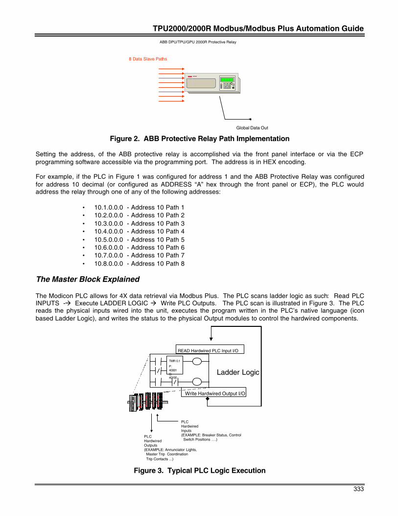
TPU2000/2000R Modbus/Modbus Plus Automation Guide
333
E
C
8 Data Slave Paths
Global Data Out
ABB DPU/TPU/GPU 2000R Protective Relay
Figure 2. ABB Protective Relay Path Implementation
Setting the address, of the ABB protective relay is accomplished via the front panel interface or via the ECPprogramming software accessible via the programming port. The address is in HEX encoding.
For example, if the PLC in Figure 1 was configured for address 1 and the ABB Protective Relay was configuredfor address 10 decimal (or configured as ADDRESS “A” hex through the front panel or ECP), the PLC wouldaddress the relay through one of any of the following addresses:
• 10.1.0.0.0 - Address 10 Path 1• 10.2.0.0.0 - Address 10 Path 2• 10.3.0.0.0 - Address 10 Path 3• 10.4.0.0.0 - Address 10 Path 4• 10.5.0.0.0 - Address 10 Path 5• 10.6.0.0.0 - Address 10 Path 6• 10.7.0.0.0 - Address 10 Path 7• 10.8.0.0.0 - Address 10 Path 8
The Master Block Explained
The Modicon PLC allows for 4X data retrieval via Modbus Plus. The PLC scans ladder logic as such: Read PLCINPUTS -à Execute LADDER LOGIC à Write PLC Outputs. The PLC scan is illustrated in Figure 3. The PLCreads the physical inputs wired into the unit, executes the program written in the PLC’s native language (iconbased Ladder Logic), and writes the status to the physical Output modules to control the hardwired components.
TMR 0.1
P:40001C;40100
Ladder Logic
PLCHardwiredOutputs(EXAMPLE: Annunciator Lights, Master Trip Coordination Trip Contacts ...)
READ Hardwired PLC Input I/O
Write Hardwired Output I/O
PLCHardwiredInputs(EXAMPLE: Breaker Status, Control Switch Positions ….)
Figure 3. Typical PLC Logic Execution
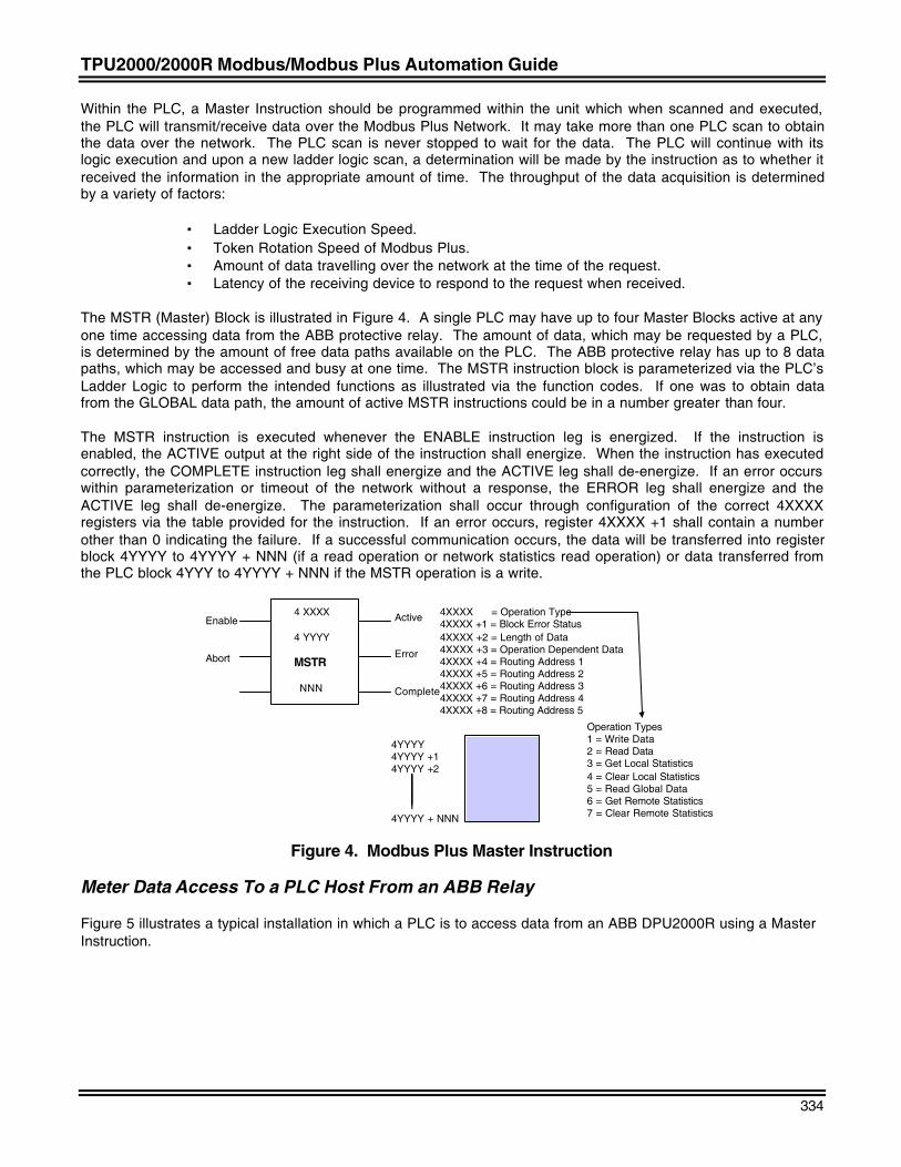
TPU2000/2000R Modbus/Modbus Plus Automation Guide
334
Within the PLC, a Master Instruction should be programmed within the unit which when scanned and executed,the PLC will transmit/receive data over the Modbus Plus Network. It may take more than one PLC scan to obtainthe data over the network. The PLC scan is never stopped to wait for the data. The PLC will continue with itslogic execution and upon a new ladder logic scan, a determination will be made by the instruction as to whether itreceived the information in the appropriate amount of time. The throughput of the data acquisition is determinedby a variety of factors:
• Ladder Logic Execution Speed.• Token Rotation Speed of Modbus Plus.• Amount of data travelling over the network at the time of the request.• Latency of the receiving device to respond to the request when received.
The MSTR (Master) Block is illustrated in Figure 4. A single PLC may have up to four Master Blocks active at anyone time accessing data from the ABB protective relay. The amount of data, which may be requested by a PLC,is determined by the amount of free data paths available on the PLC. The ABB protective relay has up to 8 datapaths, which may be accessed and busy at one time. The MSTR instruction block is parameterized via the PLC’sLadder Logic to perform the intended functions as illustrated via the function codes. If one was to obtain datafrom the GLOBAL data path, the amount of active MSTR instructions could be in a number greater than four.
The MSTR instruction is executed whenever the ENABLE instruction leg is energized. If the instruction isenabled, the ACTIVE output at the right side of the instruction shall energize. When the instruction has executedcorrectly, the COMPLETE instruction leg shall energize and the ACTIVE leg shall de-energize. If an error occurswithin parameterization or timeout of the network without a response, the ERROR leg shall energize and theACTIVE leg shall de-energize. The parameterization shall occur through configuration of the correct 4XXXXregisters via the table provided for the instruction. If an error occurs, register 4XXXX +1 shall contain a numberother than 0 indicating the failure. If a successful communication occurs, the data will be transferred into registerblock 4YYYY to 4YYYY + NNN (if a read operation or network statistics read operation) or data transferred fromthe PLC block 4YYY to 4YYYY + NNN if the MSTR operation is a write.
Enable
Abort
Active
Error
Complete
4 XXXX
4 YYYY
MSTR
NNN
4XXXX = Operation Type4XXXX +1 = Block Error Status4XXXX +2 = Length of Data4XXXX +3 = Operation Dependent Data4XXXX +4 = Routing Address 14XXXX +5 = Routing Address 24XXXX +6 = Routing Address 34XXXX +7 = Routing Address 44XXXX +8 = Routing Address 5
Operation Types1 = Write Data2 = Read Data3 = Get Local Statistics4 = Clear Local Statistics5 = Read Global Data6 = Get Remote Statistics7 = Clear Remote Statistics
4YYYY4YYYY +14YYYY +2
4YYYY + NNN
Figure 4. Modbus Plus Master Instruction
Meter Data Access To a PLC Host From an ABB Relay
Figure 5 illustrates a typical installation in which a PLC is to access data from an ABB DPU2000R using a MasterInstruction.
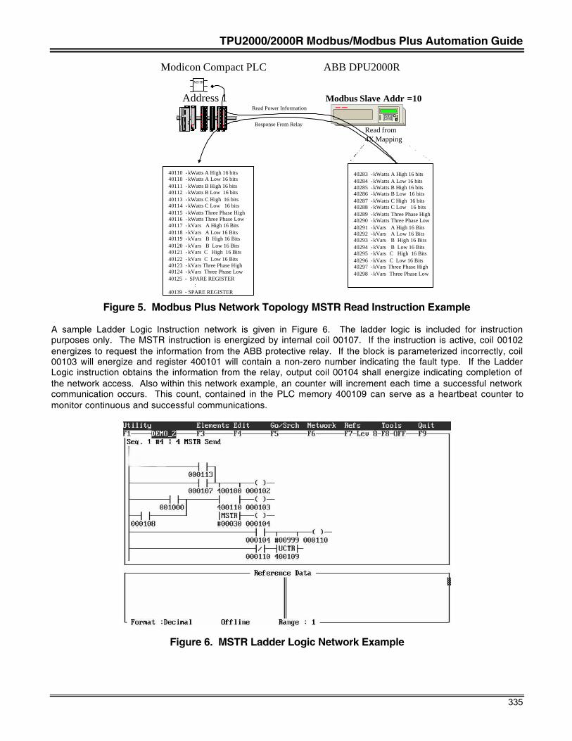
TPU2000/2000R Modbus/Modbus Plus Automation Guide
335
Address 1
EC
Modbus Slave Addr =10
Read from 4X Mapping
40283 - kWatts A High 16 bits40284 - kWatts A Low 16 bits40285 - kWatts B High 16 bits40286 - kWatts B Low 16 bits40287 - kWatts C High 16 bits40288 - kWatts C Low 16 bits40289 - kWatts Three Phase High40290 - kWatts Three Phase Low40291 - kVars A High 16 Bits40292 - kVars A Low 16 Bits40293 - kVars B High 16 Bits40294 - kVars B Low 16 Bits40295 - kVars C High 16 Bits40296 - kVars C Low 16 Bits40297 - kVars Three Phase High40298 - kVars Three Phase Low
Read Power Information
Response From Relay
40110 - kWatts A High 16 bits40110 - kWatts A Low 16 bits40111 - kWatts B High 16 bits40112 - kWatts B Low 16 bits40113 - kWatts C High 16 bits40114 - kWatts C Low 16 bits40115 - kWatts Three Phase High40116 - kWatts Three Phase Low40117 - kVars A High 16 Bits40118 - kVars A Low 16 Bits40119 - kVars B High 16 Bits40120 - kVars B Low 16 Bits40121 - kVars C High 16 Bits40122 - kVars C Low 16 Bits40123 - kVars Three Phase High40124 - kVars Three Phase Low40125 - SPARE REGISTER :40139 - SPARE REGISTER
Modicon Compact PLC ABB DPU2000RMSTR
Figure 5. Modbus Plus Network Topology MSTR Read Instruction Example
A sample Ladder Logic Instruction network is given in Figure 6. The ladder logic is included for instructionpurposes only. The MSTR instruction is energized by internal coil 00107. If the instruction is active, coil 00102energizes to request the information from the ABB protective relay. If the block is parameterized incorrectly, coil00103 will energize and register 400101 will contain a non-zero number indicating the fault type. If the LadderLogic instruction obtains the information from the relay, output coil 00104 shall energize indicating completion ofthe network access. Also within this network example, an counter will increment each time a successful networkcommunication occurs. This count, contained in the PLC memory 400109 can serve as a heartbeat counter tomonitor continuous and successful communications.
Figure 6. MSTR Ladder Logic Network Example
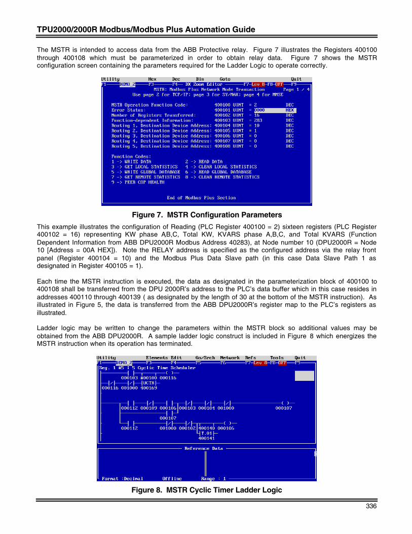
TPU2000/2000R Modbus/Modbus Plus Automation Guide
336
The MSTR is intended to access data from the ABB Protective relay. Figure 7 illustrates the Registers 400100through 400108 which must be parameterized in order to obtain relay data. Figure 7 shows the MSTRconfiguration screen containing the parameters required for the Ladder Logic to operate correctly.
Figure 7. MSTR Configuration ParametersThis example illustrates the configuration of Reading (PLC Register 400100 = 2) sixteen registers (PLC Register400102 = 16) representing KW phase A,B,C, Total KW, KVARS phase A,B,C, and Total KVARS (FunctionDependent Information from ABB DPU2000R Modbus Address 40283), at Node number 10 (DPU2000R = Node10 [Address = 00A HEX]). Note the RELAY address is specified as the configured address via the relay frontpanel (Register 400104 = 10) and the Modbus Plus Data Slave path (in this case Data Slave Path 1 asdesignated in Register 400105 = 1).
Each time the MSTR instruction is executed, the data as designated in the parameterization block of 400100 to400108 shall be transferred from the DPU 2000R’s address to the PLC’s data buffer which in this case resides inaddresses 400110 through 400139 ( as designated by the length of 30 at the bottom of the MSTR instruction). Asillustrated in Figure 5, the data is transferred from the ABB DPU2000R’s register map to the PLC’s registers asillustrated.
Ladder logic may be written to change the parameters within the MSTR block so additional values may beobtained from the ABB DPU2000R. A sample ladder logic construct is included in Figure 8 which energizes theMSTR instruction when its operation has terminated.
Figure 8. MSTR Cyclic Timer Ladder Logic
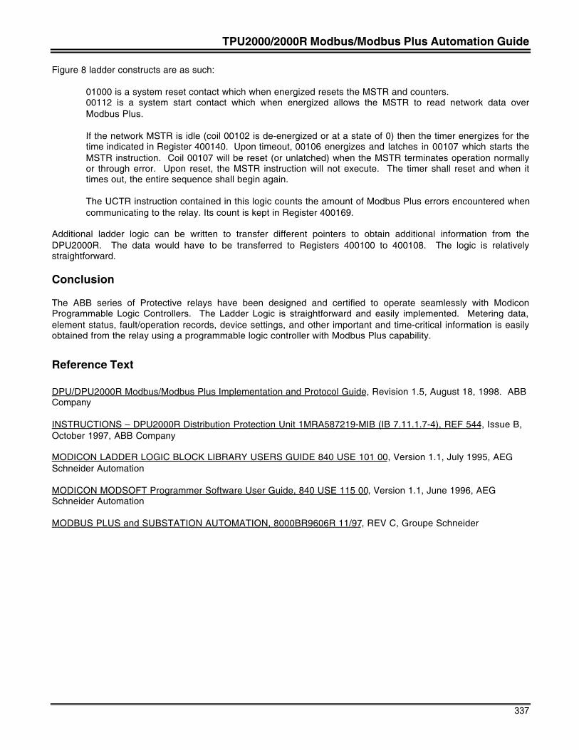
TPU2000/2000R Modbus/Modbus Plus Automation Guide
337
Figure 8 ladder constructs are as such:
01000 is a system reset contact which when energized resets the MSTR and counters.00112 is a system start contact which when energized allows the MSTR to read network data overModbus Plus.
If the network MSTR is idle (coil 00102 is de-energized or at a state of 0) then the timer energizes for thetime indicated in Register 400140. Upon timeout, 00106 energizes and latches in 00107 which starts theMSTR instruction. Coil 00107 will be reset (or unlatched) when the MSTR terminates operation normallyor through error. Upon reset, the MSTR instruction will not execute. The timer shall reset and when ittimes out, the entire sequence shall begin again.
The UCTR instruction contained in this logic counts the amount of Modbus Plus errors encountered whencommunicating to the relay. Its count is kept in Register 400169.
Additional ladder logic can be written to transfer different pointers to obtain additional information from theDPU2000R. The data would have to be transferred to Registers 400100 to 400108. The logic is relativelystraightforward.
Conclusion
The ABB series of Protective relays have been designed and certified to operate seamlessly with ModiconProgrammable Logic Controllers. The Ladder Logic is straightforward and easily implemented. Metering data,element status, fault/operation records, device settings, and other important and time-critical information is easilyobtained from the relay using a programmable logic controller with Modbus Plus capability.
Reference Text
DPU/DPU2000R Modbus/Modbus Plus Implementation and Protocol Guide, Revision 1.5, August 18, 1998. ABBCompany
INSTRUCTIONS – DPU2000R Distribution Protection Unit 1MRA587219-MIB (IB 7.11.1.7-4), REF 544, Issue B,October 1997, ABB Company
MODICON LADDER LOGIC BLOCK LIBRARY USERS GUIDE 840 USE 101 00, Version 1.1, July 1995, AEGSchneider Automation
MODICON MODSOFT Programmer Software User Guide, 840 USE 115 00, Version 1.1, June 1996, AEGSchneider Automation
MODBUS PLUS and SUBSTATION AUTOMATION, 8000BR9606R 11/97, REV C, Groupe Schneider
TPU2000/2000R Modbus/Modbus Plus Automation Guide
338
Appendix D- TELEBYTE RS 232/485 Converter Connection ToABB Protective Relays
ABSTRACT: There are many RS 232 to RS 485 converters on the market. Although ABB cannot and does notendorser a particular manufacturer of product, it does document several manufacturers’ products with their use insystems using ABB protective relays. This application note illustrates the setup and connection of the TELEBYTEModel 245 optically isolated RS 232 to RS485 (2-wire/4wire) physical interface converter.
Typical Installation
The ABB protective relay is designed with a variety of physical communication interfaces. The ABB distributionrelays such as the MSOC, GPU 2000R, TPU 2000R, DPU 2000R, DPU 2000, DPU 2000 and DPU 1500R areavailable with an RS 232, and/or RS 485 port(s).
Other devices such as the PONI M card for the REL 356 have only an RS 485 port.
Many host devices only have an RS 232 port(s). A method to connect such a device is required. Severalconverters are available to transform the physical interface on a device from RS 232 to RS 485. The advantagesof RS 485 are that many devices may be attached to a single host in a multi-drop topology. RS 485 maycommunicate with up to 32 devices with an addressable protocol. An advantage of the Telebyte 245 converter isthat, like the ABB protective relay, it is an isolated device.
General Information
Figure 1 illustrates the packaging of the Telebyte converter. The Telebyte Converter has two sets of red LED’sindicating transmission and reception of information on its ports. One set of LED’s indicatestransmission/reception of data on its RS 232 port. The second set of LED’s indicates transmission/reception ofdata on its RS 232/RS 485 port. These LED’s are invaluable in visual troubleshooting of communications.
The Telebyte converter has two sets of dB 25 connectors. One connector is a standard RS 232 interfacewhereas the other connector is the RS 485/RS 422 interface. Switches 1 and 2 configure the RS 485 interface.A DTE/DCE (Data Terminal Emulation / Data Communication Emulation) switch configures the RS 232 pinsdetermining where the data is expected (DTE = Data is Transmitted on Pin 2 and Data is Receive on Pin 3| DCE= Data is Transmitted on Pin 3 and Data is Received on Pin 2) on the RS 232 interface. Furthermore, Switch 2configures the RS 485-control mode from the RS 232 port. In two-wire emulation, data control may occur fromthe RS 232 port’s RTS (Request To Send) line or whether the data on the TD (Transmitted Data) pin is sensed. Ifthe ABB device is a MSOC, GPU 2000R, TPU 2000R, DPU 2000R, DPU 2000, DPU 2000 and DPU 1500R, nodata handshaking is permitted, thus the RS 232/485 converter must be configured for TD (Transmitted Data)mode. However, if the device attaching to the RS 232 port is a host which utilizes RTS/CTS (Request To Send/Clear To Send) handshaking, the unit must be configured using the RTS dipswitch settings as illustrated in Figure1. Additional information on the TELEBYTE 245 Optically Isolated converter is available on their website atwww.telebyteusa.com.
There are several steps required to successfully install a communication network using a physical interfaceconverter. They are:1. Knowledge of the RS 232 interfaces. (What type of handshaking is employed?, Is the port DCE or DTE
emulation?, Does the program executing on the attached device require certain signals such as CTS [ClearTo Send], RTS [Request To Send], CD [ Carrier Detect], DTR [Data Terminal Ready])? , What is the voltageof the RS 232 interface signals?)
2. Knowledge of the available power required. (If the converter requires external power, what is the voltagerequired?)
3. Knowledge of the RS 485 devices connected (2 Wire or 4 Wire?, Biasing Required?, Length of network?,Number of Devices Attached? Are the devices isolated?)
4. Proper installation of bias resistors.
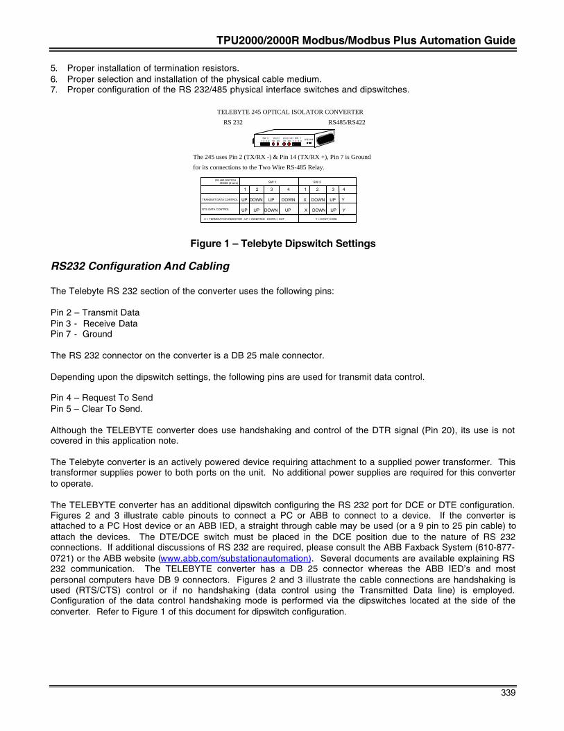
TPU2000/2000R Modbus/Modbus Plus Automation Guide
339
5. Proper installation of termination resistors.6. Proper selection and installation of the physical cable medium.7. Proper configuration of the RS 232/485 physical interface switches and dipswitches.
SW 11 2 3 4
SW 21 2 3 4
RS232TD RD
RS422/485TD RD
TELEBYTE 245 OPTICAL ISOLATOR CONVERTER
The 245 uses Pin 2 (TX/RX -) & Pin 14 (TX/RX +), Pin 7 is Ground
for its connections to the Two Wire RS-485 Relay.
RS 232 RS485/RS422
SW 1 SW 2
1 2 3 4 1 2 3 4 UP DOWN UP DOWN X DOWN UP Y
UP UP DOWN UP X DOWN UP Y
RS 485 SWITCH MODE (2 wire)
TRANSMIT DATA CONTROL
RTS DATA CONTROL
X = TERMINATION RESISTOR , UP = INSERTED : DOWN = OUT Y = DON’T CARE
DTE DCE
Figure 1 – Telebyte Dipswitch Settings
RS232 Configuration And Cabling
The Telebyte RS 232 section of the converter uses the following pins:
Pin 2 – Transmit DataPin 3 - Receive DataPin 7 - Ground
The RS 232 connector on the converter is a DB 25 male connector.
Depending upon the dipswitch settings, the following pins are used for transmit data control.
Pin 4 – Request To SendPin 5 – Clear To Send.
Although the TELEBYTE converter does use handshaking and control of the DTR signal (Pin 20), its use is notcovered in this application note.
The Telebyte converter is an actively powered device requiring attachment to a supplied power transformer. Thistransformer supplies power to both ports on the unit. No additional power supplies are required for this converterto operate.
The TELEBYTE converter has an additional dipswitch configuring the RS 232 port for DCE or DTE configuration.Figures 2 and 3 illustrate cable pinouts to connect a PC or ABB to connect to a device. If the converter isattached to a PC Host device or an ABB IED, a straight through cable may be used (or a 9 pin to 25 pin cable) toattach the devices. The DTE/DCE switch must be placed in the DCE position due to the nature of RS 232connections. If additional discussions of RS 232 are required, please consult the ABB Faxback System (610-877-0721) or the ABB website (www.abb.com/substationautomation). Several documents are available explaining RS232 communication. The TELEBYTE converter has a DB 25 connector whereas the ABB IED’s and mostpersonal computers have DB 9 connectors. Figures 2 and 3 illustrate the cable connections are handshaking isused (RTS/CTS) control or if no handshaking (data control using the Transmitted Data line) is employed.Configuration of the data control handshaking mode is performed via the dipswitches located at the side of theconverter. Refer to Figure 1 of this document for dipswitch configuration.
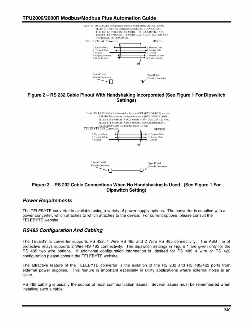
TPU2000/2000R Modbus/Modbus Plus Automation Guide
340
TELEBYTE 245 Converter DEVICE
3 Receive Data 2 Transmit Data2 Transmit Data 3 Receive Data7 Ground 5 Ground4 Request To Send 7 Request To Send5 Clear To Send 8 Clear To Send
25 pin D shellFemale Connector
9 pin D shellFemale Connector
Cable “A”- RS 232 Cable for Connection from a NODE (DTE OR DCE) and the TELEBYTE converter configured correctly (DTE DEVICE AND TELEBYTE SWITCH IN DCE MODE --OR-- DCE DEVICE AND TELEBYTE SWITCH IN DTE MODE). DATA CONTROL RTS/CTS HANDSHAKING EMPLOYED.
Figure 2 – RS 232 Cable Pinout With Handshaking Incorporated (See Figure 1 For DipswitchSettings)
TELEBYTE 245 Converter DEVICE3 Receive Data 2 Transmit Data2 Transmit Data 3 Receive Data7 Ground 5 Ground
25 pin D shellFemale Connector
9 pin D shellFemale Connector
Cable “A”- RS 232 Cable for Connection from a NODE (DTE OR DCE) and the TELEBYTE converter configured correctly (DTE DEVICE AND TELEBYTE SWITCH IN DCE MODE --OR-- DCE DEVICE AND TELEBYTE SWITCH IN DTE MODE). NO HANDSHAKING Data Control via the Transmitted Data (TD) line.
Figure 3 – RS 232 Cable Connections When No Handshaking Is Used. (See Figure 1 ForDipswitch Setting)
Power Requirements
The TELEBYTE converter is available using a variety of power supply options. The converter is supplied with apower converter, which attaches to which attaches to the device. For current options, please consult theTELEBYTE website.
RS485 Configuration And Cabling
The TELEBYTE converter supports RS 422, 4 Wire RS 485 and 2 Wire RS 485 connectivity. The ABB line ofprotective relays supports 2 Wire RS 485 connectivity. The dipswitch settings in Figure 1 are given only for theRS 485 two wire options. If additional configuration information is desired for RS 485 4 wire or RS 422configuration please consult the TELEBYTE website.
The attractive feature of the TELEBYTE converter is the isolation of the RS 232 and RS 485/422 ports fromexternal power supplies. This feature is important especially in utility applications where external noise is anissue.
RS 485 cabling is usually the source of most communication issues. Several issues must be remembered wheninstalling such a cable:
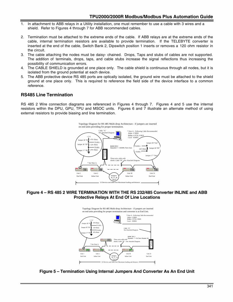
TPU2000/2000R Modbus/Modbus Plus Automation Guide
341
1. In attachment to ABB relays in a Utility installation, one must remember to use a cable with 3 wires and ashield. Refer to Figures 4 through 7 for ABB recommended cables.
2. Termination must be attached to the extreme ends of the cable. If ABB relays are at the extreme ends of thecable, internal termination resistors are available to provide termination. If the TELEBYTE converter isinserted at the end of the cable, Switch Bank 2, Dipswitch position 1 inserts or removes a 120 ohm resistor inthe circuit.
3. The cable attaching the nodes must be daisy- chained. Drops, Taps and stubs of cables are not supported.The addition of terminals, drops, taps, and cable stubs increase the signal reflections thus increasing thepossibility of communication errors.
4. The CABLE SHIELD is grounded at one place only. The cable shield is continuous through all nodes, but it isisolated from the ground potential at each device.
5. The ABB protective device RS 485 ports are optically isolated, the ground wire must be attached to the shieldground at one place only. This is required to reference the field side of the device interface to a commonreference.
RS485 Line Termination
RS 485 2 Wire connection diagrams are referenced in Figures 4 through 7. Figures 4 and 5 use the internalresistors within the DPU, GPU, TPU and MSOC units. Figures 6 and 7 illustrate an alternate method of usingexternal resistors to provide biasing and line termination.
Cable “A”See Attached Diagram
ECEC EC
32 Devices and 3000 Feet Maximum loading and distance.
EC
Unit 1 Unit 2 Unit 30 Unit 31
Three-wire cable withshield. Cable “B” - See Attached Diagram.
End Unit Inline Unit Inline Unit End UnitJumpersJ6, J7, J8 “OUT”
+ 5 V
120 Ohms
470 Ohms
470 Ohms
Jumper J8 “IN
Jumper J 7 “IN”
Jumper J6 “IN”TX/RX +
TX/RX -
Topology Diagram for RS 485 Multi-drop Architecture - if jumpers are insertedon end units providing for proper termination.
* See Note A.
* Note A - Following Cable Recommended Alpha # 58902 Belden # 9729, # 9829 Carol #58902
120 Ohms
Jumper J8 “Out”
Jumper J6 “IN”TX/RX +
TX/RX -
Jumper J 7 “Out”
TELE
BY
TE 245
RS
232/ RS
422/485
BANK SW 2Dipswitch 1 = DOWN (Term Out)
Figure 4 – RS 485 2 WIRE TERMINATION WITH THE RS 232/485 Converter INLINE and ABBProtective Relays At End Of Line Locations
Cable “A”See Attached Diagram
ECEC
EC
32 Devices and 3000 Feet Maximum loading and distance.
EC
Unit 1 Unit 2 Unit 30 Unit 31
Three-wire cable withshield. Cable “B” - See Attached Diagram.
End Unit Inline Unit Inline Unit End UnitJumpersJ6, J7, J8 “OUT”
+ 5 V
120 Ohms
470 Ohms
470 Ohms
Jumper J8 “IN
Jumper J 7 “IN”
Jumper J6 “IN”TX/RX +
TX/RX -
Topology Diagram for RS 485 Multi-drop Architecture - if jumpers are insertedon end units providing for proper termination and converter is at End Unit.
* See Note A.
* Note A - Following Cable Recommended Alpha # 58902 Belden # 9729, # 9829 Carol #58902
TELE
BY
TE 245
RS
232/ RS
422/485
BANK SW 2Dipswitch 1 = IN (Term Resistor IN)
Figure 5 – Termination Using Internal Jumpers And Converter As An End Unit
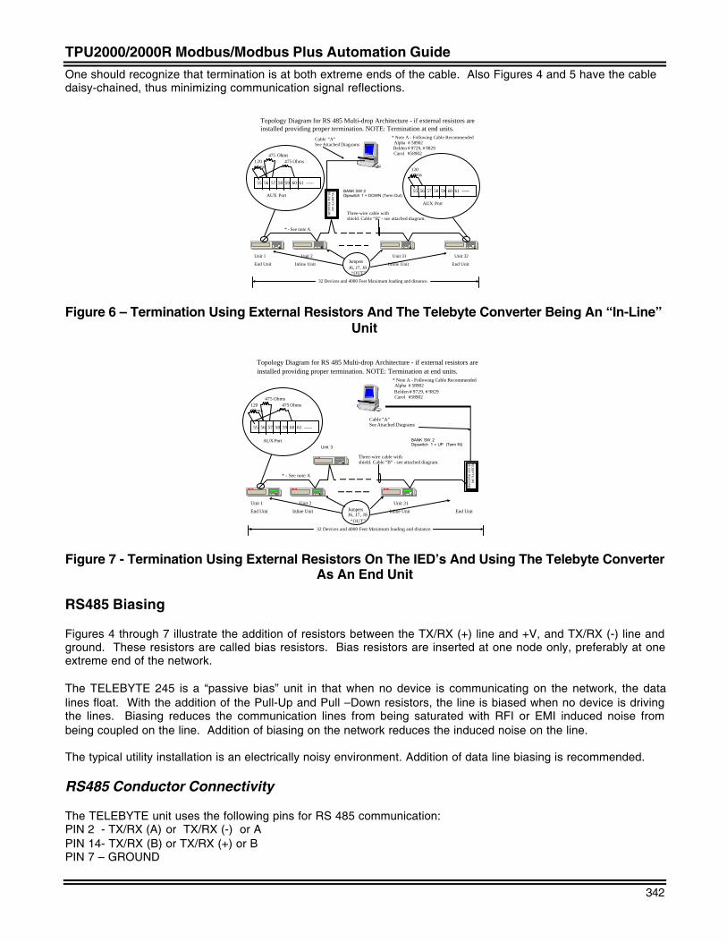
TPU2000/2000R Modbus/Modbus Plus Automation Guide
342
One should recognize that termination is at both extreme ends of the cable. Also Figures 4 and 5 have the cabledaisy-chained, thus minimizing communication signal reflections.
Cable “A”See Attached Diagrams
ECEC EC
32 Devices and 4000 Feet Maximum loading and distance.
EC
Unit 1 Unit 2 Unit 31 Unit 32
Three-wire cable withshield. Cable “B” - see attached diagram.
End Unit Inline Unit Inline Unit End UnitJumpersJ6, J7, J8 “OUT”
Topology Diagram for RS 485 Multi-drop Architecture - if external resistors areinstalled providing proper termination. NOTE: Termination at end units.
55 56 57 58 59 60 61 -----
475 Ohms475 Ohms
120Ohms
AUX Port
* - See note A
* Note A - Following Cable Recommended Alpha # 58902 Belden # 9729, # 9829 Carol #58902
55 56 57 58 59 60 61 -----
120Ohms
AUX Port
TE
LEB
YT
E 245
RS
232/ RS
422/485
BANK SW 2Dipswitch 1 = DOWN (Term Out)
Figure 6 – Termination Using External Resistors And The Telebyte Converter Being An “In-Line”Unit
Cable “A”See Attached Diagrams
ECEC
EC
32 Devices and 4000 Feet Maximum loading and distance.
EC
Unit 1 Unit 2 Unit 31
Three-wire cable withshield. Cable “B” - see attached diagram.
End Unit Inline Unit Inline Unit End UnitJumpersJ6, J7, J8 “OUT”
Topology Diagram for RS 485 Multi-drop Architecture - if external resistors areinstalled providing proper termination. NOTE: Termination at end units.
55 56 57 58 59 60 61 -----
475 Ohms475 Ohms
120Ohms
AUX Port
* - See note A
* Note A - Following Cable Recommended Alpha # 58902 Belden # 9729, # 9829 Carol #58902
TE
LEB
YT
E 245
RS
232/ RS
422/485
BANK SW 2Dipswitch 1 = UP (Term IN)
Unit 3
Figure 7 - Termination Using External Resistors On The IED’s And Using The Telebyte ConverterAs An End Unit
RS485 Biasing
Figures 4 through 7 illustrate the addition of resistors between the TX/RX (+) line and +V, and TX/RX (-) line andground. These resistors are called bias resistors. Bias resistors are inserted at one node only, preferably at oneextreme end of the network.
The TELEBYTE 245 is a “passive bias” unit in that when no device is communicating on the network, the datalines float. With the addition of the Pull-Up and Pull –Down resistors, the line is biased when no device is drivingthe lines. Biasing reduces the communication lines from being saturated with RFI or EMI induced noise frombeing coupled on the line. Addition of biasing on the network reduces the induced noise on the line.
The typical utility installation is an electrically noisy environment. Addition of data line biasing is recommended.
RS485 Conductor Connectivity
The TELEBYTE unit uses the following pins for RS 485 communication:PIN 2 - TX/RX (A) or TX/RX (-) or APIN 14- TX/RX (B) or TX/RX (+) or BPIN 7 – GROUND
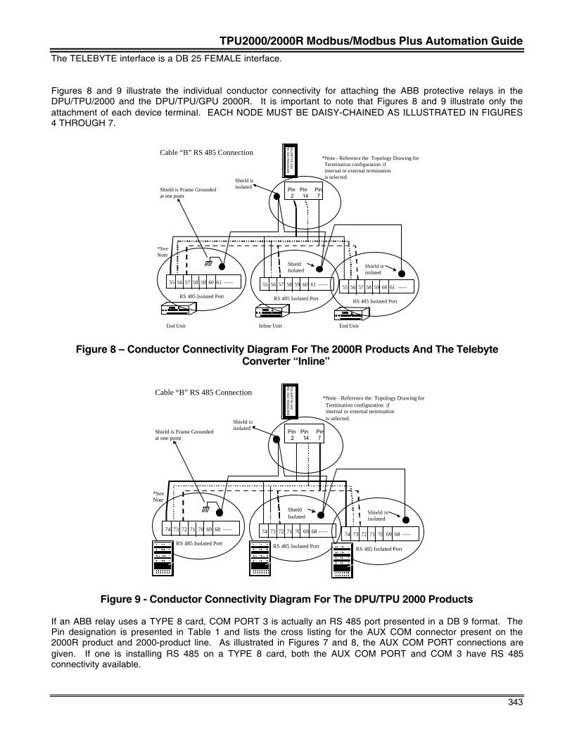
TPU2000/2000R Modbus/Modbus Plus Automation Guide
343
The TELEBYTE interface is a DB 25 FEMALE interface.
Figures 8 and 9 illustrate the individual conductor connectivity for attaching the ABB protective relays in theDPU/TPU/2000 and the DPU/TPU/GPU 2000R. It is important to note that Figures 8 and 9 illustrate only theattachment of each device terminal. EACH NODE MUST BE DAISY-CHAINED AS ILLUSTRATED IN FIGURES4 THROUGH 7.
3
55 56 57 58 59 60 61 -----
RS 485 Isolated Port
Shield is isolatedShield is Frame Grounded
at one point
3
55 56 57 58 59 60 61 -----
RS 485 Isolated Port
3
55 56 57 58 59 60 61 -----
RS 485 Isolated Port
End Unit Inline Unit End Unit
Shield Isolated
Shield isisolated
Cable “B” RS 485 Connection
*SeeNote
*Note - Reference the Topology Drawing for Termination configuration if internal or external termination is selected.
TE
LEB
YT
E 245
RS
232/ RS
422/485
Pin Pin Pin 2 14 7
Figure 8 – Conductor Connectivity Diagram For The 2000R Products And The TelebyteConverter “Inline”
74 73 72 71 70 69 68 -----
RS 485 Isolated Port
Shield is isolated
Shield is Frame Grounded at one point
74 73 72 71 70 69 68 -----
RS 485 Isolated Port
74 73 72 71 70 69 68 -----
RS 485 Isolated Port
Shield Isolated
Shield isisolated
Cable “B” RS 485 Connection
*SeeNote
*Note - Reference the Topology Drawing for Termination configuration if internal or external termination is selected.
Pin Pin Pin 2 14 7
TE
LEB
YT
E 245
RS
232/ RS
422/485
Figure 9 - Conductor Connectivity Diagram For The DPU/TPU 2000 Products
If an ABB relay uses a TYPE 8 card, COM PORT 3 is actually an RS 485 port presented in a DB 9 format. ThePin designation is presented in Table 1 and lists the cross listing for the AUX COM connector present on the2000R product and 2000-product line. As illustrated in Figures 7 and 8, the AUX COM PORT connections aregiven. If one is installing RS 485 on a TYPE 8 card, both the AUX COM PORT and COM 3 have RS 485connectivity available.
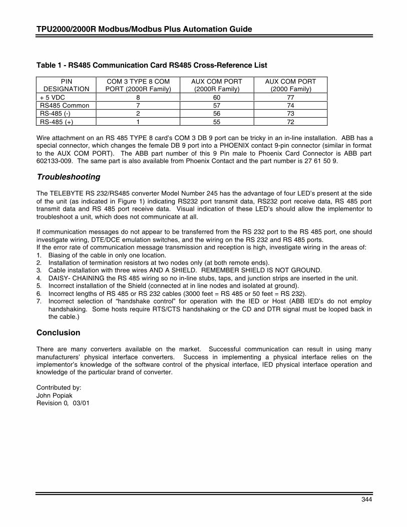
TPU2000/2000R Modbus/Modbus Plus Automation Guide
344
Table 1 - RS485 Communication Card RS485 Cross-Reference List
PINDESIGNATION
COM 3 TYPE 8 COMPORT (2000R Family)
AUX COM PORT(2000R Family)
AUX COM PORT(2000 Family)
+ 5 VDC 8 60 77RS485 Common 7 57 74RS-485 (-) 2 56 73RS-485 (+) 1 55 72
Wire attachment on an RS 485 TYPE 8 card’s COM 3 DB 9 port can be tricky in an in-line installation. ABB has aspecial connector, which changes the female DB 9 port into a PHOENIX contact 9-pin connector (similar in formatto the AUX COM PORT). The ABB part number of this 9 Pin male to Phoenix Card Connector is ABB part602133-009. The same part is also available from Phoenix Contact and the part number is 27 61 50 9.
Troubleshooting
The TELEBYTE RS 232/RS485 converter Model Number 245 has the advantage of four LED’s present at the sideof the unit (as indicated in Figure 1) indicating RS232 port transmit data, RS232 port receive data, RS 485 porttransmit data and RS 485 port receive data. Visual indication of these LED’s should allow the implementor totroubleshoot a unit, which does not communicate at all.
If communication messages do not appear to be transferred from the RS 232 port to the RS 485 port, one shouldinvestigate wiring, DTE/DCE emulation switches, and the wiring on the RS 232 and RS 485 ports.If the error rate of communication message transmission and reception is high, investigate wiring in the areas of:1. Biasing of the cable in only one location.2. Installation of termination resistors at two nodes only (at both remote ends).3. Cable installation with three wires AND A SHIELD. REMEMBER SHIELD IS NOT GROUND.4. DAISY- CHAINING the RS 485 wiring so no in-line stubs, taps, and junction strips are inserted in the unit.5. Incorrect installation of the Shield (connected at in line nodes and isolated at ground).6. Incorrect lengths of RS 485 or RS 232 cables (3000 feet = RS 485 or 50 feet = RS 232).7. Incorrect selection of “handshake control” for operation with the IED or Host (ABB IED’s do not employ
handshaking. Some hosts require RTS/CTS handshaking or the CD and DTR signal must be looped back inthe cable.)
Conclusion
There are many converters available on the market. Successful communication can result in using manymanufacturers’ physical interface converters. Success in implementing a physical interface relies on theimplementor’s knowledge of the software control of the physical interface, IED physical interface operation andknowledge of the particular brand of converter.
Contributed by:John PopiakRevision 0, 03/01

TPU2000/2000R Modbus/Modbus Plus Automation Guide
345