transcribers name: pradeep structure of materials prof...
TRANSCRIPT

Transcribers Name: Pradeep
Structure of Materials
Prof. Anandh Subramaniam
Department of Material Science and Engineering
Indian Institute of Technology, Kanpur
Lecture - 29
Defects in Crystals
After talking about surfaces in considerable detail now, we will take up the topic of
interfaces.
(Refer Slide Time: 00:41)
Interface in general can be between a solid and a liquid solid and a vapours or between a
solid. And a solid surface is nothing but a special case of an interface between a solid
and or a liquid and the vapours face or the gas face interface in general separate 2
materials. And surfaces of various kinds can be understood as special cases of an
interfaces, if you want to understand interface we can look at it. Through many points of
view like if across an interface 2 materials are the same material or a different materials.
In another word is it an homo phase interface or the hetro phase interface, we then talk
about the interface in terms the order inside the interface. And now we are talking about
the order in the interface and not in the crystals or the phase bounding the interface. So,
interfaces can be ordered or disordered from this prospective additionally.

We could also talk about the purity of an interface that is if the interface has a material
which is segregated from the bulk materials surrounding the interface. And typically it is
we noticed that if a phase or a salute atom is not soluble in any of the grains or the
phases separate around the interface then it will segregate to the interface. Then based on
the orientation of the bounding crystals, we can talk about special or low angle interfaces
or a very general kind of an interface which can be a our random mis-orientation
between the 2 interfaces. We will also consider interfaces based on the terminology
which is called coherent semi coherent or incoherent interfaces. So, this point will
become clear when we actually take up a detail study of coherent semi coherent and
incoherent interfaces. It should be noted the interfaces the once we are going to consider
in this topic are going to be solid interfaces. We will not deal with liquid vapours or
liquid liquid interfaces in this set of slides or in this set of topics and solid.
Solid interfaces play a very important role in determining the behavior of materials as
can we highlighted some examples. Obviously, this is just illustrative examples are for
example, we consider hot shortness in iron when we roll iron with some impurity of
sulphur present. Then this sulphur can segregate to the grain boundary region and form
the fes phase the iron sulphide phase of the grain boundary. And this can lead to what is
known as brittleness during lot rolling conditions, because the fes can become a liquid
phase. And the material will behave as if it is a brittle material because of the
segregation. Therefore, we want to avoid sulphur impurity segregating to the interface
and it is to be noted that this segregation is actually a very small quantities segregation. It
is not in large amount sulphur need to be present before hot shortness is observed.
Another nice striking example would be the diffusion of gallium along the grain
boundaries of the aluminum if you hold an aluminum polycrystalline material as thin
foil.
And you expose it to a gallium atmosphere by rubbing some gallium on it. Then this
gallium would tend to diffuse very fast in along the grain boundaries and if this specimen
is held in tension. Then this material would fail because gallium is liquid under room
temperature of 50 60 degree Celsius. Creep is an very important phenomenon which
leads to quite a bit of engineering failures at high temperatures. And grain boundary
sliding is one of the important mechanisms by which creep takes place. And therefore,
we can see that from these illustrative examples that interfaces play a very important role
in a diverse variety of phenomena. And it as people heard of the relationship has a very
important bearing coming from the grain boundary which we will study during this study
on interfaces.
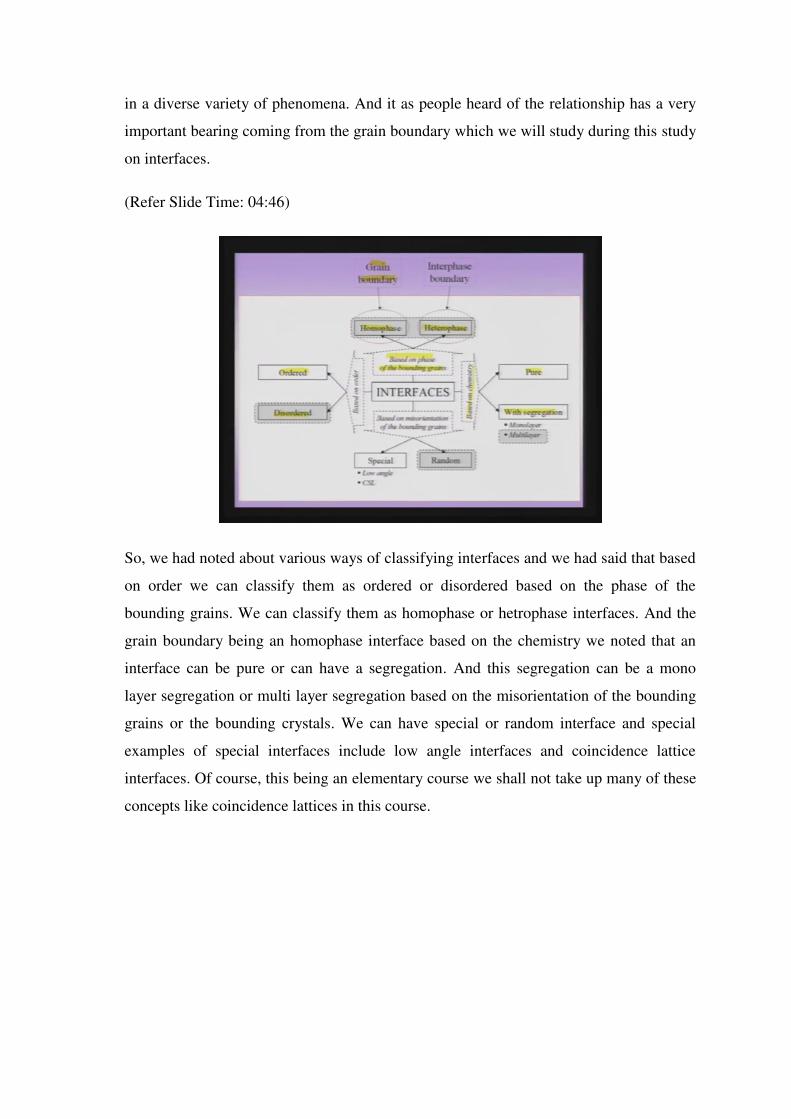
(Refer Slide Time: 04:46)
So, we had noted about various ways of classifying interfaces and we had said that based
on order we can classify them as ordered or disordered based on the phase of the
bounding grains. We can classify them as homophase or hetrophase interfaces. And the
grain boundary being an homophase interface based on the chemistry we noted that an
interface can be pure or can have a segregation. And this segregation can be a mono
layer segregation or multi layer segregation based on the misorientation of the bounding
grains or the bounding crystals. We can have special or random interface and special
examples of special interfaces include low angle interfaces and coincidence lattice
interfaces. Of course, this being an elementary course we shall not take up many of these
concepts like coincidence lattices in this course.

(Refer Slide Time: 05:42)
Let us start our discussion of interfaces with the grain boundary typically if I take a piece
of aluminum or a piece of wire of copper. It is a polycrystalline material this
polycrystalline material has single crystalline region which is bound and bounded to one
other. And the interface between this two crystallites is called grain boundary, typically a
grain boundary is considered as two dimensional plain or two dimensional surface. But,
of course, in reality the grain boundary region can extend a few atomic diameters into
either of the bounding crystals. The best way of visualizing a formation of a grain
boundary is by considering the crystallizing of a melt which we shall do now.
(Refer Slide Time: 06:32)
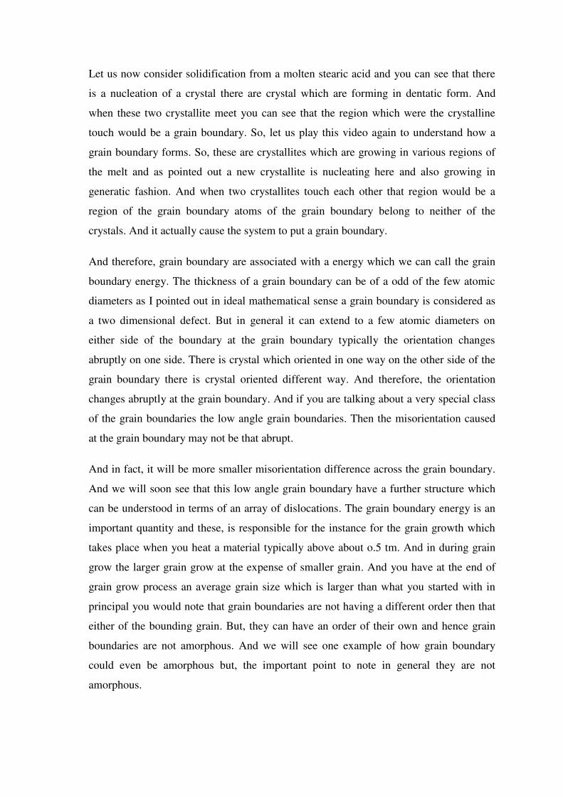
Let us now consider solidification from a molten stearic acid and you can see that there
is a nucleation of a crystal there are crystal which are forming in dentatic form. And
when these two crystallite meet you can see that the region which were the crystalline
touch would be a grain boundary. So, let us play this video again to understand how a
grain boundary forms. So, these are crystallites which are growing in various regions of
the melt and as pointed out a new crystallite is nucleating here and also growing in
generatic fashion. And when two crystallites touch each other that region would be a
region of the grain boundary atoms of the grain boundary belong to neither of the
crystals. And it actually cause the system to put a grain boundary.
And therefore, grain boundary are associated with a energy which we can call the grain
boundary energy. The thickness of a grain boundary can be of a odd of the few atomic
diameters as I pointed out in ideal mathematical sense a grain boundary is considered as
a two dimensional defect. But in general it can extend to a few atomic diameters on
either side of the boundary at the grain boundary typically the orientation changes
abruptly on one side. There is crystal which oriented in one way on the other side of the
grain boundary there is crystal oriented different way. And therefore, the orientation
changes abruptly at the grain boundary. And if you are talking about a very special class
of the grain boundaries the low angle grain boundaries. Then the misorientation caused
at the grain boundary may not be that abrupt.
And in fact, it will be more smaller misorientation difference across the grain boundary.
And we will soon see that this low angle grain boundary have a further structure which
can be understood in terms of an array of dislocations. The grain boundary energy is an
important quantity and these, is responsible for the instance for the grain growth which
takes place when you heat a material typically above about o.5 tm. And in during grain
grow the larger grain grow at the expense of smaller grain. And you have at the end of
grain grow process an average grain size which is larger than what you started with in
principal you would note that grain boundaries are not having a different order then that
either of the bounding grain. But, they can have an order of their own and hence grain
boundaries are not amorphous. And we will see one example of how grain boundary
could even be amorphous but, the important point to note in general they are not
amorphous.
(Refer Slide Time: 09:27)
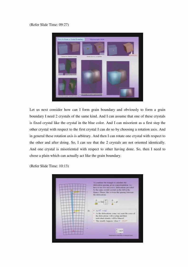
Let us next consider how can I form grain boundary and obviously to form a grain
boundary I need 2 crystals of the same kind. And I can assume that one of these crystals
is fixed crystal like the crystal in the blue color. And I can misorient as a first step the
other crystal with respect to the first crystal I can do so by choosing a rotation axis. And
in general these rotation axis is arbitrary. And then I can rotate one crystal with respect to
the other and after doing. So, I can see that the 2 crystals are not oriented identically.
And one crystal is misoriented with respect to other having done. So, then I need to
chose a plain which can actually act like the grain boundary.
(Refer Slide Time: 10:13)

Why in the grain boundaries can spontaneously form during the process known as
polyganisation which takes place during the recovery of a cold work material. Therefore,
they can have an important role in materials and as I pointed out they can spontaneously
form during recovery process. So, let us summaries how this how we understand this
dislocation along the grain boundary. So, we have a triangle here in which we have the
burgers vector which is representative of strength of the dislocation. And depending on
the burgers vector the plain the dislocation energy is returning now these dislocation
noted spacing. We have noted keeps on decreasing as we increase the misorientation
angle between two crystals. And at some point of time the individual independent
existence of these dislocations is no longer or identification is no longer possible with
increasing misorientation. And therefore, we land up with the scenario what is known as
the high angle grain boundary. And depending on the when do we actually start saying
high angle grain boundaries is determined as you can see from this equation.
(Refer Slide Time: 11:24)
Now, this is a nice example of a low angle grain boundary though not a symmetric low
angle grain boundary this material happens to be torsion tightening. And a misorientation
angle between the 2 crystallites here or a 2 grains here is about 8 degrees. And the
existence of this dislocations along the grain boundary you see in the image below which
is nothing but a Fourier filtered image in which you can see that there are distinct
dislocations which are present along the grain boundary. So, we can clearly see in high

resolution lattice using an high resolution lattice range image which is been Fourier
filtered that a low angle grain boundary consist of an array of dislocations.
Another important feature of this presence of these dislocations along a low angle grain
boundaries and as pointed out by especially why does this arrangement of dislocations
along to create low angle grain boundary take place during polygonization is that the
compressive field of one dislocation. Cancel the tensile field of the other dislocation
partially. And therefore, to such a boundary has no longer in stress field that is all the
stress field is localized to only to grain boundary region unlike an isolated dislocation.
And this is the motivation for a crystal to actually throughout such kind of low angle
grain boundaries during a polygonization process.
(Refer Slide Time: 12:41)
Now, let us consider how structural dislocation can accommodate linear midfield. So, let
us consider a nice example for this which is the growth of silicon germanium to some
composition. So, you can for example, consider silicon 50 percent germanium, 50
percent diamond cubic structure which is grown on a silicon substrate. So, this could be
the silicon substrate and this could be the G s i alloy. And if you consider silicon it is got
a four point two lattice parameter in midfield with germanium. And this alloy itself has a
lattice parameter in midfield. Therefore, with these substrate which is silicon now when
epitoxically grow such a film on the top of substrate. The film has a tetragonal distortion
and is forced to grow when especially as a thin layer on top of the silicon such that the

lattice plains are continuous here. So, you can see that in this schematic which is of
course, an exploitative schematic that lattice plains are continuous. And such a boundary
is called a coherent interface or a coherent boundary where in lattice plains are
continuous. Therefore, here is the growth of gesi on the top of Silicon. And such an alloy
grows epitoxically putting out a coherent interface.
But as a film grows thicker and thicker at some point of time or at some point of time or
some thickness of film the energy stored at the interface or stored in the film becomes
too much. And therefore, the interface breaks up into regions which are coherent or
actually taking for the whole interface as a semi coherent interface. In other words a
coherent interface becomes semi coherent by the presence of a midfield dislocation. And
this dislocation as you can see age dislocation is accommodating linear midfield between
the epitoxically film and the substrate. And again we have to note that these interfacial
dislocation are very different in characteristics as compared to a bulk dislocation. As we
have noted before in the case even in the normal material in the case of plasticity.
Therefore, you could have a coherent interface you could have a semi coherent interface
between G s and S I where in there are interfacial midfield edge dislocation present
which are partially reliving the strain between the film and the substrate. And you could
also think of an interface which is totally incoherent that means there is no matching of
plains between the two sides of the interface. And therefore, such an interface would be
an incoherent interface. So therefore, based on the continuity or coherency we can have a
coherent interface a semi coherent interface or a incoherent interface. And we can note
clearly here that this dislocation here is slightly different from the grain boundary
dislocation. Because the material above the dislocation and the material below the
dislocation slip plain is are different.
Therefore, these are hetro hepitoxial systems that is the materials above and below the
interface are different to summaries this slide. Therefore, there are structural dislocations
which can accommodate linear misfate. And such this locations are like the low angle
grain boundary dislocations localized the interface. And here they are performing the
role of partly reliving the stresses which are caused because of the lattice mismatch
between the g s i alloy and the silicon substrate. And based on coherency you can have
coherent interfaces and semi coherent interfaces which have dislocations decorating the
interface and in generally of course, an incoherent interface.
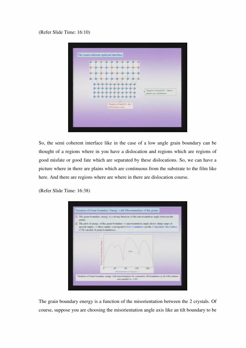
(Refer Slide Time: 16:10)
So, the semi coherent interface like in the case of a low angle grain boundary can be
thought of a regions where in you have a dislocation and regions which are regions of
good misfate or good fate which are separated by these dislocations. So, we can have a
picture where in there are plains which are continuous from the substrate to the film like
here. And there are regions where are where in there are dislocation course.
(Refer Slide Time: 16:38)
The grain boundary energy is a function of the misorientation between the 2 crystals. Of
course, suppose you are choosing the misorientation angle axis like an tilt boundary to be
a safe for an instance the 1 1 0 axis none you would if you had to plot the misorientation
angle which is theta n on the x-axis with the grain boundary energy which is the y-axis.
You typically you may end up getting a plot which looks like this the important feature
of this plot is that for low angle boundaries the energy is small. And we had noticed that
this low angle region is the region where in you can consider the grain boundary to be an
array of dislocations. Then for normal angle grain boundaries you would notice that the
energy is pretty high. But between this high energy mis-orientations there are cuts in the
grain boundary verses the mis-orientation plot that there are some special boundaries
which have a low energy. Typically such kind of boundaries or eyes when you have
some a concept known as coincidence side lattice model of grain boundaries this being a
elementary course.
We are not going in to the detail of what is a coincidence side lattice or how this
coincidence side lattice is going to give rise to low energy. But this is important to note
that the like we had noted for the case of the low angle grain boundary that the increasing
mis-orientation. The energy of the boundary is going to change so, it is true for even for
angle grain boundaries. But the variations is not a monotonic function in other words the
variation in energy of the system as a function of the grain boundary mis-orientation.
And could show a function which looks like the plot shown here which could have
curves which correspond to special boundaries. So, we could in general classified 2 kinds
of special boundaries those having which corresponds to this curves and those having
low angle. Therefore, we can have low angle grain boundaries which as special
boundaries. And those high angle grain boundaries which could also have relatively
lower energy which we can which can then corresponded to something known as
coincidence side lattice concept. But as we noted this grain boundary energy is a very
important quantity in the behavior of the material. Because now this is going to
determine how much segregation going to occur or how much of for instance grain
growth or how fast the grain growth occur during an annealing or high temperature hold
process?

(Refer Slide Time: 19:01)
As I pointed out before, suppose you had to talk to ah material scientist in the early days
that is much before some of the models of these grain boundaries worse a mental picture
which is often carried by many people is that the grain boundary is a region of disorder.
And we have as we have noted by looking at some other grain boundaries so far that
often it is not true and often there could be an order in the grain boundary. Of course, this
order could be very different from the order present in the bulk of the crystal. But there
are special cases wherein you would find actually that the grain boundary region is
actually totally amorphous or it is classy. And such an example is shown in the high
resolution lattice image which is in the micrograph as below.
So, this micrograph below shows a grain boundary in silicon nitrate between two this
grain there is a grain one of silicon nitrate above. And there is a grain two of silicon
nitrate below and there are there there fringes corresponds to lattice plain in this two
crystallites. But, the important thing to focus here is the grain boundary region. And you
would notice that the grain boundary region is glassy or amorphous so even amorphous
region at the grain boundary. But it is to be noted this it occurs in very special cases as in
this case this is silicon grain boundary in silicon nitrate. Such kind of amorphous grain
boundaries can also found in other special system like silicon carbide tension tightening
and alumina. But if you take a general grain boundary in aluminum or copper you would
not typically find these kind of amorphous grain boundary.

And to summaries this slide though most grain boundaries can have a very good order in
them. There are possibilities of having grain boundaries which have an disordered and
amorphous layer. And these examples can be found for instance in silicon nitrate or
tension tightening where in you have a thin layer. Of course, this layer is of the order of a
nano meter or 1 to 2 nano meters which is an amorphous region. And the grain boundary
region itself is totally amorphous or not does not have crystalline order as in the side of
the crystal.
(Refer Slide Time: 21:10)
The next two dimensional interface, we consider is a twin boundary. The twin boundary
is a very special kind of a boundary which is in wherein some sense very regular kind of
a boundary as compared to any other defects in the material. Or any other two
dimensional defects in a material the atomic arrangement on one side of the twin
boundary is related to other side by a symmetry operation this symmetry operation is
typically in mirror. And therefore, you have something known as mirror twin boundary
or the mirror twin. But in addition you can also have inversion twin and rotational twins
So, we will take up one example at least of a mirror twin and also of a rotational twin
during the course of these lectures. It is obvious that the symmetry operator defining the
twin itself cannot be a symmetry operator of the crystal. Because if it is a symmetry
operator of the crystal the crystal actually will continue across a interface. And therefore,
we will have no distinct boundary.

And therefore, we can have no twin that means the symmetry operator for instance some
mirror cannot be a mirror plain of the crystal that means it is not one of the existing
symmetry operators of the crystal. And it has to the mirror plain has to be different from
the symmetry operator of the crystal it is been often noted. And we will see this using a
micrograph the twin boundary typically occurs in pairs and the orientation difference
created by one twin boundary is restored by the other the region between the twin
boundaries is called the twin region or a twin. Therefore, you have a twin and the
bounding surface of the twin are called twin boundaries. We have earlier noted when
defining a crystal that a crystal can be defined with respect to a geometrical entity a
physical property or a combination of both.
Therefore when we are talking about twin which is now again a concept of invokes
symmetry therefore, like the crystal Therefore, you could have a twin boundary a mirror
twin for example, which could be reflecting physical property or which could be
reflecting atomic position. Therefore, you could have a twin boundary which is with
respect to a geometrical entity or a physical property or a very special cases. We can
even visualize a twin boundary which is with respect to both geometrical entity and the
physical property. Now, two or more crystallites related by symmetry operator are called
variants of the twin. Now, the importance of twinning becomes very very obvious
especially when we are talking about plastic deformation or permanent deformation. We
have noted that one of the most important vehicles of the plastic deformation is the
dissolution. But there could be systems wherein a plasticity by slip or by motion
dislocation is limited.
This could be for instance bcc crystal of low temperature and such materials twinning
becomes an important mechanism by which plastic deformation or permanent
deformation is achieved. Therefore, twinning is not only an important structural defect
from the point of view of its association in symmetry. But it can play an important role in
plastic deformation especially in systems wherein slip is limited or wherein the strain
rates are very high. Therefore, materials wherein slip is limited twinning can
accommodate some amount of plastic deformation to summaries this slid once more a
twin can be with respect to a geometrical entity or a physical property. And one side of
the twin boundary is related to other side of the twin boundary by a symmetry operation

which is not the symmetry operation of the crystal. And this symmetry operation could
be typically a mirror but, it could also be an inversion or a rotation.
(Refer Slide Time: 24:57)
So, let us first jump and see an actual micrograph wherein we have some twins.
Therefore for instance this region within the crystal so this is a grain which you can see
here let me so this is my grain here. And within this grain you can clearly see there are
two boundaries the region between these two boundaries is a twin boundary. And since
these are two dimensional interfaces this plain actually extends in to the slide. So, you
tweet have two twin boundaries one introduces misorientation which is canceled by other
the other. And the region between the two twin boundaries is the twin we are talking
about is this is the sample which is nothing but cold work and crystallize copper wherein
you can see there are lot of twins in the structure the.

(Refer Slide Time: 25:41)
So, let us go back and try to understand that what kind of twins are possible. And as we
have pointed out before twins can be mirror twins rotational twins or inversion twins.
Twining can be with respect to physical property or a geometrical entity additionally by
the process by which twins are created also twining can be classified. Twins can be
created during annealing like we had seen in the case below of a cold work copper. But
twins also can be created by deformation which I stole by the twins which
accommodates plasticity. Therefore, you can have annealing twins which are created
during re-crystallization or you can have deformation twins which are created during
plastic deformation of a material.

(Refer Slide Time: 26:24)
Typically twins are observed or twining is more observed in a material wherein the
staking fault energy is small. And we will soon see why that criteria is important for
instance I was pointing out that actually you can have a mirror twin wherein a physical
property could be reflected for instance this is my twin plain or mirror plain. And this is
the crud schematic showing how a physical property like a magnetization vector can be
reflect across a interface. But, more commonly we are talking about twins wherein you
have a geometrical entity like a atomic position which is reflected. And therefore, you
can see an image below wherein you can see that these is a twin plain which passes
through the middle. And the atoms across the plain are reflected by this mirror plain
before if you have atom here you would have an atom corresponding to that which is
reflected in the atomic plain mirror; you have an atom here and atom here.
Therefore, you can see atomic plains are also reflected by this mirror. So, this is a twin
plain and these two are the two variants of twin which we have talk about one of the
important things which we are stark striking when you look at a boundary like this is that
unlike the grain boundary we saw is curling. And going across the material in a very
random fashion the twin boundaries are very straight and sharp. In fact the straight fact
can easily be seen from an optical micrograph as here but, the to notice actually that the
atomically sharp you need to go an high resolution lattice range image with a atomic
resolution. But you would notice that that if you took such an image that the twin
boundary is atomically sharp. So, this is one of the rare examples of a boundary which is

not only straight. But also atomically sharp so unlike the grain boundary which could
have a certain region around it which could even as we saw in the extern example be
amorphous. And typical grain boundaries are not straight the twin boundary are a very
special kind of a boundary which can be atomically sharp and actually can be very very
straight.
(Refer Slide Time: 28:35)
As I told you that twins can be created by other symmetry operations like the rotation.
And in this figure we see that how a rotation is created in this rotational twin we have
five variants. So, we can label these 5 numbers these 5 variants as the first variant the
second variant; the third variant; the fourth variant and the fifth variant. Therefore, there
are 5 variants and if you think of rotation axis which passes through the center of this
figure. Then you can think of one crystal rotated with respect to other crystal And the
rotation is approximately 72 degrees. If you actually in real crystals you will find that the
an studies have been done on nano crystalline copper or twining in diamond films the
angle is close to 72 degrees. But, rarely at exactly at 72 degrees but the important thing
to note that actually you can see that one crystal is rotated with respect to the other
crystal.
And this rotation is carried forwarded 5 times to create the 5 variants which of the 5
variants of the crystal. And if one have to take what is known as the selected area the
fraction pattern from a region around the center. You will actually observe fivefold

symmetry it is as if distinct variant mimics an higher symmetry. Because the crystal itself
does not have five fold symmetry. But the combination of this five variants of the twin
can mimic an higher symmetry which in this case can be a fivefold symmetry. Therefore,
you can have reflection twins as in the example we consider before wherein there is a
mirror plain. And there is reflection of atomic position but in addition to that we can also
have a rotation twin wherein one variant is rotated with respect to other by a rotation
operation. And as before that rotation operation should not be inherent to the crystallite
otherwise we will land up with the single crystal and not with 5 variants.
(Refer Slide Time: 30:24)
Next, we come to another class of defects which is known as the stacking fault we had
noted before that how we can understand the structure of a the cubic close pack structure.
And hexagonal close pack structure as a stacking of a hexagonal plains which finally,
leads to what we may call the close packing or the closest packing which is about 74
percent atomic packing fraction now it would be so that in an. And we have noted that
for instance in an F C C or a cubic close pack crystal the stacking sequence is A B C A B
C A B C A B C. And for an similarly, for an F C C crystal it will be A B a b A B it could
so happen that during crystal grow there could be actually a defect introduced when the
stacking sequence is disturbed for whatever reason. Now, for instance you have perfect
crystal which is A B C A B C A B C A B C and obviously that stacking direction being
the one; one direction of the cubic close pack crystal.

So, it could so happen when we are talking about a defected crystal that you have A B C
A B C packing. But suddenly some region there is an A B a b packing this is created if
an layer which originally had to be a C layer shifted in such a way that it now behaves
like ca layer. Therefore, you have a region in the crystal or in this which looks like an H
C P local therefore, the packing sequence of A B C A B C is disturbed. And there is one
layer in between which originally should have been C layer, but shifted with respect to
the its original expected position therefore, it sitting in a position. Therefore, can be
called as a a layer therefore, locally you have a region which is A B A B packing which
is like an H C p packing this fault in stacking is called as stacking fault. And is often
found in materials which have low stacking fault energy like for instance in the
important point to note when you are talking about stacking faults is that the region. The
second nearest neighbors are not distributed it is the nearest neighbors which are
distributed.
Therefore, in the materials wherein the interactions of second order are not that strong it
is more observed that you will actually produce a stacking fault. This is very similar in
some sense to the twining which we are considered that actually its nearest neighbors are
perfectly ordered. So, these nearest neighbors these nearest neighbors are perfectly
ordered. So, it is only the next nearest neighbor the one which is we are to go one further.
So, if I have to label this atoms this 1 2 3 then 1 and 2 are as expected. But 1 and 3 are
not as expected if 3 wherein the right position with respect to this crystal one. Then it
should have actually continued and it should have been expected to be here, but it is not
there. Therefore, you have a shift that means that the second nearest neighbors
coordination has been affected which is very similar to the case of the stacking fault
wherein again the second nearest neighbors coordinates is affected. So, materials
wherein the second nearest neighbor coordination is not contributing to much to the
energy. You can have a stacking fault energy and typically stacking fault energies
coming the values of 0.1 to 0.5 Joules per meter square.
And if you were here talking about stacking fault in an cubic close pack crystal leading
to a small region which is similar to H C P crystal. The converse is true for when you
talking about stacking fault in an H C P crystal in which case the stacking fault in an H C
P crystal can lead to an thin region which is having a packing you would except for a
cubic close pack crystal. Now, if you are talking about a crystal, wherein you are
expecting a thin region which is of H C P type, these two this regions can be thought of
as bound by 2 partial dislocations in an S V crystal. And we have noted before that these
are called sharply partial dislocations to summaries stacking fault is a two dimensional
defect which can be thought of as a fault in the stacking sequence in a close pack crystal.
So, if you would have an A B C A B C A B C A B C sequence which would give you a
perfect cubic close back crystal when you are looking along the one one direction. Now,
if you had region wherein the expected C position is shifted and you have a position.
Then you have region which looks like a H C P crystal. And this H C P region can be
thought of as a bounded by two partial dislocations which are known as the partial
dislocations. And such an material in which you have often find stacking faults are
materials wherein you have low stacking fault energy which is nothing but the second
order interactions being weak as compared to the first order interactions. So, a stacking
fault in a cubic close pack crystal is a small region which looks like a H C P crystal and
vice versa that in an H C P crystal. You can think of a stacking fault being a region
wherein you have a cubic close pack of an occurrence.
(Refer Slide Time: 35:44)
Now, we have talked about various defects for instance we have talked about the surface
we have talked about the green boundary; we have talked about the win boundary. And
finally, now we talked about the stacking faults which we all considered to be two
dimensional defects. And we were very clear that we were talking about two dimensional

defects. We said that even though it is not ii is not geometrical two dimensional that it is
not localized to just a plain but, often they disturbances. And the affect of the interface is
could be a few atomic diameters especially for the grain boundary. But, in some cases it
could be very atomically sharp. And the disturbances are very localized to the interfaces
like in the case of the twin boundary. But an important exercise is to see the comparity or
the relative energies of all these boundaries and it is clear. And the once which are
highlighted for these we have list it which we have certain F C C crystals and also a B C
C crystals. You know that typically the surface energy is the highest, because you are
actually cutting all the bonds above the plain.
And therefore, it costing lot of energy to the surface to create the surface. And we are
again to reiterate the energy we are talking about are with respect to the perfect crystal
their positive energies. And not with respect to their isolated atoms that means they, they
might be lower in energies as compared to isolated atoms. But the state of energy of an
surface or any of the interface is higher with respect to the perfect crystal a grain
boundary. On the other hand we have noted is that for instance an M F C crystal the co-
ordination number around the grain boundary will not be 12, it will be smaller. And
therefore, it has an higher energy but definitely a lower energy as compared to the
surface energy. And you can note for that for instance it is about 1370 Joules per meter
square to put a square. It is about 360 Joules per meter square to put a grain boundary
and a twin boundary energy and like the stacking fault energy are smaller values
compared to the grain boundary of the surface energy. And this trend can be repeatedly
seen here the surface energy is high for platinum grain boundary energy is somewhere
intermediate while the twin boundary is lower in energy for aluminum again the surface
energy is very high.
And the grain boundary energy is somewhere intermediate while the twin boundary is
small when you are looking at stacking fault energies if you compare for instance copper
and an. Aluminum you will notice that aluminum has high stacking fault energy while
copper has a low stacking fault energy. In other words if you want to use a different
language in aluminum regular dislocations has find will find it difficult to split in to a
sharkly partials Because if splits in to sharkly partials it will produces a stacking fault
and it causes lot of energy to put a stacking faults. Therefore, in aluminum perfect
dislocations will tend to remain perfect dislocations. And would not tend to split into

sharkly partials while in a material like copper you would find that there is higher density
of stacking faults and full dislocations would tend to split in to partial dislocations.
Therefore, to summarize the concept of 2 d effects and to compare their energies lets go
back to the starting point of these interfaces.
We talked about the most general word is an interface can connect any kind of 2
materials. It can be between gas and a solid it could be between a solid and a solid or it
could be between liquid and a solid. But the most important one we are concern for now
in this set of lectures in the structure materials lecture is the one between 2 solids surface
is the one we are considered before is between a gas or vacuum and a solid. So the
interface we are talking about here are typically between 2 solids, we are noted that we
can actually classify interfaces based on many methods.
It could based on the bonding order based on the orientation of the grains or the mis-
orientation between the 2 sides of the interface it could be based on chemistry. Or could
be based on the kind of the phase which is present around the interface the most
important of the plot is the grain boundary. And we are noted like all the other interfaces
that the grain boundary is associated with the energy which is responsible for many
physical phenomenon including segregation and grain growth. And we have to note that
we are also noted how to create a grain boundary by macroscopic method like mis-
orientation cuts. And also how work at the unit cell to actually make the grain boundary
or shift one crystal with respect to the other and therefore, at the unit cell level.

(Refer Slide Time: 40:16)
We are worried about actual atoms which are going to sit at the surface for instance in a
sodium chloride. You could have a polar surface which has only for instance chlorine
atoms or sodium atoms. And similarly, in an ordered structure you could have a surface
which is of one kind of an atom on other kind of an atom.
(Refer Slide Time: 40:29)
So, we have noted that typically grain boundaries could be do not straight they are you
know curving. But in special cases you could also have straight grain boundaries. And
we noted that very special cases of grain boundaries are what are called the low angle
grain boundaries which can be thought of as an array of dislocations like in the case here.
And we noted that these low angle grain boundaries have no long range stress fields
unlike a single dislocation. And as a mis-orientation angle increases the spacing between
the dislocations tends to decrease they tend to go towards each other.
Further we had noted that these there is a other class of a interface wherein you have to
invoke the concept of the structural dislocations which is the case of an hetro hepitoxial
interface which becomes for instance during the hepitoxial growth. You have these semi
coherent interfaces coherent interface becoming semi coherent interfaces with the
formation of the misfield segment of a dislocation which is as you pointed out a very
different kind of dislocation as compared to the statistically stored dislocation. And the
reason that this strategy work is that the crystal is now split into regions. Which are
having good field and the regions, which have bad field, which are along the porous of
the dislocation? But also noted that the grain boundary energy is not a constant it
depends on the mis-orientation angle and the mis-orientation verses energy when
actually is not a monotonic function. And actually can have can be a very sharply
varying function with curves we noted that these curves like low angle grain boundary
corresponds are a special boundaries.
And they are treated separately you also noted another class of a special boundary which
we call the amorphous boundary which is call only in the selected systems. So, another if
I take a grain boundary in copper or take a grain boundary in some of the materials like
titanium or some of the alloys or nail ordered structure. You would not find any glassy
fill along the grain boundary. Because the grain boundary would be actually pretty order.
But in this very special materials you can actually have an region of the grain boundary
which is amorphous or glassy. We also talked about the twin boundary and the important
thing we said about the twin boundary is that there are 2 variants of a twin which are
connected by a symmetry operation which is not an inherent symmetry operation of
either of the crystal. And we can have twins which are mirror twins rotation twins and
inversion twins.
And we would also noted that twining can also play an important role in plasticity
especially in materials wherein plasticity by slip is severally limited. Therefore, we can
have annealing twins which are produced during re-crystallization or we can have twins,
which is produced during plastic deformation. So, this was the typical example of

annealing twin produced in re-crystalized copper, we could also we also saw an example
of an rotation twin. And we had noted that a rotation twin can mimic an higher symmetry
which is not present in the individual variant finally, we had considered stacking fault.
And we noted that the stacking fault energy is typical lower than the for instance the
surface energy of the grain boundary energy. And we had noted that stacking fault is a
concept that we invoke for close pack crystals finally, while making comparisons. We
said that the surface energy is typically higher than the grain boundary energy which is
typically higher than the twin boundary or the stacking fault energy.