transition pack problems –...
TRANSCRIPT

AS ELECTRONICS
TRANSITION PACK 2016

COURSE INTRODUCTION Welcome to Electronics! The aims of this transition pack are;
1. Give you a taste of some of the material and ideas which you will study in AS Electronics. 2. Allow you to revise some of the specific Physics and Maths skills you will need to be
successful. 3. Set you some challenges and tasks which will give you an idea about the way modern
Electronic systems impact on society. 4. Allow us to make an early assessment of your abilities and prior knowledge.
EXTRACT FROM THE PROSPECTUS This WJEC Science course is; (a) a complete course in Electronics to GCE A level; (b) a firm foundation in Electronics knowledge and understanding, together with mathematical competence for those wishing proceed to further studies in Electronics, Engineering or the Natural Sciences; (c) encouragement to candidates to develop skills of analysis, evaluation and research as well as the ability of critical thinking in terms of the applications of Electronics to contemporary issues.
THE COMPLETE STRUCTURE
UNIT TITLE UMS
AS/A2 EXAMINED
ET1 Introduction to Digital and Analogue Systems 105 AS 16th MAY 2017
ET2 Circuits and Components 105 AS 25th MAY 2017
ET3 Programmable Control Systems Project [CW] 90 AS APR 2017
ET4 Communications Systems 90 A2 JUNE 2018
ET5 Systems Applications [Synoptic] 120 A2 JUNE 2018
ET6 Design Project [CW] 90 A2 APR 2017
We intend to;
1. Help you get the highest grade possible in Electronics 2. Introduce you to the “black magic” of Electronics 3. Persuade you that Electrical & Electronic Engineering is a fine career!

TRANSITION PACK COMPLETION The aim of the transition pack is to help you get ready for Electronics AS in September. There are 4 tasks for you to complete. To succeed at A Level Electronics, you need to be an independent and proactive learner. Many of these tasks are designed to test that and your Electronics ability. They are;
1. Revision of GCSE Physics material which is relevant to AS Electronics. Particular topics which you should revise are;
Current, Voltage and Resistance. How can they be measured?
Circuit Symbols
Ohm’s Law
Resistors in Series and in Parallel
Characteristic Graphs of Ohmic and Non-Ohmic Conductors.
Electrical Power
Transformers Produce notes for each of these to hand in with your transition pack
2. Complete the Transition Pack Problems. Use the sheet provided and make sure you show all of your working. The number of marks is shown for each question. This needs to be handed in at the beginning of the first lesson in September. These questions are designed to help to prepare you for the ET2 module.
3. The first unit studied on the course is ET1, which focuses on logic systems. The base for all these logic systems are logic gates. In section three you need to answer the questions provided, you will need to research these. The WJEC website is a good source of information for this course. This needs to be handed in at the beginning of the first lesson in September.
4. Complete the comprehension task attached, by using the information in the
article provided. You may need to complete further reading.

2 - TRANSITION PACK PROBLEMS – ELECTRONICS Name………………………. 1. Draw a circuit diagram which shows a 6V battery supplying power to two resistors connected in parallel. Show how an ammeter should be connected into the circuit to measure the current in one of the two resistors. Add a voltmeter which will monitor the voltage across the battery. [8] 2. Complete the following table:
CURRENT (mA) VOLTAGE (V) RESISTANCE (Ω)
5 20
10 500
25 1000
500 50
2 200
[5] 3. Using an expression for Ohm’s Law and the power in an electrical circuit, show that power dissipated in a resistor P = I2R. [3] 4. Calculate the current which flows in a 4.7kΩ resistor if a voltage of 15V is applied across it. What power will the resistor dissipate? [4] 5. A transformer has a turns ratio of 20:1 (step-down). What will the voltage be across the secondary of the transformer if a voltage of 230Vrms is applied? [2]
3 - Logic gates - Introduction
This course in electronics has been designed to provide you, the student with a
broad introduction to many applications of electronics. The focus of the course is
to provide students with the basic understanding of many aspects of electronics
from, microcomputers to communication systems, hardware systems to writing
software control programs. This will provide the essential foundation for anyone
to continue with their studies in university later.
The emphasis is where-ever possible practical in nature, even though computer
simulations may be used alongside traditional practical systems, as these often
provide the possibility to make rapid changes to a particular circuit to illustrate a
particular effect.
In this module we will be concentrating on the fundamentals of digital and
analogue circuits. We should start by ensuring that you understand the
difference between a digital signal and an analogue signal.
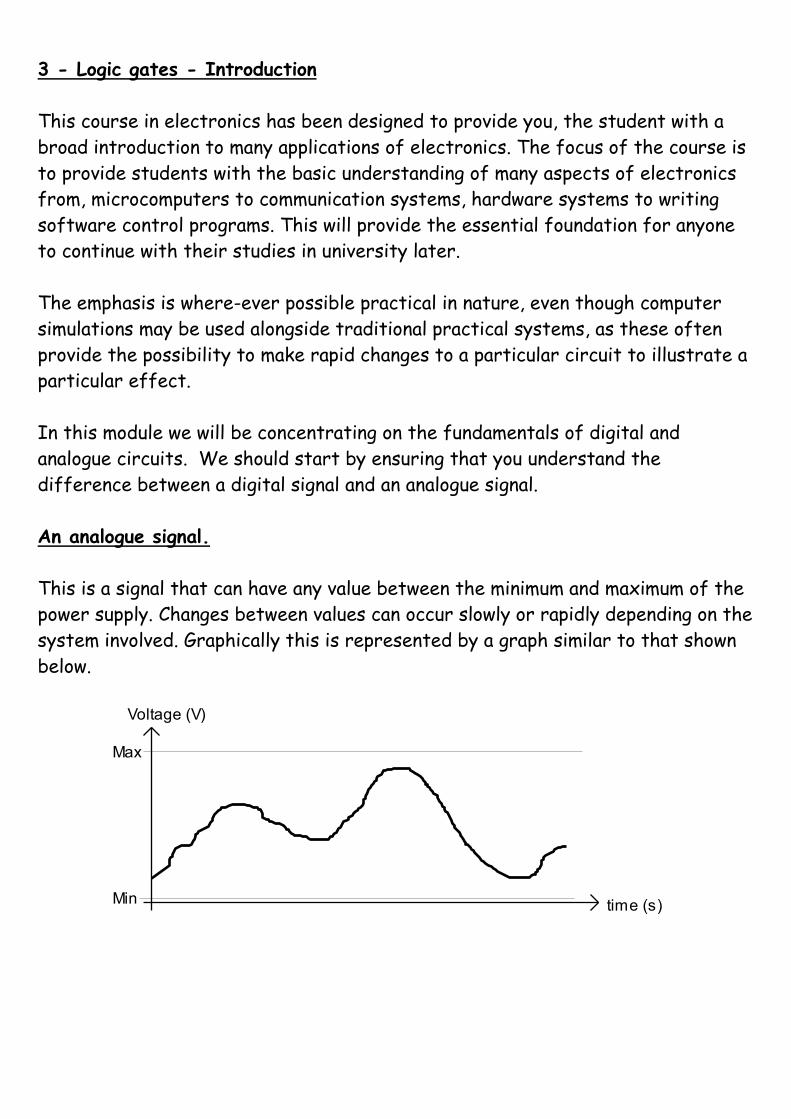
An analogue signal.
This is a signal that can have any value between the minimum and maximum of the
power supply. Changes between values can occur slowly or rapidly depending on the
system involved. Graphically this is represented by a graph similar to that shown
below.
Voltage (V)
time (s)
Max
Min
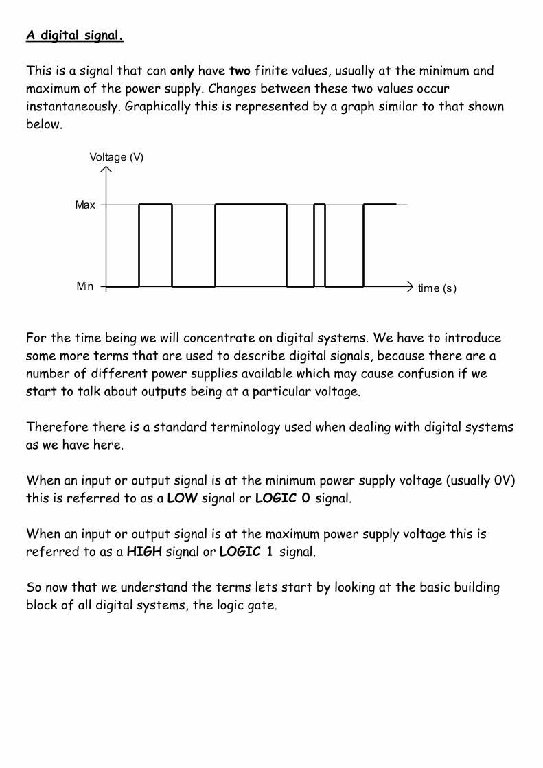
A digital signal.
This is a signal that can only have two finite values, usually at the minimum and
maximum of the power supply. Changes between these two values occur
instantaneously. Graphically this is represented by a graph similar to that shown
below.
For the time being we will concentrate on digital systems. We have to introduce
some more terms that are used to describe digital signals, because there are a
number of different power supplies available which may cause confusion if we
start to talk about outputs being at a particular voltage.
Therefore there is a standard terminology used when dealing with digital systems
as we have here.
When an input or output signal is at the minimum power supply voltage (usually 0V)
this is referred to as a LOW signal or LOGIC 0 signal.
When an input or output signal is at the maximum power supply voltage this is
referred to as a HIGH signal or LOGIC 1 signal.
So now that we understand the terms lets start by looking at the basic building
block of all digital systems, the logic gate.
Voltage (V)
time (s)
Max
Min

Logic Gates.
The term logic gate actually gives a clue as to the function of these devices in an
electronic circuit. ‘Logic’ implies some sort of rational thought process taking
place and a ‘gate’ in everyday language allows something through when it is opened.
A Logic Gate in an electronic sense makes a ‘logical’ decision based upon a set of
rules, and if the appropriate conditions are met then the gate is opened and an
output signal is produced.
Logic gates are therefore the decision making units in electronic systems and
there are many different types for different applications. We will now spend
some time looking at the different type of gates and the rules each one uses to
decide an appropriate output.
1. Look at the following logic symbols labelled A – G.
i. Which is the correct symbol for an AND gate. ……………
ii. Which is the correct symbol for a NOT gate. ……………
iii. Which is the correct symbol for a NOR gate. ……………
iv. Which is the correct symbol for an EXOR gate. ……………
v. Which is the correct symbol for a NAND gate. ……………
vi. Which is the correct symbol for an XNOR gate. ……………
vii. Which is the correct symbol for an OR gate. ……………

2. Complete the following truth tables.
i. AND gate.
Inputs Output B A Q
0 0
0 1
1 0
1 1
ii. NOR gate.
Inputs Output B A Q
0 0
0 1
1 0
1 1
iii. XNOR gate.
Inputs Output B A Q
0 0
0 1
1 0
1 1
iv. NAND gate.
Inputs Output B A Q
0 0
0 1
1 0
1 1

v. OR gate.
Inputs Output B A Q
0 0
0 1
1 0
1 1
3. The Boolean equations labelled A – I, below are to be used to answer the
following questions.
A) BAQ .
B) BAQ
C) BAQ
D) BABAQ ..
E) BAQ
F) BABAQ ..
G) AQ
H) BAQ .
I) BAQ
i. Which expression is correct for an AND gate. ……………
ii. Which expression is correct for a NOT gate. ……………
iii. Which expression is correct for a NOR gate. ……………
iv. Which two expressions are correct for an EXOR gate. ……… & ………
v. Which expression is correct for a NAND gate. ……………
vi. Which two expressions are correct for an XNOR gate. ……… & ………
vii. Which expression is correct for an OR gate. ……………

Task 4 - TURNING COMPUTING INSIDE OUT – COMPREHENSION EXERCISE
1. How does the author compare the cost of running the processor with cooling it?
2. What is running a “wimpy mode”
3. What is DRAM?
4. How long does it take for data to transfer from the disk to arrive in memory?
5. What is suggested as the current processor speed? How does this compare with your answer to (4)? Comment?
6. What is NAND?
7. What is a Memristor and how does it work?
8. What method did Sun Microsystems use to speed up 3D graphics?
9. Explain clearly what is meant by;
“It provides a completely new computer architecture that breaks the mould of von Neumann computing.”
10. Why bother with building a IkW supercomputer rather than a 1MW one?

Computing components: turning architectures inside-out
23 April 2012 By Chris Edwards Share |
We're all fed-up with watching the 'Please wait' icon as our data shunts backwards and
forwards from memory to processor... but could the waiting time be reduced now that
memory technology innovation is providing the key to a new, more energy-efficient way of
handling data?
When he got up on stage at the Intel Developer Forum last year, the head of the world's largest chipmaker
boasted of what his industry had achieved. Chief executive Paul Otellini described what had happened to
integrated circuits such as those inside the x86 processors in just ten years.
"The net result of all these innovations over the past decade has been astounding," Otellini claimed. "Over a
60-fold improvement in server performance powering the data centres, over a 30-times increase in client
performance at one-half the energy consumption."
This is progress; but it's still not enough.That is because solid progress is rarely enough in computing
componentry, because as soon as one part of a system is improved, another part seizes upon it. In this case
software has consumed these advances and drives the processors harder to the extent that cooling data
centres costs more than running the processors themselves. A new wave in supercomputing research is to
ease-off on individual processor speed and simply use many more of them.
In research presented first at the 22nd ACM Symposium of Operating Systems Principles in 2009, a team
from Carnegie- Mellon University and Intel Labs concluded that future compute servers for large data centres
should use simple embedded processors similar to and build them into huge arrays of, as they put it, "wimpy
nodes".
The result was a cluster that achieved 300 queries per joule, which the researchers claimed as being two
orders of magnitude better than traditional disk-based clusters. HP Labs achieved similar results with the
'microblade' server developed as a predecessor to its Project Moonshot – a data-warehouse architecture
made of simple, low-power processors.
"We explored the idea of using the same processors as those in smartphones. If you need ten thousand x86
processors you probably need millions of these," HP Labs director Prith Banerjee said at the DesignCon
conference in California at the end of January 2012. "How do you connect them? That is what we did with
Project Moonshot. That is our solution to the world."
Data transit speeds
One reason why large arrays of wimpy nodes are going to be important is that high-performance computing
is changing, Banerjee continued: "Data centres used to be targeted for lots of compute power. Now people
are doing lots of social networking and accessing lots of unstructured data. They need to access terabytes of
data very quickly."
Anyone who has been obliged to watch the never-empty Microsoft Windows hourglass, or the OS X
beachball spin, while their computer deals with more important things than its user, has experienced the
problem of having more data than will fit into main memory, normally dynamic random access memory
(DRAM). When a processor demands data from a disk drive it has to wait... And wait... And wait... And wait a
bit more.
It takes, on average, 10ms for the data from a disk to arrive in main memory after the software running on a
processor requests it. That does not sound long, but in practical terms it's forever for a processor that is
capable of crunching through as many as four instructions every third of a picosecond; and while it is waiting,
said processor's transistors are, in effect (or in non-effect, to be precise) busy doing nothing.
Then there is also the issue of energy leakage. Server-class processors lose a lot of energy just through
current that leaks into the silicon substrate, its energy ultimately dissipated as heat.
Many supercomputer applications can work around these problems by loading their data into memory first
and then crunching it - this works as long as you do not have too much data to begin with; but some
applications revolve around mining huge data libraries looking for patterns and these libraries cannot fit into
even the large quantities of DRAM found in supercomputers.
Flash's limitations
Cyberinfrastruncture specialist the San Diego Supercomputer Center, for example, designed its Gordon
supercomputer to handle these data-mining applications, using flash memory instead of rotating disks to
massively cut down the time waiting for data.
Flash has been surging ahead in capacity in recent years and at a rate that has, at least for a while,
surpassed Moore's Law. Eli Harari, former head of Sandisk, claimed at the International Solid State Circuits
Conference in February 2012 that it could prove cheaper than rotating disk drives by the end of the decade.
Part of the reason for the rapid fall in cost per gigabyte is down to the way that the most common form of
flash works. Manufacturers usually try to limit the die size of chips because yield typically falls as chips get
bigger, simply because the probability of them having failed cells increases dramatically. The NAND form of

flash found in SSDs is a little different and so, die size has in the past decade shot up compared to more
established memories such as DRAM.
Mike Bryant, chief technology officer at Future Horizons, explains: "You can make them as big as you want,
at least up to a point, and then use the memory controller to find the bad bits. A third of the bits could have
failed but the chip is still usable."
Another factor in favour of NAND flash is that the cells can store more than one bit: the controller can detect
small differences in charge that can be used to encode the four states needed for a 2bit memory cell. And
the industry is set to make a further step, encoding eight possible states to create a 3bit cell. Bill McClean,
head of IC Insights, says: "Most of the market for NAND is at least 2bit per cell. When we use 3bit per cell it
will really reduce the cost."
It is not all good news for flash. Reads are fast, but writes are more problematic. To save on expensive wiring
to the memory cells, it is only possible to erase complete blocks and then rewrite the contents even if you
only need to alter a single bit. This takes time.
A further problem is that flash wears out and, because of the trend to pack more data into each cell, average
cell endurance is dropping like a stone. "With 3bit-per-cell flash you get more errors and endurance goes
down. You may only get 1,000 write cycles," adds McClean.
Flash versus Anobit
Meanwhile, Apple is attempting to overcome these problems through the purchase of Israeli start-up Anobit,
which uses signal-processing techniques to improve the readability of the stored bits, says McClean: "Apple
paid a lot of money for Anobit, but Apple expects Anobit to get them up to 40,000 to 50,000 cycles with that
technology."
To avoid wearing blocks out, almost all flash controllers use a strategy called wear-levelling in which new,
empty blocks are remapped dynamically into place. The used, 'dirty' blocks are kept in reserve as long as
possible and only erased and rewritten once the supply of new blocks dries up. This has a knock-on effect on
performance.
When the drive gets dirty, it slows down because it has to stop and perform the erase when the new data
turns up, blocking other transfers. This works well in laptops, but is far from ideal in I/O intensive database
servers.
Wear-levelling uses up free blocks quickly and the drive is limited to the speed at which it can erase and
rewrite memory. The secret, as SSD makers have found, is to proactively erase blocks and make them
available before the OS calls for them.
The TRIM strategy used by Windows 7 uses this approach and drive vendors have built background-erase
routines into their hardware. Another player in this technology, Plextor, calls this strategy used in its solid
state drives 'Instant Restore'.
Other memory options
Other forms of memory are coming to the rescue. Dell and LSI are putting magnetoresistive random-access
memory (MRAM), developed by Everspin Technologies into their storage systems. MRAM is nowhere near
as cheap as flash, but writes to it are instant, so the storage companies are using it to cache data in case a
power cut stops the messages being written out to either disk drives or SSDs.

As software applications are reworked to take advantage of massive amounts of distributed main memory,
the next stage is to lose the bottleneck that remains between the processor and the memory.
According to analysis performed at Stanford University and other institutions, close to 40 per cent of the
power consumed by a processor is due to the act of fetching instructions from main memory – not counting
energy to process them or fetch data.
Most of that energy is lost in the electrical buses that connect the two; but massive savings could be made if
you did not have to move data so far. As Professor Gerhard Fettweis, of Dresden Technical University,
explained at the Design and Test in Europe conference in March 2012, it is now about working caches
smarter not harder: "The future will not be about making the processor cache larger, but seeing how we can
get computing into the memories." Doing that means turning computing inside out: discard the von Neumann
machine take processing to the data instead of vice versa.
"We have to rethink software architectures on the large scale," according to Fettweis's colleague at Dresden
Technical University, Professor Wolfgang Lehner.
One of the first steps to putting computing inside memory chips was the 3DRAM developed by electronics
giant Mitsubishi – now part of Renesas Technology – and Sun Microsystems in the mid-1990s. This
combined memory with tiny computing elements designed to speed-up 3D graphics by working out whether
one pixel was in front of another, and so should be rendered instead of forcing an external processor to read
out the pixel values and then write back the correct one.
More recently, US start-up Tabula developed an architecture that uses programmable circuitry to switch
computing elements in and out dynamically next to the where the data is stored.
"We are trying to look 20 years ahead with this architecture," claims the company's founder and CTO Steve
Teig. However, overturning the von Neumann hegemony is taking time. The programmable-logic market is
notoriously difficult to break into, dominated as it is by two major players: Altera and Xilinx. It's reasonable to
suggest that 3DRAM itself was a short-lived success.
It was launched at a time when cost dominated design decisions and was out-competed by conventional
memories and high-speed graphics processors and even prime customer Sun stopped using 3DRAM after
just a few years.
Memory merge splurge
The switch may come when the logic and memory elements themselves merge. Magnetic and spin-based
devices, such as those used in today's MRAMs, can potentially process data and store it in the one place.
Another promising technology is the memristor developed at HP Labs.
This device changes its resistance based on its stored state. Memristors can be made in dense crossbar
structures similar to conventional memories to form much more compact computers and even architectures
that begin to resemble the brain: another machine in which memory and processing are combined.
The inventor of the concept of the memristor, Professor Leon Chua of the University of California at Berkeley
claims that axons and synapses are effectively electrochemical memristors. "The brain is made of
memristors," Chua proposes.
"The memristor is completely different to what we had in the past. It can learn by itself; and it is why we will
see smart machines coming out in the next ten years that will be small – and truly intelligent."

Brain-like functionality
Dharmendra Modha, founding manager of the cognitive computing centre at IBM Almaden Research Labs, is
using similar techniques to simulate the behaviour of the billions of human synapses in a DARPA-funded
project to build a 1kW rather than 1MW supercomputer.
"We are equating the synapse with the bitline and wordline of a memory. We figured out how to implement
learning in an efficient way in this simple translation from biology to electronics," Modha explained at the
Design Automation Conference last year.
"It provides a completely new computer architecture that breaks the mould of von Neumann computing. We
found going through this project that when we were searching for brain-like function we were making no
progress. But the moment we brought in the need to design a low-power implementation, the very process of
incorporating technological constraints into our way of thinking led to a new direction."
Over the last three decades the computer industry has proved to be adept at restructuring its operations in
order to take advantage of innovations and (so-called) disruptive technologies. However, much of this
change has been refinements to existing technological models; much of the basic 'architecture' of computing
looks the same as it was when the IBM PC first shipped in the early 1980s.
The constraints that IBM's Modha has been describing could ultimately turn computing inside out and usher
in completely new, self-learning architectures. And memory lies at the core of this movement. *
Further information
www.intel.co.uk/
www.hpl.hp.com/
www.sandisk.com/
www.futurehorizons.com/
www.icinsights.com/
www.plextor.com/
www.everspin.com/
www.dell.co.uk/
www.lsi.com/
www.mitsubishielectric.com/semiconductors/
www.tabula.com/
www.almaden.ibm.com/