trenchstoptm th - infineon technologies
TRANSCRIPT
Datasheet PleasereadtheImportantNoticeandWarningsattheendofthisdocument V2.1www.infineon.com 2020-07-27
IKW75N65RH5
HybridCoolSiCTMIGBT
TRENCHSTOPTM5H5IGBTco-packedwithhalf-rated6thgenerationCoolSiCTMSchottkybarrierdiodeFeaturesandBenefits:
•Ultra-lowswitchinglossesduetothecombinationofTRENCHSTOPTM5andCoolSiCTMtechnology•Benchmarkefficiencyinhardswitchingtopologies•Plug-and-playreplacementofpuresilicondevices•Maximumjunctiontemperature175°C•QualifiedaccordingtoJEDECfortargetapplications•Pb-freeleadplating;RoHScompliant•CompleteproductspectrumandPSpicemodels:http://www.infineon.com/igbt/
PotentialApplications:
•IndustrialPowerSupplies-IndustrialSMPS-IndustrialUPS•EnergyGeneration-SolarStringInverter•EnergyDistribution-EnergyStorage•Infrastructure–Charge-Charger
ProductValidation:
QualifiedforapplicationslistedabovebasedonthetestconditionsintherelevanttestsofJEDEC20/22
Packagepindefinition:
•Pin1-gate•Pin2&backside-collector•Pin3-emitter
G
C
E
12
3
KeyPerformanceandPackageParametersType VCE IC VCEsat,Tvj=25°C Tvjmax Marking PackageIKW75N65RH5 650V 75A 1.65V 175°C K75ERH5 PG-TO247-3
Datasheet 2 V2.12020-07-27
IKW75N65RH5
HybridCoolSiCTMIGBT
TableofContents
Description . . . . . . . . . . . . . . . . . . . . . . . . . . . . . . . . . . . . . . . . . . . . . . . . . . . . . . . . . . . . . . . . . . . . . . . . 1
Table of Contents . . . . . . . . . . . . . . . . . . . . . . . . . . . . . . . . . . . . . . . . . . . . . . . . . . . . . . . . . . . . . . . . . . . 2
Maximum Ratings . . . . . . . . . . . . . . . . . . . . . . . . . . . . . . . . . . . . . . . . . . . . . . . . . . . . . . . . . . . . . . . . . . . 3
Thermal Resistance . . . . . . . . . . . . . . . . . . . . . . . . . . . . . . . . . . . . . . . . . . . . . . . . . . . . . . . . . . . . . . . . . 3
Electrical Characteristics . . . . . . . . . . . . . . . . . . . . . . . . . . . . . . . . . . . . . . . . . . . . . . . . . . . . . . . . . . . . . . 4
Electrical Characteristics Diagrams . . . . . . . . . . . . . . . . . . . . . . . . . . . . . . . . . . . . . . . . . . . . . . . . . . . . . 6
Package Drawing . . . . . . . . . . . . . . . . . . . . . . . . . . . . . . . . . . . . . . . . . . . . . . . . . . . . . . . . . . . . . . . . . . .12
Testing Conditions . . . . . . . . . . . . . . . . . . . . . . . . . . . . . . . . . . . . . . . . . . . . . . . . . . . . . . . . . . . . . . . . . .13
Revision History . . . . . . . . . . . . . . . . . . . . . . . . . . . . . . . . . . . . . . . . . . . . . . . . . . . . . . . . . . . . . . . . . . . .14
Disclaimer . . . . . . . . . . . . . . . . . . . . . . . . . . . . . . . . . . . . . . . . . . . . . . . . . . . . . . . . . . . . . . . . . . . . . . . . .15

Datasheet 3 V2.12020-07-27
IKW75N65RH5
HybridCoolSiCTMIGBT
MaximumRatingsForoptimumlifetimeandreliability,Infineonrecommendsoperatingconditionsthatdonotexceed80%ofthemaximumratingsstatedinthisdatasheet.
Parameter Symbol Value UnitCollector-emittervoltage,Tvj≥25°C VCE 650 V
DCcollectorcurrent,limitedbyTvjmaxTc=25°CvaluelimitedbybondwireTc=100°C
IC 80.075.0
A
Pulsedcollectorcurrent,tplimitedbyTvjmax ICpuls 300.0 A
Turn off safe operating areaVCE≤650V,Tvj≤175°C,tp=1µs - 300.0 A
Diodeforwardcurrent,limitedbyTvjmaxTc=25°CTc=100°C
IF 45.730.7
A
Diodepulsedcurrent,tplimitedbyTvjmax1) IFpuls 112.5 A
Gate-emitter voltageTransientGate-emittervoltage(tp≤10µs,D<0.010) VGE
±20±30 V
PowerdissipationTc=25°CPowerdissipationTc=100°C Ptot
395.0198.0 W
Operating junction temperature Tvj -40...+175 °C
Storage temperature Tstg -55...+150 °C
Soldering temperature,wave soldering 1.6mm (0.063in.) from case for 10s 260 °C
Mounting torque, M3 screwMaximum of mounting processes: 3 M 0.6 Nm
ThermalResistance
Valuemin. typ. max.
Parameter Symbol Conditions Unit
RthCharacteristics
IGBT thermal resistance,junction - case Rth(j-c) - - 0.38 K/W
Diode thermal resistance,junction - case Rth(j-c) - - 1.20 K/W
Thermal resistancejunction - ambient Rth(j-a) - - 40 K/W
1) Pulse current level depends on Tvj of diode chip, see also Fig. "Maximum pulse current as a function of junction temperature"

Datasheet 4 V2.12020-07-27
IKW75N65RH5
HybridCoolSiCTMIGBT
ElectricalCharacteristic,atTvj=25°C,unlessotherwisespecified
Valuemin. typ. max.
Parameter Symbol Conditions Unit
StaticCharacteristic
Collector-emitter saturation voltage VCEsat
VGE=15.0V,IC=75.0ATvj=25°CTvj=125°CTvj=175°C
---
1.651.851.95
2.10--
V
Diode forward voltage VF
VGE=0V,IF=30.0ATvj=25°CTvj=125°CTvj=175°C
---
1.351.551.65
1.50--
V
Gate-emitter threshold voltage VGE(th) IC=0.75mA,VCE=VGE 3.2 4.0 4.8 V
Zero gate voltage collector current ICESVCE=650V,VGE=0VTvj=25°CTvj=175°C
--
-2500
1000-
µA
Zero gate voltage collector current ICES VCE=480V,VGE=0VTvj=25°C - - 30 µA
Gate-emitter leakage current IGES VCE=0V,VGE=20V - - 100 nA
Transconductance gfs VCE=20V,IC=75.0A - 105.0 - S
ElectricalCharacteristic,atTvj=25°C,unlessotherwisespecified
Valuemin. typ. max.
Parameter Symbol Conditions Unit
DynamicCharacteristic
Input capacitance Cies - 4000 -
Output capacitance Coes - 460 -
Reverse transfer capacitance Cres - 15 -
VCE=25V,VGE=0Vf=250kHz pF
Gate charge QGVCC=520V,IC=75.0A,VGE=15V - 168.0 - nC
Internal emitter inductancemeasured 5mm (0.197 in.) fromcase
LE - 13.0 - nH
SwitchingCharacteristic,InductiveLoad
Valuemin. typ. max.
Parameter Symbol Conditions Unit
IGBTCharacteristic,atTvj=25°CTurn-on delay time td(on) - 26 - ns
Rise time tr - 9 - ns
Turn-off delay time td(off) - 180 - ns
Fall time tf - 15 - ns
Turn-on energy Eon - 0.36 - mJ
Turn-off energy Eoff - 0.30 - mJ
Total switching energy Ets - 0.66 - mJ
Tvj=25°C,VCC=400V,IC=37.5A,VGE=0.0/15.0V,RG(on)=9.0Ω,RG(off)=9.0Ω,Lσ=30nH,Cσ=30pFLσ,CσfromFig.EEnergy losses include “tail” anddiode reverse recovery.

Datasheet 5 V2.12020-07-27
IKW75N65RH5
HybridCoolSiCTMIGBT
Turn-on delay time td(on) - 26 - ns
Rise time tr - 3 - ns
Turn-off delay time td(off) - 220 - ns
Fall time tf - 35 - ns
Turn-on energy Eon - 0.07 - mJ
Turn-off energy Eoff - 0.08 - mJ
Total switching energy Ets - 0.15 - mJ
Tvj=25°C,VCC=400V,IC=7.5A,VGE=0.0/15.0V,RG(on)=9.0Ω,RG(off)=9.0Ω,Lσ=30nH,Cσ=30pFLσ,CσfromFig.EEnergy losses include “tail” anddiode reverse recovery.
SwitchingCharacteristic,InductiveLoad
Valuemin. typ. max.
Parameter Symbol Conditions Unit
IGBTCharacteristic,atTvj=150°CTurn-on delay time td(on) - 24 - ns
Rise time tr - 12 - ns
Turn-off delay time td(off) - 205 - ns
Fall time tf - 18 - ns
Turn-on energy Eon - 0.45 - mJ
Turn-off energy Eoff - 0.40 - mJ
Total switching energy Ets - 0.85 - mJ
Tvj=150°C,VCC=400V,IC=37.5A,VGE=0.0/15.0V,RG(on)=9.0Ω,RG(off)=9.0Ω,Lσ=30nH,Cσ=30pFLσ,CσfromFig.EEnergy losses include “tail” anddiode reverse recovery.
Turn-on delay time td(on) - 20 - ns
Rise time tr - 5 - ns
Turn-off delay time td(off) - 240 - ns
Fall time tf - 40 - ns
Turn-on energy Eon - 0.09 - mJ
Turn-off energy Eoff - 0.11 - mJ
Total switching energy Ets - 0.20 - mJ
Tvj=150°C,VCC=400V,IC=7.5A,VGE=0.0/15.0V,RG(on)=9.0Ω,RG(off)=9.0Ω,Lσ=30nH,Cσ=30pFLσ,CσfromFig.EEnergy losses include “tail” anddiode reverse recovery.
Datasheet 6 V2.12020-07-27
IKW75N65RH5
HybridCoolSiCTMIGBT
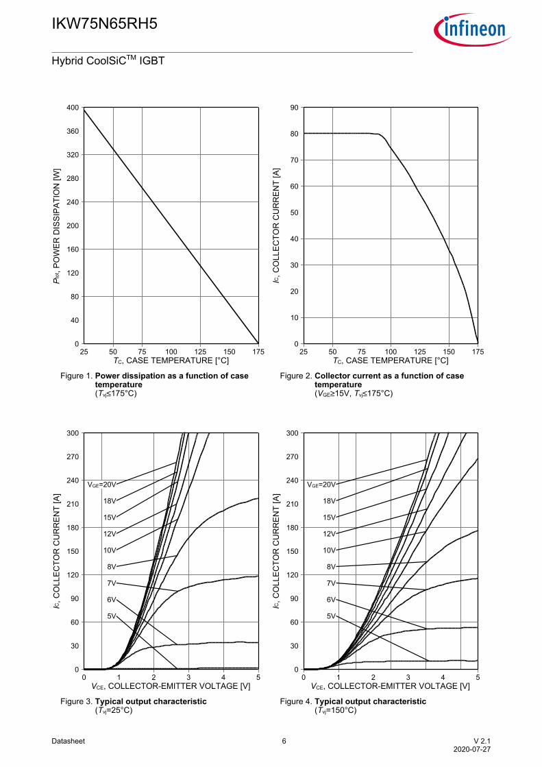
Figure 1. Powerdissipationasafunctionofcasetemperature(Tvj≤175°C)
TC,CASETEMPERATURE[°C]
Ptot ,PO
WER
DISSIPA
TION[W
]
25 50 75 100 125 150 1750
40
80
120
160
200
240
280
320
360
400
Figure 2. Collectorcurrentasafunctionofcasetemperature(VGE≥15V,Tvj≤175°C)
TC,CASETEMPERATURE[°C]
IC,C
OLLEC
TORCURREN
T[A]
25 50 75 100 125 150 1750
10
20
30
40
50
60
70
80
90
Figure 3. Typicaloutputcharacteristic(Tvj=25°C)
VCE,COLLECTOR-EMITTERVOLTAGE[V]
IC,C
OLLEC
TORCURREN
T[A]
0 1 2 3 4 50
30
60
90
120
150
180
210
240
270
300
VGE=20V
18V
15V
12V
10V
8V
7V
6V
5V
Figure 4. Typicaloutputcharacteristic(Tvj=150°C)
VCE,COLLECTOR-EMITTERVOLTAGE[V]
IC,C
OLLEC
TORCURREN
T[A]
0 1 2 3 4 50
30
60
90
120
150
180
210
240
270
300
VGE=20V
18V
15V
12V
10V
8V
7V
6V
5V

Datasheet 7 V2.12020-07-27
IKW75N65RH5
HybridCoolSiCTMIGBT
Figure 5. Typicaltransfercharacteristic(VCE=20V)
VGE,GATE-EMITTERVOLTAGE[V]
IC,C
OLLEC
TORCURREN
T[A]
2.5 3.5 4.5 5.5 6.5 7.5 8.5 9.50
30
60
90
120
150
180
210
240
270
300Tj=25°CTj=150°C
Figure 6. Typicalcollector-emittersaturationvoltageasafunctionofjunctiontemperature(VGE=15V)
Tvj,JUNCTIONTEMPERATURE[°C]
VCEsat,C
OLLEC
TOR-EMITTE
RSAT
URAT
ION[V
]
25 50 75 100 125 150 1750.50
0.75
1.00
1.25
1.50
1.75
2.00
2.25
2.50IC=18.75AIC=37.5AIC=75A
Figure 7. Typicalswitchingtimesasafunctionofcollectorcurrent(inductiveload,Tvj=150°C,VCE=400V,VGE=15/0V,RG=9Ω,DynamictestcircuitinFigure E)
IC,COLLECTORCURRENT[A]
t,SW
ITCHINGTIMES
[ns]
0 25 50 75 100 125 150 175 200 2251
10
100
1000td(off)
tftd(on)
tr
Figure 8. Typicalswitchingtimesasafunctionofgateresistor(inductiveload,Tvj=150°C,VCE=400V,VGE=15/0V,IC=37.5A,DynamictestcircuitinFigure E)
RG,GATERESISTOR[Ω]
t,SW
ITCHINGTIMES
[ns]
0 5 10 15 20 25 30 35 401
10
100
1000td(off)
tftd(on)
tr

Datasheet 8 V2.12020-07-27
IKW75N65RH5
HybridCoolSiCTMIGBT
Figure 9. Typicalswitchingtimesasafunctionofjunctiontemperature(inductiveload,VCE=400V,VGE=15/0V,IC=37.5A,RG=9Ω,DynamictestcircuitinFigure E)
Tvj,JUNCTIONTEMPERATURE[°C]
t,SW
ITCHINGTIMES
[ns]
25 50 75 100 125 150 1751
10
100
1000td(off)
tftd(on)
tr
Figure 10. Gate-emitterthresholdvoltageasafunctionofjunctiontemperature(IC=0.75mA)
Tvj,JUNCTIONTEMPERATURE[°C]
VGE(th) ,GAT
E-EM
ITTE
RTHRES
HOLD
VOLTAG
E[V]
25 50 75 100 125 1501.0
1.5
2.0
2.5
3.0
3.5
4.0
4.5
5.0
5.5typ.
Figure 11. Typicalswitchingenergylossesasafunctionofcollectorcurrent(inductiveload,Tvj=150°C,VCE=400V,VGE=15/0V,RG=9Ω,DynamictestcircuitinFigure E)
IC,COLLECTORCURRENT[A]
E,S
WITCHINGENER
GYLO
SSES
[mJ]
0 25 50 75 100 125 150 175 200 2250
2
4
6
8
10
12
14Eoff
Eon
Ets
Figure 12. Typicalswitchingenergylossesasafunctionofgateresistor(inductiveload,Tvj=150°C,VCE=400V,VGE=15/0V,IC=37.5A,DynamictestcircuitinFigure E)
RG,GATERESISTOR[Ω]
E,S
WITCHINGENER
GYLO
SSES
[mJ]
0 5 10 15 20 25 30 35 400.00
0.25
0.50
0.75
1.00
1.25
1.50
1.75
2.00
2.25
2.50Eoff
Eon
Ets
Datasheet 9 V2.12020-07-27
IKW75N65RH5
HybridCoolSiCTMIGBT
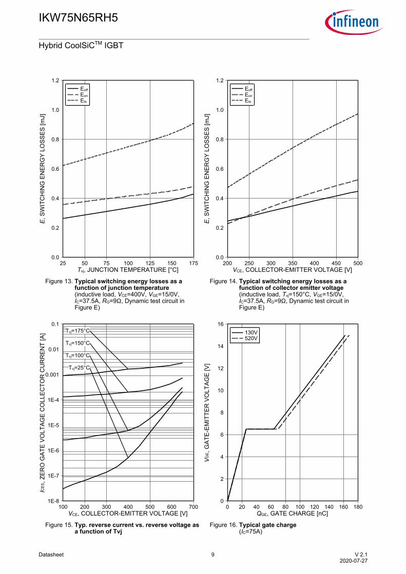
Figure 13. Typicalswitchingenergylossesasafunctionofjunctiontemperature(inductiveload,VCE=400V,VGE=15/0V,IC=37.5A,RG=9Ω,DynamictestcircuitinFigure E)
Tvj,JUNCTIONTEMPERATURE[°C]
E,S
WITCHINGENER
GYLO
SSES
[mJ]
25 50 75 100 125 150 1750.0
0.2
0.4
0.6
0.8
1.0
1.2Eoff
Eon
Ets
Figure 14. Typicalswitchingenergylossesasafunctionofcollectoremittervoltage(inductiveload,Tvj=150°C,VGE=15/0V,IC=37.5A,RG=9Ω,DynamictestcircuitinFigure E)
VCE,COLLECTOR-EMITTERVOLTAGE[V]
E,S
WITCHINGENER
GYLO
SSES
[mJ]
200 250 300 350 400 450 5000.0
0.2
0.4
0.6
0.8
1.0
1.2Eoff
Eon
Ets
Figure 15. Typ.reversecurrentvs.reversevoltageasafunctionofTvj
VCE,COLLECTOR-EMITTERVOLTAGE[V]
ICES,ZER
OGAT
EVO
LTAG
ECOLLEC
TORCURREN
T[A]
100 200 300 400 500 600 7001E-8
1E-7
1E-6
1E-5
1E-4
0.001
0.01
0.1Tvj=175°C
Tvj=150°C
Tvj=100°C
Tvj=25°C
Figure 16. Typicalgatecharge(IC=75A)
QGE,GATECHARGE[nC]
VGE ,GAT
E-EM
ITTE
RVOLTAG
E[V]
0 20 40 60 80 100 120 140 160 1800
2
4
6
8
10
12
14
16130V520V

Datasheet 10 V2.12020-07-27
IKW75N65RH5
HybridCoolSiCTMIGBT
Figure 17. Typicalcapacitanceasafunctionofcollector-emittervoltage(VGE=0V,f=250kHz)
VCE,COLLECTOR-EMITTERVOLTAGE[V]
C,C
APAC
ITAN
CE[pF]
0 5 10 15 20 25 301
10
100
1000
1E+4Cies
Coes
Cres
Figure 18. IGBTtransientthermalresistance(D=tp/T)
tp,PULSEWIDTH[s]
Zth(j -c
) ,TR
ANSIEN
TTH
ERMAL
RES
ISTA
NCE[K/W
]
1E-6 1E-5 1E-4 0.001 0.01 0.1 10.001
0.01
0.1D=0.5
0.2
0.1
0.05
0.02
0.01
single pulse
i:ri[K/W]:τi[s]:
10.036770995.2E-5
20.034689953.7E-4
30.0336813.7E-4
40.0878943.3E-3
50.0855040.021173
60.101460.107752
Figure 19. Diodetransientthermalimpedanceasafunctionofpulsewidth(D=tp/T)
tp,PULSEWIDTH[s]
Zth(j -c
) ,TR
ANSIEN
TTH
ERMAL
RES
ISTA
NCE[K/W
]
1E-6 1E-5 1E-4 0.001 0.01 0.1 10.001
0.01
0.1
1
D=0.5
0.2
0.1
0.05
0.02
0.01
single pulse
i:ri[K/W]:τi[s]:
10.3861013.6E-4
20.4800292.4E-3
30.333870.01997
Figure 20. Maximumpulsecurrentasafunctionofjunctiontemperature
Tvj,JUNCTIONTEMPERATURE[°C]
IFpuls ,DIODEPU
LSED
CURREN
T[A]
25 50 75 100 125 150 1750
50
100
150
200
250
300
350

Datasheet 11 V2.12020-07-27
IKW75N65RH5
HybridCoolSiCTMIGBT
Figure 21. Typicaldiodeforwardcurrentasafunctionofforwardvoltage
VF,FORWARDVOLTAGE[V]
IF ,FORWAR
DCURREN
T[A]
0.0 0.5 1.0 1.5 2.0 2.5 3.0 3.5 4.00
20
40
60
80
100
120Tj=25°CTj=150°C
Figure 22. Typicaldiodeforwardvoltageasafunctionofjunctiontemperature
Tvj,JUNCTIONTEMPERATURE[°C]
VF ,FO
RWAR
DVOLTAG
E[V]
25 50 75 100 125 150 1750.0
0.5
1.0
1.5
2.0
2.5
3.0IF=15AIF=30AIF=60A

Datasheet 12 V2.12020-07-27
IKW75N65RH5
HybridCoolSiCTMIGBT
MILLIMETERS
5.44
c
Q
E3
E2
D
E
D1
D2
L1
e
L
S
P
E1
b1
A
A1
b
A2
b2
0.38
6.04
5.35
1.00
3.40
3.85
20.70
13.08
15.50
0.51
3.50
19.80
12.38
1.60
4.70
2.20
1.00
1.50
2.57
0.89
6.30
6.25
17.65
2.60
5.10
14.15
3.70
21.50
16.30
20.40
1.35
4.50
2.41
5.30
2.60
1.40
2.50
3.43
1
REVISION
06
25.07.2018
ISSUE DATE
EUROPEAN PROJECTION
0
SCALE
5mm
DOCUMENT NO.
Z8B00003327
DIMENSIONSMIN. MAX.
3:1
2 3 4
Package Drawing PG-TO247-3

Datasheet 13 V2.12020-07-27
IKW75N65RH5
HybridCoolSiCTMIGBT
t
a b
td(off)
tf t
rtd(on)
90% IC
10% IC
90% IC
10% VGE
10% IC
t
90% VGE
t
t
90% VGE
VGE
(t)
t
t
tt1 t
4
2% IC
10% VGE
2% VCE
t2
t3
E
t
t
V I toff
= x x d
1
2
CE CE
t
t
V I ton
= x x d
3
4
CE C
CC
dI /dtF
dI
I,V
Figure A.
Figure B.
Figure C. Definition of diode switchingcharacteristics
Figure E. Dynamic test circuit
Figure D.
I (t)C
Parasitic inductance L ,
parasitic capacitor C ,
relief capacitor C ,
(only for ZVT switching)
s
s
r
t t t
Q Q Qrr a b
rr a b
= +
= +
Qa Qb
V (t)CE
VGE
(t)
I (t)C
V (t)CE
Testing Conditions
Datasheet 14 V2.12020-07-27
IKW75N65RH5
HybridCoolSiCTMIGBT
RevisionHistory
IKW75N65RH5
Revision:2020-07-27,Rev.2.1Previous Revision
Revision Date Subjects (major changes since last revision)
1.1 2020-03-20 Preliminary Data Sheet
2.1 2020-07-27 Final Data Sheet
Trademarks
Allreferencedproductorservicenamesandtrademarksarethepropertyoftheirrespectiveowners.
PublishedbyInfineonTechnologiesAG81726München,Germany©InfineonTechnologiesAG2020.AllRightsReserved.
ImportantNoticeTheinformationgiveninthisdocumentshallinnoeventberegardedasaguaranteeofconditionsorcharacteristics(“Beschaffenheitsgarantie”).Withrespecttoanyexamples,hintsoranytypicalvaluesstatedhereinand/oranyinformationregardingtheapplicationoftheproduct,InfineonTechnologiesherebydisclaimsanyandallwarrantiesandliabilitiesofanykind,includingwithoutlimitationwarrantiesofnon-infringementofintellectualpropertyrightsofanythirdparty.
Inaddition,anyinformationgiveninthisdocumentissubjecttocustomer’scompliancewithitsobligationsstatedinthisdocumentandanyapplicablelegalrequirements,normsandstandardsconcerningcustomer’sproductsandanyuseoftheproductofInfineonTechnologiesincustomer’sapplications.
Thedatacontainedinthisdocumentisexclusivelyintendedfortechnicallytrainedstaff.Itistheresponsibilityofcustomer’stechnicaldepartmentstoevaluatethesuitabilityoftheproductfortheintendedapplicationandthecompletenessoftheproductinformationgiveninthisdocumentwithrespecttosuchapplication.
Forfurtherinformationontheproduct,technology,deliverytermsandconditionsandpricespleasecontactyournearestInfineonTechnologiesoffice(www.infineon.com).
PleasenotethatthisproductisnotqualifiedaccordingtotheAECQ100orAECQ101documentsoftheAutomotiveElectronicsCouncil.
WarningsDuetotechnicalrequirementsproductsmaycontaindangeroussubstances.ForinformationonthetypesinquestionpleasecontactyournearestInfineonTechnologiesoffice.
ExceptasotherwiseexplicitlyapprovedbyInfineonTechnologiesinawrittendocumentsignedbyauthorizedrepresentativesofInfineonTechnologies,InfineonTechnologies’productsmaynotbeusedinanyapplicationswhereafailureoftheproductoranyconsequencesoftheusethereofcanreasonablybeexpectedtoresultinpersonalinjury.