trf3703 quadrature modulator evm (rev. b · pdf file3 gsm edge evm at 1800 mhz ... 6 trf3703...
TRANSCRIPT
TRF3703 Quadrature Modulator EvaluationModule
User's Guide
Literature Number: SLWU042BOctober 2006–Revised August 2008

2 SLWU042B–October 2006–Revised August 2008Submit Documentation Feedback
Contents
1 Overview ............................................................................................................................ 51.1 Purpose..................................................................................................................... 51.2 EVM Circuit Overview .................................................................................................... 51.3 Power Requirements ..................................................................................................... 51.4 TRF3703 EVM Operating Procedure................................................................................... 6
2 Physical Description ........................................................................................................... 112.1 PCB Layout............................................................................................................... 112.2 Parts List.................................................................................................................. 18
3 Circuit Description.............................................................................................................. 183.1 Circuit Function .......................................................................................................... 18
4 Circuit Board ..................................................................................................................... 195 Schematic ......................................................................................................................... 20
Important Notices ............................................................................................................... 21
SLWU042B–October 2006–Revised August 2008 Table of Contents 3Submit Documentation Feedback
www.ti.com
List of Figures1 Un-Optimized Sideband Suppression..................................................................................... 72 Optimized Sideband Suppression ......................................................................................... 83 GSM EDGE EVM at 1800 MHz............................................................................................ 94 1.5-V Interface Network for 19.2 mA Full Scale........................................................................ 105 3.3-V Interface Network for 19.2 mA Full Scale........................................................................ 106 Top Layer.................................................................................................................... 117 Top Layer–NH .............................................................................................................. 128 Ground Plane L2 ........................................................................................................... 139 Ground Plane L3 ........................................................................................................... 1410 Layer 4—Bottom Layer .................................................................................................... 1511 Layer 4—Bottom Layer–NH............................................................................................... 1612 Drill Pattern.................................................................................................................. 1713 Silkscreen Top Layer ...................................................................................................... 1914 TRF3703 EVM Schematic ................................................................................................ 20
List of Tables1 Bill of Materials for TRF3703 EVM....................................................................................... 182 Power Supply J1 ........................................................................................................... 18
4 List of Figures SLWU042B–October 2006–Revised August 2008Submit Documentation Feedback
1 Overview
1.1 Purpose
1.2 EVM Circuit Overview
1.3 Power Requirements
User's GuideSLWU042B–October 2006–Revised August 2008
TRF3703 Quadrature Modulator Evaluation Module
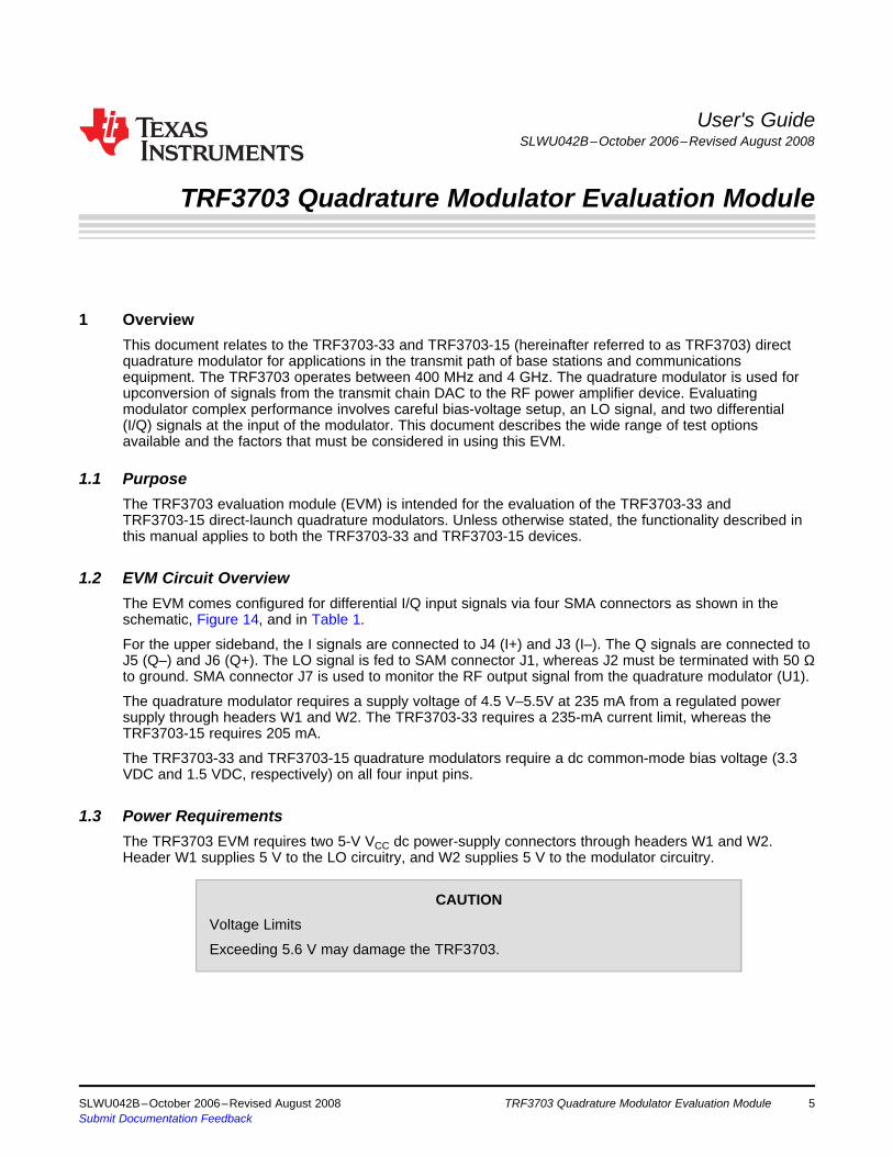
This document relates to the TRF3703-33 and TRF3703-15 (hereinafter referred to as TRF3703) directquadrature modulator for applications in the transmit path of base stations and communicationsequipment. The TRF3703 operates between 400 MHz and 4 GHz. The quadrature modulator is used forupconversion of signals from the transmit chain DAC to the RF power amplifier device. Evaluatingmodulator complex performance involves careful bias-voltage setup, an LO signal, and two differential(I/Q) signals at the input of the modulator. This document describes the wide range of test optionsavailable and the factors that must be considered in using this EVM.
The TRF3703 evaluation module (EVM) is intended for the evaluation of the TRF3703-33 andTRF3703-15 direct-launch quadrature modulators. Unless otherwise stated, the functionality described inthis manual applies to both the TRF3703-33 and TRF3703-15 devices.
The EVM comes configured for differential I/Q input signals via four SMA connectors as shown in theschematic, Figure 14, and in Table 1.
For the upper sideband, the I signals are connected to J4 (I+) and J3 (I–). The Q signals are connected toJ5 (Q–) and J6 (Q+). The LO signal is fed to SAM connector J1, whereas J2 must be terminated with 50 Ωto ground. SMA connector J7 is used to monitor the RF output signal from the quadrature modulator (U1).
The quadrature modulator requires a supply voltage of 4.5 V–5.5V at 235 mA from a regulated powersupply through headers W1 and W2. The TRF3703-33 requires a 235-mA current limit, whereas theTRF3703-15 requires 205 mA.
The TRF3703-33 and TRF3703-15 quadrature modulators require a dc common-mode bias voltage (3.3VDC and 1.5 VDC, respectively) on all four input pins.
The TRF3703 EVM requires two 5-V VCC dc power-supply connectors through headers W1 and W2.Header W1 supplies 5 V to the LO circuitry, and W2 supplies 5 V to the modulator circuitry.
CAUTIONVoltage Limits
Exceeding 5.6 V may damage the TRF3703.
SLWU042B–October 2006–Revised August 2008 TRF3703 Quadrature Modulator Evaluation Module 5Submit Documentation Feedback
1.4 TRF3703 EVM Operating Procedure
1.4.1 Typical Test Results
1.4.1.1 Un-Optimized Sideband Suppression
Overview www.ti.com
Set up the EVM as follows:1. Power-supply connection:
a. Switch on the VCC (5-V) supply and set the current limit set to 235 mA.b. Connect the 5-V supply to headers W1 and W2.c. Verify that the current drawn is approximately ≤ 205 mA for the TRF3703-15 and ≤ 235 mA for the
TRF3703-33.2. Use a suitable 50-Ω output signal generator (LO = ±5 dBm) or the TRF3761 to supply the LO signal at
desired frequency to J1, and terminate J2 with 50 Ω to ground.3. Use a DAC or an arbitrary waveform generator to provide the I/Q input signals. A typical setup is as
follows: a 1-Vp-p sine wave, a frequency of 50 KHz, a dc-offset of 0 V, and an output impedance of50 Ω (typically an ESG vector signal generator or similar).
4. Set the common mode on the ESG to either 1.65 V or 0.75 V, depending on device type (set to 1.65 Vfor the TRF3703-33, set to 0.75 V for the TRF3703-15).
5. Use an arbitrary waveform generator to suppress the sideband. Adjust the I/Q amplitude and phase ofthe CW signal coming from the arbitrary waveform generator.
6. Connect a spectrum analyzer to the SMA connector marked RFOUT (J7) and monitor the TRF3703output.
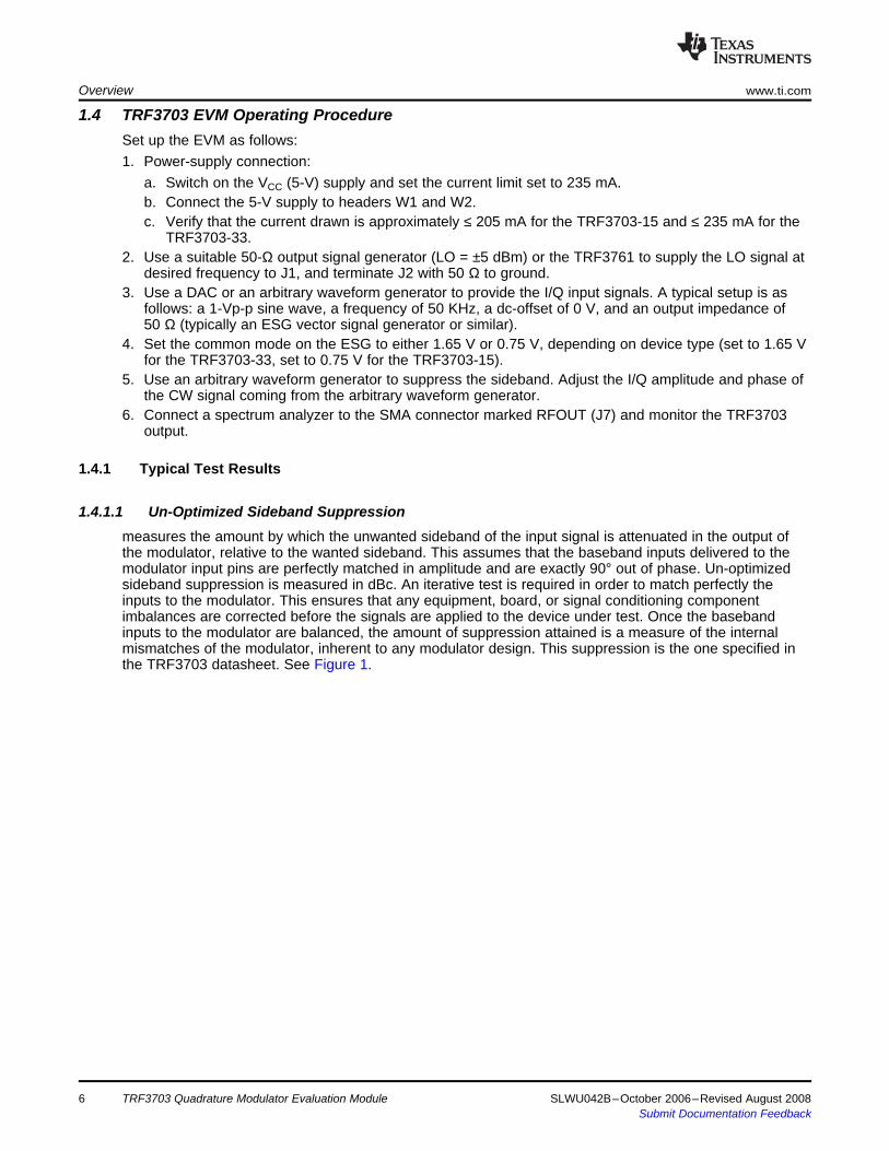
measures the amount by which the unwanted sideband of the input signal is attenuated in the output ofthe modulator, relative to the wanted sideband. This assumes that the baseband inputs delivered to themodulator input pins are perfectly matched in amplitude and are exactly 90° out of phase. Un-optimizedsideband suppression is measured in dBc. An iterative test is required in order to match perfectly theinputs to the modulator. This ensures that any equipment, board, or signal conditioning componentimbalances are corrected before the signals are applied to the device under test. Once the basebandinputs to the modulator are balanced, the amount of suppression attained is a measure of the internalmismatches of the modulator, inherent to any modulator design. This suppression is the one specified inthe TRF3703 datasheet. See Figure 1.
6 TRF3703 Quadrature Modulator Evaluation Module SLWU042B–October 2006–Revised August 2008Submit Documentation Feedback
C003
1.4.1.2 Optimized Sideband Suppression
www.ti.com Overview
Figure 1. Un-Optimized Sideband Suppression
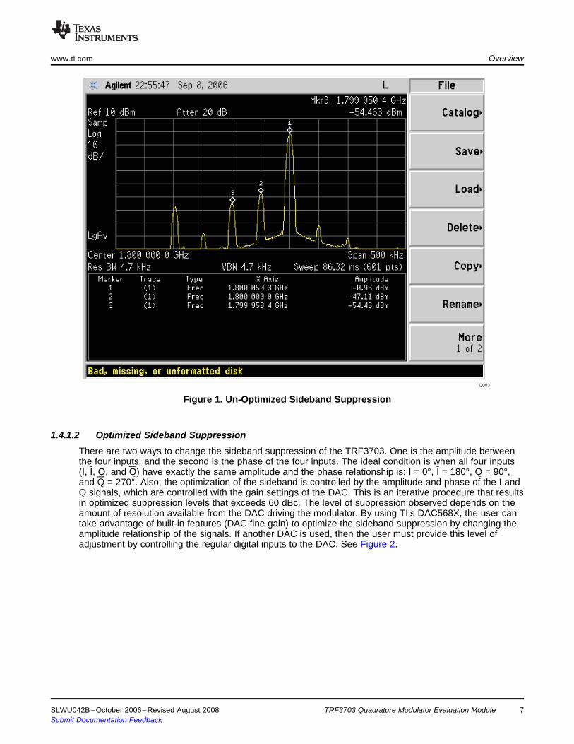
There are two ways to change the sideband suppression of the TRF3703. One is the amplitude betweenthe four inputs, and the second is the phase of the four inputs. The ideal condition is when all four inputs(I, I, Q, and Q) have exactly the same amplitude and the phase relationship is: I = 0°, I = 180°, Q = 90°,and Q = 270°. Also, the optimization of the sideband is controlled by the amplitude and phase of the I andQ signals, which are controlled with the gain settings of the DAC. This is an iterative procedure that resultsin optimized suppression levels that exceeds 60 dBc. The level of suppression observed depends on theamount of resolution available from the DAC driving the modulator. By using TI’s DAC568X, the user cantake advantage of built-in features (DAC fine gain) to optimize the sideband suppression by changing theamplitude relationship of the signals. If another DAC is used, then the user must provide this level ofadjustment by controlling the regular digital inputs to the DAC. See Figure 2.
SLWU042B–October 2006–Revised August 2008 TRF3703 Quadrature Modulator Evaluation Module 7Submit Documentation Feedback
C002
1.4.1.3 Carrier Feedthrough
1.4.1.4 GSM (EDGE EVM Measurements)
Overview www.ti.com
Figure 2. Optimized Sideband Suppression
Carrier feedthrough is the amount of the LO that leaks onto the output spectrum of the modulator. Ideallyfor the TRF3703, inputs (I, I, Q, and Q) must be at approximately 3.3 V for TRF3703-33 and 1.5 V forTRF3703-15. The DAC dc settings are also useful to correct the dc mismatch between I and I andbetween Q and Q to correct for the LO feedthrough. If using TI's DAC568X, then the internal controls forthe IQ offsets provide excellent carrier suppression (very low LO leakage). Alternatively, if an ESG isbeing used, adjust the I and Q voltage offsets in mV steps until you obtain the minimum carrierfeedthrough. A typical carrier feedthrough value exceeds 50 dBm. See Figure 2.
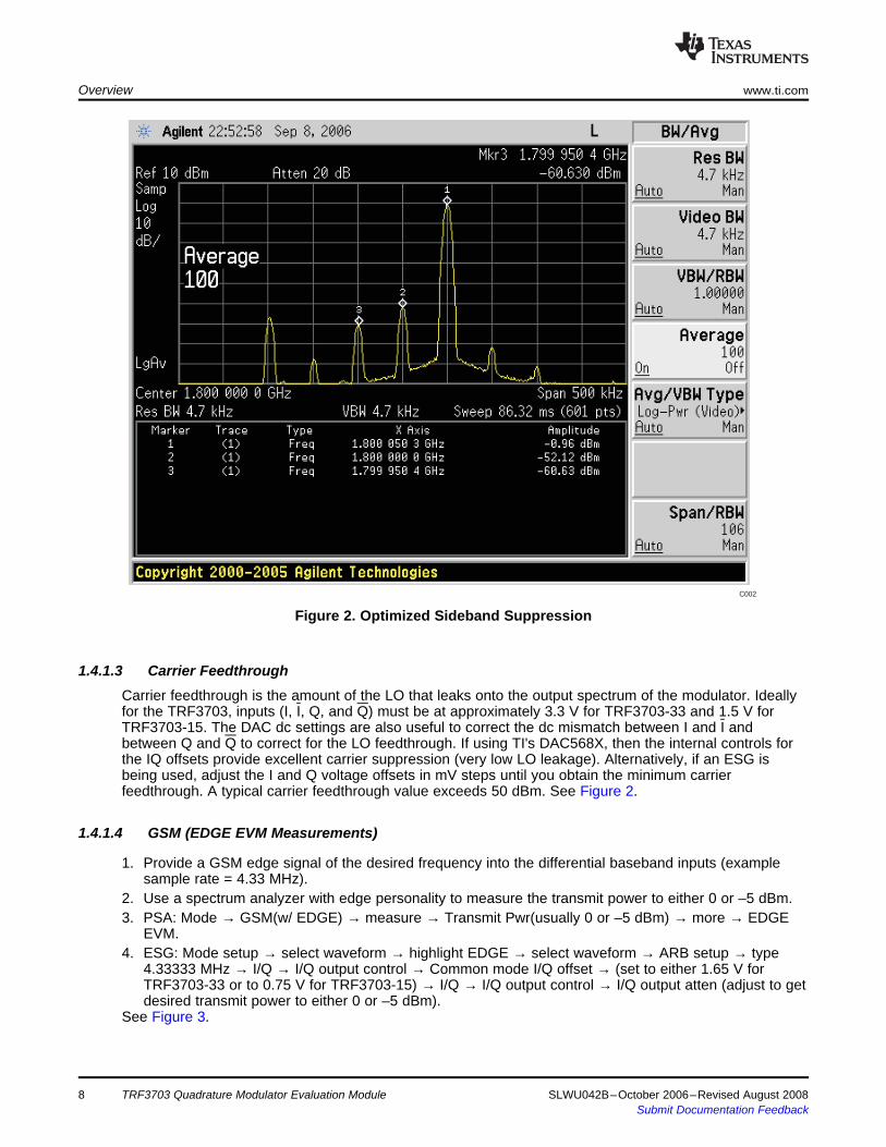
1. Provide a GSM edge signal of the desired frequency into the differential baseband inputs (examplesample rate = 4.33 MHz).
2. Use a spectrum analyzer with edge personality to measure the transmit power to either 0 or –5 dBm.3. PSA: Mode → GSM(w/ EDGE) → measure → Transmit Pwr(usually 0 or –5 dBm) → more → EDGE
EVM.4. ESG: Mode setup → select waveform → highlight EDGE → select waveform → ARB setup → type
4.33333 MHz → I/Q → I/Q output control → Common mode I/Q offset → (set to either 1.65 V forTRF3703-33 or to 0.75 V for TRF3703-15) → I/Q → I/Q output control → I/Q output atten (adjust to getdesired transmit power to either 0 or –5 dBm).
See Figure 3.
8 TRF3703 Quadrature Modulator Evaluation Module SLWU042B–October 2006–Revised August 2008Submit Documentation Feedback
C001
1.4.2 Interface to TI's DAC
www.ti.com Overview
Figure 3. GSM EDGE EVM at 1800 MHz
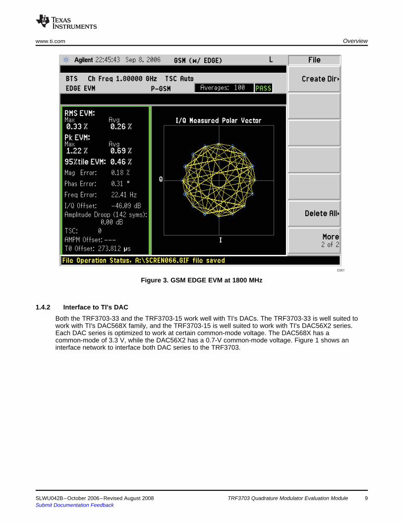
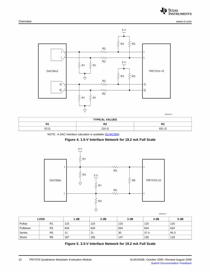
Both the TRF3703-33 and the TRF3703-15 work well with TI's DACs. The TRF3703-33 is well suited towork with TI's DAC568X family, and the TRF3703-15 is well suited to work with TI's DAC56X2 series.Each DAC series is optimized to work at certain common-mode voltage. The DAC568X has acommon-mode of 3.3 V, while the DAC56X2 has a 0.7-V common-mode voltage. Figure 1 shows aninterface network to interface both DAC series to the TRF3703.
SLWU042B–October 2006–Revised August 2008 TRF3703 Quadrature Modulator Evaluation Module 9Submit Documentation Feedback
DAC56x2 TRF3703-15
I I
Q
S0225-01
Q
I I
Q Q
R2
R2
R2
R2
5 V
5 V
R1
R1
R3
R3
R1
R1
R3
R3
DAC568x TRF3703-33
I I
S0226-01
I I
R5
R5
5 V
5 V
R6
R1
R1
R3
R3
Overview www.ti.com
TYPICAL VALUESR1 R2 R3
53 Ω 210 Ω 931 Ω
NOTE: A DAC interface calculator is available (SLWC083).
Figure 4. 1.5-V Interface Network for 19.2 mA Full Scale
LOSS 1 dB 2 dB 3 dB 4 dB 5 dBPullup R1 115 115 115 115 115Pulldown R3 634 634 634 634 634Series R5 11 21 30 37.4 45.3Shunt R6 187 165 147 130 118
Figure 5. 3.3-V Interface Network for 19.2 mA Full Scale
TRF3703 Quadrature Modulator Evaluation Module10 SLWU042B–October 2006–Revised August 2008Submit Documentation Feedback
2 Physical Description
2.1 PCB Layout
K001
www.ti.com Physical Description
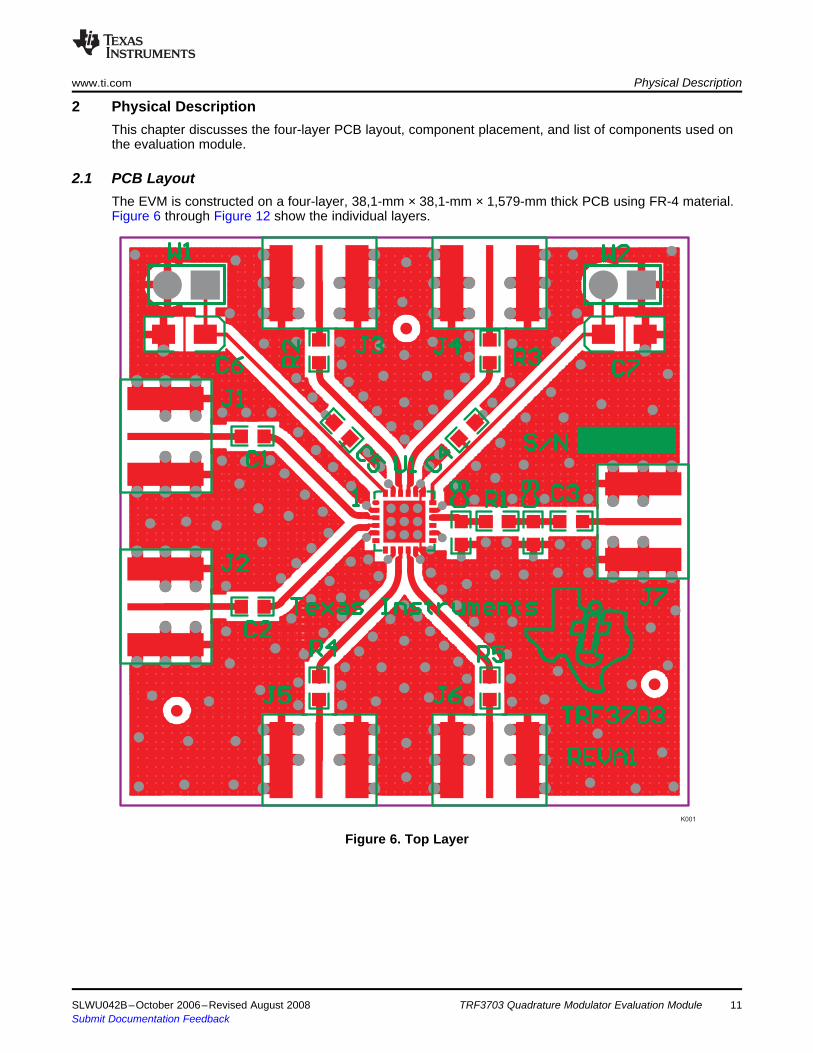
This chapter discusses the four-layer PCB layout, component placement, and list of components used onthe evaluation module.
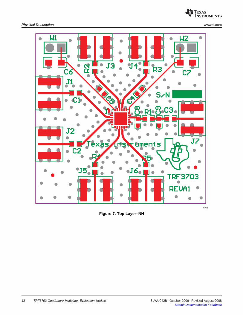
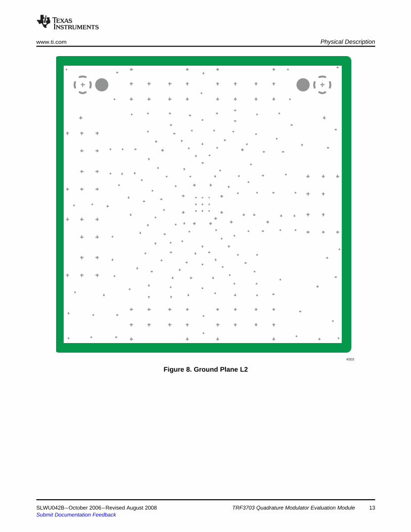
The EVM is constructed on a four-layer, 38,1-mm × 38,1-mm × 1,579-mm thick PCB using FR-4 material.Figure 6 through Figure 12 show the individual layers.
Figure 6. Top Layer
SLWU042B–October 2006–Revised August 2008 TRF3703 Quadrature Modulator Evaluation Module 11Submit Documentation Feedback
K002
Physical Description www.ti.com
Figure 7. Top Layer–NH
12 TRF3703 Quadrature Modulator Evaluation Module SLWU042B–October 2006–Revised August 2008Submit Documentation Feedback
K003
www.ti.com Physical Description
Figure 8. Ground Plane L2
SLWU042B–October 2006–Revised August 2008 TRF3703 Quadrature Modulator Evaluation Module 13Submit Documentation Feedback
K004
Physical Description www.ti.com
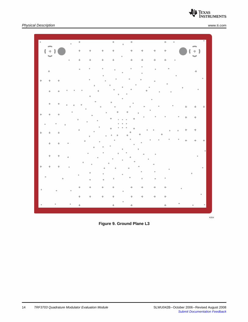
Figure 9. Ground Plane L3
14 TRF3703 Quadrature Modulator Evaluation Module SLWU042B–October 2006–Revised August 2008Submit Documentation Feedback
K005
www.ti.com Physical Description
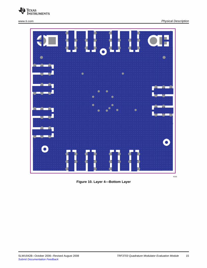
Figure 10. Layer 4—Bottom Layer
SLWU042B–October 2006–Revised August 2008 TRF3703 Quadrature Modulator Evaluation Module 15Submit Documentation Feedback
K006
Physical Description www.ti.com
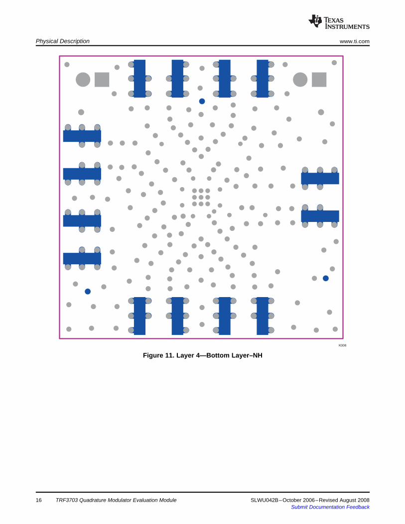
Figure 11. Layer 4—Bottom Layer–NH
16 TRF3703 Quadrature Modulator Evaluation Module SLWU042B–October 2006–Revised August 2008Submit Documentation Feedback
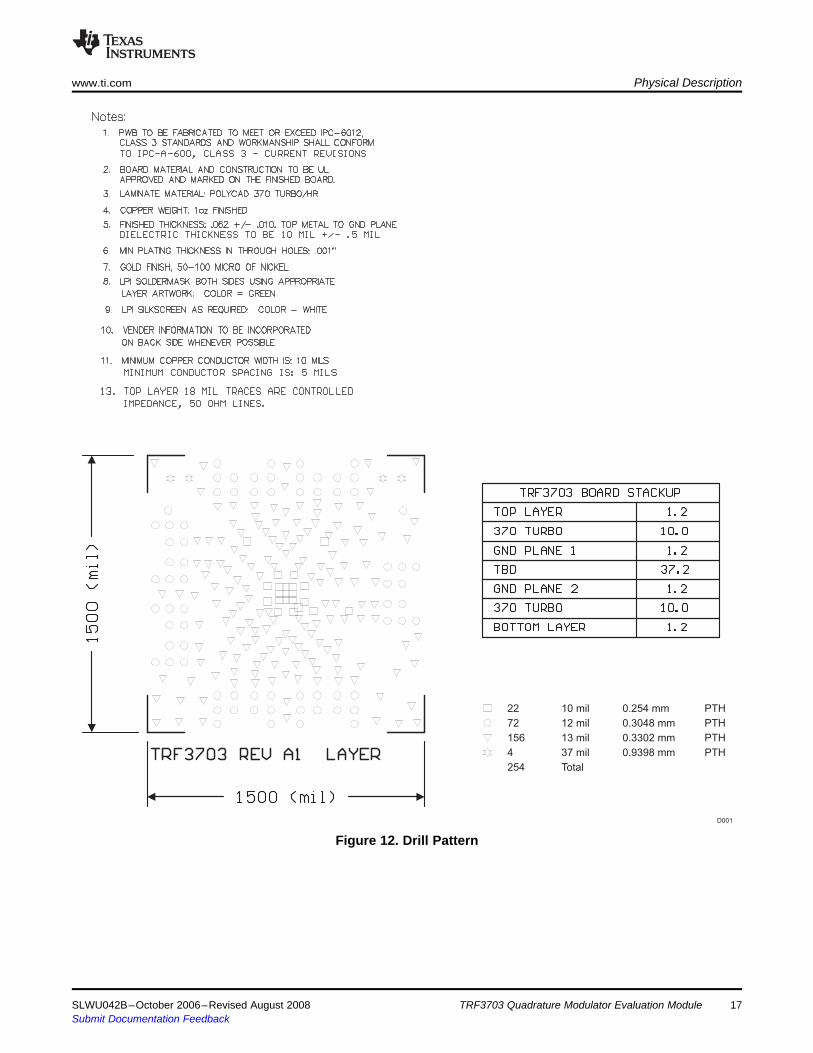
22
72
156
4
254
10 mil
12 mil
13 mil
37 mil
Total
0.254 mm
0.3048 mm
0.3302 mm
0.9398 mm
PTH
PTH
PTH
PTH
D001
www.ti.com Physical Description
Figure 12. Drill Pattern
SLWU042B–October 2006–Revised August 2008 TRF3703 Quadrature Modulator Evaluation Module 17Submit Documentation Feedback
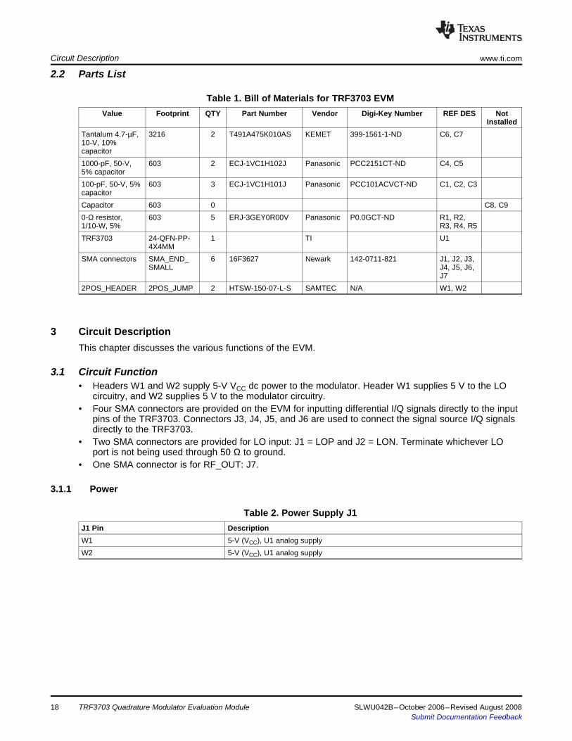
2.2 Parts List
3 Circuit Description
3.1 Circuit Function
3.1.1 Power
Circuit Description www.ti.com
Table 1. Bill of Materials for TRF3703 EVMValue Footprint QTY Part Number Vendor Digi-Key Number REF DES Not
InstalledTantalum 4.7-µF, 3216 2 T491A475K010AS KEMET 399-1561-1-ND C6, C710-V, 10%capacitor1000-pF, 50-V, 603 2 ECJ-1VC1H102J Panasonic PCC2151CT-ND C4, C55% capacitor100-pF, 50-V, 5% 603 3 ECJ-1VC1H101J Panasonic PCC101ACVCT-ND C1, C2, C3capacitorCapacitor 603 0 C8, C90-Ω resistor, 603 5 ERJ-3GEY0R00V Panasonic P0.0GCT-ND R1, R2,1/10-W, 5% R3, R4, R5TRF3703 24-QFN-PP- 1 TI U1
4X4MMSMA connectors SMA_END_ 6 16F3627 Newark 142-0711-821 J1, J2, J3,
SMALL J4, J5, J6,J7
2POS_HEADER 2POS_JUMP 2 HTSW-150-07-L-S SAMTEC N/A W1, W2
This chapter discusses the various functions of the EVM.
• Headers W1 and W2 supply 5-V VCC dc power to the modulator. Header W1 supplies 5 V to the LOcircuitry, and W2 supplies 5 V to the modulator circuitry.
• Four SMA connectors are provided on the EVM for inputting differential I/Q signals directly to the inputpins of the TRF3703. Connectors J3, J4, J5, and J6 are used to connect the signal source I/Q signalsdirectly to the TRF3703.
• Two SMA connectors are provided for LO input: J1 = LOP and J2 = LON. Terminate whichever LOport is not being used through 50 Ω to ground.
• One SMA connector is for RF_OUT: J7.
Table 2. Power Supply J1J1 Pin DescriptionW1 5-V (VCC), U1 analog supplyW2 5-V (VCC), U1 analog supply
18 TRF3703 Quadrature Modulator Evaluation Module SLWU042B–October 2006–Revised August 2008Submit Documentation Feedback
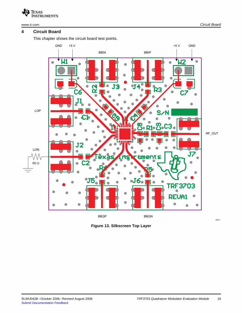
4 Circuit Board
BBQP BBQN
+5 V
BBIPBBIN
LOP
LON
+5 VGND GND
50 W
RF_OUT
K001
www.ti.com Circuit Board
This chapter shows the circuit board test points.
Figure 13. Silkscreen Top Layer
SLWU042B–October 2006–Revised August 2008 TRF3703 Quadrature Modulator Evaluation Module 19Submit Documentation Feedback
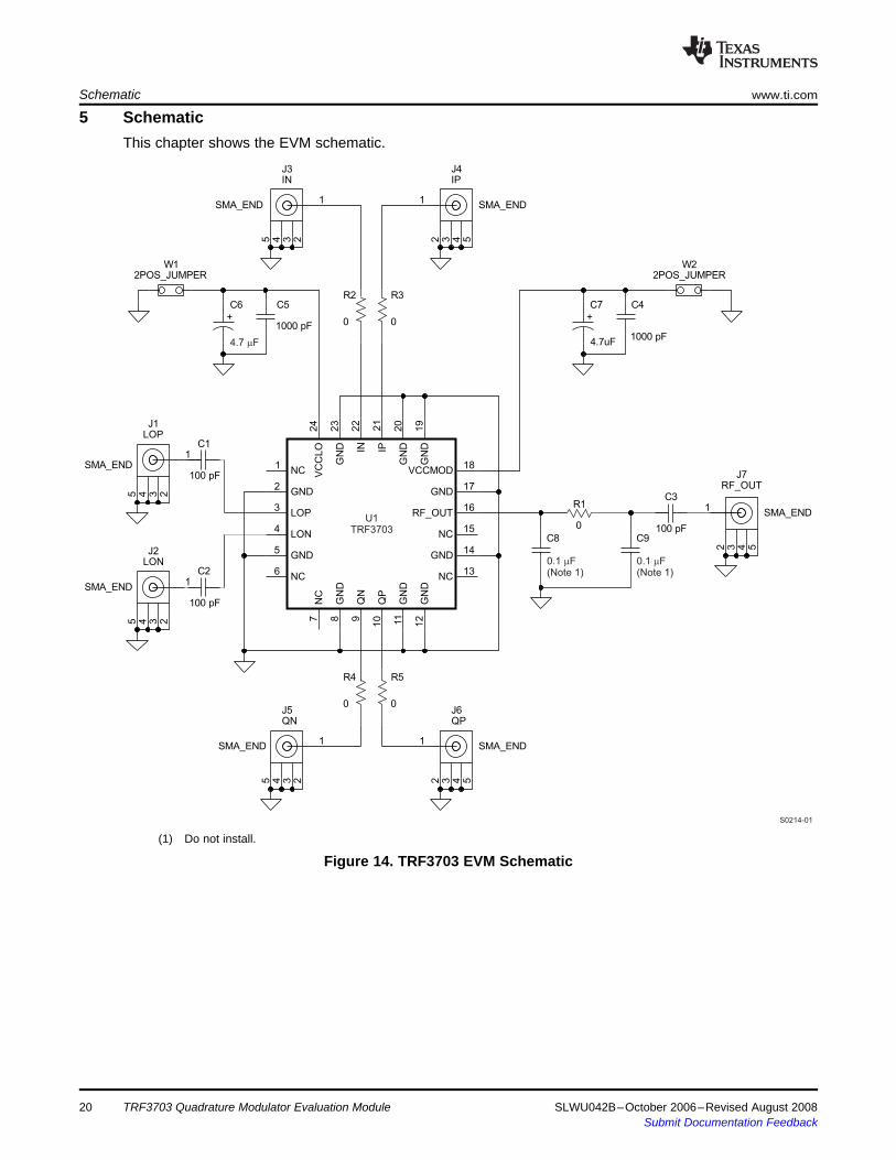
5 Schematic
C1
100 pF
C2
100 pF
1
J1
SMA_ENDNC
1
GND2
LOP3
LON4
GND5
NC6
NC
7
GN
D8
QN
9
QP
10
GN
D11
GN
D1
2
NC13
GND14
NC15
RF_OUT16
GND17
VCCMOD18G
ND
19
GN
D2
0
I P2
1
IN2
2
GN
D2
3
VC
CLO
24
LOP
1
22
33
44
55
J2
SMA_END
LON
1
2345
J3
SMA_END
IN
1
2 3 4 5
J4
SMA_END
IP
C5
1000 pF
1
2 3 4 5
J7
SMA_END
C3
100 pF
C4
1000 pF
1
2345
J5
SMA_END
QN
1
2 3 4 5
J6
SMA_END
QP
RF_OUT
W12POS_JUMPER
W22POS_JUMPER
C8 C9
R1
0
+
C6
+
C7
4.7uF
R4
0
R5
0
R2
0
R3
0
S0214-01
0.1 F(Note 1)
m 0.1 F(Note 1)
m
4.7 Fm
U1TRF3703
Schematic www.ti.com
This chapter shows the EVM schematic.
(1) Do not install.
Figure 14. TRF3703 EVM Schematic
20 TRF3703 Quadrature Modulator Evaluation Module SLWU042B–October 2006–Revised August 2008Submit Documentation Feedback
EVALUATION BOARD/KIT IMPORTANT NOTICETexas Instruments (TI) provides the enclosed product(s) under the following conditions:This evaluation board/kit is intended for use for ENGINEERING DEVELOPMENT, DEMONSTRATION, OR EVALUATION PURPOSESONLY and is not considered by TI to be a finished end-product fit for general consumer use. Persons handling the product(s) must haveelectronics training and observe good engineering practice standards. As such, the goods being provided are not intended to be completein terms of required design-, marketing-, and/or manufacturing-related protective considerations, including product safety and environmentalmeasures typically found in end products that incorporate such semiconductor components or circuit boards. This evaluation board/kit doesnot fall within the scope of the European Union directives regarding electromagnetic compatibility, restricted substances (RoHS), recycling(WEEE), FCC, CE or UL, and therefore may not meet the technical requirements of these directives or other related directives.Should this evaluation board/kit not meet the specifications indicated in the User’s Guide, the board/kit may be returned within 30 days fromthe date of delivery for a full refund. THE FOREGOING WARRANTY IS THE EXCLUSIVE WARRANTY MADE BY SELLER TO BUYERAND IS IN LIEU OF ALL OTHER WARRANTIES, EXPRESSED, IMPLIED, OR STATUTORY, INCLUDING ANY WARRANTY OFMERCHANTABILITY OR FITNESS FOR ANY PARTICULAR PURPOSE.The user assumes all responsibility and liability for proper and safe handling of the goods. Further, the user indemnifies TI from all claimsarising from the handling or use of the goods. Due to the open construction of the product, it is the user’s responsibility to take any and allappropriate precautions with regard to electrostatic discharge.EXCEPT TO THE EXTENT OF THE INDEMNITY SET FORTH ABOVE, NEITHER PARTY SHALL BE LIABLE TO THE OTHER FOR ANYINDIRECT, SPECIAL, INCIDENTAL, OR CONSEQUENTIAL DAMAGES.TI currently deals with a variety of customers for products, and therefore our arrangement with the user is not exclusive.TI assumes no liability for applications assistance, customer product design, software performance, or infringement of patents orservices described herein.Please read the User’s Guide and, specifically, the Warnings and Restrictions notice in the User’s Guide prior to handling the product. Thisnotice contains important safety information about temperatures and voltages. For additional information on TI’s environmental and/orsafety programs, please contact the TI application engineer or visit www.ti.com/esh.No license is granted under any patent right or other intellectual property right of TI covering or relating to any machine, process, orcombination in which such TI products or services might be or are used.
FCC WarningThis evaluation board/kit is intended for use for ENGINEERING DEVELOPMENT, DEMONSTRATION, OR EVALUATION PURPOSESONLY and is not considered by TI to be a finished end-product fit for general consumer use. It generates, uses, and can radiate radiofrequency energy and has not been tested for compliance with the limits of computing devices pursuant to part 15 of FCC rules, which aredesigned to provide reasonable protection against radio frequency interference. Operation of this equipment in other environments maycause interference with radio communications, in which case the user at his own expense will be required to take whatever measures maybe required to correct this interference.
Mailing Address: Texas Instruments, Post Office Box 655303, Dallas, Texas 75265Copyright © 2008, Texas Instruments Incorporated
EVM WARNINGS AND RESTRICTIONSIt is important to operate this EVM within the input voltage range of 4.5 V to 5.5 V and the output voltage range of 4.5 V to 5.5 V.Exceeding the specified input range may cause unexpected operation and/or irreversible damage to the EVM. If there are questionsconcerning the input range, please contact a TI field representative prior to connecting the input power.Applying loads outside of the specified output range may result in unintended operation and/or possible permanent damage to the EVM.Please consult the EVM User's Guide prior to connecting any load to the EVM output. If there is uncertainty as to the load specification,please contact a TI field representative.During normal operation, some circuit components may have case temperatures greater than 59°C. The EVM is designed to operateproperly with certain components above –40°C as long as the input and output ranges are maintained. These components include but arenot limited to linear regulators, switching transistors, pass transistors, and current sense resistors. These types of devices can be identifiedusing the EVM schematic located in the EVM User's Guide. When placing measurement probes near these devices during operation,please be aware that these devices may be very warm to the touch.
Mailing Address: Texas Instruments, Post Office Box 655303, Dallas, Texas 75265Copyright © 2008, Texas Instruments Incorporated

IMPORTANT NOTICETexas Instruments Incorporated and its subsidiaries (TI) reserve the right to make corrections, modifications, enhancements, improvements,and other changes to its products and services at any time and to discontinue any product or service without notice. Customers shouldobtain the latest relevant information before placing orders and should verify that such information is current and complete. All products aresold subject to TI’s terms and conditions of sale supplied at the time of order acknowledgment.TI warrants performance of its hardware products to the specifications applicable at the time of sale in accordance with TI’s standardwarranty. Testing and other quality control techniques are used to the extent TI deems necessary to support this warranty. Except wheremandated by government requirements, testing of all parameters of each product is not necessarily performed.TI assumes no liability for applications assistance or customer product design. Customers are responsible for their products andapplications using TI components. To minimize the risks associated with customer products and applications, customers should provideadequate design and operating safeguards.TI does not warrant or represent that any license, either express or implied, is granted under any TI patent right, copyright, mask work right,or other TI intellectual property right relating to any combination, machine, or process in which TI products or services are used. Informationpublished by TI regarding third-party products or services does not constitute a license from TI to use such products or services or awarranty or endorsement thereof. Use of such information may require a license from a third party under the patents or other intellectualproperty of the third party, or a license from TI under the patents or other intellectual property of TI.Reproduction of TI information in TI data books or data sheets is permissible only if reproduction is without alteration and is accompaniedby all associated warranties, conditions, limitations, and notices. Reproduction of this information with alteration is an unfair and deceptivebusiness practice. TI is not responsible or liable for such altered documentation. Information of third parties may be subject to additionalrestrictions.Resale of TI products or services with statements different from or beyond the parameters stated by TI for that product or service voids allexpress and any implied warranties for the associated TI product or service and is an unfair and deceptive business practice. TI is notresponsible or liable for any such statements.TI products are not authorized for use in safety-critical applications (such as life support) where a failure of the TI product would reasonablybe expected to cause severe personal injury or death, unless officers of the parties have executed an agreement specifically governingsuch use. Buyers represent that they have all necessary expertise in the safety and regulatory ramifications of their applications, andacknowledge and agree that they are solely responsible for all legal, regulatory and safety-related requirements concerning their productsand any use of TI products in such safety-critical applications, notwithstanding any applications-related information or support that may beprovided by TI. Further, Buyers must fully indemnify TI and its representatives against any damages arising out of the use of TI products insuch safety-critical applications.TI products are neither designed nor intended for use in military/aerospace applications or environments unless the TI products arespecifically designated by TI as military-grade or "enhanced plastic." Only products designated by TI as military-grade meet militaryspecifications. Buyers acknowledge and agree that any such use of TI products which TI has not designated as military-grade is solely atthe Buyer's risk, and that they are solely responsible for compliance with all legal and regulatory requirements in connection with such use.TI products are neither designed nor intended for use in automotive applications or environments unless the specific TI products aredesignated by TI as compliant with ISO/TS 16949 requirements. Buyers acknowledge and agree that, if they use any non-designatedproducts in automotive applications, TI will not be responsible for any failure to meet such requirements.Following are URLs where you can obtain information on other Texas Instruments products and application solutions:Products ApplicationsAmplifiers amplifier.ti.com Audio www.ti.com/audioData Converters dataconverter.ti.com Automotive www.ti.com/automotiveDSP dsp.ti.com Broadband www.ti.com/broadbandClocks and Timers www.ti.com/clocks Digital Control www.ti.com/digitalcontrolInterface interface.ti.com Medical www.ti.com/medicalLogic logic.ti.com Military www.ti.com/militaryPower Mgmt power.ti.com Optical Networking www.ti.com/opticalnetworkMicrocontrollers microcontroller.ti.com Security www.ti.com/securityRFID www.ti-rfid.com Telephony www.ti.com/telephonyRF/IF and ZigBee® Solutions www.ti.com/lprf Video & Imaging www.ti.com/video
Wireless www.ti.com/wireless
Mailing Address: Texas Instruments, Post Office Box 655303, Dallas, Texas 75265Copyright © 2008, Texas Instruments Incorporated