tribhuvan university institute of engineering pulchowk...
TRANSCRIPT

TRIBHUVAN UNIVERSITY INSTITUTE OF ENGINEERING
PULCHOWK CAMPUS
DEPARTMENT OF ELECTRONICS AND COMPUTER ENGINEERING
A
FINAL YEAR REPORT
ON
SoC Approach in Designing Vision Based Robot
By:
Bishesh Khanal (Exam Roll No 16113)
Deepak Parajuli (Exam Roll No 16115)
Dinesh Twanabasu (Exam Roll No 16116)
Suman Raj Bista (Exam Roll No 16138)
Kathmandu, Nepal
March, 2009

TRIBHUVAN UNIVERSITY INSTITUTE OF ENGINEERING
PULCHOWK CAMPUS
DEPARTMENT OF ELECTRONICS AND COMPUTER ENGINEERING
A
FINAL YEAR REPORT
ON
SoC Approach in Designing Vision Based Robot
By:
Bishesh Khanal (Exam Roll No16113)
Deepak Parajuli (Exam Roll No 16115)
Dinesh Twanabasu (Exam Roll No 16116)
Suman Raj Bista (Exam Roll No 16138)
A PROJECT WAS SUBMITTED TO THE DEPARTMENT OF ELECTRONICS AND
COMPUTER ENGINEERING IN PARTIAL FULLFILLMENT OF THE
REQUIREMENT FOR THE BACHELOR OF ENGINEERING
Kathmandu, Nepal
March, 2009

I
ACKNOWLEDGEMENT
While working with our project, we have received immense help and support from staff at
department of electronics and computer engineering, students at Robotics club and our parents
and friends. From the department we would like to thank our project supervisor Prof. Dr.
Shashidhar Ram Joshi for his guidance and support, as well as Mr. Dipen Chapagain and
Associate Prof. Dr Jyoti Tandulkar. From robotics club we would like to thank our juniors
Bikram Adhikari, Bikrant Gautam, Chandra Prakash Thapa, Deepak Gurung, Giresh Singh
Kunwar, Kapil Pudasaini , Nawaraj Gurung, Prashant Gyawali and Sumit Kumar Bum for their
persistent curiosity and interest in our project, and ever ready helping hands. Working in robotics
club lab would not have been such a fun without them.
We would also like to thank our seniors Ramesh Chaudhary and Suraj Karki for their advice and
support while working in the robotics club for more than two years. Finally, many thanks to our
parents who have always supported and encouraged us and never complained about so many
sleepless nights during the project.

II
ABSTRACT
Vision system is an important part of autonomous robots. Adding a vision system onboard to a
robot requires a control system with a lot of processing power at high speed. Traditional systems
with microprocessors or DSPs find it extremely difficult to meet real time requirements of high
speed vision systems for small robots. This project demonstrates the use of SoC approach in
designing vision based robots. The video data is passed directly from CMOS image sensor to the
FPGA where preprocessing of the data is done. Color recognition and edge detection is
implemented in hardware. This relieves CPUs or DSPs from tedious repetitive tasks and allows
them to focus on more complicated tasks. Software written to MicroBlaze, a 32-bit soft-core
RISC processor, within the same FPGA then performs object recognition and provides
commands to stepper controller. Stepper controller, a hardware module implemented within the
FPGA, generates required signals to drive different motors present in Microbot TeachMover for
a desired motion.
The system at present recognizes objects of red, white and black. The complete system stands as
a starting base platform for more complex vision tasks and planning of control actions for
autonomous robots.

III
TABLE OF CONTENTS
ACKNOWLEDGEMENT I
ABSTRACT II
LIST OF FIGURES VI
LIST OF ABBREVIATIONS VII
1 INTRODUCTION 1
1.1 Motivation....................................................…..........................................................................1
1.2 Background....................................................................................................................1
1.3 Objectives.................................................................................................................….2
1.4 Design Methodology..................................................................................................…2
1.5 Design Decisions...........................................................................................................3
1.5.1 Xilinx’s FPGA..........................................................................…............…..3
1.5.2 C3038 image sensor module...........................................................................3
1.5.3 Color Space..........................................................................................................…...4
1.5.4 Microbot TeachMover....................................................................................4
2 LANGUAGE TOOLS 5
2.1Integrated Software Environment...................................................................................5
2.2Embedded Development Kit....................................…...................................................5
2.2.1Xilinx Platform Studio.....................................................................................5
2.2.2 Software Development Kit......................................................................…...5
2.2.3 Other EDK Components..........................................................................…...6
2.3 ChipScope Pro..................................................................................................….........6
3 THEORITICAL BACKGROUND 8
3.1 FPGA and SoC..........................................................................................................….8
3.2 MicroBlaze.....................................................................................................................9
3.3 Color Spaces.........................................................................................................…...10
3.4 Edge Detection.............................................................................................................11

IV
3.5 Object Recognition .................................................................................................…11
3.5.1 Hough Transform..........................................................................................12
3.6 VGA Display.........................................................................................................…..12
3.6.1 Signal timing for 640*480 VGA display...............................................…...13
3.6.2 Synchronization signal timing......................................................................14
3.7 Stepper Motor........................................................................................................…..15
3.8 MOSFET......................................................................................................................16
3.9 I2C Interface..........................................................................................................…...16
4. DESIGN AND IMPLEMENTATION 18
4.1 System Block Diagram................................................................................................18
4.2 Hardware Implementation.................................................................................…......19
4.2.1 I2C Interface........…................................................................................…19
4.2.2 Framegrabber...................................................................................….......20
4.2.3 UV_Separator.....................................................................................................…22
4.2.4 Color_Recognition............,..............................................................….....…23
4.2.5 Edge Detector................................................................................................25
I) Moving Window....................................................................................25
II) Sobel Edge Calculation.......................................…........................…..27
4.2.6 Video Display System.......................................................................…........29
I) Memory Controller.................................................................................30
II) VGA Controller...............................................................................….32
4.2.7 Motor Control Module...................................................................…......….33
4.2.8 Motor Driver Circuit and PCB fabrication...................................................36
I) Driver circuit..........................................................................................36
II) PCB fabrication ....................................................................................37
4.3 Software Specification.................................................................................................38
4.3.1 Edge Detection....................................…......................................................38
4.3.2 Object Detection...........................................................................................40
4.3.3 Color Detection.........................................................................................…42

V
5. RESULTS 43
6 CONCLUSIONS AND RECOMMENDATION 44
6.1 Conclusion ........................................…................................................................…..44
6.2Recommendation..........................................................................................................44
REFERENCES 45
APPENDIX A 49
APPENDIX B 51

VI
LIST OF FIGURES
Figure 1 Microbot............................................................................................................................4
Figure 2 Basic Embedded Design Process Flow.............................................................................6
Figure 3 MicroBlaze Core Block Diagram....................................................................................10
Figure 1 YCrCb BARS....…..........................................................................................................11
Figure 2 The Hough Transform................................................….................................................12
Figure 3 VGA output.....................................................................................................................13
Figure 4 VGA Display Timing......................................................................................................14
Figure 5 VGA Control Timing................................................…..................................................15
Figure 6 Schematic diagram of N-channel Power MOSFET........................................................16
Figure 7 Transmitting address sub-address and data...................................................................17
Figure 8 System Block Diagram..................................................................................................18
Figure 12 Block Diagram of the I2C module.................................................................................19
Figure 13 Simulation of I2C module............................................…..............................................20
Figure 14 Block Diagram of the framegrabber module ................................................................20
Figure 15 Simulation of framegrabber module....................................…......................................21
Figure 16 Real-time signal capture of framegrabber module........................................................22
Figure 17 Block Diagram of theUV_separotor........................................................................…..22
Figure 18 Simulation of the UV_separator module................................................................…...23
Figure 19 Real-time signal capture of the UV_separator module.................................................23
Figure 20 Block Diagram of the Color_recognition..................................................................... 24
Figure 21 Simulation of the Color_recognition module................................................................24
Figure 22 Real-time signal capture of the Color_recognition module..........................................25
Figure 23 Block Diagram of the Moving_window module...........................................................25
Figure 24 The architecture of the 3x3 moving window.................................................................26
Figure 25 Simulation of the Moving_window module..................................................................27
Figure 26 Block Diagram of the sobel_edge module................................................................…27
Figure 27 Hardware implementation of Sobel Edge Detection................................................….28
Figure 28 Simulation of the Sobel_edge module...........................................................................29

VII
Figure 29 Block Diagram of the Video Display system................................................................30
Figure 30 Block Diagram of the Memory controller module........................................................30
Figure 31 Simple dual port RAM core schematic symbol.........................................................…32
Figure 32 Simulation of the Memory Controller module..............................................................32
Figure 33 Block Diagram of the VGA_controller module........................................................…32
Figure 34 Simulation of the VGA_controller module...................................................................33
Figure 35 Block Diagram of the Motor Driver module.................................................................34
Figure 36 Block diagram of stepper motor controlling.................................................................35
Figure 37 Simulation of the stepper Motor Controller .................................................................35
Figure 38 Driver circuit for driving stepper motor coil.................................................................36
Figure 39 PCB layout of the stepper driver circuit........................................................................37
Figure 40 Horizontal and vertical operators..................................................................................38
Figure 41 Image and Convolution Mask................................................................................…...38
Figure 42 Simulation of Edge detection in Visual C++.................................................................39
Figure 43 Simulation of Object Detection in Matlab................................................................….41
Figure 44 YUV range................................................................................................................….42
Figure 45 Simulation of Color detection in Visual C++................................................................42
Table 1 640X480 resolutionVGATiming..................................................................................…14
Table 2 Comparison between hardware and software to determine whether the given pixel is
edge or not ........................................................................................................................43

VIII
LIST OF ABBREVATIONS
ABU - Asian Broadcasting Union
ACK - Acknowledge
ADC - Analog to Digital Converter
ASM - Algorithmic State Machine
BRAM - Block Random Access Memory
CCD - Charge Coupled Device
CMOS - Complementary Metal Oxide Semiconductor
CPLD - Complex Programmable Logic Device
CPU - Central Processing Unit
CRT - Cathode Ray Tube
DAC - Digital to Analog Converter
DC - Direct Current
DSP - Digital Signal Processor
EDK - Embedded Development Kit
EEPROM - Electrically Erasable Programmable ROM
FIFO - First In First Out
FPGA - Field Programmable Gate Array
FSL - Fast Simplex Link
FSM - Finite State Machine
HS - Horizontal Synchronization
IIC - Inter Integrated Circuit
IP - Intellectual Property
IOE – Institute Of Engineering
ISE - Integrated Software Environment
LMB- Local Memory Bus
MOSFET- Metal Oxide Semiconductor Field Effect Transistor
MSB- Most Significant Bit
NTSC - National Television System Committee
PAL - Phase Alternation Line

IX
PCB - Printed Circuit Board
PCLK- Pixel clock
PLB - Processor Local Bus
RAM - Random Access Memory
RGB -Red Green Blue
ROM - Read Only Memory
SCL - Serial Clock
SDA - Serial Data
SDK - Software Development Kit
SECAM - Sequentiel Couleur Avec Mémoire or Sequential Color with Memory
SoC - System On Chip
SoPC - System on Programmable Chip
SPI – Serial Peripheral Interface
TTL - Transistor Transistor Logic
TV-Television
UART- Universal Asynchronous Receiver Transmitter
VCC- Voltage Connected to Collector
VGA- Video Graphic Array
VHDL- VHSIC Hardware Description Language
VHSIC-Very High Speed Integrated Circuits
VS -Vertical Synchronization
VSYNC-vertical synchronization
XPS -Xilinx Platform Studio
XST- Xilinx Synthesis Tool

1
1. INTRODUCTION
This report explains the objective and implementation of SoC approach in designing vision based
robotic system.
1.1 Motivation
Vision system can be a very important part of a robot in many applications. High speed image
processing is a crucial element in applications like autonomous robot navigation [1]. A robot can
get information about the surroundings, objects, and the path it is travelling with the help of a
vision system. However, adding a vision system to a robot demands a lot of computing power
and speed. Processing a large amount of image data in real time is a challenge that has interested
researchers all around the world.
A number of robots have been built in Robotics Club, Pulchowk engineering campus in the last
eight years. Most of these robots were primarily built for the ABU ROBOCON, an international
robotic competition for undergraduate students of Asia Pacific region. None of them had vision
capabilities.
A robot capable of tracking a specific colored ball was developed in 2005 that used a laptop for
the vision processing task [2]. This system was too bulky to be placed in small robots and too
slow for high speed navigation. Thus a new approach in designing vision based robots is
required.
1.2 Background
Algorithms designed in software to work in a processor are not parallel in nature. Therefore,
using a single CPU for image acquisition and processing makes it extremely difficult to match
real time requirements [3, 4]. The limitations present in implementing real time image processing
algorithms in traditional CPU and DSPs have made researchers seek other options. The inherent
parallelism present in hardware designed within FPGA makes it one of the suitable alternatives
for image processing tasks. FPGA based vision systems can achieve speeds in orders of

2
magnitude faster than the traditional systems [5, 6]. This has increased the interest in developing
FPGA based vision system.
1.3 Objectives
The main objective of the project is to demonstrate the advantages of SoC approach in designing
vision based robot. The project creates a set of hardware and software modules integrated in a
single FPGA chip which can be used as a base system for implementing complex vision
algorithms and test it in real time robotic system.
The robot in which the system is implemented should detect an object with a specific color or
shape in a controlled environment, using data from image sensor in real time.
1.4 Design methodology
We broke down the system into a number of modules. Each module was tested and verified in
different levels before integrating with the higher level system components. An integration of
one module with another was immediately followed by testing of the combined modules before
integrating with the remaining system. This sort of incremental testing approach was very
important because testing and debugging of all the integrated hardware and software at once
would be extremely difficult.
When a hardware module was completed, we simulated its behavioral model using ModelSim.
Then we carried out post map simulation using ISE and ModelSim that uses netlists generated by
the synthesis tool XST. This model is most likely to imitate the actual working in FPGA than the
behavioral model used in simulation with ModelSim. For both of these simulations we developed
VHDL test benches of the corresponding hardware module being simulated.
We tested and debugged actual hardware designs with ChipScope pro, Logic analyzer and using
leds and push buttons available in the Xilinx development board.
We tested each of the vision algorithms in software either using MATLAB or Visual C++. After
the algorithms were found to be suitable for our experiment, we implemented them either in
FPGA hardware or in MicroBlaze processor,

3
The contributions of each of us to this project:
i) Bishesh Khanal : Overall concept of the project; device selection; learning using EDK, ISE
and ChipScope pro; framegrabber module and implementation of the selected image processing
algorithms in hardware (color recognition and edge detection).
ii) Deepak Parajuli: Implementation of video display system in FPGA hardware; External
interface and connection of camera with the FPGA through EXP prototype module.
iii) Dinesh Twanabasu: Stepper controller; Stepper driver circuit and PCB design; selection of
Microbot as the test robotic system; using motors of Microbot for required motion and I2C
interface for configuring camera.
iv) Suman Raj Bista: Selection of image processing algorithms and verification in software;
learning using EDK, XPS design flow; system integration and software development in
MicroBlaze.
1.5 Design Decisions
1.5.1 Xilinx’s FPGA
Xilinx’s FPGAs have been used in IOE in previous years. Getting a complete system of
hardware and software to work in SoC design paradigm requires a lot of experience [7], well
developed and easy to use development tools. Xilinx provides a lot of application notes and
reference designs that are important while learning the tools and software to design a complete
integrated system. Thus we selected Xilinx’s Spartan 3A DSP 1800A development board for the
project.
1.5.2 C3038 Image sensor module
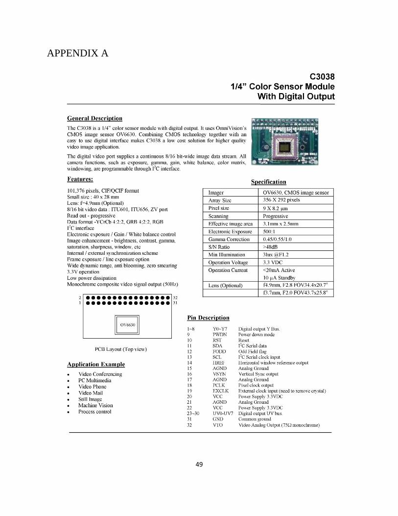
We have used C3038 color module that uses OmniVision’s OV6630 CMOS image sensor.
CMOS image sensors provide data in digital form unlike CCD sensors. OV6630 sensor provides
the image of maximum size of 352X288 at 50 frames per second in progressive scan mode.
Moderate price of this particular sensor was also considered during the selection process.

4
1.5.3 Color space
The C3038 color sensor module used in our project gives data in two formats YUV and RGB. In
RGB color space luminance components are mixed with chrominance and therefore it is not
reliable for color segmentation in varying light intensities [8]. We have selected YCrCb (YUV)
color space to be used for color recognition and edge detection.
1.5.4 Microbot TeachMover
Figure 1 Microbot
Microbot TeachMover is a robotic arm used for the teaching of robotic fundamentals simulating
industrial robot operations. TeachMovers are used in elementary and secondary schools,
colleges, universities and industrial training programs [9]. Microbot uses six 4-bit stepper motors
to provide motion to different parts. The six parts controlled are Base, Shoulder, Hand, Elbow,
Left wrist, and Right wrist. Microbot is available in our department in IOE. Our major interest in
the project lied with the electronic system and we decided to test our system in Microbot because
we need not spend much time and effort in mechanical aspects of the robot.

5
2. LANGUAGE AND TOOLS
We have used VHDL to describe the hardware designed and synthesize them in FPGA. Software
is designed using C language in the SDK that comes with the Xilinx’s EDK.
Embedded systems are somewhat complex. Getting the hardware and software portions of an
embedded design to work in an integrated form can be projects in themselves for people with no
previous design experience with HDLs and digital systems. Merging the two design components
so they function as one integrated system brings additional challenges. Making such designs to
work requires a good knowledge of design software tools. For systems with MicroBlaze, EDK
simplifies the design process. Along with EDK, Xilinx offers several sets of tools which are
briefly described below:
2.1 Integrated Software Environment
ISE is the foundation for Xilinx FPGA logic design. Xilinx has provided software development
tools that allow some simplification to the complex and involved process of designing hardware
to the FPGA. Various utilities such as constraints entry, timing analysis, logic placement and
routing, and device programming have all been integrated into ISE [10].
2.2 Embedded Development Kit
EDK is a suite of tools and Intellectual Property that enables to design a complete embedded
processor system for implementation in a Xilinx FPGA device. It can be thought as an umbrella
covering all things related to embedded processor systems and their design. The Xilinx ISE
software must also be installed to run EDK. It consists of:
2.2.1 Xilinx Platform Studio
The Xilinx Platform Studio (XPS) is the development environment or GUI used for designing
the hardware portion of embedded processor system.
2.2.2 Software Development Kit

6
Platform Studio Software Development Kit (SDK) is an integrated development environment,
complimentary to XPS, that is used for C/C++ embedded software application creation and
verification. SDK is built on the Eclipse open-source framework.
2.2.3 Other EDK Components [10]
• Hardware IP for the Xilinx embedded processors
• Drivers and libraries for embedded software development
• GNU Compiler and debugger for C/C++ software development targeting the MicroBlaze
processors.
2.3 ChipScope Pro
ChipScope is a set of tools from Xilinx that allows monitoring signals and buses of the user
designed hardware system within the FPGA. Monitoring signals of the hardware within FPGA
chip is not possible with the conventional Logic Analyzers. This makes ChipScope an important
tool in debugging hardware designed in FPGA. However, sample memory of the analyzer is
limited by the memory resources available within the FPGA and the memory resources used by
the design being tested. It also cannot detect all the glitches in the system because it uses the
clock signal of the system being tested.
Figure 2 Basic Embedded Design Process Flow (from [10], page number: 14)

7
Besides above mentioned tools we used Matlab and Visual C++ for verifications of image
processing algorithms, ModelSim for the simulation of Hardware designs like frame grabber,
motor controller.

8
3. THEORITICAL BACKGROUND
3.1 FPGA and SoC
FPGA is a semiconductor device that can be configured to realize digital systems ranging from
basic logic functions like NAND, NOR etc to some complex combinational and sequential
functions. It consists of a matrix of reconfigurable gate array logic circuitry. When a FPGA is
configured, the internal circuitry is connected in a way that creates a hardware implementation of
the designs that are usually described using HDLs. Unlike processors, FPGAs use dedicated
hardware for processing logic and do not have an operating system. Hardware designed in
FPGAs can be truly parallel in nature and therefore these hardware that can have different
processing operations do not have to compete for the same resources. Unlike hard-wired PCB
designs which have fixed hardware resources, FPGA-based systems can literally rewire their
internal circuitry to allow reconfiguration after the system is deployed to the field [11, 12].
A complex digital system needs different components like processors, memory, operating
system, electronic functions, timers, interrupt controllers, interfaces like firewire and USB, and
basic software utilities. [13] All the components of a complex digital system could be integrated
into a single chip. This is known as System On Chip (SoC or SOC). One of the most important
characteristics of SoC is that both software and hardware are in a same chip.
As [13] states a typical SoC consists of:
Processing unit- Microcontroller, microprocessor or DSP core(s).
Memory blocks - ROM, RAM, EEPROM and/or Flash.
Clock.
Programmable logic devices like FPGA, CPLD or peripherals like counters, timers etc.
External interfaces like Ethernet, UART, VGA, SPI etc.
Analog interfaces including ADCs and DACs.

9
3.2 MicroBlaze
The MicroBlaze embedded processor soft core is a RISC optimized for implementation in Xilinx
FPGAs. Figure 3 shows a functional block diagram of the MicroBlaze core.
As [14] states, its salient features are:-
The fixed feature set of the processor includes:
• Thirty-two 32-bit general purpose registers
• 32-bit instruction word with three operands and two addressing modes
• 32-bit address bus
• Single issue pipeline
MicroBlaze, being a soft-core processor, can be parameterized with a number of choices to
enable/disable different functionality. Cache size, pipeline depth (3-stage or 5-stage), embedded
peripherals, Memory Management Unit, Floating Point Unit, and bus interfaces are some of the
aspects of the MicroBlaze that can be user configured [10].
The MicroBlaze core implements Harvard architecture. It means that it has separate bus interface
units for data and instruction access. Each bus interface unit is further split into a Local Memory
Bus (LMB) and Processor Local Bus (PLB) or/and On-chip Peripheral Bus (OPB). The LMB
provides single-cycle access to on chip dual-port block RAM. The PLB/OPB interface provides a
connection to both on-and off-chip peripherals and memory. PLB provides high speed interface
between processor and peripherals where as OPB provides low speed interface. The MicroBlaze
core also provides up to 16 Fast Simplex Link (FSL) interfaces, each consisting of one input and
one output port. The FSL channels are dedicated uni-directional point-to-point data streaming
interfaces [14].

10
Figure 3 MicroBlaze Core Block Diagram (from [14], page number 10)
3.3 Color Spaces
Red, Green and Blue are the three primary colors. RGB color space gives the relative amount of
each component in any color. PAL, NTSC and SECAM composite color video standards use
YUV color space. Y is the luminance while U and V are the chrominance information.
Y = 0.59G + 0.31R + 0.11B
U = R – Y
V = B – Y
YCrCb is the scaled and offset version of YUV color space. Y is defined to have values in the
range 16 to 235 while U and V are defined to have values in the range 16 to 240 for 8-bit range.
[15] Y = 0.59G + 0.31R + 0.11B
Cr = 0.713 (R – Y)
Cb = 0.564 (B – Y

11
Figure 4 YCrCb BARS (from [15] )
3.4 Edge Detection
Edge detection refers to the process of identifying and locating sharp discontinuities in an image.
The discontinuities are abrupt changes in pixel intensity which characterize boundaries of objects
in a scene. Classical methods of edge detection involve convolving the image with an operator (a
2-D filter), which is constructed to be sensitive to large gradients in the image while returning
values of zero in uniform regions. There is large number of edge detection operators available,
each designed to be sensitive to certain types of edges like horizontal, vertical or diagonal edges.
For example, Prewitt operator is more sensitive to horizontal and vertical edges where as Sobel
operator is more sensitive to diagonal edges [16].
3.5 Object Recognition
The object in the image has its own characteristics like shape, size, color, textures etc. The basic
object recognition involves using these one or more parameters to find what the image is and
where it is. Recognition based on each characteristic has its own techniques. For recognition of
simple geometric objects like squares, circles etc, the approach can be detection of edges
followed by extraction of boundary parameters and using these parameters to determine the
shape.

12
3.5.1 Hough Transform
Hough transform is a robust technique to detect straight lines which can be generalized to detect
the arbitrary shape. The main advantages are that it is relatively unaffected by gaps in curves and
by noise [17]. The straight line at a distance ρ and orientation θ can be represented as:
ρ = x*cosθ + y*sinθ where ρ is the line connecting the polar coordinate to the origin where the x-
axis intersects the y-axis, and where θ is the angle between the x axis and ρ.
The Hough transformation of this straight line is just a point in plane (ρ, θ).
Figure 5 The Hough Transform
When plotting the curves for the three points in polar coordinates, these 3 points will have three
curves that intersect at (ρ0, θ0). The intersection at (ρ0, θ0) confirms a, b and c as valid points.
Thus, a valid line will pass through a, b and c.
3.6 VGA Display
The major component inside VGA monitor is color Cathode Ray Tube (CRT). The electron
beam must be scanned pixel wise in manner over the viewing screen in a sequence of horizontal
lines to generate an image. The video signal must redraw the entire screen at least 60 times per
second to provide motion in the image and to reduce flicker [18]. The beam moves on the display
surface in a “raster” pattern, horizontally from left to right and vertically from top to bottom.
VGA controller generates two synchronizing signals – Horizontal Sync (HS) and Vertical Sync
(VS) to control the raster pattern and video data delivery. The VS signal defines the refresh
frequency of the display. The HS signal defines the number of horizontal lines displayed at a
13
given refresh rate. Both signals have the same waveform, but their timing is different. The pixel
clock defines the time available to display one pixel of information. Additionally there are three
color signals: R (Red), G (Green) and B (Blue).
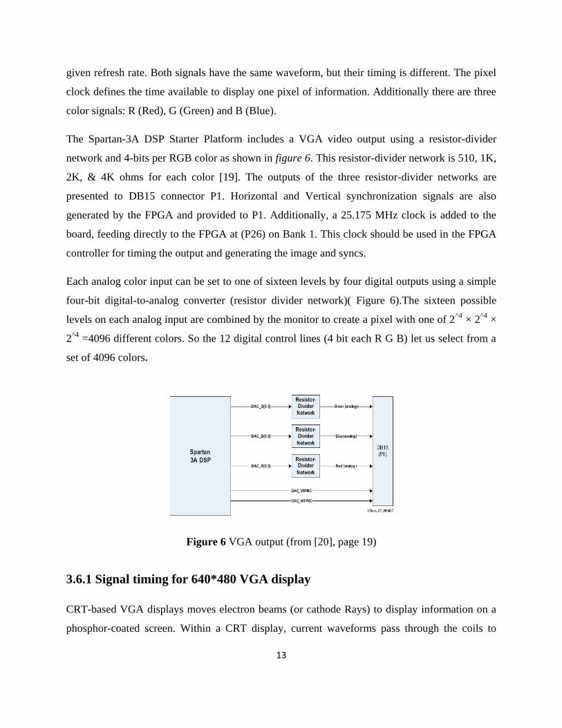
The Spartan-3A DSP Starter Platform includes a VGA video output using a resistor-divider
network and 4-bits per RGB color as shown in figure 6. This resistor-divider network is 510, 1K,
2K, & 4K ohms for each color [19]. The outputs of the three resistor-divider networks are
presented to DB15 connector P1. Horizontal and Vertical synchronization signals are also
generated by the FPGA and provided to P1. Additionally, a 25.175 MHz clock is added to the
board, feeding directly to the FPGA at (P26) on Bank 1. This clock should be used in the FPGA
controller for timing the output and generating the image and syncs.
Each analog color input can be set to one of sixteen levels by four digital outputs using a simple
four-bit digital-to-analog converter (resistor divider network)( Figure 6).The sixteen possible
levels on each analog input are combined by the monitor to create a pixel with one of 2^4
× 2^4
×
2^4
=4096 different colors. So the 12 digital control lines (4 bit each R G B) let us select from a
set of 4096 colors.
Figure 6 VGA output (from [20], page 19)
3.6.1 Signal timing for 640*480 VGA display
CRT-based VGA displays moves electron beams (or cathode Rays) to display information on a
phosphor-coated screen. Within a CRT display, current waveforms pass through the coils to

14
produce magnetic fields that deflect electron beams to transverse the display surface in a raster
pattern, horizontally from left to right and vertically from top to bottom. As shown in Figure 7,
information is only displayed when the beam is moving in the forward direction - left to right
and top to bottom and not during the time the beam returns back to the left or top edge of the
display.
Figure 7 VGA Display Timing (from [20])
3.6.2 Synchronization signal timing
Table 1 640X480 resolution VGA Timing (from [20])

15
Figure 8 VGA Control Timing (from [20])
The VGA controller generates two synchronization signals; the horizontal sync (HS) and vertical
sync (VS) timing signals and coordinates the delivery of video data on each pixel clock.
HS signal marks the start and end of a line and ensure that the monitor displays the pixels
between the left and right edges of the visible screen area. VS signal marks the start and end of a
frame made up of video lines and ensure that the monitor displays the lines between the top and
bottom edges of the visible monitor screen or VS signal defines the refresh frequency of the
display or the frequency at which all information on the display is redrawn.
Table 1 shows the relation between each of the timing symbols for a 640* 480 display using a
25 MHz pixel clock at 60 Hz refresh rate The timing for the sync pulse width (TPW) and front
(TFP )and back porch intervals (TBP) are based on observations from various VGA displays
.Information cannot be displayed during the porch intervals.
3.7 Stepper Motor
Stepper motors are the motors without the commutators. The stepper motor has number of
windings and rotation of the shaft is achieved by sequentially energizing the windings of the
motor. The motor shaft can be locked in position when the windings are energized. The speed at
which the stepper is to be operated is determined by the rate at which the sequence is provided.
However there is a maximum speed at which the motor can be run and beyond that speed the
motor starts loosing the steps and it becomes impossible for the controller to track the position of
the motor shaft. All of the commutation must be handled externally by the motor controller, and
typically, the motors and controllers are designed so that the motor may be held in any fixed
position or rotated in either direction. The direction of rotation depends on which winding is the
"leader" and which is the "follower". The rotation will reverse if the sequence of bits provided is

16
reversed. Stepping motors can be used in simple open-loop control systems; these are generally
adequate for systems that operate at low accelerations with static loads [21, 22]. If a stepper in an
open-loop control system is overtorqued, all knowledge of rotor position is lost and the system
must be reinitialized. Steppers move in small increments usually indicated on the label in
degrees.
3.8 MOSFET
For driving the stepper motor coil we used high current IRF540N N-channel MOSFET. The
MOSFET is a device used to amplify or switch electronic signals. The MOSFET is composed of
a channel of n-type or p-type semiconductor material. A big advantage of MOSFETs for digital
switching is that the oxide layer between the gate and the channel prevents DC current from
flowing through the gate, further reducing power consumption and giving large input impedance.
The insulating oxide between the gate and channel effectively isolates a MOSFET in one logic
stage from earlier and later stages, which allows a single MOSFET output to drive a considerable
number of MOSFET inputs [23]. This isolation also makes it easier for the designers to ignore to
some extent loading effects between logic stages independently. However, the impedance of the
MOSFETs decreases with the increase in the frequency of operation.
Figure 9 Schematic diagram of N-channel Power MOSFET (from [24])
3.9 I2C Interface
The I2C is a multi-master communication protocol developed to connect the low speed
communication devices with motherboard. It uses two bidirectional lines and number of devices
is connected to the line. It uses seven bit address with 16 reserved addresses, thus maximum of
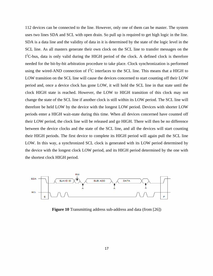
17
112 devices can be connected to the line. However, only one of them can be master. The system
uses two lines SDA and SCL with open drain. So pull up is required to get high logic in the line.
SDA is a data line and the validity of data in it is determined by the state of the logic level in the
SCL line. As all masters generate their own clock on the SCL line to transfer messages on the
I2C-bus, data is only valid during the HIGH period of the clock. A defined clock is therefore
needed for the bit-by-bit arbitration procedure to take place. Clock synchronization is performed
using the wired-AND connection of I2C interfaces to the SCL line. This means that a HIGH to
LOW transition on the SCL line will cause the devices concerned to start counting off their LOW
period and, once a device clock has gone LOW, it will hold the SCL line in that state until the
clock HIGH state is reached. However, the LOW to HIGH transition of this clock may not
change the state of the SCL line if another clock is still within its LOW period. The SCL line will
therefore be held LOW by the device with the longest LOW period. Devices with shorter LOW
periods enter a HIGH wait-state during this time. When all devices concerned have counted off
their LOW period, the clock line will be released and go HIGH. There will then be no difference
between the device clocks and the state of the SCL line, and all the devices will start counting
their HIGH periods. The first device to complete its HIGH period will again pull the SCL line
LOW. In this way, a synchronized SCL clock is generated with its LOW period determined by
the device with the longest clock LOW period, and its HIGH period determined by the one with
the shortest clock HIGH period.
Figure 10 Transmitting address sub-address and data (from [26])

18
4. DESIGN AND IMPLEMENTATION
4.1 System Block Diagram
Figure 11 System Block Diagram

19
4.2 Hardware Implementation
4.2.1 I2C interface
Functional description
The I2C controller module is used to configure C3038 sensor module in different modes as
required by the system. The module takes in control signals from the top level central control
system and configures the image sensor accordingly.
Figure 12 Block Diagram of the I2C module
Implementation
We have implemented this module as a combination of finite state machine and data path model.
Different signals such as SDA and SCL are generated by different processes and a central finite
state machine controls those processes. The module keeps SCL and SDA high if its reset pin is
high. Once reset pin is low it waits for a start signal which if asserted it prepares to send data
provided in config_reg input. It first checks the status of the SDA and SCL signals to get access
of the communication line. If both SDA and SCL are high then the lines can be accessed for
communication. This module is used by the system to bring the CMOS image sensor in the
desired configuration mode.
Simulation
A snapshot of post map simulation of I2C module

20
Figure 13 Simulation of I2C module
This module has not been used yet because we have used the CMOS sensor in default mode.
However, we have tested the module using different simulation levels so that it can be
implemented in real hardware whenever required.
4.2.2 Framegrabber
Figure 14 Block Diagram of the framegrabber module
Functional description
The framegrabber module interfaces camera with the rest of the system. This module uses
signals pclk, href, and vsync of the camera to infer which pixel data is present in Y and UV data
bus of the camera at any instant. It generates pixel_count and line_count to give the address of
the corresponding pixel data it sends out in data (16-bit) bus. Other modules can take the valid

21
data when data_valid output is asserted. For every new pixel data framegrabber issues a
data_valid signal for a single clock cycle.
Implementation
We have implemented this module as a fsm. This module starts working only when start signal is
asserted for at least one clock cycle. It then waits until a new frame starts with vsync going high.
Every new pixel is latched into data out when pclk is high. Pixel_count is increased and
data_valid signal is asserted for a single clock cycle. Line_count increases for every new line and
pixel_count is reset to zero. Thus pixel_count gives the position of pixel on any line. It continues
until vsync goes high again characterizing the start of another frame.
Simulation snapshot
Since the camera was not available until the later stage of the project, we designed a VHDL test
bench that simulated the signals produced by the image sensor. This virtual image sensor was
used to test the functioning of the modules that depended upon the signals coming from the
image sensor.
Figure 15 Simulation of the framegrabber module
ChipScope was used to check the working of the module in actual hardware.

22
Figure 16 Real-time signal capture of the framegrabber module
4.2.3 UV_separator
Figure 17 Block Diagram of the UV_separotor
Functional description
This takes in data from framegrabber module along with the data_valid signal. It separates u and
v data from uv data bus. It takes in Y data to synchronize it with the separated u and v data. Thus
the module takes in YUV data in 16-bit and generates YUV data in 24-bit.
Implementation
This is a fsm that basically transits between two states of assigning u and v data. U and V data
from framegrabber comes in alternately in a single bus. The module keeps track of U and V data
and outputs these data in separate 8-bit buses. When V data is being assigned in for_v state, a
register is used to output previous U data. Similarly, when U data is being assigned in for_u
state, another register is used to output previous V data. Signal data_valid_out is simply a single

23
clock delayed version of data_valid_in. Thus for every two data_valid_out signal, either
u_separated or v_separated will have the same value.
Simulation snapshot
Figure 18 Simulation of the UV_separator module
ChipScope was used to check the working of the module in actual hardware.
Figure 19 Real-time signal capture of the UV_separator module
4.2.4 Color_recognition
Functional description
The module takes in ranges of y, u and v values and counts total number of pixels lying within
the given ranges in each frame. It assumes higher value of the range is stored in upper byte (15 to
8) and lower value in lower byte (7 to 0) for y, u and v ranges. This gives total pixels lying
within the range in between every new_frame signal pulse.
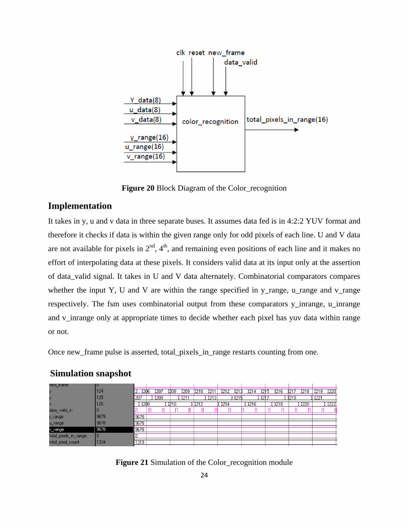
24
Figure 20 Block Diagram of the Color_recognition
Implementation
It takes in y, u and v data in three separate buses. It assumes data fed is in 4:2:2 YUV format and
therefore it checks if data is within the given range only for odd pixels of each line. U and V data
are not available for pixels in 2nd
, 4th
, and remaining even positions of each line and it makes no
effort of interpolating data at these pixels. It considers valid data at its input only at the assertion
of data_valid signal. It takes in U and V data alternately. Combinatorial comparators compares
whether the input Y, U and V are within the range specified in y_range, u_range and v_range
respectively. The fsm uses combinatorial output from these comparators y_inrange, u_inrange
and v_inrange only at appropriate times to decide whether each pixel has yuv data within range
or not.
Once new_frame pulse is asserted, total_pixels_in_range restarts counting from one.
Simulation snapshot
Figure 21 Simulation of the Color_recognition module

25
ChipScope was used to check the working of the module in actual hardware.
Figure 22 Real-time signal capture of the Color_recognition module
4.2.5 Edge Detector
This module consists of a moving window and a sobel mask operator.
I) Moving_window
Figure 23 Block Diagram of the moving_window module
Functional description
The moving window creates an effect of sliding through the pixels in a frame, covering each
time a window of 3X3 matrix. For each pixel in a frame, it provides surrounding eight pixel data
upon which a window operator may be applied to give a corresponding value for that pixel based
on the operation. In our case the output data of the moving window is used by sobel mask
operation. Y data from the camera is the input d_in for this module.

26
Implementation
For the pipelined implementation of edge detection algorithm all the pixels in the moving
window operator must be accessed at the same time for every clock. In order to access all the
pixels in a moving window system, we implemented a design explained in [27]. FIFO buffers
create the effect of moving an entire window of pixels through the memory for every clock
cycle. We used a FIFO core provided by the Xilinx in the moving window module [28]. A FIFO
consists of a block of memory and a controller that manages the traffic of data to and from the
FIFO. The availability of multi-port BRAM in the Xilinx Spartan 3A DSP FPGA helps in
achieving the read and write operations of the BRAM in the same clock cycle [29]. This allows a
throughput of one pixel per clock cycle. For a 3x3 moving window two FIFO buffers are used.
Block Rams were used to generate two FIFO cores of size (352 – 3 =) 349 bytes. To access all
the values of the window for every clock cycle the two FIFO buffers must be full. Figure 24
shows the architecture of the 3x3 moving window. For every new data_valid pulse from
framegrabber module, y data is fed and placed into the register R9. The contents of the window
are shifted to the left, with the leftmost member being added to the tail of the FIFO. The top left
pixel is disposed after the computation on the pixels is completed, since it is not used in future
computation.
Figure 24 The architecture of the 3x3 moving window

27
Simulation snapshot
Figure 25 Simulation of the Moving_window module
II) Sobel edge calculation
Figure 26 Block Diagram of the sobel_edge module
Functional description
This stage calculates the vertical and horizontal gradients using 3x3 Sobel masks. The input to
the horizontal and vertical gradient calculation is taken from the output of moving window.
Implementation
Since the design is pipelined, calculation starts once the 2 FIFO buffers are full. That is, the
output is produced after a latency of twice width of image plus two (2*width +2) cycles. For the
width of 352 pixels, the latency is 706 cycles.

28
Figure 27 Hardware implementation of Sobel Edge Detection
The gradient calculation introduces negative numbers. Here negative numbers are handled using
numeric_std package. In this design, the calculated gradient is represented by 10 bits. Two
gradient values are calculated for each pixel, one for vertical and other for horizontal. The
multiplication by two is achieved by a simple shifting of one bit to left. The 10 bits of vertical
gradient and the 10 bits of the horizontal gradient are compared with the input threshold value.
The outputs of the comparators are concatenated to produce two bits that represent presence or

29
absence of horizontal and vertical edge for the corresponding pixel. The calculation takes up
around 18 ns and therefore it is faster than data input rate from the image sensor.
Simulation snapshot
Figure 28 Simulation of the Sobel_edge module
4.2.6 Video display system
The main objective of the display system is to display the real time video coming from the digital
image sensor module C3038, which is useful for the analysis and debugging purposes of the
project. Figure 29 shows the higher level design of the video display system.
The main constituent blocks are the memory controller, simple dual port RAM, Y to RGB assign
module and VGA controller module. Memory controller is implemented in hardware module that
governs the timing and synchronization of writing the pixel data coming from the frame grabber
module to the on chip BRAM and it also governs reading the stored pixel data from BRAM where
it is stored. After reading the camera luminance(Y) data from the BRAM ,the 4 MSBs of the Y
are assigned to the RGB values which will produce the video in grayscale format because the
luminance(Y data) only contains the brightness information not the color. Ultimately the VGA
controller maps the time domain RGB data into the corresponding special domain RGB data with
the help of the two synchronization signals Vsync and Hsync.
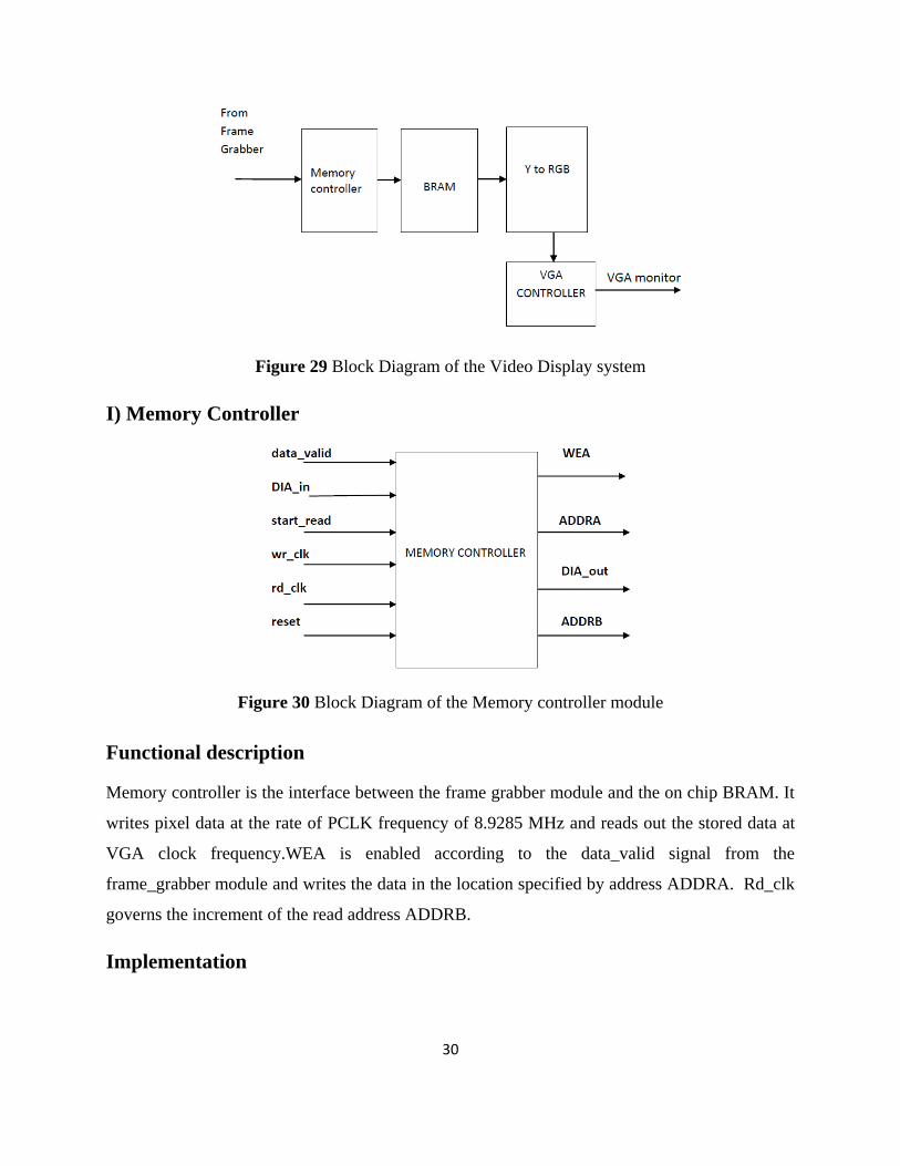
30
Figure 29 Block Diagram of the Video Display system
I) Memory Controller
Figure 30 Block Diagram of the Memory controller module
Functional description
Memory controller is the interface between the frame grabber module and the on chip BRAM. It
writes pixel data at the rate of PCLK frequency of 8.9285 MHz and reads out the stored data at
VGA clock frequency.WEA is enabled according to the data_valid signal from the
frame_grabber module and writes the data in the location specified by address ADDRA. Rd_clk
governs the increment of the read address ADDRB.
Implementation

31
The pixel data from the camera is provided at the rate of 8.9285 MHz that is PCLK of the camera
has pixel timing of 112ns at the rate of 50 frames per second in the progressive scan technique
[30]. The pixel timing information is observed from the logic analyzer but for the standard
640*480 display resolution at 60Hz refresh rate the standard clock is 25.175 MHz. Nevertheless
our objective is to display the real time video data. Due to the constraints imposed by the slow
data transfer rate of camera and fast data acceptance rate of VGA monitor, it is not possible to
give out the camera pixel data directly to the VGA monitor. So it is convenient to use the
memory for storing the pixel data for some reasonable time obtained from the timing calculation.
The use of the dual port RAM with two independent clocks are advantageous for our case, one
port is used for writing the pixel data and another for reading the same but with independent
clock speed.
Camera needs 64.1us (obtained from logic analyzer) to write the single line (with 352 pixels) in
the BRAM memory and for 640 *480 resolution VGA controller needs 31.77 us to scan a single
line in VGA monitor[31]. Since the VGA clock speed is very fast compared to speed of the
camera, computations show that if we start reading the data from the block RAM only after the
writing 4 lines of data from the image sensor module then the writing the data provided by
camera and reading the data for VGA will be synchronized. So additionally we need to plot the
same pixel twice in a line, so the resulting effect will be zoomed in format of video. But with this
algorithm we will be able to show only the 320 of 352 pixels of each line and 240 of 288 line of
each frame.
The Dual-Port Block Memory LogiCORE module provided by Xilinx uses on-chip FPGA block
memory resources to implement RAM functions. The core is fully synchronous and supports
three write mode options: Read-After-Write, Read-Before-Write, and No-Read-On-Write. Data
widths ranging from 1 to 256 bits and memory depths from 2 to 4M words can be supported
[29], depending on the selected target device family. The two ports of the Dual Port core are
completely independent.

32
Figure 31 Simple dual port RAM core schematic symbols
Simulation snapshot
Figure 32 Simulation of the Memory controller module
II) VGA controller
Figure 33 Block Diagram of the VGA_controller module
Functional description
It is an interface between Y to RGB converter and VGA monitor. Whenever the 8 bit luminance
data (Y data) is read from memory and converted to corresponding RGB by Y to RGB converter
33
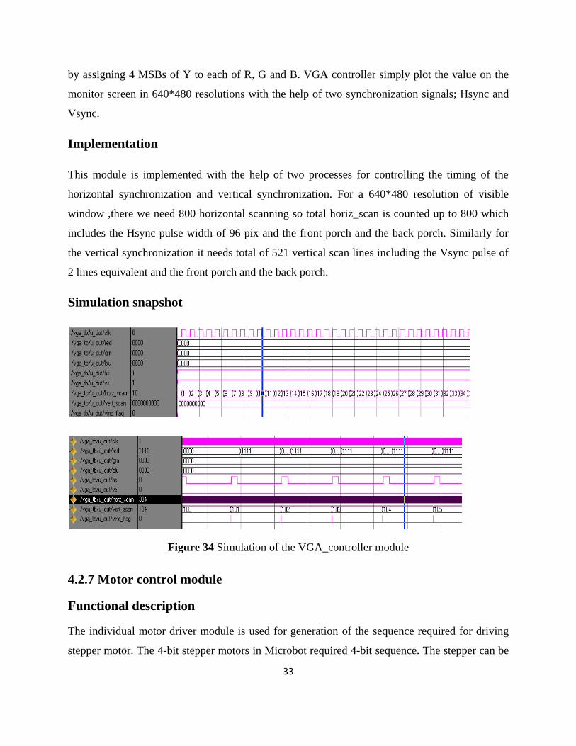
by assigning 4 MSBs of Y to each of R, G and B. VGA controller simply plot the value on the
monitor screen in 640*480 resolutions with the help of two synchronization signals; Hsync and
Vsync.
Implementation
This module is implemented with the help of two processes for controlling the timing of the
horizontal synchronization and vertical synchronization. For a 640*480 resolution of visible
window ,there we need 800 horizontal scanning so total horiz_scan is counted up to 800 which
includes the Hsync pulse width of 96 pix and the front porch and the back porch. Similarly for
the vertical synchronization it needs total of 521 vertical scan lines including the Vsync pulse of
2 lines equivalent and the front porch and the back porch.
Simulation snapshot
Figure 34 Simulation of the VGA_controller module
4.2.7 Motor control module
Functional description
The individual motor driver module is used for generation of the sequence required for driving
stepper motor. The 4-bit stepper motors in Microbot required 4-bit sequence. The stepper can be

34
driven in half step or in full step. However the module generates the sequence in half step which
increases the torque and also reduces the jerky motion.
Figure 35 Block Diagram of the Motor Driver module
Implementation
We implemented the module (figure 35) as a combination of finite state machine and data path
model. Different signals such as ready control and drive_signals are generated by different
processes and a central finite state machine controls those processes. Upon reset the output
signals are set to zero logic so that all the windings of the stepper motor will be de-energized.
Once reset pin is low it waits for a start signal which if asserted it generates the drive signal
sequence according to the data in the speed_pin, no_of_degrees and direction signals and
indicates busy until the required no of degrees is completed. After the completion it issues
completed signal. Then it again asserts the ready signal to indicate readiness to accept next
command.
To control six different motors of Microbot we created six instances of the stepper driver module
(Figure 36). The stepper driver module acts as a component and the motor controller module
uses six such components. Thus all the components can work in parallel which is an advantage
of FPGA over other microprocessor based system. The central controller controls the operation
all the stepper driver module. The stepper controller module acts as an interface between the

35
MicroBlaze system and different motor driver modules. It gets the necessary information such as
start, task to be performed, no of degrees to be rotated and also informs the MicroBlaze system
about the completion of the task, indication of busy signal.
Figure 36 Block diagram of stepper motor controlling
Simulation snapshot
Figure 37 Simulation of the stepper motor controller

36
4.2.8 Motor Driver Circuit and PCB fabrication
I) Driver circuit
We designed the driver circuit with necessary protection system and sufficient current driving
capacity. The designed circuit is shown below
Figure 38 Driver circuit for driving stepper motor coil
Components used in the driver circuit.
Resistors:
o R1=330 ohm.
o R2 = 2.2Kohm
o R3 = 2.2Kohm
o R4=2.2Kohm
Q1 is optoisolator.
Diodes D1, D4 are 1N4007.
Diodes D2,D3 are 15 volt zener diode.
Diodes D5 and D6 are leds.
Q2 is IRF540N n-channel MOSFET.
B1 is 12V Supply for motor.
GND1 FPGA ground.
GND2 MOTOR supply ground.
37
Operation
The MOSFET normally remains off due to the pull down of the gate voltage by the series
connection of the resister R3 and led D5. When the input from the FPGA is of high logic the
diode of the optoisolator is turned on biasing the transistor. Thus the gate voltage is increased
turning on the MOSFET. In this way the winding of the stepper motor is energized. When input
is low the MOSFET is turned of resulting in de-energizing of the winding.
The MOSFET is highly sensitive to high voltage and gets damaged if the gate to source voltage
exceeds 20 volt. So for protection we used the 15 volt zener diode. The protection from high
reverse voltage is obtained by using diode D1 and D4.
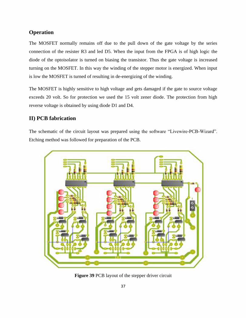
II) PCB fabrication
The schematic of the circuit layout was prepared using the software “Livewire-PCB-Wizard”.
Etching method was followed for preparation of the PCB.
Figure 39 PCB layout of the stepper driver circuit

38
4.3 SOFTWARE SPECIFICATION
4.3.1 Edge Detection
We tested some of the edge detection masks in software using visual C++ using the image of
objects taken from cell phone camera [1.3 megapixel camera from Nokia 3110c]. They are
Prewitt sobel krisch
-1 0 1 -1 -1 -1 -1 -2 -1 -1 0 1 -3 -3 -3 5 -3 -3
-1 0 1 0 0 0 0 0 0 -2 0 2 0 0 0 5 0 -3
-1 0 1 1 1 1 1 2 1 -1 0 1 5 5 5 5 -3 -3
Figure 40 Horizontal and vertical operators
The calculation of central pixel value involves sliding a mask over the image repeatedly
performing sum of the products calculations between the mask and the values covered as shown
below:
Figure 41 Image and Convolution Mask
For example a22 can be calculated by
a22 = a11*W11 + a12*W12 + a13*W13 + a21*W21 + a22*W22 + a23*W23
+ a31*W31 +a32*W32 + a33*W33
39
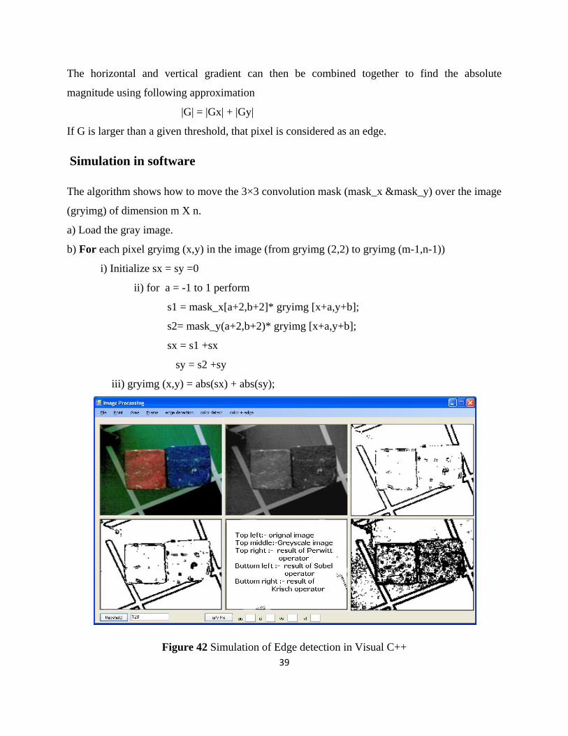
The horizontal and vertical gradient can then be combined together to find the absolute
magnitude using following approximation
|G| = |Gx| + |Gy|
If G is larger than a given threshold, that pixel is considered as an edge.
Simulation in software
The algorithm shows how to move the 3×3 convolution mask (mask_x &mask_y) over the image
(gryimg) of dimension m X n.
a) Load the gray image.
b) For each pixel gryimg (x,y) in the image (from gryimg (2,2) to gryimg (m-1,n-1))
i) Initialize sx = sy =0
ii) for a = -1 to 1 perform
s1 = mask_x[a+2,b+2]* gryimg [x+a,y+b];
s2= mask_y(a+2,b+2)* gryimg [x+a,y+b];
sx = s1 +sx
sy = s2 +sy
iii) gryimg (x,y) = abs(sx) + abs(sy);
Figure 42 Simulation of Edge detection in Visual C++

40
Choice of masks
While choosing the mask it must fulfill some requirements. Masks should have noISE
suppression characteristics and easy to implement in hardware. After the experimentation and
reviewing various literatures regarding edge detection [17, 32, 33, 34, 41, 42], we decided to use
one of the most popular operator – Sobel operator. In this operator the arithmetic operation
involves only addition, subtraction and shifting which can be efficiently implemented in FPGA.
4.3.2 Object Detection
The result of edge detection is the binary image. We performed Hough Transformation to extract
the parameters of required line segments to determine whether the object is rectangular cube or
not.
We used Hough Transformation because it is simple and fulfills our objectives. Besides that, it is
invariant to the orientation of the object
Simulation/Implementation
The Hough transform was first tested in Matlab and then implemented in MicroBlaze. Even
though Matlab has some built-in Hough functions, these functions were not used. The pseudo
code of the Hough implementation is given below:
a) Load binary image containing edge.
b) For all pixels in the image
If the pixel (x, y) is an edge
For the theta angles-90 to 90 degrees
Calculate rho for the pixel (x, y) and the angle (theta)
Increment that position (rho, theta) in the accumulator
c) Examine the votes of the accumulator cells for high edge concentrations. The reasonable lines
are detected by locating local maxima the Hough space. We have used 5x5 window to find local
maxima.
Now we have (ρ1, θ1), (ρ2, θ2), (ρ3, θ3) and (ρ4, θ4) for four sides of rectangular cube. The
parallel sides have same θ where as difference between θ of adjacent sides is 90 degrees. Using

41
appropriate threshold limits we can detect cubes from spheres. For spheres there are no such
lines.
Hough Transformation requires floating point operations. To speed up the calculation, we have
used sine/cosine lookup table and floating point unit of MicroBlaze instead of software routines.
Simulation results
For case of sphere there as no such lines which fall on our threshold.
Figure 43 Simulation of Object Detection in Matlab

42
4.3.3) Color Detection
The detection of color is done from the chrominance data. Cr ranges from cyan to red where as
Cb ranges from yellow to blue. The ranges are shown in graph below:-
Figure 44 YUV range (from [35], page 5)
For detecting red color, Cr value must exceed lower limit above 128 (say 160) and Cb value
must be within the certain range around 100 to 150.The choice of threshold is determined by
tuning which depends upon how pure the particular color is. For detecting white and black color,
we must go for Y as Cr and Cb values for this color is around 128.
Simulation in visual C++
Figure 45 Simulation of Color detection in Visual C++

43
5. RESULTS
We have successfully demonstrated the recognition of objects of three different colors: Red,
white and black. We checked the range in which the sensor provided YUV data for different
colors. This image sensor did not give good response to blue and green.
Edge detection was implemented in hardware. A distinctive advantage of the parallel structure in
FPGA is shown with this implementation. Here is the comparison of the implementation of sobel
edge in hardware and software.
Time taken by Edge detector
hardware in FPGA using 125
MHz system clock
Time taken for Edge detection in
software using 2 GHz Pentium 4
processor
Sobel Edge detection in
one direction
19ns 153.6 ns
Sobel Edge detection in
vertical and horizontal
direction
19 ns 211.4 ns
Table 2 Comparison between hardware and software to determine whether the given pixel is
edge or not
We could not successfully implement following, in a complete system due to time limitation
thanks to the unprecedented power outage of 12-16 hours daily in our country for the last four
months of the project.
i) Integration of Object detection from MicroBlaze using edge data provided by the edge
detector.
ii) Displaying of video data from C3038 to the VGA monitor.

44
6 CONCLUSIONS AND RECOMMENDATION
6.1 Conclusions
The system at present recognizes objects of red, white and black. The complete system stands as
a starting base platform for more complex vision tasks and planning of control actions for
autonomous robots. This system is a first step towards research and development of FPGA based
robots with real-time vision capability that can have wide range of applications like unmanned
ground vehicle (UGV), unmanned Air vehicle (UAV) etc in IOE. The results show that a choice
of hardware and software for the implementation of image processing algorithms provided by
this approach enables possibility of greater optimization for the designed system.
6.2 Recommendations
Designing and integrating a complete hardware and software system in a vendor specific FPGA
requires a significant amount of experience in using the development tools provided by the
vendor. SoC designs have a high learning curve for the software tools used. Instead of waiting
for the designs to complete and test them, starting with the reference designs and examples and
getting used to with the development tools early in the design process is important. Xilinx’s ISE
and EDK contain quite a few bugs and if one gets stuck with some strange problems, a
possibility of the problem with the tools themselves should not be ruled out. Since testing a
complete integrated system is quite cumbersome, extensive testing and verification of the
modules before system integration is very important.
Programming in MicroBlaze and designing user peripherals for the processor in hardware should
not be seen in an isolated manner. Any aspect of the system must be considered with its
advantages and disadvantages for the possible design in either hardware or software.
45
REFERENCES
1 Makimoto T., Doi T.T., “Chip Technologies for Entertainment Robots”; International Electron
Devices Meeting, pp. 9-16, December 2002.
2 Anil Raj Khadka,Nusb Karmacharya,Shankar Raj Uprety; “Machine Vision for Multi agent
Robotics”; IOE,2004
3 José Fernández-Pérez, Francisco J. Sánchez-Fernández, Ricardo Carmona-Galán.Performance;
“Evaluation and Limitations of a Vision System on a Reconfigurable/Programmable Chip”;
Journal of Universal Computer Science, vol. 13, no. 3 (2007), 440-453
4 Dylan Muir and Joaquin Sitte Smart Seeing cheaply; “Flexible vision for small devices”;
Devices Laboratory, Centre for Information Technology Innovation, Faculty of Information
Technology, Queensland University of Technology, 2 George Street, Brisbane, QLD 4001
AUSTRALIA
5 Shinichi Hirai, Masakazu Zakoji, Akihiro Masubuchi, and Tatsuhiko Tsuboi , Ritsumeikan
Kusatsu ;“FPGA-Based Realtime Vision System” ; Journal of Robotics and Mechatronics
Vol.17 No.4, 2005
6 Ridha Djemal, Didier Demigny and Rached Tourki; “A Real-time Image Processing with a
Compact FPGA-based Architecture”; Faculte des Sciences de Monastir, Avenue de
l’Environnement 5019 Monastir, Tunisie Laboratoire ETIS, ENSEA Universite Cergy
PontoISE, France; Journal of Computer Science 1 (2): 207-214, 2005 ISSN 1549-3636
7 Wade S. Fife and James K. Archibald ; “Reconfigurable On-Board Vision Processing for
Small Autonomous Vehicles”; Hindawi Publishing Corporation;EURASIP Journal on
Embedded SystemsVolume 2007, Article ID 80141, pp. 14
8 J. Bruce, T. Balch and M. Veloso, “Fast and Inexpensive Color Image Segmentation for
Interactive Robots”, IROS 2000, San Francisco, 2000, pp. 2061 – 2066.
9 http://www.questechzone.com/czone.htm

46
10 “EDK Concepts, Tools and Techniques” ;
www.xilinx.com/support/documentation/sw_manuals/EDK_ctt.pdf
11 “FPGA-Based Control: Millions of Transistors at Your Command“;National Instruments
Developer zone; http://zone.ni.com/devzone/cda/tut/p/id/3357
12 http://en.wikipedia.org/wiki/Field-programmable_gate_array
13 http://en.wikipedia.org/wiki/System-on-a-chip
14 “MicroBlaze Processor Reference Guide”; UG081 (v8.0);
www.xilinx.com/support/documentation/sw_manuals/mb_ref_guide.pdf
15 Keith Jack ;”Video demystified, A handbook for the digital engineer”;3rd
edition;
page 18
16 http://www.csm.uwe.ac.uk/~irjohnso/coursenotes/uqc146/uqc146s1-02-aa2-1.pdf
17 Dana H. Ballard and Christopher M. Brown ; “Computer Vision” Prentice Hall 1982
18 Hamblen, James O., Hall, Tyson S., Furman, and Michael D.; “ Rapid Prototyping of
Digital Systems SOPC Edition”; Springer 2008
19 “Spartan-3A DSP Starter Platform User Guide”; http://www.xilinx.com/support/
documentation/boards_and_kits/ ug454_sp3a_dsp_start_ug.pdf
20 “Displaying Graphics Through the VGA Interface “;
http://homepage.hik.se/staff/tkama/Datorsystem/lab/Lab_vga.pdf
21 http://en.wikipedia.org/wiki/Stepper_motor
22 “Stepper Motor Basic”; www.solarbotics.net/library/pdflib/pdf/motorbas.pdf
23 http://en.wikipedia.org/wiki/MOSFET
24 “Power MOSFET Basics”; http://www.irf.com/technical-info/appnotes/mosfet.pdf

47
25 “THE I 2C-BUS SPECIFICATION”; Ver 2.1;Philips Semiconductors;
http://i2c2p.twibright.com/ spec/i2c.pdf
26 “I2C Bus START and STOP condition”;
http://www.esacademy.com/faq/i2c/busevents/i2cstast.htm
27 Venkateshwar Rao Daggu and Muthukumar Venkatesan “; Design and Implementation of an
Efficient Reconfigurable Architecture for Image Processing Algorithms using Handel-C”;
Department of Electrical and Computer Engineering University of Nevada;Las Vegas
28 http://www.xilinx.com/support/documentation/ip_documentation/fifo_generator_ds317.pdf
29 www.xilinx.com/support/documentation/ip_documentation/dp_block_mem.pdf
30 “OV6630/OV6130 Specification”;
http://www.digchip.com/datasheets/parts/datasheet/341/OV6630.php
31 www.xess.com/appnotes/an-101204-vgagen.pdf
32 Rafael C. Gonzalez and Richard E. Woods; “Digital Image Processing”; second
edition,2002 Prentice Hall
33 Anil K. Jain; “Fundamentals of Digital Image Processing “ ;Pearson Education inc,1989
34 Dwayne Phillips; “Image processing in C “; second edition, 2000
35 Dawit Bekele ,Han Liang,Alison Leonard, Edward Mung; “Color Tracking Robot”;
http://www1.cs.columbia.edu/~sedwards/classes/2006/4840/reports/VGLR.pdf
36 http://www.cs.uml.edu/~lkyewook/hough/APPLICATION%20OF%20THE%20
HOUGH%20TRANSFORM%20V1.9.pdf
37 C. T. Johnston, K. T. Gribbon, D. G. Bailey; “Implementing Image Processing Algorithms on
FPGAs ”; Institute of Information Sciences & Technology, Massey University Private Bag
11- 222, Palmerston North, New Zealand
38 Christopher T. Johnston, Kim T Gribbon, Donald G. Bailey; “FPGA based Remote Object

48
Tracking for Real-time Control”; Institute of Information Sciences and Technology, Massey
University, Palmerston North, New Zealand
39 C.T. Johnston, D.G. Bailey, K.T. Gribbon; “Optimisation of a colour segmentation and
tracking algorithm for real-time FPGA implementation”; Institute of Information Sciences
and Technology, Massey University, Palmerston North
40 A. S. Bishell, D.G. Bailey, P. Lyons; “Designing the Control Architecture forAlgorithm
Specific Custom Processors on FPGAs”; Institute of Information Sciences & Technology,
Massey University Private Bag 11-222, Palmerston North, New Zealand
41 www.cse.cuhk.edu.hk/~lyu/staff/SongJQ/Edge.ppt
42 “Comparison of Edge Detectors”; marathon.csee.usf.edu/~sarkar/PDFs/heath- cviu.pdf
43 http://research.microsoft.com/en-us/um/people/zhang/Papers/ZhangHeDSP07.pdf
44 Anthony Edward Nelson; “Implementation Of Image Processing Algorithms On FPGA
Hardware”;
ww3.isis.vanderbilt.edu/publications/archive/Nelson_T_0_0_2000_Implementa.pdf
45 I. Navarro Oiza; “Digital Camera Interface”; http://www.robozes.com/inaki/dproject/
49
APPENDIX A

50

51
APPENDIX B

52