trinity college dublin applied physics research group · pdf file1 trinity college dublin...
TRANSCRIPT

1
Trinity College Dublin
Applied Physics Research Group
Biennial Report 2010 – 2011
Address: Prof Igor Shvets
Centre for Research on Adaptive Nanostructures and Nanodevices (CRANN) and School of Physics Trinity College Dublin 2 Ireland
Tel: + 353 1 896 1653 Fax: +353 1 671 1759
Internet: http://www.tcd.ie/Physics/applied-physics/ E-mail: [email protected] [email protected] This report can be downloaded from: http://www.tcd.ie/Physics/applied-physics/Publilcations/biennial-reports/

2
The Group
From Left to right Back row: Rafael Ramos, Floriano Cuccureddu, Dr Victor Usov, Dr Sumesh Sofin, Michael Sexton, Sundar Raja Vadapoo, Savas Ulucan, Dr Karsten Fleischer, Ruggero Verre, Dr Guido Mariotto, Olaf Lübben, Warren O'Neill, Brendan Doherty, Kenneth Gotlieb. Front row: Ciarán McEvoy, Cormac Ó Coileain, Dr Sunil Arora, Prof Igor Shvets, Paul McElligott, Dr Han Chun Wu, Barry Heffernan, Joanna Baginska, Vincy Gheeraraughese

3
Contents 1. Preface .......................................................................................................................................... 4
2. Atomic Terrace Low Angle Shadowing (ATLAS)............................................................................... 6
3. Group Members ............................................................................................................................ 7
3.1 Group Leader ........................................................................................................................... 7
3.2 Postdoctoral Researchers......................................................................................................... 7
3.3 Postgraduate Students ............................................................................................................. 7
3.4 Administration ......................................................................................................................... 7
3.5 Academic Visitors and Examiners ............................................................................................. 7
4. Centre for Research on Adaptive Nanostructures and Nanodevices (CRANN)................................. 8
5. Research Infrastructure ................................................................................................................. 9
5.1 Group Facilities ........................................................................................................................ 9
5.2 CRANN Facilities include: ....................................................................................................... 11
6. Selected Example of Experimental Results ................................................................................... 13
6.1 Scanning Tunnelling Microscopy and Spectroscopy Sub-group ............................................... 13
6.2 Thin Film ................................................................................................................................ 22
6.2.1 Step Bunching (ATLAS) .................................................................................................... 22
6.2.2 Planar Nanowire Arrays (ATLAS) ...................................................................................... 28
6.2.3 Thin Films ........................................................................................................................ 30
6.2.4 Plasmonic Nanoparticles Arrays (ATLAS).......................................................................... 44
6.3 Cleaner Energy Laboratory ..................................................................................................... 48
7. Commercialisation ....................................................................................................................... 50
8. Group Dissemination ................................................................................................................... 52
8.1 Peer Review Publications ....................................................................................................... 52
8.2 Conference Oral Presentations .............................................................................................. 54
8.3 Conference Poster Presentations ........................................................................................... 56
8.4 Awards .................................................................................................................................. 58
9. Research Students Graduated...................................................................................................... 59
9.1 PhD ........................................................................................................................................ 59
9.2 MSc ....................................................................................................................................... 59

4
1. Preface
Dear Colleagues and Friends,
I am happy to present the first report of the Applied Physics Research Group, School of Physics, Trinity College Dublin (TCD). It covers the period January 2010 to December 2011.
The Applied Physics Research Group specialises in materials research, especially the study of surfaces and interfaces of materials. The group is a recognised expert in conducting oxides and a particular world leader in magnetite (Fe3O4). The most recent research theme initiated by the group is in the area of transparent conductors (mainly oxides) for energy and optoelectronic applications. This is driven by our Cleaner Energy Laboratory sub-group.
I will briefly mention a few highlights of our research results for 2010-2011. Recently we focused our STM research on C60 layers deposited on molybdenum and tungsten oxide surfaces. We observed the self-assembly and ordering of C60 on the WO2/W (110) surface, in which the molecules form a close-packed hexagonal structure. Using Low Temperature STM we were able to resolve molecular orbitals within individual C60 molecules. We detected nano-motion in individual C60 molecules, such as rotation, spinning and switching between different orientations and also observed a kinetic transition in thin films of C60 which occurred at 220 K. We obtained fascinating STM images of spinning C60 molecules. The spinning could be suppressed by reducing the temperature of the system. All of our C60 experimental data was supported by our DFT modelling of the same system.
During this period we initiated plasmonic research using our proprietary Atomic Terrace Low Angle Shadowing (ATLAS) technique. In the ATLAS technique, a vicinal substrate is formed with atomic terraces and the material is deposited at a grazing angle. ATLAS is a powerful bottom-up method for the growth of planar nanowire arrays. The versatility of ATLAS is further enhanced by the fact the technique is not material specific. We have developed our ATLAS technique to grow aligned nanoscale long chains of various metals such as silver, gold, iron, copper and nickel. We have investigated the plasmonic response of aligned arrays of nanoparticles of noble metals grown on vicinal Al2O3 substrates. Using Reflection Anisotropy Spectroscopy (RAS) we studied in-situ the optical anisotropy of the nanoparticle arrays in the visible region of the spectrum. The RAS spectral response has a strong peak due to plasmon resonance. The wavelength of the spectral peak is defined by the thickness of the layer deposited as this sets the nanoparticles size and separation. We were able to tune the optical properties of the nanoparticle arrays through control of the ATLAS growth conditions, such as the deposition angle and the layer thickness. The position of the plasmonic peak of the array could be tuned to cover the entire visible spectrum range. We developed a computational model to complement our experimental findings. The computational model agrees well with the experimental results and takes into account the plasmonic properties of single nanoparticles and also the dipole-dipole interaction between the adjacent nanoparticles in the array. We have progressed this work, involving probing the out-of-plane optical response of the plasmonic nanostructures using spectroscopic ellipsometry. From the ellipsometry data we could extract an anisotropic surface excess function (ASEF), whose properties depend only on the dielectric function of the nanoparticle layer. This work would not have been possible without our ATLAS system.
Our ATLAS work is also the backbone of our investigations into the mechanisms of step bunching on vicinal substrates. Vicinal substrates are essential to the ATLAS technique as the atomic steps and terraces provide the shadowing necessary to form the nanostructures. We have invested much effort into developing mechanisms to form suitable vicinal substrates and understanding the physics behind step bunching. To this end we have developed an experimental method to isolate the effects of electromigration in the dynamics of the step bunching process on Si (111) through separate control over the temperature and in-plane applied electric field. The application of an electric field at constant temperature allows greater control over the step bunching process and allows us to fabricate substrates for our ATLAS nanowire growth. By separating the applied electric field and temperature during the step bunching process we have been able to investigate the effect of the electromigration field on the onset of antiband formation on step bunched surfaces. We advanced the state-of-the-art in terms of the

5
understanding of the step bunching process and have elucidated the critical electromigration fields necessary to initiate the step bunching process.
We have also had success in developing a novel p-type transparent oxide semiconductor. The new p-type Transparent Conducting Oxide (TCO) was obtained from well known but poorly conducting chromium oxide (Cr2O3). By co-doping this oxide with magnesium and nitrogen, both the transparency of the oxide, and its conductivity improved significantly. Work is ongoing on this material to understand the exact doping mechanism and the locations of the dopants in the oxide crystal structure. Finding new p-type TCO materials with good conductivity and transparency is important for several applications, such as solar cells and organic light emitting diodes (OLED). We are very excited about this work and have ideas on expanding this approach to other materials.
During the period of this report three students from the group successfully defended their PhD thesis, while two students obtained MSc degrees and departed for industrial positions, in Ireland and overseas. Six new PhD students joined the group: Brendan Bulfin, Askar Syrlybekov, Olzat Tokhtarbaiuly, Oral Ualibek, Leo Farrell and Ozhet Mauit. Leo and Brendan are both graduates of Trinity College Dublin.
Our group saw the departure, in February 2012 of a Postdoctoral Researcher, Dr Rafael Ramos to the University of Zaragoza, Spain to the group of Prof. M. R. Ibarra. Our former PhD student and one of our key researchers, Dr. Sumesh Sofin will be taking up a prestigious faculty position at the Sultan Qaboos University in Muscat, Oman. This is well funded position and Sumesh will face the challenge of setting up a new experimental research group in this rapidly growing region of the world. We wish him well in this new exciting endeavour.
Two of our former PhD students and research fellows for over 10 years, Dr. Roman Kantor and Dr. Guido Mariotto, bravely decided to leave the comfort of the university research lab to start their own business. They started the company Miravex Ltd, a private venture set up to spin out a technology developed in the group. Miravex is manufacturing instruments for complex optical analysis of skin for medical applications, including 3D topographic and spectroscopic analysis. This technology originated from our work on scanning microwave microscopy, initiated over 10 years ago. Miravex is the third spin out venture commercialising technologies developed in the group under license. The previous two companies (Deerac and Cellix) that are trading successfully were also led by former postgraduate students from the group. It takes a lot of courage to start a high tech business at this challenging time of crisis. We wish Roman and Guido well. We are pleased that they have done well in 2011, their first year in the commercial world.
I would like thank all my group members for their efforts. Without their work, we would not be able to achieve exciting results reported here. I also wish all my former students and staff every success in their new positions.
I take this opportunity to thank the national and international funding agencies whose support has allowed me continue my research. Primarily among these is Science Foundation Ireland (SFI). I would also like to thank Enterprise Ireland for their support of my commercialisation work and the EU Framework Programme 7 for international support.
Regards,
Igor Shvets

6
2. Atomic Terrace Low Angle Shadowing (ATLAS)
The Atomic Terrace Low Angle Shadowing (ATLAS) technique was developed by the Applied Physics Research Group to form planar arrays of nanowires and chains of nanodots via a bottom-up approach. In 2000 – 2005 we performed a significant amount of research on step flow growth on metallic substrates. This allows the growth of metal stripes, typically one atomic layer thick, on metal substrates. Following this work on metal surfaces, our prime interest was to address the lack of a suitable step-flow growth mode for the fabrication of planar arrays of nanostructures. Nonmetallic substrates must be used for this purpose. There are many methods available for the growth of nanowires, mostly via chemical routes, but such growth methods often result in bundles of nanowires which must be unbundled before they become useful or are deposited on conducting substrates often rendering them unsuitable in terms of device fabrication. To the best of our knowledge there was no step-flow growth method which allowed for the fabrication of controllable and tunable planar arrays of nanowires and other nanostructures on oxide substrates. Our ATLAS technique rectified this situation and we are now routinely able to produce nanowires and nanostructures of a range of materials, with widths in the 10s nm, separated by as little as 10 nm.
The ATLAS technique is predicated on the shallow angle incidence of e-beam evaporated flux material on a vicinal substrate. The combination of the shallow angle and the vicinal substrate coupled with the flux direction mean either the outer step edges of the vicinal substrate are decorated or the inner step edges are decorated. The separation of the deposited nanostructures is a function of the vicinal substrate in terms of atomic terrace separation. The width of the nanostructures is determined by the deposition angle and the deposition time. Thus, control of the deposition parameters offers control over the morphology, and subsequent physical properties, of the nanostructures.
Figure 1 (a) Schematic of the shallow angle deposition of nanowires at the outer step edges of a vicinal substrate. The positioning of the nanowires is a consequence of the direction of the flux material in relation to the orientation of the atomic step edges, and (b) Schematic of the ATLAS system.
Many of the results presented in this report are related to the ATLAS technique. Specific results related to ATLAS concern the preparation of suitable vicinal substrates for use with the technique and the deposition and subsequent characterisation of the optical response of planar arrays of nanoparticle arrays.

7
3. Group Members
3.1 Group Leader
Prof Igor Shvets, Chair of Applied Physics
3.2 Postdoctoral Researchers
Dr Sunil Arora Dr Karsten Fleischer
Dr Sergey Krasnikov Dr Rafael Ramos
Dr RG Sumesh Sofin Dr Victor Usov
Dr Han Chun Wu Dr Cormac Ó Coileain
3.3 Postgraduate Students
Elisabetta Arca Brendan Bulfin
Leo Farrell Olaf Lübben
Ozhet Mauit Barry Murphy
Brendan O’Dowd Askar Syrlybekov
Olzat Tokhtarbaiuly Ruggero Verre
Oral Ualibek
3.4 Administration
Ciarán McEvoy
3.5 Academic Visitors and Examiners
Dr Sergey Bozhko, Institute of Solid State Physics, Russian Academy of Science, Russia
Dr Andrea Floris, King’s College London, United Kingdom
Prof Stefan Maier, Department of Physics, Imperial College London, United Kingdom
Prof Pierre Muller, Centre Interdisciplinaire de Nanoscience de Marseille (CINAM), France
Prof J. P. Ansermet, Ecole Polytechnique Federale de Lausanne, Switzerland

8
4. Centre for Research on Adaptive Nanostructures and Nanodevices
(CRANN)
The Centre for Research on Adaptive Nanostructures and Nanodevices (CRANN) was established by Principal Investigators (PIs) from the Schools of Physics and Chemistry at Trinity College Dublin (TCD) in partnership with University College Cork (UCC). I was one of the founding Principal Investigators and have witnessed CRANN develop from a small cluster of founding PIs into a national leading and internationally competitive research institute with in excess of 17 PIs and 250
researchers. CRANN was primarily sponsored by Science Foundation Ireland (SFI) and is now housed in two state-of-the-art custom designed buildings. The main research and administrative heart of CRANN is located in the Naughton Institute on the TCD campus, while CRANN’s Advanced Microscopy Laboratory (AML) is located in the Trinity Technology and Enterprise Campus, some 5 minutes walk from the main campus.
CRANN is now recognised internationally as a leading institute for nanoscience research. The institute works across the research spectrum from the development of new nanomaterials with improved mechanical, magnetic, electrical or optical properties and their subsequent application in electronic or medical devices, sensors, or new drug delivery systems. CRANN PIs are based across multiple disciplines including Physics, Chemistry, Medicine, Engineering, and Pharmacology. The institute encourages a multidisciplinary approach to research, offering CRANN PIs the opportunity to address academically and industrially relevant research.
The Naughton Institute provides CRANN with state-of-the-art research and administrative infrastructure, including meeting rooms, lecture theatres, research laboratories, postgraduate and postdoctoral office space and Class 100 and 1000 Clean Rooms. The Naughton Institute was specifically designed to provide an ultra low vibration environment in its basement, where most of the vibration sensitive instruments, e.g. STM are located.
The Advanced Microscopy Laboratory (AML) provides CRANN researchers with an enviable array of the leading microscopes possible. It houses tools for focused ion beam, e-beam, and scanning and transmission electron microscopy. A full list of the microscopy capabilities of the AML is given in the next section. Suffice to say, the AML provides CRANN researchers with microscopy tools which rival any research institute in the world and best most, allowing Ireland to compete internationally in terms of microscopy capability.
CRANN has active research collaborations with some 150 research institutions in numerous countries around the world and is the primary driver in placing Ireland at the forefront of nanoscience and materials science research globally. In 2009 CRANN PIs published in excess of 100 papers in internationally recognised peer reviewed publications, with many publications in high impact journals such as Nature, Nature Nanotechnology, and Nature Materials.
CRANN also actively supports collaboration with industry and carries out collaborative research with some 30 companies, from small indigenous companies to large multinationals, e.g. Intel, Hewlett-Packard. One of the remits of CRANN is to derive economic and social benefits for Ireland from the funding it receives. This is being achieved and will continue to be achieved through the active commercialisation of CRANN research, made possible through CRANN’s industrial collaborations and the Commercialisation activities of CRANN PIs and central CRANN administrative staff.

9
5. Research Infrastructure
The Applied Physics Research Group has an impressive array of state-of-the-art research equipment, from thin film deposition tools to characterisation tools. We also run our own dedicated server for computational work, e.g. DFT calculations, in support of our experimental results. The group is also a member of the Centre for Research on Adaptive Nanostructures and Nanodevices (CRANN), which gives us access to all central CRANN facilities.
5.1 Group Facilities
Home built Ultra High Vacuum Scanning Tunnelling Microscope comprising: MBE and Preparation chamber STM chamber
0.1 T in-plane magnetic LEED and AES optics Resistive heater to 900 K for annealing Electron beam heater to 2500 K for annealing Triple-source e-beam evaporator Cold-cathode ion source for Ar+ ion etching Residual gas analyser 2 variable leak valves for gas processes Load-lock
Home Built Ultra High Vacuum Scanning Tunnelling Microscope comprising
MBE and Preparation chamber Magneto-optical Kerr effect chamber STM chamber
LEED and AES optics 2 resistive heaters to 900 K for annealing Electron beam heater to 2500 K for annealing Single source e-beam evaporator Mini high temperature effusion cell Dual filament ion source for Ar+ ion etching 2 variable leak valves for gas processes Load-lock
Commercial Low Temperature Ultra-High Vacuum Scanning Tunnelling Microscope (CreaTec) Preparation chamber
Main manipulator Liquid nitrogen cooling E-beam heater for annealing
Load-lock chamber STM chamber (with cryostat and superconducting magnet)
LEED optics 4 pocket e-beam evaporator Knudsen cell for the evaporation of molecules Ion source for Ar+ etching 2 variable leak valves for gas processes

10
Molecular Beam Epitaxy system (DCA M600) Load chamber Deposition chamber
Large volume cryopanel RHEED Residual Gas Analyser Single pocket e-gun Multi-heart e-gun 3 effusion cells Substrate manipulator Deposition rate monitors (crystal monitors) Oxygen plasma source
Magnetron Sputtering system
Load chamber Growth chamber
Three 2” magnetron guns 1.5” magnetron gun Oxygen compatible sample heater to 900 K
DC and RF power supplies Multi gas lines (Ar, O2, etc) with MFC controller
Atomic Terrace Low Angle Shadowing System (ATLAS) – three systems available
Load chamber Growth chamber
Quartz crystal monitor Ion gauge 10 cc high temperature Knudsen cell Automated shutter
XPS/UPS – Omicron Multi-ProbeXP, a UHV system with dual wavelength x-ray source and
separate preparation chamber
Atomic Force Microscope (NT-MDT SolverPro)
High Resolution X-Ray Diffractometer (Bruker D8 Advanced)
Physical Properties Measurement System equipped with a 14 Tesla superconducting magnet (Quantum Design)
Vibrating Sample Magnetometer / Alternating Gradient Field Magnetometer (Princeton Corp. Model 2900 MicroMag)
UV-VIS Spectrophotometer with integrating sphere (Perkins Elmer 650S)
Reflection Anisotropy Spectroscopy (RAS) system for optical characterisation of planar arrays of
nanostructures

11
Home built 4 probe transport and magnetotransport measurement tool with 2T electromagnet for Resistance v Temperature, Magnetoresistance v Temperature, DC/AC Hall measurements, and Seebeck measurements
High temperature tube furnace for the annealing of samples to > 1200 °C for periods of up to 12
hours
Computational facilities, including: Head node:
Processor type: Dual Core AMD Opteron 875 Clock speed: 3.00 GHz Total number of cores: 16 Interconnect: Infiniband RAM: 24 GB OS: Scientific Linux
Nodes:
Processor type: Quad-Core AMD Opteron 2352 Clock speed: 2.10 GHz Total number of cores: 32 RAM: 64 GB Interconnect: Infiniband Number of nodes: 4 RAM per node: 16 OS: Scientific Linux
5.2 CRANN Facilities include:
Class 100 Clean Room Lithography Area
Spin resist UV Mask Aligner Laser Mask Writer Solvent Wet Bench Dry Plasma Etcher Microscope Acid Wet Bench
Class 1000 Clean Room
Deposition / Metrology Area Temescal Evaporation System LPCVD Furnace Dicing Saw
Advanced Microscopy Laboratory
Zeiss Orion Plus – Helium Ion Microscope Resolution below 0.75 nm Elemental analysis He-beam lithography

12
FEI Titan – Transmission Electron Microscope STEM capabilities A Gatan Tridiem Energy Filtering (EFTEM) system for Electron Energy Loss
Spectroscopy (EELS) An Energy Dispersive X-ray (EDX) elemental analysis system Alignments at 80 kV suited for the study of carbon based materials
Zeiss Auriga – Focused Ion Beam (FIB) with Cobra ion column
Ion imaging resolution of 2.4 nm Electron imaging resolution 1 nm Sample preparation for TEM lamella Sequential cross sectioning for three dimensional image construction A reactive gas injection system for reactive ion etching and Pt/SiO2/W deposition Nano-manipulators dedicated to electrical measurements and TEM sample
preparation Electron/Ion beam lithography, (Raith Elphy Quantum)
FEI Strata 235 – Focused Ion Beam
Electron/Ion beam lithography (Raith Elphy Quantum) Transmission Electron Microscope sample preparation Energy Dispersive X-ray (EDX) elemental analysis system (Silicon Drift Detector) Nano-manipulators for in-situ TEM sample preparation A gas injection systems which allows reactive ion etching or the deposition of metals
such as platinum
Zeiss Ultra Plus – Scanning Electron Microscope Imaging resolution of 1nm Scanning TEM imaging [STEM] to a resolution of 0.8 nm Accelerating voltages between 100V and 30kV Charge neutralization system suitable for imaging non-coated insulating materials EDX elemental analysis, imaging and mapping [Oxford Instruments INCA system] Extensive electron detection system including:
• Energy Selected Backscattered detector • Angular selected backscatter detector (for atomic number or Bragg scattering
contrast • Secondary Electron detector
Zeiss Electron Beam Lithography SEM – Supura 40
Raith Elphy Quantum software and beam control system for electron beam lithography
Four micromanipulators with a low current measurement system for high precision electrical measurements
Zeiss Electron Beam Lithography SEM – EVO 50
Raith Elphy Quantum software and beam control system for electron beam lithography
High repeatability stage with large stage movements

13
6. Selected Example of Experimental Results
6.1 Scanning Tunnelling Microscopy and Spectroscopy Sub-group
Self-Limited Growth of Triangular PtO2 Nanoclusters on the Pt (111)
Surface
S. A. Krasnikov, S. Murphy, N. Berdunov, A. P. McCoy, K. Radican, and I. V. Shvets
CRANN, School of Physics, Trinity College Dublin, Dublin 2, Ireland
Abstract: The high temperature oxidation of the Pt (111) surface by molecular oxygen has been
studied using scanning tunnelling microscopy (STM) and low-energy electron diffraction (LEED).
Results indicate a self-limited growth of well-ordered PtO2 nanoclusters which have an O-Pt-O trilayer structure. Each nanocluster has a triangular shape and nucleates at the Pt (111) surface step
edge due to mobility of Pt atoms. The triangular PtO2 nanoislands on the upper and lower Pt (111)
terraces represent two mirror domains with the mirror plane perpendicular to the substrate and aligned along the [1-10] direction of the latter. LEED data obtained from the nanostructured PtO2/Pt
(111) surface show a characteristic (2×2) pattern. Different oxidation conditions lead to the
formation of chemisorbed oxygen on the Pt (111) surface alongside PtO2 nanoclusters. Oxygen
adsorbs on the surface forming a variety of structures which result in (3×3), (5×5) and (7×7) LEED patterns.
Oxidation of Pt can result in a variety of oxygen phases on the surface ranging from a dilute chemisorbed layer to a bulk oxide. Small oxide clusters, which always exhibit structural defects at their edges and corners, are more reactive than single crystals covered by a complete layer of a surface oxide. The ability to control the formation, size and spatial separation of oxide nanoparticles is important for improvement of their catalytic activity and effectiveness. In this work STM and LEED are employed to study oxide structures on the Pt (111) surface formed by high temperature annealing at 1000-1350 K and cooling in a partial oxygen pressure in the range of 5-10 x 10−5 mbar. The oxide structures in this study were formed as the surface was cooling down.
Figure 1 STM images of platinum oxide nanoislands nucleated at the Pt (111) step edges after annealing the surface at 1300 K for 5 min in an oxygen partial pressure of 5×10⁻⁵ mbar, followed by cooling down to room temperature at this oxygen pressure. (a) Correlated growth of the triangular islands on both the upper and lower substrate terraces, image size = 100 nm × 100 nm, I = 0.1 nA, V = -1.5 V. (b) A line profile taken along the direction indicated in (a) by an arrow. The substrate step height is 2.3 ± 0.2 Å, while the oxide island height is 3.2 ± 0.2 Å. (c) The oxide nanoislands density increases dramatically over step-bunched regions of the surface, image size = 480 nm × 480 nm, I = 0.1 nA, V = - 1.8 V. (d) The (2×2) Pt oxide structure of the nanoisland, image size = 18 nm × 18 nm, I = 0.05 nA, V = -0.7 V.
High-temperature oxidation of the Pt (111) surface leads to the formation of the (0001)-oriented α-PtO2 with a characteristic (2×2) LEED pattern. STM data show the formation of ordered PtO2 nanoclusters at the step edges of the substrate (fig. 1). The PtO2 initially nucleates along the substrate step edges, forming triangular islands that decorate both the upper and lower terraces. The island density is strongly correlated to the substrate step density, with a much higher island density present

14
on those regions where the substrate steps are bunched (fig. 1c). By resolving the atomic corrugation on the surface of the Pt oxide nanoisland (fig. 1d) it was found that atoms form close packed hexagonal structure with the periodicity of 5.6 ± 0.2 Å, which corresponds to the (2×2) structure.
The formation of ordered uniformly sized PtO2 nanoclusters on the Pt (111) surface is attributed
to the mobility of Pt atoms at the substrate step edges. The PtO2 starts to nucleate at substrate step edges when the temperature decreases to 850 K during cooling down in the oxygen atmosphere. The supply of highly mobile Pt atoms from the Pt (111) substrate step edges leads to a formation of triangular oxide nanoclusters. The growth of the PtO2 nanoclusters can be described as self-limited. It continues until the entire substrate step edge is covered by the oxide and no mobile Pt atoms are available anymore. PtO2 nanoislands grow uniformly on the upper and lower substrate terraces producing equally sized oxide triangles on both terraces. These almost identical Pt oxide triangles represent mirror images of each other and share the same base side which is aligned along the [1-10] direction of the substrate. The apparent height of the Pt oxide nanoislands, which is measured to be 3.2 ± 0.2 Å, suggests a formation of the O-Pt-O trilayer structure on the surface.
Figure 2 Model for the triangular platinum oxide nanoislands nucleated at the step edge on the upper and lower terraces of the Pt (111) surface: top view (a) and side view (b). The islands are formed by the α-PtO2 (0001) overlayer which has a (2×2) coincidence structure with the substrate. The Pt atoms in the oxide layer are denoted by blue spheres, the O atoms by red spheres, the Pt atoms of the Pt (111) surface are denoted by large light grey spheres, while the bulk Pt atoms are indicated by small light grey spheres.
The corresponding model of the triangular platinum oxide nanoislands that nucleate at the step edge on the upper and lower terraces of the Pt (111) surface is shown in fig. 2. The islands have α- PtO2 (0001) overlayer structure formed by an O-Pt-O trilayer. The triangular nanoislands on the upper and lower terraces represent two mirror domains with the mirror plane perpendicular to the substrate and aligned along the [1-10] direction of the latter. Furthermore, these domains share a continuous oxygen layer formed by the lower oxygen layer of the upper terrace island and the upper oxygen layer of the lower terrace island.
The results of this work yield important information on the structure and formation of the PtO2 nanoclusters grown on the Pt (111) surface which can be utilised as ordered and uniformly sized catalytic centres. Furthermore, these results show that a simple preparation procedure can lead to a formation of well-ordered PtO2 nanoclusters.
This work is published in: S.A. Krasnikov, S. Murphy, N. Berdunov, A. P. McCoy, K. Radican, and I.V. Shvets, Self-limited growth of triangular PtO2 nanoclusters on the Pt (111) surface
Nanotechnology 21 (2010) 335301

15
Self-Assembly and Ordering of C60 on the WO2/W (110) Surface S. A. Krasnikov1, S. I. Bozhko1, 2, K. Radican1, O. Lübben1, B. E. Murphy1, S.R. Vadapoo1,
H. C. Wu1, M. Abid1, 3, V. N. Semenov2, and I. V. Shvets1
1 CRANN, School of Physics, Trinity College Dublin, Dublin 2, Ireland 2 Institute of Solid State Physics, Russian Academy of Sciences, Chernogolovka, Russian Federation
3 King Abdullah Institute for Nanotechnology, College of Science King Saud University, Saudi Arabia
Abstract: The growth and ordering of C60 on the WO2/W (110) surface have been studied by low
temperature scanning tunnelling microscopy and spectroscopy (STM and STS), low-energy electron
diffraction (LEED) and density functional theory (DFT) calculations. The results indicate the growth of a well-ordered C60 layer on the WO2/W (110) surface in which the molecules form a close-packed
hexagonal structure with a unit cell parameter equal to 0.95 nm. The nucleation of the C60 layer starts
at the substrate’s inner step edges. Low-temperature STM of C60 molecules performed at 78 K demonstrates well-resolved molecular orbitals within individual molecules. In the C60 monolayer on
the WO2/W (110) surface, the molecules are aligned in one direction due to intermolecular
interaction, as shown by the ordered molecular orbitals of individual C60. STS data obtained from the C60 monolayer on the WO2/W (110) surface is in good agreement with DFT calculations.
The formation and characterisation of fullerene adlayers on surfaces are of great interest from the fundamental and technological points of view because they provide valuable information about molecule interactions and can lead to potential applications in existing technologies. The study of these surface-supported systems is important for future developments in molecular electronics. In this work molecular self-assembly of C60 on the WO2/W (110) surface in the sub-monolayer to monolayer regimes has been studied by STM/STS, LEED and DFT calculations.
High temperature oxidation of the W (110) surface leads to the formation of an ultrathin WO2 layer. A typical STM image and a LEED pattern taken from the WO2/W (110) surface are shown in figs. 1a and 1b, respectively. The WO2 has an O–W–O trilayer structure and forms well-ordered oxide nanorows on the surface, separated by 2.5 nm (fig. 1a). These rows appear as bright regions with dark depressions in between. The LEED pattern (fig. 1b) shows characteristic satellite spots around each primary W (110) spot, representing two equivalent overlayer domains on the surface. The WO2 nanorows follow either the [-337] or the [-33-7] directions of the W (110) substrate depending on the domain. The WO2 overlayer has an oblique unit cell with unit cell vectors a = 2.5 nm and b = 13.0 nm, as obtained by STM and confirmed by LEED. Due to the formation of oxide nanorows, which can influence the self-assembly of C60 molecules, the WO2/W (110) surface represents an interesting nanostructured template.
Figure 1 Low-temperature STM image of the WO2/W (110) surface: Vsample = –0.06 V, It = 0.10 nA, size 6.5 nm × 6.5 nm, 78 K (a). The LEED pattern from the WO2/W (110) surface acquired at primary beam energy of 70 eV (b).
At a very low coverage (0.2 ML), C60 molecules start nucleating at the inner step edges of the WO2/W (110) surface (fig. 2a), which provides
evidence for a weak molecule–substrate interaction and for the diffusion of the molecules on the surface at room temperature. At intermediate coverage (0.4–0.7 ML) C60 molecules self-assemble at room temperature into compact two-dimensional islands, with a hexagonal close packed structure (fig. 2b). The C60 molecular layer is incommensurate with the WO2/W (110) substrate. However, the growth of the C60 overlayer starts from the substrate’s inner step edges, which follow the [-111] direction on the surface. The intermolecular bonding that occurs through the C60 π-electron system (π–π stacking) appears to be stronger than the molecule–substrate interaction, leading to the formation of such compact islands. At approximately 1 ML coverage, the molecules form large domains whose width is limited only by the width of the WO2/W (110) substrate terraces. The unit cell of the C60

16
lattice (shown in black in fig. 2c) contains a single C60 molecule and has the following parameters: the unit cell vectors are each equal to 0.95 nm ± 0.05 nm, and the angle between them is 60° ± 0.5°, forming a hexagonal close packed structure. The intermolecular separation within the overlayer is very close to the natural molecule–molecule distance of 1 nm observed in bulk C60 crystals. The formation of ordered domains of such an extent and the C60–C60 separation further indicate the presence of a significant intermolecular interaction, as well as a low diffusion barrier for the molecules on the WO2/W (110) surface at room temperature.
Figure 2 Low-temperature STM images acquired after the deposition of 0.2 ML (a), 0.5 ML (b) and 1 ML (c) of C60 molecules onto the WO2/W (110) surface. (a) Vsample = +1.0 V, It = 0.10 nA, size 76 nm × 76 nm, 78 K. (b) Vsample = +1.0 V, It = 0.10 nA, size 200 nm × 200 nm, 78 K. (c) Vsample = –1.5 V, It = 0.13 nA, size 15.4 nm × 15.4 nm, 78 K.
At some voltage biases, the C60 molecules on the WO2/W (110) surface show a significant difference in apparent height (fig. 3a), which can be a reflection of local electronic and/or topographic variations. From fig. 3a it is clearly seen that the ‘dim’ C60 molecules on the WO2/W (110) are arranged in dark chain-like structures. The distance between these chains is equal to 2.5 nm, as observed by STM. From STM images it is clear that the ‘dim’ C60 molecules follow the oxide nanorows of the substrate and are adsorbed between them. The nanostructured WO2/W (110) surface exhibits grooves separated by 2.5 nm, which are seen as dark depressions in the STM image (fig. 1a). The ‘dim’ C60 molecules observed in fig. 3a occupy these grooves, and are situated slightly lower than the others (‘bright’ C60). The line profile shown in fig. 3b indicates that the height difference between the ‘bright’ and ‘dim’ C60 molecules is equal to approximately 0.6 Å. The same value of corrugation was observed for oxide nanorows forming the WO2/W (110) surface, indicating that such an apparent height difference between C60 molecules is due to the substrate topography.
Low-temperature STM of C60 molecules performed at 78 K demonstrates well-resolved molecular orbitals within individual molecules. It was not possible to resolve these orbitals at room temperature due to movement (rotation) of the molecules within the layer. At 78 K however, most of the molecules in the complete C60 monolayer on the WO2/W (110) surface are aligned in one direction due to the molecule–substrate interaction and the suppressed movement of the molecules at such a low temperature. This is shown in Fig. 3c by the ordered molecular orbitals (lobes) of individual C60. The molecules appear on the STM image as spheres composed of three ‘stripes’ (molecular lobes), suggesting that the same part of each C60 molecule is facing the substrate. The parallel orientation of the C60 on the WO2/W (110) surface indicates that the molecule–substrate interaction is strong enough to align the molecules at low temperature, when their movement is suppressed.

17
Figure 3 Low-temperature STM image of C60 on the WO2/W(110) surface, showing chains of the ‘dim’ molecules, which occupy the grooves between the oxide nanorows of the WO2/W (110) surface: Vsample = –0.7 V, It = 0.3 nA, size 15.6 nm × 15.6 nm, 78 K (a). Dotted lines indicate the [-337] direction of the nanorows. A line profile (along the dashed line in fig. 3a) indicating the height difference between the ‘bright’ and ‘dim’ C60 (b). Low-temperature STM image of C60 on the WO2/W (110) surface, showing that the C60 molecules are oriented in one direction at 78 K: Vsample = +0.9 V, It = 0.70 nA, size 10 nm × 10 nm, 78 K (c). The unit cell of the C60 overlayer is shown in black.
In order to define the orientation of C60 molecules on the WO2/W (110) surface, ab initio density of states (DOS) calculations were performed using the Vienna Ab initio Simulation Package program. To find the optimum surface site of a single C60 molecule on one O–W–O layer of WO2, five different surface sites were sampled and the total energy of those systems was calculated. To minimize the energy of the system, different orientations of C60 on the surface were simulated. The partial charge density of these systems was calculated in a range from Ef to 1 eV, where Ef is the Fermi energy.
The molecular orientation in which the carbon–carbon bond that forms the border between two adjacent hexagons of C60 is parallel to the WO2/W (110) surface (h–h orientation) was found to have the lowest energy of all other orientations under consideration. The proposed model for the C60 overlayer on the WO2/W (110) surface is shown in fig. 4. The partial charge density of the h–h orientation indicates three distinct ‘stripes’ as the inner structure of the C60 molecule (fig. 4, inset). This simulated inner structure is in good agreement with the lobe-resolved experimental STM images of C60, suggesting that the h–h orientation is the most energetically favourable orientation of the C60
molecule on the WO2/W (110) surface at 78 K. Figure 4 Schematic representation of the C60 overlayer on the WO2/W (110) surface. The C atoms of C60 are denoted by black spheres; the O and the W atoms of the oxide layer are denoted by red and green spheres, respectively. The inset shows the partial charge density of the individual C60 with the h–h orientation on the surface.
This work is published in: S.A. Krasnikov, S.I. Bozhko, K. Radican, O. Lübben, B.E. Murphy, S.-R. Vadapoo, H. C. Wu, M. Abid, V.N. Semenov, and I.V. Shvets, Self-Assembly and Ordering of C60 on
the WO2/W (110) Surface, Nano Research 4 (2011) 194-203 And
K. Radican, S.I. Bozhko, S. R. Vadapoo, S. Ulucan, H. C. Wu, A. McCoy, and I.V. Shvets, Oxidation of W (110) studied by LEED and STM, Surface Science 604 (2010) 1548-1551

18
Fe Nanoclusters on the Ge (001) Surface Studied by Scanning Tunnelling
Microscopy, Density Functional Theory Calculations and X-Ray Magnetic
Circular Dichroism
O. Lübben1, S. A. Krasnikov1, A. B. Preobrajenski2, B. E. Murphy1, and I. V. Shvets1
1 CRANN, School of Physics, Trinity College Dublin, Dublin 2, Ireland; 2 MAX-lab, Lund University, Box 118, 22100 Lund, Sweden
Abstract: The growth of Fe nanoclusters on the Ge (001) surface has been studied using low
temperature scanning tunnelling microscopy (STM) and density functional theory (DFT) calculations.
Results indicate that Fe nucleates on the Ge (001) surface, forming well-ordered nanoclusters of uniform size. Depending on the preparation conditions, two types of nanoclusters were observed having either four or sixteen Fe atoms within a nanocluster. The results were confirmed by DFT
calculations. Annealing the nanoclusters at 420 K, leads to the formation of nanorow structures due to cluster mobility at such temperature. The Fe nanoclusters and nanorow structures show a
superparamagnetic behaviour as measured by X-ray magnetic circular dichroism (XMCD).
The self-assembly of atoms or molecules into ordered surface-supported nanostructures is one of the key topics in solid state physics and surface science. A promising approach towards the control of self-assembly is the use of preformed surface templates onto which particular nanostructures can be arranged in a well-ordered fashion. In this work STM, XMCD and DFT calculations have been used to study the nucleation, structure, mobility and magnetic properties of the Fe nanoclusters on Ge (001).
Figure 1 Low-temperature STM image of 0.2 ML of Fe on the Ge (001) surface. The sample was left at room temperature under UHV conditions for more than one hour after Fe deposition. Vb = +1.5 V, It = 1.60 nA, size 24.0 nm × 24.0 nm, 78 K.
If deposited on Ge (001) surface at room temperature and left under UHV conditions for more than one hour after the deposition, Fe atoms form nanoclusters having a square shape with sides 9.0 Å ± 0.5 Å (fig. 1). It is clear that these two-dimensional nanoclusters follow the substrate dimer rows, although the separation between the clusters varies throughout the image. Each nanocluster consists of sixteen Fe atoms. The apparent height of these nanoclusters is 1.1 Å ± 0.1 Å, indicating that they are a single monolayer in
height. DFT calculations performed using the Vienna Ab-initio Simulation Package program show that the Fe cluster with 16 atoms has the lowest energy and a size of 9.0 Å × 9.0 Å, which is in excellent agreement with the experimental data. The resulting model of the Fe nanocluster on the Ge (001) surface is shown in fig. 2. In order to further compare DFT results with the STM images, the partial charge density of the Fe on the Ge (001) surface has been simulated. The calculated images are compared with the STM data in fig. 3 and show very good agreement.
Annealing the Fe nanoclusters on the Ge (001) surface at 420 K for 30 minutes leads to the formation of linear nanocluster arrays along the [1–10] direction of the Ge dimer rows (fig. 4a). These were measured to be up to 15 nm in length (fig. 4b). The separation between the nanoclusters forming the nanorow is approximately 4 Å. This suggests that the cluster-cluster interaction is weaker than the interatomic interaction within a single cluster.

19
Figure 2 Side (a) and top (b) views of the calculated relaxed structure of the Fe nanocluster, consisting of 16 Fe atoms, on the Ge (001)-c(4x2) reconstructed surface. The Fe atoms are denoted by large gray spheres, the Ge atoms of the surface layer by blue spheres, and the bulk Ge atoms by green spheres.
Figure 3 (a) Occupied state STM image of the Fe nanocluster (3.0 nm × 3.0 nm, Vb = –1.5 V), left panel, compared to the simulated partial charge density (from –1.5 V to EF), right panel. (b) Unoccupied state STM image of the Fe nanocluster (4.0 nm × 4.0 nm, Vb = +1.5 V), left panel, compared to the simulated partial charge density (from EF to +1.5 V), right panel.
Figure 4 STM images of Fe nanocluster arrays on the Ge (001) surface. (a) Vb = +1.5 V, It = 1.60 nA, size 20.0 nm × 20.0 nm, 78 K. (b) Vb = +1.5 V, It = 1.60 nA, size 3.5 nm × 20.0 nm, 78 K.
Figure 5 Fe 2p XA spectra measured at 150 K from 0.3 ML of Fe nanorow structures on the Ge (001) surface with the magnetic field of 0.05 T applied in two opposite directions (–Bmax and +Bmax).
The XMCD measurements taken at RT and 150 K from the Fe nanorow structures grown on the Ge (001) surface show that these structures exhibit superparamagnetic behaviour (fig. 5) similar to the separate Fe nanoclusters. The Fe 2p XA spectra for the Fe nanocluster arrays and the separate nanoclusters exhibit very small dichroism at RT and a similar prominent dichroism at 150 K. This suggests that an exchange interaction between the nanoclusters within the nanorow is not strong enough, or the nanorow size is still too small, to provide a ferromagnetic response.
This work is published in: O. Lübben, S.A. Krasnikov, A.B. Preobrajenski, B.E. Murphy, and I.V. Shvets, Fe nanoclusters on the Ge (001) surface studied by scanning tunnelling microscopy, density
functional theory calculations and X-ray magnetic circular dichroism, Nano Research 4 (2011) 971

20
Rotational Transitions in a C60 Monolayer on the WO2/W (110) Surface
S. I. Bozhko1, 2, S. A. Krasnikov1, O. Lübben1, B. E. Murphy1, K. Radican1, V. N. Semenov2, H. C. Wu1, B. Bulfin1, and I. V. Shvets1
1 CRANN, School of Physics, Trinity College Dublin, Dublin 2, Ireland
2 Institute of Solid State Physics, Russian Academy of Sciences, Chernogolovka 142432, Russian Federation Abstract: Variable-temperature scanning tunnelling microscopy (STM) is shown to be an effective technique to study two-dimensional phase transitions. Observations show that a monolayer of C60
deposited on an ultrathin WO2 layer grown on the W (110) surface undergoes a structural phase transition at 259 K, similar in temperature to that of bulk C60. In turn, a kinetic transition has been observed at 220 K, which is significantly higher than that of the bulk C60 crystal (90 K). This
difference is attributed to interactions between the molecular overlayer and the substrate, as well as
correlation effects within the C60 film. Different types of molecular nanomotion, such as rotation,
spinning and switching between different orientations have been observed. STM measurements are supported by density functional theory calculations, which provide confirmation of different orientations of C60 on the WO2 thin film.
As previously discussed, C60 molecules deposited onto the WO2/W (110) surface form a close-packed molecular film. At low temperatures (below 220 K), STM images of individual molecules reveal an orbital structure that is determined by the orientation of the C60 molecule (fig. 1a, b). The arrangement of the molecular orbitals depends on the cooling regime. When the sample was quenched with a fast cooling rate, it formed the orbital structure presented in fig. 1a. This structure is characterized by a random orientation of C60 molecules forming a glassy, metastable state with no correlations between the orientations of neighbouring molecules.
The orbital arrangement realized by slow cooling of the film, at a rate of 100 K/day, from 300 K down to 78 K is shown in fig. 1b. The molecular orbitals of individual C60 appear in the STM image of the orbital-correlated state as stripes aligned in one direction (fig. 1b). Almost all C60 molecules in fig. 1b exhibit this striped structure, which indicates that these molecules face the substrate with an h–h bond. Because this state results from slow cooling, it would suggest that the alignment with the h–h bonds facing the substrate has lower energy than the glassy, metastable state obtained by quenching the sample.
Figure 1: STM images of the C60 monolayer at different temperatures. (a) and (b) 12 × 14 nm2 STM images acquired at T = 78 K. (a) Image of quenched C60 film; (b) image of the C60 film obtained by slow cooling at a rate of 100 K/day. Highlighted in black in panels (a) and (b) are the outlines of individual molecules. (c) and (d) 19 × 16 nm2 STM images of the same C60 film acquired at T = 315 K and T = 256 K, respectively. All molecules in (c) appear as perfect spheres due their fast rotation. Solid black arrows in panel (d) indicate examples of static C60 molecules, solid white arrows show molecules with unresolved orbital structure, and black-outlined and white-outlined arrows point to spinning molecules with a dip or a protrusion at the centre, respectively.
At T < 220 K, almost all molecules exhibit the orbital structure. At intermediate temperatures (220 K < T < 259 K), both static and rotating molecules appear in the STM images (fig. 1d). In the temperature range 220 K < T < 259 K the fraction of static molecules rapidly decreases with increasing temperature. Fig. 2 shows the temperature dependence of the square of the probability of finding a static C60 molecule, p2, to demonstrate the observed transitions and reveal the order parameter η. At low temperatures (T < 220 K), p2 is constant with respect to temperature, but does not

21
quite reach unity, since the few molecules close to the defects appearing in the STM images were not included in the number of static molecules.
In the temperature range from 220 K to 259 K, p2 is fitted by a linear function p2 = α (TC – T), where α = 0.022 ± 0.002 K-1 and TC = 259 K. TC indicates the temperature of the rotational phase transition. The glassy transition at Tg =220 K is a kinetic transition, at which the molecular switching rate between different states becomes slower than the time scale of the experiment. Below Tg, the C60
molecules' nanomotion becomes virtually frozen and orbital-resolved STM images of individual molecules do not change.
Figure 2 The squared probability of finding a static C60 molecule, p2, versus temperature, T. Blue (220 K) and red (259 K) arrows indicate the temperatures of kinetic and structural rotational transitions, respectively. In the temperature range from 220 K to 259 K, p2 is fitted by a linear function p2 = α (TC − T), where α = 0.022 ± 0.002 K−1 and TC = 259 K.
Between the transition temperatures, C60 molecules were observed to switch between several different states, leading to changes in their appearance. Some molecules switch between a high- and a low-conductance state, observed in STM images as a repetitive switching between a bright and dark appearance. The mechanism of a molecule's switching is connected to its rotation, accompanied by charge transfer to or from the molecule, leading to it becoming polarized. Furthermore, static molecules exhibit an orbital structure, while those with high-magnitude oscillations and molecular rotation appear blurry in STM images (solid arrows in fig. 1d).
Some molecules appear in the STM images as a ring shape, or a ring with a protrusion at the centre (fig. 1d). Such shapes can be explained by the molecules spinning around their axis perpendicular to the surface. These molecules have been observed to start and stop spinning between subsequent STM scans. In many cases, the switching of one molecule into a bright state can trigger the spinning of its nearest neighbours. Spinning molecules tend to occupy positions along the grooves of the WO2/W (110) substrate. This suggests that the energy levels of the C60 molecules are affected by the substrate and also that the molecular states can be made more stable or less stable depending on the position of the molecule within the unit cell of the WO2/W (110) structure. Therefore, in addition to the transition between different orbital states, there are transitions between the static state of the molecule and spinning state (in-plane rotation). Such phenomena are only observed for isolated molecules and molecular clusters in the monolayer, and so are not caused by molecular transfer to the tip or other tip effects, because if that were the case, the tip it would affect all molecules being imaged.
These experiments have demonstrated the effectiveness of STM in the investigation of phase and kinetic transitions in the vicinity of critical temperatures. This is an unexpected result because, in general, the characteristic times of molecular and atomic motion are of the order of picoseconds and the characteristic frequency cut-off of an STM is much slower at 10 kHz (~100 µs). However, as the dynamics are highly temperature-dependent, one can find a temperature range where the fluctuations happen on a time scale able to be resolved by STM and thus the temperature of the kinetic transition can be extracted.
This work is published in: S.I. Bozhko, S.A. Krasnikov, O. Lübben, B.E. Murphy, K. Radican, V.N. Semenov, H. C. Wu, B. Bulfin and I.V. Shvets, Rotational transitions in a C60 monolayer on the
WO2/W (110) surface, Phys. Rev. B 84, 195412 (2011)

22
6.2 Thin Film
6.2.1 Step Bunching (ATLAS)
Influence of electromigration field on the step bunching process on Si (111)
surface
V. Usov, C. O Coileain, and I.V. Shvets
CRANN, School of Physics, Trinity College Dublin, Dublin 2, Ireland;
Abstract: For the first time we managed to isolate the effects of electromigration in the dynamics of
the step bunching process on the vicinal Si (111) surface. Unlike conventional experiments, we
conducted the annealing of Si (111) in a specially engineered setup enabling independent temperature control and an in-plane electric field. The primary result is that the step bunching process continues to take place at relatively low applied electric fields and ceases below E=0.5 V/cm. Reduction of the
electric field results in a significant expansion of step bunches width and elongation of the crossing steps running along the terraces. A theoretically predicted systematic increase in the number of
crossing steps with reduced electromigration force has been experimentally observed for the first
time. A distinct difference has been observed in the way that (1×1) to (7×7) phase transition manifests itself on the Si (111) surfaces with a misorientation towards the [11-2] and [-1-12]
directions. Dynamics of atomic steps on vicinal crystal surfaces and the phenomenon of step bunching
have long been of great scientific interest. This interest has however been particularly evident recently because the self ordering and highly regular arrays of step bunches are strong candidates for the bottom-up fabricated templates sought for nano-technological applications. Step bunching on Si (111) is induced by means of an electric heating current, passed through the sample along the surface. The process is driven by the surface drift of Si adatoms in the direction of the current flow. This drift results from the electromigration force acting on Si adatoms defined as F≡qeffE, where qeff is the Si adatom effective charge and E is the applied electric field. The effects of the electromigration force on the step bunching process have never been explicitly isolated to date. We operated in the temperature regime II (~1050–1190 °C) where the step bunching can be described within the framework of the transparent steps model. The model predicts the expansion of step bunches with reduced electromigration force, however this has not been observed experimentally to date. The strength in our approach was that we could stabilize the temperature and current independently, i.e. for every value of current we could adjust the power of the external heater to bring the sample temperature to the desired set point value. This was done by means of a specially constructed heater offering an independent control of sample temperature by means of radiative heating as well as by direct current heating.
The step bunch morphology was produced by annealing a series of miscut Si (111) samples at a fixed temperature of 1130 ˚C while varying the voltage across the sample. Samples were prepared from Si (111) with a mis-orientation towards the [11-2] and [-1-12] directions. Si strips were mounted on a sample holder, between two electric contacts and lowered into an alumina crucible of an effusion cell. In this way, the voltage across the samples and the sample temperature could be controlled independently. The sample temperature was extracted from the sample resistance, essentially using the substrate as a resistance thermometer.
The step bunching behaviour at 1130 °C on the Si (111) surface with a misorientation of 2.5° towards the [11-2] direction is summarized in fig. 1, which shows a series of AFM images of step bunch morphologies obtained at different voltages. The surface produced by DC heating (E=3.9 V/cm) is characterized by 3.5-4.5 µm wide terraces separated by 200-350 nm high step bunches aligned along the [1-10] direction (fig. 2(a)). A notable transformation in surface morphology is evident in fig. 2(c), which shows the step bunched surface obtained at E=1 V/cm. Fig. 2(d) shows the result of annealing at E=0.9 V/cm. The step bunches expand further due to the decrease in the applied field and occupy ~ 70 % of the bunched surface while the terrace width is decreased to 1.6-1.8 µm.

23
Figure 1 The step bunching behaviour on a Si (111) surface at 1130 °C (a) AFM image of a step bunched Si (111) surface obtained by DC annealing; E=3.9 V/cm, annealing current I=2.4 A; (b) E=2.4 V/cm, I=1.5 A. (c) E=1 V/cm, I=0.6 A. Crossing steps are decorated by chains of unreconstructed (1×1) triangular islands while the rest of terrace is a (7×7) reconstructed surface; (d) The step bunches expand and occupy most of the bunched surface after annealing at E=0.9 V/cm, I=0.55 A. (e) Step bunching process ceases at E < 0.5V/cm. (f) Left is a terrace on the surface shown in Fig. 2(c); right is a terrace of a Si (111) sample off cut 2° towards the [-1-12] direction after annealing with E=1.5 V/cm, I=1.1 A; the (7×7) areas are continuous and uninterrupted.
At the critical electric field Ecr = 0.5 V/cm the electromigration force is no longer sufficient to
initiate the step bunching process with coarsening. The large step bunches comprising hundreds of atomic steps no longer appear to be a favourable surface configuration and the formation of the travelling step density wave instability is instead observed on the surface (fig. 2(e)). However, even below Ecr the applied electric field is still found to have an impact on the step dynamics. For example, at Ecr = 0.5 V/cm, the surface is characterized by 1.5–3.5 nm high step bunches (5-12 atomic steps), while reduction of the electric field below 0.3 V/cm produced a surface covered by arrays of double and triple atomic steps. This observation is in agreement with the results of recent numerical modelling of the step bunching process which theoretically predicted the existence of a critical electromigration force as well as the formation of step density waves with relatively weak or zero electromigration. However, the formation of step density waves in these simulations is observed at an electromigration force which is two orders of magnitude larger than the Fcr = 2.7·10-18 N deduced in our experiment.
The crystallographic off cut direction was found to affect the final surface morphology on the terraces. The triangular islands along the crossing step edges apparent in fig. 2(c) were identified as (1×1) domains and the remainder as a (7×7) reconstructed surface. Fig. 2(f) shows distinct difference in how the (1×1) to (7×7) phase transition manifests itself on the terraces bordered by the crossing steps. On surfaces off cut towards the [11-2] direction the (7×7) phase is seen as (7×7) domains separated by domain boundaries, contrary to the surfaces off cut towards the [-1-12] direction where the (7×7) phase appears as a continuous band uninterrupted by the phase boundaries (fig. 2(c), fig. 2(f) left). The origin of the corner led expansion of the (7×7) domains in the [-1-12] direction, lies in the three fold symmetry of the Si (111) surface and the two un-equivalent triangular sub-units of the (7×7) unit cell. The (7×7) unit cell is composed of faulted and unfaulted triangular halves, with the faulted half always pointed in one of three <-1-12> directions.
This work is published in V. Usov, C. O Coileain, and I.V. Shvets, Influence of
electromigration field on the step bunching process on Si (111), Phys. Rev. B. 82, 153301 (2010)
24
Experimental quantitative study into the effects of electromigration field
moderation on step bunching instability development on Si (111)
V. Usov, C. O Coileain, and I.V. Shvets
CRANN, School of Physics, Trinity College Dublin, Dublin 2, Ireland;
Abstract: We experimentally studied the effects of a moderated electromigration field on the dynamics of the step bunching process on the Si (111) surface at 1130 °C (regime II) and 1270 °C (regime III). The surfaces with step bunch morphologies were created by annealing vicinal Si (111) at fixed
temperatures while the applied electric field E was adjusted in every experiment. Scaling relations, ym~h
αE
q, between the slope of a step bunch ym, step bunch height h and electromigration field E were
experimentally probed. Scaling exponents α≈2/3 and q≈1/3 were extracted from the step bunch
morphologies created by annealing Si (111) in the regime III (1270 °C), which are in good agreement
with the predictions of the generalized BCF theory. Scaling exponents α≈3/5 and q≈1/3 were extracted from the morphologies created by annealing in the regime II (1130 °C). This result was
compared to the scaling relations derived within the frame of the transparent step model, which
correctly predicts the formation of the step bunching instability by step-up adatom electromigration. The scaling relation obtained by experiment was found to differ from the model predictions.
The step bunching on Si (111) is induced by means of an electric heating current passed through the sample and is driven by the surface electromigration of Si adatoms in the direction of the current flow. The reversals of the current direction are required in order to induce step bunching between four recognized temperature regimes. These reversals are believed to originate from temperature dependent changes in the “transparency” of atomic steps to the flow of Si adatoms. The steps are assumed to be non-transparent in the generalised BCF theory, which predicts that step bunching takes place for the step-down adatom electromigration (regime III). The steps are described as transparent when most adatoms cross the steps without taking part in the exchange between the crystal phase and a surface adlayer. The step bunching in the transparent steps model takes place for the step-up adatom electromigration (regime II). Models express surface morphology in terms of scaling relation (1) ym~ y0E
α where ym is the maximum slope and h is a height of a step bunch. The scaling exponents α and q depend on the model parameters and can be determined experimentally. This makes electromigration induced step bunching a valuable tool for studying the fundamental mechanisms of adatom diffusion and the distance dependence of the repulsive interaction between atomic steps.
We investigated the affect of the electromigration field force E on the step bunching process in the temperature regimes II (1130 ˚C) and III (1270 ˚C). The design of the annealing setup provided independent control of the radiative and direct current heating. This allowed us to study the step bunching process in a manner that could not be probed in conventional experiments, specifically changing electric field while keeping the sample temperature constant. The step bunch morphology was produced by annealing a series of samples in UHV at a fixed temperature while applying a different voltage to each sample. Si rectangular strips were cut from vicinal Si (111) wafers with a misorientation towards the [11-2] direction. The strips were mounted onto a sample holder, between two electrical contacts, and inserted into an alumina crucible. The sample temperature was extracted using the substrate as a resistance thermometer. The step bunches were formed at 1130 ˚C by passing a dc current perpendicular to the atomic steps in the step-up direction for 12 hours. The current was driven in the step-down direction at 1270 ˚C for 6 minutes. Step bunches of different sizes were observed on each sample after annealing and their height (h) was measured and ym(h) was plotted as shown. The ym(h) data obtained for the same electromigration fields E were fit by a power law function ym= y0h
α and the values of α were found ranged between 0.57 and 0.59 ±0.03. The influence
of the electromigration force on the slope of step bunches can demonstrated in fig.1(a) which shows cross-sectional profiles along the miscut direction of 208-210 nm high step bunches produced by annealing with different E. It is apparent that the slope of step bunches for a given height is gentler for those annealed with weaker electromigration fields, as expected from the scaling relation (1). To attain a quantitative understanding, the maximum slope ym was plotted against electromigration field

25
E for different heights of step bunch (fig. 1(b)). The data were fit to a power law function ym= y1Eq
and the values of q were found to range between 0.32 and 0.35 ±0.03.
a) b) c)
Figure 1 (a) Cross-sectional profiles of 208 - 210 nm high step bunches. The step bunches created by annealing with stronger electromigration fields have steeper slope. (b) Maximum slope ym as a function of E for 250 and 130 nm high step bunches. Fitting data to a power law function ym= y1E
q results in the value of q≈1/3. (c) Step bunching morphologies created on Si(111) at 1270 °C by annealing with different electromigration field E.
The experimental size scaling exponent α≈0.6 is confirmed to be in good agreement with the
theoretical exponent of α=3/5, however, the experimental value of q≈0.33 is higher than q=1/5 derived from the model. This value of q, however, is close to q=1/3 as deduced for near-to-equilibrium evaporation conditions using the large h approximation. However, in this situation the model predicts the maximum slope ym to be independent of the bunch height, which was not the case in our experiment where the ym(h) dependence followed the ym≈y0 h
2/3 scaling relation up to the values of h=400 nm. It is important to point out that the analytical treatment of the problem is not self-consistent in the sense that the two equations, one describing the bunch shape and the other describing surface diffusion in the bunch region, could not be solved simultaneously, which can be the reason for the observed difference between the experimentally and theoretically obtained scaling relationships.
The step bunching behaviour at 1270 °C was similar to the temperature regime II and the step bunches widen upon annealing with reduced electric field (fig.1(c)) shows the size scaling relation between the maximum slope ym and the step bunch height h for selected values of E. The data were fit by a ym=y0h
α function and the size scaling exponents α were found to range between 0.64 and 0.67 ±0.03. The scaling exponents q ranging between 0.34 and 0.35 ±0.04 were extracted from the ym(E) dependence, which was approximated by relation ym=y1E
q. The experimentally determined values of α and q are in a good agreement with α=2/3 and q=1/3 in the scaling relation, obtained within the frame of the generalized BCF theory (non-transparent steps). This demonstrates that even with the approximate form of the solution for the crystal shape, the generalized BCF theory describes well the step bunching instability under the influence of electromigration, correctly predicting the shape of step bunches and the scaling relationships between the maximum slope, the electromigration field and the step bunch height. This is despite an obvious loss of the bunch straightness observed in our experiment for lower values of E, while the one-dimensional straight step model is used in the theory.
Additionally step bunch width (L) was investigated as a function of bunch height. The power law fit to the data, of the form L~h
α0, yielded values of α0 = 0.43 ±0.03 for the step bunches formed at 1270 °C. This is in agreement with the theoretical result of α0≈0.44, demonstrating the importance of accounting for the step bunch asymmetry when solving the equation for the step bunch shape. This asymmetry can be clearly noted in the presented step bunches’ slope profiles.
This work is published in: V. Usov, C. O Coileain, and I. V. Shvets, Experimental quantitative study
into the effects of electromigration field moderation on step bunching instability development on Si
(111), Phys. Rev. B. 83 155321 (2011)

26
Study of the critical field behaviour and antiband instability under
controlled surface electromigration on Si (111)
C. O Coileain1, V. Usov1, S. Stoyanov2 and I.V. Shvets1
1. CRANN, School of Physics, Trinity College, Dublin 2, Ireland
2. Institute of Physical Chemistry, Bulgarian Academy of Sciences, 1113 Sofia, Bulgaria Abstract: For the first time we experimentally study the effects of a controlled electromigration field on the onset of antiband instability on Si (111). We analyze the initial stage of antiband formation on
step bunched surfaces under conditions of constant temperature of 1270 °C, whilst systematically varying the applied electromigration field. The relationship between the electromigration field and minimum terrace width required to initiate the antiband formation has been established. Also for the
first time, we systematically measured values of critical electromigration field, which is required to
initiate the step bunching process on Si(111) at 1130°C (regime II) and 1270°C (regime III). The
dependence of critical field on the mean atomic terrace width has been investigated and discussed. The dynamics and evolution of vicinal Si (111) under the influence of an applied electric field
at temperatures above 860°C, has been particularly interest due to its complex temperature and electric current orientation dependences. An electric field applied along the miscut in one direction results in closely spaced step bands, each constituting only several atomic heights, while the electric field in the opposite direction causes the atomic steps to develop into several µm wide flat terraced regions separated by step bunches with a high density of atomic steps and heights of up to hundreds of nanometres. Prolonged annealing, with the dc current driven along the miscut direction, allows the surface morphology to further develop through the gradual evolution of the atomic steps crossing the terraces, giving rise to new patterns. Specifically, electromigration of adatoms causes steps crossing the terraces to twist until they acquire a reversed alignment and form bands with opposite inclination, as compared to the primary step-bunches, close to the terrace edges (antibands) (fig. 1).
Figure 1 Surface morphologies created on Si (111) by extended annealing at 1270 °C. (a) AFM image of Si (111) annealed with electric field E =3.6 V/cm, showing 10 (middle terrace) and 14 nm high antibands located close to terrace edges. Antibands are indicated by errors (b) AFM image of Si (111) obtained by annealing with E =2.0 V/cm showing two neighbouring terraces, where the antibands developed by sublimation spirals (lower terrace) and bending of crossing steps (upper terrace).
Dynamics of atomic steps under the influence of an external electromigration force can be accurately modelled using the generalised BCF theory, which describes step bunching driven by the step-down adatom electromigration observed in temperature regimes I and III. An adatom concentration gradient is created across terraces as a result of adatom electromigration in the down-step direction and the limited rate of adatom attachment at the step edges. The concentration gradient causes the atomic crossing steps to recede along terraces in an uneven manner, i.e. the step velocity near the upper step edge of the terrace is greater than that at the lower edge. This leads to the characteristic long-S-shape deformation of the crossing steps as the terraces widen. The crossing steps evolve such that a steady state is reached where the variation of the adatom concentration is compensated by variation of the step curvature. At this point crossing steps have zero net velocity
27
perpendicular to the terraces, while the movement along the terrace is uniform across the whole step. Crossing steps in this state can be recognised by their symmetric S-shape and alignment perpendicular to the step bunches. However the steady state cannot be maintained as the terrace width grows and this is acknowledged as the onset of the antiband instability. Beyond this point the crossing steps elongate, i.e. the inner lobes of the S-shaped steps continue to stretch and pass the slower and relatively adatom saturated outer edges of the adjacent steps. Finally, the middle sections of crossing steps align parallel to the step bunches to form an antiband. It has been theoretically shown that this transition occurs when terrace width (L) and applied electromigration field (E) satisfy the necessary condition
2~ 2
2
>a
ELqeff
β (1)
where qeff is an effective charge of Si adatoms on Si(111), β~
is the atomic step stiffness and a is the atomic spacing. This clearly proposes that a minimum terrace width is required for the onset of antibands at any given applied electric field. Reduction of the electromigration field results in a widening of the terrace width required to achieve the same stage of crossing step evolution. Therefore modifying the electric field will have direct effect on the adatom concentration gradient thus allowing manipulation of the antiband formation.
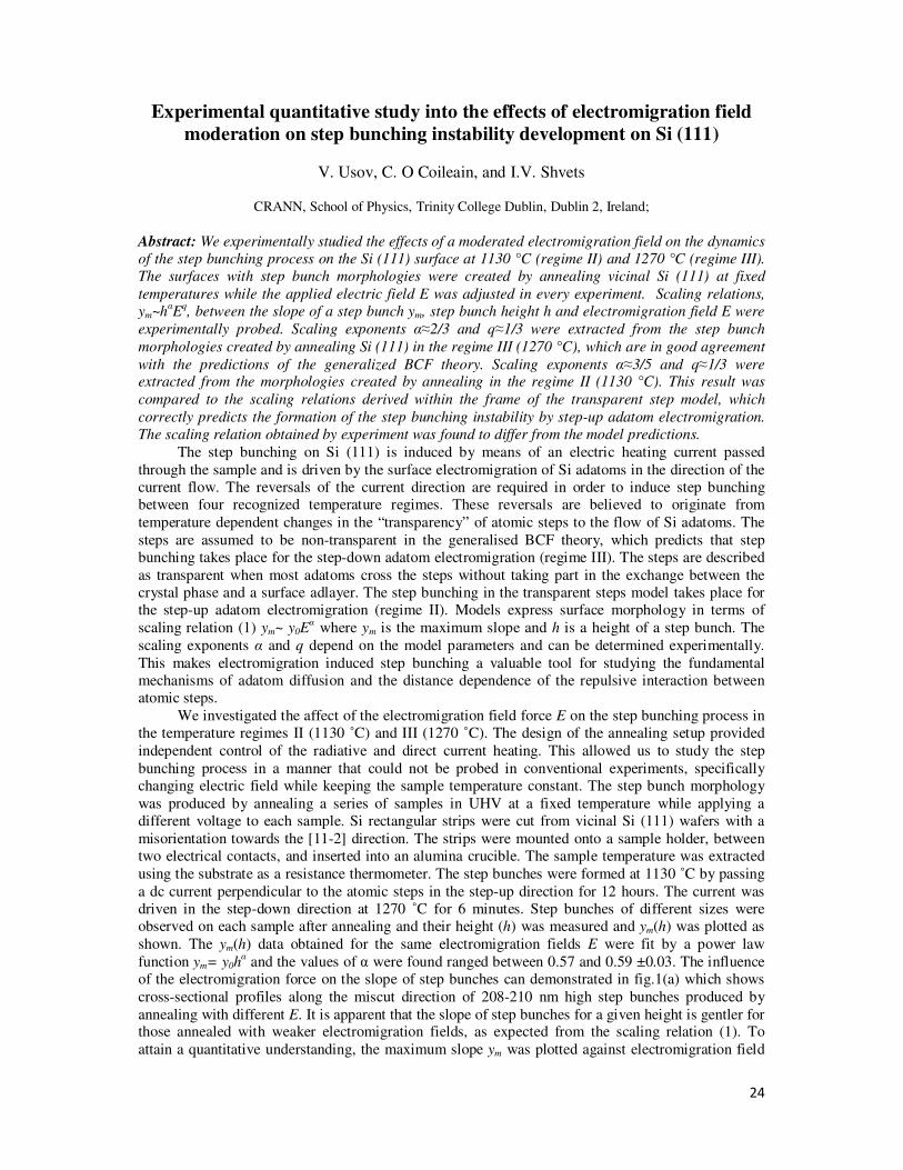
When the applied electric field is reduced below the critical field value (Ecr) the electromigration force is no longer sufficient to initiate the coarsening step bunching process, as is characterised by the gradual growth of step bunches’ heights and terraces’ widths with the annealing time. It should be intuitive, that a repulsive inter-step interaction would necessitate a stronger critical field to induce the step bunching process on surfaces with a reduced initial interstep distance l, which can be determined by the surface’s overall miscut angle (α) from a low index surface. Investigating the Ecr(l) dependency and comparing it to theoretical predictions provides valuable information about the sublimation mechanisms responsible for the development of the step bunching instability on Si (111).
Figure 2 Dependence of critical electric field (Ecr) on the initial average interstep distance (l) at 1130 and 1270 °C (temperature regimes II and III respectively). The annotated angles next to experimental points indicate the corresponding degree of miscut off the Si (111) plane in the [11-2] direction.
For the first time, we were able to study morphologies of step bunched surfaces at the onset stage of antiband formation, created by annealing with moderated E. We were able to test the relationship between the terrace width, electromigration field and the onset of antiband formation predicted by theoretical studies. Also, for the first time we systematically measure values of Ecr for Si (111) with different initial interstep distances l at 1130°C (regime II) and 1270°C (regime III) and compare measured Ecr(l) dependences to the predictions of theoretical models.
This work is published in: C. Ó Coileain, V. Usov, S. Stoyanov, and I.V. Shvets, Critical field
behaviour and antiband instability under controlled surface electromigration on Si (111), Phys. Rev. B. 84, 075318 (2011)

28
6.2.2 Planar Nanowire Arrays (ATLAS)
Magnetic properties of planar arrays of Fe-nanowires grown on oxidized
vicinal silicon (111) templates
S.K. Arora1, B. J. O’Dowd1, P.C. McElligot1, P. Thakur,1 N.B. Brookes,1 and I.V. Shvets1
1CRANN and School of Physics, Trinity College Dublin, Dublin 2, Ireland
2European Synchrotron Radiation Facility, BP220, 38043 Grenoble Cedex, France
Abstract: Planar arrays of Fe nanowires (NW) grown on an oxidized self assembled Si template are shown to be ferromagnetic at room temperature with wire width down to 30 nm as revealed by
magnetometery and x-ray magnetic circular dichorism studies. The atomic terrace low angle shadowing (ATLAS) method used to produce these NW arrays allows one to grow planar arrays that
are several nanometres thick as opposed to monolayer thickness attained with step flow and step
decoration methods. These NW arrays possess much smaller width fluctuations along the wire length
owing to the highly periodic nature of the step-bunched templates. Magnetic anisotropy of the NW array is dominated by the shape anisotropy which keeps the magnetization in-plane with easy axis along the length of the wires.
There has been a considerable amount of interest in studying magnetic nanowires (NWs) over the span of the last two decades, due to their application potential in spin electronic devices and interesting fundamental physics issues. For the bottom up approach, template mediated synthesis of NWs is an attractive option, owing to faster throughput. Template based synthesis of magnetic NWs has been used to produce magnetic NW arrays with reasonable control of size distribution in carefully prepared porous alumina templates in which NWs grow along the thickness of the pores. However, there are relatively few reports related to the production of planar NW arrays based on self-assembled templates using step flow, step decoration and reactive deposition epitaxy (RDE) methods. The small thickness achieved using these methods (leading to superparamagnetism) and material selective nature (applicable only for certain NW material and substrate combinations) restricts their scope for future applications. To overcome the obstacles related to the small thickness of NWs in planar arrays, we use shallow angle deposition on step-bunched vicinal surfaces. We show that the ATLAS grown planar NW arrays are ferromagnetic at RT down to 30 nm wire width and show an in-plane uniaxial anisotropy related to the shape of the NWs.
Figure 1 shows the AFM images of planar arrays of Fe-wires (micro- and nano-) grown on oxidized templates of three highly regular step-bunched different periodicities ranging between 3.2 m to 75 nm. Growth of Fe-NWs was carried out at RT by depositing Fe (0.02-0.04 Å/s) onto the oxidized templates at a small angle (0.5-5o) using a multi-pocket e-beam evaporator. Templates were made from vicinal Si templates by performing a dc-current annealing under ultrahigh vacuum (UHV) conditions on n-type doped Si (111) with resistivity 1-10 .cm (miscut of 2.5 or 4 degrees along (11-2)). By selecting appropriate deposition angle and miscut strength, one can control the coverage of the terraces (i.e. wire width) by modifying the extent of shadowing of the deposited Fe flux caused by the step-bunches. Examples of coverage variation ranging from 40-90 % are shown in figure 1.
Figure 1 (a) AFM phase image of a Fe wire array grown at a deposition angle of 1.2o on oxidized Si template (miscut 2.5o) 3.2 µm periodic template with an average wire width of 1 µm. (b) Phase image of a Fe-NW array grown on 1.1 µm periodic oxidized Si template (miscut 2.5o) template at a deposition angle of 1.7o, leading to 80% terrace coverage (400 nm wire width). (c) AFM height image of a Fe-NW array grown on 75 nm periodic oxidized Si template (miscut 4o) template at a deposition angle of 1.9o. Average width of NWs in this case is 30 nm. A height profile corresponding to the dashed line marked on the Fig.(c) is shown in Fig. (d). Labels BT, NW and SB on the Figs. 1a, 1b and 1d denote bare terrace, nanowire and step bunch respectively. Direction of deposition flux is from left to right for all the three samples.
2 µµµµm NW BT
SB
(a)
500 nm
SB BT NW
(b)
100 nm
(c)
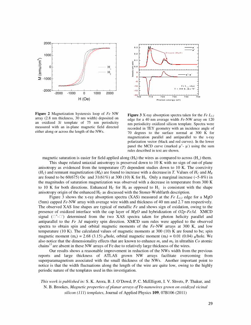
29
Fig.2 shows magnetization hysteresis loops of a
2.8 nm thick MgO capped Fe-NW array with 30 nm average wire width (50% coverage grown on 75 nm periodicity templates at a deposition angle of 1.2o) measured at 300 K with an in-plane magnetic field applied either parallel (H||) or across (H⊥ ) the nanowire length. From magnetization data we infer that the Fe-NW arrays are ferromagnetic at RT. The approach towards
magnetic saturation is easier for field applied along (H||) the wires as compared to across (H⊥) them. This shape related uniaxial anisotropy is preserved down to 10 K with no sign of out-of plane
anisotropy as evidenced from the temperature (T) dependent studies down to 10 K. The coercivity (HC) and remnant magnetization (MR) are found to increase with a decrease in T. Values of HC and MR
are found to be 60(675) Oe and 31(61%) at 300 (10) K for H||. Only a marginal increase (~5-8%) in the magnitudes of saturation magnetization was observed with a decrease in temperature from 300 K to 10 K for both directions. Enhanced HC for H|| as opposed to H⊥ is consistent with the shape anisotropy origin of the enhanced HC as discussed with the Stoner-Wohlfarth description.
Figure 3 shows the x-ray absorption spectra (XAS) measured at the Fe L3,2 edge for a MgO (5nm) capped Fe-NW array with average wire width and thickness of 40 nm and 2.7 nm respectively. The observed XAS line shapes are typical of metallic Fe and shows sign of oxidation, owing to the presence of oxidized interface with the cap layer of MgO and hybridization of O2p-Fe3d. XMCD signal (+--) determined from the two XAS spectra taken for photon helicity parallel and antiparallel to the Fe 3d majority spin direction. XMCD sum rules were applied to the observed spectra to obtain spin and orbital magnetic moments of the Fe-NW arrays at 300 K, and low temperature (10 K). The calculated values of magnetic moments at 300 (10) K are found to be; spin magnetic moment (ms) = 2.68 (3.15) B/hole, orbital magnetic moment (ml) = 0.01 (0.04) B/hole. We also notice that the dimensionality effects that are known to enhance ms and mL in ultrathin Co atomic chains13 are absent in these NW arrays of Fe due to relatively large thickness of the wires.
Our results shows a reasonable improvement in reduction of the NWs width from the previous reports and large thickness of ATLAS grown NW arrays facilitate overcoming from superparamagnetism associated with the small thickness of the NWs. Another important point to notice is that the width fluctuations along the length of the wire are quite low, owing to the highly periodic nature of the templates used in this investigation.
This work is published in: S. K. Arora, B. J. O’Dowd, P. C. McElligott, I. V. Shvets, P. Thakur, and
N. B. Brookes, Magnetic properties of planar arrays of Fe-nanowires grown on oxidized vicinal
silicon (111) templates, Journal of Applied Physics 109, 07B106 (2011)
-2000 -1000 0 1000 2000-2000
-1000
0
1000
2000
M
(em
u/c
m3)
H (Oe)
H⊥
H||
Figure 2 Magnetization hysteresis loop of Fe NW array (2.8 nm thickness, 30 nm width) deposited on an oxidized Si template of 75 nm periodicity measured with an in-plane magnetic field directed either along or across the length of the NWs.
0 .0
0 .1
0 .2
0 .3
7 0 0 7 1 0 7 2 0 7 3 0 7 4 0 7 5 0- 2 0
- 1 5
- 1 0
- 5
0
5
In
ten
sity
(a
rb. u
nit
s)
O x y g e n ( M g O )
F e L3 ,2
e d g e
µµµµ−
µµµµ++++
T = 3 0 0 K , θ = θ = θ = θ = 7 0o
µµµµ++++
− µ− µ− µ− µ−−−−
P h o t o n e n e r g y ( e V )
Figure 3 X-ray absorption spectra taken for the Fe L3,2 edge for a 40 nm average width Fe-NW array on 120 nm periodicity oxidized silicon template. Spectra were recorded in TEY geometry with an incidence angle of 70 degrees to the surface normal at 300 K for magnetization parallel and antiparallel to the x-ray polarization vector (black and red curves). In the lower panel the MCD curve (marked µ+- µ-) using the sum rules described in text are shown.

30
6.2.3 Thin Films
Interplay of bulk and interface effects in the electric-field-driven transition
in magnetite
A. A. Fursina1, R. G. S. Sofin2, I. V. Shvets2, and D. Natelson3, 4
1 Department of Chemistry, Rice University, 6100 Main Street, Houston, Texas 77005, USA; 2 CRANN, School of Physics, Trinity College Dublin, Dublin 2, Ireland;
3Department of Physics and Astronomy, Rice University, 6100 Main Street, Houston, Texas 77005, USA 4Department of Electrical and Computer Engineering, Rice University, 6100 Main Street, Houston, Texas
77005, USA
Abstract: Contact effects in devices incorporating strongly correlated electronic materials are comparatively unexplored. We have investigated the electrically driven phase transition in magnetite
(100) thin films by four terminal methods. In the lateral configuration, the channel length is less than 2 µm, and voltage-probe wires ~100 nm in width are directly patterned within the channel. Multi lead
measurements quantitatively separate the contributions of each electrode interface and the magnetite
channel. We demonstrate that on the onset of the transition contact resistances at both source and drain electrodes and the resistance of magnetite channel decrease abruptly. Temperature-dependent electrical measurements below the Verwey temperature indicate thermally activated transport over
the charge gap. The behaviour of the magnetite system at a transition point is consistent with a theoretically predicted transition mechanism of charge gap closure by electric field.
The complex iron oxide, magnetite, Fe3O4, is an example of strongly correlated 3d-electron systems. It has been known for decades that bulk magnetite undergoes a first order metal-insulator transition (2 order-of-magnitude change in electrical resistivity) at the so-called Verwey temperature, TV ~120 K, accompanied by a structural transformation. Efforts on magnetite characterization are numerous in the last 70 years since the discovery of the Verwey transition, including thorough investigations of its electrical properties supported by theoretical calculations of electronic structure. Recent advances in nanofabrication and film growth allow electrical characterization at previously inaccessible scales, leading to the recent discovery of an electric-field-driven transition: Magnetite films or nanoparticles below TV experience a transition from an insulating state to a state with much lower resistance upon the application of a sufficiently high voltage. The switching voltage scales linearly with the channel length suggesting an electric field-driven transition. The key point of these experiments was an examination of magnetite films or nanoparticles between two electrodes separated by only several hundreds of nanometres or less. In this configuration the electric field needed to drive the transition was accessible at relatively low voltages, thus preventing both excessive heating and damaging of the sample. We proved the observed switching not to be an artefact of heating, in contrast to previously observed transitions in magnetite driven by Joule heating of the samples above TV under bias. The downside of such small channel length experiments is an unavoidable, dominant contribution of the contacts, which prevents direct insight into the properties of magnetite before and after transition. By fitting our data for two-terminal devices with different channel lengths, it was demonstrated that contact resistance of Au/magnetite interfaces comprises more than 70% of the total resistance. Upon testing several different contact metals (Au, Pt, Cu, Fe, and Al), copper showed the lowest contact resistance with magnetite film. Even with a Cu contacting layer, however, the contribution of the contacts to the total two-terminal device resistance cannot be neglected. One of the most effective ways to differentiate between bulk and interface effects is to make multi lead measurements. To date no such experiments have been performed to study the recently discovered electrically driven transition in magnetite. In this work we perform four-terminal experiments in a lateral electrode configuration using magnetite thin films. The channel length is less than 2 µm and voltage probe wires ~100 nm in width are directly inserted into the channel. These multi lead experiments quantitatively and unambiguously separate the role of each interface and the magnetite channel. We studied the changes in contact and channel resistance contributions at the onset of the electric-field driven transition in magnetite.

31
Fe3O4 thin films with 50-100 nm thickness were grown on (100) MgO substrates by oxygen plasma-assisted molecular-beam epitaxy. The films were characterized by high-resolution-XRD, and resistance measurement to prove crystalline quality and stoichiometry of the samples. The films show a jump in the temperature dependence of resistance at Tv ~108 K, characteristic of the Verwey transition in magnetite thin films (fig. 1 (d)). Electrical characterization of the samples was performed by a standard four-terminal method using a semiconductor parameter analyzer. Devices for four-terminal measurements were prepared by electron-beam lithography (fig. 1 (a)).
Figure 1 (a) SEM image of the device for four probe measurements showing source and drain leads and two pairs of voltage probes within the channel. (b) Coloured SEM image demonstrating electrical contacts to micron-sized Au pads with further indium (In) soldering to attach Au wires. (c) Schematics of electrical circuit of four-probe measurements. Letters S and D denote source and drain contact, respectively. Contacts are made of 6 nm Cu adhesion layer (reddish, below) and 10–20 nm cover layer of Au (yellow, above). (d) Temperature dependence of the low-bias resistance of magnetite channel (RDEV) and corresponding contact resistances (RC) at source and drain electrodes. (e) Schematic diagram of voltage distribution along the channel at a transition point (blue open squares) and right after transition (red closed squares). VC denotes the voltage drop at the interfaces.
By doing four-terminal experiments at magnetite thin films below TV we quantitatively separate the contributions of each electrode and the magnetite channel before and after the electric-field-driven transition. For devices of increasing channel lengths we demonstrate the increase in total resistance to be caused by increased contribution of the magnetite channel while contact resistances are unchanged for all channel lengths within 1–2 µm range. At all temperatures the transition is observed (T<TV), contact resistances of both source and drain electrodes and the resistance of magnetite channel decrease abruptly at the transition point. This behaviour is consistent with the mechanism of charge gap closure by electric field predicted in theory.
By doing temperature-dependent electrical measurements below TV we trace the thermally activated transport over the charge gap in magnetite and provide an insight into the transition mechanism in this system. To further explore the field-driven switching mechanism in magnetite, the effect of contact metals with different work functions is currently under study. In the framework of the charge gap closure mechanism, the magnitude of contact resistance jumps at a transition point, RC jump, are expected to be dependent on the work function of the contact metal according to the relative alignment of metal Fermi level and effective Fermi level of magnetite.
This work is published in: A. A. Fursina, R.G.S. Sofin, I.V. Shvets and D. Natelson, Origin of
hysteresis in resistive switching in magnetite is Joule heating. Phys. Rev. B 81, (2010) 045123

32
Probing One Antiferromagnetic Antiphase Boundary and Single Magnetite
Domain Using Nanogap Contacts
Han-Chun Wu, 1 Mohamed Abid, 1, 2 Byong S. Chun,1 Rafael Ramos,1 Oleg N. Mryasov,3 and Igor V. Shvets1
1CRANN, School of Physics, Trinity College Dublin, Dublin 2, Ireland, 2King Abdullah Institute for Nanotechnology, College of Science King Saud University, Riyadh 11451, Saudi
Arabia 3Department of Physics and MINT, University of Alabama, Tuscaloosa, Alabama 35487
Abstract: We have probed one antiferromagnetic (AF) antiphase boundary (APB) and a single Fe3O4 domain using nanogap contacts. Our experiments directly demonstrate that, in the case of probing one AF-APB, a large magnetoresistance (MR), high resistivity, and a high saturation field is observed
as compared with the case of probing a single Fe3O4 domain. The shape of the temperature-dependent
MR curves is also found to differ between the single domain and one of the AF-APB measurements, with characteristic strong temperature dependence for the single domain and temperature
independence for the one AF-APB case. We argue that these observations are indicative of profound changes in the electronic transport across APBs. The investigated APB defects increase the activation
energy and disturb the long-range charge ordering of mono-domain Fe3O4. Epitaxial Fe3O4 films and chemical synthesis nanowires
grown on MgO substrates are reported
to contain anti-phase boundaries (APBs). Due to a modified cationic configuration at the APBs, the nature of magnetic exchange interactions is altered. The presence of these APBs defects leads to the unusual magnetic properties of Fe3O4. Here, based on electron beam lithography (EBL) technology, we have demonstrated the feasibility of probing 1-2 APBs and a single magnetic domain of Fe3O4 using contacts with a nanoscale gap. These experiments show that, in the case of probing APBs, a large MR, high resistivity, and a high saturation field is observed compared to the case of single Fe3O4 domain. Our temperature dependent measurements further show that the shape of MR curves for a single Fe3O4 domain strongly depends on the temperature region. Furthermore, our experiments directly show that the APB increases the activation energy and disturbs the long-range charge ordering of Fe3O4.
It is known that the domain size in magnetite film is dependent on the film thickness. For a 60 nm thick Fe3O4 film, the average domain size is around 50 nm and the thickness of APB is around 2-3 nm. In order to make sure we measure at least one but fewer than 3 APBs, the gap of the contacts should be between 50 to 100 nm (fig. 1 (a)). To probe a single magnetite domain, a pair of contacts with a gap less than 50 nm is necessary (fig. 1 (b)). The lateral geometry of the devices is shown in fig. 1 (d) with a gap of 30 nm. All microstructures discussed in this paper were Fe3O4 epitaxial thin films with thickness of 60 nm. Thin films of Fe3O4 were grown on (001) oriented MgO single crystal substrates using an oxygen plasma assisted molecular beam epitaxy (MBE) system with a base
pressure of 2×10⁻¹⁰
Torr. Device fabrication was carried out by EBL using single layer positive tone resist PMMA supplied by MicroChem Corp. After development, thick metal contacts consisting of Ti (5 nm)/Au (50 nm) were deposited through e-beam evaporation. All these nanogap contacts are along [100] or [010] directions of the films. Subsequently, after lift-off by using acetone, UV lithography was carried out in order to obtain macroscopic metal contacts.
Fig. 1c shows the MR measurements (up to 2 T) for the case of probing 1-2 APBs. The external in-plane field is applied along the current direction. From fig. 1c, one can clearly see that the resistance shows a linear response to the external field which suggest we are measuring one or two AF-APBs. Due to the presence of AF-APBs between the contacts, the electrons encounter a high resistance at the AF-APB. In a field of 2 T, WAF /HMs ≥5, where H is the external field and Ms is the saturation magnetization. For such a strong AF coupling, a magnetic field can align the spins far from the boundary, whereas the spins close to the boundary are only slightly affected by the field. Therefore, the effect of magnetic anisotropy can be neglected and the transport properties of this nano-scaled device are dominated by the transport across the APB, a linear response to the external field is observed which is in a good agreement with our experimental results. A MR ratio of -1.8 %

33
was achieved at room temperature. The MR ratio increases with decreasing temperature and peaks at the TV. Further decreasing the temperature leads to a lowering of the MR ratio. We would like to mention here the shape of the MR curve for this case is independent of temperature.
Figure 1 Schematic of the setup to probe (a) a single APB and (b) a single domain. (d) SEM image of contacts with 30 nm gap. (c) Magneto resistance vs field curve at different temperatures for probing 1-2 APBs. (d) Magneto resistance vs field curve at different temperatures for probing single magnetite domain.
MR measurements for probing a single magnetite domain below TV are shown in fig. 1d. The external in-plane field is applied along the current direction. A small MR ratio of -0.3 % was observed at room temperature which is comparable to the MR ratio of the bulk magnetite.
As can be seen in fig.
1d, nonlinear MR curves were observed for a single domain which is different from the MR curve shapes observed in the case of probing several APBs. As there are no APBs and the gap between the contacts is close to the domain size, the MR effect is due to the rearrangement of spin moments for atoms. When the temperature is above or below TV, at weak fields, the configuration of the spins is only affected by the magnetic anisotropy field. A relatively low field is needed to align the spins far from the boundary, which corresponds to the jump in the MR curve. At strong fields, the spins close to the boundary will start to rotate, a linear behaviour was observed. Around TV, the discontinuous change of the entropy
and the phonon-magnon interaction
play an important role which make the
shape of the MR curve different from those above or below TV and also increase the MR ratio. In summary, we performed the magneto-transport measurements through limited (1-2) numbers
of APBs and single magnetic domain of Fe3O4 thin film. Our experimental results clearly demonstrate that, in the case of probing few APBs, a large MR, high resistivity, and a high saturation field is observed as compared to the case of a single Fe3O4 domain. The former is indicative of the frustrated/perturbed magnetic state in and around APBs, while the MR measurements show how these nano-scale magnetic regions influence the spin dependent scattering. Further we find that the shape of MR curves for single Fe3O4 domain is distinctly temperature dependent while essentially independent for the 1-2 APBs case. Our findings shed light on the origin of spin dependent transport in Fe3O4, and the role of specific defects which are expected to be typical for oxide based nano electronic and spintronic devices.
This work is published in: Han-Chun Wu, Mohamed Abid, Byong S. Chun, Rafael Ramos, Oleg N. Mryasov, and Igor V. Shvets, Probing One Antiferromagnetic Antiphase Boundary and Single
Magnetite Domain Using Nanogap Contacts, Nano Letters 10, 1132 (2010)
APB
Domain
-2 -1 0 1 2
-3
-2
-1
0
APBs
Ti/Au E lectrode
APBs
Ti/Au E lectrode
MR
(%
)
H (T)
40 K
60 K(d)
-2 -1 0 1 2-6
-5
-4
-3
-2
-1
0
1
APB
Ti/Au Electrode
APB
Ti/Au Electrode
MR
(%
)
H (T)
300 K
130 K
110 K
100 K
(c)
(a) (b)

34
Magnetoresistance of Fe3O4-graphene-Fe3O4 Junctions
Zhi-Min Liao,1, 2 Han-Chun Wu,1,3, Jing-Jing Wang,1 Graham L. W. Cross,1,3 Shishir Kumar,1, 4 Igor V. Shvets,1, 3 and Georg S. Duesberg1, 4
1CRANN, Trinity College, Dublin 2, Ireland
2 State Key Laboratory for Mesoscopic Physics, Department of Physics, Peking University, Beijing 100871, P.R. China
3School of Physics, Trinity College, Dublin 2, Ireland 4School of Chemistry, Trinity College, Dublin 2, Ireland
Abstract: The magnetoresistance (MR) of Fe3O4-graphene-Fe3O4 junctions has been experimentally studied at different temperatures. It was found that a barrier exists at the Fe3O4/graphene interface. The existence of the interfacial barrier was further confirmed by the nonlinear I-V characteristics and
non-metallic temperature dependence of the interfacial resistance. Moreover, spin dependent
transport at the interfaces contributes -1.6% MR to the whole device at room temperature and can be regulated by an external electric field.
Graphene is a two-dimensional material with promising applications for spintronics. Here we report on the fabrication and magnetoresistance (MR) properties of Fe3O4-graphene-Fe3O4 junctions. Our experimental results suggest that a barrier exists at the Fe3O4/graphene interface. The spin dependent transport at the interfaces contributes -1.6% MR of the whole devices at room temperature in a dc-two-probe measurement. Furthermore, spin dependent transport at the interfaces was found to be sensitive to the external electric field.
Graphene flakes on a Si substrate with a 300 nm SiO2 layer were obtained by mechanical exfoliation from Kish graphite. The desired graphene flakes were selected under an optical microscope and their positions were recorded by predefined markers on the substrate. Electrode patterns on the graphene flakes were defined by electron-beam lithography. A 50 nm Fe3O4 thin film was grown on the substrate via oxygen plasma assisted molecular beam epitaxy. Finally, Fe3O4-graphene-Fe3O4 junctions were formed after lift-off process. The magneto-transport measurements were performed utilizing a Physical Properties Measurement System (Quantum Design). The inset in fig. 1(a) is a scanning electron microscope (SEM) image of the measured junction device. The upper two Fe3O4 electrodes (contacts 1 and 2 as denoted) contacting the graphene sheet are separated by a distance of approximately 700 nm. The lower two Fe3O4 electrodes (contacts 2 and 3) are connected to each other. The Fe3O4 electrodes are about 2 µm in width and ~ 10 µm in length. The MR of the Fe3O4-graphene-Fe3O4 junction was measured using contact electrodes 1 and 2. However, the resistances of the Fe3O4 electrodes have a significant part in our two-probe devices. To decouple this contribution, the MR of the electrodes was measured using contacts 2 and 3.
The MR, defined as MR=[R(H)-R(0)]/R(0), measured with an in-plane magnetic field are shown in fig. 1(b). We would like to stress the results present here are representative and reproducible. More than three devices have been measured and we got similar results from all the devices.
The MR of Fe3O4-graphene-Fe3O4 junction (red curve in fig. 1(b)) is slightly smaller than that of the Fe3O4 electrodes. The graphene device consists of five distinct regions, two electrodes, two interfaces, and one graphene piece. Therefore, the MR of the device can be formulated as
/
/
2 ( ) ( ) 2 ( )1
2 (0) (0) 2 (0)F G F G
F G F G
R H R H R HMR
R R R
+ += −
+ +, (1)
where RF, RG, and RF/G are the resistances of the Fe3O4 electrodes, graphene, and interface between the Fe3O4 and graphene, respectively. Here, RG may lower the MR of the device as previous studies have indicated a positive MR of graphene at high magnetic fields. Moreover, the interface resistances also contribute to the total resistance. At 300 K, the MR1-2 (-6%) is slightly less than MR2-3 (-6.8%). We would like to stress that, at 300 K, the resistances of the graphene layer and the interfaces amount to approximately a half of the resistance of Fe3O4 electrodes. By subtracting the MR contributing from the Fe3O4 electrodes, one can obtain that the resistance variation from the interfaces and graphene contributes -1.6% MR to the whole junction. Nevertheless, the difference of the MR between the
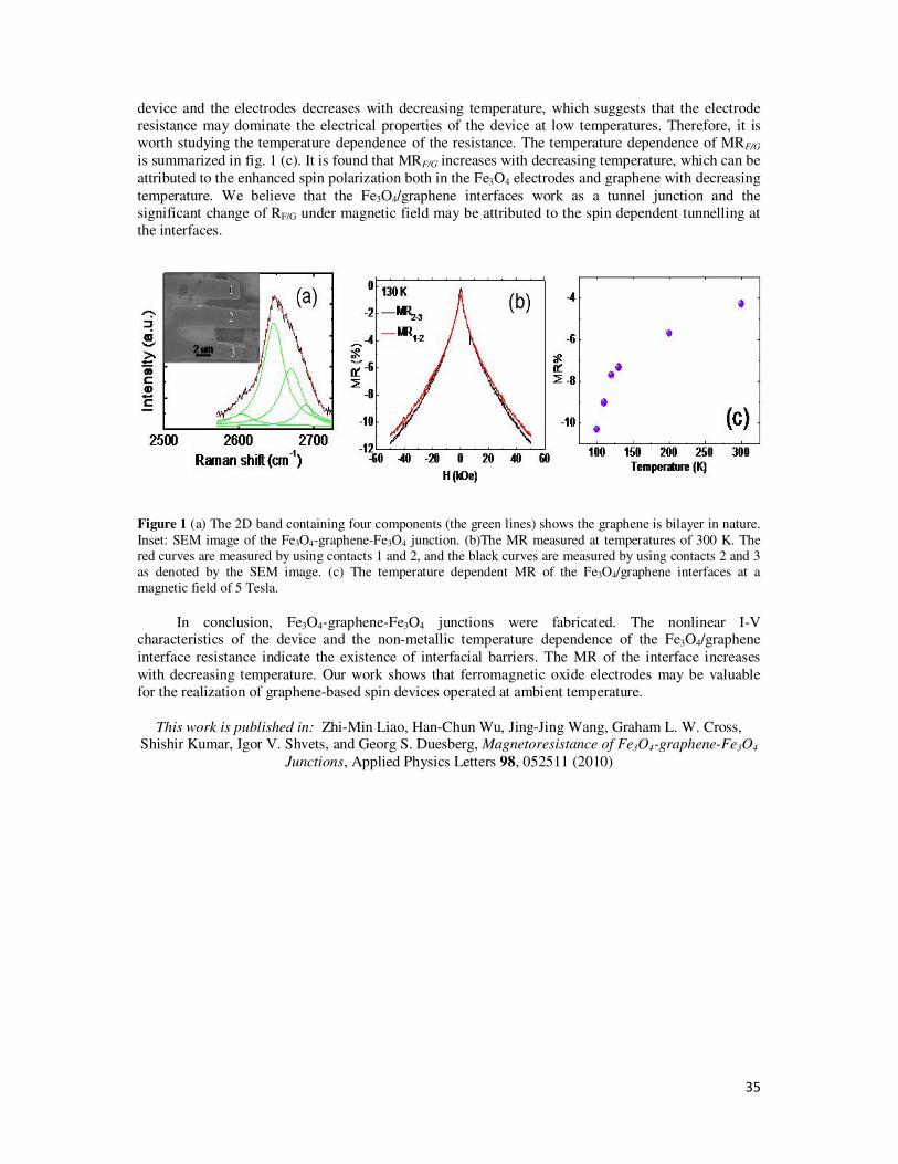
35
device and the electrodes decreases with decreasing temperature, which suggests that the electrode resistance may dominate the electrical properties of the device at low temperatures. Therefore, it is worth studying the temperature dependence of the resistance. The temperature dependence of MRF/G is summarized in fig. 1 (c). It is found that MRF/G increases with decreasing temperature, which can be attributed to the enhanced spin polarization both in the Fe3O4 electrodes and graphene with decreasing temperature. We believe that the Fe3O4/graphene interfaces work as a tunnel junction and the significant change of RF/G under magnetic field may be attributed to the spin dependent tunnelling at the interfaces.
Figure 1 (a) The 2D band containing four components (the green lines) shows the graphene is bilayer in nature. Inset: SEM image of the Fe3O4-graphene-Fe3O4 junction. (b)The MR measured at temperatures of 300 K. The red curves are measured by using contacts 1 and 2, and the black curves are measured by using contacts 2 and 3 as denoted by the SEM image. (c) The temperature dependent MR of the Fe3O4/graphene interfaces at a magnetic field of 5 Tesla.
In conclusion, Fe3O4-graphene-Fe3O4 junctions were fabricated. The nonlinear I-V
characteristics of the device and the non-metallic temperature dependence of the Fe3O4/graphene interface resistance indicate the existence of interfacial barriers. The MR of the interface increases with decreasing temperature. Our work shows that ferromagnetic oxide electrodes may be valuable for the realization of graphene-based spin devices operated at ambient temperature.
This work is published in: Zhi-Min Liao, Han-Chun Wu, Jing-Jing Wang, Graham L. W. Cross, Shishir Kumar, Igor V. Shvets, and Georg S. Duesberg, Magnetoresistance of Fe3O4-graphene-Fe3O4
Junctions, Applied Physics Letters 98, 052511 (2010)

36
Positive APB domain wall magnetoresistance in Fe3O4 (110)
heteroepitaxy films
R.G.S. Sofin, S.K. Arora and I.V. Shvets
CRANN, School of Physics, Trinity College Dublin, Dublin 2, Ireland
Abstract: We observe a strong crystallographic direction dependence on the low field
magnetoresistance (MR) behaviour of epitaxial Fe3O4 (110) films grown on MgO (110) substrates.
The sign of MR is positive when the current and field are parallel to [001] whereas along ]101[
direction its sign is negative similar to that commonly observed for (100) oriented Fe3O4 films. We relate this effect to the presence of antiphase boundaries, APB, and subsequent reduction in the width
of canted spin structure in its vicinity, owing to the hard axis behaviour of Fe3O4 (110) films along
this crystallographic direction. At fields greater than the anisotropy field, usual negative MR behaviour related to a reduction in spin scattering at the APBs is observed. An analytical model
based on the half infinite spin chains across the APBs is provided to show that the positive MR is due
to the domain walls along APBs. The temperature and film thickness dependency of the APB domain
wall magnetoresistance is discussed. The presence of APBs, which are formed due to the difference in the crystal symmetries
between substrate and thin film, leads to a large difference between the physical properties of epitaxial Fe3O4 films and those of the bulk such as larger electrical resistivity, magnetoresistance and magnetization which does not saturate in high magnetic fields. Exchange interactions occurring across some of the APBs must be antiferromagnetic (AF) and experimental evidence suggests that these AF-APBs dominate the magnetic and magnetotransport properties of Fe3O4 thin films. It was shown that
if the spins on neighbouring ions are not parallel, but, instead form an angle nnϕ the transfer integral
is reduced to o nnt t cos / 2= ϕ . Therefore, the transfer of the conduction electrons between ions with
anti-parallel spins at an AF coupled APB is blocked and according to the model the conductivity reduces to zero. The conductivity becomes finite if the angle deviates from π by the application of a magnetic field. This explains the observation of negative magnetoresistance in Fe3O4 thin films grown on MgO substrates. The resistivity contributions from AMR, domain wall magnetoresistance (DWMR), OMR etc are expected to be negligible when compared to the much greater resistivity contribution from AF-APBs in Fe3O4 thin films. In the case of thin films, due to easy plane shape anisotropy, spins far from the APB lie in-plane and at the boundary, the AF coupled spins lie out of plane forming a domain wall across APB which is distinct from the usual 180 degree walls due to the abruptness of the AF coupling at the boundary. Apart from the misalignment of spins in the vicinity of APB due to strongly coupled AF spins across the boundary leading to contribution to MR, the magnetic domain walls formed along the APB (APB-DW) can also contribute to the resistivity. These APB –DW are expected to have widths smaller than conventional ones due to AF exchange at the APB. Thus it could make much greater contribution to DWMR compared to conventional DW. This contribution would be noticeable only at applied field values where, the negative resistivity contribution due to the rotation of AF-coupled spins at the APB is small. Therefore, the density of the APB domain walls is much greater compared to that of conventional magnetic domain walls. In this work, we present the results of MR studies on Fe3O4 (110) films with different thicknesses grown on MgO (110) substrates. A positive longitudinal MR is observed at low fields when current and magnetic field are directed along [001] hard magnetisation axis and a typical negative MR curve is
observed when measured along ]101[ (fig. 1). With an analytical model of half infinite spin chains, we showed that the occurrence of this positive MR at low fields is due to APB-DW (DWMRAPB).
The Fe3O4 thin films were grown using oxygen plasma assisted molecular beam epitaxy, MBE, system (DCA MBE M600) with a base pressure 5x10⁻¹⁰Torr. We have performed detailed studies of structural and magneto transport properties of the films by using High Resolution XRD, Alternating gradient field magnetometer, and low temperature magnetotransport.

37
Figure 1 (1) MR measured at different temperatures for a 90 nm film with in plane field and current directed
along [001] direction. MR measured in ]101[ direction at 300K is also shown;(2) Various spin configurations with applied field (a) field along <-110> direction (b) field along <001> below anisotropy field (c) field along <001> above anisotropy field; (3) The ω-2θ scans for Fe3O4 films with different thickness on MgO (110) substrates; (4) Hysteresis loops obtained for 90 nm Fe3O4 (110) film measured at 300K.
Fe3O4 (110) films show a significant in-plane magnetocrystalline anisotropy which is not
present in Fe3O4 (100) films grown on MgO (100) substrates. We found characteristic differences in
the nature of MR between the longitudinal MR along ]101[ and [001] directions. Longitudinal MR along [001] is positive at fields below the magnetocrystalline anisotropy field. With an analytical model based on the half infinite spin chains across APBs, we have shown that this positive MR at low fields is due to the reduction in the width of the canted spin structure around APBs and associated increase in the spin canting. The anisotropy in the observed MR is due to the difference in the spin configuration at different magnetic field regimes (fig. 1 (2)). This DWMRAPB peaks at a particular temperature Tp and vanishes below Tv. We associate this with the difference between the spin-dependent transport mechanisms and hard-to-easy axis transition across Tv. We have also shown that DWMRAPB depends on the size of the APB domains.
This work is published in: R.G.S. Sofin, S.K. Arora and I.V. Shvets, Positive APB domain wall magnetoresistance in Fe3O4 (110) heteroepitaxy films. Phys. Rev. B 83, (2011) 134436

38
Magneto-transport and Trapping of Magnetic Domain Walls in Spin Valves
with Nanoconstrictions S. J. Noh1, B. S. Chun1, H. C. Wu2, I. V. Shvets2, I. C. Chu3, M. Abid4*, S. Serrano-Guisan5,
and Y. K. Kim1*
1 Department of Materials Science and Engineering, Korea University, Seoul, Korea 2 CRANN, School of Physics, Trinity College Dublin, Dublin 2, Ireland
3 Data & Storage R&D Lab., Seocho R&D Campus, LG Electronics, Seoul, Korea 4 Ecole Polytechnique Federale de Lausanne/IPMC, Station 3, CH 1015, Switzerland
5 Physikalisch-Technische Bundesanstalt, Bundesallee 100, 38116 Braunschweig, Germany Abstract: In a magnetic nanowire, a magnetic domain wall can move along the wire when an external
magnetic field or spin polarized current is applied. The magnetic nanoconstriction systems composed of two wires connected by nano-sized constriction and the presence of a pinned domain wall by
nanoconstriction could be detected via magnetoresistance effects. When the magnetic wire has a
nanometre size constriction, the domain wall configurations and width is largely affected by the nanoconstriction shape. In this study, we investigated the magneto-transport properties and domain
wall pinning and de-pinning in a spin valve structure using nanoconstriction with different shapes.
Our results show an asymmetric magneto-transport curve which is strongly correlated to the shape of the nanoconstriction. These results emphasize the importance of the nanoconstriction shape on the
domain wall instability.
Domain walls (DW) and their motion in magnetic nanowires and stripes have attracted a tremendous amount of attention in fundamental physics and have significant technological potential for devices. The latter has been recently demonstrated for logic and memory devices applications. Here, we investigate the effect of the nanoconstriction shape on DW pinning and de-pinning by using a spin valve (SV) structure in current-in-plane configuration (CIP). Our results show an asymmetric magneto-transport curve which is depends on the applied magnetic field direction with respect to the nanoconstriction shapes.
Samples used for this investigation were of the following stacks; Si/SiO2/Ta nm /NiFe 3 nm /CoFe 5 nm /Cu 2.4 nm /CoFe 3.5 nm /IrMn 10 nm /Ta 5 nm prepared using a six-target dc magnetron sputtering system under the typical base pressure of less than 2 x 10⁻⁷ Torr. Device fabrication was carried out by e-beam lithography using a negative tone ma-N 2403 resist and Ar+ ion etching. Before implementing the nanoconstricted spin valve structure, we fully characterized the exchange coupling strength and the magnetoresistance (MR) of the multilayered spin valve.
Figure 1 (a) Magneto transport properties of the un-patterned Ta 5/NiFe 3.5/CoFe 5/Cu 2.8/CoFe 3.5/IrMn 10/Ta 5 (nm) spin valve sample. (b) A scanning electron microscope (SEM) image of the device. Pads with different sizes are designed, in order to introduce different switching fields by using shape anisotropy. (c) Magneto transport properties of the Ta 5/NiFe 3.5/CoFe 5/Cu 2.8/CoFe 3.5/IrMn 10/Ta 5 (nm) spin valve structure with nanoconstriction.
Fig. 1(a) shows a typical magneto-transport curve of the un-patterned spin valve. This spin valve exhibits a MR of 6% with an exchange coupling strength of 35 mT. This magnetoresistance corresponds to a sensitivity (average slope during the free layer magnetization switching: defined as

39
H
GMRmTS
∆=)/(% ) of 5%/mT in the centre of the ascending branch. Fig. 1(b) shows a scanning
electron microscope (SEM) image of a typical structure we used in this study (top view). In order to trap a domain wall, we have patterned a nanoconstriction into spin valve wire. The V shaped nanoconstriction with a size of 70 nm is located in the middle of two pads with different widths on the top and bottom (reservoirs). These reservoirs are designed to introduce a different switching field due to the shape anisotropy, and act as sources for injecting domain walls into the constriction. The shape anisotropy of the wire constrained the saturation magnetizations of both pinned and free layer to be parallel to wire axis.
Fig. 1(c) shows the magnetotransport of the Ta 5/NiFe 3.5/CoFe 5/Cu 2.8/CoFe 3.5/IrMn 10/Ta 5 (nm) spin valve structure with a nanoconstriction [SV (NC)]. This curve exhibits typical asymmetry behaviour with different peculiarity. When the field is swept from negative to positive and back, first all the layers are aligned parallel to the field direction (lowest resistance state which corresponds to the saturate state). By increasing the field to the positive direction (black curve in fig. 1c), we start to nucleate the DW inside the largest reservoir (5 µm width) until a head-to-head DW is injected into the free layer of the wire from the reservoir. Secondly, at 6 mT, the DW reaches the constriction and is trapped. Here, we notice the relatively large shift in the MR curves in the nanoconstricted spin valve compare to the un-patterned one. This shift is mainly due to two effects, first the magnetostatic coupling between the pinned and free layer or/and secondly to the imperfect saturation of the free layer, where a few magnetic domains may be present in the parts of the sample but are not probed by the MR measurement.
The resistance vs external field curve show many kinks and jumps, which are related to the DW in the free layer pinning and de-pinning at or near the nanoconstriction. In the field of 12 mT, the magnetization of the free layer and pinned layer are completely in an anti-parallel configuration which leads to the highest resistance state. Further increase of the applied field, a head-to-head DW in the pinned layer is injected to and then trapped in the constriction area. When the external field is larger than 30 mT, finally, the magnetization of free layer and pinned layer are completely in a parallel configuration (lowest resistance state). After reaching the positive saturation field, the external field was then swept to negative direction to nucleate a DW inside the relatively smaller reservoir of 1.4 µm width pad until a tail-to-tail DW is injected into the wire from the reservoir. In contrast to the positive swept, when the DW is injected into the wire, there were less intermediate trapping steps at the nanoconstriction observed.
As shown in fig. 1(b), the 1.4 µm width reservoir has a large shape anisotropy compare to 5 µm width, which means that the DW injected from the smaller pad is wider and has less trapping steps which can be understood from the instability of the DW configuration. Therefore, in a constriction between the two pads, a much more complicated pinning process is expected.
In summary, we investigated the magnetic domain wall pinning and de-pinning by using a spin valve structure with a constriction. Our results show an asymmetric magneto-transport curve depending on the applied magnetic field direction with respect to the nanoconstriction shapes. Our results show an asymmetric magneto-transport curve which is strongly correlated to the shape of the nanoconstriction. When the DW injected from a small pad with the small angles between the x axis and the edge of the wire has less intermediate trapping steps at the nanoconstriction are observed compared to the DW injected from a large pad with the large angles between the x axis and the edge of the wire. These result from the shape anisotropy difference between a small and a large pad. These results emphasize the importance of the nanoconstriction shape on the domain wall instability and are useful for developing domain wall based spin devices and other applications.
This work is published in: S. J. Noh, B. S. Chun, H. C. Wu, I. V. Shvets, I. C. Chu, M. Abid, S.
Serrano-Guisan, and Y. K. Kim, Magnetotransport and Trapping of Magnetic Domain Walls in Spin
Valves with Nanoconstrictions, IEEE Transactions on Magnetics 47, 2436 (2011)
40
Memory and Threshold Resistance Switching in Ni/NiO Core-shell
Nanowires
Li He1, Zhi-Min Liao1, Han-Chun Wu2, Xiao-Xue Tian3, Dong-Sheng Xu3, Graham L. W. Cross2, Georg S. Duesberg4, I. V. Shvets2, and Da-Peng Yu1
1State Key Laboratory for Mesoscopic Physics, Department of Physics, Peking University, Beijing 100871, PR
China 2CRANN and School of Physics, Trinity College Dublin, Dublin 2, Ireland
3Institute of Physical Chemistry, State Key Laboratory for Structural Chemistry of Unstable and Stable Species, Peking University, Beijing 100871, PR China
4CRANN and School of Chemistry, Trinity College Dublin, Dublin 2, Ireland Abstract: We report on the first controlled alternation between memory and threshold Resistance Switching (RS) in single Ni/NiO core-shell nanowires by setting the compliance current (ICC) at room
temperature. The memory RS is triggered by a high ICC, while the threshold RS appears by setting a low ICC, and the Reset process is achieved without setting a ICC. In combination with first-principles
calculations, the physical mechanisms for the memory and threshold RS are fully discussed and attributed to the formation of an oxygen vacancy (Vo) chain conductive filament and the electrical
field induced breakdown without forming a conductive filament, respectively. Migration of oxygen
vacancies can be activated by appropriate Joule heating and it is energetically favourable to form conductive chains rather than random distributions due to the Vo-Vo interaction, which results in the non-volatile switching from the off- to the on-state. For the Reset process, large Joule heating
reorders the oxygen vacancies by breaking the Vo-Vo interactions and thus rupturing the conductive filaments, which are responsible for the switching from on- to off-states. This deeper understanding of
the driving mechanisms responsible for the threshold and memory RS provides guidelines for the
scaling, reliability and reproducibility of NiO based non-volatile memory devices.
The resistance switching (RS) phenomenon, in which the resistance can be reversibly switched by an external electrical field, has recently received a great deal of attention. Due to the structural simplicity and high switching speed (~ tens of ns), resistance random access memory (ReRAM) devices have been considered as potential candidates for non-volatile memory. Here we report on the first controllable and reproducible alternation between threshold RS and memory RS in a single Ni/NiO core-shell nanowire at room temperature. In combination with first-principles calculations, we show that the threshold RS is purely due to an electric field effect without forming a conductive filament, while the memory RS and RESET processes (i.e. switching from ON to OFF states) are related to the formation and rupture of oxygen vacancy chain conductive filaments which are due to the presence of the Vo-Vo interaction and the breakdown in the Vo-Vo interaction by Joule heating.
Ni/NiO core-shell nanowires were prepared by electrodepositing Ni in the pores of AAO templates and then oxidizing them in air. Fig. 1(a) shows the sketch of the device fabrication and fig. 1(b) is a high-resolution TEM image of part of the nanowire, which shows the crystalline Ni and amorphous NiO structures. The resistive switching characteristics were measured using a Keithley 4200 Semiconductor Characterization System at room temperature. Fig. 1(c) shows the I-V curves of the NiO/Ni core-shell nanowire. The changes in resistance of the device under different electric fields result from changes in resistance of the NiO layer. At ~ 1 V, the device changed from a HRS to a LRS, which is called the SET process. Control of the type of RS by means of compliance current was clearly demonstrated. The threshold RS is triggered by setting ICC = 10-5 A (corresponding to current density ~ 6.7×10⁻⁵ A/m2, and deposited charges ~ 1.5×10⁻² Cm-3s-1), as shown by the red curve in fig. 1(c). The memory RS is initiated by setting ICC = 10-4 A (~ 6.7×10⁻⁴ A/m2 in current density and ~ 0.15 Cm-3s-1 in deposited charge), as shown by the black curve in fig. 1(c). In memory RS, without setting the ICC, the device can be reset to HRS again (the blue curve in Fig. 1(c)).

41
Figure 1 (a) shows the sketch of the device fabrication and (b) is a high-resolution TEM image of part of the nanowire, and (c) the I-V curves show the resistance switching behaviours of the Ni/NiO core-shell nanowire. The threshold RS, memory RS and the RESET processes were achieved by setting different compliance currents.
On the basis of the theoretical calculations, we proposed a general model to explain our experimental results. Setting the compliance current to a relatively low value, the threshold RS is mainly due to an electric-field-driven transition and no conductive filament is formed during the cycle. The observed small loop (Red curve in fig. 1(c)) is due to the negative temperature coefficient of the Zener effect. By setting the compliance current to an appropriate value which corresponds to the Joule heating plus an electric field is sufficient to drive the oxygen vacancies migration to join in the Vo cluster but not enough to depart from the Vo cluster, a conductive oxygen vacancy filament will be formed. The system will then change from HRS to LRS. Withdrawing the applied electric field cannot change the system from LRS to HRS which corresponds to the memory RS (the black curve in fig. 1(c)). The RESET in our devices is primarily due to large Joule heating as no compliance current is set. In the presence of an extremely high current density (without setting the ICC), which leads to a very high local temperature (thermal energy), the Vo-Vo interactions will be overcome, which results in the rupture of the Vo chain. As long as the conductive filament is destroyed, the current will reduce dramatically and the system is frozen to a state with disordered Vo configuration (the blue curve in fig. 1(c)).
In conclusion, the controllable and reproducible alternation between memory and threshold RS was demonstrated for the first time in a single Ni/NiO core-shell nanowire. The underlying mechanisms of electric field induced threshold RS and Joule heating plus electric field induced conductive filament formation during memory RS are described and well understood. Our findings may provide guidelines for the scaling, reliability and reproducibility of NiO based non-volatile memory devices.
This work is published in: Li He, Zhi-Min Liao, Han-Chun Wu, Xiao-Xue Tian, Dong-Sheng Xu, Graham L. W. Cross, Georg S. Duesberg, I. V. Shvets, and Da-Peng Yu, Memory and Threshold
Resistance Switching in Ni/NiO Core-shell Nanowires, Nano Letters 11, 4601 (2011)
0.0 0.2 0.4 0.6 0.8 1.0 1.210
-8
10-7
10-6
10-5
10-4
Set of Threshold RS
Set of Memory RS
Reset of Memory RS
Cu
rren
t (A
)
Voltage (V)
NiO5 nm
Ni
Au Electrodes
Ni
NiO
0.0 0.2 0.4 0.6 0.8 1.0 1.210
-8
10-7
10-6
10-5
10-4
Set of Threshold RS
Set of Memory RS
Reset of Memory RS
Cu
rren
t (A
)
Voltage (V)
NiO5 nm
Ni
Au Electrodes
Ni
NiO
NiO5 nm
Ni
Au Electrodes
Ni
NiO
(a)
(b)
(c)

42
Anomalous magnetisation reversal process due to proximity effects of
antiphase boundaries
R.G.S. Sofin, Han-Chun Wu and I.V. Shvets
CRANN, School of Physics, Trinity College Dublin, Dublin 2, Ireland
Abstract: Here we report anomalous double switching hysteresis loop and high coercivity (~0.1T) in Fe3O4 (110) thin films. Our analytical model based on spin chains confined within small APBDs
suggests a significant proximity effect of antiferromagnetic APBs. Furthermore, the calculated
domain size (D) follows the well-known scaling relation = √. The results suggest that the interface exchange coupling between neighbouring magnetic domains through antiferromagnetic
APBs is responsible for the double switching hysteresis. Our findings could help advance the studies
of anomalous properties of magnetic materials originating from growth defects. This effect can be utilized for the tunability of exchange bias in devices.
Anomalous magnetic properties of ferromagnets originating due to defect driven structural modifications have received much attention in application oriented research. Antiphase boundaries (APB) are natural growth defects occurring due to the symmetry difference between the thin film and the substrate crystal structures. Studies of epitaxial thin films and hetero-structures containing APBs have attracted considerable attention during the last decade as APBs can significantly alter the physical properties of thin films, which is advantageous for the development of spintronic devices. One of the important epitaxial heterostructures for these studies is Fe3O4 thin films grown on MgO substrates. Since the Fe3O4(Fd3m) crystal structure is lower in symmetry than MgO (Fm3m) there are several equivalent nucleation sites on the MgO surface, which enforce the formation of APBs at the junctions of neighbouring grains. The APBs can be considered as the disruption of cation chains in a continuous oxygen lattice. In Fe3O4/MgO hetero-epitaxy, there exist many new exchange interactions across APBs which are not present in the bulk. The observation of magnetoresistance in Fe3O4 films is explained on the basis of spin polarised conduction across the antiferromagnetically (AF) coupled APBs. Our previous analysis shows that in Fe3O4 (110)/MgO (110) films, APBs can be formed with three different shift vectors, i.e. 1 2 < 001 >⁄ along < 001 > and√3 2 < 111 >⁄ or √3 2 < 111 >⁄ along < 110 > direction. The islands separated by these shift vectors form APBs when they coalesce. Fig.1.a shows one such possible APB formation with the boundary along the h¯ 110i direction. We can identify two important super exchanges across these APBs which are 180o Fe-O-Fe and Fe-O-O-Fe, both AF in nature. It is well known that the size of the domains (D) enclosed by APBs shrinks with a decrease in film thickness (t), following the scaling relationD = C√t . In this work, we report the observation of strong film thickness dependent double switching behaviour in Fe3O4 (110) / MgO (110) films. We demonstrate that the double switching behaviour in these films is a result of disruption of the exchange interaction in proximity to APBs, so that some areas in the film become antiferromagnetically exchange coupled with each other.
The Fe3O4 thin films were grown on (110) oriented MgO single crystal substrates using oxygen plasma assisted molecular beam epitaxy, MBE, system (DCA MBE M600) with a base pressure 5x10-
10 Torr. Structural characterisation of the films was performed using a multi-crystal high-resolution x-ray diffractometer, HRXRD (Bede-D1, Bede, UK). HRXRD results show no other iron oxide phases other than Fe3O4. From previous work we know our Fe3O4 films do not contain any un-reacted Fe clusters or other impurities such as Mg in the bulk or interface of the film. Fig. 1 shows hysteresis loops (HL) obtained at room temperature with magnetic field aligned along [110] (M is normalized with saturation magnetisation, Ms). The HLs show a double switching behaviour with two switching fields Hc1 and Hc2, being strongly thickness dependent, while with field along [001] they show hard axis behaviour. The double switching HL presented here is representative and reproducible. All our (110) films with thickness less than 60 nm showed similar behaviour. Although bulk magnetite has cubic anisotropy with a < 111 > easy axis, reports on magnetisation studies in Fe3O4 (110) epitaxial films grown on MgO (110) substrates, show a square hysteresis loop with an in plane < 110 > easy axis and hard axis along < 001 >, which are broadly consistent with our measurements.

43
Figure 1 (1) Normalized magnetisation loops. Inset shows the possible spin configurations of a small (S) and a large (L) magnetic domains under interfacial exchange coupling. Insets (a) and (c) are the cases above the critical field where the magnetisation in the small domains are pinned to the direction of the field In order to accommodate the AF coupling at the boundary the out-of-plane component of magnetisation has to be in the large domain, which is due to the rotation of spins from anti-parallel to parallel configuration with a small angle between the spins; and (2) Variation of calculated domain size, D with film thickness. The straight line represents a fit to the data using the scaling relation D = C√t.
At a sufficient field all the spins far from the AF APBs follow the direction of H and spins near to the AF-APBs gradually rotate towards 90 degree out-of- plane with respect to the field, in order to facilitate AF coupling across the boundary. Zeeman energy has to compete with anisotropy energy and ferromagnetic exchange energy in order to align the spins towards the field direction. By considering the spin coherent rotation inside the domain, the angle between the spins, θ is inversely proportional to D, the domain size. As D decreases with t, θ increases and a greater field is needed to compensate the anisotropy and exchange energy. Therefore, the critical field increases with decreasing film thickness. In order to estimate the critical field, we consider a model of a spin chain on one side of the AF-APB which is widely used for the analysis of magnetoresistance in Fe3O4 films. In the present case the field is applied along [110] direction and the magneto crystalline anisotropy energy density is also considered. This model is then modified to position a second AF-APB at a certain distance away from the first AF-APB. In this case we can write the energy per unit area of a
chain as: 2
o 2001 o s F
1 d( , H) M H(1 cos ) K cos 2 A dx
4 dx−λ
ϕ γ ϕ = − ϕ + ϕ + ∫
, where φ is the angle
between local saturation magnetisation Ms at distance x from the boundary and field H. λ is the distance from the APB at which the spins are approximately aligned along the field. K is the magneto crystalline anisotropy constant and AF is the exchange stiffness constant. Our analytical model calculates the approximate APB domain size which follows the well known scaling relation (Fig. 1 (2) ). Interfacial exchange coupling between magnetic domains across AF-APBs is also discussed. By changing the density of the APBs using suitable annealing conditions or using stepped substrate surfaces the effect can be tuned for device applications.
This work is published in: R.G.S. Sofin, H. C. Wu and I.V. Shvets, Anomalous magnetisation reversal
process due to proximity effects of antiphase boundaries Phys. Rev. B 84, (2011) 212403

44
6.2.4 Plasmonic Nanoparticles Arrays (ATLAS)
In-Situ Characterization of One-Dimensional Plasmonic
Ag Nanocluster Arrays
R. Verre1, K. Fleischer1, R. G. S. Sofin1, N. McAlinden2, J. F. McGilp2, and I. V. Shvets1, 2
1CRANN, School of Physics, Trinity College Dublin, Dublin 2, Ireland 2School of Physics, Trinity College, Dublin 2, Ireland
Abstract: One-dimensional Ag nanoparticle arrays have been grown on step-bunched vicinal Al2O3
in ultrahigh vacuum using deposition at a glancing angle. The as-grown structures showed a strong optical anisotropy in the visible region of the spectrum. The optical anisotropy was measured in-situ using reflection anisotropy spectroscopy (RAS). The relevant optical properties were determined as a
function of Ag thickness and deposition angle. A simple phenomenological model was developed to
reproduce the features seen in the spectra. With this model it was possible to use the inhomogeneous
broadening as a guide to the nanoparticle dispersion. Metallic NP arrays have proven to be of fundamental importance for optoelectronic
applications and improved solar cells. Such interacting metallic systems have been intensely investigated also as templates for surface enhanced spectroscopy. The required NP arrangements can be readily obtained using lithographic techniques, but these are unsuitable for the production of large scale active areas. Typical colloidal processes could be a solution, but ordered deposition onto a substrate is required. In this study glancing angle deposition is demonstrated to provide a valuable alternative production method. A collimated adatom flux is directed towards a stepped surface, whose steps act as preferential growth sites. Adatoms then diffuse along the steps and coalesce, forming NP arrays. This self-assembled technique is simple, easily scalable and mainly dependent on geometrical considerations. The stepped substrates were produced by annealing in atmosphere at high temperatures from off-cut single crystal c-plane Al2O3 (see fig. 1 a). The chosen substrate was then loaded in an ultra high vacuum environment and exposed to an Ag adatom flux. Due to the anisotropy of the textured template, NP arrays are produced (see fig. 1 b) and possess a strong optical polarization-dependent anisotropy. Reflectance anisotropy spectroscopy (RAS) was demonstrated to be a spectroscopic technique able to quantify these differences and has been used to determine the evolution of the plasmonic properties of the system in-situ during growth (see fig. 1 c). The bare substrate showed a negligible RAS signal, confirming the overall in-plane optical isotropy of c-plane Al2O3. After Ag deposition, all samples showed double peak features due to plasmon resonances. It has been demonstrated that RAS and polarized transmission spectroscopy provide equivalent information. In particular, the positive peak of the RAS reproduces the absorption profile when light is polarized along the array, while the negative peak reproduces the absorption peak for light polarized perpendicular to the array. The peak heights increase with Ag coverage due to increased reflectance of the anisotropic layer and the peak positions undergo a red shift, suggesting that glancing angle
deposition can produce tunable structures.
Figure 1 a) A 2 × 2 µm2 AFM image of a step-bunched c-plane Al2O3 substrate after first-order subtraction. The surface is off-cut 3 along the [1210] direction. After annealing in atmosphere at 1350° C for 24 h, the surface is
c) b) a)

45
covered by uniform, parallel, and straight steps. b) A 1.5 × 1.5 µm2 SEM image and magnified (inset) 300 × 100 nm2 image of the substrate after 4-nm Ag deposition. The sample was loaded in the chamber and inclined at 6° to the Ag atom flux. The surface appears covered by an aligned chain of Ag NPs along the step edge slightly elongated along the chain direction. The measured equivalent radius is 7.9 ± 1.9 nm. c) RAS spectra of the same sample monitored in situ for different nominal thicknesses. After deposition, two broad optical resonances are measured.
The RAS signal observed depends critically on the growth conditions of the Ag NP arrays. A systematic study was undertaken to establish how the RAS changes with substrate morphology and Ag deposition angle. It was demonstrated that the amplitude generally reduces as the deposition angle increases as significant isotropic island formation on the terrace can be seen, which reduces the RAS amplitude. Conversely, at small deposition angles large island shadowing reduces the order that can be obtained and broadens the resonances due to Gaussian dispersion (see fig. 2 a).
Figure 2 a) RAS spectra of the 6deg off-cut sample for different deposition angle. At glancing angles the resonance appear broadedr due to shadowing effect of the islands. Using the one-dimensional model developed a fitting of the curves have been optained. b) A linear relationship between the Γ fitted value and the morphological dispersion σ determined by SEM can be observed, showing a strong correlation between the two.
The Ag NP arrays were also modelled as an infinite one dimensional array of equally spaced metallic NPs of radius R, interacting via coupled dipolar plasmon modes. This is the main excitation mode and each nanodot acts as a point antenna interacting with their neighbours. Using this approach, an expression for the absorption coefficients can be obtained and the RAS spectra reproduced by a simple adaptation of the model to allow for the effect of island anisotropy. The model is able to describe the evolution for different deposited thickness, the presence of the strong RAS signal and allow for the extraction of semi quantitative information on the overall order of the produced system. This is realized with the fitted Γ parameter, which describes the broadening of the positive peak. Fig. 2 b demonstrates that there is a linear relationship between the fitted Γ parameter and the morphological dispersion measured with SEM and extracted by image analysis. This result suggests than that RAS can then not only measure the resonance energy of tunable Ag NP arrays during growth, but it can also monitor the overall order of the surface through the Gaussian broadening of the main peak. RAS has been proved to be a very promising in-situ growth monitoring technique, which can provide not only the resonance peak energies and spectral features for anisotropic arrays of plasmonic NPs, but can also be used as a powerful tool for monitoring their order. In particular, information can be provided reproducibly, reliably, and without the need for microscopy techniques, which are time consuming and can require the exposure of the samples to atmospheric contaminants. This work is published in: R. Verre, K. Fleischer, R. G. S. Sofin, N. McAlinden, J. F. McGilp, and I.
V. Shvets, In situ characterization of one-dimensional plasmonic Ag nanocluster arrays, Physical Review B 83, 125432 (2011)
a) b)

46
Probing the Out-of-Plane Optical Response of Plasmonic Nanostructures
using Spectroscopic Ellipsometry
R. Verre, K. Fleischer, C. Smith, N. McAlinden, J. F. McGilp, and I. V. Shvets
CRANN, School of Physics, Trinity College Dublin, Dublin 2, Ireland
Abstract: A simplified approach to investigate the out-of-plane response of plasmonic nanostructures,
using spectroscopic ellipsometry (SE) is presented. One-dimensional self-assembled arrays of Ag nanoparticles (NPs) were grown on stepped Al2O3 (0001), in ultra-high vacuum, using deposition at a
glancing angle. The SE response was measured with the plane of incidence aligned along, and across, the surface steps. From the raw data an anisotropic surface excess function (ASEF) can be extracted, whose properties depend only on the dielectric function of the NP layer. Three resonances are clearly
seen in the ASEF: two in-plane resonances, which correspond to the resonances, measured using
normal incidence reflection anisotropy spectroscopy, and the out-of-plane resonance. A dipole model
is used to simulate the optical response of the NP layer, where the presence of the out-of-plane resonance provides an important additional constraint in developing the model.
Localised surface plasmon allow tuning of the optical properties of patterned nanoscopic objects within the visible wavelength range, thus opening novel possibilities for optoelectronics, solar cells or biological analysis. The resonant profile of plasmonic nanostructures is usually investigated in the far field with common spectrometers and only the in-plane properties are addressed. Much less effort has been devoted to the characterisation of the out-of-plane LSP resonances in plasmonic materials due to the difficulty of measuring the out-of-plane component with common absorption spectrometer geometries. Spectroscopic ellipsometry (SE) can overcome this limitation but a model is required and the model needs to be compared with the experiment to extract the key optical properties of the investigated material.
Here we report how a quantity, the anisotropic surface excess function (ASEF), can be extracted directly from the measured signal. The great advantage of ASEF is it is dominated by the optical properties of the plasmonic layer only. Thin plasmonic structures with in-plane anisotropy can be measured the only limit to the approach being that the substrate must be optically isotropic.
The usefulness of this approach is demonstrated on a system consisting of Ag NP arrays deposited on stepped c-plane Al2O3 substrates using glancing angle deposition. The textured substrate has been prepared by high temperature annealing in atmosphere and the Ag NPs have been produced by exposing the substrate to the adatom flux at a glancing angle. The typical resulting morphology is shown in fig. 1a. The sample was subsequently measured by SE in two configurations, i.e. with the plane of incidence parallel and perpendicular to the array axis and compared with the bare substrate. For the two measurement configurations, the real part of the pseudo-dielectric function of the whole system is presented in fig. 1 b and three resonances have been attributed to three distinct plasmonic modes, along the NP array (x resonance) perpendicular to the array (y resonance) and out-of-plane (z resonance).
The main complication of the direct analysis of the resulting spectra is due to the presence of the substrate (which complicates the analysis) and by an unusual correspodence with the absorptive response of the NP layer. These two effects have been explained by the introduction of the ASEF using a simple formula. The resulting imaginary part of the ASEF for parallel and perpendicular configuration is shown in fig. 2 A. The great advantage of ASEF is it depends on the properties of the NP layer only with a simple linear relation.
In order to reproduce the signal obtained, a dipolar model was finally used to calculate the effective dielectric function of the NP ensemble. The plasmonic layer was modelled as a collection of identical ellipsoids interacting by dipolar forces and placed in a rectangular lattice on the substrate. Under these assumptions an analytical expression for the effective dielectric function of the NP layer was obtained and the ASEF has been finally simulated with the introduction of a fitting parameter to correctly reproduce the interaction between the ellipsoids (see fig. 2 B). A close resemblance between experiment and theory can be seen, supporting the validity of the formalism developed. The validity

47
of this approach for thin plasmonic structures has been finally discussed and appears of general validity even for such in-plane anisotropic structures, provided the substrate being optically isotropic. The full investigation of plasmonic resonances that SE accesses finally produces additional constraints in the modelling of the structures. Once the out-of-plane resonances are accessed, the parameters governing the out-of-plane optical response cannot be treated as fitting parameters and modelling of the overall optical response is quite severely constrained.
Figure 1: (A) 700 x 700 nm2 SEM image of Ag NP arrays grown at glancing angle of 6° for 20 minutes on a faceted Al2O3 template. The substrate was annealed in air at 1350° C prior to deposition. Ag was subsequently deposited 20 minutes at 6 deposition angle with respect to the average surface orientation with a rate of deposition at normal incidence of 0.2 nm/min. In the inset the AFM image of the substrate prior to deposition can be seen. (B) Real part of the pseudo-dielectric function extracted from the ellipsometry measurements.
Figure 2 (A) Imaginary part of the ASEF. (B) Imaginary part of the simulated ASEF for different scaling factor of the interaction coefficients. The morphological parameters used were extracted from SEM analysis. In the inset, the NP layer effective dielectric function is shown.
This work is published in: R. Verre, K. Fleischer, C. Smith, N. McAlinden, J. F. McGilp, and I. V. Shvets. Probing the out of-plane optical response of plasmonic nanostructures using spectroscopic
ellipsometry, Physical Review B, 84 085440(2011)
B A

48
6.3 Cleaner Energy Laboratory
Magnesium, nitrogen codoped Cr2O3: A p-type transparent conducting oxide
E. Arca1, K.Fleischer1, and I. V. Shvets1
1 CRANN, School of Physics, Trinity College Dublin, Dublin 2, Ireland;
Abstract: A p-type transparent conductive oxide (TCO) was synthesised by co-doping of poorly conducting chromium oxide (Cr2O3) with magnesium and nitrogen. We demonstrated that the co-
doping produced a TCO with good figure of merit despite using spray pyrolysis for deposition. The
nitrogen enhances the specular transparency of the films in the visible range (400-700 nm), and Mg
improves the conductivity while retaining the p-type character of the material. Co-doping with both elements produces a p-type oxide with a low resistivity of 3 X cm and transmission up to 65% for a 150 nm thick film. A comparison with other known p-type materials is given.
p-type transparent conducting oxides (TCOs) have attracted much attention since the deposition of thin films of CuAlO2 delafossite structure was reported in 1997. Producing p-type thin films with both good transparency and high conductivity represents a key challenge in the development of optoelectronics devices such as organic light emitting devices, transparent thin film transistors, and solar cells. Compared to conventional n-type TCOs, p-type oxides are generally less conductive and less transparent, with the lowest resistivity reported to be 0.45 10-2 Ω cm (transmission 30%) and the highest transmission not exciding 70% for oxides.
In this study, a poorly conducting p-type material, chromium oxide (Cr2O3, Eskolaite), was chosen as the host matrix, and both cation and anion doping were performed simultaneously in order to improve the conductivity and enhance the transparency. Spray pyrolysis was used as the deposition technique due to its robustness and versatility, enabling the screening of multiple precursors. For the deposition, Cr(NO3)3 was used as the Cr precursor, deionised water as the solvent, and oxygen as a carrier gas. Doping was carried out using MgCl2·6(H2O) as the cation dopant and NH4CH3CO2 as the anion dopant. Nitrogen incorporation primarily affects the optical properties of the film as measured by UV-Visible spectroscopy. The optical properties of the film do not change upon doping with only Mg, while an increase in transmission has been observed as the nitrogen concentration in the solution was increased (fig. 1).
Figure 1 UV-VIS transmittance of (a) Cr2O3, (b) Cr2O3:Mg, and (c) Cr2O3:(Mg,N) grown with precursor ratios of Cr:Mg 9:1 and Cr:N of 1:4. The inset shows an exemplary SEM cross-section used to determine film thickness.
The origin of the improved transmission cannot be attributed to the presence of a different crystallographic phase or different thicknesses, which were both ruled out by analysing the XRD

49
patterns (fig. 2) and cross sectional SEM pictures (inset fig.1) respectively. Also, the microscopic surface roughness, as determined by AFM, is comparable for all the samples and independent of the nitrogen concentration. There are two more possible reasons for the increased transmittance. Profilometer measurements show the presence of a macroscopic structure in the order of 10-50 m scale caused by the impact of larger, not fully evaporated droplets. Samples grown with nitrogen show less prominent structures, and thus they are more homogeneous. However, this cannot fully explain the higher transmission, especially if one takes into account that a similar increase in transmission has been noted for amorphous Cr2O3 grown by magnetron sputtering in nitrogen rich conditions. This suggests that presence of Cr-N bonds is a contributing factor. All nitrogen only doped samples are poorly conducting or insulating. To increase the conductivity Mg co-doping was performed. Doping with Mg produced a remarkable improvement in the electrical properties while maintaining the p-type character of the current carriers. Mg doping of Cr2O3 alone has previously shown to lead to p-type conductive samples. However, simultaneous (Mg,N) co-doping improves the transmittance of films significantly and at the same time the conductivity is enhanced. This makes this material interesting in the context of p-type transparent conducting oxides for the first time. In order to understand how this material compares with other known p-type TCOs, we calculated the figure of merit in the same way from the published works. The best figure of merit is that of CuCrMgO2 grown by sputtering. However, the same material grown by spray pyrolysis has only a slightly higher figure of merit than Cr2O3:(Mg,N). Furthermore, Cr2O3:(Mg,N) has a higher figure of merit than both the only-Mg doped and only-N doped Cr2O3 reported so far. Cr2O3:(Mg,N) has also a higher figure of merit than many other p-type TCOs reported.
Figure 2 X-ray powder diffraction patterns of (a) undoped, (b) Mg doped, and (c) Mg,N co-doped Cr2O3.
This work is published in: E. Arca, K. Fleischer, and I. V. Shvets, Magnesium, nitrogen codoped Cr2O3: A p-type transparent conducting oxide, Applied Physics Letters, 99 (2011) 111910

50
7. Commercialisation
The Applied Physics Research Group has a very long and productive history of research commercialisation. We have spun out three campus companies since 2000. We dedicate a percentage of our resources to commercialisation and are always looking for the next commercialisation opportunity resulting from our in-house research. The first company, Deerac Fluidics (now acquired by Labcyte Inc, www.labcyte.com ) was spun out in 2000. The company is developing and manufacturing advanced instrumentation for drug development in the pharmaceutical sector. The second company, Cellix Ltd (www.cellixltd.com ) was spun out in 2006 and is manufacturing microfluidics products and technologies for the life science and medical sectors. The company won several national and international awards. The products of Cellix are used by several leading pharmaceutical and biotech companies. The company also made a contribution to science: there is a solid stream of papers in leading international journals from universities and research centres around the worlds utilizing the Cellix microfluidic technology. Both of these companies originated from applied research projects in our group and license the technology from Trinity College.
Cellix VenaFlux platform for automated cell-based assays and drug screening In 2010 we initiated the third company from our research, Miravex Ltd, www.miravex.com . The idea for the company originated from our scanning microwave microscopy project. In 2000-2005 we were developing a scanning microwave microscopy technique and as part of the method we had to measure the 3D topography of an oxide surface by means of optical feedback. We then modified the technical approach employed for the topography measurements and identified an exciting application for it: in the area of aesthetic medicine and diagnostics of dermatological conditions. The technology developed by Miravex is highly sophisticated. The image is collected by illuminating the area from different directions and at different wavelength. In this way one file is composed in a split second combining a matrix composed of dozens of images. Then the computer solves a reciprocal problem composed of a system of dozens of equations to compose a single 3D topographical and spectroscopic image of the surface.
Optical topographic and spectroscopic imaging device from Miravex

51
The company left the Trinity campus in 2011. The first year was very successful for Miravex and the company sold a significant number of instruments in Europe, Asia, North and South Americas, and Middle East. The company won the prestigious ITLG- Irish Technology Leadership Group Award, the Irish- US organisation based in Silicon Valley stimulating Irish high tech and innovative companies and harnessing leadership and vision among Irish entrepreneurs. Like the two earlier companies, Miravex, is lead by former research students from the group. Dr. Guido Mariotto and Dr. Roman Kantor completed their PhDs in the group in the 1990s and remained in the group as research fellows for many years. They bravely decided to leave the comfort of a university lab for the risky world of commercial realities. We wish them success in the current challenging economic climate.
The founders of Miravex, Dr. Roman Kantor, Dr. Guido Mariotto, Prof. Igor Shvets, receive Enterprise Ireland Research Commercialisation Award. The Applied Physics Research group is developing new technologies for commercialisation.

52
8. Group Dissemination
8.1 Peer Review Publications
S. I. Bozhko, S. A. Krasnikov, O. Lübben, B. E. Murphy, K. Radican, V. N. Semenov, H. C. Wu, B. Bulfin, and I. V. Shvets
Rotational transitions in a C60 monolayer on the WO2/W (110) surface
Physical Review B 84 (19), 195412 (2011) Li He, Zhi-Min Liao, Han-Chun Wu, Xiao-Xue Tian, Dong-Sheng Xu, Graham L. W. Cross, Georg S. Duesberg, I. V. Shvets, and Da-Peng Yu
Memory and Threshold Resistance Switching in Ni/NiO Core-Shell Nanowires Nano Letters 11 (11), 4601 (2011)
O. Lübben, S. A. Krasnikov, A. B. Preobrajenski, B. E. Murphy, and I. V. Shvets,
Fe Nanoclusters on the Ge (001) Surface Studied by Scanning Tunnelling Microscopy, Density
Functional Theory Calculations and X-Ray Magnetic Circular Dichroism Nano Research 4 (10), 971 (2011)
S. A. Krasnikov, S. I. Bozhko, K. Radican, O. Lübben, B. E. Murphy, S. R. Vadapoo, H. C. Wu, M. Abid, V. N. Semonov, and I. V. Shvets
Self-Assembly and Ordering of C60 on the WO2/W (110) Surface Nano Research 4 (2), 194 (2011)
V. Usov, C. O Coileain, and I. V. Shvets
Experimental quantitative study into the effects of electromigration field moderation on step
bunching instability development on Si (111)
Physical Review B 83, 155321 (2011) R. G. S. Sofin, S. K. Arora, and I. V. Shvets
Positive antiphase boundary domain wall magnetoresistance in Fe3O4 (110) heteroepitaxial
films Physical Review B 83, 134436, (2011)
R. Verre, K. Fleischer, R. G. S. Sofin, N. McAlinden, J. F. McGilp, and I. V. Shvets
In-situ characterisation of one-dimensional plasmonic Ag nanocluster arrays
Physical Review B 83 (12), 125432 (2011) Coleman JN, Lotya M, O'Neill A, Bergin SD, King PJ, Khan U, Young K, Gaucher A, De S, Smith RJ, Shvets IV, Arora SK, Stanton G, Kim HY, Lee K, Kim GT, Duesberg GS, Hallam T, Boland JJ, Wang JJ, Donegan JF, Grunlan JC, Moriarty G, Shmeliov A, Nicholls RJ, Perkins JM, Grieveson EM, Theuwissen K, McComb DW, Nellist PD, and Nicolosi V
Two-Dimensional Nanosheets Produced by Liquid Exfoliation of Layered Materials
Science 331 (6017), 568 (2011) C. O Coileain, V. Usov, and I. V. Shvets
Critical field behaviour and antiband instability under controlled surface electromigration on Si (111)
Physical Review B 84 (7), 075318 (2011)
S. I. Bozhko, S. A. Krasnikov, O. Lübben, B. E. Murphy, K. Radican, V. N. Semenov, H. C. Wu, B. Bulfin, and I. V. Shvets
Rotational transitions in a C60 monolayer on the WO2/W (110) surface
Physical Review B 84 (19), 195412 (2011)

53
R. G. S. Sofin, H. C. Wu, and I. V. Shvets Anomalous magnetization reversal due to proximity effect of antiphase boundaries Physical Review B 84, 212403 (2011)
O. Lübben, S. A. Krasnikov, A. B. Preobrajenski, B. E. Murphy, and I. V. Shvets
Fe Nanoclusters on the Ge (001) Surface Studied by Scanning Tunnelling Microscopy, Density Functional Theory Calculations and X-Ray Magnetic Circular Dichroism Nano Research 4 (10), p971 (2011)
R. Verre, K. Fleischer, C. Smith, N. McAlinden, J. F. McGilp, and I. V. Shvets
Probing the out-of-plane optical response of plasmonic nanostructures using spectroscopic
ellipsometry Physical Review B 84, 085440 (2011)
Z. M. Liao, H. C. Wu, J. J. Wang, G. L. W. Cross, S. Kumar, I. V. Shvets, and G. Duesberg
Magnetoresistance of Fe3O4-graphene-Fe3O4 junctions Applied Physics Letters 98 (5), 052511 (2011)
S. J. Noh, B. S. Chun, H. C. Wu, I. V. Shvets, I. C. Chu, M. Abid, S. Serrano-Guisan, and Y. K. Kim
Magnetotransport and Trapping of Magnetic Domain Walls in Spin Valves with Nanoconstrictions
IEEE Transactions on Magnetics 47 (10), 2436 (2011)
P. Thakur, R. Kumar, J. C. Cezar, N. B. Brookes, A. Sharma, S. K. Arora, S. Gautam, A. Kumar, K. H. Chae, and I. V. Shvets
Evolution of magnetic nanophases of Ni embedded in Al2O3 (001) matrix by X-ray magnetic circular dichroism
Chemical Physics Letters 501 (4-6), 404 (2011)
S. Serrano-Guisan, H. C. Wu, C. Boothman, M .Abid, B. S. Chun, I. V. Shvets, and H. W. Schumacher
Thickness dependence of the effective damping in epitaxial Fe3O4/MgO thin films Journal of Applied Physics 109 (1), 013907 (2011)
N. E. Rajeevan, R. Kumar, D. K. Shukla, R. J. Choudhary, P. Thakur, A. K. Singh, S. Patnaik, S. K. Arora, I. V. Shvets, and P. P. Pradyumnan
Magnetoelectric behaviour of ferrimagnetic Bi(x)Co(2-x)MnO(4) (x=0, 0.1 and 0.3) thin films
Journal of Magnetism and Magnetic Materials 323 (13), 1760 (2011)
H. C. Wu, M. Abid, B. S. Chun, R. Ramos, O. N. Mryasov, and I. V. Shvets Probing one antiferromagnetic antiphase boundary and single magnetite domain using
nanogap contacts
Nano Letters 10 (4), 1132 (2010) Fursina, R. G. S. Sofin, I. V. Shvets, and D. Natelson
Interplay of bulk and interface effects in the electric-field-driven transition in magnetite Physical Review B 81 (4), 045123 (2010)
S. Chun, H. C. Wu, M. Abid, I. C. Chu, S. Serrano-Guisan, I. V. Shvets, and D. S. Choi
The effect of deposition power on the electrical properties of Al-doped zinc oxide thin films Applied Physics Letters 97 (8), 082109 (2010)
S. A. Krasnikov, S. Murphy, N. Berdunov, A. P. McCoy, K. Radican, and I. V. Shvets
Self-limited growth of triangular PtO2 nanoclusters on the Pt (111) surface Nanotechnology 21 (33), 335301 (2010)

54
M. Belesi, I. Rousochatzakis, H. C. Wu, H. Berger, I. V. Shvets, F. Mila, and J. P. Ansermet Ferrimagnetism of the magnetoelectric compound Cu2OSeO3 probed by Se-77 NMR Physical Review B 82 (9), 094422 (2010)
V. Usov, C. O. Coileain, and I. V. Shvets
Influence of electromigration field on the step bunching process on Si (111) Physical Review B 82 (15), 153301 (2010)
N. Chaika, S. S. Nazin, V. N. Semenov, S. I. Bozhko, O. Lübben, S. A. Krasnikov, K. Radican and I. V. Shvets
Selecting the tip electron orbital for scanning tunnelling microscopy imaging with sub-
ångström lateral resolution EPL (Europhysics Letters) 92 (4), 46003 (2010)
A. Fursina, R. G. S. Sofin, I. V. Shvets, and D. Natelson
Interfacial transport properties between a strongly correlated transition metal oxide and a metal: Contact resistance in Fe3O4/M (M=Cu, Au, Pt) nanostructures
Physical Review B 82 (24), 245112 (2010) J. M. Caicedo, S. K. Arora, R. Ramos, and I. V. Shvets, J. Fontcuberta, and G. Herranz
Large magnetorefractive effect in magnetite
New Journal of Physics 12, 103023 (2010) K. Radican, S. I. Bozhko, S. R. Vadapoo, S. Ulucan, H. C. Wu, A. McCoy, and I. V. Shvets
Oxidation of W (110) studied by LEED and STM Surface Science 604 (19-20), 1548 (2010)
F. Cuccureddu, S. Murphy, I. V. Shvets, M. Porcu, H. W. Zandbergen, N. S. Sidorov, and S. I. Bozhko
Surface morphology of c-plane sapphire (alpha-alumina) produced by high temperature anneal
Surface Science 604 (15-16), 1294 (2010) V. O. Golub, V. V. Dzyublyuk, A. I. Tovstolytkin, S. K. Arora R. Ramos, R. G. S. Sofin, and I. V. Shvets
Influence of miscut direction on magnetic anisotropy of magnetite films grown on vicinal MgO
(100) Journal of Applied Physics 107 (9), 09B108 (2010)
8.2 Conference Oral Presentations
S.R. Vadapoo, S.I. Bozhko, K. Radican, S.A. Krasnikov, O. Lübben, I.V. Shvets Self-assembly of C60 on the oxidized W (110) surface studied by STM and LEED
27th European Conf. on Surface Science (ECOSS27), Groningen, Netherlands, August 29 – September 3, 2010
S.I. Bozhko, V.N. Semenov, K. Radican, O. Lübben, S.A. Krasnikov, S.R. Vadapoo, H.C. Wu, I.V. Shvets
Dynamics of C60 molecule rotation in proximity to ordering transition
18th International Vacuum Congress (IVC18), Beijing, China, August 23–27, 2010 R. Verre, K. Fleischer, R. G. S. Sofin, N. McAlindle, J. McGilp, I. V. Shvets:
In-situ characterisation of tunable Ag nanoparticles arrays grown by glance angle deposition
MRS Spring Meeting, San Francisco, USA, April 2011

55
O. Lübben, S.A. Krasnikov, A.B. Preobrajenski, B.E. Murphy, I.V. Shvets Fe nanocluster arrays self-assembled on surfaces with a preformed row pattern 28th European Conf. on Surface Science (ECOSS28), Wroclaw, Poland, August 28 – September 2, 2011
R. Verre, K. Fleischer, I. V. Shvets:
Highly ordered self-organised plasmonic scatterers E-MRS Spring Meeting, Nice, France, May 2011
Sunil K. Arora, Brendan J. O'Dowd, Paul C. McElligott, P. Thakur, N. Brookes, B. Ballesteros, Pietro Gambardella, Igor V. Shvets:
Structural and Magnetic Properties of Planar Nanowire Arrays of Fe Grown on Oxidised Vicinal Silicon (111) Templates MRS Fall Meeting 2011, Boston, USA, Nov-Dec 2011
E. Arca, K. Fleischer, I. V. Shvets:
An improved p-type TCO and a method to improve transparency and conductivity in
transitional metal oxides
E-MRS Fall Meeting 2011, Warsaw, Poland, September 2011 K. Fleischer, E. Arca, I. V. Shvets:
Band gap tuned ZnO:Al by magnesium inclusion E-MRS Fall Meeting 2011, Warsaw, September Poland, 2011
H. C. Wu:
Charge-Orbital Ordering Driving Phase Transitions in Spin Valves BIT 1st Annual Nano S&T, Dalian, China, November 2011
Z. Liao, H. C. Wu, I. V. Shvets:
Spin dependent transport at Fe3O4/graphene interface
56th Annual Conference on Magnetism and Magnetic Materials, Scottsdale, Arizona, USA, Oct – Nov 2011
S. R. G. Sofin, H. C. Wu, I. V. Shvets:
Proximity effects of antiphase boundaries
56th Annual Conference on Magnetism and Magnetic Materials, Scottsdale, Arizona, USA, Oct – Nov 2011
S.K. Arora, B. J. O'Dowd, C. Nestor, T. Balashov, A. L. Rizzini, J. J. Kavich, S. S. Dhesi, B. Ballesteros, P. Gambardella, I. V. Shvets:
Structural and Magnetic Properties of Planar Nanowire Arrays of Fe Grown on Oxidised
Vicinal Silicon (111) Templates
56th Annual Conference on Magnetism and Magnetic Materials, Scottsdale, Arizona, USA, Oct – Nov 2011
O. Lübben, S. A. Krasnikov, A. B. Preobrajenski, B. E. Murphy, I. V. Shvets:
Self-assembly of Fe nanocluster arrays on templated surfaces 56th Annual Conference on Magnetism and Magnetic Materials, Scottsdale, Arizona, USA, Oct – Nov 2011

56
8.3 Conference Poster Presentations
V. Usov, C. O Coileain, I. V. Shvets: Experimental quantitative study of electromigration field effects on the step bunching instability
on Si (111)
MSM XVII - Microscopy of Semiconducting Materials 2011, Churchill College, Cambridge, UK, April 2011
R. Verre, K. Fleischer, R. G. S. Sofin, N. McAlindle, J. McGilp, I. V. Shvets:
Self-assembled nanoparticle arrays grown at glancing angle: structures with tunable plasmonic
properties
ISSC-18: 18th Interdisciplinary Surface Science Conference, University of Warwick, UK, April 2011
R. G. S. Sofin, H. C. Wu, I. V. Shvets:
Spin frustration due to proximity effects of antiphase boundaries ISSC-18: 18th Interdisciplinary Surface Science Conference, University of Warwick, UK, April 2011
E. Arca, K. Fleischer, I. V. Shvets: An alternative fluorine precursor for the synthesis of SnO2:F by spray pyrolysis
ISSC-18: 18th Interdisciplinary Surface Science Conference, University of Warwick, UK, April 2011
S. K. Arora, B. J. O'Dowd, P. C. McElligott, P. Thakur, N. B. Brookes, B. Ballesteros, P. Gambardella, I. V. Shvets:
Structural and magnetic properties of planar arrays of Fe-nanowires grown using atomic terrace low angle shadowing
ISSC-18: 18th Interdisciplinary Surface Science Conference, University of Warwick, UK, April 2011
V. Usov, C. O Coileain, I. V. Shvets: Influence of electromigration field on the step bunching process on Si (111) surface
ISSC-18: 18th Interdisciplinary Surface Science Conference, University of Warwick, UK, April 2011
S.A. Krasnikov, S.I. Bozhko, K. Radican, O. Lübben, B.E. Murphy, V.N. Semenov, H. C. Wu, I.V. Shvets
C60 monolayer on the tungsten oxide surface: from simple self-assembly to C60 quantum states 18th Interdisciplinary Surface Science Conf. (ISSC-18), Warwick, UK, April 4–7, 2011
E. Arca, K. Fleischer, I. V. Shvets: Alternative precursors for the synthesis of SnO2:F by spray pyrolysis
E-MRS Spring Meeting, Nice, France, May 2011 B. Bulfin, I. V. Shvets: Oxides for thermochemical water-splitting
E-MRS Spring Meeting, Nice, France, May 2011
E. Arca, K. Fleischer, I. V. Shvets: Pole of precursor on optical and electrical properties of ZnO:Al E-MRS Spring Meeting, Nice, France, May 2011
E. Arca, K. Fleischer, I. v. Shvets: Band gap tuned ZnO:Al by magnesium inclusion
E-MRS Spring Meeting, Nice, France, May 2011

57
E. Arca, K. Fleischer, I. V. Shvets: An improved p-type TCO and a method to improve transparency and conductivity in transitional metal oxides
E-MRS Spring Meeting, Nice, France, May 2011
B.E. Murphy, S.A. Krasnikov, S.I. Bozhko, K. Radican, O. Lübben, V.N. Semenov, H.-C. Wu, I.V. Shvets
C60 monolayer on the tungsten oxide surface: from simple self-assembly to C60 quantum states
35th Annual Symposium of Microscopy Society of Ireland (MSI2011), Dublin, Ireland, August 24-26, 2011
E. Arca, K. Fleischer, I. V. Shvets:
Role of precursors on optical and electrical properties of ZnO:Al E-MRS Fall Meeting 2011, Warsaw, Poland, 2011
R. Verre, K. Fleischer, J. F. McGilp, I. V. Shvets:
Self-assembled nanoparticle arrays grown at glancing angle: strcutures with tunable plasmonic
properties
Photonics Ireland, Dublin, Ireland, 2011 E. Arca, K. Fleischer, I. V. Shvets:
Role of precursors on optical and electrical properties of ZnO:Al 26th European Photovoltaic Solar Energy Conference, 26th European Photovoltaic Solar Energy Conference, 2011
K. Fleischer, E. Arca, I. V. Shvets:
Band gap tuned ZnO:Al by magnesium inclusion
26th European Photovoltaic Solar Energy Conference, 26th European Photovoltaic Solar Energy Conference, 2011
R. Verre, K. Fleischer, I. V. Shvets:
Highly ordered self-organised plasmonic scatterers 26th European Photovoltaic Solar Energy Conference, 26th European Photovoltaic Solar Energy Conference, 2011
H. C. Wu, O. N. Mryasov, I. V. Shvets:
Temperature-dependent tunnelling interlayer exchange coupling in epitaxial (001)
NiO|Fe3O4|MgO|Fe3O4 exchange biased nano-structures 56th Annual Conference on Magnetism and Magnetic Materials, Scottsdale, Arizona, USA, Oct – Nov 2011
S. K Arora, B. J. O'Dowd, I. V. Shvets: Magnetic behaviour of Fe0.2Ni0.8 films coupled to planar nanowire arrays of Fe 56th Annual Conference on Magnetism and Magnetic Materials, Scottsdale, Arizona, USA, Oct – Nov 2011

58
8.4 Awards
R. Verre, K. Fleischer, O. Ualibek, I. V. Shvets – Best Poster Award @ Photonics Ireland, Dublin, Ireland, 2011
Self-assembled nanoparticle arrays grown at glancing angle: structures with tunable plasmonic
properties
Miravex - G. Mariotto, R. Kantor, I. V. Shvets First Eircom University Challenge Award @ Irish Technology Leadership Group Forum November 2010

59
9. Research Students Graduated
9.1 PhD
Rafael Ramos Anisotropic magneto-transport properties of epitaxial magnetite thin films
February 2010 Ruggero Verre
Spectroscopic studies of self-assembled plasmonic nanoparticle arrays
September 2011 Cormac Ó Coileain
Controlled electromigration on vicinal surfaces November 2011
9.2 MSc
Sundar Raja Vadapoo Self-assembly of C60 molecules on oxidised W (110) surface
September 2010 Paul McElligott
Formation of Magnetic Nanowires on Step Bunched Self Assembled Silicon (111) and Silicon Dioxide Templates
January 2011