trm-915-dts / trm-915-dts-brz data guide - mouser electronics 5-30... · controller to form a...
TRANSCRIPT
TRM-915-DTS / TRM-915-DTS-BRZ
Data Guide(Preliminary)
Table of Contents1 Introduction2 Features
2 Applications
2 Electrical Specifications2 Absolute Maximum Ratings
4 Detailed Electrical Specifications
7 Module Overview7 Theory of Operation7 General
12 Operating States
13 Resetting Module to Factory Defaults
13 Hardware Reset
14 Application Information14 Pin-out Diagram
14 Pin Description
15 Mechanical Drawings
16 Example Circuit
17 Power Supply
18 UART Interface
18 Antenna
19 Link Budget, Transmit Power and Range Performance
21 Module Configuration21 Channel Settings
22 Power Mode
24 UART Data Rate
25 Network Mode
25 Transmit Wait Timeout
26 Network Group
26 CRC Control
26 UART Minimum Transmission Unit
27 Verbose Mode
– –
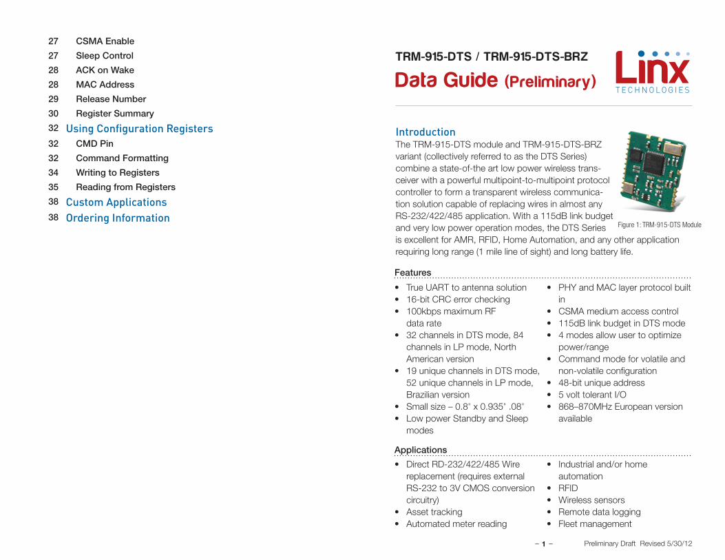
IntroductionThe TRM-915-DTS module and TRM-915-DTS-BRZ variant (collectively referred to as the DTS Series) combine a state-of-the art low power wireless trans-ceiver with a powerful multipoint-to-multipoint protocol controller to form a transparent wireless communica-tion solution capable of replacing wires in almost any RS-232/422/485 application. With a 115dB link budget and very low power operation modes, the DTS Series is excellent for AMR, RFID, Home Automation, and any other application requiring long range (1 mile line of sight) and long battery life.
TRM-915-DTS / TRM-915-DTS-BRZ
Data Guide (Preliminary)
1 Revised 5/30/12Preliminary Draft
Figure 1: TRM-915-DTS Module
27 CSMA Enable
27 Sleep Control
28 ACK on Wake
28 MAC Address
29 Release Number
30 Register Summary
32 Using Configuration Registers32 CMD Pin
32 Command Formatting
34 Writing to Registers
35 Reading from Registers
38 Custom Applications38 Ordering Information
• True UART to antenna solution• 16-bit CRC error checking• 100kbps maximum RF
data rate• 32 channels in DTS mode, 84
channels in LP mode, North American version
• 19 unique channels in DTS mode, 52 unique channels in LP mode, Brazilian version
• Small size – 0.8" x 0.935" .08"• Low power Standby and Sleep
modes
• PHY and MAC layer protocol built in
• CSMA medium access control• 115dB link budget in DTS mode• 4 modes allow user to optimize
power/range• Command mode for volatile and
non-volatile configuration• 48-bit unique address• 5 volt tolerant I/O• 868–870MHz European version
available
Features
Applications
• Direct RD-232/422/485 Wire replacement (requires external RS-232 to 3V CMOS conversion circuitry)
• Asset tracking• Automated meter reading
• Industrial and/or home automation
• RFID• Wireless sensors• Remote data logging• Fleet management
– – – –2
Electrical Specifications
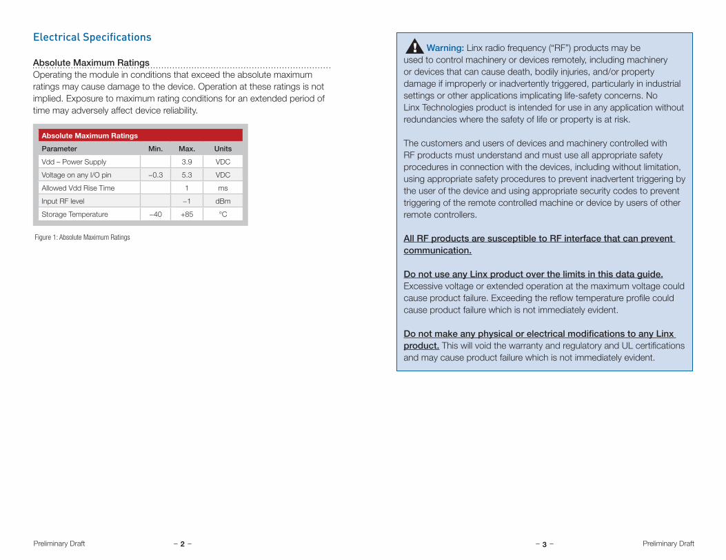
Absolute Maximum RatingsOperating the module in conditions that exceed the absolute maximum ratings may cause damage to the device. Operation at these ratings is not implied. Exposure to maximum rating conditions for an extended period of time may adversely affect device reliability.
Absolute Maximum Ratings
Parameter Min. Max. Units
Vdd – Power Supply 3.9 VDC
Voltage on any I/O pin −0.3 5.3 VDC
Allowed Vdd Rise Time 1 ms
Input RF level −1 dBm
Storage Temperature −40 +85 °C
Figure 1: Absolute Maximum Ratings
Warning: Linx radio frequency (“RF”) products may be used to control machinery or devices remotely, including machinery or devices that can cause death, bodily injuries, and/or property damage if improperly or inadvertently triggered, particularly in industrial settings or other applications implicating life-safety concerns. No Linx Technologies product is intended for use in any application without redundancies where the safety of life or property is at risk.
The customers and users of devices and machinery controlled with RF products must understand and must use all appropriate safety procedures in connection with the devices, including without limitation, using appropriate safety procedures to prevent inadvertent triggering by the user of the device and using appropriate security codes to prevent triggering of the remote controlled machine or device by users of other remote controllers.
All RF products are susceptible to RF interface that can prevent communication.
Do not use any Linx product over the limits in this data guide. Excessive voltage or extended operation at the maximum voltage could cause product failure. Exceeding the reflow temperature profile could cause product failure which is not immediately evident.
Do not make any physical or electrical modifications to any Linx product. This will void the warranty and regulatory and UL certifications and may cause product failure which is not immediately evident.
!
3Preliminary Draft Preliminary Draft
– – – –
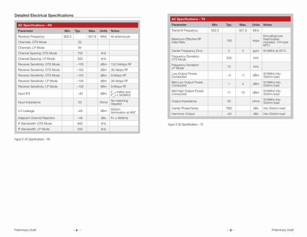
Detailed Electrical Specifications
AC Specifications – RX
Parameter Min. Typ. Max. Units Notes
Receiver Frequency 902.2 927.8 MHz At antenna pin
Channels: DTS Mode 32
Channels: LP Mode 84
Channel Spacing: DTS Mode 750 kHz
Channel Spacing: LP Mode 300 kHz
Receiver Sensitivity: DTS Mode −100 dBm 152.34kbps RF
Receiver Sensitivity: DTS Mode −102 dBm 38.4kbps RF
Receiver Sensitivity: DTS Mode −104 dBm 9.6kbps RF
Receiver Sensitivity: LP Mode −104 dBm 38.4kbps RF
Receiver Sensitivity: LP Mode −105 dBm 9.6kbps RF
Input IP3 −40 dBm FLO+1MHz and FLO+1.945MHz
Input Impedance 50 Ohms No matching required
LO Leakage −65 dBm 50ohm termination at ANT
Adjacent Channel Rejection –48 dBc Fc ± 650kHz
IF Bandwidth: DTS Mode 600 kHz
IF Bandwidth: LP Mode 200 kHz
Figure 2: AC Specifications – RX
4
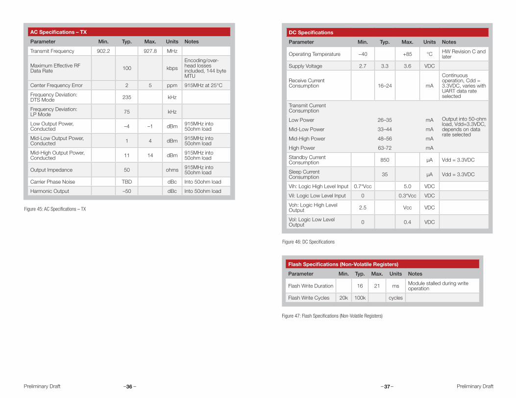
AC Specifications – TX
Parameter Min. Typ. Max. Units Notes
Transmit Frequency 902.2 927.8 MHz
Maximum Effective RF Data Rate 100 kbps
Encoding/over-head losses included, 144 byte MTU
Center Frequency Error 2 5 ppm 915MHz at 25°C
Frequency Deviation:DTS Mode 235 kHz
Frequency Eeviation: LP Mode 75 kHz
Low Output Power, Conducted –4 –1 dBm 915MHz into
50ohm load
Mid-Low Output Power, Conducted 1 4 dBm 915MHz into
50ohm load
Mid-High Output Power, Conducted 11 14 dBm 915MHz into
50ohm load
Output Impedance 50 ohms 915MHz into 50ohm load
Carrier Phase Noise TBD dBc Into 50ohm load
Harmonic Output –50 dBc Into 50ohm load
Figure 3: AC Specifications – TX
5Preliminary Draft Preliminary Draft
– – – –
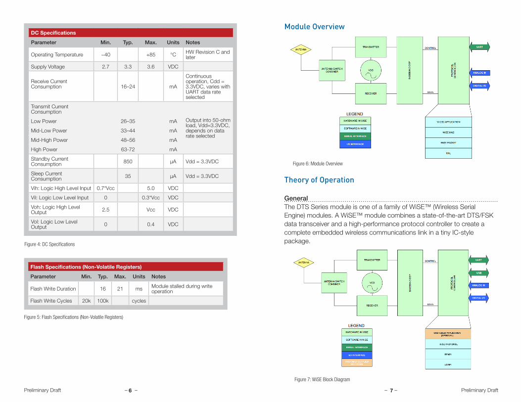
Flash Specifications (Non-Volatile Registers)
Parameter Min. Typ. Max. Units Notes
Flash Write Duration 16 21 ms Module stalled during write operation
Flash Write Cycles 20k 100k cycles
Figure 5: Flash Specifications (Non-Volatile Registers)
DC Specifications
Parameter Min. Typ. Max. Units Notes
Operating Temperature −40 +85 °C HW Revision C and later
Supply Voltage 2.7 3.3 3.6 VDC
Receive Current Consumption 16–24 mA
Continuous operation, Cdd = 3.3VDC, varies with UART data rate selected
Transmit Current Consumption
Output into 50-ohm load, Vdd=3.3VDC, depends on data rate selected
Low Power 26–35 mA
Mid-Low Power 33–44 mA
Mid-High Power 48–56 mA
High Power 63-72 mA
Standby Current Consumption 850 µA Vdd = 3.3VDC
Sleep Current Consumption 35 µA Vdd = 3.3VDC
Vih: Logic High Level Input 0.7*Vcc 5.0 VDC
Vil: Logic Low Level Input 0 0.3*Vcc VDC
Voh: Logic High Level Output 2.5 Vcc VDC
Vol: Logic Low Level Output 0 0.4 VDC
Figure 4: DC Specifications
6
Theory of Operation
GeneralThe DTS Series module is one of a family of WiSE™ (Wireless Serial Engine) modules. A WiSE™ module combines a state-of-the-art DTS/FSK data transceiver and a high-performance protocol controller to create a complete embedded wireless communications link in a tiny IC-style package.
Figure 7: WiSE Block Diagram
Figure 6: Module Overview
Module Overview
7Preliminary Draft Preliminary Draft
– – – –
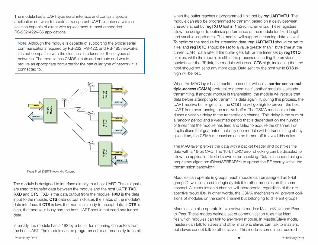
Note: Although the module is capable of supporting the typical serial communications required by RS-232, RS-422, and RS-485 networks, it is not compatible with the electrical interfaces for these types of networks. The module has CMOS inputs and outputs and would require an appropriate converter for the particular type of network it is connected to.
Figure 8: Wi.232DTS Networking Concept
The module is designed to interface directly to a host UART. Three signals are used to transfer data between the module and the host UART: TXD, RXD and CTS. TXD is the data output from the module. RXD is the datainput to the module. CTS data output indicates the status of the module’s data interface. If CTS is low, the module is ready to accept data. If CTS is high, the module is busy and the host UART should not send any further data.
Internally, the module has a 192 byte buffer for incoming characters from the host UART. The module can be programmed to automatically transmit
The module has a UART-type serial interface and contains special application software to create a transparent UART-to-antenna wireless solution capable of direct wire replacement in most embedded RS-232/422/485 applications.
8
when the buffer reaches a programmed limit, set by regUARTMTU. Themodule can also be programmed to transmit based on a delay between characters, set by regTXTO (set in 1mSec increments). These registers allow the designer to optimize performance of the module for fixed lengthand variable length data. The module will support streaming data, as well. To optimize the module for streaming data, regUARTMTU should be set to 144, and regTXTO should be set to a value greater than 1 byte time at thecurrent UART data rate. If the buffer gets full, or the timer set by regTXTO expires, while the module is still in the process of sending the previous packet over the RF link, the module will assert CTS high, indicating that the host should not send any more data. Data sent by the host while CTS is high will be lost.
When the MAC layer has a packet to send, it will use a carrier-sense-mul-tiple-access (CSMA) protocol to determine if another module is already transmitting. If another module is transmitting, the module will receive thatdata before attempting to transmit its data again. If, during this process, the UART receive buffer gets full, the CTS line will go high to prevent the host UART from over-running the receive buffer. The CSMA mechanism intro-duces a variable delay to the transmission channel. This delay is the sum of a random period and a weighted period that is dependent on the number of times that the module has tried and failed to acquire the channel. Forapplications that guarantee that only one module will be transmitting at any given time, the CSMA mechanism can be turned off to avoid this delay.
The MAC layer prefixes the data with a packet header and postfixes the data with a 16-bit CRC. The 16-bit CRC error checking can be disabled to allow the application to do its own error checking. Data is encoded using aproprietary algorithm (DirectSPREAD™) to spread the RF energy within the transmission bandwidth.
Modules can operate in groups. Each module can be assigned an 8-bit group ID, which is used to logically link it to other modules on the same channel. All modules on a channel will interoperate, regardless of their re-spective group IDs. In other words, the CSMA mechanism will prevent colli-sions of modules on the same channel but belonging to different groups.
Modules can also operate in two network modes: Master/Slave and Peer-to-Peer. These modes define a set of communication rules that identi-fies which modules can talk to any given module. In Master/Slave mode, masters can talk to slaves and other masters, slaves can talk to masters, but slaves cannot talk to other slaves. This mode is sometimes required
9Preliminary Draft Preliminary Draft
– – – –
for applications that are replacing legacy RS-485 networks. In peer-to-peer mode, any module can hear any other module. In both modes, group integrity is enforced.
When a module transmits a packet, all other modules on the same channel will receive the packet, check the packet for errors, and determine whether the received group ID matches the local group ID. If the packet is errorfree and the group IDs match, the module will decrypt the data if neces-sary, and send the error free data to its host UART for processing. The modules only implement the ISO reference network stack up to the MAC layer, so they are transparent to link layer addressing schemes. Therefore, the modules can work with any link-layer and higher protocols in existence today.
Certain features of the module are controlled through programmable regis-ters. Registers are accessed by bringing CMD low. When CMD is low, all data transfers from the host UART are considered to be register accesscommands. When CMD is high, all data transfers from the host UART are considered to be raw data that needs to be transparently transmitted across the wireless link. The module maintains two copies of each register: one in flash and one in RAM. On reset, the module loads the RAM registers from the values in the flash registers. The module is operated out of the RAM registers. Applications that need to change parameters of the module often would simply modify the RAM registers. Putting default settings in the flash registers ensures the module always comes up in a preconfigured state, which is useful for applications that do not have external microcontrollers, such as RS-232 adapters.
The UART interface is capable of operating in full duplex at baud rates from 2.4 to 115.2kbps.
The module has ten power modes: High LP, Mid-High LP, Mid-Low LP, Low DTS, High DTS, Mid-High DTS, Mid-Low DTS, Low LP, Standby, and Sleep.
The DTS Series is the first module in the world to take advantage of the DTS digital spread spectrum provision in FCC part 15 rules. Under this provision, transmitters can operate at a higher output power if thetransmission bandwidth is at least 500kHz. Through an encoding technique we call DirectSPREAD™, the outgoing RF data is encoded with symbols selected to ensure its average duty cycle is 50%. This allows the
module to be able to operate at +11dBm and meet the requirements of this provision.
In DTS mode, the module’s channel bandwidth is set to 600kHz and the transmit power is set to one of four selectable levels. In this mode, the module can operate on 32 channels and support a maximum effective RFdata rate of 100kbps. The receiver sensitivity at the max data rate is −100dBm typical, yielding a link budget of 111dB. This mode is an excellent alternative to Frequency Hopping Spread Spectrum. It has no synchronization requirements, allowing it to operate in a duty-cycle mode for extended battery life.
In low-power (LP) mode, the module’s channel bandwidth is set to 200kHz and the transmit power is set to one of four selectable levels. In this mode, the module can operate on 84 channels and support a maximum data rate of 19.2kbps. The receiver sensitivity at the maximum data rate is –105dBm typical, yielding a link budget of 102dB. This mode reduces transmit current consumption, allowing use with batteries that cannot supply the pulse currents required for DTS mode. The range in this mode will be a little more than half of the range in DTS mode. Power settings other than low are available in LP mode, but should only be used when the antenna circuit is lossy.
If the current draw in sleep mode is too high for a particular application, the designer can switch power to the module through a FET to “turn-off” the module when it is not needed. If this technique is used, the volatile registers will reset to the values in their non-volatile mirrors, so any changes from the default will have to be reloaded.
The DTS Series is a very flexible module because of all of the configurable parameters it supports. However, modules that are not configured in the same way will not be able to communicate reliably, causing poorperformance or outright failure of the wireless link. All modules in a network must have the same mode configuration to ensure interoperability.
Every module has read-only internal registers that contain factory programmed information that includes calibration data and a 48-bit
Note: When in sleep mode, the module will not be able to receive data from other modules. Any data sent to the module while it is in sleep mode will be lost.
10 11Preliminary Draft Preliminary Draft
– – – –
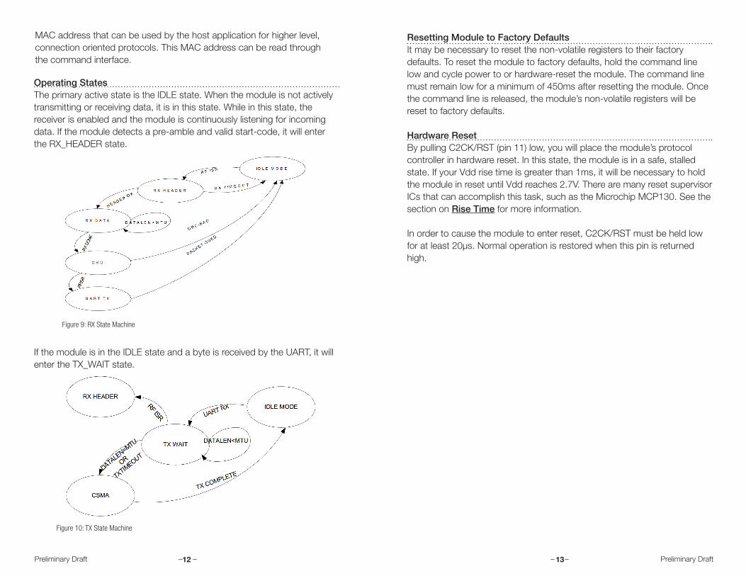
Operating StatesThe primary active state is the IDLE state. When the module is not actively transmitting or receiving data, it is in this state. While in this state, the receiver is enabled and the module is continuously listening for incoming data. If the module detects a pre-amble and valid start-code, it will enter the RX_HEADER state.
If the module is in the IDLE state and a byte is received by the UART, it will enter the TX_WAIT state.
Figure 9: RX State Machine
Figure 10: TX State Machine
MAC address that can be used by the host application for higher level, connection oriented protocols. This MAC address can be read through the command interface.
12
Resetting Module to Factory DefaultsIt may be necessary to reset the non-volatile registers to their factory defaults. To reset the module to factory defaults, hold the command line low and cycle power to or hardware-reset the module. The command line must remain low for a minimum of 450ms after resetting the module. Once the command line is released, the module’s non-volatile registers will be reset to factory defaults.
Hardware ResetBy pulling C2CK/RST (pin 11) low, you will place the module’s protocol controller in hardware reset. In this state, the module is in a safe, stalled state. If your Vdd rise time is greater than 1ms, it will be necessary to hold the module in reset until Vdd reaches 2.7V. There are many reset supervisor ICs that can accomplish this task, such as the Microchip MCP130. See the section on Rise Time for more information.
In order to cause the module to enter reset, C2CK/RST must be held low for at least 20µs. Normal operation is restored when this pin is returned high.
13Preliminary Draft Preliminary Draft
– – – –
Application Information
Pin-out Diagram
Pin Descriptions
No. Description
1 Ground
2 No connect – reserved
3 No connect – reserved
4 Command input – active low
5 UART receive input
6 UART transmit output
7 UART clear to send output – active low
8 No connect – reserve
9 No connect – reserve
10 Reserved – ISP pin C2D
11 ISP pin C2CK/RST
12 Ground
13 Antenna port – 50ohm
14 Ground
15 Ground
16 Ground
17 Ground
18 Ground
19 VCC – 2.7 to 3.6 VDC
Figure 12: Pin Descriptions
Legend
Signals used in this implementation
Signals not used in this implementation – do not connect
Signals used for in-system programming
Figure 11: Pinout Diagram
14
Mechanical Drawings
Figure 13: Module Mechanical Drawings
15Preliminary Draft Preliminary Draft
Pin Descriptions
– – – –
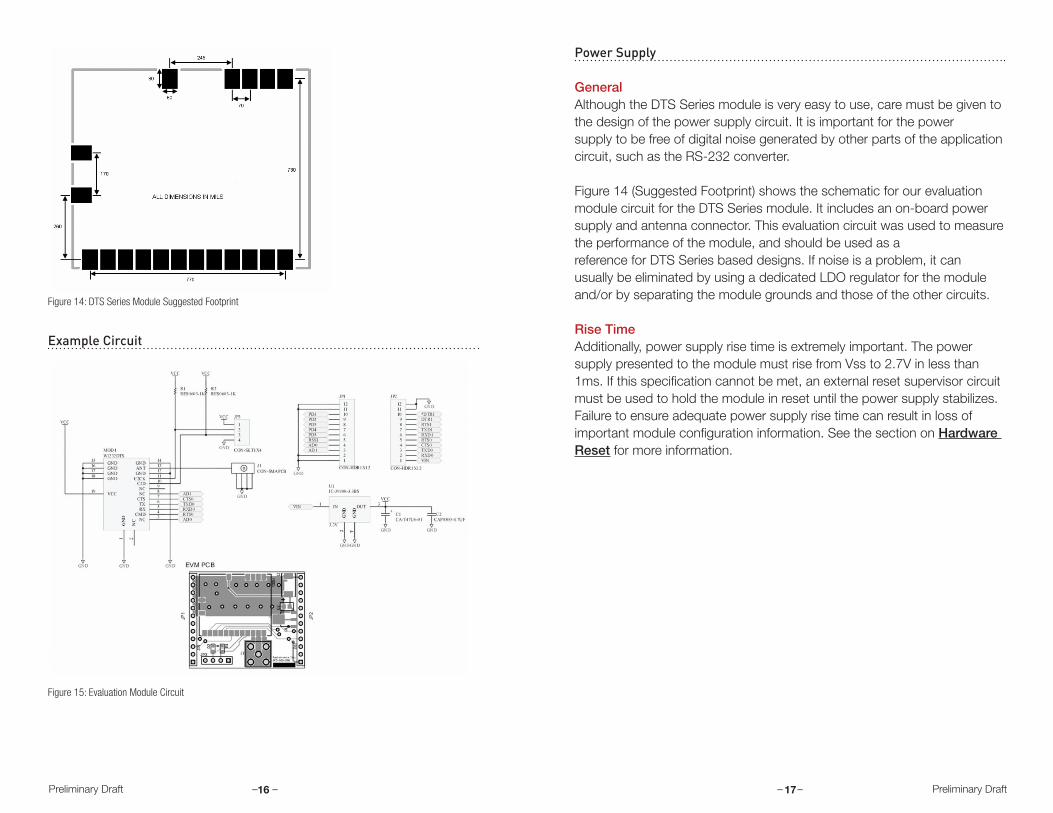
Figure 14: DTS Series Module Suggested Footprint
Example Circuit
Figure 15: Evaluation Module Circuit
16
Power Supply
GeneralAlthough the DTS Series module is very easy to use, care must be given to the design of the power supply circuit. It is important for the power supply to be free of digital noise generated by other parts of the application circuit, such as the RS-232 converter.
Figure 14 (Suggested Footprint) shows the schematic for our evaluation module circuit for the DTS Series module. It includes an on-board power supply and antenna connector. This evaluation circuit was used to measure the performance of the module, and should be used as a reference for DTS Series based designs. If noise is a problem, it can usually be eliminated by using a dedicated LDO regulator for the module and/or by separating the module grounds and those of the other circuits.
Rise TimeAdditionally, power supply rise time is extremely important. The power supply presented to the module must rise from Vss to 2.7V in less than 1ms. If this specification cannot be met, an external reset supervisor circuit must be used to hold the module in reset until the power supply stabilizes. Failure to ensure adequate power supply rise time can result in loss of important module configuration information. See the section on Hardware Reset for more information.
17Preliminary Draft Preliminary Draft
– – – –
UART InterfaceThe UART interface is very simple; it is comprised of four CMOS compatible digital lines.
Pin Description
Line Direction Description
CTS OutClear to send – this pin indicates to the host micro when it is ok to send data. When CTS is high, the host micro should stop sending data to the module until CTS returns to the low state.
CMD In
Command – the host micro will bring this pin low to put the module in command mode. Command mode is used to set and read the internal registers that control the operation of the module.When CMD is high, the module will transparently transfer data to and from other modules on the same channel. NOTE: If this pin is low when the module comes out of reset,the non-volatile registers will be reset to their factory programmed defaults. It is important to ensure that CMD is held high or left floating during power-up under normal conditions.
RXD In Receive data input.
TXD Out Transmit data output.
Figure 16: DTS Series UART Interface Lines
AntennaThe module is designed to work with any 900MHz 50ohm antenna, including PCB trace antennas.
Antenna selection is usually governed by application requirements. In general, external antennas perform better. Linx Technologies has a line of antennas and connectors that are compatible with the modules. Information on these products is available on our website at www.linxtechnologies.com/antennas.
As a rule, a ¼ wave whip or ½ wave dipole antenna with a good, solid ground plane (well-coupled, 3.5" x 3.5" or larger is optimal) is the best choice. Dipoles yield better performance than monopoles (whip) when the ground plane is smaller than optimal. However, many embedded applications cannot support an externally mountedantenna. If this is the case, a PCB antenna must be used. The designer can either use an off-of-the-shelf PCB antenna, such as the ANT-915-SP, or design a trace anten-na. There are several good antenna tutorials and references on the Internet and we encourage the designer to use these resources.
18
Link Budget, Transmit Power and Range PerformanceA link budget is the best figure of merit for comparing wireless solutions and determining how they will perform in the field.
In general, the solution with the best link budget will deliver the best line-of-sight range performance. Improving the link budget by increasing the receiver sensitivity will result in lower power consumption, whileimproving the link budget by increasing the transmit power will result in a more robust performance in the presence of an on-channel interferer or multi-path interference.
The transmit power on unlicensed devices is regulated by the FCC. For transmitters that are not spread-spectrum, the output power is limited to 0dBm (1mW) when a standard ¼ wave whip antenna is used. If the transmitter operates under the spread-spectrum rules, however, the transmit power can be increased; up to 1W depending on the spread-spectrum technique and antennas that are used.
Wireless Fact: Frequency Hopping Spread Spectrum combats in-channel interference, but at the expense of bandwidth, power consumption, and latency. Direct Sequence Spread Spectrum does a better job than FHSS atcombating in-channel interference, but at the expensive of occupied band-width and power consumption. These spread spectrum techniques are generally chosen because the FCC will allow higher output power from atransmitter employing these techniques. Recently, the FCC rules changed to include a new type of spread spectrum device, called Digital Transmis-sion System (DTS). This method of spread spectrum has no processinggain, but allows lower cost solutions like the DTS Series to transmit with higher output power.
To calculate the link budget for a wireless link, simply add the transmit power, the antenna gains and the receiver sensitivity:
LB = Ptx + Gtxa – SENSrx + Grxa
Note: Antenna design is difficult and can be impossible without the proper test equipment. As such, we strongly encourage all of our customers to use off-of-the-shelf antennas whenever possible.
19Preliminary Draft Preliminary Draft
– – – –
For example, the link budget for a pair of modules in DTS mode at the maximum data rate and using 3dBi dipole antennas would be: +11dBm + 3dB – (–100dBm) + 3dB = 117dB
A link budget of 117dB should easily yield a range of ¼ mile or more outdoors. If the environment is open and the antennas are 8 to 10 feet off of the ground, the range could be a mile. Indoors, this link budget should yield a range of several hundred feet.
This is a well-balanced link budget. More than 10dB of the budget is achieved through transmit power, which will allow good performance indoors in the presence of multi-path while keeping the overall operating current low, making the module suitable for primary battery powered applications such as RFID and automated meter reading.
20
Module Configuration
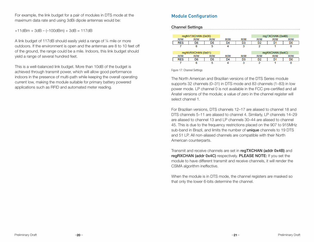
Channel Settings
The North American and Brazilian versions of the DTS Series module supports 32 channels (0–31) in DTS mode and 83 channels (1–83) in low power mode. LP channel 0 is not available in the FCC pre-certified and all Anatel versions of the module; a value of zero in the channel register will select channel 1.
For Brazilian versions, DTS channels 12–17 are aliased to channel 18 and DTS channels 5–11 are aliased to channel 4. Similarly, LP channels 14–29 are aliased to channel 13 and LP channels 30–44 are aliased to channel 45. This is due to the frequency restrictions placed on the 907 to 915MHz sub-band in Brazil, and limits the number of unique channels to 19 DTS and 51 LP. All non-aliased channels are compatible with their North American counterparts.
Transmit and receive channels are set in regTXCHAN (addr 0x4B) and regRXCHAN (addr 0x4C) respectively. PLEASE NOTE: If you set the module to have different transmit and receive channels, it will render the CSMA algorithm ineffective.
When the module is in DTS mode, the channel registers are masked so that only the lower 6-bits determine the channel.
21
Figure 17: Channel Settings
Preliminary Draft Preliminary Draft
– – – –
The following equations can be used to calculate transmit center frequency in LP and DTS modes,remembering the exceptions listed above for the Anatel versions.
Fc = 902.271 + chan *.3007MHz(LP)Fc = 902.272 + chan*.7517MHz(DTS)
All modules in a network must be in the same mode (LP or DTS) and must have the same transmit and receive channels programmed in order to communicate properly.
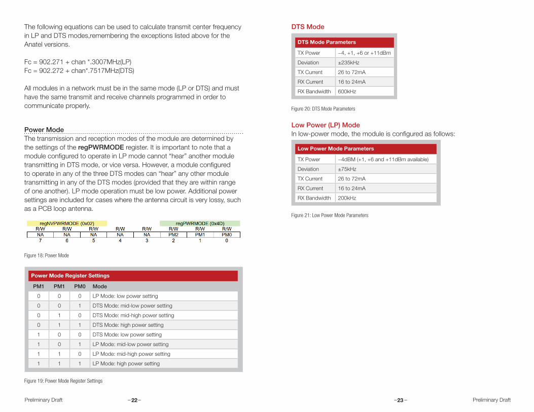
Power ModeThe transmission and reception modes of the module are determined by the settings of the regPWRMODE register. It is important to note that a module configured to operate in LP mode cannot “hear” another module transmitting in DTS mode, or vice versa. However, a module configured to operate in any of the three DTS modes can “hear” any other module transmitting in any of the DTS modes (provided that they are within range of one another). LP mode operation must be low power. Additional power settings are included for cases where the antenna circuit is very lossy, such as a PCB loop antenna.
Power Mode Register Settings
PM1 PM1 PM0 Mode
0 0 0 LP Mode: low power setting
0 0 1 DTS Mode: mid-low power setting
0 1 0 DTS Mode: mid-high power setting
0 1 1 DTS Mode: high power setting
1 0 0 DTS Mode: low power setting
1 0 1 LP Mode: mid-low power setting
1 1 0 LP Mode: mid-high power setting
1 1 1 LP Mode: high power setting
Figure 19: Power Mode Register Settings
Figure 18: Power Mode
22
DTS Mode Parameters
TX Power −4, +1, +6 or +11dBm
Deviation ±235kHz
TX Current 26 to 72mA
RX Current 16 to 24mA
RX Bandwidth 600kHz
Figure 20: DTS Mode Parameters
DTS Mode
Low Power (LP) ModeIn low-power mode, the module is configured as follows:
Low Power Mode Parameters
TX Power −4dBM (+1, +6 and +11dBm available)
Deviation ±75kHz
TX Current 26 to 72mA
RX Current 16 to 24mA
RX Bandwidth 200kHz
Figure 21: Low Power Mode Parameters
23Preliminary Draft Preliminary Draft
– – – –
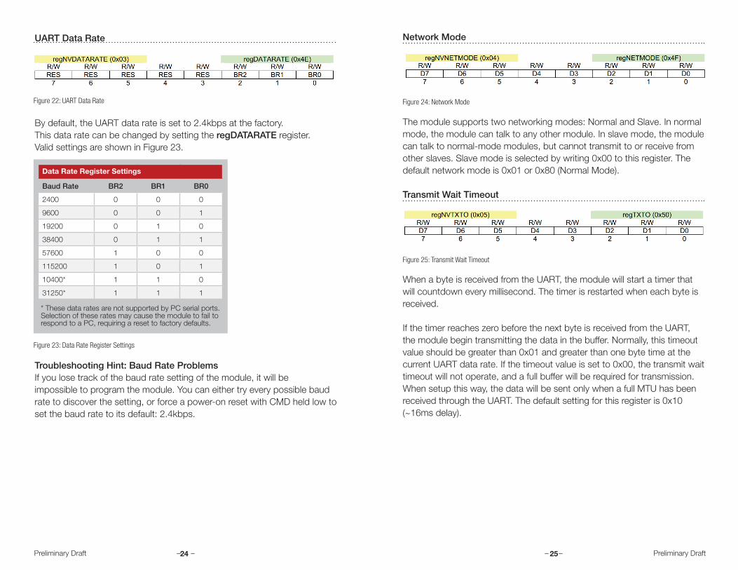
UART Data Rate
By default, the UART data rate is set to 2.4kbps at the factory. This data rate can be changed by setting the regDATARATE register. Valid settings are shown in Figure 23.
Troubleshooting Hint: Baud Rate ProblemsIf you lose track of the baud rate setting of the module, it will be impossible to program the module. You can either try every possible baud rate to discover the setting, or force a power-on reset with CMD held low to set the baud rate to its default: 2.4kbps.
24
Figure 22: UART Data Rate
Data Rate Register Settings
Baud Rate BR2 BR1 BR0
2400 0 0 0
9600 0 0 1
19200 0 1 0
38400 0 1 1
57600 1 0 0
115200 1 0 1
10400* 1 1 0
31250* 1 1 1
Figure 23: Data Rate Register Settings
* These data rates are not supported by PC serial ports. Selection of these rates may cause the module to fail to respond to a PC, requiring a reset to factory defaults.
Network Mode
The module supports two networking modes: Normal and Slave. In normal mode, the module can talk to any other module. In slave mode, the module can talk to normal-mode modules, but cannot transmit to or receive from other slaves. Slave mode is selected by writing 0x00 to this register. The default network mode is 0x01 or 0x80 (Normal Mode).
Transmit Wait Timeout
When a byte is received from the UART, the module will start a timer that will countdown every millisecond. The timer is restarted when each byte is received.
If the timer reaches zero before the next byte is received from the UART, the module begin transmitting the data in the buffer. Normally, this timeout value should be greater than 0x01 and greater than one byte time at the current UART data rate. If the timeout value is set to 0x00, the transmit wait timeout will not operate, and a full buffer will be required for transmission. When setup this way, the data will be sent only when a full MTU has been received through the UART. The default setting for this register is 0x10 (~16ms delay).
Figure 24: Network Mode
Figure 25: Transmit Wait Timeout
25Preliminary Draft Preliminary Draft
– – – –
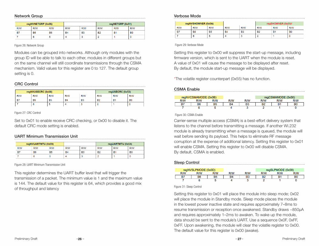
Network Group
Modules can be grouped into networks. Although only modules with the group ID will be able to talk to each other, modules in different groups but on the same channel will still coordinate transmissions through the CSMA mechanism. Valid values for this register are 0 to 127. The default group setting is 0.
CRC Control
Set to 0x01 to enable receive CRC checking, or 0x00 to disable it. The default CRC mode setting is enabled.
UART Minimum Transmission Unit
This register determines the UART buffer level that will trigger the transmission of a packet. The minimum value is 1 and the maximum value is 144. The default value for this register is 64, which provides a good mix of throughput and latency
Figure 26: Network Group
Figure 27: CRC Control
Figure 28: UART Minimum Transmission Unit
26
Verbose Mode
Setting this register to 0x00 will suppress the start-up message, including firmware version, which is sent to the UART when the module is reset. A value of 0x01 will cause the message to be displayed after reset. By default, the module start-up message will be displayed.
*The volatile register counterpart (0x55) has no function.
CSMA Enable
Carrier-sense multiple access (CSMA) is a best-effort delivery system that listens to the channel before transmitting a message. If another Wi.232 module is already transmitting when a message is queued, the module will wait before sending its payload. This helps to eliminate RF message corruption at the expense of additional latency. Setting this register to 0x01 will enable CSMA. Setting this register to 0x00 will disable CSMA. By default, CSMA is enabled.
Sleep Control
Setting this register to 0x01 will place the module into sleep mode; 0x02 will place the module in Standby mode. Sleep mode places the module in the lowest power inactive state and requires approximately 7–8ms to resume transmission or reception once awakened. Standby draws ~850µA and requires approximately 1–2ms to awaken. To wake up the module, data should be sent to the module’s UART. Use a sequence 0x0F, 0xFF, 0xFF. Upon awakening, the module will clear the volatile register to 0x00. The default value for this register is 0x00 (awake).
Figure 30: CSMA Enable
Figure 31: Sleep Control
Figure 29: Verbose Mode
27Preliminary Draft Preliminary Draft
– – – –
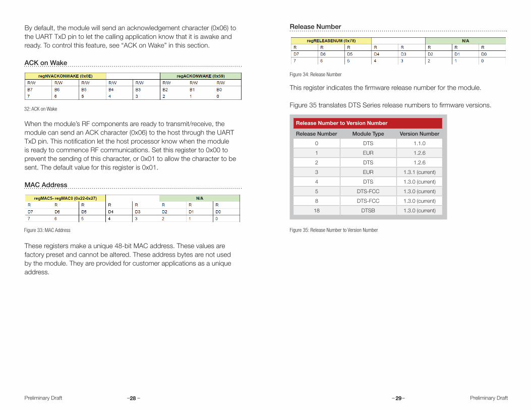
By default, the module will send an acknowledgement character (0x06) to the UART TxD pin to let the calling application know that it is awake and ready. To control this feature, see “ACK on Wake” in this section.
ACK on Wake
When the module’s RF components are ready to transmit/receive, the module can send an ACK character (0x06) to the host through the UART TxD pin. This notification let the host processor know when the module is ready to commence RF communications. Set this register to 0x00 to prevent the sending of this character, or 0x01 to allow the character to be sent. The default value for this register is 0x01.
MAC Address
These registers make a unique 48-bit MAC address. These values are factory preset and cannot be altered. These address bytes are not used by the module. They are provided for customer applications as a unique address.
Figure 33: MAC Address
32: ACK on Wake
28
Release Number
This register indicates the firmware release number for the module. Figure 35 translates DTS Series release numbers to firmware versions.
Figure 34: Release Number
Release Number to Version Number
Release Number Module Type Version Number
0 DTS 1.1.0
1 EUR 1.2.6
2 DTS 1.2.6
3 EUR 1.3.1 (current)
4 DTS 1.3.0 (current)
5 DTS-FCC 1.3.0 (current)
8 DTS-FCC 1.3.0 (current)
18 DTSB 1.3.0 (current)
Figure 35: Release Number to Version Number
29Preliminary Draft Preliminary Draft
– – – –
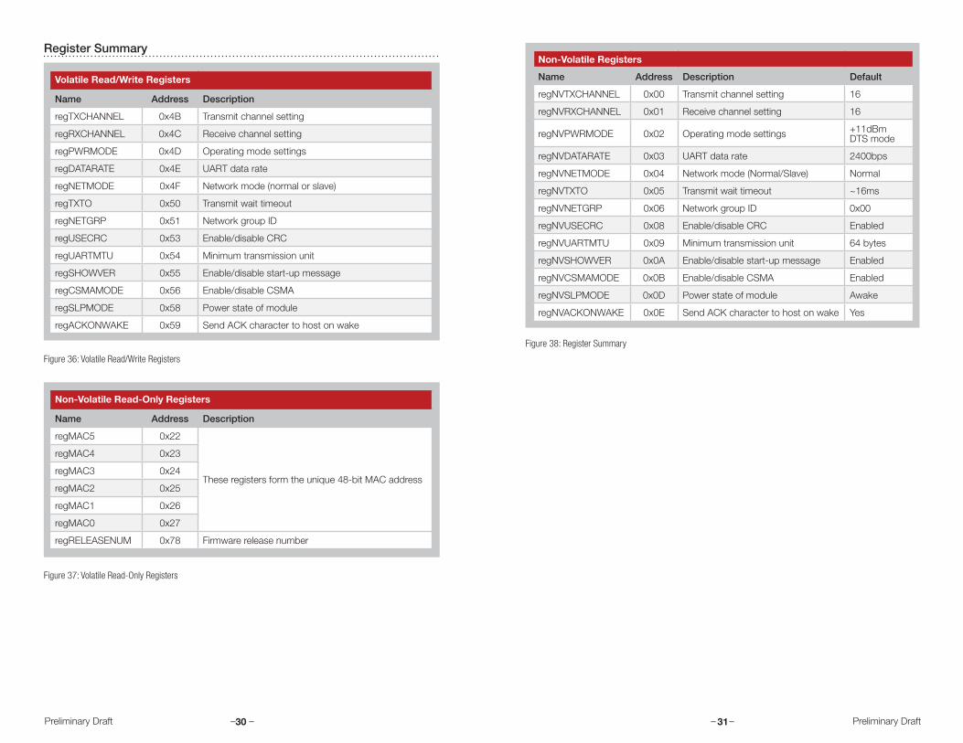
Register Summary
Volatile Read/Write Registers
Name Address Description
regTXCHANNEL 0x4B Transmit channel setting
regRXCHANNEL 0x4C Receive channel setting
regPWRMODE 0x4D Operating mode settings
regDATARATE 0x4E UART data rate
regNETMODE 0x4F Network mode (normal or slave)
regTXTO 0x50 Transmit wait timeout
regNETGRP 0x51 Network group ID
regUSECRC 0x53 Enable/disable CRC
regUARTMTU 0x54 Minimum transmission unit
regSHOWVER 0x55 Enable/disable start-up message
regCSMAMODE 0x56 Enable/disable CSMA
regSLPMODE 0x58 Power state of module
regACKONWAKE 0x59 Send ACK character to host on wake
Non-Volatile Read-Only Registers
Name Address Description
regMAC5 0x22
These registers form the unique 48-bit MAC address
regMAC4 0x23
regMAC3 0x24
regMAC2 0x25
regMAC1 0x26
regMAC0 0x27
regRELEASENUM 0x78 Firmware release number
Figure 36: Volatile Read/Write Registers
Figure 37: Volatile Read-Only Registers
30
Non-Volatile Registers
Name Address Description Default
regNVTXCHANNEL 0x00 Transmit channel setting 16
regNVRXCHANNEL 0x01 Receive channel setting 16
regNVPWRMODE 0x02 Operating mode settings +11dBm DTS mode
regNVDATARATE 0x03 UART data rate 2400bps
regNVNETMODE 0x04 Network mode (Normal/Slave) Normal
regNVTXTO 0x05 Transmit wait timeout ~16ms
regNVNETGRP 0x06 Network group ID 0x00
regNVUSECRC 0x08 Enable/disable CRC Enabled
regNVUARTMTU 0x09 Minimum transmission unit 64 bytes
regNVSHOWVER 0x0A Enable/disable start-up message Enabled
regNVCSMAMODE 0x0B Enable/disable CSMA Enabled
regNVSLPMODE 0x0D Power state of module Awake
regNVACKONWAKE 0x0E Send ACK character to host on wake Yes
Figure 38: Register Summary
31Preliminary Draft Preliminary Draft
– – – –
Command FormattingThe DTS Series module contains several volatile and non-volatile registers that control its configuration and operation. The volatile registers all have a non-volatile mirror registers that are used to determine the defaultconfiguration when power is applied to the module. During normal operation, the volatile registers are used to control the module.
Placing the module in the command mode allows these registers to be programmed. Byte values in excess of 127 (0x80 or greater) must be changed into a two-byte escape sequence of the format: 0xFE, [value - 128]. For example, the value 0x83 becomes 0xFE, 0x03. The follow-ing function will prepend a 0xFF header and size specifier to a command sequence and create escape sequences as needed. It is assumed that *src is populated with either the register number to read (one byte, pass 1 into src_len) or the register number and value to write (two bytes, pass 2 into src_len). It is also assumed that the *dest buffer has enough space for the two header characters plus, the encoded command, and the null terminator.
int EscapeString(char *src, char src_len, char *dest)
{
// The following function copies and encodes the first
// src_len characters from *src into *dest. This
// encoding is necessary for module command formats.
// The resulting string is null terminated. The size
// of this string is the function return value.
// ---------------------------------------------------
char src_idx, dest_idx;
// Save space for the command header and size bytes
// ------------------------------------------------
dest_idx = 2;
// Loop through source string and copy/encode
// ------------------------------------------
for (src_idx = 0; src_idx < src_len; src_idx++)
{
if (src[src_idx] > 127)
{
dest[dest_idx++] = 0xFE;
}/*if*/
dest[dest_idx++] = (src[src_idx] & 0x7F);
}/*for*/
// Add null terminator
// -------------------
dest[dest_idx] = 0;
// Add command header
// ------------------
dest[0] = 0xFF;
dest[1] = dest_idx – 2;
// Return escape string size
// -------------------------
return dest_idx;
}
32
Using Configuration Registers
CMD PinThe CMD pin is used to inform the module where incoming UART information should be routed. When the CMD pin is high or left floating, all incoming UART information is treated as payload data and transferred over the wireless interface. If the CMD pin is low, the incoming UART data is routed to the command parser for processing. Since the module’s proces-sor looks at UART data one byte at a time, the CMD line must be held low for the entire duration of the command plus a 20µs margin for processing. Leaving the CMD pin low for additional time (for example, until the ACK byte is received by your application) will not adversely affect the module. If RF packets are received while the CMD line is active, they are still processed and presented to the module’s UART for transmission.
Figure 39: Command and CMD Pin Timing
Figure 40: Command Conversion Code
33Preliminary Draft Preliminary Draft
– – – –
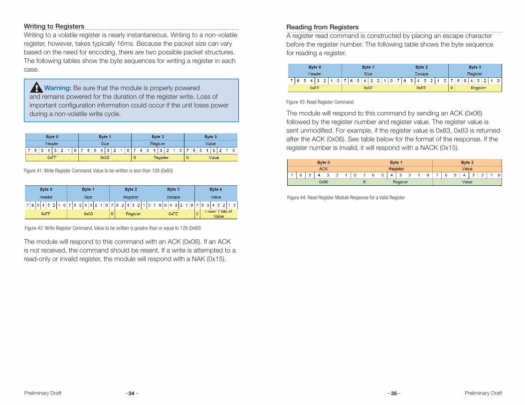
Writing to RegistersWriting to a volatile register is nearly instantaneous. Writing to a non-volatile register, however, takes typically 16ms. Because the packet size can vary based on the need for encoding, there are two possible packet structures. The following tables show the byte sequences for writing a register in each case.
The module will respond to this command with an ACK (0x06). If an ACK is not received, the command should be resent. If a write is attempted to a read-only or invalid register, the module will respond with a NAK (0x15).
Warning: Be sure that the module is properly powered and remains powered for the duration of the register write. Loss of important configuration information could occur if the unit loses power during a non-volatile write cycle.
Figure 41: Write Register Command, Value to be written is less than 128 (0x80)
!
34Preliminary Draft
Figure 42: Write Register Command, Value to be written is greatre than or equal to 128 (0x80)
Reading from RegistersA register read command is constructed by placing an escape character before the register number. The following table shows the byte sequence for reading a register.
The module will respond to this command by sending an ACK (0x06) followed by the register number and register value. The register value is sent unmodified. For example, if the register value is 0x83, 0x83 is returned after the ACK (0x06). See table below for the format of the response. If the register number is invalid, it will respond with a NACK (0x15).
Figure 43: Read Register Command
Figure 44: Read Register Module Response for a Valid Register
35 Preliminary Draft
– – – –
AC Specifications – TX
Parameter Min. Typ. Max. Units Notes
Transmit Frequency 902.2 927.8 MHz
Maximum Effective RF Data Rate 100 kbps
Encoding/over-head losses included, 144 byte MTU
Center Frequency Error 2 5 ppm 915MHz at 25°C
Frequency Deviation:DTS Mode 235 kHz
Frequency Deviation: LP Mode 75 kHz
Low Output Power, Conducted –4 –1 dBm 915MHz into
50ohm load
Mid-Low Output Power, Conducted 1 4 dBm 915MHz into
50ohm load
Mid-High Output Power, Conducted 11 14 dBm 915MHz into
50ohm load
Output Impedance 50 ohms 915MHz into 50ohm load
Carrier Phase Noise TBD dBc Into 50ohm load
Harmonic Output –50 dBc Into 50ohm load
Figure 45: AC Specifications – TX
36Preliminary Draft
Flash Specifications (Non-Volatile Registers)
Parameter Min. Typ. Max. Units Notes
Flash Write Duration 16 21 ms Module stalled during write operation
Flash Write Cycles 20k 100k cycles
Figure 47: Flash Specifications (Non-Volatile Registers)
DC Specifications
Parameter Min. Typ. Max. Units Notes
Operating Temperature −40 +85 °C HW Revision C and later
Supply Voltage 2.7 3.3 3.6 VDC
Receive Current Consumption 16–24 mA
Continuous operation, Cdd = 3.3VDC, varies with UART data rate selected
Transmit Current Consumption
Output into 50-ohm load, Vdd=3.3VDC, depends on data rate selected
Low Power 26–35 mA
Mid-Low Power 33–44 mA
Mid-High Power 48–56 mA
High Power 63-72 mA
Standby Current Consumption 850 µA Vdd = 3.3VDC
Sleep Current Consumption 35 µA Vdd = 3.3VDC
Vih: Logic High Level Input 0.7*Vcc 5.0 VDC
Vil: Logic Low Level Input 0 0.3*Vcc VDC
Voh: Logic High Level Output 2.5 Vcc VDC
Vol: Logic Low Level Output 0 0.4 VDC
Figure 46: DC Specifications
37 Preliminary Draft
– –
Custom ApplicationsFor cost-sensitive applications, such as wireless sensors and AMR, Linx Technologies can embed the application software directly into the microcontroller built into the module. For more information on this service, please contact Linx Technologies.
Ordering Information
Ordering Information
Product Part No. Description Radiotronix Part No.
TRM-915-DTS North American Embedded Wireless Module (902–928Hz) Wi.232DTS-R
TRM-915-DTS-BRZ Brazilian Embedded Wireless Module (902–907, 915–928MHz) Wi.232DTSB-R
TRM-868-EUR European Union Embedded Wireless Module (868–870MHz) WI.232EUR
Figure 48: Ordering Information
Preliminary Draft 38

Linx Technologies
159 Ort Lane
Merlin, OR, US 97532
3090 Sterling Circle, Suite 200
Boulder, CO 80301
Phone: +1 541 471 6256
Fax: +1 541 471 6251
www.linxtechnologies.com
DisclaimerLinx Technologies is continually striving to improve the quality and function of its products. For this reason, we reserve the right to make changes to our products without notice. The information contained in this Data Guide is believed to be accurate as of the time of publication. Specifications are based on representative lot samples. Values may vary from lot-to-lot and are not guaranteed. “Typical” parameters can and do vary over lots and application. Linx Technologies makes no guarantee, warranty, or representation regarding the suitability of any product for use in any specific application. It is Customer’s responsibility to verify the suitability of the part for the intended application. At Customer’s request, Linx Technologies may provide advice and assistance in designing systems and remote control devices that employ Linx Technologies RF products, but responsibility for the ultimate design and use of any such systems and devices remains entirely with Customer and/or user of the RF products.
LINX TECHNOLOGIES DISCLAIMS ANY AND ALL WARRANTIES OF MERCHANTABILITY AND FITNESS FOR A PARTICULAR PURPOSE. IN NO EVENT SHALL LINX TECHNOLOGIES BE LIABLE FOR ANY CUSTOMER’S OR USER’S INCIDENTAL OR CONSEQUENTIAL DAMAGES ARISING OUT OF OR RELATED TO THE DESIGN OR USE OF A REMOTE CONTROL SYSTEM OR DEVICE EMPLOYING LINX TECHNOLOGIES RF PRODUCTS OR FOR ANY OTHER BREACH OF CONTRACT BY LINX TECHNOLOGIES. CUSTOMER AND/OR USER ASSUME ALL RISKS OF DEATH, BODILY INJURIES, OR PROPERTY DAMAGE ARISING OUT OF OR RELATED TO THE USE OF LINX TECHNOLOGIES RF PRODUCTS, INCLUDING WITH RESPECT TO ANY SERVICES PROVIDED BY LINX RELATED TO THE USE OF LINX TECHNOLOGIES RF PRODUCTS. LINX TECHNOLOGIES SHALL NOT BE LIABLE UNDER ANY CIRCUMSTANCES FOR A CUSTOMER’S, USER’S, OR OTHER PERSON’S DEATH, BODILY INJURY, OR PROPERTY DAMAGE ARISING OUT OF OR RELATED TO THE DESIGN OR USE OF A REMOTE CONTROL SYSTEM OR DEVICE EMPLOYING LINX TECHNOLOGIES RF PRODUCTS.
The limitations on Linx Technologies’ liability are applicable to any and all claims or theories of recovery asserted by Customer, including, without limitation, breach of contract, breach of warranty, strict liability, or negligence. Customer assumes all liability (including, without limitation, liability for injury to person or property, economic loss, or business interruption) for all claims, including claims from third parties, arising from the use of the Products. Under no conditions will Linx Technologies be responsible for losses arising from the use or failure of the device in any application, other than the repair, replacement, or refund limited to the original product purchase price. Devices described in this publication may contain proprietary, patented, or copyrighted techniques, components, or materials.
All rights reserved. ©2012 Linx Technologies
The stylized Linx logo, Wireless Made Simple, CipherLinx, WiSE and the stylized CL logo are trademarks of Linx Technologies.