ts 101 524-2 - v1.1.1 - transmission and multiplexing (tm); …€¦ · · 2000-06-23transmission...
TRANSCRIPT

ETSI TS 101 524-2 V1.1.1 (2000-06)Technical Specification
Transmission and Multiplexing (TM);Access transmission system on metallic access cables;
Symmetrical single pair high bit rateDigital Subscriber Line (SDSL);
Part 2: Transceiver requirements

ETSI
ETSI TS 101 524-2 V1.1.1 (2000-06)2
ReferenceDTS/TM-06011-2
KeywordsSDSL, access, adaption, basic, coding, digital,
HDSL, IP, ISDN, local loop, PSTN, rate,subscriber, transmission
ETSI
650 Route des LuciolesF-06921 Sophia Antipolis Cedex - FRANCE
Tel.: +33 4 92 94 42 00 Fax: +33 4 93 65 47 16
Siret N° 348 623 562 00017 - NAF 742 CAssociation à but non lucratif enregistrée à laSous-Préfecture de Grasse (06) N° 7803/88
Important notice
Individual copies of the present document can be downloaded from:http://www.etsi.org
The present document may be made available in more than one electronic version or in print. In any case of existing orperceived difference in contents between such versions, the reference version is the Portable Document Format (PDF).In case of dispute, the reference shall be the printing on ETSI printers of the PDF version kept on a specific network drive
within ETSI Secretariat.
Users of the present document should be aware that the document may be subject to revision or change of status.Information on the current status of this and other ETSI documents is available at http://www.etsi.org/tb/status/
If you find errors in the present document, send your comment to:[email protected]
Copyright Notification
No part may be reproduced except as authorized by written permission.The copyright and the foregoing restriction extend to reproduction in all media.
© European Telecommunications Standards Institute 2000.All rights reserved.

ETSI
ETSI TS 101 524-2 V1.1.1 (2000-06)3
Contents
Intellectual Property Rights ................................................................................................................................4
Foreword.............................................................................................................................................................4
1 Scope ........................................................................................................................................................5
2 References ................................................................................................................................................5
3 Abbreviations ...........................................................................................................................................5
4 PMD Layer Functional Characteristics ....................................................................................................64.1 Activation ...........................................................................................................................................................64.1.1 Activation PMD reference model .................................................................................................................64.1.2 Activation sequence......................................................................................................................................74.1.2.1 Signal Cr ..................................................................................................................................................84.1.2.2 Signal Sc ..................................................................................................................................................84.1.2.3 Signal Sr ..................................................................................................................................................94.1.2.4 Signal Tc..................................................................................................................................................94.1.2.5 Signal Tr ..................................................................................................................................................94.1.2.6 Signal Fc ..................................................................................................................................................94.1.2.7 Datac and Datar........................................................................................................................................94.1.2.8 Exception state ........................................................................................................................................94.1.2.9 Exception condition ................................................................................................................................94.1.3 Activation framer........................................................................................................................................104.1.3.1 Frame sync ............................................................................................................................................104.1.3.2 Precoder coefficients.............................................................................................................................104.1.3.3 Encoder coefficients..............................................................................................................................104.1.3.4 Vendor ID .............................................................................................................................................104.1.3.5 Reserved................................................................................................................................................104.1.3.6 CRC.......................................................................................................................................................114.1.4 Pre-activation Communication Channel (PACC) .......................................................................................114.1.5 Scrambler....................................................................................................................................................114.1.6 Mapper........................................................................................................................................................114.1.7 Spectral shaper............................................................................................................................................114.1.8 Timeouts .....................................................................................................................................................114.2 PMD pre-activation sequence...........................................................................................................................124.2.1 PMD pre-activation reference model ..........................................................................................................124.2.2 PMD pre-activation sequence description ..................................................................................................124.2.2.1 Signal Pri................................................................................................................................................134.2.2.2 Signal Pci ...............................................................................................................................................134.2.3 Scrambler....................................................................................................................................................134.2.4 Mapper........................................................................................................................................................144.2.5 Spectral shaper............................................................................................................................................144.3 Data mode ........................................................................................................................................................144.3.1 Data mode PMD reference model...............................................................................................................144.3.1.1 PMD rates .............................................................................................................................................144.3.2 Scrambler....................................................................................................................................................144.3.3 UC-PAM encoder .......................................................................................................................................154.3.3.1 Serial-to-parallel converter....................................................................................................................154.3.3.2 Convolutional encoder ..........................................................................................................................154.3.3.3 Mapper ..................................................................................................................................................164.3.4 Channel precoder ........................................................................................................................................164.3.5 Spectral shaper............................................................................................................................................174.4 PSD masks........................................................................................................................................................174.4.1 Symmetric PSD masks................................................................................................................................184.4.2 Asymmetric 2 048 kbit/s and 2 304 kbit/s PSD masks ...............................................................................20
History ..............................................................................................................................................................23

ETSI
ETSI TS 101 524-2 V1.1.1 (2000-06)4
Intellectual Property RightsIPRs essential or potentially essential to the present document may have been declared to ETSI. The informationpertaining to these essential IPRs, if any, is publicly available for ETSI members and non-members, and can be foundin ETSI SR 000 314: "Intellectual Property Rights (IPRs); Essential, or potentially Essential, IPRs notified to ETSI inrespect of ETSI standards", which is available from the ETSI Secretariat. Latest updates are available on the ETSI Webserver (http://www.etsi.org/ipr).
Pursuant to the ETSI IPR Policy, no investigation, including IPR searches, has been carried out by ETSI. No guaranteecan be given as to the existence of other IPRs not referenced in ETSI SR 000 314 (or the updates on the ETSI Webserver) which are, or may be, or may become, essential to the present document.
ForewordThis Technical Specification (TS) has been produced by ETSI Technical Committee Transmission and Multiplexing(TM).
The present document is part 2 of a multi-part TS covering Access transmission system on metallic access cables;Symmetrical single pair high bit rate Digital Subscriber Line (SDSL), as identified below:
Part 1: "Functional requirements";
Part 2: "Transceiver Requirements".
ETSI
ETSI TS 101 524-2 V1.1.1 (2000-06)5
1 ScopeThis multi-part TS specifies requirements for transceivers providing bi-directional symmetrical high bit ratetransmission on a single metallic wire pair using the echo cancellation method. The technology is referred to asSymmetrical single-pair high bit rate Digital Subscriber Line (SDSL), and is applicable to metallic access transmissionsystems designed to provide digital access over existing, unshielded wire pairs.
The present document is part 2 of the Technical Specification for SDSL and defines implementation requirements fortransceivers which enable the functional requirements of part 1 to be met.
The requirements addressed imply interoperability of SDSL systems. Such interoperability will be achieved whenSDSL transceivers provided by different manufacturers are used in one SDSL link.
NOTE: It is planned to merge the parts 1 and 2 into a common specification in the coming revision.
2 ReferencesThe following documents contain provisions which, through reference in this text, constitute provisions of the presentdocument.
• References are either specific (identified by date of publication, edition number, version number, etc.) ornon-specific.
• For a specific reference, subsequent revisions do not apply.
• For a non-specific reference, the latest version applies.
• A non-specific reference to an ETS shall also be taken to refer to later versions published as an EN with the samenumber.
[1] ITU-T Recommendation G.994.1: "Handshake procedures for digital subscriber line (DSL)transceivers".
3 AbbreviationsFor the purposes of the present document, the following abbreviations apply:
BER Bit Error RatioBERTS Bit Error Rate Test SetBT Bridged Tap, an unterminated twisted pair section bridged across the lineCRC Cyclic Redundancy CheckDLL Digital Local Lineeoc embedded operations channelEMC Electromagnetic CompatibilityFCS Frame Check SequenceFEXT Far End CrosstalkHDLC High level Data Link ControlHDSL High bit rate Digital Subscriber LineISDN BA Integrated Services Digital Network Basic rate AccessIUT Item Under TestLCL Longitudinal Conversion Losslsb least significant bitLTU Line Termination Unitmsb most significant bitNEXT Near End CrosstalkNTU Network Termination UnitOH OverheadO&M Operation and Maintenance

ETSI
ETSI TS 101 524-2 V1.1.1 (2000-06)6
PACC Pre-activation Communication ChannelPAM Pulse Amplitude ModulationPLL Phase Locked LoopPMD Physical Medium DependentPMS Physical Medium SpecificPRBS Pseudo-Random Bit SequencePSD Power Spectral DensityPSL Power Sum LossREG RegeneratorREG-C NTU side of the regeneratorREG-R LTU side of the regeneratorRF Radio Frequencyrms root mean squareSDH Synchronous Digital HierarchySDSL Symmetric single pair high bit rate Digital Subscriber LineSNR Signal to Noise RatioTC Transmission ConvergenceTC-PAM Trellis Coded Pulse Amplitude ModulationTPS Transmission Protocol SpecificTMN Telecommunication Management NetworkTU-12 Tributary Unit-12UC-PAM Ungerboeck Coded Pulse Amplitude ModulationUTC Unable to complyVC-12 Virtual Container-122B1Q two binary one quaternary line code
4 PMD Layer Functional Characteristics
4.1 ActivationThis subclause describes waveforms at the loop interface and associated procedures during activation mode. The directspecification of the performance of individual receiver elements is avoided when possible. Instead, the transmittercharacteristics are specified on an individual basis and the receiver performance is specified on a general basis as theaggregate performance of all receiver elements. Exceptions are made for cases where the performance of an individualreceiver element is crucial to interoperability.
In subclause 4.1.2 "convergence" refers to the state where all adaptive elements have reached steady-state. Thedeclaration of convergence by a transceiver is therefore vendor dependent. Nevertheless, actions based on the state ofconvergence are specified to improve interoperability.
4.1.1 Activation PMD reference model
The block diagram of the activation mode PMD layer of an LTU or NTU transmitter is shown in figure 1.
ActivationFramer
SpectralShaper
MapperScrambler
d(m)
f(m)
s(m) y(m) z(t)
logicalones
precodercoefficients,
encodercoefficients
output atloop
interface
Figure 1: Activation PMD reference model

ETSI
ETSI TS 101 524-2 V1.1.1 (2000-06)7
The time index m represents the symbol time, and t represents analogue time. Since activation uses 2-PAM modulation,the bit time is equivalent to the symbol time. The output of the framer are the framed information bits f(m). The outputof the scrambler is s(m). The output of the mapper is y(m), and the output of the spectral shaper at the loop interface isz(t). d(m) is an initialization signal that shall be logical ones for all m. The modulation format shall be uncoded 2-PAM,with the full symbol rate selected for data mode operation. During activation the timing reference for the activationsignals have a tolerance of ±32 ppm at the LTU and ±100 ppm at the NTU.
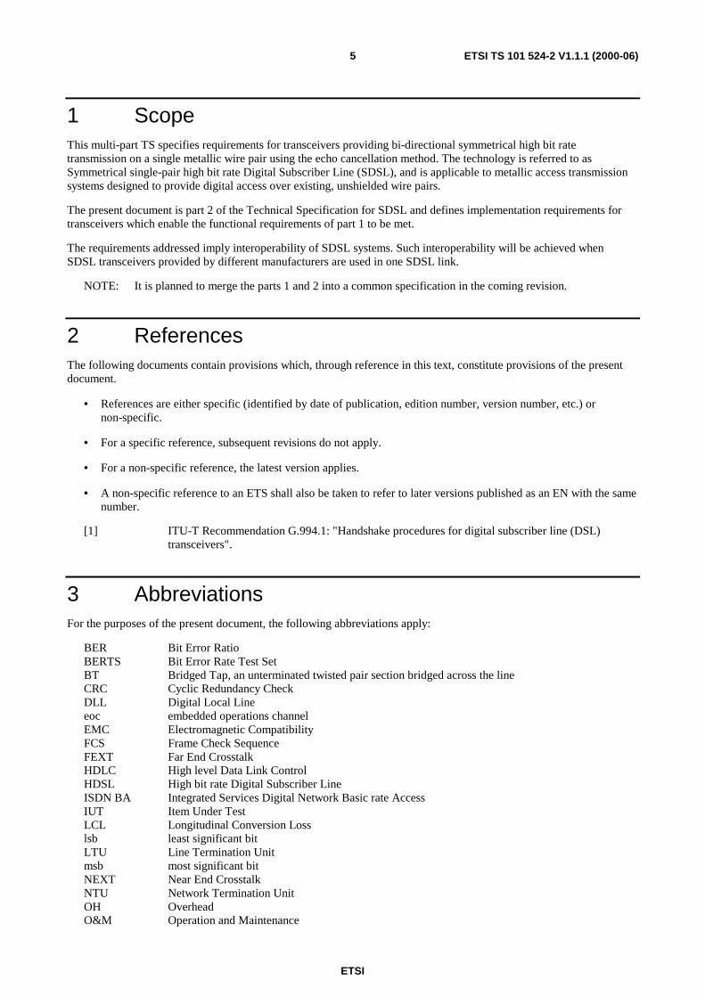
4.1.2 Activation sequence
The timing diagram for the activation sequence is given in figure 2. The state transition diagram for the activationsequence is given in figure 3. Each activation signal in the activation sequence shall satisfy the tolerance values listed intable 1.
NOTE: A warm-start procedure is under study for use in systems that can go into a deactivated state, when nocommunication is going on.
DatarTr
(Units in seconds)
Cr
1
DatacFcTc
TAct
0,5 1
Sr
Sc
Figure 2: Timing Diagram for activation sequence
Table 1: Tolerance values for activation signals
Signal Parameter Reference Nominal Value ToleranceCr duration subclause 4.1.2.1 1 s ±20 msSc time after end of Cr subclause 4.1.2.2 500 ms ±20 msSr time after end of Cr subclause 4.1.2.3 1,5 s ±20 ms
ETSI
ETSI TS 101 524-2 V1.1.1 (2000-06)8
Power-on
Sc
LTU
Cr detected
Receiver convergedon Sr and Sc sent >T PLL
Tc
Tr detected
Fc
DATAc
Exceptionstate
Preactivation
Not convergedon Sr
Tr notdetected
Exceptiondetected
Cr
NTU
Sr
Tc detected
Tr
DATAc
Exceptionstate
Preactivation
Notconvergedon Tc or
Tc notdetected
Exceptiondetected
Fc detected
Fc Notdetected
Power-on
Figure 3: LTU and NTU Transmitter State Transition Diagram
4.1.2.1 Signal Cr
After exiting the pre-activation sequence (see subclause 4.1.4), the NTU shall send Cr. Waveform Cr shall be generatedby connecting the signal d(m) to the input of the NTU scrambler as shown in figure 1. The PSD mask for Cr shall be theupstream PSD mask, as negotiated during pre-activation sequence. Cr shall have a duration of 1 s and shall be sent 0,3 safter the end of pre-activation.
4.1.2.2 Signal Sc
After detecting Cr, the LTU shall send Sc. Waveform Sc shall be generated by connecting the signal d(m) to the input ofthe LTU scrambler as shown in figure 1. The PSD mask for Sc shall be the downstream PSD mask, as negotiated duringpre-activation sequence. Sc shall be sent 0,5 s after the end of Cr. If the LTU does not converge while Sc is transmitted,it shall enter the exception state (subclause 4.1.2.8).

ETSI
ETSI TS 101 524-2 V1.1.1 (2000-06)9
4.1.2.3 Signal Sr
The NTU shall send Sr, beginning 1,5 s after the end of Cr. Waveform Sr shall be generated by connecting the signald(m) to the input of the NTU scrambler as shown in figure 1. The PSD mask for Sr shall be the same as for Cr. If theNTU does not converge and detect Tc while Sr is transmitted, it shall enter the exception state (subclause 4.1.2.8). Themethod used to detect Tc is vendor dependent. In timing modes supporting loop timing, waveform Sr and all subsequentsignals transmitted from the NTU shall be loop timed, i.e., the NTU symbol clock shall be locked to the LTU symbolclock.
4.1.2.4 Signal Tc
Once the LTU has converged and has been sending Sc for at least TPLL seconds (see table 4), it shall send Tc. WaveformTc contains the precoder coefficients and other system information. Tc shall be generated by connecting the signal f(m)to the input of the LTU scrambler as shown in figure 1. The PSD mask for Tc shall be the same as for Sc. The signalf(m) is the activation frame information as described in subclause 4.1.3. If the LTU does not detect Tr while sending Tc,it shall enter the exception state (subclause 4.1.2.8). The method used to detect Tr is vendor dependent.
4.1.2.5 Signal Tr
Once the NTU has converged and has detected the Tc signal, it shall send Tr. Waveform Tr contains the precodercoefficients and other system information. Tr shall be generated by connecting the signal f(m) to the input of the NTUscrambler as shown in figure 1. The PSD mask for Tr shall be the same as for Cr. The signal f(m) is the activation frameinformation as described in subclause 4.1.3. If the NTU does not detect Fc while sending Tr, it shall enter the exceptionstate (subclause 4.1.2.8). The method used to detect Fc is vendor dependent.
4.1.2.6 Signal Fc
Once the LTU has detected Tr, it shall send Fc. Signal Fc shall be generated by connecting the signal f(m) to the input ofthe LTU scrambler as shown in figure 1. The PSD mask for Fc shall be the same as for Sc. The signal f(m) is theactivation frame information as described in subclause 4.1.3 with the following exceptions: the frame sync word shallbe reversed in time and the payload information bits shall be set to arbitrary values. The payload information bitscorrespond to the following fields in table 2: Precoder Coefficients, Encoder Coefficients and Reserved. The CRC shallbe calculated on this arbitrary-valued payload. The signal Fc shall be transmitted for exactly two activation frames. Assoon as the first bit of Fc is transmitted, the payload data in the Tr signal shall be ignored.
4.1.2.7 Datac and Datar
Within 200 symbols after the end of the second frame of Fc, the LTU shall send Datac, and the NTU shall send Datar.These signals are described in subclause 4.2. The PSD mask for Datar shall be the same as for Cr, and the PSD mask forDatac shall be the same as for Sc. There is no required relationship between the end of the activation frame and any bitwithin the SDSL data-mode frame. TPayloadValid seconds (see table 4) after the end of Fc, the SDSL payload data shall bevalid.
4.1.2.8 Exception state
An exception condition shall be declared during activation if any of the timeouts given in table 4 expire or if anyvendor-defined abnormal event occurs. An exception condition shall be declared during data mode if thevendor-defined abnormal event occurs. A vendor-defined abnormal event shall be defined as any event that requiresloop restart for recovery.
4.1.2.9 Exception condition
Exception conditions are vendor-defined. Broadly, they indicate abnormal operation that requires termination and aloop restart. An example would be a vendor-defined timeout for the transmission of signal Cr.

ETSI
ETSI TS 101 524-2 V1.1.1 (2000-06)10
4.1.3 Activation framer
The format of the activation frame is shown in table 2. A Tc or Tr signal shall be generated by repetitively applying theactivation frame information shown in table 2 to the scrambler shown in figure 1. The activation frame contents shall beconstant during the transmission of Tc and Tr . The activation frame sync bits are not scrambled, so they shall be applieddirectly to the uncoded 2-PAM constellation. The total number of bits in the activation frame is 4227. The activationframe shall be sent starting with bit 1 and ending with bit 4227.
Table 2: Activation frame format
Activationframe bitlsb:msb
Definition
Frame sync for Tc and Tr: 11111001101011, where the left-most bit is sent first in time1:14
Frame Sync for Fc : 11010110011111, where the left-most bit is sent first in time
15:36 Precoder Coefficient 1: 22 bit signed two's complement format with 17 bits after the binary point,where the LSB is sent first in time
37:58 Precoder Coefficient 259:3952 Precoder Coefficients 3 - 1793953:3974 Precoder Coefficient 1803975:3995 Encoder Coefficient A: 21 bits where the LSB is sent first in time3996:4016 Encoder Coefficient B: 21 bits where the LSB is sent first in time4017:4144 Vendor Data: 128 bits of proprietary information4145:4211 Reserved: 67 bits set to logical zeros4212:4227 CRC: C1 sent first in time, C16 sent last in time
4.1.3.1 Frame sync
The frame sync for Tc and Tr is a 14 bit Barker code. In binary, the code shall be 11111001101011, and shall be sentfrom left to right. For Fc and Fr, the frame sync shall be 11010110011111, or the reverse of the frame sync for Tc and Tr.
4.1.3.2 Precoder coefficients
The precoder coefficients are represented as 22-bit two's complement numbers, with the 5 most significant bitsrepresenting integer numbers from -16 (10000) to +15 (01111), and the remaining 17 bits are the fractional bits. Thecoefficients are sent sequentially, starting with coefficient C1 and ending with coefficient CN (from figure 9), and theleast significant bit of each coefficient is sent first in time. The minimum number of precoder coefficients shall be 128and the maximum number shall be 180. If fewer than 180 precoder coefficients are used, the remaining bits in the fieldshall be set to zero.
4.1.3.3 Encoder coefficients
Referring to figure 8, the coefficients for the programmable encoder are sent in the following order: a0 is sent first intime, followed by a1, a2, …, and b20 is sent last in time.
4.1.3.4 Vendor ID
These 128 bits are reserved for vendor-specific data.
4.1.3.5 Reserved
These 67 bits are reserved for future use and shall be set to logical zeros.

ETSI
ETSI TS 101 524-2 V1.1.1 (2000-06)11
4.1.3.6 CRC
The sixteen CRC bits (c1 to c16) shall be the coefficients of the remainder polynomial after the message polynomial,multiplied by D16, is divided by the generating polynomial. The message polynomial shall be composed of the bits ofthe activation frame, where m0 is bit 15 and m4196 is bit 4211 of the activation frame, such that:
CRC(D) = m1(D) D16 mod g(D)
where:
m(D) = m0D4196 ⊕ m1 D4195 ⊕ ...⊕ m4195 D ⊕ m4196
is the message polynomial,
g(D) = D16 ⊕ D12 ⊕ D5 ⊕ 1
is the generating polynomial,
CRC(D) = c1D15 ⊕ c2D14 ⊕ ...⊕ c15D ⊕ c16
is the CRC check polynomial, ⊕ indicates modulo-2 addition (exclusive OR), and D is the delay operator.
4.1.4 Pre-activation Communication Channel (PACC)
The pre-activation communication channel shall use the modulation and message structure as described in ITU-TRecommendation G.994.1 [1].
4.1.5 Scrambler
The scrambler in the LTU and the NTU transmitters shall operate as shown in figure 7.5 of part 1. The frame sync bitsin the activation frame shall not be scrambled. While the frame sync bits are present at f(n), the scrambler shall not beclocked, and f(n) shall be directly connected to s(n).
4.1.6 Mapper
The output bits from the scrambler s(m) shall be mapped to the an output level y(m) as follows:
Table 3: Bit-to-level mapping
Scrambler output s(m) Mapper output level y(m) Data mode index0 -9/16 00111 +9/16 1000
These levels corresponding in the scrambler outputs 0 and 1 shall be identical to the levels in the 16-TC-PAMconstellation (table 6) corresponding to indexes 0011 and 1000 respectively.
4.1.7 Spectral shaper
The same spectral shaper shall be used for data mode and activation mode as described in subclause 4.3.5.
4.1.8 Timeouts
Table 4 shows the system timeouts and their values. Tact shall be the maximum time from the start of Cr to the start ofDatar. It controls the overall time of the train. TPayloadValid shall be the time between the start of data mode and when theSDSL payload data is valid (this accounts for settling time, data flushing, frame synchronization, etc). TSilence shall bethe minimum time in the exception state where the LTU or NTU are silent before returning to pre-activation. TPLL shallbe the time allocated for the NTU to pull in the LTU timing. The LTU shall transmit Sc for at least TPLL seconds.
ETSI
ETSI TS 101 524-2 V1.1.1 (2000-06)12
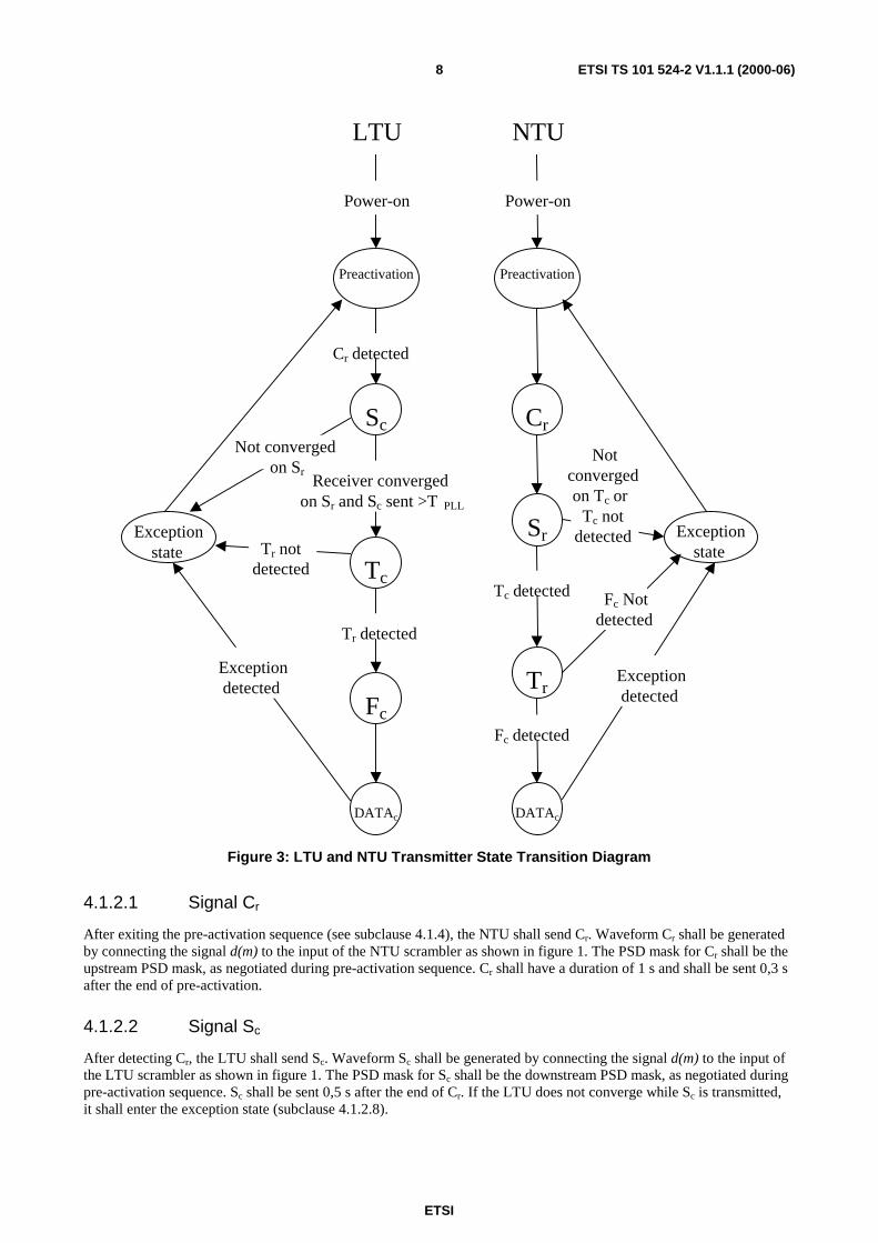
Table 4: Timeout values
Parameter Name ValueMaximum time from start of Cr to Datar Tact 15 sTime from start of Datac or Datar to valid SDSL payload data TPayloadValid 1 sMinimum silence time from exception condition to start of train TSilence 2 sTime from start of Sc to NTU PLL lock TPLL 5 s
4.2 PMD pre-activation sequenceThis subclause describes waveforms at the loop interface and associated procedures during pre-activation mode. Thedirect specification of the performance of individual receiver elements is avoided when possible. Instead, the transmittercharacteristics are specified on an individual basis and the receiver performance is specified on a general basis as theaggregate performance of all receiver elements. Exceptions are made for cases where the performance of an individualreceiver element is crucial to interoperability.
4.2.1 PMD pre-activation reference model
The reference model of the pre-activation mode of an LTU or NTU transmitter is shown in figure 4.
SpectralShaper
MapperScramblerd(m) s(m) y(m)
z(t)
logicalones
output atloop
interface
PACCHandshake
Probe
Figure 4: Pre-activation reference model
The time index m represents the symbol time, and t represents analogue time. Since the probe signal uses 2-PAMmodulation, the bit time is equivalent to the symbol time. The output of the scrambler is s(m). The output of the mapperis y(m) and the output of the spectral shaper at the loop interface is z(t). d(m) is an initialization signal that shall belogical ones for all m. The probe modulation format shall be uncoded 2-PAM, with the symbol rate, spectral shape,duration, and power back-off selected by PACC. Probe results shall be exchanged by PACC.
4.2.2 PMD pre-activation sequence description
A typical timing diagram for the pre-activation sequence is given in figure 5. Each signal in the pre-activation sequenceshall satisfy the tolerance values listed in table 5.
LTU
NTU
tprd tps
tph
tps
tpstpcd
Pr1 Pr2 Pr3
Pc1 Pc2
tprd tprd
tpcd
tprcthp
PACC PACC
Figure 5: Typical timing diagram for pre-activation sequence

ETSI
ETSI TS 101 524-2 V1.1.1 (2000-06)13
Table 5: Timing for pre-activation signals
Time Parameter Nominal value Tolerancethp Time from end of handshake to start of
remote probe0,2 s ±10 ms
tprd Duration of remote probe Selectable ≤ 3,1 stps Time separating two probe sequences 0,2 s ±10 mstprc Time separating last remote and first central
probe sequences0,2 s ±10 ms
tpcd Duration of central probe Selectable ≤ 3,1 stph Time from end of central probe to start of
handshake0,2 s ±10 ms
NOTE: Tolerances are relative to the nominal or ideal value. They are not cumulative across the pre-activationsequence.
4.2.2.1 Signal Pri
If the optional line probe is selected during the PACC session (see subclause 4.1.4), the NTU shall send the remoteprobe signal. The symbol rate for the remote probe signal shall be negotiated during the PACC session, and shallcorrespond to the symbol rate used during activation for the specified data rate. If multiple remote probe symbol ratesare negotiated during the PACC session, then multiple probe signals will be generated, starting with lowest symbol ratenegotiated and ending with the highest symbol rate negotiated. Pri is the ith probe signal (corresponding to the ith symbolrate negotiated). Waveform Pri shall be generated by connecting the signal d(m) to the input of the NTU scrambler asshown in figure 4. The PSD mask for Pri shall be the upstream PSD mask used for signal Cr at the same symbol rate,and shall be selectable between the PSDs for activating at data rates of 192 kbit/s to 2 304 kbit/s in steps of 64 kbit/s.The duration (tprd) and power back-off shall be the same for all Pri, and shall be negotiated during the PACC session.The duration shall be selectable between 50 ms and 3,1 s in steps of 50 ms, and the power back-off shall be selectablebetween 0 dB and 15 dB in steps of 1 dB. The probe signal power back-off can be selected using either the receivedPACC signal power or a priori knowledge. If no information is available, implementers are encouraged to select aprobe power back-off of at least 6 dB. The first remote probe signal shall begin thp seconds after the end of the PACCsession. There shall be a tps second silent interval between successive remote probe signals.
4.2.2.2 Signal Pci
The LTU shall send the central probe signal tprc seconds after the end of the last remote probe signal. The symbol ratefor the central probe signal shall be negotiated during the PACC session, and shall correspond to the symbol rate usedduring activation for the specified data rate. If multiple central probe symbol rates are negotiated during the PACCsession, then multiple probe signals will be generated, starting with lowest symbol rate negotiated and ending with thehighest symbol rate negotiated. Waveform Pci is the ith probe signal (corresponding to the ith symbol rate negotiated).Waveform Pci shall be generated by connecting the signal d(m) to the input of the LTU scrambler as shown in figure 4.The PSD mask for Pci shall be the downstream PSD mask used for signal Sc at the same symbol rate, and shall beselectable between the PSDs for activating at data rates of 192 kbit/s to 2 304 kbit/s in steps of 64 kbit/s. The duration(tpcd) and power back-off shall be the same for all Pci, and shall be negotiated during the PACC session. The durationshall be selectable between 50 ms and 3,1 s in steps of 50 ms, and the power back-off shall be selectable between 0 dBand 15 dB in steps of 1 dB. The probe signal power back-off can be selected using either the received PACC signalpower or a priori knowledge. If no information is available, implementers are encouraged to select a probe power back-off of at least 6 dB. There shall be a tps silent interval between successive central probe signals, and there shall be a tph
second silent interval between the last central probe signal and the start of the following PACC session.
4.2.3 Scrambler
The scrambler used in the PMD pre-activation has the same basic structure as the data mode scrambler, but can havedifferent scrambler polynomial. During PACC session the scrambler polynomial for each probe sequence is selected bythe receiver from the set of allowed scrambler polynomials listed in table 6. The transmitter shall support all thepolynomials in table 6. During PMD pre-activation the transmit scrambler shall use the scrambler polynomial selectedby the receiver during the PACC session. The scrambler shall be initialized to all zero.
ETSI
ETSI TS 101 524-2 V1.1.1 (2000-06)14
Table 6: Pre-activation scrambler polynomials
Index LTU polynomial NTU polynomial0 ( ) ( ) ( ) ( )ndnsnsns ⊕−⊕−= 235 )()23()18()( ndnsnsns ⊕−⊕−=1 )()1()( ndnsns ⊕−= )()1()( ndnsns ⊕−=2 )()5()2()( ndnsnsns ⊕−⊕−= )()5()3()( ndnsnsns ⊕−⊕−=3 )()6()1()( ndnsnsns ⊕−⊕−= )()6()5()( ndnsnsns ⊕−⊕−=4 )()7()3()( ndnsnsns ⊕−⊕−= )()7()4()( ndnsnsns ⊕−⊕−=5
)()8(
)4()3()2()(
ndns
nsnsnsns
⊕−⊕−⊕−⊕−=
)()8(
)6()5()4()(
ndns
nsnsnsns
⊕−⊕−⊕−⊕−=
4.2.4 Mapper
The output bits from the scrambler s(m), shall be mapped to the output level y(m), as described in subclause 4.1.6.
4.2.5 Spectral shaper
The same spectral shaper shall be used for data mode and activation mode as described in subclause 4.3.5.
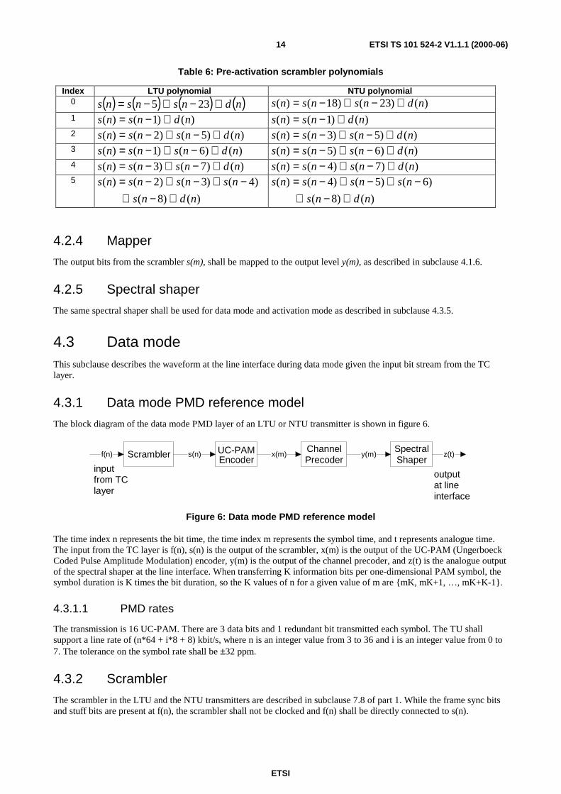
4.3 Data modeThis subclause describes the waveform at the line interface during data mode given the input bit stream from the TClayer.
4.3.1 Data mode PMD reference model
The block diagram of the data mode PMD layer of an LTU or NTU transmitter is shown in figure 6.
Scrambler UC-PAMEncoder
SpectralShaper
s(n) y(m) z(t)
inputfrom TClayer
outputat lineinterface
f(n)ChannelPrecoder
x(m)
Figure 6: Data mode PMD reference model
The time index n represents the bit time, the time index m represents the symbol time, and t represents analogue time.The input from the TC layer is f(n), s(n) is the output of the scrambler, x(m) is the output of the UC-PAM (UngerboeckCoded Pulse Amplitude Modulation) encoder, y(m) is the output of the channel precoder, and z(t) is the analogue outputof the spectral shaper at the line interface. When transferring K information bits per one-dimensional PAM symbol, thesymbol duration is K times the bit duration, so the K values of n for a given value of m are mK, mK+1, …, mK+K-1.
4.3.1.1 PMD rates
The transmission is 16 UC-PAM. There are 3 data bits and 1 redundant bit transmitted each symbol. The TU shallsupport a line rate of (n*64 + i*8 + 8) kbit/s, where n is an integer value from 3 to 36 and i is an integer value from 0 to7. The tolerance on the symbol rate shall be ±32 ppm.
4.3.2 Scrambler
The scrambler in the LTU and the NTU transmitters are described in subclause 7.8 of part 1. While the frame sync bitsand stuff bits are present at f(n), the scrambler shall not be clocked and f(n) shall be directly connected to s(n).

ETSI
ETSI TS 101 524-2 V1.1.1 (2000-06)15
4.3.3 UC-PAM encoder
The block diagram of the UC-PAM encoder is shown in figure 7. The serial bit stream from the scrambler s(n) shall beconverted to a K-bit parallel word at the mth symbol time, then processed by the convolutional encoder. The resultingK+1-bit word shall be mapped to one of 2K+1 pre-determined levels forming x(m).
ConvolutionalEncoder
Serial toParallel
Y1(m)
Y2(m)
Y0(m)
YK(m)s(mK+K-1)=XK(m)
s(mK+0)=X1(m)
s(mK+1)=X2(m) x(m)Mappers(n)
Figure 7: Block diagram of the UC-PAM encoder
4.3.3.1 Serial-to-parallel converter
The serial bit stream from the scrambler, s(n), shall be converted to a K-bit parallel wordX1(m)=s(mK), X2(m)=s(mK+1), …, XK(m)=s(mK+K-1) at the mth symbol time, where X1(m) is the first in time.
4.3.3.2 Convolutional encoder
Figure 8 shows the feedforward non-systematic convolutional encoder, where Ts is a delay of one symbol time, '⊕ ' isbinary exclusive-OR, and '⊗ ' is binary AND. X1(m) shall be applied to the convolutional encoder, Y1(m) and Y0(m)shall be computed, then X1(m) shall be shifted into the shift register.
a1a0
TsTsTs
a2
...
...
...a19 a20
b1
Y0(m)
Y1(m)
X1(m-20)X1(m-19)X1(m-1)X1(m)
b0 b2 b19 b20
Figure 8: Block diagram of the convolutional encoder

ETSI
ETSI TS 101 524-2 V1.1.1 (2000-06)16
The binary coefficients ai and bi shall be passed to the encoder from the receiver during the activation phase specified insubclause 4.1. A numerical representation of these coefficients is A and B, where:
A = a20•220+a19•219+a18•218+...+a0•20
and
B = b20•220+b19•219+b18•218+...+b0•20
The specific choice of Ungerboeck code is vendor specific. The Ungerboeck code shall be chosen such that the systemperformance requirements are satisfied.
4.3.3.3 Mapper
For K=3, the bits Y3(m), Y2(m), Y1(m), and Y0(m) shall be mapped to a level x(m) as specified in table 7.
Table 7: Data mode bit-to-level mapping
Trellis encoder output,Y3(m) Y2(m) Y1(m) Y0(m)
Level x(m)(note)
0000 -15/160001 -13/160010 -11/160011 -9/160100 -7/160101 -5/160110 -3/160111 -1/161100 1/161101 3/161110 5/161111 7/161000 9/161001 11/161010 13/161011 15/16
NOTE: The values are fractions of the value 1 asdefined in subclause 4.3.4.
4.3.4 Channel precoder
The block diagram of channel precoder is shown in figure 9, where Ts is a delay of one symbol time.

ETSI
ETSI TS 101 524-2 V1.1.1 (2000-06)17
-
+Modulo
Precoder filter
u(m)
v(m)
y(m)x(m)
XX X X
…Ts Ts Ts Ts
C 1C 2C N-1C N
y(m-N) y(m-2) y(m-1)
Figure 9: Block diagram of the channel precoder
The coefficients Ck of the precoder filter shall be transferred to the channel precoder as described in subclause 4.1.3.2.The output of the precoder filter v(m) shall be computed as follows:
v(m) C y(m k)kk 1
N
= −=
The function of the modulo block shall be to determine y(m) as follows: for each value of u(m), find an integer d(m)such that:
-1 ≤ u(m)+2d(m) < 1
and then:
y(m) = u(m)+2d(m)
4.3.5 Spectral shaper
The spectral shaper for the LTU and the NTU transmitters shall operate on the output of the respective precoders (datamode) or mappers (activation and pre-activation mode). The analogue output z(t) of the spectral shaper is coupled to theloop, and shall have a power spectral density which is limited by masks and have a limited total power. Power andpower spectral density is measured into a load impedance of 135 Ω. The power spectral density for all modes, includingpre-activation probing signals, shall be measured using a 3 kHz wide sliding window. The test procedure for transmitpower compliance is specified in TBD.
4.4 PSD masksFor all data rates, the measured transmit PSD of each LTU OR NTU shall not exceed the PSD masks specified in thissubclause (PSDMASKSDSL(f)), and the measured total power measured into a load impedance of 135 Ω shall fall withinthe range specified in this subclause (PSDSL ± 0,5 dB). The symmetric PSD masks shall be mandatory, and theasymmetric PSD masks shall be optional. Table 8 lists the supported PSDs and the associated constellation sizes.

ETSI
ETSI TS 101 524-2 V1.1.1 (2000-06)18
Table 8: PSD and constellation size
Symmetric PSDs Asymmetric PSDsDS US DS US DS USCoded 16-PAM Coded 16-PAM Coded 16-PAM Coded 16-PAM Coded 8-PAM Coded 16-PAM
Mandatory Optional For further study
4.4.1 Symmetric PSD masks
For all values of framed data rate available in the LTU OR NTU, the following set of PSD masks (PSDMASKSDSL(f))shall be selectable:
<≤××
<×
+
×
×××=
−−
×
MHz5,1ff,f100,5683
ff,10
f
f1
1
f
fπ
f
fπsin
f
1
135
KPBO(f)PSDMASK
int1,54
int10
dB(f)MaskOffset
Order2
3dB
2
sym
2
sym
sym
SDSLSDSL
see table 10, 1,5 MHz ≤ f ≤ 11,040 MHz
The inband PSD for 0 < f < 1,5 MHz shall be measured with a 10 kHz resolution bandwidth.
Where MaskOffsetdB(f) is defined as:
≥
<−
×+=3dB
3dB3dB
3dB
ff,1
ff,f
ff0,41
dB(f)MaskOffset
fint is the frequency where the two equations governing PSDMASKSDSL(f) intersect. PBO is the linear power back-offscale value. KSDSL, Order, N, fsym, f3dB, and PSDSL are defined in table 9. PSDSL is the range of power in the transmit PSDwith 0 dB power back-off. R is the payload data rate.
Table 9: Symmetric PSD parameters
Payload Data Rate, R KSDSL Order fsym f3dB PSDSL
R < 2 048 kbit/s 7,86 6 (R+8 kbit/s)/3 1,0xfsym/2 P1(R) ≤ PSDSL ≤ 13,5 dBmR ≥ 2 048 kbit/s 9,90 6 (R+8 kbit/s)/3 1,0xfsym/2 14,5 dBm
P1(R) -with R given in Hz- is defined as follows:
P1(R) = 0,3486 log2 (R + 8 000) + 6,06
For 0 dB power back-off, the measured transmit power measured into a load impedance of 135 Ω shall fall within therange PSDSL ± 0,5 dB. For power back-off values other than 0 dB, the measured transmit power measured into a loadimpedance of 135 Ω shall fall within the range PSDSL ± 0,5 dB minus the power back-off value in dB. The measuredtransmit PSD measured into a load impedance of 135 Ω shall remain below PSDMASKSDSL(f).
Table 10: Out of band limitation
Frequency band PSD constraint (note)1,5 MHz ≤ f ≤ 11,04 MHz -90 dBm/Hz peak with maximum power in a [f, f+1 MHz] window of –50 dBmNOTE: This value is under study and may change to reflect a common value for all DSL systems.

ETSI
ETSI TS 101 524-2 V1.1.1 (2000-06)19
Figure 10 shows the PSD masks with 0 dB power back-off for framed data rates of 256 kbit/s, 512 kbit/s, 768 kbit/s,1 536 kbit/s, 2 048 kbit/s and 2 304 kbit/s plus 8 kbit/s.
0 0,2 0,4 0,6 0,8 1
-110
-100
-90
-80
-70
-60
-50
-40
-30
Frequency (MHz)
PS
D(d
Bm
/Hz)
Figure 10: Symmetric PSD masks for 0 dB power back-off
The equation for the nominal PSD measured at the terminals is:
<≤
<+
×
+
×
×××= ×
MHz5,1ff,)FloorPSD(f
ff,ff
f
f
f1
1
f
fπ
f
fπsin
f
1
135
KPBO(f)NominalPSD
int
int2c
2
2
Order2
3dB
2
sym
2
sym
sym
SDSL
see table 10, 1,5 MHz ≤ f ≤ 11,040 MHz
The inband PSD for 0 < f < 1,5 MHz shall be measured with a 10 kHz resolution bandwidth.
Where fc is the transformer cutoff frequency, assumed to be 5 kHz. Figure 11 shows the nominal transmit PSDs with13,5 dBm power for framed data rates of 256 kbit/s, 512 kbit/s, 768 kbit/s, 1 536 kbit/s, 2 048 kbit/s and 2 304 kbit/splus 8 kbit/s.
NOTE: The nominal PSD is given for information only.

ETSI
ETSI TS 101 524-2 V1.1.1 (2000-06)20
0 0,2 0,4 0,6 0,8 1
-110
-100
-90
-80
-70
-60
-50
-40
-30
Frequency (MHz)
PS
D(d
Bm
/Hz)
Figure 11: Nominal symmetric PSDs for 0 dB power back-off
4.4.2 Asymmetric 2 048 kbit/s and 2 304 kbit/s PSD masks
The asymmetric PSD mask set specified in this subclause shall optionally be supported for the 2 048 kbit/s and the2 304 kbit/s payload data rate (note). Power and power spectral density is measured into a load impedance of 135 Ω.
NOTE: Other optional asymmetric PSD masks are for further study.
For the 2 048 kbit/s and the 2 304 kbit/s payload data rates available in the LTU OR NTU, the following set of PSDmasks (PSDMASKSDSL(f)) shall be selectable:
<≤××
<×
+
×
×××=
−−
×
MHz5,1ff,f100,5683
ff,10
f
f1
1
f
fπ
f
fπsin
f
1
135
KPBO
(f)PSDMASK
int1,54
int10
dB(f)MaskOffset
Order2
3dB
2
x
2
x
x
SDSL
SDSL
see table 10, 1,5 MHz ≤ f ≤ 11,040 MHz
The inband PSD for 0 < f < 1,5 MHz shall be measured with a 10 kHz resolution bandwidth.
Where MaskOffsetdB(f) is defined as:
≥
<−
×+=3dB
3dB3dB
3dB
ff,1
ff,f
ff0,41
dB(f)MaskOffset

ETSI
ETSI TS 101 524-2 V1.1.1 (2000-06)21
fint is the frequency where the two equations governing PSDMASKSDSL(f) intersect. PBO is the linear power back-offscale value. KSDSL, Order, fx, f3dB and PSDSL are defined in table 11. PSDSL is the range of power in the transmit PSD with0 dB power back-off. R is the payload data rate.
Table 11: Asymmetric PSD parameters
Payload data rate Transmitter KSDSL Order fx f3dB PSDSL
2 048 kbit/s LTU16,86
7 1 370 667 Hz 548 267 Hz 16,25 dBm
2 048 kbit/s NTU 15,66 7 685 333 Hz 342 667 Hz 16,50 dBm2 304 kbit/s LTU
12,487 1 541 333 Hz 578 000 Hz 14,75 dBm
2 304 kbit/s NTU 11,74 7 770 667 Hz 385 333 Hz 15,25 dBm
For 0 dB power back-off, the measured transmit power measured into a load impedance of 135 Ω shall fall within therange PSDSL ± 0,5 dB. For power back-off values other than 0 dB, the measured transmit power measured into a loadimpedance of 135 Ω shall fall within the range PSDSL ± 0,5 dB minus the power back-off value in dB. The measuredtransmit PSD measured into a load impedance of 135 Ω shall remain below PSDMASKSDSL(f).
Figure 2 shows the asymmetric PSD masks with 0 dB power back-off for payload data rates of 2 048 kbit/s and2 304 kbit/s.
0 0,2 0,4 0,6 0,8 1
-110
-100
-90
-80
-70
-60
-50
-40
-30
Frequency (MHz)
PS
D(d
Bm
/Hz)
Figure 12: Asymmetric PSD masks for 0 dB power back-off

ETSI
ETSI TS 101 524-2 V1.1.1 (2000-06)22
The equation for the nominal PSD measured at the terminals is:
<≤
<+
×
+
×
×××= ×
1,5MHzff,)FloorPSD(f
ff,ff
f
f
f1
1
f
fπ
f
fπsin
f
1
135
KPBO(f)NominalPSD
int
int2c
2
2
Order2
3dB
2
x
2
x
x
SDSL
see table 10, 1,5 MHz ≤ f ≤ 11,040 MHz
The inband PSD for 0 < f < 1,5 MHz shall be measured with a 10 kHz resolution bandwidth.
Where fc is the transformer cutoff frequency, assumed to be 5 kHz. Figure 13 shows the nominal transmit PSDs with0 dB power back-off for payload data rates of 2 048 kbit/s and 2 304 kbit/s.
NOTE: The nominal PSD is given for information only.
0 0,2 0,4 0,6 0,8 1
-110
-100
-90
-80
-70
-60
-50
-40
-30
Frequency (MHz)
PS
D(d
Bm
/Hz)
Figure 13: Nominal asymmetric PSDs for 0 dB power back-off

ETSI
ETSI TS 101 524-2 V1.1.1 (2000-06)23
History
Document history
V1.1.1 June 2000 Publication